WO2020044817A1 - 光源装置、検出方法、センシングモジュール - Google Patents
光源装置、検出方法、センシングモジュール Download PDFInfo
- Publication number
- WO2020044817A1 WO2020044817A1 PCT/JP2019/027701 JP2019027701W WO2020044817A1 WO 2020044817 A1 WO2020044817 A1 WO 2020044817A1 JP 2019027701 W JP2019027701 W JP 2019027701W WO 2020044817 A1 WO2020044817 A1 WO 2020044817A1
- Authority
- WO
- WIPO (PCT)
- Prior art keywords
- light emitting
- light
- voltage
- unit
- source device
- Prior art date
- Legal status (The legal status is an assumption and is not a legal conclusion. Google has not performed a legal analysis and makes no representation as to the accuracy of the status listed.)
- Ceased
Links
Images








Classifications
-
- G—PHYSICS
- G01—MEASURING; TESTING
- G01B—MEASURING LENGTH, THICKNESS OR SIMILAR LINEAR DIMENSIONS; MEASURING ANGLES; MEASURING AREAS; MEASURING IRREGULARITIES OF SURFACES OR CONTOURS
- G01B11/00—Measuring arrangements characterised by the use of optical techniques
- G01B11/24—Measuring arrangements characterised by the use of optical techniques for measuring contours or curvatures
- G01B11/25—Measuring arrangements characterised by the use of optical techniques for measuring contours or curvatures by projecting a pattern, e.g. one or more lines, moiré fringes on the object
- G01B11/2513—Measuring arrangements characterised by the use of optical techniques for measuring contours or curvatures by projecting a pattern, e.g. one or more lines, moiré fringes on the object with several lines being projected in more than one direction, e.g. grids, patterns
-
- G—PHYSICS
- G01—MEASURING; TESTING
- G01S—RADIO DIRECTION-FINDING; RADIO NAVIGATION; DETERMINING DISTANCE OR VELOCITY BY USE OF RADIO WAVES; LOCATING OR PRESENCE-DETECTING BY USE OF THE REFLECTION OR RERADIATION OF RADIO WAVES; ANALOGOUS ARRANGEMENTS USING OTHER WAVES
- G01S17/00—Systems using the reflection or reradiation of electromagnetic waves other than radio waves, e.g. lidar systems
- G01S17/02—Systems using the reflection of electromagnetic waves other than radio waves
- G01S17/06—Systems determining position data of a target
- G01S17/08—Systems determining position data of a target for measuring distance only
- G01S17/10—Systems determining position data of a target for measuring distance only using transmission of interrupted, pulse-modulated waves
-
- G—PHYSICS
- G01—MEASURING; TESTING
- G01S—RADIO DIRECTION-FINDING; RADIO NAVIGATION; DETERMINING DISTANCE OR VELOCITY BY USE OF RADIO WAVES; LOCATING OR PRESENCE-DETECTING BY USE OF THE REFLECTION OR RERADIATION OF RADIO WAVES; ANALOGOUS ARRANGEMENTS USING OTHER WAVES
- G01S17/00—Systems using the reflection or reradiation of electromagnetic waves other than radio waves, e.g. lidar systems
- G01S17/88—Lidar systems specially adapted for specific applications
- G01S17/89—Lidar systems specially adapted for specific applications for mapping or imaging
-
- G—PHYSICS
- G01—MEASURING; TESTING
- G01S—RADIO DIRECTION-FINDING; RADIO NAVIGATION; DETERMINING DISTANCE OR VELOCITY BY USE OF RADIO WAVES; LOCATING OR PRESENCE-DETECTING BY USE OF THE REFLECTION OR RERADIATION OF RADIO WAVES; ANALOGOUS ARRANGEMENTS USING OTHER WAVES
- G01S7/00—Details of systems according to groups G01S13/00, G01S15/00, G01S17/00
- G01S7/48—Details of systems according to groups G01S13/00, G01S15/00, G01S17/00 of systems according to group G01S17/00
- G01S7/483—Details of pulse systems
- G01S7/484—Transmitters
-
- G—PHYSICS
- G01—MEASURING; TESTING
- G01S—RADIO DIRECTION-FINDING; RADIO NAVIGATION; DETERMINING DISTANCE OR VELOCITY BY USE OF RADIO WAVES; LOCATING OR PRESENCE-DETECTING BY USE OF THE REFLECTION OR RERADIATION OF RADIO WAVES; ANALOGOUS ARRANGEMENTS USING OTHER WAVES
- G01S7/00—Details of systems according to groups G01S13/00, G01S15/00, G01S17/00
- G01S7/48—Details of systems according to groups G01S13/00, G01S15/00, G01S17/00 of systems according to group G01S17/00
- G01S7/497—Means for monitoring or calibrating
-
- H—ELECTRICITY
- H01—ELECTRIC ELEMENTS
- H01S—DEVICES USING THE PROCESS OF LIGHT AMPLIFICATION BY STIMULATED EMISSION OF RADIATION [LASER] TO AMPLIFY OR GENERATE LIGHT; DEVICES USING STIMULATED EMISSION OF ELECTROMAGNETIC RADIATION IN WAVE RANGES OTHER THAN OPTICAL
- H01S5/00—Semiconductor lasers
- H01S5/0014—Measuring characteristics or properties thereof
- H01S5/0028—Laser diodes used as detectors
-
- H—ELECTRICITY
- H01—ELECTRIC ELEMENTS
- H01S—DEVICES USING THE PROCESS OF LIGHT AMPLIFICATION BY STIMULATED EMISSION OF RADIATION [LASER] TO AMPLIFY OR GENERATE LIGHT; DEVICES USING STIMULATED EMISSION OF ELECTROMAGNETIC RADIATION IN WAVE RANGES OTHER THAN OPTICAL
- H01S5/00—Semiconductor lasers
- H01S5/04—Processes or apparatus for excitation, e.g. pumping, e.g. by electron beams
- H01S5/042—Electrical excitation ; Circuits therefor
-
- G—PHYSICS
- G01—MEASURING; TESTING
- G01S—RADIO DIRECTION-FINDING; RADIO NAVIGATION; DETERMINING DISTANCE OR VELOCITY BY USE OF RADIO WAVES; LOCATING OR PRESENCE-DETECTING BY USE OF THE REFLECTION OR RERADIATION OF RADIO WAVES; ANALOGOUS ARRANGEMENTS USING OTHER WAVES
- G01S7/00—Details of systems according to groups G01S13/00, G01S15/00, G01S17/00
- G01S7/48—Details of systems according to groups G01S13/00, G01S15/00, G01S17/00 of systems according to group G01S17/00
- G01S7/481—Constructional features, e.g. arrangements of optical elements
- G01S7/4814—Constructional features, e.g. arrangements of optical elements of transmitters alone
- G01S7/4815—Constructional features, e.g. arrangements of optical elements of transmitters alone using multiple transmitters
-
- H—ELECTRICITY
- H01—ELECTRIC ELEMENTS
- H01S—DEVICES USING THE PROCESS OF LIGHT AMPLIFICATION BY STIMULATED EMISSION OF RADIATION [LASER] TO AMPLIFY OR GENERATE LIGHT; DEVICES USING STIMULATED EMISSION OF ELECTROMAGNETIC RADIATION IN WAVE RANGES OTHER THAN OPTICAL
- H01S5/00—Semiconductor lasers
- H01S5/04—Processes or apparatus for excitation, e.g. pumping, e.g. by electron beams
- H01S5/042—Electrical excitation ; Circuits therefor
- H01S5/0428—Electrical excitation ; Circuits therefor for applying pulses to the laser
-
- H—ELECTRICITY
- H01—ELECTRIC ELEMENTS
- H01S—DEVICES USING THE PROCESS OF LIGHT AMPLIFICATION BY STIMULATED EMISSION OF RADIATION [LASER] TO AMPLIFY OR GENERATE LIGHT; DEVICES USING STIMULATED EMISSION OF ELECTROMAGNETIC RADIATION IN WAVE RANGES OTHER THAN OPTICAL
- H01S5/00—Semiconductor lasers
- H01S5/40—Arrangement of two or more semiconductor lasers, not provided for in groups H01S5/02 - H01S5/30
- H01S5/42—Arrays of surface emitting lasers
- H01S5/423—Arrays of surface emitting lasers having a vertical cavity
Definitions
- the present technology is directed to a light source device including a light emitting unit in which a plurality of light emitting elements by a vertical cavity surface emitting laser are arranged, a detection method for detecting a voltage of the light emitting element, and a light emitted from the light emitting unit and reflected by a subject.
- the present invention relates to a sensing module including an image sensor that receives light and captures an image.
- a light emitting element as a VCSEL Vertical Cavity Surface Emitting LASER
- a light emitting element as a VCSEL is configured such that a resonator is formed in a direction perpendicular to a semiconductor substrate surface and emits a laser beam in a vertical direction.
- an STL Structured Light: structured light
- Method or a time-of-flight (ToF) method is widely used as a light source when measuring the distance of a subject.
- a light source device in which a plurality of light emitting elements as a VCSEL are two-dimensionally arranged is used. Specifically, the object is irradiated with light obtained by emitting the light from the plurality of light emitting elements, and distance measurement of the object is performed based on an image obtained by receiving reflected light from the object.
- the light emitting element in order to cause the light emitting element to emit light appropriately, it is effective to control the power supply voltage or stop the circuit by detecting the voltage generated in the light emitting element. In order to enhance safety, it is effective to control the power supply voltage by detecting a voltage abnormality of the light emitting element.
- the present technology has been made in view of the above circumstances, and it is possible to separately detect a voltage for each light emitting element in a light source device including a light emitting unit in which a plurality of light emitting elements by a vertical cavity surface emitting laser are arranged. It is an object of the present invention to reduce the size of the device while reducing the size of the device.
- a light source device includes a light emitting unit in which a plurality of light emitting elements by a vertical cavity surface emitting laser are arranged, and a detecting unit that individually detects voltages at anodes or cathodes of the plurality of light emitting elements in the light emitting unit by time division. Is provided.
- the detection unit includes a counter that switches the light-emitting element to be detected according to a clock and counts in synchronization with the clock.
- the detection unit includes a voltage detection line for each of the light-emitting elements and a voltage follower inserted for each of the detection lines and configured to be capable of ON / OFF control. Is desirable.
- the light source device further includes a drive circuit that supplies a drive current to the plurality of light emitting elements by a current mirror circuit.
- the current mirror circuit is connected to an anode side of the light emitting element, and the detection unit detects a voltage at an anode of the light emitting element.
- the current mirror circuit is connected to a cathode side of the light emitting element, and the detection unit detects a voltage at a cathode of the light emitting element.
- the light source device further includes a determination unit that determines an abnormality of the light emitting element based on the voltage individually detected by the detection unit.
- the determination unit determines whether or not the voltage value is within a predetermined range as determination of whether or not the light emitting element is abnormal.
- a power supply circuit that generates a power supply voltage commonly used for driving a plurality of the light emitting elements, and a control that controls the power supply circuit based on the voltage detected by the detection unit. It is desirable to have a part.
- control unit controls the power supply circuit so as to increase the power supply voltage in response to the detection unit detecting the voltage equal to or higher than a predetermined threshold.
- the height of the common power supply voltage is adjusted in accordance with the voltage of the light emitting element having a high detection voltage. Is made possible.
- the light source device further includes a drive circuit including a switch provided for each of the light emitting elements and configured to individually drive the light emitting elements in the light emitting unit.
- a detection method is a detection method in which voltages at the anodes or cathodes of a plurality of light emitting elements in a light emitting unit in which a plurality of light emitting elements by a vertical cavity surface emitting laser are arranged are time-divided.
- a sensing module includes the light source device according to the present technology described above, and an image sensor that receives light reflected from a subject and emitted from a light emitting unit included in the light source device and captures an image. .
- a light source device including a light emitting unit in which a plurality of light emitting elements using a vertical cavity surface emitting laser are arranged, it is possible to detect and separate a voltage for each light emitting element and reduce the size of the device. be able to.
- the effects described here are not necessarily limited, and may be any of the effects described in the present disclosure.
- FIG. 1 is a diagram illustrating a configuration example of a distance measuring device as an embodiment of a light source device according to the present technology.
- FIG. 3 is an explanatory diagram of a distance measurement method based on an STL (Structured @ Light) method. It is a figure showing an example of circuit composition of a light source device as an embodiment.
- FIG. 9 is a diagram illustrating a modification of the drive circuit included in the light source device according to the embodiment.
- FIG. 9 is a diagram illustrating a circuit configuration as a modification of the light source device according to the embodiment.
- FIG. 3 is a diagram illustrating a substrate configuration example of a light source device as an embodiment.
- FIG. 9 is a diagram illustrating another example of the substrate configuration of the light source device according to the embodiment.
- FIG. 9 is a diagram illustrating still another example of the substrate configuration of the light source device according to the embodiment. It is a figure showing an example of arrangement of a temperature sensor with which a light source device as an embodiment is provided. It is a figure showing an example of structure of a light emitting part with which a light source device as an embodiment is provided.
- FIG. 9 is a diagram illustrating another example of the structure of the light emitting unit included in the light source device according to the embodiment.
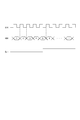
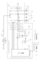
- FIG. 2 is an explanatory diagram illustrating a configuration example for implementing voltage detection as an embodiment.
- FIG. 3 is a diagram illustrating a relationship between a clock used for time-division detection, a voltage value (HDR) detected by time-division, and an abnormality detection signal according to the embodiment.
- HDR voltage value
- FIG. 5 is a flowchart illustrating a specific procedure of processing to be executed in implementing abnormality determination and power control according to the embodiment.
- FIG. 4 is a diagram illustrating an example of an arrangement of components of a driving unit that drives a light emitting unit on a chip. It is explanatory drawing about the modification which omitted the counter. It is explanatory drawing about the modification which uses the voltage follower with an enable function.
- FIG. 1 shows a configuration example of a distance measuring device 1 as one embodiment of a light source device according to the present technology.
- the distance measuring device 1 includes a light emitting unit 2, a driving unit 3, a power supply circuit 4, a light emitting side optical system 5, an imaging side optical system 6, an image sensor 7, an image processing unit 8, a control unit 9, and a temperature detection.
- a section 10 is provided.
- the light emitting unit 2 emits light from a plurality of light sources.
- the light emitting section 2 of the present embodiment has light emitting elements 2a formed by VCSELs (Vertical Cavity Surface Emitting LASER) as light sources, and the light emitting elements 2a are arranged in a matrix or the like. Are arranged in a predetermined manner.
- VCSELs Vertical Cavity Surface Emitting LASER
- the driving unit 3 includes an electric circuit for driving the light emitting unit 2.
- the power supply circuit 4 generates a power supply voltage (an output voltage Vo described later) of the drive unit 3 based on an input voltage (an input voltage Vin described later) from, for example, a battery (not shown) provided in the distance measuring device 1.
- the driving unit 3 drives the light emitting unit 2 based on the power supply voltage.
- the light emitted from the light emitting unit 2 is irradiated to the subject S as a distance measurement target via the light emitting side optical system 5. Then, the reflected light of the light emitted from the subject S enters the imaging surface of the image sensor 7 via the imaging-side optical system 6.
- the image sensor 7 is, for example, an image sensor such as a CCD (Charge Coupled Device) sensor or a CMOS (Complementary Metal Oxide Semiconductor) sensor.
- the light is received, converted into an electric signal and output.
- the image sensor 7 performs, for example, CDS (Correlated Double Sampling) processing, AGC (Automatic Gain Control) processing, and the like on an electric signal obtained by photoelectrically converting the received light, and further performs A / D (Analog / Digital) conversion. Perform processing.
- an image signal as digital data is output to the image processing unit 8 at the subsequent stage.
- the image sensor 7 of the present example outputs the frame synchronization signal Fs to the drive unit 3.
- the driving unit 3 can cause the light emitting element 2a of the light emitting unit 2 to emit light at a timing corresponding to the frame period of the image sensor 7.
- the image processing unit 8 is configured as an image processor by, for example, a DSP (Digital Signal Processor) or the like.
- the image processing unit 8 performs various types of image signal processing on a digital signal (image signal) input from the image sensor 7.
- the control unit 9 includes, for example, a microcomputer having a CPU (Central Processing Unit), a ROM (Read Only Memory), a RAM (Random Access Memory), or an information processing device such as a DSP.
- the control of the drive unit 3 for controlling the operation and the control relating to the imaging operation by the image sensor 7 are performed.
- the control unit 9 has a function as a distance measuring unit 9a.
- the distance measuring unit 9a measures a distance to the subject S based on an image signal input through the image processing unit 8 (that is, an image signal obtained by receiving light reflected from the subject S).
- the distance measuring unit 9a of the present example measures the distance of each part of the subject S in order to enable the three-dimensional shape of the subject S to be specified. Will be described later.
- the temperature detector 10 detects the temperature of the light emitting unit 2.
- the temperature detection unit 10 can adopt a configuration for performing temperature detection using, for example, a diode.
- the information on the temperature detected by the temperature detection unit 10 is supplied to the driving unit 3, whereby the driving unit 3 can drive the light emitting unit 2 based on the information on the temperature.
- a distance measuring method in the distance measuring apparatus for example, a distance measuring method using an STL (Structured Light) method or a ToF (Time of Flight) method can be adopted.
- the STL method is a method of measuring a distance based on an image obtained by imaging a subject S irradiated with light having a predetermined light and dark pattern such as a dot pattern or a grid pattern.
- FIG. 2 is an explanatory diagram of the STL method.
- FIG. 2B is a diagram illustrating the principle of ranging in the STL method.
- the wall W and the box BX disposed in front of the wall W are the subject S, and the subject S is irradiated with the pattern light Lp.
- BLn means the light of a certain block BL in the pattern light Lp
- dn means the dot pattern of the block BLn displayed on the image captured by the image sensor 7.
- the dot pattern of the block BLn is displayed at the position of “dn ′” in the captured image. That is, the position where the pattern of the block BLn is projected in the captured image is different between the case where the box BX exists and the case where the box BX does not exist, and specifically, the pattern is distorted.
- the STL method is a method of obtaining the shape and depth of the subject S by utilizing the fact that the irradiated pattern is distorted by the shape of the subject S. Specifically, it is a method of obtaining the shape and depth of the subject S from the pattern distortion.
- the distance measuring unit 9a controls the driving unit 3 so that the light emitting unit 2 emits the pattern light, and detects a pattern distortion of an image signal obtained via the image processing unit 8. , The distance is calculated based on how the pattern is distorted.
- the ToF method measures the distance to the object by detecting the flight time (time difference) of the light from the light emitting unit 2 until the light is reflected by the object and reaches the image sensor 7. It is a method to do.
- a so-called direct ToF method is adopted as the ToF method, a single photon avalanche diode (SPAD) is used as the image sensor 7, and the light emitting unit 2 is pulse-driven.
- the distance measuring unit 9a calculates a time difference from light emission to light reception of light emitted from the light emitting unit 2 and received by the image sensor 7 based on the image signal input via the image processing unit 8, The distance of each part of the subject S is calculated based on the time difference and the speed of light.
- a so-called indirect ToF method phase difference method
- an IR image sensor is used as the image sensor 7.
- FIG. 3 illustrates a circuit configuration example of a light source device 100 configured including the light emitting unit 2, the driving unit 3, and the power supply circuit 4 illustrated in FIG.
- FIG. 3 shows the image sensor 7 and the control unit 9 shown in FIG. 1 together with an example of the circuit configuration of the light source device 100.
- the light emitting unit 2, the driving unit 3, and the power supply circuit 4 are formed on a common substrate (substrate B described later).
- a structural unit including at least the light emitting unit 2 and formed on a common substrate with the light emitting unit 2 is called a light source device 100.
- the light source device 100 includes a light emitting unit 2, a driving unit 3, a power supply circuit 4, and a temperature detecting unit 10.
- the light emitting section 2 includes a plurality of light emitting elements 2a as VCSELs as described above.
- the number of light emitting elements 2 a is “4” for convenience of illustration, but the number of light emitting elements 2 a in the light emitting unit 2 is not limited to this, and may be at least two.
- the power supply circuit 4 includes a DC / DC converter 40, and generates an output voltage Vo based on a DC voltage based on an input voltage Vin based on a DC voltage.
- This output voltage Vo is used as a power supply voltage for the drive unit 3 to drive the light emitting unit 2.
- the DC / DC converter 40 is configured to be able to adjust the height (current value) of the output voltage Vo.
- the drive unit 3 includes a drive circuit 30 and a drive control unit 31.
- the drive circuit 30 has a drive element Q1 and a switch SW for each light emitting element 2a, and has a current control element Q2 and a constant current source 30a.
- An FET field-effect transistor
- MOS metal-oxide-semiconductor
- Each driving element Q1 is connected in parallel with the output line of the DC / DC converter 40, that is, the supply line of the output voltage Vo, and the current control element Q2 is connected in parallel with the driving element Q1.
- the source of each of the driving element Q1 and the current control element Q2 is connected to the output line of the DC / DC converter 40.
- the drain of each driving element Q1 is connected to the anode of one corresponding light emitting element 2a among the light emitting elements 2a in the light emitting section 2. As shown, the cathode of each light emitting element 2a is connected to ground (GND).
- the current control element Q2 has a drain connected to the ground via the constant current source 30a, and a gate connected to a connection point between the drain and the constant current source 30a.
- the gate of each drive element Q1 is connected to the gate of the current control element Q2 via one corresponding switch SW.
- the drive element Q1 whose switch SW is turned on is turned on, and the drive voltage Vd based on the output voltage Vo is applied to the light emitting element 2a connected to the turned on drive element Q1.
- the element 2a emits light.
- the drive current Id flows through the light emitting element 2a, but in the drive circuit 30 having the above configuration, the drive element Q1 and the current control element Q2 form a current mirror circuit, and the current value of the drive current Id is a constant current. It is controlled to a value corresponding to the current value of the source 30a.
- the drive control unit 31 controls ON / OFF of the light emitting element 2a by performing ON / OFF control of the switch SW in the drive circuit 30.
- control signal lines for the drive control unit 31 to individually control ON / OFF of each switch SW are described as control signal lines Ls.
- the drive control unit 31 is supplied with the frame synchronization signal Fs from the image sensor 7, whereby the drive control unit 31 can synchronize the ON timing and the OFF timing of the light emitting element 2 a with the frame period of the image sensor 7. Have been. Further, the drive control unit 31 is configured to be able to perform ON / OFF control of the light emitting element 2 a based on an instruction from the control unit 9.
- the drive control unit 31 can also perform ON / OFF control of the light emitting element 2a based on the temperature of the light emitting unit 2 detected by the temperature detecting unit 10. Further, the drive control unit 31 can make an instruction to the DC / DC converter 40 in the power supply circuit 4 to adjust the output voltage Vo, which will be described later.
- a detection line Ld for detecting a voltage generated in the light emitting element 2a is formed in the driving unit 3 for each light emitting element 2a.
- each detection line Ld is connected to the anode of the corresponding light emitting element 2a.
- the drive control unit 31 of the present example is provided with a configuration for individually detecting the voltage obtained on each detection line Ld, that is, the voltage of each light emitting element 2a, which will be described later.
- FIG. 3 illustrates a configuration in which the current mirror circuit including the driving element Q1 and the current control element Q2 is provided on the anode side of the light emitting element 2a.
- the driving circuit 30A illustrated in FIG. It is also possible to adopt a configuration provided on the cathode side of the light emitting element 2a.
- the anode of each light emitting element 2 a in the light emitting unit 2 is connected to the output line of the DC / DC converter 40.
- an N-channel MOSFET is used for the drive element Q1 and the current control element Q2 that constitute the current mirror circuit.
- the current control element Q2 has a drain and a gate connected to the output line of the DC / DC converter 40 via the constant current source 30a, and a source connected to the ground.
- Each drive element Q1 has a drain connected to the cathode of the corresponding light emitting element 2a and a source connected to the ground.
- the gate of each drive element Q1 is connected to the gate and drain of the current control element Q2 via a corresponding switch SW.
- the drive control unit 31 performs ON / OFF control of the switch SW, so that the light emitting element 2a can be turned ON / OFF.
- each detection line Ld is connected to the cathode of the corresponding light emitting element 2a. That is, the drive control unit 31 in this case detects the voltage at the cathode of the light emitting element 2a.
- FIG. 5 shows a configuration example of a light source device 100A as a modification.
- the light source device 100A is different from the light source device 100 in that a power supply circuit 4A is provided instead of the power supply circuit 4 and a drive unit 3A is provided instead of the drive unit 3.
- the power supply circuit 4A has a plurality of DC / DC converters 40 (two in the example of the figure).
- the input voltage Vin1 is supplied to one DC / DC converter 40, and the input voltage Vin2 is supplied to the other DC / DC converter 40.
- the drive unit 3A includes a plurality of drive circuits 30 each receiving an output voltage Vo from a different DC / DC converter 40. As shown, in each drive circuit 30, a variable current source 30b is provided instead of the constant current source 30a.
- the variable current source 30b has a variable current value.
- the light-emitting elements 2a in the light-emitting unit 2 are divided into a plurality of light-emitting element groups, each of which has a different drive circuit 30 whose ON / OFF control is performed.
- the drive control unit 31 performs ON / OFF control of the switch SW in each drive circuit 30.
- a current mirror circuit including the driving element Q1 and the current control element Q2 is connected to the anode side of the light emitting element 2a. Therefore, they are connected to the anodes of the corresponding light emitting elements 2a. That is, the drive control unit 31 in this case detects the voltage at the anode of the light emitting element 2a.
- At least the group of the DC / DC converter 40 and the drive circuit 30 is divided into a plurality of systems, so that the drive current Id of the light emitting element 2a is different for each system. be able to.
- the value of the drive current Id can be made different for each system.
- the DC / DC converter 40 is configured to perform the constant current control on the drive current Id, the target value of the constant current control is made different between the respective DC / DC converters 40, so that the drive current Id is different for each system.
- the values can be different.
- the values of the output voltage Vo and the drive current Id are different for each system according to the light emission intensity distribution and the temperature distribution in the light emitting section 2.
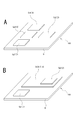
- the light source device 100 can be configured as shown in FIGS. As shown in FIG. 6A, the light source device 100 includes a chip Cp2 on which a circuit as the light emitting unit 2 is formed, a chip Cp3 on which a circuit as the drive unit 3 is formed, and a chip Cp4 on which a power supply circuit 4 is formed. May be formed on the same substrate B. In addition, the driving unit 3 and the power supply circuit 4 can be formed on the same chip Cp34. In this case, the light source device 100 forms the chip Cp2 and the chip Cp34 on the same substrate B as shown in FIG. It is also possible to adopt a configuration in which:
- a configuration in which another chip Cp is mounted on the chip Cp can also be adopted.
- the light source device 100 for example, as shown in FIG. 7A, a configuration in which the chips Cp3 and Cp4 each having the chip Cp2 mounted thereon are formed on the substrate B, or a configuration in which the chips Cp2 and Cp4 are mounted as shown in FIG.
- the chip Cp3 formed on the substrate B may be formed on the substrate B, or the chip Cp34 mounted with the chip Cp2 may be formed on the substrate B as shown in FIG.
- the light source device 100 may be configured to include the image sensor 7.
- FIG. 8A illustrates a configuration of the light source device 100 in which a chip Cp7 in which a circuit as the image sensor 7 is formed on the same substrate B together with the chips Cp2, Cp3, and Cp4.
- FIG. 8B illustrates the configuration of the light source device 100 in which the chip Cp34 having the chip Cp2 and the chip Cp7 are formed on the same substrate B.
- the light source device 100A described above can also have the same configuration as that described with reference to FIGS.
- the temperature detecting element such as a diode may be connected to the chip Cp2 on the substrate B when the chip Cp2 is formed on the substrate B as shown in FIGS. 6A, 6B and 8A. It may be formed at a nearby position (for example, a side position of the chip Cp2 on the substrate B). Further, in a configuration in which the chip Cp2 is mounted on another chip Cp as shown in FIGS. 7A to 7C and FIG. 8B, the temperature detecting element is located near the chip Cp2 in the other chip Cp (for example, at a position just below the chip Cp2). Etc.).
- the temperature detection unit 10 may be configured to include a plurality of temperature sensors 10a having a temperature detection element such as a diode.
- FIG. 9 shows an example of the arrangement of each temperature sensor 10a when the temperature detection unit 10 has a plurality of temperature sensors 10a.
- the plurality of temperature sensors 10a are not concentrated at one place, but are discretely arranged in a plane parallel to the plane on which the light emitting elements 2a are arranged.
- the temperature sensors 10a can be arranged at regular intervals in a plane parallel to the plane on which the light emitting elements 2a are arranged.
- FIG. 9 shows an example in which four temperature sensors 10a are arranged for nine light emitting elements 2a, the number of light emitting elements 2a and temperature sensors 10a is not limited to this.
- thermosensor 10a By arranging a plurality of temperature sensors 10a discretely as in the example of FIG. 9, it is possible to detect the in-plane temperature distribution of the light emitting unit 2. Further, the temperature of each area on the light emitting surface can be detected and separated, and the temperature of each light emitting element 2a can be separately detected by increasing the number of the temperature sensors 10a.
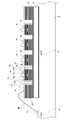
- FIG. 10 shows a structural example of a chip Cp2 formed on the substrate B as shown in FIGS. 6A, 6B and 8A
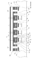
- FIG. 11 shows another chip as shown in FIGS. 7A to 7C and 8B
- 3 shows a structural example of a chip Cp2 when mounted on Cp.
- FIGS. 10 and 11 show, as an example, a structural example corresponding to the case where the drive circuit 30 (current mirror circuit) is inserted on the anode side of the light emitting element 2a (see FIG. 3).
- a portion corresponding to each light emitting element 2a is formed as a mesa M.
- the semiconductor substrate 20 is used as the substrate of the chip Cp2, and the cathode electrode Tc is formed below the semiconductor substrate 20.
- the semiconductor substrate 20 for example, a GaAs (gallium arsenide) substrate is used.
- each of the mesas M includes a first multilayer reflector layer 21, an active layer 22, a second multilayer reflector layer 25, a contact layer 26, and an anode electrode in order from the lower layer side to the upper layer side.
- Ta is formed.
- a current confinement layer 24 is formed on a part (specifically, a lower end) of the second multilayer reflector layer 25.
- a portion including the active layer 22 and sandwiched between the first multilayer reflector layer 21 and the second multilayer reflector layer 25 is a resonator 23.
- the first multilayer reflector layer 21 is formed of a compound semiconductor exhibiting N-type conductivity
- the second multilayer reflector layer 25 is formed of a compound semiconductor exhibiting P-type conductivity.
- the active layer 22 is a layer for generating a laser beam
- the current confinement layer 24 is a layer for efficiently injecting a current into the active layer 22 and providing a lens effect.
- the current confinement layer 24 is selectively oxidized in a non-oxidized state, so that a central oxidized region (or a selectively oxidized region) 24a and an unoxidized portion around the oxidized region 24a are not oxidized. And an oxidized region 24b.
- a current confinement structure is formed by the oxidized region 24a and the non-oxidized region 24b, and a current is conducted to the current confinement region as the non-oxidized region 24b.
- the contact layer 26 is provided to ensure ohmic contact with the anode electrode Ta.
- the anode electrode Ta is formed on the contact layer 26 by, for example, an annular (ring-shaped) opening at the center when the substrate B is viewed in plan.
- a portion where the anode electrode Ta is not formed on the upper portion is an opening 26a.
- the cathode electrode Tc of the chip Cp2 is connected to the ground via a ground wiring Lg formed on the wiring layer of the substrate B.
- a pad Pa represents a pad for an anode electrode formed on the substrate B.
- the pad Pa is connected to the drain of any one of the drive elements Q1 of the drive circuit 30 via the wiring Ld formed on the wiring layer of the substrate B.
- the drawing shows that, for only one light emitting element 2a, the anode electrode Ta is connected to one pad Pa via the anode wiring La and the bonding wire BW formed on the chip Cp2.
- B a pad Pa and a wiring Ld for each light emitting element 2a are formed, and an anode wiring La for each light emitting element 2a is formed on the chip Cp2.
- the anode electrode Ta of each light emitting element 2a is It is connected to the corresponding pad Pa via the corresponding anode wiring La and the bonding wire BW.
- a backside irradiation type chip Cp2 is used as the chip Cp2. That is, a chip Cp2 that emits light in the direction of the back surface of the semiconductor substrate 20 instead of emitting light in the upper layer side direction (surface direction) as in the example of FIG. 10 is used. In this case, no opening for light emission is formed in the anode electrode Ta, and no opening 26 a is formed in the contact layer 26.
- a pad for making electrical connection with the anode electrode Ta for each light emitting element 2a. Pa is formed.
- a wiring Ld is formed for each pad Pa.
- each pad Pa is connected to the drain of the corresponding one drive element Q1 in the drive circuit 30 formed in the chip Cp3 by these wirings Ld.
- the cathode electrode Tc is connected to the electrodes Tc1 and Tc2 via the wirings Lc1 and Lc2, respectively.
- the electrode Tc1 and the electrode Tc2 are electrodes for connecting to the pad Pc1 and the pad Pc2 formed on the chip Cp3, respectively.
- a ground wiring Lg1 connected to the pad Pc1 and a ground wiring Lg2 connected to the pad Pc2 are formed in the wiring layer of the chip Cp3. Although not shown, these ground lines Lg1 and Lg2 are connected to the ground.
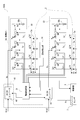
- FIG. 12 is an explanatory diagram of a configuration example for realizing voltage detection as an embodiment, and includes a light-emitting unit together with an internal configuration example of the drive unit 3 (particularly, an internal configuration example of the drive control unit 31) in the light source device 100. 2, a DC / DC converter 40, a control unit 9, and a temperature detection unit 10.
- the drive control unit 31 individually detects the voltages of the plurality of light emitting elements 2a in the light emitting unit 2 by time division.
- the drive control unit 31 includes a selector 33, a counter 34, a decoder 35, and an A / D converter 36.
- the drive control unit 31 includes a logic circuit 32 that performs ON / OFF control of each switch SW in the drive circuit 30.
- the logic circuit 32 is connected to the control unit 9, and is configured to be able to perform ON / OFF control of the light emitting element 2 a based on an instruction from the control unit 9. At this time, the logic circuit 32 synchronizes the ON timing and the OFF timing of each light emitting element 2 a with the frame cycle of the image sensor 7 based on the frame synchronization signal Fs supplied from the image sensor 7. Further, the logic circuit 32 can also perform ON / OFF control of the light emitting element 2a based on the temperature of the light emitting unit 2 detected by the temperature detecting unit 10.
- the selector 33 has at least as many input terminals as the number of the detection lines Ld, and each input terminal is connected to the anode of the corresponding light emitting element 2a via the corresponding detection line Ld.
- the selector 33 has a configuration in which, for example, a switch circuit such as a transfer gate circuit is provided for each detection line Ld.
- the clock CLK is input to the counter 34 from the logic circuit 32.
- the counter 34 starts the counting operation based on the clock CLK and starts outputting the count value CN obtained by the counting operation.
- the count value CN is supplied to the decoder 35 and the logic circuit 32, respectively.
- the decoder 35 instructs the selector 33 to select the detection line Ld according to the count value CN.
- the selector 33 outputs a voltage value obtained on a single detection line Ld specified by the decoder 35 among the detection lines Ld to the A / D converter 36 as an output value HDR.
- the A / D converter 36 digitally samples the input voltage value (analog value) and outputs the sampled voltage value (digital value) to the logic circuit 32.
- the logic circuit 32 based on the voltage value of the light emitting element 2a detected in a time-sharing manner by the selector 33, the counter 34, the decoder 35, and the A / D converter 36, the logic circuit 32 performs an abnormality related to the voltage of each light emitting element 2a. Make a judgment (voltage abnormality judgment).
- FIG. 13 is a diagram illustrating a relationship between a clock CLK used for time-division detection, an output value HDR (digital value) input to the logic circuit 32, and an abnormality detection signal Der generated internally by the logic circuit 32. .
- This figure illustrates a case where the number of the light emitting elements 2a is set to n of 7 or more.
- the number assigned to the output value HDR indicates the type of the light emitting element 2a to which the voltage value is input to the logic circuit 32 (in other words, the type of the detection line Ld selected by the selector 33).
- the error detection signal Der is generated as a signal that rises (or falls) when the output value HDR of the light-emitting element 2a is sequentially input as described above and an abnormality in the output value HDR is determined. Is done. In the figure, when the output value HDR of the fifth light emitting element 2a (the fifth light emitting element 2a whose voltage value is input to the logic circuit 32) is determined to be abnormal, an error is detected at the fifth timing. An example in which the signal Der is activated is shown.
- the determination of the presence or absence of the voltage abnormality of the light emitting element 2a is performed as a determination as to whether the output value HDR is a value within a predetermined range defined by an upper threshold THu and a lower threshold THd (THu> THd). . Accordingly, it is possible to appropriately determine whether or not there is a voltage abnormality in the light emitting element 2a due to a disconnection, a short circuit, a ground fault, or the like.
- the logic circuit 32 writes an error flag in the register. By writing the error flag in the register in this way, it is possible to notify, for example, the control unit 9 or the like that an abnormality has occurred in the light emitting unit 2.
- the count value CN is input from the counter 34 to the logic circuit 32.
- the logic circuit 32 specifies the light emitting element 2a to be detected based on the input count value CN. It is possible to do. In particular, when performing the above-described abnormality determination, it is possible to specify not only the presence or absence of the abnormality but also the light emitting element 2a in which the abnormality has occurred.
- the logic circuit 32 of the present example controls the output voltage Vo based on the output value HDR. Specifically, the logic circuit 32 determines whether or not the output value HDR input from the A / D converter 36 is equal to or more than a threshold value THe (however, THd ⁇ THe ⁇ THu), and if the output value HDR is equal to or more than the threshold value THe. In some cases, a power control signal for increasing the output voltage Vo is output to the DC / DC converter 40.
- each light emitting element 2a is performed based on a common power supply voltage (output voltage Vo) generated by a common power supply circuit (DC / DC converter 40).
- output voltage Vo output voltage generated by a common power supply circuit
- DC / DC converter 40 common power supply circuit
- the light emitting elements 2a vary in characteristics such as the forward voltage (VF) among the individual light emitting elements, in the case of a configuration in which a plurality of light emitting elements 2a are driven based on a common power supply voltage as in this example. It is important to adjust the height of the power supply voltage in accordance with the voltage of the light emitting element having a high detection voltage, in order to properly emit light from all the light emitting elements 2a to be emitted. Therefore, by performing the above-described power supply control, the height of the common power supply voltage is adjusted in accordance with the voltage of the light emitting element 2a having a high detection voltage. This makes it possible to appropriately emit light from all the light-emitting elements 2a to be emitted while reducing the circuit scale by employing a configuration in which the plurality of light-emitting elements 2a are driven based on a common power supply voltage.
- VF forward voltage
- FIG. 14 is a flowchart illustrating a specific processing procedure that the logic circuit 32 should perform in implementing the abnormality determination and power supply control described above.
- the logic circuit 32 performs a process of enabling the counter 34 by the enable signal EN as the counter start control process of step S101.
- the counter 34 is started, and voltage detection by time division is started.
- the timing for starting the voltage detection by such time division may be, for example, immediately before the start of the distance measurement, when the power is turned on, at regular intervals, or the like.
- the distance measuring device 1 is an information processing terminal such as a smartphone or a tablet terminal, for example, voltage detection may be started in response to sleep release.
- step S102 the logic circuit 32 determines whether the detected voltage value is within a predetermined range, that is, the output value HDR input from the A / D converter 36 is equal to or more than the lower threshold THd and equal to or less than the upper threshold THu. It is determined whether or not.
- step S102 when the output value HDR is equal to or more than the lower threshold THd and equal to or less than the upper threshold THu, and it is determined that the detected voltage value is within a predetermined range, the logic circuit 32 proceeds to step S103, and determines whether the detected voltage value is equal to the threshold value. It is determined whether the detected voltage value is equal to or higher than the threshold value THe.
- step S104 a process of outputting a power source control signal in step S104, that is, a DC / DC converter
- step S105 a confirmation process of the count value CN is performed in step S105.
- the logic circuit 32 passes the output process of step S104 and performs a check process of the count value CN in step S105.
- the logic circuit 32 determines whether the count value CN is equal to or greater than the maximum value CNmax.
- the maximum value CNmax is set to the same value as the number of light-emitting elements 2a to be subjected to voltage detection. If the count value CN is not equal to or greater than the maximum value CNmax in step S105, the logic circuit 32 waits until the count value CN is updated in step S106, and returns to the determination processing in step S102. As a result, the presence or absence of a voltage abnormality is determined for the next light emitting element 2a. If the count value CN is equal to or greater than the maximum value CNmax in step S105, the logic circuit 32 ends a series of processes illustrated in FIG.
- step S102 if the detected voltage value is not within the predetermined range (not more than the lower threshold value THd and not more than the upper threshold value THu), the logic circuit 32 proceeds to step S107, writes an error flag in a register, In step S108, a drive stop control process is executed, and a series of processes shown in FIG. In the drive stop control process in step S108, control is performed to stop the light emission drive of the light emitting element 2a, for example, stop the DC / DC converter 40.
- FIG. 15 is a diagram exemplifying an arrangement mode of each element constituting the driving unit 3 on a chip.
- the driving unit 3 can be mounted as a chip Cp3 (or a chip Cp34: the same in the following description of FIG. 15), and the chip Cp2 as the light emitting unit 2 is flip-chip mounted on the chip Cp3. (See, for example, FIG. 11).
- the drive circuit 30 (the drive element Q1 and the current control element Q2) in the drive section 3 can be arranged at a position directly below the chip Cp2 in the chip Cp3, as exemplified by a region p30 in the drawing.
- the selector 33 in the drive control unit 31 can be arranged in an area p33 adjacent to the area p30 in the chip Cp3, and the A / D converter 36 is an area adjacent to the area p33 on the opposite side to the area p30. p36.
- a logic circuit 32, a counter 34, a decoder 35, and the like can be arranged in an area p32 adjacent to the area p36 on the opposite side of the area p33.
- the heat source as the logic circuit 32 is separated from the heat sources as the light emitting unit 2 and the drive circuit 30, so that a rise in temperature can be suppressed.
- a configuration example using the counter 34 has been described as a configuration example for performing the time-division detection, but a configuration in which the counter 34 is omitted as in the drive control unit 31A illustrated in FIG. 16 may be employed. it can.
- the logic circuit 32 cannot specify the correspondence between the detected voltage value and the light emitting element 2a based on the count value CN.
- the logic circuit 32 scans and drives the plurality of light emitting elements 2a under the control of the switch SW, the logic circuit 32 can know which light emitting element 2a is emitting light. By controlling the decoder 35 so that the selector 33 selects the detection line Ld connected to the light emitting element 2a, it is possible to specify the correspondence between the detected voltage value and the light emitting element 2a.
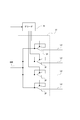
- each operational amplifier OP is provided for each detection line Ld, and each operational amplifier OP has a non-inverting terminal connected to the corresponding detecting line Ld, an inverting terminal connected to the output terminal, and a voltage follower.
- the connection point between the output terminal and the inversion terminal of each operational amplifier OP is connected to the output value HDR line.
- the decoder 35 controls the operational amplifiers OP to be in the ON state (enable) in order by performing ON / OFF control of each operational amplifier OP according to the count value CN of the counter 34 or an instruction from the logic circuit 32.
- the output value HDR of the selection circuit 37 is expressed by sequentially switching the voltage values of the plurality of light emitting elements 2a.
- the selection circuit 37 By using the selection circuit 37 as described above, not only the function as the selector 33 (that is, the time division selection function of the detection line Ld) but also the function of preventing the voltage drop in the detection line Ld can be provided.
- the voltage detection at the cathode of the light emitting element 2a as shown in FIG. A similar configuration can be adopted for power supply control based on this.
- the light source device includes a light emitting unit (2) in which a plurality of light emitting elements (2a) are arranged by a vertical cavity surface emitting laser, and a plurality of light emission in the light emitting unit.
- a detection unit (selector 33 or selection circuit 37, decoder 35, and A / D converter 36) for individually detecting the voltage at the anode or the cathode of the element by time division.
- the circuit scale for voltage detection can be reduced, and in a light source device including a light emitting unit in which a plurality of light emitting elements by a vertical cavity surface emitting laser are arranged, it is possible to separately detect a voltage for each light emitting element. Thus, the size of the apparatus can be reduced.
- the detection unit has a counter (No. 34) that switches the light-emitting element to be detected in accordance with the clock and counts in synchronization with the clock.
- the detection unit includes a voltage detection line (the same Ld) for each light emitting element, and a voltage follower (op-amp OP) inserted for each detection line and configured to be capable of ON / OFF control.
- the light source device includes a drive circuit (30 or 30 A in the present embodiment) that supplies a drive current to a plurality of light emitting elements by a current mirror circuit.
- the current mirror circuit is connected to the anode side of the light emitting element, and the detection unit detects the voltage at the anode of the light emitting element (see FIG. 12 and the like).
- the current mirror circuit is connected to the cathode side of the light emitting element, and the detection unit detects the voltage at the cathode of the light emitting element.
- the light source device further includes a determination unit (logic circuit 32) that determines an abnormality of the light emitting element based on the voltage individually detected by the detection unit.
- a determination unit logic circuit 32 that determines an abnormality of the light emitting element based on the voltage individually detected by the detection unit.
- the determination unit determines whether or not the voltage value is within a predetermined range as the determination as to whether the light emitting element is abnormal.
- the control unit controls the power supply circuit to increase the power supply voltage in response to the detection unit detecting a voltage equal to or higher than a predetermined threshold (threshold THe).
- the height of the common power supply voltage is adjusted in accordance with the voltage of the light emitting element having a high detection voltage. Is made possible. Therefore, all the light-emitting elements to be light-emitting can emit light appropriately without employing a configuration in which the power supply voltage can be adjusted for each light-emitting element. That is, all the light-emitting elements sharing the power supply voltage can emit light appropriately, while preventing an increase in circuit scale when the power supply voltage is adjustable for each light-emitting element.
- the light source device includes a drive circuit (30 or 30A) having a switch (SW) provided for each light emitting element and configured to individually drive the light emitting elements in the light emitting section. I have.
- the light emitting section makes it possible for the light emitting section to emit light in an arbitrary light emitting pattern (two-dimensional light / dark pattern). Therefore, when it is required to make the light emission pattern variable for the light emission for distance measurement, it is not necessary to provide a plurality of light emission portions having a fixed light emission pattern, and the number of components and the size of the light source device can be reduced. . Further, when the light emitting element is configured to be individually drivable, the drive control unit of the light emitting element can grasp the light emitting element that is being driven (emitting light). When the value is equal to or more than the predetermined value, it is possible to determine that the wiring is short-circuited with the wiring of another light emitting element that is emitting light.
- the detection method according to the embodiment is a detection method in which voltages at anodes or cathodes of a plurality of light emitting elements in a light emitting unit in which a plurality of light emitting elements by a vertical cavity surface emitting laser are arranged are time-divisionally individually.
- the sensing module according to the embodiment includes a light source device according to the above-described embodiment and an image sensor configured to receive light reflected from a subject emitted from a light emitting unit (2) included in the light source device and image the received light. 7) (for example, see the configuration shown in FIG. 8).
- a light emitting unit in which a plurality of light emitting elements by a vertical cavity surface emitting laser are arranged A light-emitting device comprising: a detection unit configured to individually detect voltages at anodes or cathodes of the plurality of light-emitting elements in the light-emitting unit by time division.
- the detection unit While switching the light emitting element to be detected according to the clock, The light source device according to (1), further including a counter that counts in synchronization with the clock.
- the detection unit A detection line for the voltage for each light emitting element;
- the light source device according to (1) or (2) further including a voltage follower inserted for each of the detection lines and configured to be capable of ON / OFF control.
- the light source device according to any one of (1) to (3) further including: a driving circuit configured to supply a driving current to the plurality of light emitting elements by a current mirror circuit.
- the current mirror circuit is connected to an anode side of the light emitting element, The detection unit, The light source device according to (4), wherein a voltage at an anode of the light emitting element is detected.
- the current mirror circuit is connected to a cathode side of the light emitting element, The detection unit, The light source device according to (4), wherein a voltage at a cathode of the light emitting element is detected.
- the determination unit includes: The light source device according to (7), wherein determining whether the value of the voltage is within a predetermined range is performed as determining whether the light emitting element is abnormal.
- a power supply circuit for generating a power supply voltage commonly used for driving a plurality of the light emitting elements The light source device according to any one of (1) to (8), further including: a control unit configured to control the power supply circuit based on the voltage detected by the detection unit.
- the control unit includes: The light source device according to (9), wherein the power supply circuit is controlled to increase the power supply voltage in response to the detection unit detecting the voltage equal to or higher than a predetermined threshold.
- the light source device according to any one of (1) to (10) further including a drive circuit including a switch provided for each of the light emitting elements and configured to individually drive the light emitting elements in the light emitting unit.
- 1 distance measuring device 2 light emitting unit, 2a light emitting element, 3, 3A driving unit, 7 image sensor, 10 temperature detecting unit, S subject, B substrate, Cp2, Cp3, Cp4, Cp34, Cp7 chip, 30, 30A driving circuit , 31, 31A drive control section, Q1 drive element, Q2 current control element, SW switch, 32 logic circuit, 33 selector, 34 counter, 35 decoder, 36 A / D converter, 37 select circuit, 100, 100A light source device
Landscapes
- Physics & Mathematics (AREA)
- Engineering & Computer Science (AREA)
- General Physics & Mathematics (AREA)
- Electromagnetism (AREA)
- Computer Networks & Wireless Communication (AREA)
- Radar, Positioning & Navigation (AREA)
- Remote Sensing (AREA)
- Condensed Matter Physics & Semiconductors (AREA)
- Optics & Photonics (AREA)
- Computer Vision & Pattern Recognition (AREA)
- Semiconductor Lasers (AREA)
- Optical Radar Systems And Details Thereof (AREA)
Abstract
垂直共振器面発光レーザによる発光素子が複数配列された発光部を備えた光源装置について、発光素子ごとに電圧を検出し分けることを可能としながら装置サイズの小型化を図る。 本技術に係る光源装置は、垂直共振器面発光レーザによる発光素子が複数配列された発光部と、発光部における複数の発光素子のアノード又はカソードにおける電圧を時分割により個別検出する検出部とを備える。これにより、発光素子ごとに電圧検出のための回路を設ける必要がなくなり、装置サイズの小型化を図ることができる。
Description
本技術は、垂直共振器面発光レーザによる発光素子が複数配列された発光部を備えた光源装置と、それら発光素子の電圧を検出する検出方法と、前記発光部より発せられ被写体によって反射された光を受光して撮像するイメージセンサを備えたセンシングモジュールとに関する。
レーザ光を発する発光素子として、VCSEL(Vertical Cavity Surface Emitting LASER:垂直共振器面発光レーザ)としての発光素子が知られている(例えば下記特許文献1、2を参照)。
VCSELとしての発光素子は、共振器が半導体の基板面に対して垂直方向に形成されて、レーザ光を垂直方向に出射するように構成され、近年においては、例えばSTL(Structured Light:構造化光)方式やToF(Time of Flight:光飛行時間)方式による被写体の測距を行う際の光源として広く用いられる。
VCSELとしての発光素子は、共振器が半導体の基板面に対して垂直方向に形成されて、レーザ光を垂直方向に出射するように構成され、近年においては、例えばSTL(Structured Light:構造化光)方式やToF(Time of Flight:光飛行時間)方式による被写体の測距を行う際の光源として広く用いられる。
ここで、被写体の測距としてSTL方式やToF方式による測距を行う場合は、VCSELとしての発光素子を二次元に複数配列した光源装置が用いられる。具体的には、それら複数の発光素子を発光させて得られる光を被写体に照射し、被写体からの反射光を受光して得られる画像に基づいて被写体の測距が行われる。
ここで、発光素子を適切に発光させる上では、発光素子に生じる電圧を検出して電源電圧を制御したり回路を停止させることが有効である。また、安全性を高める上では、発光素子の電圧異常を検知して電源電圧を制御することが有効である。
しかしながら、発光素子ごとに電圧検出のための回路を設けることは回路規模の拡大化を招き、光源装置の小型化が困難となるため望ましくない。
本技術は上記の事情に鑑み為されたものであり、垂直共振器面発光レーザによる発光素子が複数配列された発光部を備えた光源装置について、発光素子ごとに電圧を検出し分けることを可能としながら装置サイズの小型化を図ることを目的とする。
本技術に係る光源装置は、垂直共振器面発光レーザによる発光素子が複数配列された発光部と、前記発光部における複数の前記発光素子のアノード又はカソードにおける電圧を時分割により個別検出する検出部とを備えるものである。
これにより、発光素子ごとに電圧検出のための回路を設ける必要がなくなる。
上記した本技術に係る光源装置においては、前記検出部は、クロックに従って検出対象とする前記発光素子を切り替えると共に、前記クロックに同期して計数を行うカウンタを有することが望ましい。
カウンタの計数値により、検出した電圧値が何れの発光素子の電圧値であるかを特定可能とされる。
上記した本技術に係る光源装置においては、前記検出部は、前記発光素子ごとの前記電圧の検出ラインと、前記検出ラインごとに挿入されON/OFF制御可能に構成されたボルテージフォロアとを有することが望ましい。
これにより、検出ラインの時分割選択機能のみでなく検出ラインにおける電圧低下防止機能を兼ね備えることが可能とされる。
上記した本技術に係る光源装置においては、カレントミラー回路により複数の前記発光素子に駆動電流を流す駆動回路を備えたことが望ましい。
これにより、発光素子に定電流を流すにあたって定電流制御機能付の電源回路を用いる必要がなくなる。
上記した本技術に係る光源装置においては、前記カレントミラー回路が前記発光素子のアノード側に接続され、前記検出部は、前記発光素子のアノードにおける電圧を検出することが望ましい。
これにより、発光素子、及びカレントミラー回路における駆動素子それぞれの特性個体差を考慮した適切な電圧検出を行うことが可能とされる。
上記した本技術に係る光源装置においては、前記カレントミラー回路が前記発光素子のカソード側に接続され、前記検出部は、前記発光素子のカソードにおける電圧を検出することが望ましい。
これにより、発光素子、及びカレントミラー回路における駆動素子それぞれの特性個体差を考慮した適切な電圧検出を行うことが可能とされる。
上記した本技術に係る光源装置においては、前記検出部が前記個別検出した電圧に基づき前記発光素子の異常判定を行う判定部を備えたことが望ましい。
これにより、発光素子ごとに電圧異常検出のための回路を設ける必要がなくなる。
上記した本技術に係る光源装置においては、前記判定部は、前記電圧の値が所定範囲内の値であるか否かの判定を前記発光素子の異常有無の判定として行うことが望ましい。
これにより、断線、短絡、地絡等に起因した発光素子の電圧異常の有無を適切に判定することが可能とされる。
上記した本技術に係る光源装置においては、複数の前記発光素子の駆動に共通に用いられる電源電圧を生成する電源回路と、前記検出部が検出した前記電圧に基づいて前記電源回路を制御する制御部と、を備えたことが望ましい。
これにより、共通の電源回路が生成する共通の電源電圧に基づき複数の発光素子が駆動される構成において、例えば発光素子の電圧異常が認められた場合は電源回路の動作を停止させる等して安全性を高めたり、また検出電圧が高い発光素子に合わせて電源電圧の高さを調整することで発光対象とする全ての発光素子を適切に発光させる等の電源制御を行うことが可能とされる。
上記した本技術に係る光源装置においては、前記制御部は、前記検出部が所定閾値以上の前記電圧を検出したことに応じて前記電源電圧を高めるように前記電源回路を制御することが望ましい。
これにより、共通の電源回路が生成する共通の電源電圧に基づき複数の発光素子が駆動される構成において、該共通の電源電圧の高さを検出電圧が高い発光素子の電圧に合わせて調整することが可能とされる。
上記した本技術に係る光源装置においては、前記発光素子ごとに設けられたスイッチを有し前記発光部における前記発光素子を個別駆動可能に構成された駆動回路を備えたことが望ましい。
これにより、発光部を任意の発光パターン(二次元の明暗パターン)により発光させることが可能とされる。
また、本技術に係る検出方法は、垂直共振器面発光レーザによる発光素子が複数配列された発光部における複数の前記発光素子のアノード又はカソードにおける電圧を時分割により個別検出する検出方法である。
さらに、本技術に係るセンシングモジュールは、上記した本技術に係る光源装置と、該光源装置が備える発光部より発せられ被写体によって反射された光を受光して撮像するイメージセンサとを備えるものである。
さらに、本技術に係るセンシングモジュールは、上記した本技術に係る光源装置と、該光源装置が備える発光部より発せられ被写体によって反射された光を受光して撮像するイメージセンサとを備えるものである。
このような検出方法やセンシングモジュールによっても、上記した本技術に係る光源装置と同様の作用が得られる。
本技術によれば、垂直共振器面発光レーザによる発光素子が複数配列された発光部を備えた光源装置について、発光素子ごとに電圧を検出し分けることを可能としながら装置サイズの小型化を図ることができる。
なお、ここに記載された効果は必ずしも限定されるものではなく、本開示中に記載されたいずれかの効果であってもよい。
なお、ここに記載された効果は必ずしも限定されるものではなく、本開示中に記載されたいずれかの効果であってもよい。
以下、添付図面を参照し、本技術に係る実施形態を次の順序で説明する。
<1.測距装置の構成>
<2.測距手法について>
<3.発光駆動に係る回路構成について>
<4.基板構成のバリエーション>
<5.VCSELの構造例>
<6.実施形態としての電圧検出及び制御>
<7.実施形態のまとめ及び変形例>
<8.本技術>
<1.測距装置の構成>
<2.測距手法について>
<3.発光駆動に係る回路構成について>
<4.基板構成のバリエーション>
<5.VCSELの構造例>
<6.実施形態としての電圧検出及び制御>
<7.実施形態のまとめ及び変形例>
<8.本技術>
<1.測距装置の構成>
図1は、本技術に係る光源装置の一実施形態としての測距装置1の構成例を示している。
図示のように測距装置1は、発光部2、駆動部3、電源回路4、発光側光学系5、撮像側光学系6、イメージセンサ7、画像処理部8、制御部9、及び温度検出部10を備えている。
発光部2は、複数の光源により光を発する。後述するように、本例の発光部2は、各光源としてVCSEL(Vertical Cavity Surface Emitting LASER:垂直共振器面発光レーザ)による発光素子2aを有しており、それら発光素子2aが例えばマトリクス状等の所定態様により配列されて構成されている。
図1は、本技術に係る光源装置の一実施形態としての測距装置1の構成例を示している。
図示のように測距装置1は、発光部2、駆動部3、電源回路4、発光側光学系5、撮像側光学系6、イメージセンサ7、画像処理部8、制御部9、及び温度検出部10を備えている。
発光部2は、複数の光源により光を発する。後述するように、本例の発光部2は、各光源としてVCSEL(Vertical Cavity Surface Emitting LASER:垂直共振器面発光レーザ)による発光素子2aを有しており、それら発光素子2aが例えばマトリクス状等の所定態様により配列されて構成されている。
駆動部3は、発光部2を駆動するための電気回路を有して構成される。
電源回路4は、例えば測距装置1に設けられた不図示のバッテリ等からの入力電圧(後述する入力電圧Vin)に基づき、駆動部3の電源電圧(後述する出力電圧Vo)を生成する。駆動部3は、該電源電圧に基づいて発光部2を駆動する。
電源回路4は、例えば測距装置1に設けられた不図示のバッテリ等からの入力電圧(後述する入力電圧Vin)に基づき、駆動部3の電源電圧(後述する出力電圧Vo)を生成する。駆動部3は、該電源電圧に基づいて発光部2を駆動する。
発光部2より発せられた光は、発光側光学系5を介して測距対象としての被写体Sに照射される。そして、このように照射された光の被写体Sからの反射光は、撮像側光学系6を介してイメージセンサ7の撮像面に入射する。
イメージセンサ7は、例えばCCD(Charge Coupled Device)センサやCMOS(Complementary Metal Oxide Semiconductor)センサ等の撮像素子とされ、上記のように撮像側光学系6を介して入射する被写体Sからの反射光を受光し、電気信号に変換して出力する。
イメージセンサ7は、受光した光を光電変換して得た電気信号について、例えばCDS(Correlated Double Sampling)処理、AGC(Automatic Gain Control)処理などを実行し、さらにA/D(Analog/Digital)変換処理を行う。そしてデジタルデータとしての画像信号を、後段の画像処理部8に出力する。
また、本例のイメージセンサ7は、フレーム同期信号Fsを駆動部3に出力する。これにより駆動部3は、発光部2における発光素子2aをイメージセンサ7のフレーム周期に応じたタイミングで発光させることが可能とされる。
イメージセンサ7は、受光した光を光電変換して得た電気信号について、例えばCDS(Correlated Double Sampling)処理、AGC(Automatic Gain Control)処理などを実行し、さらにA/D(Analog/Digital)変換処理を行う。そしてデジタルデータとしての画像信号を、後段の画像処理部8に出力する。
また、本例のイメージセンサ7は、フレーム同期信号Fsを駆動部3に出力する。これにより駆動部3は、発光部2における発光素子2aをイメージセンサ7のフレーム周期に応じたタイミングで発光させることが可能とされる。
画像処理部8は、例えばDSP(Digital Signal Processor)等により画像処理プロセッサとして構成される。画像処理部8は、イメージセンサ7から入力されるデジタル信号(画像信号)に対して、各種の画像信号処理を施す。
制御部9は、例えばCPU(Central Processing Unit)、ROM(Read Only Memory)、RAM(Random Access Memory)等を有するマイクロコンピュータ、或いはDSP等の情報処理装置を備えて構成され、発光部2による発光動作を制御するための駆動部3の制御や、イメージセンサ7による撮像動作に係る制御を行う。
制御部9は、測距部9aとしての機能を有する。測距部9aは、画像処理部8を介して入力される画像信号(つまり被写体Sからの反射光を受光して得られる画像信号)に基づき、被写体Sまでの距離を測定する。本例の測距部9aは、被写体Sの三次元形状の特定を可能とするために、被写体Sの各部について距離の測定を行う
ここで、測距装置1における具体的な測距の手法については後に改めて説明する。
ここで、測距装置1における具体的な測距の手法については後に改めて説明する。
温度検出部10は、発光部2の温度を検出する。温度検出部10としては、例えばダイオードを用いて温度検出を行う構成を採ることができる。
本例では、温度検出部10により検出された温度の情報は駆動部3に供給され、これにより駆動部3は該温度の情報に基づいて発光部2の駆動を行うことが可能とされる。
本例では、温度検出部10により検出された温度の情報は駆動部3に供給され、これにより駆動部3は該温度の情報に基づいて発光部2の駆動を行うことが可能とされる。
<2.測距手法について>
測距装置1における測距手法としては、例えばSTL(Structured Light:構造化光)方式やToF(Time of Flight:光飛行時間)方式による測距手法を採用することができる。
STL方式は、例えばドットパターンや格子パターン等の所定の明暗パターンを有する光を照射された被写体Sを撮像して得られる画像に基づいて距離を測定する方式である。
図2は、STL方式の説明図である。
STL方式では、例えば図2Aに示すようなドットパターンによるパターン光Lpを被写体Sに照射する。パターン光Lpは、複数のブロックBLに分割されており、各ブロックBLにはそれぞれ異なるドットパターンが割当てられている(ブロックBL間でドットパターンが重複しないようにされている)。
図2Bは、STL方式の測距原理についての説明図である。
ここでは、壁Wとその前に配置された箱BXとが被写体Sとされ、該被写体Sに対してパターン光Lpが照射された例としている。図中の「G」はイメージセンサ7による画角を模式的に表している。
また、図中の「BLn」はパターン光Lpにおける或るブロックBLの光を意味し、「dn」はイメージセンサ7による撮像画像に映し出されるブロックBLnのドットパターンを意味している。
ここで、壁Wの前の箱BXが存在しない場合、撮像画像においてブロックBLnのドットパターンは図中の「dn’」の位置に映し出される。すなわち、箱BXが存在する場合と箱BXが存在しない場合とで、撮像画像においてブロックBLnのパターンが映し出される位置が異なるものであり、具体的には、パターンの歪みが生じる。
測距装置1における測距手法としては、例えばSTL(Structured Light:構造化光)方式やToF(Time of Flight:光飛行時間)方式による測距手法を採用することができる。
STL方式は、例えばドットパターンや格子パターン等の所定の明暗パターンを有する光を照射された被写体Sを撮像して得られる画像に基づいて距離を測定する方式である。
図2は、STL方式の説明図である。
STL方式では、例えば図2Aに示すようなドットパターンによるパターン光Lpを被写体Sに照射する。パターン光Lpは、複数のブロックBLに分割されており、各ブロックBLにはそれぞれ異なるドットパターンが割当てられている(ブロックBL間でドットパターンが重複しないようにされている)。
図2Bは、STL方式の測距原理についての説明図である。
ここでは、壁Wとその前に配置された箱BXとが被写体Sとされ、該被写体Sに対してパターン光Lpが照射された例としている。図中の「G」はイメージセンサ7による画角を模式的に表している。
また、図中の「BLn」はパターン光Lpにおける或るブロックBLの光を意味し、「dn」はイメージセンサ7による撮像画像に映し出されるブロックBLnのドットパターンを意味している。
ここで、壁Wの前の箱BXが存在しない場合、撮像画像においてブロックBLnのドットパターンは図中の「dn’」の位置に映し出される。すなわち、箱BXが存在する場合と箱BXが存在しない場合とで、撮像画像においてブロックBLnのパターンが映し出される位置が異なるものであり、具体的には、パターンの歪みが生じる。
STL方式は、このように照射したパターンが被写体Sの物体形状によって歪むことを利用して被写体Sの形状や奥行きを求める方式となる。具体的には、パターンの歪み方から被写体Sの形状や奥行きを求める方式である。
STL方式を採用する場合、イメージセンサ7としては、例えばグローバルシャッタ方式によるIR(Infrared:赤外線)イメージセンサが用いられる。そして、STL方式の場合、測距部9aは、発光部2がパターン光を発光するように駆動部3を制御すると共に、画像処理部8を介して得られる画像信号についてパターンの歪みを検出し、パターンの歪み方に基づいて距離を計算する。
続いて、ToF方式は、発光部2より発された光が対象物で反射されてイメージセンサ7に到達するまでの光の飛行時間(時間差)を検出することで、対象物までの距離を測定する方式である。
ToF方式として、いわゆるダイレクトToF方式を採用する場合、イメージセンサ7としてはSPAD(Single Photon Avalanche Diode)を用い、また発光部2はパルス駆動する。この場合、測距部9aは、画像処理部8を介して入力される画像信号に基づき、発光部2より発せられイメージセンサ7により受光される光について発光から受光までの時間差を計算し、該時間差と光の速度とに基づいて被写体Sの各部の距離を計算する。
なお、ToF方式として、いわゆるインダイレクトToF方式(位相差法)を採用する場合、イメージセンサ7としては例えばIRイメージセンサが用いられる。
ToF方式として、いわゆるダイレクトToF方式を採用する場合、イメージセンサ7としてはSPAD(Single Photon Avalanche Diode)を用い、また発光部2はパルス駆動する。この場合、測距部9aは、画像処理部8を介して入力される画像信号に基づき、発光部2より発せられイメージセンサ7により受光される光について発光から受光までの時間差を計算し、該時間差と光の速度とに基づいて被写体Sの各部の距離を計算する。
なお、ToF方式として、いわゆるインダイレクトToF方式(位相差法)を採用する場合、イメージセンサ7としては例えばIRイメージセンサが用いられる。
<3.発光駆動に係る回路構成について>
図3は、図1に示した発光部2と駆動部3と電源回路4とを有して構成された光源装置100の回路構成例を示している。なお、図3では光源装置100の回路構成例と共に、図1に示したイメージセンサ7と制御部9を併せて示している。
本例では、発光部2と駆動部3と電源回路4は共通の基板(後述する基板B)上に形成されている。ここでは、少なくとも発光部2を含み、発光部2と共通の基板上に形成される構成単位を光源装置100と呼んでいる。
図3は、図1に示した発光部2と駆動部3と電源回路4とを有して構成された光源装置100の回路構成例を示している。なお、図3では光源装置100の回路構成例と共に、図1に示したイメージセンサ7と制御部9を併せて示している。
本例では、発光部2と駆動部3と電源回路4は共通の基板(後述する基板B)上に形成されている。ここでは、少なくとも発光部2を含み、発光部2と共通の基板上に形成される構成単位を光源装置100と呼んでいる。
図示のように光源装置100は、発光部2と駆動部3と電源回路4と共に温度検出部10を備えている。
発光部2は、前述したようにVCSELとしての発光素子2aを複数備えている。図3では図示の都合から発光素子2aの数を「4」としているが、発光部2における発光素子2aの数はこれに限らず、少なくとも2以上とされればよい。
発光部2は、前述したようにVCSELとしての発光素子2aを複数備えている。図3では図示の都合から発光素子2aの数を「4」としているが、発光部2における発光素子2aの数はこれに限らず、少なくとも2以上とされればよい。
電源回路4は、DC/DCコンバータ40を備え、直流電圧による入力電圧Vinに基づき、直流電圧による出力電圧Voを生成する。この出力電圧Voは、駆動部3が発光部2を駆動するための電源電圧として用いられる。
本例では、DC/DCコンバータ40は出力電圧Voの高さ(電流値)を調整可能に構成されている。
本例では、DC/DCコンバータ40は出力電圧Voの高さ(電流値)を調整可能に構成されている。
駆動部3は、駆動回路30と駆動制御部31とを備えている。
駆動回路30は、発光素子2aごとに駆動素子Q1及びスイッチSWを有すると共に、電流制御素子Q2と定電流源30aとを有している。
駆動素子Q1及び電流制御素子Q2にはFET(field-effect transistor)が用いられ、本例ではPチャンネル型のMOSFET(MOS:metal-oxide-semiconductor)が用いられている。
駆動回路30は、発光素子2aごとに駆動素子Q1及びスイッチSWを有すると共に、電流制御素子Q2と定電流源30aとを有している。
駆動素子Q1及び電流制御素子Q2にはFET(field-effect transistor)が用いられ、本例ではPチャンネル型のMOSFET(MOS:metal-oxide-semiconductor)が用いられている。
各駆動素子Q1は、DC/DCコンバータ40の出力ライン、すなわち出力電圧Voの供給ラインに対して並列の関係に接続され、電流制御素子Q2は、駆動素子Q1に対して並列接続されている。
具体的に、各駆動素子Q1及び電流制御素子Q2は、ソースがDC/DCコンバータ40の出力ラインに接続されている。各駆動素子Q1のドレインは、発光部2における発光素子2aのうちそれぞれ対応する一つの発光素子2aのアノードと接続されている。
図示のように各発光素子2aのカソードはグランド(GND)に接続されている。
具体的に、各駆動素子Q1及び電流制御素子Q2は、ソースがDC/DCコンバータ40の出力ラインに接続されている。各駆動素子Q1のドレインは、発光部2における発光素子2aのうちそれぞれ対応する一つの発光素子2aのアノードと接続されている。
図示のように各発光素子2aのカソードはグランド(GND)に接続されている。
電流制御素子Q2は、ドレインが定電流源30aを介してグランドに接続され、ゲートがドレインと定電流源30aとの接続点に接続されている。
各駆動素子Q1のゲートは、それぞれ対応する一つのスイッチSWを介して電流制御素子Q2のゲートに接続されている。
各駆動素子Q1のゲートは、それぞれ対応する一つのスイッチSWを介して電流制御素子Q2のゲートに接続されている。
上記構成による駆動回路30においては、スイッチSWがONとされた駆動素子Q1が導通し、導通した駆動素子Q1に接続された発光素子2aに出力電圧Voに基づく駆動電圧Vdが印加され、該発光素子2aが発光する。
このとき、発光素子2aには駆動電流Idが流れるが、上記構成による駆動回路30においては駆動素子Q1と電流制御素子Q2がカレントミラー回路を構成しており、駆動電流Idの電流値は定電流源30aの電流値に応じた値に制御される。
駆動制御部31は、駆動回路30におけるスイッチSWのON/OFF制御を行うことで、発光素子2aのON/OFFを制御する。図中では、駆動制御部31が各スイッチSWを個別にON/OFF制御するための制御信号ラインをそれぞれ制御信号ラインLsと表記している。
駆動制御部31にはイメージセンサ7よりフレーム同期信号Fsが供給されており、これにより駆動制御部31は発光素子2aのONタイミングやOFFタイミングをイメージセンサ7のフレーム周期に同期させることが可能とされている。
また、駆動制御部31は、発光素子2aのON/OFF制御を制御部9からの指示に基づき行うことが可能に構成されている。
駆動制御部31にはイメージセンサ7よりフレーム同期信号Fsが供給されており、これにより駆動制御部31は発光素子2aのONタイミングやOFFタイミングをイメージセンサ7のフレーム周期に同期させることが可能とされている。
また、駆動制御部31は、発光素子2aのON/OFF制御を制御部9からの指示に基づき行うことが可能に構成されている。
また、駆動制御部31は、温度検出部10により検出された発光部2の温度に基づき発光素子2aのON/OFF制御を行うことも可能とされている。
さらに、駆動制御部31は、電源回路4におけるDC/DCコンバータ40に対する指示を行って出力電圧Voを調整させることが可能とされるが、これについては後に改めて説明する。
さらに、駆動制御部31は、電源回路4におけるDC/DCコンバータ40に対する指示を行って出力電圧Voを調整させることが可能とされるが、これについては後に改めて説明する。
図示のように駆動部3には、発光素子2aごとに、発光素子2aに生じる電圧を検出するための検出ラインLdが形成されている。具体的に、図3に示す構成においては、各検出ラインLdはそれぞれが対応する発光素子2aのアノードに接続されている。
本例の駆動制御部31には、各検出ラインLdに得られる電圧、すなわち発光素子2aごとの電圧を個別に検出するための構成が設けられているが、これについては後に改めて説明する。
本例の駆動制御部31には、各検出ラインLdに得られる電圧、すなわち発光素子2aごとの電圧を個別に検出するための構成が設けられているが、これについては後に改めて説明する。
ここで、図3では、駆動素子Q1と電流制御素子Q2によるカレントミラー回路を発光素子2aのアノード側に設けた構成を例示したが、図4に示す駆動回路30Aのように、カレントミラー回路を発光素子2aのカソード側に設けた構成とすることもできる。
この場合、発光部2における各発光素子2aは、アノードがDC/DCコンバータ40の出力ラインに接続されている。
この場合、カレントミラー回路を構成する駆動素子Q1及び電流制御素子Q2には、Nチャンネル型のMOSFETが用いられる。電流制御素子Q2は、ドレイン及びゲートが定電流源30aを介してDC/DCコンバータ40の出力ラインに接続され、ソースはグランドに接続される。
各駆動素子Q1は、ドレインが対応する発光素子2aのカソードに接続され、ソースがグランドに接続される。各駆動素子Q1のゲートは、それぞれ対応するスイッチSWを介して電流制御素子Q2のゲートとドレインに接続される。
この場合、発光部2における各発光素子2aは、アノードがDC/DCコンバータ40の出力ラインに接続されている。
この場合、カレントミラー回路を構成する駆動素子Q1及び電流制御素子Q2には、Nチャンネル型のMOSFETが用いられる。電流制御素子Q2は、ドレイン及びゲートが定電流源30aを介してDC/DCコンバータ40の出力ラインに接続され、ソースはグランドに接続される。
各駆動素子Q1は、ドレインが対応する発光素子2aのカソードに接続され、ソースがグランドに接続される。各駆動素子Q1のゲートは、それぞれ対応するスイッチSWを介して電流制御素子Q2のゲートとドレインに接続される。
この場合も駆動制御部31がスイッチSWのON/OFF制御を行うことで、発光素子2aをON/OFFさせることができる。
また、この場合は、カレントミラー回路が発光素子2aのカソード側に接続されたことに対応して、各検出ラインLdは、それぞれ対応する発光素子2aのカソードに対して接続されている。すなわち、この場合の駆動制御部31は、発光素子2aのカソードにおける電圧を検出する。
図5は、変形例としての光源装置100Aの構成例を示している。
光源装置100Aは、電源回路4に代えて電源回路4Aが設けられ、また駆動部3に代えて駆動部3Aが設けられた点が光源装置100と異なる。
電源回路4Aは、複数のDC/DCコンバータ40を有する(図の例では二つ)。一方のDC/DCコンバータ40には入力電圧Vin1が、他方のDC/DCコンバータ40には入力電圧Vin2が供給される。駆動部3Aは、それぞれが異なるDC/DCコンバータ40から出力電圧Voを入力する複数の駆動回路30を備えている。図示のように各駆動回路30においては、定電流源30aに代えて可変電流源30bが設けられている。可変電流源30bは、電流値が可変の電流源とされる。
この場合、発光部2における発光素子2aは、それぞれON/OFF制御される駆動回路30が異なる複数の発光素子群に分けられる。
この場合の駆動制御部31は、各駆動回路30におけるスイッチSWのON/OFF制御を行う。
光源装置100Aは、電源回路4に代えて電源回路4Aが設けられ、また駆動部3に代えて駆動部3Aが設けられた点が光源装置100と異なる。
電源回路4Aは、複数のDC/DCコンバータ40を有する(図の例では二つ)。一方のDC/DCコンバータ40には入力電圧Vin1が、他方のDC/DCコンバータ40には入力電圧Vin2が供給される。駆動部3Aは、それぞれが異なるDC/DCコンバータ40から出力電圧Voを入力する複数の駆動回路30を備えている。図示のように各駆動回路30においては、定電流源30aに代えて可変電流源30bが設けられている。可変電流源30bは、電流値が可変の電流源とされる。
この場合、発光部2における発光素子2aは、それぞれON/OFF制御される駆動回路30が異なる複数の発光素子群に分けられる。
この場合の駆動制御部31は、各駆動回路30におけるスイッチSWのON/OFF制御を行う。
なお、図5では図示の都合から検出ラインLdを省略しているが、この場合、各検出ラインLdは、駆動素子Q1と電流制御素子Q2によるカレントミラー回路が発光素子2aのアノード側に接続されていることから、それぞれ対応する発光素子2aのアノードに接続する。すなわち、この場合の駆動制御部31は、発光素子2aのアノードにおける電圧を検出する。
図5に示す光源装置100Aのように、少なくともDC/DCコンバータ40と駆動回路30の組を複数系統に分けた構成とすることで、系統ごとに発光素子2aの駆動電流Idを異なる値とすることができる。例えば、系統ごとに出力電圧Voの電圧値、及び可変電流源30bの電流値を異ならせることで、系統ごとに駆動電流Idの値を異ならせることができる。また、DC/DCコンバータ40が駆動電流Idについて定電流制御を行う構成であれば、各DC/DCコンバータ40間でそれぞれ定電流制御の目標値を異ならせることで、系統ごとに駆動電流Idの値を異ならせることもできる。
図5のような構成を採る場合には、発光部2における発光強度分布や温度分布等に応じて系統ごとに出力電圧Voや駆動電流Idの値を異ならせることが考えられる。例えば、発光部2における温度が高い箇所に対応した系統について駆動電流Idを増やし且つ出力電圧Voを上げる等が考えられる。
<4.基板構成のバリエーション>
ここで、光源装置100としては、図6乃至図8に示す構成とすることができる。
光源装置100としては、図6Aに示すように、発光部2としての回路が形成されたチップCp2と、駆動部3としての回路が形成されたチップCp3と、電源回路4が形成されたチップCp4とを同一の基板B上に形成した構成とすることができる。
また、駆動部3と電源回路4は、同一のチップCp34に形成することもでき、その場合、光源装置100は、図6Bに示すようにチップCp2とチップCp34とを同一の基板B上に形成した構成とすることもできる。
ここで、光源装置100としては、図6乃至図8に示す構成とすることができる。
光源装置100としては、図6Aに示すように、発光部2としての回路が形成されたチップCp2と、駆動部3としての回路が形成されたチップCp3と、電源回路4が形成されたチップCp4とを同一の基板B上に形成した構成とすることができる。
また、駆動部3と電源回路4は、同一のチップCp34に形成することもでき、その場合、光源装置100は、図6Bに示すようにチップCp2とチップCp34とを同一の基板B上に形成した構成とすることもできる。
また、チップCpに対して他のチップCpを搭載した構成とすることもできる。
その場合、光源装置100としては、例えば図7Aのように、チップCp2を搭載したチップCp3とチップCp4とを基板B上に形成した構成や、図7BのようにチップCp2とチップCp4とを搭載したチップCp3を基板B上に形成した構成、或いは、図7CのようにチップCp2を搭載したチップCp34を基板B上に形成した構成とすることができる。
その場合、光源装置100としては、例えば図7Aのように、チップCp2を搭載したチップCp3とチップCp4とを基板B上に形成した構成や、図7BのようにチップCp2とチップCp4とを搭載したチップCp3を基板B上に形成した構成、或いは、図7CのようにチップCp2を搭載したチップCp34を基板B上に形成した構成とすることができる。
また、光源装置100は、イメージセンサ7を含む構成とすることもできる。
例えば、図8Aでは、チップCp2、チップCp3、チップCp4と共に、イメージセンサ7としての回路が形成されたチップCp7を同一の基板B上に形成した光源装置100の構成を例示している。
また、図8Bでは、チップCp2を搭載したチップCp34とチップCp7とを同一の基板B上に形成した光源装置100の構成を例示している。
例えば、図8Aでは、チップCp2、チップCp3、チップCp4と共に、イメージセンサ7としての回路が形成されたチップCp7を同一の基板B上に形成した光源装置100の構成を例示している。
また、図8Bでは、チップCp2を搭載したチップCp34とチップCp7とを同一の基板B上に形成した光源装置100の構成を例示している。
なお、前述した光源装置100Aについても、図6乃至図8で説明したものと同様の構成を採ることが可能である。
ここで、温度検出部10について、ダイオード等の温度検出素子は、例えば図6A、図6B、図8AのようにチップCp2が基板B上に形成されている場合には、基板BにおけるチップCp2の近傍位置(例えば基板B上におけるチップCp2の側方位置等)に形成すればよい。
また、図7A乃至図7Cや図8BのようにチップCp2が他のチップCpに搭載された構成においては、温度検出素子は該他のチップCpにおけるチップCp2の近傍位置(例えばチップCp2の真下となる位置等)に形成すればよい。
また、図7A乃至図7Cや図8BのようにチップCp2が他のチップCpに搭載された構成においては、温度検出素子は該他のチップCpにおけるチップCp2の近傍位置(例えばチップCp2の真下となる位置等)に形成すればよい。
温度検出部10は、ダイオード等の温度検出素子を有する温度センサ10aを複数有する構成とすることもできる。
図9は、温度検出部10が複数の温度センサ10aを有する場合における各温度センサ10aの配置例を示している。
この図9の例では、複数の温度センサ10aを一箇所に集中して位置させず、発光素子2aが配列される面に平行な面内において離散的に配置している。具体的に、複数の温度センサ10aは、例えば縦2×横2=4個等の所定個数の発光素子2aで成る発光ブロックごとに一つずつ配置することができる。このとき、各温度センサ10aは、発光素子2aが配列される面に平行な面内において等間隔に配置することもできる。
なお、図9では、9個の発光素子2aに対し4個の温度センサ10aを配置した例を示しているが、発光素子2a、温度センサ10aの配置数はこれに限定されるものではない。
図9は、温度検出部10が複数の温度センサ10aを有する場合における各温度センサ10aの配置例を示している。
この図9の例では、複数の温度センサ10aを一箇所に集中して位置させず、発光素子2aが配列される面に平行な面内において離散的に配置している。具体的に、複数の温度センサ10aは、例えば縦2×横2=4個等の所定個数の発光素子2aで成る発光ブロックごとに一つずつ配置することができる。このとき、各温度センサ10aは、発光素子2aが配列される面に平行な面内において等間隔に配置することもできる。
なお、図9では、9個の発光素子2aに対し4個の温度センサ10aを配置した例を示しているが、発光素子2a、温度センサ10aの配置数はこれに限定されるものではない。
図9の例のように複数の温度センサ10aを離散的に配置することで、発光部2の面内温度分布を検出することが可能となる。また、発光面におけるエリアごとの温度を検出し分けることができ、さらには、温度センサ10aの配置数を増やすことで発光素子2aごとの温度を検出し分けることも可能である。
<5.VCSELの構造例>
続いて、発光部2が形成されたチップCp2の構造例について図10及び図11を参照して説明しておく。
図10は、図6A、図6B、図8Aのように基板B上に形成される場合のチップCp2の構造例を示し、図11は、図7A乃至図7Cや図8Bのように他のチップCp上に搭載される場合のチップCp2の構造例を示している。
なお、図10、図11では一例として、駆動回路30(カレントミラー回路)が発光素子2aのアノード側に挿入された場合(図3参照)に対応した構造例を示す。
続いて、発光部2が形成されたチップCp2の構造例について図10及び図11を参照して説明しておく。
図10は、図6A、図6B、図8Aのように基板B上に形成される場合のチップCp2の構造例を示し、図11は、図7A乃至図7Cや図8Bのように他のチップCp上に搭載される場合のチップCp2の構造例を示している。
なお、図10、図11では一例として、駆動回路30(カレントミラー回路)が発光素子2aのアノード側に挿入された場合(図3参照)に対応した構造例を示す。
図10に示すように、チップCp2は、各発光素子2aに対応する部分がメサMとして形成されている。
チップCp2は、その基板として半導体基板20が用いられ、半導体基板20の下層側にはカソード電極Tcが形成されている。半導体基板20には、例えばGaAs(ヒ化ガリウム)基板が用いられる。
チップCp2は、その基板として半導体基板20が用いられ、半導体基板20の下層側にはカソード電極Tcが形成されている。半導体基板20には、例えばGaAs(ヒ化ガリウム)基板が用いられる。
半導体基板20上において、各メサMには、下層側から上層側にかけて順に第一多層膜反射鏡層21、活性層22、第二多層膜反射鏡層25、コンタクト層26、及びアノード電極Taが形成されている。
第二多層膜反射鏡層25の一部(具体的には下端部)には、電流狭窄層24が形成されている。また、活性層22を含み、第一多層膜反射鏡層21と第二多層膜反射鏡層25とに挟まれた部分が共振器23とされる。
第二多層膜反射鏡層25の一部(具体的には下端部)には、電流狭窄層24が形成されている。また、活性層22を含み、第一多層膜反射鏡層21と第二多層膜反射鏡層25とに挟まれた部分が共振器23とされる。
第一多層膜反射鏡層21は、N型導電性を示す化合物半導体で形成され、第二多層膜反射鏡層25はP型導電性を示す化合物半導体で形成されている。
活性層22は、レーザ光を発生させるための層とされ、電流狭窄層24は、活性層22に効率よく電流を注入し、レンズ効果をもたらす層とされる。
電流狭窄層24は、メサMを形成後に、酸化されていない状態で選択酸化が行われ、中心部の酸化領域(又は選択酸化領域という)24aと、酸化領域24aの周囲の酸化されていない未酸化領域24bとを有する。電流狭窄層24においては、これら酸化領域24aと未酸化領域24bとにより電流狭窄構造が形成され、未酸化領域24bとしての電流狭窄領域に電流が導電する。
コンタクト層26は、アノード電極Taとのオーミック接触を確実にするために設けられている。
アノード電極Taは、コンタクト層26上において、基板Bを平面視した際に例えば環状(リング状)等の中央部が開口された形状により形成されている。コンタクト層26において、上部にアノード電極Taが形成されてない部分は開口部26aとされている。
活性層22で発生した光は、共振器23内を往復した後、開口部26aを介して外部に出射される。
アノード電極Taは、コンタクト層26上において、基板Bを平面視した際に例えば環状(リング状)等の中央部が開口された形状により形成されている。コンタクト層26において、上部にアノード電極Taが形成されてない部分は開口部26aとされている。
活性層22で発生した光は、共振器23内を往復した後、開口部26aを介して外部に出射される。
ここで、チップCp2におけるカソード電極Tcは、基板Bにおける配線層に形成されたグランド配線Lgを介してグランドに接続される。
また、図中において、パッドPaは、基板B上に形成されたアノード電極用のパッドを表している。このパッドPaは、基板Bの配線層に形成された配線Ldを介して、駆動回路30が有する何れか一つの駆動素子Q1のドレインと接続されている。
また、図中において、パッドPaは、基板B上に形成されたアノード電極用のパッドを表している。このパッドPaは、基板Bの配線層に形成された配線Ldを介して、駆動回路30が有する何れか一つの駆動素子Q1のドレインと接続されている。
図中では、一つの発光素子2aのみについて、アノード電極Taが、チップCp2上に形成されたアノード配線La及びボンディングワイヤBWを介して一つのパッドPaに接続されることを示しているが、基板Bには発光素子2aごとのパッドPa及び配線Ldが形成され、またチップCp2上には発光素子2aごとのアノード配線Laがそれぞれ形成されており、個々の発光素子2aのアノード電極Taは、それぞれ対応するアノード配線La及びボンディングワイヤBWを介して対応するパッドPaに接続される。
続いて、図11の場合、チップCp2としては裏面照射型のチップCp2を用いる。すなわち、図10の例のように半導体基板20の上層側方向(表面方向)に光を出射するのではなく、半導体基板20の裏面方向に光を出射するタイプのチップCp2を用いる。
この場合、アノード電極Taには、光出射用の開口は形成されず、コンタクト層26に開口部26aは形成されない。
この場合、アノード電極Taには、光出射用の開口は形成されず、コンタクト層26に開口部26aは形成されない。
駆動部3(駆動回路30)が形成されたチップCp3(又はチップCp34:以下、図11の説明において同様)においては、発光素子2aごとに、アノード電極Taとの電気的接続を行うためのパッドPaが形成されている。チップCp3の配線層には、パッドPaごとに配線Ldが形成されている。図示は省略したが、これら配線Ldにより、各パッドPaは、チップCp3内に形成された駆動回路30における対応する一つの駆動素子Q1のドレインと接続される。
また、チップCp2において、カソード電極Tcは、それぞれ配線Lc1、配線Lc2を介して電極Tc1、電極Tc2と接続されている。電極Tc1、電極Tc2は、それぞれチップCp3に形成されたパッドPc1、パッドPc2と接続するための電極とされる。
チップCp3の配線層には、パッドPc1と接続されたグランド配線Lg1、パッドPc2と接続されたグランド配線Lg2が形成されている。図示は省略したが、これらグランド配線Lg1、Lg2はグランドに接続されている。
チップCp3の配線層には、パッドPc1と接続されたグランド配線Lg1、パッドPc2と接続されたグランド配線Lg2が形成されている。図示は省略したが、これらグランド配線Lg1、Lg2はグランドに接続されている。
チップCp2における各アノード電極TaとチップCp3における各パッドPaとの接続、及びチップCp2における電極Tc1、電極Tc2とチップCp3におけるパッドPc1、パッドPc2との接続はそれぞれ半田バンプHbを介して行われている。
つまり、この場合におけるチップCp2のチップCp3に対する実装は、いわゆるフリップチップ実装により行われている。
つまり、この場合におけるチップCp2のチップCp3に対する実装は、いわゆるフリップチップ実装により行われている。
<6.実施形態としての電圧検出及び制御>
図12は、実施形態としての電圧検出を実現するための構成例についての説明図であり、光源装置100における駆動部3の内部構成例(特に駆動制御部31の内部構成例)と共に、発光部2、DC/DCコンバータ40、制御部9、及び温度検出部10を示している。
本例において、駆動制御部31は、発光部2における複数の発光素子2aの電圧を時分割により個別検出する。このための構成として、駆動制御部31は、セレクタ33、カウンタ34、デコーダ35、及びA/Dコンバータ36を有している。
また、駆動制御部31は、駆動回路30における各スイッチSWのON/OFF制御を行うロジック回路32を有している。
図12は、実施形態としての電圧検出を実現するための構成例についての説明図であり、光源装置100における駆動部3の内部構成例(特に駆動制御部31の内部構成例)と共に、発光部2、DC/DCコンバータ40、制御部9、及び温度検出部10を示している。
本例において、駆動制御部31は、発光部2における複数の発光素子2aの電圧を時分割により個別検出する。このための構成として、駆動制御部31は、セレクタ33、カウンタ34、デコーダ35、及びA/Dコンバータ36を有している。
また、駆動制御部31は、駆動回路30における各スイッチSWのON/OFF制御を行うロジック回路32を有している。
ここで、ロジック回路32は、制御部9と接続され、発光素子2aのON/OFF制御を制御部9からの指示に基づき行うことが可能に構成されている。このとき、ロジック回路32は、イメージセンサ7から供給されるフレーム同期信号Fsに基づき、各発光素子2aのONタイミングやOFFタイミングをイメージセンサ7のフレーム周期に同期させる。また、ロジック回路32は、温度検出部10により検出された発光部2の温度に基づき発光素子2aのON/OFF制御を行うことも可能とされている。
セレクタ33は、少なくとも検出ラインLdの本数と同数の入力端子を有しており、各入力端子はそれぞれ対応する検出ラインLdを介して対応する発光素子2aのアノードと接続されている。本例において、セレクタ33としては、例えば検出ラインLdごとにトランスファゲート回路等のスイッチ回路が設けられた構成とされる。
カウンタ34には、ロジック回路32よりクロックCLKが入力される。カウンタ34は、ロジック回路32より入力されるイネーブル信号ENによってステータスがイネーブルとされることで、クロックCLKに基づく計数動作を開始すると共に、計数動作により得られるカウント値CNの出力を開始する。図示のようにカウント値CNは、デコーダ35及びロジック回路32にそれぞれ供給される。
デコーダ35は、カウント値CNに応じてセレクタ33に対する検出ラインLdの選択指示を行う。
セレクタ33は、各検出ラインLdのうちデコーダ35より指示された単一の検出ラインLdに得られる電圧値を出力値HDRとしてA/Dコンバータ36に出力する。
A/Dコンバータ36は入力された電圧値(アナログ値)をデジタルサンプリングし、サンプリングした電圧値(デジタル値)をロジック回路32に出力する。
デコーダ35は、カウント値CNに応じてセレクタ33に対する検出ラインLdの選択指示を行う。
セレクタ33は、各検出ラインLdのうちデコーダ35より指示された単一の検出ラインLdに得られる電圧値を出力値HDRとしてA/Dコンバータ36に出力する。
A/Dコンバータ36は入力された電圧値(アナログ値)をデジタルサンプリングし、サンプリングした電圧値(デジタル値)をロジック回路32に出力する。
ここで、ロジック回路32は、上記したセレクタ33、カウンタ34、デコーダ35、及びA/Dコンバータ36により時分割で検出される発光素子2aの電圧値に基づき、発光素子2aごとの電圧に係る異常判定(電圧異常判定)を行う。
図13は、時分割検出に用いられるクロックCLKと、ロジック回路32に入力される出力値HDR(デジタル値)と、ロジック回路32が内部で生成する異常検出信号Derの関係を例示した図である。なお、この図では発光素子2aの数が7以上のn個とされた場合を例示している。
図中、出力値HDRに付した番号は、ロジック回路32に電圧値が入力される発光素子2aの別(換言すれば、セレクタ33により選択される検出ラインLdの別)を表している。
エラー検出信号Derは、このように順次異なる発光素子2aの出力値HDRが入力される下で、出力値HDRの異常が判定されたことに応じて立ち上げられる(或いは立ち下げられる)信号として生成される。図中では、5番目の発光素子2a(5番目に電圧値がロジック回路32に入力される発光素子2a)の出力値HDRが異常と判定されたことに応じ、該5番目のタイミングでエラー検出信号Derが立ち上げられた例を示している。
図中、出力値HDRに付した番号は、ロジック回路32に電圧値が入力される発光素子2aの別(換言すれば、セレクタ33により選択される検出ラインLdの別)を表している。
エラー検出信号Derは、このように順次異なる発光素子2aの出力値HDRが入力される下で、出力値HDRの異常が判定されたことに応じて立ち上げられる(或いは立ち下げられる)信号として生成される。図中では、5番目の発光素子2a(5番目に電圧値がロジック回路32に入力される発光素子2a)の出力値HDRが異常と判定されたことに応じ、該5番目のタイミングでエラー検出信号Derが立ち上げられた例を示している。
本例では、発光素子2aの電圧異常有無の判定は、出力値HDRが上限閾値THuと下限閾値THd(THu>THd)とで規定される所定範囲内の値であるか否かの判定として行う。
これにより、断線、短絡、地絡等に起因した発光素子2aの電圧異常の有無を適切に判定することができる。
ロジック回路32は、上記の判定により発光素子2aの電圧異常が認められた場合は、エラーフラグをレジスタに書き込む。このようにレジスタにエラーフラグを書き込むことで、例えば制御部9等に対して発光部2に異常が生じた旨を通知することができる。
これにより、断線、短絡、地絡等に起因した発光素子2aの電圧異常の有無を適切に判定することができる。
ロジック回路32は、上記の判定により発光素子2aの電圧異常が認められた場合は、エラーフラグをレジスタに書き込む。このようにレジスタにエラーフラグを書き込むことで、例えば制御部9等に対して発光部2に異常が生じた旨を通知することができる。
ここで、本例では、ロジック回路32にはカウンタ34よりカウント値CNが入力されるが、ロジック回路32は、入力されるカウント値CNに基づき、検出対象とされている発光素子2aの特定を行うことが可能とされる。特に、上記のような異常判定を行う場合には、異常有無のみでなく異常が発生した発光素子2aの特定を行うことが可能とされる。
また、本例のロジック回路32は、出力値HDRに基づいて出力電圧Voの制御を行う。
具体的に、ロジック回路32は、A/Dコンバータ36より入力される出力値HDRが閾値THe以上(ただしTHd<THe<THu)であるか否かを判定し、出力値HDRが閾値THe以上である場合には、出力電圧Voを高めるための電源制御信号をDC/DCコンバータ40に出力する。
具体的に、ロジック回路32は、A/Dコンバータ36より入力される出力値HDRが閾値THe以上(ただしTHd<THe<THu)であるか否かを判定し、出力値HDRが閾値THe以上である場合には、出力電圧Voを高めるための電源制御信号をDC/DCコンバータ40に出力する。
ここで、本例では、各発光素子2aの駆動は、共通の電源回路(DC/DCコンバータ40)が生成する共通の電源電圧(出力電圧Vo)に基づき行っている。このような構成とすることで、発光素子2aごとに電源電圧の調整を可能とする構成を採る場合と比較して回路規模縮小化が図られる。
このとき、発光素子2aは個体によって順方向電圧(VF)のバラツキ等の特性バラツキが生じるため、本例のように複数の発光素子2aを共通の電源電圧に基づき駆動する構成の場合には、検出電圧の高い発光素子の電圧に合わせて電源電圧の高さを調整することが、発光対象とする全ての発光素子2aを適切に発光させる上で重要である。
このため、上記のような電源制御を行うことで、共通の電源電圧の高さを、検出電圧の高い発光素子2aの電圧に合わせて調整している。
これにより、複数の発光素子2aを共通の電源電圧に基づき駆動する構成を採ることによる回路規模縮小化を図りながら、発光対象とする全ての発光素子2aを適切に発光させることができる。
このとき、発光素子2aは個体によって順方向電圧(VF)のバラツキ等の特性バラツキが生じるため、本例のように複数の発光素子2aを共通の電源電圧に基づき駆動する構成の場合には、検出電圧の高い発光素子の電圧に合わせて電源電圧の高さを調整することが、発光対象とする全ての発光素子2aを適切に発光させる上で重要である。
このため、上記のような電源制御を行うことで、共通の電源電圧の高さを、検出電圧の高い発光素子2aの電圧に合わせて調整している。
これにより、複数の発光素子2aを共通の電源電圧に基づき駆動する構成を採ることによる回路規模縮小化を図りながら、発光対象とする全ての発光素子2aを適切に発光させることができる。
図14は、上記により説明した異常判定及び電源制御を実現するにあたりロジック回路32が行うべき具体的な処理の手順を示したフローチャートである。
先ず、ロジック回路32はステップS101のカウンタ始動制御処理として、イネーブル信号ENによってカウンタ34をイネーブル状態とする処理を行う。これにより、カウンタ34が始動し、時分割による電圧検出が開始される。なお、このような時分割による電圧検出を開始するタイミングとしては、例えば測距を開始する直前、電源ON時、一定時間おき等とすることが考えられる。また、測距装置1が例えばスマートフォンやタブレット端末等の情報処理端末とされる場合には、スリープ解除に応じて電圧検出を開始することも考えられる。
先ず、ロジック回路32はステップS101のカウンタ始動制御処理として、イネーブル信号ENによってカウンタ34をイネーブル状態とする処理を行う。これにより、カウンタ34が始動し、時分割による電圧検出が開始される。なお、このような時分割による電圧検出を開始するタイミングとしては、例えば測距を開始する直前、電源ON時、一定時間おき等とすることが考えられる。また、測距装置1が例えばスマートフォンやタブレット端末等の情報処理端末とされる場合には、スリープ解除に応じて電圧検出を開始することも考えられる。
ステップS101に続くステップS102でロジック回路32は、検出電圧値が所定範囲内の値か否か、すなわちA/Dコンバータ36より入力される出力値HDRが下限閾値THd以上且つ上限閾値THu以下であるか否かを判定する。
ステップS102において、出力値HDRが下限閾値THd以上且つ上限閾値THu以下であり、検出電圧値が所定範囲内の値であると判定した場合、ロジック回路32はステップS103に進み、検出電圧値が閾値THe以上か否かを判定し、検出電圧値が閾値THe以上である場合は、ステップS104で電源制御信号を出力する処理、すなわち出力電圧Voを高めることを指示する電源制御信号をDC/DCコンバータ40に出力する処理を行った上で、ステップS105でカウント値CNの確認処理を行う。
一方、検出電圧値が閾値THe以上でなければ、ロジック回路32はステップS104の出力処理をパスしてステップS105でカウント値CNの確認処理を行う。
ステップS102において、出力値HDRが下限閾値THd以上且つ上限閾値THu以下であり、検出電圧値が所定範囲内の値であると判定した場合、ロジック回路32はステップS103に進み、検出電圧値が閾値THe以上か否かを判定し、検出電圧値が閾値THe以上である場合は、ステップS104で電源制御信号を出力する処理、すなわち出力電圧Voを高めることを指示する電源制御信号をDC/DCコンバータ40に出力する処理を行った上で、ステップS105でカウント値CNの確認処理を行う。
一方、検出電圧値が閾値THe以上でなければ、ロジック回路32はステップS104の出力処理をパスしてステップS105でカウント値CNの確認処理を行う。
ステップS105のカウント値CNの確認処理として、ロジック回路32はカウント値CNが最大値CNmax以上か否かを判定する。最大値CNmaxは、電圧検出対象とする発光素子2aの数と同値に設定されている。
ステップS105において、カウント値CNが最大値CNmax以上でなければ、ロジック回路32はステップS106でカウント値CNが更新されるまで待機し、ステップS102の判定処理に戻る。これにより、次の発光素子2aについて電圧異常有無が判定される。
また、ステップS105において、カウント値CNが最大値CNmax以上であれば、ロジック回路32はこの図に示す一連の処理を終える。
ステップS105において、カウント値CNが最大値CNmax以上でなければ、ロジック回路32はステップS106でカウント値CNが更新されるまで待機し、ステップS102の判定処理に戻る。これにより、次の発光素子2aについて電圧異常有無が判定される。
また、ステップS105において、カウント値CNが最大値CNmax以上であれば、ロジック回路32はこの図に示す一連の処理を終える。
ステップS102において、検出電圧値が所定範囲内の値でなけば(下限閾値THd以上且つ上限閾値THu以下でなければ)、ロジック回路32はステップS107に進んでエラーフラグをレジスタに書き込んだ上で、ステップS108で駆動停止制御処理を実行し、この図に示す一連の処理を終える。ステップS108の駆動停止制御処理としては、例えばDC/DCコンバータ40を停止させる等、発光素子2aの発光駆動を停止させるための制御を行う。
図15は、駆動部3を構成する各要素のチップ上での配置態様を例示した図である。
前述の通り、駆動部3はチップCp3(又はチップCp34:以下図15の説明において同じ)として実装することができ、また、チップCp3上には発光部2としてのチップCp2をフリップチップ実装することができる(例えば図11を参照)。
駆動部3における駆動回路30(駆動素子Q1や電流制御素子Q2)については、図中に領域p30と例示するように、チップCp3におけるチップCp2の真下となる位置に配置することができる。また、駆動制御部31におけるセレクタ33については、チップCp3における領域p30に隣接した領域p33に配置することができ、A/Dコンバータ36については領域p33に対し領域p30とは逆側に隣接する領域p36に配置することができる。そして、この領域p36に対し領域p33とは逆側に隣接する領域p32には、ロジック回路32やカウンタ34、デコーダ35等を配置することができる。
例えばこのような配置により、ロジック回路32としての発熱源と発光部2及び駆動回路30としての発熱源とが離間され、温度上昇の抑制を図ることができる。
前述の通り、駆動部3はチップCp3(又はチップCp34:以下図15の説明において同じ)として実装することができ、また、チップCp3上には発光部2としてのチップCp2をフリップチップ実装することができる(例えば図11を参照)。
駆動部3における駆動回路30(駆動素子Q1や電流制御素子Q2)については、図中に領域p30と例示するように、チップCp3におけるチップCp2の真下となる位置に配置することができる。また、駆動制御部31におけるセレクタ33については、チップCp3における領域p30に隣接した領域p33に配置することができ、A/Dコンバータ36については領域p33に対し領域p30とは逆側に隣接する領域p36に配置することができる。そして、この領域p36に対し領域p33とは逆側に隣接する領域p32には、ロジック回路32やカウンタ34、デコーダ35等を配置することができる。
例えばこのような配置により、ロジック回路32としての発熱源と発光部2及び駆動回路30としての発熱源とが離間され、温度上昇の抑制を図ることができる。
ここで、上記では、時分割検出を行うための構成例としてカウンタ34を用いた構成例を挙げたが、図16に示す駆動制御部31Aのように、カウンタ34を省略した構成を採ることもできる。
この場合、ロジック回路32は、カウント値CNを基に検出電圧値と発光素子2aとの対応関係を特定することはできなくなる。しかしながら、例えば、ロジック回路32がスイッチSWの制御により複数の発光素子2aをスキャン駆動させる場合には、ロジック回路32は何れの発光素子2aを発光させているかを把握可能であるため、発光中の発光素子2aに接続された検出ラインLdをセレクタ33に選択させるようにデコーダ35を制御することで、検出電圧値と発光素子2aとの対応関係を特定することが可能となる。
この場合、ロジック回路32は、カウント値CNを基に検出電圧値と発光素子2aとの対応関係を特定することはできなくなる。しかしながら、例えば、ロジック回路32がスイッチSWの制御により複数の発光素子2aをスキャン駆動させる場合には、ロジック回路32は何れの発光素子2aを発光させているかを把握可能であるため、発光中の発光素子2aに接続された検出ラインLdをセレクタ33に選択させるようにデコーダ35を制御することで、検出電圧値と発光素子2aとの対応関係を特定することが可能となる。
また、上記では、セレクタ33としてトランスファゲートを使用したセレクタを用いる例を挙げたが、図17に例示する選択回路37のように、イネーブル機能付のボルテージフォロアを用いた構成を採ることもできる。
図示のように選択回路37においては、検出ラインLdごとにオペアンプOPが設けられ、各オペアンプOPは、非反転端子が対応する検出ラインLdと接続され、反転端子が出力端子と接続されてボルテージフォロアとして機能する。図示のように各オペアンプOPは、出力端子と反転端子との接続点が出力値HDRのラインに接続されている。
この場合、デコーダ35は、カウンタ34のカウント値CN又はロジック回路32からの指示に従って各オペアンプOPのON/OFF制御を行うことで、ON状態(イネーブル)とするオペアンプOPを順時に切り替える。これにより、選択回路37の出力値HDRは、複数の発光素子2aの電圧値を順時切り替えて表すものとなる。
図示のように選択回路37においては、検出ラインLdごとにオペアンプOPが設けられ、各オペアンプOPは、非反転端子が対応する検出ラインLdと接続され、反転端子が出力端子と接続されてボルテージフォロアとして機能する。図示のように各オペアンプOPは、出力端子と反転端子との接続点が出力値HDRのラインに接続されている。
この場合、デコーダ35は、カウンタ34のカウント値CN又はロジック回路32からの指示に従って各オペアンプOPのON/OFF制御を行うことで、ON状態(イネーブル)とするオペアンプOPを順時に切り替える。これにより、選択回路37の出力値HDRは、複数の発光素子2aの電圧値を順時切り替えて表すものとなる。
上記のような選択回路37を用いることで、セレクタ33としての機能(つまり検出ラインLdの時分割選択機能)のみでなく検出ラインLdにおける電圧低下防止機能を兼ね備えることができる。
なお、図示による説明は省略するが、図4に示したように発光素子2aのカソードにおける電圧を検出する構成とする場合にも、上記した時分割による電圧検出や電圧異常判定、及び検出電圧に基づく電源制御について同様の構成を採ることができる。
<7.実施形態のまとめ及び変形例>
上記のように実施形態としての光源装置(測距装置1)は、垂直共振器面発光レーザによる発光素子(同2a)が複数配列された発光部(同2)と、発光部における複数の発光素子のアノード又はカソードにおける電圧を時分割により個別検出する検出部(セレクタ33若しくは選択回路37、デコーダ35、及びA/Dコンバータ36)とを備えるものである。
上記のように実施形態としての光源装置(測距装置1)は、垂直共振器面発光レーザによる発光素子(同2a)が複数配列された発光部(同2)と、発光部における複数の発光素子のアノード又はカソードにおける電圧を時分割により個別検出する検出部(セレクタ33若しくは選択回路37、デコーダ35、及びA/Dコンバータ36)とを備えるものである。
これにより、発光素子ごとに電圧検出のための回路を設ける必要がなくなる。
従って、電圧検出のための回路規模縮小化が図られ、垂直共振器面発光レーザによる発光素子が複数配列された発光部を備えた光源装置について、発光素子ごとに電圧を検出し分けることを可能としながら装置サイズの小型化を図ることができる。
従って、電圧検出のための回路規模縮小化が図られ、垂直共振器面発光レーザによる発光素子が複数配列された発光部を備えた光源装置について、発光素子ごとに電圧を検出し分けることを可能としながら装置サイズの小型化を図ることができる。
また、実施形態としての光源装置においては、検出部は、クロックに従って検出対象とする発光素子を切り替えると共に、クロックに同期して計数を行うカウンタ(同34)を有している。
カウンタの計数値により、検出した電圧値が何れの発光素子の電圧値であるかを特定可能とされる。
従って、電圧異常が生じた際、異常の生じた発光素子を特定することができる。
従って、電圧異常が生じた際、異常の生じた発光素子を特定することができる。
さらに、実施形態としての光源装置においては、検出部は、発光素子ごとの電圧の検出ライン(同Ld)と、検出ラインごとに挿入されON/OFF制御可能に構成されたボルテージフォロア(オペアンプOP)とを有している。
これにより、検出ラインの時分割選択機能のみでなく検出ラインにおける電圧低下防止機能を兼ね備えることができる。
さらにまた、実施形態としての光源装置においては、カレントミラー回路により複数の発光素子に駆動電流を流す駆動回路(同30又は30A)を備えている。
これにより、発光素子に定電流を流すにあたって定電流制御機能付の電源回路を用いる必要がなくなる。
従って、回路構成の簡略化を図ることができる。
従って、回路構成の簡略化を図ることができる。
また、実施形態としての光源装置においては、カレントミラー回路が発光素子のアノード側に接続され、検出部は、発光素子のアノードにおける電圧を検出している(図12等を参照)。
これにより、発光素子、及びカレントミラー回路における駆動素子それぞれの特性個体差を考慮した適切な電圧検出を行うことができる。
さらに、実施形態としての光源装置においては、カレントミラー回路が発光素子のカソード側に接続され、検出部は、発光素子のカソードにおける電圧を検出している。
これにより、発光素子、及びカレントミラー回路における駆動素子それぞれの特性個体差を考慮した適切な電圧検出を行うことができる。
さらにまた、実施形態としての光源装置においては、検出部が個別検出した電圧に基づき発光素子の異常判定を行う判定部(ロジック回路32)を備えている。
これにより、発光素子ごとに電圧異常検出のための回路を設ける必要がなくなる。
従って、光源装置の回路規模縮小化を図ることができる。
従って、光源装置の回路規模縮小化を図ることができる。
また、実施形態としての光源装置においては、判定部は、電圧の値が所定範囲内の値であるか否かの判定を発光素子の異常有無の判定として行っている。
これにより、断線、短絡、地絡等に起因した発光素子の電圧異常の有無を適切に判定することができる。
さらに、実施形態としての光源装置においては、複数の発光素子の駆動に共通に用いられる電源電圧を生成する電源回路(同4)と、検出部が検出した電圧に基づいて電源回路を制御する制御部(ロジック回路32)とを備えている。
これにより、共通の電源回路が生成する共通の電源電圧に基づき複数の発光素子が駆動される構成において、例えば発光素子の電圧異常が認められた場合は電源回路の動作を停止させる等して安全性を高めたり、また検出電圧が高い発光素子に合わせて電源電圧の高さを調整することで発光対象とする全ての発光素子を適切に発光させる等の電源制御を行うことが可能とされる。
従って、共通の電源回路が生成する共通の電源電圧に基づき複数の発光素子が駆動される構成において、発光素子ごとに個別検出した電圧に基づく適切な電源制御を行うことができる。
従って、共通の電源回路が生成する共通の電源電圧に基づき複数の発光素子が駆動される構成において、発光素子ごとに個別検出した電圧に基づく適切な電源制御を行うことができる。
さらにまた、実施形態としての光源装置においては、制御部は、検出部が所定閾値(閾値THe)以上の電圧を検出したことに応じて電源電圧を高めるように電源回路を制御している。
これにより、共通の電源回路が生成する共通の電源電圧に基づき複数の発光素子が駆動される構成において、該共通の電源電圧の高さを検出電圧が高い発光素子の電圧に合わせて調整することが可能とされる。
従って、発光素子ごとに電源電圧を調整可能な構成を採ることなく、発光対象とする全ての発光素子を適切に発光させることができる。すなわち、発光素子ごとに電源電圧を調整可能に構成した場合の回路規模増大化の防止を図りながら、電源電圧を共用する全ての発光素子を適切に発光させることができる。
従って、発光素子ごとに電源電圧を調整可能な構成を採ることなく、発光対象とする全ての発光素子を適切に発光させることができる。すなわち、発光素子ごとに電源電圧を調整可能に構成した場合の回路規模増大化の防止を図りながら、電源電圧を共用する全ての発光素子を適切に発光させることができる。
また、実施形態としての光源装置においては、発光素子ごとに設けられたスイッチ(同SW)を有し発光部における発光素子を個別駆動可能に構成された駆動回路(同30又は30A)を備えている。
これにより、発光部を任意の発光パターン(二次元の明暗パターン)により発光させることが可能とされる。
従って、測距用の発光に関して発光パターンを可変とすることが要求される場合において、発光パターンが固定の発光部を複数設ける必要がなくなり、光源装置の部品点数削減及び小型化を図ることができる。
また、個別駆動可能に構成される場合には、発光素子の駆動制御部は駆動中(発光中)の発光素子を把握可能であるため、発光させていない発光素子の電圧検出時に検出電圧値が一定値以上であると、発光中の他の発光素子の配線と短絡していることも判定可能となる。
従って、測距用の発光に関して発光パターンを可変とすることが要求される場合において、発光パターンが固定の発光部を複数設ける必要がなくなり、光源装置の部品点数削減及び小型化を図ることができる。
また、個別駆動可能に構成される場合には、発光素子の駆動制御部は駆動中(発光中)の発光素子を把握可能であるため、発光させていない発光素子の電圧検出時に検出電圧値が一定値以上であると、発光中の他の発光素子の配線と短絡していることも判定可能となる。
また、実施形態としての検出方法は、垂直共振器面発光レーザによる発光素子が複数配列された発光部における複数の発光素子のアノード又はカソードにおける電圧を時分割により個別検出する検出方法である。
さらに、実施形態としてのセンシングモジュールは、上記した実施形態としての光源装置と、該光源装置が備える発光部(同2)より発せられ被写体によって反射された光を受光して撮像するイメージセンサ(同7)とを備えるものである(例えば、図8に示す構成を参照)。
さらに、実施形態としてのセンシングモジュールは、上記した実施形態としての光源装置と、該光源装置が備える発光部(同2)より発せられ被写体によって反射された光を受光して撮像するイメージセンサ(同7)とを備えるものである(例えば、図8に示す構成を参照)。
このような実施形態としての駆動方法やセンシングモジュールによっても、上記した実施形態としての光源装置と同様の作用及び効果を得ることができる。
なお、上記では、発光素子2aごとにスイッチSWを設けて、発光素子2aごとの個別駆動を可能とする構成を例示したが、本技術において、発光素子2aごとの個別駆動を可能に構成することは必須ではない。
また、上記では本技術が測距装置に適用される例を挙げたが、本技術は測距用の光源への適用に限定されるものではない。
なお、本明細書に記載された効果はあくまでも例示であって限定されるものではなく、また他の効果があってもよい。
<8.本技術>
なお本技術は以下のような構成も採ることができる。
(1)
垂直共振器面発光レーザによる発光素子が複数配列された発光部と、
前記発光部における複数の前記発光素子のアノード又はカソードにおける電圧を時分割により個別検出する検出部と、を備える
光源装置。
(2)
前記検出部は、
クロックに従って検出対象とする前記発光素子を切り替えると共に、
前記クロックに同期して計数を行うカウンタを有する
前記(1)に記載の光源装置。
(3)
前記検出部は、
前記発光素子ごとの前記電圧の検出ラインと、
前記検出ラインごとに挿入されON/OFF制御可能に構成されたボルテージフォロアとを有する
前記(1)又は(2)に記載の光源装置。
(4)
カレントミラー回路により複数の前記発光素子に駆動電流を流す駆動回路を備えた
前記(1)乃至(3)の何れかに記載の光源装置。
(5)
前記カレントミラー回路が前記発光素子のアノード側に接続され、
前記検出部は、
前記発光素子のアノードにおける電圧を検出する
前記(4)に記載の光源装置。
(6)
前記カレントミラー回路が前記発光素子のカソード側に接続され、
前記検出部は、
前記発光素子のカソードにおける電圧を検出する
前記(4)に記載の光源装置。
(7)
前記検出部が前記個別検出した電圧に基づき前記発光素子の異常判定を行う判定部を備えた
前記(1)乃至(6)の何れかに記載の光源装置。
(8)
前記判定部は、
前記電圧の値が所定範囲内の値であるか否かの判定を前記発光素子の異常有無の判定として行う
前記(7)に記載の光源装置。
(9)
複数の前記発光素子の駆動に共通に用いられる電源電圧を生成する電源回路と、
前記検出部が検出した前記電圧に基づいて前記電源回路を制御する制御部と、を備えた
前記(1)乃至(8)の何れかに記載の光源装置。
(10)
前記制御部は、
前記検出部が所定閾値以上の前記電圧を検出したことに応じて前記電源電圧を高めるように前記電源回路を制御する
前記(9)に記載の光源装置。
(11)
前記発光素子ごとに設けられたスイッチを有し前記発光部における前記発光素子を個別駆動可能に構成された駆動回路を備えた
前記(1)乃至(10)の何れかに記載の光源装置。
なお本技術は以下のような構成も採ることができる。
(1)
垂直共振器面発光レーザによる発光素子が複数配列された発光部と、
前記発光部における複数の前記発光素子のアノード又はカソードにおける電圧を時分割により個別検出する検出部と、を備える
光源装置。
(2)
前記検出部は、
クロックに従って検出対象とする前記発光素子を切り替えると共に、
前記クロックに同期して計数を行うカウンタを有する
前記(1)に記載の光源装置。
(3)
前記検出部は、
前記発光素子ごとの前記電圧の検出ラインと、
前記検出ラインごとに挿入されON/OFF制御可能に構成されたボルテージフォロアとを有する
前記(1)又は(2)に記載の光源装置。
(4)
カレントミラー回路により複数の前記発光素子に駆動電流を流す駆動回路を備えた
前記(1)乃至(3)の何れかに記載の光源装置。
(5)
前記カレントミラー回路が前記発光素子のアノード側に接続され、
前記検出部は、
前記発光素子のアノードにおける電圧を検出する
前記(4)に記載の光源装置。
(6)
前記カレントミラー回路が前記発光素子のカソード側に接続され、
前記検出部は、
前記発光素子のカソードにおける電圧を検出する
前記(4)に記載の光源装置。
(7)
前記検出部が前記個別検出した電圧に基づき前記発光素子の異常判定を行う判定部を備えた
前記(1)乃至(6)の何れかに記載の光源装置。
(8)
前記判定部は、
前記電圧の値が所定範囲内の値であるか否かの判定を前記発光素子の異常有無の判定として行う
前記(7)に記載の光源装置。
(9)
複数の前記発光素子の駆動に共通に用いられる電源電圧を生成する電源回路と、
前記検出部が検出した前記電圧に基づいて前記電源回路を制御する制御部と、を備えた
前記(1)乃至(8)の何れかに記載の光源装置。
(10)
前記制御部は、
前記検出部が所定閾値以上の前記電圧を検出したことに応じて前記電源電圧を高めるように前記電源回路を制御する
前記(9)に記載の光源装置。
(11)
前記発光素子ごとに設けられたスイッチを有し前記発光部における前記発光素子を個別駆動可能に構成された駆動回路を備えた
前記(1)乃至(10)の何れかに記載の光源装置。
1 測距装置、2 発光部、2a 発光素子、3,3A 駆動部、7 イメージセンサ、10 温度検出部、S 被写体、B 基板、Cp2、Cp3、Cp4、Cp34、Cp7 チップ、30、30A 駆動回路、31,31A 駆動制御部、Q1 駆動素子、Q2 電流制御素子、SW スイッチ、32 ロジック回路、33 セレクタ、34 カウンタ、35 デコーダ、36 A/Dコンバータ、37 選択回路、100,100A 光源装置
Claims (13)
- 垂直共振器面発光レーザによる発光素子が複数配列された発光部と、
前記発光部における複数の前記発光素子のアノード又はカソードにおける電圧を時分割により個別検出する検出部と、を備える
光源装置。 - 前記検出部は、
クロックに従って検出対象とする前記発光素子を切り替えると共に、
前記クロックに同期して計数を行うカウンタを有する
請求項1に記載の光源装置。 - 前記検出部は、
前記発光素子ごとの前記電圧の検出ラインと、
前記検出ラインごとに挿入されON/OFF制御可能に構成されたボルテージフォロアとを有する
請求項1に記載の光源装置。 - カレントミラー回路により複数の前記発光素子に駆動電流を流す駆動回路を備えた
請求項1に記載の光源装置。 - 前記カレントミラー回路が前記発光素子のアノード側に接続され、
前記検出部は、
前記発光素子のアノードにおける電圧を検出する
請求項4に記載の光源装置。 - 前記カレントミラー回路が前記発光素子のカソード側に接続され、
前記検出部は、
前記発光素子のカソードにおける電圧を検出する
請求項4に記載の光源装置。 - 前記検出部が前記個別検出した電圧に基づき前記発光素子の異常判定を行う判定部を備えた
請求項1に記載の光源装置。 - 前記判定部は、
前記電圧の値が所定範囲内の値であるか否かの判定を前記発光素子の異常有無の判定として行う
請求項7に記載の光源装置。 - 複数の前記発光素子の駆動に共通に用いられる電源電圧を生成する電源回路と、
前記検出部が検出した前記電圧に基づいて前記電源回路を制御する制御部と、を備えた
請求項1に記載の光源装置。 - 前記制御部は、
前記検出部が所定閾値以上の前記電圧を検出したことに応じて前記電源電圧を高めるように前記電源回路を制御する
請求項9に記載の光源装置。 - 前記発光素子ごとに設けられたスイッチを有し前記発光部における前記発光素子を個別駆動可能に構成された駆動回路を備えた
請求項1に記載の光源装置。 - 垂直共振器面発光レーザによる発光素子が複数配列された発光部における複数の前記発光素子のアノード又はカソードにおける電圧を時分割により個別検出する
検出方法。 - 垂直共振器面発光レーザによる発光素子が複数配列された発光部と、前記発光部における複数の前記発光素子のアノード又はカソードにおける電圧を時分割により個別検出する検出部と、を有する光源装置と、
前記発光部より発せられ被写体によって反射された光を受光して撮像するイメージセンサと、を備える
センシングモジュール。
Priority Applications (1)
| Application Number | Priority Date | Filing Date | Title |
|---|---|---|---|
| US17/250,684 US20210325513A1 (en) | 2018-08-31 | 2019-07-12 | Light source apparatus, detection method, and sensing module |
Applications Claiming Priority (2)
| Application Number | Priority Date | Filing Date | Title |
|---|---|---|---|
| JP2018-163941 | 2018-08-31 | ||
| JP2018163941A JP2020038854A (ja) | 2018-08-31 | 2018-08-31 | 光源装置、検出方法、センシングモジュール |
Publications (1)
| Publication Number | Publication Date |
|---|---|
| WO2020044817A1 true WO2020044817A1 (ja) | 2020-03-05 |
Family
ID=69643223
Family Applications (1)
| Application Number | Title | Priority Date | Filing Date |
|---|---|---|---|
| PCT/JP2019/027701 Ceased WO2020044817A1 (ja) | 2018-08-31 | 2019-07-12 | 光源装置、検出方法、センシングモジュール |
Country Status (3)
| Country | Link |
|---|---|
| US (1) | US20210325513A1 (ja) |
| JP (1) | JP2020038854A (ja) |
| WO (1) | WO2020044817A1 (ja) |
Cited By (3)
| Publication number | Priority date | Publication date | Assignee | Title |
|---|---|---|---|---|
| JPWO2021261496A1 (ja) * | 2020-06-22 | 2021-12-30 | ||
| WO2022190799A1 (ja) * | 2021-03-11 | 2022-09-15 | パナソニックIpマネジメント株式会社 | 発光装置および距離測定装置 |
| WO2025047384A1 (ja) * | 2023-08-25 | 2025-03-06 | ソニーセミコンダクタソリューションズ株式会社 | 発光装置及び測距装置 |
Families Citing this family (3)
| Publication number | Priority date | Publication date | Assignee | Title |
|---|---|---|---|---|
| JP7601022B2 (ja) * | 2022-02-09 | 2024-12-17 | 豊田合成株式会社 | 発光装置の検査方法および発光装置の検査装置 |
| JP2025030899A (ja) * | 2023-08-24 | 2025-03-07 | ソニーセミコンダクタソリューションズ株式会社 | 光源装置及び測距システム |
| KR20250136635A (ko) * | 2024-03-08 | 2025-09-16 | 엘지이노텍 주식회사 | 라이다 장치 및 그의 정보 생성 방법 |
Citations (9)
| Publication number | Priority date | Publication date | Assignee | Title |
|---|---|---|---|---|
| JPH01126828A (ja) * | 1987-11-12 | 1989-05-18 | Matsushita Electric Ind Co Ltd | 2値−4値変換回路 |
| JP2006078556A (ja) * | 2004-09-07 | 2006-03-23 | Seiko Epson Corp | ソースドライバ、電気光学装置、電子機器及び駆動方法 |
| JP2006147874A (ja) * | 2004-11-19 | 2006-06-08 | Fujitsu Ltd | 光デバイス及びその製造方法 |
| JP2008004713A (ja) * | 2006-06-22 | 2008-01-10 | Matsushita Electric Ind Co Ltd | 発光素子駆動信号検出回路 |
| JP2012204176A (ja) * | 2011-03-25 | 2012-10-22 | Toshiba Lighting & Technology Corp | Led光源ユニットチェッカ |
| JP2014204110A (ja) * | 2013-04-10 | 2014-10-27 | コイズミ照明株式会社 | Led駆動装置およびそれを備えた照明装置 |
| US20150362585A1 (en) * | 2013-07-12 | 2015-12-17 | Princeton Optronics Inc. | 2-D Planar VCSEL Source for 3-D Imaging |
| JP2016176721A (ja) * | 2015-03-18 | 2016-10-06 | 株式会社リコー | 物体検出装置、センシング装置、及び移動体装置 |
| US20170115497A1 (en) * | 2015-10-21 | 2017-04-27 | Princeton Optronics, Inc. | Coded Pattern Projector |
-
2018
- 2018-08-31 JP JP2018163941A patent/JP2020038854A/ja active Pending
-
2019
- 2019-07-12 US US17/250,684 patent/US20210325513A1/en not_active Abandoned
- 2019-07-12 WO PCT/JP2019/027701 patent/WO2020044817A1/ja not_active Ceased
Patent Citations (9)
| Publication number | Priority date | Publication date | Assignee | Title |
|---|---|---|---|---|
| JPH01126828A (ja) * | 1987-11-12 | 1989-05-18 | Matsushita Electric Ind Co Ltd | 2値−4値変換回路 |
| JP2006078556A (ja) * | 2004-09-07 | 2006-03-23 | Seiko Epson Corp | ソースドライバ、電気光学装置、電子機器及び駆動方法 |
| JP2006147874A (ja) * | 2004-11-19 | 2006-06-08 | Fujitsu Ltd | 光デバイス及びその製造方法 |
| JP2008004713A (ja) * | 2006-06-22 | 2008-01-10 | Matsushita Electric Ind Co Ltd | 発光素子駆動信号検出回路 |
| JP2012204176A (ja) * | 2011-03-25 | 2012-10-22 | Toshiba Lighting & Technology Corp | Led光源ユニットチェッカ |
| JP2014204110A (ja) * | 2013-04-10 | 2014-10-27 | コイズミ照明株式会社 | Led駆動装置およびそれを備えた照明装置 |
| US20150362585A1 (en) * | 2013-07-12 | 2015-12-17 | Princeton Optronics Inc. | 2-D Planar VCSEL Source for 3-D Imaging |
| JP2016176721A (ja) * | 2015-03-18 | 2016-10-06 | 株式会社リコー | 物体検出装置、センシング装置、及び移動体装置 |
| US20170115497A1 (en) * | 2015-10-21 | 2017-04-27 | Princeton Optronics, Inc. | Coded Pattern Projector |
Cited By (7)
| Publication number | Priority date | Publication date | Assignee | Title |
|---|---|---|---|---|
| JPWO2021261496A1 (ja) * | 2020-06-22 | 2021-12-30 | ||
| WO2021261496A1 (ja) * | 2020-06-22 | 2021-12-30 | シチズン電子株式会社 | Vcselモジュール |
| JP7155455B2 (ja) | 2020-06-22 | 2022-10-18 | シチズン電子株式会社 | Vcselモジュール |
| JP2022179619A (ja) * | 2020-06-22 | 2022-12-02 | シチズン電子株式会社 | Vcselモジュール |
| JP7628993B2 (ja) | 2020-06-22 | 2025-02-12 | シチズン電子株式会社 | Vcselモジュール |
| WO2022190799A1 (ja) * | 2021-03-11 | 2022-09-15 | パナソニックIpマネジメント株式会社 | 発光装置および距離測定装置 |
| WO2025047384A1 (ja) * | 2023-08-25 | 2025-03-06 | ソニーセミコンダクタソリューションズ株式会社 | 発光装置及び測距装置 |
Also Published As
| Publication number | Publication date |
|---|---|
| US20210325513A1 (en) | 2021-10-21 |
| JP2020038854A (ja) | 2020-03-12 |
Similar Documents
| Publication | Publication Date | Title |
|---|---|---|
| WO2020044817A1 (ja) | 光源装置、検出方法、センシングモジュール | |
| WO2020044818A1 (ja) | 光源装置、調整方法、センシングモジュール | |
| US11743615B2 (en) | Light source device, image sensor, and sensing module | |
| US12282117B2 (en) | Light source apparatus and sensing module | |
| WO2020039777A1 (ja) | 光源装置、温度検出方法、センシングモジュール | |
| US20210176389A1 (en) | Light source device, image capturing device, and sensing module | |
| US20220276381A1 (en) | Laser drive device, sensing module, and timing adjustment method | |
| US12500391B2 (en) | Laser drive apparatus, pulse width adjusting method, and sensing module | |
| JP5644530B2 (ja) | 赤外線撮像装置 | |
| US12088061B2 (en) | Light source device, drive method, and sensing module | |
| WO2015145742A1 (ja) | レーザダイオードの駆動回路及びレーザ装置 | |
| US12149046B2 (en) | Light emission drive circuit and light emission device | |
| JP2014049255A (ja) | Led光束制御装置、道路照明装置 | |
| WO2011067117A1 (en) | Led lighting device with light sensor and control method | |
| US20250234438A1 (en) | Light emitting device and distance measuring device | |
| US20240413077A1 (en) | Semiconductor device and distance measuring device | |
| US12618973B2 (en) | Distance measuring device and distance measuring method | |
| US11194026B2 (en) | Light detection device | |
| WO2026088623A1 (ja) | 測距装置及び波長チューニング方法 | |
| CN115752715A (zh) | 光检测装置 |
Legal Events
| Date | Code | Title | Description |
|---|---|---|---|
| 121 | Ep: the epo has been informed by wipo that ep was designated in this application |
Ref document number: 19853346 Country of ref document: EP Kind code of ref document: A1 |
|
| NENP | Non-entry into the national phase |
Ref country code: DE |
|
| 122 | Ep: pct application non-entry in european phase |
Ref document number: 19853346 Country of ref document: EP Kind code of ref document: A1 |