WO2020044747A1 - 固体撮像素子 - Google Patents
固体撮像素子 Download PDFInfo
- Publication number
- WO2020044747A1 WO2020044747A1 PCT/JP2019/024715 JP2019024715W WO2020044747A1 WO 2020044747 A1 WO2020044747 A1 WO 2020044747A1 JP 2019024715 W JP2019024715 W JP 2019024715W WO 2020044747 A1 WO2020044747 A1 WO 2020044747A1
- Authority
- WO
- WIPO (PCT)
- Prior art keywords
- wiring
- semiconductor substrate
- solid
- state imaging
- imaging device
- Prior art date
- Legal status (The legal status is an assumption and is not a legal conclusion. Google has not performed a legal analysis and makes no representation as to the accuracy of the status listed.)
- Ceased
Links
Images













Classifications
-
- H—ELECTRICITY
- H10—SEMICONDUCTOR DEVICES; ELECTRIC SOLID-STATE DEVICES NOT OTHERWISE PROVIDED FOR
- H10F—INORGANIC SEMICONDUCTOR DEVICES SENSITIVE TO INFRARED RADIATION, LIGHT, ELECTROMAGNETIC RADIATION OF SHORTER WAVELENGTH OR CORPUSCULAR RADIATION
- H10F39/00—Integrated devices, or assemblies of multiple devices, comprising at least one element covered by group H10F30/00, e.g. radiation detectors comprising photodiode arrays
- H10F39/80—Constructional details of image sensors
- H10F39/803—Pixels having integrated switching, control, storage or amplification elements
- H10F39/8037—Pixels having integrated switching, control, storage or amplification elements the integrated elements comprising a transistor
-
- H—ELECTRICITY
- H10—SEMICONDUCTOR DEVICES; ELECTRIC SOLID-STATE DEVICES NOT OTHERWISE PROVIDED FOR
- H10F—INORGANIC SEMICONDUCTOR DEVICES SENSITIVE TO INFRARED RADIATION, LIGHT, ELECTROMAGNETIC RADIATION OF SHORTER WAVELENGTH OR CORPUSCULAR RADIATION
- H10F39/00—Integrated devices, or assemblies of multiple devices, comprising at least one element covered by group H10F30/00, e.g. radiation detectors comprising photodiode arrays
- H10F39/80—Constructional details of image sensors
- H10F39/802—Geometry or disposition of elements in pixels, e.g. address-lines or gate electrodes
-
- H—ELECTRICITY
- H04—ELECTRIC COMMUNICATION TECHNIQUE
- H04N—PICTORIAL COMMUNICATION, e.g. TELEVISION
- H04N25/00—Circuitry of solid-state image sensors [SSIS]; Control thereof
- H04N25/70—SSIS architectures; Circuits associated therewith
- H04N25/76—Addressed sensors, e.g. MOS or CMOS sensors
- H04N25/77—Pixel circuitry, e.g. memories, A/D converters, pixel amplifiers, shared circuits or shared components
-
- H—ELECTRICITY
- H04—ELECTRIC COMMUNICATION TECHNIQUE
- H04N—PICTORIAL COMMUNICATION, e.g. TELEVISION
- H04N25/00—Circuitry of solid-state image sensors [SSIS]; Control thereof
- H04N25/70—SSIS architectures; Circuits associated therewith
- H04N25/76—Addressed sensors, e.g. MOS or CMOS sensors
- H04N25/77—Pixel circuitry, e.g. memories, A/D converters, pixel amplifiers, shared circuits or shared components
- H04N25/778—Pixel circuitry, e.g. memories, A/D converters, pixel amplifiers, shared circuits or shared components comprising amplifiers shared between a plurality of pixels, i.e. at least one part of the amplifier must be on the sensor array itself
-
- H—ELECTRICITY
- H10—SEMICONDUCTOR DEVICES; ELECTRIC SOLID-STATE DEVICES NOT OTHERWISE PROVIDED FOR
- H10F—INORGANIC SEMICONDUCTOR DEVICES SENSITIVE TO INFRARED RADIATION, LIGHT, ELECTROMAGNETIC RADIATION OF SHORTER WAVELENGTH OR CORPUSCULAR RADIATION
- H10F39/00—Integrated devices, or assemblies of multiple devices, comprising at least one element covered by group H10F30/00, e.g. radiation detectors comprising photodiode arrays
- H10F39/10—Integrated devices
- H10F39/12—Image sensors
- H10F39/15—Charge-coupled device [CCD] image sensors
- H10F39/153—Two-dimensional or three-dimensional array CCD image sensors
-
- H—ELECTRICITY
- H10—SEMICONDUCTOR DEVICES; ELECTRIC SOLID-STATE DEVICES NOT OTHERWISE PROVIDED FOR
- H10F—INORGANIC SEMICONDUCTOR DEVICES SENSITIVE TO INFRARED RADIATION, LIGHT, ELECTROMAGNETIC RADIATION OF SHORTER WAVELENGTH OR CORPUSCULAR RADIATION
- H10F39/00—Integrated devices, or assemblies of multiple devices, comprising at least one element covered by group H10F30/00, e.g. radiation detectors comprising photodiode arrays
- H10F39/10—Integrated devices
- H10F39/12—Image sensors
- H10F39/18—Complementary metal-oxide-semiconductor [CMOS] image sensors; Photodiode array image sensors
-
- H—ELECTRICITY
- H10—SEMICONDUCTOR DEVICES; ELECTRIC SOLID-STATE DEVICES NOT OTHERWISE PROVIDED FOR
- H10F—INORGANIC SEMICONDUCTOR DEVICES SENSITIVE TO INFRARED RADIATION, LIGHT, ELECTROMAGNETIC RADIATION OF SHORTER WAVELENGTH OR CORPUSCULAR RADIATION
- H10F39/00—Integrated devices, or assemblies of multiple devices, comprising at least one element covered by group H10F30/00, e.g. radiation detectors comprising photodiode arrays
- H10F39/10—Integrated devices
- H10F39/12—Image sensors
- H10F39/199—Back-illuminated image sensors
-
- H—ELECTRICITY
- H10—SEMICONDUCTOR DEVICES; ELECTRIC SOLID-STATE DEVICES NOT OTHERWISE PROVIDED FOR
- H10F—INORGANIC SEMICONDUCTOR DEVICES SENSITIVE TO INFRARED RADIATION, LIGHT, ELECTROMAGNETIC RADIATION OF SHORTER WAVELENGTH OR CORPUSCULAR RADIATION
- H10F39/00—Integrated devices, or assemblies of multiple devices, comprising at least one element covered by group H10F30/00, e.g. radiation detectors comprising photodiode arrays
- H10F39/80—Constructional details of image sensors
- H10F39/803—Pixels having integrated switching, control, storage or amplification elements
-
- H—ELECTRICITY
- H10—SEMICONDUCTOR DEVICES; ELECTRIC SOLID-STATE DEVICES NOT OTHERWISE PROVIDED FOR
- H10F—INORGANIC SEMICONDUCTOR DEVICES SENSITIVE TO INFRARED RADIATION, LIGHT, ELECTROMAGNETIC RADIATION OF SHORTER WAVELENGTH OR CORPUSCULAR RADIATION
- H10F39/00—Integrated devices, or assemblies of multiple devices, comprising at least one element covered by group H10F30/00, e.g. radiation detectors comprising photodiode arrays
- H10F39/80—Constructional details of image sensors
- H10F39/811—Interconnections
-
- H—ELECTRICITY
- H10—SEMICONDUCTOR DEVICES; ELECTRIC SOLID-STATE DEVICES NOT OTHERWISE PROVIDED FOR
- H10F—INORGANIC SEMICONDUCTOR DEVICES SENSITIVE TO INFRARED RADIATION, LIGHT, ELECTROMAGNETIC RADIATION OF SHORTER WAVELENGTH OR CORPUSCULAR RADIATION
- H10F39/00—Integrated devices, or assemblies of multiple devices, comprising at least one element covered by group H10F30/00, e.g. radiation detectors comprising photodiode arrays
- H10F39/80—Constructional details of image sensors
- H10F39/809—Constructional details of image sensors of hybrid image sensors
-
- H—ELECTRICITY
- H10—SEMICONDUCTOR DEVICES; ELECTRIC SOLID-STATE DEVICES NOT OTHERWISE PROVIDED FOR
- H10F—INORGANIC SEMICONDUCTOR DEVICES SENSITIVE TO INFRARED RADIATION, LIGHT, ELECTROMAGNETIC RADIATION OF SHORTER WAVELENGTH OR CORPUSCULAR RADIATION
- H10F39/00—Integrated devices, or assemblies of multiple devices, comprising at least one element covered by group H10F30/00, e.g. radiation detectors comprising photodiode arrays
- H10F39/80—Constructional details of image sensors
- H10F39/813—Electronic components shared by multiple pixels, e.g. one amplifier shared by two pixels
Definitions
- the technology according to the present disclosure (the present technology) relates to, for example, a solid-state imaging device used for an imaging device.
- Patent Document 1 has a problem that the variation in the feedback efficiency that determines the conversion efficiency is larger than the technique in which the amplifying transistor is connected with the drain ground, and thus the variation in the conversion efficiency is increased. There is.
- a solid-state imaging device includes a floating diffusion, a source-grounded amplification transistor, a first wiring, and a second wiring.
- the signal charge stored in the photodiode that performs photoelectric conversion is transferred to the floating diffusion.
- the amplification transistor reads out and amplifies the signal charge transferred to the floating diffusion as an electric signal.
- the first wiring connects the floating diffusion and the amplification transistor.
- the second wiring is arranged electrically downstream of the amplification transistor. Further, at least a part of the first wiring and at least a part of the second wiring face each other.
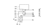
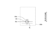
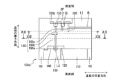
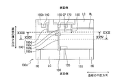
- FIG. 2 is a cross-sectional view illustrating a configuration of the solid-state imaging device according to the first embodiment.
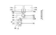
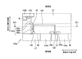
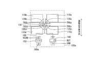
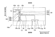
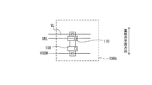
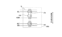
- FIG. 2 is a sectional view taken along line II-II of FIG. 1. It is a sectional view showing the composition of the solid-state image sensing device concerning a 2nd embodiment. It is a sectional view showing the composition of the solid-state image sensing device concerning a 3rd embodiment.
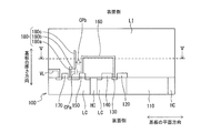
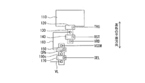
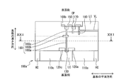
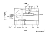
- FIG. 5 is a sectional view taken along line VV of FIG. 4. It is a sectional view showing the composition of the solid-state image sensing device concerning a 4th embodiment.
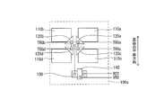
- FIG. 7 is a sectional view taken along line VII-VII of FIG. 6.
- FIG. 7 is a sectional view taken along line VIII-VIII of FIG. 6.
- FIG. 11 is a sectional view taken along line XI-XI in FIG. 10. It is a sectional view showing the composition of the solid-state image sensing device concerning a 5th embodiment. It is a sectional view showing the composition of the solid-state image sensing device concerning the modification of a 5th embodiment. It is a sectional view showing the composition of the solid-state image sensing device concerning a 6th embodiment.
- FIG. 14 is a cross-sectional view illustrating a configuration of a solid-state imaging device according to a modification of the sixth embodiment.
- FIG. 17 is a sectional view taken along line XII-XII of FIG. 16.
- FIG. 17 is a sectional view taken along line XIII-XIII of FIG. 16.
- FIG. 19 is a cross-sectional view illustrating a configuration of a solid-state imaging device according to a modification of the seventh embodiment.
- FIG. 21 is a sectional view taken along line XXI-XXI of FIG. 20. It is a sectional view showing the composition of the solid-state image sensing device concerning an 8th embodiment.
- FIG. 19 is a cross-sectional view illustrating a configuration of a solid-state imaging device according to a modification of the seventh embodiment.
- FIG. 21 is a sectional view taken along line XXI-XXI of FIG. 20. It is a sectional view showing the composition of the solid-state image sensing device concerning an 8th embodiment.
- FIG. 19 is a cross-sectional view illustrating a configuration of a solid-state imaging device according to a
- FIG. 23 is a sectional view taken along line XXIII-XXIII in FIG. 22.
- FIG. 23 is a sectional view taken along line XXIV-XXIV of FIG. 22.
- It is sectional drawing which shows the modification of 8th Embodiment.
- It is a sectional view showing the composition of the solid-state image sensing device concerning the modification of an 8th embodiment.
- FIG. 27 is a sectional view taken along line XXVII-XXVII of FIG. 26. It is a sectional view showing the composition of the solid-state image sensing device concerning a 9th embodiment.
- FIG. 2 is a cross-sectional view illustrating an example of an imaging device as a first application example of the present technology.
- FIG. 11 is a cross-sectional view illustrating an example of an electronic device as a second application example of the present technology.
- the solid-state imaging device according to the first embodiment constitutes one pixel (unit pixel) included in a solid-state imaging device used for a monitoring camera or the like such as a CCD image sensor or a CMOS image sensor.
- the first embodiment exemplifies a case where the solid-state imaging device forms a pixel of a so-called back-illuminated solid-state imaging device.
- the light receiving surface (the lower surface of the semiconductor substrate 100) of the semiconductor substrate 100 provided in the solid-state imaging device is referred to as “back surface”, and the surface ( The upper surface of the semiconductor substrate 100) may be referred to as “front surface”.
- the solid-state imaging device includes a photodiode 110, a transfer transistor 120, a floating diffusion 130, a reset transistor 140, and an amplification transistor 150.
- the solid-state imaging device includes a first wiring 160, a selection transistor 170, a vertical signal line VL, and a second wiring 180. 2, illustration of the high concentration region HC and the insulating layer LI shown in FIG. 1 is omitted.
- the high concentration region HC is a region having a larger doping amount than other regions (low concentration region LC) forming the solid-state imaging device.
- the insulating layer LI is formed of, for example, a silicon oxide film or the like.
- the photodiode 110 photoelectrically converts incident light, and generates and accumulates charges corresponding to the amount of photoelectric conversion.
- One end (anode electrode) of the photodiode 110 (photoelectric conversion element) is grounded.
- the other end (cathode electrode) of the photodiode 110 is connected to the source electrode of the transfer transistor 120.
- the transfer transistor 120 is disposed between the photodiode 110 and the floating diffusion 130.
- the drain electrode of the transfer transistor 120 is connected to the drain electrode of the reset transistor 140 and the gate electrode of the amplification transistor 150. Further, the transfer transistor 120 turns on or off the transfer of charges from the photodiode 110 to the floating diffusion 130 according to a drive signal TGR supplied to the gate electrode from a timing control unit (not shown). For example, when an H (High) level driving signal TGR is supplied to the gate electrode, the photoelectric conversion is performed by the photodiode 110 and the signal charges (for example, electrons) stored in the photodiode 110 are transferred to the floating diffusion 130. I do.
- the transfer of the signal charge to the floating diffusion 130 is stopped. Note that while the transfer transistor 120 stops transferring the signal charge to the floating diffusion 130, the charge photoelectrically converted by the photodiode 110 is accumulated in the photodiode 110.
- “High level” is described as “H level”
- “Low level” is described as “L level”.
- the H-level drive signal TGR and the L-level drive signal TGR are not distinguished from each other, and are denoted by a symbol “TGR”.
- the floating diffusion 130 is formed at a point (connection point) connecting the drain electrode of the transfer transistor 120, the source electrode of the reset transistor 140, and the gate electrode of the amplification transistor 150.
- the floating diffusion 130 accumulates charges transferred from the photodiode 110 via the transfer transistor 120 and converts the charges into a voltage. That is, the floating diffusion 130 transfers the signal charges accumulated in the photodiode 110.
- a configuration in which signal charges accumulated in one photodiode 110 are transferred to one floating diffusion 130 will be described.
- the reset transistor 140 has a source electrode connected to the floating diffusion 130 and a drain electrode connected to a pixel power supply (not shown). Further, the reset transistor 140 turns on or off discharge of the electric charge accumulated in the floating diffusion 130 according to the drive signal RST supplied to the gate electrode from the timing control unit. For example, when the H-level drive signal RST is supplied to the gate electrode, the reset transistor 140 causes the charge to flow to the pixel power supply before transferring the signal charge from the photodiode 110 to the floating diffusion 130. This discharges (resets) the charges accumulated in the floating diffusion 130. The amount of the discharged electric charge is an amount corresponding to the drain voltage VRD.
- the drain voltage VRD is a reset voltage for resetting the floating diffusion 130.
- the reset transistor 140 brings the floating diffusion 130 into an electrically floating state.
- the drive signal RST at the H level and the drive signal RST at the L level are indicated by reference numerals “RST” without distinction.
- the amplification transistor 150 is a source-grounded transistor in which a gate electrode is connected to the floating diffusion 130 and a source electrode is grounded. A control voltage VCOM is input to a source electrode of the amplification transistor 150 from a circuit (not shown). The drain electrode of the amplification transistor 150 is connected to the source electrode of the selection transistor 170. Further, the amplification transistor 150 reads the potential of the floating diffusion 130 reset by the reset transistor 140 as a reset level. Further, the amplification transistor 150 amplifies a voltage corresponding to the signal charge stored in the floating diffusion 130 to which the signal charge has been transferred by the transfer transistor 120. That is, the amplification transistor 150 reads out the signal charge transferred to the floating diffusion 130 as an electric signal and amplifies it. The voltage (voltage signal) amplified by the amplification transistor 150 is output to the vertical signal line VL via the selection transistor 170.
- the first wiring 160 is a wiring that connects the floating diffusion 130 and the gate electrode of the amplification transistor 150.
- the first wiring 160 is formed by a contact via forming step such that the length along the thickness direction (the vertical direction in FIG. 1) of the semiconductor substrate 100 is on the order of submicron to several microns. I do.
- the thickness direction of the semiconductor substrate 100 is referred to as “the thickness direction of the substrate”. The same applies to the following drawings.
- the selection transistor 170 has, for example, a drain electrode connected to one end of the vertical signal line VL, and a source electrode connected to the drain electrode of the amplification transistor 150. Further, the selection transistor 170 turns on or off the output of the voltage signal from the amplification transistor 150 to the vertical signal line VL according to the drive signal SEL supplied to the gate electrode from the timing control unit. For example, when the H-level drive signal SEL is supplied to the gate electrode, the selection transistor 170 outputs a voltage signal to the vertical signal line VL. On the other hand, when the L-level drive signal SEL is supplied to the gate electrode, the output of the voltage signal is stopped.
- the drive signal SEL at the H level and the drive signal SEL at the L level are indicated by reference numerals “SEL” without distinction.
- the selection transistor 170 is turned on when a selection control signal is applied to the gate electrode, and selects a unit pixel in synchronization with vertical scanning by a vertical scanning circuit (not shown). Note that the selection transistor 170 may be configured to be connected between the source electrode and the source line of the amplification transistor 150.
- the vertical signal line VL (vertical signal line) is a wiring for outputting an electric signal amplified by the amplification transistor 150.
- the drain electrode of the selection transistor 170 is connected to one end of the vertical signal line VL.
- An A / D converter (not shown) is connected to the other end of the vertical signal line VL.
- the second wiring 180 is electrically disposed downstream of the amplifying transistor 150, and has one end connected to the middle of the vertical signal line VL or to a node of the vertical signal line VL.
- the first wiring 160 the second wiring 180 is formed by a contact via forming step such that the length along the thickness direction of the semiconductor substrate 100 is on the order of submicron to several microns.
- the second wiring 180 faces at least a part of the first wiring 160. That is, at least a part of the first wiring 160 and at least a part of the second wiring 180 face each other.
- the additional capacitance CP is formed in a portion where the first wiring 160 and the second wiring 180 face each other.
- the magnitude of the additional capacitance CP depends on the distance between the first wiring 160 and the second wiring 180, the facing area of the portion where the first wiring 160 and the second wiring 180 face each other, and the like.
- the position of the additional capacitance CP is shown at a position different from the configuration in FIG.
- at least portions of the first wiring 160 and the second wiring 180 that face each other are parallel in the thickness direction of the semiconductor substrate 100. The configuration extending to the above will be described.
- first wiring 160 facing the second wiring 180 and a portion of the second wiring 180 facing the first wiring 160 are formed in the same process in order to suppress the occurrence of alignment variation due to the lithography process. Is desirable.
- the second wiring 180 is formed after forming the vertical signal line VL. For this reason, the second wiring 180 can be formed thicker than the vertical signal line VL.
- the opposing portion length OL which is the length of the portion of the first wiring 160 and the second wiring 180 facing each other, is different from that of the first wiring 160 and the second wiring 180.
- a configuration that is longer than the wiring interval WI which is the interval between the portions that are present, will be described.
- FIG. 1 shows a configuration in which the opposing portion length OL is shorter than the wiring interval WI for the sake of explanation, but in an actual configuration, the opposing portion length OL is longer than the wiring interval WI. It is.
- a photodiode 110, a transfer transistor 120, a floating diffusion 130, and a reset transistor 140 are formed on the semiconductor substrate 100. Further, on the semiconductor substrate 100, an amplification transistor 150, a first wiring 160, a selection transistor 170, a vertical signal line VL, and a second wiring 180 are formed.
- the conversion efficiency is adjusted while dispersing the main variation factor of the feedback capacitance. Becomes possible. This makes it possible to provide a solid-state imaging device capable of reducing the variation in conversion efficiency.
- first wiring 160 and the second wiring 180 facing each other extend in parallel along the thickness direction of the semiconductor substrate 100, there is no need to extend the wiring in the horizontal direction in the pixel, and the cell It is easy to combine with a small-sized pixel. Further, since it is not necessary to extend the wiring to the side of the adjacent pixel, electrical color mixing can be suppressed. Further, it is possible to minimize the addition of wiring extending in the width direction of the semiconductor substrate 100. This makes it possible to improve the degree of freedom in pixel layout.
- the additional capacitance CP can be increased as compared with the case where the opposing portion length OL is equal to or less than the wiring interval WI.
- the solid-state imaging device according to the second embodiment also has the cross-sectional structure illustrated in FIG. 1 and is common to the structure of the solid-state imaging device according to the first embodiment.
- the solid-state imaging device according to the second embodiment differs from the first embodiment in the configuration including two photodiodes 110a and 110b, as shown in FIG. In the following description, description of parts common to the first embodiment will be omitted.
- Each of the photodiodes 110a and 110b photoelectrically converts incident light, and generates and accumulates charges corresponding to the amount of photoelectric conversion.
- One end of the photodiode 110a is grounded, and the other end of the photodiode 110a is connected to a source electrode of the transfer transistor 120a.
- One end of the photodiode 110b is grounded, and the other end of the photodiode 110b is connected to the source electrode of the transfer transistor 120b.
- the transfer transistor 120a is arranged between the photodiode 110a and the floating diffusion 130. Further, the transfer transistor 120a turns on or off the transfer of charges from the photodiode 110a to the floating diffusion 130 according to the drive signal TGRa.
- the transfer transistor 120b is arranged between the photodiode 110b and the floating diffusion 130. Further, the transfer transistor 120b turns on or off the transfer of charges from the photodiode 110b to the floating diffusion 130 according to the drive signal TGRb.
- the signal charges stored in the plurality of photodiodes 110 are individually transferred to one floating diffusion 130. That is, in the second embodiment, a plurality of photodiodes 110 (photodiodes 110a and 110b) share one floating diffusion 130.
- the degree of freedom of the pixel layout can be improved without changing the size of the solid-state imaging device.
- the solid-state imaging device has a configuration in which the second wiring 180 is formed between the amplification transistor 150 and the selection transistor 170, as shown in FIGS. Different. In the following description, description of parts common to the first embodiment will be omitted.
- the second wiring 180 is formed by providing a via between the amplification transistor 150 and the selection transistor 170, for example.
- the second wiring 180 of the third embodiment includes a second wiring upstream part 180a, a second wiring middle part 180b, and a second wiring downstream part 180c.
- the second wiring upstream portion 180a forms an upstream side of the second wiring 180 on the semiconductor substrate 100.
- the second wiring upstream portion 180a is formed in a straight line along the thickness direction of the semiconductor substrate 100 (the vertical direction in FIG. 4).
- One end of the second wiring upstream portion 180a is connected to the source electrode of the selection transistor 170.
- the other end of the second wiring upstream portion 180a is connected to one end of the second wiring intermediate portion 180b.
- the first additional capacitance CPa is formed in a portion where the first wiring 160 and the second wiring upstream portion 180a face each other.
- the size of the first additional capacitance CPa depends on the distance between the first wiring 160 and the second wiring upstream portion 180a, the facing area of the portion where the first wiring 160 faces the second wiring upstream portion 180a, and the like. Value.
- the second wiring intermediate portion 180b is formed between the second wiring upstream portion 180a and the second wiring downstream portion 180c. Further, the second wiring intermediate portion 180b is formed in a linear shape extending along the plane direction of the semiconductor substrate 100.
- the second wiring downstream portion 180c forms a downstream side of the second wiring 180 on the semiconductor substrate 100.
- the second wiring downstream portion 180c is formed in a straight line along the thickness direction of the semiconductor substrate 100.
- One end of the second wiring downstream part 180c is connected to the other end of the second wiring intermediate part 180b.
- a part of the second wiring downstream part 180c faces a part of the first wiring 160 in the plane direction of the semiconductor substrate 100. That is, at least a part of the first wiring 160, at least a part of the second wiring upstream part 180a, and at least a part of the second wiring downstream part 180c face each other along the plane direction of the semiconductor substrate 100.
- the second additional capacitance CPb is formed in a portion where the first wiring 160 and the second wiring downstream portion 180c face each other.
- the size of the second additional capacitance CPb depends on the distance between the first wiring 160 and the second wiring downstream portion 180c, the facing area of the portion where the first wiring 160 faces the second wiring downstream portion 180c, and the like. Value.
- the distance between the second wiring downstream part 180c and the first wiring 160 is smaller than the distance between the second wiring upstream part 180a and the first wiring 160. That is, the distance between at least a part of the first wiring 160 and the at least one part of the second wiring upstream part 180a facing each other, and at least one of the at least one part of the first wiring 160 and the second wiring downstream part 180c facing each other.
- the interval with the part is different.
- the conversion efficiency can be adjusted while dispersing the main variation factors of the feedback capacitance. For this reason, it is possible to provide a solid-state imaging device capable of reducing variation in conversion efficiency. This is because in the solid-state imaging device in which the amplification transistor 150 is connected to the source ground as in the present technology, the capacitance formed between the amplification transistor 150 and the selection transistor 170 is also included as the feedback capacitance.
- the degree of freedom for the configuration of the second wiring 180 is improved. It can be improved.
- the configuration of the second wiring 180 is configured to include the second wiring upstream portion 180a, the second wiring intermediate portion 180b, and the second wiring downstream portion 180c, but is not limited thereto. is not. That is, for example, the second wiring 180 may be formed only of a portion having one end connected to the source electrode of the selection transistor 170 and formed linearly along the thickness direction of the semiconductor substrate 100.
- the solid-state imaging device according to the fourth embodiment includes two stacked semiconductor substrates (a first semiconductor substrate 100a and a second semiconductor substrate 100b) (two-layer structure). Further, in the solid-state imaging device according to the fourth embodiment, the second wiring 180 includes a second wiring upstream part 180a, a second wiring intermediate part 180b, and a second wiring downstream part 180c. Note that, in the drawing, the insulating layer LI of the first semiconductor substrate 100a and the insulating layer LI of the second semiconductor substrate 100b are indicated by one symbol “LI”. This is the same in the following drawings.
- the photodiode 110 On the first semiconductor substrate 100a, the photodiode 110, the transfer transistor 120, the floating diffusion 130, and the reset transistor 140 are formed. Further, a part of the amplification transistor 150, the first wiring 160, the second wiring upstream part 180a, and the second wiring intermediate part 180b are formed on the first semiconductor substrate 100a. On the second semiconductor substrate 100b, a part of the second wiring middle part 180b, the second wiring downstream part 180c, the selection transistor 170, and the vertical signal line VL are formed.
- the photodiode 110, the floating diffusion 130, and the amplification transistor 150 are formed on one semiconductor substrate (first semiconductor substrate 100a) among the plurality of semiconductor substrates.
- the first wiring 160 and a part of the second wiring 180 are formed on the first semiconductor substrate 100a.
- Another part of the second wiring 180 is formed on another semiconductor substrate (the second semiconductor substrate 100b) among the plurality of semiconductor substrates. Is formed.
- the second wiring upstream portion 180a is formed on one semiconductor substrate 100 (first semiconductor substrate 100a).
- the second wiring upstream portion 180a is formed in a straight line along the thickness direction of the semiconductor substrate 100 (the vertical direction in FIG. 6).
- One end of the second wiring upstream portion 180a is connected to the drain electrode of the amplification transistor 150.
- the second wiring upstream portion 180a faces a part of the first wiring 160 in the plane direction of the semiconductor substrate 100 (the horizontal direction in FIG. 6).
- the additional capacitance CP is formed in a portion where the first wiring 160 and the second wiring upstream portion 180a face each other.
- the magnitude of the additional capacitance CP depends on the distance between the first wiring 160 and the second wiring upstream part 180a, the facing area of the part where the first wiring 160 and the second wiring upstream part 180a face each other, and the like.
- the second wiring intermediate part 180b is formed between the second wiring upstream part 180a and the second wiring downstream part 180c. Further, the second wiring intermediate portion 180b is formed in a linear shape extending along the plane direction of the semiconductor substrate 100. Part of the second wiring intermediate portion 180b is formed on a surface of the first semiconductor substrate 100a facing the second semiconductor substrate 100b. Further, the other end of the second wiring upstream portion 180a is connected to a part of the second wiring intermediate portion 180b. The other part of the second wiring intermediate part 180b is formed on the surface of the second semiconductor substrate 100b facing the first semiconductor substrate 100a. In addition, one end of the second wiring downstream part 180c is connected to another part of the second wiring intermediate part 180b.
- the second wiring downstream portion 180c is formed on another semiconductor substrate 100 (second semiconductor substrate 100b). Further, the second wiring downstream portion 180c is formed in a straight line along the thickness direction of the semiconductor substrate 100 (the vertical direction in FIG. 6). The other end of the second wiring downstream portion 180c is connected to the source electrode of the selection transistor 170.
- the number of components arranged on each of the first semiconductor substrate 100a and the second semiconductor substrate 100b is smaller than the configuration in which all the components are formed on one semiconductor substrate. Can be reduced. For this reason, it is possible to improve the degree of freedom in layout as compared with a configuration in which all the components are formed on one semiconductor substrate.
- the configuration of the second wiring 180 includes the second wiring upstream portion 180a, the second wiring intermediate portion 180b, and the second wiring downstream portion 180c, but is not limited thereto. . That is, for example, the second wiring 180 may be configured to include the second wiring upstream portion 180a and the second wiring downstream portion 180c.
- the solid-state imaging device includes two stacked semiconductor substrates 100 (the first semiconductor substrate 100a and the second semiconductor substrate 100b). However, the present invention is not limited to this. That is, for example, a configuration in which a support substrate is stacked on the surface of the first semiconductor substrate 100a opposite to the surface facing the second semiconductor substrate 100b, and the solid-state imaging device is provided with three or more semiconductor substrates stacked. Good.
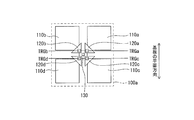
- a configuration may be adopted in which signal charges accumulated in the two photodiodes 110a and 110b are individually transferred to one floating diffusion 130. Further, for example, as shown in FIGS. 10 and 11, the signal charges accumulated in the four photodiodes 110a to 110d may be individually transferred to one floating diffusion 130.
- the solid-state imaging device includes two stacked semiconductor substrates (a first semiconductor substrate 100a and a second semiconductor substrate 100b).
- the second wiring 180 includes a second wiring upstream part 180a, a second wiring intermediate part 180b, and a second wiring downstream part 180c.
- the photodiode 110 On the first semiconductor substrate 100a, the photodiode 110, the transfer transistor 120, the floating diffusion 130, and the reset transistor 140 are formed. Further, a part of the amplification transistor 150, the first wiring 160, the second wiring upstream part 180a, and the second wiring intermediate part 180b are formed on the first semiconductor substrate 100a. On the second semiconductor substrate 100b, a part of the second wiring middle part 180b, the second wiring downstream part 180c, the selection transistor 170, and the vertical signal line VL are formed.
- the second wiring upstream portion 180a is formed on the first semiconductor substrate 100a.
- the first semiconductor substrate 100a is formed in a straight line along the thickness direction (vertical direction in FIG. 12).
- One end of the second wiring upstream portion 180a is connected to the drain electrode of the amplification transistor 150.
- a part of the second wiring upstream part 180a is opposed to a part of the first wiring 160 in the plane direction (the left-right direction in FIG. 12) of the semi-first semiconductor substrate 100a.
- the first additional capacitance CPa is formed in a portion where the first wiring 160 and the second wiring upstream portion 180a face each other.
- the size of the first additional capacitance CPa depends on the distance between the first wiring 160 and the second wiring upstream portion 180a, the facing area of the portion where the first wiring 160 faces the second wiring upstream portion 180a, and the like. Value.
- the second wiring intermediate part 180b is formed between the second wiring upstream part 180a and the second wiring downstream part 180c. Further, the second wiring intermediate portion 180b is formed in a linear shape extending along the plane direction of the two semiconductor substrates (the first semiconductor substrate 100a and the second semiconductor substrate 100b) that are stacked. Part of the second wiring intermediate portion 180b is formed on a surface of the first semiconductor substrate 100a facing the second semiconductor substrate 100b. Further, the other end of the second wiring upstream portion 180a is connected to a part of the second wiring intermediate portion 180b.
- the other part of the second wiring intermediate part 180b is formed on the surface of the second semiconductor substrate 100b facing the first semiconductor substrate 100a.
- one end of the second wiring downstream part 180c is connected to another part of the second wiring intermediate part 180b.
- the length of the second wiring intermediate portion 180b is opposite to the second wiring intermediate portion 180b along the direction in which the first wiring 160 and the plurality of semiconductor substrates (the first semiconductor substrate 100a and the second semiconductor substrate 100b) are stacked. Set to the length where the part is formed. That is, at least a part of the first wiring 160 and at least a part of the second wiring intermediate part 180b face each other along the direction in which the plurality of semiconductor substrates are stacked.
- the second additional capacitance CPb is formed in a part where a part of the first wiring 160 and a part of the second wiring intermediate part 180b face each other.
- the size of the second additional capacitance CPb depends on the distance between the first wiring 160 and the second wiring intermediate part 180b, the facing area of the part where the first wiring 160 and the second wiring intermediate part 180b face each other, and the like. Value.
- the second wiring downstream portion 180c is formed on the second semiconductor substrate 100b.
- the second wiring downstream portion 180c is formed in a straight line along the thickness direction of the second semiconductor substrate 100b.
- the other end of the second wiring downstream portion 180c is connected to the source electrode of the selection transistor 170.
- the configuration of the fifth embodiment it is possible to increase the feedback capacitance as compared with the configuration in which the additional capacitance is formed only in the portion where the first wiring 160 and the second wiring upstream portion 180a face each other. Becomes
- a configuration in which only one photodiode 110 is connected to one floating diffusion 130 is not limited to this. That is, for example, as shown in FIG. 13, the signal charges accumulated in the two photodiodes 110 a and 110 b may be individually transferred to one floating diffusion 130.
- the solid-state imaging device includes two stacked semiconductor substrates 100 (a first semiconductor substrate 100a and a second semiconductor substrate 100b).
- the second wiring 180 includes a second wiring upstream part 180a, a second wiring intermediate part 180b, and a second wiring downstream part 180c.
- the solid-state imaging device according to the sixth embodiment includes a third wiring upstream portion 190a, a third wiring intermediate portion 190b, and a third wiring downstream portion 190c, and is connected to the first wiring 160 to be connected to the first wiring 160.
- the photodiode 110 On the first semiconductor substrate 100a, the photodiode 110, the transfer transistor 120, the floating diffusion 130, and the reset transistor 140 are formed. Further, on the first semiconductor substrate 100a, the amplification transistor 150, the first wiring 160, the second wiring upstream portion 180a, a part of the second wiring intermediate portion 180b, the third wiring upstream portion 190a, and the third wiring intermediate portion 190b Is formed. On the second semiconductor substrate 100b, a part of the second wiring intermediate part 180b, a part of the second wiring downstream part 180c, a part of the third wiring intermediate part 190b, a part of the third wiring downstream part 190c, the selection transistor 170, the vertical signal line VL is formed.
- the second wiring upstream portion 180a is formed in a straight line along the thickness direction (the vertical direction in FIG. 14) of the first semiconductor substrate 100a. One end of the second wiring upstream portion 180a is connected to the drain electrode of the amplification transistor 150.
- the first additional capacitance CPa is formed in a portion where a part of the first wiring 160 and a part of the second wiring upstream part 180a face each other.
- the size of the first additional capacitance CPa depends on the distance between the first wiring 160 and the second wiring upstream portion 180a, the facing area of the portion where the first wiring 160 faces the second wiring upstream portion 180a, and the like. Value.
- the second wiring intermediate part 180b is formed between the second wiring upstream part 180a and the second wiring downstream part 180c. Further, the second wiring intermediate portion 180b is formed in a linear shape extending along the plane direction of the first semiconductor substrate 100a. Part of the second wiring intermediate portion 180b is formed on a surface of the first semiconductor substrate 100a facing the second semiconductor substrate 100b. Further, the other end of the second wiring upstream portion 180a is connected to a part of the second wiring intermediate portion 180b. The other part of the second wiring intermediate part 180b is formed on the surface of the second semiconductor substrate 100b facing the first semiconductor substrate 100a. In addition, one end of the second wiring downstream part 180c is connected to another part of the second wiring intermediate part 180b.
- the second wiring downstream portion 180c is formed linearly along the thickness direction of the second semiconductor substrate 100b. The other end of the second wiring downstream portion 180c is connected to the source electrode of the selection transistor 170.
- the third wiring upstream portion 190a is formed on the first semiconductor substrate 100a.
- the first semiconductor substrate 100a is formed in a straight line along the thickness direction.
- One end of the third wiring upstream portion 190a is connected to a linear portion of the first wiring 160 connected to the gate electrode of the amplification transistor 150 along the thickness direction of the first semiconductor substrate 100a.
- the third wiring intermediate portion 190b is formed between the third wiring upstream portion 190a and the third wiring downstream portion 190c.
- the third wiring intermediate portion 190b is formed in a straight line extending along the plane direction of the two semiconductor substrates (the first semiconductor substrate 100a and the second semiconductor substrate 100b) that are stacked. Part of the third wiring intermediate portion 190b is formed on a surface of the first semiconductor substrate 100a facing the second semiconductor substrate 100b. The other end of the third wiring upstream portion 190a is connected to a part of the third wiring intermediate portion 190b.
- Another portion of the third wiring intermediate portion 190b is provided on a surface of the second semiconductor substrate 100b facing the first semiconductor substrate 100a.
- one end of the third wiring downstream part 190c is connected to the other part of the third wiring intermediate part 190b.
- the third wiring downstream portion 190c is formed in a straight line along the thickness direction of the second semiconductor substrate 100b.
- the third wiring downstream portion 190c is opposed to a part of the second wiring downstream portion 180c in the plane direction (the horizontal direction in FIG. 14) of the semiconductor substrate (the second semiconductor substrate 100b). That is, at least a part of the second wiring 180 and at least a part of the third wiring 190 face each other.
- the second additional capacitance CPb is formed in a portion where the third wiring downstream portion 190c and the second wiring downstream portion 180c face each other.
- the size of the second additional capacitance CPb is determined by the distance between the third wiring downstream portion 190c and the second wiring downstream portion 180c or the distance between the third wiring downstream portion 190c and the second wiring downstream portion 180c. The value depends on the area and the like. At least portions of the second wiring 180 and the third wiring 190 facing each other extend in parallel along the thickness direction of the semiconductor substrate (the second semiconductor substrate 100b).
- the feedback capacitance As compared with a configuration in which the additional capacitance is formed only in a portion where the first wiring 160 and the second wiring upstream portion 180a face each other. Becomes
- the configuration of the second wiring 180 includes the second wiring upstream portion 180a, the second wiring intermediate portion 180b, and the second wiring downstream portion 180c, but is not limited thereto. . That is, for example, the second wiring 180 may be configured to include the second wiring upstream portion 180a and the second wiring downstream portion 180c. Similarly, the third wiring 190 may be configured to include a third wiring upstream portion 190a and a third wiring downstream portion 190c. Further, for example, as shown in FIG. 15, the signal charges accumulated in the two photodiodes 110a and 110b may be individually transferred to one floating diffusion 130.
- the solid-state imaging device includes two stacked semiconductor substrates 100 (a first semiconductor substrate 100a and a second semiconductor substrate 100b), as shown in FIGS.
- the first wiring 160 includes a first wiring upstream part 160a, a first wiring intermediate part 160b, and a first wiring downstream part 160c.
- the amplification transistor 150 On the first semiconductor substrate 100a, a part of the photodiode 110, the transfer transistor 120, the floating diffusion 130, the reset transistor 140, the first wiring upstream part 160a, and the first wiring intermediate part 160b are formed.
- the amplification transistor 150 On the second semiconductor substrate 100b, the amplification transistor 150, a part of the first wiring intermediate part 160b, the first wiring downstream part 160c, the selection transistor 170, the vertical signal line VL, and the second wiring 180 are formed.
- the photodiode 110, the floating diffusion 130, and the first wiring upstream portion 160a are formed on one semiconductor substrate (first semiconductor substrate 100a). Further, on another semiconductor substrate (second semiconductor substrate 100b), the amplification transistor 150, the first wiring downstream part 160c, the vertical signal line VL, and the second wiring 180 are formed.
- the first wiring 160 includes a first wiring upstream portion 160a formed on one semiconductor substrate (first semiconductor substrate 100a) and a first wiring upstream portion 160a formed on another semiconductor substrate (second semiconductor substrate 100b). Includes a wiring downstream section 160c. Further, the first wiring 160 includes a first wiring intermediate part 160b formed between the first wiring upstream part 160a and the first wiring downstream part 160c.
- the first wiring upstream portion 160a forms the upstream side of the first wiring 160 on the first semiconductor substrate 100a, and is formed in a straight line along the thickness direction (the vertical direction in FIG. 16) of the first semiconductor substrate 100a. Is formed. One end of the first wiring upstream portion 160a is connected to the gate electrode of the transfer transistor 120.
- the first wiring intermediate portion 160b is formed in a linear shape extending along the plane direction of the two semiconductor substrates (the first semiconductor substrate 100a and the second semiconductor substrate 100b) that are stacked. A part of the first wiring intermediate part 160b is provided on a surface of the first semiconductor substrate 100a facing the second semiconductor substrate 100b. Further, the other end of the first wiring upstream portion 160a is connected to a part of the first wiring intermediate portion 160b. The other part of the first wiring intermediate part 160b is provided on a surface of the second semiconductor substrate 100b facing the first semiconductor substrate 100a. Further, one end of the first wiring downstream portion 160c is connected to another portion of the first wiring intermediate portion 160b.
- the first wiring downstream portion 160c forms a downstream side of the first wiring 160 on the second semiconductor substrate 100b, and is formed in a straight line along the thickness direction of the second semiconductor substrate 100b.
- the other end of the first wiring downstream portion 160c is connected to the gate electrode of the amplification transistor 150.
- first wiring downstream part 160c faces the second wiring 180, one end of which is connected in the middle of the vertical signal line VL, in the plane direction of the second semiconductor substrate 100b (the horizontal direction in FIG. 16).
- the additional capacitance CP is formed in a portion where the first wiring downstream portion 160c and the second wiring 180 face each other.
- the magnitude of the additional capacitance CP depends on the distance between the first wiring downstream portion 160c and the second wiring 180, the facing area of the portion where the first wiring downstream portion 160c faces the second wiring 180, and the like.
- at least portions of the first wiring downstream portion 160c and the second wiring 180 facing each other extend in parallel along the thickness direction of another semiconductor substrate (second semiconductor substrate 100b).
- the seventh embodiment compared to a configuration in which components upstream (upstream) of the amplification transistor 150 are formed on the first semiconductor substrate 100a, components arranged on the first semiconductor substrate 100a Can be reduced. For this reason, it is possible to improve the layout flexibility.
- the configuration of the first wiring 160 includes the first wiring upstream portion 160a, the first wiring intermediate portion 160b, and the first wiring downstream portion 160c, but is not limited thereto. . That is, for example, the first wiring 160 may be configured to include the first wiring upstream portion 160a and the first wiring downstream portion 160c.
- the signal charges accumulated in the two photodiodes 110a and 110b may be individually transferred to one floating diffusion 130.
- the signal charges stored in the four photodiodes 110a to 110d may be individually transferred to one floating diffusion 130.
- the solid-state imaging device according to the eighth embodiment includes two stacked semiconductor substrates 100 (a first semiconductor substrate 100a and a second semiconductor substrate 100b).
- the first wiring 160 includes a first wiring upstream portion 160a, a first wiring intermediate portion 160b, a first wiring downstream portion 160c, and a first wiring branching portion 160d. Including.
- the photodiode 110 On the first semiconductor substrate 100a, the photodiode 110, the transfer transistor 120, the floating diffusion 130, a part of the first wiring upstream part 160a, and a part of the first wiring intermediate part 160b are formed.
- the reset transistor 140, the amplification transistor 150, a part of the first wiring middle part 160b, the first wiring downstream part 160c, the first wiring branch part 160d, the selection transistor 170, the vertical signal line VL, The second wiring 180 is formed.
- the first wiring upstream portion 160a forms the upstream side of the first wiring 160 on the first semiconductor substrate 100a, and is formed in a straight line along the thickness direction (the vertical direction in FIG. 22) of the first semiconductor substrate 100a. Is formed. One end of the first wiring upstream portion 160a is connected to the gate electrode of the transfer transistor 120.
- the first wiring intermediate portion 160b is formed in a linear shape extending along the plane direction of the two semiconductor substrates (the first semiconductor substrate 100a and the second semiconductor substrate 100b) that are stacked. A part of the first wiring intermediate part 160b is provided on a surface of the first semiconductor substrate 100a facing the second semiconductor substrate 100b. Further, the other end of the first wiring upstream portion 160a is connected to a part of the first wiring intermediate portion 160b. The other part of the first wiring intermediate part 160b is provided on a surface of the second semiconductor substrate 100b facing the first semiconductor substrate 100a. Further, one end of the first wiring downstream portion 160c is connected to another portion of the first wiring intermediate portion 160b.
- the first wiring downstream portion 160c forms a downstream side of the first wiring 160 on the second semiconductor substrate 100b, and is formed in a straight line along the thickness direction of the second semiconductor substrate 100b.
- the other end of the first wiring downstream portion 160c is connected to the gate electrode of the amplification transistor 150.
- the additional capacitance CP is formed in a portion where the first wiring downstream portion 160c and the second wiring 180 face each other.
- the magnitude of the additional capacitance CP depends on the distance between the first wiring downstream portion 160c and the second wiring 180, the facing area of the portion where the first wiring downstream portion 160c faces the second wiring 180, and the like.
- the first wiring branching portion 160d is formed by branching from between both end portions of the first wiring downstream portion 160c. One end of the first wiring branch part 160d is connected to the first wiring upstream part 160a. The other end of the first wiring branch part 160d is connected to the source electrode of the reset transistor 140.
- the components arranged on the first semiconductor substrate 100a are compared with the configuration in which components upstream (upstream) of the reset transistor 140 are formed on the first semiconductor substrate 100a. Can be reduced. For this reason, it is possible to improve the layout flexibility.
- the configuration of the first wiring 160 includes the first wiring upstream portion 160a, the first wiring intermediate portion 160b, and the first wiring downstream portion 160c, but is not limited to this. . That is, for example, the first wiring 160 may be configured to include the first wiring upstream portion 160a and the first wiring downstream portion 160c.
- a configuration may be adopted in which signal charges accumulated in the two photodiodes 110a and 110b are individually transferred to one floating diffusion 130. Further, for example, as shown in FIGS. 26 and 27, the signal charges accumulated in the four photodiodes 110a to 110d may be individually transferred to one floating diffusion 130.
- the solid-state imaging device includes two stacked semiconductor substrates 100 (a first semiconductor substrate 100a and a second semiconductor substrate 100b).
- the first wiring 160 includes a first wiring upstream part 160a, a first wiring intermediate part 160b, a first wiring downstream part 160c, and a first wiring branch part 160d. Including.
- the photodiode 110 On the first semiconductor substrate 100a, the photodiode 110, the transfer transistor 120, the floating diffusion 130, the reset transistor 140, a part of the first wiring upstream part 160a, and a part of the first wiring intermediate part 160b are formed.
- the amplification transistor 150 On the second semiconductor substrate 100b, the amplification transistor 150, a part of the first wiring intermediate part 160b, the first wiring downstream part 160c, the first wiring branch part 160d, the selection transistor 170, the vertical signal line VL, and the second wiring 180 Are formed.
- the first wiring upstream part 160a forms the upstream side of the first wiring 160 on the first semiconductor substrate 100a, and is formed in a straight line along the thickness direction (the vertical direction in FIG. 28) of the first semiconductor substrate 100a. Is formed. One end of the first wiring upstream portion 160a is connected to the gate electrode of the transfer transistor 120.
- the first wiring intermediate portion 160b is formed in a linear shape extending along the plane direction of the two semiconductor substrates (the first semiconductor substrate 100a and the second semiconductor substrate 100b) that are stacked. A part of the first wiring intermediate part 160b is provided on a surface of the first semiconductor substrate 100a facing the second semiconductor substrate 100b. Further, the other end of the first wiring upstream portion 160a is connected to a part of the first wiring intermediate portion 160b. The other part of the first wiring intermediate part 160b is provided on a surface of the second semiconductor substrate 100b facing the first semiconductor substrate 100a. Further, one end of the first wiring downstream portion 160c is connected to another portion of the first wiring intermediate portion 160b.
- the first wiring downstream portion 160c forms a downstream side of the first wiring 160 on the second semiconductor substrate 100b, and is formed in a straight line along the thickness direction of the second semiconductor substrate 100b.
- the other end of the first wiring downstream part 160c is connected to one end of the first wiring branch part 160d.
- the other end of the first wiring branch part 160d is connected to the gate electrode of the amplification transistor 150. Further, a part of the first wiring branch part 160d is opposed to the second wiring 180 in the plane direction of the semiconductor substrate 100 (the horizontal direction in FIG. 28).
- the additional capacitance CP is formed in a portion where the first wiring branch part 160d and the second wiring 180 face each other.
- the magnitude of the additional capacitance CP depends on the distance between the first wiring branch 160d and the second wiring 180, the facing area of the portion where the first wiring branch 160d faces the second wiring 180, and the like.
- the gate oxide films (not shown) of the amplification transistor 150 and the selection transistor 170 are set to be smaller than the surface of the second semiconductor substrate 100b. It is arranged at a position near one semiconductor substrate 100a. According to the configuration of the ninth embodiment, it is possible to improve the degree of freedom of the layout for arranging the elements constituting the solid-state imaging device.
- the solid-state imaging device according to the present technology can have, for example, a configuration illustrated in FIG. 29.
- the solid-state imaging device 1 shown in FIG. 29 is a CMOS image sensor. Further, the solid-state imaging device 1 has a pixel region 4 as an imaging area on the semiconductor substrate 100. Further, in the peripheral area of the pixel area 4, for example, a peripheral circuit section (5, 6, 7, 8, 9) including a vertical drive circuit 5, a column selection circuit 6, a horizontal drive circuit 7, an output circuit 8, and a control circuit 9 Having.
- the pixel region 4 has, for example, a plurality of unit pixels 3 (corresponding to the photodiode 110) two-dimensionally arranged in a matrix.
- a pixel drive line VD (specifically, a row selection line and a reset control line) is wired for each pixel row, and a vertical signal line VL is wired for each pixel column.
- the pixel drive line VD transmits a drive signal for reading a signal from a pixel.
- One end of the pixel drive line VD is connected to an output end corresponding to each row of the vertical drive circuit 5.
- the vertical drive circuit 5 includes a shift register, an address decoder, and the like.
- the vertical drive circuit 5 drives each unit pixel 3 of the pixel region 4 in, for example, a row unit.
- a signal output from each unit pixel 3 of the pixel row selectively scanned by the vertical drive circuit 5 is supplied to the column selection circuit 6 through each of the vertical signal lines VL.
- the column selection circuit 6 includes an amplifier, a horizontal selection switch, and the like provided for each vertical signal line VL.
- the horizontal drive circuit 7 includes a shift register, an address decoder, and the like.
- the horizontal drive circuit 7 sequentially drives the horizontal selection switches of the column selection circuit 6 while scanning them.
- the signal of each pixel transmitted through each of the vertical signal lines VL is sequentially output to the horizontal signal line VH and transmitted to the outside of the semiconductor substrate 100 through the horizontal signal line VH.
- the circuit portion including the vertical drive circuit 5, the column selection circuit 6, the horizontal drive circuit 7, and the horizontal signal line VH may be formed on the semiconductor substrate 100, or may be provided on an external control IC. You may. Further, those circuit portions may be formed on another substrate connected by a cable or the like.
- the control circuit 9 receives a clock supplied from outside the semiconductor substrate 100, data instructing an operation mode, and the like, and outputs data such as internal information of the solid-state imaging device 1. Further, the control circuit 9 has a timing generator that generates various timing signals, and controls the vertical drive circuit 5, the column selection circuit 6, the horizontal drive circuit 7, and the like based on the various timing signals generated by the timing generator. Controls driving of peripheral circuits.
- FIG. 30 shows a schematic configuration of an electronic device 2 (camera) as a second application example.
- the electronic device 2 is, for example, a video camera capable of capturing a still image or a moving image, and drives the solid-state imaging device 1, an optical system (optical lens) 201, a shutter device 202, and the solid-state imaging device 1 and the shutter device 202. And a signal processing unit 203.
- the optical system 201 guides image light (incident light) from a subject to the pixel region 4 of the solid-state imaging device 1.
- the optical system 201 may include a plurality of optical lenses.
- the shutter device 202 controls a light irradiation period and a light blocking period to the solid-state imaging device 1.
- the drive unit 204 controls the transfer operation of the solid-state imaging device 1 and the shutter operation of the shutter device 202.
- the signal processing unit 203 performs various kinds of signal processing on the signal output from the solid-state imaging device 1.
- the video signal after the signal processing is stored in a storage medium such as a memory or output to a monitor or the like.
- the configuration of the back-illuminated solid-state imaging device is illustrated, but the present disclosure is also applicable to a front-illuminated solid-state imaging device.
- the solid-state imaging device according to the present disclosure does not need to include all of the components described in the above-described embodiments and the like, and may include other components.
- the technology of the present disclosure can be applied not only to a solid-state imaging device but also to, for example, a solar cell.
- the technology of the present disclosure can be applied not only to surveillance cameras and the like, but also to mobile devices such as mobile phones and in-vehicle devices. It should be noted that the effects described in the present specification are merely examples, are not limited, and may have other effects.
- the present technology can have the following configurations.
- a floating diffusion in which signal charges accumulated in a photodiode performing photoelectric conversion are transferred;
- a source-grounded amplification transistor that reads and amplifies the signal charge transferred to the floating diffusion as an electric signal,
- a first wiring connecting the floating diffusion and the amplification transistor A second wiring electrically disposed downstream of the amplification transistor,
- a solid-state imaging device in which at least a part of the first wiring and at least a part of the second wiring face each other.
- the second wiring is formed between the upstream portion of the second wiring, the downstream portion of the second wiring, and the upstream portion of the second wiring and the downstream portion of the second wiring, and extends along a plane direction of the stacked semiconductor substrates.
- a second wiring intermediate portion extending The solid-state imaging device according to (4), wherein at least a part of the first wiring and at least a part of the intermediate part of the second wiring face each other along a direction in which the plurality of semiconductor substrates are stacked.
- a vertical signal line that outputs an electric signal amplified by the amplification transistor The solid-state imaging device according to any one of (1) to (7), wherein one end of the second wiring is connected to the middle of the vertical signal line or to a node of the vertical signal line.
- the first wiring is a first wiring upstream portion that forms the upstream side of the first wiring on one of the plurality of semiconductor substrates, and the first wiring on the other semiconductor substrate of the plurality of semiconductor substrates.
- the solid-state imaging device according to (1) wherein at least a part of the downstream portion of the first wiring and at least a part of the second wiring face each other.
- (11) Comprising a plurality of the photodiodes, The solid-state imaging device according to any one of (1) to (10), wherein the signal charges respectively accumulated in the plurality of photodiodes are individually transferred to one of the floating diffusions. (12) A third wiring branched from the first wiring, The solid-state imaging device according to any one of (1) to (11), wherein at least a part of the second wiring and at least a part of the third wiring are opposed to each other. (13) Comprising a semiconductor substrate on which the floating diffusion and the amplification transistor are formed, The solid-state imaging device according to (12), wherein at least portions of the second wiring and the third wiring facing each other extend in parallel along a thickness direction of the semiconductor substrate. (14) The solid-state imaging device according to any one of (1) to (13), wherein a length of the first wiring and the second wiring facing each other is longer than a distance between the mutually facing parts. .
- SYMBOLS 1 Solid-state imaging device, 2 ... Electronic equipment, 3 ... Unit pixel, 4 ... Pixel area, 5 ... Vertical drive circuit, 6 ... Column selection circuit, 7 ... Horizontal drive circuit, 8 ... Output circuit, 9 ... Control circuit, 100 ... semiconductor substrate, 100a ... first semiconductor substrate, 100b ... second semiconductor substrate, 110 ... photodiode, 120 ... transfer transistor, 130 ... floating diffusion, 140 ... reset transistor, 150 ... amplification transistor, 160 ... first wiring, 160a ... First wiring upstream part, 160b ... First wiring middle part, 160c ... First wiring downstream part, 160d ... First wiring branch part, 170 ... Selection transistor, 180 ... Second wiring, 180a ...
Landscapes
- Engineering & Computer Science (AREA)
- Multimedia (AREA)
- Signal Processing (AREA)
- Solid State Image Pick-Up Elements (AREA)
- Transforming Light Signals Into Electric Signals (AREA)
Abstract
Description
フローティングディフュージョンには、光電変換を行うフォトダイオードに蓄積された信号電荷が転送される。増幅トランジスタは、フローティングディフュージョンに転送された信号電荷を電気信号として読み出して増幅する。第一配線は、フローティングディフュージョンと増幅トランジスタとを接続する。第二配線は、増幅トランジスタよりも電気的に下流側へ配置されている。また、第一配線の少なくとも一部と第二配線の少なくとも一部とが対向している。
<固体撮像素子の全体構成>
第1実施形態に係る固体撮像素子は、例えば、CCDイメージセンサやCMOSイメージセンサ等、監視カメラ等に用いる固体撮像装置が備える1つの画素(単位画素)を構成する。
また、第1実施形態では、固体撮像素子が、いわゆる裏面照射型の固体撮像装置の画素を構成する場合を例示する。このため、以降の説明では、図1において、固体撮像素子が備える半導体基板100の受光面(半導体基板100の下面)を「裏面」と記載し、半導体基板100の裏面とは反対側の面(半導体基板100の上面)を「表面」と記載する場合がある。
高濃度領域HCは、固体撮像素子を形成するその他の領域(低濃度領域LC)よりもドーピング量が多い領域である。絶縁層LIは、例えば、シリコン酸化膜等で形成されている。
フォトダイオード110(光電変換素子)の一端(アノード電極)は、接地されている。フォトダイオード110の他端(カソード電極)は、転送トランジスタ120のソース電極に接続されている。
また、転送トランジスタ120は、図外のタイミング制御部からゲート電極に供給される駆動信号TGRに従って、フォトダイオード110からフローティングディフュージョン130への電荷の転送をオンまたはオフする。例えば、H(High)レベルの駆動信号TGRがゲート電極に供給されると、フォトダイオード110で光電変換されて、フォトダイオード110に蓄積された信号電荷(例えば、電子)を、フローティングディフュージョン130に転送する。一方、L(Low)レベルの駆動信号TGRがゲート電極に供給されると、フローティングディフュージョン130への信号電荷の転送を停止する。なお、転送トランジスタ120がフローティングディフュージョン130への信号電荷の転送を停止している間、フォトダイオード110が光電変換した電荷は、フォトダイオード110に蓄積される。なお、以降の説明では、「Highレベル」を「Hレベル」と記載し、「Lowレベル」を「Lレベル」と記載する。また、図中では、Hレベルの駆動信号TGRとLレベルの駆動信号TGRを区別せずに、符号「TGR」で示す。
また、フローティングディフュージョン130は、フォトダイオード110から転送トランジスタ120を介して転送されてくる電荷を蓄積し、電圧に変換する。すなわち、フローティングディフュージョン130は、フォトダイオード110に蓄積された信号電荷が転送される。
第1実施形態では、一つのフォトダイオード110に蓄積された信号電荷が、一つのフローティングディフュージョン130に転送される構成について説明する。
また、リセットトランジスタ140は、タイミング制御部からゲート電極に供給される駆動信号RSTに従って、フローティングディフュージョン130に蓄積されている電荷の排出をオンまたはオフする。例えば、リセットトランジスタ140は、Hレベルの駆動信号RSTがゲート電極に供給されると、フォトダイオード110からフローティングディフュージョン130への信号電荷の転送に先立ち、電荷を画素電源へ流す。これにより、フローティングディフュージョン130に蓄積されている電荷を排出(リセット)する。排出する電荷の量は、ドレイン電圧VRDに応じた量である。ドレイン電圧VRDは、フローティングディフュージョン130をリセットするリセット電圧である。
一方、リセットトランジスタ140は、Lレベルの駆動信号RSTがゲート電極に供給されると、フローティングディフュージョン130を電気的に浮遊状態とする。なお、図中では、Hレベルの駆動信号RSTとLレベルの駆動信号RSTを区別せずに、符号「RST」で示す。
また、増幅トランジスタ150は、リセットトランジスタ140によってリセットされたフローティングディフュージョン130の電位を、リセットレベルとして読み出す。さらに、増幅トランジスタ150は、転送トランジスタ120によって信号電荷が転送されたフローティングディフュージョン130に蓄積されている信号電荷に応じた電圧を増幅する。すなわち、増幅トランジスタ150は、フローティングディフュージョン130に転送された信号電荷を、電気信号として読み出して増幅する。
増幅トランジスタ150により増幅された電圧(電圧信号)は、選択トランジスタ170を介して垂直信号線VLに出力される。
また、選択トランジスタ170は、タイミング制御部からゲート電極に供給される駆動信号SELに従って、増幅トランジスタ150から垂直信号線VLへの電圧信号の出力を、オンまたはオフする。例えば、選択トランジスタ170は、Hレベルの駆動信号SELがゲート電極に供給されると、電圧信号を垂直信号線VLに出力する。一方、Lレベルの駆動信号SELがゲート電極に供給されると、電圧信号の出力を停止する。なお、図中では、Hレベルの駆動信号SELとLレベルの駆動信号SELを区別せずに、符号「SEL」で示す。
これにより、選択トランジスタ170は、ゲート電極に選択制御信号が与えられることで導通状態になり、垂直走査回路(図示せず)による垂直走査に同期して単位画素を選択する。なお、選択トランジスタ170の構成は、増幅トランジスタ150のソース電極とソース線との間に接続する構成としてもよい。
また、第二配線180は、第一配線160と同様、コンタクトビア形成工程によって、半導体基板100の厚さ方向に沿った長さが、サブミクロンから数ミクロンオーダーの長さとなるように形成する。
これにより、第一配線160と第二配線180が対向している部分には、付加容量CPが形成されている。付加容量CPの大きさは、第一配線160と第二配線180との距離や、第一配線160と第二配線180とが対向している部分の対向面積等に応じた値となる。なお、図2中では、説明のために、付加容量CPの位置を、図1の構成とは異なる位置に図示している。
また、第1実施形態では、一例として、図1及び図2中に示すように、少なくとも第一配線160及び第二配線180の互いに対向する部分が、半導体基板100の厚さ方向に沿って並列に延びている構成について説明する。
また、第二配線180は、垂直信号線VLを形成した後に形成する。このため、第二配線180を、垂直信号線VLよりも太く形成することが可能である。
また、第1実施形態では、第一配線160及び第二配線180の互いに対向している部分の長さである対向部分長さOLが、第一配線160及び第二配線180の互いに対向している部分の間隔である配線間隔WIよりも長い構成について説明する。なお、図1中には、説明のために、対向部分長さOLが配線間隔WIよりも短い構成を示しているが、実際の構成では、対向部分長さOLが配線間隔WIよりも長い構成である。
第2実施形態に係る固体撮像素子も、図1に示した断面構造を有し、第1実施形態に係る固体撮像素子の構造と共通する。しかしながら、第2実施形態に係る固体撮像素子は、図3中に示すように、二つのフォトダイオード110a,110bを備える構成が、第1実施形態と相違する。以下の説明では、第1実施形態との共通する部分の説明を省略する。
フォトダイオード110aの一端は接地されており、フォトダイオード110aの他端は転送トランジスタ120aのソース電極に接続されている。
フォトダイオード110bの一端は接地されており、フォトダイオード110bの他端は転送トランジスタ120bのソース電極に接続されている。
転送トランジスタ120bは、フォトダイオード110bとフローティングディフュージョン130との間に配置されている。また、転送トランジスタ120bは、駆動信号TGRbに従って、フォトダイオード110bからフローティングディフュージョン130への電荷の転送をオンまたはオフする。
すなわち、第2実施形態では、複数のフォトダイオード110(フォトダイオード110a,110b)が、一つのフローティングディフュージョン130を共有する。
第3実施形態に係る固体撮像素子は、図4及び図5中に示すように、第二配線180が増幅トランジスタ150と選択トランジスタ170との間に形成されている構成が、第1実施形態と相違する。以下の説明では、第1実施形態との共通する部分の説明を省略する。
また、第3実施形態の第二配線180は、第二配線上流部180aと、第二配線中間部180bと、第二配線下流部180cを含む。
第二配線上流部180aの一端は、選択トランジスタ170のソース電極に接続されている。第二配線上流部180aの他端は、第二配線中間部180bの一端に接続されている。
これにより、第一配線160と第二配線上流部180aが対向している部分には、第一付加容量CPaが形成されている。第一付加容量CPaの大きさは、第一配線160と第二配線上流部180aとの距離や、第一配線160と第二配線上流部180aとが対向している部分の対向面積等に応じた値となる。
第二配線下流部180cの一端は、第二配線中間部180bの他端に接続されている。
これにより、第一配線160と第二配線下流部180cが対向している部分には、第二付加容量CPbが形成されている。第二付加容量CPbの大きさは、第一配線160と第二配線下流部180cとの距離や、第一配線160と第二配線下流部180cとが対向している部分の対向面積等に応じた値となる。
また、第二配線180の構成を、第二配線上流部180aと、第二配線中間部180bと、第二配線下流部180cを含む構成とすることで、第二配線180の構成に対する自由度を向上させることが可能となる。
また、互いに対向する第一配線160の少なくとも一部と第二配線上流部180aの少なくとも一部との間隔と、互いに対向する第一配線160の少なくとも一部と第二配線下流部180cの少なくとも一部との間隔が異なる。このため、それぞれの間隔を調整することで、帰還容量を調整することが可能となる。
第4実施形態に係る固体撮像素子は、図6から図8中に示すように、積層した二つの半導体基板(第一半導体基板100a、第二半導体基板100b)を備える(二層構造)。また、第4実施形態に係る固体撮像素子は、第二配線180が、第二配線上流部180aと、第二配線中間部180bと、第二配線下流部180cを含む。なお、図中では、第一半導体基板100aの絶縁層LIと、第二半導体基板100bの絶縁層LIを、一つの符号「LI」で示している。これは、以降の図においても同様である。
第二半導体基板100b上には、第二配線中間部180bの一部、第二配線下流部180c、選択トランジスタ170、垂直信号線VLが形成されている。
また、複数の半導体基板のうち他の半導体基板(第二半導体基板100b)上に、第二配線180の他の一部(第二配線中間部180bの一部、第二配線下流部180c)が形成されている。
第二配線上流部180aの一端は、増幅トランジスタ150のドレイン電極に接続されている。
これにより、第一配線160と第二配線上流部180aとが対向している部分には、付加容量CPが形成されている。付加容量CPの大きさは、第一配線160と第二配線上流部180aとの距離や、第一配線160と第二配線上流部180aとが対向している部分の対向面積等に応じた値となる。
第二配線中間部180bの一部は、第一半導体基板100aの第二半導体基板100bと対向する面に形成されている。また、第二配線中間部180bの一部には、第二配線上流部180aの他端が接続されている。
第二配線中間部180bの他の部分は、第二半導体基板100bの第一半導体基板100aと対向する面に形成されている。また、第二配線中間部180bの他の部分には、第二配線下流部180cの一端が接続されている。
第二配線下流部180cの他端は、選択トランジスタ170のソース電極に接続されている。
第4実施形態では、第二配線180の構成を、第二配線上流部180aと、第二配線中間部180bと、第二配線下流部180cを含む構成としたが、これに限定するものではない。すなわち、例えば、第二配線180を、第二配線上流部180a及び第二配線下流部180cを含む構成としてもよい。
また、第4実施形態では、固体撮像素子を、積層した二つの半導体基板100(第一半導体基板100a、第二半導体基板100b)を備える構成としたが、これに限定するものではない。すなわち、例えば、第一半導体基板100aの第二半導体基板100bと対向する面と反対側の面に支持基板を積層して、固体撮像素子を、積層した三つ以上の半導体基板を備える構成としてもよい。
また、例えば、図10及び図11中に示すように、四つのフォトダイオード110a~110dにそれぞれ蓄積された信号電荷が、一つのフローティングディフュージョン130へ個別に転送される構成としてもよい。
第5実施形態に係る固体撮像素子は、図12中に示すように、積層した二つの半導体基板(第一半導体基板100a、第二半導体基板100b)を備える。また、第二配線180が、第二配線上流部180aと、第二配線中間部180bと、第二配線下流部180cを含む。
第二半導体基板100b上には、第二配線中間部180bの一部、第二配線下流部180c、選択トランジスタ170、垂直信号線VLが形成されている。
第二配線上流部180aの一端は、増幅トランジスタ150のドレイン電極に接続されている。
これにより、第一配線160と第二配線上流部180aが対向している部分には、第一付加容量CPaが形成されている。第一付加容量CPaの大きさは、第一配線160と第二配線上流部180aとの距離や、第一配線160と第二配線上流部180aとが対向している部分の対向面積等に応じた値となる。
第二配線中間部180bの一部は、第一半導体基板100aの第二半導体基板100bと対向する面に形成されている。また、第二配線中間部180bの一部には、第二配線上流部180aの他端が接続されている。
第二配線中間部180bの長さは、第二配線中間部180bに、第一配線160と複数の半導体基板(第一半導体基板100a、第二半導体基板100b)を積層した方向に沿って対向する部分が形成される長さに設定する。すなわち、第一配線160の少なくとも一部と第二配線中間部180bの少なくとも一部とが、複数の半導体基板を積層した方向に沿って対向している。
第二配線下流部180cの他端は、選択トランジスタ170のソース電極に接続されている。
第5実施形態では、一つのフローティングディフュージョン130に対して、一つのフォトダイオード110のみが接続されている構成これに限定するものではない。すなわち、例えば、図13中に示すように、二つのフォトダイオード110a,110bにそれぞれ蓄積された信号電荷が、一つのフローティングディフュージョン130へ個別に転送される構成としてもよい。
第6実施形態に係る固体撮像素子は、図14中に示すように、積層した二つの半導体基板100(第一半導体基板100a、第二半導体基板100b)を備える。また、第6実施形態に係る固体撮像素子は、第二配線180が、第二配線上流部180aと、第二配線中間部180bと、第二配線下流部180cを含む。さらに、第6実施形態に係る固体撮像素子は、第三配線上流部190aと、第三配線中間部190bと、第三配線下流部190cを含み、第一配線160に接続されて第一配線160から分岐する第三配線190を備える。
第二半導体基板100b上には、第二配線中間部180bの一部、第二配線下流部180c、第三配線中間部190bの一部、第三配線下流部190c、選択トランジスタ170、垂直信号線VLが形成されている。
第二配線上流部180aの一端は、増幅トランジスタ150のドレイン電極に接続されている。
これにより、第一配線160の一部と第二配線上流部180aの一部が対向している部分には、第一付加容量CPaが形成されている。第一付加容量CPaの大きさは、第一配線160と第二配線上流部180aとの距離や、第一配線160と第二配線上流部180aとが対向している部分の対向面積等に応じた値となる。
第二配線中間部180bの一部は、第一半導体基板100aの第二半導体基板100bと対向する面に形成されている。また、第二配線中間部180bの一部には、第二配線上流部180aの他端が接続されている。
第二配線中間部180bの他の部分は、第二半導体基板100bの第一半導体基板100aと対向する面に形成されている。また、第二配線中間部180bの他の部分には、第二配線下流部180cの一端が接続されている。
第二配線下流部180cの他端は、選択トランジスタ170のソース電極に接続されている。
第三配線上流部190aの一端は、第一配線160のうち、増幅トランジスタ150のゲート電極に接続された、第一半導体基板100aの厚さ方向に沿った直線状の部分に接続されている。
第三配線中間部190bの一部は、第一半導体基板100aの第二半導体基板100bと対向する面に形成されている。また、第三配線中間部190bの一部には、第三配線上流部190aの他端が接続されている。
第三配線下流部190cは、第二半導体基板100bの厚さ方向に沿った直線状に形成されている。
これにより、第三配線下流部190cと第二配線下流部180cが対向している部分には、第二付加容量CPbが形成されている。第二付加容量CPbの大きさは、第三配線下流部190cと第二配線下流部180cとの距離や、第三配線下流部190cと第二配線下流部180cとが対向している部分の対向面積等に応じた値となる。
また、少なくとも第二配線180及び第三配線190の互いに対向する部分は、半導体基板(第二半導体基板100b)の厚さ方向に沿って並列に延びている。
第6実施形態では、第二配線180の構成を、第二配線上流部180aと、第二配線中間部180bと、第二配線下流部180cを含む構成としたが、これに限定するものではない。すなわち、例えば、第二配線180を、第二配線上流部180a及び第二配線下流部180cを含む構成としてもよい。同様に、第三配線190を、第三配線上流部190a及び第三配線下流部190cを含む構成としてもよい。
また、例えば、図15中に示すように、二つのフォトダイオード110a,110bにそれぞれ蓄積された信号電荷が、一つのフローティングディフュージョン130へ個別に転送される構成としてもよい。
第7実施形態に係る固体撮像素子は、図16から図18中に示すように、積層した二つの半導体基板100(第一半導体基板100a、第二半導体基板100b)を備える。また、第7実施形態に係る固体撮像素子は、第一配線160が、第一配線上流部160aと、第一配線中間部160bと、第一配線下流部160cを含む。
第二半導体基板100b上には、増幅トランジスタ150、第一配線中間部160bの一部、第一配線下流部160c、選択トランジスタ170、垂直信号線VL、第二配線180が形成されている。
また、第一配線160は、一の半導体基板(第一半導体基板100a)上に形成された第一配線上流部160aと、他の半導体基板(第二半導体基板100b)上に形成された第一配線下流部160cを含む。さらに、第一配線160は、第一配線上流部160aと第一配線下流部160cとの間に形成された第一配線中間部160bを含む。
第一配線上流部160aの一端は、転送トランジスタ120のゲート電極に接続されている。
第一配線中間部160bの一部は、第一半導体基板100aの第二半導体基板100bと対向する面に設けられている。また、第一配線中間部160bの一部には、第一配線上流部160aの他端が接続されている。
第一配線中間部160bの他の部分は、第二半導体基板100bの第一半導体基板100aと対向する面に設けられている。また、第一配線中間部160bの他の部分には、第一配線下流部160cの一端が接続されている。
第一配線下流部160cの他端は、増幅トランジスタ150のゲート電極に接続されている。
これにより、第一配線下流部160cと第二配線180が対向している部分には、付加容量CPが形成されている。付加容量CPの大きさは、第一配線下流部160cと第二配線180との距離や、第一配線下流部160cと第二配線180とが対向している部分の対向面積等に応じた値となる。
また、少なくとも第一配線下流部160c及び第二配線180の互いに対向する部分は、他の半導体基板(第二半導体基板100b)の厚さ方向に沿って並列に延びている。
第7実施形態では、第一配線160の構成を、第一配線上流部160aと、第一配線中間部160bと、第一配線下流部160cを含む構成としたが、これに限定するものではない。すなわち、例えば、第一配線160を、第一配線上流部160a及び第一配線下流部160cを含む構成としてもよい。
また、例えば、図20及び図21中に示すように、四つのフォトダイオード110a~110dにそれぞれ蓄積された信号電荷が、一つのフローティングディフュージョン130へ個別に転送される構成としてもよい。
第8実施形態に係る固体撮像素子は、図22から図24中に示すように、積層した二つの半導体基板100(第一半導体基板100a、第二半導体基板100b)を備える。また、第8実施形態に係る固体撮像素子は、第一配線160が、第一配線上流部160aと、第一配線中間部160bと、第一配線下流部160cと、第一配線分岐部160dを含む。
第二半導体基板100b上には、リセットトランジスタ140、増幅トランジスタ150、第一配線中間部160bの一部、第一配線下流部160c、第一配線分岐部160d、選択トランジスタ170、垂直信号線VL、第二配線180が形成されている。
第一配線上流部160aの一端は、転送トランジスタ120のゲート電極に接続されている。
第一配線中間部160bの一部は、第一半導体基板100aの第二半導体基板100bと対向する面に設けられている。また、第一配線中間部160bの一部には、第一配線上流部160aの他端が接続されている。
第一配線中間部160bの他の部分は、第二半導体基板100bの第一半導体基板100aと対向する面に設けられている。また、第一配線中間部160bの他の部分には、第一配線下流部160cの一端が接続されている。
第一配線下流部160cの他端は、増幅トランジスタ150のゲート電極に接続されている。
これにより、第一配線下流部160cと第二配線180が対向している部分には、付加容量CPが形成されている。付加容量CPの大きさは、第一配線下流部160cと第二配線180との距離や、第一配線下流部160cと第二配線180とが対向している部分の対向面積等に応じた値となる。
第一配線分岐部160dの一端は、第一配線上流部160aに接続されている。第一配線分岐部160dの他端は、リセットトランジスタ140のソース電極に接続されている。
第8実施形態では、第一配線160の構成を、第一配線上流部160aと、第一配線中間部160bと、第一配線下流部160cを含む構成としたが、これに限定するものではない。すなわち、例えば、第一配線160を、第一配線上流部160a及び第一配線下流部160cを含む構成としてもよい。
また、例えば、図26及び図27中に示すように、四つのフォトダイオード110a~110dにそれぞれ蓄積された信号電荷が、一つのフローティングディフュージョン130へ個別に転送される構成としてもよい。
第9実施形態に係る固体撮像素子は、図28中に示すように、積層した二つの半導体基板100(第一半導体基板100a、第二半導体基板100b)を備える。また、第9実施形態に係る固体撮像素子は、第一配線160が、第一配線上流部160aと、第一配線中間部160bと、第一配線下流部160cと、第一配線分岐部160dを含む。
第二半導体基板100b上には、増幅トランジスタ150、第一配線中間部160bの一部、第一配線下流部160c、第一配線分岐部160d、選択トランジスタ170、垂直信号線VL、第二配線180が形成されている。
第一配線上流部160aの一端は、転送トランジスタ120のゲート電極に接続されている。
第一配線中間部160bの一部は、第一半導体基板100aの第二半導体基板100bと対向する面に設けられている。また、第一配線中間部160bの一部には、第一配線上流部160aの他端が接続されている。
第一配線中間部160bの他の部分は、第二半導体基板100bの第一半導体基板100aと対向する面に設けられている。また、第一配線中間部160bの他の部分には、第一配線下流部160cの一端が接続されている。
第一配線下流部160cの他端は、第一配線分岐部160dの一端に接続されている。
また、第一配線分岐部160dの一部は、第二配線180と、半導体基板100の平面方向(図28では左右方向)で対向している。
第9実施形態の構成であれば、固体撮像素子を構成する要素を配置するレイアウトの自由度を向上させることが可能となる。
本技術の固体撮像素子は、例えば、図29中に示す構成とすることが可能である。
画素領域4は、例えば、行列状に2次元配置された複数の単位画素3(フォトダイオード110に相当)を有する。単位画素3には、例えば、画素行ごとに画素駆動線VD(具体的には、行選択線及びリセット制御線)が配線され、画素列ごとに垂直信号線VLが配線されている。画素駆動線VDは、画素からの信号読み出しのための駆動信号を伝送する。画素駆動線VDの一端は、垂直駆動回路5の各行に対応した出力端に接続されている。
カラム選択回路6は、垂直信号線VLごとに設けられたアンプや水平選択スイッチ等によって構成されている。
垂直駆動回路5、カラム選択回路6、水平駆動回路7及び水平信号線VHを含む回路部分は、半導体基板100上に形成されていてもよく、または、外部制御ICに配設されたものであってもよい。また、それらの回路部分は、ケーブル等により接続された他の基板に形成されていてもよい。
本技術の固体撮像素子は、デジタルスチルカメラやビデオカメラ等のカメラシステムや、撮像機能を有する携帯電話等、撮像機能を備えたあらゆるタイプの電子機器に適用することが可能である。例えば、図30中に、第2適用例としての電子機器2(カメラ)の概略構成を示す。
シャッタ装置202は、固体撮像装置1への光照射期間及び遮光期間を制御する。
信号処理部203は、固体撮像装置1から出力された信号に対し、各種の信号処理を行う。信号処理後の映像信号は、メモリ等の記憶媒体に記憶されるか、あるいは、モニタ等に出力される。
上記のように、本技術の実施形態を記載したが、この開示の一部をなす論述及び図面は本技術を限定するものであると理解すべきではない。この開示から当業者には様々な代替実施形態、実施例及び運用技術が明らかとなろう。
その他、上記の実施形態において説明される各構成を任意に応用した構成等、本技術はここでは記載していない様々な実施形態等を含むことは勿論である。したがって、本技術の技術的範囲は上記の説明から妥当な特許請求の範囲に係る発明特定事項によってのみ定められるものである。
なお、本明細書中に記載された効果はあくまで例示であって限定されるものでは無く、また他の効果があってもよい。
(1)
光電変換を行うフォトダイオードに蓄積された信号電荷が転送されるフローティングディフュージョンと、
前記フローティングディフュージョンに転送された信号電荷を電気信号として読み出して増幅するソース接地型の増幅トランジスタと、
前記フローティングディフュージョンと前記増幅トランジスタとを接続する第一配線と、
前記増幅トランジスタよりも電気的に下流側へ配置された第二配線と、を備え、
前記第一配線の少なくとも一部と前記第二配線の少なくとも一部とが対向している固体撮像素子。
(2)
前記フローティングディフュージョン及び前記増幅トランジスタが形成された半導体基板を備え、
少なくとも前記第一配線及び前記第二配線の互いに対向する部分は、前記半導体基板の厚さ方向に沿って並列に延びている前記(1)に記載した固体撮像素子。
(3)
前記フローティングディフュージョン及び前記増幅トランジスタが形成された半導体基板を備え、
前記第二配線は、前記半導体基板上で前記第二配線の上流側を形成する第二配線上流部と、前記半導体基板上で前記第二配線の下流側を形成する第二配線下流部と、を含み、
前記第一配線の少なくとも一部と、前記第二配線上流部の少なくとも一部及び前記第二配線下流部の少なくとも一部とが、前記半導体基板の平面方向に沿って対向し、
互いに対向する前記第一配線の少なくとも一部と前記第二配線上流部の少なくとも一部との間隔と、互いに対向する前記第一配線の少なくとも一部と前記第二配線下流部の少なくとも一部との間隔が異なる前記(2)に記載した固体撮像素子。
(4)
積層した複数の半導体基板を備え、
前記複数の半導体基板のうち一の半導体基板上に、前記フォトダイオードと、前記フローティングディフュージョンと、前記増幅トランジスタと、前記第一配線と、前記第二配線の上流側を形成する第二配線上流部とが形成され、
前記複数の半導体基板のうち他の半導体基板上に、前記第二配線の下流側を形成する第二配線下流部が形成されている前記(1)に記載した固体撮像素子。
(5)
前記第一配線の少なくとも一部と前記第二配線上流部の少なくとも一部とが、前記一の半導体基板の平面方向に沿って対向している前記(4)に記載した固体撮像素子。
(6)
前記第二配線は、前記第二配線上流部と、前記第二配線下流部と、前記第二配線上流部及び前記第二配線下流部間に形成され且つ前記積層した半導体基板の平面方向に沿って延びる第二配線中間部と、を含み、
前記第一配線の少なくとも一部と前記第二配線中間部の少なくとも一部とが、前記複数の半導体基板を積層した方向に沿って対向している前記(4)に記載した固体撮像素子。
(7)
前記第一配線の少なくとも一部と前記第二配線上流部の少なくとも一部とが、前記一の半導体基板の平面方向に沿って対向している前記(6)に記載した固体撮像素子。
(8)
前記増幅トランジスタで増幅された電気信号を出力する垂直信号線を備え、
前記第二配線の一端は、前記垂直信号線の途中、または、前記垂直信号線のノードに接続されている前記(1)~(7)のいずれかに記載した固体撮像素子。
(9)
積層した複数の半導体基板と、前記増幅トランジスタで増幅された電気信号を出力する垂直信号線と、を備え、
前記第一配線は、前記複数の半導体基板のうち一の半導体基板上で前記第一配線の上流側を形成する第一配線上流部と、前記複数の半導体基板のうち他の半導体基板上で前記第一配線の下流側を形成する第一配線下流部と、を含み、
前記一の半導体基板上に、前記フォトダイオードと、前記フローティングディフュージョンとが形成され、
前記他の半導体基板上に、前記増幅トランジスタと、前記第二配線と、前記垂直信号線とが形成され、
前記第二配線の一端は、前記垂直信号線の途中に接続され、
前記第一配線下流部の少なくとも一部と前記第二配線の少なくとも一部とが対向している前記(1)に記載した固体撮像素子。
(10)
少なくとも前記第一配線下流部及び前記第二配線の互いに対向する部分は、前記他の半導体基板の厚さ方向に沿って並列に延びている前記(9)に記載した固体撮像素子。
(11)
複数の前記フォトダイオードを備え、
前記複数のフォトダイオードにそれぞれ蓄積された信号電荷は、一つの前記フローティングディフュージョンへ個別に転送される前記(1)~(10)のいずれかに記載した固体撮像素子。
(12)
前記第一配線から分岐する第三配線を備え、
前記第二配線の少なくとも一部と前記第三配線の少なくとも一部とが対向している前記(1)~(11)のいずれかに記載した固体撮像素子。
(13)
前記フローティングディフュージョン及び前記増幅トランジスタが形成された半導体基板を備え、
少なくとも前記第二配線及び前記第三配線の互いに対向する部分は、前記半導体基板の厚さ方向に沿って並列に延びている前記(12)に記載した固体撮像素子。
(14)
前記第一配線及び前記第二配線の互いに対向している部分の長さは、前記互いに対向している部分の間隔よりも長い前記(1)~(13)のいずれかに記載した固体撮像素子。
Claims (14)
- 光電変換を行うフォトダイオードに蓄積された信号電荷が転送されるフローティングディフュージョンと、
前記フローティングディフュージョンに転送された信号電荷を電気信号として読み出して増幅するソース接地型の増幅トランジスタと、
前記フローティングディフュージョンと前記増幅トランジスタとを接続する第一配線と、
前記増幅トランジスタよりも電気的に下流側へ配置された第二配線と、を備え、
前記第一配線の少なくとも一部と前記第二配線の少なくとも一部とが対向している固体撮像素子。 - 前記フローティングディフュージョン及び前記増幅トランジスタが形成された半導体基板を備え、
少なくとも前記第一配線及び前記第二配線の互いに対向する部分は、前記半導体基板の厚さ方向に沿って並列に延びている請求項1に記載した固体撮像素子。 - 前記フローティングディフュージョン及び前記増幅トランジスタが形成された半導体基板を備え、
前記第二配線は、前記半導体基板上で前記第二配線の上流側を形成する第二配線上流部と、前記半導体基板上で前記第二配線の下流側を形成する第二配線下流部と、を含み、
前記第一配線の少なくとも一部と、前記第二配線上流部の少なくとも一部及び前記第二配線下流部の少なくとも一部とが、前記半導体基板の平面方向に沿って対向し、
互いに対向する前記第一配線の少なくとも一部と前記第二配線上流部の少なくとも一部との間隔と、互いに対向する前記第一配線の少なくとも一部と前記第二配線下流部の少なくとも一部との間隔が異なる請求項2に記載した固体撮像素子。 - 複数の前記フォトダイオードを備え、
前記複数のフォトダイオードにそれぞれ蓄積された信号電荷は、一つの前記フローティングディフュージョンへ個別に転送される請求項1に記載した固体撮像素子。 - 前記増幅トランジスタで増幅された電気信号を出力する垂直信号線を備え、
前記第二配線の一端は、前記垂直信号線の途中、または、前記垂直信号線のノードに接続されている請求項1に記載した固体撮像素子。 - 積層した複数の半導体基板を備え、
前記複数の半導体基板のうち一の半導体基板上に、前記フォトダイオードと、前記フローティングディフュージョンと、前記増幅トランジスタと、前記第一配線と、前記第二配線の上流側を形成する第二配線上流部とが形成され、
前記複数の半導体基板のうち他の半導体基板上に、前記第二配線の下流側を形成する第二配線下流部が形成されている請求項1に記載した固体撮像素子。 - 前記第一配線の少なくとも一部と前記第二配線上流部の少なくとも一部とが、前記一の半導体基板の平面方向に沿って対向している請求項6に記載した固体撮像素子。
- 前記第二配線は、前記第二配線上流部と、前記第二配線下流部と、前記第二配線上流部及び前記第二配線下流部間に形成され且つ前記積層した半導体基板の平面方向に沿って延びる第二配線中間部と、を含み、
前記第一配線の少なくとも一部と前記第二配線中間部の少なくとも一部とが、前記複数の半導体基板を積層した方向に沿って対向している請求項6に記載した固体撮像素子。 - 前記第一配線の少なくとも一部と前記第二配線上流部の少なくとも一部とが、前記一の半導体基板の平面方向に沿って対向している請求項8に記載した固体撮像素子。
- 前記第一配線から分岐する第三配線を備え、
前記第二配線の少なくとも一部と前記第三配線の少なくとも一部とが対向している請求項1に記載した固体撮像素子。 - 前記フローティングディフュージョン及び前記増幅トランジスタが形成された半導体基板を備え、
少なくとも前記第二配線及び前記第三配線の互いに対向する部分は、前記半導体基板の厚さ方向に沿って並列に延びている請求項10に記載した固体撮像素子。 - 積層した複数の半導体基板と、前記増幅トランジスタで増幅された電気信号を出力する垂直信号線と、を備え、
前記第一配線は、前記複数の半導体基板のうち一の半導体基板上で前記第一配線の上流側を形成する第一配線上流部と、前記複数の半導体基板のうち他の半導体基板上で前記第一配線の下流側を形成する第一配線下流部と、を含み、
前記一の半導体基板上に、前記フォトダイオードと、前記フローティングディフュージョンとが形成され、
前記他の半導体基板上に、前記増幅トランジスタと、前記第二配線と、前記垂直信号線とが形成され、
前記第二配線の一端は、前記垂直信号線の途中に接続され、
前記第一配線下流部の少なくとも一部と前記第二配線の少なくとも一部とが対向している請求項1に記載した固体撮像素子。 - 少なくとも前記第一配線下流部及び前記第二配線の互いに対向する部分は、前記他の半導体基板の厚さ方向に沿って並列に延びている請求項12に記載した固体撮像素子。
- 前記第一配線及び前記第二配線の互いに対向している部分の長さは、前記互いに対向している部分の間隔よりも長い請求項1に記載した固体撮像素子。
Priority Applications (3)
| Application Number | Priority Date | Filing Date | Title |
|---|---|---|---|
| US17/250,657 US20210225911A1 (en) | 2018-08-29 | 2019-06-21 | Solid-state image sensor |
| KR1020217005049A KR20210044793A (ko) | 2018-08-29 | 2019-06-21 | 고체 촬상 소자 |
| CN201980054287.7A CN112585755A (zh) | 2018-08-29 | 2019-06-21 | 固态摄像元件 |
Applications Claiming Priority (2)
| Application Number | Priority Date | Filing Date | Title |
|---|---|---|---|
| JP2018-160090 | 2018-08-29 | ||
| JP2018160090A JP2021192395A (ja) | 2018-08-29 | 2018-08-29 | 固体撮像素子 |
Publications (1)
| Publication Number | Publication Date |
|---|---|
| WO2020044747A1 true WO2020044747A1 (ja) | 2020-03-05 |
Family
ID=69642947
Family Applications (1)
| Application Number | Title | Priority Date | Filing Date |
|---|---|---|---|
| PCT/JP2019/024715 Ceased WO2020044747A1 (ja) | 2018-08-29 | 2019-06-21 | 固体撮像素子 |
Country Status (6)
| Country | Link |
|---|---|
| US (1) | US20210225911A1 (ja) |
| JP (1) | JP2021192395A (ja) |
| KR (1) | KR20210044793A (ja) |
| CN (1) | CN112585755A (ja) |
| TW (1) | TW202010142A (ja) |
| WO (1) | WO2020044747A1 (ja) |
Cited By (1)
| Publication number | Priority date | Publication date | Assignee | Title |
|---|---|---|---|---|
| WO2022163346A1 (ja) * | 2021-01-26 | 2022-08-04 | ソニーセミコンダクタソリューションズ株式会社 | 固体撮像装置及び電子機器 |
Families Citing this family (4)
| Publication number | Priority date | Publication date | Assignee | Title |
|---|---|---|---|---|
| US12349487B2 (en) * | 2019-12-12 | 2025-07-01 | Sony Semiconductor Solutions Corporation | Solid-state image pickup device and electronic apparatus |
| CN119137744A (zh) * | 2022-05-16 | 2024-12-13 | 松下知识产权经营株式会社 | 摄像装置 |
| WO2024214356A1 (ja) * | 2023-04-12 | 2024-10-17 | ソニーセミコンダクタソリューションズ株式会社 | 光検出装置および電子機器 |
| JP2025056825A (ja) * | 2023-09-27 | 2025-04-09 | ソニーセミコンダクタソリューションズ株式会社 | 光検出素子 |
Citations (4)
| Publication number | Priority date | Publication date | Assignee | Title |
|---|---|---|---|---|
| JP2008085755A (ja) * | 2006-09-28 | 2008-04-10 | Toshiba Corp | 画像撮像装置 |
| WO2013099723A1 (ja) * | 2011-12-27 | 2013-07-04 | ソニー株式会社 | 撮像素子、撮像装置、電子機器および撮像方法 |
| US20160037111A1 (en) * | 2014-07-31 | 2016-02-04 | Omnivision Technologies, Inc. | Negative biased substrate for pixels in stacked image sensors |
| US20160150174A1 (en) * | 2014-11-25 | 2016-05-26 | Semiconductor Components Industries, Llc | Image sensor pixels having built-in variable gain feedback amplifier circuitry |
Family Cites Families (4)
| Publication number | Priority date | Publication date | Assignee | Title |
|---|---|---|---|---|
| JP4935486B2 (ja) | 2007-04-23 | 2012-05-23 | ソニー株式会社 | 固体撮像装置、固体撮像装置の駆動方法、固体撮像装置の信号処理方法および撮像装置 |
| JP6920652B2 (ja) * | 2017-02-03 | 2021-08-18 | パナソニックIpマネジメント株式会社 | 撮像装置 |
| JP6953263B2 (ja) * | 2017-10-05 | 2021-10-27 | キヤノン株式会社 | 固体撮像装置および撮像システム |
| US10575806B2 (en) * | 2018-03-22 | 2020-03-03 | International Business Machines Corporation | Charge amplifiers that can be implemented in thin film and are useful for imaging systems such as digital breast tomosynthesis with reduced X-ray exposure |
-
2018
- 2018-08-29 JP JP2018160090A patent/JP2021192395A/ja active Pending
-
2019
- 2019-06-21 US US17/250,657 patent/US20210225911A1/en not_active Abandoned
- 2019-06-21 KR KR1020217005049A patent/KR20210044793A/ko not_active Withdrawn
- 2019-06-21 WO PCT/JP2019/024715 patent/WO2020044747A1/ja not_active Ceased
- 2019-06-21 CN CN201980054287.7A patent/CN112585755A/zh not_active Withdrawn
- 2019-07-26 TW TW108126470A patent/TW202010142A/zh unknown
Patent Citations (4)
| Publication number | Priority date | Publication date | Assignee | Title |
|---|---|---|---|---|
| JP2008085755A (ja) * | 2006-09-28 | 2008-04-10 | Toshiba Corp | 画像撮像装置 |
| WO2013099723A1 (ja) * | 2011-12-27 | 2013-07-04 | ソニー株式会社 | 撮像素子、撮像装置、電子機器および撮像方法 |
| US20160037111A1 (en) * | 2014-07-31 | 2016-02-04 | Omnivision Technologies, Inc. | Negative biased substrate for pixels in stacked image sensors |
| US20160150174A1 (en) * | 2014-11-25 | 2016-05-26 | Semiconductor Components Industries, Llc | Image sensor pixels having built-in variable gain feedback amplifier circuitry |
Cited By (1)
| Publication number | Priority date | Publication date | Assignee | Title |
|---|---|---|---|---|
| WO2022163346A1 (ja) * | 2021-01-26 | 2022-08-04 | ソニーセミコンダクタソリューションズ株式会社 | 固体撮像装置及び電子機器 |
Also Published As
| Publication number | Publication date |
|---|---|
| KR20210044793A (ko) | 2021-04-23 |
| TW202010142A (zh) | 2020-03-01 |
| US20210225911A1 (en) | 2021-07-22 |
| CN112585755A (zh) | 2021-03-30 |
| JP2021192395A (ja) | 2021-12-16 |
Similar Documents
| Publication | Publication Date | Title |
|---|---|---|
| JP4971586B2 (ja) | 固体撮像装置 | |
| TW541832B (en) | X-Y address type solid-state image pickup device | |
| US8289425B2 (en) | Solid-state image pickup device with an improved output amplifier circuitry | |
| WO2020044747A1 (ja) | 固体撮像素子 | |
| US11742376B2 (en) | Image sensor and image capture device | |
| JP4881987B2 (ja) | 固体撮像装置および撮像装置 | |
| JP5664175B2 (ja) | 固体撮像装置とその駆動方法、及び電子機器 | |
| KR101750567B1 (ko) | 고체 촬상 장치 및 전자 기기 | |
| CN102082937B (zh) | 固体摄像器件和电子装置 | |
| US8345137B2 (en) | Solid-state image pickup apparatus and camera with two-dimensional power supply wiring | |
| US11043518B2 (en) | Image sensor including a pixel block having 8-shared pixel structure | |
| CN101964877B (zh) | 固体摄像装置、用于固体摄像装置的驱动方法和电子设备 | |
| JP4553612B2 (ja) | 撮像素子およびそれを備えた撮像装置 | |
| TWI412271B (zh) | 固態成像裝置、相機、及電子裝置 | |
| US20060044434A1 (en) | Image pickup apparatus and image pickup system | |
| CN104205333B (zh) | 图像拾取单元和电子设备 | |
| KR102146231B1 (ko) | 고체 촬상 소자 및 촬상 장치 | |
| US7940328B2 (en) | Solid state imaging device having wirings with lateral extensions | |
| TW202205652A (zh) | 固體攝像裝置、固體攝像裝置的製造方法、以及電子機器 | |
| US20130313622A1 (en) | Photoelectric conversion apparatus | |
| TW202301861A (zh) | 固態攝像裝置、固態攝像裝置的驅動方法、以及電子設備 | |
| KR102492854B1 (ko) | 반도체 장치 및 전자 기기 | |
| US20090073294A1 (en) | Solid-state image capturing apparatus and electronic information device | |
| US20170244919A1 (en) | Pixel unit and image sensor | |
| CN101621069B (zh) | 固态成像装置和电子设备 |
Legal Events
| Date | Code | Title | Description |
|---|---|---|---|
| 121 | Ep: the epo has been informed by wipo that ep was designated in this application |
Ref document number: 19855278 Country of ref document: EP Kind code of ref document: A1 |
|
| ENP | Entry into the national phase |
Ref document number: 20217005049 Country of ref document: KR Kind code of ref document: A |
|
| NENP | Non-entry into the national phase |
Ref country code: DE |
|
| 122 | Ep: pct application non-entry in european phase |
Ref document number: 19855278 Country of ref document: EP Kind code of ref document: A1 |
|
| NENP | Non-entry into the national phase |
Ref country code: JP |