WO2020039620A1 - 微細穴光学素子の製造方法および光学装置 - Google Patents
微細穴光学素子の製造方法および光学装置 Download PDFInfo
- Publication number
- WO2020039620A1 WO2020039620A1 PCT/JP2019/006264 JP2019006264W WO2020039620A1 WO 2020039620 A1 WO2020039620 A1 WO 2020039620A1 JP 2019006264 W JP2019006264 W JP 2019006264W WO 2020039620 A1 WO2020039620 A1 WO 2020039620A1
- Authority
- WO
- WIPO (PCT)
- Prior art keywords
- hole
- substrate
- optical element
- holes
- micro
- Prior art date
- Legal status (The legal status is an assumption and is not a legal conclusion. Google has not performed a legal analysis and makes no representation as to the accuracy of the status listed.)
- Ceased
Links
Images












Classifications
-
- G—PHYSICS
- G02—OPTICS
- G02B—OPTICAL ELEMENTS, SYSTEMS OR APPARATUS
- G02B5/00—Optical elements other than lenses
- G02B5/08—Mirrors
-
- G—PHYSICS
- G21—NUCLEAR PHYSICS; NUCLEAR ENGINEERING
- G21K—HANDLING OF PARTICLES OR IONISING RADIATION NOT OTHERWISE PROVIDED FOR; IRRADIATION DEVICES; GAMMA RAY OR X-RAY MICROSCOPES
- G21K1/00—Arrangements for handling particles or ionising radiation, e.g. focusing or moderating
-
- G—PHYSICS
- G21—NUCLEAR PHYSICS; NUCLEAR ENGINEERING
- G21K—HANDLING OF PARTICLES OR IONISING RADIATION NOT OTHERWISE PROVIDED FOR; IRRADIATION DEVICES; GAMMA RAY OR X-RAY MICROSCOPES
- G21K1/00—Arrangements for handling particles or ionising radiation, e.g. focusing or moderating
- G21K1/06—Arrangements for handling particles or ionising radiation, e.g. focusing or moderating using diffraction, refraction or reflection, e.g. monochromators
Definitions
- the present invention relates to a method for manufacturing a micro-hole optical element and an optical device.
- X-rays unlike visible light, are difficult to use with normal incidence optical systems. For this reason, an oblique incidence optical system based on total reflection of a metal surface utilizing the fact that the refractive index of a metal with respect to X-rays is smaller than 1 is used.
- the critical angle of total reflection is as small as about 1 degree
- a method is known in which a large number of metal cylindrical reflecting mirrors having different diameters are coaxially arranged in order to increase the effective area of the reflecting surface. ing.
- the weight of the entire X-ray reflection apparatus increases (weight of 1 ton or more per 1 m 2 ), there is a problem that transportation from the ground is hindered when used in space.
- Patent Document 1 Japanese Patent No. 4025779 discloses an X-ray optical system base using an anisotropically etched silicon wafer wall as an X-ray reflecting mirror as a lightweight and relatively easily manufactured X-ray optical base material. Materials have been proposed. This has the advantage that a mirror is lighter by one digit or more than the conventional one because a fine hole is formed in a thin wafer, and a mirror can be mass-produced by one etching.
- the holes that can be formed by anisotropic etching are limited to linear slit-shaped holes. Therefore, when making an X-ray optical system, it is necessary to approximate an ideal curved surface as a reflecting mirror with a straight line. Light performance is limited. Further, in order to approach the ideal curved surface, the X-ray optical system is reduced and arranged along the ideal curved surface. Therefore, a large number of X-ray optical systems are required, and labor and cost required for manufacturing are large.
- a lobster eye type optical element is known as an optical element having a mirror surface when the element is viewed from any direction on the celestial sphere.
- LEO has an advantage that the observation range is wider than that of the Walter optical system described in Patent Document 1 (Japanese Patent No. 4025779).
- Patent Document 2 Japanese Unexamined Patent Publication No. 2009-503506 discloses a configuration example of a lobster eye optical element (LEO).
- LEO lobster eye optical element
- a finite distance which can be compared with a non-astronomical object, that is, an LEO lens radius R, is conventionally used to observe an astronomical object, that is, an object at infinity (x ⁇ ).
- Application to imaging of an object existing in (x to R) is described.
- a conventional LEO manufacturing method is manufactured through the following steps.
- Step 1. Prepare a solid core material and a hollow clad material.
- Step 2. The core material is inserted into the clad material and integrated to create a plurality of assemblies.
- Step 3. A plurality of assemblies are stretched and bundled to form a laminate.
- Step 4. After thinly slicing the laminate obtained in step 3 in a direction perpendicular to the axial direction, the laminate is bent so as to have a predetermined curvature.
- the following steps may be performed instead of the above steps 3 and 4.
- the laminate obtained by bundling the plurality of assemblies obtained in step 2 is bent so as to have a predetermined curvature.
- Step 4 ′ The laminated body after step 3 'is sliced thinly in a direction perpendicular to the axial direction.
- an object of the present invention is to produce LEO easily and stably with stable quality.
- one embodiment of a method for manufacturing a micro-hole optical element according to the present invention is that a plurality of holes are formed in a substrate in a line, and an extension in the depth direction of each hole is located outside the substrate. Heading to a common intersection, each hole is a method of manufacturing a micro-hole optical element that intersects a common spherical surface centered on the intersection, a hole forming step of forming the plurality of holes in the substrate, Forming a reflective layer on the inner wall of each of the plurality of holes.
- LEO can be formed by forming a hole in the substrate. Further, since the mechanical deformation of the substrate does not occur, the quality of the LEO element is stabilized. In addition, since the conventional assembly is not required and the slice of the laminate is not required, the production is easy. A simple method such as a method using a beam, which will be described later, can be used for forming the hole in the substrate.
- the substrate is a transparent substrate
- the hole forming step further includes irradiating a beam into the transparent substrate at a position where the hole is formed to cause multiphoton absorption.
- a removing step of forming a hole by removing a portion modified in the reforming step Equipped with a modification step and a removal step, it is easy to form holes with a high aspect ratio, and multi-photon absorption by beam irradiation has a high positional resolution in a transparent substrate, so a fine hole shape can be easily realized.
- the substrate may be a flat substrate. If the substrate is a flat substrate, it is easy to control the formation position of the holes.
- the substrate may be a substrate curved along the common spherical surface. If the substrate is curved along the common spherical surface, the field of view obtained with one substrate is wide.
- a through-hole having a square cross section, which penetrates from the front surface to the back surface of the substrate, may be formed.
- a so-called angel-type LEO can be obtained.
- a plurality of first slit holes linearly extending along the surface of the substrate are formed halfway in a thickness direction of the substrate, and the plurality of first slit holes are formed along the back surface of the substrate.
- a plurality of second slit holes linearly extending in a direction intersecting the first slit holes may be formed from the middle to the back surface of the substrate.
- the substrate is a transparent substrate
- the hole-forming step further includes irradiating a beam into the transparent substrate at a portion where the hole is to be formed to reduce multiphoton absorption.
- a beam may be irradiated from one side to modify both the first slit hole and the second slit hole. Since both the first slit hole and the second slit hole are modified from one side of the substrate, the step of turning over the substrate is omitted, so that the number of steps is reduced.
- the modifying step includes the first slit hole. It is preferable that the reforming be performed first from the position of the slit hole located on the front side in the traveling direction of the beam, of the second slit hole. According to this manufacturing method, since the beam is not disturbed by the modified portion, the accuracy of the modified portion is improved.
- the method for manufacturing a micro-hole optical element further includes a fixing step of arranging and fixing the plurality of substrates on the support frame after the reflection layer forming step.
- a fixing step By providing the fixing step, a large field of view optical device can be easily obtained by laying a large number of substrates along the surface direction of the substrates.
- One aspect of the optical device according to the present invention is such that a plurality of holes are formed in the substrate side by side, and an extension line in the depth direction of each hole is directed to a common intersection located outside the substrate, and each hole is located at the intersection.
- a micro-hole optical element that intersects a common spherical surface around the center, and a plurality of frame holes through which light passing from the micro-hole optical element passes are drilled, and each micro-hole optical element is supported by each frame surrounding each frame hole.
- a support frame According to the optical device having such a configuration, a device having a wide field of view can be easily obtained by laying a large number of substrates along the surface direction of the substrates.
- a plurality of holes are formed in the substrate side by side, and an extension line in the depth direction of each hole is directed to a common intersection located outside the substrate, and each hole is A micro-hole optical element that intersects a common spherical surface centered on the intersection; and a support frame that supports a plurality of the micro-hole optical elements side by side along the common spherical surface.
- FIG. 1A is a front view conceptually showing a first embodiment of a micro-hole optical element.
- FIG. 1B is a side view conceptually showing the first embodiment of the micro-hole optical element.
- FIG. 2 is an enlarged sectional view of a portion P in FIG. 1B.
- FIG. 3 is a view showing the direction of each through-hole in the micro-hole optical element.
- FIG. 4 is an explanatory diagram of the light condensing action in LEO.
- FIG. 5 is a diagram showing an ideal light-collecting image in LEO.
- FIG. 6 is a diagram illustrating a light condensing mode of light incident on the microhole optical element from different directions.
- FIG. 7A is a diagram showing a manufacturing step (A) of the microhole optical element.
- FIG. 1A is a front view conceptually showing a first embodiment of a micro-hole optical element.
- FIG. 1B is a side view conceptually showing the first embodiment of the micro-hole optical element.
- FIG. 7B is a diagram showing a manufacturing step (B) of the fine hole optical element.
- FIG. 7C is a diagram showing a manufacturing step (C) of the fine hole optical element.
- FIG. 7D is a diagram showing a manufacturing step (D) of the fine hole optical element.
- FIG. 8 is a diagram showing a structure of a laser reforming apparatus that performs the reforming step shown in FIG. 7A.
- FIG. 9A is a diagram illustrating a step (A) of a reforming process performed by the laser reforming apparatus.
- FIG. 9B is a diagram illustrating a step (B) of a reforming process performed by the laser reforming apparatus.
- FIG. 9C is a diagram showing a step (C) of a reforming process performed by the laser reforming apparatus.
- FIG. 9A is a diagram illustrating a step (A) of a reforming process performed by the laser reforming apparatus.
- FIG. 9B is a diagram illustrating a step (B) of
- FIG. 9D is a diagram illustrating a stage (D) of a reforming process performed by the laser reforming apparatus.
- FIG. 9E is a diagram showing a step (E) of a reforming process performed by the laser reforming apparatus.
- FIG. 10 is a diagram illustrating an optical device in which a micro-hole optical element is incorporated.
- FIG. 11 is an assembly diagram of an optical system portion of the optical device.
- FIG. 12 is a cross-sectional view showing a method for fixing the micro-hole optical element to the frame.
- FIG. 13 is a front view showing a method for fixing the micro-hole optical element to the frame.
- FIG. 14 is a diagram showing a second embodiment of the fine hole optical element.
- FIG. 15A is a front view conceptually showing a third embodiment of the fine hole optical element.
- FIG. 15B is a side view conceptually showing a third embodiment of the fine hole optical element.
- FIG. 16 is an enlarged perspective view of a portion P in FIG. 15B.
- FIG. 17 is a diagram showing a first procedure in the reforming step.
- FIG. 18 is a diagram showing a second procedure in the reforming step.
- FIGS. 1A and 1B are diagrams conceptually showing a first embodiment of a micro-hole optical element.
- 1A is a front view
- FIG. 1B is a side view.
- the micro-hole optical element 1 is formed by arranging a large number of rectangular through-holes 3 vertically and horizontally on a transparent substrate 2 having a rectangular outer shape with a side of, for example, 40 mm and a thickness of, for example, 0.5 mm or more and 5 mm or less. It has a deployed structure.
- the transparent substrate 2 is made of, for example, glass or a transparent resin. In particular, when the glass is made of fused quartz, the processing of the through-hole 3 in a manufacturing method described later becomes easy.
- the through-hole 3 corresponds to an example of the hole according to the present invention.
- the hole according to the present invention may be a slit-shaped hole or a hole connected to another hole in the middle of the substrate.
- FIG. 1A the density of the through holes 3 is drawn coarser than the actual one.
- the width of the portion is formed to be 6 ⁇ m or more and 30 ⁇ m or less.
- FIG. 2 is an enlarged sectional view of a portion P in FIG. 1B.
- Each through-hole 3 of the micro-hole optical element 1 penetrates from the front side (upper side in FIG. 1B) of the micro-hole optical element 1 to the back side (lower side in FIG. 1B).
- Light L such as X-rays or vacuum ultraviolet light enters, and light L exits from the back side.
- the ratio h1 / h2 of the length h1 in the traveling direction of the light L in each through hole 3 to the width h2 of the hole at the location where the light L exits from the slit 3 is a large value, for example, 20 or more and 50 or less.
- a metal reflective layer 4 is formed on the inner wall of each through hole 3.
- the reflection layer 4 is, for example, a single-layer film or a multilayer film made of a heavy metal such as hafnium oxide.
- the light L incident on each through hole 3 is reflected by the reflection layer 4 0 to 2 times depending on the incident angle of the light L to the through hole 3.
- Examples of the material of the reflection layer 4 include, in addition to the above-described hafnium oxide, oxides such as tantalum oxide, titanium oxide, lanthanum oxide, and zinc oxide; nitrides such as titanium nitride, tantalum nitride, and hafnium nitride; , Rubidium, copper, tungsten, molybdenum, platinum, iridium, and gold.
- the single-layer reflective layer 4 is formed, for example, with a thickness of several hundred to several thousand ⁇ .
- the reflection layer 4 may be a multilayer film composed of a thin film composed of a heavy metal and a thin film composed of a light metal.
- the outermost layer is composed of a thin film composed of a heavy metal.
- the thin film made of a light metal for example, aluminum oxide is used, but silicon oxide may also be used.
- the reflective layer 4 may be a multilayer film of a pair material such as platinum / carbon, molybdenum / silicon, tungsten / silicon and the like. In the case of a multilayer film made of these pair materials, several pairs of tens to hundreds of layers are stacked with a thickness of, for example, several tens of mm for one pair.
- the micro-hole optical element 1 is a so-called angel-type lobster eye-type optical element (LEO), and can focus the light L on the focal point.
- FIG. 3 is a view showing the direction of each through-hole 3 in the micro-hole optical element 1.
- each extension line M in the depth direction is directed to a common intersection P with respect to each through-hole 3.
- the extension lines M gather at the common intersection P.
- a spherical surface S having a radius of 100 mm or more and 1000 mm or less centering on the common intersection point P intersects each through hole 3.
- Such an arrangement of the through holes 3 is an arrangement in a so-called lobster eye type optical element (LEO), and the light reflected on the inner wall of each through hole 3 is collected as described below.
- FIG. 4 is an explanatory diagram of the light condensing action in LEO.
- the light L is reflected 0 to 2 times on (the reflection layer 4 of) the inner wall of the through-hole 3, and the light L is collected in a condensing pattern according to the reflection pattern. Be lighted.
- the light Ld reflected 0 times by the inner wall of the through hole 3 (that is, the light Ld that has passed through the through hole 3 without being reflected) proceeds in the incident direction as it is and is condensed at various points on the focal plane FP. Reach without.
- the light Lb reflected once by the inner walls facing in the horizontal direction in the figure is collected in the horizontal direction in the figure and remains in the incident direction in the vertical direction in the figure. Is focused on a linear region extending in the vertical direction of the drawing.
- the light Lc reflected once on the inner wall of the through hole 3 facing the vertical direction of the drawing (the depth direction of the paper) is condensed in the vertical direction of the drawing, and is incident in the horizontal direction of the drawing. Since the light remains in the same direction, the light is focused on a linear region extending in the horizontal direction in the figure.
- FIG. 5 is a diagram showing an ideal light-collecting image in LEO.
- FIG. 6 is a diagram illustrating a light condensing mode of light incident on the microhole optical element 1 from different directions.
- light L1, L2, and L3 that have entered the microhole optical element 1 from each of three directions are shown.
- Light L1, L2, L3 from each direction is reflected by the reflection layer 4 of each through hole 3 intersecting with the above-mentioned common spherical surface S, so that the light L1, L2, L3 is condensed at different places on the focal plane FP.
- the cross-shaped light-condensing pattern described above is formed at each of the converged positions.
- the through-holes 3 intersecting with the common spherical surface S are arranged along the spherical surface S, and the focal plane FP is spherical.
- the radius of the focal plane FP is half the radius R of the common spherical surface S.
- the microhole optical element 1 which is an LEO can collect all of the light L1, L2, and L3 incident from each direction in the same manner, and thus has a wide field of view.
- 7A to 7D are diagrams showing the steps of manufacturing the micro-hole optical element 1.
- FIGS. 7A to 7D are a modification step (A), an etching step (B), a polishing step (C), and a reflection layer forming step (D), respectively.
- the transparent substrate 2 is irradiated with the pulse laser beam PL, and the transparent substrate 2 is modified by the pulse laser beam PL.
- the shape, position, and angle of the irradiation area of the pulse laser beam PL are determined based on the CAD data.
- the modification of the transparent substrate 2 is realized by multiphoton absorption in the pulse laser beam PL.
- the portion that has caused multiphoton absorption is specifically modified.
- the transparent substrate 2 is, for example, a glass substrate, a local structure due to a bond between silicon (Si) atoms and oxygen (O) atoms is divided by multiphoton absorption to cause a structural change or the like, and a state in which chemical reaction easily occurs.
- the energy required for the reforming is smaller than the energy required for laser processing that causes a destructive effect such as ablation.
- the reforming step (A) will be described later in detail.
- the transparent substrate 2 is immersed in the etchant 5, and the modified region 2a is selectively removed by etching.
- the transparent substrate 2 is, for example, a glass substrate, a hydrofluoric acid (HF) solution or a potassium hydroxide solution is used as the etchant 5.
- etching process wet etching that requires less processing time is employed, but as the etching process, dry etching using a fluorine (F 2 ) -based gas can also be employed.
- F 2 fluorine
- ultrasonic cleaning in which ultrasonic waves W are applied to the transparent substrate 2 in the etchant 5 is also used in order to stabilize and speed up the processing.
- the etching condition is such that the HF concentration is, for example, 2.5 to 5% and the etching time is, for example, 1 hour to several hours, although it depends on the size of the transparent substrate 2.
- the etchant 5 and the transparent substrate 2 react with each other also in the portion other than the modified region 2a, but the etching rate is greatly different between the modified region 2a and the region 2b other than the modified region 2a. Therefore, immediately after the start of the etching step (B), the modified region 2a is completely removed, and the through hole 3 is formed.
- the modified region 2a is formed through the transparent substrate 2 because the through hole 3 is formed in the transparent substrate 2, but a slit with a bottom (a non-through hole) is formed in the transparent substrate 2. If formed, the modified region 2a is formed such that only one end reaches the surface of the transparent substrate 2.
- the shape and depth of the through-hole 3 can be easily controlled through the modification step (A) using the multiphoton absorption phenomenon using the pulse laser and the etching step (B).
- the substrate is less damaged as compared with the case where physical drilling is performed on the substrate.
- a mixed solution 6 of a magnetic fluid and an abrasive is used to smooth the side wall of each through hole 3.
- a magnetic fluid is a fluid whose viscosity changes when a magnetic field is applied, and has already been put to practical use for polishing optical components and the like.
- a mixed solution 6 of a magnetic fluid having an average particle size of about 0.01 ⁇ m and a diamond slurry having a particle size of, for example, 1 ⁇ m is poured into each through hole 3, and a fluctuating magnetic field is applied perpendicular to the transparent substrate 2. Is done.
- the mixed solution 6 moves in the through hole 3 at random according to the fluctuation of the magnetic field. It is also possible to rotate the transparent substrate 2 around the central axis to promote the relative movement between the mixture 6 and the side wall of the through hole 3. By polishing the side wall surface of each through hole 3 with the mixed solution 6, the roughness of the side wall surface is smoothed, and a surface roughness of, for example, 1 to 2 nm is realized.
- the transparent substrate 2 is placed in a mixed gas 7 of a metal vapor and a reactant, and a metal reflection layer 4 is formed on the inner wall of the through hole 3 by an atomic layer deposition (ALD) method.
- ALD atomic layer deposition
- FIG. 8 is a diagram showing a structure of the laser reforming apparatus 10 that performs the reforming step (A) shown in FIG. 7A.
- the laser reforming apparatus 10 includes a laser oscillator 101 that emits a pulse laser beam.
- the laser oscillator 101 has a pulse width of, for example, 200 fs to 500 fs, a pulse energy of 1 ⁇ J or less, and a repetition frequency of 5 MHz or less. Since such a laser oscillator 101 emits an ultrashort pulse laser beam having a high peak power, the pulse laser beam is easily condensed on a transparent substrate 2 such as a glass, so that nonlinear light such as multiphoton absorption can be easily obtained. Produces an effect.
- the laser reforming apparatus 10 includes an attenuator 103 for reducing the pulse laser beam to energy suitable for reforming. Further, a beam expansion system 104 and a stop lens (f ⁇ lens) 106 are provided so that a required spot size is obtained on the transparent substrate 2 which is a workpiece. As a result, the NA value of the light collecting system becomes a large value such as 0.26.
- the laser reforming apparatus 10 includes an XYZ axis stage 108 for moving the transparent substrate 2 in a three-dimensional manner in order to form a through-hole or a non-through-hole at a specified angle at a specified location on the transparent substrate 2.
- the pulse laser light is condensed by the XYZ axis stage 108 and the galvanomirror 105 at a designated location on the transparent substrate 2 to form a condensed spot.
- 9A to 9E are diagrams showing an example of the procedure of the reforming step (A) performed by the laser reforming apparatus 10.
- FIGS. 9A to 9E schematically show the procedure from step (A) to step (E) as an example of the procedure for forming the modified region 2a in the transparent substrate 2 in the modification step (A). Have been.
- the XYZ axis stage 108 is positioned at the start position based on the CAD data, so that the pulse laser PL is focused on the rear surface of the transparent substrate 2 and the focal point of the modified region 2a. Formation begins.
- the focal point of the pulse laser PL moves to the inside of the transparent substrate 2 by moving the XYZ axis stage 108 downward in the figure, and as a result, the modified region 2a 2 extend inward.
- the XYZ-axis stage 108 moves further, and the modified region 2a further extends to the surface side of the transparent substrate 2.
- the XYZ axis stage 108 moves to the end position, and the focal point of the pulse laser PL reaches just below the surface of the transparent substrate 2. Thereby, the modified region 2a extending from the front surface to the rear surface of the transparent substrate 2 is formed.
- FIG. 10 is a diagram showing an optical device 100 in which the micro-hole optical element 1 is incorporated.
- the optical device 100 is a device for observing a celestial body, for example, and includes an optical system portion 110 and an electronic system portion 120.
- the electronic part 120 includes a light receiving device 121 at a position facing the optical part 110.
- the light receiving surface of the light receiving device 121 is a spherical surface along the above-described focal plane FP. Further, a power supply, a control circuit, and the like of the light receiving device 121 are incorporated in the main body portion 122 of the electronic system portion 120.
- the optical system portion 110 has a frame 111 on which a plurality of micro-hole optical elements 1 are fixed side by side, and the plurality of micro-hole optical elements 1 are supported by the frame 111.
- FIG. 11 is an assembly diagram of the optical system portion 110 of the optical device 100.
- the frame 111 is provided with a frame hole 112, and the micro hole optical element 1 is attached to each frame hole 112 in correspondence with each micro hole optical element 1.
- the light passing from each micro-hole optical element 1 passes through the frame hole 112 of the frame 111 and is condensed on the light-receiving surface of the light-receiving device 121 in the above-described light-condensing pattern.
- the overall shape of the portion where the frame 111 supports each micro-hole optical element 1 is a spherical shape along the above-mentioned common spherical surface S, and each micro-hole optical element 1 has a common spherical surface S. It is supported by being arranged in a spherical shape along.
- the plurality of microhole optical elements 1 function as one LEO as a whole, and a wide field of view of, for example, 30 degrees is realized.
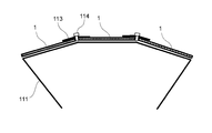
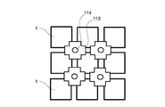
- 12 and 13 are views showing a method of fixing the micro-hole optical element 1 to the frame 111.
- FIG. 12 shows a cross-sectional view
- FIG. 13 shows a front view.
- FIG. 14 is a diagram showing a second embodiment of the fine hole optical element.
- the through-hole 3 is formed in the curved substrate 22 as in the first embodiment. Since the substrate 22 in the second embodiment is curved along the above-mentioned common spherical surface S, in the micro-hole optical element 20 of the second embodiment, the through-hole 3 extends over a wider range than in the first embodiment. Can be formed, and the field of view of one micro-hole optical element 20 is wide. Note that the curved substrate 22 is easily formed by polishing from a flat glass material, glass molding, or the like.
- FIGS. 15A and 15B are diagrams conceptually showing a third embodiment of a micro-hole optical element.
- FIG. 15A is a front view
- FIG. 15B is a side view.
- the micro-hole optical element 30 of the third embodiment is a so-called Schmidt-type lobster eye-type optical element (LEO), and has a transparent substrate 32 having a rectangular outer shape with a side of, for example, 40 mm and a thickness of, for example, 1 mm.
- the upper slit hole 33a and the lower slit hole 33b each having a depth of, for example, 0.5 mm are formed.
- the material of the transparent substrate 32 is the same as in the first embodiment.
- Each slit hole 33a, 33b has a slit width of, for example, 20 ⁇ m, and a glass or resin portion located between the slit holes 33a, 33b has a width of, for example, 6 ⁇ m.
- FIG. 16 is an enlarged perspective view of a portion P in FIG. 15B.
- the upper slit hole 33a and the lower slit hole 33b extend, for example, in directions orthogonal to each other. Further, through the two-stage slit holes 33a and 33b, a through hole is substantially formed in the transparent substrate 32.
- a reflective layer similar to that of the first embodiment is formed on the inner wall of each of the slit holes 33a and 33b, but is not shown.
- the inner wall of the upper slit hole 33a of the two slit holes 33a and 33b reflects light in the same manner as the laterally opposed inner wall of FIG. 4, and the lower slit hole of the two slit holes 33a and 33b.
- the inner wall 33b reflects light in the same manner as the vertically opposed inner wall in FIG.
- the microhole optical element 30 according to the third embodiment which is a Schmitt-type LEO, a cross-shaped light-condensing pattern as shown in FIG. 5 is obtained.
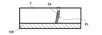
- FIG. 17 is a diagram showing a first procedure in the reforming step.
- the reforming is performed on a portion corresponding to the lower slit hole 33b located on the front side in the incident direction of the pulse laser PL among the two slit holes 33a and 33b.
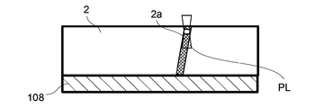
- FIG. 18 is a diagram showing a second procedure in the reforming step.
- the portion corresponding to the upper slit hole 33a located on the near side in the incident direction of the pulse laser PL is modified. Is done. As described above, the portion of the slit hole 33a located on the near side in the incident direction of the pulse laser PL is modified later, so that the progress of the pulse laser PL is disturbed at the modified portion of the transparent substrate 32. Thus, the reforming is performed with high positional accuracy.
- the transparent substrate 32 modified by the procedure shown in FIGS. 17 and 18 is then subjected to the steps (B) to (D) shown in FIGS. 7B to 7D, whereby the Schmidt-type microhole optical element 30 is formed. Almost manufactured.
- the pulse laser PL is irradiated from one of the two surfaces of the transparent substrate 32, it is desirable that the labor of turning the transparent substrate 32 upside down and the time of positioning be omitted.
- the reforming step according to the present invention may be a step of reforming by irradiating a pulse laser PL to each of the two-stage slit holes 33a and 33b from both sides of the transparent substrate 32.
- the micro-hole optical element 30 according to the third embodiment manufactured as described above may be attached to the optical device 100 shown in FIG. 10 instead of the micro-hole optical element 1 according to the first embodiment. Even when the Schmidt-type microhole optical element 30 is attached to the optical device 100 shown in FIG. 10, a device with a wide field of view can be easily obtained.
- the hole forming step according to the present invention a hole forming step including a modification step using a laser and a removing step is shown.
- the hole forming step according to the present invention is, for example, opaque.
- the process may be a process in which holes are directly formed on the substrate by laser processing or the like without going through a reforming process, or a hole forming process including a reforming process by means other than laser irradiation.
- micro-hole optical element used for astronomical observation is illustrated, but the micro-hole optical element according to the present invention may be used for observation and imaging of non-astronomical objects.
- the micro-hole optical element may be one in which slit holes or inner walls intersect at an angle other than orthogonal.
- the substrate according to the present invention may be, for example, a substrate in which a plurality of substrate portions are stacked in a thickness direction or a plurality of substrate portions in a spreading direction. May be a joined substrate.
Landscapes
- Physics & Mathematics (AREA)
- Spectroscopy & Molecular Physics (AREA)
- Engineering & Computer Science (AREA)
- General Engineering & Computer Science (AREA)
- High Energy & Nuclear Physics (AREA)
- General Physics & Mathematics (AREA)
- Optics & Photonics (AREA)
- Optical Elements Other Than Lenses (AREA)
- Laser Beam Processing (AREA)
Abstract
LEOを、品質が安定し且つ簡便に製造する。 微細穴光学素子の製造方法の一態様は、基板に複数の穴が並んで穿たれ、各穴の深さ方向の延長線が基板外に位置した共通の交点へと向かうとともに、各穴は当該交点を中心とした共通の球面と交わる微細穴光学素子の製造方法であって、上記基板に対して上記複数の穴を形成する穴形成工程と、上記複数の穴それぞれの内壁に反射層を形成する反射層形成工程と、を備える。
Description
本発明は、微細穴光学素子の製造方法および光学装置に関する。
X線は、可視光とは異なり、直入射光学系の利用が困難である。このため、金属のX 線に対する屈折率が1よりも小さいことを利用した金属面の全反射による斜入射光学系が用いられている。この場合の全反射の臨界角は1度程度と小さいため、反射面の有効面積を大きくとるために、直径の異なる金属製の円筒状の反射鏡を、同軸状に多数配置する方法が知られている。しかしながら、この方法ではX線反射装置全体の重量が増大するため(1m2あたり1トン以上の重量)、宇宙空間で利用する場合に、地上からの輸送に支障を来すという問題があった。
特許文献1(特許第4025779号公報)には、軽量かつ比較的容易に製造できるX線光学系基材として、異方性エッチングによるシリコンウェハ壁面をX線反射鏡として利用するX線光学系基材が提案されている。これは、薄いウェハに微細な穴を開けるため、従来よりも一桁以上軽い鏡となるうえ、一度のエッチングにより鏡を大量に生産できるという利点もある。しかし、異方性エッチングで形成できる穴は、直線的なスリット状の穴に限られるため、X線光学系を作る際には、反射鏡としての理想曲面を直線で近似する必要があり、集光性能が制限される。また、理想曲面に近づけるため、X線光学系を小さくして理想曲面に沿って配置することになるので、多数のX線光学系が必要になり、製作に要する労力・コストが大きい。
また、天球上のどの方角から素子を見た場合にもミラー面が存在する光学素子として、ロブスターアイ型光学素子(LEO)が知られている。LEOは、特許文献1(特許第4025779号公報)に記載のウォルター型光学系に比べ、観測範囲が広いことが利点である。
特許文献2(特表2009-503506号公報)には、ロブスターアイ型光学素子(LEO)の構成例が開示されている。また、従来、天文学的な物体、すなわち無限遠(x=∞)に存在する物体の観測に使用されていたLEOを、非天文学的な物体、すなわちLEOのレンズ半径Rと比較可能な有限の距離(x~R)に存在する物体の撮影に応用することが記載されている。
従来のLEOの製造方法は、下記工程を経て製造される。
工程1.中実のコア材および中空のクラッド材を準備する。
工程2.クラッド材の内部にコア材を挿入して一体化し、アセンブリを複数作成する。
工程3.複数のアセンブリを引き延ばしつつ束ねて積層体を形成する。
工程4.工程3で得た積層体を軸方向に対し直交方向に薄くスライスした後に、所定の曲率を持つように曲げる。
なお、上記3および4の工程に代えて、以下の工程を実施する場合もある。
工程3´.工程2で得た複数のアセンブリを束ねた積層体を所定の曲率を持つように曲げる。
工程4´.工程3´後の積層体を軸方向に対し直交方向に薄くスライスする。
工程1.中実のコア材および中空のクラッド材を準備する。
工程2.クラッド材の内部にコア材を挿入して一体化し、アセンブリを複数作成する。
工程3.複数のアセンブリを引き延ばしつつ束ねて積層体を形成する。
工程4.工程3で得た積層体を軸方向に対し直交方向に薄くスライスした後に、所定の曲率を持つように曲げる。
なお、上記3および4の工程に代えて、以下の工程を実施する場合もある。
工程3´.工程2で得た複数のアセンブリを束ねた積層体を所定の曲率を持つように曲げる。
工程4´.工程3´後の積層体を軸方向に対し直交方向に薄くスライスする。
しかし、このような製造方法は、アセンブリを束ねる工程や、積層体をスライス後に曲げる工程において、素子に力学的な変形が生じるので品質が安定しないという問題があった。品質に問題がある場合は、結像イメージが理想的な十字形状から崩れる。
そこで、本発明は、LEOを、品質が安定し且つ簡便に製造することを課題とする。
そこで、本発明は、LEOを、品質が安定し且つ簡便に製造することを課題とする。
上記課題を解決するために、本発明に係る微細穴光学素子の製造方法の一態様は、基板に複数の穴が並んで穿たれ、各穴の深さ方向の延長線が基板外に位置した共通の交点へと向かうとともに、各穴は当該交点を中心とした共通の球面と交わる微細穴光学素子の製造方法であって、上記基板に対して上記複数の穴を形成する穴形成工程と、上記複数の穴それぞれの内壁に反射層を形成する反射層形成工程と、を備える。
このような微細穴光学素子の製造方法によれば、基板に穴を形成することでLEOを作成することができる。また、基板に対する力学的な変形が生じないためLEO素子の品質が安定する。更には、従来のようなアセンブリが不要であると共に、積層体のスライスも不要であるので製造が容易である。なお、基板に対する穴の形成としては、例えば後述するようなビームによる方法など簡便な方法が採用可能である。
上記微細穴光学素子の製造方法において、上記基板が透明基板であって、上記穴形成工程が更に、上記穴が形成される箇所について上記透明基板中にビームを照射して多光子吸収を生じさせることで改質する改質工程と、上記改質工程で改質された箇所を除去して上記穴を形成する除去工程とを備えてもよい。改質工程と除去工程とを備えることにより、アスペクト比の高い穴の形成が容易であり、ビーム照射による多光子吸収は透明基板中での位置分解能が高いので精細な穴形状が容易に実現される。
また、上記微細穴光学素子の製造方法は、上記基板が平板状の基板であってもよい。平板状の基板であると穴の形成位置の制御などが容易である。
また、上記微細穴光学素子の製造方法は、上記基板が平板状の基板であってもよい。平板状の基板であると穴の形成位置の制御などが容易である。
また、上記微細穴光学素子の製造方法は、上記基板が上記共通の球面に沿って湾曲した基板であってもよい。共通球面に沿った湾曲基板であると、基板1枚で得られる視野範囲が広い。
また、上記穴形成工程は、上記基板の表面から裏面まで貫通した、断面形状が四角形の貫通穴を形成してもよい。このような四角形の貫通穴が形成されることでいわゆるエンジェル型のLEOが得られる。
また、上記穴形成工程は、上記基板の上記表面に沿って線状に延びた複数の第1スリット穴を当該基板の厚み方向の途中まで形成すると共に、当該基板の上記裏面に沿って当該複数の第1スリット穴に交わる方向に線状に延びた複数の第2スリット穴を当該途中から当該基板の裏面まで形成してもよい。このように第1スリット穴と第2スリット穴が形成されることにより、いわゆるシュミット型のLEOが得られる。また、エンジェル型の四角穴に較べ、シュミット型のスリット穴の方が高い加工精度で形成可能である。
また、上記微細穴光学素子の製造方法において、上記基板が透明基板であって、上記穴形成工程が更に、上記穴が形成される箇所について上記透明基板中にビームを照射して多光子吸収を生じさせることで改質する改質工程と、上記改質工程で改質された箇所を除去して上記穴を形成する除去工程とを備え、上記改質工程が、上記基板の表裏面のうち片面側からビームを照射して上記第1スリット穴と上記第2スリット穴との双方の箇所を改質してもよい。上記第1スリット穴と上記第2スリット穴との双方が基板の片面側から改質されることにより、基板を裏返す工程などが省略されるので工程数が減少する。
また、このように上記第1スリット穴と上記第2スリット穴との双方が基板の片面側から改質される微細穴光学素子の製造方法においては、上記改質工程が、上記第1スリット穴と上記第2スリット穴とのうち、上記ビームの進行方向前方側に位置するスリット穴の箇所から先に改質することが好ましい。この製造方法によれば、改質済みの箇所によるビームの乱れが回避されるので改質箇所の精度が向上する。
また、上記微細穴光学素子の製造方法において、上記反射層形成工程を経た複数の上記基板を支持フレーム上に並べて固定する固定工程を備えることも好ましい。固定工程を備えることにより、多数の基板を当該基板の面方向に沿って敷き詰めることで、広視野の光学装置が容易に得られる。
本発明に係る光学装置の一態様は、基板に複数の穴が並んで穿たれ、各穴の深さ方向の延長線が基板外に位置した共通の交点へと向かうとともに、各穴は当該交点を中心とした共通の球面と交わる微細穴光学素子と、上記微細穴光学素子からの通過光が抜ける枠穴が複数穿たれ、各枠穴を囲った各枠で各微細穴光学素子を支持する支持フレームと、を備える。
このような構成の光学装置によれば、多数の基板を当該基板の面方向に沿って敷き詰めることで、広い視野の装置が容易に得られる。
このような構成の光学装置によれば、多数の基板を当該基板の面方向に沿って敷き詰めることで、広い視野の装置が容易に得られる。
本発明に係る光学装置の別の一態様は、基板に複数の穴が並んで穿たれ、各穴の深さ方向の延長線が基板外に位置した共通の交点へと向かうとともに、各穴は当該交点を中心とした共通の球面と交わる微細穴光学素子と、複数の上記微細穴光学素子を、上記共通の球面に沿って並べて支持する支持フレームと、を備える。
このような構成の光学装置によれば、広い視野で品質が安定した装置が得られる。
このような構成の光学装置によれば、広い視野で品質が安定した装置が得られる。
本発明の微細穴光学素子の製造方法によれば、LEOを、品質が安定し且つ簡便に製造することができる。
上記した本発明の目的、態様及び効果並びに上記されなかった本発明の目的、態様及び効果は、当業者であれば添付図面及び請求の範囲の記載を参照することにより下記の発明を実施するための形態(発明の詳細な説明)から理解できるであろう。
上記した本発明の目的、態様及び効果並びに上記されなかった本発明の目的、態様及び効果は、当業者であれば添付図面及び請求の範囲の記載を参照することにより下記の発明を実施するための形態(発明の詳細な説明)から理解できるであろう。
以下、本発明の実施の形態を図面に基づいて説明する。
図1Aおよび図1Bは、微細穴光学素子の第1実施形態を概念的に示す図である。図1Aは、正面図、図1Bは、側面図である。
図1Aおよび図1Bは、微細穴光学素子の第1実施形態を概念的に示す図である。図1Aは、正面図、図1Bは、側面図である。
微細穴光学素子1は、一辺が例えば40mmで厚さが例えば0.5mm以上5mm以下の方形状の外形を有した透明基板2に対して多数の四角形状の貫通穴3が縦横に並べられて配備された構造となっている。透明基板2は例えばガラスや透明樹脂などからなり、特に溶融石英のガラスであると、後述する製造方法における貫通穴3の加工が容易となる。
貫通穴3は、本発明にいう穴の一例に相当する。なお、本発明にいう穴は、スリット状の穴であってもよく、基板の途中で他の穴に繋がった穴であってもよい。
貫通穴3は、本発明にいう穴の一例に相当する。なお、本発明にいう穴は、スリット状の穴であってもよく、基板の途中で他の穴に繋がった穴であってもよい。
図1Aでは貫通穴3の密度が実際よりも粗く描かれており、実際の貫通穴3は穴の幅が20μm以上200μm以下に形成されるとともに、貫通穴3相互間に位置するガラスや樹脂の部分の幅が6μm以上30μm以下に形成されている。
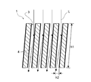
図2は、図1B中の部分Pにおける拡大断面図である。
図2は、図1B中の部分Pにおける拡大断面図である。
微細穴光学素子1の各貫通穴3は、微細穴光学素子1の表側(図1Bの上方)から裏側(図1Bの下方)へと貫通しており、微細穴光学素子1に対して表側からX線や真空紫外線などの光Lが入射し、裏側から光Lが出射する。各貫通穴3における光Lの進行方向の長さh1と、光Lがスリット3から出射する箇所における穴の幅h2との比h1/h2は例えば20以上50以下という大きな値となっている。
各貫通穴3の内壁には金属の反射層4が形成されている。反射層4は例えば酸化ハフニウム等の重金属からなる単層膜や多層膜である。各貫通穴3に入射した光Lは、貫通穴3に対する光Lの入射角度に応じて0~2回、反射層4で反射される。
反射層4の材料の例としては、上記の酸化ハフニウムのほか、酸化物では、酸化タンタル、酸化チタニウム、酸化ランタン、酸化亜鉛等、窒化物では、窒化チタン、窒化タンタル、窒化ハフニウム等、金属では、ルビジウム、銅、タングステン、モリブデン、白金、イリジウム、金が挙げられる。単層膜の反射層4は、例えば数百~数千Åの膜厚で形成される。
また、反射層4は、重金属から成る薄膜と軽金属から成る薄膜から構成される多層膜であってもよく、この場合の最外層は、重金属から成る薄膜で構成される。軽金属から成る薄膜としては例えば酸化アルミニウムが用いられるが、その他に酸化珪素が用いられてもよい。更に、反射層4は、白金/炭素、モリブデン/珪素、タングステン/珪素等と言ったペア材料の多層膜であってもよい。これらのペア材料による多層膜の場合、1ペアについて例えば数十Åの膜厚で数十~数百層が積層されて形成される。
微細穴光学素子1はいわゆるエンジェル型のロブスターアイ型光学素子(LEO)となっており、光Lを焦点に集めることができる。
図3は、微細穴光学素子1における各貫通穴3の向きを示す図である。
微細穴光学素子1はいわゆるエンジェル型のロブスターアイ型光学素子(LEO)となっており、光Lを焦点に集めることができる。
図3は、微細穴光学素子1における各貫通穴3の向きを示す図である。
微細穴光学素子1における各貫通穴3は、深さ方向の各延長線Mが、各貫通穴3に対して共通の交点Pを向いている。この結果、各延長線Mは共通の交点Pに集まる。また、この共通の交点Pを中心とする半径が100mm以上1000mm以下の球面Sが各貫通穴3と交わっている。このような貫通穴3の配置が、いわゆるロブスターアイ型光学素子(LEO)における配置であり、各貫通穴3の内壁で反射された光が以下説明するように集光される。
図4は、LEOにおける集光作用の説明図である。
図4は、LEOにおける集光作用の説明図である。
LEOである微細穴光学素子1では、上述したように、貫通穴3の内壁(の反射層4)で光Lが0~2回反射され、反射パターンに応じた集光パターンで光Lが集光される。ここで、微細穴光学素子1には同一方向から平行に光Lが入射するものとする。同一方向から平行に微細穴光学素子1へと入射した光Lであっても、入射した箇所によって反射パターンが変わる。
例えば、貫通穴3の内壁で0回反射された光Ld(即ち反射されずに貫通穴3を通過した光Ld)は、入射方向へとそのまま進んで焦点面FP上の各所に、集光されずに到達する。
また、貫通穴3の内壁のうち、図の横方向に向かい合った内壁で1回反射された光Lbは、図の横方向について集光され、図の縦方向については入射方向のままとなるので、図の縦方向へと延びる線状の領域に集光される。
また、貫通穴3の内壁のうち、図の縦方向(紙面の奥行方向)に向かい合った内壁で1回反射された光Lcは、図の縦方向について集光され、図の横方向については入射方向のままとなるので、図の横方向へと延びる線状の領域に集光される。
また、貫通穴3の内壁で2回反射された光La(即ち、図の縦方向に向かい合った内壁と図の横方向に向かい合った内壁とで1回ずつ反射された光La)は、縦横両方向で集光されるので中心箇所に点状に集光される。
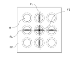
図5は、LEOにおける理想的な集光イメージを示す図である。
図5は、LEOにおける理想的な集光イメージを示す図である。
上述した反射パターンの結果、同一の入射方向から微細穴光学素子1へと入射した光束は、集光面FP上に、十字形状の集光イメージを形成する。即ち、集光面FP上には、十字形状の背景の各所に広がるハローHと、十字の縦横を成す集光ラインFLと、十字の中心に位置する集光スポットFSとが形成される。このような集光イメージが受光装置で測定されることにより、例えば点光源からの光が検出される。
図6は、微細穴光学素子1へと異なる方向から入射した光の集光形態を示す図である。
ここでは一例として、3方向のそれぞれから微細穴光学素子1へと入射した光L1,L2,L3が示されている。
図6は、微細穴光学素子1へと異なる方向から入射した光の集光形態を示す図である。
ここでは一例として、3方向のそれぞれから微細穴光学素子1へと入射した光L1,L2,L3が示されている。
各方向からの光L1,L2,L3は、上述した共通の球面Sと交わる各貫通穴3の反射層4によって反射されることにより、焦点面FP上の異なる箇所に集光される。集光された各箇所において、上述した十字形状の集光パターンが形成される。
共通の球面Sと交わる各貫通穴3は、言い換えると、球面Sに沿って並んでいることになり、焦点面FPは球面状となっている。また、焦点面FPの半径は、共通の球面Sにおける半径Rの半分となる。
このように、LEOである微細穴光学素子1は、各方向から入射してくる光L1,L2,L3の何れについても同様に集光することができるので視野が広い。
次に、このような微細穴光学素子1の製造工程について説明する。
図7A~図7Dは、微細穴光学素子1の製造工程を示す図である。
図7A~図7Dに示す製造工程は、それぞれ改質工程(A)、エッチング工程(B)、研磨工程(C)、反射層形成工程(D)である。
このように、LEOである微細穴光学素子1は、各方向から入射してくる光L1,L2,L3の何れについても同様に集光することができるので視野が広い。
次に、このような微細穴光学素子1の製造工程について説明する。
図7A~図7Dは、微細穴光学素子1の製造工程を示す図である。
図7A~図7Dに示す製造工程は、それぞれ改質工程(A)、エッチング工程(B)、研磨工程(C)、反射層形成工程(D)である。
改質工程(A)では、透明基板2にパルスレーザ光PLが照射され、パルスレーザ光PLによって透明基板2が改質される。パルスレーザ光PLの照射エリアの形状・位置・角度はCADデータに基いて決定される。
本実施形態では、透明基板2の改質は、パルスレーザ光PLにおける多光子吸収によって実現される。透明基板2中で多光子吸収が起きると多光子吸収を起こした部分が特異的に改質される。透明基板2が例えばガラス基板である場合は、珪素(Si)原子と酸素(O)原子との結合による局所構造が多光子吸収によって分断されて構造変化等が生じ、化学的に反応しやすい状態となる。また、改質に必要なエネルギーは、アブレーションなどといった破壊的な作用を生じるレーザ加工に必要なエネルギーよりも少なくて済む。改質工程(A)については後で詳述する。
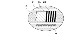
エッチング工程(B)では、透明基板2がエッチャント5に浸され、エッチング処理によって改質領域2aが選択的に除去される。透明基板2が例えばガラス基板である場合は、エッチャント5として弗酸(HF)溶液や水酸化カリウム溶液が用いられる。
本実施形態では、エッチング処理として、処理の手間が少ないウェットエッチングが採用されているが、エッチング処理としてはフッ素(F2)系ガスを用いたドライエッチングも採用可能である。また、本実施形態では、処理の安定化や迅速化のために、エッチャント5中の透明基板2に対して超音波Wを当てる超音波洗浄も併用される。エッチングの条件は、HF濃度が例えば2.5~5%であり、透明基板2のサイズによって異なるがエッチング時間は例えば1時間~数時間である。
エッチング工程(B)では、改質領域2a以外の部分についてもエッチャント5と透明基板2が反応するが、改質領域2aと、改質領域2a以外の領域2bとではエッチングレートが大きく異なる。このため、エッチング工程(B)の開始後速やかに改質領域2aは完全に除去されて貫通穴3が形成される。なお、ここに示す例では、透明基板2に貫通穴3が形成されるので改質領域2aは透明基板2を貫いて形成されるが、透明基板2に有底のスリット(非貫通穴)が形成される場合であれば、改質領域2aは透明基板2の表面に一端のみが達するように形成される。
このように、パルスレーザを用いた多光子吸収現象を利用した改質工程(A)とエッチング工程(B)とを経ることにより、貫通穴3の形状・深さ等を簡単にコントロールすることができ、しかも、基板に対して、物理的な穴あけ加工を行う場合に比べて、基板へのダメージが少ない。
研磨工程(C)では、各貫通穴3の側壁を平滑化するために、磁性流体と研磨材との混合液6が用いられる。磁性流体は、磁場が印加されることで粘性が変化する流体であり、既に光学部品の研磨などに実用化されている。具体的には、平均粒径が約0.01μmの磁性流体と、粒径が例えば1μmのダイヤモンドスラリーとの混合液6が各貫通穴3に流し込まれ、透明基板2と垂直に変動磁場が印加される。
混合液6は磁場の変動に合わせて貫通穴3内をランダムに移動する。透明基板2を中心軸の周りに回転させて、混合液6と貫通穴3の側壁との相対運動を促進することも可能である。混合液6が各貫通穴3の側壁面を研磨することにより、側壁面の粗さが平滑化され、例えば1~2nmの面粗さが実現される。
反射層形成工程(D)では、透明基板2が金属蒸気と反応物質との混合気体7中に置かれ、原子層堆積(ALD)法によって貫通穴3の内壁に金属の反射層4が形成される。原子層堆積法では、貫通穴3の内壁全体に原子層が1層ずつ形成されるので、アスペクト比の高い貫通穴3であっても反射層4が均等に形成される。
上記改質工程(A)とエッチング工程(B)と研磨工程(C)とを併せたものが、本発明にいう穴形成工程の一例に相当し、上記反射層形成工程(D)が、本発明にいう反射層形成工程の一例に相当する。また、上記改質工程(A)は、本発明にいう改質工程の一例に相当し、上記エッチング工程(B)は、本発明にいう除去工程の一例に相当する。
このような製造方法により、図1Aおよび図1Bに示す微細穴光学素子1が実現される。
次に、上述した改質工程(A)について更に詳しく説明する。
図8は、図7Aに示す改質工程(A)を実行するレーザ改質装置10の構造を示す図である。
このような製造方法により、図1Aおよび図1Bに示す微細穴光学素子1が実現される。
次に、上述した改質工程(A)について更に詳しく説明する。
図8は、図7Aに示す改質工程(A)を実行するレーザ改質装置10の構造を示す図である。
レーザ改質装置10は、パルスレーザ光を発するレーザ発振器101を備えている。レーザ発振器101としては、パルス幅が例えば200fs以上500fs以下で、パルスエネルギーが1μJ以下で、繰り返し周波数が5MHz以下のものが用いられる。このようなレーザ発振器101は、高ピークパワーを持った超短パルスのレーザ光を発するので、そのパルスレーザ光がガラスなどの透明基板2に集光されることで容易に多光子吸収等の非線形効果を生じる。
レーザ改質装置10は、パルスレーザ光を改質に適したエネルギーに減光するためのアテネータ103を備えている。また、加工物(ワーク)である透明基板2上で必要なスポットサイズが得られるように、ビーム拡大系104と絞り用レンズ(fθレンズ)106が備えられている。この結果、集光系のNA値は例えば0.26などといった大きな値となる。
レーザ改質装置10は、透明基板2上の指定された箇所に指定された角度の貫通穴、もしくは非貫通穴を形成させるため、透明基板2を立体的に移動させるXYZ軸ステージ108を備えるとともに、パルスレーザ光をスキャンする2軸のガルバノミラー105も備えている。これらXYZ軸ステージ108およびガルバノミラー105によってパルスレーザ光は透明基板2中の指定された箇所に集光されて集光スポットを形成する。
図9A~図9Eは、レーザ改質装置10で実行される改質工程(A)の手順例を示す図である。
図9A~図9Eには、改質工程(A)で透明基板2中に改質領域2aが形成される手順の一例として、段階(A)から段階(E)までの手順が模式的に示されている。
図9A~図9Eは、レーザ改質装置10で実行される改質工程(A)の手順例を示す図である。
図9A~図9Eには、改質工程(A)で透明基板2中に改質領域2aが形成される手順の一例として、段階(A)から段階(E)までの手順が模式的に示されている。
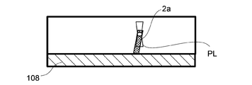
図9Aの段階(A)では、XYZ軸ステージ108が、CADデータに基づいたスタート箇所に位置決めされることで、透明基板2の裏面直上にパルスレーザPLの焦点が結ばれ、改質領域2aの形成が開始される。
図9Bの段階(B)では、XYZ軸ステージ108が図の下方へと移動することでパルスレーザPLの焦点が透明基板2の内部側へと移動し、その結果、改質領域2aが透明基板2の内部側に延びる。
図9Cの段階(C)および図9Dの段階(D)では、更にXYZ軸ステージ108が移動して改質領域2aが透明基板2の表面側へと更に延びていく。
図9Cの段階(C)および図9Dの段階(D)では、更にXYZ軸ステージ108が移動して改質領域2aが透明基板2の表面側へと更に延びていく。
図9Eの段階(E)では、XYZ軸ステージ108がエンド箇所まで移動し、パルスレーザPLの焦点が透明基板2の表面直下まで達する。これにより、透明基板2の表面から裏面に至る改質領域2aが形成される。
以上の手順で、図1Aに示すように配列された貫通穴3のうち、透明基板2上の1箇所に相当する部分が改質される。従って、図9A~図9Eに示す手順が、透明基板2上の各所で繰り返されることで、図1Aに示すように配列され図2に示すような断面形状と図3に示すような各向きとを有した各貫通穴3に相当する改質領域2aが形成されることになる。なお、本実施形態の微細穴光学素子1は、平板状の基板2を有するので、XYZ軸ステージ108によるパルスレーザPLの焦点位置の制御が容易である。
このように、本実施形態の微細穴光学素子1の製造方法では、理想的な形状と向きを有する貫通穴3(および反射層4)が簡便な工程で透明基板2に高精度に形成され、貫通穴3(および反射層4)の形成に際して透明基板2には応力などが加えられない。このため微細穴光学素子1は、広い視野を有するとともに結像性能(品質)も高い。
次に、このように製造される微細穴光学素子1が組み込まれた光学装置について説明する。
図10は、微細穴光学素子1が組み込まれた光学装置100を示す図である。
光学装置100は例えば天体を観測する装置であり、光学系部分110と電子系部分120とを備えている。
次に、このように製造される微細穴光学素子1が組み込まれた光学装置について説明する。
図10は、微細穴光学素子1が組み込まれた光学装置100を示す図である。
光学装置100は例えば天体を観測する装置であり、光学系部分110と電子系部分120とを備えている。
電子系部分120は、光学系部分110に対向する位置に受光装置121を備えている。受光装置121の受光面は、上述した焦点面FPに沿った球面状の面である。また、電子系部分120の本体部分122には、受光装置121の電源や制御回路などが組み込まれている。
光学系部分110はフレーム111を有し、そのフレーム111上に複数の微細穴光学素子1が並べて固定され、それら複数の微細穴光学素子1がフレーム111で支持されている。
図11は、光学装置100の光学系部分110の組み立て図である。
図11は、光学装置100の光学系部分110の組み立て図である。
フレーム111には枠穴112が設けられており、各枠穴112に各微細穴光学素子1が対応付けられて微細穴光学素子1が取り付けられる。各微細穴光学素子1からの通過光は、フレーム111の枠穴112を通り抜け、受光装置121の受光面上に上述した集光パターンで集光される。
フレーム111が各微細穴光学素子1を支持する部分の全体的な形状は、上述した共通の球面Sに沿った球面状の形状となっており、各微細穴光学素子1は共通の球面Sに沿った球面状に並べられて支持される。この結果、複数の微細穴光学素子1の全体で1つのLEOとして機能し、例えば30度といった広い視野が実現される。つまり、平板状の微細穴光学素子1が球面状に配置されることにより、製造が容易で広視野の光学装置が実現される。
図12,図13は、フレーム111に対する微細穴光学素子1の固定方法を示す図であり、図12には断面図が示され、図13には正面図が示されている。
図12,図13は、フレーム111に対する微細穴光学素子1の固定方法を示す図であり、図12には断面図が示され、図13には正面図が示されている。
微細穴光学素子1は、四角形の角の部分が押さえ部材113によって押さえられ、押さえ部材113はピン114によってフレーム111に固定される。このような固定構造により、微細穴光学素子1は、貫通穴3が設けられて集光に寄与する領域が光に対して広く露出した状態でフレーム111に固定される。
次に、微細穴光学素子の第2実施形態について説明する。
図14は、微細穴光学素子の第2実施形態を示す図である。
次に、微細穴光学素子の第2実施形態について説明する。
図14は、微細穴光学素子の第2実施形態を示す図である。
第2実施形態の微細穴光学素子20では、湾曲した基板22に、第1実施形態と同様に貫通穴3が形成されている。第2実施形態における基板22は、上述した共通の球面Sに沿って湾曲しているので、第2実施形態の微細穴光学素子20では、第1実施形態よりも広い範囲に亘って貫通穴3が形成可能であり、1枚の微細穴光学素子20における視野が広い。なお、湾曲した基板22は、平板状のガラス材料からの研磨やガラスモールドなどによって容易に形成される。
次に、微細穴光学素子の第3実施形態について説明する。
図15Aおよび図15Bは、微細穴光学素子の第3実施形態を概念的に示す図である。図15Aは、正面図、図15Bは、側面図である。
次に、微細穴光学素子の第3実施形態について説明する。
図15Aおよび図15Bは、微細穴光学素子の第3実施形態を概念的に示す図である。図15Aは、正面図、図15Bは、側面図である。
第3実施形態の微細穴光学素子30は、いわゆるシュミット型のロブスターアイ型光学素子(LEO)となっており、一辺が例えば40mmで厚さが例えば1mmの方形状の外形を有した透明基板32に対して各々の深さが例えば0.5mmの上段のスリット穴33aと下段のスリット穴33bが形成された構造となっている。透明基板32の材質は第1実施形態と同様である。
各スリット穴33a,33bのスリット幅は例えば20μmに形成され、スリット穴33a,33bの相互間に位置するガラスや樹脂の部分の幅が例えば6μmに形成されている。
図16は、図15B中の部分Pにおける拡大斜視図である。
図16は、図15B中の部分Pにおける拡大斜視図である。
上段のスリット穴33aと下段のスリット穴33bは、例えば互いに直交する方向に延びている。また、2段のスリット穴33a,33bを経ることで、実質的に貫通穴が透明基板32に形成されている。また、各スリット穴33a,33bの内壁には第1実施形態と同様の反射層が形成されているが図示は省略されている。
2段のスリット穴33a,33bのうち上段のスリット穴33aの内壁は、図4の横方向に対向した内壁と同様に光を反射し、2段のスリット穴33a,33bのうち下段のスリット穴33bの内壁は、図4の縦方向に対向した内壁と同様に光を反射する。この結果、シュミット型のLEOである第3実施形態の微細穴光学素子30でも、図5に示すような十字型の集光パターンが得られる。
このようなシュミット型のLEOである第3実施形態の微細穴光学素子30は、図7A~図7Dに示す製造工程と同様の製造工程によって製造される。但し、改質工程における手順が第1実施形態とは異なるので、以下、改質工程における手順について説明する。
図17は、改質工程における第1の手順を示す図である。
図17は、改質工程における第1の手順を示す図である。
ここでは一例として、パルスレーザPLが透明基板32の上段側から入射される場合について説明する。図17に示す第1の手順では、2段のスリット穴33a,33bのうち、パルスレーザPLの入射方向で前方側に位置する下段のスリット穴33bに相当する箇所について改質が行われる。
下段のスリット穴33bが延びる方向(即ち図の左右方向)にパルスレーザPLが移動されながら改質が行われることで、スリット穴33bに相当する領域が精度のよい直線状に改質される。
図18は、改質工程における第2の手順を示す図である。
図18は、改質工程における第2の手順を示す図である。
2段のスリット穴33a,33bのうち下段のスリット穴33bに相当する箇所が改質された後、パルスレーザPLの入射方向で手前側に位置する上段のスリット穴33aに相当する箇所が改質される。このように、パルスレーザPLの入射方向で手前側に位置する方のスリット穴33aの箇所が後で改質されることにより、透明基板32の改質済みの箇所でパルスレーザPLの進行が乱される虞が回避され、高い位置精度で改質が行われる。
上段のスリット穴33aが延びる方向(即ち図の上下方向)にパルスレーザPLが移動されながら改質が行われることで、スリット穴33aに相当する領域が精度のよい直線状に改質される。
図17、図18に示す手順で改質された透明基板32が、その後、図7B~図7Dに示す各工程(B)~(D)を経ることで、シュミット型の微細穴光学素子30が容易に製造される。なお、図17、図18に示す手順では、透明基板32の両面のうち片面側からパルスレーザPLが照射されるので、透明基板32を裏返す手間や位置合わせの手間などが省かれて望ましいが、本発明にいう改質工程は、透明基板32の両面それぞれから2段のスリット穴33a,33bそれぞれの箇所にパルスレーザPLを照射して改質する工程であってもよい。
このように製造された第3実施形態の微細穴光学素子30は、図10に示す光学装置100に、第1実施形態の微細穴光学素子1に替えて取り付けられてもよい。シュミット型の微細穴光学素子30が図10に示す光学装置100に取り付けられた場合にも、広視野の装置が容易に得られる。
なお、上記説明では、本発明にいう穴形成工程の一例として、レーザによる改質工程と除去工程とを備える穴形成工程が示されているが、本発明にいう穴形成工程は、例えば不透明な基板に対して改質工程を経ずにレーザ加工などによって穴を直接形成する工程であってもよいし、レーザ照射以外の手段による改質工程を備える穴形成工程であってもよい。
また、上記説明では、天体観測用に用いられる微細穴光学素子が例示されているが、本発明にいう微細穴光学素子は、非天文学的な物体の観測や撮像に用いられてもよい。
また、上記説明では、2段のスリット穴33a,33bそれぞれの延びる方向が互いに直交する例や、四角形の貫通穴の互いに隣り合う内壁同士が互いに直交する例が示されているが、本発明にいう微細穴光学素子は、直交以外の角度でスリット穴同士や内壁同士が交わるものであってもよい。
また、上記説明では、基板として単一形成の基板が例示されているが、本発明にいう基板は、例えば厚さ方向に複数の基板部分が重ねられた基板や、広がり方向に複数の基板部分が継ぎ合わされた基板であってもよい。
なお、上記において特定の実施形態が説明されているが、当該実施形態は単なる例示であり、本発明の範囲を限定する意図はない。本明細書に記載された装置及び方法は上記した以外の形態において具現化することができる。また、本発明の範囲から離れることなく、上記した実施形態に対して適宜、省略、置換及び変更をなすこともできる。かかる省略、置換及び変更をなした形態は、請求の範囲に記載されたもの及びこれらの均等物の範疇に含まれ、本発明の技術的範囲に属する。
1,21,30…微細穴光学素子、2,22,32…透明基板、3…貫通穴、33a,33b…スリット穴、4…反射層、100…光学装置、111…フレーム
Claims (11)
- 基板に複数の穴が並んで穿たれ、各穴の深さ方向の延長線が基板外に位置した共通の交点へと向かうとともに、各穴は当該交点を中心とした共通の球面と交わる微細穴光学素子の製造方法であって、
前記基板に対して前記複数の穴を形成する穴形成工程と、
前記複数の穴それぞれの内壁に反射層を形成する反射層形成工程と、
を備えることを特徴とする微細穴光学素子の製造方法。 - 前記基板が透明基板であって、
前記穴形成工程が更に、
前記穴が形成される箇所について前記透明基板中にビームを照射して多光子吸収を生じさせることで改質する改質工程と、
前記改質工程で改質された箇所を除去して前記穴を形成する除去工程とを備えることを特徴とする請求項1に記載の微細穴光学素子の製造方法。 - 前記基板が平板状の基板であることを特徴とする請求項1または2に記載の微細穴光学素子の製造方法。
- 前記基板が前記共通の球面に沿って湾曲した基板であることを特徴とする請求項1または2に記載の微細穴光学素子の製造方法。
- 前記穴形成工程が、前記基板の表面から裏面まで貫通した、断面形状が四角形の貫通穴を形成することを特徴とする請求項1から4のいずれか1項に記載の微細穴光学素子の製造方法。
- 前記穴形成工程が、前記基板の表面に沿って線状に延びた複数の第1スリット穴を当該基板の厚み方向の途中まで形成すると共に、当該基板の裏面に沿って当該複数の第1スリット穴に交わる方向に線状に延びた複数の第2スリット穴を当該途中から当該基板の裏面まで形成することを特徴とする請求項1から4のいずれか1項に記載の微細穴光学素子の製造方法。
- 前記基板が透明基板であって、
前記穴形成工程が、
前記スリット穴が形成される箇所について前記透明基板中にビームを照射して多光子吸収を生じさせることで当該透明基板を改質する改質工程と、
前記改質工程で改質された箇所を除去して前記スリット穴を形成する除去工程とを備え、
前記改質工程が、前記基板の表裏面のうち片面側からビームを照射して前記第1スリット穴と前記第2スリット穴との双方の箇所を改質することを特徴とする請求項6に記載の微細穴光学素子の製造方法。 - 前記改質工程が、前記第1スリット穴と前記第2スリット穴とのうち、前記ビームの進行方向前方側に位置するスリット穴の箇所から先に改質することを特徴とする請求項7に記載の微細穴光学素子の製造方法。
- 前記反射層形成工程を経た複数の前記基板を支持フレーム上に並べて固定する固定工程を備えることを特徴とする請求項1から8のいずれか1項に記載の微細穴光学素子の製造方法。
- 基板に複数の穴が並んで穿たれ、各穴の深さ方向の延長線が基板外に位置した共通の交点へと向かうとともに、各穴は当該交点を中心とした共通の球面と交わる微細穴光学素子と、
前記微細穴光学素子からの通過光が抜ける枠穴が複数穿たれ、各枠穴を囲った各枠で各微細穴光学素子を支持する支持フレームと、
を備えたことを特徴とする光学装置。 - 基板に複数の穴が並んで穿たれ、各穴の深さ方向の延長線が基板外に位置した共通の交点へと向かうとともに、各穴は当該交点を中心とした共通の球面と交わる微細穴光学素子と、
複数の前記微細穴光学素子を、前記共通の球面に沿って並べて支持する支持フレームと、
を備えたことを特徴とする光学装置。
Applications Claiming Priority (2)
| Application Number | Priority Date | Filing Date | Title |
|---|---|---|---|
| JP2018-154009 | 2018-08-20 | ||
| JP2018154009A JP2020030232A (ja) | 2018-08-20 | 2018-08-20 | 微細穴光学素子の製造方法および光学装置 |
Publications (1)
| Publication Number | Publication Date |
|---|---|
| WO2020039620A1 true WO2020039620A1 (ja) | 2020-02-27 |
Family
ID=69593189
Family Applications (1)
| Application Number | Title | Priority Date | Filing Date |
|---|---|---|---|
| PCT/JP2019/006264 Ceased WO2020039620A1 (ja) | 2018-08-20 | 2019-02-20 | 微細穴光学素子の製造方法および光学装置 |
Country Status (2)
| Country | Link |
|---|---|
| JP (1) | JP2020030232A (ja) |
| WO (1) | WO2020039620A1 (ja) |
Cited By (1)
| Publication number | Priority date | Publication date | Assignee | Title |
|---|---|---|---|---|
| CN113500773A (zh) * | 2021-07-08 | 2021-10-15 | 吉林大学 | 仿龙虾眼聚焦脉冲强光原位成型4d打印装置及方法 |
Families Citing this family (2)
| Publication number | Priority date | Publication date | Assignee | Title |
|---|---|---|---|---|
| JP7196718B2 (ja) * | 2019-03-26 | 2022-12-27 | ウシオ電機株式会社 | 微細穴光学素子の製造方法および改質装置 |
| JP7529195B2 (ja) * | 2020-06-16 | 2024-08-06 | 東京都公立大学法人 | X線素子の製造方法 |
Citations (4)
| Publication number | Priority date | Publication date | Assignee | Title |
|---|---|---|---|---|
| JP4025779B2 (ja) * | 2005-01-14 | 2007-12-26 | 独立行政法人 宇宙航空研究開発機構 | X線集光装置 |
| JP2015007647A (ja) * | 2014-09-03 | 2015-01-15 | 公立大学法人首都大学東京 | X線光学系 |
| JP2015510581A (ja) * | 2011-12-27 | 2015-04-09 | リガク イノベイティブ テクノロジーズ インコーポレイテッド | パターン化されたx線光学素子の製造方法 |
| JP2016031340A (ja) * | 2014-07-30 | 2016-03-07 | 公立大学法人首都大学東京 | X線光学系基材、及びその製造方法 |
-
2018
- 2018-08-20 JP JP2018154009A patent/JP2020030232A/ja active Pending
-
2019
- 2019-02-20 WO PCT/JP2019/006264 patent/WO2020039620A1/ja not_active Ceased
Patent Citations (4)
| Publication number | Priority date | Publication date | Assignee | Title |
|---|---|---|---|---|
| JP4025779B2 (ja) * | 2005-01-14 | 2007-12-26 | 独立行政法人 宇宙航空研究開発機構 | X線集光装置 |
| JP2015510581A (ja) * | 2011-12-27 | 2015-04-09 | リガク イノベイティブ テクノロジーズ インコーポレイテッド | パターン化されたx線光学素子の製造方法 |
| JP2016031340A (ja) * | 2014-07-30 | 2016-03-07 | 公立大学法人首都大学東京 | X線光学系基材、及びその製造方法 |
| JP2015007647A (ja) * | 2014-09-03 | 2015-01-15 | 公立大学法人首都大学東京 | X線光学系 |
Cited By (1)
| Publication number | Priority date | Publication date | Assignee | Title |
|---|---|---|---|---|
| CN113500773A (zh) * | 2021-07-08 | 2021-10-15 | 吉林大学 | 仿龙虾眼聚焦脉冲强光原位成型4d打印装置及方法 |
Also Published As
| Publication number | Publication date |
|---|---|
| JP2020030232A (ja) | 2020-02-27 |
Similar Documents
| Publication | Publication Date | Title |
|---|---|---|
| JP5389266B2 (ja) | 基板加工方法 | |
| JP5389265B2 (ja) | 基板加工方法 | |
| JP5389264B2 (ja) | レーザ加工方法 | |
| US5919607A (en) | Photo-encoded selective etching for glass based microtechnology applications | |
| Yamasaki et al. | Three-dimensional micro-channels in polymers: one-step fabrication | |
| US5050137A (en) | Ultrasonic probe | |
| KR20190065335A (ko) | 비-축대칭 빔 스폿을 이용하여 투명 워크피스를 레이저 가공하기 위한 기기 및 방법 | |
| WO1997015533A9 (en) | Photo-encoded selective etching for glass based microtechnology applications | |
| JP2020030232A (ja) | 微細穴光学素子の製造方法および光学装置 | |
| WO2022252300A1 (zh) | 基于飞秒激光结合超分辨透镜的光纤探针制备装置及方法 | |
| JP2019139190A (ja) | 微細穴光学素子の製造方法、および微細穴光学素子 | |
| JP7196718B2 (ja) | 微細穴光学素子の製造方法および改質装置 | |
| JP2020160260A (ja) | 光学入出力デバイスの製造方法及び光学入出力デバイス | |
| JP2009217249A (ja) | 可変焦点レンズ | |
| US6744030B2 (en) | Optical waveguide probe and manufacturing method of the same, and scanning near-field optical microscope | |
| JP4155160B2 (ja) | 光電気混載基板の製造方法 | |
| JP4260645B2 (ja) | 近視野光ヘッドの製造方法 | |
| JP2003194697A (ja) | グレーティングカップラを有する探針及びその製造方法、該探針を有するプローブ、及び該プローブを有する情報処理装置、表面観察装置、露光装置、該露光装置による光学素子 | |
| JP2005283993A (ja) | 精度自己収束型レンズ形状作成方法およびその方法によって形成された光学素子 | |
| Doi et al. | Ultrathin and lightweight lobster eye optics formed into a single flat substrate | |
| TWI273281B (en) | Fresnel lens structure | |
| TWI898259B (zh) | 用於將光束成像到物體上的方法、使用該方法將開口引入到工件中的方法以及具有光學配置的裝置 | |
| CN116381830B (zh) | 一种集成型仿生复眼模板结构及其制备方法 | |
| JP4902073B2 (ja) | カンチレバーの作製方法 | |
| CN111299840B (zh) | 一种超快激光直写配合激光抛光制备中阶梯光栅的方法 |
Legal Events
| Date | Code | Title | Description |
|---|---|---|---|
| 121 | Ep: the epo has been informed by wipo that ep was designated in this application |
Ref document number: 19852359 Country of ref document: EP Kind code of ref document: A1 |
|
| NENP | Non-entry into the national phase |
Ref country code: DE |
|
| 122 | Ep: pct application non-entry in european phase |
Ref document number: 19852359 Country of ref document: EP Kind code of ref document: A1 |