WO2020036166A1 - SiC単結晶の評価方法及びSiCウェハの製造方法 - Google Patents
SiC単結晶の評価方法及びSiCウェハの製造方法 Download PDFInfo
- Publication number
- WO2020036166A1 WO2020036166A1 PCT/JP2019/031799 JP2019031799W WO2020036166A1 WO 2020036166 A1 WO2020036166 A1 WO 2020036166A1 JP 2019031799 W JP2019031799 W JP 2019031799W WO 2020036166 A1 WO2020036166 A1 WO 2020036166A1
- Authority
- WO
- WIPO (PCT)
- Prior art keywords
- single crystal
- atomic arrangement
- sic
- sic single
- wafer
- Prior art date
- Legal status (The legal status is an assumption and is not a legal conclusion. Google has not performed a legal analysis and makes no representation as to the accuracy of the status listed.)
- Ceased
Links
Images








Classifications
-
- C—CHEMISTRY; METALLURGY
- C30—CRYSTAL GROWTH
- C30B—SINGLE-CRYSTAL GROWTH; UNIDIRECTIONAL SOLIDIFICATION OF EUTECTIC MATERIAL OR UNIDIRECTIONAL DEMIXING OF EUTECTOID MATERIAL; REFINING BY ZONE-MELTING OF MATERIAL; PRODUCTION OF A HOMOGENEOUS POLYCRYSTALLINE MATERIAL WITH DEFINED STRUCTURE; SINGLE CRYSTALS OR HOMOGENEOUS POLYCRYSTALLINE MATERIAL WITH DEFINED STRUCTURE; AFTER-TREATMENT OF SINGLE CRYSTALS OR A HOMOGENEOUS POLYCRYSTALLINE MATERIAL WITH DEFINED STRUCTURE; APPARATUS THEREFOR
- C30B29/00—Single crystals or homogeneous polycrystalline material with defined structure characterised by the material or by their shape
- C30B29/10—Inorganic compounds or compositions
- C30B29/36—Carbides
-
- G—PHYSICS
- G01—MEASURING; TESTING
- G01N—INVESTIGATING OR ANALYSING MATERIALS BY DETERMINING THEIR CHEMICAL OR PHYSICAL PROPERTIES
- G01N23/00—Investigating or analysing materials by the use of wave or particle radiation, e.g. X-rays or neutrons, not covered by groups G01N3/00 – G01N17/00, G01N21/00 or G01N22/00
- G01N23/20—Investigating or analysing materials by the use of wave or particle radiation, e.g. X-rays or neutrons, not covered by groups G01N3/00 – G01N17/00, G01N21/00 or G01N22/00 by using diffraction of the radiation by the materials, e.g. for investigating crystal structure; by using scattering of the radiation by the materials, e.g. for investigating non-crystalline materials; by using reflection of the radiation by the materials
-
- G—PHYSICS
- G01—MEASURING; TESTING
- G01N—INVESTIGATING OR ANALYSING MATERIALS BY DETERMINING THEIR CHEMICAL OR PHYSICAL PROPERTIES
- G01N23/00—Investigating or analysing materials by the use of wave or particle radiation, e.g. X-rays or neutrons, not covered by groups G01N3/00 – G01N17/00, G01N21/00 or G01N22/00
- G01N23/20—Investigating or analysing materials by the use of wave or particle radiation, e.g. X-rays or neutrons, not covered by groups G01N3/00 – G01N17/00, G01N21/00 or G01N22/00 by using diffraction of the radiation by the materials, e.g. for investigating crystal structure; by using scattering of the radiation by the materials, e.g. for investigating non-crystalline materials; by using reflection of the radiation by the materials
- G01N23/2055—Analysing diffraction patterns
-
- G—PHYSICS
- G01—MEASURING; TESTING
- G01N—INVESTIGATING OR ANALYSING MATERIALS BY DETERMINING THEIR CHEMICAL OR PHYSICAL PROPERTIES
- G01N23/00—Investigating or analysing materials by the use of wave or particle radiation, e.g. X-rays or neutrons, not covered by groups G01N3/00 – G01N17/00, G01N21/00 or G01N22/00
- G01N23/20—Investigating or analysing materials by the use of wave or particle radiation, e.g. X-rays or neutrons, not covered by groups G01N3/00 – G01N17/00, G01N21/00 or G01N22/00 by using diffraction of the radiation by the materials, e.g. for investigating crystal structure; by using scattering of the radiation by the materials, e.g. for investigating non-crystalline materials; by using reflection of the radiation by the materials
- G01N23/207—Diffractometry using detectors, e.g. using a probe in a central position and one or more displaceable detectors in circumferential positions
Definitions
- the present invention relates to a method for evaluating a SiC single crystal and a method for manufacturing a SiC wafer.
- This application claims priority based on Japanese Patent Application No. 2018-152317 for which it applied to Japan on August 13, 2018, and uses the content here.
- Silicon carbide (SiC) has a breakdown electric field one order of magnitude higher than silicon (Si) and a band gap three times larger. Further, silicon carbide (SiC) has characteristics such as a thermal conductivity that is about three times higher than that of silicon (Si). Silicon carbide (SiC) is expected to be applied to power devices, high-frequency devices, high-temperature operation devices, and the like.
- SiC epitaxial wafer having an epitaxial film formed on a SiC wafer is used.
- Chemical vapor deposition (SiC) on SiC wafers An epitaxial film provided by Vapor Deposition (CVD) becomes an active region of the SiC semiconductor device.
- CVD Vapor Deposition
- the SiC epitaxial wafer means a wafer after forming an epitaxial film.
- a SiC wafer means a wafer before an epitaxial film is formed.
- Patent Document 1 describes that an epitaxial film formed on a SiC wafer is improved by setting the amount of warpage of the wafer and the amount of deviation of the crystal orientation within a predetermined range.
- Patent Document 2 describes that a high-quality epitaxial film can be obtained by setting the deviation of the growth plane orientation in the wafer plane within a predetermined range.
- the quality of a SiC ingot is evaluated using X-ray topographic analysis (XRT), KOH etching, or the like after cutting an evaluation wafer (Patent Document 3). If the number of SiC wafers and the number of seed crystals to be obtained after sufficiently evaluating the quality of the SiC ingot are determined, the loss amount of the SiC single crystal can be reduced.
- XRT X-ray topographic analysis
- KOH etching KOH etching
- Patent Document 3 it takes time to process the SiC ingot into a wafer for evaluation and evaluate the quality by etching or the like. As a result, a time loss of several weeks occurs between the processing of the SiC ingot and the processing of the SiC wafer.
- the basal plane dislocation (BPD) is one of the killer defects of the SiC wafer, and is a defect that is considered to be one of the causes of the occurrence of the slip generated on the basal plane.
- the present invention has been made in view of the above problems, and has as its object to efficiently provide a high-quality SiC single crystal wafer.
- the present inventors have evaluated the curved state of the atomic arrangement plane (lattice plane) of the SiC single crystal in at least two directions, and can easily obtain a SiC single crystal in which basal plane dislocation (BPD) is not easily generated. It was found that it can be evaluated. Also, by simply evaluating the atomic arrangement plane of the SiC single crystal, it was found that the rough quality of the SiC ingot can be grasped, and the cutting conditions of the SiC ingot and the next growth condition of the single crystal can be quickly fed back. That is, the present invention provides the following means in order to solve the above problems.
- the method for evaluating a SiC single crystal according to the first aspect includes the first direction along the ⁇ 1-100> direction passing through the center of the SiC single crystal in plan view and the SiC single crystal perpendicular to the first direction. And the second direction along the ⁇ 11-20> direction passing through the center in plan view, and the curved state of the atom arrangement surface in at least two directions.
- the curved state of the atomic arrangement plane may be evaluated in at least six directions rotated by 30 ° with respect to the first direction.
- the bending state of the atomic arrangement plane may be evaluated based on whether or not the bending direction of the atomic arrangement plane in the measurement direction matches.
- the bending state of the atomic arrangement surface may be evaluated from a difference between a maximum value and a minimum value of the amount of curvature of the atomic arrangement surface in a measurement direction.
- the curved state of the atomic arrangement plane may be evaluated by X-ray diffraction.
- X-ray diffraction is performed on five or more points in the same direction passing through the center of the SiC single crystal in a plan view, and the curved state of the atomic arrangement plane is determined. May be evaluated.
- the method for slicing the SiC ingot or the growth conditions for the SiC single crystal are determined based on the evaluation results obtained by the method for evaluating a SiC single crystal according to the above aspect.
- FIG. 4 is a view schematically showing a method for manufacturing a SiC wafer according to the embodiment. It is a cross section of an example of a manufacture device used when manufacturing a SiC ingot.
- FIG. 3 is an example of a schematic cross-sectional view of a SiC ingot crystal-grown on a seed crystal. It is the figure which showed typically the quality evaluation method of the SiC ingot concerning this embodiment.
- FIG. 3 is a schematic view of an example of a cut surface obtained by cutting a SiC single crystal constituting a tail or a head along a straight line extending in a [1-100] direction passing through a center in a plan view.
- FIG. 3 is a diagram for specifically explaining an example of a method of measuring the amount of curvature of an atomic arrangement surface.
- FIG. 3 is a diagram for specifically explaining an example of a method of measuring the amount of curvature of an atomic arrangement surface.
- FIG. 3 is a diagram for specifically explaining an example of a method of measuring the amount of curvature of an atomic arrangement surface.
- FIG. 3 is a diagram for specifically explaining an example of a method of measuring the amount of curvature of an atomic arrangement surface.
- An example in which a radius of curvature of an atomic arrangement surface is obtained from a plurality of XRD measurement points will be described.
- FIG. 9 is a diagram for specifically explaining another example of a method for measuring the amount of curvature of an atomic arrangement surface.
- FIG. 9 is a diagram for specifically explaining another example of a method for measuring the amount of curvature of an atomic arrangement surface.
- FIG. 15B is a supplementary diagram for deriving ⁇ / 2 in FIG. 15A. It is a figure for supplementing FIG.
- FIG. 6 is a diagram showing relative values of the amount of curvature d1 in the [1-100] direction and the amount of curvature d2 in the [11-20] direction of a single crystal, and the density of BPD contained in the crystal growth portion. It is the result of having measured the lattice curvature of the head and tail of the SiC ingot. It is the figure which showed typically the quality evaluation method of the conventional SiC ingot.
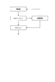
- FIG. 1 is a diagram schematically illustrating a method for manufacturing a SiC wafer according to the present embodiment.
- a seed crystal is prepared.
- SiC is grown on the seed crystal to produce a SiC ingot.
- the obtained SiC ingot undergoes quality evaluation, is processed into a SiC wafer, and is shipped. Further, a part of the SiC ingot is processed into a seed crystal for producing the next SiC ingot.
- the manufactured SiC wafer may be subjected to various processes. For example, when an epitaxial film is formed on the surface of a SiC wafer, it becomes a SiC epitaxial wafer. Further, the SiC epitaxial wafer becomes a SiC device when a part of the epitaxial film is processed.
- FIG. 2 is a schematic cross-sectional view of an example of a manufacturing apparatus used for manufacturing a SiC ingot.
- the manufacturing apparatus 100 shown in FIG. 2 is one of the SiC single crystal manufacturing apparatuses using the sublimation method.
- the sublimation method is a method in which a raw material gas generated by heating a raw material is recrystallized on a single crystal (seed crystal) to obtain a large single crystal (ingot).
- the manufacturing apparatus 100 shown in FIG. 2 includes the crucible 10 and the coil 20. Between the crucible 10 and the coil 20, a heating element (not shown) that generates heat by induction heating of the coil 20 may be provided.
- the crucible 10 has a crystal setting part 11 provided at a position facing the raw material G.
- the crucible 10 may have a taper guide 12 that expands in diameter from the crystal setting part 11 toward the raw material G inside.
- FIG. 2 simultaneously shows the raw material G, the seed crystal 5, and the SiC ingot 6 grown from the seed crystal for easy understanding.
- the crystal growth plane of seed crystal 5 is preferably a carbon plane (C plane) or a plane provided with an off angle of 0 to 10 ° or less from the carbon plane.
- the crystal growth surface of the seed crystal 5 is more preferably a carbon surface or a surface having an off angle of 0 to 5 ° from the carbon surface.
- FIG. 3 is a schematic cross-sectional view of an example of the SiC ingot 6 grown on the seed crystal 5.
- the SiC ingot is generally cut in advance near the crystal growth surface of the SiC ingot 6 (hereinafter, referred to as a head 6A) and the vicinity of the seed crystal 5 (hereinafter, referred to as a tail 6B) before being put into a cutting step such as a multi-wire saw. A process is required.
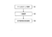
- FIG. 4 is a diagram schematically illustrating a method for evaluating the quality of a SiC ingot according to the present embodiment.
- the tail or head of the SiC ingot is cut and obtained (step S1).
- the step of obtaining the head 6A or the tail 6B or the like is necessary for cutting with a multi-wire saw or the like. Therefore, by using the evaluation method, it is not necessary to newly generate an additional cutting step or to obtain an evaluation sample at the expense of a product obtaining unit.
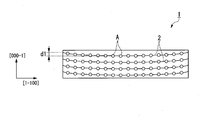
- FIG. 5 is a schematic view of an example of a cut surface obtained by cutting the SiC single crystal constituting the head 6A or the tail 6B along a straight line extending in the [1-100] direction passing through the center in plan view.
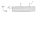
- FIG. 6 is a schematic view of an example of a cut surface obtained by cutting the SiC single crystal constituting the head 6A or the tail 6B along a straight line extending in the [11-20] direction passing through the center in plan view.
- the upper side is the direction in which the carbon plane (C plane, (000-1) plane) appears when cut perpendicularly to the [000-1] direction, that is, the ⁇ 0001> direction.
- the first direction and the second direction are the [1-100] direction and the [11-20] direction, respectively.
- 5 and 6 each show a part of the SiC single crystal.
- the “center in plan view” means that the SiC single crystal to be evaluated has a circular shape in plan view, and a part thereof is missing. In the case of such a material (for example, a SiC wafer having an orientation flat), it means the center of the circle. However, it is not limited to this case.
- a wafer or a cut body obtained by cutting a SiC single crystal ingot in a direction (excluding the vertical direction) intersecting the crystal growth direction has an elliptical shape in plan view. It means the intersection of the major axis and the minor axis of the ellipse.
- the SiC single crystal 1 constituting the head 6A or the tail 6B is a single crystal in which a plurality of atoms A are aligned. Therefore, as shown in FIGS. 5 and 6, when the cut surface of the SiC single crystal is viewed microscopically, an atomic arrangement surface 2 in which a plurality of atoms A are arranged is formed.
- the atom arrangement surface 2 in the cutting plane is represented as a line extending in a direction substantially parallel to the cutting direction obtained by connecting the atoms A arranged along the cutting plane.
- the shape of the atomic arrangement plane 2 in the cut plane may be a convex shape or a concave shape regardless of the shape of the outermost surface of the SiC single crystal 1.
- the shape of the atomic arrangement plane 2 may be different depending on the cutting direction.
- Examples of the shape of the atom arrangement surface 2 include a shape as shown in FIG. 7 and a shape as shown in FIG.
- the shape as shown in FIG. 7 is a concave shape depressed toward the center in plan view.
- the shape as shown in FIG. 8 is a potato chip type (saddle type) shape having a concave shape on a predetermined cut surface and a convex shape on a different cut surface. That is, the shape of the atom arrangement surface 2 includes a shape having the same shape in an arbitrary cutting direction and a shape having a different shape depending on the cutting direction.
- the amount of curvature of the atomic arrangement surface 2 can be measured by X-ray diffraction (XRD).
- XRD X-ray diffraction
- the surface to be measured is determined according to the measurement direction. Assuming that the measurement direction is [hkill], the measurement surface needs to satisfy the relationship of (mh mk mi n).
- m is an integer of 0 or more
- either the C plane or the Si plane may be selected, but the measurement direction is not changed in one sample.
- the amount of curvature of the atomic arrangement plane 2 means the difference between the atomic position at the center of the SiC single crystal 1 in plan view and the atomic position in the [000-1] direction at the end of the SiC single crystal 1.
- the amount of curvature when the atomic arrangement surface 2 is concave toward the center in plan view is positive, and the amount of curvature when the atomic array surface 2 is convex toward the center in plan view is negative.
- the X-ray diffraction data is acquired at a total of five points including, for example, a center and an end at two points and a center between the center and the end at two points along a predetermined direction.
- the reflection direction of the X-ray changes, so that the position of the ⁇ angle of the peak of the X-ray diffraction image output at the center and other portions changes.
- the bending direction of the atomic arrangement surface 2 can be obtained from the position fluctuation of the diffraction peak.
- the radius of curvature of the atomic arrangement surface 2 can be obtained from the position fluctuation of the diffraction peak, and the amount of curvature of the atomic arrangement surface 2 can also be obtained.
- X-ray diffraction data may be acquired at seven points on the same straight line passing through the center of the wafer W, or nine points may be acquired.
- X-ray diffraction data may be acquired at seven points on the same straight line passing through the center of the wafer W, or nine points may be acquired.
- FIG. 9 is a schematic cross-sectional view of the wafer W.
- FIG. 9 schematically shows a cross section cut along the direction of measurement of the atomic arrangement plane, for example, along the [1-100] direction, passing through the center in plan view. Assuming that the radius of the wafer W is r, the horizontal length of the cross section is 2r.
- FIG. 9 also shows the shape of the atomic arrangement plane 22 on the wafer W. As shown in FIG. 9, the shape of the wafer W itself is flat, but the atomic arrangement surface 22 may be curved.
- the atom arrangement surface 22 shown in FIG. 9 is bilaterally symmetric and is concavely curved.
- This symmetry is caused by the fact that the manufacturing conditions of the ingot are usually symmetric with respect to the central axis (the axis passing through the center of the circle in plan view and extending in the crystal growth direction).
- the symmetry does not need to be perfect symmetry, but means symmetry as an approximation that allows blurring caused by fluctuations in manufacturing conditions and the like.
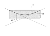
- XRD is performed on both outer peripheral ends of the wafer W, and a difference ⁇ between the measured X-ray diffraction peak angles between the two points is obtained. That is, the difference ⁇ between the X-ray diffraction peak angles at both outer peripheral ends of the wafer W is obtained. As shown in FIG. 10, this ⁇ is the difference between the measured inclinations of the atomic arrangement surface 22 at two points (ie, the inclinations of the tangents). As described above, an appropriate plane is selected according to the cut plane as the diffraction plane used for the X-ray diffraction measurement.
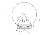
- FIG. 11 shows circles C that are in contact with two measured atomic arrangement planes, assuming that the curved surface of the atomic arrangement plane 22 of the wafer W is a part of a circle. It can be seen from FIG. 11 that the center angle ⁇ of the sector including the arc having the contact at both ends is equal to the difference ⁇ between the measured X-ray diffraction peak angles.
- the radius of curvature of the atomic arrangement surface 22 corresponds to the radius R of the arc.
- the radius R of the arc is obtained by the following relational expression.
- the amount of curvature d of the atomic arrangement surface 22 is obtained from the radius R of the arc and the radius r of the wafer W.
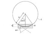
- the amount of curvature d of the atomic arrangement surface 22 corresponds to the radius R of the arc minus the distance of the perpendicular from the center of the arc down to the surface of the wafer W.
- the distance of the perpendicular from the center of the arc to the surface of the wafer W is calculated from the three-square theorem, and the following equation holds.
- the curvature d when the radius of curvature is positive (concave surface) is defined as a positive value
- the curvature d when the radius of curvature is negative (convex) is defined as a negative value.
- the X-ray diffraction peak angle may be measured at a plurality of locations, and the curvature per unit length may be converted from the following equation. For example, to improve the accuracy, it is preferable to measure the X-ray diffraction peak angle at five or more points including the center, the end, and the midpoint between the center and the end, and it is more preferable to perform the measurement at nine or more points.
- FIG. 13 shows an example in which the radius of curvature of the atomic arrangement surface is determined from a plurality of XRD measurement points.
- the horizontal axis in FIG. 13 is the relative position from the wafer center, and the vertical axis is the relative diffraction peak angle of each measurement point with respect to the wafer center diffraction peak angle.
- FIG. 14 schematically shows a cross section cut along a measurement direction of the atomic arrangement plane, for example, along the [1-100] direction, passing through the center in plan view.
- FIG. 9 illustrates an example in which the shape of the lattice array surface 22 is concavely curved.
- the diffraction peaks of the X-ray diffraction are measured at two points (two points indicated by a circle in FIG. 14) at a distance x from the center of the wafer W and the center of the wafer W. .
- the shape of the wafer W can be made approximately symmetrical as an approximation, and it can be estimated that the atomic arrangement plane 22 becomes flat at the center of the wafer W in plan view. Therefore, assuming that the difference between the inclinations of the atomic arrangement plane 22 at two points measured as specifically shown in FIG.
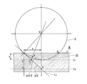
- FIG. 12B shows a supplementary diagram for deriving ⁇ / 2 in FIG. 12A. Points P, Q, S, T, U, V, and V in FIGS. 12A and 12B indicate the same position.
- a circle C is a circle that is in contact with the atomic arrangement surface on the assumption that the curved surface of the atomic arrangement surface 22 is a part of the circle, as in FIG.
- R be the radius of the circle C.
- Point O indicates the center of circle C.
- Tangent of the straight line L P is the point P
- the tangent of the straight line L T is the point T
- linear L T ' is the point V, which is a straight line parallel to the straight line L T.
- Point H indicates the midpoint of line segment PT. The intersection of the straight line and the tangent line L T passing through the point O and the point H and Z.
- the atomic arrangement plane at the wafer center and the measurement point at each point 22 relative atomic positions can be determined.
- the relative positions of the atoms on the atomic arrangement plane are obtained at each measurement point. Therefore, the amount of curvature (y 0 , y 1 , y 2 ) of the local atomic arrangement plane can be obtained.
- the relative atomic positions of the atomic arrangement plane 22 in the entire wafer W can be shown as a graph, which is useful for intuitively grasping the arrangement of the atomic arrangement planes 22, 22a, and 22b.
- the thickness of the sample for measuring the amount of curvature of the atomic arrangement surface 2 is preferably 500 ⁇ m or more, more preferably 750 ⁇ m or more, and further preferably 1 mm or more. If the thickness of the sample is 500 ⁇ m or more, the warpage of the sample can be suppressed. If the sample warps itself, it becomes difficult to accurately estimate the amount of curvature of the atomic arrangement surface 2.
- the amount of warpage of the sample is preferably 5 ⁇ m or less in any direction, more preferably 3 ⁇ m or less.
- the amount of warpage of the sample is defined as the maximum distance of a perpendicular that is lowered from the mounting surface, which is the flat surface side, of the sample surface toward the flat surface when the sample is mounted on the external flat surface. Indicates a value. That is, a predetermined surface of the SiC single crystal 1 is set as a mounting surface, and an external flat surface is set as a flat surface. When the SiC single crystal 1 is mounted such that the mounting surface is in contact with the flat surface, the maximum value of the distance between the mounting surface and the flat surface is referred to as the amount of warpage.
- the curved state of the atomic arrangement surface 2 functions as one index of quality.
- the curved state of the atomic arrangement plane includes a first direction passing through the center in plan view along the ⁇ 1-100> direction and a second direction perpendicular to the first direction passing through the center of the SiC single crystal in plan view along the ⁇ 11-20> direction. Evaluation is made in at least two directions, namely, two directions.
- the bending state of the atomic arrangement surface 2 is evaluated from the bending direction of the atomic arrangement surface 2 measured along each direction or the difference between the maximum value and the minimum value of the amount of bending (FIG. 4, step S3).
- the bending direction in each direction can be obtained by the method described above.
- the atomic arrangement surface 2 in the embodiment shown in FIG. 7 has a concave shape that is depressed toward the side opposite to the crystal growth direction in both the first direction and the second direction, and has the same curved direction.
- the atomic arrangement surface 2 in the embodiment shown in FIG. 8 has a convex shape protruding in the first direction in the crystal growth direction, and a concave shape depressed in the opposite direction to the crystal growth direction in the second direction. It is. That is, the bending directions are different in the two directions.
- the SiC ingot has been manufactured. That is, based on the result, the cutting condition of the SiC wafer or the growth condition of the next SiC ingot can be set. If the SiC ingot can be manufactured under appropriate conditions, the next manufacturing conditions are made similar to the current manufacturing conditions.
- the conditions for cutting the SiC wafer may be adjusted so as to increase the number of acquired high-quality SiC wafers, or may be adjusted so as to increase the number of acquired high-quality seed crystals.
- the curved state of the atomic arrangement plane in at least six directions rotated by 30 ° with respect to the first direction.
- the crystal structure of SiC single crystal 1 is hexagonal. Therefore, it can be determined that if the bending directions of the cut surfaces cut along the six directions symmetric with respect to the center are the same, a high-quality SiC wafer that hardly generates distortion and hardly generates BPD can be obtained. More preferably, measurement is performed in twelve directions rotated by 15 ° with respect to the first direction, and the evaluation is made based on a difference between a maximum value and a minimum value of the amount of bending in the twelve directions.
- the amount of curvature d1 of the atomic arrangement surface 2 measured along the first direction (see FIG. 5) and the amount of atomic arrangement surface measured along the second direction
- the determination is made based on the magnitude of the difference (
- the amount of bending in each direction can be obtained by the above-described method.
- FIG. 16A, FIG. 16B, and FIG. 16C are diagrams showing a relationship between BPD densities included in a crystal growth portion when a single crystal is grown on a predetermined SiC single crystal.
- FIG. 16A is a diagram showing a relationship between the absolute value of the amount of curvature d1 of the atomic arrangement surface 2 measured along the first direction passing through the center in plan view and the BPD density included in the crystal growth portion.
- the horizontal axis in FIG. 16A is the absolute value of the amount of curvature d1 of the atomic arrangement plane 2 in the cut plane cut along the [1-100] direction, and the vertical axis is the BPD density included in the crystal growth portion.
- FIG. 16A is the absolute value of the amount of curvature d1 of the atomic arrangement plane 2 in the cut plane cut along the [1-100] direction
- the vertical axis is the BPD density included in the crystal growth portion.
- FIG. 16B is a diagram illustrating a relationship between the absolute value of the amount of curvature d2 of the atomic arrangement surface 2 measured in the second direction and the density of BPD included in the crystal growth portion.
- the horizontal axis of FIG. 16B is the absolute value of the amount of curvature d2 of the atomic arrangement plane 2 in the cut plane cut along the [11-20] direction, and the vertical axis is the BPD density included in the crystal growth portion.
- FIG. 16C is a diagram showing relative values of the amount of curvature d1 and the amount of curvature d2, and the density of BPD contained in the crystal growth portion.
- the horizontal axis in FIG. 16C is the relative value of the amount of bending d1 and the amount of bending d2, and the vertical axis is the BPD density included in the crystal growth portion.
- SiSiC single crystals showing the relationship between the BPD densities contained in the crystal growth portions in FIGS. 16A, 16B and 16C were produced by a sublimation method.
- the diameter of the seed crystal was 16 cm.
- a SiC single crystal was grown by about 20 mm.
- BPD density was determined using KOH etching.
- the density of BPD can be reduced by using a SiC single crystal in which the difference between the amount of curvature d1 and the amount of curvature d2 is within a predetermined range. That is, when the difference between the amount of curvature d1 and the amount of curvature d2 is small, it can be determined that the SiC ingot is manufactured under appropriate conditions where BPD is unlikely to occur.
- a small value of the relative value between the bending amount d1 and the bending amount d2 means that the shape of the atomic arrangement surface 2 does not have anisotropy in a predetermined direction.
- the atomic arrangement surface 2 has a shape that is greatly bent in a predetermined direction.
- stress concentration tends to occur in that direction. The stress concentration induces the slip of the crystal plane, and may cause BPD.
- the bending amount d1 shows a negative value and the bending amount d2 shows a positive value. Therefore, for example, if the bending amount d1 is - ⁇ and the bending amount d2 is ⁇ using positive numbers ⁇ and ⁇ , the absolute value of the difference is ⁇ + ⁇ , and the difference between the bending amount d1 and the bending amount d2 is inevitable. Become larger.
- the SiC wafer Cutting conditions or growth conditions for the next SiC ingot can be set.
- the bending state of the atomic arrangement plane is measured in at least six directions rotated by 30 ° with respect to the first direction, and the maximum value of the bending amount in the six directions is measured. It is preferable to evaluate the difference between the minimum values.
- the crystal structure of SiC single crystal 1 is hexagonal. Therefore, if the amount of curvature of the atomic arrangement plane measured along six directions symmetrical with respect to the center in plan view is small, the atomic arrangement plane 2 is less likely to have anisotropy and high quality SiC which is less likely to generate BPD.
- a wafer is obtained. More preferably, measurement is performed in twelve directions rotated by 15 ° with respect to the first direction, and the evaluation is made based on a difference between a maximum value and a minimum value of the amount of bending in the twelve directions.
- the shape of the atomic arrangement surface 2 is evaluated by the head 6A or the tail 6B of the SiC ingot 6.
- the evaluation result of the head 6A or the tail 6B is not significantly different from the evaluation result inside the SiC ingot. Therefore, the quality of the obtained SiC ingot can be sufficiently evaluated based on the evaluation result of the head 6A or the tail 6B.
- FIG. 17 shows the results of measuring the shapes of the atomic arrangement planes of the head 6A and the tail 6B of the SiC ingot.
- the total growth amount of this ingot was 28 mm, and the tail 6B and the head 6A were located at positions where the growth amounts were 4 mm and 24 mm, respectively.
- the horizontal axis represents the angle between [11-20] when the counterclockwise direction is defined as positive and the measurement direction, and the vertical axis represents the amount of lattice bending. That is, 90 ° and ⁇ 90 ° in this drawing represent the same [1-100] direction.
- the most concave direction in the head 6A is a direction forming 30 ° with respect to [11-20], the amount of bending is 25.0 ⁇ m, and the most convex direction is [11-20].
- the amount of bending is ⁇ 2.5 ⁇ m.
- the most concave direction in the tail 6B is a direction of 30 ° with respect to [11-20], the amount of curvature is 21.4 ⁇ m, and the most convex direction is with respect to [11-20].
- the amount of bending is -2.5 ⁇ m.
- the cut surface cut by a wire saw or the like can be evaluated as it is, and polishing of the measurement surface is unnecessary.
- the evaluation can be performed at an arbitrary position cut out in a normal cutting step, it is not necessary to add a new processing step in implementing the present invention.
- the atomic arrangement plane can be easily measured by X-ray diffraction (XRD), it can be confirmed in about several hours. That is, if the method for evaluating a SiC single crystal according to the present embodiment is used, it is possible to easily determine whether the SiC ingot is good or bad. In other words, if the method for evaluating a SiC single crystal according to the present embodiment is used, the quality of a SiC ingot can be easily evaluated. Further, the evaluation result can be promptly fed back to the next SiC ingot manufacturing condition and the SiC wafer slicing method, and the time required for manufacturing the SiC wafer can be greatly reduced.
- FIG. 18 is a diagram schematically showing a conventional method for evaluating the quality of a SiC ingot.
- the conventional SiC ingot first obtains an evaluation wafer (step S11), and processes it so that the evaluation wafer can be used for evaluation (step S12). Thereafter, the presence or absence of stacking faults and dislocation concentrated portions is confirmed by an X-ray topograph (Step S13), and the number of defects is counted by KOH etching (Step S14). Then, based on the obtained results, the next SiC ingot manufacturing condition and the SiC wafer slicing method are determined.
- Evaluation wafer processing, KOH etching, and counting the number of defects are time-consuming, and require several weeks to several months to confirm quality. That is, it takes time to feed back the next SiC ingot manufacturing conditions and the SiC wafer slicing method, and the overall time required to manufacture the SiC wafer increases. The next ingot can be manufactured without waiting for the feedback of the quality evaluation.However, if there is an abnormality in the quality due to deviation of the manufacturing conditions, etc. Since no abnormality can be detected, adjustment of manufacturing conditions and the like cannot be performed. As a result, there is a risk that a defective ingot may be continuously produced during that time, which is not preferable.
- the quality of the SiC single crystal can be easily measured by using the SiC single crystal evaluation method according to the present embodiment.
- the curved state of the atomic arrangement surface functions as an index of BPD generation, and a SiC single crystal in which BPD is unlikely to be generated can be easily determined.
Landscapes
- Chemical & Material Sciences (AREA)
- Crystallography & Structural Chemistry (AREA)
- General Physics & Mathematics (AREA)
- Health & Medical Sciences (AREA)
- Life Sciences & Earth Sciences (AREA)
- Analytical Chemistry (AREA)
- Biochemistry (AREA)
- General Health & Medical Sciences (AREA)
- Physics & Mathematics (AREA)
- Immunology (AREA)
- Pathology (AREA)
- Inorganic Chemistry (AREA)
- Engineering & Computer Science (AREA)
- Materials Engineering (AREA)
- Metallurgy (AREA)
- Organic Chemistry (AREA)
- Crystals, And After-Treatments Of Crystals (AREA)
- Physical Deposition Of Substances That Are Components Of Semiconductor Devices (AREA)
- Analysing Materials By The Use Of Radiation (AREA)
Abstract
このSiC単結晶の評価方法は、SiC単結晶の平面視中心を通り<1-100>方向に沿う第1方向と、前記第1方向と垂直で前記SiC単結晶の平面視中心を通り<11-20>方向に沿う第2の方向と、の少なくとも二方向における原子配列面の湾曲状態を評価する。
Description
本発明は、SiC単結晶の評価方法及びSiCウェハの製造方法に関する。
本願は、2018年8月13日に日本国に出願された特願2018-152317号に基づき優先権を主張し、その内容をここに援用する。
本願は、2018年8月13日に日本国に出願された特願2018-152317号に基づき優先権を主張し、その内容をここに援用する。
炭化珪素(SiC)は、シリコン(Si)に比べて絶縁破壊電界が1桁大きく、バンドギャップが3倍大きい。また、炭化珪素(SiC)は、シリコン(Si)に比べて熱伝導率が3倍程度高い等の特性を有する。炭化珪素(SiC)は、パワーデバイス、高周波デバイス、高温動作デバイス等への応用が期待されている。
半導体等のデバイスには、SiCウェハ上にエピタキシャル膜を形成したSiCエピタキシャルウェハが用いられる。SiCウェハ上に化学的気相成長法(Chemical
Vapor Deposition:CVD)によって設けられたエピタキシャル膜が、SiC半導体デバイスの活性領域となる。
Vapor Deposition:CVD)によって設けられたエピタキシャル膜が、SiC半導体デバイスの活性領域となる。
そのため、割れ等の破損が無く、欠陥の少ない、高品質なSiCウェハが求められている。なお、本明細書において、SiCエピタキシャルウェハはエピタキシャル膜を形成後のウェハを意味する。本明細書において、SiCウェハはエピタキシャル膜を形成前のウェハを意味する。
例えば、特許文献1には、ウェハの反り量及び結晶方位のズレ量を所定の範囲内にすることで、SiCウェハ上に形成されるエピタキシャル膜が良好となることが記載されている。
また特許文献2には、ウェハ面内の成長面方位のずれを所定の範囲内とすることで、良質なエピタキシャル膜が得られることが記載されている。
また高品質なSiCウェハを得るために、各工程において品質の評価が行われている。例えば、SiCインゴットの品質は、評価用ウェハを切断加工した後に、X線トポグラフ解析(XRT)、KOHエッチング等を用いて評価する(特許文献3)。SiCインゴットの品質を充分評価してから取得するSiCウェハ枚数及び種結晶数を決定すると、SiC単結晶のロス量を低減できる。
しかしながら、特許文献3に記載の方法では、SiCインゴットを評価用ウェハに加工し、エッチング等で品質を評価するのに時間がかかる。その結果、SiCインゴットからSiCウェハを加工するまでの間に、数週間単位の時間的なロスが生じる。
また特許文献1及び特許文献2に記載のSiCウェハのように、所定の方向における格子ズレの程度を制御したのみでは、基底面転位(BPD)の発生を充分に抑制することができない場合がある。基底面転位(BPD)は、SiCウェハのキラー欠陥の一つであり、基底面において生じるすべりが発生の原因の一つであると考えられている欠陥である。
本発明は上記問題に鑑みてなされたものであり、高品質なSiC単結晶ウェハを効率的に提供することを目的とする。
本発明者らは、鋭意検討の結果、SiC単結晶の原子配列面(格子面)の湾曲状態を少なくとも二方向で評価することで、基底面転位(BPD)を発生しにくいSiC単結晶を簡便に評価できることを見出した。
またSiC単結晶の原子配列面を簡便に評価することで、SiCインゴットの大まかな品質を把握でき、SiCインゴットの切断条件及び次回の単結晶の成長条件を素早くフィードバックできることを見出した。
すなわち、本発明は、上記課題を解決するために、以下の手段を提供する。
またSiC単結晶の原子配列面を簡便に評価することで、SiCインゴットの大まかな品質を把握でき、SiCインゴットの切断条件及び次回の単結晶の成長条件を素早くフィードバックできることを見出した。
すなわち、本発明は、上記課題を解決するために、以下の手段を提供する。
(1)第1の態様にかかるSiC単結晶の評価方法は、SiC単結晶の平面視中心を通り<1-100>方向に沿う第1方向と、前記第1方向に垂直で前記SiC単結晶の平面視中心を通り<11-20>方向に沿う第2方向と、の少なくとも二方向における原子配列面の湾曲状態を評価する。
(2)上記態様にかかるSiC単結晶の評価方法において、前記原子配列面の湾曲状態を、前記第1方向を基準に30°ずつ回した少なくとも六方向で評価してもよい。
(3)上記態様にかかるSiC単結晶の評価方法において、前記原子配列面の湾曲状態を、測定方向における前記原子配列面の湾曲方向が一致するか否かにより評価してもよい。
(4)上記態様にかかるSiC単結晶の評価方法において、前記原子配列面の湾曲状態を、測定方向における前記原子配列面の湾曲量の最大値及び最小値の差から評価してもよい。
(5)上記態様にかかるSiC単結晶の評価方法において、前記原子配列面の湾曲状態をX線回折により評価してもよい。
(6)上記態様にかかるSiC単結晶の評価方法において、前記SiC単結晶の平面視中心を通る同一方向における5箇所以上の点に対してX線回折を行い、前記原子配列面の湾曲状態を評価してもよい。
(6)上記態様にかかるSiC単結晶の評価方法において、前記SiC単結晶の平面視中心を通る同一方向における5箇所以上の点に対してX線回折を行い、前記原子配列面の湾曲状態を評価してもよい。
(7)第2の態様にかかるSiC単結晶の製造方法は、上記態様にかかるSiC単結晶の評価方法による評価結果に基づき、SiCインゴットのスライス方法又はSiC単結晶の成長条件を決定する。
上記態様にかかるSiC単結晶の評価方法を用いると、高品質なSiC単結晶ウェハを効率的に提供できる。
以下、本実施形態の好ましい例について、図を適宜参照しながら詳細に説明する。以下の説明で用いる図面は、便宜上特徴となる部分を拡大して示している場合があり、各構成要素の寸法比率などは実際とは異なっていることがある。以下の説明において例示される材質、寸法等は一例であって、本発明はそれらに限定されるものではなく、その要旨を変更しない範囲で適宜変更して実施することが可能である。また以下の例は、発明の趣旨をより良く理解させるために具体的に好ましい例を説明するものであり、特に指定のない限り、本発明を限定するものではない。本発明の趣旨を逸脱しない範囲で、長さ、位置、形状、数、量、及び料等について、省略、追加、置換、その他の変更が可能である。
図1は、本実施形態にかかるSiCウェハの製造方法を模式的に示した図である。図1に示すように、まず種結晶を準備する。そして種結晶上に、SiCを結晶成長させSiCインゴットを作製する。得られたSiCインゴットは品質評価を受け、SiCウェハに加工され、出荷される。またSiCインゴットの一部は、次のSiCインゴット作製のための種結晶に加工される。作製されたSiCウェハは、種々の加工がされる場合がある。例えば、SiCウェハの表面にエピタキシャル膜を形成されるとSiCエピタキシャルウェハになる。また、SiCエピタキシャルウェハは、エピタキシャル膜の一部を加工されるとSiCデバイスになる。
図2は、SiCインゴットを作製する際に用いられる製造装置の一例の断面模式図である。図2に示す製造装置100は、昇華法を利用したSiC単結晶の製造装置の一つである。昇華法は、原料を加熱することによって生じた原料ガスを単結晶(種結晶)上で再結晶化し、大きな単結晶(インゴット)を得る方法である。
図2に示す製造装置100は、坩堝10とコイル20とを有する。坩堝10とコイル20との間には、コイル20の誘導加熱により発熱する発熱体(図視略)を有してもよい。
坩堝10は、原料Gと対向する位置に設けられた結晶設置部11を有する。坩堝10は、内部に結晶設置部11から原料Gに向けて拡径するテーパーガイド12を有してもよい。図2では、理解を容易にするために、原料G、種結晶5及び種結晶から成長したSiCインゴット6を同時に図示している。
コイル20に交流電流を印加すると、坩堝10が加熱され、原料Gから原料ガスが生じる。発生した原料ガスは、テーパーガイド12に沿って結晶設置部11に設置された種結晶5に供給される。種結晶5に原料ガスが供給されることで、種結晶5の主面にSiCインゴット6が結晶成長する。種結晶5の結晶成長面は、カーボン面(C面)、又は、カーボン面から0~10°以下のオフ角を設けた面とすることが好ましい。種結晶5の結晶成長面は、カーボン面、又は、カーボン面から0~5°のオフ角を設けた面であることがより好ましい。
図3は、種結晶5上に結晶成長したSiCインゴット6の一例の断面模式図である。SiCインゴットは、一般にマルチワイヤーソー等切断工程に投入する前にはSiCインゴット6の結晶成長面近傍(以下、ヘッド6Aと言う)や種結晶5近傍(以下、テール6Bと言う)を予め切除する工程が必要である。
図4は、本実施形態にかかるSiCインゴットの品質評価方法を模式的に示した図である。図4に示すようにまずSiCインゴットのテール又はヘッドを切断し、取得する(工程S1)。上述のように、マルチワイヤーソー等による切断には予めヘッド6A又はテール6B等を取得する工程が必要である。そのため当該評価方法を用いることで新たに追加の切断工程が発生したり、製品取得部を犠牲にして評価サンプルを取得したりする必要はない。
次いで、ヘッド6A又はテール6Bにおける原子配列面の湾曲状態を評価する(図4、工程S2)。まず、原子配列面について説明する。図5は、平面視中心を通る[1-100]方向に延在する直線に沿って、ヘッド6A又はテール6Bを構成するSiC単結晶を切断した切断面の一例の模式図である。また図6は、平面視中心を通る[11-20]方向に延在する直線に沿って、ヘッド6A又はテール6Bを構成するSiC単結晶を切断した切断面の一例の模式図である。図5及び図6において上側が[000-1]方向、すなわち<0001>方向に垂直に切断をした時にカーボン面(C面、(000-1)面)が現れる方向である。以下、第1方向と第2方向とが、それぞれ[1-100]方向と[11-20]方向との場合を例に説明する。図5および図6は、いずれもSiC単結晶の一部分を示すものである。
本明細書において、「平面視中心」とは、評価対象であるSiC単結晶が平面視で円形であるもの、一部が欠けているが、その欠けている部分を仮想的に補うと円形になるもの(例えば、オリフラを有するSiCウェハ)である場合には、その円形の中心を意味する。しかし、この場合に限定されない。例えば、SiC単結晶のインゴットは公知の方法(例えば、昇華法)によって結晶成長させた場合、結晶成長方向に垂直な断面は円形であるから、結晶成長方向に垂直な断面で切断されたウェハあるいは切断体の場合は平面視円形であるから、この場合も「平面視中心」とは、その円形の中心を意味する。一方、SiC単結晶のインゴットを結晶成長方向に交差する方向(垂直方向を除く)で切断されたウェハあるいは切断体の場合は平面視楕円形であるから、この場合「平面視中心」とは、その楕円形の長軸と短軸の交点を意味する。
本明細書において、「平面視中心」とは、評価対象であるSiC単結晶が平面視で円形であるもの、一部が欠けているが、その欠けている部分を仮想的に補うと円形になるもの(例えば、オリフラを有するSiCウェハ)である場合には、その円形の中心を意味する。しかし、この場合に限定されない。例えば、SiC単結晶のインゴットは公知の方法(例えば、昇華法)によって結晶成長させた場合、結晶成長方向に垂直な断面は円形であるから、結晶成長方向に垂直な断面で切断されたウェハあるいは切断体の場合は平面視円形であるから、この場合も「平面視中心」とは、その円形の中心を意味する。一方、SiC単結晶のインゴットを結晶成長方向に交差する方向(垂直方向を除く)で切断されたウェハあるいは切断体の場合は平面視楕円形であるから、この場合「平面視中心」とは、その楕円形の長軸と短軸の交点を意味する。
ここで結晶方位及び原子配列面(格子面、結晶格子面)は、ミラー指数として以下の括弧を用いて表記される。()と{}は面を表す時に用いられる(特に面指数とも言われる)。()は特定の面を表現する際に用いられ、{}は結晶の対称性による等価な面の総称(集合面)を表現する際に用いられる。一方で、<>と[]は方向を表す時に用いられる(特に方向指数とも言われる)。[]は特定の方向を表現する際に用いられ、<>は結晶の対称性による等価な方向を表現する際に用いられる。面指数と同じ指数で表記された方向指数は、その面の法線の方向を示す。
図5及び図6に示すように、ヘッド6A又はテール6Bを構成するSiC単結晶1は、複数の原子Aが整列してなる単結晶である。そのため図5及び図6に示すように、SiC単結晶の切断面をミクロに見ると、複数の原子Aが配列した原子配列面2が形成されている。切断面における原子配列面2は、切断面に沿って配列する原子Aを繋いで得られる切断方向と略平行な方向に延在する線として表記される。
切断面における原子配列面2の形状は、SiC単結晶1の最表面の形状によらず、凸形状、凹形状となっている場合がある。また原子配列面2の形状は切断方向によって異なっている場合がある。原子配列面2の形状としては、例えば図7に示すような形状や図8に示すような形状等がある。図7に示すような形状は、平面視中心に向かって窪んだ凹形状である。図8に示すような形状は、所定の切断面では凹形状、異なる切断面では凸形状のポテトチップス型(鞍型)の形状である。すなわち、原子配列面2の形状には、任意の切断方向で同じ形状のものと、切断方向により形状が異なるものとがある。
原子配列面2の湾曲量はX線回折(XRD)により測定できる。言い換えると、原子配列面2の形状はX線回折(XRD)に基づいて決定できる。測定する面は測定する方向に応じて決定される。測定方向を[hkil]とすると、測定面は(mh mk mi n)の関係を満たす必要がある。ここで、mは0以上の整数であり、nは自然数である。例えば、[11-20]方向に測定する場合は、m=0、n=4として(0004)面、m=2、n=16として(22-416)面等が選択される。一方で、[1-100]方向に測定する場合は、m=0、n=4として(0004)面、m=3、n=16として(3-3016)面等が選択される。すなわち測定面は、測定方向によって異なる面であってもよく、原子配列面は必ずしも同じ面とはならなくてもよい。上記関係を満たすことで、結晶成長時に及ぼす影響の少ないa面又はm面方向の格子湾曲をc面方向の格子湾曲と誤認することを防ぐことができる。また測定はC面、Si面のいずれの面を選択してもよいが、一つのサンプルにおいて測定方向は変更しない。ここで原子配列面2の湾曲量は、SiC単結晶1の平面視中心における原子位置と、SiC単結晶1の端部における[000-1]方向の原子位置との差を意味する。原子配列面2が平面視中心に向かって窪んだ凹形状の場合の湾曲量を正とし、平面視中心に向かって突出した凸形状の場合の湾曲量を負とする。
X線回折データは例えば、所定の方向に沿って中心、端部を2点、中心と端部との中点を2点、の計5点において取得することが好ましい。原子配列面2が湾曲している場合、X線の反射方向が変わるため、中心とそれ以外の部分とで出力されるX線回折像のピークのω角の位置が変動する。この回折ピークの位置変動から原子配列面2の湾曲方向を求めることができる。また回折ピークの位置変動から原子配列面2の曲率半径も求めることができ、原子配列面2の湾曲量も求めることができる。
尚、X線回折データを取得する数および位置は、上記の例のみに限定されない。例えば、X線回折データを、ウェハWの中心を通る同一直線上の7点で取得しても良いし、9点取得してもよい。X線回折データを5点で取得する場合、精度向上のため上記の位置で取得することが好ましい。例えば、所定の方向に沿って、「中心、端部、中心と端部との中点」のそれぞれの中点でX線回折データを取得することが好ましい。
尚、X線回折データを取得する数および位置は、上記の例のみに限定されない。例えば、X線回折データを、ウェハWの中心を通る同一直線上の7点で取得しても良いし、9点取得してもよい。X線回折データを5点で取得する場合、精度向上のため上記の位置で取得することが好ましい。例えば、所定の方向に沿って、「中心、端部、中心と端部との中点」のそれぞれの中点でX線回折データを取得することが好ましい。
(原子配列面の湾曲方向及び湾曲量の測定方法(方法1)の具体的な説明)
平面視で円形である円柱状のSiC単結晶(インゴット)の一部を結晶成長方向に対して垂直にスライスした円板状の試料(以下、ウェハWと言う)の外周端部分のXRDの測定値から原子配列面の湾曲方向及び湾曲量を測定する方法について具体的に説明する。
平面視で円形である円柱状のSiC単結晶(インゴット)の一部を結晶成長方向に対して垂直にスライスした円板状の試料(以下、ウェハWと言う)の外周端部分のXRDの測定値から原子配列面の湾曲方向及び湾曲量を測定する方法について具体的に説明する。
図9は、ウェハWの断面模式図である。図9に平面視中心を通り原子配列面の測定の方向、例えば[1-100]方向に沿って切断した切断面を模式的に示す。ウェハWの半径をrとすると、断面の横方向の長さは2rとなる。また図9にウェハWにおける原子配列面22の形状も図示している。図9に示すように、ウェハW自体の形状は平坦であるが、原子配列面22は湾曲している場合がある。図9に示す原子配列面22は左右対称であり、凹型に湾曲している。この対称性は、インゴットの製造条件が通常中心軸(平面視で円の中心を通り、結晶成長方向に延びる軸)に対して対称性があることに起因する。なお、この対称性とは、完全対称である必要はなく、製造条件の揺らぎ等に起因したブレを容認する近似としての対称性を意味する。
XRDをウェハWの両外周端部に対して行い、測定した2点間のX線回折ピーク角度の差Δθを求める。すなわち、ウェハWの両外周端部におけるX線回折ピーク角度の差Δθを求める。図10に示すように、このΔθが測定した2点の原子配列面22の傾き(すなわち、接線の傾き)の差になっている。X線回折測定に用いる回折面は、上述のように切断面にあわせて適切な面を選択する。
次に、図11を参照して、得られたΔθから湾曲した原子配列面22の曲率半径を求める方法を説明する。図11には、ウェハWの原子配列面22の曲面が円の一部であると仮定して、測定した2箇所の原子配列面に接する円Cを示している。図11から幾何学的に、接点を両端とする円弧を含む扇型の中心角φは、測定したX線回折ピーク角度の差Δθと等しくなることがわかる。原子配列面22の曲率半径は、当該円弧の半径Rに対応する。円弧の半径Rは以下の関係式で求められる。

そして、この円弧の半径RとウェハWの半径rとから、原子配列面22の湾曲量dが求められる。図12に示すように、原子配列面22の湾曲量dは、円弧の半径Rから、円弧の中心からウェハWの表面に下した垂線の距離を引いたものに対応する。円弧の中心からウェハWの表面に下した垂線の距離は、三平方の定理から算出され、以下の式が成り立つ。なお、本明細書では曲率半径が正(凹面)の場合の湾曲量dを正の値とし、負(凸面)の場合の湾曲量dを負の値と定義する。

上述のように、XRDのウェハWの両外側端部の測定値だけからRを測定することもできる。一方で、この方法を用いると、測定箇所に局所的な歪等が存在した場合において、必ずしも形状を見誤る可能性がないとはいえない。その為、複数箇所でX線回折ピーク角度の測定を行って、単位長さ辺りの曲率を以下の式から換算してもよい。例えば、精度の向上のため中心、端部、中心と端部との中点を含む5箇所以上でX線回折ピーク角度の測定を行うことが好ましく9箇所以上で測定を行うことがより好ましい。

図13に、複数のXRDの測定点から原子配列面の曲率半径を求めた例を示す。図13の横軸はウェハ中心からの相対位置であり、縦軸はウェハ中心回折ピーク角に対する各測定点の相対的な回折ピーク角度を示す。図13は、ウェハの[1-100]方向を測定し、測定面を(3-3016)とした例である。測定箇所は5カ所で行った。5点はほぼ直線に並んでおり、この傾きから、dθ/dr=8.69×10-4deg/mmが求められる。この結果を上式に適用することでR=66mの凹面であることが計算できる。そして、このRとウェハの半径r(75mm)から、原子配列面の湾曲量dが42.6μmと求まる。
ここまで原子配列面の形状が凹面である例で説明したが、凸面の場合も同様に求められる。凸面の場合は、Rはマイナスとして算出される。
(原子配列面の湾曲方向及び湾曲量の別の測定方法(方法2)の説明)
原子配列面の湾曲方向及び湾曲量は、別の方法で求めてもよい。図14に平面視中心を通り原子配列面の測定の方向、例えば[1-100]方向に沿って切断した切断面を模式的に示す。図9では、格子配列面22の形状が凹状に湾曲している場合を例に説明する。
原子配列面の湾曲方向及び湾曲量は、別の方法で求めてもよい。図14に平面視中心を通り原子配列面の測定の方向、例えば[1-100]方向に沿って切断した切断面を模式的に示す。図9では、格子配列面22の形状が凹状に湾曲している場合を例に説明する。
図14に示すように、ウェハWの中心とウェハWの中心から距離xだけ離れた場所の2箇所(図14中で○印で示した2箇所)で、X線回折の回折ピークを測定する。インゴットの製造条件の対称性からウェハWの形状は、近似として左右対称とすることができ、原子配列面22はウェハWの平面視中心で平坦になると推定できる。そのため、図15Aに具体的に示すように測定した2点における原子配列面22の傾きの差をΔθとすると、ウェハWの中心における接線と、ウェハWの中心と原子配列面22上においてウェハWの中心から距離xだけれた場所とを結ぶ直線との傾きの差は(Δθ/2)である。従って、ウェハWの平面視中心を基準として距離xだけ離れた場所における原子配列面22の相対的な位置yは以下の式で表記できる。図12Bに、図12AにおけるΔθ/2を導出するための補足図を示す。図12A及び図12B中の点P、Q、S、T、U、V、Vは同じ位置を示す。図12Bにおいて、円Cは、図6と同様に、原子配列面22の曲面が円の一部であると仮定して原子配列面に接する円である。円Cの半径をRとする。点Oは円Cの中心を示す。直線LPは点Pの接線、直線LTは点Tの接線、直線LT’は点Vを通り、直線LTに平行な直線である。点Hは線分PTの中点を示す。点Oと点Hを通る直線と接線LTとの交点をZとする。△PZHと△TZHとは、線分PH=線分TH、線分ZHは共通、∠PHZ=∠THZ=90°であるから、合同である。従って、∠HPZ=∠HTZである。また、錯角の関係により∠HPQ=∠HTZである。∠PZS=Δθであり、錯角の関係により∠PZS=∠QPZ=∠HPZ+∠HPQ=2∠HTZであるから、∠HTZ=Δθ/2が得られる。∠HTZ=∠PTSであり、y/x=tan∠PTSであるから、以下の式が得られる。

図14Cに示すように、中心からの距離xの位置を変えて(x0、x1、x2)複数箇所の測定をすることで、それぞれの点でウェハ中心と測定点とにおける原子配列面22の相対的な原子位置を求めることができる。
この方法は、それぞれの測定箇所で原子配列面における原子の相対位置が求められる。そのため、局所的な原子配列面の湾曲量(y0、y1、y2)を求めることができる。また、ウェハW全体において原子配列面22の相対的な原子位置をグラフとして示すことができ、原子配列面22、22a、22bのならびを感覚的に把握するために有益である。
この方法は、それぞれの測定箇所で原子配列面における原子の相対位置が求められる。そのため、局所的な原子配列面の湾曲量(y0、y1、y2)を求めることができる。また、ウェハW全体において原子配列面22の相対的な原子位置をグラフとして示すことができ、原子配列面22、22a、22bのならびを感覚的に把握するために有益である。
一方で、それぞれの点における測定は、それぞれ1か所での測定値に基づくものであるため、回折条件によっては部分的に測定しにくい位置(特にウェハの一方の端部近く)が生じる場合があり、また結晶性が悪い部分があると誤差を含みやすい場合がある。その為、現状の測定技術では、この方法は原子配列面22の反りの大きさを測定する方法として用いるよりも、原子配列面の並びを感覚的に把握するための参考値を得る際に用いることが好ましい。
原子配列面2の湾曲量を測定する試料の厚みは、500μm以上であることが好ましく、750μm以上であることがより好ましく、1mm以上であることがさらに好ましい。試料の厚みが500μm以上であれば、試料の反りを抑制できる。試料自体が反ると、原子配列面2の湾曲量を正確に見積もることが難しくなる。試料の反り量としては、任意の方向に5μm以下であることが好ましく、3μm以下であることがより好ましい。ここで試料の反り量とは、外部の平坦面に試料を載置した際に、試料の面のうち平坦面側の面である載置面から平坦面に向けて下した垂線の距離の最大値を指す。すなわち、SiC単結晶1の所定の面を載置面とし、外部の平坦な面を平坦面とする。載置面が平坦面と接触するにようにSiC単結晶1を載置したとき、載置面と平坦面との距離の最大値を反り量という。
原子配列面2の湾曲状態は、品質の一つの指標として機能する。原子配列面の湾曲状態は、平面視中心を通り<1-100>方向に沿う第1方向と、第1方向と垂直でSiC単結晶の平面視中心を通り<11-20>方向に沿う第2の方向との少なくとも二方向で評価する。
原子配列面2の湾曲状態は、それぞれの方向に沿って測定した原子配列面2の湾曲方向、又は、湾曲量の最大値と最小値との差から評価する(図4、工程S3)。
原子配列面2の湾曲方向から評価する場合は、第1方向に沿って測定した原子配列面2の湾曲方向と、第2方向に沿って測定した原子配列面2の湾曲方向とが一致するか否かを判断する。各方向における湾曲方向は上述の方法で求めることができる。例えば、図7に示す態様における原子配列面2は、第1方向及び第2方向のいずれにおいても結晶成長方向と反対側に向かって窪む凹形状であり、湾曲方向は一致している。これに対し、図8に示す態様における原子配列面2は、第1方向は結晶成長方向に向かって突出する凸形状であり、第2方向は結晶成長方向と反対側に向かって窪む凹形状である。すなわち、二つの方向で湾曲方向は異なっている。
第1方向及び第2方向の原子配列面2の湾曲方向が同一の場合、そのSiC単結晶を種結晶として結晶成長を行った結晶成長部分内におけるBPD密度は低くなる。この理由は明確ではないが、原子配列面2が二つの方向で異なる方向に湾曲すると、原子配列面2が歪む(図8参照)。原子配列面2が歪むと、温度変化が生じた際に複数の方向に応力が発生し、原子配列面2にひずみが生じやすくなる。原子配列面2のひずみは、結晶面の滑りを誘起し、BPDの原因となりうると考えられる。上記事項は、第1方向及び第2方向の原子配列面がいずれも凹形状である場合、第1方向及び第2方向の原子配列面がいずれも凸形状である場合、のいずれの場合においても当てはまる。
すなわち、第1方向に沿って測定した原子配列面2の湾曲方向と、第2方向に沿って測定した原子配列面2の湾曲方向とが一致する場合は、BPDが発生しにくい適切な条件でSiCインゴットが作製されていると判断できる。つまり、この結果に基づき、SiCウェハの切断条件、又は、次回のSiCインゴットの成長条件を設定できる。適切な条件でSiCインゴットを作製できている場合は、次回の製造条件を現在の製造条件と類似させる。またSiCウェハの切断条件は、SiCウェハの高品質なウェハの取得枚数を増やすように調整してもよいし、高品質な種結晶の取得枚数を増やすように調整してもよい。
またより高品質なSiCウェハが求められている場合は、原子配列面の湾曲状態を、第1方向を基準に30°ずつ回した少なくとも六方向で評価することが好ましい。SiC単結晶1の結晶構造は六方晶である。そのため、中心に対して対称な六方向に沿って切断した切断面における湾曲方向が同一であればよりひずみが生じにくく、BPDの発生しにくい高品質なSiCウェハを得ることができることを判断できる。また、第1方向を基準に15°ずつ回した十二方向で測定し、十二方向における湾曲量の最大値と最小値の差で評価することがより好ましい。
一方で、原子配列面2の湾曲量から評価する場合は、第1方向に沿って測定した原子配列面2の湾曲量d1(図5参照)と、第2方向に沿って測定した原子配列面2の湾曲量d2(図6参照)との差の大きさ(|d2-d1|)で判断する。各方向における湾曲量は上述の方法で求めることができる。
図16A、図16Bおよび図16Cは、所定のSiC単結晶上に単結晶を結晶成長した際に、結晶成長部分内に含まれるBPD密度の関係を示した図である。図16Aは、平面視中心を通り第1方向に沿って測定した原子配列面2の湾曲量d1の絶対値と、結晶成長部分内に含まれるBPD密度との関係を示した図である。図16Aの横軸は、[1-100]方向に沿って切断した切断面における原子配列面2の湾曲量d1の絶対値であり、縦軸は結晶成長部分内に含まれるBPD密度である。図16Bは、第2方向に沿って測定した原子配列面2の湾曲量d2の絶対値と、結晶成長部分内に含まれるBPDの密度との関係を示した図である。図16Bの横軸は、[11-20]方向に沿って切断した切断面における原子配列面2の湾曲量d2の絶対値であり、縦軸は結晶成長部分内に含まれるBPD密度である。図16Cは湾曲量d1と湾曲量d2の相対値と、結晶成長部分内に含まれるBPDの密度を示した図である。図16Cの横軸は、湾曲量d1と湾曲量d2の相対値であり、縦軸は結晶成長部分内に含まれるBPD密度である。
図16A、図16Bおよび図16Cに結晶成長部分内に含まれるBPD密度の関係を示すSiC単結晶は、昇華法により作製した。種結晶の直径は16cmであった。種結晶上には、SiC単結晶を約20mm結晶成長させた。BPD密度は、KOHエッチングを用いて求めた。
図16A及び図16Bに示すように、湾曲量d1、d2とBPDとの間には相関が確認されない。そのため、湾曲量d1、d2の絶対値が小さいSiC単結晶を用いた場合に、BPDの発生頻度が必ず低下するわけではない。すなわち湾曲量d1、d2の絶対値は、BPDの密度の指標としては十分に機能していない。
これに対し図16Cに示すように、湾曲量d1と湾曲量d2の相対値と、BPDとの間には相関がみられる。湾曲量d1と湾曲量d2の相対値が大きくなると、BPDの発生頻度が高まる傾向にある。換言すると、湾曲量d1と湾曲量d2との差が所定の範囲内であるSiC単結晶を用いると、BPDの密度を低減できる。すなわち、湾曲量d1と湾曲量d2の差が小さい場合は、BPDが発生しにくい適切な条件でSiCインゴットが作製されていると判断できる。
湾曲量d1と湾曲量d2との相対値と、BPDの密度の間に上述の関係が見られるのは、以下の理由が考えられる。湾曲量d1と湾曲量d2との相対値の値が小さいということは、原子配列面2の形状が所定の方向に異方性を有していないことを意味する。例えば、第1方向の湾曲量d1と第2方向の湾曲量d2との差が大きい場合、原子配列面2は所定の方向に大きく曲がった形状となる。原子配列面2の形状が所定の方向に大きな異方性を有すると、温度変化が生じた際にその方向に応力集中が生じやすくなる。応力集中は、結晶面の滑りを誘起し、BPDの原因となりうる。
なお、図8に示すように原子配列面2の湾曲方向が第1方向と第2方向とで異なるポテトチップス型の場合、湾曲量d1は負の値、湾曲量d2は正の値を示す。そのため例えば、正の数α、βを用いて、湾曲量d1を-α、湾曲量d2をβとすると、これらの差分の絶対値はα+βとなり、湾曲量d1と湾曲量d2との差は必然的に大きくなる。
上述のように、第1方向に沿って測定した原子配列面2の湾曲量d1と、第2方向に沿って測定した原子配列面2の湾曲量d2との差の結果に基づき、SiCウェハの切断条件、又は、次回のSiCインゴットの成長条件を設定できる。
またより高品質なSiCウェハが求められている場合は、原子配列面の湾曲状態を、第1方向を基準に30°ずつ回した少なくとも六方向で測定し、六方向における湾曲量の最大値と最小値の差で評価することが好ましい。SiC単結晶1の結晶構造は六方晶である。そのため、平面視中心に対して対称な六方向に沿って測定した原子配列面の湾曲量が小さければ、より原子配列面2は異方性を有し難く、BPDの発生しにくい高品質なSiCウェハが得られる。また、第1方向を基準に15°ずつ回した十二方向で測定し、十二方向における湾曲量の最大値と最小値の差で評価することがより好ましい。
ここで原子配列面2の形状は、SiCインゴット6のヘッド6A又はテール6Bで評価している。ヘッド6A又はテール6Bの評価結果は、SiCインゴットの内部の評価結果と大きく違わない。そのため、ヘッド6A又はテール6Bの評価結果を基に、得られたSiCインゴットの品質を充分評価できる。
図17は、SiCインゴットのヘッド6A、テール6Bの原子配列面の形状を測定した結果である。このインゴットの総成長量は28mmであり、テール6B、ヘッド6Aはそれぞれ成長量が4mm、24mmの位置であった。横軸は反時計回りを正としたときの[11-20]と測定方向とのなす角、縦軸は格子湾曲量を表している。すなわちこの図における90°と-90°は同じ[1-100]方向を表している。
またヘッド6Aにおいて最も凹となっている方向は[11-20]に対して30°をなす方向で、湾曲量は25.0μmであり、最も凸になっている方向は[11-20]に対して-60°をなす方向で、湾曲量は-2.5μmである。テール6Bにおいて最も凹となっている方向は[11-20]に対して30°の方向で、湾曲量は21.4μmであり、最も凸になっている方向は[11-20]に対して-60°をなす方向で、湾曲量は-2.5μmである。すなわち、成長初期にあたるテール部から成長後期にあたるヘッド部に至るまで、SiCインゴット内で原子配列面2の形状及び湾曲量に大きな差はないと言える。したがって、作製されたSiCインゴットの結晶成長方向における任意の1箇所の格子湾曲量を測定することでSiCインゴット全体の格子湾曲を把握することが可能である。
この評価はワイヤーソー等により切り出された切断面をそのまま評価することが可能であり、測定面の研磨は不要である。また評価は通常の切断工程で切り出される任意の箇所で実施可能であるため、本発明を実施する上で新たに加工工程が加える必要はない。また原子配列面もX線回折(XRD)で簡便に測定できるため、数時間程度の時間で確認できる。すなわち、本実施形態にかかるSiC単結晶の評価方法を用いれば、SiCインゴットの良、不良を簡便に判定できる。換言すると、本実施形態にかかるSiC単結晶の評価方法を用いれば、SiCインゴットの品質を簡便に評価することができる。またこの評価結果を次回のSiCインゴットの作製条件、SiCウェハのスライス方法に迅速にフィードバックを行うことができ、SiCウェハの製造にかかる時間を大幅に短縮できる。
ここで図18は、従来のSiCインゴットの品質評価方法を模式的に示した図である。図18に示すように従来のSiCインゴットは、まず評価用ウェハを取得し(工程S11)、評価用ウェハで評価を行えるように加工する(工程S12)。その後、X線トポグラフ(工程S13)により積層欠陥や転位集中部の有無を確認し、KOHエッチングにより欠陥数をカウントする(工程S14)。そして得られた結果に基づき、次回のSiCインゴットの作製条件、SiCウェハのスライス方法を決定する。
評価用ウェハの加工やKOHエッチングの作業及び欠陥数をカウントする作業は時間がかかり、品質の確認に数週間から数か月の時間が必要である。すなわち、次回のSiCインゴットの作製条件、SiCウェハのスライス方法のフィードバックに時間がかかり、SiCウェハの製造にかかる全体の時間が長くなる。品質評価のフィードバックを待たずに次回のインゴット作製を行うこともできるが、作製条件のズレ等で品質に異常があった場合、インゴット外観に異常が見られなければ品質評価結果が判明するまでは異常を検知できないため作製条件の調整等を行うことができない。結果としてその間に不良のインゴットが作製され続けてしまう危険性があるため好ましくない。
上述のように、本実施形態にかかるSiC単結晶の評価方法を用いると、SiC単結晶の品質を簡便に測定できる。また原子配列面の湾曲状態は、BPDの発生の指標として機能し、BPDが発生しにくいSiC単結晶を容易に判別できる。
以上、本発明の好ましい実施の形態について詳述したが、本発明は特定の実施の形態に限定されるものではなく、特許請求の範囲内に記載された本発明の要旨の範囲内において、種々の変形・変更が可能である。
1…SiC単結晶、2…原子配列面、5…種結晶、6…SiCインゴット、6A…ヘッド、6B…テール、10…坩堝、11…結晶設置部、12…テーパーガイド、20…コイル、100…製造装置、A…原子、G…原料
Claims (7)
- SiC単結晶の平面視中心を通り<1-100>方向に沿う第1方向と、前記第1方向と垂直で前記SiC単結晶の平面視中心を通り<11-20>方向に沿う第2方向と、の少なくとも二方向における原子配列面の湾曲状態を評価する、SiC単結晶の評価方法。
- 前記原子配列面の湾曲状態を、前記第1方向を基準に30°ずつ回した少なくとも六方向で評価する、請求項1に記載のSiC単結晶の評価方法。
- 前記原子配列面の湾曲状態を、測定方向における前記原子配列面の湾曲方向が一致するか否かにより評価する、請求項1又は2のいずれかに記載のSiC単結晶の評価方法。
- 前記原子配列面の湾曲状態を、測定方向における前記原子配列面の湾曲量の最大値及び最小値の差から評価する、請求項1~3のいずれか一項に記載のSiC単結晶の評価方法。
- 前記原子配列面の湾曲状態をX線回折により評価する、請求項1~4のいずれか一項に記載のSiC単結晶の評価方法。
- 前記X線回折により前記SiC単結晶の平面視中心と、端部と、中心と端部との中点と、の5点においてX線回折を行い、原子配列面の一方向における原子配列面の湾曲状態を評価する、請求項5に記載のSiC単結晶の評価方法。
- 請求項1~6のいずれか一項に記載のSiC単結晶の評価方法による評価結果に基づき、SiCインゴットのスライス方法又は次回のSiC単結晶の成長条件を決定する、SiCウェハの製造方法。
Applications Claiming Priority (2)
| Application Number | Priority Date | Filing Date | Title |
|---|---|---|---|
| JP2018-152317 | 2018-08-13 | ||
| JP2018152317A JP7117938B2 (ja) | 2018-08-13 | 2018-08-13 | SiC単結晶の評価方法及びSiCウェハの製造方法 |
Publications (1)
| Publication Number | Publication Date |
|---|---|
| WO2020036166A1 true WO2020036166A1 (ja) | 2020-02-20 |
Family
ID=69525333
Family Applications (1)
| Application Number | Title | Priority Date | Filing Date |
|---|---|---|---|
| PCT/JP2019/031799 Ceased WO2020036166A1 (ja) | 2018-08-13 | 2019-08-13 | SiC単結晶の評価方法及びSiCウェハの製造方法 |
Country Status (2)
| Country | Link |
|---|---|
| JP (1) | JP7117938B2 (ja) |
| WO (1) | WO2020036166A1 (ja) |
Cited By (2)
| Publication number | Priority date | Publication date | Assignee | Title |
|---|---|---|---|---|
| JP2023011328A (ja) * | 2021-07-12 | 2023-01-24 | 住友重機械工業株式会社 | アニール評価装置、アニール装置、アニール評価方法、及びアニール方法 |
| TWI811746B (zh) * | 2020-07-27 | 2023-08-11 | 環球晶圓股份有限公司 | 碳化矽晶種及其製造方法、碳化矽晶體的製造方法 |
Citations (4)
| Publication number | Priority date | Publication date | Assignee | Title |
|---|---|---|---|---|
| JPS6373104A (ja) * | 1986-09-17 | 1988-04-02 | Toshiba Corp | 格子彎曲測定用x線回折装置 |
| WO2009035095A1 (ja) * | 2007-09-12 | 2009-03-19 | Showa Denko K.K. | エピタキシャルSiC単結晶基板及びエピタキシャルSiC単結晶基板の製造方法 |
| JP2011111372A (ja) * | 2009-11-27 | 2011-06-09 | Showa Denko Kk | 炭化珪素単結晶及びその製造方法、並びに炭化珪素単結晶ウェーハ及び炭化珪素単結晶インゴット |
| JP2013136494A (ja) * | 2011-12-28 | 2013-07-11 | Toyota Central R&D Labs Inc | 単結晶製造装置、SiC単結晶、ウェハ、及び、半導体デバイス |
-
2018
- 2018-08-13 JP JP2018152317A patent/JP7117938B2/ja active Active
-
2019
- 2019-08-13 WO PCT/JP2019/031799 patent/WO2020036166A1/ja not_active Ceased
Patent Citations (4)
| Publication number | Priority date | Publication date | Assignee | Title |
|---|---|---|---|---|
| JPS6373104A (ja) * | 1986-09-17 | 1988-04-02 | Toshiba Corp | 格子彎曲測定用x線回折装置 |
| WO2009035095A1 (ja) * | 2007-09-12 | 2009-03-19 | Showa Denko K.K. | エピタキシャルSiC単結晶基板及びエピタキシャルSiC単結晶基板の製造方法 |
| JP2011111372A (ja) * | 2009-11-27 | 2011-06-09 | Showa Denko Kk | 炭化珪素単結晶及びその製造方法、並びに炭化珪素単結晶ウェーハ及び炭化珪素単結晶インゴット |
| JP2013136494A (ja) * | 2011-12-28 | 2013-07-11 | Toyota Central R&D Labs Inc | 単結晶製造装置、SiC単結晶、ウェハ、及び、半導体デバイス |
Cited By (4)
| Publication number | Priority date | Publication date | Assignee | Title |
|---|---|---|---|---|
| TWI811746B (zh) * | 2020-07-27 | 2023-08-11 | 環球晶圓股份有限公司 | 碳化矽晶種及其製造方法、碳化矽晶體的製造方法 |
| US11781241B2 (en) | 2020-07-27 | 2023-10-10 | Globalwafers Co., Ltd. | Silicon carbide seed crystal and method of manufacturing the same, and method of manufacturing silicon carbide ingot |
| JP2023011328A (ja) * | 2021-07-12 | 2023-01-24 | 住友重機械工業株式会社 | アニール評価装置、アニール装置、アニール評価方法、及びアニール方法 |
| JP7719648B2 (ja) | 2021-07-12 | 2025-08-06 | 住友重機械工業株式会社 | アニール評価装置、アニール装置、アニール評価方法、及びアニール方法 |
Also Published As
| Publication number | Publication date |
|---|---|
| JP2020026372A (ja) | 2020-02-20 |
| JP7117938B2 (ja) | 2022-08-15 |
Similar Documents
| Publication | Publication Date | Title |
|---|---|---|
| US11905621B2 (en) | SiC single crystal, method of manufacturing SiC ingot, and method of manufacturing SiC wafer | |
| JP5273741B2 (ja) | エピタキシャルSiC単結晶基板及びエピタキシャルSiC単結晶基板の製造方法 | |
| US11466383B2 (en) | Silicon carbide ingot, method of preparing the same, and method for preparing silicon carbide wafer | |
| US10837123B2 (en) | Method of manufacturing SiC ingot | |
| JP6916835B2 (ja) | 面取り炭化ケイ素基板および面取り方法 | |
| JP7571902B2 (ja) | SiC単結晶、SiC種結晶及びSiCインゴットの製造方法 | |
| US10844517B2 (en) | Method of processing SiC single crystal and method of manufacturing SiC ingot | |
| JP7117938B2 (ja) | SiC単結晶の評価方法及びSiCウェハの製造方法 | |
| US20230268177A1 (en) | SiC EPITAXIAL WAFER AND METHOD FOR MANUFACTURING SAME | |
| JP6722578B2 (ja) | SiCウェハの製造方法 | |
| WO2020036167A1 (ja) | SiC単結晶の貼合方法、SiCインゴットの製造方法及びSiC単結晶成長用台座 | |
| WO2020036163A1 (ja) | SiC単結晶の評価方法、及び品質検査方法 | |
| US20210189596A1 (en) | SiC SINGLE CRYSTAL, METHOD OF MANUFACTURING SiC INGOT, AND METHOD OF MANUFACTURING SiC WAFER | |
| US20260110112A1 (en) | N-type gan substrate and n-type gan crystal | |
| US20250263868A1 (en) | Gallium nitride single crystal substrate and method for producing the same | |
| WO2025205614A1 (ja) | GaN基板、GaN結晶の製造方法およびGaN基板の製造方法 |
Legal Events
| Date | Code | Title | Description |
|---|---|---|---|
| 121 | Ep: the epo has been informed by wipo that ep was designated in this application |
Ref document number: 19849377 Country of ref document: EP Kind code of ref document: A1 |
|
| NENP | Non-entry into the national phase |
Ref country code: DE |
|
| 122 | Ep: pct application non-entry in european phase |
Ref document number: 19849377 Country of ref document: EP Kind code of ref document: A1 |