WO2020031364A1 - Antenna device - Google Patents
Antenna device Download PDFInfo
- Publication number
- WO2020031364A1 WO2020031364A1 PCT/JP2018/030022 JP2018030022W WO2020031364A1 WO 2020031364 A1 WO2020031364 A1 WO 2020031364A1 JP 2018030022 W JP2018030022 W JP 2018030022W WO 2020031364 A1 WO2020031364 A1 WO 2020031364A1
- Authority
- WO
- WIPO (PCT)
- Prior art keywords
- plate
- antenna device
- tuning
- antenna element
- antenna
- Prior art date
Links
Images


Classifications
-
- H—ELECTRICITY
- H01—ELECTRIC ELEMENTS
- H01Q—ANTENNAS, i.e. RADIO AERIALS
- H01Q5/00—Arrangements for simultaneous operation of antennas on two or more different wavebands, e.g. dual-band or multi-band arrangements
- H01Q5/20—Arrangements for simultaneous operation of antennas on two or more different wavebands, e.g. dual-band or multi-band arrangements characterised by the operating wavebands
- H01Q5/25—Ultra-wideband [UWB] systems, e.g. multiple resonance systems; Pulse systems
-
- G—PHYSICS
- G01—MEASURING; TESTING
- G01R—MEASURING ELECTRIC VARIABLES; MEASURING MAGNETIC VARIABLES
- G01R29/00—Arrangements for measuring or indicating electric quantities not covered by groups G01R19/00 - G01R27/00
- G01R29/08—Measuring electromagnetic field characteristics
- G01R29/0864—Measuring electromagnetic field characteristics characterised by constructional or functional features
- G01R29/0878—Sensors; antennas; probes; detectors
-
- H—ELECTRICITY
- H01—ELECTRIC ELEMENTS
- H01Q—ANTENNAS, i.e. RADIO AERIALS
- H01Q1/00—Details of, or arrangements associated with, antennas
- H01Q1/48—Earthing means; Earth screens; Counterpoises
-
- H—ELECTRICITY
- H01—ELECTRIC ELEMENTS
- H01Q—ANTENNAS, i.e. RADIO AERIALS
- H01Q17/00—Devices for absorbing waves radiated from an antenna; Combinations of such devices with active antenna elements or systems
- H01Q17/001—Devices for absorbing waves radiated from an antenna; Combinations of such devices with active antenna elements or systems for modifying the directional characteristic of an aerial
-
- H—ELECTRICITY
- H01—ELECTRIC ELEMENTS
- H01Q—ANTENNAS, i.e. RADIO AERIALS
- H01Q5/00—Arrangements for simultaneous operation of antennas on two or more different wavebands, e.g. dual-band or multi-band arrangements
- H01Q5/50—Feeding or matching arrangements for broad-band or multi-band operation
Definitions
- the present invention relates to an antenna device, and particularly, performs communication with another wireless device at a frequency of 600 MHz to 6 GHz (commonly called sub 6) used in fifth generation mobile communication, and performs a communication test on the other wireless device.
- the present invention relates to an antenna device capable of performing such operations.
- Patent Literature 1 discloses a flat base antenna having a substantially home-base shape that is symmetrical with respect to a horizontal line in a plan view, and a substantially flat rectangular ground that is disposed on the same substrate surface as the antenna and capacitively coupled to the antenna.
- a UWB antenna device provided is described.
- the band where the VSWR (Voltage Standing Wave Ratio) is 2.0 or less is 3.1 GHz to 5 GHz, and the antenna device is used in mobile phones and smartphones.
- VSWR Voltage Standing Wave Ratio
- the present invention has been made in view of the above circumstances, and a single antenna device continuously matches the entire frequency band of 600 MHz to 6 GHz, so that a plurality of types of antennas having different frequency bands can be used without switching the antenna device. It is an object of the present invention to provide an antenna device capable of communicating with another communication device.
- the present invention provides an antenna element including an arc peripheral part at least in a part of a peripheral part, and a power supply unit in a part of the arc peripheral part, and a back side of the antenna element.
- a tuning plate having a thin plate-shaped conductor longer than the maximum diameter of the antenna element, and a region facing the back surface of the antenna element being a capacitive coupling portion;
- a radio wave absorber arranged on the back side of the capacitive coupling portion of the tuning plate to absorb radio waves radiated from the back side of the antenna element; and a radio wave absorber through the side surface of the radio wave absorber.
- a surplus portion of the tuning plate that is folded back to the back side, and a metal plating film is formed on the front surface and disposed on the back side of the radio wave absorber, and provided on the surplus length portion of the tuning plate.
- a tuning plated plate connecting the over scan portion electrically characterized in that it and a grounding member connected to said tuning plating plate and electrically.
- one antenna device continuously matches the entire frequency band of 600 MHz to 6 GHz, thereby enabling communication with a plurality of types of communication devices using different frequency bands without switching the antenna device. It is possible to provide an antenna device that performs
- FIG. 2 is an exploded perspective view of the antenna device according to the first embodiment of the present invention. It is a perspective view showing the section which cut the antenna device along the signal input member.
- FIG. 4 is a perspective view showing a cross section of the antenna device cut by a surface along a signal input member and a surface orthogonal to the surface. It is the perspective view which observed the antenna element assembled in the antenna device from the back side.
- (A), (b) is a perspective view showing the appearance of the antenna device according to the second embodiment of the present invention. It is an exploded perspective view of the antenna device concerning a second embodiment of the present invention.
- FIG. 9 is a flowchart showing a calibration procedure of the measurement system shown in FIG. More specifically, it shows a calibration procedure of the measurement system, which is performed prior to the measurement of the return loss characteristic and the coupling characteristic of the antenna device.
- 9 is a flowchart illustrating a return loss measuring procedure performed in the measurement system illustrated in FIG. 8.
- 9 is a flowchart showing a procedure for measuring coupling loss characteristics performed in the measurement system shown in FIG. 8.
- FIG. 4 is a graph showing standard characteristics of return loss when the first antenna device configured in the first embodiment is a normal model.
- FIG. 11 is a graph illustrating standard characteristics of return loss when the first antenna device configured in the second embodiment is an NFC model.
- FIG. 9 is a graph showing comparative characteristics representing the effect of the tuning plate of the first antenna device. It is a graph which shows the comparative characteristic showing the effect by the tuning plating plate of a 1st antenna device.
- FIGS. 1A and 1B are perspective views showing the appearance of an antenna device according to a first embodiment of the present invention.
- FIG. 2 is an exploded perspective view of the antenna device according to the first embodiment of the present invention.
- FIG. 3 is a perspective view showing a cross section of the antenna device cut along the signal input member.
- FIG. 4 is a perspective view showing a cross section of the antenna device cut by a surface along the signal input member and a surface orthogonal to the surface.
- the antenna device according to the present embodiment is characterized in that an insulator is inserted between the antenna element and the tuning plate.
- the side from which the electromagnetic wave is radiated is referred to as the upper side (upper surface) or the front side (front surface), and the opposite side is referred to as the lower side (lower surface) or the back side (back surface).
- the extending direction of the coaxial connector is referred to as a depth direction, and a direction perpendicular to the vertical direction and the depth direction is referred to as a width direction.
- the antenna device 1 includes a case 10 that forms a hollow housing portion that houses each constituent member.
- the case 10 includes a substantially rectangular base 11 and an upper cover 12 fixed to the base 11 with screws.
- One side plate 13 extending in the width direction of the upper cover 12 has a coaxial member insertion hole 14 through which the signal input member 61 of the coaxial connector 60 is inserted, and an insertion hole for fixing the coaxial connector 60 to the side plate 13 with screws. 15 are formed through.
- a semi-disc-shaped (or bow-shaped) antenna element 30 is accommodated inside the case 10.
- a first insulating plate 40 that insulates the antenna element 30 from other members, a tuning plate 45 that functions as a short stub, and a radio wave absorber having a predetermined thickness t
- the body 50 and the tuning plating plate 55 are sequentially laminated.
- Reference numeral 16 in the figure is an element guide for positioning the antenna element 30 in the case 10.
- FIG. 5 is a perspective view of the antenna element assembled to the antenna device as viewed from the back side.
- the antenna element 30 has a shape obtained by removing a smaller bow-shaped portion from two bow-shaped portions formed by cutting a copper plate into two with a single chord 31 from a circular copper plate.
- the antenna element 30 includes an arc peripheral edge portion 32 at least at a part of the peripheral edge portion, and includes a feeder 33 at a part of the arc peripheral edge portion 32.
- the antenna element 30 includes a chord 31 that connects between the end points of the circular arc peripheral part 32 at the other part of the peripheral part.
- the length of the string 31 is about 59 mm.
- the central angle of the antenna element 30 (the central angle with respect to the arc peripheral portion 32) is larger than 180 degrees and is about 245 degrees.
- the antenna element 30 has a feeding portion 33 at an appropriate position on the circular arc peripheral portion 32, more specifically, at the center of the circular arc peripheral portion 32.
- the size of the antenna element 30 was determined in consideration of the effect of shortening the wavelength due to the dielectric constant of the radio wave absorber. Assuming that the radio wave absorber is polyurethane, when a wavelength shortening coefficient of 0.45 when the dielectric constant is 5 is reflected in ⁇ / 4 of 600 MHz, the shortened wavelength becomes 56 mm. Therefore, a circle having a diameter of 56 mm was used as an initial shape. From the results of experiments in which the diameter was gradually increased from this circle, the final diameter of the circle was 70 mm.
- chord 31 the bow-shaped portion is removed to form a straight edge (chord 31).
- the size of the chord 31 is approximately ⁇ / 4 of 600 MHz, and the size that reflects the shortening factor is determined from experiments. Since the characteristics were the best, the string 31 had a size of about 59 mm.
- the first insulating plate 40 is made of an insulating synthetic resin such as an acrylic plate or a PVC plate.
- the first insulating plate 40 plays a role of insulating the antenna element 30 and the radio wave absorber 50.
- the first insulating plate 40 is set to have such a size that the antenna element 30 and the tuning plate 45 are not electrically connected to each other and can reliably maintain an insulating state.
- the tuning plate 45 functions as a stub (short stub) for performing impedance matching by capacitively coupling with the antenna element 30 according to the area facing the antenna element 30.
- the tuning plate 45 is opposed to the back side of the antenna element 30 in an insulated state.
- the tuning plate 45 is formed of a thin plate-shaped conductor longer than the maximum diameter (maximum width) of the antenna element 30. More specifically, the tuning plate 45 has a substantially strip shape and is made of a brass foil (brass foil, conductor) having a length in the longitudinal direction of 115 mm, a length in the width direction of 25 mm, and a thickness of 0.05 mm.
- a region facing the back surface of the antenna element 30 via the first insulating plate 40 is a capacitive coupling portion 45a.
- the extra length portions (45b, 45c) of the tuning plate 45 are folded back to the back surface side of the radio wave absorber 50 via the side surface portions of the radio wave absorber 50.
- a ground portion 45 b that is electrically connected to the tuning plating plate 55 is provided in a surplus portion that is folded back on the back surface side of the radio wave absorber 50.
- the ground portion 45b faces the back surface of the radio wave absorber 50.
- a connecting portion 45c that connects the capacitive coupling portion 45a and the ground portion 45b is provided between the capacitive coupling portion 45a and the ground portion 45b.
- the tuning plate 45 is curved and deformed into a J-shape or a U-shape, or bent into a square U-shape, so that the capacitive coupling portion 45a and the ground portion 45b are connected to the front side and the back side of the radio wave absorber 50. , And the radio wave absorber 50 is sandwiched in the thickness direction.
- the capacitive coupling portion 45a faces the back surface of the antenna element 30 via the first insulating plate 40, and the ground portion 45b provided at the other end in the longitudinal direction directly faces the surface of the tuning plating plate 55. .
- the capacitive coupling portion 45a is capacitively coupled to the antenna element 30.
- the amount of capacitive coupling (tuning frequency or resonance frequency) between the tuning plate 45 and the antenna element 30 can be adjusted.
- the capacitive coupling portion 45a faces the antenna element 30 over the entire area in the width direction of the antenna element 30.
- the longitudinal length of the capacitive coupling portion 45a is set to have a length substantially equal to or longer than the diameter of the antenna element 30. Accordingly, the amount of capacitive coupling with the antenna element 30 is adjusted by the length in the short direction of the capacitive coupling portion 45a (the length in the depth direction of the antenna device 1).
- an impedance chart (see FIG. 17) is used. Impedance matching is performed on a 50 ⁇ coaxial cable according to a known matching strategy method.
- the tuning frequency of the tuning plate 45 according to the present embodiment is set to 1.3 GHz to 4.5 GHz
- the longitudinal length of the tuning plate 45 is 115 mm
- the longitudinal length of the capacitive coupling portion 45a is 74 mm
- the width direction length is It can be set as 25 mm.
- the radio wave absorber 50 is disposed on the back side of the capacitive coupling portion 45a of the tuning plate 45.
- the radio wave absorber 50 absorbs and attenuates radio waves radiated from the back side of the antenna element 30.
- the radio wave absorber 50 is made of foamed polyurethane in which carbon powder is dispersed and foamed.
- the radio wave absorber 50 has a size (area) that covers the entire surface of the antenna element 30.
- the radio wave absorption characteristics of the radio wave absorber 50 are determined by its thickness t.
- the radio wave absorber 50 only needs to have a performance of absorbing radio waves in the entire frequency range to which the antenna device 1 can (match).
- the radio wave absorber 50 may be ECOSORB AN74 (thickness 19 mm, corresponding frequency 500 MHz to 9 GHz) manufactured by E & C Engineering Co., Ltd.
- the radio wave absorber 50 can reduce the return loss characteristic of the antenna device 1 over the entire frequency range (matchable) to which the antenna device 1 corresponds. Play a role to improve. Further, since the radio wave absorber 50 has a certain degree of elasticity, the radio wave absorber 50 is compressed in the up and down direction of the antenna device 1 at the time of assembling, thereby preventing displacement of each member assembled inside the case 10. Fulfill. For example, by compressing the radio wave absorber 50 made of a foam having a thickness of about 20 mm by about 2 mm and assembling it in the case 10, it is possible to effectively prevent misalignment of other members incorporated in the case 10. Can be.
- the tuning plating plate 55 is disposed on the back side of the radio wave absorber 50. A part of the upper surface of the tuning plating plate 55 is directly opposed to and contacts the rear surface of the radio wave absorber 50, and the other portion is one end in the longitudinal direction of a ground portion 45 b of the tuning plate 45 and a ground plate (ground member) 85 described later. It faces the back surface of the radio wave absorber 50 via the portion 85a.
- the tuning plating plate 55 is electrically connected to the ground portion 45b of the tuning plate 45 by making surface contact with the ground portion 45b, and is electrically connected by making surface contact with one end portion 85a of the ground plate 85 in the longitudinal direction.
- the tuning plating plate 55 a metal plating film is formed on the upper surface of a rectangular flat plate made of ABS resin which is a synthetic resin. This metal plating film is a vacuum nickel vapor deposition plating film.
- the tuning plating plate 55 has a square shape with one side of 48 mm and a thickness of 1 mm.
- the tuning plating plate 55 is capacitively coupled to the antenna element 30 via the tuning plate 45, and mainly serves to tune electromagnetic waves in a relatively low frequency band of 600 MHz to 1.5 GHz. From the results of experiments, it is sufficient for the tuning plating plate 55 to fulfill the above role if the tuning plating plate 55 is arranged so that 85% or more of its area is located immediately below the antenna element 30. Further, the tuning plating plate 55 plays a role of a shield for preventing radio wave leakage from the lower surface of the antenna device 1 to the outside.
- the antenna device 1 includes a coaxial connector 60 having a signal input member 61 in which a center conductor 64 is electrically and mechanically fixed to the feeding portion 33 of the antenna element 30, and a cloth-like conductor at least on an outer peripheral portion (outer surface).
- a grounding plate (grounding member) 85 that comes into contact with the grounding portion 45b.
- a second insulating plate 81 for insulating both is inserted.
- a slit 81a is formed in the vertical direction to allow the center conductor 64 of the signal input member 61 to pass from the side plate 13 toward the antenna element 30.
- the coaxial connector 60 includes a signal input member 61 disposed at one end in the axial direction, a flange 67 disposed at an intermediate portion in the axial direction and electrically connected to the outer conductor 62 of the signal input member 61, and a coaxial connector 60 disposed at the other end in the axial direction. And a connector portion (coaxial receptacle) 71 which is electrically connected to each conductor of the signal input member 61 and detachably connects the transmission cable.
- the signal input member 61 is a semi-rigid coaxial member, and is inserted into the case 10 through the coaxial member insertion hole 14.
- the outer conductor 62 of the signal input member 61 is formed of a seamless metal cylinder.
- a central conductor 64 is accommodated in the hollow portion of the outer conductor 62 via an insulator 63 such as a fluororesin or polyimide.
- the outer conductor 62 of the signal input member 61 is made of copper, and the center conductor 64 is a silver-plated copper-coated steel wire.
- One end portion 64a of the central conductor 64 in the axial direction projects outward beyond one end edge of the outer conductor 62 in the axial direction.
- the outer conductor 62 surrounds the center conductor 64 at the other end in the axial direction.
- One axial end portion 64 a of the central conductor 64 exposed to the outside is fixed to the power supply portion 33 provided on the back surface of the antenna element 30 by soldering.
- the axial direction of the signal input member 61 extends in the depth direction with respect to the antenna device 1.
- the signal input member 61 extends in the direction along the tangent line of the circular arc peripheral portion 32 with respect to the antenna element 30, that is, in the direction orthogonal to the chord 31. It is growing.
- An insertion hole 68 through which a shaft of a screw 77 is inserted is formed at an appropriate position of the flange 67.
- the flange 67 is fixed to the side plate 13 of the upper cover 12.
- a connector plate 73 having a screw hole 74 in which a thread is formed is attached to the inner surface of the side plate 13. Further, a cable insertion portion 75 for passing the signal input member 61 is formed at an appropriate position in the plane of the connector plate 73.
- the flange 67 and the connector plate 73 are made of a conductor such as iron.
- the coaxial connector 60 inserts the shaft portion of the screw 77 into each hole in a state where the screw hole 74 of the connector plate 73 communicates with the insertion holes 15 and 68 formed in the side plate 13 and the flange portion 67, respectively. Then, it is fixed to the side plate 13 of the upper cover 12 by being screwed into the screw hole 74. Since the connector plate 73 is electrically connected to the flange 67 via the conductive screw 77, the connector plate 73 is also electrically connected to the outer conductor 62 of the signal input member 61.
- the connector section 71 is an SMA (Sub Miniature Type A) type 50 ⁇ connector, and detachably connects a transmission cable that is a coaxial cable for transmitting a high-frequency signal.
- SMA Subscribe Miniature Type A
- the inner conductor of the transmission cable and the center conductor 64 of the signal input member 61 conduct, and the outer conductor of the transmission cable and the outer conductor 62 of the signal input member 61 conduct.
- the ground plate 85 is a means for improving VSWR (Voltage Standing Wave Ratio) characteristics in all frequency bands (600 MHz to 6 GHz) to which the antenna device 1 according to the present embodiment corresponds.
- the ground plate 85 has a substantially rectangular shape and is made of brass foil (brass foil) having a thickness of 0.05 mm.
- the length of the ground plate 85 in the width direction is 45 mm, which is the same as the length of the conductive cushion 80 in the width direction.
- the length (longitudinal length) of the ground plate 85 in the direction orthogonal to the width direction is such that the ground plate 85 can directly or indirectly ground the conductive cushion 80, the tuning plating plate 55, and the tuning plate 45. Is set to
- Part of the ground plate 85 (in this example, the middle portion in the longitudinal direction) is disposed between the inner surface of the side plate 13 and the connector plate 73, and is screwed to the connector plate 73 together with the side plate 13 and the flange 67 by screws 77. The position is fixed in the case 10 by being fastened together.
- the ground plate 85 is in close contact with the connector plate 73, so that the ground plate 85 is electrically connected to the outer conductor 62 of the signal input member 61 via the screw 77.
- the grounding plate 85 is bent or bent at an appropriate position in the longitudinal direction at the time of assembling, so that the grounding plate 85 has a posture in which it is roughly J-shaped, L-shaped, U-shaped, or square U-shaped in the case 10.
- one end portion 85a of the earth plate 85 in the longitudinal direction makes surface contact with the surface of the tuning plating plate 55 and an appropriate portion of the earth portion 45b of the tuning plate 45, and the other end portion 85b of the longitudinal direction contacts the conductive cushion 80.
- the other end 85b in the longitudinal direction is set to a length that does not protrude beyond the second insulating plate 81 toward the antenna element 30. That is, the ground plate 85 does not face the upper surface of the antenna element 30.
- the conductive cushion 80 (80a, 80b) is electrically connected to the outer conductor 62 by holding the outer conductor 62 of the signal input member 61 between the upper and lower directions.
- the conductive cushion 80 is pressed by the outer conductor 62 and deformed, thereby playing a role of stabilizing the vertical position of the signal input member 61 inside the antenna device 1.
- the conductive cushion 80 is formed by using a foam material that can be elastically deformed as a core material and integrating a conductive cloth material with the outer peripheral portion thereof.
- the foam is desirably made of an insulator such as foamed polyurethane, foamed chloroprene rubber, and rubber sponge.
- a conductive urethane worm or the like can be used for the foam.
- the conductive cloth material is, for example, a mesh-shaped conductor formed by weaving or knitting metal fibers, and can be formed, for example, from a metal wire obtained by plating nickel on copper. Note that the conductive cloth material may be a non
- the conductive cushion 80 is arranged so that its longitudinal direction extends in a direction intersecting with the axial direction of the signal input member 61 (a direction substantially orthogonal to the axis), that is, in a width direction of the antenna device 1.
- the tuning frequency of the conductive cushion 80 can be adjusted by the length of the conductive cushion 80 in the width direction of the antenna device 1.
- an impedance chart (see FIG. 17) was used. Impedance matching is performed on the 50 ⁇ coaxial cable according to a well-known matching strategy.
- the conductive cushion 80a disposed above the signal input member 61 can have a thickness (length in the vertical direction) of 4 mm ⁇ width (length in the depth direction) of 10 mm ⁇ length of 45 mm.
- the conductive cushion 80b disposed on the side can be 8 mm thick ⁇ 10 mm wide ⁇ 45 mm long.
- the tuning frequency of the conductive cushion 80 is 4.5 GHz to 6 GHz.
- the antenna device 1 has a wavelength (600 MHz to 6 GHz) corresponding to the (matchable) wavelength / 4 (125 mm to 12.5 mm) with respect to the wavelength in consideration of the wavelength shortening.
- a sufficiently large antenna element 30 was employed, and a member for improving return loss characteristics was attached according to each frequency band.
- the tuning plating plate 55 mainly improves return loss characteristics in the 600 MHz to 1.5 GHz band
- the tuning plate 45 mainly improves return loss characteristics in the 1.3 GHz to 4.5 GHz band.
- 80 mainly improves the return loss characteristic in the 4.5 to 6 GHz band.
- the radio wave absorber 50 improves the return loss characteristics in the 500 MHz to 9 GHz band.
- the member for improving the return loss characteristic according to each frequency band it is possible to perform radio wave measurement in a wide frequency band with one antenna device. Further, the matching is performed by utilizing the dielectric constant, whereby the wavelength is shortened, and the antenna device can be downsized.
- FIGS. 6A and 6B are perspective views showing the appearance of an antenna device according to a second embodiment of the present invention.
- FIG. 7 is an exploded perspective view of the antenna device according to the second embodiment of the present invention.
- the antenna device according to the present embodiment is characterized in that it has an NFC board that performs wireless communication based on NFC (Near Field Communication).
- NFC Near Field Communication
- the antenna device 2 includes an NFC board 90 disposed above (front side) the antenna element 30.
- the NFC board 90 is housed in the case 10 in a non-contact state with the antenna element 30 by being sandwiched between the element guide 16 and the upper surface plate 17 of the upper cover 12.
- the NFC board 90 is provided with a USB (Universal Serial Bus) terminal 91 as a connection terminal for wired communication at an appropriate position at the edge.
- the USB terminal 91 is exposed to the outside via a USB terminal hole 19 formed through an arbitrary side plate 18 of the upper cover 12.
- the NFC board 90 is a communication board that performs short-range wireless communication in a frequency band different from the frequency band radiated by the antenna element 30.
- the NFC board 90 is interposed between an information processing device such as a personal computer that can be connected to the USB terminal 91 and a wireless communication terminal that can perform communication by NFC.
- the wireless communication terminal is a device that transmits and receives information wirelessly, such as a mobile phone, a smartphone, and a Wi-Fi router, and uses any of the frequency bands (600 MHz to 6 GHz included in the antenna device 2) using the antenna device 2. (Frequency range).
- the information processing device when performing a communication test in each frequency band (any band within the range of 600 MHz to 6 GHz) using the antenna device 2, transmits a communication result from the wireless communication terminal by NFC. Acquisition and transmission of an instruction from the information processing apparatus to the wireless communication terminal to generate a radio wave according to the test content by NFC can be performed.
- FIG. 8A is a block diagram showing an antenna system and a measurement system using the antenna device according to one embodiment of the present invention
- FIG. 8B is a perspective view showing a calibration kit used for calibrating the measurement system. It is.
- the antenna system 300 illustrated in FIG. 8A includes a pair of antenna devices, each of which is referred to as a first antenna device 301 and a second antenna device 303. The signal is received by the second antenna device 303 which is arranged to face the radiation direction of one antenna device 301.
- the measurement system 310 includes a network analyzer 315 and a monitor 313, connects a coaxial cable 307 between a terminal P1 of the network analyzer 305 and a connector of the first antenna device 301, and connects a terminal P2 and a A coaxial cable 309 is connected between the connector and the connector. Further, a monitor cable 311 is connected between the monitor terminal 305m of the network analyzer 315 and the terminal 313m of the monitor 313.
- the network analyzer 315 uses, for example, MS46322B manufactured by Anritsu Corporation.
- the antenna device is arranged in close proximity (close contact) to an object to be measured, and is used, for example, to measure a radio wave radiated from the object to be measured.
- the device under test is a device that generates electromagnetic waves, such as a mobile phone and a mobile terminal.
- the device under test is a communication device (sub 6) that uses a frequency band of 600 MHz to 6 GHz.
- the measurement system 310 is suitable for measuring a coupling characteristic and a return loss characteristic between the first antenna device 301 and the second antenna device 303 provided in the antenna system 300.
- the antenna device 1 is disposed at a desired position or closely arranged with respect to the device under test, and receives the radio wave radiated from the device under test. Further, by disposing the device under test between the first antenna device 301 and the second antenna device 303, the radio wave radiated from the device under test or the device under test The degree of influence by an object can be measured.
- a calibration kit 320 shown in FIG. 8B is used for calibration.
- the calibration kit 320 includes four connectors: a connector 320S (SHORT), a connector 320o (OPEN), a connector 320L (LOAD), and a connector 320T (THRU).
- SHORT a connector 320S
- OPEN a connector 320o
- LOAD connector 320L
- THRU connector 320T
- TOLSLKF50A-40 manufactured by Anritsu Corporation is used.
- FIG. 9 is a flowchart showing a calibration procedure of the measurement system shown in FIG. More specifically, the figure shows a calibration procedure of the measurement system 310 performed before the measurement of the return loss characteristic and the coupling characteristic of the antenna device 1.
- a measurement frequency for example, 500 MHz to 6.2 GHz
- the network analyzer 315 is set to the calibration CAL mode.
- the connector 320S of the calibration kit is connected to the end of the coaxial cable 307 connected to the terminal P1 of the network analyzer 315, and the end of the coaxial cable 307 is short-circuited (SHORT).
- step S20 the network analyzer 315 performs an in-measurement device operation in response to a user operation.
- step S25 the connector 320o of the calibration kit is connected to the end of the coaxial cable 307 connected to the terminal P1 of the network analyzer 315, and the end of the coaxial cable 307 is opened (OPEN).
- step S30 the network analyzer 315 performs an in-measurement device operation in response to a user operation.
- step S35 the connector 320L of the calibration kit is connected to the end of the coaxial cable 307 connected to the terminal P1 of the network analyzer 315, and the load state (for example, 50 ⁇ ) is connected to the end of the coaxial cable 307 ( LOAD).
- step S40 the network analyzer 315 performs an in-measurement device operation in response to a user operation.
- step S45 the connector 320S of the calibration kit is connected to the end of the coaxial cable 309 connected to the terminal P2 of the network analyzer 315, and the end of the coaxial cable 309 is short-circuited (SHORT).
- step S50 the network analyzer 315 performs an in-measurement device operation in response to a user operation.
- step S55 the connector 320o of the calibration kit is connected to the end of the coaxial cable 309 connected to the terminal P2 of the network analyzer 305, and the end of the coaxial cable 309 is opened (OPEN).
- step S60 the network analyzer 315 performs an in-measurement device operation in response to a user operation.
- step S65 the connector 320L of the calibration kit is connected to the end of the coaxial cable 309 connected to the terminal P2 of the network analyzer 315, and the load state (for example, 50 ⁇ ) is connected to the end of the coaxial cable 309 ( LOAD).
- step S70 the network analyzer 315 performs an in-measurement device operation in response to a user operation.
- step S75 the connector 320T of the calibration kit is connected to the ends of the coaxial cables 307 and 309 connected to the terminals P1 and P2 of the network analyzer 315, and the ends of the coaxial cables 307 and 309 pass through each other (THRU).
- step S70 the network analyzer 315 performs an in-measurement device operation in response to a user operation.
- the amplitude characteristic, the return loss characteristic, the phase characteristic, and the like can be calibrated to a flat state in the set frequency band.
- FIG. 10 is a flowchart showing a return loss measuring procedure performed in the measurement system shown in FIG.
- step S105 the connector of the first antenna device 301 is connected to the end of the coaxial cable 307 connected to the terminal P1 of the network analyzer 315, and the measurement is enabled.
- step S110 the network analyzer 315 performs an in-meter operation in response to a user operation, and displays the return loss on the monitor 313. At this time, the power during the sweep of the frequency band output from the terminal P1 of the network analyzer 315 is reflected by the first antenna device 301, and the power returned from the first antenna device 301 is measured.
- FIG. 11 is a flowchart showing a procedure for measuring the coupling loss characteristic performed in the measurement system shown in FIG.
- step S155 the connector of the first antenna device 301 is connected to the distal end of the coaxial cable 307 connected to the terminal P1 of the network analyzer 315, and the measurement is enabled.
- step S ⁇ b> 160 the network analyzer 315 performs an operation in the measuring device, and displays the return loss of the first antenna device 301 on the monitor 313.
- the connector of the second antenna device 303 is connected to the end of the coaxial cable 309 connected to the terminal P2 of the network analyzer 315, and the measurement is enabled.
- step S170 the network analyzer 315 performs an operation in the measuring device, and displays the return loss of the second antenna device 303 on the monitor 313.
- step S175 the first antenna device 301 and the second antenna device 303 are opposed to each other and are close (close).
- step S180 the network analyzer 315 performs an operation in the measuring device, and displays the coupling characteristics between the first antenna device 301 and the second antenna device 303 and the return loss on the monitor 313.
- FIG. 12 is a graph illustrating standard characteristics of return loss when the first antenna device 301 configured in the first embodiment is a normal model.
- (a) is a limit line indicating -10.9 dB
- (b) shows standard characteristics of the first antenna device 301.
- the return loss has a characteristic of -10.9 dB or more (1.8 or less for VSWR) in a frequency band of 600 MHz to 6 GHz.
- FIG. 13 is a graph showing standard characteristics of return loss when the first antenna device 301 configured in the second embodiment is an NFC model.
- 13A shows a limit line indicating -10.9 dB
- FIG. 13B shows standard characteristics of the first antenna device 301.
- the first antenna device 301 is an NFC model
- the NFC substrate 90 is formed of a double-sided substrate having a predetermined area, it affects the return loss (return loss) in the frequency band of 600 MHz to 6 GHz.
- the return loss (return loss) shows a characteristic of -10.9 dB or more (1.8 or less for VSWR).
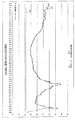
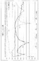
- FIG. 14 is a graph showing a comparison characteristic indicating an effect of the tuning plate of the first antenna device 301.
- 14A shows a limit line indicating -10.9 dB
- FIG. 14B shows standard characteristics of the first antenna device 301 (with a tuning plate 45)
- FIG. 14C shows a case where the tuning plate 45 is not provided.
- D shows the characteristics when the tuning plate 45 has not been adjusted.
- the characteristic (c) when there is no tuning plate and the characteristic (d) when the tuning plate 45 is not adjusted exceed the limit line (a) of -10.9 dB in the vicinity of 500 MHz to 1 GHz.
- the standard characteristic with the tuning plate 45
- a strong resonance of ⁇ 35 dB to ⁇ 39 dB is generated around 1.9 GHz. .
- FIG. 15 is a graph showing comparative characteristics showing the effect of the tuned plating plate of the first antenna device 301.
- 15A shows a limit line indicating -10.9 dB
- FIG. 15B shows standard characteristics of the first antenna device 301 (with a tuning plating plate 55)
- FIG. (D) shows the characteristics when the entire inner surface of the base 11 is plated.
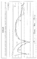
- FIG. 16 is a graph showing comparative characteristics indicating the effect of the conductive cushion of the first antenna device 301.
- 16A shows a limit line indicating -10.9 dB
- FIG. 16B shows standard characteristics of the first antenna device 301 (with the conductive cushion 80)
- FIG. The characteristics when there is no conductive cushion 80 are shown
- the graph (d) shows the characteristics when the conductive cushion 80 is loaded.
- the characteristic (c) without the conductive cushion 80 exceeds the limit line (a) of -10.9 dB in the range of 500 MHz to 6 GHz.
- the characteristic (d) when the conductive cushion 80 is loaded exceeds the limit line (a) of -10.9 dB in the vicinity of 700 MHz to 1.2 GHz, while it is -35 dB to -40 in the vicinity of 3.8 GHz to 4 GHz. A strong resonance of dB is generated.
- the standard characteristic the conductive cushion is provided
- the conductive cushion 80 provided in the first antenna device 301 is adjusted (b)
- (b) is effective in a high frequency range of 6 GHz.
- FIG. 17 is an impedance chart used for impedance matching of the antenna device 1.
- the impedance chart is used for designing RF (Radio Frequency) or microwave impedance matching.
- the horizontal axis represents the real part (resistance component) of the impedance Z, and the vertical axis represents the imaginary part (reactance component).
- the angle displayed in the surroundings is the phase ⁇ (ANG: angle) of the voltage reflection coefficient.
- the center Z0 corresponds to a state in which the load and the transmission line are matched, and is usually 50 ⁇ . However, in the impedance chart, the center is normalized to the input impedance and expressed as 1.0.
- the antenna device 1 includes an antenna element 30 having an arc peripheral edge 32 at least at a part of a peripheral edge thereof, and a feeder 33 at a part of the arc peripheral edge, and an insulation element on the back side of the antenna element.
- a tuning plate 45 which is formed of a thin plate-shaped conductor longer than the maximum diameter of the antenna element and which has a capacitive coupling portion 45a in a region facing the back surface of the antenna element;
- the radio wave absorber 50 is disposed on the back side of the capacitive coupling portion of the plate and absorbs radio waves radiated from the back side of the antenna element, and is folded back to the back side of the radio wave absorber through the side surface of the radio wave absorber.
- the tuning plating plate 55 for electrically connecting a tuning plating plate and electrically connected to the grounding member (ground plate 85), characterized in that it comprises a.
- a radio wave absorber is arranged as a member for improving the return loss characteristic of the frequency radiated from the antenna element 30 in all frequency bands, and a tuning plate and a tuning plating plate are used as members for improving the frequency characteristics in each frequency band.
- impedance matching can be achieved in the entire frequency band of 600 MHz to 6 GHz, and VSWR can be set to 1.8 or less.
- the antenna device 1 is characterized in that the tuning frequency with the antenna element 30 is adjusted by changing the area of the capacitive coupling portion 45a of the tuning plate 45. Further, the tuning frequency of the tuning plate is 1.3 GHz to 4.5 GHz. According to this aspect, by coupling the antenna element and the tuning plate capacitively, the return loss characteristic in a specific frequency band, specifically, an intermediate frequency of 1.3 GHz to 4.5 GHz can be improved and matched.
- the antenna device 1 is characterized in that the antenna element 30 and the tuning plating plate 55 are capacitively coupled via the tuning plate 45.
- the tuning frequency of the tuning plating plate is 600 MHz to 1.5 GHz. According to this aspect, by coupling the antenna element and the tuning plating plate capacitively, the return loss characteristics in a specific frequency band, specifically, a relatively low frequency of 600 MHz to 1.5 GHz can be improved and matched.
- the antenna device 1 includes a center conductor 64 whose one end in the axial direction 64a is electrically connected to the feeding unit 33, and an outer conductor surrounding the other end in the axial direction of the center conductor via the insulator 63.
- a signal input member 61 having an outer conductor and elastically deformable conductive cushions 80a and 80b sandwiching an outer conductor are provided.
- power is supplied to the antenna element 30 by the signal input member.
- the conductive cushion 80 is disposed so that the longitudinal direction extends in a direction intersecting with the axial direction of the signal input member 61, and by adjusting the longitudinal length of the conductive cushion.
- the tuning frequency with the antenna element 30 is adjusted.
- the tuning frequency of the conductive cushion is 4.5 GHz to 6 GHz. According to this aspect, the return loss characteristic at 4.5 GHz to 6 GHz can be improved by the conductive cushion.
- ground member (ground plate 85) is electrically connected to the outer conductor 62 of the signal input member 61.
- the tuning plate 45 and the tuning plated plate 55 are grounded via the ground member, and contribute to and improve the return loss characteristic in a required frequency band.
- the antenna device 2 is characterized in that the NFC board 90 is disposed on the front side of the antenna element 30.
- the NFC board is provided between an information processing device such as a personal computer that can be connected via a wired communication connection terminal such as a USB terminal provided on the NFC board, and a wireless communication terminal that can perform communication based on the NFC communication standard.
- This is a board that enables two-way communication between the two.
- the information processing device acquires a communication result from the wireless communication terminal by NFC, and the information processing device sends a communication result to the wireless communication terminal.
- an instruction can be transmitted by the NFC to generate a radio wave according to the test content.
Landscapes
- Physics & Mathematics (AREA)
- Electromagnetism (AREA)
- General Physics & Mathematics (AREA)
- Details Of Aerials (AREA)
- Waveguide Aerials (AREA)
- Control And Other Processes For Unpacking Of Materials (AREA)
- Burglar Alarm Systems (AREA)
- Radar Systems Or Details Thereof (AREA)
Abstract
Description
1つの無線局が数百MHz~数GHzに亘る超広帯域な周波数帯を利用する無線システムとして、UWB(Ultra Wide Band)無線システムが知られている。
特許文献1には、平面視左右線対称で略ホームベース型の平板状のアンテナ部と、アンテナ部と同一基板面に配置されてアンテナ部と容量結合される概略平板矩形状のグランド部とを備えたUWBアンテナ装置が記載されている。 2. Description of the Related Art In recent years, in mobile communication terminals such as mobile phones and smartphones, transmission / reception frequencies of radio waves extend over a plurality of bands. When conducting a communication test of these mobile communication terminals, it was necessary to prepare an antenna matched to each specific frequency band to be measured and switch the antenna for each frequency band .
A UWB (Ultra Wide Band) wireless system is known as a wireless system in which one wireless station uses an ultra-wideband frequency band ranging from several hundred MHz to several GHz.
本発明は上述の事情に鑑みてなされたものであり、1つのアンテナ装置で600MHz~6GHzの周波数帯域全体に連続的に整合させることにより、アンテナ装置を切り替えることなく、使用周波数帯域が異なる複数種類の通信装置との通信を可能とするアンテナ装置を提供することを目的とする。 However, in the antenna device described in
The present invention has been made in view of the above circumstances, and a single antenna device continuously matches the entire frequency band of 600 MHz to 6 GHz, so that a plurality of types of antennas having different frequency bands can be used without switching the antenna device. It is an object of the present invention to provide an antenna device capable of communicating with another communication device.
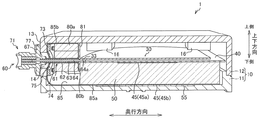
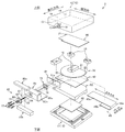
図1(a)、(b)は、本発明の第一の実施形態に係るアンテナ装置の外観を示した斜視図である。図2は、本発明の第一の実施形態に係るアンテナ装置の分解斜視図である。図3は、アンテナ装置を信号入力部材に沿って切断した断面を示す斜視図である。図4は、アンテナ装置を信号入力部材に沿った面とこれに直交する面とによって切断した断面を示す斜視図である。
本実施形態に係るアンテナ装置は、アンテナエレメントと同調板との間に絶縁体が挿入されている点に特徴がある。
以下の説明においては、電磁波が輻射される側を上側(上面)又は表側(表面)とし、その反対側を下側(下面)又は裏側(裏面)として説明する。また、同軸コネクタの延在方向を奥行き方向とし、上下方向及び奥行き方向と直交する方向を幅方向として説明する。 [First Embodiment: Normal Model]
FIGS. 1A and 1B are perspective views showing the appearance of an antenna device according to a first embodiment of the present invention. FIG. 2 is an exploded perspective view of the antenna device according to the first embodiment of the present invention. FIG. 3 is a perspective view showing a cross section of the antenna device cut along the signal input member. FIG. 4 is a perspective view showing a cross section of the antenna device cut by a surface along the signal input member and a surface orthogonal to the surface.
The antenna device according to the present embodiment is characterized in that an insulator is inserted between the antenna element and the tuning plate.
In the following description, the side from which the electromagnetic wave is radiated is referred to as the upper side (upper surface) or the front side (front surface), and the opposite side is referred to as the lower side (lower surface) or the back side (back surface). In addition, the extending direction of the coaxial connector is referred to as a depth direction, and a direction perpendicular to the vertical direction and the depth direction is referred to as a width direction.
アンテナ装置1は、各構成部材を収容する中空の収容部を形成するケース10を備え、ケース10は、概略矩形状のベース11と、ベース11にネジ止め固定される上カバー12とを備える。上カバー12の幅方向に伸びる一の側面板13には、同軸コネクタ60の信号入力部材61を挿通する同軸部材挿通穴14と、同軸コネクタ60を側面板13にネジ止め固定するための挿通穴15が貫通形成されている。
ケース10の内部には、半円板状(或いは弓形状)のアンテナエレメント30が収容される。アンテナエレメント30の下方(裏面側)には、アンテナエレメント30と他の部材とを絶縁する第一絶縁板40と、ショートスタブとして機能する同調板45と、所定の厚さtを有した電波吸収体50と、同調メッキ板55と、が順次積層される。なお、図中符号16は、アンテナエレメント30をケース10内で位置決めするエレメントガイドである。 <Overview of antenna element area>
The
Inside the
図5は、アンテナ装置に組み付けられたアンテナエレメントを裏面側から観察した斜視図である。
アンテナエレメント30は、円形の銅板から一つの弦31で銅板を二つに切り分けたときできる2つの弓形状部分のうち、小さい方の弓形状部分を除去した形状を有する。アンテナエレメント30は、周縁部の少なくとも一部に円弧周縁部32を備えると共に、この円弧周縁部32の一部に給電部33を備える。アンテナエレメント30は、周縁部の他部に円弧周縁部32の端点間を接続する弦31を備える。 <Antenna element>
FIG. 5 is a perspective view of the antenna element assembled to the antenna device as viewed from the back side.
The
アンテナエレメント30は、円弧周縁部32の適所、より詳しくは円弧周縁部32の中心部に給電部33を有する。
アンテナエレメント30の大きさは、電波吸収体の誘電率による波長短縮の影響を考慮して決定した。電波吸収体がポリウレタンと仮定して誘電率5の時の波長短縮係数0.45を600MHzのλ/4に反映させると、短縮波長が56mmとなるため、直径56mmの円を初期形状とした。この円から徐々に直径を大きくして実験した結果から、最終的な円の直径を70mmとした。さらに600MHz付近で整合を取るために弓形状部分を除去して直線縁(弦31)を配する形状とし、弦31の寸法も、概ね600MHzのλ/4に短縮係数を反映したサイズが実験からもっとも良好な特性であったことから、弦31の寸法として約59mmを採用した。 The
The
The size of the
図2に戻り、第一絶縁板40は、アクリル板や塩ビ板等、絶縁性を有する合成樹脂により構成される。第一絶縁板40は、アンテナエレメント30と電波吸収体50とを絶縁する役割を果たす。第一絶縁板40は、アンテナエレメント30と同調板45とが電気的に接続せず、確実に絶縁状態を保持できる大きさに設定される。 <First insulating plate>
Returning to FIG. 2, the first insulating
同調板45は、アンテナエレメント30との対向面積に応じてアンテナエレメント30と容量結合してインピーダンス整合をとるスタブ(ショートスタブ)として機能する。
同調板45は、アンテナエレメント30の裏面側に絶縁された状態で対向配置される。同調板45は、アンテナエレメント30の最大径(最大幅)よりも長尺な薄板状の導電体により構成される。具体的には、同調板45は、概略帯板形状であり、長手方向長115mm、幅方向長25mm、厚さ0.05mmの黄銅箔(真鍮箔、導電体)により構成される。 <Tuned board>
The tuning
The tuning
同調板45は、J字状、U字状に湾曲変形されるか、又は角U字状に折り曲げられることにより、容量結合部45aとアース部45bとが電波吸収体50の表面側と裏面側に夫々添設されて、電波吸収体50を厚さ方向に挟む構成である。この構成により、容量結合部45aがアンテナエレメント30の裏面と第一絶縁板40を介して対向し、長手方向の他端部に設けたアース部45bが同調メッキ板55の表面と直接に対向する。 In the
The tuning
本例において、容量結合部45aは、アンテナエレメント30の幅方向の全域に亘ってアンテナエレメント30と対向している。言い換えれば、容量結合部45aの長手方向長は、アンテナエレメント30の直径と略同等の長さかこれ以上の長さを有するように設定される。従って、アンテナエレメント30との容量結合量は、容量結合部45aの短手方向長(アンテナ装置1の奥行き方向における長さ)によって調整される。
ここで、アンテナエレメント30と容量結合部45aの間に形成される結合容量C1、容量結合部45aの長手方向長により形成されるインダクタンスL1をそれぞれ調整する際、インピーダンスチャート(図17参照)を用いた周知の整合戦略手法に従って、50Ωの同軸ケーブルにインピーダンス整合をとる。
例えば、本例に係る同調板45の同調周波数を1.3GHz~4.5GHzに設定した場合、同調板45の長手方向長は115mm、容量結合部45aの長手方向長は74mm、幅方向長は25mmのように設定することができる。 The
In this example, the
Here, when adjusting the coupling capacitance C1 formed between the
For example, when the tuning frequency of the
電波吸収体50は、同調板45の容量結合部45aの裏面側に配置される。電波吸収体50は、アンテナエレメント30の裏面側から輻射される電波を吸収し、減衰させる。
電波吸収体50は、炭素粉末を分散し発泡させた発泡ポリウレタンにより構成される。電波吸収体50は、アンテナエレメント30の全面を覆う大きさ(面積)を有する。電波吸収体50の電波吸収特性はその厚さtによって決定される。
電波吸収体50は、アンテナ装置1が対応する(整合可能な)周波数の全域において電波を吸収する性能を有していればよい。本例において、電波吸収体50にはE&Cエンジニアリング株式会社製のECOSORB AN74(厚さ19mm、対応周波数500MHz~9GHz)を採用することができる。 <Electromagnetic wave absorber>
The
The
The
同調メッキ板55は、電波吸収体50の裏面側に配置される。同調メッキ板55の上面の一部は電波吸収体50の裏面と直接に対向して接触し、他部は同調板45のアース部45b及び後述するアース板(アース部材)85の長手方向の一端部85aを介して電波吸収体50の裏面と対向する。同調メッキ板55は、同調板45のアース部45bと面接触することにより電気的に接続し、アース板85の長手方向の一端部85aと面接触することにより電気的に接続する。 <Synchronized plating plate>
The
同調メッキ板55は同調板45を介して、アンテナエレメント30と容量結合して、主に比較的低い周波数帯である600MHz~1.5GHz帯域の電磁波の同調を取る役割を果たす。なお、同調メッキ板55は、実験の結果から、その面積の85%以上がアンテナエレメント30の直下に位置するように配置されていれば、上記役割を果たすには十分である。
また、同調メッキ板55は、アンテナ装置1の下面から外部への電波漏洩を防止するシールドの役割を果たす。 In the
The
Further, the
アンテナエレメント30に給電すると共に、アンテナ装置1の各部をアースする信号入力部材周辺の構成について説明する。
アンテナ装置1は、中心導体64がアンテナエレメント30の給電部33に電気的・機械的に固定された信号入力部材61を有する同軸コネクタ60と、少なくとも外周部(外面)に布状の導電体を有し、信号入力部材61の外導体62を挟持する弾性的に変形可能な導電性クッション80(80a,80b)と、信号入力部材61の外導体62と導通すると共に、一部が同調板45のアース部45bと接触するアース板(アース部材)85と、を備える。
導電性クッション80とアンテナエレメント30との間には両者を絶縁する第二絶縁板81が挿入される。第二絶縁板81には、信号入力部材61の中心導体64を側面板13側からアンテナエレメント30側に向けて通過させるスリット81aが上下方向に形成されている。 <Summary of power supply and ground area>
The configuration around the signal input member that feeds the
The
Between the
同軸コネクタ60は、軸方向一端部に配置された信号入力部材61と、軸方向中間部に配置されて信号入力部材61の外導体62と導通したフランジ部67と、軸方向他端部に配置されて信号入力部材61の各導体と導通し、伝送ケーブルを着脱自在に接続するコネクタ部71(同軸レセプタクル)と、を備える。 <Coaxial connector>
The
中心導体64の軸方向一端部64aは、外導体62の軸方向一端縁を超えて外方に突出している。言い換えれば、外導体62は、中心導体64を軸方向の他端部において包囲する。外部に露出した中心導体64の軸方向一端部64aは、アンテナエレメント30の裏面に設けた給電部33に対して、はんだにより固定されている。信号入力部材61の軸方向は、アンテナ装置1を基準としてその奥行き方向に伸びており、アンテナエレメント30に対しては円弧周縁部32の接線に沿った方向、即ち、弦31と直交する方向に伸びている。 The
One end portion 64a of the
同軸コネクタ60は、コネクタプレート73のネジ穴74と、側面板13及びフランジ部67に夫々形成された挿通穴15,68とを連通させた状態にて、ネジ77の軸部を各穴内に挿入してネジ穴74に螺着することにより、上カバー12の側面板13に固定される。コネクタプレート73は、導電性のネジ77を介してフランジ部67と導通するため、コネクタプレート73は信号入力部材61の外導体62とも導通する。 An
The
アース板85は、本実施形態に係るアンテナ装置1が対応する全ての周波数帯域(600MHz~6GHz)において、VSWR(Voltage Standing Wave Ratio)特性を改善する手段である。
アース板85は、概略矩形形状であり、厚さ0.05mmの黄銅箔(真鍮箔)から構成される。アース板85の幅方向長は45mmで導電性クッション80の幅方向長と同一である。アース板85の幅方向と直交する方向における長さ(長手方向長)は、アース板85が導電性クッション80と同調メッキ板55と同調板45を、直接的に又は間接的にアース可能な長さに設定される。 <Earth plate>
The
The
なお、長手方向の他端部85b側は、第二絶縁板81を超えてアンテナエレメント30側には突出しない長さに設定される。即ち、アース板85は、アンテナエレメント30の上面とは対向しない。 Part of the ground plate 85 (in this example, the middle portion in the longitudinal direction) is disposed between the inner surface of the
The
導電性クッション80(80a,80b)は、信号入力部材61の外導体62を上下方向から間に挟んで保持することにより外導体62と導通する。また、導電性クッション80は、外導体62に押圧されて変形することで、アンテナ装置1の内部で信号入力部材61の上下方向位置を安定させる役割を果たす。
導電性クッション80は、弾性的に変形可能な発泡体を芯材として、その外周部に導電性の布材を一体化させることにより構成されている。発泡体は、発泡ポリウレタン、発泡クロロプレンゴム、ゴムスポンジ等の絶縁体から構成されることが望ましい。発泡体には導電性のウレタンウォーム等を用いることも可能である。導電性の布材は例えば金属繊維を織るか又は編むこと等により形成されたメッシュ状の導電体であり、例えば銅にニッケルメッキを施した金属線材等からメッシュ形成することができる。なお、導電性の布材は不織布でもよい。 <Conductive cushion>
The conductive cushion 80 (80a, 80b) is electrically connected to the
The
ここで、導電性クッション80とアース板85の間に形成される結合容量C2、導電性クッション80の長さにより形成されるインダクタンスL2をそれぞれ調整する際、インピーダンスチャート(図17参照)を用いた周知の整合戦略手法に従って、50Ωの同軸ケーブルにインピーダンス整合をとる。
例えば、信号入力部材61の上側に配置される導電性クッション80aは、厚さ(上下方向長)4mm×幅(奥行方向長)10mm×長さ45mmとすることができ、信号入力部材61の下側に配置される導電性クッション80bは、厚さ8mm×幅10mm×長さ45mmとすることができる。本例において導電性クッション80の同調周波数は、4.5GHz~6GHzである。 The
Here, when adjusting the coupling capacitance C2 formed between the
For example, the
アンテナ装置1が受信状態にある場合、外部から到来した電波は、アンテナエレメント30で拾われ、信号入力部材61を通じてコネクタ部71へと誘導される。
一方、アンテナ装置1が送信状態にある場合、コネクタ部71へ供給された電波は、信号入力部材61を通じてアンテナエレメント30に供給され、空間に電波が放射される。 <Flow of electricity>
When the
On the other hand, when the
以上のように、本実施形態によれば、アンテナ装置1が対応する(整合可能な)周波数(600MHz~6GHz)の波長/4(125mm~12.5mm)に波長短縮を考慮した波長に対して十分に大きなアンテナエレメント30を採用し、各周波数帯に応じてリターンロス特性を改善する部材を取り付けた。具体的には、同調メッキ板55は、主として600MHz~1.5GHz帯域のリターンロス特性を改善し、同調板45は主として1.3GHz~4.5GHz帯のリターンロス特性を改善し、導電性クッション80は主として4.5~6GHz帯域のリターンロス特性を改善する。また、電波吸収体50は、500MHz~9GHz帯域においてリターンロス特性を改善する。
このように、各周波数帯に応じてリターンロス特性を改善する部材を取り付けたことにより、広範囲の周波数帯域における電波計測を一つのアンテナ装置にて実施することが可能となる。また、誘電率を活用した整合を図ることにより波長が短縮化され、アンテナ装置を小型化することが可能となる。 <Effect>
As described above, according to the present embodiment, the
As described above, by installing the member for improving the return loss characteristic according to each frequency band, it is possible to perform radio wave measurement in a wide frequency band with one antenna device. Further, the matching is performed by utilizing the dielectric constant, whereby the wavelength is shortened, and the antenna device can be downsized.
図6(a)、(b)は、本発明の第二の実施形態に係るアンテナ装置の外観を示した斜視図である。図7は、本発明の第二の実施形態に係るアンテナ装置の分解斜視図である。
本実施形態に係るアンテナ装置は、NFC(Near Field Communication)に基づく無線通信を行うNFC基板を備えた点に特徴がある。以下、第一の実施形態と同一の構成については同一の符号を付してその説明を省略する。 [Second embodiment: NFC model]
FIGS. 6A and 6B are perspective views showing the appearance of an antenna device according to a second embodiment of the present invention. FIG. 7 is an exploded perspective view of the antenna device according to the second embodiment of the present invention.
The antenna device according to the present embodiment is characterized in that it has an NFC board that performs wireless communication based on NFC (Near Field Communication). Hereinafter, the same components as those of the first embodiment are denoted by the same reference numerals, and description thereof is omitted.
<アンテナシステム、及び計測システム>
図8(a)は本発明の一実施形態に係るアンテナ装置を用いたアンテナシステム、及び計測システムを示すブロック図、図8(b)は当該計測システムの校正に用いるキャリブレーションキットを示す斜視図である。
図8(a)に示すアンテナシステム300は、1対のアンテナ装置を備え、各アンテナ装置を第一アンテナ装置301及び第二アンテナ装置303とし、第一アンテナ装置301から放射された電波を、第一アンテナ装置301の放射方向に対向して配置された第二アンテナ装置303により受信する。 [Explanation of graph]
<Antenna system and measurement system>
FIG. 8A is a block diagram showing an antenna system and a measurement system using the antenna device according to one embodiment of the present invention, and FIG. 8B is a perspective view showing a calibration kit used for calibrating the measurement system. It is.
The
さらに、ネットワークアナライザ315のモニタ端子305mとモニタ313の端子313mとの間にモニタケーブル311を接続している。なお、ネットワークアナライザ315には、例えばアンリツ株式会社製のMS46322Bを用いている。
アンテナ装置は、被測定物に対して近接(密着)して配置しておき、例えば被測定物から放射される電波を測定するために用いる。被測定物としては、携帯電話器、モバイル端末等の電磁波を発生するものを対象としており、例えば、600MHz~6GHzの周波数帯を利用する通信機器(サブ6)を対象としている。
計測システム310は、アンテナシステム300に備えられた第一アンテナ装置301と第二アンテナ装置303との間の結合特性、反射減衰量特性を測定することに適している。 The
Further, a
The antenna device is arranged in close proximity (close contact) to an object to be measured, and is used, for example, to measure a radio wave radiated from the object to be measured. The device under test is a device that generates electromagnetic waves, such as a mobile phone and a mobile terminal. For example, the device under test is a communication device (sub 6) that uses a frequency band of 600 MHz to 6 GHz.
The
さらに、第一アンテナ装置301と第二アンテナ装置303との間に、被測定物を配置することで、被測定物から放射される電波、又は、被測定物で受信された場合に、被測定物による影響度合いを測定することができる。 As described above, the
Further, by disposing the device under test between the
キャリブレーションキット320には、コネクタ320S(SHORT)、コネクタ320o(OPEN)、コネクタ320L(LOAD)、コネクタ320T(THRU)という4つのコネクタを備えている。なお、キャリブレーションキット320には、例えばアンリツ株式会社製のTOSLKF50A-40を用いている。 In the
The
図9は、図8に示す計測システムのキャリブレーション手順を示すフローチャートである。詳しくは、アンテナ装置1の反射減衰量特性、結合特性の測定に先だって行う、計測システム310のキャリブレーション手順を示している。
ステップS5では、ネットワークアナライザ315に対して測定周波数(例えば500MHz~6.2GHz)を入力する。
ステップS10では、ネットワークアナライザ315に対してキャリブレーションCALモードに設定する。
ステップS15では、ネットワークアナライザ315の端子P1に接続されている同軸ケーブル307の先端にキャリブレーションキットのコネクタ320Sを接続して、同軸ケーブル307の先端を短絡状態(SHORT)にする。
ステップS20では、ユーザの操作に応じてネットワークアナライザ315が測定器内演算を行う。
ステップS25では、ネットワークアナライザ315の端子P1に接続されている同軸ケーブル307の先端にキャリブレーションキットのコネクタ320oを接続して、同軸ケーブル307の先端を開放状態(OPEN)にする。
ステップS30では、ユーザの操作に応じてネットワークアナライザ315が測定器内演算を行う。
ステップS35では、ネットワークアナライザ315の端子P1に接続されている同軸ケーブル307の先端にキャリブレーションキットのコネクタ320Lを接続して、同軸ケーブル307の先端に負荷(例えば50Ω)が接続された負荷状態(LOAD)にする。
ステップS40では、ユーザの操作に応じてネットワークアナライザ315が測定器内演算を行う。 <Measurement system calibration procedure>
FIG. 9 is a flowchart showing a calibration procedure of the measurement system shown in FIG. More specifically, the figure shows a calibration procedure of the
In step S5, a measurement frequency (for example, 500 MHz to 6.2 GHz) is input to the
In step S10, the
In step S15, the
In step S20, the
In step S25, the connector 320o of the calibration kit is connected to the end of the
In step S30, the
In step S35, the
In step S40, the
ステップS50では、ユーザの操作に応じてネットワークアナライザ315が測定器内演算を行う。
ステップS55では、ネットワークアナライザ305の端子P2に接続されている同軸ケーブル309の先端にキャリブレーションキットのコネクタ320oを接続して、同軸ケーブル309の先端を開放状態(OPEN)にする。
ステップS60では、ユーザの操作に応じてネットワークアナライザ315が測定器内演算を行う。
ステップS65では、ネットワークアナライザ315の端子P2に接続されている同軸ケーブル309の先端にキャリブレーションキットのコネクタ320Lを接続して、同軸ケーブル309の先端に負荷(例えば50Ω)が接続された負荷状態(LOAD)にする。
ステップS70では、ユーザの操作に応じてネットワークアナライザ315が測定器内演算を行う。 In step S45, the
In step S50, the
In step S55, the connector 320o of the calibration kit is connected to the end of the
In step S60, the
In step S65, the
In step S70, the
ステップS70では、ユーザの操作に応じてネットワークアナライザ315が測定器内演算を行う。
この結果、ネットワークアナライザ315、同軸ケーブル307、309を含む計測システムに対して、設定された周波数帯において振幅特性、反射減衰量特性、位相特性等をフラットな状態に校正することができる。 In step S75, the
In step S70, the
As a result, for the measurement system including the
図10は、図8に示す計測システムにおいて行う反射減衰量測定手順を示すフローチャートである。
ステップS105では、ネットワークアナライザ315の端子P1に接続されている同軸ケーブル307の先端に第一アンテナ装置301のコネクタを接続して、測定可能状態にする。
ステップS110では、ユーザの操作に応じてネットワークアナライザ315が測定器内演算を行い、モニタ313に反射減衰量を表示する。この際、ネットワークアナライザ315の端子P1から出力された周波数帯のスイープ中の電力が、第一アンテナ装置301で反射され、第一アンテナ装置301から帰ってきた電力を測定する。 <Return loss measurement procedure>
FIG. 10 is a flowchart showing a return loss measuring procedure performed in the measurement system shown in FIG.
In step S105, the connector of the
In step S110, the
図11は、図8に示す計測システムにおいて行われる結合損失特性の測定手順を示すフローチャートである。
ステップS155では、ネットワークアナライザ315の端子P1に接続されている同軸ケーブル307の先端に第一アンテナ装置301のコネクタを接続して、測定可能状態にする。
ステップS160では、ネットワークアナライザ315が測定器内演算を行い、モニタ313に第一アンテナ装置301の反射減衰量を表示する。
ステップS165では、ネットワークアナライザ315の端子P2に接続されている同軸ケーブル309の先端に第二アンテナ装置303のコネクタを接続して、測定可能状態にする。
ステップS170では、ネットワークアナライザ315が測定器内演算を行い、モニタ313に第二アンテナ装置303の反射減衰量を表示する。
ステップS175では、第一アンテナ装置301と第二アンテナ装置303とを対向して近接(密接)する。
ステップS180では、ネットワークアナライザ315が測定器内演算を行い、第一アンテナ装置301と第二アンテナ装置303の間の結合特性、及び反射減衰量をモニタ313に表示する。 <Measurement procedure of coupling loss characteristics>
FIG. 11 is a flowchart showing a procedure for measuring the coupling loss characteristic performed in the measurement system shown in FIG.
In step S155, the connector of the
In step S <b> 160, the
In step S165, the connector of the
In step S170, the
In step S175, the
In step S180, the
図12は、第一の実施形態において構成された第一アンテナ装置301がノーマルモデルである場合の反射減衰量の標準特性を示すグラフ図である。
図12において、(a)は-10.9dBを示すリミットラインであり、(b)は第一アンテナ装置301の標準特性を示す。
第一アンテナ装置301がノーマルモデルである場合、周波数600MHz~6GHzの帯域において、反射減衰量(リターンロス)が-10.9dB以上(VSWRであると1.8以下)の特性を示している。 <Standard characteristics of normal model>
FIG. 12 is a graph illustrating standard characteristics of return loss when the
In FIG. 12, (a) is a limit line indicating -10.9 dB, and (b) shows standard characteristics of the
In the case where the
図13は、第二の実施形態において構成された第一アンテナ装置301がNFCモデルである場合の反射減衰量の標準特性を示すグラフ図である。
図13において、(a)は-10.9dBを示すリミットラインであり、(b)は第一アンテナ装置301の標準特性を示す。
第一アンテナ装置301がNFCモデルである場合、NFC基板90が所定の面積を有する両面基板により構成されているため、周波数600MHz~6GHzの帯域の反射減衰量(リターンロス)に影響を与える。
しかし、(b)に示すように、周波数600MHz~6GHzの帯域において、反射減衰量(リターンロス)が-10.9dB以上(VSWRであると1.8以下)の特性を示している。 <Standard characteristics of NFC model>
FIG. 13 is a graph showing standard characteristics of return loss when the
13A shows a limit line indicating -10.9 dB, and FIG. 13B shows standard characteristics of the
When the
However, as shown in (b), in the frequency band of 600 MHz to 6 GHz, the return loss (return loss) shows a characteristic of -10.9 dB or more (1.8 or less for VSWR).
図14は、第一アンテナ装置301の同調板による効果を表す比較特性を示すグラフ図である。
図14において、(a)は-10.9dBを示すリミットラインであり、(b)は第一アンテナ装置301の標準特性(同調板45あり)を示し、(c)は同調板45が無い場合の特性を示し、(d)は同調板45が未調整である場合の特性を示している。
同調板が無い場合の特性(c)、同調板45が未調整である場合の特性(d)では、500MHz~1GHz付近で-10.9dBのリミットライン(a)を超えている。
これに対して、第一アンテナ装置301に設けられた同調板45が調整された標準特性(同調板45あり)(b)では1.9GHz付近に-35dB~-39dBの強い共振を生じている。 <Effect of tuning plate>
FIG. 14 is a graph showing a comparison characteristic indicating an effect of the tuning plate of the
14A shows a limit line indicating -10.9 dB, FIG. 14B shows standard characteristics of the first antenna device 301 (with a tuning plate 45), and FIG. 14C shows a case where the
The characteristic (c) when there is no tuning plate and the characteristic (d) when the
On the other hand, in the standard characteristic (with the tuning plate 45) in which the
図15は、第一アンテナ装置301の同調メッキ板による効果を表す比較特性を示すグラフ図である。
図15において、(a)は-10.9dBを示すリミットラインであり、(b)は第一アンテナ装置301の標準特性(同調メッキ板55あり)を示し、(c)は同調メッキ板55が無い場合の特性を示し、(d)はベース11の内面を全メッキした場合の特性を示している。
同調メッキ板55が無い場合の特性(c)、同調メッキ板55が未調整である場合の特性(d)では、500MHz~1.2GHz付近で-10.9dBのリミットライン(a)に接近している。
これに対して、第一アンテナ装置301に設けられた同調メッキ板55が調整された標準特性(同調メッキ板55あり)(b)では1.9GHz付近に-35dB~-39dBの強い共振を生じている。 <Effect of tuning plating plate>
FIG. 15 is a graph showing comparative characteristics showing the effect of the tuned plating plate of the
15A shows a limit line indicating -10.9 dB, FIG. 15B shows standard characteristics of the first antenna device 301 (with a tuning plating plate 55), and FIG. (D) shows the characteristics when the entire inner surface of the
The characteristic (c) when there is no
On the other hand, in the standard characteristic (with the tuning plating plate 55) in which the
図16は、第一アンテナ装置301の導電性クッションによる効果を表す比較特性を示すグラフ図である。
図16は、(a)は-10.9dBを示すリミットラインであり、(b)は第一アンテナ装置301の標準特性(導電性クッション80あり)を示し、(c)は標準特性に対して導電性クッション80が無い場合の特性を示し、(d)は導電性クッション80を装填した場合の特性を示している。
導電性クッション80が無い場合の特性(c)では、500MHz~6GHzにおいて-10.9dBのリミットライン(a)を超えている。
導電性クッション80を装填した場合の特性(d)では、700MHz~1.2GHz付近で-10.9dBのリミットライン(a)を超え、一方、3.8GHz~4GHz付近に-35dB~-40数dBの強い共振を生じている。
これに対して、第一アンテナ装置301に設けられた導電性クッション80が調整された標準特性(導電性クッションあり)(b)では、1.9GHz~2GHz付近に-35dB~-39dBの強い共振を生じている。特に、(b)では、6GHzの高周波域に効果がある。 <Effect of conductive cushion>
FIG. 16 is a graph showing comparative characteristics indicating the effect of the conductive cushion of the
16A shows a limit line indicating -10.9 dB, FIG. 16B shows standard characteristics of the first antenna device 301 (with the conductive cushion 80), and FIG. The characteristics when there is no
The characteristic (c) without the
The characteristic (d) when the
On the other hand, in the standard characteristic (the conductive cushion is provided) in which the
図17は、アンテナ装置1のインピーダンス整合をとるために用いるインピーダンスチャートである。
インピーダンスチャートは、RF(Radio Frequency)やマイクロ波のインピーダンス整合の設計に用いられ、横軸はインピーダンスZの実部(抵抗成分)であり、縦軸が虚部(リアクタンス成分)を表す。左端はZ=0(全透過)、右端はZ=∞(全反射)に相当する。また、周囲に表示している角度は、電圧反射係数の位相θ(ANG:angle)である。中心Z0は、負荷と伝送路が整合した状態に相当し、通常は50Ωであるが、インピーダンスチャートでは、入力インピーダンスを基準に正規化して1.0で表現している。 <Impedance chart>
FIG. 17 is an impedance chart used for impedance matching of the
The impedance chart is used for designing RF (Radio Frequency) or microwave impedance matching. The horizontal axis represents the real part (resistance component) of the impedance Z, and the vertical axis represents the imaginary part (reactance component). The left end corresponds to Z = 0 (total transmission), and the right end to Z = ∞ (total reflection). The angle displayed in the surroundings is the phase θ (ANG: angle) of the voltage reflection coefficient. The center Z0 corresponds to a state in which the load and the transmission line are matched, and is usually 50Ω. However, in the impedance chart, the center is normalized to the input impedance and expressed as 1.0.
<第一の実施態様>
本態様に係るアンテナ装置1は、周縁部の少なくとも一部に円弧周縁部32を備えると共に、該円弧周縁部の一部に給電部33を備えたアンテナエレメント30と、アンテナエレメントの裏面側に絶縁された状態で対向配置され、アンテナエレメントの最大径よりも長尺な薄板状の導電体により構成されると共に、アンテナエレメントの裏面と対向する領域を容量結合部45aとする同調板45と、同調板の容量結合部の裏面側に配置されて、アンテナエレメントの裏面側から輻射される電波を吸収する電波吸収体50と、電波吸収体の側面部を経て該電波吸収体の裏面側に折り返される同調板の余長部分(45b、45c)と、電波吸収体の裏面側に配置されて、表面に金属メッキ膜が形成されると共に、同調板の余長部分に設けたアース部45bと電気的に接続する同調メッキ板55と、同調メッキ板と電気的に接続するアース部材(アース板85)と、を備えることを特徴とする。
本態様によれば、1つのアンテナ装置で600MHz~6GHzの周波数帯域全体に連続的に整合させることにより、アンテナ装置を切り替えることなく、使用周波数帯域が異なる複数種類の通信装置との通信を可能とするアンテナ装置を提供することができる。
即ち、アンテナエレメント30から輻射される周波数の反射減衰量特性を全周波数帯域において改善する部材として電波吸収体を配置し、周波数特性を各周波数帯域において改善する部材として、同調板と同調メッキ板を配置することによって、600MHz~6GHzの周波数帯域全体においてインピーダンス整合が取れ、VSWRが1.8以下とすることができる。 [Summary of Embodiment Examples, Functions, and Effects of the Present Invention]
<First embodiment>
The
According to this aspect, by performing continuous matching over the entire frequency band of 600 MHz to 6 GHz with one antenna device, communication with a plurality of types of communication devices using different frequency bands can be performed without switching the antenna device. It is possible to provide an antenna device that performs
That is, a radio wave absorber is arranged as a member for improving the return loss characteristic of the frequency radiated from the
本態様に係るアンテナ装置1は、同調板45の容量結合部45aの面積を可変させることにより、アンテナエレメント30との同調周波数を調整することを特徴とする。
また、同調板の同調周波数は、1.3GHz~4.5GHzであることを特徴とする。
本態様によれば、アンテナエレメントと同調板とを容量結合させることにより、特定の周波数帯域、具体的には中間の周波数1.3GHz~4.5GHzにおける反射減衰量特性を改善し整合できる。 <Second and third embodiments>
The
Further, the tuning frequency of the tuning plate is 1.3 GHz to 4.5 GHz.
According to this aspect, by coupling the antenna element and the tuning plate capacitively, the return loss characteristic in a specific frequency band, specifically, an intermediate frequency of 1.3 GHz to 4.5 GHz can be improved and matched.
本態様に係るアンテナ装置1において、アンテナエレメント30と同調メッキ板55とは、同調板45を介して容量結合していることを特徴とする。
また、同調メッキ板の同調周波数は、600MHz~1.5GHzであることを特徴とする。
本態様によれば、アンテナエレメントと同調メッキ板とを容量結合させることにより、特定の周波数帯域、具体的には比較的低い周波数600MHz~1.5GHzにおける反射減衰量特性を改善し整合できる。 <Fourth and fifth embodiments>
The
The tuning frequency of the tuning plating plate is 600 MHz to 1.5 GHz.
According to this aspect, by coupling the antenna element and the tuning plating plate capacitively, the return loss characteristics in a specific frequency band, specifically, a relatively low frequency of 600 MHz to 1.5 GHz can be improved and matched.
本態様に係るアンテナ装置1は、軸方向一端部64aが給電部33に電気的に接続された中心導体64、及び、絶縁体63を介して中心導体の軸方向他端部を包囲する外導体62を備えた信号入力部材61と、少なくとも外周部に導電体を有し、外導体を挟持する弾性的に変形可能な導電性クッション80a,80bと、を備えることを特徴とする。
本態様においてはアンテナエレメント30に対して信号入力部材により給電するが、信号入力部材を導電性クッションによって挟むことにより、比較的高い周波数帯域の周波数特性を改善できる。 <Sixth embodiment>
The
In this embodiment, power is supplied to the
本態様に係るアンテナ装置1において、導電性クッション80は、長手方向が信号入力部材61の軸方向と交差する方向に伸びるように配置されており、導電性クッションの長手方向長を調整することによりアンテナエレメント30との同調周波数を調整することを特徴とする。
また、導電性クッションの同調周波数は、4.5GHz~6GHzであることを特徴とする。
本態様によれば、導電性クッションにより4.5GHz~6GHzの反射減衰量特性を改善できる。 <Seventh and eighth embodiments>
In the
In addition, the tuning frequency of the conductive cushion is 4.5 GHz to 6 GHz.
According to this aspect, the return loss characteristic at 4.5 GHz to 6 GHz can be improved by the conductive cushion.
本態様に係るアンテナ装置1において、
アース部材(アース板85)は信号入力部材61の外導体62と導通することを特徴とする。
本態様によれば、アース部材を介して、同調板45と同調メッキ板55とがアースされ、必要な周波数帯域での反射減衰量特性の改善に寄与し整合する。 <Ninth embodiment>
In the
The ground member (ground plate 85) is electrically connected to the
According to this aspect, the tuning
本態様に係るアンテナ装置2は、アンテナエレメント30の表面側にNFC基板90が配置されていることを特徴とする。
ここで、NFC基板は、NFC基板に設けたUSB端子等の有線通信用の接続端子を介して接続可能なパソコン等の情報処理装置と、NFC通信規格に基づく通信が可能な無線通信端末との間における双方向通信を可能にする基板である。
本態様によれば、アンテナ装置を用いて無線通信端末に係る通信試験を行う際に、情報処理装置が無線通信端末からNFCにより通信結果を取得すること、及び情報処理装置から無線通信端末に対してNFCにより試験内容に応じた電波を発生するように命令を送信することが可能となる。 <Tenth embodiment>
The
Here, the NFC board is provided between an information processing device such as a personal computer that can be connected via a wired communication connection terminal such as a USB terminal provided on the NFC board, and a wireless communication terminal that can perform communication based on the NFC communication standard. This is a board that enables two-way communication between the two.
According to this aspect, when performing a communication test related to the wireless communication terminal using the antenna device, the information processing device acquires a communication result from the wireless communication terminal by NFC, and the information processing device sends a communication result to the wireless communication terminal. Thus, an instruction can be transmitted by the NFC to generate a radio wave according to the test content.
Claims (10)
- 周縁部の少なくとも一部に円弧周縁部を備えると共に、該円弧周縁部の一部に給電部を備えたアンテナエレメントと、
前記アンテナエレメントの裏面側に絶縁された状態で対向配置され、前記アンテナエレメントの最大径よりも長尺な薄板状の導電体により構成されると共に、前記アンテナエレメントの裏面と対向する領域を容量結合部とする同調板と、
前記同調板の前記容量結合部の裏面側に配置されて、前記アンテナエレメントの裏面側から輻射される電波を吸収する電波吸収体と、
前記電波吸収体の側面部を経て該電波吸収体の裏面側に折り返される前記同調板の余長部分と、
前記電波吸収体の裏面側に配置されて、表面に金属メッキ膜が形成されると共に、前記同調板の余長部分に設けたアース部と電気的に接続する同調メッキ板と、
前記同調メッキ板と電気的に接続するアース部材と、を備えることを特徴とするアンテナ装置。 An antenna element having an arc peripheral part at least in a part of the peripheral part, and having a feeding part in a part of the arc peripheral part,
The antenna element is disposed opposite to the back side of the antenna element in an insulated state, is formed of a thin plate-shaped conductor longer than the maximum diameter of the antenna element, and capacitively couples a region facing the back surface of the antenna element. Tuning plate to be
A radio wave absorber arranged on the back side of the capacitive coupling portion of the tuning plate and absorbing radio waves radiated from the back side of the antenna element,
A surplus portion of the tuning plate that is folded back to the back surface side of the radio wave absorber through a side surface portion of the radio wave absorber,
A tuning plate that is arranged on the back side of the radio wave absorber, has a metal plating film formed on the surface, and is electrically connected to a ground portion provided on an extra length of the tuning plate;
An antenna device comprising: a ground member electrically connected to the tuning plating plate. - 前記同調板の前記容量結合部の面積を可変させることにより、前記アンテナエレメントとの同調周波数を調整することを特徴とする請求項1に記載のアンテナ装置。 2. The antenna device according to claim 1, wherein a tuning frequency with the antenna element is adjusted by changing an area of the capacitive coupling portion of the tuning plate. 3.
- 前記同調板の同調周波数は、1.3GHz~4.5GHzであることを特徴とする請求項1又は2に記載のアンテナ装置。 3. The antenna device according to claim 1, wherein a tuning frequency of the tuning plate is 1.3 GHz to 4.5 GHz.
- 前記アンテナエレメントと前記同調メッキ板とは、前記同調板を介して容量結合していることを特徴とする請求項1乃至3の何れか一項に記載のアンテナ装置。 4. The antenna device according to claim 1, wherein the antenna element and the tuning plating plate are capacitively coupled via the tuning plate. 5.
- 前記同調メッキ板の同調周波数は、600MHz~1.5GHzであることを特徴とする請求項1乃至4の何れか一項に記載のアンテナ装置。 (5) The antenna device according to any one of (1) to (4), wherein a tuning frequency of the tuning plating plate is 600 MHz to 1.5 GHz.
- 軸方向一端部が前記給電部に電気的に接続された中心導体、及び、絶縁体を介して前記中心導体の軸方向他端部を包囲する外導体を備えた信号入力部材と、
少なくとも外周部に導電体を有し、前記外導体を挟持する弾性的に変形可能な導電性クッションと、を備えることを特徴とする請求項1乃至5の何れか一項に記載のアンテナ装置。 A central conductor having one axial end electrically connected to the power supply unit, and a signal input member including an outer conductor surrounding the other axial end of the central conductor via an insulator;
The antenna device according to any one of claims 1 to 5, further comprising: a conductive cushion that has a conductor at least in an outer peripheral portion and elastically deforms and sandwiches the outer conductor. - 前記導電性クッションは、長手方向が前記信号入力部材の軸方向と交差する方向に伸びるように配置されており、前記導電性クッションの長手方向長を調整することにより前記アンテナエレメントとの同調周波数を調整することを特徴とする請求項6に記載のアンテナ装置。 The conductive cushion is arranged so that its longitudinal direction extends in a direction intersecting with the axial direction of the signal input member, and adjusts the tuning frequency with the antenna element by adjusting the longitudinal length of the conductive cushion. The antenna device according to claim 6, wherein the antenna device is adjusted.
- 前記導電性クッションの同調周波数は、4.5GHz~6GHzであることを特徴とする請求項6又は7に記載のアンテナ装置。 (8) The antenna device according to (6) or (7), wherein a tuning frequency of the conductive cushion is 4.5 GHz to 6 GHz.
- 前記アース部材は、前記信号入力部材の前記外導体と導通する
ことを特徴とする請求項6乃至8の何れか一項に記載のアンテナ装置。 The antenna device according to any one of claims 6 to 8, wherein the ground member is electrically connected to the outer conductor of the signal input member. - 前記アンテナエレメントの表面側にNFC基板が配置されていることを特徴とする請求項1乃至9の何れか一項に記載のアンテナ装置。 The antenna device according to any one of claims 1 to 9, wherein an NFC board is disposed on a surface side of the antenna element.
Priority Applications (7)
| Application Number | Priority Date | Filing Date | Title |
|---|---|---|---|
| JP2020504424A JP6703726B1 (en) | 2018-08-10 | 2018-08-10 | Antenna device |
| KR1020217006302A KR102446177B1 (en) | 2018-08-10 | 2018-08-10 | antenna device |
| US17/250,502 US11417955B2 (en) | 2018-08-10 | 2018-08-10 | Antenna device |
| EP18929811.0A EP3836303B1 (en) | 2018-08-10 | 2018-08-10 | Antenna device |
| PCT/JP2018/030022 WO2020031364A1 (en) | 2018-08-10 | 2018-08-10 | Antenna device |
| CN201880095872.7A CN112470340B (en) | 2018-08-10 | 2018-08-10 | Antenna device |
| TW107132579A TWI719345B (en) | 2018-08-10 | 2018-09-17 | Antenna device |
Applications Claiming Priority (1)
| Application Number | Priority Date | Filing Date | Title |
|---|---|---|---|
| PCT/JP2018/030022 WO2020031364A1 (en) | 2018-08-10 | 2018-08-10 | Antenna device |
Publications (1)
| Publication Number | Publication Date |
|---|---|
| WO2020031364A1 true WO2020031364A1 (en) | 2020-02-13 |
Family
ID=69414589
Family Applications (1)
| Application Number | Title | Priority Date | Filing Date |
|---|---|---|---|
| PCT/JP2018/030022 WO2020031364A1 (en) | 2018-08-10 | 2018-08-10 | Antenna device |
Country Status (7)
| Country | Link |
|---|---|
| US (1) | US11417955B2 (en) |
| EP (1) | EP3836303B1 (en) |
| JP (1) | JP6703726B1 (en) |
| KR (1) | KR102446177B1 (en) |
| CN (1) | CN112470340B (en) |
| TW (1) | TWI719345B (en) |
| WO (1) | WO2020031364A1 (en) |
Families Citing this family (1)
| Publication number | Priority date | Publication date | Assignee | Title |
|---|---|---|---|---|
| RU207513U1 (en) * | 2021-05-17 | 2021-10-29 | Алексей Васильевич Стремлин | Meter of input and mutual resistance of antennas in the frequency range |
Citations (8)
| Publication number | Priority date | Publication date | Assignee | Title |
|---|---|---|---|---|
| US6573867B1 (en) * | 2002-02-15 | 2003-06-03 | Ethertronics, Inc. | Small embedded multi frequency antenna for portable wireless communications |
| JP2006280009A (en) * | 2002-11-27 | 2006-10-12 | Taiyo Yuden Co Ltd | Antenna |
| WO2008018230A1 (en) * | 2006-08-11 | 2008-02-14 | Konica Minolta Holdings, Inc. | Antenna device |
| JP2008199371A (en) | 2007-02-14 | 2008-08-28 | Fujitsu Component Ltd | Uwb antenna apparatus |
| JP2009077238A (en) * | 2007-09-21 | 2009-04-09 | Toshiba Corp | Antenna device |
| JP2009159291A (en) * | 2007-12-26 | 2009-07-16 | Samsung Electronics Co Ltd | Antenna device |
| JP2011061758A (en) * | 2009-08-10 | 2011-03-24 | Fujitsu Component Ltd | Antenna device |
| JP2011066865A (en) * | 2009-09-21 | 2011-03-31 | Shinko Sangyo Kk | Planar antenna |
Family Cites Families (25)
| Publication number | Priority date | Publication date | Assignee | Title |
|---|---|---|---|---|
| US4628322A (en) * | 1984-04-04 | 1986-12-09 | Motorola, Inc. | Low profile antenna on non-conductive substrate |
| JP3278871B2 (en) * | 1991-09-13 | 2002-04-30 | 株式会社デンソー | Antenna device |
| JP3273463B2 (en) * | 1995-09-27 | 2002-04-08 | 株式会社エヌ・ティ・ティ・ドコモ | Broadband antenna device using semicircular radiating plate |
| US5914695A (en) * | 1997-01-17 | 1999-06-22 | International Business Machines Corporation | Omnidirectional dipole antenna |
| FI105421B (en) * | 1999-01-05 | 2000-08-15 | Filtronic Lk Oy | Planes two frequency antenna and radio device equipped with a planar antenna |
| US6351246B1 (en) | 1999-05-03 | 2002-02-26 | Xtremespectrum, Inc. | Planar ultra wide band antenna with integrated electronics |
| WO2002001668A2 (en) | 2000-06-28 | 2002-01-03 | The Penn State Research Foundation | Miniaturized conformal wideband fractal antennas on high dielectric substrates and chiral layers |
| JP2002223114A (en) * | 2000-11-22 | 2002-08-09 | Matsushita Electric Ind Co Ltd | Antenna and radio equipment using it |
| DE10064129B4 (en) * | 2000-12-21 | 2006-04-20 | Kathrein-Werke Kg | Antenna, in particular mobile radio antenna |
| JP3958110B2 (en) * | 2001-06-01 | 2007-08-15 | 松下電器産業株式会社 | Inverted F-type antenna device and portable radio communication device |
| US6670925B2 (en) * | 2001-06-01 | 2003-12-30 | Matsushita Electric Industrial Co., Ltd. | Inverted F-type antenna apparatus and portable radio communication apparatus provided with the inverted F-type antenna apparatus |
| US6842141B2 (en) * | 2002-02-08 | 2005-01-11 | Virginia Tech Inellectual Properties Inc. | Fourpoint antenna |
| JP2004328693A (en) | 2002-11-27 | 2004-11-18 | Taiyo Yuden Co Ltd | Antenna and dielectric substrate for antenna |
| US6756932B1 (en) * | 2003-06-10 | 2004-06-29 | Raytheon Company | Microwave absorbing material |
| JP4176613B2 (en) | 2003-10-24 | 2008-11-05 | 株式会社ワイケーシー | Ultra-wideband antenna and ultra-wideband high-frequency circuit module |
| JP2005277501A (en) | 2004-03-23 | 2005-10-06 | Amplet:Kk | Uwb antenna |
| TWI304664B (en) * | 2004-06-30 | 2008-12-21 | Hon Hai Prec Ind Co Ltd | Antenna |
| US7388550B2 (en) | 2005-10-11 | 2008-06-17 | Tdk Corporation | PxM antenna with improved radiation characteristics over a broad frequency range |
| KR101005285B1 (en) * | 2008-07-18 | 2011-01-04 | 주식회사 이엠따블유 | Antenna for improving specific absorption rate |
| JP4811615B2 (en) * | 2008-11-11 | 2011-11-09 | ミツミ電機株式会社 | ANTENNA AND ANTENNA DEVICE EQUIPPED WITH THE SAME |
| US8410983B2 (en) * | 2011-01-12 | 2013-04-02 | Cheng Uei Precision Industry Co., Ltd. | Wide-band antenna |
| FR2995697B1 (en) | 2012-09-17 | 2016-12-30 | Commissariat Energie Atomique | ELECTROMAGNETIC FIELD SENSOR GAIN MEASURING DEVICE |
| US9343810B2 (en) | 2012-10-16 | 2016-05-17 | Ohio State Innovation Foundation | Method of making an extremely low profile wideband antenna |
| CN105789837A (en) * | 2014-12-26 | 2016-07-20 | 环旭电子股份有限公司 | Antenna for wireless communication |
| JP2020174284A (en) * | 2019-04-10 | 2020-10-22 | 株式会社Soken | Antenna device |
-
2018
- 2018-08-10 WO PCT/JP2018/030022 patent/WO2020031364A1/en unknown
- 2018-08-10 US US17/250,502 patent/US11417955B2/en active Active
- 2018-08-10 JP JP2020504424A patent/JP6703726B1/en active Active
- 2018-08-10 CN CN201880095872.7A patent/CN112470340B/en active Active
- 2018-08-10 KR KR1020217006302A patent/KR102446177B1/en active IP Right Grant
- 2018-08-10 EP EP18929811.0A patent/EP3836303B1/en active Active
- 2018-09-17 TW TW107132579A patent/TWI719345B/en active
Patent Citations (8)
| Publication number | Priority date | Publication date | Assignee | Title |
|---|---|---|---|---|
| US6573867B1 (en) * | 2002-02-15 | 2003-06-03 | Ethertronics, Inc. | Small embedded multi frequency antenna for portable wireless communications |
| JP2006280009A (en) * | 2002-11-27 | 2006-10-12 | Taiyo Yuden Co Ltd | Antenna |
| WO2008018230A1 (en) * | 2006-08-11 | 2008-02-14 | Konica Minolta Holdings, Inc. | Antenna device |
| JP2008199371A (en) | 2007-02-14 | 2008-08-28 | Fujitsu Component Ltd | Uwb antenna apparatus |
| JP2009077238A (en) * | 2007-09-21 | 2009-04-09 | Toshiba Corp | Antenna device |
| JP2009159291A (en) * | 2007-12-26 | 2009-07-16 | Samsung Electronics Co Ltd | Antenna device |
| JP2011061758A (en) * | 2009-08-10 | 2011-03-24 | Fujitsu Component Ltd | Antenna device |
| JP2011066865A (en) * | 2009-09-21 | 2011-03-31 | Shinko Sangyo Kk | Planar antenna |
Non-Patent Citations (1)
| Title |
|---|
| See also references of EP3836303A4 |
Also Published As
| Publication number | Publication date |
|---|---|
| US20210313690A1 (en) | 2021-10-07 |
| EP3836303A1 (en) | 2021-06-16 |
| EP3836303B1 (en) | 2022-10-26 |
| KR20210031992A (en) | 2021-03-23 |
| KR102446177B1 (en) | 2022-09-22 |
| TW202010175A (en) | 2020-03-01 |
| JPWO2020031364A1 (en) | 2020-08-20 |
| EP3836303A4 (en) | 2022-03-23 |
| CN112470340A (en) | 2021-03-09 |
| CN112470340B (en) | 2023-05-30 |
| US11417955B2 (en) | 2022-08-16 |
| JP6703726B1 (en) | 2020-06-03 |
| TWI719345B (en) | 2021-02-21 |
Similar Documents
| Publication | Publication Date | Title |
|---|---|---|
| CN112751160B (en) | Foldable electronic device | |
| EP0650215B1 (en) | Antenna equipment | |
| EP2237364A1 (en) | Antenna device, conversion adaptor, and receiver | |
| US20120032862A1 (en) | Antenna arrangement, dielectric substrate, pcb & device | |
| KR102305205B1 (en) | Antenna devices, antenna systems, and measurement systems | |
| KR19990076807A (en) | Antenna adapter | |
| KR20000069255A (en) | Antenna adapter | |
| US9419340B2 (en) | Ultra wide band antenna | |
| US20110207422A1 (en) | Antenna apparatus and radio terminal apparatus | |
| US6915111B2 (en) | Over-the-air coupler for RF device testing | |
| US20050264469A1 (en) | Antenna coupler | |
| JP6703726B1 (en) | Antenna device | |
| US9160573B1 (en) | Transmission line load antenna module | |
| JPH05299929A (en) | Antenna | |
| KR102431624B1 (en) | Small dipole antenna | |
| KR101520223B1 (en) | Transmission load antenna module | |
| KR20080072404A (en) | Multiple band antenna | |
| CN221103353U (en) | Antenna near field coupling test assembly and antenna performance test equipment | |
| Arya et al. | Compact BLE Antenna with a Modified PIFA Configuration for Wearable EMG Monitor | |
| Pawase et al. | Circularly Polarized Flexible Dual-Band Microstrip Antenna Using Kapton Material. | |
| Kim | Compact BLE Antenna with a Modified PIFA Configuration for Wearable EMG Monitor | |
| CN117039410A (en) | Antenna assembly and mobile device | |
| Collins | Handset antennas | |
| Kabacik et al. | Foldeable wideband small antenna element | |
| US20080101416A1 (en) | Broadband antenna |
Legal Events
| Date | Code | Title | Description |
|---|---|---|---|
| ENP | Entry into the national phase |
Ref document number: 2020504424 Country of ref document: JP Kind code of ref document: A |
|
| 121 | Ep: the epo has been informed by wipo that ep was designated in this application |
Ref document number: 18929811 Country of ref document: EP Kind code of ref document: A1 |
|
| NENP | Non-entry into the national phase |
Ref country code: DE |
|
| ENP | Entry into the national phase |
Ref document number: 20217006302 Country of ref document: KR Kind code of ref document: A |
|
| ENP | Entry into the national phase |
Ref document number: 2018929811 Country of ref document: EP Effective date: 20210310 |