WO2020026430A1 - 無停電電源装置 - Google Patents
無停電電源装置 Download PDFInfo
- Publication number
- WO2020026430A1 WO2020026430A1 PCT/JP2018/029200 JP2018029200W WO2020026430A1 WO 2020026430 A1 WO2020026430 A1 WO 2020026430A1 JP 2018029200 W JP2018029200 W JP 2018029200W WO 2020026430 A1 WO2020026430 A1 WO 2020026430A1
- Authority
- WO
- WIPO (PCT)
- Prior art keywords
- voltage
- power supply
- converter
- power
- detector
- Prior art date
- Legal status (The legal status is an assumption and is not a legal conclusion. Google has not performed a legal analysis and makes no representation as to the accuracy of the status listed.)
- Ceased
Links
Images










Classifications
-
- H—ELECTRICITY
- H02—GENERATION; CONVERSION OR DISTRIBUTION OF ELECTRIC POWER
- H02J—ELECTRIC POWER NETWORKS; CIRCUIT ARRANGEMENTS OR SYSTEMS FOR SUPPLYING OR DISTRIBUTING ELECTRIC POWER; SYSTEMS FOR STORING ELECTRIC ENERGY
- H02J9/00—Circuit arrangements for emergency or stand-by power supply, e.g. for emergency lighting
- H02J9/04—Circuit arrangements for emergency or stand-by power supply, e.g. for emergency lighting in which the distribution system is disconnected from the normal source and connected to a standby source
- H02J9/06—Circuit arrangements for emergency or stand-by power supply, e.g. for emergency lighting in which the distribution system is disconnected from the normal source and connected to a standby source with automatic change-over, e.g. UPS systems
-
- H—ELECTRICITY
- H02—GENERATION; CONVERSION OR DISTRIBUTION OF ELECTRIC POWER
- H02M—APPARATUS FOR CONVERSION BETWEEN AC AND AC, BETWEEN AC AND DC, OR BETWEEN DC AND DC, AND FOR USE WITH MAINS OR SIMILAR POWER SUPPLY SYSTEMS; CONVERSION OF DC OR AC INPUT POWER INTO SURGE OUTPUT POWER; CONTROL OR REGULATION THEREOF
- H02M5/00—Conversion of AC power input into AC power output, e.g. for change of voltage, for change of frequency, for change of number of phases
- H02M5/40—Conversion of AC power input into AC power output, e.g. for change of voltage, for change of frequency, for change of number of phases with intermediate conversion into DC
- H02M5/42—Conversion of AC power input into AC power output, e.g. for change of voltage, for change of frequency, for change of number of phases with intermediate conversion into DC by static converters
- H02M5/44—Conversion of AC power input into AC power output, e.g. for change of voltage, for change of frequency, for change of number of phases with intermediate conversion into DC by static converters using discharge tubes or semiconductor devices to convert the intermediate DC into AC
- H02M5/453—Conversion of AC power input into AC power output, e.g. for change of voltage, for change of frequency, for change of number of phases with intermediate conversion into DC by static converters using discharge tubes or semiconductor devices to convert the intermediate DC into AC using devices of a triode or transistor type requiring continuous application of a control signal
- H02M5/458—Conversion of AC power input into AC power output, e.g. for change of voltage, for change of frequency, for change of number of phases with intermediate conversion into DC by static converters using discharge tubes or semiconductor devices to convert the intermediate DC into AC using devices of a triode or transistor type requiring continuous application of a control signal using semiconductor devices only
- H02M5/4585—Conversion of AC power input into AC power output, e.g. for change of voltage, for change of frequency, for change of number of phases with intermediate conversion into DC by static converters using discharge tubes or semiconductor devices to convert the intermediate DC into AC using devices of a triode or transistor type requiring continuous application of a control signal using semiconductor devices only having a rectifier with controlled elements
-
- H—ELECTRICITY
- H02—GENERATION; CONVERSION OR DISTRIBUTION OF ELECTRIC POWER
- H02J—ELECTRIC POWER NETWORKS; CIRCUIT ARRANGEMENTS OR SYSTEMS FOR SUPPLYING OR DISTRIBUTING ELECTRIC POWER; SYSTEMS FOR STORING ELECTRIC ENERGY
- H02J9/00—Circuit arrangements for emergency or stand-by power supply, e.g. for emergency lighting
- H02J9/04—Circuit arrangements for emergency or stand-by power supply, e.g. for emergency lighting in which the distribution system is disconnected from the normal source and connected to a standby source
- H02J9/06—Circuit arrangements for emergency or stand-by power supply, e.g. for emergency lighting in which the distribution system is disconnected from the normal source and connected to a standby source with automatic change-over, e.g. UPS systems
- H02J9/062—Circuit arrangements for emergency or stand-by power supply, e.g. for emergency lighting in which the distribution system is disconnected from the normal source and connected to a standby source with automatic change-over, e.g. UPS systems for AC powered loads
- H02J9/063—Common neutral, e.g. AC input neutral line connected to AC output neutral line and DC middle point
-
- H—ELECTRICITY
- H02—GENERATION; CONVERSION OR DISTRIBUTION OF ELECTRIC POWER
- H02J—ELECTRIC POWER NETWORKS; CIRCUIT ARRANGEMENTS OR SYSTEMS FOR SUPPLYING OR DISTRIBUTING ELECTRIC POWER; SYSTEMS FOR STORING ELECTRIC ENERGY
- H02J9/00—Circuit arrangements for emergency or stand-by power supply, e.g. for emergency lighting
- H02J9/04—Circuit arrangements for emergency or stand-by power supply, e.g. for emergency lighting in which the distribution system is disconnected from the normal source and connected to a standby source
- H02J9/06—Circuit arrangements for emergency or stand-by power supply, e.g. for emergency lighting in which the distribution system is disconnected from the normal source and connected to a standby source with automatic change-over, e.g. UPS systems
- H02J9/068—Electronic means for switching from one power supply to another power supply, e.g. to avoid parallel connection
-
- H—ELECTRICITY
- H02—GENERATION; CONVERSION OR DISTRIBUTION OF ELECTRIC POWER
- H02M—APPARATUS FOR CONVERSION BETWEEN AC AND AC, BETWEEN AC AND DC, OR BETWEEN DC AND DC, AND FOR USE WITH MAINS OR SIMILAR POWER SUPPLY SYSTEMS; CONVERSION OF DC OR AC INPUT POWER INTO SURGE OUTPUT POWER; CONTROL OR REGULATION THEREOF
- H02M5/00—Conversion of AC power input into AC power output, e.g. for change of voltage, for change of frequency, for change of number of phases
- H02M5/40—Conversion of AC power input into AC power output, e.g. for change of voltage, for change of frequency, for change of number of phases with intermediate conversion into DC
- H02M5/42—Conversion of AC power input into AC power output, e.g. for change of voltage, for change of frequency, for change of number of phases with intermediate conversion into DC by static converters
- H02M5/44—Conversion of AC power input into AC power output, e.g. for change of voltage, for change of frequency, for change of number of phases with intermediate conversion into DC by static converters using discharge tubes or semiconductor devices to convert the intermediate DC into AC
- H02M5/453—Conversion of AC power input into AC power output, e.g. for change of voltage, for change of frequency, for change of number of phases with intermediate conversion into DC by static converters using discharge tubes or semiconductor devices to convert the intermediate DC into AC using devices of a triode or transistor type requiring continuous application of a control signal
- H02M5/458—Conversion of AC power input into AC power output, e.g. for change of voltage, for change of frequency, for change of number of phases with intermediate conversion into DC by static converters using discharge tubes or semiconductor devices to convert the intermediate DC into AC using devices of a triode or transistor type requiring continuous application of a control signal using semiconductor devices only
-
- H—ELECTRICITY
- H02—GENERATION; CONVERSION OR DISTRIBUTION OF ELECTRIC POWER
- H02M—APPARATUS FOR CONVERSION BETWEEN AC AND AC, BETWEEN AC AND DC, OR BETWEEN DC AND DC, AND FOR USE WITH MAINS OR SIMILAR POWER SUPPLY SYSTEMS; CONVERSION OF DC OR AC INPUT POWER INTO SURGE OUTPUT POWER; CONTROL OR REGULATION THEREOF
- H02M7/00—Conversion of AC power input into DC power output; Conversion of DC power input into AC power output
- H02M7/42—Conversion of DC power input into AC power output without possibility of reversal
- H02M7/44—Conversion of DC power input into AC power output without possibility of reversal by static converters
- H02M7/48—Conversion of DC power input into AC power output without possibility of reversal by static converters using discharge tubes with control electrode or semiconductor devices with control electrode
- H02M7/483—Converters with outputs that each can have more than two voltages levels
- H02M7/4833—Capacitor voltage balancing
-
- H—ELECTRICITY
- H02—GENERATION; CONVERSION OR DISTRIBUTION OF ELECTRIC POWER
- H02M—APPARATUS FOR CONVERSION BETWEEN AC AND AC, BETWEEN AC AND DC, OR BETWEEN DC AND DC, AND FOR USE WITH MAINS OR SIMILAR POWER SUPPLY SYSTEMS; CONVERSION OF DC OR AC INPUT POWER INTO SURGE OUTPUT POWER; CONTROL OR REGULATION THEREOF
- H02M7/00—Conversion of AC power input into DC power output; Conversion of DC power input into AC power output
- H02M7/42—Conversion of DC power input into AC power output without possibility of reversal
- H02M7/44—Conversion of DC power input into AC power output without possibility of reversal by static converters
- H02M7/48—Conversion of DC power input into AC power output without possibility of reversal by static converters using discharge tubes with control electrode or semiconductor devices with control electrode
- H02M7/483—Converters with outputs that each can have more than two voltages levels
- H02M7/487—Neutral point clamped inverters
Definitions
- the present invention relates to an uninterruptible power supply, and more particularly, to a three-phase four-wire uninterruptible power supply.
- Patent Document 1 discloses a three-phase three-wire uninterruptible power supply.
- This uninterruptible power supply converts the AC voltage from the AC power supply into first to third DC voltages and outputs the first to third DC lines when the AC power supply is healthy.
- a converter whose operation is stopped and a fourth DC voltage from a DC power supply, which is converted into first to third DC voltages and supplied to first to third DC lines when an AC power supply is cut off.
- a DC voltage converter; and an inverter that converts the first to third DC voltages from the converter and the DC voltage converter into an AC voltage and supplies the AC voltage to a load.
- the uninterruptible power supply further includes a first capacitor connected between the first and second DC lines, a second capacitor connected between the second and third DC lines, First and second voltage detectors for detecting a voltage between terminals of the first and second capacitors, and a first voltage and a first and a second voltage which are sums of detection values of the first and second voltage detectors.
- An arithmetic unit for obtaining a second voltage which is a difference between detection values of the voltage detector, and a converter for controlling the converter so that the first voltage becomes the reference voltage and the second voltage disappears when the AC power supply is sound.
- the sum of the voltages between the terminals of the first and second capacitors can be maintained at the reference voltage, and the difference between the voltages of the terminals of the first and second capacitors can be maintained at 0V. it can.
- the load includes the three-phase transformer and the load main body
- the three-phase excitation current flows through the three-phase transformer
- each of the three-phase output currents of the uninterruptible power supply has a positive and negative asymmetric waveform.
- the AC power supply, the uninterruptible power supply, the three-phase transformer, and the load main body are all of a three-phase three-wire type, the sum of the three-phase AC currents flowing through the three-phase transformer is zero. And the possibility that the voltage between the terminals of the second capacitor becomes unbalanced is small.
- the AC power supply, the uninterruptible power supply, the three-phase transformer, and the load main body are of the three-phase four-wire type, current flows through the neutral point line, so that the three-phase AC flowing through the three-phase transformer There is a possibility that the sum of the currents does not become 0 but a positive / negative asymmetric waveform, and the voltage between the terminals of the first and second capacitors becomes unbalanced.
- the load current is small, the output current of the DC voltage converter becomes small when the AC power supply fails, so that the voltage between the terminals of the first and second capacitors may be unbalanced.
- a main object of the present invention is to eliminate the imbalance in the voltage between the terminals of the first and second capacitors during a power failure even when the load includes a three-phase transformer and a load main body and the load current is small. It is an object of the present invention to provide a three-phase four-wire uninterruptible power supply capable of performing the following operations.
- An uninterruptible power supply includes a first to a third DC line, a first capacitor connected between the first and second DC lines, and a connection between the second and third DC lines. And a neutral line connected to the neutral terminal of the three-phase four-wire AC power supply, the second DC line, and the neutral terminal of the three-phase four-wire load.
- a switch provided for each phase of the AC power supply, one terminal of which receives an AC voltage of the corresponding phase supplied from the AC power supply, is turned on when the AC power supply is healthy, and is turned off when the AC power supply fails,
- An AC input filter including a third capacitor connected between the other terminal of the switch and the neutral point line, and a reactor having one terminal connected to the other terminal of the switch;
- Connect to DC line 3 A first multi-level circuit configured to be able to mutually convert an AC voltage and first to third DC voltages, and to convert AC power from the AC power supply to DC power when the AC power supply is healthy.
- a second multi-level circuit configured to be able to mutually convert the first to third DC voltages, and to supply DC power from a DC power supply to the first to third DC lines when an AC power supply fails
- a third voltage converter provided between the DC voltage converter to be supplied and the first to third DC lines and the load, and configured to be capable of mutually converting the first to third DC voltages and the AC voltage.
- Level circuit which is supplied from the converter and DC voltage converter.
- An inverter that converts power into AC power and supplies the AC power to a load, first and second voltage detectors that detect a voltage between terminals of first and second capacitors, respectively, and first and second voltage detectors Calculating a first voltage, which is the sum of the voltages between the terminals of the first and second capacitors, and a second voltage, which is the difference between the voltages between the terminals of the first and second capacitors, based on the detection result of
- the converter controls the first voltage to be the first reference voltage and eliminates the second voltage, and when the AC power supply fails, the absolute value of the second voltage is set in advance.
- the converter is stopped if the absolute value of the second voltage is higher than a predetermined threshold voltage, and the converter is controlled to reduce the second voltage.
- a first control unit and an AC power supply And a second control unit that controls the DC voltage converter so that the first voltage becomes the first reference voltage and the second voltage disappears at the time of the power failure.
- the switch is turned off to electrically disconnect the AC power supply from the AC input filter, and the second voltage, which is the difference between the terminal voltages of the first and second capacitors, is obtained.
- the DC voltage converter is controlled so as to eliminate, and when the absolute value of the second voltage exceeds a predetermined threshold voltage, the converter is controlled to reduce the second voltage. Therefore, even when the load includes the three-phase four-wire transformer and the load main body, and the load current is small, it is possible to eliminate the imbalance in the voltage between the terminals of the first and second capacitors during a power failure.
- FIG. 1 is a circuit block diagram illustrating an overall configuration of an uninterruptible power supply according to Embodiment 1 of the present invention.
- FIG. 2 is a circuit block diagram illustrating a configuration of a load illustrated in FIG. 1.
- FIG. 2 is a circuit diagram illustrating a configuration of a converter and an inverter illustrated in FIG. 1.
- FIG. 2 is a circuit diagram illustrating a configuration of a DC voltage converter illustrated in FIG. 1.
- FIG. 2 is a block diagram showing a portion related to control of a converter and a DC voltage converter in the control device shown in FIG. 1.
- FIG. 6 is a block diagram showing a configuration of a control unit 53 shown in FIG.
- FIG. 6 is a block diagram illustrating a configuration of a control unit 54 illustrated in FIG. 5.
- FIG. 5 is a block diagram showing a configuration of a control unit 53 shown in FIG.
- FIG. 4 is an equivalent circuit diagram showing a configuration for one phase of the converter shown in FIG. 3.
- 7 is a time chart illustrating an operation of the control unit 53 illustrated in FIG. 7 is another time chart showing the operation of the control unit 53 shown in FIG.
- FIG. 4 is a diagram showing switching patterns of four IGBT elements included in each phase arm of the converter shown in FIG. 3.
- FIG. 12 is a circuit diagram showing an operation of each phase arm in each mode shown in FIG. 11.
- FIG. 4 is an equivalent circuit diagram illustrating an operation of one phase of a converter when a commercial AC power supply fails.
- FIG. 11 is another equivalent circuit diagram illustrating an operation of one phase of the converter when a commercial AC power supply fails.
- FIG. 11 is still another equivalent circuit diagram illustrating the operation of one phase of the converter when a commercial AC power supply fails.
- FIG. 8 is a time chart illustrating an operation of the control unit 54 illustrated in FIG. 7.
- FIG. 5 is a diagram showing a switching pattern of IGBT elements Q1D to Q4D shown in FIG.
- FIG. 18 is a circuit diagram showing the operation of the DC voltage converter in the three modes shown in FIG. 8 is another time chart illustrating the operation of the control unit 54 illustrated in FIG. 7.
- FIG. 7 is a circuit block diagram illustrating an overall configuration of an uninterruptible power supply according to Embodiment 2 of the present invention.
- FIG. 21 is a circuit block diagram showing a main part of the control device shown in FIG. 20.
- FIG. 15 is a circuit block diagram illustrating a modification of the second embodiment.
- FIG. 7 is a circuit diagram showing a main part of an uninterruptible power supply according to Embodiment 3 of the present invention.
- FIG. 24 is a diagram showing switching patterns of four IGBT elements included in each phase arm of the converter described in FIG. 23.
- FIG. 25 is a circuit diagram showing an operation of each phase arm in each mode shown in FIG. 24.
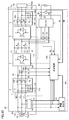
- FIG. 1 is a block diagram showing an overall configuration of an uninterruptible power supply U1 according to Embodiment 1 of the present invention.
- an uninterruptible power supply U1 is a three-phase four-wire system, and includes a switch 1, an AC input filter 2, a converter 3, an inverter 4, an AC output filter 5, and a DC / DC converter (“DC / DC 6, the control device 10, the DC lines L1 to L3, the neutral point line L4, the capacitors C1 and C2, the voltage detectors 31, 34, 35 and 36, the current detectors 32 and 37, and the power failure detector 33. Is provided.
- Switch 1 includes switches 1R, 1S, 1T. One terminals of the switches 1R, 1S, and 1T are connected to the R-phase terminal TR, the S-phase terminal TS, and the T-phase terminal TT of the three-phase four-wire commercial AC power supply 41, respectively, and supplied from the commercial AC power supply 41. R-phase voltage VR, S-phase voltage VS, and T-phase voltage VT are received, respectively. Neutral point terminal TN of commercial AC power supply 41 is connected to one end of neutral point line L4.
- the switches 1R, 1S, and 1T are controlled by the control device 10, and are turned on when three-phase AC power is normally supplied from the commercial AC power supply 41 (when the commercial AC power supply 41 is healthy). When the supply of three-phase AC power from the power supply is stopped (at the time of a power failure of the commercial AC power supply 41), it is turned off. The switches 1R, 1S, and 1T are turned off when the commercial AC power supply 41 fails, to electrically disconnect the commercial AC power supply 41 from the AC input filter 2.
- the AC input filter 2 is a three-phase LC filter circuit including a capacitor 11 (capacitors 11R, 11S, 11T) and a reactor 12 (reactors 12R, 12S, 12T).
- a capacitor 11 capacitor 11
- reactor 12 reactors 12R, 12S, 12T
- One electrodes of the capacitors 11R, 11S, and 11T are connected to the other terminals of the switches 1R, 1S, and 1T, respectively, and the other electrodes are connected to a neutral point line L4.
- One terminals of reactors 12R, 12S, 12T are connected to the other terminals of switches 1R, 1S, 1T, respectively, and the other terminals of reactors 12R, 12S, 12T are connected to three input nodes of converter 3, respectively.
- the AC input filter 2 is a low-pass filter that allows the commercial AC power supplied from the commercial AC power supply 41 to pass through the converter 3, and the switching frequency signal generated by the converter 3 is transmitted to the commercial AC power supply 41. Prevent passing.
- each of the DC lines L1 to L3 is connected to three output nodes of the converter 3, and the other end is connected to three input nodes of the inverter 4.
- DC line L2 is connected to neutral point line L4.
- the DC lines L1 to L3 are connected to three high-voltage nodes of the DC voltage converter 6.
- the DC lines L1 to L3 are converted to a positive voltage, a neutral point voltage, and a negative voltage by the converter 3 and the DC voltage converter 6, respectively.
- the capacitor C1 is connected between the DC lines L1 and L2, and smoothes and stabilizes the DC voltage Ep between the DC lines L1 and L2.
- Capacitor C2 is connected between DC lines L2 and L3, and smoothes and stabilizes DC voltage En between DC lines L2 and L3.
- Converter 3 is controlled by control device 10 and converts three-phase AC power supplied from commercial AC power supply 41 through AC input filter 2 to DC power when commercial AC power supply 41 is healthy, and converts the DC power to DC power.
- the power is supplied to the inverter 4 and the DC voltage converter 6 via the lines L1 to L3.
- the converter 3 is controlled so as to be zero.
- Control device 10 stops operation of converter 3 when DC voltage ⁇ E is smaller than threshold voltage ETH at the time of power failure of commercial AC power supply 41, so that DC voltage ⁇ E is lower than threshold voltage ETH. If it is larger, the converter 3 is controlled to reduce the DC voltage ⁇ E.
- the inverter 4 is controlled by the control device 10 and converts DC power from the converter 3 and the DC voltage converter 6 into three-phase AC power of a commercial frequency. As described later, converter 3, inverter 4, and DC voltage converter 6 each include a three-level circuit. The three-phase AC power generated by the inverter 4 is supplied to the load 42 via the AC output filter 5.
- the AC output filter 5 is a three-phase LC filter circuit composed of a reactor 18 (reactors 18U, 18V, 18W) and a capacitor 19 (capacitors 19U, 19V, 19W).
- Reactors 18U, 18V, and 18W have one terminals connected to three output nodes of inverter 4, respectively, and the other terminals connected to U-phase terminal TU, V-phase terminal TV, and W-phase terminal of three-phase four-wire load 42. Connected to TW.
- the AC output filter 5 is a low-pass filter that allows the commercial frequency three-phase AC power generated by the inverter 4 to pass through the load 42 and the switching frequency signal generated by the inverter 4 to pass through the load 42.
- the neutral terminal TNA of the load 42 is connected to the neutral line L4.
- the load 42 is driven by three-phase AC power supplied from the uninterruptible power supply U1.
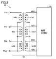
- FIG. 2 is a circuit block diagram illustrating the configuration of the load 42.
- the load 42 includes a three-phase four-wire transformer 43 and a three-phase four-wire load main body 46.
- Transformer 43 includes three primary windings 44U, 44V, 44W and three secondary windings 45U, 45V, 45W.
- One terminal of each of primary windings 44U, 44V, 44W is connected to U-phase terminal TU, V-phase terminal TV, and W-phase terminal TW of load 42, and the other terminal is connected to neutral point terminal TNA of load 42. Connected to.
- each of the secondary windings 45U, 45V, and 45W is connected to a U-phase terminal 46U, a V-phase terminal 46V, and a W-phase terminal 46W of the load main body 46, respectively. It is connected to the characteristic point terminal 46N.
- the three-phase AC voltage supplied from the uninterruptible power supply U1 is, for example, stepped down by the transformer 43 and supplied to the load main unit 46 to drive the load main unit 46.
- a battery B1 (power storage device) is connected between two low-voltage nodes of the DC voltage converter 6.
- DC voltage converter 6 is controlled by control device 10, and stores DC power generated by converter 3 in battery B1 when commercial AC power supply 41 is healthy. At that time, the control device 10 controls the DC voltage converter 6 so that the terminal voltage VB of the battery B1 becomes the reference battery voltage VBr (second reference voltage).
- the DC voltage converter 6 is controlled by the control device 10 and supplies the DC power of the battery B1 to the inverter 4 via the DC lines L1 to L3 when the commercial AC power supply 41 fails.
- the voltage converter 6 is controlled.
- a capacitor for example, an electric double layer capacitor
- the battery B1 is installed outside the uninterruptible power supply U1, but the battery B1 may be built in the uninterruptible power supply U1.
- a DC power supply (for example, a fuel cell) may be connected instead of the battery B1.
- the commercial AC power supply 41 is healthy, the operation of the DC voltage converter 6 is stopped.
- the voltage detector 31 detects instantaneous values of the AC voltages VR, VS, VT at the other terminals of the switches 1R, 1S, 1T, and outputs a three-phase voltage signal indicating the three-phase AC voltages VR, VS, VT to the control device 10 and Output to the power failure detector 33.
- Current detector 32 detects instantaneous values of alternating currents IR, IS, and IT flowing into three input nodes of converter 3, and outputs a three-phase current signal indicating three-phase alternating currents IR, IS, and IT to control device 10. Output.
- the power failure detector 33 determines whether or not a power failure has occurred in the commercial AC power supply 41 based on the three-phase voltage signal from the voltage detector 31, and outputs a power failure signal PC indicating the determination result.
- the power failure signal PC is at the “L” level of the deactivation level.
- the power failure signal PC becomes the activation level “H” level.
- the power failure signal PC is provided to the control device 10.
- the voltage detector 34 detects the voltage Ep between the terminals of the capacitor C1, and outputs a signal indicating the detected voltage Ep to the control device 10.
- Voltage detector 35 detects voltage En between terminals of capacitor C2 and outputs a signal indicating detected voltage En to control device 10.
- Voltage detector 36 detects a voltage VB between terminals of battery B1 and outputs a signal indicating detected voltage VB to control device 10.
- the current detector 37 detects the current IB output from the battery B1, and outputs a signal indicating the detected current IB to the control device 10.
- the control device 10 controls the operation of the switch 1, the converter 3, the inverter 4, and the DC voltage converter 6.
- converter 3, inverter 4, and DC voltage converter 6 are configured by semiconductor switches including semiconductor switching elements.
- IGBT Insulated Gate Bipolar Transistor
- PWM Pulse Width Modulation
- the control device 10 receives the three-phase voltage signal from the voltage detector 31, the three-phase current signal from the current detector 32, the signal indicating the voltage Ep detected by the voltage detector 34, and the voltage En detected by the voltage detector 35.
- PWM control is executed upon receiving a signal indicating the power failure signal PC from the power failure detector 33, a signal indicating the voltage VB detected by the voltage detector 36, a signal indicating the current IB detected by the current detector 37, and the like.
- FIG. 3 is a circuit diagram showing a configuration of converter 3 and inverter 4 shown in FIG. 3,
- converter 3 includes an R-phase arm 3R, an S-phase arm 3S, and a T-phase arm 3T.
- Inverter 4 includes a U-phase arm 4U, a V-phase arm 4V, and a W-phase arm 4W.
- Each phase arm (3R, 3S, 3T) of converter 3 and each phase arm (4U, 4V, 4W) of inverter 4 are each configured as a three-level circuit and include four IGBT elements and six diodes.
- R-phase arm 3R includes IGBT elements Q1R to Q4R and diodes D1R to D6R.
- S-phase arm 3S includes IGBT elements Q1S to Q4S and diodes D1S to D6S.
- T-phase arm 3T includes IGBT elements Q1T to Q4T and diodes D1T to D6T.
- U-phase arm 4U includes IGBT elements Q1U to Q4U and diodes D1U to D6U.
- V-phase arm 4V includes IGBT elements Q1V to Q4V and diodes D1V to D6V.
- W-phase arm 4W includes IGBT elements Q1W to Q4W and diodes D1W to D6W.
- IGBT elements Q1x to Q4x are connected in series between DC lines L1 and L3.
- the diodes D1x to D4x are connected in anti-parallel to the IGBT elements Q1x to Q4x, respectively.
- Diode D5x is connected to a connection point of IGBT elements Q1x, Q2x and DC line L2.
- Diode D6x is connected to a connection point of IGBT elements Q3x, Q4x and DC line L2.
- the cathode of the diode D5x is connected to the connection point of the IGBT elements Q1x and Q2x, and the anode of the diode D5x is connected to the DC line L2.
- the anode of diode D6x is connected to the connection point of IGBT elements Q3x, Q4x, and the cathode of diode D6x is connected to DC line L2.
- the diodes D1x to D4x function as freewheel diodes, and the diodes D5x and D6x function as clamp diodes.
- Converter 3 includes three input nodes 3a to 3c.
- Input node 3a is connected to the other terminal of reactor 12R (FIG. 1) and to a connection point of IGBT elements Q2R, Q3R.
- Input node 3b is connected to the other terminal of reactor 12S (FIG. 1) and to a connection point of IGBT elements Q2S, Q3S.
- Input node 3c is connected to the other terminal of reactor 12T (FIG. 1) and to a connection point of IGBT elements Q2T, Q3T.
- Inverter 4 includes three output nodes 4a to 4c.
- Output node 4a is connected to a connection point of IGBT elements Q2U and Q3U, and is connected to one terminal of reactor 18U (FIG. 1).
- Output node 4b is connected to a connection point of IGBT elements Q2V and Q3V, and is connected to one terminal of reactor 18V (FIG. 1).
- Output node 4c is connected to a connection point of IGBT elements Q2W and Q3W, and is connected to one terminal of reactor 18W (FIG. 1).
- FIG. 4 is a circuit diagram showing a configuration of DC voltage converter 6 shown in FIG.
- DC voltage converter 6 includes a semiconductor switch 21 and a reactor 22.
- Semiconductor switch 21 is configured as a three-level circuit, and includes IGBT elements Q1D to Q4D connected in series between DC lines L1 and L3, and diodes D1D to D4D connected in antiparallel to IGBT elements Q1D to Q4D, respectively.
- Reactor 22 includes reactors 22P and 22N.
- Reactor 22P is connected between a connection point of IGBT elements Q1D and Q2D and a positive electrode of battery B1.
- Reactor 22N is connected between a connection point of IGBT elements Q3D and Q4D and a negative electrode of battery B1.
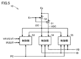
- FIG. 5 is a block diagram showing a portion related to control of converter 3 and DC voltage converter 6 in control device 10 (FIG. 1).
- control device 10 includes an adder 51, a subtractor 52, and control units 53 to 55.
- the subtractor 52 subtracts the voltage En between the terminals of the capacitor C2 detected by the voltage detector 35 from the voltage Ep between the terminals of the capacitor C1 detected by the voltage detector 34, and obtains the voltage Ep between the terminals of the capacitors C1 and C2.
- En, a DC voltage ⁇ E Ep ⁇ En.
- DC voltages VDC and ⁇ E are provided to each of control units 53 to 55.
- the control unit 53 receives the power failure signal PC from the power failure detector 33, the signals indicating the three-phase AC voltages VR, VS, and VT from the voltage detector 31, and the three-phase AC currents IR, IS, and IT from the current detector 32.
- the converter 3 is controlled based on a signal indicating the DC voltage VDC (first voltage) from the adder 51 and a signal indicating the DC voltage ⁇ E (second voltage) from the subtractor 52.
- control unit 53 determines the phase of three-phase AC voltages VR, VS, and VT.
- the converter 3 is controlled such that the phases of the three-phase AC currents IR, IS, and IT match, the DC voltage VDC becomes the reference DC voltage VDCr, and the DC voltage ⁇ E becomes 0.
- the control unit 53 determines whether the absolute value of the DC voltage ⁇ E is smaller than the threshold voltage ETH when the power failure signal PC is at the “H” level of the activation level (during a power failure of the commercial AC power supply 41). Stops the operation of the converter 3.
- control unit 53 determines that the absolute value of the DC voltage ⁇ E is greater than the threshold voltage ETH. Controls the converter 3 to reduce the DC voltage ⁇ E.
- the control units 54 and 55 include a power failure signal PC from the power failure detector 33, a signal representing the battery voltage VB from the voltage detector 36, a signal representing the DC current IB from the current detector 37, and a DC voltage from the adder 51.
- the DC voltage converter 6 is controlled based on the signal indicating VDC and the signal indicating the DC voltage ⁇ E from the subtractor 52.
- control unit 54 is activated when power failure signal PC is at the activation level “H” level (at the time of power failure of commercial AC power supply 41), and current IB at a level corresponding to battery voltage VB is generated.
- the DC voltage converter 6 is controlled such that the DC voltage VDC flows from the battery B1 to the capacitors C1 and C2, the DC voltage VDC becomes the reference DC voltage VDCr, and the DC voltage ⁇ E becomes 0.
- Control unit 55 is activated when power failure signal PC is at the “L” level of the deactivation level (when commercial AC power supply 41 is healthy), and current IB at a level corresponding to DC voltage VDC is applied to capacitors C1 and C2. To the battery B1, and controls the DC voltage converter 6 so that the battery voltage VB becomes the reference battery voltage VBr.
- FIG. 6 is a block diagram showing the configuration of the control unit 53 shown in FIG. 6, the control unit 53 includes a voltage command generation circuit 61, a balance control circuit 62, adders 63A to 63C, a determiner 64, and a PWM circuit 65.
- the voltage command generation circuit 61 includes a reference voltage generation circuit 81, subtractors 82 and 86A to 86C, a DC voltage control circuit 83, a sine wave generation circuit 84, multipliers 85A to 85C, a current control circuit 87, and adders 88A to 88C. including.
- the reference voltage generation circuit 81 generates a reference DC voltage VDCr.
- DC voltage control circuit 83 calculates a current command value I * for controlling the current flowing to the input side of converter 3 so that voltage ⁇ VDC becomes zero.
- DC voltage control circuit 83 calculates current command value I * by, for example, performing a proportional operation or a proportional integral operation on ⁇ VDC.
- the sine wave generation circuit 84 includes a sine wave signal having the same phase as the R phase voltage VR of the commercial AC power supply 41, a sine wave signal having the same phase as the S phase voltage VS of the commercial AC power supply 41, and a T phase voltage VT of the commercial AC power supply 41. And a sine wave signal having the same phase.
- the sine wave generation circuit 84 outputs a three-phase sine wave signal even when the commercial AC power supply 41 fails.
- the three sine wave signals are input to multipliers 85A to 85C, respectively, and are multiplied by current command value I * .
- current command values IR * , IS * , IT * having the same phase as the three-phase AC voltages VR, VS, VT of the commercial AC power supply 41 are generated.
- the subtractor 86A calculates a difference between the current command value IR * and the R-phase current IR detected by the current detector 32R.
- the subtractor 86B calculates the difference between the current command value IS * and the S-phase current IS detected by the current detector 32S.
- the subtractor 86C calculates the difference between the current command value IT * and the T-phase current IT detected by the current detector 32T.
- the current control circuit 87 determines which of the difference between the current command value IR * and the R-phase current IR, the difference between the current command value IS * and the S-phase current IS, and the difference between the current command value IT * and the T-phase current IT. Also, voltage command values VRa * , VSa * , and VTa * are generated as voltages to be applied to the reactor 12 so that also becomes zero.
- the current control circuit 87 generates a voltage command value by amplifying the difference between the current command value and the current value detected by the current detector according to proportional control or proportional integral control, for example.
- Adder 88A adds voltage command value VRa * and R-phase voltage VR detected by voltage detector 31 to generate voltage command value VR0 * .
- Adder 88B adds voltage command value VSa * and S-phase voltage VS detected by voltage detector 31 to generate voltage command value VS0 * .
- the adder 88C generates a voltage command value VT0 * by adding the T-phase voltage VT detected by the voltage command value VTa * and the voltage detector 31.
- the voltage command generation circuit 61 includes the three-phase AC voltages VR, VS, and VT detected by the voltage detector 31, the three-phase AC currents IR, IS, IT detected by the current detector 32, and the adder. 51 receives the DC voltage VDC calculated by, R-phase voltage command values each corresponding to S phase, and T phase VR0 *, VS0 *, generates a VT0 *.
- balance control circuit 62 generates voltage command value V1 * by performing a proportional operation or a proportional integral operation on ⁇ E.
- the voltage command is set so that the charging time of the capacitor C1 is shorter than the charging time of the capacitor C2.
- the value V1 * is generated.
- the voltage command is set so that the charging time of the capacitor C1 is longer than the charging time of the capacitor C2.
- the value V1 * is generated.
- the adder 63A generates a voltage command value VR * by adding the voltage command values VR0 * and V1 * .
- the adder 63B is the voltage command value VS0 *, generates a voltage command value VS * by adding V1 *.
- the adder 63C is the voltage command value VT0 *, generates a voltage command value VT * by adding V1 *.
- the determiner 64 generates a signal DT based on the power failure signal PC from the power failure detector 33 (FIG. 1) and the DC voltage ⁇ E from the subtractor 52 (FIG. 5).
- the signal DT is set to the "H" level of the activation level.
- the signal DT When the power failure signal PC is at the activation level “H” level (at the time of the commercial AC power supply 41 power failure) and the DC voltage ⁇ E is smaller than the threshold voltage ETH, the signal DT is at the inactivation level. It is set to the “L” level. When the power failure signal PC is at the activation level “H” level (at the time of the power failure of the commercial AC power supply 41) and the DC voltage ⁇ E is higher than the threshold voltage ETH, the signal DT has the activation level “ H "level.
- PWM circuit 65 is activated when signal DT is at the “H” level of the activation level, and detects three-phase AC detected by voltage detector 31 based on voltage command values VR * , VS * , and VT *.
- a signal is output to make the voltages VR, VS, and VT equal to the voltage command values VR * , VS * , and VT * , respectively.
- This signal is a signal for driving four IGBT elements included in each phase arm of converter 3.
- $ PWM circuit 65 is inactivated when signal DT is at the "L" level of the inactivation level, and turns off four IGBT elements included in each phase arm of converter 3. Thereby, the operation of converter 3 is stopped.
- the three-phase AC currents IR, IS, and IT have the same phase as the three-phase AC voltages VR, VS, and VT of the commercial AC power supply 41, and have a sine wave.
- the power factor can be made approximately 1.
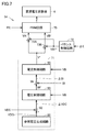
- FIG. 7 is a block diagram showing a configuration of the control unit 54 shown in FIG. 7, the control unit 54 includes a voltage command generation circuit 71, a balance control circuit 72, an adder 73A, a subtractor 73B, and a PWM circuit 75.
- Voltage command generation circuit 71 includes a reference voltage generation circuit 91, subtracters 92 and 94, a voltage control circuit 93, and a current control circuit 95.
- the reference voltage generation circuit 91 generates a reference DC voltage VDCr.
- the subtractor 92 calculates a voltage ⁇ VDC of a difference between the reference DC voltage VDCr and the DC voltage VDC detected by the adder 51 (FIG. 5).
- Voltage control circuit 93 calculates a current command value IB * at a level corresponding to voltage ⁇ VDC based on voltage VB between terminals of battery B1 detected by voltage detector 36 (FIG. 1).
- Voltage control circuit 93 calculates current command value IB * by, for example, performing a proportional operation or a proportional integral operation on ⁇ VDC.
- Current control circuit 95 generates voltage command value V * based on deviation ⁇ IB between current command value IB * and current value IB.
- the voltage command generation circuit 71 receives the battery voltage VB detected by the voltage detector 36, the battery current IB detected by the current detector 37, and the DC voltage VDC calculated by the adder 51, and A voltage command value V * for controlling the voltages Ep and En between the terminals C1 and C2 to a predetermined voltage is generated.
- balance control circuit 72 generates voltage command value VB1 * by performing a proportional operation or a proportional integral operation on DC voltage ⁇ E. For example, when ⁇ E> 0, the balance control circuit 72 sets the voltage command value VB1 * to a negative value. On the other hand, when ⁇ E ⁇ 0, the balance control circuit 72 sets the voltage command value VB1 * to a positive value.
- the adder 73A is * the voltage command value V, to generate a voltage command value VA * by adding VB1 *.
- the subtractor 73B generates a voltage command value VB * by subtracting the voltage command value VB1 * from the voltage command value V * .
- the voltage command values VA * and VB * are command values for controlling the voltages of the upper arm and the lower arm of the semiconductor switch 21, respectively.
- the voltage command values VA * and VB * of the voltages Ep and En for setting the difference .DELTA.E Command value.
- a command value generation circuit for generating the voltage command values VA * and VB * of the above.
- the PWM circuit 75 When the power failure signal PC is at the “H” level of the activation level (during a power failure of the commercial AC power supply 41), the PWM circuit 75 is activated and operates based on the voltage command values VA * and VB *. A signal for driving four IGBT elements included in 21 is output. The DC voltage converter 6 is controlled by a signal from the PWM circuit 75, and supplies DC power of the battery B1 to the inverter 4.
- the PWM circuit 75 When the power failure signal PC is at the “L” level of the deactivation level (when the commercial AC power supply 41 is healthy), the PWM circuit 75 is deactivated and does not perform the PWM control of the DC voltage converter 6. When commercial AC power supply 41 is healthy, DC voltage converter 6 is controlled by control unit 55 (FIG. 5), and stores DC power in battery B1.
- FIG. 8 is an equivalent circuit diagram showing a configuration for one phase of converter 3 shown in FIG.
- an R-phase arm 3R is shown as a switch 98 as an arm for one phase.
- Switch 98 includes a common terminal connected to input node 3a of converter 3, and three switching terminals connected to DC lines L1, L2, L3, respectively. In this switch 98, the common terminal and one of the three switching terminals are connected.
- the AC output in the inverter operation is in one of three potential states (p, c, n).
- p, c, and n are the voltages of the DC lines L1, L2, and L3, respectively.
- the voltages of the DC lines L1, L2, L3 are a positive voltage, a neutral point voltage, and a negative voltage, respectively.
- the neutral point voltage is, for example, a ground voltage (0 V).
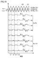
- FIG. 9 is a time chart showing the operation of control unit 53 shown in FIG. FIG. 9 shows PWM control of one phase (for example, R phase) of converter 3 (three-level PWM converter) when commercial AC power supply 41 is healthy.
- PWM control of one phase for example, R phase
- converter 3 three-level PWM converter
- voltage command signal 103 is a voltage command signal (VR0 * ) that has not been corrected by balance control circuit 62 (FIG. 6).
- the voltage command signal 103 is converted into a sine wave signal having the same phase as the R-phase voltage VR of the commercial AC power supply 41 by the sine wave generation circuit 84 (FIG. 6).
- the switching patterns of the four IGBT elements included in the R phase are determined by comparing the levels of the voltage command signal 103 and the reference signals 101 and 102. Is done. In this case, the switching patterns of IGBT elements Q1 to Q4 of the phase arm become switching patterns 111 to 114, and the output voltage of converter 3 becomes phase voltage 106.
- Each of the reference signals 101 and 102 is a triangular wave signal having a switching frequency sufficiently higher than the commercial frequency.
- the phase and the amplitude of the reference signal 101 match the phase and the amplitude of the reference signal 102.
- the reference signal 101 changes between 0V and the positive peak voltage.
- the reference signal 102 changes between the negative peak voltage and 0V.
- the amplitude of voltage command signal 103 is smaller than the sum of the amplitudes of reference signals 101 and 102.
- IGBT elements Q1 and Q2 are turned on, and IGBTs Q3 and Q4 are turned off.
- IGBT elements Q2 and Q3 are turned on and IGBTs Q1 and Q4 are turned off.
- IGBT elements Q3 and Q4 are turned on and IGBTs Q1 and Q2 are turned off.
- Voltage command signal 104 is a voltage command signal (VR * ) corrected by balance control circuit 62 when Ep ⁇ En, and is obtained by adding adjustment signal Vc1 to voltage command signal 103.
- the level of the voltage command signal 104 and the level of the reference signals 101 and 102 are compared to determine the switching patterns of the four IGBT elements included in the R phase (the same applies to the S and T phases). Is done. In this case, the switching patterns of IGBT elements Q1 to Q4 of the phase arm become switching patterns 121 to 124, and the output voltage of converter 3 becomes phase voltage 107.
- Voltage command signal 105 is a voltage command signal (VR * ) corrected by balance control circuit 62 when Ep> En, and is obtained by adding adjustment signal Vc2 to voltage command signal 103.
- the switching patterns of the four IGBT elements included in the R phase are determined by comparing the levels of the voltage command signal 105 and the reference signals 101 and 102. Is done. In this case, the switching patterns of IGBT elements Q1 to Q4 of the phase arm become switching patterns 131 to 134, and the output voltage of converter 3 becomes phase voltage 108.
- the voltage command signal 103 the voltage command value from voltage command generation circuit 61 (FIG. 6) (VR0 *, VS0 * , VT0 *) corresponding to each of the adjustment signals Vc1, Vc2 from balance control circuit 62 Corresponding to the voltage command value V1 * .
- Voltage command value V1 * is positive when Ep ⁇ En, and negative when Ep> En.
- FIG. 10 is another time chart showing the operation of control unit 53 shown in FIG. In FIG. 10, PWM control of one phase (for example, R phase) of converter 3 (three-level PWM converter) when the absolute value of ⁇ E exceeds threshold voltage ETH at the time of power failure of commercial AC power supply 41 is performed. It is shown.
- R phase for example, R phase
- ETH threshold voltage
- voltage command signal 103 is a voltage command signal (VR0 * ) that has not been corrected by balance control circuit 62 (FIG. 6).
- the voltage command signal 103 is converted into a sine wave signal having the same phase as the R-phase voltage VR of the commercial AC power supply 41 by the sine wave generation circuit 84 (FIG. 6).
- the switching patterns of the four IGBT elements included in the R phase are determined by comparing the levels of the voltage command signal 103 and the reference signals 101 and 102. Is done. In this case, the switching patterns of IGBT elements Q1 to Q4 of the phase arm become switching patterns 111 to 114, and the output voltage of converter 3 becomes phase voltage 106.
- Voltage command signal 104A is a voltage command signal (VR * ) corrected by balance control circuit 62 when Ep> En, and is obtained by adding adjustment signal Vc1 to voltage command signal 103.
- the switching patterns of the four IGBT elements included in the R phase are determined by comparing the levels of the voltage command signal 104A and the reference signals 101 and 102. Is done. In this case, the switching patterns of IGBT elements Q1 to Q4 of the phase arm become switching patterns 121A to 124A, and the output voltage of converter 3 becomes phase voltage 107A.
- Voltage command signal 105A is a voltage command signal (VR * ) corrected by balance control circuit 62 when Ep ⁇ En, and is obtained by adding adjustment signal Vc2 to voltage command signal 103.
- the switching patterns of the four IGBT elements included in the R phase are determined by comparing the levels of the voltage command signal 105A and the reference signals 101 and 102. Is done. In this case, the switching patterns of IGBT elements Q1 to Q4 of the phase arm become switching patterns 131A to 134A, and the output voltage of converter 3 becomes phase voltage 108A.
- the voltage command signal 103 the voltage command value from voltage command generation circuit 61 (FIG. 6) (VR0 *, VS0 * , VT0 *) corresponding to each of the adjustment signals Vc1, Vc2 from balance control circuit 62 Corresponding to the voltage command value V1 * .
- Voltage command value V1 * is positive when Ep> En, and negative when Ep ⁇ En.
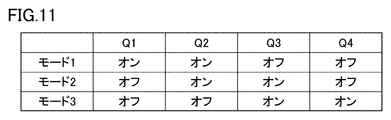
- FIG. 11 is a diagram showing switching patterns of four IGBT elements included in each phase arm of converter 3 shown in FIG.
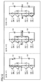
- FIGS. 12A to 12C are circuit diagrams showing the operation of each phase arm in each mode shown in FIG.
- FIG. 12A shows Mode 1. In mode 1, the IGBT elements Q1 and Q2 are turned on, and the positive-side smoothing capacitor C1 is charged (or discharged).
- FIG. 12B shows Mode 2. In mode 2, the IGBT elements Q2 and Q3 are turned on, and the power storage states of the positive-side smoothing capacitor C1 and the negative-side smoothing capacitor C2 do not change much.
- FIG. 12C shows mode 3. In mode 3, IGBT elements Q3 and Q4 are turned on, and negative-side smoothing capacitor C2 is charged (or discharged).
- arrows indicate the direction of current flowing during charging. At the time of discharging, a current flows in the direction opposite to the arrow.
- the balance control circuit 62 adds the adjustment signal Vc1 to the voltage command signal 103 and balances the voltage command signal with the voltage command signal in order to balance the voltages of the smoothing capacitors C1 and C2. Adjust to 104.
- switching levels 121 to 124 of the IGBT elements Q1 to Q4 are obtained by comparing the levels of the voltage command signal 104 and the reference signals 101 and 102. During the period when the voltage command signal 104 is positive, the positive-side smoothing capacitor C1 is charged. During the period when the voltage command signal 104 is negative, the negative-side smoothing capacitor C2 is charged.
- the charging period of the positive-side smoothing capacitor C1 is longer than the charging period of the negative-side smoothing capacitor C2.
- the balance control circuit 62 adds the adjustment signal Vc2 to the voltage command signal 103 and balances the voltage command signal with the voltage command in order to balance the voltages of the smoothing capacitors C1 and C2.
- the adjustment is made to become the signal 105.
- the switching patterns 131 to 134 of the IGBT elements Q1 to Q4 are obtained by comparing the levels of the voltage command signal 105 and the reference signals 101 and 102.
- the voltage command signal 104 While the voltage command signal 104 is positive, the positive-side smoothing capacitor C1 is charged. While the voltage command signal 104 is negative, the negative-side smoothing capacitor C2 is charged. Comparing the switching patterns without correction (111 to 114) and the switching patterns with correction (131 to 134), the charging period of the negative-side smoothing capacitor C2 is longer than the charging period of the positive-side smoothing capacitor C1.
- the balance control circuit 62 adds the adjustment signal Vc1 to the voltage command signal 103 and balances the voltage command signal with the voltage command signal in order to balance the voltages of the smoothing capacitors C1 and C2. Adjust to 104A.
- the voltage command signal 104A and the reference signals 101 and 102 are compared in level to obtain switching patterns 121A to 124A of the IGBT elements Q1 to Q4.
- the positive side smoothing capacitor C1 is discharged.
- the negative-side smoothing capacitor C2 is discharged.
- the discharge period of the positive smoothing capacitor C1 is longer than the discharge period of the negative smoothing capacitor C2.
- the balance control circuit 62 adds the adjustment signal Vc2 to the voltage command signal 103 and balances the voltage command signal with the voltage command in order to balance the voltages of the smoothing capacitors C1 and C2.
- the adjustment is made so that the signal becomes 105A.
- the switching patterns 131A to 134A of the IGBT elements Q1 to Q4 are obtained by comparing the levels of the voltage command signal 105A and the reference signals 101 and 102.
- FIGS. 13 to 15 are equivalent circuit diagrams showing the operation of one phase of converter 3 when the absolute value of ⁇ E exceeds threshold voltage ETH when commercial AC power supply 41 fails.
- the R-phase arm 3R is shown as an arm for one phase, and the R-phase arm 3R is shown as a switch 98.
- FIGS. 13 to 15 show the operation of one phase of converter 3 in modes 1 to 3 (FIGS. 11 and 12), respectively.
- the switch 1R is turned off, and the commercial AC power supply 41 is electrically disconnected from the capacitor 11R and the reactor 12R of the AC input filter 2. While the voltage command signal 103 is positive, the mode 1 and the mode 2 are executed alternately.
- the switch 98 (R-phase arm 3R) connects the DC line L1 to the input node 3a, and connects the DC line L1, the switch 98 (R-phase arm 3R) from the positive electrode of the capacitor C1.
- a current flows to the negative electrode of the capacitor C1 via the input node 3a, the reactor 12R, the capacitor 11R, and the neutral point line L4. Since the capacitance value of the capacitor C1 is sufficiently larger than the capacitance value of the capacitor 11R, the terminal voltage Ep of the capacitor C1 slightly decreases.
- the switch 98 (R-phase arm 3R) connects the DC line L2 to the input node 3a, and connects the reactor 12R, the input node 3a, and the switch 98 (R-phase) from one electrode of the capacitor 11R.
- a current flows to the other electrode of the capacitor 11R via the arm 3R), the DC line L2, and the neutral point line L4, and the terminal voltage of the capacitor 11R is reset to 0V. Therefore, when the voltage command signal 104A is positive, the mode 1 and the mode 2 are alternately performed, the capacitor C1 is discharged, and the terminal voltage Ep of the capacitor C1 gradually decreases.
- the switch 98 (R-phase arm 3R) connects the DC line L3 to the input node 3a, and connects the positive electrode of the capacitor C2 to the neutral point line L4, the capacitor 11R, the reactor 12R, and the input.
- a current flows to the negative electrode of the capacitor C2 via the node 3a, the switch (R-phase arm 3R), and the DC line L3. Since the capacitance value of the capacitor C2 is sufficiently larger than the capacitance value of the capacitor 11R, the terminal voltage En of the capacitor C2 slightly decreases.
- the DC line L2 and the input node 3a are connected by the switch 98 (R-phase arm 3R), and the voltage between the terminals of the capacitor 11R is reset to 0V. Therefore, when the voltage command signal 104A is negative, the mode 3 and the mode 2 are alternately performed to discharge the capacitor C2, and the terminal voltage En of the capacitor C2 gradually decreases.
- the time during which the mode 3 is executed (the discharge time of the capacitor C2) is the time during which the mode 1 is executed (the time during which the capacitor C1 is discharged). Since the discharge time is longer than the discharge time), En falls faster than Ep.
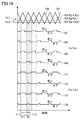
- FIG. 16 is a time chart showing the operation of control unit 54 shown in FIG.
- voltage command signal 154 is a voltage command signal (V * ) that has not been corrected by balance control circuit 72 (FIG. 7).
- the balance control circuit 72 changes the voltage command signal (VA * ) of the IGBT elements Q1D and Q3D to the voltage command signal 153 by adding the adjustment signal Vc1 to the voltage command signal 154.
- the balance control circuit 72 changes the voltage command signal (VB * ) of the IGBT elements Q2D and Q4D to the corrected voltage command signal 155 by subtracting the adjustment signal Vc1 from the voltage command signal 154.
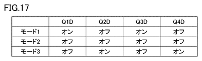
- FIG. 17 is a diagram showing a switching pattern of IGBT elements Q1D to Q4D shown in FIG.
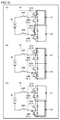
- FIGS. 18A to 18C are circuit diagrams showing the operation of the DC voltage converter 6 in the three modes shown in FIG.
- FIG. 18A shows mode 1.
- the IGBT elements Q1D and Q3D are turned on, and the positive-side smoothing capacitor C1 is charged.
- FIG. 18B shows mode 2.
- the IGBT elements Q1D to Q4D are turned off, and the power storage states of the positive-side smoothing capacitor C1 and the negative-side smoothing capacitor C2 do not change much.
- FIG. 18C shows mode 3.
- IGBT elements Q2D and Q4D are turned on, and negative-side smoothing capacitor C2 is charged.
- the PWM circuit 75 compares the voltage command signal 154 with the reference signal 151 to obtain the switching patterns 161 and 163 of the IGBT elements Q1 and Q3. Further, in the PWM circuit 75, the switching patterns 162 and 164 of the IGBT elements Q2 and Q4 are obtained by comparing the levels of the voltage command signal 154 and the reference signal 152.
- Both reference signals 151 and 152 are triangular wave signals.
- the frequency and amplitude of reference signal 151 are the same as the frequency and amplitude of reference signal 152.
- the phase of the reference signal 151 is shifted from the phase of the reference signal 152 by 180 degrees.
- IGBT elements Q1 and Q3 are turned on (mode 1).
- IGBT elements Q1 to Q4 are turned off (mode 2).
- IGBT elements Q2 and Q4 are turned on (mode 3).
- the IGBT elements Q1D to Q4D are operated in the mode 1, and the positive-side smoothing capacitor C1 is charged.
- IGBT elements Q1D to Q4D are operated in mode 3, and negative-side smoothing capacitor C2 is charged.
- the charging period (t11) of the positive-side smoothing capacitor C1 is longer than the charging period (t12) of the negative-side smoothing capacitor C2.
- FIG. 19 is another time chart showing the operation of control unit 54 shown in FIG.
- voltage command signal 154 is a voltage command signal (V * ) that has not been corrected by balance control circuit 72 (FIG. 7).
- the balance control circuit 72 changes the voltage command signal (VA * ) of the IGBT elements Q1D and Q3D to the voltage command signal 155 by adding the adjustment signal Vc1 to the voltage command signal 154. Further, balance control circuit 72 changes voltage command signal (VB * ) of IGBT elements Q2D, Q4D to corrected voltage command signal 153 by subtracting adjustment signal Vc1 from voltage command signal 154.
- the switching patterns 181 and 183 shown in FIG. 15 are obtained as the switching patterns of the IGBT elements Q1D and Q3D.
- the level of the voltage command signal 153 is compared with the level of the reference signal 152, so that the switching patterns 182 and 184 shown in FIG. 19 are obtained as the switching patterns of the IGBT elements Q2D and Q4D.
- the charging period (t11) of the positive-side smoothing capacitor C1 is longer than the charging period (t12) of the negative-side smoothing capacitor C2.
- the switch 1 When the commercial AC power supply 41 is healthy, the switch 1 is turned on, and three-phase AC power from the commercial AC power supply 41 is supplied to the converter 3 via the switch 1 and the AC input filter 2, and is converted into DC power by the converter 3. .
- the DC power is stored in the battery B1 by the DC voltage converter 6 and is converted into three-phase AC power by the inverter 4.
- the three-phase AC power generated by the inverter 4 is supplied to the load 42 via the AC output filter 5, and drives the load 42.
- the converter 3 is controlled by the control unit 53 (FIG. 6) so as to be 0.
- the switch 1 is turned off, the operation of the converter 3 is stopped, and the DC power of the battery B1 is supplied to the inverter 4 via the DC voltage converter 6, 4 converts it into three-phase AC power of the commercial frequency.
- the three-phase AC power generated by the inverter 4 is supplied to the load 42 via the AC output filter 5, and drives the load 42.
- the DC voltage converter 6 is controlled by the control unit 54 (FIG. 7) so as to be 0.
- the load 42 includes the three-phase four-wire transformer 43 and the load main body 46
- a three-phase excitation current flows through the transformer 43
- the uninterruptible power supply U 1 Each of the three-phase output currents has a positive / negative asymmetric waveform.
- the AC power supply, the uninterruptible power supply, the three-phase transformer, and the load main body are all of a three-phase three-wire type, the sum of the three-phase AC currents flowing through the three-phase transformer is zero, and thus the capacitor C1 , C2 are unlikely to become unbalanced.
- the commercial AC power supply 41, the uninterruptible power supply U1, the transformer 43, and the load main body 46 are of a three-phase four-wire type, and a current flows through the neutral point line L4.
- the sum of the three-phase AC currents flowing through the capacitor 43 does not become 0, and the voltages Ep and En between the terminals of the capacitors C1 and C2 may be unbalanced.
- the output current of the DC voltage converter 6 decreases, and the imbalance between the terminals Ep and En of the capacitors C1 and C2 can be eliminated. It may disappear.
- the voltage ⁇ E Ep ⁇ En of the difference between the voltages Ep and En between the terminals of the capacitors C1 and C2 exceeds a predetermined threshold voltage ETH.
- the converter 3 is started.
- the switch 1 when the commercial AC power supply 41 fails, the switch 1 is turned off to electrically disconnect the commercial AC power supply 41 from the AC input filter 2 and the voltage between the terminals of the capacitors C1 and C2.
- FIG. 20 is a circuit block diagram showing an overall configuration of an uninterruptible power supply U2 according to Embodiment 2 of the present invention, and is a diagram compared with FIG. Referring to FIG. 20, uninterruptible power supply U2 is different from uninterruptible power supply U1 in that voltage detector 31 is connected to one terminal of switch 1R, 1S, 1T (terminal on commercial AC power supply 41 side). The difference is that the instantaneous values of the voltages VR, VS, and VT are detected, and that the control device 10 is replaced by the control device 10A.
- the switch 1 When the commercial AC power supply 41 is healthy, the switch 1 is turned on, and the operation of the uninterruptible power supply U2 and the operation of the uninterruptible power supply U1 are the same.
- the voltage detector 31 detects the instantaneous values of the AC voltages VR, VS, VT appearing at one terminal of the switches 1R, 1S, 1T (terminals on the side of the commercial AC power supply 41). It is possible to easily and quickly detect that the AC power supply 41 has recovered from the power failure state to the healthy state.
- the voltage detector 31 detects the instantaneous values of the AC voltages VR, VS, and VT appearing at the other terminals (terminals on the side of the AC input filter 2) of the switches 1R, 1S, 1T. It is necessary to separately provide a means for detecting that the AC power supply 41 has recovered from the power failure state to the normal state.
- the voltage detector 31 detects the instantaneous values of the AC voltages VR, VS, VT appearing at one terminal of the switches 1R, 1S, 1T.
- the detection value of 31 may be incorrect and unstable, and the control unit 53 (FIG. 5) may malfunction.
- the control device 10 is replaced with a control device 10A.
- FIG. 21 is a circuit block diagram showing a main part of control device 10A, and is a diagram to be compared with FIG. Referring to FIG. 21, control device 10 ⁇ / b> A is obtained by adding a switching circuit 201 to control device 10.
- the switching circuit 201 indicates the AC voltages VR, VS, and VT detected by the voltage detector 31. The signal is given to the control unit 53.
- the switching circuit 201 When the power failure signal PC is at the “H” level of the activation level (during a power failure of the commercial AC power supply 41), the switching circuit 201 indicates the AC voltages VR, VS, and VT detected by the voltage detector 31. A signal indicating 0 V is supplied to the control unit 53 instead of the signal. Therefore, even when the commercial AC power supply 41 fails, the detection value of the voltage detector 31 becomes a constant value, so that a malfunction of the control unit 53 can be prevented.
- FIG. 22 is a circuit block diagram showing a modification of the second embodiment, and is a diagram to be compared with FIG. Referring to FIG. 22, in this modification, a control device 10B is provided instead of control device 10A.
- the control device 10B is obtained by adding a voltage estimation unit 202 to the control device 10A.
- Voltage estimating section 202 appears at the other terminal (terminal on the side of AC input filter 2) of switches 1R, 1S, 1T based on signals indicating three-phase AC currents IR, IS, IT detected by current detector 32.
- An instantaneous value of the three-phase AC voltage is estimated, and a signal indicating the estimated value is output.
- the voltage estimation unit 202 estimates the three-phase AC voltage by integrating the three-phase AC currents IR, IS, and IT detected by the current detector 32.
- the switching circuit 201 When the power failure signal PC is at the “L” level of the deactivation level (when the commercial AC power supply 41 is sound), the switching circuit 201 indicates the AC voltages VR, VS, and VT detected by the voltage detector 31. The signal is given to the control unit 53. Further, when power failure signal PC is at the “H” level of the activation level (at the time of commercial AC power supply 41 power failure), switching circuit 201 outputs a signal indicating three-phase AC voltage from voltage estimation unit 202 to control unit 53. Give to. Therefore, even in this modified example, it is possible to prevent the malfunction of the control unit 53 from occurring when the commercial AC power supply 41 fails.
- FIG. 23 is a circuit diagram showing a main part of an uninterruptible power supply according to Embodiment 3 of the present invention, and is a diagram to be compared with FIG. Referring to FIG. 23, the third embodiment differs from the first embodiment in that each of arms 3R, 3S, 3T, 4U, 4V, and 4W is formed of a three-level circuit 205.
- Three-level circuit 205 includes IGBT elements Q11 to Q14 and diodes D11 to D14.
- IGBT element Q11 is connected to DC line L1, and the emitter is connected to node N1.
- the collectors of IGBT elements Q12 and Q13 are connected to each other, and their emitters are connected to node N1 and DC line L2, respectively.
- IGBT element Q14 has a collector connected to node N1 and an emitter connected to DC line L3. Diodes D11 to D14 are connected in anti-parallel to IGBT elements Q11 to Q14, respectively.
- node N1 corresponds to input node 3a of converter 3.
- node N1 corresponds to input node 3b of converter 3.
- node N1 corresponds to input node 3c of converter 3.
- node N1 corresponds to output node 4a of inverter 4.
- node N1 corresponds to output node 4b of inverter 4.
- node N1 corresponds to output node 4c of inverter 4.
- FIGS. 9 and 10 it can be seen that the switching pattern of the IGBT element of the phase arm is composed of three modes.
- FIG. 24 is a diagram showing switching patterns of the four IGBT elements Q11 to Q14 shown in FIG. 23, and is a diagram to be compared with FIG.
- FIGS. 25A to 25C are circuit diagrams showing the operation of each phase arm in each mode shown in FIG.
- FIG. 25A shows Mode 1. In mode 1, the IGBT elements Q11 and Q12 are turned on, and the positive side smoothing capacitor C1 is charged (or discharged).
- FIG. 25B shows Mode 2. In mode 2, the IGBT elements Q12 and Q13 are turned on, and the power storage states of the positive-side smoothing capacitor C1 and the negative-side smoothing capacitor C2 do not change much.
- FIG. 25C illustrates mode 3. In mode 3, IGBT elements Q13 and Q14 are turned on, and negative-side smoothing capacitor C2 is charged (or discharged).
- arrows indicate the direction of current flowing during charging. At the time of discharging, a current flows in the direction opposite to the arrow. Therefore, three-level circuit 205 is equivalent to switch 98 (FIG. 8).
- U1, U2 uninterruptible power supply, 1,98 switch 2 input filter, 3 converter, 3R R phase arm, 3S S phase arm, 3T T phase arm, 4 inverter, 4U U phase arm, 4V V phase arm, 4W W Phase arm, 5 ° output filter, 6 ° DC voltage converter, B1 storage battery, 10, 10A, 10B control device, 11, 11R, 11S, 11T, C1, C2, 19, 19U, 19V, 19W, capacitor, 12, 12R, 12S , 12T, 18, 18U, 18V, 18W, 22, 22N, 22P reactor, L1 to L3 DC line, L4 neutral point line, 21 semiconductor switch, 31, 34, 35, 36 voltage detector, 32, 32R, 32S , 32T, 37 current detector, 33 blackout detector, 41 commercial AC power supply, 42 negative , 43 transformer, 44U, 44V, 44W primary winding, 45U, 45V, 45W secondary winding, 46 load body, Q1R to Q4R, Q1S to Q4S, Q1T to Q
Landscapes
- Engineering & Computer Science (AREA)
- Power Engineering (AREA)
- Business, Economics & Management (AREA)
- Emergency Management (AREA)
- Inverter Devices (AREA)
- Dc-Dc Converters (AREA)
- Stand-By Power Supply Arrangements (AREA)
- Rectifiers (AREA)
Abstract
Description
図1は、この発明の実施の形態1による無停電電源装置U1の全体構成を示すブロック図である。図1において、無停電電源装置U1は、三相4線式であって、スイッチ1、交流入力フィルタ2、コンバータ3、インバータ4、交流出力フィルタ5、直流電圧変換器(図中「DC/DC」と示す)6、制御装置10、直流ラインL1~L3、中性点ラインL4、コンデンサC1,C2、電圧検出器31,34,35,36、電流検出器32,37、および停電検出器33を備える。
図20は、この発明の実施の形態2による無停電電源装置U2の全体構成を示す回路ブロック図であって、図1と対比される図である。図20を参照して、この無停電電源装置U2が無停電電源装置U1と異なる点は、電圧検出器31がスイッチ1R,1S,1Tの一方端子(商用交流電源41側の端子)に現れる交流電圧VR,VS,VTの瞬時値を検出する点と、制御装置10が制御装置10Aで置換されている点である。
図23は、この発明の実施の形態3による無停電電源装置の要部を示す回路図であって、図3と対比される図である。図23を参照して、実施の形態3が実施の形態1と異なる点は、アーム3R,3S,3T,4U,4V,4Wの各々が3レベル回路205で構成されている点である。3レベル回路205は、IGBT素子Q11~Q14およびダイオードD11~D14を含む。
Claims (9)
- 第1~第3の直流ラインと、
前記第1および第2の直流ライン間に接続された第1のコンデンサと、
前記第2および第3の直流ライン間に接続された第2のコンデンサと、
三相4線式の交流電源の中性点端子、前記第2の直流ライン、および三相4線式の負荷の中性点端子に接続される中性点ラインと、
前記交流電源の各相に対応して設けられ、一方端子が前記交流電源から供給される対応する相の交流電圧を受け、前記交流電源の健全時にはオンされ、前記交流電源の停電時にはオフされるスイッチと、
前記スイッチの他方端子と前記中性点ラインとの間に接続された第3のコンデンサ、および一方端子が前記スイッチの他方端子に接続されたリアクトルを含む交流入力フィルタと、
前記リアクトルの他方端子と前記第1~第3の直流ラインとの間に接続され、交流電圧と第1~第3の直流電圧とを相互に変換可能に構成された第1のマルチレベル回路を含み、前記交流電源の健全時に、前記交流電源からの交流電力を直流電力に変換して前記第1~第3の直流ラインに供給するコンバータと、
直流電力供給源と前記第1~第3の直流ラインとの間に接続され、前記直流電力供給源から供給される第4の直流電圧と前記第1~第3の直流電圧とを相互に変換可能に構成された第2のマルチレベル回路を含み、前記交流電源の停電時に、前記直流電力供給源からの直流電力を前記第1~第3の直流ラインに供給する直流電圧変換器と、
前記第1~第3の直流ラインと前記負荷との間に設けられ、前記第1~第3の直流電圧と交流電圧とを相互に変換可能に構成された第3のマルチレベル回路を含み、前記コンバータおよび前記直流電圧変換器から供給される直流電力を交流電力に変換して前記負荷に供給するインバータと、
それぞれ前記第1および第2のコンデンサの端子間電圧を検出する第1および第2の電圧検出器と、
前記第1および第2の電圧検出器の検出結果に基づき、前記第1および第2のコンデンサの端子間電圧の和である第1の電圧と前記第1および第2のコンデンサの端子間電圧の差である第2の電圧とを求める演算器と、
前記交流電源の健全時には、前記第1の電圧が第1の参照電圧になり、かつ前記第2の電圧がなくなるように前記コンバータを制御し、前記交流電源の停電時には、前記第2の電圧の絶対値が予め定められたしきい値電圧よりも小さい場合は前記コンバータを停止させ、前記第2の電圧の絶対値が前記予め定められたしきい値電圧よりも大きい場合は前記コンバータを制御して前記第2の電圧を低減させる第1の制御部と、
前記交流電源の停電時に、前記第1の電圧が前記第1の参照電圧になり、かつ前記第2の電圧がなくなるように前記直流電圧変換器を制御する第2の制御部とを備える、無停電電源装置。 - 前記第1の制御部は、
前記交流電源の健全時には、前記第1および第2のコンデンサの充電時間が変化するように前記コンバータを制御し、
前記交流電源の停電時において、前記第2の電圧の絶対値が前記予め定められたしきい値電圧よりも大きい場合には、前記第1および第2のコンデンサの放電時間が変化するように前記コンバータを制御する、請求項1に記載の無停電電源装置。 - さらに、前記交流電源から供給される交流電圧の瞬時値を検出する第3の電圧検出器と、
前記第3の電圧検出器の検出値に基づいて前記交流電源の停電が発生したか否かを判別し、前記交流電源の停電が発生した場合に停電信号を出力する停電検出器とを備え、
前記第1の制御部は、前記停電検出器から前記停電信号が出力され、かつ、前記第2の電圧の絶対値が前記予め定められたしきい値電圧よりも大きい場合に、前記コンバータを制御して前記第2の電圧を低減させる、請求項1に記載の無停電電源装置。 - さらに、前記コンバータに流入する交流電流の瞬時値を検出する電流検出器を備え、
前記第1の制御部は、
前記第1の参照電圧と前記第1の電圧との偏差に応じたレベルを有し、正弦波状に変化する電流指令値を生成する電圧制御回路と、
前記電流指令値と前記電流検出器の検出値との偏差に応じたレベルの第1の電圧指令値を生成する電流制御回路と、
前記第1の電圧指令値に前記第3の電圧検出器の検出値を加算して第2の電圧指令値を生成する第1の加算器と、
前記第2の電圧に応じたレベルの第3の電圧指令値を生成するバランス制御回路と、
前記第2の電圧指令値に前記第3の電圧指令値を加算して第4の電圧指令値を生成する第2の加算器と、
前記停電検出器から前記停電信号が出力されていない場合と、前記停電検出器から前記停電信号が出力され、かつ、前記第2の電圧の絶対値が前記予め定められたしきい値電圧よりも大きい場合とに活性化され、前記第4の電圧指令値に基づいて、前記コンバータを制御する制御信号を生成する制御信号発生回路とを含む、請求項3に記載の無停電電源装置。 - 前記バランス制御回路は、
前記停電検出器から前記停電信号が出力されていない場合には、前記第1および第2のコンデンサの充電時間が変化するように前記第3の電圧指令値を生成し、
前記停電検出器から前記停電信号が出力され、かつ前記第2の電圧の絶対値が前記予め定められたしきい値電圧よりも大きい場合には、前記第1および第2のコンデンサの放電時間が変化するように前記第3の電圧指令値を生成する、請求項4に記載の無停電電源装置。 - 前記第3の電圧検出器は、前記スイッチの他方端子に現れる交流電圧の瞬時値を検出する、請求項4に記載の無停電電源装置。
- 前記第3の電圧検出器は、前記スイッチの一方端子に現れる交流電圧の瞬時値を検出し、
さらに、前記第3の電圧検出器と前記第1の加算器との間に設けられ、前記停電検出器から前記停電信号が出力されていない場合には、前記第3の電圧検出器の検出値を前記第1の加算器に与え、前記停電検出器から前記停電信号が出力されている場合には、前記第3の電圧検出器の検出値の代わりに0Vを示す信号を前記第1の加算器に与える切換回路を備える、請求項4に記載の無停電電源装置。 - 前記第3の電圧検出器は、前記スイッチの一方端子に現れる交流電圧の瞬時値を検出し、
さらに、前記電流検出器の検出値に基づいて、前記スイッチの他方端子に現れる交流電圧の瞬時値を推測する電圧推測部と、
前記停電検出器から前記停電信号が出力されていない場合には、前記第3の電圧検出器の出力信号を前記第1の加算器に与え、前記停電検出器から前記停電信号が出力されている場合には、前記第3の電圧検出器の検出値の代わりに前記電圧推測部によって推測された交流電圧の瞬時値を前記第1の加算器に与える切換回路を備える、請求項4に記載の無停電電源装置。 - 前記直流電力供給源は、直流電力を貯蔵する電力貯蔵装置であり、
前記第2のマルチレベル回路は、前記電力貯蔵装置から供給される前記第4の直流電圧と前記第1~第3の直流電圧とを相互に変換可能に構成されており、
前記直流電圧変換器は、前記交流電源の健全時には、前記コンバータによって生成された直流電力を前記電力貯蔵装置に蓄え、前記交流電源の停電時には、前記電力貯蔵装置の直流電力を前記第1~第3の直流ラインに供給し、
さらに、前記電力貯蔵装置の端子間電圧を検出する第3の電圧検出器と、
前記交流電源の健全時に、前記第3の電圧検出器の検出値が第2の参照電圧になるように前記直流電圧変換器を制御する第3の制御部とを備える、請求項1に記載の無停電電源装置。
Priority Applications (5)
| Application Number | Priority Date | Filing Date | Title |
|---|---|---|---|
| PCT/JP2018/029200 WO2020026430A1 (ja) | 2018-08-03 | 2018-08-03 | 無停電電源装置 |
| US17/258,318 US11411427B2 (en) | 2018-08-03 | 2018-08-03 | Uninterruptible power supply apparatus |
| JP2020534012A JP6955635B2 (ja) | 2018-08-03 | 2018-08-03 | 無停電電源装置 |
| KR1020217002702A KR102566567B1 (ko) | 2018-08-03 | 2018-08-03 | 무정전 전원 장치 |
| CN201880096059.1A CN112514200B (zh) | 2018-08-03 | 2018-08-03 | 不间断电源装置 |
Applications Claiming Priority (1)
| Application Number | Priority Date | Filing Date | Title |
|---|---|---|---|
| PCT/JP2018/029200 WO2020026430A1 (ja) | 2018-08-03 | 2018-08-03 | 無停電電源装置 |
Publications (1)
| Publication Number | Publication Date |
|---|---|
| WO2020026430A1 true WO2020026430A1 (ja) | 2020-02-06 |
Family
ID=69231640
Family Applications (1)
| Application Number | Title | Priority Date | Filing Date |
|---|---|---|---|
| PCT/JP2018/029200 Ceased WO2020026430A1 (ja) | 2018-08-03 | 2018-08-03 | 無停電電源装置 |
Country Status (5)
| Country | Link |
|---|---|
| US (1) | US11411427B2 (ja) |
| JP (1) | JP6955635B2 (ja) |
| KR (1) | KR102566567B1 (ja) |
| CN (1) | CN112514200B (ja) |
| WO (1) | WO2020026430A1 (ja) |
Cited By (4)
| Publication number | Priority date | Publication date | Assignee | Title |
|---|---|---|---|---|
| WO2022190167A1 (ja) * | 2021-03-08 | 2022-09-15 | 三菱電機株式会社 | 無停電電源装置 |
| JP7387913B1 (ja) * | 2022-06-27 | 2023-11-28 | 東芝三菱電機産業システム株式会社 | 無停電電源装置 |
| JP7581567B1 (ja) * | 2023-10-18 | 2024-11-12 | 株式会社Tmeic | 電力変換装置 |
| US12483159B2 (en) | 2021-11-22 | 2025-11-25 | Huawei Technologies Co., Ltd. | Controller for controlling a balancer circuit |
Families Citing this family (6)
| Publication number | Priority date | Publication date | Assignee | Title |
|---|---|---|---|---|
| EP3883115A4 (en) * | 2018-11-14 | 2022-06-22 | Toshiba Mitsubishi-Electric Industrial Systems Corporation | CURRENT TRANSFORMING DEVICE |
| JP7381236B2 (ja) * | 2019-07-24 | 2023-11-15 | ファナック株式会社 | 電力変換装置及びその制御方法 |
| JP7214040B2 (ja) * | 2020-03-27 | 2023-01-27 | 三菱電機株式会社 | 3レベル電力変換装置及び直流電源部の中間電位の制御方法 |
| CN114069819A (zh) * | 2020-08-07 | 2022-02-18 | 台达电子工业股份有限公司 | 具有三阶层切换电路的转换装置及三阶层切换电路的操作方法 |
| CN115663989B (zh) * | 2022-10-20 | 2023-04-28 | 上海山源电子科技股份有限公司 | 市电逆变切换控制方法及电路 |
| KR102942535B1 (ko) | 2024-01-22 | 2026-03-23 | 주식회사 온누리이엔지 | 배전 선로의 불평형 전류 저감형 무정전 전원공급 장치 및 방법 |
Citations (4)
| Publication number | Priority date | Publication date | Assignee | Title |
|---|---|---|---|---|
| WO2005101634A1 (en) * | 2004-03-24 | 2005-10-27 | Eaton Power Quality Corporation | Power conversion apparatus with dc bus precharge circuits and methods of operation thereof |
| WO2010021052A1 (ja) * | 2008-08-22 | 2010-02-25 | 東芝三菱電機産業システム株式会社 | 電力変換装置 |
| WO2015185630A1 (en) * | 2014-06-03 | 2015-12-10 | Abb Technology Ag | Uninterruptible power supply system with precharge converter |
| EP3309927A1 (en) * | 2016-10-13 | 2018-04-18 | Schneider Electric IT Corporation | Dc-link bus balancer |
Family Cites Families (10)
| Publication number | Priority date | Publication date | Assignee | Title |
|---|---|---|---|---|
| JP2007151231A (ja) * | 2005-11-24 | 2007-06-14 | Toshiba Mitsubishi-Electric Industrial System Corp | 無停電電源装置 |
| JP5631445B2 (ja) | 2008-08-22 | 2014-11-26 | 東芝三菱電機産業システム株式会社 | 電力変換装置 |
| JP5085742B2 (ja) * | 2008-10-16 | 2012-11-28 | 東芝三菱電機産業システム株式会社 | 電力変換装置 |
| JP5561071B2 (ja) * | 2010-09-29 | 2014-07-30 | サンケン電気株式会社 | 無停電電源装置 |
| JP5986005B2 (ja) * | 2013-01-30 | 2016-09-06 | 東芝三菱電機産業システム株式会社 | 無停電電源装置 |
| JP6243552B2 (ja) * | 2014-11-27 | 2017-12-06 | 東芝三菱電機産業システム株式会社 | 無停電電源装置 |
| EP3240139A4 (en) * | 2014-12-25 | 2018-08-15 | Toshiba Mitsubishi-Electric Industrial Systems Corporation | Uninterruptible power supply device |
| WO2017094142A1 (ja) * | 2015-12-02 | 2017-06-08 | 東芝三菱電機産業システム株式会社 | 無停電電源装置 |
| JP6725647B2 (ja) * | 2016-04-14 | 2020-07-22 | 東芝三菱電機産業システム株式会社 | 無停電電源装置 |
| US11228258B2 (en) * | 2018-11-20 | 2022-01-18 | Toshiba Mitsubishi-Electric Industrial Systems Corporation | Uninterruptible power supply apparatus |
-
2018
- 2018-08-03 JP JP2020534012A patent/JP6955635B2/ja active Active
- 2018-08-03 WO PCT/JP2018/029200 patent/WO2020026430A1/ja not_active Ceased
- 2018-08-03 KR KR1020217002702A patent/KR102566567B1/ko active Active
- 2018-08-03 US US17/258,318 patent/US11411427B2/en active Active
- 2018-08-03 CN CN201880096059.1A patent/CN112514200B/zh active Active
Patent Citations (4)
| Publication number | Priority date | Publication date | Assignee | Title |
|---|---|---|---|---|
| WO2005101634A1 (en) * | 2004-03-24 | 2005-10-27 | Eaton Power Quality Corporation | Power conversion apparatus with dc bus precharge circuits and methods of operation thereof |
| WO2010021052A1 (ja) * | 2008-08-22 | 2010-02-25 | 東芝三菱電機産業システム株式会社 | 電力変換装置 |
| WO2015185630A1 (en) * | 2014-06-03 | 2015-12-10 | Abb Technology Ag | Uninterruptible power supply system with precharge converter |
| EP3309927A1 (en) * | 2016-10-13 | 2018-04-18 | Schneider Electric IT Corporation | Dc-link bus balancer |
Cited By (9)
| Publication number | Priority date | Publication date | Assignee | Title |
|---|---|---|---|---|
| WO2022190167A1 (ja) * | 2021-03-08 | 2022-09-15 | 三菱電機株式会社 | 無停電電源装置 |
| JPWO2022190167A1 (ja) * | 2021-03-08 | 2022-09-15 | ||
| JP7566129B2 (ja) | 2021-03-08 | 2024-10-11 | 三菱電機株式会社 | 無停電電源装置 |
| US12218545B2 (en) | 2021-03-08 | 2025-02-04 | Tmeic Corporation | Uninterruptible power supply |
| US12483159B2 (en) | 2021-11-22 | 2025-11-25 | Huawei Technologies Co., Ltd. | Controller for controlling a balancer circuit |
| JP7387913B1 (ja) * | 2022-06-27 | 2023-11-28 | 東芝三菱電機産業システム株式会社 | 無停電電源装置 |
| WO2024003991A1 (ja) * | 2022-06-27 | 2024-01-04 | 東芝三菱電機産業システム株式会社 | 無停電電源装置 |
| JP7581567B1 (ja) * | 2023-10-18 | 2024-11-12 | 株式会社Tmeic | 電力変換装置 |
| WO2025083812A1 (ja) * | 2023-10-18 | 2025-04-24 | 株式会社Tmeic | 電力変換装置 |
Also Published As
| Publication number | Publication date |
|---|---|
| US20210175742A1 (en) | 2021-06-10 |
| KR102566567B1 (ko) | 2023-08-11 |
| KR20210024132A (ko) | 2021-03-04 |
| JP6955635B2 (ja) | 2021-10-27 |
| JPWO2020026430A1 (ja) | 2021-01-07 |
| CN112514200A (zh) | 2021-03-16 |
| US11411427B2 (en) | 2022-08-09 |
| CN112514200B (zh) | 2024-04-26 |
Similar Documents
| Publication | Publication Date | Title |
|---|---|---|
| JP6955635B2 (ja) | 無停電電源装置 | |
| JP6571903B1 (ja) | 無停電電源装置 | |
| JP5085742B2 (ja) | 電力変換装置 | |
| JP5463289B2 (ja) | 電力変換装置 | |
| JP5248611B2 (ja) | 電力変換装置 | |
| JP5770929B2 (ja) | 電源装置 | |
| WO2010095241A1 (ja) | 電力変換装置 | |
| US11394295B2 (en) | Power supply apparatus | |
| JP5631445B2 (ja) | 電力変換装置 | |
| US11336114B2 (en) | Uninterruptible power supply apparatus | |
| US11196290B2 (en) | Uninterruptible power supply apparatus |
Legal Events
| Date | Code | Title | Description |
|---|---|---|---|
| 121 | Ep: the epo has been informed by wipo that ep was designated in this application |
Ref document number: 18928445 Country of ref document: EP Kind code of ref document: A1 |
|
| ENP | Entry into the national phase |
Ref document number: 2020534012 Country of ref document: JP Kind code of ref document: A |
|
| ENP | Entry into the national phase |
Ref document number: 20217002702 Country of ref document: KR Kind code of ref document: A |
|
| NENP | Non-entry into the national phase |
Ref country code: DE |
|
| 122 | Ep: pct application non-entry in european phase |
Ref document number: 18928445 Country of ref document: EP Kind code of ref document: A1 |