WO2020026331A1 - アンテナ装置及び通信装置 - Google Patents
アンテナ装置及び通信装置 Download PDFInfo
- Publication number
- WO2020026331A1 WO2020026331A1 PCT/JP2018/028582 JP2018028582W WO2020026331A1 WO 2020026331 A1 WO2020026331 A1 WO 2020026331A1 JP 2018028582 W JP2018028582 W JP 2018028582W WO 2020026331 A1 WO2020026331 A1 WO 2020026331A1
- Authority
- WO
- WIPO (PCT)
- Prior art keywords
- terminal
- power
- phase
- power supply
- degrees
- Prior art date
- Legal status (The legal status is an assumption and is not a legal conclusion. Google has not performed a legal analysis and makes no representation as to the accuracy of the status listed.)
- Ceased
Links
Images









Classifications
-
- H—ELECTRICITY
- H01—ELECTRIC ELEMENTS
- H01Q—ANTENNAS, i.e. RADIO AERIALS
- H01Q13/00—Waveguide horns or mouths; Slot antennas; Leaky-waveguide antennas; Equivalent structures causing radiation along the transmission path of a guided wave
- H01Q13/08—Radiating ends of two-conductor microwave transmission lines, e.g. of coaxial lines, of microstrip lines
-
- H—ELECTRICITY
- H01—ELECTRIC ELEMENTS
- H01Q—ANTENNAS, i.e. RADIO AERIALS
- H01Q9/00—Electrically-short antennas having dimensions not more than twice the operating wavelength and consisting of conductive active radiating elements
- H01Q9/04—Resonant antennas
Definitions
- the present invention relates to an antenna device in which an excitation element is provided on a plane of a dielectric, and a communication device including the antenna device.
- An antenna device for satellite communication includes a communication device mounted on a satellite existing in a high elevation direction (hereinafter, referred to as a “high elevation angle communication satellite”) if the directional direction is a high elevation direction such as a zenith direction. ) Can be realized.
- a satellite communication antenna device is a communication device mounted on a satellite that exists in a low elevation angle direction if the pointing direction is a low elevation angle direction in which the elevation angle is lower than the elevation angle in the high elevation angle direction. (Hereinafter, referred to as a “low-elevation angle communication satellite”).
- An antenna device having a patch antenna is known as an antenna device of an antenna type having a strong directivity in a high elevation direction.
- an antenna device including the patch antenna may not be able to realize wireless communication with a low-elevation angle communication satellite.
- the size of the patch antenna it is possible to obtain a wide radiation pattern as the radiation pattern of the patch antenna. If a radiation pattern with a wide coverage area is obtained, the antenna device can realize wireless communication with a high-elevation angle communication satellite and can realize wireless communication with a low-elevation angle communication satellite.
- the size of the patch antenna is reduced, the bandwidth of the electromagnetic wave that can be transmitted and received by the antenna device is narrowed, so that the usable frequency range of the electromagnetic wave is limited.
- Patent Document 1 discloses a patch antenna in which a ring-shaped parasitic electrode is arranged so as to surround a radiation electrode. Since the patch antenna has the parasitic electrode, the directivity in the zenith direction is reduced, but the directivity in the low elevation angle direction is improved.
- Patent Literature 1 can enhance the directivity in a low elevation angle direction without narrowing the band of usable electromagnetic waves.
- the directivity in the zenith direction is reduced, there has been a problem that wireless communication with a communication device mounted on a satellite existing in the zenith direction may not be realized.
- the present invention has been made to solve the above-described problem, and realizes wireless communication with both a high-elevation angle communication satellite and a low-elevation angle communication satellite without causing a narrowing of usable electromagnetic waves. It is an object of the present invention to obtain an antenna device and a communication device that can perform the communication.
- An antenna device includes a first plane having a first plane and a second plane opposite to the first plane, wherein the first and second planes are circular in shape.
- a second dielectric provided on a plane opposite to the plane on which the second conductor is connected, one end of which is connected to the excitation element, the other end of which is a feeding point, and which is not electrically in contact with the ground conductor;
- a feed pin passing through each of the first dielectric and the second dielectric, wherein the diameter of the first and second planes and the thickness of the first dielectric are each a beam of electromagnetic waves. It is determined based on each of the width and the bandwidth of the electromagnetic wave.
- the diameters of the first and second planes and the thickness of the first dielectric are determined based on the beam width of the electromagnetic wave and the bandwidth of the electromagnetic wave, respectively.
- an antenna device Therefore, the antenna device according to the present invention can realize wireless communication with both the high-elevation-angle communication satellite and the low-elevation-angle communication satellite without reducing the band of usable electromagnetic waves.
- FIG. 1A is a plan view showing the antenna device according to the first embodiment
- FIG. 1B is a cross-sectional view showing a cross section taken along line X-X ′ in FIG. 1A
- FIG. 2 is a configuration diagram showing an interface circuit 7 of the antenna device according to the first embodiment.
- FIG. 3 is an explanatory diagram showing a layout of the interface circuit 7 shown in FIG. 1 is a configuration diagram illustrating a communication device according to a first embodiment.
- FIG. 9 is an explanatory diagram showing a simulation result regarding the minimum absolute gain of the antenna device when the beam width of the electromagnetic wave is 140 degrees.
- FIG. 9 is an explanatory diagram showing a simulation result regarding the minimum operation gain of the antenna device when the beam width of the electromagnetic wave is 140 degrees.
- FIG. 9 is an explanatory diagram showing a simulation result regarding the minimum operation gain of the antenna device when the beam width of the electromagnetic wave is 140 degrees.
- FIG. 4 is an explanatory diagram showing radiation of an electromagnetic wave from an excitation element 2 and radiation of an electromagnetic wave from a first power supply pin 5a, a second power supply pin 5b, a third power supply pin 5c, and a fourth power supply pin 5d.
- FIG. 9 is an explanatory diagram showing a simulation result of a radiation pattern when the thickness t of the first dielectric 1 is 0.25 ⁇ g and the diameter ⁇ d is 2.7 ⁇ g.
- FIG. 9 is an explanatory diagram showing a simulation result of a radiation pattern when the thickness t of the first dielectric 1 is 0.35 ⁇ g and the diameter ⁇ d is 2.7 ⁇ g.
- FIG. 3 is an explanatory diagram showing a simulation result regarding an amplitude at which power is distributed from the interface circuit 7 shown in FIG.
- FIG. FIG. 5 is a configuration diagram showing another interface circuit 7 of the antenna device according to the first embodiment.
- FIG. 13 is an explanatory diagram showing a simulation result on an amplitude at which power is distributed from the interface circuit 7 shown in FIG. 12 to Ports (5) to (8).
- FIG. FIG. 5 is a configuration diagram showing another interface circuit 7 of the antenna device according to the first embodiment.
- FIG. 16 is an explanatory diagram showing a simulation result regarding an amplitude at which power is distributed to the ports (5) to (8) from the interface circuit 7 shown in FIG.
- FIG. 18A is a plan view showing another antenna device according to the first embodiment
- FIG. 18B is a sectional view showing a section taken along line X-X ′ in FIG. 18A.
- FIG. 5 is an explanatory diagram showing a layout of another interface circuit 7 of the antenna device according to the first embodiment.
- FIG. 20A is a plan view showing the antenna device according to the second embodiment, and FIG.
- FIG. 20B is a cross-sectional view showing a cross section taken along line X-X ′ in FIG. 20A.
- FIG. 9 is an explanatory diagram showing a simulation result regarding the minimum operation gain of the antenna device when the beam width of the electromagnetic wave is 140 degrees. Radiation of electromagnetic waves from the excitation element 2, radiation of electromagnetic waves from the first power supply pin 5 a, second power supply pin 5 b, third power supply pin 5 c, and fourth power supply pin 5 d, and radiation from the non-excitation ring 51 It is explanatory drawing which shows the radiation of an electromagnetic wave.
- FIG. 9 is an explanatory diagram showing a simulation result.
- FIG. 24A is a plan view showing the antenna device according to the third embodiment
- FIG. 24B is a cross-sectional view showing a cross section taken along line X-X ′ in FIG. 24A.
- FIG. 9 is an explanatory diagram showing a simulation result regarding the minimum operation gain of the antenna device when the beam width of the electromagnetic wave is 140 degrees.
- FIG. 1A is a plan view showing the antenna device according to the first embodiment
- FIG. 1B is a cross-sectional view showing a cross section XX ′ in FIG. 1A
- the first dielectric 1 has a first plane 1a and a second plane 1b opposite to the first plane 1a.
- Each shape in the first plane 1a and the second plane 1b is a circle having a diameter ⁇ d
- the diameter ⁇ d is a beam width of an electromagnetic wave radiated from or received by the excitation element 2 and a band of the electromagnetic wave. Determined based on each of the widths.
- the thickness of the first dielectric 1 is t.
- the thickness t of the first dielectric 1 is determined based on the beam width of the electromagnetic wave radiated from the excitation element 2 or received by the excitation element 2 and the bandwidth of the electromagnetic wave, respectively. I have.
- the excitation element 2 is provided on the first plane 1a of the first dielectric 1, and emits or receives an electromagnetic wave.
- the planar shape of the excitation element 2 is circular.
- the diameter of the excitation element 2 corresponds to the resonance frequency of the excitation element 2 and, for example, a length of a half wavelength at the resonance frequency is good. However, this is only an example, and the diameter of the excitation element 2 may be longer or shorter than a half wavelength at the resonance frequency.
- the ground conductor 3 is provided on a second plane 1 b of the first dielectric 1. However, the ground conductor 3 is provided in the first plane of the second plane so as not to contact the first power supply pin 5a, the second power supply pin 5b, the third power supply pin 5c, and the fourth power supply pin 5d.
- the power supply pin 5a, the second power supply pin 5b, the third power supply pin 5c, and the fourth power supply pin 5d are not provided around the portion penetrating the first dielectric 1.
- the plane shape of the ground conductor 3 is circular.
- the second dielectric 4 is provided on a plane opposite to the plane in contact with the second plane 1b among the two planes of the ground conductor 3.
- the planar shape of the second dielectric 4 is circular.
- the antenna device illustrated in FIG. 1 includes a first power supply pin 5a, a second power supply pin 5b, a third power supply pin 5c, and a fourth power supply pin 5d as a plurality of power supply pins.
- One end of each of the first power supply pin 5a, the second power supply pin 5b, the third power supply pin 5c, and the fourth power supply pin 5d is connected to the excitation element 2.
- One end of each of the first power supply pin 5a, the second power supply pin 5b, the third power supply pin 5c, and the fourth power supply pin 5d is rotationally symmetric.
- the other end of the first power supply pin 5a is a power supply point 6a
- the other end of the second power supply pin 5b is a power supply point 6b.
- FIG. 1 omits the illustration of the feeding points 6a and 6c.
- the first power supply pin 5a, the second power supply pin 5b, the third power supply pin 5c, and the fourth power supply pin 5d are electrically non-contacted with the ground conductor 3 while the first dielectric 1 and the second power supply pin 5d are in contact with each other. 2 penetrates each of the two dielectrics 4.
- the feeding points 6a, 6b, 6c, and 6d are not formed as physical components of the antenna device, but indicate positions of feeding pins to which power is supplied from the interface circuit 7.
- the interface circuit 7 is provided on a plane opposite to the plane in contact with the ground conductor 3 among the two planes of the second dielectric 4.
- the interface circuit 7 is connected to the other ends of the first power supply pin 5a, the second power supply pin 5b, the third power supply pin 5c, and the fourth power supply pin 5d.
- the interface circuit 7 supplies power having the same amplitude and a different phase to the other end of each of the first power supply pin 5a, the second power supply pin 5b, the third power supply pin 5c, and the fourth power supply pin 5d.
- the ground via 8 has one end connected to the ground conductor 3 and the other end connected to the interface circuit 7, and penetrates through the second dielectric 4.
- the antenna device shown in FIG. 1 shows a four-point feeding circularly polarized antenna, and one end of a first feeding pin 5a, a second feeding pin 5b, a third feeding pin 5c, and a fourth feeding pin 5d. Are arranged at rotationally symmetric positions.
- the antenna device shown in FIG. 1 shows a four-point feeding circularly polarized antenna. However, this is merely an example, and for example, a one-point-feed circularly polarized antenna or a two-point fed circularly polarized antenna may be used. However, in the antenna device in which one end of the feeding pin is not located at a rotationally symmetric position but at an asymmetric position, the gain deviation between different directions is larger than that of the antenna device shown in FIG.
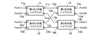
- FIG. 2 is a configuration diagram showing the interface circuit 7 of the antenna device according to the first embodiment
- FIG. 3 is an explanatory diagram showing a layout of the interface circuit 7 shown in FIG.
- the layout shown in FIG. 3 shows the layout when the direction of the interface circuit 7 is viewed from the excitation element 2.
- Port (1) is connected to a transmitting / receiving unit 21 described later.
- Port (1) uses the antenna apparatus shown in FIG. 1 to emit RHCP (right-handed circularly polarized) cross-polarized light in the zenith direction and radiate LHCP (left-handed circularly-polarized) cross-polarized light in the ground direction. When used as a circularly polarized antenna, this port is supplied with power from the transmission / reception unit 21.
- the zenith direction is a direction in which the elevation angle is about 90 degrees
- the ground direction is a direction in which the elevation angle is about 0 degrees.
- Port (3) is a port connected to the transmission / reception unit 21.
- Port (3) uses the antenna apparatus shown in FIG. 1 as a circularly polarized antenna that radiates cross polarization of LHCP in the zenith direction and radiates cross polarization of RHCP in the ground direction. This is the port to which power is applied.
- Port (3) When power is supplied from the transmission / reception unit 21 to Port (3), power is not supplied from the transmission / reception unit 21 to Port (1), Port (2), and Port (4).
- Port (2) and Port (4) are ports connected to the other end of the ground via 8.
- Port (5) is a port connected to a power supply point 6a, which is the other end of the first power supply pin 5a.
- Port (6) is connected to power supply point 6b, which is the other end of second power supply pin 5b.
- Port (7) is connected to power supply point 6c, which is the other end of third power supply pin 5c.
- Port (8) is connected to power supply point 6d, which is the other end of fourth power supply pin 5d.
- the first 180-degree hybrid 11 has a first terminal 11a, a second terminal 11b, a third terminal 11c, and a fourth terminal 11d.
- the first terminal 11a is connected to Port (1)
- the second terminal 11b is connected to Port (2).
- the third terminal 11c is connected to the first terminal 13a of the first 90-degree hybrid 13
- the fourth terminal 11d is connected to the first terminal 14a of the second 90-degree hybrid 14.
- the first 180-degree hybrid 11 outputs power having a phase of -90 degrees from the third terminal 11c when power is supplied from the transmission / reception unit 21 to the first terminal 11a via Port (1). Power having a phase of -270 degrees is output from the fourth terminal 11d.
- the power having a phase of ⁇ 90 degrees output from the third terminal 11 c is input to the first terminal 13 a of the first 90-degree hybrid 13.
- the power having a phase of -270 degrees output from the fourth terminal 11d is input to the first terminal 14a of the second 90-degree hybrid 14.
- the second 180-degree hybrid 12 has a first terminal 12a, a second terminal 12b, a third terminal 12c, and a fourth terminal 12d.
- the first terminal 12a is connected to Port (3)
- the second terminal 12b is connected to Port (4).
- the third terminal 12c is connected to the second terminal 13b of the first 90-degree hybrid 13
- the fourth terminal 12d is connected to the second terminal 14b of the second 90-degree hybrid 14.
- the second 180-degree hybrid 12 outputs power having a phase of -90 degrees from the third terminal 12c when power is supplied from the transmission / reception unit 21 to the first terminal 12a via Port (3). Power having a phase of -270 degrees is output from the fourth terminal 12d.
- the power having a phase of ⁇ 90 degrees output from the third terminal 12 c is input to the second terminal 13 b of the first 90-degree hybrid 13.
- the power having a phase of ⁇ 270 degrees output from the fourth terminal 12 d is input to the second terminal 14 b of the second 90-degree hybrid 14.
- the first 90-degree hybrid 13 has a first terminal 13a, a second terminal 13b, a third terminal 13c, and a fourth terminal 13d.
- the first terminal 13a is connected to the third terminal 11c of the first 180-degree hybrid 11, and the second terminal 13b is connected to the third terminal 12c of the second 180-degree hybrid 12.
- the third terminal 13c is connected to Port (5), and the fourth terminal 13d is connected to Port (6).
- the first 90-degree hybrid 13 receives power having a phase of ⁇ 90 degrees from the third terminal 11 c of the first 180-degree hybrid 11 to the first terminal 13 a, the phase from the third terminal 13 c becomes ⁇ .
- the power of 180 degrees is output, and the power of -270 degrees is output from the fourth terminal 13d.
- the power having a phase of -180 degrees output from the third terminal 13c is input to the feeding point 6a via Port (5).
- the power having a phase of -270 degrees output from the fourth terminal 12d is input to the feeding point 6b via the port (6).
- the first 90-degree hybrid 13 receives a power of ⁇ 90 degrees in phase from the third terminal 12 c of the second 180-degree hybrid 12 to the second terminal 13 b of the second 180-degree hybrid 12.
- the power of 270 degrees is output, and the power having a phase of -180 degrees is output from the fourth terminal 13d.
- the power having a phase of -270 degrees output from the third terminal 13c is input to the feeding point 6a via Port (5).
- the power having a phase of -180 degrees output from the fourth terminal 13d is input to the feeding point 6b via the port (6).
- the second 90-degree hybrid 14 has a first terminal 14a, a second terminal 14b, a third terminal 14c, and a fourth terminal 14d.
- the first terminal 14a is connected to the fourth terminal 11d of the first 180-degree hybrid 11, and the second terminal 14b is connected to the fourth terminal 12d of the second 180-degree hybrid 12.
- the third terminal 14c is connected to Port (7), and the fourth terminal 14d is connected to Port (8).
- the second 90-degree hybrid 14 When power having a phase of ⁇ 270 degrees is supplied from the fourth terminal 11d of the first 180-degree hybrid 11 to the first terminal 14a, the second 90-degree hybrid 14 has a phase of 0 from the third terminal 14c. And outputs power having a phase of -90 degrees from the fourth terminal 14d.
- the electric power having the phase of 0 degree output from the third terminal 14c is input to the feeding point 6c via Port (7).
- the power having a phase of -90 degrees output from the fourth terminal 14d is input to the feeding point 6d via Port (8).
- the second 90-degree hybrid 14 receives a ⁇ 270-degree phase power from the fourth terminal 12 d of the second 180-degree hybrid 12 to the second terminal 14 b of the second 180-degree hybrid 12.
- the power of 90 degrees is output, and the power of 0 degree is output from the fourth terminal 14d.
- the power having a phase of ⁇ 90 degrees output from the third terminal 14c is input to the feeding point 6c via Port (7).
- the power having a phase of 0 degrees output from the fourth terminal 14d is input to the feeding point 6d via Port (8).
- the layout shown in FIG. 3 includes a first 180-degree hybrid 11, a second 180-degree hybrid 12, a first 90-degree hybrid 13, and a second 90-degree hybrid 14 in order to reduce wasted power loss.
- 1 is an example of a layout in which the transmission line of the first embodiment is shortened.
- the transmission line connecting between the second 180-degree hybrid 12 and the first 90-degree hybrid 13 is formed by the first 90-degree hybrid 13 and the second 90-degree hybrid.
- the interface circuit 7 may be formed by patterning by etching or may be formed by chip components.
- FIG. 4 is a configuration diagram illustrating the communication device according to the first embodiment.
- the transmission / reception unit 21 is connected to the antenna device 22 via Port (1) and Port (3).
- the transmitting and receiving unit 21 radiates cross polarization of RHCP in the zenith direction, and when radiating cross polarization of LHCP in the ground direction, gives the power of the communication signal to Port (1).
- the transmitting and receiving unit 21 radiates LHCP cross-polarized light in the zenith direction, and applies RHCP cross-polarized light in the ground direction to supply power of the communication signal to Port (3).
- the transmission / reception unit 21 acquires the power of the communication signal from Port (1) or Port (3).
- the antenna device 22 is the antenna device illustrated in FIG. 1, and is connected to the transmission / reception unit 21 via Port (1) and Port (3).
- the transmission / reception unit 21 uses the first 180-degree hybrid via the port (1) to transmit the power of the communication signal. 11 to the first terminal 11a.
- the power of the communication signal is output from the transmission / reception unit 21 to the first terminal 11a of the first 180-degree hybrid 11 via Port (1), Port (2), Port (3) and Port (3) The isolation during 4) is ensured.
- the first 180-degree hybrid 11 When the power of the communication signal is supplied to the first terminal 11a, the first 180-degree hybrid 11 outputs power having a phase of -90 degrees from the third terminal 11c to the first terminal of the first 90-degree hybrid 13. 13a. Further, the first 180-degree hybrid 11 outputs power having a phase of ⁇ 270 degrees from the fourth terminal 11 d to the first terminal 14 a of the second 90-degree hybrid 14.
- the power of the communication signal is not supplied from the transmission / reception unit 21 to the Port (3). Therefore, no power is output from each of the third terminal 12c and the fourth terminal 12d of the second 180-degree hybrid 12.
- the phase from the third terminal 13 c becomes ⁇ .
- the power of 180 degrees is output to the feeding point 6a via Port (5).
- the first 90-degree hybrid 13 outputs power having a phase of -270 degrees from the fourth terminal 13d to the feeding point 6b via Port (6).
- the second 90-degree hybrid 14 has a phase of 0 from the third terminal 14c.
- the power is output to the feeding point 6c via the port (7).
- the second 90-degree hybrid 14 outputs power having a phase of -90 degrees from the fourth terminal 14d to the feeding point 6d via Port (8).
- the amplitudes of the powers supplied to the power supply points 6a, 6b, 6c, and 6d are the same, and the phases of the powers supplied to the power supply points 6a, 6b, and 6d are different from each other.
- the power having a phase of -180 degrees applied to the feeding point 6a is transmitted to one end of the first feeding pin 5a whose one end is located at the position of 6 o'clock in FIG. 1A.
- the power having a phase of -270 degrees applied to the feeding point 6b is transmitted to one end of the second feeding pin 5b whose one end is located at the 3 o'clock position in FIG. 1A.
- the electric power having a phase of 0 degree given to the feeding point 6c is transmitted to one end of the third feeding pin 5c whose one end is located at the 12 o'clock position in FIG. 1A.
- the power having a phase of ⁇ 90 degrees applied to the feeding point 6d is transmitted to one end of the fourth feeding pin 5d whose one end is located at the 9 o'clock position in FIG. 1A.
- the above-described power is transmitted to one end of each of the first power supply pin 5a, the second power supply pin 5b, the third power supply pin 5c, and the fourth power supply pin 5d, so that the excitation element 2 excites.
- the excitation element 2 excites, RHCP cross-polarized light is emitted from the excitation element 2 in the zenith direction, and LHCP cross-polarized light is emitted in the ground direction.
- the transmission / reception unit 21 When transmitting and receiving the cross polarization of LHCP in the zenith direction and the cross polarization of RHCP in the ground direction, the transmission / reception unit 21 transmits the power of the communication signal to the second 180-degree hybrid via Port (3). 12 to the first terminal 12a.
- the power of the communication signal is output from the transmission / reception unit 21 to the first terminal 12a of the second 180-degree hybrid 12 via Port (3), Port (1), Port (3), and Port (3) The isolation during 4) is ensured.
- the second 180-degree hybrid 12 When the power of the communication signal is supplied to the first terminal 12a, the second 180-degree hybrid 12 outputs power having a phase of -90 degrees from the third terminal 12c to the second terminal of the first 90-degree hybrid 13. 13b. Further, the second 180-degree hybrid 12 outputs power having a phase of ⁇ 270 degrees from the fourth terminal 12 d to the second terminal 14 b of the second 90-degree hybrid 14.
- the power of the communication signal is not supplied from the transmission / reception unit 21 to Port (1). Therefore, no power is output from each of the third terminal 11c and the fourth terminal 11d of the first 180-degree hybrid 11.
- the first 90-degree hybrid 13 receives a power of ⁇ 90 degrees in phase from the third terminal 12 c of the second 180-degree hybrid 12 to the second terminal 13 b of the second 180-degree hybrid 12.
- the power of 270 degrees is output to the feeding point 6a via Port (5).
- the first 90-degree hybrid 13 outputs power having a phase of -180 degrees from the fourth terminal 13d to the feeding point 6b via Port (6).
- the second 90-degree hybrid 14 receives a ⁇ 270-degree phase power from the fourth terminal 12 d of the second 180-degree hybrid 12 to the second terminal 14 b of the second 180-degree hybrid 12.
- the power of 90 degrees is output to the feeding point 6c via Port (7).
- the second 90-degree hybrid 14 outputs power having a phase of 0 degree from the fourth terminal 14d to the power supply point 6d via Port (8).
- the amplitudes of the powers supplied to the power supply points 6a, 6b, 6c, and 6d are the same, and the phases of the powers supplied to the power supply points 6a, 6b, and 6d are different from each other.
- the electric power having a phase of -270 degrees applied to the feeding point 6a is transmitted to one end of the first feeding pin 5a whose one end is located at the position of 6 o'clock in FIG. 1A.
- the power having a phase of -180 degrees applied to the feeding point 6b is transmitted to one end of the second feeding pin 5b whose one end is located at the 3 o'clock position in FIG. 1A.
- the power having a phase of -90 degrees applied to the feeding point 6c is transmitted to one end of the third feeding pin 5c whose one end is located at 12 o'clock in FIG. 1A.
- the power having a phase of 0 degree and given to the feeding point 6d is transmitted to one end of the fourth feeding pin 5d, which is arranged at one end at 9 o'clock in FIG. 1A.
- the above-described power is transmitted to one end of each of the first power supply pin 5a, the second power supply pin 5b, the third power supply pin 5c, and the fourth power supply pin 5d, so that the excitation element 2 excites.
- the excitation element 2 excites, a cross polarization of LHCP is emitted from the excitation element 2 in the zenith direction, and a cross polarization of RHCP is emitted in the ground direction.
- the transmission / reception unit 21 can switch the radiated polarization by switching between Port (1) and Port (3) as the output destination of the power of the communication signal.
- the antenna device illustrated in FIG. 1 is used as a circularly polarized antenna that radiates cross polarized waves.
- the antenna device shown in FIG. 1 can perform wireless communication with a high-elevation angle communication satellite and wireless communication with a low-elevation angle communication satellite
- the high-elevation angle communication satellite is a communication device mounted on a satellite existing in a high elevation angle direction
- the low-elevation angle communication satellite is a communication device mounted on a satellite existing in a low elevation angle direction. It is.
- the high elevation direction is, for example, the zenith direction
- the low elevation direction is, for example, a direction in which the elevation angle is 20 degrees.
- the coverage area of the antenna device must be high at an elevation angle of 20 degrees or more.
- the beam width of the electromagnetic wave in the antenna device is determined by the respective diameters ⁇ d in the first plane 1a and the second plane 1b. Further, the beam width of the electromagnetic wave in the antenna device is determined by the thickness t of the first dielectric 1.
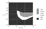
- FIG. 5 is an explanatory diagram showing a simulation result of the lowest absolute gain of the antenna device when the beam width of the electromagnetic wave is 140 degrees.
- FIG. 6 is an explanatory diagram showing a simulation result of the lowest operation gain of the antenna device when the beam width of the electromagnetic wave is 140 degrees.
- ⁇ g is the wavelength of the electromagnetic wave inside the first dielectric 1 at the center frequency of the electromagnetic wave. In the simulations in FIGS. 5 and 6, it is assumed that the relative permittivity of the first dielectric 1 is 3.62 and the dielectric loss tangent of the first dielectric 1 is 0.005.
- the thickness t is in the range of about 0.20 ⁇ g to about 0.28 ⁇ g and the diameter ⁇ d is in the range of about 2.4 ⁇ g to about 3.0 ⁇ g, in both the absolute gain and the operating gain, It can be seen that the gain is higher than 0 [dBi].
- the thickness t of the first dielectric 1 is a parameter that contributes to the coverage and also a parameter that contributes to the bandwidth. Therefore, when the thickness t of the first dielectric 1 is small, a wide band cannot be covered, and the mismatch loss increases. For example, when the thickness t is 0.15 ⁇ g, the mismatch loss increases, and the operation gain is smaller than 0 [dBi].
- the increase in the thickness t of the first dielectric 1 means that the lengths of the first power supply pin 5a, the second power supply pin 5b, the third power supply pin 5c, and the fourth power supply pin 5d become longer. Is equivalent to For example, when the thickness t of the first dielectric 1 is about 0.25 ⁇ g, as shown in FIG.
- the first feed pin 5a and the second Electromagnetic waves are radiated from the power supply pin 5b, the third power supply pin 5c, and the fourth power supply pin 5d.
- the radiation of electromagnetic waves from the first power supply pin 5a, the second power supply pin 5b, the third power supply pin 5c, and the fourth power supply pin 5d is radiation of electromagnetic waves as a monopole antenna.
- FIG. 7 is an illustration showing radiation of electromagnetic waves from the excitation element 2 and radiation of electromagnetic waves from the first power supply pin 5a, the second power supply pin 5b, the third power supply pin 5c, and the fourth power supply pin 5d.
- FIG. The addition of the radiation of the electromagnetic waves from the first power supply pin 5a, the second power supply pin 5b, the third power supply pin 5c, and the fourth power supply pin 5d increases the gain in the low elevation angle direction.
- the electromagnetic wave radiated from the antenna device 22 propagates as a surface wave near the first plane 1a of the first dielectric 1, so that the gain in the low elevation angle direction increases. I do. From the above, it can be seen that there is a thickness t and a diameter ⁇ d that enable wireless communication with a high elevation angle communication satellite and wireless communication with a low elevation angle communication satellite.
- FIG. 8 is an explanatory diagram showing a simulation result of a radiation pattern when the thickness t of the first dielectric 1 is 0.25 ⁇ g and the diameter ⁇ d is 2.7 ⁇ g.
- the simulation results shown in FIG. 8 indicate that the zenith angle ⁇ has a high gain of 0 [dBi] or more in the range of ⁇ 75 [deg] ⁇ ⁇ +75 [deg].
- FIG. 9 is an explanatory diagram showing a simulation result of a radiation pattern when the thickness t of the first dielectric 1 is 0.35 ⁇ g and the diameter ⁇ d is 2.7 ⁇ g. In the simulation in FIG.
- the thickness t of the first dielectric 1 is larger than in the simulation in FIG.
- the diameter ⁇ d is the same.
- the gain near the zenith angle ⁇ of ⁇ 50 [deg] tends to increase, and the gain near the zenith angle ⁇ of ⁇ 20 [deg] tends to decrease.
- This tendency is that, as the thickness t increases, the distance between the excitation element 2 and the ground conductor 3 increases, and the strength of the magnetic current generated between the excitation element 2 and the ground conductor 3 decreases. Radiation of electromagnetic waves in the zenith direction is reduced.
- the intensity of the current flowing through the first power supply pin 5a, the second power supply pin 5b, the third power supply pin 5c, and the fourth power supply pin 5d becomes greater than the intensity of the magnetic current. It is considered that the radiation of the electromagnetic wave from the power supply pin 5a and the like became dominant, and the radiation of the electromagnetic wave was increased near the zenith angle ⁇ of ⁇ 50 [deg].
- FIG. 10 is an explanatory diagram showing a simulation result regarding the amplitude at which power is distributed from the interface circuit 7 to the ports (5) to (8) shown in FIG.
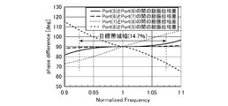
- FIG. 11 shows that when power is distributed from the interface circuit 7 shown in FIG. 2 to Ports (5) to (8), the excitation phase difference between adjacent ports in Ports (5) to (8) is reduced.
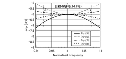
- FIG. 9 is an explanatory diagram showing a simulation result. 10 and 11, it is assumed that the target bandwidth, which is a desired frequency range of the electromagnetic wave, is 14.7%. In the simulations of FIG. 10 and FIG. 11, crawling of the transmission line between the first 180-degree hybrid 11, the second 180-degree hybrid 12, the first 90-degree hybrid 13, and the second 90-degree hybrid 14 Not considered.
- the dimensions of the first 180-degree hybrid 11, the second 180-degree hybrid 12, the first 90-degree hybrid 13, and the second 90-degree hybrid 14 are determined by the center frequency of the electromagnetic wave. It is also assumed that the relative permittivity of the second dielectric 4 on which the interface circuit 7 is formed is 3.62, and the dielectric loss tangent of the second dielectric 4 is 0.005. When the target bandwidth is 14.7%, as shown in FIG. 10, the amplitude variation at the band edge is 0.58 [dB]. When the target bandwidth is 14.7%, as shown in FIG. 11, the excitation phase difference between adjacent ports is 0.4 [deg].
- the interface circuit 7 shown in FIG. 2 includes two 180-degree hybrids and two 90-degree hybrids.
- the interface circuit 7 shown in FIG. 2 may include four 90-degree hybrids as shown in FIG.
- FIG. 12 is a configuration diagram showing another interface circuit 7 of the antenna device according to the first embodiment.
- the 90-degree hybrid 31 has a first terminal 31a, a second terminal 31b, a third terminal 31c, and a fourth terminal 31d.
- the first terminal 31a is connected to Port (1)
- the second terminal 31b is connected to Port (2).
- the third terminal 31c is connected to the first terminal 33a of the 90-degree hybrid 33
- the fourth terminal 31d is connected to the second terminal 34b of the 90-degree hybrid 34.
- the 90-degree hybrid 31 When power is applied to the first terminal 31a from the transmission / reception unit 21 via Port (1), the 90-degree hybrid 31 outputs power having a phase of ⁇ 90 degrees from the third terminal 31c, and outputs the fourth power. Power having a phase of -180 degrees is output from the terminal 31d. The power having a phase of ⁇ 90 degrees output from the third terminal 31 c is input to the first terminal 33 a of the 90-degree hybrid 33. The power having a phase of ⁇ 180 degrees output from the fourth terminal 31 d is input to the second terminal 34 b of the 90-degree hybrid 34.
- the 90-degree hybrid 32 has a first terminal 32a, a second terminal 32b, a third terminal 32c, and a fourth terminal 32d.
- the first terminal 32a is connected to Port (3)
- the second terminal 32b is connected to Port (4).
- the third terminal 32c is connected to the first terminal 34a of the 90-degree hybrid 34
- the fourth terminal 32d is connected to the second terminal 33b of the 90-degree hybrid 33.
- the power having a phase of ⁇ 90 degrees output from the third terminal 32 c is input to the first terminal 34 a of the 90-degree hybrid 34.
- the power having a phase of ⁇ 180 degrees output from the fourth terminal 32 d is input to the second terminal 33 b of the 90-degree hybrid 33.
- the 90-degree hybrid 33 has a first terminal 33a, a second terminal 33b, a third terminal 33c, and a fourth terminal 33d.
- the first terminal 33a is connected to the third terminal 31c of the 90-degree hybrid 31, and the second terminal 33b is connected to the fourth terminal 32d of the 90-degree hybrid 32.
- the third terminal 33c is connected to Port (5), and the fourth terminal 33d is connected to Port (6).
- the 90-degree hybrid 33 outputs power having a phase of -180 degrees from the third terminal 33c when power of -90 degrees is supplied from the third terminal 31c of the 90-degree hybrid 31 to the first terminal 33a. At the same time, power having a phase of -270 degrees is output from the fourth terminal 33d.
- the power having a phase of -180 degrees output from the third terminal 33c is input to the feeding point 6a via Port (5).
- the power having a phase of -270 degrees output from the fourth terminal 33d is input to the feeding point 6b via Port (6).
- the 90-degree hybrid 33 outputs power having a phase of 0 degree from the third terminal 33c when power having a phase of -180 degrees is supplied from the fourth terminal 32d of the 90-degree hybrid 32 to the second terminal 33b.
- power having a phase of -270 degrees is output from the fourth terminal 33d.
- the power having the phase of 0 degree output from the third terminal 33c is input to the power supply point 6a via Port (5).
- the power having a phase of -270 degrees output from the fourth terminal 33d is input to the feeding point 6b via Port (6).
- the 90-degree hybrid 34 has a first terminal 34a, a second terminal 34b, a third terminal 34c, and a fourth terminal 34d.
- the first terminal 34a is connected to the third terminal 32c of the 90-degree hybrid 32
- the second terminal 34b is connected to the fourth terminal 31d of the 90-degree hybrid 31.
- the third terminal 34c is connected to Port (7)
- the fourth terminal 34d is connected to one end of the 180-degree delay line 35.
- the 90-degree hybrid 34 outputs power having a phase of 0 degree from the third terminal 34c when power having a phase of -180 degrees is supplied from the fourth terminal 31d to the second terminal 34b of the 90-degree hybrid 31. At the same time, power having a phase of -270 degrees is output from the fourth terminal 14d.
- the power having the phase of 0 degree output from the third terminal 34c is input to the feeding point 6c via Port (7).
- the power having a phase of -270 degrees output from the fourth terminal 34d is input to one end of the 180-degree delay line 35.
- the 90-degree hybrid 34 outputs power having a phase of -180 degrees from the third terminal 34c when power of -90 degrees is supplied from the third terminal 32c of the 90-degree hybrid 32 to the first terminal 34a.
- power having a phase of -270 degrees is output from the fourth terminal 34d.
- the power having a phase of -180 degrees output from the third terminal 34c is input to the feeding point 6c via Port (7).
- the power having a phase of -270 degrees output from the fourth terminal 34d is input to one end of the 180-degree delay line 35.
- One end of the 180-degree delay line 35 is connected to the fourth terminal 34d of the 90-degree hybrid 34, and the other end is connected to Port (8).
- the 180-degree delay line 35 delays the phase of the power output from the fourth terminal 34d of the 90-degree hybrid 34 by 180 degrees and supplies power to the first terminal 31a via Port (1).
- power having a phase of -90 degrees is output to the port (8).
- FIG. 13 is an explanatory diagram showing a simulation result on the amplitude at which power is distributed from the interface circuit 7 to the ports (5) to (8) shown in FIG.
- FIG. 14 is a graph showing the excitation phase difference between adjacent ports in Ports (5) to (8) when power is distributed to Ports (5) to (8) from the interface circuit 7 shown in FIG.
- FIG. 9 is an explanatory diagram showing a simulation result. 13 and 14, it is assumed that the target bandwidth is 14.7%, as in FIGS. In the simulations of FIGS. 13 and 14, crawling of the transmission line between the 90-degree hybrid 31, the 90-degree hybrid 32, the 90-degree hybrid 33, and the 90-degree hybrid 34 is not considered. The dimensions of the 90-degree hybrids 31 to 34 are determined by the center frequency of the electromagnetic wave. It is also assumed that the relative permittivity of the second dielectric 4 on which the interface circuit 7 is formed is 3.62, and the dielectric loss tangent of the second dielectric 4 is 0.005.
- the amplitude variation at the band edge is 1.24 [dB], and the characteristics are worse than the interface circuit 7 shown in FIG. I have.
- the excitation phase difference between adjacent ports is 16.6 [deg], which is smaller than that of the interface circuit 7 shown in FIG. , The characteristics are getting worse.
- One of the causes of the deterioration of the characteristics is that the 90-degree hybrids 31 and 32 have an amplitude at the band edge more than the first 180-degree hybrid 11 and the second 180-degree hybrid 12 because the fractional band is about 10%. It is considered that the characteristics are deteriorated.
- the phase inclination of Port (8) becomes steeper than that of Ports (5) to (7) because the 180-degree delay line 35 is connected. It is thought that it is. This is because, because of the steep phase gradient, good characteristics can be obtained at the center frequency, but the phase characteristics deteriorate significantly as the distance from the center frequency increases.
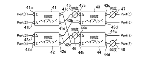
- the interface circuit 7 shown in FIG. 2 may include four 180-degree hybrids as shown in FIG.
- FIG. 15 is a configuration diagram showing another interface circuit 7 of the antenna device according to the first embodiment.
- the 180-degree hybrid 41 has a first terminal 41a, a second terminal 41b, a third terminal 41c, and a fourth terminal 41d.
- the first terminal 41a is connected to Port (1)
- the second terminal 41b is connected to Port (2).
- the third terminal 41c is connected to the second terminal 44b of the 90-degree hybrid 44
- the fourth terminal 41d is connected to one end of the 90-degree delay line 45.
- the 180-degree hybrid 41 When power is applied to the first terminal 41a from the transmission / reception unit 21 via Port (1), the 180-degree hybrid 41 outputs power having a phase of ⁇ 90 degrees from the third terminal 41c and outputs the fourth power. Power having a phase of -270 degrees is output from the terminal 41d. The power output from the third terminal 41 c and having a phase of ⁇ 90 degrees is input to the second terminal 44 b of the 90-degree hybrid 44. The power having a phase of ⁇ 270 degrees output from the fourth terminal 41 d is input to the 90-degree delay line 45.
- the 180-degree hybrid 42 has a first terminal 42a, a second terminal 42b, a third terminal 42c, and a fourth terminal 42d.
- the first terminal 42a is connected to Port (3)
- the second terminal 42b is connected to Port (4).
- the third terminal 42c is connected to the second terminal 43b of the 90-degree hybrid 43
- the fourth terminal 42d is connected to one end of the 90-degree delay line 46.
- the power having a phase of ⁇ 90 degrees output from the third terminal 42 c is input to the second terminal 43 b of the 90-degree hybrid 43.
- the power having a phase of ⁇ 90 ° output from the fourth terminal 42d is input to the 90 ° delay line 46.
- One end of the 90-degree delay line 45 is connected to the fourth terminal 41 d of the 180-degree hybrid 41, and the other end is connected to the first terminal 43 a of the 180-degree hybrid 43.
- the 90-degree delay line 45 delays the phase of the power output from the fourth terminal 41 d of the 180-degree hybrid 41 by 90 degrees and outputs the power after the phase delay to the first terminal 43 a of the 180-degree hybrid 43.
- One end of the 90-degree delay line 46 is connected to the fourth terminal 42 d of the 180-degree hybrid 42, and the other end is connected to the first terminal 44 a of the 180-degree hybrid 44.
- the 90-degree delay line 46 delays the phase of the power output from the fourth terminal 42d of the 180-degree hybrid 42 by 90 degrees, and outputs the power after the phase delay to the first terminal 44a of the 180-degree hybrid 44.
- the 180-degree hybrid 43 has a first terminal 43a, a second terminal 43b, a third terminal 43c, and a fourth terminal 43d.
- the first terminal 43a is connected to the other end of the 90-degree delay line 45
- the second terminal 43b is connected to the third terminal 42c of the 180-degree hybrid 42.
- the third terminal 43c is connected to one end of the 90-degree delay line 47
- the fourth terminal 43d is connected to Port (6).
- the power having a phase of ⁇ 90 degrees output from the third terminal 43 c is input to the 90-degree delay line 47.
- the power having a phase of ⁇ 90 degrees output from the fourth terminal 43d is input to the feeding point 6b via the port (6).
- the 180-degree hybrid 43 outputs power having a phase of 0 degree from the third terminal 43c when power of ⁇ 90 degrees is supplied from the third terminal 42c to the second terminal 43b of the 180-degree hybrid 42.
- power having a phase of -180 degrees is output from the fourth terminal 43d.
- the 0-degree phase power output from the third terminal 43c is input to the 90-degree delay line 47.
- the power having a phase of -180 degrees output from the fourth terminal 43d is input to the feeding point 6b via Port (6).
- the 180-degree hybrid 44 has a first terminal 44a, a second terminal 44b, a third terminal 44c, and a fourth terminal 44d.
- the first terminal 44a is connected to the other end of the 90-degree delay line 46
- the second terminal 44b is connected to the third terminal 41c of the 180-degree hybrid 41.
- the third terminal 44c is connected to Port (7)
- the fourth terminal 44d is connected to one end of the 90-degree delay line 48.
- the power having a phase of -270 degrees output from the third terminal 44c is input to the feeding point 6c via Port (7).
- the power having a phase of -270 degrees output from the fourth terminal 44d is input to the 90-degree delay line 48.
- the 180-degree hybrid 44 outputs power having a phase of 0 degree from the third terminal 44c when power of ⁇ 90 degrees is supplied from the third terminal 41c to the second terminal 44b of the 180-degree hybrid 41.
- power having a phase of -180 degrees is output from the fourth terminal 44d.
- the power having a phase of 0 degree output from the third terminal 44c is input to the feeding point 6c via Port (7).
- the power having a phase of -180 degrees output from the fourth terminal 44d is input to the 90-degree delay line 48.
- One end of the 90-degree delay line 47 is connected to the third terminal 43c of the 180-degree hybrid 43, and the other end is connected to Port (5).
- the 90-degree delay line 47 delays the phase of the power output from the third terminal 43c of the 180-degree hybrid 43 by 90 degrees, and supplies power to the first terminal 41a via Port (1).
- power having a phase of -90 degrees is output to the port (5).
- One end of the 90-degree delay line 48 is connected to the fourth terminal 44d of the 180-degree hybrid 44, and the other end is connected to Port (8).
- the 90-degree delay line 48 delays the phase of the power output from the fourth terminal 44d of the 180-degree hybrid 44 by 90 degrees and supplies power to the first terminal 41a via Port (1). Outputs power having a phase of -270 degrees and a phase of 0 degrees to Port (8) when power is supplied to the first terminal 42a via Port (3).
- FIG. 16 is an explanatory diagram showing a simulation result of an amplitude at which power is distributed from the interface circuit 7 to the ports (5) to (8) shown in FIG.
- FIG. 17 shows that when power is distributed from the interface circuit 7 to the ports (5) to (8) shown in FIG. 15, the excitation phase difference between the adjacent ports in the ports (5) to (8) is reduced.
- FIG. 9 is an explanatory diagram showing a simulation result. 16 and 17, it is assumed that the target bandwidth is 14.7% as in FIGS. In the simulations of FIGS. 16 and 17, crawling of the transmission line between the 180-degree hybrid 41, the 180-degree hybrid 42, the 180-degree hybrid 43, and the 180-degree hybrid 44 is not considered.
- the dimensions of the 180-degree hybrids 41 to 44 are determined by the center frequency of the electromagnetic wave. It is also assumed that the relative permittivity of the second dielectric 4 on which the interface circuit 7 is formed is 3.62, and the dielectric loss tangent of the second dielectric 4 is 0.005.
- the amplitude variation at the band edge is 1.27 [dB], which is worse than the characteristics of the interface circuit 7 shown in FIG. I have.
- the excitation phase difference between adjacent ports is 14.4 [deg], which is smaller than that of the interface circuit 7 shown in FIG. ,
- the characteristics are getting worse.
- the reason that the characteristics are deteriorated is that the phase inclinations of Ports (5) and (8) are compared with those of Ports (6) and (7) because the 90-degree delay lines 47 and 48 are connected. It can be thought that it is steep. This is because, because of the steep phase gradient, good characteristics can be obtained at the center frequency, but the phase characteristics deteriorate significantly as the distance from the center frequency increases.
- the configuration of the interface circuit 7 As described above, as the configuration of the interface circuit 7, the configuration shown in FIG. 2, the configuration shown in FIG. 12, or the configuration shown in FIG. 15 can be used.
- the configuration shown in FIG. 2 is used in the configuration shown in FIG. 2, the configuration shown in FIG. 12, or the configuration shown in FIG. 15, the best characteristics are obtained.
- the diameter ⁇ d of the first plane 1a, the diameter ⁇ d of the second plane 1b, and the thickness t of the first dielectric 1 are respectively determined by the beam width of the electromagnetic wave and the bandwidth of the electromagnetic wave.
- the antenna device 22 was configured as determined based on each. Therefore, the antenna device 22 can realize wireless communication with both the high-elevation-angle communication satellite and the low-elevation-angle communication satellite without causing a narrowing of usable electromagnetic waves.
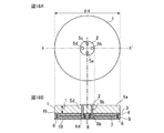
- the interface circuit 7 can be realized by a microstrip line or a coplanar line. However, this is only an example, and the interface circuit 7 may be realized by a triplate line by providing the third dielectric 9 and the ground conductor 10 as shown in FIG.
- FIG. 18A is a plan view showing another antenna device according to the first embodiment
- FIG. 18B is a cross-sectional view showing a XX ′ cross-section in FIG. 18A.
- the third dielectric 9 is a dielectric having a circular planar shape.
- the third dielectric 9 is provided at a position where the second dielectric 4 and the third dielectric 9 sandwich the interface circuit 7.
- the ground conductor 10 is provided on a plane opposite to the plane in contact with the interface circuit 7 among the two planes of the third dielectric 9.
- the plane shape of the ground conductor 10 is circular.
- the other end of the ground via 8 is connected to the ground conductor 10.
- the interface circuit 7 is sandwiched between the second dielectric 4 and the third dielectric 9. Therefore, even when the antenna device 22 shown in FIG. 18 is installed on a metal structure (not shown), a short circuit between the interface circuit 7 and the metal structure can be prevented. Therefore, it is possible to prevent the antenna performance from deteriorating due to the short circuit between the interface circuit 7 and the metal structure.
- the antenna device 22 is configured such that the transmission / reception unit 21 can switch the radiated polarization by switching between Port (1) and Port (3) as the output destination of the power of the communication signal. 7 is provided.
- the interface circuit 7 having one input and four outputs, that is, the first 180-degree hybrid 11, the first 90-degree hybrid 13, and the second 90-degree hybrid
- the antenna device 22 including the hybrid 14 may be used.
- FIG. 20A is a plan view showing the antenna device according to the second embodiment
- FIG. 20B is a cross-sectional view showing a XX ′ cross section in FIG. 20A. 20, the same reference numerals as those in FIG. 1 denote the same or corresponding parts, and a description thereof will not be repeated.
- the non-excitation ring 51 is provided on the first plane 1 a so as to surround the excitation element 2 concentrically with the excitation element 2, and is electromagnetically coupled to the excitation element 2.
- the non-excitation ring 51 has a distance ⁇ from the end of the excitation element 2 to the center diameter of the non-excitation ring 51 of 0.20 ⁇ 0 to 0. It is provided at a position in the range of .30 ⁇ 0.
- FIG. 21 is an explanatory diagram illustrating a simulation result of the lowest operation gain of the antenna device when the beam width of the electromagnetic wave is 140 degrees.
- the minimum operation gain is calculated using the distance ⁇ and the line width W of the non-exciting ring 51 as parameters.
- the thickness t of the first dielectric 1 is 0.25 ⁇ g
- the diameter ⁇ d of the first plane is 2.7 ⁇ g.
- the horizontal axis, the line width W of the parasitic rings 51 are divided by the wavelength lambda] g
- the vertical axis is a value obtained by dividing the distance ⁇ at the wavelength lambda 0.
- the distance ⁇ from the end of the excitation element 2 to the center diameter of the non-excitation ring 51 and the line width W of the non-excitation ring 51 have an optimal value for increasing the operation gain, as shown in FIG. , the distance ⁇ is operating gain is maximized when 0.25 [lambda 0. Why the actual gain is maximized when the distance ⁇ is 0.25 [lambda 0 is as follows. When the distance ⁇ is 0.25 [lambda 0, the phase of the current flowing through the excitation element 2 and the current flowing through the parasitic ring 51 phases in phase.
- the electromagnetic coupling between the excitation element 2 and the non-excitation ring 51 is strengthened, so that the gain in the zenith direction is reduced and the low elevation angle direction is reduced. Gain increases.
- the electromagnetic coupling between the excitation element 2 and the non-excitation ring 51 is weak, so that the effect of the non-excitation ring 51 cannot be sufficiently obtained.
- FIG. 22 shows the radiation of the electromagnetic wave from the excitation element 2, the radiation of the electromagnetic wave from the first power supply pin 5a, the second power supply pin 5b, the third power supply pin 5c, and the fourth power supply pin 5d.
- FIG. 4 is an explanatory diagram showing radiation of an electromagnetic wave from a ring 51.
- radiation from the non-excitation ring 51 is added as electromagnetic wave radiation, and the antenna device 22 has a high gain in a wide elevation angle range. Act as an antenna.
- the radiation of the electromagnetic wave from the non-excitation ring 51 is the radiation of the electromagnetic wave in the TM21 mode.
- Figure 23 is a first thickness t of the dielectric 1 0.25Ramudag, diameter .phi.d 2.7Ramudag, distance ⁇ is 0.25 [lambda 0, when the line width W of the parasitic rings 51 is 0.175 ⁇ g
- FIG. 9 is an explanatory diagram showing a simulation result of a radiation pattern.
- the simulation result shown in FIG. 23 shows that a high gain of 0 [dBi] or more is obtained when the zenith angle is in the range of ⁇ 90 [deg] ⁇ ⁇ +90 [deg], which is smaller than the simulation result shown in FIG. ,
- the gain in the low elevation direction is high. That is, the simulation result shown in FIG.
- the simulation result shown in FIG. 23 has a higher gain in the low elevation angle direction than the simulation result shown in FIG.
- the above-described second embodiment includes an antenna device provided with a non-exciting ring 51 provided concentrically with the exciting element 2 on the first plane 1 a so as to surround the exciting element 2 and electromagnetically coupled with the exciting element 2.
- No. 22 was constructed. Therefore, similarly to the antenna device 22 of the first embodiment, the antenna device 22 can realize wireless communication with both the high-elevation-angle communication satellite and the low-elevation-angle communication satellite. Rather, the coverage area can be expanded.
- FIG. 24A is a plan view showing the antenna device according to the third embodiment
- FIG. 24B is a cross-sectional view showing a cross section XX ′ in FIG. 24A.
- a ring-shaped dielectric (hereinafter referred to as “ring-shaped dielectric”) 61 is provided on the first plane 1 a so as to surround the excitation element 2 concentrically with the excitation element 2.
- the thickness of the ring-shaped dielectric 61 is t ′.
- the distance ⁇ from the end of the excitation element 2 to the inner diameter of the ring dielectric 61 is 0.50 ⁇ 0 or more. Is provided at the position.
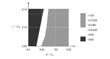
- FIG. 25 is an explanatory diagram illustrating a simulation result of the lowest operation gain of the antenna device when the beam width of the electromagnetic wave is 140 degrees.
- the minimum operation gain is calculated using the distance ⁇ and the thickness t ′ of the ring-shaped dielectric 61 as parameters.
- the thickness t of the first dielectric 1 is 0.25 ⁇ g and the diameter ⁇ d of the first plane is 2.7 ⁇ g.
- the relative permittivity of the ring-shaped dielectric 61 is 3.62, and the dielectric loss tangent of the ring-shaped dielectric 61 is 0.005.
- the relative permittivity of the ring-shaped dielectric 61 may be the same as or different from the relative permittivity of the first dielectric 1.
- the horizontal axis is a value obtained by dividing the distance ⁇ by the wavelength ⁇ 0
- the vertical axis is a value obtained by dividing the thickness t ′ of the ring-shaped dielectric 61 by the wavelength ⁇ g.
- the distance ⁇ from the end of the excitation element 2 to the inner diameter of the ring-shaped dielectric 61 and the thickness t ′ of the ring-shaped dielectric 61 have an optimum value for increasing the operation gain. as shown, the distance ⁇ is the 0.50Ramuda 0 or more, and is 0.75 [dBi] over a high gain.
- the thickness of the dielectric at the position where the ring-shaped dielectric 61 is provided becomes t + t ', and at the position where the ring-shaped dielectric 61 is not provided. It becomes thicker than the thickness t of the dielectric. Therefore, the thickness of the dielectric becomes discontinuous.
- the magnetic energy concentrates on the position where the ring-shaped dielectric 61 is provided in the range where the thickness is large. That is, magnetic energy concentrates between the ring-shaped dielectric 61 and the ground conductor 3.
- the distance from the end of the excitation element 2 to the inner diameter of the ring shaped dielectric 61 delta ring-shaped dielectric 61 is provided at a position of 0.50 ⁇ 0, are accumulated between the excitation element 2 and the ground conductor 3
- the phase of the magnetic current is the same as the phase of the magnetic current accumulated between the ring-shaped dielectric 61 and the ground conductor 3. Since the phases of the magnetic currents are in phase, the radiation of the electromagnetic wave from the excitation element 2 and the first power supply pin 5a, the second power supply pin 5b, the third power supply pin 5c, and the fourth power supply pin 5d The radiation of the electromagnetic waves from the antenna device 22 is superimposed, so that the antenna device 22 is widened.
- the antenna device 22 is configured to include the ring-shaped dielectric 61 provided on the first plane 1a so as to surround the excitation element 2 concentrically with the excitation element 2. Therefore, similarly to the antenna device 22 of the first embodiment, the antenna device 22 can realize wireless communication with both the high-elevation-angle communication satellite and the low-elevation-angle communication satellite. Rather, the coverage area can be expanded.
- any combination of the embodiments, a modification of an arbitrary component of each embodiment, or an omission of an arbitrary component in each embodiment is possible within the scope of the invention. .
- the present invention is suitable for an antenna device in which an excitation element is provided on a plane of a dielectric. Further, the present invention is suitable for a communication device including an antenna device.
Landscapes
- Waveguide Aerials (AREA)
Abstract
第1の誘電体(1)の第1の平面(1a)及び第2の平面(1b)におけるそれぞれの直径φdと、第1の誘電体(1)の厚さtとが、電磁波のビーム幅及び電磁波の帯域幅のそれぞれに基づいて決定されているように、アンテナ装置(22)を構成した。
Description
この発明は、誘電体の平面に励振素子が設けられているアンテナ装置と、アンテナ装置を備える通信装置とに関するものである。
衛星通信用のアンテナ装置は、指向方向が、天頂方向などの高仰角方向であれば、高仰角方向に存在している衛星に実装されている通信装置(以下、「高仰角通信衛星」と称する)との無線通信を実現することができる。
また、衛星通信用のアンテナ装置は、指向方向が、高仰角方向の仰角よりも仰角が低い方向である低仰角方向であれば、低仰角方向に存在している衛星に実装されている通信装置(以下、「低仰角通信衛星」と称する)との無線通信を実現することができる。
また、衛星通信用のアンテナ装置は、指向方向が、高仰角方向の仰角よりも仰角が低い方向である低仰角方向であれば、低仰角方向に存在している衛星に実装されている通信装置(以下、「低仰角通信衛星」と称する)との無線通信を実現することができる。
高仰角方向への指向性が強いアンテナ方式のアンテナ装置として、パッチアンテナを備えるアンテナ装置が知られている。
しかし、パッチアンテナは、低仰角になるほど、指向性が弱くなるため、パッチアンテナを備えるアンテナ装置は、低仰角通信衛星との無線通信を実現できないことがある。
パッチアンテナを小型化することで、パッチアンテナの放射パターンとして、広覆域な放射パターンを得ることは可能である。広覆域な放射パターンが得られれば、アンテナ装置は、高仰角通信衛星との無線通信を実現できるとともに、低仰角通信衛星との無線通信を実現できる。
ただし、パッチアンテナを小型化することで、アンテナ装置が送受信できる電磁波の帯域幅が狭くなるため、使用可能な電磁波の周波数範囲が制限される。
しかし、パッチアンテナは、低仰角になるほど、指向性が弱くなるため、パッチアンテナを備えるアンテナ装置は、低仰角通信衛星との無線通信を実現できないことがある。
パッチアンテナを小型化することで、パッチアンテナの放射パターンとして、広覆域な放射パターンを得ることは可能である。広覆域な放射パターンが得られれば、アンテナ装置は、高仰角通信衛星との無線通信を実現できるとともに、低仰角通信衛星との無線通信を実現できる。
ただし、パッチアンテナを小型化することで、アンテナ装置が送受信できる電磁波の帯域幅が狭くなるため、使用可能な電磁波の周波数範囲が制限される。
以下の特許文献1には、放射電極を取り囲むようにリング状の無給電電極が配置されているパッチアンテナが開示されている。
パッチアンテナは、無給電電極を備えることで、天頂方向への指向性が低下するが、低仰角方向への指向性が向上する。
パッチアンテナは、無給電電極を備えることで、天頂方向への指向性が低下するが、低仰角方向への指向性が向上する。
特許文献1に開示されているパッチアンテナは、使用可能な電磁波の狭帯域化を招くことなく、低仰角方向への指向性を強めることができる。
しかし、天頂方向への指向性は、低下してしまうため、天頂方向に存在している衛星に実装されている通信装置との無線通信を実現できなくなってしまうことがあるという課題があった。
しかし、天頂方向への指向性は、低下してしまうため、天頂方向に存在している衛星に実装されている通信装置との無線通信を実現できなくなってしまうことがあるという課題があった。
この発明は上記のような課題を解決するためになされたもので、使用可能な電磁波の狭帯域化を招くことなく、高仰角通信衛星及び低仰角通信衛星の双方との無線通信を実現することができるアンテナ装置及び通信装置を得ることを目的とする。
この発明に係るアンテナ装置は、第1の平面と、第1の平面と反対側の面である第2の平面とを有し、第1及び第2の平面の形状が円形である第1の誘電体と、第1の平面に設けられ、電磁波を放射又は受信する励振素子と、第2の平面に設けられている地導体と、地導体における2つの平面のうち、第2の平面と接している側の平面と反対側の平面に設けられている第2の誘電体と、一端が励振素子と接続され、他端が給電点であり、地導体と電気的に非接触の状態で、第1の誘電体及び第2の誘電体のそれぞれを貫通している給電ピンとを備え、第1及び第2の平面の直径、及び、第1の誘電体の厚さのそれぞれが、電磁波のビーム幅及び電磁波の帯域幅のそれぞれに基づいて決定されているものである。
この発明によれば、第1及び第2の平面の直径、及び、第1の誘電体の厚さのそれぞれが、電磁波のビーム幅及び電磁波の帯域幅のそれぞれに基づいて決定されているように、アンテナ装置を構成した。したがって、この発明に係るアンテナ装置は、使用可能な電磁波の狭帯域化を招くことなく、高仰角通信衛星及び低仰角通信衛星の双方との無線通信を実現することができる。
以下、この発明をより詳細に説明するために、この発明を実施するための形態について、添付の図面に従って説明する。
実施の形態1.
図1Aは、実施の形態1によるアンテナ装置を示す平面図であり、図1Bは、図1AにおけるX-X’断面を示す断面図である。
図1において、第1の誘電体1は、第1の平面1aと、第1の平面1aと反対側の面である第2の平面1bとを有している。
第1の平面1a及び第2の平面1bにおけるそれぞれの形状は、直径φdの円形であり、直径φdは、励振素子2から放射又は励振素子2により受信される電磁波のビーム幅及び当該電磁波の帯域幅のそれぞれに基づいて決定されている。
第1の誘電体1の厚さは、tである。第1の誘電体1の厚さtについても、直径φdと同様に、励振素子2から放射又は励振素子2により受信される電磁波のビーム幅及び当該電磁波の帯域幅のそれぞれに基づいて決定されている。
図1Aは、実施の形態1によるアンテナ装置を示す平面図であり、図1Bは、図1AにおけるX-X’断面を示す断面図である。
図1において、第1の誘電体1は、第1の平面1aと、第1の平面1aと反対側の面である第2の平面1bとを有している。
第1の平面1a及び第2の平面1bにおけるそれぞれの形状は、直径φdの円形であり、直径φdは、励振素子2から放射又は励振素子2により受信される電磁波のビーム幅及び当該電磁波の帯域幅のそれぞれに基づいて決定されている。
第1の誘電体1の厚さは、tである。第1の誘電体1の厚さtについても、直径φdと同様に、励振素子2から放射又は励振素子2により受信される電磁波のビーム幅及び当該電磁波の帯域幅のそれぞれに基づいて決定されている。
励振素子2は、第1の誘電体1における第1の平面1aに設けられており、電磁波を放射又は受信する。
励振素子2の平面形状は、円形である。励振素子2の直径は、励振素子2の共振周波数に対応しており、例えば、共振周波数で2分の1波長の長さがよい。ただし、これは一例に過ぎず、励振素子2の直径は、共振周波数で2分の1波長の長さよりも長くてもよいし、短くてもよい。
励振素子2の平面形状は、円形である。励振素子2の直径は、励振素子2の共振周波数に対応しており、例えば、共振周波数で2分の1波長の長さがよい。ただし、これは一例に過ぎず、励振素子2の直径は、共振周波数で2分の1波長の長さよりも長くてもよいし、短くてもよい。
地導体3は、第1の誘電体1における第2の平面1bに設けられている。
ただし、地導体3は、第1の給電ピン5a、第2の給電ピン5b、第3の給電ピン5c及び第4の給電ピン5dと接触しないように、第2の平面のうち、第1の給電ピン5a、第2の給電ピン5b、第3の給電ピン5c及び第4の給電ピン5dが第1の誘電体1を貫通している部分の周辺には設けられていない。
地導体3の平面形状は、円形である。
第2の誘電体4は、地導体3における2つの平面のうち、第2の平面1bと接している側の平面と反対側の平面に設けられている。
第2の誘電体4の平面形状は、円形である。
ただし、地導体3は、第1の給電ピン5a、第2の給電ピン5b、第3の給電ピン5c及び第4の給電ピン5dと接触しないように、第2の平面のうち、第1の給電ピン5a、第2の給電ピン5b、第3の給電ピン5c及び第4の給電ピン5dが第1の誘電体1を貫通している部分の周辺には設けられていない。
地導体3の平面形状は、円形である。
第2の誘電体4は、地導体3における2つの平面のうち、第2の平面1bと接している側の平面と反対側の平面に設けられている。
第2の誘電体4の平面形状は、円形である。
図1に示すアンテナ装置は、複数の給電ピンとして、第1の給電ピン5a、第2の給電ピン5b、第3の給電ピン5c及び第4の給電ピン5dを備えている。
第1の給電ピン5a、第2の給電ピン5b、第3の給電ピン5c及び第4の給電ピン5dにおけるそれぞれの一端は、励振素子2と接続されている。
第1の給電ピン5a、第2の給電ピン5b、第3の給電ピン5c及び第4の給電ピン5dにおけるそれぞれの一端は、回転対称に配置されている。
第1の給電ピン5aの他端は、給電点6aであり、第2の給電ピン5bの他端は、給電点6bである。また、第3の給電ピン5cの他端は、給電点6cであり、第4の給電ピン5dの他端は、給電点6dである。図1は、給電点6a及び給電点6cの記載を省略している。
第1の給電ピン5a、第2の給電ピン5b、第3の給電ピン5c及び第4の給電ピン5dは、地導体3と電気的に非接触の状態で、第1の誘電体1及び第2の誘電体4のそれぞれを貫通している。
なお、給電点6a,6b,6c,6dは、アンテナ装置の物理的な構成要素として形成されているものではなく、インタフェース回路7から電力が供給される給電ピンの位置を示すものである。
第1の給電ピン5a、第2の給電ピン5b、第3の給電ピン5c及び第4の給電ピン5dにおけるそれぞれの一端は、励振素子2と接続されている。
第1の給電ピン5a、第2の給電ピン5b、第3の給電ピン5c及び第4の給電ピン5dにおけるそれぞれの一端は、回転対称に配置されている。
第1の給電ピン5aの他端は、給電点6aであり、第2の給電ピン5bの他端は、給電点6bである。また、第3の給電ピン5cの他端は、給電点6cであり、第4の給電ピン5dの他端は、給電点6dである。図1は、給電点6a及び給電点6cの記載を省略している。
第1の給電ピン5a、第2の給電ピン5b、第3の給電ピン5c及び第4の給電ピン5dは、地導体3と電気的に非接触の状態で、第1の誘電体1及び第2の誘電体4のそれぞれを貫通している。
なお、給電点6a,6b,6c,6dは、アンテナ装置の物理的な構成要素として形成されているものではなく、インタフェース回路7から電力が供給される給電ピンの位置を示すものである。
インタフェース回路7は、第2の誘電体4における2つの平面のうち、地導体3と接している側の平面と反対側の平面に設けられている。
インタフェース回路7は、第1の給電ピン5a、第2の給電ピン5b、第3の給電ピン5c及び第4の給電ピン5dにおけるそれぞれの他端と接続されている。
インタフェース回路7は、第1の給電ピン5a、第2の給電ピン5b、第3の給電ピン5c及び第4の給電ピン5dにおけるそれぞれの他端に、振幅が同じで、位相が異なる電力を与える。
グランドビア8は、一端が地導体3と接続され、他端がインタフェース回路7と接続されており、第2の誘電体4を貫通している。
インタフェース回路7は、第1の給電ピン5a、第2の給電ピン5b、第3の給電ピン5c及び第4の給電ピン5dにおけるそれぞれの他端と接続されている。
インタフェース回路7は、第1の給電ピン5a、第2の給電ピン5b、第3の給電ピン5c及び第4の給電ピン5dにおけるそれぞれの他端に、振幅が同じで、位相が異なる電力を与える。
グランドビア8は、一端が地導体3と接続され、他端がインタフェース回路7と接続されており、第2の誘電体4を貫通している。
第1の平面1a及び第2の平面1bにおけるそれぞれの形状が円形であり、励振素子2、地導体3及び第2の誘電体4におけるそれぞれの平面形状が円形である理由は、対称性の良い構造とすることで、異なる方位の間での利得偏差を低減するためである。
図1に示すアンテナ装置は、4点給電の円偏波アンテナを示しており、第1の給電ピン5a、第2の給電ピン5b、第3の給電ピン5c及び第4の給電ピン5dの一端が、回転対称な位置に配置されている。第1の給電ピン5a、第2の給電ピン5b、第3の給電ピン5c及び第4の給電ピン5dの一端が、回転対称な位置に配置されているため、異なる方位の間での利得偏差が低減されている。
図1に示すアンテナ装置は、4点給電の円偏波アンテナを示している。しかし、これは一例に過ぎず、例えば、1点給電の円偏波アンテナであってもよいし、2点給電の円偏波アンテナであってもよい。
ただし、給電ピンの一端が回転対称な位置ではなく、非対称的な位置に配置されるアンテナ装置では、図1に示すアンテナ装置よりも、異なる方位の間での利得偏差が増加する。
図1に示すアンテナ装置は、4点給電の円偏波アンテナを示しており、第1の給電ピン5a、第2の給電ピン5b、第3の給電ピン5c及び第4の給電ピン5dの一端が、回転対称な位置に配置されている。第1の給電ピン5a、第2の給電ピン5b、第3の給電ピン5c及び第4の給電ピン5dの一端が、回転対称な位置に配置されているため、異なる方位の間での利得偏差が低減されている。
図1に示すアンテナ装置は、4点給電の円偏波アンテナを示している。しかし、これは一例に過ぎず、例えば、1点給電の円偏波アンテナであってもよいし、2点給電の円偏波アンテナであってもよい。
ただし、給電ピンの一端が回転対称な位置ではなく、非対称的な位置に配置されるアンテナ装置では、図1に示すアンテナ装置よりも、異なる方位の間での利得偏差が増加する。
図2は、実施の形態1によるアンテナ装置のインタフェース回路7を示す構成図であり、図3は、図2に示すインタフェース回路7のレイアウトを示す説明図である。
図3に示すレイアウトは、励振素子2からインタフェース回路7の方向を見たときのレイアウトを示している。
図2及び図3において、Port(1)は、後述する送受信部21と接続されている。
Port(1)は、図1に示すアンテナ装置を、天頂方向にRHCP(右旋円偏波)の交差偏波を放射し、地面方向にLHCP(左旋円偏波)の交差偏波を放射する円偏波アンテナとして用いる場合に、送受信部21から電力が与えられるポートである。ここでは、天頂方向は、仰角が約90度の方向であり、地面方向は、仰角が約0度の方向であるとする。
送受信部21からPort(1)に電力が与えられる場合、Port(2)、Port(3)及びPort(4)には、送受信部21から電力が与えられない。
Port(2)とPort(4)は、グランドビア8の他端と接続されているポートである。
図3に示すレイアウトは、励振素子2からインタフェース回路7の方向を見たときのレイアウトを示している。
図2及び図3において、Port(1)は、後述する送受信部21と接続されている。
Port(1)は、図1に示すアンテナ装置を、天頂方向にRHCP(右旋円偏波)の交差偏波を放射し、地面方向にLHCP(左旋円偏波)の交差偏波を放射する円偏波アンテナとして用いる場合に、送受信部21から電力が与えられるポートである。ここでは、天頂方向は、仰角が約90度の方向であり、地面方向は、仰角が約0度の方向であるとする。
送受信部21からPort(1)に電力が与えられる場合、Port(2)、Port(3)及びPort(4)には、送受信部21から電力が与えられない。
Port(2)とPort(4)は、グランドビア8の他端と接続されているポートである。
Port(3)は、送受信部21と接続されているポートである。
Port(3)は、図1に示すアンテナ装置を、天頂方向にLHCPの交差偏波を放射し、地面方向にRHCPの交差偏波を放射する円偏波アンテナとして用いる場合に、送受信部21から電力が与えられるポートである。
送受信部21からPort(3)に電力が与えられる場合、Port(1)、Port(2)及びPort(4)には、送受信部21から電力が与えられない。
Port(2)とPort(4)は、グランドビア8の他端と接続されているポートである。
Port(3)は、図1に示すアンテナ装置を、天頂方向にLHCPの交差偏波を放射し、地面方向にRHCPの交差偏波を放射する円偏波アンテナとして用いる場合に、送受信部21から電力が与えられるポートである。
送受信部21からPort(3)に電力が与えられる場合、Port(1)、Port(2)及びPort(4)には、送受信部21から電力が与えられない。
Port(2)とPort(4)は、グランドビア8の他端と接続されているポートである。
Port(5)は、第1の給電ピン5aの他端である給電点6aと接続されているポートである。
Port(6)は、第2の給電ピン5bの他端である給電点6bと接続されている。
Port(7)は、第3の給電ピン5cの他端である給電点6cと接続されている。
Port(8)は、第4の給電ピン5dの他端である給電点6dと接続されている。
Port(6)は、第2の給電ピン5bの他端である給電点6bと接続されている。
Port(7)は、第3の給電ピン5cの他端である給電点6cと接続されている。
Port(8)は、第4の給電ピン5dの他端である給電点6dと接続されている。
第1の180度ハイブリッド11は、第1の端子11a、第2の端子11b、第3の端子11c及び第4の端子11dを有している。
第1の端子11aは、Port(1)と接続され、第2の端子11bは、Port(2)と接続されている。
第3の端子11cは、第1の90度ハイブリッド13の第1の端子13aと接続され、第4の端子11dは、第2の90度ハイブリッド14の第1の端子14aと接続されている。
第1の180度ハイブリッド11は、送受信部21からPort(1)を介して第1の端子11aに電力が与えられると、第3の端子11cから位相が-90度の電力を出力するとともに、第4の端子11dから位相が-270度の電力を出力する。
第3の端子11cから出力された位相が-90度の電力は、第1の90度ハイブリッド13の第1の端子13aに入力される。
第4の端子11dから出力された位相が-270度の電力は、第2の90度ハイブリッド14の第1の端子14aに入力される。
第1の端子11aは、Port(1)と接続され、第2の端子11bは、Port(2)と接続されている。
第3の端子11cは、第1の90度ハイブリッド13の第1の端子13aと接続され、第4の端子11dは、第2の90度ハイブリッド14の第1の端子14aと接続されている。
第1の180度ハイブリッド11は、送受信部21からPort(1)を介して第1の端子11aに電力が与えられると、第3の端子11cから位相が-90度の電力を出力するとともに、第4の端子11dから位相が-270度の電力を出力する。
第3の端子11cから出力された位相が-90度の電力は、第1の90度ハイブリッド13の第1の端子13aに入力される。
第4の端子11dから出力された位相が-270度の電力は、第2の90度ハイブリッド14の第1の端子14aに入力される。
第2の180度ハイブリッド12は、第1の端子12a、第2の端子12b、第3の端子12c及び第4の端子12dを有している。
第1の端子12aは、Port(3)と接続され、第2の端子12bは、Port(4)と接続されている。
第3の端子12cは、第1の90度ハイブリッド13の第2の端子13bと接続され、第4の端子12dは、第2の90度ハイブリッド14の第2の端子14bと接続されている。
第2の180度ハイブリッド12は、送受信部21からPort(3)を介して第1の端子12aに電力が与えられると、第3の端子12cから位相が-90度の電力を出力するとともに、第4の端子12dから位相が-270度の電力を出力する。
第3の端子12cから出力された位相が-90度の電力は、第1の90度ハイブリッド13の第2の端子13bに入力される。
第4の端子12dから出力された位相が-270度の電力は、第2の90度ハイブリッド14の第2の端子14bに入力される。
第1の端子12aは、Port(3)と接続され、第2の端子12bは、Port(4)と接続されている。
第3の端子12cは、第1の90度ハイブリッド13の第2の端子13bと接続され、第4の端子12dは、第2の90度ハイブリッド14の第2の端子14bと接続されている。
第2の180度ハイブリッド12は、送受信部21からPort(3)を介して第1の端子12aに電力が与えられると、第3の端子12cから位相が-90度の電力を出力するとともに、第4の端子12dから位相が-270度の電力を出力する。
第3の端子12cから出力された位相が-90度の電力は、第1の90度ハイブリッド13の第2の端子13bに入力される。
第4の端子12dから出力された位相が-270度の電力は、第2の90度ハイブリッド14の第2の端子14bに入力される。
第1の90度ハイブリッド13は、第1の端子13a、第2の端子13b、第3の端子13c及び第4の端子13dを有している。
第1の端子13aは、第1の180度ハイブリッド11の第3の端子11cと接続され、第2の端子13bは、第2の180度ハイブリッド12の第3の端子12cと接続されている。
第3の端子13cは、Port(5)と接続され、第4の端子13dは、Port(6)と接続されている。
第1の90度ハイブリッド13は、第1の180度ハイブリッド11の第3の端子11cから第1の端子13aに位相が-90度の電力が与えられると、第3の端子13cから位相が-180度の電力を出力するとともに、第4の端子13dから位相が-270度の電力を出力する。
第3の端子13cから出力された位相が-180度の電力は、Port(5)を介して給電点6aに入力される。
第4の端子12dから出力された位相が-270度の電力は、Port(6)を介して給電点6bに入力される。
第1の90度ハイブリッド13は、第2の180度ハイブリッド12の第3の端子12cから第2の端子13bに位相が-90度の電力が与えられると、第3の端子13cから位相が-270度の電力を出力するとともに、第4の端子13dから位相が-180度の電力を出力する。
第3の端子13cから出力された位相が-270度の電力は、Port(5)を介して給電点6aに入力される。
第4の端子13dから出力された位相が-180度の電力は、Port(6)を介して給電点6bに入力される。
第1の端子13aは、第1の180度ハイブリッド11の第3の端子11cと接続され、第2の端子13bは、第2の180度ハイブリッド12の第3の端子12cと接続されている。
第3の端子13cは、Port(5)と接続され、第4の端子13dは、Port(6)と接続されている。
第1の90度ハイブリッド13は、第1の180度ハイブリッド11の第3の端子11cから第1の端子13aに位相が-90度の電力が与えられると、第3の端子13cから位相が-180度の電力を出力するとともに、第4の端子13dから位相が-270度の電力を出力する。
第3の端子13cから出力された位相が-180度の電力は、Port(5)を介して給電点6aに入力される。
第4の端子12dから出力された位相が-270度の電力は、Port(6)を介して給電点6bに入力される。
第1の90度ハイブリッド13は、第2の180度ハイブリッド12の第3の端子12cから第2の端子13bに位相が-90度の電力が与えられると、第3の端子13cから位相が-270度の電力を出力するとともに、第4の端子13dから位相が-180度の電力を出力する。
第3の端子13cから出力された位相が-270度の電力は、Port(5)を介して給電点6aに入力される。
第4の端子13dから出力された位相が-180度の電力は、Port(6)を介して給電点6bに入力される。
第2の90度ハイブリッド14は、第1の端子14a、第2の端子14b、第3の端子14c及び第4の端子14dを有している。
第1の端子14aは、第1の180度ハイブリッド11の第4の端子11dと接続され、第2の端子14bは、第2の180度ハイブリッド12の第4の端子12dと接続されている。
第3の端子14cは、Port(7)と接続され、第4の端子14dは、Port(8)と接続されている。
第2の90度ハイブリッド14は、第1の180度ハイブリッド11の第4の端子11dから第1の端子14aに位相が-270度の電力が与えられると、第3の端子14cから位相が0度の電力を出力するとともに、第4の端子14dから位相が-90度の電力を出力する。
第3の端子14cから出力された位相が0度の電力は、Port(7)を介して給電点6cに入力される。
第4の端子14dから出力された位相が-90度の電力は、Port(8)を介して給電点6dに入力される。
第2の90度ハイブリッド14は、第2の180度ハイブリッド12の第4の端子12dから第2の端子14bに位相が-270度の電力が与えられると、第3の端子13cから位相が-90度の電力を出力するとともに、第4の端子14dから位相が0度の電力を出力する。
第3の端子14cから出力された位相が-90度の電力は、Port(7)を介して給電点6cに入力される。
第4の端子14dから出力された位相が0度の電力は、Port(8)を介して給電点6dに入力される。
第1の端子14aは、第1の180度ハイブリッド11の第4の端子11dと接続され、第2の端子14bは、第2の180度ハイブリッド12の第4の端子12dと接続されている。
第3の端子14cは、Port(7)と接続され、第4の端子14dは、Port(8)と接続されている。
第2の90度ハイブリッド14は、第1の180度ハイブリッド11の第4の端子11dから第1の端子14aに位相が-270度の電力が与えられると、第3の端子14cから位相が0度の電力を出力するとともに、第4の端子14dから位相が-90度の電力を出力する。
第3の端子14cから出力された位相が0度の電力は、Port(7)を介して給電点6cに入力される。
第4の端子14dから出力された位相が-90度の電力は、Port(8)を介して給電点6dに入力される。
第2の90度ハイブリッド14は、第2の180度ハイブリッド12の第4の端子12dから第2の端子14bに位相が-270度の電力が与えられると、第3の端子13cから位相が-90度の電力を出力するとともに、第4の端子14dから位相が0度の電力を出力する。
第3の端子14cから出力された位相が-90度の電力は、Port(7)を介して給電点6cに入力される。
第4の端子14dから出力された位相が0度の電力は、Port(8)を介して給電点6dに入力される。
図3に示すレイアウトは、無駄な電力の損失を減らすために、第1の180度ハイブリッド11、第2の180度ハイブリッド12、第1の90度ハイブリッド13及び第2の90度ハイブリッド14の間の伝送線路を短くしているレイアウトの一例である。
図3に示すレイアウトでは、伝送線路を短くするために、第2の180度ハイブリッド12と第1の90度ハイブリッド13の間を結ぶ伝送線路が、第1の90度ハイブリッド13と第2の90度ハイブリッド14との間を通されている。
なお、インタフェース回路7は、エッチングでパターン形成されているものであってもよいし、チップ部品で構成されているものであってもよい。
図3に示すレイアウトでは、伝送線路を短くするために、第2の180度ハイブリッド12と第1の90度ハイブリッド13の間を結ぶ伝送線路が、第1の90度ハイブリッド13と第2の90度ハイブリッド14との間を通されている。
なお、インタフェース回路7は、エッチングでパターン形成されているものであってもよいし、チップ部品で構成されているものであってもよい。
図4は、実施の形態1による通信装置を示す構成図である。
図4において、送受信部21は、Port(1)及びPort(3)を介して、アンテナ装置22と接続されている。
送受信部21は、通信信号を送信する場合において、天頂方向にRHCPの交差偏波を放射し、地面方向にLHCPの交差偏波を放射する場合、通信信号の電力をPort(1)に与える。
送受信部21は、通信信号を送信する場合において、天頂方向にLHCPの交差偏波を放射し、地面方向にRHCPの交差偏波を放射する場合、通信信号の電力をPort(3)に与える。
送受信部21は、通信信号を受信する場合、Port(1)又はPort(3)から、通信信号の電力を取得する。
アンテナ装置22は、図1に示すアンテナ装置であり、Port(1)及びPort(3)を介して、送受信部21と接続されている。
図4において、送受信部21は、Port(1)及びPort(3)を介して、アンテナ装置22と接続されている。
送受信部21は、通信信号を送信する場合において、天頂方向にRHCPの交差偏波を放射し、地面方向にLHCPの交差偏波を放射する場合、通信信号の電力をPort(1)に与える。
送受信部21は、通信信号を送信する場合において、天頂方向にLHCPの交差偏波を放射し、地面方向にRHCPの交差偏波を放射する場合、通信信号の電力をPort(3)に与える。
送受信部21は、通信信号を受信する場合、Port(1)又はPort(3)から、通信信号の電力を取得する。
アンテナ装置22は、図1に示すアンテナ装置であり、Port(1)及びPort(3)を介して、送受信部21と接続されている。
次に、図4に示す通信装置の動作について説明する。
図1に示すアンテナ装置を、交差偏波を放射する円偏波アンテナとして用いる場合について説明する。
送受信部21は、天頂方向にRHCPの交差偏波を放射し、地面方向にLHCPの交差偏波を放射する場合、通信信号の電力を、Port(1)を介して、第1の180度ハイブリッド11の第1の端子11aに出力する。
送受信部21から通信信号の電力が、Port(1)を介して、第1の180度ハイブリッド11の第1の端子11aに出力されているとき、Port(2)、Port(3)及びPort(4)の間のアイソレーションは、確保されている。
図1に示すアンテナ装置を、交差偏波を放射する円偏波アンテナとして用いる場合について説明する。
送受信部21は、天頂方向にRHCPの交差偏波を放射し、地面方向にLHCPの交差偏波を放射する場合、通信信号の電力を、Port(1)を介して、第1の180度ハイブリッド11の第1の端子11aに出力する。
送受信部21から通信信号の電力が、Port(1)を介して、第1の180度ハイブリッド11の第1の端子11aに出力されているとき、Port(2)、Port(3)及びPort(4)の間のアイソレーションは、確保されている。
第1の180度ハイブリッド11は、第1の端子11aに通信信号の電力が与えられると、第3の端子11cから位相が-90度の電力を第1の90度ハイブリッド13の第1の端子13aに出力する。
また、第1の180度ハイブリッド11は、第4の端子11dから位相が-270度の電力を第2の90度ハイブリッド14の第1の端子14aに出力する。
天頂方向にRHCPの交差偏波を放射し、地面方向にLHCPの交差偏波を放射する場合、送受信部21からPort(3)には、通信信号の電力が与えられない。
したがって、第2の180度ハイブリッド12の第3の端子12c及び第4の端子12dのそれぞれからは、電力が出力されない。
また、第1の180度ハイブリッド11は、第4の端子11dから位相が-270度の電力を第2の90度ハイブリッド14の第1の端子14aに出力する。
天頂方向にRHCPの交差偏波を放射し、地面方向にLHCPの交差偏波を放射する場合、送受信部21からPort(3)には、通信信号の電力が与えられない。
したがって、第2の180度ハイブリッド12の第3の端子12c及び第4の端子12dのそれぞれからは、電力が出力されない。
第1の90度ハイブリッド13は、第1の180度ハイブリッド11の第3の端子11cから第1の端子13aに位相が-90度の電力が与えられると、第3の端子13cから位相が-180度の電力を、Port(5)を介して給電点6aに出力する。
また、第1の90度ハイブリッド13は、第4の端子13dから位相が-270度の電力を、Port(6)を介して給電点6bに出力する。
第2の90度ハイブリッド14は、第1の180度ハイブリッド11の第4の端子11dから第1の端子14aに位相が-270度の電力が与えられると、第3の端子14cから位相が0度の電力を、Port(7)を介して給電点6cに出力する。
また、第2の90度ハイブリッド14は、第4の端子14dから位相が-90度の電力を、Port(8)を介して給電点6dに出力する。
また、第1の90度ハイブリッド13は、第4の端子13dから位相が-270度の電力を、Port(6)を介して給電点6bに出力する。
第2の90度ハイブリッド14は、第1の180度ハイブリッド11の第4の端子11dから第1の端子14aに位相が-270度の電力が与えられると、第3の端子14cから位相が0度の電力を、Port(7)を介して給電点6cに出力する。
また、第2の90度ハイブリッド14は、第4の端子14dから位相が-90度の電力を、Port(8)を介して給電点6dに出力する。
このとき、給電点6a、給電点6b、給電点6c及び給電点6dのそれぞれに与えられた電力の振幅は、同一であり、それぞれに与えられた電力の位相は、互いに異なっている。
そして、給電点6aに与えられた位相が-180度の電力は、図1Aにおいて、一端が6時の位置に配置されている第1の給電ピン5aの一端まで伝送される。
給電点6bに与えられた位相が-270度の電力は、図1Aにおいて、一端が3時の位置に配置されている第2の給電ピン5bの一端まで伝送される。
給電点6cに与えられた位相が0度の電力は、図1Aにおいて、一端が12時の位置に配置されている第3の給電ピン5cの一端まで伝送される。
給電点6dに与えられた位相が-90度の電力は、図1Aにおいて、一端が9時の位置に配置されている第4の給電ピン5dの一端まで伝送される。
そして、給電点6aに与えられた位相が-180度の電力は、図1Aにおいて、一端が6時の位置に配置されている第1の給電ピン5aの一端まで伝送される。
給電点6bに与えられた位相が-270度の電力は、図1Aにおいて、一端が3時の位置に配置されている第2の給電ピン5bの一端まで伝送される。
給電点6cに与えられた位相が0度の電力は、図1Aにおいて、一端が12時の位置に配置されている第3の給電ピン5cの一端まで伝送される。
給電点6dに与えられた位相が-90度の電力は、図1Aにおいて、一端が9時の位置に配置されている第4の給電ピン5dの一端まで伝送される。
第1の給電ピン5a、第2の給電ピン5b、第3の給電ピン5c及び第4の給電ピン5dにおけるそれぞれの一端に、上記の電力が伝送されることで、励振素子2が励振する。
励振素子2が励振することで、励振素子2から天頂方向にRHCPの交差偏波が放射され、地面方向にLHCPの交差偏波が放射される。
励振素子2が励振することで、励振素子2から天頂方向にRHCPの交差偏波が放射され、地面方向にLHCPの交差偏波が放射される。
送受信部21は、天頂方向にLHCPの交差偏波を放射し、地面方向にRHCPの交差偏波を放射する場合、通信信号の電力を、Port(3)を介して、第2の180度ハイブリッド12の第1の端子12aに出力する。
送受信部21から通信信号の電力が、Port(3)を介して、第2の180度ハイブリッド12の第1の端子12aに出力されているとき、Port(1)、Port(3)及びPort(4)の間のアイソレーションは、確保されている。
送受信部21から通信信号の電力が、Port(3)を介して、第2の180度ハイブリッド12の第1の端子12aに出力されているとき、Port(1)、Port(3)及びPort(4)の間のアイソレーションは、確保されている。
第2の180度ハイブリッド12は、第1の端子12aに通信信号の電力が与えられると、第3の端子12cから位相が-90度の電力を第1の90度ハイブリッド13の第2の端子13bに出力する。
また、第2の180度ハイブリッド12は、第4の端子12dから位相が-270度の電力を第2の90度ハイブリッド14の第2の端子14bに出力する。
天頂方向にLHCPの交差偏波を放射し、地面方向にRHCPの交差偏波を放射する場合、送受信部21からPort(1)には、通信信号の電力が与えられない。
したがって、第1の180度ハイブリッド11の第3の端子11c及び第4の端子11dのそれぞれからは、電力が出力されない。
また、第2の180度ハイブリッド12は、第4の端子12dから位相が-270度の電力を第2の90度ハイブリッド14の第2の端子14bに出力する。
天頂方向にLHCPの交差偏波を放射し、地面方向にRHCPの交差偏波を放射する場合、送受信部21からPort(1)には、通信信号の電力が与えられない。
したがって、第1の180度ハイブリッド11の第3の端子11c及び第4の端子11dのそれぞれからは、電力が出力されない。
第1の90度ハイブリッド13は、第2の180度ハイブリッド12の第3の端子12cから第2の端子13bに位相が-90度の電力が与えられると、第3の端子13cから位相が-270度の電力を、Port(5)を介して給電点6aに出力する。
また、第1の90度ハイブリッド13は、第4の端子13dから位相が-180度の電力を、Port(6)を介して給電点6bに出力する。
第2の90度ハイブリッド14は、第2の180度ハイブリッド12の第4の端子12dから第2の端子14bに位相が-270度の電力が与えられると、第3の端子14cから位相が-90度の電力を、Port(7)を介して給電点6cに出力する。
また、第2の90度ハイブリッド14は、第4の端子14dから位相が0度の電力を、Port(8)を介して給電点6dに出力する。
また、第1の90度ハイブリッド13は、第4の端子13dから位相が-180度の電力を、Port(6)を介して給電点6bに出力する。
第2の90度ハイブリッド14は、第2の180度ハイブリッド12の第4の端子12dから第2の端子14bに位相が-270度の電力が与えられると、第3の端子14cから位相が-90度の電力を、Port(7)を介して給電点6cに出力する。
また、第2の90度ハイブリッド14は、第4の端子14dから位相が0度の電力を、Port(8)を介して給電点6dに出力する。
このとき、給電点6a、給電点6b、給電点6c及び給電点6dのそれぞれに与えられた電力の振幅は、同一であり、それぞれに与えられた電力の位相は、互いに異なっている。
そして、給電点6aに与えられた位相が-270度の電力は、図1Aにおいて、一端が6時の位置に配置されている第1の給電ピン5aの一端まで伝送される。
給電点6bに与えられた位相が-180度の電力は、図1Aにおいて、一端が3時の位置に配置されている第2の給電ピン5bの一端まで伝送される。
給電点6cに与えられた位相が-90度の電力は、図1Aにおいて、一端が12時の位置に配置されている第3の給電ピン5cの一端まで伝送される。
給電点6dに与えられた位相が0度の電力は、図1Aにおいて、一端が9時の位置に配置されている第4の給電ピン5dの一端まで伝送される。
そして、給電点6aに与えられた位相が-270度の電力は、図1Aにおいて、一端が6時の位置に配置されている第1の給電ピン5aの一端まで伝送される。
給電点6bに与えられた位相が-180度の電力は、図1Aにおいて、一端が3時の位置に配置されている第2の給電ピン5bの一端まで伝送される。
給電点6cに与えられた位相が-90度の電力は、図1Aにおいて、一端が12時の位置に配置されている第3の給電ピン5cの一端まで伝送される。
給電点6dに与えられた位相が0度の電力は、図1Aにおいて、一端が9時の位置に配置されている第4の給電ピン5dの一端まで伝送される。
第1の給電ピン5a、第2の給電ピン5b、第3の給電ピン5c及び第4の給電ピン5dにおけるそれぞれの一端に、上記の電力が伝送されることで、励振素子2が励振する。
励振素子2が励振することで、励振素子2から天頂方向にLHCPの交差偏波が放射され、地面方向にRHCPの交差偏波が放射される。
以上より、送受信部21が、通信信号の電力の出力先として、Port(1)とPort(3)を切り替えることで、放射する偏波を切り替えることができる。
ここでは、図1に示すアンテナ装置を、交差偏波を放射する円偏波アンテナとして用いる場合を説明している。
図1に示すアンテナ装置を、交差偏波を受信する円偏波アンテナとして用いる場合の動作は、交差偏波を放射する円偏波アンテナとして用いる場合の動作と比べて、電力の流れが反対であるだけの違いであるため、詳細な説明を省略する。
励振素子2が励振することで、励振素子2から天頂方向にLHCPの交差偏波が放射され、地面方向にRHCPの交差偏波が放射される。
以上より、送受信部21が、通信信号の電力の出力先として、Port(1)とPort(3)を切り替えることで、放射する偏波を切り替えることができる。
ここでは、図1に示すアンテナ装置を、交差偏波を放射する円偏波アンテナとして用いる場合を説明している。
図1に示すアンテナ装置を、交差偏波を受信する円偏波アンテナとして用いる場合の動作は、交差偏波を放射する円偏波アンテナとして用いる場合の動作と比べて、電力の流れが反対であるだけの違いであるため、詳細な説明を省略する。
次に、図1に示すアンテナ装置が、高仰角通信衛星との無線通信ができ、かつ、低仰角通信衛星との無線通信ができることについて説明する。
ここで、高仰角通信衛星は、高仰角方向に存在している衛星に実装されている通信装置であり、低仰角通信衛星は、低仰角方向に存在している衛星に実装されている通信装置である。
高仰角方向は、例えば、天頂方向であり、低仰角方向は、例えば、仰角が20度の方向である。
図1に示すアンテナ装置が、高仰角通信衛星との無線通信ができ、かつ、低仰角通信衛星との無線通信ができるようにするには、アンテナ装置の覆域が、仰角20度以上で高利得である必要がある。即ち、アンテナ装置における電磁波のビーム幅が140度である必要がある。
ここで、高仰角通信衛星は、高仰角方向に存在している衛星に実装されている通信装置であり、低仰角通信衛星は、低仰角方向に存在している衛星に実装されている通信装置である。
高仰角方向は、例えば、天頂方向であり、低仰角方向は、例えば、仰角が20度の方向である。
図1に示すアンテナ装置が、高仰角通信衛星との無線通信ができ、かつ、低仰角通信衛星との無線通信ができるようにするには、アンテナ装置の覆域が、仰角20度以上で高利得である必要がある。即ち、アンテナ装置における電磁波のビーム幅が140度である必要がある。
アンテナ装置における電磁波のビーム幅は、第1の平面1a及び第2の平面1bにおけるそれぞれの直径φdによって決定される。
また、アンテナ装置における電磁波のビーム幅は、第1の誘電体1の厚さtによって決定される。
ここで、図5は、電磁波のビーム幅が140度であるときのアンテナ装置の最低の絶対利得についてのシミュレーション結果を示す説明図である。
また、図6は、電磁波のビーム幅が140度であるときのアンテナ装置の最低の動作利得についてのシミュレーション結果を示す説明図である。
図5及び図6において、λgは、電磁波の中心周波数において、第1の誘電体1の内部における電磁波の波長である。
図5及び図6におけるシミュレーションでは、第1の誘電体1の比誘電率が3.62、第1の誘電体1の誘電正接が0.005であるとしている。
また、アンテナ装置における電磁波のビーム幅は、第1の誘電体1の厚さtによって決定される。
ここで、図5は、電磁波のビーム幅が140度であるときのアンテナ装置の最低の絶対利得についてのシミュレーション結果を示す説明図である。
また、図6は、電磁波のビーム幅が140度であるときのアンテナ装置の最低の動作利得についてのシミュレーション結果を示す説明図である。
図5及び図6において、λgは、電磁波の中心周波数において、第1の誘電体1の内部における電磁波の波長である。
図5及び図6におけるシミュレーションでは、第1の誘電体1の比誘電率が3.62、第1の誘電体1の誘電正接が0.005であるとしている。
図5に示すシミュレーション結果に着目すると、厚さtが、約0.15λg~約0.30λgの範囲であり、かつ、直径φdが約2.1λg~約3.0λgの範囲であるとき、0[dBi]以上の高利得になることが分かる。
また、図6に示すシミュレーション結果に着目すると、厚さtが、約0.20λg~約0.28λgの範囲であり、かつ、直径φdが約2.4λg~約3.0λgの範囲であるとき、0[dBi]以上の高利得になることが分かる。
したがって、厚さtが、約0.20λg~約0.28λgの範囲であり、かつ、直径φdが約2.4λg~約3.0λgの範囲であれば、絶対利得及び動作利得の双方において、0[dBi]以上の高利得になることが分かる。
また、図6に示すシミュレーション結果に着目すると、厚さtが、約0.20λg~約0.28λgの範囲であり、かつ、直径φdが約2.4λg~約3.0λgの範囲であるとき、0[dBi]以上の高利得になることが分かる。
したがって、厚さtが、約0.20λg~約0.28λgの範囲であり、かつ、直径φdが約2.4λg~約3.0λgの範囲であれば、絶対利得及び動作利得の双方において、0[dBi]以上の高利得になることが分かる。
第1の誘電体1の厚さtは、覆域に寄与するパラメータであると同時に、帯域幅に寄与するパラメータである。
したがって、第1の誘電体1の厚さtが薄い場合、広い帯域をカバーできなくなり、不整合損が増加する。例えば、厚さtが0.15λgである場合、不整合損が増加しており、動作利得が0[dBi]よりも小さくなっている。
第1の誘電体1の厚さtが増加することは、第1の給電ピン5a、第2の給電ピン5b、第3の給電ピン5c及び第4の給電ピン5dの長さが長くなることに相当する。例えば、第1の誘電体1の厚さtが約0.25λgである場合、図7に示すように、励振素子2からの電磁波の放射のほかに、第1の給電ピン5a、第2の給電ピン5b、第3の給電ピン5c及び第4の給電ピン5dからの電磁波の放射が加わる。第1の給電ピン5a、第2の給電ピン5b、第3の給電ピン5c及び第4の給電ピン5dからの電磁波の放射は、モノポールアンテナとしての電磁波の放射である。
図7は、励振素子2からの電磁波の放射と、第1の給電ピン5a、第2の給電ピン5b、第3の給電ピン5c及び第4の給電ピン5dからの電磁波の放射とを示す説明図である。
第1の給電ピン5a、第2の給電ピン5b、第3の給電ピン5c及び第4の給電ピン5dからの電磁波の放射が加わることで、低仰角方向の利得が増加する。
したがって、第1の誘電体1の厚さtが薄い場合、広い帯域をカバーできなくなり、不整合損が増加する。例えば、厚さtが0.15λgである場合、不整合損が増加しており、動作利得が0[dBi]よりも小さくなっている。
第1の誘電体1の厚さtが増加することは、第1の給電ピン5a、第2の給電ピン5b、第3の給電ピン5c及び第4の給電ピン5dの長さが長くなることに相当する。例えば、第1の誘電体1の厚さtが約0.25λgである場合、図7に示すように、励振素子2からの電磁波の放射のほかに、第1の給電ピン5a、第2の給電ピン5b、第3の給電ピン5c及び第4の給電ピン5dからの電磁波の放射が加わる。第1の給電ピン5a、第2の給電ピン5b、第3の給電ピン5c及び第4の給電ピン5dからの電磁波の放射は、モノポールアンテナとしての電磁波の放射である。
図7は、励振素子2からの電磁波の放射と、第1の給電ピン5a、第2の給電ピン5b、第3の給電ピン5c及び第4の給電ピン5dからの電磁波の放射とを示す説明図である。
第1の給電ピン5a、第2の給電ピン5b、第3の給電ピン5c及び第4の給電ピン5dからの電磁波の放射が加わることで、低仰角方向の利得が増加する。
また、直径φdが大きくなると、アンテナ装置22から放射された電磁波は、第1の誘電体1の第1の平面1a付近を表面波として伝搬されるようになるため、低仰角方向の利得が増加する。
以上より、高仰角通信衛星との無線通信ができ、かつ、低仰角通信衛星との無線通信ができる厚さt及び直径φdが存在することが分かる。
以上より、高仰角通信衛星との無線通信ができ、かつ、低仰角通信衛星との無線通信ができる厚さt及び直径φdが存在することが分かる。
図8は、第1の誘電体1の厚さtが0.25λgであり、直径φdが2.7λgであるときの放射パターンについてのシミュレーション結果を示す説明図である。
図8において、θは、天頂角である。したがって、天頂方向は、θ=0[deg]である。
図8に示すシミュレーション結果は、天頂角θが、-75[deg]<θ<+75[deg]の範囲において、0[dBi]以上の高利得になることを示している。
図9は、第1の誘電体1の厚さtが0.35λgであり、直径φdが2.7λgであるときの放射パターンについてのシミュレーション結果を示す説明図である。
図9でのシミュレーションは、図8でのシミュレーションと比べて、第1の誘電体1の厚さtが厚くなっている。直径φdは、同じである。
第1の誘電体1の厚さtが厚くなることで、天頂角θが±50[deg]付近の利得が増加し、天頂角θが±20[deg]付近の利得が低下する傾向がある。
この傾向は、厚さtが厚くなることで、励振素子2と地導体3との間の距離が長くなり、励振素子2と地導体3との間に生じる磁流の強度が弱まるために、天頂方向への電磁波の放射が小さくなる。そして、第1の給電ピン5a、第2の給電ピン5b、第3の給電ピン5c及び第4の給電ピン5dを流れる電流の強度が、磁流の強度よりも大きくなることで、第1の給電ピン5a等からの電磁波の放射が支配的となり、天頂角θが±50[deg]付近への電磁波の放射が強まったからであると考えられる。
図8において、θは、天頂角である。したがって、天頂方向は、θ=0[deg]である。
図8に示すシミュレーション結果は、天頂角θが、-75[deg]<θ<+75[deg]の範囲において、0[dBi]以上の高利得になることを示している。
図9は、第1の誘電体1の厚さtが0.35λgであり、直径φdが2.7λgであるときの放射パターンについてのシミュレーション結果を示す説明図である。
図9でのシミュレーションは、図8でのシミュレーションと比べて、第1の誘電体1の厚さtが厚くなっている。直径φdは、同じである。
第1の誘電体1の厚さtが厚くなることで、天頂角θが±50[deg]付近の利得が増加し、天頂角θが±20[deg]付近の利得が低下する傾向がある。
この傾向は、厚さtが厚くなることで、励振素子2と地導体3との間の距離が長くなり、励振素子2と地導体3との間に生じる磁流の強度が弱まるために、天頂方向への電磁波の放射が小さくなる。そして、第1の給電ピン5a、第2の給電ピン5b、第3の給電ピン5c及び第4の給電ピン5dを流れる電流の強度が、磁流の強度よりも大きくなることで、第1の給電ピン5a等からの電磁波の放射が支配的となり、天頂角θが±50[deg]付近への電磁波の放射が強まったからであると考えられる。
図10は、図2に示すインタフェース回路7からPort(5)~(8)に電力が分配される振幅についてのシミュレーション結果を示す説明図である。
図11は、図2に示すインタフェース回路7からPort(5)~(8)に電力が分配される際、Port(5)~(8)において、隣接しているポート間の励振位相差についてのシミュレーション結果を示す説明図である。
図10及び図11では、電磁波の所望の周波数範囲である目標帯域幅が14.7%であるとしている。
図10及び図11のシミュレーションでは、第1の180度ハイブリッド11、第2の180度ハイブリッド12、第1の90度ハイブリッド13及び第2の90度ハイブリッド14の間の伝送線路の這い回しなどは考慮していない。
第1の180度ハイブリッド11、第2の180度ハイブリッド12、第1の90度ハイブリッド13及び第2の90度ハイブリッド14におけるそれぞれの寸法は、電磁波の中心周波数によって決定されている。また、インタフェース回路7が形成される第2の誘電体4の比誘電率が3.62、第2の誘電体4の誘電正接が0.005であるとしている。
目標帯域幅が14.7%である場合、図10に示すように、帯域端での振幅バラつきが0.58[dB]である。
また、目標帯域幅が14.7%である場合、図11に示すように、隣接しているポート間の励振位相差が0.4[deg]である。
図11は、図2に示すインタフェース回路7からPort(5)~(8)に電力が分配される際、Port(5)~(8)において、隣接しているポート間の励振位相差についてのシミュレーション結果を示す説明図である。
図10及び図11では、電磁波の所望の周波数範囲である目標帯域幅が14.7%であるとしている。
図10及び図11のシミュレーションでは、第1の180度ハイブリッド11、第2の180度ハイブリッド12、第1の90度ハイブリッド13及び第2の90度ハイブリッド14の間の伝送線路の這い回しなどは考慮していない。
第1の180度ハイブリッド11、第2の180度ハイブリッド12、第1の90度ハイブリッド13及び第2の90度ハイブリッド14におけるそれぞれの寸法は、電磁波の中心周波数によって決定されている。また、インタフェース回路7が形成される第2の誘電体4の比誘電率が3.62、第2の誘電体4の誘電正接が0.005であるとしている。
目標帯域幅が14.7%である場合、図10に示すように、帯域端での振幅バラつきが0.58[dB]である。
また、目標帯域幅が14.7%である場合、図11に示すように、隣接しているポート間の励振位相差が0.4[deg]である。
図2に示すインタフェース回路7は、2つの180度ハイブリッドと、2つの90度ハイブリッドとを備えている。
図2に示すインタフェース回路7は、図12に示すように、4つの90度ハイブリッドを備えるものであってもよい。
図12は、実施の形態1によるアンテナ装置の他のインタフェース回路7を示す構成図である。
図12において、90度ハイブリッド31は、第1の端子31a、第2の端子31b、第3の端子31c及び第4の端子31dを有している。
第1の端子31aは、Port(1)と接続され、第2の端子31bは、Port(2)と接続されている。
第3の端子31cは、90度ハイブリッド33の第1の端子33aと接続され、第4の端子31dは、90度ハイブリッド34の第2の端子34bと接続されている。
90度ハイブリッド31は、送受信部21からPort(1)を介して第1の端子31aに電力が与えられると、第3の端子31cから位相が-90度の電力を出力するとともに、第4の端子31dから位相が-180度の電力を出力する。
第3の端子31cから出力された位相が-90度の電力は、90度ハイブリッド33の第1の端子33aに入力される。
第4の端子31dから出力された位相が-180度の電力は、90度ハイブリッド34の第2の端子34bに入力される。
図2に示すインタフェース回路7は、図12に示すように、4つの90度ハイブリッドを備えるものであってもよい。
図12は、実施の形態1によるアンテナ装置の他のインタフェース回路7を示す構成図である。
図12において、90度ハイブリッド31は、第1の端子31a、第2の端子31b、第3の端子31c及び第4の端子31dを有している。
第1の端子31aは、Port(1)と接続され、第2の端子31bは、Port(2)と接続されている。
第3の端子31cは、90度ハイブリッド33の第1の端子33aと接続され、第4の端子31dは、90度ハイブリッド34の第2の端子34bと接続されている。
90度ハイブリッド31は、送受信部21からPort(1)を介して第1の端子31aに電力が与えられると、第3の端子31cから位相が-90度の電力を出力するとともに、第4の端子31dから位相が-180度の電力を出力する。
第3の端子31cから出力された位相が-90度の電力は、90度ハイブリッド33の第1の端子33aに入力される。
第4の端子31dから出力された位相が-180度の電力は、90度ハイブリッド34の第2の端子34bに入力される。
90度ハイブリッド32は、第1の端子32a、第2の端子32b、第3の端子32c及び第4の端子32dを有している。
第1の端子32aは、Port(3)と接続され、第2の端子32bは、Port(4)と接続されている。
第3の端子32cは、90度ハイブリッド34の第1の端子34aと接続され、第4の端子32dは、90度ハイブリッド33の第2の端子33bと接続されている。
90度ハイブリッド32は、送受信部21からPort(3)を介して第1の端子32aに電力が与えられると、第3の端子32cから位相が-90度の電力を出力するとともに、第4の端子32dから位相が-180度の電力を出力する。
第3の端子32cから出力された位相が-90度の電力は、90度ハイブリッド34の第1の端子34aに入力される。
第4の端子32dから出力された位相が-180度の電力は、90度ハイブリッド33の第2の端子33bに入力される。
第1の端子32aは、Port(3)と接続され、第2の端子32bは、Port(4)と接続されている。
第3の端子32cは、90度ハイブリッド34の第1の端子34aと接続され、第4の端子32dは、90度ハイブリッド33の第2の端子33bと接続されている。
90度ハイブリッド32は、送受信部21からPort(3)を介して第1の端子32aに電力が与えられると、第3の端子32cから位相が-90度の電力を出力するとともに、第4の端子32dから位相が-180度の電力を出力する。
第3の端子32cから出力された位相が-90度の電力は、90度ハイブリッド34の第1の端子34aに入力される。
第4の端子32dから出力された位相が-180度の電力は、90度ハイブリッド33の第2の端子33bに入力される。
90度ハイブリッド33は、第1の端子33a、第2の端子33b、第3の端子33c及び第4の端子33dを有している。
第1の端子33aは、90度ハイブリッド31の第3の端子31cと接続され、第2の端子33bは、90度ハイブリッド32の第4の端子32dと接続されている。
第3の端子33cは、Port(5)と接続され、第4の端子33dは、Port(6)と接続されている。
90度ハイブリッド33は、90度ハイブリッド31の第3の端子31cから第1の端子33aに位相が-90度の電力が与えられると、第3の端子33cから位相が-180度の電力を出力するとともに、第4の端子33dから位相が-270度の電力を出力する。
第3の端子33cから出力された位相が-180度の電力は、Port(5)を介して給電点6aに入力される。
第4の端子33dから出力された位相が-270度の電力は、Port(6)を介して給電点6bに入力される。
90度ハイブリッド33は、90度ハイブリッド32の第4の端子32dから第2の端子33bに位相が-180度の電力が与えられると、第3の端子33cから位相が0度の電力を出力するとともに、第4の端子33dから位相が-270度の電力を出力する。
第3の端子33cから出力された位相が0度の電力は、Port(5)を介して給電点6aに入力される。
第4の端子33dから出力された位相が-270度の電力は、Port(6)を介して給電点6bに入力される。
第1の端子33aは、90度ハイブリッド31の第3の端子31cと接続され、第2の端子33bは、90度ハイブリッド32の第4の端子32dと接続されている。
第3の端子33cは、Port(5)と接続され、第4の端子33dは、Port(6)と接続されている。
90度ハイブリッド33は、90度ハイブリッド31の第3の端子31cから第1の端子33aに位相が-90度の電力が与えられると、第3の端子33cから位相が-180度の電力を出力するとともに、第4の端子33dから位相が-270度の電力を出力する。
第3の端子33cから出力された位相が-180度の電力は、Port(5)を介して給電点6aに入力される。
第4の端子33dから出力された位相が-270度の電力は、Port(6)を介して給電点6bに入力される。
90度ハイブリッド33は、90度ハイブリッド32の第4の端子32dから第2の端子33bに位相が-180度の電力が与えられると、第3の端子33cから位相が0度の電力を出力するとともに、第4の端子33dから位相が-270度の電力を出力する。
第3の端子33cから出力された位相が0度の電力は、Port(5)を介して給電点6aに入力される。
第4の端子33dから出力された位相が-270度の電力は、Port(6)を介して給電点6bに入力される。
90度ハイブリッド34は、第1の端子34a、第2の端子34b、第3の端子34c及び第4の端子34dを有している。
第1の端子34aは、90度ハイブリッド32の第3の端子32cと接続され、第2の端子34bは、90度ハイブリッド31の第4の端子31dと接続されている。
第3の端子34cは、Port(7)と接続され、第4の端子34dは、180度遅延線路35の一端と接続されている。
90度ハイブリッド34は、90度ハイブリッド31の第4の端子31dから第2の端子34bに位相が-180度の電力が与えられると、第3の端子34cから位相が0度の電力を出力するとともに、第4の端子14dから位相が-270度の電力を出力する。
第3の端子34cから出力された位相が0度の電力は、Port(7)を介して給電点6cに入力される。
第4の端子34dから出力された位相が-270度の電力は、180度遅延線路35の一端に入力される。
90度ハイブリッド34は、90度ハイブリッド32の第3の端子32cから第1の端子34aに位相が-90度の電力が与えられると、第3の端子34cから位相が-180度の電力を出力するとともに、第4の端子34dから位相が-270度の電力を出力する。
第3の端子34cから出力された位相が-180度の電力は、Port(7)を介して給電点6cに入力される。
第4の端子34dから出力された位相が-270度の電力は、180度遅延線路35の一端に入力される。
180度遅延線路35は、一端が90度ハイブリッド34の第4の端子34dと接続され、他端がPort(8)と接続されている。
180度遅延線路35は、90度ハイブリッド34の第4の端子34dから出力された電力の位相を180度だけ遅延し、Port(1)を介して第1の端子31aに電力を与えた場合、およびPort(3)を介して第1の端子32aに電力を与えた場合には位相が-90度の電力をPort(8)に出力する。
第1の端子34aは、90度ハイブリッド32の第3の端子32cと接続され、第2の端子34bは、90度ハイブリッド31の第4の端子31dと接続されている。
第3の端子34cは、Port(7)と接続され、第4の端子34dは、180度遅延線路35の一端と接続されている。
90度ハイブリッド34は、90度ハイブリッド31の第4の端子31dから第2の端子34bに位相が-180度の電力が与えられると、第3の端子34cから位相が0度の電力を出力するとともに、第4の端子14dから位相が-270度の電力を出力する。
第3の端子34cから出力された位相が0度の電力は、Port(7)を介して給電点6cに入力される。
第4の端子34dから出力された位相が-270度の電力は、180度遅延線路35の一端に入力される。
90度ハイブリッド34は、90度ハイブリッド32の第3の端子32cから第1の端子34aに位相が-90度の電力が与えられると、第3の端子34cから位相が-180度の電力を出力するとともに、第4の端子34dから位相が-270度の電力を出力する。
第3の端子34cから出力された位相が-180度の電力は、Port(7)を介して給電点6cに入力される。
第4の端子34dから出力された位相が-270度の電力は、180度遅延線路35の一端に入力される。
180度遅延線路35は、一端が90度ハイブリッド34の第4の端子34dと接続され、他端がPort(8)と接続されている。
180度遅延線路35は、90度ハイブリッド34の第4の端子34dから出力された電力の位相を180度だけ遅延し、Port(1)を介して第1の端子31aに電力を与えた場合、およびPort(3)を介して第1の端子32aに電力を与えた場合には位相が-90度の電力をPort(8)に出力する。
図13は、図12に示すインタフェース回路7からPort(5)~(8)に電力が分配される振幅についてのシミュレーション結果を示す説明図である。
図14は、図12に示すインタフェース回路7からPort(5)~(8)に電力が分配される際、Port(5)~(8)において、隣接しているポート間の励振位相差についてのシミュレーション結果を示す説明図である。
図13及び図14では、図10及び図11と同様に、目標帯域幅が14.7%であるとしている。
図13及び図14のシミュレーションでは、90度ハイブリッド31、90度ハイブリッド32、90度ハイブリッド33及び90度ハイブリッド34の間の伝送線路の這い回しなどは考慮していない。
90度ハイブリッド31~34におけるそれぞれの寸法は、電磁波の中心周波数によって決定されている。また、インタフェース回路7が形成される第2の誘電体4の比誘電率が3.62、第2の誘電体4の誘電正接が0.005であるとしている。
図14は、図12に示すインタフェース回路7からPort(5)~(8)に電力が分配される際、Port(5)~(8)において、隣接しているポート間の励振位相差についてのシミュレーション結果を示す説明図である。
図13及び図14では、図10及び図11と同様に、目標帯域幅が14.7%であるとしている。
図13及び図14のシミュレーションでは、90度ハイブリッド31、90度ハイブリッド32、90度ハイブリッド33及び90度ハイブリッド34の間の伝送線路の這い回しなどは考慮していない。
90度ハイブリッド31~34におけるそれぞれの寸法は、電磁波の中心周波数によって決定されている。また、インタフェース回路7が形成される第2の誘電体4の比誘電率が3.62、第2の誘電体4の誘電正接が0.005であるとしている。
目標帯域幅が14.7%である場合、図13に示すように、帯域端での振幅バラつきが1.24[dB]であり、図2に示すインタフェース回路7よりも、特性が悪くなっている。
また、目標帯域幅が14.7%である場合、図14に示すように、隣接しているポート間の励振位相差が16.6[deg]であり、図2に示すインタフェース回路7よりも、特性が悪くなっている。
特性が悪くなっている要因として、90度ハイブリッド31,32は、比帯域が約10%であるため、第1の180度ハイブリッド11及び第2の180度ハイブリッド12よりも、帯域端での振幅特性が悪くなることが考えられる。
また、特性が悪くなっている要因として、180度遅延線路35が接続されていることで、Port(8)の位相傾きが、Port(5)~(7)の位相傾きと比べて急峻になっていることが考えられる。位相傾き急峻になっていることで、中心周波数においては良好な特性が得られるが、中心周波数から離れるにつれて位相特性が大きく劣化するためである。
また、目標帯域幅が14.7%である場合、図14に示すように、隣接しているポート間の励振位相差が16.6[deg]であり、図2に示すインタフェース回路7よりも、特性が悪くなっている。
特性が悪くなっている要因として、90度ハイブリッド31,32は、比帯域が約10%であるため、第1の180度ハイブリッド11及び第2の180度ハイブリッド12よりも、帯域端での振幅特性が悪くなることが考えられる。
また、特性が悪くなっている要因として、180度遅延線路35が接続されていることで、Port(8)の位相傾きが、Port(5)~(7)の位相傾きと比べて急峻になっていることが考えられる。位相傾き急峻になっていることで、中心周波数においては良好な特性が得られるが、中心周波数から離れるにつれて位相特性が大きく劣化するためである。
図2に示すインタフェース回路7は、図15に示すように、4つの180度ハイブリッドを備えるものであってもよい。
図15は、実施の形態1によるアンテナ装置の他のインタフェース回路7を示す構成図である。
180度ハイブリッド41は、第1の端子41a、第2の端子41b、第3の端子41c及び第4の端子41dを有している。
第1の端子41aは、Port(1)と接続され、第2の端子41bは、Port(2)と接続されている。
第3の端子41cは、90度ハイブリッド44の第2の端子44bと接続され、第4の端子41dは、90度遅延線路45の一端と接続されている。
180度ハイブリッド41は、送受信部21からPort(1)を介して第1の端子41aに電力が与えられると、第3の端子41cから位相が-90度の電力を出力するとともに、第4の端子41dから位相が-270度の電力を出力する。
第3の端子41cから出力された位相が-90度の電力は、90度ハイブリッド44の第2の端子44bに入力される。
第4の端子41dから出力された位相が-270度の電力は、90度遅延線路45に入力される。
図15は、実施の形態1によるアンテナ装置の他のインタフェース回路7を示す構成図である。
180度ハイブリッド41は、第1の端子41a、第2の端子41b、第3の端子41c及び第4の端子41dを有している。
第1の端子41aは、Port(1)と接続され、第2の端子41bは、Port(2)と接続されている。
第3の端子41cは、90度ハイブリッド44の第2の端子44bと接続され、第4の端子41dは、90度遅延線路45の一端と接続されている。
180度ハイブリッド41は、送受信部21からPort(1)を介して第1の端子41aに電力が与えられると、第3の端子41cから位相が-90度の電力を出力するとともに、第4の端子41dから位相が-270度の電力を出力する。
第3の端子41cから出力された位相が-90度の電力は、90度ハイブリッド44の第2の端子44bに入力される。
第4の端子41dから出力された位相が-270度の電力は、90度遅延線路45に入力される。
180度ハイブリッド42は、第1の端子42a、第2の端子42b、第3の端子42c及び第4の端子42dを有している。
第1の端子42aは、Port(3)と接続され、第2の端子42bは、Port(4)と接続されている。
第3の端子42cは、90度ハイブリッド43の第2の端子43bと接続され、第4の端子42dは、90度遅延線路46の一端と接続されている。
180度ハイブリッド42は、送受信部21からPort(3)を介して第1の端子42aに電力が与えられると、第3の端子42cから位相が-90度の電力を出力するとともに、第4の端子42dから位相が-90度の電力を出力する。
第3の端子42cから出力された位相が-90度の電力は、90度ハイブリッド43の第2の端子43bに入力される。
第4の端子42dから出力された位相が-90度の電力は、90度遅延線路46に入力される。
第1の端子42aは、Port(3)と接続され、第2の端子42bは、Port(4)と接続されている。
第3の端子42cは、90度ハイブリッド43の第2の端子43bと接続され、第4の端子42dは、90度遅延線路46の一端と接続されている。
180度ハイブリッド42は、送受信部21からPort(3)を介して第1の端子42aに電力が与えられると、第3の端子42cから位相が-90度の電力を出力するとともに、第4の端子42dから位相が-90度の電力を出力する。
第3の端子42cから出力された位相が-90度の電力は、90度ハイブリッド43の第2の端子43bに入力される。
第4の端子42dから出力された位相が-90度の電力は、90度遅延線路46に入力される。
90度遅延線路45は、一端が180度ハイブリッド41の第4の端子41dと接続され、他端が180度ハイブリッド43の第1の端子43aと接続されている。
90度遅延線路45は、180度ハイブリッド41の第4の端子41dから出力された電力の位相を90度だけ遅延し、位相遅延後の電力を180度ハイブリッド43の第1の端子43aに出力する。
90度遅延線路46は、一端が180度ハイブリッド42の第4の端子42dと接続され、他端が180度ハイブリッド44の第1の端子44aと接続されている。
90度遅延線路46は、180度ハイブリッド42の第4の端子42dから出力された電力の位相を90度だけ遅延し、位相遅延後の電力を180度ハイブリッド44の第1の端子44aに出力する。
90度遅延線路45は、180度ハイブリッド41の第4の端子41dから出力された電力の位相を90度だけ遅延し、位相遅延後の電力を180度ハイブリッド43の第1の端子43aに出力する。
90度遅延線路46は、一端が180度ハイブリッド42の第4の端子42dと接続され、他端が180度ハイブリッド44の第1の端子44aと接続されている。
90度遅延線路46は、180度ハイブリッド42の第4の端子42dから出力された電力の位相を90度だけ遅延し、位相遅延後の電力を180度ハイブリッド44の第1の端子44aに出力する。
180度ハイブリッド43は、第1の端子43a、第2の端子43b、第3の端子43c及び第4の端子43dを有している。
第1の端子43aは、90度遅延線路45の他端と接続され、第2の端子43bは、180度ハイブリッド42の第3の端子42cと接続されている。
第3の端子43cは、90度遅延線路47の一端と接続され、第4の端子43dは、Port(6)と接続されている。
180度ハイブリッド43は、90度遅延線路45から位相遅延後の電力が第1の端子43aに与えられると、第3の端子43cから位相が-90度の電力を出力するとともに、第4の端子43dから位相が-90度の電力を出力する。
第3の端子43cから出力された位相が-90度の電力は、90度遅延線路47に入力される。
第4の端子43dから出力された位相が-90度の電力は、Port(6)を介して給電点6bに入力される。
180度ハイブリッド43は、180度ハイブリッド42の第3の端子42cから第2の端子43bに位相が-90度の電力が与えられると、第3の端子43cから位相が0度の電力を出力するとともに、第4の端子43dから位相が-180度の電力を出力する。
第3の端子43cから出力された位相が0度の電力は、90度遅延線路47に入力される。
第4の端子43dから出力された位相が-180度の電力は、Port(6)を介して給電点6bに入力される。
第1の端子43aは、90度遅延線路45の他端と接続され、第2の端子43bは、180度ハイブリッド42の第3の端子42cと接続されている。
第3の端子43cは、90度遅延線路47の一端と接続され、第4の端子43dは、Port(6)と接続されている。
180度ハイブリッド43は、90度遅延線路45から位相遅延後の電力が第1の端子43aに与えられると、第3の端子43cから位相が-90度の電力を出力するとともに、第4の端子43dから位相が-90度の電力を出力する。
第3の端子43cから出力された位相が-90度の電力は、90度遅延線路47に入力される。
第4の端子43dから出力された位相が-90度の電力は、Port(6)を介して給電点6bに入力される。
180度ハイブリッド43は、180度ハイブリッド42の第3の端子42cから第2の端子43bに位相が-90度の電力が与えられると、第3の端子43cから位相が0度の電力を出力するとともに、第4の端子43dから位相が-180度の電力を出力する。
第3の端子43cから出力された位相が0度の電力は、90度遅延線路47に入力される。
第4の端子43dから出力された位相が-180度の電力は、Port(6)を介して給電点6bに入力される。
180度ハイブリッド44は、第1の端子44a、第2の端子44b、第3の端子44c及び第4の端子44dを有している。
第1の端子44aは、90度遅延線路46の他端と接続され、第2の端子44bは、180度ハイブリッド41の第3の端子41cと接続されている。
第3の端子44cは、Port(7)と接続され、第4の端子44dは、90度遅延線路48の一端と接続されている。
180度ハイブリッド44は、90度遅延線路46から位相遅延後の電力が第1の端子44aに与えられると、第3の端子44cから位相が-270度の電力を出力するとともに、第4の端子44dから位相が-270度の電力を出力する。
第3の端子44cから出力された位相が-270度の電力は、Port(7)を介して給電点6cに入力される。
第4の端子44dから出力された位相が-270度の電力は、90度遅延線路48に入力される。
180度ハイブリッド44は、180度ハイブリッド41の第3の端子41cから第2の端子44bに位相が-90度の電力が与えられると、第3の端子44cから位相が0度の電力を出力するとともに、第4の端子44dから位相が-180度の電力を出力する。
第3の端子44cから出力された位相が0度の電力は、Port(7)を介して給電点6cに入力される。
第4の端子44dから出力された位相が-180度の電力は、90度遅延線路48に入力される。
第1の端子44aは、90度遅延線路46の他端と接続され、第2の端子44bは、180度ハイブリッド41の第3の端子41cと接続されている。
第3の端子44cは、Port(7)と接続され、第4の端子44dは、90度遅延線路48の一端と接続されている。
180度ハイブリッド44は、90度遅延線路46から位相遅延後の電力が第1の端子44aに与えられると、第3の端子44cから位相が-270度の電力を出力するとともに、第4の端子44dから位相が-270度の電力を出力する。
第3の端子44cから出力された位相が-270度の電力は、Port(7)を介して給電点6cに入力される。
第4の端子44dから出力された位相が-270度の電力は、90度遅延線路48に入力される。
180度ハイブリッド44は、180度ハイブリッド41の第3の端子41cから第2の端子44bに位相が-90度の電力が与えられると、第3の端子44cから位相が0度の電力を出力するとともに、第4の端子44dから位相が-180度の電力を出力する。
第3の端子44cから出力された位相が0度の電力は、Port(7)を介して給電点6cに入力される。
第4の端子44dから出力された位相が-180度の電力は、90度遅延線路48に入力される。
90度遅延線路47は、一端が180度ハイブリッド43の第3の端子43cと接続され、他端がPort(5)と接続されている。
90度遅延線路47は、180度ハイブリッド43の第3の端子43cから出力された電力の位相を90度だけ遅延し、Port(1)を介して第1の端子41aに電力を与えた場合には位相が-180度、Port(3)を介して第1の端子42aに電力を与えた場合には位相が-90度の電力をPort(5)に出力する。
90度遅延線路48は、一端が180度ハイブリッド44の第4の端子44dと接続され、他端がPort(8)と接続されている。
90度遅延線路48は、180度ハイブリッド44の第4の端子44dから出力された電力の位相を90度だけ遅延し、Port(1)を介して第1の端子41aに電力を与えた場合には位相が-270度、Port(3)を介して第1の端子42aに電力を与えた場合には位相が0度の電力をPort(8)に出力する。
90度遅延線路47は、180度ハイブリッド43の第3の端子43cから出力された電力の位相を90度だけ遅延し、Port(1)を介して第1の端子41aに電力を与えた場合には位相が-180度、Port(3)を介して第1の端子42aに電力を与えた場合には位相が-90度の電力をPort(5)に出力する。
90度遅延線路48は、一端が180度ハイブリッド44の第4の端子44dと接続され、他端がPort(8)と接続されている。
90度遅延線路48は、180度ハイブリッド44の第4の端子44dから出力された電力の位相を90度だけ遅延し、Port(1)を介して第1の端子41aに電力を与えた場合には位相が-270度、Port(3)を介して第1の端子42aに電力を与えた場合には位相が0度の電力をPort(8)に出力する。
図16は、図15に示すインタフェース回路7からPort(5)~(8)に電力が分配される振幅についてのシミュレーション結果を示す説明図である。
図17は、図15に示すインタフェース回路7からPort(5)~(8)に電力が分配される際、Port(5)~(8)において、隣接しているポート間の励振位相差についてのシミュレーション結果を示す説明図である。
図16及び図17では、図10及び図11と同様に、目標帯域幅が14.7%であるとしている。
図16及び図17のシミュレーションでは、180度ハイブリッド41、180度ハイブリッド42、180度ハイブリッド43及び180度ハイブリッド44の間の伝送線路の這い回しなどは考慮していない。
180度ハイブリッド41~44におけるそれぞれの寸法は、電磁波の中心周波数によって決定されている。また、インタフェース回路7が形成される第2の誘電体4の比誘電率が3.62、第2の誘電体4の誘電正接が0.005であるとしている。
図17は、図15に示すインタフェース回路7からPort(5)~(8)に電力が分配される際、Port(5)~(8)において、隣接しているポート間の励振位相差についてのシミュレーション結果を示す説明図である。
図16及び図17では、図10及び図11と同様に、目標帯域幅が14.7%であるとしている。
図16及び図17のシミュレーションでは、180度ハイブリッド41、180度ハイブリッド42、180度ハイブリッド43及び180度ハイブリッド44の間の伝送線路の這い回しなどは考慮していない。
180度ハイブリッド41~44におけるそれぞれの寸法は、電磁波の中心周波数によって決定されている。また、インタフェース回路7が形成される第2の誘電体4の比誘電率が3.62、第2の誘電体4の誘電正接が0.005であるとしている。
目標帯域幅が14.7%である場合、図16に示すように、帯域端での振幅バラつきが1.27[dB]であり、図2に示すインタフェース回路7よりも、特性が悪くなっている。
また、目標帯域幅が14.7%である場合、図17に示すように、隣接しているポート間の励振位相差が14.4[deg]であり、図2に示すインタフェース回路7よりも、特性が悪くなっている。
特性が悪くなっている要因として、90度遅延線路47,48が接続されていることで、Port(5),(8)の位相傾きが、Port(6),(7)の位相傾きと比べて急峻になっていることが考えられる。位相傾き急峻になっていることで、中心周波数においては良好な特性が得られるが、中心周波数から離れるにつれて位相特性が大きく劣化するためである。
また、目標帯域幅が14.7%である場合、図17に示すように、隣接しているポート間の励振位相差が14.4[deg]であり、図2に示すインタフェース回路7よりも、特性が悪くなっている。
特性が悪くなっている要因として、90度遅延線路47,48が接続されていることで、Port(5),(8)の位相傾きが、Port(6),(7)の位相傾きと比べて急峻になっていることが考えられる。位相傾き急峻になっていることで、中心周波数においては良好な特性が得られるが、中心周波数から離れるにつれて位相特性が大きく劣化するためである。
以上より、インタフェース回路7の構成として、図2に示す構成、図12に示す構成又は図15に示す構成などを用いることができる。図2に示す構成、図12に示す構成又は図15に示す構成の中で、図2に示す構成を用いる場合に、最も良好な特性が得られる。
以上の実施の形態1は、第1の平面1aの直径φd、第2の平面1bの直径φd及び第1の誘電体1の厚さtのそれぞれが、電磁波のビーム幅及び電磁波の帯域幅のそれぞれに基づいて決定されているように、アンテナ装置22を構成した。したがって、アンテナ装置22は、使用可能な電磁波の狭帯域化を招くことなく、高仰角通信衛星及び低仰角通信衛星の双方との無線通信を実現することができる。
図1に示すアンテナ装置22では、マイクロストリップ線路又はコプレーナ線路などによって、インタフェース回路7を実現することができる。
しかし、これは一例にすぎず、図18に示すように、第3の誘電体9と地導体10とを設けることで、トリプレート線路によって、インタフェース回路7を実現するようにしてもよい。
しかし、これは一例にすぎず、図18に示すように、第3の誘電体9と地導体10とを設けることで、トリプレート線路によって、インタフェース回路7を実現するようにしてもよい。
図18Aは、実施の形態1による他のアンテナ装置を示す平面図であり、図18Bは、図18AにおけるX-X’断面を示す断面図である。
図18において、図1と同一符号は同一又は相当部分を示すので説明を省略する。
第3の誘電体9は、平面形状が円形の誘電体である。第2の誘電体4と第3の誘電体9がインタフェース回路7を挟む位置に、第3の誘電体9が設けられている。
地導体10は、第3の誘電体9における2つの平面のうち、インタフェース回路7と接している側の平面と反対側の平面に設けられている。
地導体10の平面形状は、円形である。地導体10には、グランドビア8の他端が接続されている。
図18に示すアンテナ装置22では、インタフェース回路7が、第2の誘電体4と第3の誘電体9とに挟まれている。したがって、図18に示すアンテナ装置22が、図示せぬ金属構造物に設置される場合でも、インタフェース回路7と金属構造物との短絡を防ぐことができる。よって、インタフェース回路7と金属構造物との短絡に伴うアンテナ性能の劣化を防止することができる。
図18において、図1と同一符号は同一又は相当部分を示すので説明を省略する。
第3の誘電体9は、平面形状が円形の誘電体である。第2の誘電体4と第3の誘電体9がインタフェース回路7を挟む位置に、第3の誘電体9が設けられている。
地導体10は、第3の誘電体9における2つの平面のうち、インタフェース回路7と接している側の平面と反対側の平面に設けられている。
地導体10の平面形状は、円形である。地導体10には、グランドビア8の他端が接続されている。
図18に示すアンテナ装置22では、インタフェース回路7が、第2の誘電体4と第3の誘電体9とに挟まれている。したがって、図18に示すアンテナ装置22が、図示せぬ金属構造物に設置される場合でも、インタフェース回路7と金属構造物との短絡を防ぐことができる。よって、インタフェース回路7と金属構造物との短絡に伴うアンテナ性能の劣化を防止することができる。
実施の形態1のアンテナ装置22は、送受信部21が、通信信号の電力の出力先として、Port(1)とPort(3)を切り替えることで、放射する偏波を切り替えることが可能なインタフェース回路7を備えている。
放射する偏波の切り替えが不要である場合、図19に示すように、1入力4出力のインタフェース回路7、即ち、第1の180度ハイブリッド11、第1の90度ハイブリッド13及び第2の90度ハイブリッド14を備えるアンテナ装置22であってもよい。
放射する偏波の切り替えが不要である場合、図19に示すように、1入力4出力のインタフェース回路7、即ち、第1の180度ハイブリッド11、第1の90度ハイブリッド13及び第2の90度ハイブリッド14を備えるアンテナ装置22であってもよい。
実施の形態2.
実施の形態2では、第1の誘電体1の第1の平面1aに、励振素子2と電磁結合する非励振リング51を備えるアンテナ装置22について説明する。
図20Aは、実施の形態2によるアンテナ装置を示す平面図であり、図20Bは、図20AにおけるX-X’断面を示す断面図である。
図20において、図1と同一符号は同一又は相当部分を示すので説明を省略する。
実施の形態2では、第1の誘電体1の第1の平面1aに、励振素子2と電磁結合する非励振リング51を備えるアンテナ装置22について説明する。
図20Aは、実施の形態2によるアンテナ装置を示す平面図であり、図20Bは、図20AにおけるX-X’断面を示す断面図である。
図20において、図1と同一符号は同一又は相当部分を示すので説明を省略する。
非励振リング51は、励振素子2と同心円状に、励振素子2を囲むように第1の平面1aに設けられており、励振素子2と電磁結合する。
電磁波の中心周波数において、自由空間における電磁波の波長がλ0であるとき、非励振リング51は、励振素子2の端部から非励振リング51の中心径までの距離δが0.20λ0~0.30λ0の範囲の位置に設けられている。
電磁波の中心周波数において、自由空間における電磁波の波長がλ0であるとき、非励振リング51は、励振素子2の端部から非励振リング51の中心径までの距離δが0.20λ0~0.30λ0の範囲の位置に設けられている。
図21は、電磁波のビーム幅が140度であるときのアンテナ装置の最低の動作利得についてのシミュレーション結果を示す説明図である。
図21におけるシミュレーションでは、距離δと、非励振リング51の線幅Wとをパラメータとして、最低動作利得を計算している。
図21におけるシミュレーションでは、第1の誘電体1の厚さtが0.25λg、第1の平面の直径Φdが2.7λgであるとしている。
図21において、横軸は、非励振リング51の線幅Wを波長λgで除算した値であり、縦軸は、距離δを波長λ0で除算した値である。
図21におけるシミュレーションでは、距離δと、非励振リング51の線幅Wとをパラメータとして、最低動作利得を計算している。
図21におけるシミュレーションでは、第1の誘電体1の厚さtが0.25λg、第1の平面の直径Φdが2.7λgであるとしている。
図21において、横軸は、非励振リング51の線幅Wを波長λgで除算した値であり、縦軸は、距離δを波長λ0で除算した値である。
励振素子2の端部から非励振リング51の中心径までの距離δと、非励振リング51の線幅Wとには、動作利得が増加するための最適値が存在し、図21に示すように、距離δが0.25λ0のときに動作利得が最大になる。
距離δが0.25λ0のときに動作利得が最大になる理由は、以下の通りである。
距離δが0.25λ0のときに、励振素子2に流れる電流の位相と非励振リング51に流れる電流の位相とが同相になる。電流の位相が同相になることで、第1の給電ピン5a、第2の給電ピン5b、第3の給電ピン5c及び第4の給電ピン5dのそれぞれから放射される電磁波が同相となり、それぞれの電磁波が互いに強め合って放射されることが、最大になる理由である。
距離δが0.25λ0のときに動作利得が最大になる理由は、以下の通りである。
距離δが0.25λ0のときに、励振素子2に流れる電流の位相と非励振リング51に流れる電流の位相とが同相になる。電流の位相が同相になることで、第1の給電ピン5a、第2の給電ピン5b、第3の給電ピン5c及び第4の給電ピン5dのそれぞれから放射される電磁波が同相となり、それぞれの電磁波が互いに強め合って放射されることが、最大になる理由である。
ここで、距離δが小さく、非励振リング51の線幅Wが大きい場合、励振素子2と非励振リング51との間の電磁結合が強まるため、天頂方向の利得が低下して、低仰角方向の利得が上昇する。
一方、距離δが大きく、非励振リング51の線幅Wが小さい場合、励振素子2と非励振リング51との間の電磁結合が弱いため、非励振リング51による効果を十分に得られない。
一方、距離δが大きく、非励振リング51の線幅Wが小さい場合、励振素子2と非励振リング51との間の電磁結合が弱いため、非励振リング51による効果を十分に得られない。
図22は、励振素子2からの電磁波の放射と、第1の給電ピン5a、第2の給電ピン5b、第3の給電ピン5c及び第4の給電ピン5dからの電磁波の放射と、非励振リング51からの電磁波の放射とを示す説明図である。
非励振リング51が第1の平面1aに設けられることで、図22に示すように、電磁波の放射として、非励振リング51からの放射が加わり、アンテナ装置22は、広い仰角範囲で高利得なアンテナとして動作する。非励振リング51からの電磁波の放射は、TM21モードでの電磁波の放射である。
非励振リング51が第1の平面1aに設けられることで、図22に示すように、電磁波の放射として、非励振リング51からの放射が加わり、アンテナ装置22は、広い仰角範囲で高利得なアンテナとして動作する。非励振リング51からの電磁波の放射は、TM21モードでの電磁波の放射である。
図23は、第1の誘電体1の厚さtが0.25λg、直径φdが2.7λg、距離δが0.25λ0、非励振リング51の線幅Wが0.175λgであるときの放射パターンについてのシミュレーション結果を示す説明図である。
図23に示すシミュレーション結果は、天頂角が、-90[deg]<θ<+90[deg]の範囲において、0[dBi]以上の高利得が得られており、図8に示すシミュレーション結果よりも、低仰角方向の利得が高くなっている。
即ち、図23に示すシミュレーション結果は、天頂角が、-90[deg]<θ<-75[deg]の範囲及び+75[deg]<θ<+90[deg]の範囲においても、0[dBi]以上の高利得が得られている。したがって、図23に示すシミュレーション結果は、図8に示すシミュレーション結果よりも、低仰角方向の利得が高くなっている。
図23に示すシミュレーション結果は、天頂角が、-90[deg]<θ<+90[deg]の範囲において、0[dBi]以上の高利得が得られており、図8に示すシミュレーション結果よりも、低仰角方向の利得が高くなっている。
即ち、図23に示すシミュレーション結果は、天頂角が、-90[deg]<θ<-75[deg]の範囲及び+75[deg]<θ<+90[deg]の範囲においても、0[dBi]以上の高利得が得られている。したがって、図23に示すシミュレーション結果は、図8に示すシミュレーション結果よりも、低仰角方向の利得が高くなっている。
以上の実施の形態2は、励振素子2と同心円状に、励振素子2を囲むように第1の平面1aに設けられ、励振素子2と電磁結合する非励振リング51を備えるように、アンテナ装置22を構成した。したがって、アンテナ装置22は、実施の形態1のアンテナ装置22と同様に、高仰角通信衛星及び低仰角通信衛星の双方との無線通信を実現することができるほか、実施の形態1のアンテナ装置22よりも、覆域を拡大することができる。
実施の形態3.
実施の形態3では、第1の誘電体1の第1の平面1aに、リング状の誘電体61を備えるアンテナ装置22について説明する。
図24Aは、実施の形態3によるアンテナ装置を示す平面図であり、図24Bは、図24AにおけるX-X’断面を示す断面図である。
図24において、図1と同一符号は同一又は相当部分を示すので説明を省略する。
リング状の誘電体(以下、「リング状誘電体」と称する)61は、励振素子2と同心円状に、励振素子2を囲むように第1の平面1aに設けられている。
リング状誘電体61の厚さは、t’である。
電磁波の中心周波数において、自由空間における電磁波の波長がλ0であるとき、リング状誘電体61は、励振素子2の端部からリング状誘電体61の内径までの距離Δが0.50λ0以上の位置に設けられている。
実施の形態3では、第1の誘電体1の第1の平面1aに、リング状の誘電体61を備えるアンテナ装置22について説明する。
図24Aは、実施の形態3によるアンテナ装置を示す平面図であり、図24Bは、図24AにおけるX-X’断面を示す断面図である。
図24において、図1と同一符号は同一又は相当部分を示すので説明を省略する。
リング状の誘電体(以下、「リング状誘電体」と称する)61は、励振素子2と同心円状に、励振素子2を囲むように第1の平面1aに設けられている。
リング状誘電体61の厚さは、t’である。
電磁波の中心周波数において、自由空間における電磁波の波長がλ0であるとき、リング状誘電体61は、励振素子2の端部からリング状誘電体61の内径までの距離Δが0.50λ0以上の位置に設けられている。
図25は、電磁波のビーム幅が140度であるときのアンテナ装置の最低の動作利得についてのシミュレーション結果を示す説明図である。
図25におけるシミュレーションでは、距離Δと、リング状誘電体61の厚さt’とをパラメータとして、最低動作利得を計算している。
図25におけるシミュレーションでは、第1の誘電体1の厚さtが0.25λg、第1の平面の直径Φdが2.7λgであるとしている。また、リング状誘電体61の比誘電率が3.62、リング状誘電体61の誘電正接が0.005であるとしている。リング状誘電体61の比誘電率は、第1の誘電体1の比誘電率と同じであってもよいし、異なっていてもよい。
図25において、横軸は、距離Δを波長λ0で除算した値であり、縦軸は、リング状誘電体61の厚さt’を波長λgで除算した値である。
図25におけるシミュレーションでは、距離Δと、リング状誘電体61の厚さt’とをパラメータとして、最低動作利得を計算している。
図25におけるシミュレーションでは、第1の誘電体1の厚さtが0.25λg、第1の平面の直径Φdが2.7λgであるとしている。また、リング状誘電体61の比誘電率が3.62、リング状誘電体61の誘電正接が0.005であるとしている。リング状誘電体61の比誘電率は、第1の誘電体1の比誘電率と同じであってもよいし、異なっていてもよい。
図25において、横軸は、距離Δを波長λ0で除算した値であり、縦軸は、リング状誘電体61の厚さt’を波長λgで除算した値である。
励振素子2の端部からリング状誘電体61の内径までの距離Δと、リング状誘電体61の厚さt’とには、動作利得が増加するための最適値が存在し、図25に示すように、距離Δが0.50λ0以上では、0.75[dBi]以上の高利得になっている。
第1の平面1aにリング状誘電体61を設けることで、リング状誘電体61が設けられている位置の誘電体の厚さがt+t’となり、リング状誘電体61が設けられていない位置の誘電体の厚さtよりも厚くなる。したがって、誘電体の厚さが不連続になる。
誘電体の厚さが不連続である場合、厚さが厚い範囲であるリング状誘電体61が設けられている位置に磁気エネルギーが集中する。即ち、リング状誘電体61と地導体3との間に磁気エネルギーが集中する。
第1の平面1aにリング状誘電体61を設けることで、リング状誘電体61が設けられている位置の誘電体の厚さがt+t’となり、リング状誘電体61が設けられていない位置の誘電体の厚さtよりも厚くなる。したがって、誘電体の厚さが不連続になる。
誘電体の厚さが不連続である場合、厚さが厚い範囲であるリング状誘電体61が設けられている位置に磁気エネルギーが集中する。即ち、リング状誘電体61と地導体3との間に磁気エネルギーが集中する。
励振素子2の端部からリング状誘電体61の内径までの距離Δが0.50λ0の位置にリング状誘電体61が設けられる場合、励振素子2と地導体3との間に蓄積される磁流の位相と、リング状誘電体61と地導体3との間に蓄積される磁流の位相とが同相となる。
磁流の位相が同相となることで、励振素子2からの電磁波の放射と、第1の給電ピン5a、第2の給電ピン5b、第3の給電ピン5c及び第4の給電ピン5dのそれぞれからの電磁波の放射とが重ね合わされて、アンテナ装置22が広覆域化されている。
磁流の位相が同相となることで、励振素子2からの電磁波の放射と、第1の給電ピン5a、第2の給電ピン5b、第3の給電ピン5c及び第4の給電ピン5dのそれぞれからの電磁波の放射とが重ね合わされて、アンテナ装置22が広覆域化されている。
以上の実施の形態3は、励振素子2と同心円状に、励振素子2を囲むように第1の平面1aに設けられているリング状誘電体61を備えるように、アンテナ装置22を構成した。したがって、アンテナ装置22は、実施の形態1のアンテナ装置22と同様に、高仰角通信衛星及び低仰角通信衛星の双方との無線通信を実現することができるほか、実施の形態1のアンテナ装置22よりも、覆域を拡大することができる。
なお、本願発明はその発明の範囲内において、各実施の形態の自由な組み合わせ、あるいは各実施の形態の任意の構成要素の変形、もしくは各実施の形態において任意の構成要素の省略が可能である。
この発明は、誘電体の平面に励振素子が設けられているアンテナ装置に適している。
また、この発明は、アンテナ装置を備える通信装置に適している。
また、この発明は、アンテナ装置を備える通信装置に適している。
1 第1の誘電体、1a 第1の平面、1b 第2の平面、2 励振素子、3 地導体、4 第2の誘電体、5a 第1の給電ピン、5b 第2の給電ピン、5c 第3の給電ピン、5d 第4の給電ピン、6a,6b,6c,6d 給電点、7 インタフェース回路、8 グランドビア、9 第3の誘電体、10 地導体、11 第1の180度ハイブリッド、11a 第1の端子、11b 第2の端子、11c 第3の端子、11d 第4の端子、12 第2の180度ハイブリッド、12a 第1の端子、12b 第2の端子、12c 第3の端子、12d 第4の端子、13 第1の90度ハイブリッド、13a 第1の端子、13b 第2の端子、13c 第3の端子、13d 第4の端子、14 第2の90度ハイブリッド、14a 第1の端子、14b 第2の端子、14c 第3の端子、14d 第4の端子、21 送受信部、22 アンテナ装置、31 90度ハイブリッド、31a 第1の端子、31b 第2の端子、31c 第3の端子、31d 第4の端子、32 90度ハイブリッド、32a 第1の端子、32b 第2の端子、32c 第3の端子、32d 第4の端子、33 90度ハイブリッド、33a 第1の端子、33b 第2の端子、33c 第3の端子、33d 第4の端子、34 第2の90度ハイブリッド、34a 第1の端子、34b 第2の端子、34c 第3の端子、34d 第4の端子、35 180度遅延線路、41 180度ハイブリッド、41a 第1の端子、41b 第2の端子、41c 第3の端子、41d 第4の端子、42 180度ハイブリッド、42a 第1の端子、42b 第2の端子、42c 第3の端子、42d 第4の端子、43 180度ハイブリッド、43a 第1の端子、43b 第2の端子、43c 第3の端子、43d 第4の端子、44 180度ハイブリッド、44a 第1の端子、44b 第2の端子、44c 第3の端子、44d 第4の端子、45~48 90度遅延線路、51 非励振リング、61 リング状誘電体。
Claims (8)
- 第1の平面と、前記第1の平面と反対側の面である第2の平面とを有し、前記第1及び第2の平面の形状が円形である第1の誘電体と、
前記第1の平面に設けられ、電磁波を放射又は受信する励振素子と、
前記第2の平面に設けられている地導体と、
前記地導体における2つの平面のうち、前記第2の平面と接している側の平面と反対側の平面に設けられている第2の誘電体と、
一端が前記励振素子と接続され、他端が給電点であり、前記地導体と電気的に非接触の状態で、前記第1の誘電体及び前記第2の誘電体のそれぞれを貫通している給電ピンとを備え、
前記第1及び第2の平面の直径、及び、前記第1の誘電体の厚さのそれぞれは、前記電磁波のビーム幅及び前記電磁波の帯域幅のそれぞれに基づいて決定されていることを特徴とするアンテナ装置。 - 前記励振素子の平面形状が円形であり、
前記励振素子と同心円状に、前記励振素子を囲むように前記第1の平面に設けられ、前記励振素子と電磁結合する非励振リングを備えたことを特徴とする請求項1記載のアンテナ装置。 - 前記励振素子の平面形状が円形であり、
前記励振素子と同心円状に、前記励振素子を囲むように前記第1の平面に設けられているリング状の誘電体を備えたことを特徴とする請求項1記載のアンテナ装置。 - 前記給電ピンを複数備えており、前記複数の給電ピンの一端が回転対称な位置に配置されていることを特徴とする請求項1記載のアンテナ装置。
- 前記複数の給電ピンのそれぞれの他端に、振幅が同じで、位相が異なる電力を与えるインタフェース回路を備えたことを特徴とする請求項4記載のアンテナ装置。
- 前記複数の給電ピンとして、第1の給電ピン、第2の給電ピン、第3の給電ピン及び第4の給電ピンを備えており、
前記インタフェース回路は、前記第1の給電ピンの他端に位相が-180度の電力、前記第2の給電ピンの他端に位相が-270度の電力、前記第3の給電ピンの他端に位相が0度の電力及び前記第4の給電ピンの他端に位相が-90度の電力を与え、または、前記第1の給電ピンの他端に位相が-270度の電力、前記第2の給電ピンの他端に位相が-180度の電力、前記第3の給電ピンの他端に位相が-90度の電力及び前記第4の給電ピンの他端に位相が0度の電力を与えることを特徴とする請求項5記載のアンテナ装置。 - 前記複数の給電ピンとして、第1の給電ピン、第2の給電ピン、第3の給電ピン及び第4の給電ピンを備えており、
前記インタフェース回路は、
第1の端子から第4の端子を有しており、第1の端子に電力が与えられると、第3の端子から位相が-90度の電力を出力するとともに、第4の端子から位相が-270度の電力を出力する第1の180度ハイブリッドと、
第1の端子から第4の端子を有しており、第1の端子に電力が与えられると、第3の端子から位相が-90度の電力を出力するとともに、第4の端子から位相が-270度の電力を出力する第2の180度ハイブリッドと、
第1の端子が前記第1の180度ハイブリッドの第3の端子と接続され、第2の端子が前記第2の180度ハイブリッドの第3の端子と接続され、第3の端子が前記第1の給電ピンの他端と接続され、第4の端子が前記第2の給電ピンの他端と接続されており、前記第1の180度ハイブリッドの第3の端子から第1の端子に位相が-90度の電力が与えられると、第3の端子から位相が-180度の電力を出力するとともに、第4の端子から位相が-270度の電力を出力し、前記第2の180度ハイブリッドの第3の端子から第2の端子に位相が-90度の電力が与えられると、第3の端子から位相が-270度の電力を出力するとともに、第4の端子から位相が-180度の電力を出力する第1の90度ハイブリッドと、
第1の端子が前記第1の180度ハイブリッドの第4の端子と接続され、第2の端子が前記第2の180度ハイブリッドの第4の端子と接続され、第3の端子が前記第3の給電ピンの他端と接続され、第4の端子が前記第4の給電ピンの他端と接続されており、前記第1の180度ハイブリッドの第4の端子から第1の端子に位相が-270度の電力が与えられると、第3の端子から位相が0度の電力を出力するとともに、第4の端子から位相が-90度の電力を出力し、前記第2の180度ハイブリッドの第4の端子から第2の端子に位相が-270度の電力が与えられると、第3の端子から位相が-90度の電力を出力するとともに、第4の端子から位相が0度の電力を出力する第2の90度ハイブリッドとを備えていることを特徴とする請求項5記載のアンテナ装置。 - 通信信号を送受信する送受信部と、
前記送受信部から送信された通信信号を電磁波として空間に放射する一方、空間を伝搬している電磁波を受信し、受信した電磁波を通信信号として前記送受信部に出力するアンテナ装置とを備え、
前記アンテナ装置は、
第1の平面と、前記第1の平面と反対側の面である第2の平面とを有し、前記第1及び第2の平面の形状が円形である第1の誘電体と、
前記第1の平面に設けられ、電磁波を放射又は受信する励振素子と、
前記第2の平面に設けられている地導体と、
前記地導体における2つの平面のうち、前記第2の平面と接している側の平面と反対側の平面に設けられている第2の誘電体と、
一端が前記励振素子と接続され、他端が給電点であり、前記地導体と電気的に非接触の状態で、前記第1の誘電体及び前記第2の誘電体のそれぞれを貫通している給電ピンとを備え、
前記第1及び第2の平面の直径、及び、前記第1の誘電体の厚さのそれぞれは、前記電磁波のビーム幅及び前記電磁波の帯域幅のそれぞれに基づいて決定されていることを特徴とする通信装置。
Priority Applications (2)
| Application Number | Priority Date | Filing Date | Title |
|---|---|---|---|
| PCT/JP2018/028582 WO2020026331A1 (ja) | 2018-07-31 | 2018-07-31 | アンテナ装置及び通信装置 |
| JP2020533928A JP6808103B2 (ja) | 2018-07-31 | 2018-07-31 | アンテナ装置及び通信装置 |
Applications Claiming Priority (1)
| Application Number | Priority Date | Filing Date | Title |
|---|---|---|---|
| PCT/JP2018/028582 WO2020026331A1 (ja) | 2018-07-31 | 2018-07-31 | アンテナ装置及び通信装置 |
Publications (1)
| Publication Number | Publication Date |
|---|---|
| WO2020026331A1 true WO2020026331A1 (ja) | 2020-02-06 |
Family
ID=69230658
Family Applications (1)
| Application Number | Title | Priority Date | Filing Date |
|---|---|---|---|
| PCT/JP2018/028582 Ceased WO2020026331A1 (ja) | 2018-07-31 | 2018-07-31 | アンテナ装置及び通信装置 |
Country Status (2)
| Country | Link |
|---|---|
| JP (1) | JP6808103B2 (ja) |
| WO (1) | WO2020026331A1 (ja) |
Citations (6)
| Publication number | Priority date | Publication date | Assignee | Title |
|---|---|---|---|---|
| JPS63192712U (ja) * | 1987-05-29 | 1988-12-12 | ||
| US6466171B1 (en) * | 2001-09-05 | 2002-10-15 | Georgia Tech Research Corporation | Microstrip antenna system and method |
| US20130076585A1 (en) * | 2011-09-23 | 2013-03-28 | Electronics And Telecommunications Research Institute | Antenna device for generating reconfigurable high-order mode conical beam |
| WO2014098958A2 (en) * | 2012-12-20 | 2014-06-26 | Raytheon Company | Multiple input loop antenna |
| US20170301998A1 (en) * | 2016-04-19 | 2017-10-19 | Ethertronics, Inc. | Low profile antenna system |
| US9825373B1 (en) * | 2015-09-15 | 2017-11-21 | Harris Corporation | Monopatch antenna |
-
2018
- 2018-07-31 JP JP2020533928A patent/JP6808103B2/ja active Active
- 2018-07-31 WO PCT/JP2018/028582 patent/WO2020026331A1/ja not_active Ceased
Patent Citations (6)
| Publication number | Priority date | Publication date | Assignee | Title |
|---|---|---|---|---|
| JPS63192712U (ja) * | 1987-05-29 | 1988-12-12 | ||
| US6466171B1 (en) * | 2001-09-05 | 2002-10-15 | Georgia Tech Research Corporation | Microstrip antenna system and method |
| US20130076585A1 (en) * | 2011-09-23 | 2013-03-28 | Electronics And Telecommunications Research Institute | Antenna device for generating reconfigurable high-order mode conical beam |
| WO2014098958A2 (en) * | 2012-12-20 | 2014-06-26 | Raytheon Company | Multiple input loop antenna |
| US9825373B1 (en) * | 2015-09-15 | 2017-11-21 | Harris Corporation | Monopatch antenna |
| US20170301998A1 (en) * | 2016-04-19 | 2017-10-19 | Ethertronics, Inc. | Low profile antenna system |
Non-Patent Citations (1)
| Title |
|---|
| HA, JAEGEUN ET AL.: "Monostatic Co-Polarized Full-Duplex Antenna With Left- or Right-Hand Circular Polarization", IEEE TRANSACTIONS ON ANTENNAS AND PROPAGATION, vol. 65, no. 10, 2017, pages 5103 - 5111, XP055681444, DOI: 10.1109/TAP.2017.2741064 * |
Also Published As
| Publication number | Publication date |
|---|---|
| JP6808103B2 (ja) | 2021-01-06 |
| JPWO2020026331A1 (ja) | 2021-02-15 |
Similar Documents
| Publication | Publication Date | Title |
|---|---|---|
| Hesari et al. | Wideband circularly polarized substrate integrated waveguide endfire antenna system with high gain | |
| US20090140943A1 (en) | Slot antenna for mm-wave signals | |
| US9806419B2 (en) | Array antenna device | |
| US11894624B2 (en) | Slotted patch antenna | |
| US7463197B2 (en) | Multi-band antenna | |
| JP2003324311A (ja) | 多素子アレー型の平面アンテナ | |
| Chen et al. | Wideband circularly polarized slotted-patch antenna with a reflector | |
| CN101356686A (zh) | 偏振波切换、指向性可变天线 | |
| US11764475B2 (en) | High gain and fan beam antenna structures and associated antenna-in-package | |
| JP5139919B2 (ja) | クロスダイポールアンテナ | |
| US10804609B1 (en) | Circular polarization antenna array | |
| KR102007837B1 (ko) | 칩 인덕터가 구비된 이중 대역 원형 편파 안테나 | |
| Aribi et al. | Circularly polarized beam-steering antenna array with enhanced characteristics using UCEBG structure | |
| Mousavirazi et al. | A low-profile and low-cost dual circularly polarized patch antenna | |
| JPH03101507A (ja) | 平面アンテナ | |
| Ding et al. | A compact stacked circularly polarized annular-ring microstrip antenna for GPS applications | |
| US11575200B2 (en) | Conformal antenna | |
| US7768467B2 (en) | Circularly polarized loop antenna | |
| JP4930947B2 (ja) | 円偏波ラインアンテナ | |
| Huang et al. | Novel circularly polarized SIW cavity-backed antenna with wide CP beamwidth by using dual orthogonal slot split rings | |
| JP4769664B2 (ja) | 円偏波パッチアンテナ | |
| JP2000244231A (ja) | マイクロストリップアンテナ及びその共振周波数の調整方法 | |
| JP6808103B2 (ja) | アンテナ装置及び通信装置 | |
| JP2007124346A (ja) | アンテナ素子及びアレイ型アンテナ | |
| JP7176663B2 (ja) | 複合アンテナ装置 |
Legal Events
| Date | Code | Title | Description |
|---|---|---|---|
| 121 | Ep: the epo has been informed by wipo that ep was designated in this application |
Ref document number: 18928609 Country of ref document: EP Kind code of ref document: A1 |
|
| ENP | Entry into the national phase |
Ref document number: 2020533928 Country of ref document: JP Kind code of ref document: A |
|
| NENP | Non-entry into the national phase |
Ref country code: DE |
|
| 122 | Ep: pct application non-entry in european phase |
Ref document number: 18928609 Country of ref document: EP Kind code of ref document: A1 |