WO2020021747A1 - 撮像装置および内視鏡 - Google Patents
撮像装置および内視鏡 Download PDFInfo
- Publication number
- WO2020021747A1 WO2020021747A1 PCT/JP2019/006407 JP2019006407W WO2020021747A1 WO 2020021747 A1 WO2020021747 A1 WO 2020021747A1 JP 2019006407 W JP2019006407 W JP 2019006407W WO 2020021747 A1 WO2020021747 A1 WO 2020021747A1
- Authority
- WO
- WIPO (PCT)
- Prior art keywords
- voltage
- power supply
- supply voltage
- signal
- imaging device
- Prior art date
- Legal status (The legal status is an assumption and is not a legal conclusion. Google has not performed a legal analysis and makes no representation as to the accuracy of the status listed.)
- Ceased
Links
- IFTRQJLVEBNKJK-UHFFFAOYSA-N CCC1CCCC1 Chemical compound CCC1CCCC1 IFTRQJLVEBNKJK-UHFFFAOYSA-N 0.000 description 1
Images






Classifications
-
- G—PHYSICS
- G02—OPTICS
- G02B—OPTICAL ELEMENTS, SYSTEMS OR APPARATUS
- G02B23/00—Telescopes, e.g. binoculars; Periscopes; Instruments for viewing the inside of hollow bodies; Viewfinders; Optical aiming or sighting devices
- G02B23/24—Instruments or systems for viewing the inside of hollow bodies, e.g. fibrescopes
- G02B23/2476—Non-optical details, e.g. housings, mountings, supports
- G02B23/2484—Arrangements in relation to a camera or imaging device
-
- A—HUMAN NECESSITIES
- A61—MEDICAL OR VETERINARY SCIENCE; HYGIENE
- A61B—DIAGNOSIS; SURGERY; IDENTIFICATION
- A61B1/00—Instruments for performing medical examinations of the interior of cavities or tubes of the body by visual or photographical inspection, e.g. endoscopes; Illuminating arrangements therefor
- A61B1/04—Instruments for performing medical examinations of the interior of cavities or tubes of the body by visual or photographical inspection, e.g. endoscopes; Illuminating arrangements therefor combined with photographic or television appliances
- A61B1/045—Control thereof
-
- H—ELECTRICITY
- H02—GENERATION; CONVERSION OR DISTRIBUTION OF ELECTRIC POWER
- H02M—APPARATUS FOR CONVERSION BETWEEN AC AND AC, BETWEEN AC AND DC, OR BETWEEN DC AND DC, AND FOR USE WITH MAINS OR SIMILAR POWER SUPPLY SYSTEMS; CONVERSION OF DC OR AC INPUT POWER INTO SURGE OUTPUT POWER; CONTROL OR REGULATION THEREOF
- H02M3/00—Conversion of DC power input into DC power output
- H02M3/02—Conversion of DC power input into DC power output without intermediate conversion into AC
- H02M3/04—Conversion of DC power input into DC power output without intermediate conversion into AC by static converters
- H02M3/06—Conversion of DC power input into DC power output without intermediate conversion into AC by static converters using resistors or capacitors, e.g. potential divider
- H02M3/07—Conversion of DC power input into DC power output without intermediate conversion into AC by static converters using resistors or capacitors, e.g. potential divider using capacitors charged and discharged alternately by semiconductor devices with control electrode, e.g. charge pumps
-
- H—ELECTRICITY
- H04—ELECTRIC COMMUNICATION TECHNIQUE
- H04N—PICTORIAL COMMUNICATION, e.g. TELEVISION
- H04N23/00—Cameras or camera modules comprising electronic image sensors; Control thereof
- H04N23/60—Control of cameras or camera modules
- H04N23/65—Control of camera operation in relation to power supply
-
- H—ELECTRICITY
- H04—ELECTRIC COMMUNICATION TECHNIQUE
- H04N—PICTORIAL COMMUNICATION, e.g. TELEVISION
- H04N7/00—Television systems
- H04N7/18—Closed-circuit television [CCTV] systems, i.e. systems in which the video signal is not broadcast
-
- H—ELECTRICITY
- H10—SEMICONDUCTOR DEVICES; ELECTRIC SOLID-STATE DEVICES NOT OTHERWISE PROVIDED FOR
- H10D—INORGANIC ELECTRIC SEMICONDUCTOR DEVICES
- H10D84/00—Integrated devices formed in or on semiconductor substrates that comprise only semiconducting layers, e.g. on Si wafers or on GaAs-on-Si wafers
-
- H—ELECTRICITY
- H10—SEMICONDUCTOR DEVICES; ELECTRIC SOLID-STATE DEVICES NOT OTHERWISE PROVIDED FOR
- H10D—INORGANIC ELECTRIC SEMICONDUCTOR DEVICES
- H10D84/00—Integrated devices formed in or on semiconductor substrates that comprise only semiconducting layers, e.g. on Si wafers or on GaAs-on-Si wafers
- H10D84/01—Manufacture or treatment
- H10D84/02—Manufacture or treatment characterised by using material-based technologies
- H10D84/03—Manufacture or treatment characterised by using material-based technologies using Group IV technology, e.g. silicon technology or silicon-carbide [SiC] technology
- H10D84/038—Manufacture or treatment characterised by using material-based technologies using Group IV technology, e.g. silicon technology or silicon-carbide [SiC] technology using silicon technology, e.g. SiGe
-
- H—ELECTRICITY
- H10—SEMICONDUCTOR DEVICES; ELECTRIC SOLID-STATE DEVICES NOT OTHERWISE PROVIDED FOR
- H10F—INORGANIC SEMICONDUCTOR DEVICES SENSITIVE TO INFRARED RADIATION, LIGHT, ELECTROMAGNETIC RADIATION OF SHORTER WAVELENGTH OR CORPUSCULAR RADIATION
- H10F39/00—Integrated devices, or assemblies of multiple devices, comprising at least one element covered by group H10F30/00, e.g. radiation detectors comprising photodiode arrays
- H10F39/10—Integrated devices
- H10F39/12—Image sensors
-
- H—ELECTRICITY
- H04—ELECTRIC COMMUNICATION TECHNIQUE
- H04N—PICTORIAL COMMUNICATION, e.g. TELEVISION
- H04N23/00—Cameras or camera modules comprising electronic image sensors; Control thereof
- H04N23/50—Constructional details
- H04N23/555—Constructional details for picking-up images in sites, inaccessible due to their dimensions or hazardous conditions, e.g. endoscopes or borescopes
Definitions
- the present disclosure relates to an imaging device and an endoscope that generate an image signal by being inserted into a subject.
- a charge pump type booster circuit is used, for example, to generate a voltage for writing data to a flash memory or erasing data, or in a high voltage generating circuit for a liquid crystal display such as a video camera or a digital camera.
- This charge pump type booster circuit connects a plurality of pumping packets composed of one capacitor and a diode in series and generates a voltage higher than the power supply voltage of an LSI chip by boosting each pumping packet.
- a voltage supply circuit disclosed in Patent Document 1 boosts an external power supply voltage, a voltage comparator that detects a boosted voltage level output from the booster circuit, and supplies a voltage to the booster circuit by supplying a driving clock. By providing a clock buffer that holds the signal at a predetermined level and a control circuit that controls the clock input of the clock buffer according to the detection result of the voltage detection unit, low power consumption and noise generation are reduced. 1).
- the diameter of the insertion section is reduced by reducing the size of an imaging device arranged at the distal end of the insertion section to be inserted into the subject. ing.
- the voltage supply circuit of Patent Document 1 described above has a large area, it has been difficult to reduce the size of the imaging device disposed at the distal end of the insertion section.
- the present disclosure has been made in view of the above, and has as its object to provide an imaging device and an endoscope that can be reduced in size.
- an imaging device is based on a ground voltage, a first power supply voltage having a voltage higher than the ground voltage, and a driving clock signal supplied from the outside.
- a voltage conversion control circuit that generates a second power supply voltage having a negative voltage lower than the ground voltage, wherein the voltage conversion control circuit is configured to output a predetermined level externally input based on an input boosted clock signal.
- a booster circuit for generating the second power supply voltage by boosting the voltage of the second power supply voltage at an absolute value level, and maintaining the second power supply voltage at a predetermined level, and boosting the voltage based on the drive clock signal.
- a clock buffer for generating a clock signal and outputting the boosted clock signal to the booster circuit, based on the first power supply voltage and the second power supply voltage;
- a first voltage generating circuit for generating a first signal of a first voltage level, and a second signal of a second voltage level based on the first power supply voltage and the ground voltage.
- a second voltage generation circuit that compares the first voltage level with the second voltage level, and controls input of the driving clock signal supplied to the clock buffer based on a result of the comparison; And a voltage comparator including the voltage comparator.
- the first voltage generation circuit may include a circuit between the first terminal of the first power supply voltage and the second terminal of the second power supply voltage.
- a plurality of terminals for electrically connecting the first and second terminals and outputting the first signal by dividing a voltage difference between the first power supply voltage and the second power supply voltage by resistance.
- a first resistive element and the plurality of first resistive elements are provided on a transmission path that electrically connects the first terminal and the second terminal, and the first resistive element includes a plurality of first resistive elements.
- a switching element that turns on the plurality of first resistance elements by being turned on during a blanking period, wherein the second voltage generation circuit is configured to control the first power supply voltage to be a first power supply voltage.
- the ground terminal of the ground voltage A plurality of second terminals that electrically connect the first terminal and the ground terminal and output the second signal by dividing the voltage difference between the first power supply voltage and the ground voltage by resistance. Is a resistance element.
- the plurality of first resistance elements and the plurality of second resistance elements are configured by the same type of resistance element, and the plurality of second resistance elements Is greater than or equal to a predetermined multiple of the combined resistance value of the plurality of first resistance elements.
- the imaging device includes a first chip having an imaging element that generates an image signal by performing photoelectric conversion by receiving light, the first power supply voltage, and the ground voltage.
- a third power supply voltage generation unit that generates a third power supply voltage having a voltage lower than the first power supply voltage by a predetermined voltage based on the first power supply voltage, and a voltage conversion control circuit.
- the voltage conversion control circuit further includes a transistor operable at a voltage between the first power supply voltage and the ground voltage, and operating at the third power supply voltage,
- the first chip is formed by being laminated on the second chip.
- the predetermined voltage is equal to or greater than a voltage difference between the ground voltage and the second power supply voltage.
- the imaging device in the above disclosure, a first chip having an imaging element that generates an image signal by performing photoelectric conversion by receiving light, a fourth power supply voltage, the ground voltage, A fourth power supply voltage generation unit that generates the first power supply voltage lower than the fourth power supply voltage by a predetermined voltage based on the second power supply voltage; and a second chip having the voltage conversion control circuit.
- the voltage conversion control circuit is operable at a voltage between the fourth power supply voltage and the ground voltage, and includes a transistor and a resistance element operated by the first power supply voltage;
- One chip is formed by being laminated on the second chip.
- the predetermined voltage is equal to or greater than a voltage difference between the ground voltage and the second power supply voltage.
- an endoscope includes an insertion unit that is inserted into a subject, an imaging device that is provided at a distal end of the insertion unit, and generates an image signal by capturing an image of the subject.
- a connector provided on a base end side of the unit and detachably connected to a processor for supplying a ground voltage, a first power supply voltage having a voltage higher than the ground voltage, and a drive clock signal;
- the apparatus includes a voltage conversion control circuit that generates a second power supply voltage having a negative voltage lower than the ground voltage based on the first power supply voltage and the drive clock signal, wherein the voltage conversion control circuit includes: A booster circuit for generating the second power supply voltage by boosting a voltage of a predetermined level input from the outside at an absolute value level based on an input booster clock signal; A clock buffer that holds a power supply voltage at a predetermined level, generates the boosted clock signal based on the drive clock signal, and outputs the boosted clock signal to the booster circuit; A first voltage generation circuit that generate
- a second voltage generation circuit for generating a second signal of a voltage level; comparing the first voltage level with the second voltage level; and supplying the second voltage signal to the clock buffer based on a result of the comparison.
- a voltage comparator including a comparator for controlling the input of the driving clock signal.
- FIG. 1 is a schematic diagram schematically showing the entire configuration of the endoscope system according to the first embodiment.
- FIG. 2 is a block diagram illustrating a functional configuration of a main part of the endoscope system according to the first embodiment.
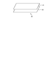
- FIG. 3 is a diagram schematically illustrating an arrangement of the first chip and the second chip according to the first embodiment.
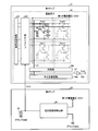
- FIG. 4 is a schematic diagram illustrating a configuration of a main part of the image sensor and the voltage conversion control circuit according to the first embodiment.
- FIG. 5 is a diagram illustrating a detailed configuration of the voltage conversion control circuit according to the first embodiment.
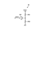
- FIG. 6 is a diagram illustrating a circuit configuration of the voltage comparison unit according to the first embodiment.
- FIG. 7 is a diagram illustrating a circuit configuration of a voltage comparison unit according to the second embodiment.
- FIG. 8 is a block diagram showing a functional configuration of the endoscope system according to the third embodiment.
- FIG. 9 is a diagram illustrating a circuit configuration of a third power supply voltage generation unit according to the third embodiment.
- FIG. 10 is a block diagram showing a functional configuration of the endoscope system according to Embodiment 4.
- FIG. 11 is a diagram illustrating a circuit configuration of a fourth power supply voltage generation unit according to the fourth embodiment.
- an endoscope system including an endoscope having an imaging device at a distal end portion of an insertion unit inserted into a subject will be described. explain. Further, the present disclosure is not limited by the embodiments. Further, in the description of the drawings, the same parts will be described with the same reference numerals. Furthermore, the drawings are schematic, and it should be noted that the relationship between the thickness and width of each member, the ratio of each member, and the like are different from reality. In addition, the drawings include portions having different dimensions and ratios.
- FIG. 1 is a schematic diagram schematically showing the entire configuration of the endoscope system according to the first embodiment.
- the endoscope system 1 illustrated in FIG. 1 includes an endoscope 2, a transmission cable 3, a connector unit 5, a processor 6, a display device 7, and a light source device 8.
- the endoscope 2 captures an image of the inside of the subject by inserting the insertion section 100, which is a part of the transmission cable 3, into the body cavity of the subject, and outputs an image signal to the processor 6. Further, the endoscope 2 is located at one end of the transmission cable 3 and at the distal end 101 side of the insertion section 100 which is inserted into the body cavity of the subject, for imaging the inside of the subject to generate a video signal.
- An apparatus 20 is provided. Further, the endoscope 2 is provided with an operation unit 4 that receives various operations on the endoscope 2 on the proximal end 102 side of the insertion unit 100.
- the video signal of the in-vivo image captured by the imaging device 20 is output to the connector unit 5 via the transmission cable 3 having a length of several meters, for example.
- the transmission cable 3 connects the endoscope 2 with the connector unit 5 and also connects the endoscope 2 with the processor 6 and the light source device 8.
- the transmission cable 3 transmits an image signal generated by the imaging device 20 to the connector unit 5.
- the transmission cable 3 is configured using a cable, an optical fiber, or the like.
- the connector unit 5 is connected to the endoscope 2, the processor 6, and the light source device 8, performs predetermined signal processing on a video signal output from the connected endoscope 2, and outputs the processed signal to the processor 6.
- the processor 6 performs predetermined image processing on the video signal input from the connector unit 5 and outputs the processed video signal to the display device 7. Further, the processor 6 controls the entire endoscope system 1 overall. For example, the processor 6 performs control to switch the illumination light emitted by the light source device 8 and to switch the imaging mode of the endoscope 2.
- the display device 7 displays an image corresponding to the video signal on which the processor 6 has performed the image processing. In addition, the display device 7 displays various information related to the endoscope system 1.
- the display device 7 is configured using a display panel such as a liquid crystal or an organic EL (Electro Luminescence).
- the light source device 8 irradiates illumination light from the distal end portion 101 side of the insertion section 100 of the endoscope 2 toward the subject via the connector section 5 and the transmission cable 3.
- the light source device 8 is configured using a white LED (Light Emitting Diode) that emits white light.
- a simultaneous illumination system is used for the light source device 8, but a field sequential illumination system may be used.
- FIG. 2 is a block diagram illustrating a functional configuration of a main part of the endoscope system 1.
- the endoscope 2 illustrated in FIG. 2 includes an imaging device 20, a transmission cable 3, and a connector unit 5.
- the imaging device 20 includes a first chip 21 and a second chip 22. As shown in FIG. 3, the imaging device 20 has a first chip 21 stacked on a second chip 22 and bonded to each other by Cu—Cu bonding or the like. The chips are connected to each other by pads arranged on the peripheral portion of each chip or vias penetrating between the chips.
- the first chip 21 and the second chip 22 are not limited to being arranged so that their main surfaces are parallel to each other, but may be arranged side by side or may be arranged with respect to one main surface to the other depending on the surrounding structure. May be stacked and arranged such that the main surfaces of the layers are vertical.
- the first chip 21 includes an image sensor 23 and a timing generator 24.
- the image sensor 23 performs photoelectric conversion by receiving a subject image condensed by an optical system (not shown), and generates an image signal by the photoelectric conversion.
- the image sensor 23 includes a plurality of pixels that generate an image signal corresponding to the amount of received light, which are arranged in a two-dimensional matrix in a matrix direction.
- the imaging element 23 is configured using an image sensor such as a CCD (Charge Coupled Device) or a CMOS (Complementary Metal Oxide Semiconductor).
- the image sensor 23 is driven by a power supply voltage VDD input from the processor 6 via the transmission cable 3 and a second power supply voltage VLO input from a second chip 22 described later.
- the power supply voltage VDD and the first power supply voltage VDD1 are the same. The detailed configuration of the image sensor 23 will be described later.
- the timing generation unit 24 generates a drive signal for driving the image sensor 23 and a voltage conversion control circuit 25 of the second chip 22, which will be described later, based on the reference clock signal CLK and the synchronization signal SYNC input from the transmission cable 3. Generate.
- the timing generator 24 outputs a drive signal to the image sensor 23 and the voltage conversion control circuit 25.
- the timing generator 24 is configured using a timing generator or the like.
- the second chip 22 has a voltage conversion control circuit 25, a capacitor 26, and a buffer unit 27.
- the voltage conversion control circuit 25 converts the voltage of the first power supply voltage VDD ⁇ b> 1 input from the processor 6 via the transmission cable 3 under the control of the timing generation unit 24, thereby converting the second power supply voltage VLO ( Negative voltage).
- the voltage conversion control circuit 25 outputs the second power supply voltage VLO to the image sensor 23 of the first chip 21.
- the detailed configuration of the voltage conversion control circuit 25 will be described later.
- the capacitor 26 has one end connected to the ground voltage GND and the other end connected to a signal line connecting the voltage conversion control circuit 25 and the first chip 21.
- the capacitor 26 functions as an external capacitor for stabilizing the second power supply voltage VLO supplied by the voltage conversion control circuit 25.
- the buffer unit 27 amplifies the image signal input from the image sensor 23 and outputs the amplified signal to the transmission cable 3.
- the buffer unit 27 is configured using an output amplifier and the like.
- the transmission cable 3 is configured using a plurality of signal lines and a light guide (not shown).
- the transmission cable 3 includes a ground line 30 for transmitting the ground voltage GND, a signal line 31 for transmitting the power supply voltage VDD (first power supply voltage VDD1), and a signal line 32 for transmitting the synchronization signal SYNC. , A signal line 33 for transmitting the reference clock signal CLK, and a signal line 34 for transmitting the image signal.
- the connector unit 5 includes an analog front end unit 51 (hereinafter, referred to as “AFE unit 51”), a signal processing unit 52, and a drive signal generation unit 53.
- AFE unit 51 analog front end unit 51
- the signal processing unit 52 and the drive signal generation unit 53 are realized using, for example, an FPGA (Field Programmable Gate Array).
- the AFE unit 51 performs processing such as noise removal and A / D conversion on the image signal transmitted from the transmission cable 3 and outputs a digital image signal to the signal processing unit 52.
- the signal processing unit 52 performs predetermined signal processing, for example, format conversion processing and gain-up processing on the digital image signal input from the AFE unit 51, and outputs the processed signal to the processor 6.
- the drive signal generator 53 generates a reference clock signal CLK and a synchronization signal SYNC for driving the imaging device 20 based on the clock signal input from the processor 6.
- the drive signal generator 53 outputs the reference clock signal CLK and the synchronization signal SYNC to the transmission cable 3.
- the processor 6 includes a power supply 61, a clock generation unit 62, an image processing unit 63, and a control unit 64.
- the power supply 61 generates a first power supply voltage VDD1 based on the ground voltage GND based on power input from the outside.
- the power supply 61 outputs the first power supply voltage VDD ⁇ b> 1 and the ground voltage GND to the transmission cable 3, and also outputs to each unit configuring the processor 6.
- the clock generation unit 62 generates a clock signal as a reference for operation of each unit of the endoscope system 1, and outputs the clock signal to the drive signal generation unit 53 of the connector unit 5 and to the control unit 64.
- the clock generator 62 is configured using a clock module or the like.
- the image processing unit 63 performs predetermined image processing on the image signal input from the signal processing unit 52 of the connector unit 5 and outputs the image signal to the display device 7 under the control of the control unit 64.
- the predetermined image processing includes, for example, white balance adjustment processing and demozaking processing.
- the image processing unit 63 is configured using a GPU (Graphics Processing Unit), an FPGA, or the like.
- the control unit 64 controls each unit of the endoscope system 1.
- the control unit 64 is configured using a CPU (Central Processing Unit), a memory, and the like.
- FIG. 4 is a schematic diagram illustrating a configuration of a main part of the image sensor 23 and the voltage conversion control circuit 25.
- the imaging element 23 includes a plurality of pixels Pxl11, Pxl12, Pxl21, Pxl22, a vertical scanning circuit 241, a level shift unit 242, a column circuit 243, a horizontal scanning circuit 244, and an output amplifier 245.
- the imaging element 23 includes a plurality of pixels Pxl11, Pxl12, Pxl21, Pxl22, a vertical scanning circuit 241, a level shift unit 242, a column circuit 243, a horizontal scanning circuit 244, and an output amplifier 245.
- four 2 ⁇ 2 pixels Pxl11, Pxl12, Pxl21, and Pxl22 are described for simplicity, but a plurality of such pixels are arranged in a two-dimensional matrix. Since the four pixels Pxl11, Pxl12, Pxl21, Pxl22 have the same configuration, the pixel Pxl21 will be described below. When any one of the four pixels Pxl11, Pxl12, Pxl21, Pxl22 is indicated, it
- the pixel Pxl21 has a photodiode PD, a transfer transistor M1, a floating region FD, an amplification transistor M2, a reset transistor M3, and a row selection transistor M4.
- the photodiode PD receives the input light and accumulates the signal light by performing photoelectric conversion into a signal charge amount corresponding to the received light amount.
- the photodiode PD has a cathode connected to the transfer transistor M1, and an anode connected to the ground voltage GND.
- the transfer transistor M1 transfers signal charges from the photodiode PD to the floating region FD.
- the transfer transistor M1 has a gate connected to a signal line to which a transfer signal is supplied, one end connected to the photodiode PD, and the other end connected to the floating region FD.
- the transfer transistor M1 is turned on when the voltage level of the transfer signal input from the vertical scanning circuit 241 and the level shift unit 242 described later becomes a high state, and transfers the signal charge from the photodiode PD to the floating region FD.
- the transfer transistor M1 is turned off when the voltage level of the transfer signal input from the vertical scanning circuit 241 and the level shift unit 242 described later becomes a low state, and the photodiode PD accumulates electric charge.
- the voltage level in the high state becomes the first power supply voltage VDD1
- the voltage level in the low state becomes the second power supply voltage VLO.
- the floating region FD converts signal charges accumulated in the photodiode PD into a voltage.
- the floating region FD includes a floating diffusion capacitance.
- the amplification transistor M2 amplifies the signal converted by the floating region FD and outputs the amplified signal to the row selection transistor M4.
- the amplification transistor M2 has a gate connected to the floating region FD, one end connected to the first power supply voltage VDD1, and the other end connected to the row selection transistor M4.
- the reset transistor M3 resets the floating region FD to a predetermined potential.
- the reset transistor M3 has a gate connected to a signal line to which a transfer signal is supplied, one end connected to the first power supply voltage VDD1, and connected to a gate of the amplification transistor M2.
- the reset transistor M3 is turned on when the voltage level of a transfer signal input from a vertical scanning circuit 241 and a level shift unit 242, which will be described later, becomes a high state, and the signal charge accumulated in the floating region FD is turned into a first power supply. By releasing the voltage to the voltage VDD1, the floating region FD is reset to a predetermined potential. When the voltage level of the transfer signal goes low, the reset transistor M3 is turned off, and the floating region FD can accumulate signal charges.
- the row selection transistor M4 transfers the signal input from the amplification transistor M2 to the vertical transfer line L1.
- the row selection transistor M4 has a gate connected to a signal line to which a column selection signal is supplied, one end connected to the amplification transistor M2, and the other end connected to the vertical transfer line L1.
- the row selection transistor M4 is turned on when the voltage level of the column selection signal input from the vertical scanning circuit 241 and the level shift unit 242, which will be described later, becomes High, and the signal input from the amplification transistor M2 is transferred to the vertical transfer line L1. Transfer to
- the vertical scanning circuit 241 supplies various signals including a transfer signal or a selection signal to a signal line of a selected pixel row of the pixel Pxl under the control of the timing generation unit 24, thereby transmitting an image signal or the like to the vertical transfer line. Output to L1.
- the vertical scanning circuit 241 is configured using, for example, an address decoder.
- the level shift unit 242 shifts various signals input from the vertical scanning circuit 241 to voltage levels necessary for driving the transistors constituting each pixel Pxl, and outputs the signals.
- the level shift unit 242 is configured using a level shift circuit.
- the column circuit 243 performs a process of canceling a characteristic variation of each pixel Pxl and removing noise on an image signal transferred from the vertical transfer line L1 based on a signal input from the horizontal scanning circuit 244. Output to the transfer line L2.
- the column circuit 243 is configured using, for example, a plurality of transistors and the like.
- the horizontal scanning circuit 244 performs a selection operation of selecting the column circuits 243 in a predetermined order under the control of the timing generation unit 24, thereby sequentially outputting image signals from the respective pixel columns to the output amplifier 245.
- the horizontal scanning circuit 244 is configured using, for example, a shift register and an address decoder.
- the output amplifier 245 amplifies the image signal input from the horizontal transfer line L2 and outputs it to the second chip 22.
- the output amplifier 245 is configured using an amplification amplifier, for example, an operational amplifier.
- the voltage conversion control circuit 25 converts the second power supply voltage VLO by converting the voltage of the first power supply voltage VDD1 input from the processor 6 via the transmission cable 3 under the control of the timing generation unit 24. Generate. Voltage conversion control circuit 25 outputs second power supply voltage VLO to level shift section 242.
- FIG. 5 is a diagram showing a detailed configuration of the voltage conversion control circuit 25.
- the voltage conversion control circuit 25 illustrated in FIG. 5 includes a booster circuit 210, a clock buffer 220, a voltage comparison unit 230, and switches SW1, SW2, and SW3.
- the switches SW1 to SW3 are configured using, for example, transistors.
- the booster circuit 210 receives a boosted clock and a voltage of a predetermined level, and increases (boosts) the absolute value of the voltage of the predetermined level to generate a second power supply voltage VLO having a negative voltage lower than the ground voltage GND. Generate.
- the booster circuit 210 is a charge pump type booster circuit configured using capacitors C1 to C4 and diodes D1 to D5.
- the clock buffer 220 drives the pumping capacitor of the booster circuit 210. Specifically, based on the drive clock signal CK1 and the drive clock signal CK2 input from the timing generator 24, a boost clock is generated, the boost clock is output to the boost circuit 210, and the second power supply voltage Hold VLO. Further, the clock buffer 220 has a first buffer circuit 221 to which the driving clock signal CK1 is input, and a second buffer circuit 222 to which the driving clock signal CK2 is input.
- the first buffer circuit 221 has one end connected to the switch SW2 and the other end connected to the capacitor C1 and the capacitor C3.
- the second buffer circuit 222 has one end connected to the switch SW3 and the other end connected to the capacitor C2 and the capacitor C4.
- the voltage comparison unit 230 detects the output voltage level of the booster circuit 210, and controls on / off of the switches SW2 and SW3 based on the detection result, thereby driving the drive clock signal CK1 supplied to the clock buffer 220. ,
- the voltage comparison section 230 includes a first voltage generation circuit 231, a second voltage generation circuit 232, and a comparator 233.
- FIG. 6 is a diagram illustrating a circuit configuration of the voltage comparison unit 230.
- the first voltage generation circuit 231 has at least one resistor between the first power supply voltage VDD1 and the second power supply voltage VLO which is a boosted voltage.
- the first voltage generation circuit 231 has a resistor R1 and a resistor R2.
- the resistors R1 and R2 are provided between a first terminal of the first power supply voltage VDD1 and a second terminal of the second power supply voltage VLO.
- the resistor R1 and the resistor R2 electrically connect the first terminal and the second terminal, and divide the voltage difference between the first power supply voltage VDD1 and the second power supply voltage VLO with a suitable voltage level.
- a first signal level-shifted to a certain first voltage level V1 is generated.
- the first voltage level V1 can be represented by the following (1).
- V1 (R2 / (R1 + R2)) ⁇ (VDD1-VLO) + VLO (1)
- the second voltage generation circuit 232 has at least one resistor between the first power supply voltage VDD1 and the ground voltage GND (ground voltage VSS).
- the second voltage generation circuit 212 has a resistor R11 and a resistor R12.
- the resistors R11 and R12 are provided between the first terminal of the first power supply voltage VDD1 and the ground terminal of the ground voltage GND.
- the combined resistance value of the resistors R11 and R12 is equal to or more than a predetermined multiple of the combined resistance value of the resistors R1 and R2.
- the combined resistance value of the resistors R11 and R12 is at least 1/10 of the combined resistance value of the resistors R1 and R2.
- the comparator 233 includes a first signal having a first voltage level V1 input from the first voltage generation circuit 231 and a second signal having a second voltage level V2 input from the second voltage generation circuit 232. And outputs the comparison result to the switches SW1 and SW2. Specifically, when the first signal of the first voltage level V1 is higher than the second signal of the second voltage level V2, the comparator 233 outputs a signal in a High state, and outputs the first voltage level. When the first signal of V1 is equal to or lower than the second signal of the second voltage level V2, a signal in a low state is output. Thus, each of the first voltage V1 and the second voltage V2 has a fluctuation component in phase with the fluctuation component ( ⁇ VDD1) of the first power supply voltage VDD1. As a result, PSRP with respect to the first power supply voltage VDD1 can be improved.
- the switch SW1 fixes the second power supply voltage VLO output from the booster circuit 210, thereby setting the second power supply voltage VLO output from the booster circuit 210.
- the power supply voltage VLO is stabilized.
- the standby mode means that the first power supply voltage VDD1 itself is supplied to a subsequent circuit, for example, the first chip 21 by stopping the operation of the voltage conversion control circuit 25. By stopping the operation of 25, the power supply to the subsequent circuit is cut off.
- PSRR is generated by generating the second voltage V2 based on the ground voltage GND and the first power supply voltage VDD1 supplied from the processor 6 via the transmission cable 3.
- the fluctuation of the first voltage level V1 and the fluctuation of the second voltage level V2 according to the fluctuation of the first power supply voltage VDD1 can be made substantially the same.
- the second voltage level V2 configured using the output voltage from the bandgap reference circuit is compared with the first power supply voltage VDD1 and the first voltage level V1 that changes according to the boosted voltage.
- the fluctuation of the first voltage level V1 in accordance with the fluctuation of the first power supply voltage VDD1 is much larger than the fluctuation of the second voltage level V2, and the PSRR is greatly deteriorated.
- Embodiment 2 is different in configuration from voltage comparing section 230 according to Embodiment 1 described above.
- the configuration of the voltage comparison unit according to the second embodiment will be described.
- the same components as those of the endoscope system 1 according to Embodiment 1 described above are denoted by the same reference numerals, and detailed description will be omitted.
- FIG. 7 is a diagram illustrating a circuit configuration of a voltage comparison unit according to the second embodiment. 7 includes a first voltage generation circuit 231A instead of the first voltage generation circuit 231 of the voltage comparison unit 230 according to Embodiment 1 described above.
- the first voltage generation circuit 231A includes a switch SW100 between the first terminal of the first power supply voltage VDD1 and the resistor R1 in addition to the configuration of the first voltage generation circuit 231 according to the first embodiment. Having.
- the switch SW100 is configured using, for example, a PMOS transistor.
- the switch SW100 is turned on during the boosting period of the boosting circuit 210 based on a signal input from the timing generation unit 24, and is turned off during the other periods. Accordingly, unnecessary fluctuation of the first voltage level (V1) due to a leak current during periods other than the boosting period of the booster circuit 210 can be suppressed.
- the boosting period is a blanking period of the image sensor 23, and the other periods are periods during which the image sensor 23 outputs image signals.
- switch SW100 is turned on (blanking period) during the boosting period of boosting circuit 210 based on the signal input from timing generation unit 24, and is turned off during the other periods. Accordingly, unnecessary fluctuation of the first voltage level (V1) due to a leak current during periods other than the boosting period of the booster circuit 210 can be suppressed.
- the switch SW100 is provided between the first terminal of the first power supply voltage VDD1 and the resistor R1.
- the switch SW100 is provided between the second terminal of the second power supply voltage VLO and the resistor R2. May be provided between them.
- Embodiment 3 has a different configuration from the endoscope system 1 according to Embodiment 1 described above.
- the configuration of the endoscope system according to Embodiment 3 will be described.
- the same components as those of the endoscope system 1 according to Embodiment 1 described above are denoted by the same reference numerals, and detailed description will be omitted.
- FIG. 8 is a block diagram showing a functional configuration of the endoscope system according to the third embodiment.
- An endoscope system 1B shown in FIG. 8 includes an endoscope 2B instead of the endoscope 2 according to the first embodiment.
- the endoscope 2B includes an imaging device 20B instead of the imaging device 20 according to Embodiment 1 described above.
- the imaging device 20B includes a second chip 22B instead of the second chip 22 according to Embodiment 1 described above.
- the second chip 22B further includes a third power supply voltage generator 28 in addition to the configuration of the second chip 22 according to the first embodiment.
- the third power supply voltage generator 28 is configured to generate a third power supply voltage VDD that is lower than the power supply voltage VDD (in the third embodiment, the same as the first power supply voltage VDD1) input from the processor 6 by a predetermined voltage.
- VDD3 the power supply voltage of the power supply voltage VDD3 (VDD1> VDD3), and this third power supply voltage VDD3 is output to some circuits constituting the voltage conversion control circuit 25.
- FIG. 9 is a diagram showing a circuit configuration of the third power supply voltage generation unit 28.
- the third power supply voltage generation unit 28 includes a resistor R31 and a resistor R32 provided between a first terminal of the first power supply voltage VDD1 and a ground terminal of the ground voltage GND. Further, the third power supply voltage generator 28 has a buffer 281.
- the third power supply voltage generation unit 28 is configured such that the resistance R31 and the resistance R32 divide the voltage difference between the first power supply voltage VDD1 and the ground voltage GND by resistance, and amplify the resistance-divided voltage by the buffer 281 to obtain the third power supply voltage.
- the generated third power supply VDD3 is used, for example, as a power supply for the comparator 233.
- the transistor capable of operating even when the first chip 21 operates at any voltage difference among the first power supply voltage VDD1, the ground voltage GND, and the second power supply voltage VLO.
- the semiconductor process used for manufacturing the second chip 22B can only provide a transistor with a withstand voltage between the first power supply voltage VDD1 and the ground voltage GND.
- the third power supply voltage generation unit 28 since the third power supply voltage generation unit 28 generates the third power supply voltage VDD3 lower than the first power supply voltage VDD1 by a predetermined voltage, the voltage conversion control can be performed without using a high withstand voltage semiconductor process.
- the circuit 25 can be provided on the second chip 22B.
- Embodiment 4 has a different configuration from the endoscope system 1B according to Embodiment 3 described above.
- the configuration of the endoscope system according to Embodiment 4 will be described.
- the same components as those of the endoscope system 1B according to Embodiment 3 described above are denoted by the same reference numerals, and detailed description thereof will be omitted.
- FIG. 10 is a block diagram showing a functional configuration of the endoscope system according to Embodiment 4.
- An endoscope system 1C shown in FIG. 10 includes an endoscope 2C instead of the endoscope 2B according to the third embodiment described above.
- the endoscope 2C includes an imaging device 20C instead of the imaging device 20B according to Embodiment 3 described above.
- imaging device 20C includes a second chip 22C instead of second chip 22B according to the third embodiment described above.
- the second chip 22C further includes a fourth power supply voltage generator 29 in addition to the configuration of the second chip 22 according to the first embodiment.
- the fourth power supply voltage generator 29 is a first power supply that is lower by a predetermined voltage than the power supply voltage VDD (the fourth power supply voltage VDD4 in the fourth embodiment) input from the processor 6 via the transmission cable 3. It generates a voltage VDD1 (VDD4> VDD1) and outputs the first power supply voltage VDD1 to the voltage conversion control circuit 25.
- FIG. 11 is a diagram showing a circuit configuration of the fourth power supply voltage generation unit 29.
- the fourth power supply voltage generation unit 29 includes a resistor R41 and a resistor R42 provided between a first terminal of the fourth power supply voltage VDD4 and a ground terminal of the ground voltage GND. Further, the fourth power supply voltage generation unit 29 includes a buffer 291.
- the fourth power supply voltage generation unit 29 is configured such that the resistances R41 and R42 divide the voltage difference between the fourth power supply voltage VDD4 and the ground voltage GND by resistance, and amplify the resistance-reduced voltage by the buffer 291 to obtain the first power supply voltage.
- the power supply voltage VDD1 is generated.
- the first chip 21 operates regardless of any voltage difference between the power supply voltage VDD (the fourth power supply voltage VDD4), the ground voltage GND, and the second power supply voltage VLO.
- the semiconductor process used for manufacturing the second chip 22C is a transistor having a withstand voltage between the fourth power supply voltage VDD4 and the ground voltage GND, and Even when only a resistance element (capacitance element) can be provided, since the fourth power supply voltage generation unit 29 generates the first power supply voltage VDD1 lower than the fourth power supply voltage VDD4 by a predetermined voltage, the fourth power supply voltage VDD1 is high.
- the voltage conversion control circuit 25 can be provided on the second chip 22C without using a withstand voltage semiconductor process.
- control device and the light source device are separate bodies, but may be formed integrally.
- the endoscope system is used.
- a video microscope for imaging a subject a mobile phone having an imaging function, and a tablet terminal having an imaging function may be used. Can be applied.
- the endoscope system provided with a flexible endoscope was used.
- an endoscope system provided with a hard endoscope and an industrial endoscope are used.
- the present invention can be applied to an endoscope system provided.
- the endoscope system including the endoscope to be inserted into the subject is used.
- the present invention can also be applied to endoscopes and endoscope systems such as electric scalpels and inspection probes.
- the “unit” described above can be read as “means” or “circuit”.
- the control unit can be read as a control unit or a control circuit.
Landscapes
- Engineering & Computer Science (AREA)
- Physics & Mathematics (AREA)
- Multimedia (AREA)
- Signal Processing (AREA)
- Optics & Photonics (AREA)
- Health & Medical Sciences (AREA)
- Life Sciences & Earth Sciences (AREA)
- Power Engineering (AREA)
- Astronomy & Astrophysics (AREA)
- General Physics & Mathematics (AREA)
- Surgery (AREA)
- Pathology (AREA)
- Molecular Biology (AREA)
- Radiology & Medical Imaging (AREA)
- Biophysics (AREA)
- Biomedical Technology (AREA)
- Heart & Thoracic Surgery (AREA)
- Medical Informatics (AREA)
- Nuclear Medicine, Radiotherapy & Molecular Imaging (AREA)
- Animal Behavior & Ethology (AREA)
- General Health & Medical Sciences (AREA)
- Public Health (AREA)
- Veterinary Medicine (AREA)
- Endoscopes (AREA)
- Transforming Light Signals Into Electric Signals (AREA)
Abstract
小型化を図ることができる撮像装置および内視鏡を提供する。電圧変換制御回路25は、昇圧回路210と、クロックバッファ220と、第1の電源電圧と第2の電源電圧とに基づいて、第1の電圧レベルの第1の信号を生成する第1の電圧生成回路231と、第1の電源電圧とグランド電圧とに基づいて、第2の電圧レベルの第2の信号を生成する第2の電圧生成回路232と、第1の電圧レベルと第2の電圧レベルとを比較し、この比較結果に基づいて、クロックバッファ220へ供給される駆動クロック信号の入力を制御する比較器233と、を含む電圧比較部230と、を有する。
Description
本開示は、被検体に挿入されることによって画像信号を生成する撮像装置および内視鏡に関する。
従来、チャージポンプ型昇圧回路は、例えばフラッシュメモリへのデータの書き込み、またはデータの消去用の電圧を発生させるため、或いは、ビデオカメラまたはデジタルカメラ等の液晶表示用の高電圧発生回路で使用されている。このチャージポンプ型昇圧回路は、1つのキャパシタとダイオード等で構成されるポンピングパケットを複数段、直列に接続し、各ポンピングパケットの昇圧により、例えばLSIチップの電源電圧よりも高い電圧を発生するものである。例えば特許文献1の電圧供給回路は、外部電源電圧を昇圧する昇圧回路と、昇圧回路から出力される昇圧電圧レベルを検出する電圧比較器と、昇圧回路に駆動用クロックを供給することによって電圧を所定レベルに保持するクロックバッファと、電圧検出部による検出結果に応じてクロックバッファのクロック入力を制御する制御回路と、を設けることによって、低消費電力、かつノイズ発生を低減している(特許文献1参照)。
ところで、内視鏡では、患者等の被検体の負担を軽減するため、被検体に挿入する挿入部の先端部に配置した撮像装置の小型化を行うことによって、挿入部の細径化を図っている。しかしながら、上述した特許文献1の電圧供給回路は、大きな面積を有するので、挿入部の先端部に配置した撮像装置の小型化を行うことが困難であった。
本開示は、上記に鑑みてなされたものであって、小型化を図ることができる撮像装置および内視鏡を提供することを目的とする。
上述した課題を解決し、目的を達成するために、本開示に係る撮像装置は、グランド電圧および前記グランド電圧より高い電圧を有する第1の電源電圧と外部から供給される駆動クロック信号とに基づいて、前記グランド電圧より低い負電圧を有する第2の電源電圧を生成する電圧変換制御回路を備え、前記電圧変換制御回路は、入力される昇圧クロック信号に基づいて、外部から入力される所定レベルの電圧を絶対値レベルで昇圧することによって前記第2の電源電圧を生成する昇圧回路と、前記第2の電源電圧を所定のレベルで保持し、かつ、前記駆動クロック信号に基づいて、前記昇圧クロック信号を生成し、該昇圧クロック信号を前記昇圧回路へ出力するクロックバッファと、前記第1の電源電圧と前記第2の電源電圧とに基づいて、第1の電圧レベルの第1の信号を生成する第1の電圧生成回路と、前記第1の電源電圧と前記グランド電圧とに基づいて、第2の電圧レベルの第2の信号を生成する第2の電圧生成回路と、前記第1の電圧レベルと前記第2の電圧レベルとを比較し、該比較結果に基づいて、前記クロックバッファへ供給される前記駆動クロック信号の入力を制御する比較器と、を含む電圧比較器と、を有する。
また、本開示に係る撮像装置は、上記開示において、前記第1の電圧生成回路は、前記第1の電源電圧の第1の端子と前記第2の電源電圧の第2の端子との間に設けられ、前記第1及び第2の端子を電気的に接続し、前記第1の電源電圧と前記第2の電源電圧の電圧差を抵抗分圧することによって前記第1の信号を出力する複数の第1の抵抗素子と、前記複数の第1の抵抗素子が前記第1の端子および前記第2の端子を電気的に接続する伝送路上に設けられ、かつ、当該撮像装置が出力する画像信号のブランキング期間においてオン状態となることによって前記複数の第1の抵抗素子を通電状態とするスイッチ素子と、を有し、前記第2の電圧生成回路は、前記第1の電源電圧の前記第1の端子と前記グランド電圧のグランド端子との間に設けられ、前記第1の端子と前記グランド端子を電気的に接続し、前記第1の電源電圧と前記グランド電圧の電圧差を抵抗分圧することによって前記第2の信号を出力する複数の第2の抵抗素子である。
また、本開示に係る撮像装置は、上記開示において、前記複数の第1の抵抗素子および前記複数の第2の抵抗素子は、同一種類の抵抗素子によって構成され、前記複数の第2の抵抗素子の合成抵抗値は、前記複数の第1の抵抗素子の合成抵抗値の所定倍以上である。
また、本開示に係る撮像装置は、上記開示において、光を受光することによって光電変換を行うことによって画像信号を生成する撮像素子を有する第1チップと、前記第1の電源電圧と前記グランド電圧とに基づいて、前記第1の電源電圧より所定の電圧だけ低い電圧を有する第3の電源電圧を生成する第3の電源電圧生成部と、前記電圧変換制御回路と、を有する第2チップと、を備え、前記電圧変換制御回路は、前記第1の電源電圧と前記グランド電圧との間の電圧で動作可能であり、かつ、前記第3の電源電圧によって動作するトランジスタをさらに有し、前記第1チップは、前記第2チップに積層されて形成されてなる。
また、本開示に係る撮像装置は、上記開示において、前記所定の電圧は、前記グランド電圧と前記第2の電源電圧との電圧差以上である。
また、本開示に係る撮像装置は、上記開示において、光を受光することによって光電変換を行うことによって画像信号を生成する撮像素子を有する第1チップと、第4の電源電圧と前記グランド電圧とに基づいて、前記第4の電源電圧より所定の電圧だけ低い前記第1の電源電圧を生成する第4の電源電圧生成部と、前記電圧変換制御回路と、を有する第2チップと、を備え、前記電圧変換制御回路は、前記第4の電源電圧と前記グランド電圧との間の電圧で動作可能であり、かつ、前記第1の電源電圧によって動作するトランジスタおよび抵抗素子を有し、前記第1チップは、前記第2チップに積層されて形成されてなる。
また、本開示に係る撮像装置は、上記開示において、前記所定の電圧は、前記グランド電圧と前記第2の電源電圧との電圧差以上である。
また、本開示に係る内視鏡は、被検体に挿入される挿入部と、前記挿入部の先端部に設けられ、前記被検体を撮像することによって画像信号を生成する撮像装置と、前記挿入部の基端側に設けられ、グランド電圧、該グランド電圧より高い電圧を有する第1の電源電圧、および駆動クロック信号を供給するプロセッサに着脱自在に接続されるコネクタ部と、を備え、前記撮像装置は、前記第1の電源電圧と前記駆動クロック信号とに基づいて、前記グランド電圧より低い負電圧を有する第2の電源電圧を生成する電圧変換制御回路を備え、前記電圧変換制御回路は、入力される昇圧クロック信号に基づいて、外部から入力される所定レベルの電圧を絶対値レベルで昇圧することによって前記第2の電源電圧を生成する昇圧回路と、前記第2の電源電圧を所定のレベルで保持し、かつ、前記駆動クロック信号に基づいて、前記昇圧クロック信号を生成し、該昇圧クロック信号を前記昇圧回路へ出力するクロックバッファと、前記第1の電源電圧と前記第2の電源電圧とに基づいて、第1の電圧レベルの第1の信号を生成する第1の電圧生成回路と、前記第1の電源電圧と前記グランド電圧とに基づいて、第2の電圧レベルの第2の信号を生成する第2の電圧生成回路と、前記第1の電圧レベルと前記第2の電圧レベルとを比較し、該比較結果に基づいて、前記クロックバッファへ供給される前記駆動クロック信号の入力を制御する比較器と、を含む電圧比較器と、を有する。
本開示によれば、小型化を図ることができるという効果を奏する。
以下、本開示を実施するための形態(以下、「実施の形態」という)として、被検体内に挿入される挿入部の先端部に撮像装置を有する内視鏡を備えた内視鏡システムについて説明する。また、この実施の形態により、本開示が限定されるものではない。さらに、図面の記載において、同一の部分には同一の符号を付して説明する。さらにまた、図面は、模式的なものであり、各部材の厚みと幅との関係、各部材の比率等は、現実と異なることに留意する必要がある。また、図面の相互間において、互いの寸法や比率が異なる部分が含まれている。
(実施の形態1)
〔内視鏡システムの構成〕
図1は、実施の形態1に係る内視鏡システムの全体構成を模式的に示す概略図である。図1に示す内視鏡システム1は、内視鏡2と、伝送ケーブル3と、コネクタ部5と、プロセッサ6と、表示装置7と、光源装置8と、を備える。
〔内視鏡システムの構成〕
図1は、実施の形態1に係る内視鏡システムの全体構成を模式的に示す概略図である。図1に示す内視鏡システム1は、内視鏡2と、伝送ケーブル3と、コネクタ部5と、プロセッサ6と、表示装置7と、光源装置8と、を備える。
内視鏡2は、伝送ケーブル3の一部である挿入部100を被検体の体腔内に挿入することによって被検体の体内を撮像して撮像信号をプロセッサ6へ出力する。また、内視鏡2は、伝送ケーブル3の一端側であり、被検体の体腔内に挿入される挿入部100の先端部101側に、被検体の体内を撮像して映像信号を生成する撮像装置20が設けられている。さらに、内視鏡2は、挿入部100の基端部102側に、内視鏡2に対する各種操作を受け付ける操作部4が設けられている。撮像装置20が撮像した体内画像の映像信号は、例えば数mの長さを有する伝送ケーブル3を経由してコネクタ部5に出力される。
伝送ケーブル3は、内視鏡2とコネクタ部5とを接続するとともに、内視鏡2とプロセッサ6および光源装置8とを接続する。また、伝送ケーブル3は、撮像装置20が生成した撮像信号をコネクタ部5へ伝送する。伝送ケーブル3は、ケーブルや光ファイバ等を用いて構成される。
コネクタ部5は、内視鏡2、プロセッサ6および光源装置8に接続され、接続された内視鏡2が出力する映像信号に所定の信号処理を施してプロセッサ6へ出力する。
プロセッサ6は、コネクタ部5から入力された映像信号に所定の画像処理を施して表示装置7へ出力する。また、プロセッサ6は、内視鏡システム1全体を統括的に制御する。例えば、プロセッサ6は、光源装置8が出射する照明光を切り替えたり、内視鏡2の撮像モードを切り替えたりする制御を行う。
表示装置7は、プロセッサ6が画像処理を施した映像信号に対応する画像を表示する。また、表示装置7は、内視鏡システム1に関する各種情報を表示する。表示装置7は、液晶や有機EL(Electro Luminescence)等の表示パネル等を用いて構成される。
光源装置8は、コネクタ部5および伝送ケーブル3を経由して内視鏡2の挿入部100の先端部101側から被検体(被写体)に向けて照明光を照射する。光源装置8は、白色光を発する白色LED(Light Emitting Diode)等を用いて構成される。なお、本実施の形態では、光源装置8に同時方式の照明方式が採用されるが、面順次方式の照明方式であってもよい。
〔内視鏡システムの要部〕
次に、内視鏡システム1の要部の機能について説明する。図2は、内視鏡システム1の要部の機能構成を示すブロック図である。
次に、内視鏡システム1の要部の機能について説明する。図2は、内視鏡システム1の要部の機能構成を示すブロック図である。
〔内視鏡の構成〕
まず、内視鏡2の構成について説明する。
図2に示す内視鏡2は、撮像装置20と、伝送ケーブル3と、コネクタ部5と、を備える。
まず、内視鏡2の構成について説明する。
図2に示す内視鏡2は、撮像装置20と、伝送ケーブル3と、コネクタ部5と、を備える。
撮像装置20は、第1チップ21と、第2チップ22と、を有する。撮像装置20は、図3に示すように、第2チップ22に第1チップ21が積層され、Cu-Cu接合等によって相対して貼り合わされる。また、チップ間は、各チップの周縁部に配置されるパッド、またはチップ間を貫通するビア等により接続される。なお、第1チップ21および第2チップ22は、双方の主面が平行になるように配置するものに限らず、周囲の構造により、横に並べて配置したり、一方の主面に対して他方の主面が垂直になるように積層して配置したりしてもよい。
まず、第1チップ21について説明する。
第1チップ21は、撮像素子23と、タイミング生成部24と、を有する。
第1チップ21は、撮像素子23と、タイミング生成部24と、を有する。
撮像素子23は、図示しない光学系が集光した被写体像を受光することによって光電変換を行い、この光電変換によって画像信号を生成する。撮像素子23は、受光量に応じた画像信号を生成する複数の画素が行列方向に二次元マトリクス状に配置されてなる。撮像素子23は、CCD(Charge Coupled Device)やCMOS(Complementary Metal Oxide Semiconductor)等のイメージセンサを用いて構成される。また、撮像素子23は、伝送ケーブル3を経由してプロセッサ6から入力される電源電圧VDDおよび後述する第2チップ22から入力される第2の電源電圧VLOによって駆動する。実施の形態1では、電源電圧VDDと第1の電源電圧VDD1は同じである。なお、撮像素子23の詳細な構成は後述する。
タイミング生成部24は、伝送ケーブル3から入力される基準クロック信号CLKおよび同期信号SYNCに基づいて、撮像素子23および後述する第2チップ22の電圧変換制御回路25等を駆動するための駆動信号を生成する。タイミング生成部24は、駆動信号を撮像素子23および電圧変換制御回路25へ出力する。タイミング生成部24は、タイミングジェネレータ等を用いて構成される。
次に、第2チップ22について説明する。
第2チップ22は、電圧変換制御回路25と、コンデンサ26と、バッファ部27と、を有する。
第2チップ22は、電圧変換制御回路25と、コンデンサ26と、バッファ部27と、を有する。
電圧変換制御回路25は、タイミング生成部24の制御のもと、伝送ケーブル3を経由してプロセッサ6から入力される第1の電源電圧VDD1の電圧を変換することによって第2の電源電圧VLO(負電圧)を生成する。電圧変換制御回路25は、第2の電源電圧VLOを第1チップ21の撮像素子23へ出力する。なお、電圧変換制御回路25の詳細な構成については後述する。
コンデンサ26は、一端がグランド電圧GNDに接続され、他端が電圧変換制御回路25と第1チップ21とを接続する信号線に接続される。コンデンサ26は、電圧変換制御回路25が供給する第2の電源電圧VLOを安定化させるための外付け容量として機能する。
バッファ部27は、撮像素子23から入力された画像信号の増幅を行って伝送ケーブル3へ出力する。バッファ部27は、出力アンプ等を用いて構成される。
〔伝送ケーブルの構成〕
次に、伝送ケーブル3について説明する。
伝送ケーブル3は、複数の信号線および図示しないライトガイドを用いて構成される。具体的には、伝送ケーブル3は、グランド電圧GNDを伝送するグランド線30と、電源電圧VDD(第1の電源電圧VDD1)を伝送する信号線31と、同期信号SYNCを伝送する信号線32と、基準クロック信号CLKを伝送する信号線33と、画像信号を伝送する信号線34と、を有する。
次に、伝送ケーブル3について説明する。
伝送ケーブル3は、複数の信号線および図示しないライトガイドを用いて構成される。具体的には、伝送ケーブル3は、グランド電圧GNDを伝送するグランド線30と、電源電圧VDD(第1の電源電圧VDD1)を伝送する信号線31と、同期信号SYNCを伝送する信号線32と、基準クロック信号CLKを伝送する信号線33と、画像信号を伝送する信号線34と、を有する。
〔コネクタ部の構成〕
次に、コネクタ部5の構成について説明する。
コネクタ部5は、アナログ・フロント・エンド部51(以下、「AFE部51」という)と、信号処理部52と、駆動信号生成部53と、を有する。なお、AFE部51、信号処理部52および駆動信号生成部53は、例えばFPGA(Field Programmable Gate Array)を用いて実現される。
次に、コネクタ部5の構成について説明する。
コネクタ部5は、アナログ・フロント・エンド部51(以下、「AFE部51」という)と、信号処理部52と、駆動信号生成部53と、を有する。なお、AFE部51、信号処理部52および駆動信号生成部53は、例えばFPGA(Field Programmable Gate Array)を用いて実現される。
AFE部51は、伝送ケーブル3から伝送された画像信号に対してノイズ除去およびA/D変換等の処理を行ってデジタルの画像信号を信号処理部52へ出力する。
信号処理部52は、AFE部51から入力されたデジタルの画像信号に対して所定の信号処理、例えばフォーマット変換処理やゲインアップ処理等を行ってプロセッサ6へ出力する。
駆動信号生成部53は、プロセッサ6から入力されるクロック信号に基づいて、撮像装置20を駆動するための基準クロック信号CLKおよび同期信号SYNCを生成する。駆動信号生成部53は、基準クロック信号CLKおよび同期信号SYNCを伝送ケーブル3へ出力する。
〔プロセッサの構成〕
次に、プロセッサ6の構成について説明する。
プロセッサ6は、電源61と、クロック生成部62と、画像処理部63と、制御部64と、を備える。
次に、プロセッサ6の構成について説明する。
プロセッサ6は、電源61と、クロック生成部62と、画像処理部63と、制御部64と、を備える。
電源61は、外部から入力された電力に基づいて、グランド電圧GNDを基準とした第1の電源電圧VDD1を生成する。電源61は、第1の電源電圧VDD1およびグランド電圧GNDを伝送ケーブル3へ出力するとともに、プロセッサ6を構成する各部へ出力する。
クロック生成部62は、内視鏡システム1の各部の動作の基準となるクロック信号を生成し、このクロック信号をコネクタ部5の駆動信号生成部53へ出力するとともに、制御部64へ出力する。クロック生成部62は、クロック・モジュール等を用いて構成される。
画像処理部63は、制御部64の制御のもと、コネクタ部5の信号処理部52から入力された画像信号に対して、所定の画像処理を行って表示装置7へ出力する。ここで、所定の画像処理としては、例えばホワイトバランス調整処理およびデモザキング処理等である。画像処理部63は、GPU(Graphics Processing Unit)やFPGA等を用いて構成される。
制御部64は、内視鏡システム1の各部を制御する。制御部64は、CPU(Central Processing Unit)およびメモリ等を用いて構成される。
〔撮像素子および電圧変換制御回路の構成〕
次に、上述した撮像素子23および電圧変換制御回路25の要部の構成について説明する。図4は、撮像素子23および電圧変換制御回路25の要部の構成を示す模式図である。
次に、上述した撮像素子23および電圧変換制御回路25の要部の構成について説明する。図4は、撮像素子23および電圧変換制御回路25の要部の構成を示す模式図である。
〔撮像素子〕
まず、撮像素子23の構成について説明する。図4に示すように、撮像素子23は、複数の画素Pxl11,Pxl12,Pxl21,Pxl22と、垂直走査回路241と、レベルシフト部242と、列回路243と、水平走査回路244と、出力アンプ245と、を有する。なお、図4では、説明を簡略するため、2×2の4つの画素Pxl11,Pxl12,Pxl21,Pxl22について説明するが、このような画素が2次元マトリクス状に複数配置されている。なお、4つの画素Pxl11,Pxl12,Pxl21,Pxl22の各々は、同様の構成のため、以下においては、画素Pxl21について説明する。また、4つの画素Pxl11,Pxl12,Pxl21,Pxl22のいずれか1つを指す場合、単に画素Pxlと表現する。
まず、撮像素子23の構成について説明する。図4に示すように、撮像素子23は、複数の画素Pxl11,Pxl12,Pxl21,Pxl22と、垂直走査回路241と、レベルシフト部242と、列回路243と、水平走査回路244と、出力アンプ245と、を有する。なお、図4では、説明を簡略するため、2×2の4つの画素Pxl11,Pxl12,Pxl21,Pxl22について説明するが、このような画素が2次元マトリクス状に複数配置されている。なお、4つの画素Pxl11,Pxl12,Pxl21,Pxl22の各々は、同様の構成のため、以下においては、画素Pxl21について説明する。また、4つの画素Pxl11,Pxl12,Pxl21,Pxl22のいずれか1つを指す場合、単に画素Pxlと表現する。
画素Pxl21は、フォトダイオードPDと、転送トランジスタM1と、フローティングディージョンFDと、増幅トランジスタM2と、リセットトランジスタM3と、行選択トランジスタM4と、を有する。
フォトダイオードPDは、入力光を受光し、受光した受光量に応じた信号電荷量に光電変換を行うことによって蓄積する。フォトダイオードPDは、カソード側が転送トランジスタM1に接続され、アノード側がグランド電圧GNDに接続される。
転送トランジスタM1は、フォトダイオードPDからフローティングディージョンFDへ信号電荷を転送する。転送トランジスタM1は、ゲートに転送信号が供給される信号線が接続され、一端側にフォトダイオードPDが接続され、他端側にフローティングディージョンFDが接続される。転送トランジスタM1は、後述する垂直走査回路241およびレベルシフト部242から入力される転送信号の電圧レベルがHigh状態となると、オン状態となり、フォトダイオードPDからフローティングディージョンFDに信号電荷を転送する。また、転送トランジスタM1は、後述する垂直走査回路241およびレベルシフト部242から入力される転送信号の電圧レベルがLow状態となると、オフ状態となり、フォトダイオードPDが電荷を蓄積する。なお、転送信号は、High状態の電圧レベルが第1の電源電圧VDD1となり、Low状態の電圧レベルが第2の電源電圧VLOとなる。
フローティングディージョンFDは、フォトダイオードPDに蓄積された信号電荷を電圧に変換する。フローティングディージョンFDは、浮遊拡散容量からなる。
増幅トランジスタM2は、フローティングディージョンFDによって変換された信号を増幅して行選択トランジスタM4へ出力する。増幅トランジスタM2は、ゲートにフローティングディージョンFDが接続され、一端側が第1の電源電圧VDD1に接続され、他端側が行選択トランジスタM4に接続される。
リセットトランジスタM3は、フローティングディージョンFDを所定電位にリセットする。リセットトランジスタM3は、ゲートに転送信号が供給される信号線が接続され、一端側に第1の電源電圧VDD1が接続され、増幅トランジスタM2のゲートに接続される。リセットトランジスタM3は、後述する垂直走査回路241およびレベルシフト部242から入力される転送信号の電圧レベルがHigh状態となると、オン状態となり、フローティングディージョンFDに蓄積された信号電荷を第1の電源電圧VDD1に放出させることによってフローティングディージョンFDを所定電位にリセットする。リセットトランジスタM3は、転送信号の電圧レベルがLow状態となると、オフ状態となり、フローティングディージョンFDが信号電荷を蓄積可能な状態となる。
行選択トランジスタM4は、増幅トランジスタM2から入力された信号を垂直転送線L1へ転送する。行選択トランジスタM4は、ゲートに列選択信号が供給される信号線が接続され、一端側が増幅トランジスタM2に接続され、他端側が垂直転送線L1に接続される。行選択トランジスタM4は、後述する垂直走査回路241およびレベルシフト部242から入力される列選択信号の電圧レベルがHigh状態となると、オン状態となり、増幅トランジスタM2から入力された信号を垂直転送線L1へ転送する。
垂直走査回路241は、タイミング生成部24の制御のもと、画素Pxlの選択された画素行の信号線に転送信号または選択信号を含む各種信号を供給することによって、画像信号等を垂直転送線L1へ出力させる。垂直走査回路241は、例えばアドレスデコーダ等を用いて構成される。
レベルシフト部242は、垂直走査回路241から入力された各種信号を、各画素Pxlを構成する各トランジスタの駆動に必要な電圧レベルにシフトすることによって出力する。レベルシフト部242は、レベルシフト回路を用いて構成される。
列回路243は、水平走査回路244から入力される信号に基づいて、垂直転送線L1から転送された画像信号に対して、各画素Pxlの特性ばらつきの相殺やノイズを除去する処理を行って水平転送線L2へ出力する。列回路243は、例えば複数のトランジスタ等を用いて構成される。
水平走査回路244は、タイミング生成部24の制御のもと、列回路243を所定の順番で選択する選択操作を行うことによって、各画素列から画像信号を出力アンプ245に順次出力させる。水平走査回路244は、例えばシフトレジスタおよびアドレスデコーダ等を用いて構成される。
出力アンプ245は、水平転送線L2から入力された画像信号を増幅することによって第2チップ22へ出力する。出力アンプ245は、増幅アンプ、例えばオペアンプ等を用いて構成される。
〔電圧変換制御回路〕
次に、電圧変換制御回路25の構成について説明する。
電圧変換制御回路25は、タイミング生成部24の制御のもと、伝送ケーブル3を経由してプロセッサ6から入力される第1の電源電圧VDD1の電圧を変換することによって第2の電源電圧VLOを生成する。電圧変換制御回路25は、第2の電源電圧VLOをレベルシフト部242へ出力する。
次に、電圧変換制御回路25の構成について説明する。
電圧変換制御回路25は、タイミング生成部24の制御のもと、伝送ケーブル3を経由してプロセッサ6から入力される第1の電源電圧VDD1の電圧を変換することによって第2の電源電圧VLOを生成する。電圧変換制御回路25は、第2の電源電圧VLOをレベルシフト部242へ出力する。
図5は、電圧変換制御回路25の詳細な構成を示す図である。図5に示す電圧変換制御回路25は、昇圧回路210と、クロックバッファ220と、電圧比較部230と、スイッチSW1、スイッチSW2、スイッチSW3と、を有する。なお、スイッチSW1~SW3は、例えばトランジスタを用いて構成される。
昇圧回路210は、昇圧クロックと所定レベルの電圧が入力され、この所定のレベルの電圧の絶対値を増大(昇圧)することによって、グランド電圧GNDより低い負電圧を有する第2の電源電圧VLOを生成する。昇圧回路210は、キャパシタC1~キャパシタC4と、ダイオードD1~ダイオードD5と、を用いて構成されたチャージポンプ型昇圧回路である。
クロックバッファ220は、昇圧回路210のポンピングキャパシタを駆動する。具体的には、タイミング生成部24から入力される駆動クロック信号CK1,駆動クロック信号CK2に基づいて、昇圧クロックを生成し、この昇圧クロックを昇圧回路210へ出力し、かつ、第2の電源電圧VLOを保持する。さらに、クロックバッファ220は、駆動クロック信号CK1が入力される第1のバッファ回路221と、駆動クロック信号CK2が入力される第2のバッファ回路222と、を有する。
第1のバッファ回路221は、一端側がスイッチSW2に接続され、他端側がキャパシタC1およびキャパシタC3に接続される。
第2のバッファ回路222は、一端側がスイッチSW3に接続され、他端側がキャパシタC2およびキャパシタC4に接続される。
電圧比較部230は、昇圧回路210の出力電圧レベルを検出し、この検出結果に基づいて、スイッチSW2,スイッチSW3のオンまたはオフを制御することによって、クロックバッファ220に供給される駆動クロック信号CK1,駆動クロック信号CK2を制御する。電圧比較部230は、第1の電圧生成回路231と、第2の電圧生成回路232と、比較器233と、を有する。
図6は、電圧比較部230の回路構成を示す図である。図6に示すように、第1の電圧生成回路231は、第1の電源電圧VDD1と昇圧電圧である第2の電源電圧VLOとの間に少なくとも一つの抵抗を有する。具体的には、第1の電圧生成回路231は、抵抗R1および抵抗R2を有する。抵抗R1および抵抗R2は、第1の電源電圧VDD1の第1の端子と第2の電源電圧VLOの第2の端子との間に設けられる。抵抗R1および抵抗R2は、第1の端子および第2の端子を電気的に接続し、第1の電源電圧VDD1と第2の電源電圧VLOの電圧差を抵抗分圧することによって好適な電圧レベルである第1の電圧レベルV1にレベルシフトした第1の信号を生成する。具体的には、以下の(1)によって、第1の電圧レベルV1を表すことができる。
V1=(R2/(R1+R2))×(VDD1-VLO)+VLO ・・・(1)
V1=(R2/(R1+R2))×(VDD1-VLO)+VLO ・・・(1)
第2の電圧生成回路232は、第1の電源電圧VDD1とグランド電圧GND(グランド電圧VSS)との間に少なくとも1つの抵抗を有する。具体的には、第2の電圧生成回路212は、抵抗R11および抵抗R12を有する。抵抗R11および抵抗R12は、第1の電源電圧VDD1の第1の端子とグランド電圧GNDのグランド端子との間に設けられている。また、抵抗R11および抵抗R12の合成抵抗値は、抵抗R1および抵抗R2の合成抵抗値の所定倍以上である。具体的には、抵抗R11および抵抗R12の合成抵抗値は、抵抗R1および抵抗R2の合成抵抗値の1/10以上である。さらに、抵抗R1、抵抗R2および抵抗R11および抵抗R12は、同一種類の抵抗素子によって構成される。また、抵抗R11および抵抗R12は、第1の端子およびグランド端子を電気的に接続し、第1の電源電圧VDD1とグランド電圧GNDの電圧差を抵抗分圧することによって好適な電圧レベルである第2の電圧レベルV2にレベルシフトした第2の信号を生成する。具体的には、以下の(2)によって、第2の電圧レベルV2を表すことができる。
V2=(R12/(R11+R12))×(VDD1-VSS)+VSS ・・(2)
V2=(R12/(R11+R12))×(VDD1-VSS)+VSS ・・(2)
比較器233は、第1の電圧生成回路231から入力される第1の電圧レベルV1の第1の信号と第2の電圧生成回路232から入力される第2の電圧レベルV2の第2の信号とを比較し、この比較結果をスイッチSW1およびスイッチSW2へ出力する。具体的には、比較器233は、第1の電圧レベルV1の第1の信号が第2の電圧レベルV2の第2の信号より高い場合、High状態の信号を出力し、第1の電圧レベルV1の第1の信号が第2の電圧レベルV2の第2の信号以下の場合、Low状態の信号を出力する。これにより、第1の電圧V1および第2の電圧V2の各々は、第1の電源電圧VDD1の変動成分(ΔVDD1)と同相な変動成分を有する。この結果、第1の電源電圧VDD1に対するPSRPを向上させることができる。
図5に戻り、電圧変換制御回路25の構成について説明する。
スイッチSW1は、タイミング生成部24からスタンバイモードを設定するスタンバイ信号STBYが入力された場合、昇圧回路210が出力する第2の電源電圧VLOを固定することによって、昇圧回路210が出力する第2の電源電圧VLOを安定化させる。ここで、スタンバイモードとは、電圧変換制御回路25の動作を停止することによって、後段の回路、例えば第1チップ21に、第1の電源電圧VDD1自体が供給されているが、電圧変換制御回路25の動作を停止することによって後段の回路への電源供給を遮断することである。
スイッチSW1は、タイミング生成部24からスタンバイモードを設定するスタンバイ信号STBYが入力された場合、昇圧回路210が出力する第2の電源電圧VLOを固定することによって、昇圧回路210が出力する第2の電源電圧VLOを安定化させる。ここで、スタンバイモードとは、電圧変換制御回路25の動作を停止することによって、後段の回路、例えば第1チップ21に、第1の電源電圧VDD1自体が供給されているが、電圧変換制御回路25の動作を停止することによって後段の回路への電源供給を遮断することである。
以上説明した実施の形態1によれば、伝送ケーブル3を経由してプロセッサ6から供給されるグランド電圧GNDと第1の電源電圧VDD1に基づいて、第2の電圧V2を生成することによって、PSRRの高い負電圧VLOを簡易な構成で生成することができるので、撮像装置20の小型化を図ることができる。
また、実施の形態1によれば、第1の電源電圧VDD1の変動に応じた第1の電圧レベルV1の変動と第2の電圧レベルV2の変動とを略同様にすることが可能であるので、昇圧電圧を所定の電圧レベルに保持することが容易となる。これに対して、例えばバンドギャップレファレンス回路からの出力電圧を用いて構成した第2の電圧レベルV2を、第1の電源電圧VDD1および昇圧電圧に応じて変化する第1の電圧レベルV1と比較する場合、第1の電源電圧VDD1の変動に応じた第1の電圧レベルV1の変動が第2の電圧レベルV2の変動と比較して非常に大きくなり、PSRRが大幅に劣化する。
(実施の形態2)
次に、実施の形態2について説明する。実施の形態2は、上述した実施の形態1に係る電圧比較部230と構成が異なる。以下においては、実施の形態2に係る電圧比較部の構成について説明する。なお、上述した実施の形態1に係る内視鏡システム1と同一の構成には同一の符号を付して詳細な説明を省略する。
次に、実施の形態2について説明する。実施の形態2は、上述した実施の形態1に係る電圧比較部230と構成が異なる。以下においては、実施の形態2に係る電圧比較部の構成について説明する。なお、上述した実施の形態1に係る内視鏡システム1と同一の構成には同一の符号を付して詳細な説明を省略する。
〔電圧比較部の構成〕
図7は、実施の形態2に係る電圧比較部の回路構成を示す図である。図7に示す電圧比較部230Aは、上述した実施の形態1に係る電圧比較部230の第1の電圧生成回路231に換えて、第1の電圧生成回路231Aを備える。
図7は、実施の形態2に係る電圧比較部の回路構成を示す図である。図7に示す電圧比較部230Aは、上述した実施の形態1に係る電圧比較部230の第1の電圧生成回路231に換えて、第1の電圧生成回路231Aを備える。
第1の電圧生成回路231Aは、上述した実施の形態1に係る第1の電圧生成回路231の構成に加えて、第1の電源電圧VDD1の第1の端子と抵抗R1との間にスイッチSW100を有する。
スイッチSW100は、例えばPMOSトランジスタを用いて構成される。スイッチSW100は、タイミング生成部24から入力される信号に基づいて、昇圧回路210の昇圧期間にON状態となり、それ以外の期間がオフ状態となる。これにより、昇圧回路210の昇圧期間以外におけるリーク電流による第1の電圧レベル(V1)の不要な変動を抑制することができる。ここで、昇圧期間とは、撮像素子23のブランキング期間であり、それ以外の期間とは、撮像素子23が画像信号を出力している期間である。
以上説明した実施の形態2によれば、スイッチSW100がタイミング生成部24から入力される信号に基づいて、昇圧回路210の昇圧期間にON状態(ブランキング期間)となり、それ以外の期間がオフ状態となることによって、昇圧回路210の昇圧期間以外におけるリーク電流による第1の電圧レベル(V1)の不要な変動を抑制することができる。
なお、実施の形態2では、スイッチSW100を第1の電源電圧VDD1の第1の端子と抵抗R1との間に設けていたが、例えば第2の電源電圧VLOの第2の端子と抵抗R2との間に設けてもよい。
(実施の形態3)
次に、実施の形態3について説明する。実施の形態3は、上述した実施の形態1に係る内視鏡システム1と構成が異なる。以下においては、実施の形態3に係る内視鏡システムの構成について説明する。なお、上述した実施の形態1に係る内視鏡システム1と同一の構成には同一の符号を付して詳細な説明を省略する。
次に、実施の形態3について説明する。実施の形態3は、上述した実施の形態1に係る内視鏡システム1と構成が異なる。以下においては、実施の形態3に係る内視鏡システムの構成について説明する。なお、上述した実施の形態1に係る内視鏡システム1と同一の構成には同一の符号を付して詳細な説明を省略する。
〔内視鏡システムの構成〕
図8は、実施の形態3に係る内視鏡システムの機能構成を示すブロック図である。図8に示す内視鏡システム1Bは、上述した実施の形態1に係る内視鏡2に換えて、内視鏡2Bを備える。また、内視鏡2Bは、上述した実施の形態1に係る撮像装置20に換えて、撮像装置20Bを備える。さらに、撮像装置20Bは、上述した実施の形態1に係る第2チップ22に換えて、第2チップ22Bを備える。
図8は、実施の形態3に係る内視鏡システムの機能構成を示すブロック図である。図8に示す内視鏡システム1Bは、上述した実施の形態1に係る内視鏡2に換えて、内視鏡2Bを備える。また、内視鏡2Bは、上述した実施の形態1に係る撮像装置20に換えて、撮像装置20Bを備える。さらに、撮像装置20Bは、上述した実施の形態1に係る第2チップ22に換えて、第2チップ22Bを備える。
第2チップ22Bは、上述した実施の形態1に係る第2チップ22の構成に加えて、第3の電源電圧生成部28をさらに備える。
第3の電源電圧生成部28は、伝送ケーブル3を経由してプロセッサ6から入力された電源電圧VDD(実施の形態3では、第1の電源電圧VDD1と同じ)から所定の電圧だけ低い第3の電源電圧VDD3(VDD1>VDD3)を生成し、この第3の電源電圧VDD3は電圧変換制御回路25を構成する一部の回路に出力される。
図9は、第3の電源電圧生成部28の回路構成を示す図である。図9に示すように、第3の電源電圧生成部28は、第1の電源電圧VDD1の第1の端子とグランド電圧GNDのグランド端子との間に抵抗R31および抵抗R32が設けられている。さらに、第3の電源電圧生成部28は、バッファ281を有する。第3の電源電圧生成部28は、抵抗R31および抵抗R32が第1の電源電圧VDD1とグランド電圧GNDの電圧差を抵抗分圧し、この抵抗分圧した電圧をバッファ281によって増幅することによって第3の電源電圧VDD3を生成する。この生成された第3の電源VDD3は、例えば比較器233の電源として用いる。
以上説明した実施の形態3によれば、第1チップ21が第1の電源電圧VDD1、グランド電圧GNDおよび第2の電源電圧VLOの何れの電圧差であっても動作することが可能なトランジスタを設ける比較的高耐圧な半導体プロセスを用いて製造される場合において、第2チップ22Bの製造に用いる半導体プロセスが第1の電源電圧VDD1とグランド電圧GND間程度の耐圧のトランジスタしか設けることができないときであっても、第3の電源電圧生成部28が第1の電源電圧VDD1から所定の電圧だけ低い第3の電源電圧VDD3を生成するので、高耐圧な半導体プロセスを用いることなく、電圧変換制御回路25を第2チップ22B上に設けることができる。
(実施の形態4)
次に、実施の形態4について説明する。実施の形態4は、上述した実施の形態3に係る内視鏡システム1Bと構成が異なる。以下においては、実施の形態4に係る内視鏡システムの構成について説明する。なお、上述した実施の形態3に係る内視鏡システム1Bと同一の構成には同一の符号を付して詳細な説明を省略する。
次に、実施の形態4について説明する。実施の形態4は、上述した実施の形態3に係る内視鏡システム1Bと構成が異なる。以下においては、実施の形態4に係る内視鏡システムの構成について説明する。なお、上述した実施の形態3に係る内視鏡システム1Bと同一の構成には同一の符号を付して詳細な説明を省略する。
図10は、実施の形態4に係る内視鏡システムの機能構成を示すブロック図である。図10に示す内視鏡システム1Cは、上述した実施の形態3に係る内視鏡2Bに換えて、内視鏡2Cを備える。また、内視鏡2Cは、上述した実施の形態3に係る撮像装置20Bに換えて、撮像装置20Cを備える。さらに、撮像装置20Cは、上述した実施の形態3に係る第2チップ22Bに換えて、第2チップ22Cを備える。
第2チップ22Cは、上述した実施の形態1に係る第2チップ22の構成に加えて、第4の電源電圧生成部29をさらに備える。
第4の電源電圧生成部29は、伝送ケーブル3を経由してプロセッサ6から入力された電源電圧VDD(実施の形態4では、第4の電源電圧VDD4)から所定の電圧だけ低い第1の電源電圧VDD1(VDD4>VDD1)を生成し、第1の電源電圧VDD1を電圧変換制御回路25へ出力する。
図11は、第4の電源電圧生成部29の回路構成を示す図である。図11に示すように、第4の電源電圧生成部29は、第4の電源電圧VDD4の第1の端子とグランド電圧GNDのグランド端子との間に抵抗R41および抵抗R42が設けられている。さらに、第4の電源電圧生成部29は、バッファ291を有する。第4の電源電圧生成部29は、抵抗R41および抵抗R42が第4の電源電圧VDD4とグランド電圧GNDの電圧差を抵抗分圧し、この抵抗番圧した電圧をバッファ291によって増幅することによって第1の電源電圧VDD1を生成する。
以上説明した実施の形態4によれば、第1チップ21が電源電圧VDD(第4の電源電圧VDD4)、グランド電圧GNDおよび第2の電源電圧VLOの何れの電圧差であっても動作することが可能なトランジスタを設ける比較的高耐圧な半導体プロセスを用いて製造される場合において、第2チップ22Cの製造に用いる半導体プロセスが第4の電源電圧VDD4とグランド電圧GND間程度の耐圧のトランジスタおよび抵抗素子(容量素子)しか設けることができないときであっても、第4の電源電圧生成部29が第4の電源電圧VDD4から所定の電圧だけ低い第1の電源電圧VDD1を生成するので、高耐圧な半導体プロセスを用いることなく、電圧変換制御回路25を第2チップ22C上に設けることができる。
(その他の実施の形態)
上述した本開示の実施の形態1~4に開示されている複数の構成要素を適宜組み合わせることによって、種々の発明を形成することができる。例えば、上述した本開示の実施の形態1~4に記載した全構成要素からいくつかの構成要素を削除してもよい。さらに、上述した本開示の実施の形態1~4で説明した構成要素を適宜組み合わせてもよい。
上述した本開示の実施の形態1~4に開示されている複数の構成要素を適宜組み合わせることによって、種々の発明を形成することができる。例えば、上述した本開示の実施の形態1~4に記載した全構成要素からいくつかの構成要素を削除してもよい。さらに、上述した本開示の実施の形態1~4で説明した構成要素を適宜組み合わせてもよい。
また、本開示の実施の形態1~4では、制御装置と光源装置とが別体であったが、一体的に形成してもよい。
また、本開示の実施の形態1~4では、内視鏡システムであったが、例えば被検体を撮像するビデオマイクロスコープ、撮像機能を有する携帯電話および撮像機能を有するタブレット型端末であっても適用することができる。
また、本開示の実施の形態1~4では、軟性の内視鏡を備えた内視鏡システムであったが、硬性の内視鏡を備えた内視鏡システム、工業用の内視鏡を備えた内視鏡システムであっても適用することができる。
また、本開示の実施の形態1~4では、被検体に挿入される内視鏡を備えた内視鏡システムであったが、例えば硬性の内視鏡を備えた内視鏡システム、副鼻腔内視鏡および電気メスや検査プローブ等の内視鏡システムであっても適用することができる。
また、本開示の実施の形態1~4では、上述してきた「部」は、「手段」や「回路」などに読み替えることができる。例えば、制御部は、制御手段や制御回路に読み替えることができる。
以上、本願の実施の形態のいくつかを図面に基づいて詳細に説明したが、これらは例示であり、本発明の開示の欄に記載の態様を始めとして、当業者の知識に基づいて種々の変形、改良を施した他の形態で本発明を実施することが可能である。
1,1B,1C 内視鏡システム
2,2B,2C 内視鏡
3 伝送ケーブル
4 操作部
5 コネクタ部
6 プロセッサ
7 表示装置
8 光源装置
20,20B,20C 撮像装置
21 第1チップ
22,22B,22C 第2チップ
23 撮像素子
24 タイミング生成部
25 電圧変換制御回路
26 コンデンサ
27 バッファ部
28 第3の電源電圧生成部
29 第4の電源電圧生成部
51 AFE部
52 信号処理部
53 駆動信号生成部
61 電源
62 クロック生成部
63 画像処理部
64 制御部
100 挿入部
101 先端部
102 基端部
210 昇圧回路
213 比較器
220 クロックバッファ
221 第1のバッファ回路
222 第2のバッファ回路
230,230A 電圧比較部
231,231A 第1の電圧生成回路
232 第2の電圧生成回路
233 比較器
241 垂直走査回路
242 レベルシフト部
243 列回路
244 水平走査回路
245 出力アンプ
281,291 バッファ
C1~C4 キャパシタ
D1~D5 ダイオード
FD フローティングディージョン
L1 垂直転送線
L2 水平転送線
M1 転送トランジスタ
M2 増幅トランジスタ
M3 リセットトランジスタ
M4 行選択トランジスタ
PD フォトダイオード
Pxl 画素
R1,R2,R11,R12,R31,R32,R41,R42 抵抗
SW1,SW2,SW3,SW100 スイッチ
2,2B,2C 内視鏡
3 伝送ケーブル
4 操作部
5 コネクタ部
6 プロセッサ
7 表示装置
8 光源装置
20,20B,20C 撮像装置
21 第1チップ
22,22B,22C 第2チップ
23 撮像素子
24 タイミング生成部
25 電圧変換制御回路
26 コンデンサ
27 バッファ部
28 第3の電源電圧生成部
29 第4の電源電圧生成部
51 AFE部
52 信号処理部
53 駆動信号生成部
61 電源
62 クロック生成部
63 画像処理部
64 制御部
100 挿入部
101 先端部
102 基端部
210 昇圧回路
213 比較器
220 クロックバッファ
221 第1のバッファ回路
222 第2のバッファ回路
230,230A 電圧比較部
231,231A 第1の電圧生成回路
232 第2の電圧生成回路
233 比較器
241 垂直走査回路
242 レベルシフト部
243 列回路
244 水平走査回路
245 出力アンプ
281,291 バッファ
C1~C4 キャパシタ
D1~D5 ダイオード
FD フローティングディージョン
L1 垂直転送線
L2 水平転送線
M1 転送トランジスタ
M2 増幅トランジスタ
M3 リセットトランジスタ
M4 行選択トランジスタ
PD フォトダイオード
Pxl 画素
R1,R2,R11,R12,R31,R32,R41,R42 抵抗
SW1,SW2,SW3,SW100 スイッチ
Claims (8)
- グランド電圧および前記グランド電圧より高い電圧を有する第1の電源電圧と外部から供給される駆動クロック信号とに基づいて、前記グランド電圧より低い負電圧を有する第2の電源電圧を生成する電圧変換制御回路を備え、
前記電圧変換制御回路は、
入力される昇圧クロック信号に基づいて、外部から入力される所定レベルの電圧を絶対値レベルで昇圧することによって前記第2の電源電圧を生成する昇圧回路と、
前記第2の電源電圧を所定のレベルで保持し、かつ、前記駆動クロック信号に基づいて、前記昇圧クロック信号を生成し、該昇圧クロック信号を前記昇圧回路へ出力するクロックバッファと、
前記第1の電源電圧と前記第2の電源電圧とに基づいて、第1の電圧レベルの第1の信号を生成する第1の電圧生成回路と、前記第1の電源電圧と前記グランド電圧とに基づいて、第2の電圧レベルの第2の信号を生成する第2の電圧生成回路と、前記第1の電圧レベルと前記第2の電圧レベルとを比較し、該比較結果に基づいて、前記クロックバッファへ供給される前記駆動クロック信号の入力を制御する比較器と、を含む電圧比較器と、
を有する
撮像装置。 - 請求項1に記載の撮像装置であって、
前記第1の電圧生成回路は、
前記第1の電源電圧の第1の端子と前記第2の電源電圧の第2の端子との間に設けられ、前記第1及び第2の端子を電気的に接続し、前記第1の電源電圧と前記第2の電源電圧の電圧差を抵抗分圧することによって前記第1の信号を出力する複数の第1の抵抗素子と、
前記複数の第1の抵抗素子が前記第1の端子および前記第2の端子を電気的に接続する伝送路上に設けられ、かつ、当該撮像装置が出力する画像信号のブランキング期間においてオン状態となることによって前記複数の第1の抵抗素子を通電状態とするスイッチ素子と、
を有し、
前記第2の電圧生成回路は、
前記第1の電源電圧の前記第1の端子と前記グランド電圧のグランド端子との間に設けられ、前記第1の端子と前記グランド端子を電気的に接続し、前記第1の電源電圧と前記グランド電圧の電圧差を抵抗分圧することによって前記第2の信号を出力する複数の第2の抵抗素子
を有する
撮像装置。 - 請求項2に記載の撮像装置であって、
前記複数の第1の抵抗素子および前記複数の第2の抵抗素子は、同一種類の抵抗素子によって構成され、
前記複数の第2の抵抗素子の合成抵抗値は、前記複数の第1の抵抗素子の合成抵抗値の所定倍以上である
撮像装置。 - 請求項1に記載の撮像装置であって、
光を受光することによって光電変換を行うことによって画像信号を生成する撮像素子を有する第1チップと、
前記第1の電源電圧と前記グランド電圧とに基づいて、前記第1の電源電圧より所定の電圧だけ低い電圧を有する第3の電源電圧を生成する第3の電源電圧生成部と、前記電圧変換制御回路と、を有する第2チップと、
を備え、
前記電圧変換制御回路は、
前記第1の電源電圧と前記グランド電圧との間の電圧で動作可能であり、かつ、前記第3の電源電圧によって動作するトランジスタをさらに有する
撮像装置。 - 請求項4に記載の撮像装置であって、
前記所定の電圧は、
前記グランド電圧と前記第2の電源電圧との電圧差以上である
撮像装置。 - 請求項1に記載の撮像装置であって、
光を受光することによって光電変換を行うことによって画像信号を生成する撮像素子を有する第1チップと、
第4の電源電圧と前記グランド電圧とに基づいて、前記第4の電源電圧より所定の電圧だけ低い前記第1の電源電圧を生成する第4の電源電圧生成部と、前記電圧変換制御回路と、を有する第2チップと、
を備え、
前記電圧変換制御回路は、
前記第4の電源電圧と前記グランド電圧との間の電圧で動作可能であり、かつ、前記第1の電源電圧によって動作するトランジスタおよび抵抗素子を有する
撮像装置。 - 請求項6に記載の撮像装置であって、
前記所定の電圧は、
前記グランド電圧と前記第2の電源電圧との電圧差以上である
撮像装置。 - 被検体に挿入される挿入部と、
前記挿入部の先端部に設けられ、前記被検体を撮像することによって画像信号を生成する撮像装置と、
前記挿入部の基端側に設けられ、グランド電圧、前記グランド電圧より高い電圧を有する第1の電源電圧、および駆動クロック信号を供給するプロセッサに着脱自在に接続されるコネクタ部と、
を備え、
前記撮像装置は、
前記第1の電源電圧と前記駆動クロック信号とに基づいて、前記グランド電圧より低い負電圧を有する第2の電源電圧を生成する電圧変換制御回路を備え、
前記電圧変換制御回路は、
入力される昇圧クロック信号に基づいて、外部から入力される所定レベルの電圧を絶対値レベルで昇圧することによって前記第2の電源電圧を生成する昇圧回路と、
前記第2の電源電圧を所定のレベルで保持し、かつ、前記駆動クロック信号に基づいて、前記昇圧クロック信号を生成し、該昇圧クロック信号を前記昇圧回路へ出力するクロックバッファと、
前記第1の電源電圧と前記第2の電源電圧とに基づいて、第1の電圧レベルの第1の信号を生成する第1の電圧生成回路と、前記第1の電源電圧と前記グランド電圧とに基づいて、第2の電圧レベルの第2の信号を生成する第2の電圧生成回路と、前記第1の電圧レベルと前記第2の電圧レベルとを比較し、該比較結果に基づいて、前記クロックバッファへ供給される前記駆動クロック信号の入力を制御する比較器と、を含む電圧比較器と、
を有する内視鏡。
Priority Applications (1)
| Application Number | Priority Date | Filing Date | Title |
|---|---|---|---|
| US17/154,006 US11877053B2 (en) | 2018-07-23 | 2021-01-21 | Booster apparatus, imaging apparatus, endoscope and voltage conversion control method |
Applications Claiming Priority (2)
| Application Number | Priority Date | Filing Date | Title |
|---|---|---|---|
| JP2018137870 | 2018-07-23 | ||
| JP2018-137870 | 2018-07-23 |
Related Child Applications (1)
| Application Number | Title | Priority Date | Filing Date |
|---|---|---|---|
| US17/154,006 Continuation US11877053B2 (en) | 2018-07-23 | 2021-01-21 | Booster apparatus, imaging apparatus, endoscope and voltage conversion control method |
Publications (1)
| Publication Number | Publication Date |
|---|---|
| WO2020021747A1 true WO2020021747A1 (ja) | 2020-01-30 |
Family
ID=69181385
Family Applications (1)
| Application Number | Title | Priority Date | Filing Date |
|---|---|---|---|
| PCT/JP2019/006407 Ceased WO2020021747A1 (ja) | 2018-07-23 | 2019-02-20 | 撮像装置および内視鏡 |
Country Status (2)
| Country | Link |
|---|---|
| US (1) | US11877053B2 (ja) |
| WO (1) | WO2020021747A1 (ja) |
Cited By (2)
| Publication number | Priority date | Publication date | Assignee | Title |
|---|---|---|---|---|
| WO2023002566A1 (ja) * | 2021-07-20 | 2023-01-26 | オリンパスメディカルシステムズ株式会社 | 撮像装置、スコープ、および内視鏡システム |
| CN118766395A (zh) * | 2024-06-14 | 2024-10-15 | 中山市元盛电子科技有限公司 | 一种内窥镜式检查装置的fpc电路板结构 |
Families Citing this family (2)
| Publication number | Priority date | Publication date | Assignee | Title |
|---|---|---|---|---|
| CN114098606A (zh) * | 2021-11-30 | 2022-03-01 | 四川耐特光电科技有限公司 | 一种用于内窥镜一体机的电磁屏蔽电路 |
| US12273105B2 (en) * | 2022-04-28 | 2025-04-08 | Olympus Medical Systems Corp. | Voltage generation circuit, image sensor, scope, and voltage generation method |
Citations (4)
| Publication number | Priority date | Publication date | Assignee | Title |
|---|---|---|---|---|
| JPH09294367A (ja) * | 1996-04-24 | 1997-11-11 | Sony Corp | 電圧供給回路 |
| JP2003348822A (ja) * | 2002-05-28 | 2003-12-05 | Sony Corp | 電圧変換制御回路及び方法 |
| JP2005080395A (ja) * | 2003-08-29 | 2005-03-24 | Rohm Co Ltd | 電源装置 |
| JP2006129127A (ja) * | 2004-10-29 | 2006-05-18 | Olympus Corp | 電圧供給回路及びそれを用いた固体撮像装置 |
Family Cites Families (1)
| Publication number | Priority date | Publication date | Assignee | Title |
|---|---|---|---|---|
| US7239193B2 (en) * | 2003-12-25 | 2007-07-03 | Kabushiki Kaisha Toshiba | Semiconductor device |
-
2019
- 2019-02-20 WO PCT/JP2019/006407 patent/WO2020021747A1/ja not_active Ceased
-
2021
- 2021-01-21 US US17/154,006 patent/US11877053B2/en active Active
Patent Citations (4)
| Publication number | Priority date | Publication date | Assignee | Title |
|---|---|---|---|---|
| JPH09294367A (ja) * | 1996-04-24 | 1997-11-11 | Sony Corp | 電圧供給回路 |
| JP2003348822A (ja) * | 2002-05-28 | 2003-12-05 | Sony Corp | 電圧変換制御回路及び方法 |
| JP2005080395A (ja) * | 2003-08-29 | 2005-03-24 | Rohm Co Ltd | 電源装置 |
| JP2006129127A (ja) * | 2004-10-29 | 2006-05-18 | Olympus Corp | 電圧供給回路及びそれを用いた固体撮像装置 |
Cited By (3)
| Publication number | Priority date | Publication date | Assignee | Title |
|---|---|---|---|---|
| WO2023002566A1 (ja) * | 2021-07-20 | 2023-01-26 | オリンパスメディカルシステムズ株式会社 | 撮像装置、スコープ、および内視鏡システム |
| US12452557B2 (en) | 2021-07-20 | 2025-10-21 | Olympus Medical Systems Corp. | Imaging device, scope, and endoscope system |
| CN118766395A (zh) * | 2024-06-14 | 2024-10-15 | 中山市元盛电子科技有限公司 | 一种内窥镜式检查装置的fpc电路板结构 |
Also Published As
| Publication number | Publication date |
|---|---|
| US11877053B2 (en) | 2024-01-16 |
| US20210168287A1 (en) | 2021-06-03 |
Similar Documents
| Publication | Publication Date | Title |
|---|---|---|
| US11877053B2 (en) | Booster apparatus, imaging apparatus, endoscope and voltage conversion control method | |
| US9974431B2 (en) | Image sensor, imaging device, endoscope, and endoscope system | |
| US9621776B2 (en) | Imaging element, imaging device and endoscope system | |
| US9813645B2 (en) | Image sensor, imaging device, endoscope, and endoscopic system | |
| KR20160040173A (ko) | 변환 장치, 촬상 장치, 전자 기기, 변환 방법 | |
| US10506917B2 (en) | Endoscope and endoscope system with transmission buffer | |
| US20180054580A1 (en) | Image sensor and endoscope | |
| US9693002B2 (en) | Image sensor, imaging device, endoscope, and endoscope system | |
| US20180064314A1 (en) | Image sensor, endoscope, and endoscope system | |
| US12443027B2 (en) | Photoelectric conversion device, camera module, endoscope, endoscope system, and apparatus | |
| CN107251226A (zh) | 摄像元件 | |
| JP2019213120A (ja) | 映像取得装置および内視鏡 | |
| CN108141556A (zh) | 摄像元件、内窥镜以及内窥镜系统 | |
| JP6253551B2 (ja) | 撮像素子、撮像装置、内視鏡および内視鏡システム | |
| JPWO2019230063A1 (ja) | 撮像装置、撮像システムおよび撮像方法 |
Legal Events
| Date | Code | Title | Description |
|---|---|---|---|
| 121 | Ep: the epo has been informed by wipo that ep was designated in this application |
Ref document number: 19841484 Country of ref document: EP Kind code of ref document: A1 |
|
| NENP | Non-entry into the national phase |
Ref country code: DE |
|
| 122 | Ep: pct application non-entry in european phase |
Ref document number: 19841484 Country of ref document: EP Kind code of ref document: A1 |