WO2020021591A1 - Uninterruptible power supply device - Google Patents
Uninterruptible power supply device Download PDFInfo
- Publication number
- WO2020021591A1 WO2020021591A1 PCT/JP2018/027469 JP2018027469W WO2020021591A1 WO 2020021591 A1 WO2020021591 A1 WO 2020021591A1 JP 2018027469 W JP2018027469 W JP 2018027469W WO 2020021591 A1 WO2020021591 A1 WO 2020021591A1
- Authority
- WO
- WIPO (PCT)
- Prior art keywords
- power supply
- inverter
- power
- voltage
- converter
- Prior art date
Links
Images


Classifications
-
- H—ELECTRICITY
- H02—GENERATION; CONVERSION OR DISTRIBUTION OF ELECTRIC POWER
- H02J—CIRCUIT ARRANGEMENTS OR SYSTEMS FOR SUPPLYING OR DISTRIBUTING ELECTRIC POWER; SYSTEMS FOR STORING ELECTRIC ENERGY
- H02J9/00—Circuit arrangements for emergency or stand-by power supply, e.g. for emergency lighting
- H02J9/04—Circuit arrangements for emergency or stand-by power supply, e.g. for emergency lighting in which the distribution system is disconnected from the normal source and connected to a standby source
- H02J9/06—Circuit arrangements for emergency or stand-by power supply, e.g. for emergency lighting in which the distribution system is disconnected from the normal source and connected to a standby source with automatic change-over, e.g. UPS systems
- H02J9/062—Circuit arrangements for emergency or stand-by power supply, e.g. for emergency lighting in which the distribution system is disconnected from the normal source and connected to a standby source with automatic change-over, e.g. UPS systems for AC powered loads
-
- H—ELECTRICITY
- H02—GENERATION; CONVERSION OR DISTRIBUTION OF ELECTRIC POWER
- H02J—CIRCUIT ARRANGEMENTS OR SYSTEMS FOR SUPPLYING OR DISTRIBUTING ELECTRIC POWER; SYSTEMS FOR STORING ELECTRIC ENERGY
- H02J9/00—Circuit arrangements for emergency or stand-by power supply, e.g. for emergency lighting
- H02J9/04—Circuit arrangements for emergency or stand-by power supply, e.g. for emergency lighting in which the distribution system is disconnected from the normal source and connected to a standby source
- H02J9/06—Circuit arrangements for emergency or stand-by power supply, e.g. for emergency lighting in which the distribution system is disconnected from the normal source and connected to a standby source with automatic change-over, e.g. UPS systems
-
- H—ELECTRICITY
- H02—GENERATION; CONVERSION OR DISTRIBUTION OF ELECTRIC POWER
- H02M—APPARATUS FOR CONVERSION BETWEEN AC AND AC, BETWEEN AC AND DC, OR BETWEEN DC AND DC, AND FOR USE WITH MAINS OR SIMILAR POWER SUPPLY SYSTEMS; CONVERSION OF DC OR AC INPUT POWER INTO SURGE OUTPUT POWER; CONTROL OR REGULATION THEREOF
- H02M7/00—Conversion of ac power input into dc power output; Conversion of dc power input into ac power output
- H02M7/42—Conversion of dc power input into ac power output without possibility of reversal
- H02M7/44—Conversion of dc power input into ac power output without possibility of reversal by static converters
- H02M7/48—Conversion of dc power input into ac power output without possibility of reversal by static converters using discharge tubes with control electrode or semiconductor devices with control electrode
-
- H—ELECTRICITY
- H02—GENERATION; CONVERSION OR DISTRIBUTION OF ELECTRIC POWER
- H02M—APPARATUS FOR CONVERSION BETWEEN AC AND AC, BETWEEN AC AND DC, OR BETWEEN DC AND DC, AND FOR USE WITH MAINS OR SIMILAR POWER SUPPLY SYSTEMS; CONVERSION OF DC OR AC INPUT POWER INTO SURGE OUTPUT POWER; CONTROL OR REGULATION THEREOF
- H02M1/00—Details of apparatus for conversion
- H02M1/0048—Circuits or arrangements for reducing losses
-
- H—ELECTRICITY
- H02—GENERATION; CONVERSION OR DISTRIBUTION OF ELECTRIC POWER
- H02M—APPARATUS FOR CONVERSION BETWEEN AC AND AC, BETWEEN AC AND DC, OR BETWEEN DC AND DC, AND FOR USE WITH MAINS OR SIMILAR POWER SUPPLY SYSTEMS; CONVERSION OF DC OR AC INPUT POWER INTO SURGE OUTPUT POWER; CONTROL OR REGULATION THEREOF
- H02M1/00—Details of apparatus for conversion
- H02M1/36—Means for starting or stopping converters
-
- H—ELECTRICITY
- H02—GENERATION; CONVERSION OR DISTRIBUTION OF ELECTRIC POWER
- H02M—APPARATUS FOR CONVERSION BETWEEN AC AND AC, BETWEEN AC AND DC, OR BETWEEN DC AND DC, AND FOR USE WITH MAINS OR SIMILAR POWER SUPPLY SYSTEMS; CONVERSION OF DC OR AC INPUT POWER INTO SURGE OUTPUT POWER; CONTROL OR REGULATION THEREOF
- H02M3/00—Conversion of dc power input into dc power output
- H02M3/02—Conversion of dc power input into dc power output without intermediate conversion into ac
- H02M3/04—Conversion of dc power input into dc power output without intermediate conversion into ac by static converters
-
- H—ELECTRICITY
- H02—GENERATION; CONVERSION OR DISTRIBUTION OF ELECTRIC POWER
- H02M—APPARATUS FOR CONVERSION BETWEEN AC AND AC, BETWEEN AC AND DC, OR BETWEEN DC AND DC, AND FOR USE WITH MAINS OR SIMILAR POWER SUPPLY SYSTEMS; CONVERSION OF DC OR AC INPUT POWER INTO SURGE OUTPUT POWER; CONTROL OR REGULATION THEREOF
- H02M5/00—Conversion of ac power input into ac power output, e.g. for change of voltage, for change of frequency, for change of number of phases
- H02M5/40—Conversion of ac power input into ac power output, e.g. for change of voltage, for change of frequency, for change of number of phases with intermediate conversion into dc
- H02M5/42—Conversion of ac power input into ac power output, e.g. for change of voltage, for change of frequency, for change of number of phases with intermediate conversion into dc by static converters
- H02M5/44—Conversion of ac power input into ac power output, e.g. for change of voltage, for change of frequency, for change of number of phases with intermediate conversion into dc by static converters using discharge tubes or semiconductor devices to convert the intermediate dc into ac
- H02M5/453—Conversion of ac power input into ac power output, e.g. for change of voltage, for change of frequency, for change of number of phases with intermediate conversion into dc by static converters using discharge tubes or semiconductor devices to convert the intermediate dc into ac using devices of a triode or transistor type requiring continuous application of a control signal
- H02M5/458—Conversion of ac power input into ac power output, e.g. for change of voltage, for change of frequency, for change of number of phases with intermediate conversion into dc by static converters using discharge tubes or semiconductor devices to convert the intermediate dc into ac using devices of a triode or transistor type requiring continuous application of a control signal using semiconductor devices only
- H02M5/4585—Conversion of ac power input into ac power output, e.g. for change of voltage, for change of frequency, for change of number of phases with intermediate conversion into dc by static converters using discharge tubes or semiconductor devices to convert the intermediate dc into ac using devices of a triode or transistor type requiring continuous application of a control signal using semiconductor devices only having a rectifier with controlled elements
-
- H—ELECTRICITY
- H02—GENERATION; CONVERSION OR DISTRIBUTION OF ELECTRIC POWER
- H02M—APPARATUS FOR CONVERSION BETWEEN AC AND AC, BETWEEN AC AND DC, OR BETWEEN DC AND DC, AND FOR USE WITH MAINS OR SIMILAR POWER SUPPLY SYSTEMS; CONVERSION OF DC OR AC INPUT POWER INTO SURGE OUTPUT POWER; CONTROL OR REGULATION THEREOF
- H02M7/00—Conversion of ac power input into dc power output; Conversion of dc power input into ac power output
- H02M7/02—Conversion of ac power input into dc power output without possibility of reversal
- H02M7/04—Conversion of ac power input into dc power output without possibility of reversal by static converters
- H02M7/12—Conversion of ac power input into dc power output without possibility of reversal by static converters using discharge tubes with control electrode or semiconductor devices with control electrode
- H02M7/21—Conversion of ac power input into dc power output without possibility of reversal by static converters using discharge tubes with control electrode or semiconductor devices with control electrode using devices of a triode or transistor type requiring continuous application of a control signal
- H02M7/217—Conversion of ac power input into dc power output without possibility of reversal by static converters using discharge tubes with control electrode or semiconductor devices with control electrode using devices of a triode or transistor type requiring continuous application of a control signal using semiconductor devices only
- H02M7/219—Conversion of ac power input into dc power output without possibility of reversal by static converters using discharge tubes with control electrode or semiconductor devices with control electrode using devices of a triode or transistor type requiring continuous application of a control signal using semiconductor devices only in a bridge configuration
-
- H—ELECTRICITY
- H02—GENERATION; CONVERSION OR DISTRIBUTION OF ELECTRIC POWER
- H02M—APPARATUS FOR CONVERSION BETWEEN AC AND AC, BETWEEN AC AND DC, OR BETWEEN DC AND DC, AND FOR USE WITH MAINS OR SIMILAR POWER SUPPLY SYSTEMS; CONVERSION OF DC OR AC INPUT POWER INTO SURGE OUTPUT POWER; CONTROL OR REGULATION THEREOF
- H02M7/00—Conversion of ac power input into dc power output; Conversion of dc power input into ac power output
- H02M7/42—Conversion of dc power input into ac power output without possibility of reversal
- H02M7/44—Conversion of dc power input into ac power output without possibility of reversal by static converters
- H02M7/48—Conversion of dc power input into ac power output without possibility of reversal by static converters using discharge tubes with control electrode or semiconductor devices with control electrode
- H02M7/53—Conversion of dc power input into ac power output without possibility of reversal by static converters using discharge tubes with control electrode or semiconductor devices with control electrode using devices of a triode or transistor type requiring continuous application of a control signal
- H02M7/537—Conversion of dc power input into ac power output without possibility of reversal by static converters using discharge tubes with control electrode or semiconductor devices with control electrode using devices of a triode or transistor type requiring continuous application of a control signal using semiconductor devices only, e.g. single switched pulse inverters
- H02M7/5387—Conversion of dc power input into ac power output without possibility of reversal by static converters using discharge tubes with control electrode or semiconductor devices with control electrode using devices of a triode or transistor type requiring continuous application of a control signal using semiconductor devices only, e.g. single switched pulse inverters in a bridge configuration
-
- Y—GENERAL TAGGING OF NEW TECHNOLOGICAL DEVELOPMENTS; GENERAL TAGGING OF CROSS-SECTIONAL TECHNOLOGIES SPANNING OVER SEVERAL SECTIONS OF THE IPC; TECHNICAL SUBJECTS COVERED BY FORMER USPC CROSS-REFERENCE ART COLLECTIONS [XRACs] AND DIGESTS
- Y02—TECHNOLOGIES OR APPLICATIONS FOR MITIGATION OR ADAPTATION AGAINST CLIMATE CHANGE
- Y02B—CLIMATE CHANGE MITIGATION TECHNOLOGIES RELATED TO BUILDINGS, e.g. HOUSING, HOUSE APPLIANCES OR RELATED END-USER APPLICATIONS
- Y02B70/00—Technologies for an efficient end-user side electric power management and consumption
- Y02B70/10—Technologies improving the efficiency by using switched-mode power supplies [SMPS], i.e. efficient power electronics conversion e.g. power factor correction or reduction of losses in power supplies or efficient standby modes
-
- Y—GENERAL TAGGING OF NEW TECHNOLOGICAL DEVELOPMENTS; GENERAL TAGGING OF CROSS-SECTIONAL TECHNOLOGIES SPANNING OVER SEVERAL SECTIONS OF THE IPC; TECHNICAL SUBJECTS COVERED BY FORMER USPC CROSS-REFERENCE ART COLLECTIONS [XRACs] AND DIGESTS
- Y02—TECHNOLOGIES OR APPLICATIONS FOR MITIGATION OR ADAPTATION AGAINST CLIMATE CHANGE
- Y02B—CLIMATE CHANGE MITIGATION TECHNOLOGIES RELATED TO BUILDINGS, e.g. HOUSING, HOUSE APPLIANCES OR RELATED END-USER APPLICATIONS
- Y02B70/00—Technologies for an efficient end-user side electric power management and consumption
- Y02B70/30—Systems integrating technologies related to power network operation and communication or information technologies for improving the carbon footprint of the management of residential or tertiary loads, i.e. smart grids as climate change mitigation technology in the buildings sector, including also the last stages of power distribution and the control, monitoring or operating management systems at local level
-
- Y—GENERAL TAGGING OF NEW TECHNOLOGICAL DEVELOPMENTS; GENERAL TAGGING OF CROSS-SECTIONAL TECHNOLOGIES SPANNING OVER SEVERAL SECTIONS OF THE IPC; TECHNICAL SUBJECTS COVERED BY FORMER USPC CROSS-REFERENCE ART COLLECTIONS [XRACs] AND DIGESTS
- Y04—INFORMATION OR COMMUNICATION TECHNOLOGIES HAVING AN IMPACT ON OTHER TECHNOLOGY AREAS
- Y04S—SYSTEMS INTEGRATING TECHNOLOGIES RELATED TO POWER NETWORK OPERATION, COMMUNICATION OR INFORMATION TECHNOLOGIES FOR IMPROVING THE ELECTRICAL POWER GENERATION, TRANSMISSION, DISTRIBUTION, MANAGEMENT OR USAGE, i.e. SMART GRIDS
- Y04S20/00—Management or operation of end-user stationary applications or the last stages of power distribution; Controlling, monitoring or operating thereof
- Y04S20/20—End-user application control systems
Definitions
- the present invention relates to an uninterruptible power supply.
- a converter that converts AC power from an AC power supply into DC power
- an inverter that converts the DC power generated by the converter or the DC power of the power storage device into AC power and supplies the AC power to a load
- a configuration including a series circuit of a converter and an inverter and a bypass circuit connected in parallel between an AC power supply and a load has been widely adopted.
- a converter and an inverter are used during normal operation when AC power is normally supplied from the AC power supply.
- power supply is continued by the inverter.
- Such a power supply method is also called a constant inverter power supply method.
- the continuous inverter power supply method the power is supplied from the inverter to the load via the DC link both when the AC power supply is normal and during a power failure, so it is easy to ensure the power supply quality of the output regardless of the quality of the input power supply. It has excellent power supply stability.
- the always-inverter power supply system power loss occurs because energy normally passes through the converter and the inverter, and there is a problem of improving operation efficiency.
- the uninterruptible power supply normally executes bypass power supply for supplying AC power to the load from the AC power supply via the semiconductor switch which is a bypass circuit.
- the semiconductor switch a thyristor switch configured by connecting a pair of thyristors in antiparallel is used.
- the thyristor constituting the thyristor switch is turned off when the current flowing through the thyristor reaches zero. In other words, the thyristor switch remains on until the current reaches zero even after the gate signal is cut off. Therefore, even if the gate signal of the thyristor switch is cut off when the voltage drop of the AC power supply is detected, the thyristor switch is not immediately turned off depending on the timing of cutting off the gate signal, and the AC output terminal of the uninterruptible power supply is There may be a case where the state where the power supply and the AC input terminal are electrically connected via the thyristor switch continues.
- the present invention has been made to solve such a problem, and an object of the present invention is to provide an uninterruptible power supply capable of suppressing a decrease in load current when switching from the eco mode to the inverter power supply mode. To provide.
- an uninterruptible power supply connected between an AC power supply and a load, comprising a converter, an inverter, a first switch, a second switch, and a control device.
- the converter converts AC power supplied from an AC power supply into DC power in a forward manner.
- the inverter reversely converts DC power output from the converter or DC power output from the power storage device into AC power.
- the first switch is connected between the inverter and the load.
- the second switch is connected between the AC power supply and the load.
- the control device controls the converter, the inverter, the first switch, and the second switch.
- the uninterruptible power supply has a first power supply mode and a second power supply mode.
- the first power supply mode is configured to turn on the first switch and turn off the second switch to supply AC power output from the inverter to the load.
- the second power supply mode is configured to turn off the first switch and turn on the second switch to supply AC power from the AC power supply to the load.
- the control device is configured to switch to the first power supply mode when detecting a voltage drop of the AC power supply while the second power supply mode is being executed.
- the control device causes the converter to perform an inverse conversion so as to convert the DC power output from the power storage device into the AC power for a predetermined period from the time when the voltage drop of the AC power supply is detected, and also controls the AC voltage output from the converter.
- the reverse conversion in the converter is controlled so that the instantaneous value is equal to or greater than the instantaneous value of the AC voltage output from the inverter.
- an uninterruptible power supply capable of suppressing a decrease in load current when switching from the eco mode to the inverter power supply mode.
- FIG. 1 is a circuit block diagram showing a configuration of an uninterruptible power supply according to an embodiment of the present invention.
- FIG. 2 is a circuit diagram showing a main part of the uninterruptible power supply shown in FIG. 1.
- FIG. 4 is a diagram for explaining a flow of power in an eco mode.
- FIG. 4 is a diagram for describing a flow of power in an inverter power supply mode. It is a figure for explaining the flow of electric power at the time of switching from eco mode to inverter feed mode.
- FIG. 9 is a waveform diagram for explaining an operation of the uninterruptible power supply device when switching from the eco mode to the inverter power supply mode. It is a figure for explaining the flow of electric power at the time of switching from eco mode to inverter feed mode.
- FIG. 4 is a diagram for explaining a flow of power in an eco mode.
- FIG. 4 is a diagram for describing a flow of power in an inverter power supply mode. It is a figure for explaining the flow
- FIG. 9 is a waveform diagram for explaining an operation of the uninterruptible power supply device when switching from the eco mode to the inverter power supply mode. It is a block diagram for explaining the control composition of the uninterruptible power supply by a control device. It is a flowchart explaining the control processing of an uninterruptible power supply by a control apparatus.
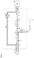
- FIG. 1 is a circuit block diagram showing a configuration of an uninterruptible power supply 1 according to an embodiment of the present invention.
- the uninterruptible power supply 1 converts the three-phase AC power from the commercial AC power supply 21 into DC power once, converts the DC power into three-phase AC power, and supplies the converted power to the load 22.
- FIG. 1 shows only a circuit corresponding to one phase (for example, the U phase) of the three phases (the U phase, the V phase, and the W phase) for simplification of the drawing and the description.
- the uninterruptible power supply 1 has an inverter power supply mode and a bypass power supply mode.
- the inverter power supply mode is an operation mode in which AC power is supplied from the inverter 10 to the load 22.
- the bypass power supply mode is an operation mode in which AC power is supplied from the commercial AC power supply 21 to the load 22 via the semiconductor switch 15.
- inverter power supply mode AC power supplied from the commercial AC power supply 21 is converted into DC power by the converter 6, and the DC power is converted into AC power by the inverter 10 and supplied to the load 22. Therefore, in the inverter power supply mode, power supply stability to the load 22 is excellent.
- the bypass power supply mode the AC power supplied from the commercial AC power supply 21 is supplied to the load 22 via the semiconductor switch 15 (second switch), in other words, without passing through the converter 6 and the inverter 10. I do. Therefore, occurrence of power loss in converter 6 and inverter 10 is suppressed, and as a result, the operation efficiency of uninterruptible power supply 1 can be improved.
- the bypass power supply mode is also referred to as an “eco mode”, which is an operation mode in which high efficiency operation of the uninterruptible power supply 1 is emphasized.
- the inverter power supply mode corresponds to the “first power supply mode”
- the bypass power supply mode (eco mode) corresponds to the “second power supply mode”.
- the uninterruptible power supply 1 includes an AC input terminal T1, an AC output terminal T2, and a battery terminal T3.
- AC input terminal T1 receives commercial frequency AC power from commercial AC power supply 21.
- the AC output terminal T2 is connected to the load 22.
- the load 22 is driven by AC power.
- Battery terminal T3 is connected to battery (power storage device) 23.
- Battery 23 stores DC power.
- a capacitor may be connected instead of the battery 23.
- the uninterruptible power supply 1 further includes electromagnetic contactors 2, 8, 14, current detectors 3, 11, capacitors 4, 9, 13, reactors 5, 12, converter 6, bidirectional chopper 7, inverter 10, and semiconductor switch. 15, an operation unit 17, and a control device 18.
- the electromagnetic contactor 2 and the reactor 5 are connected in series between the AC input terminal T1 and the input node of the converter 6.
- Capacitor 4 is connected to node N1 between electromagnetic contactor 2 and reactor 5. The electromagnetic contactor 2 is turned on when the uninterruptible power supply 1 is used, and is turned off, for example, when the uninterruptible power supply 1 is maintained.
- the instantaneous value of the AC input voltage Vin appearing at the node N1 is detected by the control device 18. Based on the instantaneous value of the AC input voltage Vin, it is determined whether or not an instantaneous voltage drop and a power failure have occurred.
- the current detector 3 detects an AC input current Iin flowing to the node N1, and supplies a signal Iin indicating the detected value to the control device 18.
- Capacitor 4 and reactor 5 constitute a low-pass filter, and pass commercial frequency AC power from commercial AC power supply 21 to converter 6, and a signal of a switching frequency generated in converter 6 passes to commercial AC power supply 21.
- the converter 6 is controlled by the control device 18 and normally converts three-phase AC power into DC power (forward conversion) and outputs the DC power to the DC line L1 when AC power is supplied from the commercial AC power supply 21. During a power outage when the supply of AC power from commercial AC power supply 21 is stopped, the operation of converter 6 is stopped. The output voltage of converter 6 can be controlled to a desired value.
- the capacitor 9 is connected to the DC line L1 and smoothes the voltage of the DC line L1.
- the instantaneous value of the DC voltage VDC appearing on the DC line L1 is detected by the control device 18.
- the DC line L1 is connected to the high-voltage node of the bidirectional chopper 7, and the low-voltage node of the bidirectional chopper 7 is connected to the battery terminal T3 via the electromagnetic contactor 8.
- the electromagnetic contactor 8 is turned on when the uninterruptible power supply 1 is used, and is turned off, for example, when the uninterruptible power supply 1 and the battery 23 are maintained.
- the instantaneous value of the inter-terminal voltage VB of the battery 23 appearing at the battery terminal T3 is detected by the control device 18.
- the bidirectional chopper 7 is controlled by the control device 18 and stores the DC power generated by the converter 6 in the battery 23 during normal times when AC power is supplied from the commercial AC power supply 21 to cause an instantaneous voltage drop or power failure. Then, the DC power of the battery 23 is supplied to the inverter 10 via the DC line L1.
- the bidirectional chopper 7 When storing DC power in the battery 23, the bidirectional chopper 7 reduces the DC voltage VDC of the DC line L ⁇ b> 1 and provides the DC voltage to the battery 23. When supplying the DC power of the battery 23 to the inverter 10, the bidirectional chopper 7 boosts the terminal voltage VB of the battery 23 and outputs it to the DC line L1.
- the DC line L1 is connected to an input node of the inverter 10.
- the inverter 10 is controlled by the control device 18 and converts (reversely converts) DC power supplied from the converter 6 or the bidirectional chopper 7 via the DC line L1 into three-phase AC power of a commercial frequency and outputs the same. That is, the inverter 10 converts the DC power supplied from the converter 6 via the DC line L1 into three-phase AC power during normal operation, and supplies the three-phase AC power from the battery 23 via the bidirectional chopper 7 during an instantaneous voltage drop or power failure. The converted DC power is converted into three-phase AC power.
- the output voltage of the inverter 10 can be controlled to a desired value.
- the output node 10a of the inverter 10 is connected to one terminal of the reactor 12, and the other terminal of the reactor 12 is connected to the AC output terminal T2 via the electromagnetic contactor 14.
- Capacitor 13 is connected to node N2 between electromagnetic contactor 14 and AC output terminal T2.
- the current detector 11 detects an instantaneous value of the output current Iinv of the inverter 10 (hereinafter, also referred to as “inverter output current”), and supplies a signal Iinv indicating the detected value to the control device 18.
- the instantaneous value of the AC output voltage Vout appearing at the node N2 is detected by the control device 18.
- Reactor 12 and capacitor 13 constitute a low-pass filter, and pass AC power having a commercial frequency generated by inverter 10 to AC output terminal T2, and a signal having a switching frequency generated by inverter 10 is supplied to AC output terminal T2. Prevent passing.
- the electromagnetic contactor 14 is controlled by the control device 18 and is turned on in the inverter power supply mode and turned off in the eco mode.
- the electromagnetic contactor 14 corresponds to an example of a “first switch” for supplying the output power of the inverter 10 to the load 22.
- the semiconductor switch 15 is a thyristor switch having a pair of thyristors connected in antiparallel, and is connected between the AC input terminal T1 and the AC output terminal T2.
- the semiconductor switch 15 is controlled by the control device 18 and is turned off in the inverter power supply mode and turned on in the eco mode.
- a pair of thyristors constituting the thyristor switch are turned on in response to a gate signal input (on) from the control device 18. Then, the turned on thyristor turns off as the current becomes zero in a state where the gate signal is cut off (off). While the gate signal is applied, the pair of thyristors alternately turn on according to the polarity of the current every half cycle period of the sinusoidal waveform of the current.
- the semiconductor switch 15 corresponds to an example of a “second switch”. For example, when the inverter 10 fails in the inverter power supply mode, the semiconductor switch 15 turns on instantaneously, and supplies the three-phase AC power from the commercial AC power supply 21 to the load 22.
- the operation unit 17 includes a plurality of buttons operated by the user of the uninterruptible power supply 1, an image display unit that displays various information, and the like. By operating the operation unit 17 by the user, it is possible to turn on and off the power of the uninterruptible power supply 1 and select one of the eco mode and the inverter power supply mode. .
- the control device 18 performs uninterruptible power supply based on a signal from the operation unit 17, an AC input voltage Vin, an AC input current Iin, a DC voltage VDC, a voltage VB between terminals of the battery 23, an inverter output current Iinv, an AC output voltage Vout, and the like.
- the entire power supply 1 is controlled. Control of the uninterruptible power supply 1 by the control device 18 will be described later.
- the control device 18 can be constituted by, for example, a microcomputer.
- the control device 18 has a built-in memory (not shown) and a CPU (Central Processing Unit), and can execute a control operation described later by software processing by the CPU executing a program stored in the memory in advance.
- a part or all of the control operation can be realized by hardware processing using a built-in dedicated electronic circuit or the like instead of software processing.
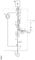
- FIG. 2 is a circuit diagram showing a main part of the uninterruptible power supply 1 shown in FIG. While FIG. 1 shows only a portion related to one phase of the three-phase AC voltage, FIG. 2 shows a portion related to three phases. Also, illustration of the electromagnetic contactors 2 and 14, the semiconductor switch 15, the operation unit 17, and the control device 18 is omitted.
- the uninterruptible power supply 1 includes AC input terminals T1a, T1b, T1c, AC output terminals T2a, T2b, T2c, current detectors 3, 11, capacitors 4a, 4b, 4c, 13a, 13b, 13c, and a reactor. 5a, 5b, 5c, 12a, 12b, and 12c, a converter 6, DC lines L1 and L2, and an inverter 10 are provided.
- the AC input terminals T1a, T1b, T1c receive three-phase AC voltages (U-phase AC voltage, V-phase AC voltage, and W-phase AC voltage) from the commercial AC power supply 21 (FIG. 1), respectively.
- a three-phase AC voltage synchronized with the three-phase AC voltage from the commercial AC power supply 21 is output to the AC output terminals T2a, T2b, and T2c.
- the load 22 is driven by a three-phase AC voltage from the AC output terminals T2a, T2b, T2c.
- One terminal of each of reactors 5a, 5b, 5c is connected to AC input terminals T1a, T1b, T1c, respectively, and the other terminal thereof is connected to input nodes 6a, 6b, 6c of converter 6, respectively.
- One electrodes of capacitors 4a, 4b, 4c are connected to one terminals of reactors 5a to 5c, respectively, and the other electrodes are connected to neutral point NP.
- Capacitors 4a to 4c and reactors 5a to 5c form a low-pass filter, which allows commercial frequency three-phase AC power to pass from AC input terminals T1a, T1b, and T1c to converter 6, and controls the switching frequency generated by converter 6. Cut off the signal.
- the instantaneous value of the AC input voltage Vin appearing at one terminal of the reactor 5a is detected by the control device 18 (FIG. 1).
- the current detector 3 detects an AC input current Iin flowing through the node N1 (that is, the AC input terminal T1a), and supplies a signal Iin indicating the detected value to the control device 18.
- the converter 6 includes IGBTs (Insulated Gate Bipolar Transistors) Q1 to Q6 and diodes D1 to D6.
- the IGBT constitutes a “switching element”.
- the collectors of IGBTs Q1-Q3 are all connected to DC line L1, and their emitters are connected to input nodes 6a, 6b, 6c, respectively.
- the collectors of IGBTs Q4 to Q6 are connected to input nodes 6a, 6b, 6c, respectively, and their emitters are all connected to DC line L2.
- Diodes D1 to D6 are connected in anti-parallel to IGBTs Q1 to Q6, respectively.
- IGBTs Q1 and Q4 are controlled by gate signals Au and Bu, respectively
- IGBTs Q2 and Q5 are controlled by gate signals Av and Bv, respectively
- IGBTs Q3 and Q6 are controlled by gate signals Aw and Bw, respectively.
- the gate signals Bu, Bv, Bw are inverted signals of the gate signals Au, Av, Aw, respectively.
- the IGBTs Q1 to Q3 are turned on when the gate signals Au, Av, Aw are set to the "H (logic high)” level, and the gate signals Au, Av, Aw are set to the "L (logic low)” level, respectively. If you want to turn off.
- the IGBTs Q4 to Q6 are turned on when the gate signals Bu, Bv, Bw are set to “H” level, and are turned off when the gate signals Bu, Bv, Bw are set to “L” level.
- Each of the gate signals Au, Bu, Av, Bv, Aw, and Bw is a pulse signal train, and is a PWM (Pulse Width Modulation) signal.
- the phases of the gate signals Au and Bu, the phases of the gate signals Av and Bv, and the phases of the gate signals Aw and Bw are shifted by 120 degrees.
- the gate signals Au, Bu, Av, Bv, Aw, Bw are generated by the control device 18.
- the IGBTs Q1 and Q5 are turned on, and the reactor 5a, the IGBT Q1, the DC line L1, the capacitor 9, and the DC line L2 are turned on from the AC input terminal T1a.
- IGBT Q5, and reactor 5b a current flows to AC input terminal T1b, and capacitor 9 is charged to a positive voltage.
- Each of the IGBTs Q1 to Q6 is turned on and off at a predetermined timing by the gate signals Au, Bu, Av, Bv, Aw, and Bw, and by adjusting the on time of each of the IGBTs Q1 to Q6, the input nodes 6a to 6c are connected to the input nodes 6a to 6c. It is possible to convert the given three-phase AC voltage into a DC voltage VDC (voltage between terminals of the capacitor 9).
- Inverter 10 includes IGBTs Q11 to Q16 and diodes D11 to D16.
- the IGBT constitutes a “switching element”.
- the collectors of IGBTs Q11 to Q13 are all connected to DC line L1, and their emitters are connected to output nodes 10a, 10b, 10c, respectively.
- the collectors of IGBTs Q14 to Q16 are connected to output nodes 10a, 10b, 10c, respectively, and their emitters are all connected to DC line L2.
- Diodes D11 to D16 are connected in anti-parallel to IGBTs Q11 to Q16, respectively.
- IGBTs Q11 and Q14 are controlled by gate signals Xu and Yu
- IGBTs Q12 and Q15 are controlled by gate signals Xv and Yv, respectively
- IGBTs Q13 and Q16 are controlled by gate signals Xw and Yw, respectively.
- the gate signals Yu, Yv, Yw are inverted signals of the gate signals Xu, Xv, Xw, respectively.
- IGBTs Q11 to Q13 turn on when gate signals Xu, Xv, Xw are set to H level, and turn off when gate signals Xu, Xv, Xw are set to L level, respectively.
- the IGBTs Q14 to Q16 turn on when the gate signals Yu, Yv, Yw are set to H level, and turn off when the gate signals Yu, Yv, Yw are set to L level, respectively.
- Each of the gate signals Xu, Yu, Xv, Yv, Xw, Yw is a pulse signal train and is a PWM signal.
- the phase of the gate signals Xu, Yu, the phase of the gate signals Xv, Yv, and the phase of the gate signals Xw, Yw are shifted by 120 degrees.
- the gate signals Xu, Yu, Xv, Yv, Xw, Yw are generated by the control device 18.
- the positive DC line L1 is connected to the output node 10a via the IGBT Q11, and the output node 10b is connected to the negative DC line L2 via the IGBT Q15.
- 10b output a positive voltage.
- Each of the IGBTs Q11 to Q16 is turned on and off at a predetermined timing by the gate signals Xu, Yu, Xv, Yv, Xw, and Yw, and the on time of each of the IGBTs Q11 to Q16 is adjusted. Can be converted to a three-phase AC voltage.
- Each of reactors 12a-12c is connected to output nodes 10a, 10b, 10c of inverter 10, and the other terminal is connected to each of AC output terminals T2a, T2b, T2c.
- One electrodes of capacitors 13a, 13b, 13c are connected to the other terminals of reactors 12a to 12c, respectively, and the other electrodes are all connected to neutral point NP.
- Reactors 12a to 12c and capacitors 13a, 13b, and 13c constitute a low-pass filter, and pass three-phase AC power of a commercial frequency from inverter 10 to AC output terminals T2a, T2b, and T2c. Cut off frequency signals.
- the current detector 11 detects the inverter output current Iinv flowing through the reactor 12a, and supplies a signal Iinv indicating the detected value to the control device 18.
- the instantaneous value of AC output voltage Vout appearing at the other terminal (node N2) of reactor 12a is detected by control device 18 (FIG. 1).
- FIG. 3 is a diagram for explaining the flow of electric power in the eco mode.
- the semiconductor switch 15 is turned on and the electromagnetic contactor 14 is turned off.
- the three-phase AC power supplied from the commercial AC power supply 21 is supplied to the load 22 via the semiconductor switch 15, as indicated by the black arrow in FIG. That is, power is supplied to load 22 without passing through converter 6 and inverter 10. Therefore, since the occurrence of power loss in converter 6 and inverter 10 is suppressed, the operation efficiency of uninterruptible power supply 1 can be improved.
- the DC power can be stored in the battery 23 by operating the converter 6 and the bidirectional chopper 7 as necessary, as indicated by the white arrow in FIG.
- control device 18 switches the uninterruptible power supply 1 from the inverter power supply mode to the eco mode. Specifically, control device 18 controls on / off of electromagnetic contactor 14 and semiconductor switch 15 so that the power path shown in FIG. 3 is formed. The control device 18 turns on the semiconductor switch 15 and turns off the electromagnetic contactor 14.
- the control device 18 controls the converter 6 and the bidirectional chopper 7 so that the terminal voltage VB of the battery 23 becomes the desired target voltage VBr during the eco mode.
- Converter 6 converts three-phase AC power from commercial AC power supply 21 into DC power and outputs the DC power to DC line L1.
- the bidirectional chopper 7 steps down the DC voltage VDC of the DC line L ⁇ b> 1 and supplies the reduced voltage to the battery 23.
- the controller 18 further detects an instantaneous value of the AC input voltage Vin appearing at the node N1, and detects a voltage drop of the commercial AC power supply 21 based on the detected value. Specifically, control device 18 calculates the degree of voltage drop (unit:%) of commercial AC power supply 21 based on the deviation between the effective value of AC input voltage Vin and the reference voltage.
- the reference voltage is set to, for example, the rated voltage of the commercial AC power supply 21.
- the degree of voltage drop is defined by the deviation of the effective value of the AC input voltage Vin from the reference voltage / the reference voltage.
- control device 18 switches uninterruptible power supply 1 from the eco mode to the inverter power supply mode.
- the threshold is set to, for example, 10%.
- FIG. 4 is a diagram for explaining the flow of power in the inverter power supply mode.
- the control device 18 turns on the electromagnetic contactor 14 and turns off the semiconductor switch 15.
- the control device 18 controls the inverter 10 so as to activate the inverter 10 and convert the DC power supplied from the DC line L1 into three-phase AC power having a commercial frequency.
- the control device 18 further controls the bidirectional chopper 7 so that the terminal voltage VB of the battery 23 is boosted and output to the DC line L1. Thereby, as indicated by the black arrow in FIG. 4, the DC power of the battery 23 is converted into three-phase AC power of the commercial frequency, and supplied to the load 22 via the electromagnetic contactor 14.
- the operation of converter 6 has been stopped.
- Control device 18 stops the operation of inverter 10 when the remaining capacity of battery 23 reaches a predetermined lower limit. Thereby, the uninterruptible power supply 1 ends the inverter power supply.
- the electromagnetic contactor 14 When the voltage drop of the commercial AC power supply 21 is detected in the eco mode in this way, the electromagnetic contactor 14 is turned on, the semiconductor switch 15 is turned off, and the inverter 10 performs the reverse conversion. It is possible to switch from the eco mode to the inverter power supply mode without any interruption.
- the thyristor constituting the thyristor switch is turned off when the current flowing through the thyristor reaches zero when the gate signal is cut off. In other words, the thyristor switch remains on until the current reaches zero even after the gate signal is cut off. Therefore, even if the gate signal of the semiconductor switch 15 is cut off when the voltage drop of the commercial AC power supply 21 is detected, the semiconductor switch 15 is not immediately turned off depending on the timing of cutting off the gate signal, and the node N1 and the node There is a case where the state where N2 is electrically connected via the semiconductor switch 15 continues. When such a case occurs, a current may flow from the node N2 to the node N1 until the semiconductor switch 15 is turned off, as shown in FIG.
- FIG. 5 is a diagram for explaining the flow of electric power when switching from the eco mode to the inverter power supply mode.
- FIG. 5 shows the flow of electric power when switching from the eco mode to the inverter power supply mode after the voltage drop of the commercial AC power supply 21 is detected.
- the DC power of the battery 23 is changed to the three-phase AC power of the commercial frequency as indicated by the black arrow. And supplied to the load 22 via the electromagnetic contactor 14.
- the inverter 10 can control the AC output voltage Vout output to the node N2 to be synchronized with the AC voltage supplied from the commercial AC power supply 21 when the commercial AC power supply 21 is healthy. Thereby, when switching from the eco mode to the inverter power supply mode, it is possible to suppress a momentary drop in the voltage (AC output voltage Vout) output to the AC output terminal T2.
- the semiconductor switch 15 is still in the ON state because the gate signal is cut off but the current is not zero.
- the current flowing through the semiconductor switch 15 is described as “Ists”.
- the direction from node N1 to node N2 is the positive direction of current Ists, and the direction from node N2 to node N1 is the negative direction of current Ists.
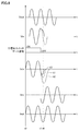
- FIG. 6 is a waveform diagram for explaining the operation of the uninterruptible power supply 1 when switching from the eco mode to the inverter power supply mode.
- FIG. 6 shows waveforms of an AC output voltage Vout, an AC input voltage Vin, a gate signal applied to the semiconductor switch 15, a current Ists flowing through the semiconductor switch 15, an inverter output current Iinv, and a load current Iout.
- one of the pair of thyristors is on according to the polarity of the current Ists.
- one thyristor is in the ON state during the negative half cycle of the current Ists.
- the current Ists becomes 0 after time t1
- one of the thyristors is turned off, and the semiconductor switch 15 is turned off.
- the waveform k1 in FIG. 6 shows a state where the current Ists changes at the same frequency and amplitude as the current Ists before the time t1. In this case, at time t2 when a substantially negative half cycle period has elapsed from time t1, the current Ists becomes zero and the semiconductor switch 15 is turned off.
- converter 6 when a voltage drop of commercial AC power supply 21 is detected during the eco mode, converter 6 is used to convert instantaneous value of AC input voltage Vin to AC output voltage Vout. Is temporarily increased to more than the instantaneous value of. That is, a relationship of Vin ⁇ Vout is temporarily created between the AC input voltage Vin and the AC output voltage Vout. Note that “temporarily” is intended to create the above relationship in a period from the time when the voltage drop of the commercial AC power supply 21 is detected to the time when the semiconductor switch 15 is turned off. This is because the inverter output current Iinv no longer flows into the semiconductor switch 15 after the semiconductor switch 15 is turned off.
- FIG. 7 is a diagram for explaining the operation of the uninterruptible power supply 1 when switching from the eco mode to the inverter power supply mode.
- FIG. 7 is a diagram showing a flow of electric power when switching from the eco mode to the inverter power supply mode, and is a diagram compared with FIG.
- the control device 18 When a voltage drop of the commercial AC power supply 21 is detected during the eco mode, the control device 18 turns on the electromagnetic contactor 14 and activates the inverter 10 and the bidirectional chopper 7. Thus, as indicated by the black arrow, the DC power of the battery 23 is converted into three-phase AC power of the commercial frequency, and supplied to the load 22 via the electromagnetic contactor 14. On the other hand, although the gate signal is cut off, the semiconductor switch 15 is still in the ON state because the current Ists has not become zero.
- the control device 18 controls the converter 6 to convert (reversely convert) DC power supplied from the bidirectional chopper 7 via the DC line L1 to three-phase AC power.
- the AC output voltage of the converter 6 can be controlled to a desired value.
- the DC power of battery 23 is converted into three-phase AC power by converter 6 and supplied to node N1.
- the control device 18 controls the inverse conversion in the converter 6 so that the instantaneous value of the AC input voltage Vin appearing at the node N1 is equal to or greater than the instantaneous value of the AC output voltage Vout.
- the drop of the AC input voltage Vin can be delayed.
- Vin ⁇ Vout it is possible to suppress the current Ists from flowing from the node N2 toward the node N1 even when the semiconductor switch 15 is in the ON state.
- the inverter output current Iinv can be supplied to the load 22 as the load current Iout as it is, so that the power shortage of the load 22 can be avoided.
- FIG. 8 is a waveform diagram for explaining the operation of the uninterruptible power supply device 1 when switching from the eco mode to the inverter power supply mode, and is a diagram compared with FIG. FIG. 8 shows waveforms of the AC output voltage Vout, the AC input voltage Vin, the gate signal applied to the semiconductor switch 15, the current Ists flowing through the semiconductor switch 15, the inverter output current Iinv, and the load current Iout.
- control device 18 turns on the electromagnetic contactor 14 and cuts off the gate signal of the semiconductor switch 15.
- Control device 18 further activates inverter 10.
- Inverter 10 converts DC power stored in battery 23 into three-phase AC power at a commercial frequency.
- the AC output voltage Vout synchronized with the AC voltage (AC input voltage Vin) supplied from the commercial AC power supply 21 before the occurrence of the voltage drop is output to the node N2. Therefore, the AC output voltage Vout can be maintained even after time t1.
- one of the pair of thyristors is on according to the polarity of the current Ists.
- the current Ists becomes 0 after time t1
- one of the thyristors is turned off, and the entire semiconductor switch 15 is turned off.
- Waveforms k1 and k2 in FIG. 8 are the same as waveforms k1 and k2 shown in FIG. 6, respectively.
- a part of the inverter output current Iinv flows into the semiconductor switch 15, so that the negative current Ists increases.
- control device 18 performs inverse conversion in converter 6 such that a relationship of Vin> Vout is created between the instantaneous value of AC input voltage Vin and the instantaneous value of AC output voltage Vout. Control. As a result, the voltage level of the node N1 becomes higher than that of the node N2, so that the inverter output current Iinv is suppressed from flowing into the semiconductor switch 15, and as a result, is output from the AC output terminal T2 as the load current Iout.
- the current in the opposite direction (positive direction) to the current in the negative direction Ists increases, so that the current Ists can be reduced.
- the current Ists can be made earlier to become zero as compared with the waveform k1. Therefore, the time difference from the time when the gate signal of the semiconductor switch 15 is cut off (time t1) to the time when the current Ists becomes zero can be reduced. As a result, the semiconductor switch 15 can be quickly turned off after the voltage drop of the commercial AC power supply 21 occurs.
- the inverse conversion in the converter 6 only needs to be performed temporarily during a period from when the gate signal of the semiconductor switch 15 is cut off to when the semiconductor switch 15 is turned off.
- the time for performing the reverse conversion in converter 6 is set in advance, and control device 18 operates converter 6 for the predetermined time when the voltage drop of commercial AC power supply 21 is detected. I do.
- the predetermined time can be set to, for example, a length equal to or less than a half cycle of the AC voltage supplied from the commercial AC power supply 21.
- the predetermined time is set to a half cycle of the AC voltage. That at least a half cycle period is required from when the gate signal is cut off until the current Ists of the thyristor of the semiconductor switch 15 becomes 0. That's why.
- the predetermined time is set to a length of not less than 1 / cycle and not more than ⁇ cycle of the AC voltage supplied from commercial AC power supply 21.
- the AC input voltage Vin and the AC output voltage Vout can be ideally synchronized even after the time t1. Therefore, in the example of FIG. 8, the current Ists becomes zero at a time when a substantially negative half cycle period has elapsed from the time t1 as in the waveform k1, and the semiconductor switch 15 is turned off.
- FIG. 9 is a block diagram for describing a control configuration of uninterruptible power supply 1 by control device 18.
- the function of each block shown in FIG. 9 can be realized by at least one of software processing and hardware processing by control device 18.
- control device 18 includes a voltage drop detection unit 30, a converter control unit 32, a chopper control unit 34, an inverter control unit 36, and a switch control unit 38.
- the voltage drop detection unit 30 detects an instantaneous value of the AC input voltage Vin that appears at the node N1, and detects a voltage drop of the commercial AC power supply 21 based on the detected value.
- the voltage drop detection unit 30 calculates the degree of voltage drop of the commercial AC power supply 21 based on the deviation between the effective value of the AC input voltage Vin and the reference voltage (rated voltage).
- the voltage drop detection unit 30 compares the voltage drop degree with a threshold value (for example, 10%).
- a threshold value for example, 10%
- the converter control unit 32 controls the converter 6 based on the signal from the operation unit 17, the AC input voltage Vin, the AC output voltage Vout, and the DC voltage VDC. Specifically, converter control unit 32 controls the forward conversion in converter 6 so that DC voltage VDC becomes a predetermined reference voltage VDCr during the inverter power supply mode. However, if the detection signal DT is received from the voltage drop detection unit 30 during the inverter power supply mode (for example, during a power failure of the commercial AC power supply 21), the converter control unit 32 stops the operation of the converter 6.
- converter control unit 32 stops operation of converter 6.
- the DC power can be stored in the battery 23 by operating the converter 6 as necessary.
- Converter control unit 32 further controls such that, when receiving detection signal DT from voltage drop detection unit 30 during the eco mode, AC input voltage Vin equal to or higher than AC output voltage Vout is output from converter 6 to node N1. , The inverse conversion in the converter 6 is controlled.
- Converter control unit 32 controls the inverse conversion in converter 6 for a predetermined time after receiving detection signal DT, and thereafter stops the operation of converter 6.
- the chopper control unit 34 controls the bidirectional chopper 7 based on a signal from the operation unit 17, the DC voltage VDC, and the terminal voltage VB of the battery 23. Specifically, during the inverter power supply mode, the chopper control unit 34 controls the step-down operation of the bidirectional chopper 7 so that the inter-terminal voltage VB of the battery 23 becomes the target voltage VBr. When receiving the detection signal DT from the voltage drop detection unit 30 during the inverter power supply mode, the chopper control unit 34 controls the boosting operation in the bidirectional chopper 7 so that the DC voltage VDC becomes the reference voltage VDCr.
- the chopper control unit 34 stops the operation of the bidirectional chopper 7.
- the DC power can be stored in the battery 23 by operating the bidirectional chopper 7 together with the operation of the converter 6.
- the chopper control unit 34 controls the boosting operation in the bidirectional chopper 7 so that the DC voltage VDC becomes the reference voltage VDCr.
- the inverter control unit 36 controls the inverter 10 based on a signal from the operation unit 17, the AC output voltage Vout, and the inverter output current Iinv. Specifically, during the inverter power supply mode, the inverter control unit 36 controls the inverter 10 such that an AC voltage synchronized with the AC voltage supplied from the commercial AC power supply 21 is output from the inverter 10.
- the inverter control unit 36 In contrast, during the eco mode, the inverter control unit 36 generates a gate signal for turning on and off the semiconductor switching element included in the inverter 10. Inverter control unit 36 generates a gate signal so that AC voltage synchronized with AC voltage supplied from commercial AC power supply 21 is output from inverter 10. However, the inverter control unit 36 does not output the generated gate signal to the inverter 10 during the eco mode. Therefore, the inverter 10 is not operated during the eco mode and enters a standby state until a gate signal is input from the inverter control unit 36.
- the inverter control unit 36 activates the inverter 10 in the standby state and outputs the generated gate signal to the inverter 10. As a result, the inverter 10 is activated, and is switched from the eco mode to the inverter power supply mode.
- the switch control unit 38 controls on / off of the electromagnetic contactor 14 and the semiconductor switch 15 based on a signal from the operation unit 17.
- the switch control unit 38 turns on the electromagnetic contactor 14 and turns off the semiconductor switch 15.
- the switch control unit 38 blocks a gate signal applied to a pair of thyristors constituting the semiconductor switch 15. After the interruption of the gate signal, when the current flowing through the thyristor becomes zero, the semiconductor switch 15 is turned off.
- the switch control unit 38 turns on the semiconductor switch 15 and turns off the electromagnetic contactor 14 by applying a gate signal to each thyristor.
- the power path shown in FIG. 2 is formed between the commercial AC power supply 21 and the load 22.
- the switch control unit 38 When receiving the detection signal DT from the voltage drop detection unit 30 during the eco mode, the switch control unit 38 turns on the electromagnetic contactor 14 and turns off the semiconductor switch 15. As described above, the converter control unit 32 controls the reverse conversion in the converter 6 for a predetermined time after the switch control unit 38 cuts off the gate signal of each thyristor of the semiconductor switch 15. As a result, the AC input voltage Vin increases to a voltage level equal to or higher than the AC output voltage Vout, so that it is possible to suppress the inverter output current Iinv from flowing into the node N1 via the semiconductor switch 15.
- FIG. 10 is a flowchart illustrating a control process of the uninterruptible power supply 1 by the control device 18.
- the control device 18 executes the control processing illustrated in FIG. 10, the function of the control device 18 illustrated in FIG. 9 is realized in the uninterruptible power supply 1.
- control device 18 determines in step S01 whether or not uninterruptible power supply 1 is in the eco mode.
- the control device 18 determines that the uninterruptible power supply 1 is in the eco mode. If the uninterruptible power supply 1 is not in the eco mode, the subsequent steps S02 to S015 are skipped.
- control device 18 determines in step S02 whether a voltage drop of the commercial AC power supply 21 has been detected. When the degree of voltage drop of commercial AC power supply 21 has not reached the threshold value, control device 18 determines that a voltage drop of commercial AC power supply 21 has been detected.
- control device 18 continues to execute the eco mode. Specifically, the control device 18 applies a gate signal to the semiconductor switch 15 in step S03, and turns off the electromagnetic contactor 14 in step S04. Control device 18 further stops the operation of inverter 10 in step S05. However, control device 18 generates a gate signal such that an AC voltage synchronized with an AC voltage supplied from commercial AC power supply 21 is output from inverter 10. Control device 18 does not output the generated gate signal to inverter 10, and places inverter 10 in a standby state until a gate signal is input.
- control device 18 compares terminal voltage VB of battery 23 with target voltage VBr. If the voltage VB between terminals of the battery 23 is lower than the target voltage VBr (YES in S06), the control device 18 proceeds to step S07, and the converter 6 sets the voltage VB between terminals of the battery 23 to the target voltage VBr. Controls the forward transformation in. In step S08, control device 18 further controls the step-down operation of bidirectional chopper 7 such that inter-terminal voltage VB of battery 23 becomes target voltage VBr.
- control device 18 switches from the eco mode to the inverter power supply mode. Specifically, the control device 18 turns on the electromagnetic contactor 14 in step S09 and cuts off the gate signal of the semiconductor switch 15 in step S10.
- control device 18 causes inverter 10 to operate in step S11.
- Control device 18 activates standby inverter 10 and outputs the generated gate signal to inverter 10.
- Control device 18 further controls the boosting operation in bidirectional chopper 7 such that DC voltage VDC becomes reference voltage VDCr in step S12.
- control device 18 controls the inverse conversion in converter 6 such that AC input voltage Vin equal to or higher than AC output voltage Vout is output from converter 6 to node N1.
- Control device 18 determines in step S14 whether a predetermined time has elapsed since the voltage drop of commercial AC power supply 21 was detected. If the predetermined time has not elapsed from the voltage drop (NO in S14), control device 18 returns to step S13 and controls the reverse conversion in converter 6. On the other hand, if the predetermined time has elapsed from the voltage drop (YES in S14), control device 18 stops operation of converter 6.
- the gate signal of semiconductor switch 15 is cut off and the converter is switched for a predetermined time. 6 causes the instantaneous value of the AC input voltage Vin to increase to the instantaneous value of the AC output voltage Vout or more.
Abstract
Description
図3は、エコモードにおける電力の流れを説明するための図である。エコモードでは、半導体スイッチ15がオンされ、電磁接触器14がオフされる。これにより、図3において黒色矢印で示されるように、商用交流電源21から供給される三相交流電力は半導体スイッチ15を介して負荷22に供給される。すなわち、コンバータ6およびインバータ10を通さずに負荷22に電力が供給される。したがって、コンバータ6およびインバータ10における電力損失の発生が抑制されるため、無停電電源装置1の運転効率を向上させることができる。 Next, the operation of the
FIG. 3 is a diagram for explaining the flow of electric power in the eco mode. In the eco mode, the
Claims (6)
- 交流電源と負荷との間に接続される無停電電源装置であって、
前記交流電源から供給される交流電力を直流電力に順変換するコンバータと、
前記コンバータが出力する直流電力または電力貯蔵装置が出力する直流電力を交流電力に逆変換するインバータと、
前記インバータと前記負荷との間に接続された第1のスイッチと、
前記交流電源と前記負荷との間に接続された第2のスイッチと、
前記コンバータ、前記インバータ、前記第1のスイッチおよび前記第2のスイッチを制御する制御装置とを備え、
前記無停電電源装置は、前記第1のスイッチをオンさせるとともに前記第2のスイッチをオフさせ、前記インバータが出力する交流電力を前記負荷に供給する第1の給電モードと、前記第1のスイッチをオフさせるとともに前記第2のスイッチをオンさせ、前記交流電源からの交流電力を前記負荷に供給する第2の給電モードとを有し、
前記制御装置は、前記第2の給電モードが実行されている場合において前記交流電源の電圧低下を検出したときには、前記第1の給電モードに切り替えるように構成され、
前記制御装置は、前記交流電源の電圧低下を検出したときから所定期間、前記電力貯蔵装置が出力する直流電力を交流電力に変換するように前記コンバータに逆変換を実行させるとともに、前記コンバータから出力される交流電圧の瞬時値が前記インバータから出力される交流電圧の瞬時値以上となるように、前記コンバータにおける逆変換を制御する、無停電電源装置。 An uninterruptible power supply connected between an AC power supply and a load,
A converter for converting AC power supplied from the AC power supply into DC power,
An inverter that inversely converts DC power output by the converter or DC power output by the power storage device into AC power,
A first switch connected between the inverter and the load;
A second switch connected between the AC power supply and the load;
A control device for controlling the converter, the inverter, the first switch and the second switch,
A first power supply mode for turning on the first switch and turning off the second switch to supply AC power output by the inverter to the load; and And turning on the second switch to supply AC power from the AC power supply to the load.
The control device is configured to switch to the first power supply mode when detecting a voltage drop of the AC power supply while the second power supply mode is being executed,
The control device, for a predetermined period from the time when the voltage drop of the AC power supply is detected, causes the converter to perform inverse conversion so as to convert the DC power output from the power storage device into AC power, and outputs the output from the converter. An uninterruptible power supply device that controls reverse conversion in the converter such that the instantaneous value of the AC voltage to be output is equal to or greater than the instantaneous value of the AC voltage output from the inverter. - 前記制御装置は、前記交流電源の電圧低下を検出したときから前記所定期間、前記コンバータから出力される交流電圧の瞬時値が前記インバータから出力される交流電圧の瞬時値よりも高くなるように、前記コンバータにおける逆変換を制御する、請求項1に記載の無停電電源装置。 The control device, the predetermined period from the detection of the voltage drop of the AC power supply, the instantaneous value of the AC voltage output from the converter is higher than the instantaneous value of the AC voltage output from the inverter, The uninterruptible power supply according to claim 1, wherein the uninterruptible power supply controls the reverse conversion in the converter.
- 前記所定期間は、前記交流電源から供給される交流電圧の1/2周期以下に相当する長さに設定される、請求項1または2に記載の無停電電源装置。 3. The uninterruptible power supply according to claim 1, wherein the predetermined period is set to a length corresponding to a half cycle or less of an AC voltage supplied from the AC power supply. 4.
- 前記所定期間は、前記交流電源から供給される交流電圧の1/4周期以上かつ1/2周期以下に相当する長さに設定される、請求項3に記載の無停電電源装置。 4. The uninterruptible power supply according to claim 3, wherein the predetermined period is set to a length corresponding to not less than 周期 cycle and not more than 周期 cycle of the AC voltage supplied from the AC power supply.
- 前記第2のスイッチは、逆並列に接続された1対のサイリスタを有するサイリスタスイッチである、請求項1から4のいずれか1項に記載の無停電電源装置。 The uninterruptible power supply according to any one of claims 1 to 4, wherein the second switch is a thyristor switch having a pair of thyristors connected in anti-parallel.
- 前記制御装置は、前記交流電源の電圧低下を検出すると、前記第1のスイッチをオンさせるとともに前記サイリスタスイッチのゲート信号を遮断し、かつ、前記所定期間、前記コンバータにおける逆変換を制御する、請求項5に記載の無停電電源装置。 The control device, upon detecting a voltage drop of the AC power supply, turns on the first switch and cuts off a gate signal of the thyristor switch, and controls the reverse conversion in the converter for the predetermined period. Item 6. The uninterruptible power supply according to item 5.
Priority Applications (5)
| Application Number | Priority Date | Filing Date | Title |
|---|---|---|---|
| KR1020207012352A KR102376604B1 (en) | 2018-07-23 | 2018-07-23 | uninterruptible power supply |
| PCT/JP2018/027469 WO2020021591A1 (en) | 2018-07-23 | 2018-07-23 | Uninterruptible power supply device |
| US16/650,934 US11075540B2 (en) | 2018-07-23 | 2018-07-23 | Uninterruptible power supply device |
| CN201880070276.3A CN111279576B (en) | 2018-07-23 | 2018-07-23 | Uninterruptible power supply device |
| JP2019529660A JP6957621B2 (en) | 2018-07-23 | 2018-07-23 | Uninterruptible power system |
Applications Claiming Priority (1)
| Application Number | Priority Date | Filing Date | Title |
|---|---|---|---|
| PCT/JP2018/027469 WO2020021591A1 (en) | 2018-07-23 | 2018-07-23 | Uninterruptible power supply device |
Publications (1)
| Publication Number | Publication Date |
|---|---|
| WO2020021591A1 true WO2020021591A1 (en) | 2020-01-30 |
Family
ID=69180923
Family Applications (1)
| Application Number | Title | Priority Date | Filing Date |
|---|---|---|---|
| PCT/JP2018/027469 WO2020021591A1 (en) | 2018-07-23 | 2018-07-23 | Uninterruptible power supply device |
Country Status (5)
| Country | Link |
|---|---|
| US (1) | US11075540B2 (en) |
| JP (1) | JP6957621B2 (en) |
| KR (1) | KR102376604B1 (en) |
| CN (1) | CN111279576B (en) |
| WO (1) | WO2020021591A1 (en) |
Cited By (3)
| Publication number | Priority date | Publication date | Assignee | Title |
|---|---|---|---|---|
| WO2022003844A1 (en) * | 2020-06-30 | 2022-01-06 | Toa株式会社 | Public address system |
| WO2022054131A1 (en) * | 2020-09-08 | 2022-03-17 | 東芝三菱電機産業システム株式会社 | Uninterruptible power supply device |
| JP7326614B1 (en) | 2021-12-22 | 2023-08-15 | 東芝三菱電機産業システム株式会社 | Uninterruptible power system and how to update an uninterruptible power system |
Families Citing this family (7)
| Publication number | Priority date | Publication date | Assignee | Title |
|---|---|---|---|---|
| US11063450B2 (en) * | 2018-08-31 | 2021-07-13 | S&C Electric Company | System and method for closed-transition transfer of DC battery banks on a grid scale battery energy storage system |
| EP3672054B1 (en) * | 2018-12-21 | 2021-06-16 | Eltek AS | Power converter and method of controlling a power converter |
| JP6816307B1 (en) * | 2019-06-17 | 2021-01-20 | 東芝三菱電機産業システム株式会社 | Abnormality detection method for power supply and AC power supply |
| US11387670B2 (en) * | 2020-01-31 | 2022-07-12 | Schneider Electric It Corporation | Double conversion on line ups with pass through neutral employing single DC bus |
| CN112366805B (en) * | 2020-10-12 | 2023-05-02 | 深圳供电局有限公司 | Uninterruptible power supply parallel control equipment, uninterruptible power supply parallel control method and inverter power supply system |
| CN112737095A (en) * | 2021-01-29 | 2021-04-30 | 武汉船用电力推进装置研究所(中国船舶重工集团公司第七一二研究所) | Inverter power supply and uninterrupted power supply automatic switching method |
| US11888344B2 (en) * | 2022-04-26 | 2024-01-30 | Schneider Electric It Corporation | Reversed power and grid support with a modular approach |
Citations (2)
| Publication number | Priority date | Publication date | Assignee | Title |
|---|---|---|---|---|
| WO2015198447A1 (en) * | 2014-06-26 | 2015-12-30 | 東芝三菱電機産業システム株式会社 | Uninterruptible power supply |
| JP2017112769A (en) * | 2015-12-17 | 2017-06-22 | 京セラドキュメントソリューションズ株式会社 | Backup power supply device and image forming apparatus provided with the same |
Family Cites Families (10)
| Publication number | Priority date | Publication date | Assignee | Title |
|---|---|---|---|---|
| JP2005229664A (en) * | 2004-02-10 | 2005-08-25 | Fuji Electric Systems Co Ltd | Uninterruptible power supply |
| US7372177B2 (en) | 2005-01-27 | 2008-05-13 | General Electric Company | Control system, method and product for uninterruptible power supply |
| JP4759535B2 (en) * | 2007-06-14 | 2011-08-31 | 三菱電機株式会社 | Uninterruptible power system |
| JP5882884B2 (en) * | 2012-12-20 | 2016-03-09 | 東芝三菱電機産業システム株式会社 | Uninterruptible power system |
| US10958184B2 (en) * | 2014-07-09 | 2021-03-23 | Abb Schweiz Ag | Uninterruptible power supply and method of operation |
| EP3232532A4 (en) * | 2014-12-08 | 2018-08-15 | Toshiba Mitsubishi-Electric Industrial Systems Corporation | Uninterruptible power supply device |
| KR20180011219A (en) * | 2015-06-02 | 2018-01-31 | 도시바 미쓰비시덴키 산교시스템 가부시키가이샤 | Uninterruptible power supply |
| CN109075605B (en) * | 2016-04-27 | 2021-09-03 | 东芝三菱电机产业系统株式会社 | Uninterruptible power supply device |
| CN109952690A (en) * | 2016-11-11 | 2019-06-28 | 东芝三菱电机产业系统株式会社 | Uninterrupted power supply |
| WO2018163397A1 (en) * | 2017-03-10 | 2018-09-13 | 東芝三菱電機産業システム株式会社 | Uninterruptible power supply unit and uninterruptible power supply unit test method |
-
2018
- 2018-07-23 WO PCT/JP2018/027469 patent/WO2020021591A1/en active Application Filing
- 2018-07-23 CN CN201880070276.3A patent/CN111279576B/en active Active
- 2018-07-23 KR KR1020207012352A patent/KR102376604B1/en active IP Right Grant
- 2018-07-23 JP JP2019529660A patent/JP6957621B2/en active Active
- 2018-07-23 US US16/650,934 patent/US11075540B2/en active Active
Patent Citations (2)
| Publication number | Priority date | Publication date | Assignee | Title |
|---|---|---|---|---|
| WO2015198447A1 (en) * | 2014-06-26 | 2015-12-30 | 東芝三菱電機産業システム株式会社 | Uninterruptible power supply |
| JP2017112769A (en) * | 2015-12-17 | 2017-06-22 | 京セラドキュメントソリューションズ株式会社 | Backup power supply device and image forming apparatus provided with the same |
Cited By (4)
| Publication number | Priority date | Publication date | Assignee | Title |
|---|---|---|---|---|
| WO2022003844A1 (en) * | 2020-06-30 | 2022-01-06 | Toa株式会社 | Public address system |
| WO2022054131A1 (en) * | 2020-09-08 | 2022-03-17 | 東芝三菱電機産業システム株式会社 | Uninterruptible power supply device |
| JP7108130B1 (en) * | 2020-09-08 | 2022-07-27 | 東芝三菱電機産業システム株式会社 | Uninterruptible power system |
| JP7326614B1 (en) | 2021-12-22 | 2023-08-15 | 東芝三菱電機産業システム株式会社 | Uninterruptible power system and how to update an uninterruptible power system |
Also Published As
| Publication number | Publication date |
|---|---|
| KR102376604B1 (en) | 2022-03-18 |
| CN111279576A (en) | 2020-06-12 |
| US11075540B2 (en) | 2021-07-27 |
| CN111279576B (en) | 2023-01-10 |
| KR20200062283A (en) | 2020-06-03 |
| JPWO2020021591A1 (en) | 2020-07-30 |
| JP6957621B2 (en) | 2021-11-02 |
| US20200295595A1 (en) | 2020-09-17 |
Similar Documents
| Publication | Publication Date | Title |
|---|---|---|
| WO2020021591A1 (en) | Uninterruptible power supply device | |
| JP6190059B2 (en) | Uninterruptible power system | |
| JP6203289B2 (en) | Power converter | |
| TWI660566B (en) | Power converter | |
| JP6714157B2 (en) | Power supply device and power supply system using the same | |
| WO2017183147A1 (en) | Uninterruptible power supply device | |
| JP6668556B2 (en) | Power supply device and power supply system using the same | |
| US11196292B2 (en) | Uninterruptible power supply system | |
| JP6718019B2 (en) | Power supply | |
| JP3658238B2 (en) | Neutral point clamp type power converter | |
| US11831249B2 (en) | Power conversion apparatus | |
| US20240120769A1 (en) | Uninterruptible power supply apparatus | |
| JP7027576B1 (en) | Uninterruptible power supply system | |
| WO2022137291A1 (en) | End of life determination device and power supply device equipped with same | |
| JPS63206165A (en) | Uninterruptible power supply | |
| JP2017028791A (en) | Power conversion device | |
| JPWO2018185811A1 (en) | Power converter |
Legal Events
| Date | Code | Title | Description |
|---|---|---|---|
| ENP | Entry into the national phase |
Ref document number: 2019529660 Country of ref document: JP Kind code of ref document: A |
|
| 121 | Ep: the epo has been informed by wipo that ep was designated in this application |
Ref document number: 18927749 Country of ref document: EP Kind code of ref document: A1 |
|
| ENP | Entry into the national phase |
Ref document number: 20207012352 Country of ref document: KR Kind code of ref document: A |
|
| NENP | Non-entry into the national phase |
Ref country code: DE |
|
| 122 | Ep: pct application non-entry in european phase |
Ref document number: 18927749 Country of ref document: EP Kind code of ref document: A1 |