WO2020009152A1 - 微小電極、及びその製造方法、並びに集積デバイス - Google Patents
微小電極、及びその製造方法、並びに集積デバイス Download PDFInfo
- Publication number
- WO2020009152A1 WO2020009152A1 PCT/JP2019/026472 JP2019026472W WO2020009152A1 WO 2020009152 A1 WO2020009152 A1 WO 2020009152A1 JP 2019026472 W JP2019026472 W JP 2019026472W WO 2020009152 A1 WO2020009152 A1 WO 2020009152A1
- Authority
- WO
- WIPO (PCT)
- Prior art keywords
- layer
- microelectrode
- polymer compound
- thickness
- conductive layer
- Prior art date
- Legal status (The legal status is an assumption and is not a legal conclusion. Google has not performed a legal analysis and makes no representation as to the accuracy of the status listed.)
- Ceased
Links
Images




Classifications
-
- G—PHYSICS
- G01—MEASURING; TESTING
- G01N—INVESTIGATING OR ANALYSING MATERIALS BY DETERMINING THEIR CHEMICAL OR PHYSICAL PROPERTIES
- G01N27/00—Investigating or analysing materials by the use of electric, electrochemical, or magnetic means
- G01N27/26—Investigating or analysing materials by the use of electric, electrochemical, or magnetic means by investigating electrochemical variables; by using electrolysis or electrophoresis
- G01N27/28—Electrolytic cell components
- G01N27/30—Electrodes, e.g. test electrodes; Half-cells
- G01N27/327—Biochemical electrodes, e.g. electrical or mechanical details for in vitro measurements
-
- A—HUMAN NECESSITIES
- A61—MEDICAL OR VETERINARY SCIENCE; HYGIENE
- A61B—DIAGNOSIS; SURGERY; IDENTIFICATION
- A61B5/00—Measuring for diagnostic purposes; Identification of persons
- A61B5/05—Detecting, measuring or recording for diagnosis by means of electric currents or magnetic fields; Measuring using microwaves or radio waves
- A61B5/053—Measuring electrical impedance or conductance of a portion of the body
- A61B5/0538—Measuring electrical impedance or conductance of a portion of the body invasively, e.g. using a catheter
-
- A—HUMAN NECESSITIES
- A61—MEDICAL OR VETERINARY SCIENCE; HYGIENE
- A61B—DIAGNOSIS; SURGERY; IDENTIFICATION
- A61B5/00—Measuring for diagnostic purposes; Identification of persons
- A61B5/24—Detecting, measuring or recording bioelectric or biomagnetic signals of the body or parts thereof
- A61B5/25—Bioelectric electrodes therefor
- A61B5/263—Bioelectric electrodes therefor characterised by the electrode materials
-
- G—PHYSICS
- G01—MEASURING; TESTING
- G01N—INVESTIGATING OR ANALYSING MATERIALS BY DETERMINING THEIR CHEMICAL OR PHYSICAL PROPERTIES
- G01N27/00—Investigating or analysing materials by the use of electric, electrochemical, or magnetic means
- G01N27/26—Investigating or analysing materials by the use of electric, electrochemical, or magnetic means by investigating electrochemical variables; by using electrolysis or electrophoresis
- G01N27/28—Electrolytic cell components
- G01N27/30—Electrodes, e.g. test electrodes; Half-cells
- G01N27/305—Electrodes, e.g. test electrodes; Half-cells optically transparent or photoresponsive electrodes
-
- A—HUMAN NECESSITIES
- A61—MEDICAL OR VETERINARY SCIENCE; HYGIENE
- A61B—DIAGNOSIS; SURGERY; IDENTIFICATION
- A61B2562/00—Details of sensors; Constructional details of sensor housings or probes; Accessories for sensors
- A61B2562/02—Details of sensors specially adapted for in-vivo measurements
- A61B2562/0209—Special features of electrodes classified in A61B5/24, A61B5/25, A61B5/283, A61B5/291, A61B5/296, A61B5/053
Definitions
- the present invention relates to a microelectrode, a method for manufacturing the microelectrode, and an integrated device.
- Non-Patent Document 1 Conventionally, after transferring graphene to a flexible polymer substrate, the buckling is artificially applied to measure the optical and electrical characteristics (Non-Patent Document 1). However, it is difficult to produce a fine three-dimensional shape on a micrometer scale by the method of adding buckling. Therefore, attention has been paid to a method of transferring graphene onto a thin film element that can be assembled into a small three-dimensional shape in a self-organized manner, and using the thin film element as a power source to produce fine three-dimensional graphene (non- Patent Document 2).
- Non-Patent Document 3 an electrode element manufactured by transferring graphene to polyparaxylene (parylene), which is a polymer material having many aromatic rings, is also disclosed (Non-Patent Document 3).
- an electric signal of a living tissue is stably measured while the structure is maintained by embedding an electrode element in a living body.
- T.M.G.Mohiuddin Uniaxial strain in graphene by Raman spectroscopy: G peak splitting, Gruneisen parameters, and sample orientation.
- Phys. T.Deng et.al., Self-folding graphene-polymer bilayers. Appl.Phys.Lett., 2015,106,203108-1-4.
- D.W.Park et.al., phenGraphene-based carbon-layered electrode array technology for neural imaging and optogenetic5applications. Nat.Comm., 2014,5,5258-1-22.
- Non-Patent Document 2 has a technical problem that, due to low adhesion between graphene and a thin film element, graphene is separated from the surface, slips off, and is broken due to partial stress concentration. .
- peeling or side slippage is unlikely to occur because parylene having high adhesion to graphene is used, but the degree of freedom in design according to the application is low because of the two-dimensional planar structure. There is a problem.
- an object of the present invention is to provide a microelectrode having an arbitrary three-dimensional curved shape in which peeling, skidding, disconnection, and the like are suppressed, a manufacturing method thereof, and an integrated device including the microelectrode.
- One embodiment of the present invention is a microelectrode having a stacked structure, which includes a layer containing a polymer compound having an aromatic ring (a polymer compound layer) and a layer containing a conductive material (a conductive layer).
- One embodiment of the present invention is the above microelectrode, wherein the conductive material is a conductive carbon material.
- the polymer compound layer includes polyparaxylene or a derivative thereof.
- One embodiment of the present invention is the above microelectrode, wherein the polymer compound layer and the conductive layer are arranged adjacent to each other.
- One embodiment of the present invention is a method for manufacturing a microelectrode having a three-dimensional curved shape, comprising: (a) a layer containing a polymer compound having an aromatic ring having a thickness of 10 to 900 nm (polymer compound layer); A step of forming a laminate including a layer (conductive layer) containing a conductive material having a thickness of 0.3 to 10 nm, and (b) forming the laminate by using a gradient of strain in a thickness direction of the laminate as a driving force. Forming a three-dimensionally curved shape on the body in a self-organizing manner.
- One embodiment of the present invention is the above-described method for manufacturing a microelectrode, wherein after the step (a) and before the step (b), (c) forming a part or all of the layers of the laminate, The method further includes a step of patterning into an arbitrary shape.
- One embodiment of the present invention is an integrated device including the microelectrode.
- a microelectrode having an arbitrary three-dimensional curved shape in which peeling, skidding, disconnection, and the like are suppressed, a manufacturing method thereof, and an integrated device including the microelectrode.
- FIG. 3 is a perspective view of a microelectrode according to one embodiment of the present invention.
- FIG. 4 is a schematic view of a method for manufacturing a microelectrode according to one embodiment of the present invention.
- FIG. 4 is an example of a process diagram for forming a laminated body 20.
- 9 is a phase contrast microscope image showing a state of self-assembly of a rectangular laminate into a cylindrical three-dimensional curved shape after the addition of an EDTA solution. 4 shows the relationship between the radius of curvature of a cylindrical microelectrode which is one embodiment of the present invention and the thickness of each layer of a stack.
- (1) shows the correlation between the radius of curvature of the cylindrical microelectrode and the thickness of the parylene layer (polymer compound layer).
- (2) shows the correlation between the radius of curvature of the cylindrical microelectrode and the number of transferred graphene layers (conductive layers).
- 4 shows changes in Raman spectrum before and after self-assembly of a cylindrical microelectrode which is one embodiment of the present invention.
- Raman spectra of the G band (1) and the 2D band (2) of the two-dimensional planar graphene layer are shown as Before @ folding.
- the Raman spectra of the G band (1) and the 2D band (2) of the three-dimensional microelectrode composed of the two layers of the parylene layer and the graphene layer are shown as After @ folding.
- FIG. 7 shows changes in electrical characteristics of a cylindrical microelectrode according to one embodiment of the present invention before and after self-assembly.
- (1) to (4) show a manufacturing process of a cylindrical microelectrode which is one embodiment of the present invention.
- (5) shows an IV curve of the cylindrical microelectrode before self-assembly (in a dry state, in water) and after self-assembly (after adding the EDTA solution and replacing with pure water).
- 3 shows microelectrodes having various three-dimensional curved shapes.
- (1) shows a microelectrode having a spherical gripper structure.
- (2) shows a cylindrical microelectrode having a pattern in which hexagons are arranged adjacently.
- (3) shows a coil-shaped microelectrode.
- the state of control of the bending direction by the crystal direction of graphene is shown.
- (1) shows a single crystal graphene manufactured in a millimeter size.
- (2) shows a state of bending when a laminate including the parylene layer and the single crystal graphene layer transferred to the parylene layer is peeled off from the substrate.
- (3) shows a conceptual diagram of bending of a stacked body having a single crystal graphene layer.
- the microelectrode according to one embodiment of the present invention is a microelectrode having a stacked structure, which includes a layer containing a polymer compound having an aromatic ring (polymer compound layer) and a layer containing a conductive material (conductive layer).
- the polymer compound layer has a thickness of 10 to 900 nm
- the conductive layer has a thickness of 0.3 to 10 nm, and has a three-dimensional curved shape.
- FIG. 1 illustrates a microelectrode according to one embodiment of the present invention.
- reference numeral 100 denotes a microelectrode
- 11 denotes a conductive layer
- 12 denotes a polymer compound layer.
- the microelectrode 100 has a structure in which a polymer layer 12 is laminated on a conductive layer 11. That is, the conductive layer 11 is disposed outside and the polymer compound layer 12 is disposed inside.
- the conductive layer 11 and the polymer compound layer 12 are arranged adjacent to each other.
- the conductive layer 11 and the polymer compound layer 12 do not necessarily need to be adjacent to each other, but at least a portion forming a three-dimensional curved shape has the conductive layer 11 and the polymer compound layer 12.
- the microelectrode of this embodiment has a three-dimensional curved shape.
- “having a three-dimensionally curved shape” means that at least a part of the structure of the microelectrode has a three-dimensionally curved shape.
- the entire structure of the microelectrode 100 has a cylindrically curved shape.
- the cylindrical microelectrode as shown in FIG. 1 is a preferred example of the microelectrode of the present embodiment.
- the three-dimensional curved shape that the microelectrode of this embodiment may have is not limited to the example of FIG. 1, and for example, a part of the structure may have a three-dimensionally curved shape (for example, , FIG. 7 (4)).
- it may have a spherical gripper structure or a spiral structure (for example, see FIG. 8).
- various three-dimensional curved shapes such as a biological tissue-like structure can be used. By changing the thickness and shape of the conductive layer and the polymer compound layer in the microelectrode of this embodiment, those having various three-dimensional curved shapes can be designed.
- the conductive layer 11 is a layer containing a conductive material.
- the conductive material used for the conductive layer 11 is not particularly limited as long as it has conductivity, but is preferably a nanomaterial (a material having at least one dimension of 100 nm or less) that can be processed into a thin film shape. Further, a material that does not induce a large change in volume when immersed in a solution is preferable.
- the conductive material is preferably a biocompatible material. Further, the conductive material is preferably a substance that has ⁇ - ⁇ interaction with the polymer compound contained in the polymer compound layer 12.
- the adhesion between the conductive layer 11 and the polymer compound layer 12 can be increased.
- the conductive material include a conductive carbon material such as graphene and carbon nanotube, and a planar substance such as molybdenum disulfide.
- the conductive material preferably contains a conductive carbon material, and more preferably contains graphene.
- the conductive material contained in the conductive layer 11 may be one kind or two or more kinds, but is preferably one kind.
- the conductive layer 11 may be made of graphene, or may be made of bucky paper obtained by processing carbon nanotubes into a sheet.
- the conductive layer 11 may be composed of a single layer or a plurality of layers of a conductive material.
- the number of conductive materials is not particularly limited, but is, for example, 2 to 30, 2 to 20, 2 to 10, or 2 to 5 layers. Etc. are exemplified.
- the conductive layer 11 is preferably composed of 1 to 30 layers of a conductive carbon material, and more preferably composed of 1 to 4 layers of a conductive carbon material in order to maintain the transparency of the three-dimensional shape. .
- the conductive layer 11 is more preferably composed of 1 to 30 layers of graphene, and particularly preferably composed of 1 to 4 layers of graphene in order to maintain three-dimensional transparency.
- the conductive layer 11 is made of graphene, it may be polycrystalline graphene or single crystal graphene, but from the viewpoint of controlling the direction of the curved shape, single crystal graphene is preferable.
- the thickness of the conductive layer 11 is 0.3 to 10 nm.
- the total thickness of the plurality of layers is the thickness of the conductive layer 11.
- the thickness of the conductive layer 11 is preferably 0.3 to 7 nm, more preferably 0.3 to 5 nm, and 0.3 to 1.2 nm. Is more preferable.
- the microelectrode 100 having an arbitrary three-dimensional curved shape can be obtained.
- the radius of curvature of the three-dimensional curved shape can be reduced.
- the polymer compound layer 12 is a layer containing a polymer compound having an aromatic ring.
- the high molecular compound used for the high molecular compound layer 12 preferably has many aromatic rings in the molecule and has ⁇ - ⁇ interaction with the conductive material included in the conductive layer 11.
- the adhesion of the polymer compound layer 12 to the conductive layer 11 is increased.
- a polymer compound having high transparency and no cytotoxicity examples include polyparaxylene or a derivative thereof.
- polyparaxylene derivatives include polymers of halogenated paraxylene (chloroparaxylene, fluoroparaxylene, etc.). Among them, the polymer compound is more preferably polyparaxylene.
- the polymer compound contained in the polymer compound layer 12 may be one type or two or more types, but is preferably one type.
- the thickness of the polymer compound layer 12 is 10 to 900 nm.
- the total thickness of the plurality of thin films is the thickness of the polymer compound layer 12.
- the microelectrode 100 having an arbitrary three-dimensional curved shape can be obtained.
- the radius of curvature of the three-dimensional curved shape can be increased.
- the ratio of the thickness of the conductive layer 11 to the thickness of the polymer compound layer 12 is not particularly limited as long as it is in the range of 1/3000 to 1/1. More preferably, it is 1200 to 1/4. By setting the thickness ratio between the conductive layer 11 and the polymer compound layer 12 within the above range, a stable three-dimensional curved shape can be formed.
- the microelectrode of this embodiment may have other configurations in addition to the conductive layer 11 and the polymer compound layer 12 as long as the effects of the present invention are not impaired.
- Other configurations include, for example, a metal layer.
- the metal layer is a layer containing a metal element.
- the metal element contained in the metal layer is not particularly limited as long as it is one usually used as a metal electrode, and examples thereof include noble metals such as gold, silver, platinum, palladium, rhodium, iridium, ruthenium, and iridium.
- the thickness of the metal layer is not particularly limited, but is preferably, for example, 10 nm to 100 ⁇ m.
- the metal layer be disposed in a portion that does not have a three-dimensional curved shape.
- the total thickness (the total thickness of the conductive layer 11, the polymer compound layer 12, and optionally the metal layer and the other layers) of the portion having a three-dimensional curved shape is determined by the manufacturing method described later.
- the thickness is preferably about 10 to 500 nm so as not to prevent bending in the process.
- the conductive layer is formed of graphene
- the polymer compound layer is formed of polyparaxylene or a derivative thereof
- the conductive layer and the polymer compound layer are adjacent to each other. Is mentioned.
- a three-dimensional curved shape can be formed by setting the thickness of the polymer compound layer containing the polymer compound having an aromatic ring and the thickness of the conductive layer respectively.
- a high molecular compound having an aromatic ring for the high molecular compound layer, adhesion to the conductive layer is increased, and occurrence of peeling, side slip, disconnection, and the like can be suppressed.
- a microelectrode having a three-dimensional curved shape of any design can be obtained.
- the bending direction can be defined to an arbitrary direction.
- the microelectrode of the present embodiment can be relocated to an arbitrary location by operation with a micromanipulator, and can be used for evaluation of electrical characteristics, integration into a device, assembly of a circuit, and the like.
- graphene when graphene is used as a conductive material and polyparaxylene or a derivative thereof is used as a high molecular compound, since graphene and polyparaxylene or a derivative thereof are both highly robust materials, they are immersed in a liquid for a long time. Even when the liquid is subjected to a change in temperature or a change in the temperature of the liquid, a shape change or distortion hardly occurs.
- graphene and polyparaxylene or their derivatives have high transparency, they do not block the optical path during observation with a microscope, and can be used in all types of microscopes regardless of whether they are upright or inverted. . Furthermore, high-definition observation by observation under a super-resolution microscope can be realized. In addition, handling such as collection and movement can be performed by pipetting, and a plurality of microelectrodes can be structured using a glass capillary. In addition, if a material having high biocompatibility is used as the conductive material and the high molecular compound, application as an electrode interface with cells or tissues is also possible. Graphene and polyparaxylene or a derivative thereof are also suitable as a highly biocompatible material.
- the method for manufacturing a microelectrode having a three-dimensional curved shape includes: (a) a layer containing a polymer compound having an aromatic ring having a thickness of 10 to 900 nm (polymer compound layer); Forming a laminate including a layer (conductive layer) containing a conductive material having a thickness of 0.3 to 10 nm; and (b) applying a gradient of strain in a thickness direction of the laminate as a driving force to the laminate. Forming a three-dimensional curved shape in a self-organizing manner.
- a method for manufacturing a microelectrode of the present invention will be described with reference to the drawings showing a preferred embodiment of the present invention.
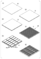
- FIG. 2 is a diagram schematically illustrating a method for manufacturing a microelectrode according to one embodiment of the present invention.
- a laminate 20 including the conductive layer 11 and the polymer compound layer 12 is formed (FIGS. 2A and 2B: step (a)).
- the conductive layer 11 and the polymer compound layer 12 are formed respectively (FIG. 1A), and the conductive layer 11 is transferred to the polymer compound layer 12 ( 1 (2)), a laminate 20 is formed.
- the laminate 20 is formed into a three-dimensional curved shape in a self-organizing manner (FIGS. 1 (3) to (6): step (b)).
- a stress distribution is formed in the thickness direction of the laminated body 20 by bringing the conductive layer 11 and the polymer compound layer 12 into close contact with and joining to each other (FIG. 2 (3)).
- a gradient of strain in the in-plane direction is formed (FIG. 2 (4)).
- the conductive layer 11 and the polymer compound layer 12 bend while being joined to each other (FIG. 2 (5)), and a three-dimensional curved shape is assembled in a self-organizing manner (FIG. 2 (6)).
- Step (a) is a step of forming a laminate including (a) a polymer compound layer having a thickness of 10 to 900 nm and a conductive layer having a thickness of 0.3 to 10 nm.
- FIGS. 3A to 3D are diagrams showing a specific example of a method for forming a laminate 20 including the polymer compound layer 12 and the conductive layer 11.
- FIG. 3 (1) to 3 (4) a sacrificial layer 13 is formed on the substrate 10 (FIG. 3 (1)) (FIG. 3 (2)), and a polymer compound layer 12 (FIG. 3 (2)) is further formed thereon. 3 (3)) and the formation of the conductive layer 11 (FIG. 3 (4)), thereby forming the laminate 20.
- the substrate 10 is used for the convenience of forming the laminate 20, and the material is not particularly limited.
- a material of the substrate 10 a material having high surface flatness is preferable. Further, when observing with a fluorescence microscope or the like while enclosing the cells while holding the microelectrodes manufactured by the method of the present embodiment on a substrate, those that do not hinder the fluorescence intensity observation of the cells with a fluorescence microscope, It is preferable that the absorption band of the wavelength does not overlap with the conductive layer 11 as optical characteristics.
- the material of the substrate 10 include silicon, soda glass, quartz, magnesium oxide, and sapphire.
- the thickness of the substrate 10 is not particularly limited, but is preferably about 50 to 200 ⁇ m. Specific examples of the substrate 10 include, for example, a glass substrate having a thickness of about 100 ⁇ m.
- the sacrifice layer 13 has a role as a temporary adhesive layer for releasing the laminate 20 including the conductive layer 11 and the polymer compound layer 12 from the substrate 10.
- the material constituting the sacrificial layer 13 is not particularly limited as long as it has a property of dissolving in response to an external stimulus such as a chemical substance, a temperature change, and light irradiation.
- EDTA ethylenediaminetetraacetic acid
- the laminate 20 is released from the substrate 10 by dissolving the sacrifice layer 13, and the self-assembly is performed on the laminate 20.
- a three-dimensional curved shape can be formed.
- Chelating agents such as sodium citrate and ethylenediaminetetraacetic acid (EDTA) do not show toxicity to biological samples such as cells. Can be included.
- any material having a property of dissolving in response to an external stimulus can be used without being limited to a kind of synthetic polymer or biopolymer.
- a metal thin film that can be dissolved by an etchant, poly (N-isopropylacrylamide) that can induce a gel-sol transition by a change in temperature, and photoresists that can induce a gel-sol transition by ultraviolet irradiation can be preferably used.
- the thickness of the sacrifice layer 13 is not particularly limited.
- the thickness of the sacrificial layer 13 can be, for example, 20 to 1000 nm from the viewpoint of prompt dissolution.
- the method for forming the sacrificial layer 13 on the substrate 10 is not particularly limited, and a method generally used for forming a thin film can be appropriately selected according to the material of the sacrificial layer 13. Examples of a method for forming the sacrificial layer 13 include chemical vapor deposition (CVD), spin coating, inkjet printing, a vapor deposition method, and an electrospray method.
- the conductive layer 11 and the polymer compound layer 12 are the same as those described in the above “ ⁇ Microelectrode>”. 3 (3) and (4), the polymer compound layer 12 is formed on the sacrificial layer 13 and the conductive layer 11 is formed on the polymer compound layer 12. The reverse is also possible. That is, the conductive layer 11 may be formed on the sacrificial layer 13, and the polymer compound layer 12 may be formed on the conductive layer 11.
- the thickness of the conductive layer 11 formed here is 0.3 to 10 nm, and the thickness of the polymer compound layer 12 is 10 to 900 nm.
- a gradient of strain can be generated in the thickness direction of the laminate 20. If the thickness of the conductive layer 11 is increased within the above range, the radius of curvature of the three-dimensional curved shape formed in step (b) described later can be reduced. on the other hand. If the thickness of the polymer compound layer 12 is increased within the above range, the radius of curvature of the three-dimensional curved shape formed in step (b) described later can be increased.
- the method for forming the polymer compound layer 12 is not particularly limited, and CVD, spin coating, inkjet printing, vapor deposition, electrospray, or the like can be used.
- the polymer compound layer 12 when the polymer compound layer 12 is composed of polyparaxylene or a derivative thereof, the polymer compound layer 12 can be formed by growing a dimer of paraxylene or a derivative thereof by CVD.
- the method for forming the conductive layer 11 is not particularly limited, and a transfer method using a water surface, a chemical vapor deposition method (CVD), spin coating, ink jet printing, a thermal evaporation method, an electrospray method, and the like can be used.
- CVD chemical vapor deposition method
- a graphene single-layer film is formed on the surface of a metal film such as a copper foil by using CVD, and the metal film is dissolved and washed repeatedly on the water surface.
- the conductive layer 11 can be formed by transferring the single-layer graphene film to the surface of the polymer compound layer 12 or the sacrificial layer 13. Further, by repeating the above operation, the conductive layer 11 including a plurality of layers of graphene can be formed.
- the laminate 20 formed in this step may include other components in addition to the conductive layer 11 and the polymer compound layer 12. Other configurations are not particularly limited, and can be appropriately selected depending on the purpose. As another configuration, the laminate 20 may include, for example, other layers other than the conductive layer 11 and the polymer compound layer 12. The thickness and the forming method of the other layers can be appropriately selected according to the material constituting the layer. For example, the laminate 20 can include a metal layer as another layer. When the laminate 20 includes a metal layer, the thickness of the metal layer can be, for example, 10 nm to 100 ⁇ m. The metal layer can be provided adjacent to the conductive layer 11.
- the metal layer may be formed on the conductive layer 11.
- a metal layer may be formed on the polymer compound layer 12, and then the conductive layer 11 may be formed on the metal layer.
- a metal layer is not formed in a portion where a three-dimensional curved shape is formed in a step (b) described later.
- the method for forming the metal layer is not particularly limited, and methods such as vapor deposition, sputtering, and direct application (for example, direct application of a silver paste) can be used.
- the step (b) is a step of causing the laminate to form a three-dimensional curved shape in a self-organizing manner by using the gradient of strain in the thickness direction of the laminate as a driving force.
- the gradient of the strain in the thickness direction of the laminate can be obtained by closely contacting and joining the conductive layer 11 and the polymer compound layer 12 each having a predetermined thickness.
- a gradient of strain occurs in the thickness direction of the laminate 20.
- the laminate 20 can be formed into a three-dimensional curved shape in a self-organizing manner by using the gradient of the strain as a driving force.
- the dissolution of the sacrifice layer 13 can be appropriately performed according to the material of the sacrifice layer 13.
- the sacrificial layer 13 is composed of a calcium alginate gel
- the sacrificial layer 13 is dissolved by adding a chelating agent such as sodium citrate or ethylenediaminetetraacetic acid (EDTA), or an enzyme called alginase. be able to.
- EDTA ethylenediaminetetraacetic acid
- the sacrificial layer 13 is a metal thin film that can be dissolved by an etchant
- the sacrificial layer 13 can be dissolved by the etchant.
- Any photoresist that can be dissolved and can induce a gel-sol transition by ultraviolet irradiation can be dissolved by ultraviolet irradiation.
- the manufacturing method includes a step of forming a sacrificial layer 13 on a substrate 10 and a step of forming a laminate 20 including a polymer compound layer 12 and a conductive layer 11 on the sacrificial layer 13. And a step of dissolving the sacrificial layer 13 and causing the laminate 20 to form a three-dimensional curved shape in a self-organizing manner using the gradient of strain in the thickness direction of the laminate 20 as a driving force. May be.
- the step of forming the laminate 20 may be a step of forming the polymer compound layer 12 on the sacrificial layer 13 and forming the conductive layer 11 on the polymer compound layer 12.
- the manufacturing method according to this embodiment may include other steps in addition to the above steps (a) and (b). Other steps are not particularly limited, but as other steps, for example, after the above-mentioned step (a) and before the above-mentioned step (b), (c) adding a part or all of the layers of the laminate to an arbitrary layer
- the method may further include a step of patterning into a shape.
- the patterning method is not particularly limited.
- a microfabrication technique such as a photolithography method, an electron beam lithography method, or a dry etching method can be applied.
- the pattern shape is not particularly limited, and may be any two-dimensional shape and size.
- a rectangular pattern having a length and width of 400 ⁇ m and 200 ⁇ m respectively is shown, but the shape and size of the pattern are not limited thereto.
- the size of the pattern is preferably larger than 10 ⁇ m. If the pattern shape is rectangular, a cylindrical microelectrode can be obtained. If the pattern is radial, a microelectrode having a spherical gripper structure can be obtained (see FIG. 8A).
- the pattern shape is a two-dimensional pattern in which hexagons are adjacently arrayed, it is possible to obtain a microelectrode of a cylindrical structure having a larger, hollow inside, and high material permeability (FIG. 8 ( 2)). If the pattern shape is a parallelogram two-dimensional pattern structure in which both ends of the rectangular pattern have an inclination, a microelectrode of a coil-shaped structure wound along the inclination can be obtained (FIG. 8 ( 3)). Such a coil structure can flexibly change its structure in the major axis direction, and can be applied as an electrode element having high elasticity that is hardly broken.
- a strain gradient is generated in the thickness direction of the laminate.
- the laminate is self-organized to form a three-dimensional curved shape.
- separation, side slip, disconnection, and the like due to a structural change to a three-dimensional shape can be suppressed.
- designing the shape of the laminate to an arbitrary shape and size, a microelectrode having an arbitrary three-dimensional shape and size can be obtained.
- An integrated device is an integrated device including the microelectrode of the above embodiment. Since the microelectrode of the above embodiment can have a fine and arbitrary shape, an electrode device can be three-dimensionally assembled, integrated, and an integrated device can be manufactured. For example, by operating and placing the microelectrode of the above embodiment with a manipulator or the like, tissue structuring and circuit formation can be performed. By using a material having high biocompatibility for the microelectrode, the integrated device of this embodiment can be applied as an electrode interface with cells or tissues, for example.
- Example 1 Production Example of Laminate A microelectrode having a three-dimensional curved shape was produced according to the processes shown in FIGS.
- a glass substrate was used as the substrate 10 shown in FIG.
- a sodium alginate solution was spin-coated, and then immersed in a 100 mM calcium chloride solution to form a sacrificial layer 13 of calcium alginate gel (FIG. 3 (2)).
- the thickness of the sacrificial layer 13 can be controlled by changing the concentration of the sodium alginate solution and the speed of spin coating.
- a 40 nm gel layer was formed by spin coating a 2 wt% sodium alginate solution at 3000 rpm.
- a paraxylene dimer was grown by CVD to form the polymer compound layer 12 made of polyparaxylene (parylene) (FIG. 3 (3)).
- the thickness of the polymer compound layer 12 can be controlled by the weight of the para-xylene dimer used as a raw material for CVD growth.
- a 50-nm polymer compound layer 12 was formed by growing 50 mg of para-xylene dimer on the substrate 10 using a CVD method.
- the conductive layer 11 was transferred to the surface of the polymer compound layer 12.
- the conductive layer 11 a single-layer graphene formed on a surface of a copper foil by using CVD is used.
- the copper foil was dissolved in the ferric chloride solution, and after repeating washing on the water surface, the graphene monolayer (conductive layer 11) was transferred to the surface of the polymer compound layer 12 (FIG. 3 (4)). By repeating this operation, a plurality of layers of graphene can be stacked on the surface of the polymer compound layer 12.
- a photoresist was spin-coated on the conductive layer 11 and irradiated with ultraviolet light through a photomask of an arbitrary shape to form a resist layer 15 (FIG. 3 (5)). Thereafter, etching was performed using oxygen plasma (FIG. 3 (6)). The etching was performed until reaching the sacrificial layer 13 formed on the substrate 10. Finally, the resist layer 15 was removed with acetone to expose the conductive layer 11 as an upper surface.
- Example 2 Production of microelectrode
- the sacrificial layer 13 was dissolved by adding an EDTA solution as a chelating agent to the laminate on the substrate 10 produced in [Example 1]. After the addition of the EDTA solution, the sacrificial layer 13 was gradually peeled off from the surroundings, and the reaction gradually progressed toward the center. After 60 seconds, it was confirmed that the thin film was buckled together with the formation of wrinkles, and at the same time, it was observed that bending of the thin film in the axial direction was induced. As a result, a cylindrical microelectrode in which the length in the major axis direction was maintained was obtained.
- the time from the addition of the EDTA solution to the completion of the cylindrical microelectrode can be controlled by the final concentration of the EDTA solution to be added and the type of the solution in which the substrate is immersed.
- the calcium alginate gel layer of the sacrificial layer 13 having a length of 200 ⁇ m, a width of 400 ⁇ m, and a thickness of 40 nm was immersed in 200 ⁇ L of pure water, and 5 ⁇ L of a 0.5 M EDTA solution was added. It was possible to remove it.
- the buckling of the laminate 20 occurs approximately 60 seconds after the addition of the EDTA solution regardless of the concentration of the EDTA solution.
- FIG. 4 shows the progress from the addition of the EDTA solution to the completion of the cylindrical microelectrode.
- Embodiment 3 Control of Three-Dimensional Curved Shape Since the bending phenomenon is caused by the stress distribution in the thickness direction of the laminate, the curvature at the time of bending can be controlled by the volume change of the laminate.
- FIG. 5A shows the correlation between the radius of curvature and the thickness of the parylene layer (polymer compound layer 12) when a single layer of graphene is transferred as the conductive layer 11, having a pattern of 200 ⁇ m in length and 400 ⁇ m in width. The results of evaluating the relationship are shown. It was observed that when the thickness of the parylene layer (polymer compound layer 12) was increased, the second moment of area of the laminated structure was increased under a constant stress, and the laminated structure was more difficult to bend.
- the thickness of the parylene layer (polymer compound layer 12) is constant at 84.5 nm, a graphene layer transferred onto the surface of the parylene layer (polymer compound layer 12) having a pattern of 200 ⁇ m in length and 400 ⁇ m in width. It was found that the radius of curvature of the final cylindrical microelectrode was reduced by increasing the number of (conductive layer 11) layers (FIG. 5 (2)). From this, it was confirmed that by making the graphene layer thicker, it is possible to produce a finer three-dimensionally curved electrode. After forming the three-dimensional curved shape, the cylindrical microelectrode is completely separated from the substrate 10. This not only enables handling such as collection and movement by pipetting, but also allows a plurality of cylindrical microelectrodes to be structured using a glass capillary.
- Example 4 Optical and Electrical Characteristics of Cylindrical Microelectrode The optical characteristics of the manufactured cylindrical microelectrode were evaluated. The results of the spectrum measured by the Raman microscope are shown in FIGS. 6A and 6B, respectively. In the graphene layer (conductive layer 11) before being assembled into a three-dimensional curved shape, both the G band and the 2D band show the same spectrum as ordinary CVD graphene (Before folding in FIGS. 6A and 6B). On the other hand, in the three-dimensional microelectrode composed of the two layers of the parylene layer and the graphene layer, a shift in the peak position of the G band toward the longer wavelength side derived from the three-dimensional cylindrical shape was observed (FIG. 6 (1) After folding). . Further, it was confirmed that the peak position shifted to the longer wavelength side even in the 2D band (FIG. 6 (2) After folding).
- Example 5 Change in electrical characteristics before and after self-assembly
- a microelectrode having a three-dimensional curved shape was manufactured according to the processes shown in FIGS. 7 (1) to 7 (4).
- the sacrificial layer 13 was formed on the substrate 10, and the conductive layer 11 was transferred to the surface thereof (FIG. 7A).
- the substrate 10, the sacrifice layer 13, and the conductive layer 11 used were the same as those in Example 1.
- gold electrodes metal layers 14
- a parylene layer polymer compound layer 12
- was deposited and its surface was patterned FIG. 7 (3).
- a microelectrode 200 whose structure was changed into a concave shape by the addition of the EDTA solution was obtained (FIG. 7D).
- FIG. 7 (5) shows an IV curve of the microelectrode 200 before and after the self-assembly as described above. From the results shown in FIG. 7A, although a change in resistance due to a structural change was observed, it was confirmed that stable conductivity was maintained without disconnection even when a three-dimensional curved shape was formed. Was.
- Example 6 Preparation of microelectrodes having various three-dimensional shapes While the radius of curvature of a cylindrical microelectrode is determined by the thicknesses of the conductive layer and the polymer compound layer (Fig. 5), the two-dimensional pattern is changed. Thus, various three-dimensional curved shapes other than the cylindrical shape can be manufactured while keeping the curvature radius constant.
- a spherical gripper structure was obtained (FIG. 8A). At this time, the curvature of each leg was defined by the thickness of the conductive layer (for example, the number of graphene layers) and the thickness of the polymer compound layer, as in the case of the cylindrical shape.
- FIG. 8 (2) When a two-dimensional pattern in which hexagons are arranged adjacent to each other is formed, a cylindrical microelectrode having a larger size, a hollow inside, and high material permeability can be produced (see FIG. 8 (2) )).
- a two-dimensional pattern structure of a parallelogram having both ends of the rectangular pattern having a slope was formed, a coil-shaped structure wound along the slope was formed (FIG. 8 (3)).
- Such a coil structure can flexibly change its structure in the major axis direction, and can be applied as an electrode element having high elasticity that is hardly broken.
- microelectrode of the present invention and an integrated device in which the microelectrode is integrated can be applied to a living body implanted device element and an extracellular potential measurement element.
Landscapes
- Health & Medical Sciences (AREA)
- Life Sciences & Earth Sciences (AREA)
- Chemical & Material Sciences (AREA)
- Pathology (AREA)
- Physics & Mathematics (AREA)
- General Health & Medical Sciences (AREA)
- Molecular Biology (AREA)
- Chemical Kinetics & Catalysis (AREA)
- Electrochemistry (AREA)
- Analytical Chemistry (AREA)
- Biochemistry (AREA)
- General Physics & Mathematics (AREA)
- Immunology (AREA)
- Medical Informatics (AREA)
- Biophysics (AREA)
- Engineering & Computer Science (AREA)
- Biomedical Technology (AREA)
- Heart & Thoracic Surgery (AREA)
- Surgery (AREA)
- Animal Behavior & Ethology (AREA)
- Public Health (AREA)
- Veterinary Medicine (AREA)
- Radiology & Medical Imaging (AREA)
- Nuclear Medicine, Radiotherapy & Molecular Imaging (AREA)
- Laminated Bodies (AREA)
Abstract
積層構造を有する微小電極であって、芳香環を有する高分子化合物を含む層(高分子化合物層)、及び導電性材料を含む層(導電層)を含み、前記高分子化合物層の厚みが10~900nmであり、かつ、前記導電層の厚みが0.3~10nmであり、三次元湾曲形状を有する、微小電極。
Description
本発明は、微小電極、及びその製造方法、並びに集積デバイスに関する。
近年インジウム及びスズ酸化物をはじめとする材料の希少性や、金属材料が有する生体適合性の低さや高い剛直性から、特に柔軟性及び伸縮性を必要とするエレクトロニクスデバイスの用途において、金属代替材料の探索が必要不可欠になっている。そこで、グラフェンをはじめとする炭素材料は、その高い電気的特性、熱伝導性、力学的強度、及び機械的柔軟性の観点から、フレキシブルエレクトロニクスや燃料電池のための材料として注目を集めている。特にグラフェンは、高い生体適合性を有し、細胞や生体組織との電気的接合を実現するインターフェースとしても有用であることが報告されている。
グラフェンは通常、二次元平面構造を有する材料である。グラフェンの実質的なデバイス応用の為には、一次元から三次元までの全次元において、その形状を変化させることができれば、応用用途に応じた設計自由度が高まる。例えば、細胞や生体組織といった生体由来材料は三次元形状をとっており、そのインターフェースとして機能するためには、より微細な三次元構造を取ることが必要となる。
グラフェンは通常、二次元平面構造を有する材料である。グラフェンの実質的なデバイス応用の為には、一次元から三次元までの全次元において、その形状を変化させることができれば、応用用途に応じた設計自由度が高まる。例えば、細胞や生体組織といった生体由来材料は三次元形状をとっており、そのインターフェースとして機能するためには、より微細な三次元構造を取ることが必要となる。
従来、柔軟な高分子基板にグラフェンを転写後、人為的に座屈を加えてその光学的、電気的な特性の計測がなされてきた(非特許文献1)。しかしながら、座屈を加える方法では、マイクロメートルスケールでの微細な三次元形状を作製することが困難である。
そこで、自己組織的に微小な三次元形状に組み立てられる薄膜素子の上にグラフェンを転写して、その薄膜素子を動力源として微細な三次元状のグラフェンを作製する手法が注目されている(非特許文献2)。
そこで、自己組織的に微小な三次元形状に組み立てられる薄膜素子の上にグラフェンを転写して、その薄膜素子を動力源として微細な三次元状のグラフェンを作製する手法が注目されている(非特許文献2)。
一方、芳香環を多く有する高分子材料であるポリパラキシレン(パリレン)にグラフェンを転写して作製された電極素子も開示されている(非特許文献3)。非特許文献3では、電極素子を生体内に埋め込むことで構造を維持しながら、安定的に生体組織の電気信号を計測している。
T.M.G.Mohiuddin,et.al., Uniaxial strain in graphene by Raman spectroscopy: G peak splitting, Gruneisen parameters, and sample orientation. Phys.Rev.B, 2009,79,205433-1-8.
T.Deng,et.al., Self-folding graphene-polymer bilayers. Appl.Phys.Lett., 2015,106,203108-1-4.
D.W.Park,et.al., Graphene-based carbon-layered electrode array technology for neural imaging and optogenetic applications. Nat.Comm., 2014,5,5258-1-22.
非特許文献2に記載された技術では、グラフェンと薄膜素子との密着性の低さから、表面からのグラフェンの乖離や横滑り、部分的な応力集中による断線などが生じるという技術的な問題がある。
非特許文献3に記載された技術では、グラフェンとの密着性が高いパリレンを用いているため、剥離や横滑り等は生じにくいが、二次元平面構造であるため用途に応じた設計自由度が低いという問題がある。
グラフェンを、微細な三次元形状に設計するためには、グラフェンと密着性の高い高分子薄膜を用い、かつ、グラフェン自身がその薄膜の厚み方向に歪みの勾配を与えることにより、グラフェン自身が自己組織的な三次元組み立ての動力源となることが望ましい。
上記事情に鑑み、本発明は、剥離や横滑り、断線等が抑制された、任意の三次元湾曲形状を有する微小電極、及びその製造方法、並びに前記微小電極を含む集積デバイスを提供することを目的としている。
非特許文献3に記載された技術では、グラフェンとの密着性が高いパリレンを用いているため、剥離や横滑り等は生じにくいが、二次元平面構造であるため用途に応じた設計自由度が低いという問題がある。
グラフェンを、微細な三次元形状に設計するためには、グラフェンと密着性の高い高分子薄膜を用い、かつ、グラフェン自身がその薄膜の厚み方向に歪みの勾配を与えることにより、グラフェン自身が自己組織的な三次元組み立ての動力源となることが望ましい。
上記事情に鑑み、本発明は、剥離や横滑り、断線等が抑制された、任意の三次元湾曲形状を有する微小電極、及びその製造方法、並びに前記微小電極を含む集積デバイスを提供することを目的としている。
本発明の一態様は、積層構造を有する微小電極であって、芳香環を有する高分子化合物を含む層(高分子化合物層)、及び導電性材料を含む層(導電層)を含み、前記高分子化合物層の厚みが10~900nmであり、かつ、前記導電層の厚みが0.3~10nmであり、三次元湾曲形状を有する、微小電極である。
本発明の一態様は、上記の微小電極であって、前記導電性材料が、導電性炭素材料である。
本発明の一態様は、上記の微小電極であって、前記高分子化合物層が、ポリパラキシレン又はその誘導体を含む。
本発明の一態様は、上記の微小電極であって、前記高分子化合物層と、前記導電層とが、隣接して配置されている。
本発明の一態様は、上記の微小電極であって、前記導電性材料が、導電性炭素材料である。
本発明の一態様は、上記の微小電極であって、前記高分子化合物層が、ポリパラキシレン又はその誘導体を含む。
本発明の一態様は、上記の微小電極であって、前記高分子化合物層と、前記導電層とが、隣接して配置されている。
本発明の一態様は、三次元湾曲形状を有する微小電極の製造方法であって、(a)厚みが10~900nmである芳香環を有する高分子化合物を含む層(高分子化合物層)と、厚みが0.3~10nmである導電性材料を含む層(導電層)と含む、積層体を形成する工程と、(b)前記積層体の厚み方向の歪みの勾配を駆動力として、前記積層体に、自己組織的に三次元湾曲形状を形成させる工程と、を有する、三次元湾曲形状を有する微小電極の製造方法である。
本発明の一態様は、上記の微小電極の製造方法であって、前記工程(a)の後、前記工程(b)の前に、(c)前記積層体の一部又は全部の層を、任意の形状にパターニングする工程をさらに有する。
本発明の一態様は、上記の微小電極の製造方法であって、前記工程(a)の後、前記工程(b)の前に、(c)前記積層体の一部又は全部の層を、任意の形状にパターニングする工程をさらに有する。
本発明の一態様は、前記微小電極を含む、集積デバイスである。
本発明により、剥離や横滑り、断線等が抑制された、任意の三次元湾曲形状を有する微小電極、及びその製造方法、並びに前記微小電極を含む集積デバイスが提供される。
以下、場合により図面を参照しつつ、本発明の実施形態について詳細に説明する。なお、図面中、同一又は相当部分には同一又は対応する符号を付し、重複する説明は省略する。なお、各図における寸法比は、説明のため誇張している部分があり、必ずしも実際の寸法比とは一致しない。
<微小電極>
本発明の一態様に係る微小電極は、積層構造を有する微小電極であって、芳香環を有する高分子化合物を含む層(高分子化合物層)、及び導電性材料を含む層(導電層)を含み、前記高分子化合物層の厚みが10~900nmであり、かつ、前記導電層の厚みが0.3~10nmであり、三次元湾曲形状を有するものである。以下に、本発明の好ましい一態様を示す図面を挙げ、本態様に係る微小電極について説明する。
本発明の一態様に係る微小電極は、積層構造を有する微小電極であって、芳香環を有する高分子化合物を含む層(高分子化合物層)、及び導電性材料を含む層(導電層)を含み、前記高分子化合物層の厚みが10~900nmであり、かつ、前記導電層の厚みが0.3~10nmであり、三次元湾曲形状を有するものである。以下に、本発明の好ましい一態様を示す図面を挙げ、本態様に係る微小電極について説明する。
図1は、本発明の一態様に係る微小電極である。図1中、100は微小電極、11は導電層、12は高分子化合物層をそれぞれ示す。
図1に示すように、微小電極100は、導電層11に、高分子化合物層12が積層された構造となっている。すなわち、導電層11が外側に、高分子化合物層12が内側に配置されている。
図1に示す微小電極100では、導電層11と高分子化合物層12とが、隣接して配置されている。本実施態様の微小電極では、導電層11と高分子化合物層12とは、必ずしも隣接している必要はないが、少なくとも3次元湾曲形状を形成する部分では、導電層11と高分子化合物層12とが隣接していることが好ましい。導電層11と高分子化合物層12とは、3次元湾曲形を形成する部分において密着していることがより好ましい。
図1に示す微小電極100では、導電層11と高分子化合物層12とが、隣接して配置されている。本実施態様の微小電極では、導電層11と高分子化合物層12とは、必ずしも隣接している必要はないが、少なくとも3次元湾曲形状を形成する部分では、導電層11と高分子化合物層12とが隣接していることが好ましい。導電層11と高分子化合物層12とは、3次元湾曲形を形成する部分において密着していることがより好ましい。
本実施態様の微小電極は、三次元湾曲形状を有する。ここで、「三次元湾曲形状を有する」とは、微小電極の構造の少なくとも一部が、三次元的に湾曲した形状となっていることをいう。例えば、図1の例では、微小電極100は、構造全体が、筒状に湾曲した形状となっている。図1に示されるような筒型の微小電極は、本実施態様の微小電極の好ましい例である。しかしながら、本態様の微小電極が有し得る三次元湾曲形状は、図1の例に限定されず、例えば、構造の一部が三次元的に湾曲した形状をとるものでもあってもよい(例えば、図7(4)参照)。あるいは、球状のグリッパ構造であってもよく、らせん構造であってもよい(例えば、図8参照)。その他、例えば、生体組織様構造など様々な三次元湾曲形状とすることができる。
本実施態様の微小電極では、導電層及び高分子化合物層の厚さ及び形状を変化させることで、様々な三次元湾曲形状を有するものを設計することができる。
本実施態様の微小電極では、導電層及び高分子化合物層の厚さ及び形状を変化させることで、様々な三次元湾曲形状を有するものを設計することができる。
(導電層)
導電層11は、導電性材料を含む層である。導電層11に用いられる導電性材料は、導電性を有するものであれば特に限定されないが、薄膜形状に加工が可能なナノマテリアル(少なくとも一次元が100nm以下の材料)であることが好ましい。また、溶液中に浸漬された際に大きな体積変化を誘導しない材料が好ましい。微小電極100が、生体内や生体組織等に適用される場合には、導電性材料は生体適合性材料であることが好ましい。
さらに、導電性材料は、高分子化合物層12に含まれる高分子化合物と、π-π相互作用をする物質であることが好ましい。そのような物質を選択することにより、導電層11と高分子化合物層12との密着性を高めることができる。
導電性材料としては、例えば、グラフェンやカーボンナノチューブなどの導電性炭素材料や二硫化モリブデンなどの平面状物質等が挙げられる。その中でも、導電性材料は、導電性炭素材料を含むことが好ましく、グラフェンを含むことがより好ましい。導電層11に含まれる導電性材料は、1種であってもよく、2種以上であってもよいが、1種であることが好ましい。好ましい態様において、導電層11は、グラフェンから構成されてもよく、カーボンナノチューブをシート状に加工したバッキーペーパーから構成されてもよい。
導電層11は、導電性材料を含む層である。導電層11に用いられる導電性材料は、導電性を有するものであれば特に限定されないが、薄膜形状に加工が可能なナノマテリアル(少なくとも一次元が100nm以下の材料)であることが好ましい。また、溶液中に浸漬された際に大きな体積変化を誘導しない材料が好ましい。微小電極100が、生体内や生体組織等に適用される場合には、導電性材料は生体適合性材料であることが好ましい。
さらに、導電性材料は、高分子化合物層12に含まれる高分子化合物と、π-π相互作用をする物質であることが好ましい。そのような物質を選択することにより、導電層11と高分子化合物層12との密着性を高めることができる。
導電性材料としては、例えば、グラフェンやカーボンナノチューブなどの導電性炭素材料や二硫化モリブデンなどの平面状物質等が挙げられる。その中でも、導電性材料は、導電性炭素材料を含むことが好ましく、グラフェンを含むことがより好ましい。導電層11に含まれる導電性材料は、1種であってもよく、2種以上であってもよいが、1種であることが好ましい。好ましい態様において、導電層11は、グラフェンから構成されてもよく、カーボンナノチューブをシート状に加工したバッキーペーパーから構成されてもよい。
導電層11は、単層又は複数層の導電性材料から構成されていてもよい。導電層11が複数層の導電性材料から構成される場合、導電性材料の層数は、特に限定されないが、例えば、2~30層、2~20層、2~10層又は2~5層等が例示される。導電層11は、1~30層の導電性炭素材料から構成されることが好ましく、三次元形状の透明性を保つためには1~4層の導電性炭素材料から構成されることがより好ましい。導電性層11は、1~30層のグラフェンから構成されることがさらに好ましく、三次元形状の透明性を保つためには1~4層のグラフェンから構成されることが特に好ましい。導電層11がグラフェンから構成される場合、多結晶グラフェンであっても単結晶グラフェンであってもよいが、湾曲形状の方向制御の観点から、単結晶グラフェンが好ましい。
導電層11の厚みは、0.3~10nmである。導電層11が複数層の導電性材料から構成される場合、それら複数層を合計した厚みが、導電層11の厚みとなる。導電層11の厚みを前記範囲内とし、高分子化合物層12の厚みを後述する所定の範囲内とすることにより、微小電極100を構成する積層体に、自己組織的に三次元湾曲形状を形成させることができる。安定な三次元湾曲形状形成の観点から、導電層11の厚みは、0.3~7nmであることが好ましく、0.3~5nmであることがより好ましく、0.3~1.2nmであることがさらに好ましい。前記範囲内で、高分子化合物層12の厚みに対する導電層11の厚みの比率を制御することにより、任意の三次元湾曲形状を有する微小電極100を得ることができる。例えば、高分子化合物層12の厚みに対する導電層11の厚みを増すことにより、三次元湾曲形状の曲率半径を小さくすることができる。
(高分子化合物層)
高分子化合物層12は、芳香環を有する高分子化合物を含む層である。高分子化合物層12に用いられる高分子化合物は、分子内に芳香環を多く有し、導電層11に含まれる導電性材料とπ-π相互作用をするものが好ましい。そのような高分子化合物を用いることにより、高分子化合物層12の導電層11に対する密着性が高くなる。また、微小電極100が、生体内や生体組織等に適用される場合には、透明性が高く、細胞毒性のない高分子化合物を用いることが好ましい。そのような高分子化合物としては、例えば、ポリパラキシレン又はその誘導体等が挙げられる。ポリパラキシレンの誘導体としては、例えば、ハロゲン化パラキシレン(クロロパラキシレン、フルオロパラキシレンなど)のポリマー等が挙げられる。中でも、高分子化合物は、ポリパラキシレンがより好ましい。
高分子化合物層12に含まれる高分子化合物は、1種であってもよく、2種以上であってもよいが、1種であることが好ましい。
高分子化合物層12は、芳香環を有する高分子化合物を含む層である。高分子化合物層12に用いられる高分子化合物は、分子内に芳香環を多く有し、導電層11に含まれる導電性材料とπ-π相互作用をするものが好ましい。そのような高分子化合物を用いることにより、高分子化合物層12の導電層11に対する密着性が高くなる。また、微小電極100が、生体内や生体組織等に適用される場合には、透明性が高く、細胞毒性のない高分子化合物を用いることが好ましい。そのような高分子化合物としては、例えば、ポリパラキシレン又はその誘導体等が挙げられる。ポリパラキシレンの誘導体としては、例えば、ハロゲン化パラキシレン(クロロパラキシレン、フルオロパラキシレンなど)のポリマー等が挙げられる。中でも、高分子化合物は、ポリパラキシレンがより好ましい。
高分子化合物層12に含まれる高分子化合物は、1種であってもよく、2種以上であってもよいが、1種であることが好ましい。
高分子化合物層12の厚みは、10~900nmである。高分子化合物層12が複数層の薄膜から構成される場合、それら複数層の薄膜を合計した厚みが、高分子化合物層12の厚みとなる。高分子化合物層12の厚みを前記範囲内とし、導電層11の厚みを上述の所定の範囲内とすることにより、微小電極100を構成する積層体に、自己組織的に三次元湾曲形状を形成させることができる。安定な三次元湾曲形状形成の観点から、高分子化合物層12の厚みは、40~400nmであることが好ましく、50~250nmであるであることがより好ましい。前記範囲内で、導電層層11の厚さに対する高分子化合物層12の厚さの比率を制御することにより、任意の三次元湾曲形状を有する微小電極100を得ることができる。例えば、導電層11の厚みに対する高分子化合物層12の厚みを増すことにより、三次元湾曲形状の曲率半径を大きくすることができる。
導電層11と高分子化合物層12との厚みの比率(導電層11の厚み/高分子化合物層12の厚み)は、1/3000~1/1の範囲であれば特に限定されないが、1/1200~1/4であることがより好ましい。導電層11と高分子化合物層12との厚みの比率を前記範囲内とすることにより、安定した三次元湾曲形状を形成することができる。
(その他の構成)
本実施態様の微小電極は、本発明の効果を損なわない範囲で、上記導電層11、及び高分子化合物層12に加えて、その他の構成を有していてもよい。
その他の構成としては、例えば金属層等が挙げられる。
本実施態様の微小電極は、本発明の効果を損なわない範囲で、上記導電層11、及び高分子化合物層12に加えて、その他の構成を有していてもよい。
その他の構成としては、例えば金属層等が挙げられる。
・金属層
金属層は、金属元素を含む層である。微小電極の電気的な特性を評価する際、特にプローブを用いて端点に導通を取る場合に、導電層11としてグラフェン単層膜等を用いると導電層11に直接プローブの先端を密着させられないため、微小電極が金属層を有することで、プローブによる剥離に耐え得る機械的強度を有する金属層により、微小電極の形状を保存することができる。金属層に含まれる金属元素は、金属電極として通常用いられるものであれば特に限定されないが、例えば、金、銀、白金、パラジウム、ロジウム、イリジウム、ルテニウム、イリジウムなどの貴金属等が挙げられる。金属層の厚みは、特に限定されないが、例えば、10nm~100μmであることが好ましい。本実施態様の微小電極が金属層を含む場合、金属層は、三次元湾曲形状を有しない部分に配置されることが好ましい。
金属層は、金属元素を含む層である。微小電極の電気的な特性を評価する際、特にプローブを用いて端点に導通を取る場合に、導電層11としてグラフェン単層膜等を用いると導電層11に直接プローブの先端を密着させられないため、微小電極が金属層を有することで、プローブによる剥離に耐え得る機械的強度を有する金属層により、微小電極の形状を保存することができる。金属層に含まれる金属元素は、金属電極として通常用いられるものであれば特に限定されないが、例えば、金、銀、白金、パラジウム、ロジウム、イリジウム、ルテニウム、イリジウムなどの貴金属等が挙げられる。金属層の厚みは、特に限定されないが、例えば、10nm~100μmであることが好ましい。本実施態様の微小電極が金属層を含む場合、金属層は、三次元湾曲形状を有しない部分に配置されることが好ましい。
微小電極100において、三次元湾曲形状を有する部分の積層構造全体の厚み(導電層11、高分子化合物層12、並びに任意に金属層及びその他の層を合わせた合計の厚み)は、後述する製造工程における屈曲を妨げないようにするために、10~500nm程度であることが好ましい。
微小電極100の好ましい具体例としては、導電層がグラフェンから構成され、高分子化合物層がポリパラキシレン又はその誘導体から構成されており、かつ導電層と高分子化合物層とが隣接しているものが挙げられる。グラフェンとポリパレキシレン又はその誘導体とは、特に密着性が高いため、前記のような構成とすることで、三次元湾曲形状部分においても、剥離や横滑り、断線等の発生を抑制することができる。
微小電極100の好ましい具体例としては、導電層がグラフェンから構成され、高分子化合物層がポリパラキシレン又はその誘導体から構成されており、かつ導電層と高分子化合物層とが隣接しているものが挙げられる。グラフェンとポリパレキシレン又はその誘導体とは、特に密着性が高いため、前記のような構成とすることで、三次元湾曲形状部分においても、剥離や横滑り、断線等の発生を抑制することができる。
本実施態様の微小電極では、芳香環を有する高分子化合物を含む高分子化合物層と導電層とを、それぞれ所定の厚みとすることにより、三次元湾曲形状を形成させることができる。また、高分子化合物層に芳香環を有する高分子化合物を用いることで、導電層との密着性が高くなり、剥離や横滑り、断線などの発生を抑制することができる。さらに、厚みや二次元パターンなどを任意に設計することで、任意のデザインの三次元湾曲形状を有する微小電極とすることができる。また、導電材料にグラフェンを用いる場合、グラフェンの結晶方向を制御することで、湾曲方向を任意の方向に規定することも可能となる。
本実施態様の微小電極は、マイクロマニピュレータでの操作により任意の場所への再配置が可能であり、電気的特性の評価やデバイスへの統合、回路のアセンブリ等が可能である。
特に、導電材料としてグラフェンを用いて高分子化合物としてポリパラキシレン又はその誘導体を用いる場合、グラフェン及びポリパラキシレン又はその誘導体は、ともに堅牢性の高い材料であるため、長期間にわたって液中に浸漬した状態や液体の温度変化を伴う場合であっても、形状変化や歪みが生じにくい。また、グラフェン及びポリパラキシレン又はその誘導体は、ともに高い透明性を有するため、顕微鏡での観察時に光路を遮断することがなく、正立型、倒立型問わずあらゆる種類の顕微鏡において使用可能である。さらに、超解像度顕微鏡下での観察による高精細な観察を実現することもできる。加えて、ピペット操作により回収や移動などのハンドリングが可能になるだけでなく、ガラスキャピラリを用いて複数の微小電極を組織構造化することも可能である。
また、導電材料及び高分子化合物として生体適合性の高い材料を用いれば、細胞や組織との電極インターフェース等としての応用も可能である。グラフェン及びポリパラキシレン又はその誘導体は、生体適合性が高い材料としても好適である。
特に、導電材料としてグラフェンを用いて高分子化合物としてポリパラキシレン又はその誘導体を用いる場合、グラフェン及びポリパラキシレン又はその誘導体は、ともに堅牢性の高い材料であるため、長期間にわたって液中に浸漬した状態や液体の温度変化を伴う場合であっても、形状変化や歪みが生じにくい。また、グラフェン及びポリパラキシレン又はその誘導体は、ともに高い透明性を有するため、顕微鏡での観察時に光路を遮断することがなく、正立型、倒立型問わずあらゆる種類の顕微鏡において使用可能である。さらに、超解像度顕微鏡下での観察による高精細な観察を実現することもできる。加えて、ピペット操作により回収や移動などのハンドリングが可能になるだけでなく、ガラスキャピラリを用いて複数の微小電極を組織構造化することも可能である。
また、導電材料及び高分子化合物として生体適合性の高い材料を用いれば、細胞や組織との電極インターフェース等としての応用も可能である。グラフェン及びポリパラキシレン又はその誘導体は、生体適合性が高い材料としても好適である。
<微小電極の製造方法>
本発明の一態様に係る三次元湾曲形状を有する微小電極の製造方法は、(a)厚みが10~900nmである芳香環を有する高分子化合物を含む層(高分子化合物層)と、厚みが0.3~10nmである導電性材料を含む層(導電層)と含む、積層体を形成する工程と、(b)前記積層体の厚み方向の歪みの勾配を駆動力として、前記積層体に、自己組織的に三次元湾曲形状を形成させる工程と、を有する、ものである。以下に、本発明の好ましい一態様を示す図面を挙げ、本発明の微小電極の製造方法について説明する。
本発明の一態様に係る三次元湾曲形状を有する微小電極の製造方法は、(a)厚みが10~900nmである芳香環を有する高分子化合物を含む層(高分子化合物層)と、厚みが0.3~10nmである導電性材料を含む層(導電層)と含む、積層体を形成する工程と、(b)前記積層体の厚み方向の歪みの勾配を駆動力として、前記積層体に、自己組織的に三次元湾曲形状を形成させる工程と、を有する、ものである。以下に、本発明の好ましい一態様を示す図面を挙げ、本発明の微小電極の製造方法について説明する。
図2は、本発明の一態様に係る微小電極の製造方法の概略を示す図である。
まず、導電層11と高分子化合物層12とを含む積層体20を形成する(図2(1)~(2):工程(a))。図1(1)~(2)の例では、導電層11と高分子化合物層12とをそれぞれ形成し(図1(1))、高分子化合物層12に導電層11を転写することにより(図1(2))、積層体20の形成を行っている。
次いで、積層体20の厚み方向の歪みの勾配を駆動力として、積層体20に、自己組織的に三次元湾曲形状を形成させる(図1(3)~(6):工程(b))。図1(3)~(6)の例では、導電層11と高分子化合物層12とが互いに密着、接合することにより(図2(3))、積層体20の厚み方向に応力分布が形成され、面内方向の歪みの勾配が形成される(図2(4))。この歪みの勾配を駆動力として、導電層11及び高分子化合物層12が互いに接合したまま屈曲し(図2(5))、三次元湾曲形状が自己組織的に組み立てられる(図2(6))。
以下、本実施態様に係る微小電極の製造方法の各工程について説明する。
まず、導電層11と高分子化合物層12とを含む積層体20を形成する(図2(1)~(2):工程(a))。図1(1)~(2)の例では、導電層11と高分子化合物層12とをそれぞれ形成し(図1(1))、高分子化合物層12に導電層11を転写することにより(図1(2))、積層体20の形成を行っている。
次いで、積層体20の厚み方向の歪みの勾配を駆動力として、積層体20に、自己組織的に三次元湾曲形状を形成させる(図1(3)~(6):工程(b))。図1(3)~(6)の例では、導電層11と高分子化合物層12とが互いに密着、接合することにより(図2(3))、積層体20の厚み方向に応力分布が形成され、面内方向の歪みの勾配が形成される(図2(4))。この歪みの勾配を駆動力として、導電層11及び高分子化合物層12が互いに接合したまま屈曲し(図2(5))、三次元湾曲形状が自己組織的に組み立てられる(図2(6))。
以下、本実施態様に係る微小電極の製造方法の各工程について説明する。
[工程(a)]
工程(a)は、(a)厚みが10~900nmである高分子化合物層と、厚みが0.3~10nmである導電層と含む、積層体を形成する工程である。
工程(a)は、(a)厚みが10~900nmである高分子化合物層と、厚みが0.3~10nmである導電層と含む、積層体を形成する工程である。
図3(1)~(4)は、高分子化合物層12と導電層11とを含む、積層体20を形成する方法の具体例を示す図である。
図3(1)~(4)の例では、基板10上に(図3(1))、犠牲層13を形成し(図3(2))、さらにその上に高分子化合物層12(図3(3))、及び導電層11を形成する(図3(4))ことにより、積層体20を形成している。
図3(1)~(4)の例では、基板10上に(図3(1))、犠牲層13を形成し(図3(2))、さらにその上に高分子化合物層12(図3(3))、及び導電層11を形成する(図3(4))ことにより、積層体20を形成している。
(基板)
基板10は、積層体20の形成の便宜のために用いられるものであり、材質は特に限定されない。基板10の材料としては、表面の平坦性が高いものが好ましい。また、本実施態様の方法で製造される微小電極を基板上に保持したまま細胞を内包させて蛍光顕微鏡等による観察を行う場合には、蛍光顕微鏡による細胞の蛍光強度観察を妨げないものや、光学特性として波長の吸収帯が導電層11に重複しないものが好ましい。
基板10の材料としては、例えば、シリコン、ソーダガラス、石英、酸化マグネシウム、又はサファイアなどが挙げられる。
基板10の厚みは、特に限定されないが、50~200μm程度が好ましい。
基板10の具体例としては、例えば、100μm程度の厚みを有するガラス基板等が挙げられる。
基板10は、積層体20の形成の便宜のために用いられるものであり、材質は特に限定されない。基板10の材料としては、表面の平坦性が高いものが好ましい。また、本実施態様の方法で製造される微小電極を基板上に保持したまま細胞を内包させて蛍光顕微鏡等による観察を行う場合には、蛍光顕微鏡による細胞の蛍光強度観察を妨げないものや、光学特性として波長の吸収帯が導電層11に重複しないものが好ましい。
基板10の材料としては、例えば、シリコン、ソーダガラス、石英、酸化マグネシウム、又はサファイアなどが挙げられる。
基板10の厚みは、特に限定されないが、50~200μm程度が好ましい。
基板10の具体例としては、例えば、100μm程度の厚みを有するガラス基板等が挙げられる。
(犠牲層)
犠牲層13は、上記導電層11及び高分子化合物層12からなる積層体20を、基板10から遊離するための一時的な接着層としての役割を有する。犠牲層13を構成する材料は、化学物質、温度変化、及び光照射などの外部からの刺激に応答して溶解する性質を有する材料であれば、特に限定されない。犠牲層13としては、例えば、物理ゲルの1種であるアルギン酸カルシウムゲルなどが利用可能である。アルギン酸カルシウムゲルは、クエン酸ナトリウムやエチレンジアミン四酢酸(EDTA)などのキレート剤、又はアルギナーゼと呼ばれる酵素などを添加することで、アルギン酸カルシウムゲルがゲルからゾルへ転移して溶解する。犠牲層13が外部刺激に応答して溶解する性質を有することで、後述する工程(b)において、犠牲層13を溶解することにより基板10から積層体20を遊離させ、積層体20に自己組織的に三次元湾曲形状を形成させることができる。前記クエン酸ナトリウムやエチレンジアミン四酢酸(EDTA)などのキレート剤は、細胞などの生体試料に対して毒性を示さないため、犠牲層13の溶解作業の直前に目的の細胞を懸濁することで細胞の内包化が可能となる。
犠牲層13は、上記導電層11及び高分子化合物層12からなる積層体20を、基板10から遊離するための一時的な接着層としての役割を有する。犠牲層13を構成する材料は、化学物質、温度変化、及び光照射などの外部からの刺激に応答して溶解する性質を有する材料であれば、特に限定されない。犠牲層13としては、例えば、物理ゲルの1種であるアルギン酸カルシウムゲルなどが利用可能である。アルギン酸カルシウムゲルは、クエン酸ナトリウムやエチレンジアミン四酢酸(EDTA)などのキレート剤、又はアルギナーゼと呼ばれる酵素などを添加することで、アルギン酸カルシウムゲルがゲルからゾルへ転移して溶解する。犠牲層13が外部刺激に応答して溶解する性質を有することで、後述する工程(b)において、犠牲層13を溶解することにより基板10から積層体20を遊離させ、積層体20に自己組織的に三次元湾曲形状を形成させることができる。前記クエン酸ナトリウムやエチレンジアミン四酢酸(EDTA)などのキレート剤は、細胞などの生体試料に対して毒性を示さないため、犠牲層13の溶解作業の直前に目的の細胞を懸濁することで細胞の内包化が可能となる。
その他にも、犠牲層13としては、外部刺激に応答して溶解する性質を有する材料であれば、合成高分子や生体高分子などの種類に限定されず利用が可能である。例えば、エッチング液により溶解可能な金属薄膜、温度変化によりゲル-ゾル転移を誘導できるポリ(N-イソプロピルアクリルアミド)、及び紫外線照射によりゲル-ゾル転移を誘導できるフォトレジスト類などが好適に挙げられる。
犠牲層13の厚みは、特に制限されない。犠牲層13の厚みは、例えば、速やかに溶解させる観点から、20~1000nmとすることができる。
基板10上に犠牲層13を形成する方法は、特に限定されず、犠牲層13の材料に応じて、薄膜形成に一般的に用いられる方法を適宜選択することができる。犠牲層13の形成方法としては、例えば、化学蒸着(CVD)、スピンコーティング、インクジェットプリンティング、蒸着法、エレクトロスプレイ法等が挙げられる。
基板10上に犠牲層13を形成する方法は、特に限定されず、犠牲層13の材料に応じて、薄膜形成に一般的に用いられる方法を適宜選択することができる。犠牲層13の形成方法としては、例えば、化学蒸着(CVD)、スピンコーティング、インクジェットプリンティング、蒸着法、エレクトロスプレイ法等が挙げられる。
(導電層、高分子化合物層)
導電層11及び高分子化合物層12は、上記「<微小電極>」で記載したものと同様である。
図3(3)及び(4)の例では、犠牲層13上に、高分子化合物層12を形成し、前記高分子化合物層12上に、導電層11を形成しているが、形成順序は逆であってもよい。
すなわち、犠牲層13上に、導電層11を形成し、前記導電層11上に高分子化合物層12を形成してもよい。
ここで形成される導電層11の厚みは0.3~10nmであり、高分子化合物層12の厚みは10~900nmである。導電層11及び高分子化合物層12の厚みを前記範囲内とすることにより、積層体20の厚み方向に歪みの勾配を発生させることができる。前記範囲内で導電層11の厚みを大きくすれば、後述の工程(b)で形成される三次元湾曲形状の曲率半径を小さくすることができる。一方。前記範囲内で高分子化合物層12の厚みを大きくすれば、後述の工程(b)で形成される三次元湾曲形状の曲率半径を大きくすることができる。
導電層11及び高分子化合物層12は、上記「<微小電極>」で記載したものと同様である。
図3(3)及び(4)の例では、犠牲層13上に、高分子化合物層12を形成し、前記高分子化合物層12上に、導電層11を形成しているが、形成順序は逆であってもよい。
すなわち、犠牲層13上に、導電層11を形成し、前記導電層11上に高分子化合物層12を形成してもよい。
ここで形成される導電層11の厚みは0.3~10nmであり、高分子化合物層12の厚みは10~900nmである。導電層11及び高分子化合物層12の厚みを前記範囲内とすることにより、積層体20の厚み方向に歪みの勾配を発生させることができる。前記範囲内で導電層11の厚みを大きくすれば、後述の工程(b)で形成される三次元湾曲形状の曲率半径を小さくすることができる。一方。前記範囲内で高分子化合物層12の厚みを大きくすれば、後述の工程(b)で形成される三次元湾曲形状の曲率半径を大きくすることができる。
高分子化合物層12の形成方法は特に限定されず、CVD、スピンコーティングやインクジェットプリンティング、蒸着法、エレクトロスプレイ法などが利用可能である。例えば、高分子化合物層12がポリパラキシレン又はその誘導体から構成される場合、パラキシレン又はその誘導体のダイマをCVDにより成長していくことで、高分子化合物層12を形成することができる。
導電層11の形成方法は特に限定されず、水面を用いた転写法、化学気層成長法(CVD)、スピンコーティング、インクジェットプリンティング、熱蒸着法、エレクトロスプレイ法などが利用可能である。例えば、導電層11がグラフェンから構成される場合、銅箔などの金属膜の表面にCVDを用いてグラフェン単層膜を形成し、前記金属膜を溶解して水面上で洗浄を繰り返したのち、前記グラフェン単層膜を高分子化合物層12又は犠牲層13の表面に転写することにより、導電層11を形成することができる。さらに、前記操作を繰り返すことで、複数層のグラフェンからなる導電層11を形成することができる。
(その他の構成)
本工程において形成する積層体20は、前記導電層11及び前記高分子化合物層12に加えて、その他の構成を含んでいてもよい。その他の構成は、特に限定されず、目的に応じて適宜選択することができる。積層体20は、その他の構成として、例えば、導電層11及び高分子化合物層12以外のその他の層を含んでいてもよい。その他の層は、当該層を構成する材料に応じて、適宜、厚み及び形成方法等を選択可能である。例えば、積層体20は、その他の層として金属層を含むことができる。積層体20が金属層を含む場合、金属層の厚みは、例えば、10nm~100μmとすることができる。金属層は、導電層11に隣接して設けることができ、犠牲層13上に導電層11を形成した後、前記導電層11上に金属層を形成してもよい。あるいは、犠牲層13上に高分子化合物層12を形成した後、前記高分子化合物層12上に金属層を形成し、次いで前記金属層上に導電層11を形成してもよい。この場合、後述の工程(b)において三次元湾曲形状を形成させる部分には、金属層を形成しないことが好ましい。
金属層の形成方法は特に限定されず、蒸着法、スパッタ法、直接塗布(例えば、銀ペーストの直接塗布)などの方法が利用可能である。
本工程において形成する積層体20は、前記導電層11及び前記高分子化合物層12に加えて、その他の構成を含んでいてもよい。その他の構成は、特に限定されず、目的に応じて適宜選択することができる。積層体20は、その他の構成として、例えば、導電層11及び高分子化合物層12以外のその他の層を含んでいてもよい。その他の層は、当該層を構成する材料に応じて、適宜、厚み及び形成方法等を選択可能である。例えば、積層体20は、その他の層として金属層を含むことができる。積層体20が金属層を含む場合、金属層の厚みは、例えば、10nm~100μmとすることができる。金属層は、導電層11に隣接して設けることができ、犠牲層13上に導電層11を形成した後、前記導電層11上に金属層を形成してもよい。あるいは、犠牲層13上に高分子化合物層12を形成した後、前記高分子化合物層12上に金属層を形成し、次いで前記金属層上に導電層11を形成してもよい。この場合、後述の工程(b)において三次元湾曲形状を形成させる部分には、金属層を形成しないことが好ましい。
金属層の形成方法は特に限定されず、蒸着法、スパッタ法、直接塗布(例えば、銀ペーストの直接塗布)などの方法が利用可能である。
[工程(b)]
工程(b)は、積層体の厚み方向の歪みの勾配を駆動力として、前記積層体に、自己組織的に三次元湾曲形状を形成させる工程である。
工程(b)は、積層体の厚み方向の歪みの勾配を駆動力として、前記積層体に、自己組織的に三次元湾曲形状を形成させる工程である。
積層体の厚み方向の歪みの勾配は、それぞれ所定の厚みを有する導電層11と高分子化合物層12とを密着、接合することにより得ることができる。図3の例では、犠牲層13上に、高分子化合物層12及び導電層11を形成することで、積層体20の厚み方向に歪みの勾配が発生する。ここで、犠牲層13を溶解することにより、前記歪みの勾配を駆動力として、積層体20に、自己組織的に三次元湾曲形状を形成させることができる。
犠牲層13の溶解は、犠牲層13の材料に応じて、適宜行うことができる。例えば、犠牲層13がアルギン酸カルシウムゲルで構成される場合には、クエン酸ナトリウムやエチレンジアミン四酢酸(EDTA)などのキレート剤、又はアルギナーゼと呼ばれる酵素などを添加することで、犠牲層13を溶解することができる。また、犠牲層13が、エッチング液により溶解可能な金属薄膜であればエッチング液により溶解することができ、温度変化によりゲル-ゾル転移を誘導できるポリ(N-イソプロピルアクリルアミド)であれば温度変化により溶解することができ、紫外線照射によりゲル-ゾル転移を誘導できるフォトレジスト類であれば紫外線照射により溶解することができる。
一実施形態において、本実施態様に係る製造方法は、基板10上に、犠牲増13を形成する工程と、犠牲層13上に、高分子化合物層12及び導電層11を含む積層体20を形成する工程と、前記犠牲層13を溶解して、積層体20の厚み方向の歪みの勾配を駆動力として、積層体20に、自己組織的に三次元湾曲形状を形成させる工程を含むものであってもよい。また、積層体20を形成する工程は、犠牲層13上に、高分子化合物層12を形成し、前記高分子化合物層12上に導電層11を形成する工程であってもよく、犠牲層13上に、導電層11を形成し、前記導電層11上に高分子化合物層12を形成する工程であってもよい。
[他の工程]
本実施態様に係る製造方法は、上記工程(a)及び(b)に加えて、他の工程を含んでいてもよい。他の工程は特に限定されないが、他の工程として、例えば、上記工程(a)の後、上記工程(b)の前に、(c)前記積層体の一部又は全部の層を、任意の形状にパターニングする工程をさらに有していてもよい。
本実施態様に係る製造方法は、上記工程(a)及び(b)に加えて、他の工程を含んでいてもよい。他の工程は特に限定されないが、他の工程として、例えば、上記工程(a)の後、上記工程(b)の前に、(c)前記積層体の一部又は全部の層を、任意の形状にパターニングする工程をさらに有していてもよい。
パターニングする方法は特に限定されない。例えば、フォトリソグラフィ法、電子ビームリソグラフィ法、又はドライエッチング法等の微細加工技術を適用することが可能である。
パターン形状も特に限定されず、任意の二次元形状及び大きさのパターン形状とすることができる。例えば、図3(5)の例では、縦横がそれぞれ400μm、200μmの長方形状のパターンを示すが、パターンの形状及び大きさはこれに限定されない。パターンの大きさは、10μmよりも大きいことが好ましい。
パターン形状を長方形状とすれば、筒型形状の微小電極を得ることができる。パターン形状を放射形状とすれば球状のグリッパ構造の微小電極を得ることができる(図8(1)参照)。パターン形状を六角形が隣接してアレイ化された二次元パターンとすれば、より大きく、内部が中空で、かつ物質透過性が高い筒状構造体の微小電極を得ることができる(図8(2)参照)。パターン形状を、長方形パターンの両末端が傾斜を有する平行四辺形の二次元パターン構造とすれば、その傾斜に沿って巻かれたコイル状の構造体の微小電極を得ることができる(図8(3)参照)。このようなコイル構造は長軸方向に柔軟に構造変化でき、かつ断線しにくい伸縮性の高い電極素子としての応用が可能となる。
パターン形状を長方形状とすれば、筒型形状の微小電極を得ることができる。パターン形状を放射形状とすれば球状のグリッパ構造の微小電極を得ることができる(図8(1)参照)。パターン形状を六角形が隣接してアレイ化された二次元パターンとすれば、より大きく、内部が中空で、かつ物質透過性が高い筒状構造体の微小電極を得ることができる(図8(2)参照)。パターン形状を、長方形パターンの両末端が傾斜を有する平行四辺形の二次元パターン構造とすれば、その傾斜に沿って巻かれたコイル状の構造体の微小電極を得ることができる(図8(3)参照)。このようなコイル構造は長軸方向に柔軟に構造変化でき、かつ断線しにくい伸縮性の高い電極素子としての応用が可能となる。
本実施態様に係る微小電極の製造方法によれば、それぞれ所定の厚みを有する導電層及び高分子化合物層を含む積層体を形成することにより、積層体の厚み方向に歪みの勾配を発生させて、当該歪みの勾配を駆動力として、前記積層体に、自己組織的に三次元湾曲形状を形成させる。特に、導電層及び高分子化合物層に互いに密着性の高い材料を用いることで、三次元形状への構造変化に伴う剥離や横滑り、及び断線等を抑制することができる。また、積層体の形状を任意の形状及び大きさに設計することで、任意の三次元形状及び大きさを有する微小電極を得ることができる。
<集積デバイス>
本発明の一態様に係る集積デバイスは、上記態様の微小電極を含む、集積デバイスである。
上記態様の微小電極は、微細な任意の形状を有することが可能であるため、立体的に電極素子を組み立て、集積化し、集積デバイスを作製することができる。例えば、上記態様の微小電極をマニピュレータなどで操作、載置することにより、組織構造化や回路形成を行うことができる。
微小電極に生体適合性の高い材料を用いることにより、本実施態様の集積デバイスは、例えば、細胞や組織との電極インターフェースとしての応用が可能となる。
本発明の一態様に係る集積デバイスは、上記態様の微小電極を含む、集積デバイスである。
上記態様の微小電極は、微細な任意の形状を有することが可能であるため、立体的に電極素子を組み立て、集積化し、集積デバイスを作製することができる。例えば、上記態様の微小電極をマニピュレータなどで操作、載置することにより、組織構造化や回路形成を行うことができる。
微小電極に生体適合性の高い材料を用いることにより、本実施態様の集積デバイスは、例えば、細胞や組織との電極インターフェースとしての応用が可能となる。
以上、この発明の実施形態について図面を参照して詳述してきたが、具体的な構成はこの実施形態に限られるものではなく、この発明の要旨を逸脱しない範囲の設計等も含まれる。
以下、具体的実施例により、本発明についてさらに詳しく説明する。ただし、本発明は、以下に示す実施例に何ら限定されるものではない。
[実施例1]積層体の作製例
三次元湾曲形状を有する微小電極の作製を図3(1)~(6)プロセスに従って行った。
図3(1)に示す基板10として、ガラス基板を用いた。ガラス基板上で、アルギン酸ナトリウム溶液をスピンコーティングし、その後100mMの塩化カルシウム溶液の中に浸漬することでアルギン酸カルシウムゲルの犠牲層13を形成した(図3(2))。犠牲層13の厚みはアルギン酸ナトリウム溶液の濃度とスピンコーティングの速度を変化させることで制御可能である。本実施例では、2wt%のアルギン酸ナトリウム溶液を3000rpmでスピンコーティングすることで40nmのゲル層を形成した。
三次元湾曲形状を有する微小電極の作製を図3(1)~(6)プロセスに従って行った。
図3(1)に示す基板10として、ガラス基板を用いた。ガラス基板上で、アルギン酸ナトリウム溶液をスピンコーティングし、その後100mMの塩化カルシウム溶液の中に浸漬することでアルギン酸カルシウムゲルの犠牲層13を形成した(図3(2))。犠牲層13の厚みはアルギン酸ナトリウム溶液の濃度とスピンコーティングの速度を変化させることで制御可能である。本実施例では、2wt%のアルギン酸ナトリウム溶液を3000rpmでスピンコーティングすることで40nmのゲル層を形成した。
次に、犠牲層13の表面に、パラキシレンダイマーをCVDにより成長していくことで、ポリパラキシレン(パリレン)からなる高分子化合物層12を形成した(図3(3))。高分子化合物層12の厚みは、CVD成長の原料となるパラキシレンダイマーの重量により制御可能である。本実施例では、50mgのパラキシレンダイマーを、CVD法を用いて基板10上に成長させることで、50nmの高分子化合物層12を形成した。
次に、高分子化合物層12の表面に、導電層11を転写した。本実施例では、導電層11としては、銅箔の表面にCVDを用いて作製された単層のグラフェンを用いた。銅箔は塩化第二鉄溶液により溶解され、水面上で洗浄を繰り返した後、グラフェン単層(導電層11)を高分子化合物層12の表面に転写した(図3(4))。本作業を繰り返すことで、複数層のグラフェンを高分子化合物層12の表面に積層することも可能となる。
次に、導電層11上に、フォトレジストをスピンコーティングし、任意の形状のフォトマスクを通して紫外光を照射し、レジスト層15を作製した(図3(5))。その後、酸素プラズマによりエッチングした(図3(6))。エッチングは、基板10上に成膜した犠牲層13に届くまで行った。最後に、アセトンによりレジスト層15を除去して導電層11を上面として露出させた。
[実施例2]微小電極の作製
[実施例1]で作製した基板10上の積層体に、キレート剤であるEDTA溶液を添加することで、犠牲層13を溶解した。EDTA溶液の添加後、犠牲層13が徐々に周囲から剥離され、次第に中心部へ反応が進んだ。その後、60秒後に皺形成と共に薄膜が座屈されることが確認され、同時に軸方向への薄膜の屈曲が誘導されることが観察された。これにより長軸方向の長さを維持した状態の筒状の微小電極が得られた。EDTA溶液を添加してから筒状の微小電極が完成するまでの時間は、添加するEDTA溶液の最終濃度と基板を浸漬している溶液の種類により制御が可能である。本実施例では、縦200μm、横400μm、厚み40nmの犠牲層13のアルギン酸カルシウムゲル層を200μLの純水中に浸漬し、0.5MのEDTA溶液を5μL添加することで、おおよそ20秒以内で除去することが可能であった。一方で、積層体20の座屈はEDTA溶液の濃度に依らずおおよそEDTA溶液添加後から60秒前後に起こる。
EDTA溶液の添加から筒型微小電極が完成するまでの経過を図4に示す。
[実施例1]で作製した基板10上の積層体に、キレート剤であるEDTA溶液を添加することで、犠牲層13を溶解した。EDTA溶液の添加後、犠牲層13が徐々に周囲から剥離され、次第に中心部へ反応が進んだ。その後、60秒後に皺形成と共に薄膜が座屈されることが確認され、同時に軸方向への薄膜の屈曲が誘導されることが観察された。これにより長軸方向の長さを維持した状態の筒状の微小電極が得られた。EDTA溶液を添加してから筒状の微小電極が完成するまでの時間は、添加するEDTA溶液の最終濃度と基板を浸漬している溶液の種類により制御が可能である。本実施例では、縦200μm、横400μm、厚み40nmの犠牲層13のアルギン酸カルシウムゲル層を200μLの純水中に浸漬し、0.5MのEDTA溶液を5μL添加することで、おおよそ20秒以内で除去することが可能であった。一方で、積層体20の座屈はEDTA溶液の濃度に依らずおおよそEDTA溶液添加後から60秒前後に起こる。
EDTA溶液の添加から筒型微小電極が完成するまでの経過を図4に示す。
[実施例3]三次元湾曲形状の制御
屈曲現象は積層体の厚み方向の応力分布が起因しているため、積層体の体積変化によって、屈曲の際の曲率が制御可能である。
図5(1)には、縦200μm、横400μmのパターンを有し、導電層11として単層のグラフェンを転写した際の、曲率半径とパリレン層(高分子化合物層12)の厚みとの相関関係を評価した結果を示した。パリレン層(高分子化合物層12)の厚みが増加することによって、一定の応力下において積層構造体の断面二次モーメントが増加し、より屈曲しにくくなることが観察された。
一方で、パリレン層(高分子化合物層12)の厚みが84.5nmで一定である際に、縦200μm、横400μmのパターンのパリレン層(高分子化合物層12)の表面上に転写するグラフェン層(導電層11)の層数を増加することにより、最終的な筒状の微小電極の曲率半径は小さくなることがわかった(図5(2))。このことからグラフェン層をより厚くすることで、より微細な三次元湾曲形状の電極が作製可能であることが確認された。
また、三次元湾曲形状を形成後、筒状の微小電極は、基板10から完全に乖離した状態となる。これにより、ピペット操作により回収や移動などのハンドリングが可能になるだけでなく、ガラスキャピラリを用いて複数の筒状の微小電極を組織構造化することも可能となる。
屈曲現象は積層体の厚み方向の応力分布が起因しているため、積層体の体積変化によって、屈曲の際の曲率が制御可能である。
図5(1)には、縦200μm、横400μmのパターンを有し、導電層11として単層のグラフェンを転写した際の、曲率半径とパリレン層(高分子化合物層12)の厚みとの相関関係を評価した結果を示した。パリレン層(高分子化合物層12)の厚みが増加することによって、一定の応力下において積層構造体の断面二次モーメントが増加し、より屈曲しにくくなることが観察された。
一方で、パリレン層(高分子化合物層12)の厚みが84.5nmで一定である際に、縦200μm、横400μmのパターンのパリレン層(高分子化合物層12)の表面上に転写するグラフェン層(導電層11)の層数を増加することにより、最終的な筒状の微小電極の曲率半径は小さくなることがわかった(図5(2))。このことからグラフェン層をより厚くすることで、より微細な三次元湾曲形状の電極が作製可能であることが確認された。
また、三次元湾曲形状を形成後、筒状の微小電極は、基板10から完全に乖離した状態となる。これにより、ピペット操作により回収や移動などのハンドリングが可能になるだけでなく、ガラスキャピラリを用いて複数の筒状の微小電極を組織構造化することも可能となる。
[実施例4]筒状の微小電極の光学的及び電気的特性
作製された筒状の微小電極の光学的な特性を評価した。ラマン顕微鏡によって計測したスペクトルの結果を図6(1)~(2)にそれぞれ示した。
三次元湾曲形状に組み立てられる前のグラフェン層(導電層11)では、Gバンド、2Dバンドともに通常のCVDグラフェンと同様のスペクトルを示す(図6(1)、(2)のBefore folding)。一方、パリレン層及びグラフェン層の2層からなる三次元微小電極では、Gバンドが、三次元筒状由来の長波長側へのピーク位置のシフトが観察された(図6(1)After folding)。さらに2Dバンドでも長波長側にピーク位置がシフトすることが確認された(図6(2)After folding)。
作製された筒状の微小電極の光学的な特性を評価した。ラマン顕微鏡によって計測したスペクトルの結果を図6(1)~(2)にそれぞれ示した。
三次元湾曲形状に組み立てられる前のグラフェン層(導電層11)では、Gバンド、2Dバンドともに通常のCVDグラフェンと同様のスペクトルを示す(図6(1)、(2)のBefore folding)。一方、パリレン層及びグラフェン層の2層からなる三次元微小電極では、Gバンドが、三次元筒状由来の長波長側へのピーク位置のシフトが観察された(図6(1)After folding)。さらに2Dバンドでも長波長側にピーク位置がシフトすることが確認された(図6(2)After folding)。
[実施例5]自己組立て前後の電気的特性の変化
図7(1)~(4)に示すプロセスに従って、三次元湾曲形状を有する微小電極を作製した。
基板10上に、犠牲層13を形成し、その表面に導電層11を転写した(図7(1))。基板10、犠牲層13及び導電層11は、実施例1と同様のものを用いた。次に、その導電層11の両末端に金電極(金属層14)を蒸着した(図7(2))。その後、パリレン層(高分子化合物層12)を蒸着し、その表面をパターニングした(図7(3))。そして、EDTA溶液の添加により凹型に構造変化した微小電極200を得た(図7(4))。
図7(1)~(4)に示すプロセスに従って、三次元湾曲形状を有する微小電極を作製した。
基板10上に、犠牲層13を形成し、その表面に導電層11を転写した(図7(1))。基板10、犠牲層13及び導電層11は、実施例1と同様のものを用いた。次に、その導電層11の両末端に金電極(金属層14)を蒸着した(図7(2))。その後、パリレン層(高分子化合物層12)を蒸着し、その表面をパターニングした(図7(3))。そして、EDTA溶液の添加により凹型に構造変化した微小電極200を得た(図7(4))。
上記に示す、自己組立て前後の微小電極200のI-V曲線を図7(5)に示す。
図7(1)に示す結果から、構造変化に伴う抵抗の変化は観察されたものの、三次元湾曲形状を形成しても断線することなく、安定した導電性が保持されていることが確認できた。
図7(1)に示す結果から、構造変化に伴う抵抗の変化は観察されたものの、三次元湾曲形状を形成しても断線することなく、安定した導電性が保持されていることが確認できた。
[実施例6]種々の三次元形状を有する微小電極の作製
筒状の微小電極の曲率半径は導電層及び高分子化合物層の厚みによって規定される一方(図5)、二次元パターンを変更することで、曲率半径を一定に維持したまま筒状以外の多様な三次元湾曲形状を作製することができる。
積層体の二次元形状を放射状パターンにした場合、球状のグリッパ構造となった(図8(1))。この際にそれぞれの脚の湾曲する曲率は、筒状の際と同様に導電層の厚み(例えば、グラフェンの層数)及び高分子化合物層の厚みによって規定された。また六角形が隣接してアレイ化された二次元パターンを形成した場合、より大きく、内部が中空で、かつ物質透過性が高い筒状の微小電極を作製することができた(図8(2))。長方形パターンの両末端が傾斜を有する平行四辺形の二次元パターン構造を形成した場合、その傾斜に沿って巻かれたコイル状の構造体を形成した(図8(3))。このようなコイル構造は長軸方向に柔軟に構造変化でき、かつ断線しにくい伸縮性の高い電極素子としての応用が可能となる。
筒状の微小電極の曲率半径は導電層及び高分子化合物層の厚みによって規定される一方(図5)、二次元パターンを変更することで、曲率半径を一定に維持したまま筒状以外の多様な三次元湾曲形状を作製することができる。
積層体の二次元形状を放射状パターンにした場合、球状のグリッパ構造となった(図8(1))。この際にそれぞれの脚の湾曲する曲率は、筒状の際と同様に導電層の厚み(例えば、グラフェンの層数)及び高分子化合物層の厚みによって規定された。また六角形が隣接してアレイ化された二次元パターンを形成した場合、より大きく、内部が中空で、かつ物質透過性が高い筒状の微小電極を作製することができた(図8(2))。長方形パターンの両末端が傾斜を有する平行四辺形の二次元パターン構造を形成した場合、その傾斜に沿って巻かれたコイル状の構造体を形成した(図8(3))。このようなコイル構造は長軸方向に柔軟に構造変化でき、かつ断線しにくい伸縮性の高い電極素子としての応用が可能となる。
[実施例7]グラフェンの結晶方向による屈曲方向の制御
単結晶でミリメートルサイズのグラフェンを作製し(図9(1))、パリレン薄膜上に転写することを試みた。その結果、グラフェン単結晶中のアームチェア方向に屈曲し、ジグザグ方向が筒状の微小電極の長軸方向と一致することが確認された(図9(2))。これはグラフェンの芳香環の向かい合う炭素原子の辺同士が近接するより、向かい合う炭素原子の一点同士が隣接し合う方がより多くを占めていることを示している(図9(3))。これによりグラフェンの結晶方向がマクロな三次元組立という現象の屈曲方向を規定できることが確認された。
単結晶でミリメートルサイズのグラフェンを作製し(図9(1))、パリレン薄膜上に転写することを試みた。その結果、グラフェン単結晶中のアームチェア方向に屈曲し、ジグザグ方向が筒状の微小電極の長軸方向と一致することが確認された(図9(2))。これはグラフェンの芳香環の向かい合う炭素原子の辺同士が近接するより、向かい合う炭素原子の一点同士が隣接し合う方がより多くを占めていることを示している(図9(3))。これによりグラフェンの結晶方向がマクロな三次元組立という現象の屈曲方向を規定できることが確認された。
本発明によれば、光学的特性や電気的特性を形状特異的に変化させながら、同時に断裂せず導通性を維持した状態で三次元湾曲形状の微小電極を組み立てることが可能となる。
また、本発明の微小電極及び前記微小電極を集積化した集積デバイスは、生体埋め込みデバイス素子や細胞外電位計測素子にも応用可能である。
また、本発明の微小電極及び前記微小電極を集積化した集積デバイスは、生体埋め込みデバイス素子や細胞外電位計測素子にも応用可能である。
10…基板、11…導電層、12…高分子化合物層、13…犠牲層、14…金属層、15…レジスト層、20…積層体、100,200…微小電極
Claims (7)
- 積層構造を有する微小電極であって、
芳香環を有する高分子化合物を含む層(高分子化合物層)、及び導電性材料を含む層(導電層)を含み、
前記高分子化合物層の厚みが10~900nmであり、かつ、前記導電層の厚みが0.3~10nmであり、
三次元湾曲形状を有する、微小電極。 - 前記導電性材料が、導電性炭素材料である、請求項1に記載の微小電極。
- 前記高分子化合物層が、ポリパラキシレン又はその誘導体を含む、請求項1又は2に記載の微小電極。
- 前記高分子化合物層と、前記導電層とが、隣接して配置されている、請求項1~3のいずれか一項に記載の微小電極。
- 三次元湾曲形状を有する微小電極の製造方法であって、
(a)厚みが10~900nmである芳香環を有する高分子化合物を含む層(高分子化合物層)と、厚みが0.3~10nmである導電性材料を含む層(導電層)と含む、積層体を形成する工程と、
(b)前記積層体の厚み方向の歪みの勾配を駆動力として、前記積層体に、自己組織的に三次元湾曲形状を形成させる工程と、
を有する、三次元湾曲形状を有する微小電極の製造方法。 - 前記工程(a)の後、前記工程(b)の前に、
(c)前記積層体の一部又は全部の層を、任意の形状にパターニングする工程
をさらに有する、請求項5に記載の三次元湾曲形状を有する微小電極の製造方法。 - 請求項1~4のいずれか一項に記載の微小電極を含む、集積デバイス。
Priority Applications (1)
| Application Number | Priority Date | Filing Date | Title |
|---|---|---|---|
| US17/255,341 US11927558B2 (en) | 2018-07-04 | 2019-07-03 | Microelectrode, method of manufacturing same, and integrated device |
Applications Claiming Priority (2)
| Application Number | Priority Date | Filing Date | Title |
|---|---|---|---|
| JP2018127882A JP6989775B2 (ja) | 2018-07-04 | 2018-07-04 | 微小電極の製造方法 |
| JP2018-127882 | 2018-07-04 |
Publications (1)
| Publication Number | Publication Date |
|---|---|
| WO2020009152A1 true WO2020009152A1 (ja) | 2020-01-09 |
Family
ID=69059213
Family Applications (1)
| Application Number | Title | Priority Date | Filing Date |
|---|---|---|---|
| PCT/JP2019/026472 Ceased WO2020009152A1 (ja) | 2018-07-04 | 2019-07-03 | 微小電極、及びその製造方法、並びに集積デバイス |
Country Status (3)
| Country | Link |
|---|---|
| US (1) | US11927558B2 (ja) |
| JP (1) | JP6989775B2 (ja) |
| WO (1) | WO2020009152A1 (ja) |
Cited By (1)
| Publication number | Priority date | Publication date | Assignee | Title |
|---|---|---|---|---|
| WO2022118394A1 (ja) * | 2020-12-02 | 2022-06-09 | 日本電信電話株式会社 | 電極積層体アレイ、湾曲状電極アレイ、湾曲状電極アレイの製造方法及び細胞外電位の計測方法 |
Families Citing this family (4)
| Publication number | Priority date | Publication date | Assignee | Title |
|---|---|---|---|---|
| JP7343822B2 (ja) * | 2020-05-26 | 2023-09-13 | 日本電信電話株式会社 | 炭素薄膜電極とその製造方法 |
| WO2022185456A1 (ja) * | 2021-03-03 | 2022-09-09 | 日本電信電話株式会社 | 三次元薄膜構造体の製造方法 |
| WO2024022591A1 (en) * | 2022-07-29 | 2024-02-01 | Ntt Research, Inc. | A microelectrode for encapsulating a single cell and/or for being implanted into a biological tissue, a system comprising the microelectrode, and its manufacturing method |
| WO2026021661A1 (en) | 2024-07-23 | 2026-01-29 | Ntt Research, Inc. | A microelectrode element for being implanted into tissues such as a neural tissue or for being brought into contact with a single cell, and its manufacturing method |
Citations (2)
| Publication number | Priority date | Publication date | Assignee | Title |
|---|---|---|---|---|
| JP2014226257A (ja) * | 2013-05-21 | 2014-12-08 | 独立行政法人科学技術振興機構 | 多点プローブ及びそれを構成する電子接点シート、多点プローブアレイ並びに多点プローブの製造方法 |
| US20160007874A1 (en) * | 2014-07-11 | 2016-01-14 | Wisconsin Alumni Research Foundation | Transparent and flexible neural electrode arrays |
Family Cites Families (2)
| Publication number | Priority date | Publication date | Assignee | Title |
|---|---|---|---|---|
| US6891317B2 (en) * | 2001-05-22 | 2005-05-10 | Sri International | Rolled electroactive polymers |
| KR20130032507A (ko) * | 2011-09-23 | 2013-04-02 | 포항공과대학교 산학협력단 | 유기 금속을 포함하는 자기조립성 고분자를 포함하는 전극 및 그 제조 방법 |
-
2018
- 2018-07-04 JP JP2018127882A patent/JP6989775B2/ja active Active
-
2019
- 2019-07-03 US US17/255,341 patent/US11927558B2/en active Active
- 2019-07-03 WO PCT/JP2019/026472 patent/WO2020009152A1/ja not_active Ceased
Patent Citations (2)
| Publication number | Priority date | Publication date | Assignee | Title |
|---|---|---|---|---|
| JP2014226257A (ja) * | 2013-05-21 | 2014-12-08 | 独立行政法人科学技術振興機構 | 多点プローブ及びそれを構成する電子接点シート、多点プローブアレイ並びに多点プローブの製造方法 |
| US20160007874A1 (en) * | 2014-07-11 | 2016-01-14 | Wisconsin Alumni Research Foundation | Transparent and flexible neural electrode arrays |
Non-Patent Citations (1)
| Title |
|---|
| PARK, DONG-WOOK: "Fabrication and utility of a transparent graphene neural electrode array for electrophysiology, in vivo imaging, and optogenetics", NATURE PROTOCOLS, vol. 11, no. 11, 2016, pages 2201 - 2222, XP055673606 * |
Cited By (2)
| Publication number | Priority date | Publication date | Assignee | Title |
|---|---|---|---|---|
| WO2022118394A1 (ja) * | 2020-12-02 | 2022-06-09 | 日本電信電話株式会社 | 電極積層体アレイ、湾曲状電極アレイ、湾曲状電極アレイの製造方法及び細胞外電位の計測方法 |
| JP7506333B2 (ja) | 2020-12-02 | 2024-06-26 | 日本電信電話株式会社 | 電極積層体アレイ、湾曲状電極アレイ、湾曲状電極アレイの製造方法及び細胞外電位の計測方法 |
Also Published As
| Publication number | Publication date |
|---|---|
| JP2020008358A (ja) | 2020-01-16 |
| JP6989775B2 (ja) | 2022-01-12 |
| US20210270764A1 (en) | 2021-09-02 |
| US11927558B2 (en) | 2024-03-12 |
Similar Documents
| Publication | Publication Date | Title |
|---|---|---|
| US11927558B2 (en) | Microelectrode, method of manufacturing same, and integrated device | |
| Polavarapu et al. | Towards low-cost flexible substrates for nanoplasmonic sensing | |
| JP6212814B2 (ja) | 多点プローブ及びそれを構成する電子接点シート、多点プローブアレイ並びに多点プローブの製造方法 | |
| TWI343831B (en) | Method for assembling nano objects | |
| DE102007014880B4 (de) | Kohlenstoffnanoröhrchenkette und Herstellungsverfahren, Zieldetektor und Zieldetektionsverfahren | |
| US8568877B2 (en) | Porous and non-porous nanostructures | |
| US7466069B2 (en) | Carbon nanotube device fabrication | |
| Golberg et al. | Nanomaterial engineering and property studies in a transmission electron microscope | |
| JP5245110B2 (ja) | 電極、透明導電膜、及びそれらの製造方法 | |
| US20110200787A1 (en) | Suspended Thin Film Structures | |
| Zhang et al. | Rolled‐Up Monolayer Graphene Tubular Micromotors: Enhanced Performance and Antibacterial Property | |
| KR101073853B1 (ko) | 기재 상에 나노 구조체로 이루어진 망상 필름의 제조 방법 및 그에 따라 제조된 나노 구조체 망상 필름이 구비된 기재 | |
| JP2010251293A (ja) | メタルワイヤを利用した導電性フィルム製造方法及び導電性フィルム | |
| WO2011057279A1 (en) | Processes for fabricating films of graphene, carbon nanotubes, and other carbon nanostructures on various types of substrates | |
| US20100239488A1 (en) | Controlled Placement and Orientation of Nanostructures | |
| WO2020036104A1 (ja) | 電極及びその製造方法、並びに積層体 | |
| WO2006052104A1 (en) | Method for aligning or assembling nano-structure on solid surface | |
| CN101870446A (zh) | 多通道碳纳米管传感器及其制备方法 | |
| EP1491493B1 (en) | Nanostructure fabrication using microbial mandrel | |
| US20200123009A1 (en) | Methods to pattern carbon nanotube sheets | |
| Munief et al. | Wafer-scale fabrication of microelectrode arrays on optically transparent polymer foils for the integration of flexible nanoscale devices | |
| Feng et al. | Silicon carbide biotechnology: carbon-based neural interfaces | |
| EP4561445B1 (en) | A microelectrode for encapsulating a single cell and/or for being implanted into a biological tissue, a system comprising the microelectrode, and its manufacturing method | |
| Darbari et al. | Branched carbon nanotubes to realize a novel capacitive sensor and actuator device | |
| EP3580375A1 (en) | Damascene template for nanoelement printing fabricated without chemomechanical planarizaton |
Legal Events
| Date | Code | Title | Description |
|---|---|---|---|
| 121 | Ep: the epo has been informed by wipo that ep was designated in this application |
Ref document number: 19829759 Country of ref document: EP Kind code of ref document: A1 |
|
| NENP | Non-entry into the national phase |
Ref country code: DE |
|
| 122 | Ep: pct application non-entry in european phase |
Ref document number: 19829759 Country of ref document: EP Kind code of ref document: A1 |