WO2020008974A1 - 無線通信装置及び無線通信方法 - Google Patents
無線通信装置及び無線通信方法 Download PDFInfo
- Publication number
- WO2020008974A1 WO2020008974A1 PCT/JP2019/025362 JP2019025362W WO2020008974A1 WO 2020008974 A1 WO2020008974 A1 WO 2020008974A1 JP 2019025362 W JP2019025362 W JP 2019025362W WO 2020008974 A1 WO2020008974 A1 WO 2020008974A1
- Authority
- WO
- WIPO (PCT)
- Prior art keywords
- signal
- sdm
- wireless communication
- frequency
- ant
- Prior art date
- Legal status (The legal status is an assumption and is not a legal conclusion. Google has not performed a legal analysis and makes no representation as to the accuracy of the status listed.)
- Ceased
Links
Images











Classifications
-
- H—ELECTRICITY
- H04—ELECTRIC COMMUNICATION TECHNIQUE
- H04L—TRANSMISSION OF DIGITAL INFORMATION, e.g. TELEGRAPHIC COMMUNICATION
- H04L27/00—Modulated-carrier systems
- H04L27/26—Systems using multi-frequency codes
- H04L27/2601—Multicarrier modulation systems
- H04L27/2602—Signal structure
- H04L27/261—Details of reference signals
-
- H—ELECTRICITY
- H04—ELECTRIC COMMUNICATION TECHNIQUE
- H04B—TRANSMISSION
- H04B1/00—Details of transmission systems, not covered by a single one of groups H04B3/00 - H04B13/00; Details of transmission systems not characterised by the medium used for transmission
- H04B1/06—Receivers
- H04B1/10—Means associated with receiver for limiting or suppressing noise or interference
-
- H—ELECTRICITY
- H04—ELECTRIC COMMUNICATION TECHNIQUE
- H04L—TRANSMISSION OF DIGITAL INFORMATION, e.g. TELEGRAPHIC COMMUNICATION
- H04L27/00—Modulated-carrier systems
- H04L27/26—Systems using multi-frequency codes
- H04L27/2601—Multicarrier modulation systems
- H04L27/2647—Arrangements specific to the receiver only
- H04L27/2649—Demodulators
- H04L27/265—Fourier transform demodulators, e.g. fast Fourier transform [FFT] or discrete Fourier transform [DFT] demodulators
-
- H—ELECTRICITY
- H04—ELECTRIC COMMUNICATION TECHNIQUE
- H04L—TRANSMISSION OF DIGITAL INFORMATION, e.g. TELEGRAPHIC COMMUNICATION
- H04L27/00—Modulated-carrier systems
- H04L27/26—Systems using multi-frequency codes
- H04L27/2601—Multicarrier modulation systems
- H04L27/2647—Arrangements specific to the receiver only
- H04L27/2649—Demodulators
- H04L27/26524—Fast Fourier transform [FFT] or discrete Fourier transform [DFT] demodulators in combination with other circuits for demodulation
-
- H—ELECTRICITY
- H04—ELECTRIC COMMUNICATION TECHNIQUE
- H04L—TRANSMISSION OF DIGITAL INFORMATION, e.g. TELEGRAPHIC COMMUNICATION
- H04L5/00—Arrangements affording multiple use of the transmission path
- H04L5/0001—Arrangements for dividing the transmission path
- H04L5/0003—Two-dimensional division
- H04L5/0005—Time-frequency
- H04L5/0007—Time-frequency the frequencies being orthogonal, e.g. OFDM(A) or DMT
- H04L5/001—Time-frequency the frequencies being orthogonal, e.g. OFDM(A) or DMT the frequencies being arranged in component carriers
-
- H—ELECTRICITY
- H04—ELECTRIC COMMUNICATION TECHNIQUE
- H04L—TRANSMISSION OF DIGITAL INFORMATION, e.g. TELEGRAPHIC COMMUNICATION
- H04L5/00—Arrangements affording multiple use of the transmission path
- H04L5/003—Arrangements for allocating sub-channels of the transmission path
- H04L5/0048—Allocation of pilot signals, i.e. of signals known to the receiver
-
- H—ELECTRICITY
- H04—ELECTRIC COMMUNICATION TECHNIQUE
- H04W—WIRELESS COMMUNICATION NETWORKS
- H04W72/00—Local resource management
- H04W72/04—Wireless resource allocation
- H04W72/044—Wireless resource allocation based on the type of the allocated resource
- H04W72/0453—Resources in frequency domain, e.g. a carrier in FDMA
Definitions
- the present invention relates to a wireless communication device and a wireless communication method.
- the third generation mobile communication has shifted to the fourth generation mobile communication, and research and development on the further fifth generation mobile communication (commonly referred to as “5G”) are currently underway.
- 5G the target value of the transmission rate is set to 10 Gbit / s (gigabits per second) or more. Even in this small cell, it is necessary to realize efficient offload of traffic by performing similar large-capacity communication. .
- a microwave band having a low frequency is used to allow long-distance propagation.
- small cells that assume communication at relatively short distances are expected to use quasi-millimeter wave bands or millimeter wave bands with relatively high frequencies. Have been.
- FIG. 17 is a diagram showing a circuit configuration of a conventional wireless station device.
- the wireless station device 60 includes a transmitting unit 61, a receiving unit 65, an interface circuit 67, a MAC (Medium Access Control) layer processing circuit 68, and a communication control circuit 41.
- the wireless station device 60 inputs and outputs data to and from an external device or a network via the interface circuit 67.
- the interface circuit 67 detects data to be transferred on the wireless line from the input data, and outputs the detected data to the MAC layer processing circuit 68.
- the MAC layer processing circuit 68 performs processing related to the MAC layer in accordance with an instruction from the communication control circuit 41 that performs management control of the operation of the entire wireless station device 60.
- the processing related to the MAC layer includes conversion between data input / output by the interface circuit 67 and data transmitted / received on the wireless line, that is, wireless packets, addition of MAC layer header information, and the like.
- a signal sequence of a plurality of systems is output from the MAC layer processing circuit 68 to the transmitting unit 61 in order to spatially multiplex and transmit a signal to one wireless station device 60.
- FIG. 18 is a schematic block diagram illustrating an example of the configuration of the transmission unit 61 in the wireless station device 60.
- the transmission unit 61 includes transmission signal processing circuits 811-1 to 811-N SDM (N SDM is an integer of 2 or more) and addition / synthesis circuits 812-1 to 812-N Ant (N Ant is 2), IFFT (Inverse Fast Fourier Transform) & GI (Guard Interval) giving circuits 813-1 to 813-N Ant , and D / A (digital / analog) converter 814 -1 to 814-N Ant , local oscillator 815, mixers 816-1 to 816-N Ant , filters 817-1 to 817-N Ant , and high power amplifiers (HPA) 818-1 to 818-N Ant , Antenna elements 819-1 to 819-N Ant, and a transmission weight processing section 840.
- the transmission signal processing circuits 811-1 to 811-N SDM and the transmission weight processing section 840 are connected
- the transmission weight processing section 840 includes a channel information acquisition circuit 841, a channel information storage circuit 842, and a transmission weight calculation circuit 843.
- subscript N SDM transmission signal processing circuits 811-1 ⁇ 811-N SDM in FIG 18 represents a multiplex number for performing spatial multiplexing simultaneously.
- N Ant subscripts circuit from additive synthesis circuits 812-1 ⁇ 812-N Ant to the antenna elements 819-1 ⁇ 819-N Ant represents the number of antenna elements radio station 60 is provided.
- the signal sequence of the input plurality of systems is input to the transmission signal processing circuits 811-1 ⁇ 811-N SDM.
- the transmission signal processing circuits 811-1 to 811-N SDM transmit data (data inputs # 1 to #N SDM ) to be transmitted to the destination wireless station device 60 from the MAC layer processing circuit 68 to transmit data (wireless).
- a modulation process is performed on it.
- the signal of each signal sequence is subjected to modulation processing for each subcarrier. Further, the modulated baseband signal is multiplied by a transmission weight for each subcarrier. The signal multiplied by the transmission weight corresponding to each of the antenna elements 819-1 to 819-N Ant is subjected to the remaining signal processing as necessary, and each signal is processed as a signal in the frequency domain of the transmission signal in the baseband.
- the circuits 811-1 to 811-N are input from the SDM to the addition / combination circuits 812-1 to 812-N Ant .
- the signals input to the addition / combination circuits 812-1 to 812-N Ant are combined for each subcarrier.
- the synthesized signal is converted from a signal on the frequency axis to a signal on the time axis by IFFT & GI adding circuits 813-1 to 813-N Ant , and furthermore, a guard interval is inserted and an OFDM symbol interval (for SC-FDE, Processing such as waveform shaping (between blocks of block transmission) is performed, and for each antenna element 819-1 to 819-N Ant , D / A converters 814-1 to 814-N Ant base on digital sampling data. It is converted to a band analog signal.
- each analog signal is multiplied by a local oscillation signal input from the local oscillator 815 by the mixers 816-1 to 816-N Ant and is up-converted into a radio frequency signal.
- the up-converted signal includes a signal in an out-of-band region of a channel to be transmitted
- the out-of-band signal is removed by filters 817-1 to 817-N Ant and the signal to be transmitted is removed.
- the generated signal is amplified by high power amplifiers 818-1 to 818-N Ant and transmitted from antenna elements 819-1 to 819-N Ant .
- FIG. 19 is a schematic block diagram illustrating an example of the configuration of the receiving unit 65 in the wireless station device 60.
- the receiving unit 65 includes antenna elements 851-1 to 851-N Ant , low noise amplifiers (LNA) 852-1 to 852-N Ant , a local oscillator 853, and mixers 854-1 to 854.
- LNA low noise amplifier
- -N Ant filters 855-1 to 855-N Ant , A / D (analog / digital) converters 856-1 to 856-N Ant , and FFT (Fast Fourier Transform) circuit 857-1 857-N Ant , reception signal processing circuits 845-1 to 845-N SDM, and a reception weight processing unit 844.
- LNA low noise amplifiers
- FFT Fast Fourier Transform
- a reception signal processing circuit 845-1 ⁇ 845-N SDM, a reception weight processing unit 844 is connected to the communication control circuit 41 shown in FIG. 17.
- the reception weight processing section 844 includes a channel information estimation circuit 846 and a reception weight calculation circuit 847.
- the signals received by the antenna elements 851-1 to 851-N Ant are amplified by the low noise amplifiers 852-1 to 852-N Ant .
- the amplified signal and the local oscillation signal output from the local oscillator 853 are multiplied by mixers 854-1 to 854-N Ant , and the amplified signal is down-converted from a radio frequency signal to a baseband signal. Since the down-converted signal includes a signal outside the frequency band to be received, the out-of-band component is removed by the filters 855-1 to 855-N Ant .
- the signals from which the out-of-band components have been removed are converted into digital baseband signals by A / D converters 856-1 to 856-N Ant .
- the digital baseband signal is input to the FFT circuits 857-1 to 857 -N Ant , and here, on a time axis at a predetermined symbol timing determined by a timing detection circuit not shown.
- the signal is converted into a signal on the frequency axis (separated into signals of each subcarrier).
- the signals separated into the respective subcarriers are input to the received signal processing circuits 845-1 to 845-N SDM , and also input to the channel information estimating circuit 846.
- the antenna elements 819-1 to 819-N on the transmitting station side are based on the known signal for channel estimation (such as a preamble signal added to the head of a radio packet) separated into each subcarrier. to estimate the channel vector of the channel information between the Ant and the antenna elements 851-1 ⁇ 851-N Ant the receiving station for each subcarrier, and outputs the estimation result to the reception weight calculating circuit 847.
- the reception weight calculation circuit 847 calculates the reception weight to be multiplied for each subcarrier based on the input channel information. For the reception weight, for example, as described above, a ZF type pseudo inverse matrix is used, or an MMSE type reception weight matrix is used.
- the reception weight vector for synthesizing the signals received by the antenna elements 851-1 to 851-N Ant differs for each signal sequence, and the above-described ZF-type pseudo inverse matrix or MMSE-type reception weight matrix is used. corresponds to a row vector like are input to the reception signal processing circuit 845-1 ⁇ 845-N SDM corresponding to the signal sequence to be extracted.
- the reception signal processing circuits 845-1 to 845-N SDM multiply the signal for each subcarrier input from the FFT circuits 857-1 to 857-N Ant by the reception weight input from the reception weight calculation circuit 847. , And adds and combines the signals received by the antenna elements 851-1 to 851-N Ant for each subcarrier.
- the received signal processing circuits 845-1 to 845-N SDM perform demodulation processing on the signals obtained by addition and synthesis, and output reproduced data to the MAC layer processing circuit 68.
- different received signal processing circuits 845-1 to 845-N SDM perform signal processing of different signal sequences. Further, as a received signal processing across multiple reception signal processing circuits 845-1 ⁇ 845-N SDM, it may be used a simple MLD or the like using the MLD and QR decomposition.
- the MAC layer processing circuit 68 performs processing related to the MAC layer (for example, conversion between data input / output to / from the interface circuit 67 and data transmitted / received on the wireless line, ie, wireless packets, termination of MAC layer header information). Do).
- the received data processed by the MAC layer processing circuit 68 is output to an external device or a network via the interface circuit 67. Further, the communication control circuit 41 manages control relating to overall communication such as overall timing control.
- the greatest feature of the above-described configuration is that the multiplication processing of transmission / reception weights performed by the reception signal processing circuits 845-1 to 845-N SDM and the transmission signal processing circuits 811-1 to 811-N SDM differs for each frequency component.
- signals of different subcarriers are orthogonal to each other.
- the FFT circuit 857-1 ⁇ 857-N Ant It is separated into signals for each. It has a feature that processing is performed on the assumption that there is no signal interference between such subcarriers.
- Non-Patent Document 1 discloses a configuration different from the above configuration. Also in the configuration of the wireless station device described in Non-Patent Document 1, the configuration of the wireless station device is equivalent to the configuration of the wireless station device 60 shown in FIG. 17 is different from FIG. 17 only in that the transmitting unit 61 is replaced by the transmitting unit 62a, the receiving unit 65 is replaced by the receiving unit 66a, and the communication control circuit 41 is replaced by the communication control circuit 42.
- the features are in accordance with FIG. 17, and the details of the drawings and description are omitted here.
- FIG. 20 is a schematic block diagram illustrating an example of a configuration of a transmission unit of a wireless station device in Non-Patent Document 1.
- the transmission unit 62a includes transmission signal processing circuits 711-1 to 711-N SDM , addition and synthesis circuits 812-1 to 812-N Ant , and IFFT & GI addition circuits 313-1 to 313-N SDM , D / A converters 814-1 to 814-N Ant , local oscillator 815, mixers 816-1 to 816-N Ant , filters 817-1 to 817-N Ant , and high power amplifier 818-1 818-N Ant , antenna elements 819-1 to 819-N Ant , a transmission weight processing section 740, and a time axis transmission weight multiplication circuit 761-1 to 761-N SDM .
- the transmission weight processing unit 740 includes a channel information acquisition circuit 741, a channel information storage circuit 742, and a time axis transmission weight calculation circuit 743. Further, N Ant subscripts circuit such as an antenna element 819-1 ⁇ 819-N Ant from additive synthesis circuits 812-1 ⁇ 812-N Ant represents the number of antenna elements radio station 60 is provided. The difference from FIG. 18 is that in FIG. 18, IFFT & GI provision circuits 813-1 to 813-N Ant are provided for each antenna system, and IFFT processing and the like are performed for each antenna system, and multiplication of transmission weights is performed in the frequency domain. Was.
- the transmission signal processing circuits 711-1 to 711-N SDM do not basically multiply the transmission weights, but multiply the transmission weights in the time domain by time axis transmission weight multiplication circuits 761-1 to 761-N SDM.
- a transmission weight processing unit 740 that performs signal processing of transmission weight associated with the transmission weight processing unit 740 is implemented instead of the transmission weight processing unit 840.
- Non-Patent Document 1 since one wireless station device 60 spatially multiplexes a signal to another wireless station device 60 and transmits the signal, a plurality of signal sequences are input from the MAC layer processing circuit 68 to the transmitting unit 62a. is the signal sequence of the input plurality of systems is input to the transmission signal processing circuits 711-1 ⁇ 711-N SDM.
- the transmission signal processing circuits 711-1 to 711-N SDM transmit data (data input # 1 to #N SDM ) to be transmitted to the destination wireless station device 60 from the MAC layer processing circuit 68 to transmit data (wireless).
- a modulation process is performed on the packet.
- the signal of each signal sequence is subjected to modulation processing for each subcarrier.
- modulation processing for each subcarrier.
- signal processing required for transmission of a radio signal such as modulation processing of each signal sequence, is basically performed.
- it is inputted from the transmission signal processing circuits 711-1 ⁇ 711-N SDM as a signal in the frequency region of the transmission signal to the IFFT & GI imparting circuits 313-1 ⁇ 313-N SDM at baseband.
- the frequency domain signals input from the transmission signal processing circuits 711-1 to 711-N SDM are subjected to IFFT processing, guard intervals are further inserted, and waveforms are formed as necessary. Processing such as molding is performed, and the signal is converted into a signal in the time domain.
- the time axis transmission weight multiplying circuits 761-1 ⁇ 761-N SDM are applied to the time axis transmission weight multiplying circuits 761-1 ⁇ 761-N SDM, wherein multiplying the time axis transmission weight for each signal series for each sampling data.
- the time axis transmission weight is collected by a channel information acquisition circuit 741 as information for calculating a reception weight in a reception system or information obtained by performing a calibration process on the information, and the necessary information is stored in a channel information storage circuit. 742 stores. Based on the information stored in the channel information storage circuit 742, the time-base transmission weight calculation circuit 743 calculates the transmission weight in the time domain addressed to the wireless station device 60 as the communication partner.
- the processing of the transmission weight processing unit 740 is basically for calculating the transmission weight in the time domain.
- the reception weight in the time domain calculated on the receiving side is added to the transmission weight between the transmission and reception.
- the time axis transmission weight may be calculated by performing a calibration process for correcting the rotation amount of the complex phase for each antenna element. If such a function is provided, the configuration of the transmission weight processing unit 740 may be any configuration. Also, the time axis transmission weight may be updated successively, or if the time variation of the channel can be neglected, the weight calculated once may be stored and used in a form that is reused. .
- the signal obtained by multiplying the transmission weight in the time domain for each antenna element system in this manner is input to the addition / synthesis circuits 812-1 to 812-N Ant over the signal sequence to be spatially multiplexed, and is added and synthesized for each sampling data. .
- the combined signal is converted from digital sampling data to a baseband analog signal by D / A converters 814-1 to 814-N Ant for each of the antenna elements 819-1 to 819-N Ant .
- each analog signal is multiplied by a local oscillation signal input from the local oscillator 815 by the mixers 816-1 to 816-N Ant and is up-converted into a radio frequency signal.
- the up-converted signal includes a signal in an out-of-band region of a channel to be transmitted
- the out-of-band signal is removed by filters 817-1 to 817-N Ant and the signal to be transmitted is removed. Generate.
- the generated signal is amplified by high power amplifiers 818-1 to 818-N Ant and transmitted from antenna elements 819-1 to 819-N Ant .
- the wireless station device is a base station device
- the communication control circuit 42 communicates with a plurality of terminal station devices. Therefore, the communication control circuit 42 manages which terminal station device is the destination station, and uses the time. Specify the axis transmission weight.
- the transmission weight on the time axis used in the technology described in Non-Patent Document 1 is the first right singularity for each channel matrix from the antenna element of the wireless station device 60 to the antenna element of the wireless station device 60 of the communication partner. It is equivalent to an approximate solution of a vector.
- the signals of the N SDM system output from the time axis transmission weight multiplication circuits 761-1 to 761-N SDM are added to the addition and synthesis circuits 812-1 to 812-N Ant .
- the subsequent D / A converters 814-1 to 814-N Ant share the antenna elements 819-1 to 819-N Ant, but are combined by the adder / combiner circuits 812-1 to 812-N Ant .
- the following D / A converters 814-1 to 814-N Ant and the antenna elements 819-1 to 819-N Ant are individually mounted without performing the sub-array by the antenna elements 819-1 to 819-N Ant respectively. May be configured.
- FIG. 21 is a schematic block diagram illustrating an example of a configuration of a receiving unit of a wireless station device in Non-Patent Document 1.
- the receiving unit 66a includes antenna elements 851-1 to 851-N Ant , low noise amplifiers 852-1 to 852-N Ant , a local oscillator 853, and mixers 854-1 to 854-N Ant.
- the reception weight processing section 744 includes a channel information estimation circuit 746 and a reception weight calculation circuit 747.
- the signals received by the antenna elements 851-1 to 851-N Ant are amplified by the low noise amplifiers 852-1 to 852-N Ant .
- the amplified signal and the local oscillation signal output from the local oscillator 853 are multiplied by mixers 854-1 to 854-N Ant , and the amplified signal is down-converted from a radio frequency signal to a baseband signal. Since the down-converted signal includes a signal outside the frequency band to be received, the out-of-band component is removed by the filters 855-1 to 855-N Ant .
- the signals from which the out-of-band components have been removed are converted into digital baseband signals in the time domain by A / D converters 856-1 to 856-N Ant .
- Digital baseband signal of the time domain is input to the signal time axis corresponding to the sequence reception weight multiplication circuits 755-1 ⁇ 755-N SDM to spatial multiplexing, the receiving weight of time sampling data of each antenna line region A certain time-axis reception weight is multiplied for each sampling data and added to all antenna systems.
- This process is carried out separately in N SDM pieces of time axis reception weight multiplication circuits 755-1 ⁇ 755-N SDM, and outputs the result to FFT circuits 257-1 ⁇ 257-N SDM.
- the guard interval is removed at a predetermined symbol timing determined by a timing detection circuit not shown here, and the signal in the time domain is removed by the FFT processing.
- Signals of the frequency domain are input to the reception signal processing circuits 745-1 ⁇ 745-N SDM, suppress mutual interference between the signal sequences for each subcarrier using reception weights given from the reception weight processing unit 744
- the remaining signal processing such as error correction is performed as necessary to reproduce the transmission signal. This result is output to the MAC layer processing circuit 68.
- different received signal processing circuits 745-1 to 745-N SDM perform signal processing of different signal sequences, but the received signal processing is performed over a plurality of received signal processing circuits 745-1 to 745-N SDM.
- MLD simple MLD using QR decomposition, or the like may be used.
- the output from the FFT circuits 257-1 ⁇ 257-N SDM is also input to the channel information estimation circuit 746.
- the channel information estimating circuit 746 spatial multiplexing is performed between the transmitting station and the receiving station based on a known signal for channel estimation (a preamble signal or the like added to the head of a wireless packet) separated into subcarriers.
- reception weight calculation circuit 747 calculates the reception weight to be multiplied for each subcarrier based on the input channel information.
- the reception weight for example, as described above, a ZF type pseudo inverse matrix is used, or an MMSE type reception weight matrix is used.
- the reception weight vector corresponding to the reception signal processing circuits 745-1 to 745-N SDM differs for each signal sequence, and corresponds to a row vector such as the above-described ZF-type inverse matrix or MMSE-type reception weight matrix. It is input to the reception signal processing circuit 745-1 ⁇ 745-N SDM corresponding to the signal sequence to be extracted.
- the outputs from the A / D converters 856-1 to 856-N Ant are also input to the time axis reception weight calculation circuit 757.
- a known signal for channel estimation of the reference antenna is used to calculate the time-axis reception weight in such a manner that correlation is obtained between one period (data portion excluding a guard interval) or an integer period of the sampling data of the OFDM symbol. I do. More specifically, if the sampling data of the k-th sample of the j-th antenna transmitted for each spatially multiplexed signal sequence is set as x j (k) and the reference antenna is the first antenna, for example, The time-axis reception weight of the signal sequence is calculated by equation (1).
- the receiving section 66a shares the antenna elements 851-1 to 851-N Ant to the A / D converters 856-1 to 856-N Ant , and the A / D converter 856-1.
- the output from 856-N Ant is copied to the N SDM system and input to the individual time axis reception weight multiplying circuits 755-1 to 755-N SDM , but from the antenna elements 851-1 to 851-N Ant A / D converters 856-1 to 856-N Ant can be individually mounted, and each antenna element 851-1 to 851-N Ant can be realized in a sub-array configuration.
- Non-Patent Document 2 discloses a configuration different from each of the above configurations. Also in the configuration of the wireless station device described in Non-Patent Document 2, the configuration of the wireless station device is equivalent to the configuration of the wireless station device 60 shown in FIG. 17 is different from FIG. 17 only in that the transmission unit 61 is replaced by the transmission unit 62b, the reception unit 65 is replaced by the reception unit 66b, and the communication control circuit 41 is replaced by the communication control circuit 43.
- the features are in accordance with FIG. 17, and the details of the drawings and description are omitted here.
- FIG. 22 is a schematic block diagram illustrating an example of a configuration of a transmission unit of a wireless station device in Non-Patent Document 2.
- the transmission unit 62b includes transmission signal processing circuits 711-1 to 711-N SDM , IFFT & GI addition circuits 313-1 to 313-N SDM , and D / A converters 314-1 to 314-.
- a time axis transmission weight calculation circuit 642 is provided.
- a transmission signal processing circuits 711-1 ⁇ 711-N SDM, the time axis transmission weight calculating circuit 642 is connected to the communication control circuit 43.
- Non-Patent Document 2 describes a method of calculating a time axis transmission weight.
- an A / D converter 856 is mounted for each antenna element as shown in FIGS. 19 and 21, for example, and sampling data from the A / D converter 856 is used.
- the receiving unit 66b described later rotates the complex phase of the signal of each antenna element using a phase shifter, similarly to the transmitting unit 62b. Rather, it is implemented for each spatially multiplexed signal sequence, and it is not always possible to directly calculate the time axis transmission weight and time axis reception weight for all antenna elements.
- the time axis transmission weight calculation circuit 743 has a function of calculating the time axis transmission weight using some arrival direction estimating means or the like not shown in the figure.
- time axis transmission weight multiplication circuits 761-1 to 761-N SDM and the addition / combination circuits 812-1 to 812-N Ant are omitted, and instead, the combiners 671-1 to 671-N Ant , A phase shifter group 681-1 to 681-N SDM , a divider 673-1 to 673-N SDM , and a phase control circuit 688 are added, and a time axis transmission weight calculation circuit 743 calculates a time axis transmission weight. This is a point changed to the circuit 642. This is because, in FIG.
- the multiplication processing of the time axis transmission weight is realized as digital signal processing by the time axis transmission weight multiplication circuits 761-1 to 761-N SDM and the addition / synthesis circuits 812-1 to 812-N Ant .
- the synthesizers 671-1 to 671-N Ant , the phase shifters 681-1 to 681-N SDM , and the distributors 673-1 to 673-N SDM are realized as analog signal processing. Has been changed to
- D / A converters 814-1 to 814-N Ant , mixers 816-1 to 816-N Ant , and filters 817-1 to 817-N Ant are mounted for each antenna element as described above.
- N Ant is a value that is sufficiently larger than NSDM because it is an extremely large number of antenna elements, and as a result, the number of components of the entire circuit is significantly reduced.
- the difference between the time axis transmission weight calculation circuit 743 and the time axis transmission weight calculation circuit 642 is based on the fact that the time axis transmission weight calculation circuit 743 determines the difference between the A / D converters 856-1 to 856-N Ant of each antenna system on the receiving side. Is calculated on the basis of the above signal.
- the time axis transmission weight is calculated by any method using the method described in Non-Patent Document 2. The point is that.
- one radio station apparatus 60 spatially multiplexes a signal to another radio station apparatus 60 and transmits the signal. Therefore, a plurality of signal sequences are transmitted from the MAC layer processing circuit 68 to the transmission unit. is input to 62b, the signal sequence of the input plurality of systems is input to the transmission signal processing circuits 711-1 ⁇ 711-N SDM.
- the transmission signal processing circuits 711-1 to 711-N SDM transmit data (data input # 1 to #N SDM ) to be transmitted to the destination wireless station device 60 from the MAC layer processing circuit 68 to transmit data (wireless).
- a modulation process is performed on the packet.
- the signal of each signal sequence is subjected to modulation processing for each subcarrier, and the frequency domain of the transmission signal in the baseband is
- the signals are input from the transmission signal processing circuits 711-1 to 711-N SDM to the IFFT & GI adding circuits 313-1 to 313-N SDM , and the IFFT & GI adding circuits 313-1 to 313-N SDM use the signals on the frequency axis.
- the signal is converted into a signal on the time axis, and processing such as insertion of a guard interval and waveform shaping between OFDM symbols (or between blocks of block transmission in the case of SC-FDE) are performed.
- FIG. 23 is a diagram showing a specific example of the waveform of an OFDM signal in the related art.
- reference numeral 901 denotes a waveform region of an OFDM signal
- 902 denotes an individual subcarrier signal
- 903 and 904 denote guard band subcarrier signals.
- guard bands composed of unused subcarriers 903 and 904 actually exist on both sides of the bandwidth in order to suppress interference to adjacent channels, and as a result,
- the actually available effective bandwidth W ′ is slightly smaller than the bandwidth W.
- “valid” means that it can be used for data transmission. That is, the “effective bandwidth” means a bandwidth available for data transmission.
- the “effective bandwidth” is a bandwidth obtained by removing the guard band from the bandwidth W.
- the guard band is provided to prevent frequency interference. Therefore, putting a signal on the guard band is not preferable from the viewpoint of preventing interference.
- the “effective bandwidth” means a bandwidth available for data transmission.
- the digital sampling data converted into the time domain signal by the IFFT & GI adding circuits 313-1 to 313-N SDM is converted into D / A converters 314-1 to 314-N SDM for each signal system to be spatially multiplexed. Is converted from the digital sampling data into a baseband analog signal. Furthermore, each analog signal, a local oscillation signal inputted from the local oscillator 815 is multiplied in the mixer 316-1 ⁇ 316-N SDM, is up-converted to radio frequency signals.
- the up-converted signal includes a signal in a region outside the band of the channel to be transmitted, the out-of-band signal is removed by filters 317-1 to 317-N SDM , and the signal to be transmitted is removed.
- the generated signal is distributed to the signal for each antenna element in the distributor 673-1 ⁇ 673-N SDM. That is, signals for each antenna of the N Ant system are output for the N SDM set.
- the signal of the signal sequence of the first system uses N Ant phase shifters in the phase shifter group 681-1 and independently gives the amount of rotation of the complex phase for each antenna system. Are input to the synthesizers 671-1 to 671-N Ant .
- the signals of the signal sequence of the second to Nth SDM systems are transmitted using N Ant phase shifters in each of the phase shifter groups 681-2 to 681-N SDM , and each antenna system has The rotation amounts of the complex phases are given independently, and they are input to the synthesizers 671-1 to 671-N Ant .
- these signals are combined for each antenna element, and the combined signals are amplified by the high power amplifiers 818-1 to 818-N Ant , and the antenna elements 819-1 to 819-N Ant are used. Send a signal from.
- each of the phase rotation amount at the N Ant number of phase shifters in the phase shifters groups 681-1 ⁇ 681-N SDM instructs the phase control circuit 688.
- the phase control circuit 688 converts the rotation amount of the phase calculated by the time axis transmission weight calculation circuit 642 from a complex number in the form of Exp (j ⁇ ) into an angle ⁇ , and sets the phase amount (angle ⁇ ) in the phase shifter.
- the communication control circuit 43 for example, if the wireless station device 60 is a base station device, instructs information on the communication partner station to the time axis transmission weight calculation circuit 642, and the time axis transmission weight calculation circuit 642 applies the information based on this information. Phase information to be selected.
- the N SDM system from the distributors 673-1 to 673-N SDM to the phase shifters 681-1 to 681-N SDM is similarly combined with the combiner 671-1.
- the antenna elements 819-1 ⁇ 819-N Ant from high-power amplifier 818-1 ⁇ 818-N Ant take the configuration shared by each signal sequence, the combiner 671-1 ⁇ 671 High-power amplifiers 818-1 to 818-N Ant to antenna elements 819-1 to 819-N Ant are individually mounted without combining them with -N Ant and antenna elements 819-1 to 819 are individually mounted.
- -N Ant may constitute a sub-array. Further, other precautions are the same as those in the description of the other background art, and thus the description is omitted here.
- FIG. 24 is a schematic block diagram illustrating an example of a configuration of a receiving unit of a wireless station device in Non-Patent Document 2.
- the receiving unit 66b includes antenna elements 851-1 to 851-N Ant , low noise amplifiers 852-1 to 852-N Ant , a local oscillator 853, and mixers 254-1 to 254-N SDM. , Filters 255-1 to 255-N SDM , A / D converters 256-1 to 256-N SDM , FFT circuits 257-1 to 257-N SDM , and reception signal processing circuits 745-1 to 745- An NSDM , a reception weight processing unit 744, and a time axis reception weight calculation circuit 657 are provided.
- the reception signal processing circuits 745-1 to 745-N SDM , the reception weight processing unit 744, and the time axis reception weight calculation circuit 657 are connected to the communication control circuit 43.
- the reception weight processing section 744 includes a channel information estimation circuit 746, a reception weight calculation circuit 747, and a phase control circuit 678.
- Non-Patent Document 2 described above describes a method of calculating a time-axis reception weight in the same manner as the time-axis transmission weight.
- the receiving unit 66b similarly to the transmitting unit 62b, since the complex phase of the signal of each antenna element is rotated using a phase shifter, the A / D converter is not used for each antenna element. Rather, it is implemented for each spatially multiplexed signal sequence, and it is not always possible to directly calculate the time axis transmission weight and time axis reception weight for all antenna elements.
- Non-Patent Document 2 estimating the arrival direction of a radio signal using some of the antenna elements, and calculating the time axis transmission / reception weights of all the antenna elements so as to point to the arrival direction.
- the time axis reception weight calculation circuit 757 has a function of calculating a time axis reception weight by using any arrival direction estimating means or the like not shown in the figure.
- the difference from FIG. 21 is that the time axis receiving weight multiplying circuits 755-1 to 755-N SDM are omitted, and distributors 672-1 to 672-N Ant and phase shifter groups 682-1 to 682-N SDM are used instead. , Combiners 674-1 to 674-N SDM , and a phase control circuit 678, and a point that the time axis reception weight calculation circuit 757 is changed to a time axis reception weight calculation circuit 657.
- the multiplication processing of the time-axis reception weight is realized as digital signal processing by the time-axis reception weight multiplication circuits 755-1 to 755-N SDM in FIG. 1 ⁇ 672-N Ant, and is changed to be implemented as an analog signal processed by the phase shifter unit 682-1 ⁇ 682-N SDM, combiners 674-1 ⁇ 674-N SDM.
- a / D converters 856-1 to 856-N Ant , mixers 854-1 to 854-N Ant , and filters 855-1 to 855-N Ant are mounted for each antenna element as described above.
- N Ant is a value that is sufficiently larger than NSDM because it is an extremely large number of antenna elements, and as a result, the number of components of the entire circuit is significantly reduced.
- the time axis reception weight calculation circuit 757 a signal from the A / D converters 256-1 ⁇ 256-N SDM of each antenna system Then, the time axis reception weight is calculated from the equation (6).
- the time axis reception weight is calculated by any method using the method described in Non-Patent Document 2. That is the point.
- signals received by the antenna elements 851-1 to 851-N Ant are amplified by the low noise amplifiers 852-1 to 852-N Ant .
- the amplified signal distributor 672-1 ⁇ 672-N in Ant is distributed to each of the spatial-multiplexed signal sequence (N SDM strain), phase shifters groups 682-1 ⁇ 682-N for each of the signal sequence Input to SDM .
- N Ant phase shifters are mounted in the phase shifter group 682-1, and the amount of rotation of the complex phase for each antenna system is independently given.
- N Ant system signals for each antenna element are input to the combiner 674-1, and the first system signal sequence signal is output to the mixer 254-1.
- These signals of the N Ant system for each antenna element are input to the combiners 674-2 to 674-N SDM, and the signals of the signal sequences of the second to N SDM systems are output to the mixers 254-2 to 254-N SDM .
- N Ant system signals for each antenna element are converted to NSDM system signals for each spatially multiplexed signal sequence.
- These signals are multiplied by the local oscillation signal and a mixer 254-1 ⁇ 254-N SDM outputted from the local oscillator 853, these signals are down-converted to baseband signal from the radio frequency signals. Since the down-converted signal includes a signal outside the frequency band to be received, the out-of-band component is removed by the filters 255-1 to 255-N SDM . The signals from which the out-of-band components have been removed are converted into digital baseband signals in the time domain by A / D converters 256-1 to 256-N SDM , and output to FFT circuits 257-1 to 257-N SDM . .
- the guard interval is removed at a predetermined symbol timing determined by a timing detection circuit not shown here, and the signal in the time domain is removed by the FFT processing. Convert to a signal. Signals of the frequency domain are input to the reception signal processing circuits 745-1 ⁇ 745-N SDM, suppress mutual interference between the signal sequences for each subcarrier using reception weights given from the reception weight processing unit 744 The remaining signal processing such as error correction is performed as necessary to reproduce the transmission signal. This result is output to the MAC layer processing circuit 68.
- the output from the FFT circuits 257-1 ⁇ 257-N SDM is also input to the channel information estimation circuit 746.
- the channel information estimating circuit 746 spatial multiplexing is performed between the transmitting station and the receiving station based on a known signal for channel estimation (a preamble signal or the like added to the head of a wireless packet) separated into subcarriers.
- a known signal for channel estimation a preamble signal or the like added to the head of a wireless packet
- Channel information between signal sequences (the number of signal sequences is N SDM ) is estimated for each subcarrier, and the estimation result is output to reception weight calculation circuit 747.
- the reception weight calculation circuit 747 calculates the reception weight to be multiplied for each subcarrier based on the input channel information.
- reception weight for example, as described above, a ZF type pseudo inverse matrix is used, or an MMSE type reception weight matrix is used.
- the reception weight vector corresponding to the reception signal processing circuits 745-1 to 745-N SDM differs for each signal sequence, and corresponds to a row vector such as the above-described ZF-type inverse matrix or MMSE-type reception weight matrix. It is input to the reception signal processing circuit 745-1 ⁇ 745-N SDM corresponding to the signal sequence to be extracted.
- each of the phase rotation amount at the N Ant number of phase shifters in the phase shifters groups 682-1 ⁇ 682-N SDM instructs the phase control circuit 678.
- the phase control circuit 678 converts the rotation amount of the phase calculated by the time axis reception weight calculation circuit 657 from a complex number in the form of Exp (j ⁇ ) to an angle ⁇ , and sets the phase amount (angle ⁇ ) in the phase shifter.
- the communication control circuit 43 for example, if the wireless station device 60 is a base station device, instructs the information of the communication partner station to the time axis reception weight calculation circuit 657, and the time axis reception weight calculation circuit 657 applies the information based on this information. Phase information to be selected.
- phase shifter groups 681-1 to 681-N SDM on the transmission side and the phase shifter groups 682-1 to 682-N SDM on the reception side While thus rotating the complex phase corresponding to the formula (1) in the description of non-Patent Document 1 described above, the phase shifter group 681-1 ⁇ 681-N SDM and the phase shifter unit 682-1 ⁇ 682 Rotating the complex phase ⁇ by the phase shifter in the ⁇ N SDM usually delays the complex phase by ⁇ due to the addition of a delay by a delay line, and thus the equation (1) described in Non-Patent Document 1
- the complex phase ⁇ to be set in the phase shifter in 682-N SDM is
- signals from the antenna elements 851-1 to 851-N Ant and the low-noise amplifiers 852-1 to 852-N Ant are also distributed to the dividers 672-1 to 672-N.
- the N SDM system from the phase shifter groups 682-1 to 682-N SDM to the combiners 674-1 to 672-N SDM includes antenna elements 851-1 to 851-N Ant and a low noise amplifier.
- the antennas 852-1 to 852-N Ant are shared, the antenna elements 851-1 to 851-N Ant and the low noise amplifier 852 are individually distributed without being distributed by the distributors 672-1 to 672-N Ant.
- the 1 ⁇ 852-N Ant implemented, be configured subarray by antenna elements 851-1 ⁇ 851-N Ant in each There. Further, other precautions are the same as those in the description of the other background art, and thus the description is omitted here.
- a baseband signal which is a transmission / reception signal obtained by applying modulation processing to transmission / reception data
- a radio frequency local oscillator and the above-described signal are used.
- the baseband signal is multiplied by a mixer and frequency-converted.
- a sine wave signal from a local oscillator is input to the mixer, but in a high frequency band such as a millimeter wave, a phenomenon occurs in which the phase of the sine wave signal fluctuates slightly. The communication characteristics are degraded. This is called phase noise. If you look at the sine wave signal without phase noise in the frequency domain, the signal density is concentrated only at the center frequency component.
- a distribution with other frequency components around the center frequency will be shown.
- focusing on a signal of a certain subcarrier it means that the transmission signal of the subcarrier leaks to another frequency component adjacent to the subcarrier on the receiving station side.
- the orthogonality between the subcarriers is broken, and the state is such that interference between subcarriers occurs.
- phase noise is often adopted in general millimeter-wave band systems.
- the biggest weakness of single carrier transmission is distortion of frequency selectivity due to reflected wave components.
- the pencil beam formed by the parabolic antenna suppresses the influence of the reflected wave, and enables communication with a beautiful waveform without distortion.
- the phase noise is caused by the fluctuation of the frequency of the local signal, it does not cause a serious problem in a short time, but has a considerable effect on a certain time scale as the accumulation of the fluctuation. Therefore, for example, in a single carrier transmission system, the influence of the phase noise is reduced by estimating the accumulation of the complex phase accompanying the phase noise from the received signal and performing processing for canceling the estimation.
- the signal is detected once in the receiving station, and after the error correction, the transmission signal on the transmission side is reproduced. Thereafter, at the receiving station, the reproduced signal is encoded and modulated in the same manner as at the transmitting side, multiplied by a transfer function corresponding to the attenuation of the amplitude and the rotation of the complex phase on the propagation channel, and a replica of the received signal is obtained.
- the transfer function to be multiplied here is performed using a training signal or the like assigned to the head area at the start of reception. Therefore, the phase noise accumulates with time, and an error occurs in the complex phase component. Therefore, the complex phase of the actual received signal is offset from the replica signal generated using the transfer function acquired from the training signal and the like. Therefore, the complex noise of the difference between the replica signal and the actual received signal is obtained and statistical processing is performed.
- thermal noise can be regarded as isotropic white Gaussian noise in the complex space of the received signal, so if the noise is averaged with a certain number of samples, it is concentrated at the origin in the complex space.
- the thermal noise does not concentrate at the origin.
- a steady-state offset added to the complex phase is sequentially estimated, and signal processing for canceling the estimated offset is performed.
- the phase noise can be canceled.
- the process of generating a replica signal of the received signal described above assumes that a single-carrier signal can be normally detected.
- a replica signal of the received signal cannot be generated without signal separation.
- interference components between mutual signal sequences are suppressed using different coefficients for each frequency component.
- a guard interval is removed from a signal having an OFDM symbol length, and a signal in the time domain is converted into a signal in the frequency domain by FFT (Fast / Fourier / Transform).
- the OFDM symbol length includes a valid data area and a guard interval for removing inter-symbol interference, and the guard interval length is set to a value corresponding to the delay time of a delayed wave to be eliminated.
- the value obtained by dividing the “valid data area time length” by the “OFDM symbol length” is the efficiency and the signal transmission efficiency. Become. In order to keep this efficiency to a certain high value, it is necessary to set the OFDM symbol length to a value several times the delay time of the delay wave to be eliminated, and the phase fluctuation occurring within this OFDM symbol length is caused by the FFT signal. The orthogonality of the frequency component is broken.
- the tracking processing at the time of the single carrier transmission described above compensates for phase fluctuations on a time scale sufficiently shorter than the OFDM symbol length. However, when performing signal processing in the frequency domain, the tracking processing within the OFDM symbol length is performed. The generated phase noises accumulate and appear as broken orthogonality of frequency components at a level that cannot be ignored.
- phase noise compensation technique in order to apply the phase noise compensation technique in the conventional single carrier transmission, a signal separation process of the spatially multiplexed and interfering signal is required in advance, but in order to perform the signal separation process, the received signal is separated. It is necessary to perform FFT processing and perform multiplication processing of transmission and reception weights in the frequency domain. Since the orthogonality between frequency components is broken when the FFT processing is performed, it is necessary to perform phase noise compensation before performing the FFT. However, in order to perform the phase noise compensation, the signal separation of the spatially multiplexed signal is performed. Required. Thus, in the prior art, phase noise compensation cannot be performed on a spatially multiplexed signal. Therefore, there is a problem that the throughput is reduced due to the inter-subcarrier interference.
- the phase noise breaks the orthogonality between a plurality of frequency components.
- the signal component of subcarrier A interferes with subcarrier B
- the signal of carrier B interferes with subcarrier A. Due to this inter-subcarrier interference, even if channel estimation of each subcarrier is performed using a training signal, the channel estimation result itself is in a state where the estimation accuracy is deteriorated due to phase noise. Therefore, once a signal in the time domain is converted into a signal in the frequency domain, interference between subcarriers is determined, and subsequent compensation becomes difficult.
- h k ′ is the transfer function of the k′th subcarrier
- NFFT is the number of points of the FFT.
- the number of effective subcarriers K is slightly smaller than the number of points N FFT of the FFT in consideration of the guard band, so the guard band region is not used for signal transmission.
- the description is made for the entire bandwidth.
- ⁇ k ′ is a coefficient of a signal component of the sine wave signal of the frequency of the k-th subcarrier received by the k′-th subcarrier under the influence of the phase noise.
- a function ⁇ k (t) is defined in the following equation (5).
- the sine wave signal of the k-th subcarrier is transmitted, the signal received on the receiving side is subjected to FFT, and the coefficient obtained by dividing the coefficient of each frequency component by the coefficient of the k-th subcarrier is calculated before and after the k-th subcarrier.
- NPN is extracted, and a function ⁇ k (t) at each sampling time defined by Expression (5) is obtained using the coefficient.
- the converted sampling data k k (t) ⁇ k (t) obtained by multiplying this function by the sampling data k k (t) at each time is given by the following equation (6).
- the coefficient ( ⁇ k + k ′ / ⁇ k ) represents an inter-subcarrier interference component in which a signal of the k-th sub-carrier leaks to a sub-carrier separated by a sub-carrier k ′, and the phase noise is the phase noise generated by the local oscillator.
- both the coefficient ( ⁇ k + k ′ / ⁇ k ) and the function ⁇ k (t) have characteristics that do not depend on the value of the subcarrier number k, and the sine wave subcarrier transmitted by the transmitting side is any subcarrier in the band. Can also obtain a common function ⁇ k (t), which is expected to perform phase noise compensation. This expectation has been confirmed by a separate simulation, which is not specified here. Since equation (5) corresponds to the IFFT signal processing for the coefficient ( ⁇ k + k ′ / ⁇ k ), it can be obtained by inserting zero into the remaining frequency components and performing IFFT.
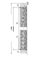
- Reference numerals 901 to 904 in the waveform of the OFDM signal shown in FIG. 25 are similar to the waveform of the OFDM signal shown in FIG. 23, reference numeral 905 represents a reduced waveform region of the OFDM signal, reference numerals 906 and 907 represent pilot signals, and reference numeral 908. And 909 represent empty subcarriers.
- the subcarrier 902 including the user data is limited to the area of the reduced effective bandwidth W ′′ smaller than the effective bandwidth W ′, and the effective bandwidth W ′ and the reduced effective bandwidth W Are used as unused free subcarriers, while pilot signals 906 and 907 are arranged on subcarriers at both ends of the effective bandwidth W ′.
- ⁇ k (t) for phase noise correction is obtained. That is, the effective bandwidth W 'within ⁇ W' / 2 from the center frequency is used for communication, and the subcarriers at both ends are assigned to pilot signals 906 and 907, and the subcarrier number is ⁇ K / 2. K is the number of subcarriers within the effective bandwidth W '. Further, the area of the subcarriers 908 and 909 between ⁇ W ′ / 2 and ⁇ W ′′ / 2 inside the area is an empty subcarrier, and no user data or the like is allocated, and the area within ⁇ W ′′ / 2 from the center frequency is not allocated. , A frequency domain for transmitting user data is allocated.
- FIG. 26 shows the relationship between the transmission training signal and its received waveform.
- 26A shows a transmission training signal on the transmission side
- FIG. 26B shows a reception waveform on the reception side.
- reference numeral 906 denotes a training signal on the transmitting side
- 903 and 908 denote subcarriers around the training signal
- 911 denotes a training signal on the receiving side
- 912 and 913 denote leaked training signals.
- a predetermined signal is assigned to subcarrier numbers ⁇ K / 2 at both ends of ⁇ W ′ / 2 from the center frequency
- a signal is assigned to subcarriers in an area of ⁇ W ′ / 2 to ⁇ W ′′ / 2. Shall not be performed.
- training signal 906 shown in FIG. 26A is subcarrier-K / 2
- subcarrier 903 in FIG. 25 corresponds to a guard band
- subcarrier 908 corresponds to an empty subcarrier.
- No signal is assigned to the subcarrier 903 and subcarrier 908 areas.
- the leaked training signal 912 leaks to the subcarrier 903 area
- the leaked training signal 913 leaks to the subcarrier 908 area.
- the training signal 911 is also in a state where the amplitude of the training signal 906 and the rotation of the complex phase are added to the training signal 906 of the transmission signal.
- the transmitted signal of each subcarrier is affected by the phase noise of the local oscillator of the transmitting and receiving station, and as shown in FIG. It leaks to the carrier, but the way of this leak is common to all subcarriers.
- Pilot signal 906 similarly leaks to adjacent subcarriers, but since there is no assignment to subcarriers on both sides of this pilot signal, it is possible to recognize the state of leakage from the pilot signal using this empty subcarrier.
- FIG. 27 shows the relationship between the waveforms of the transmission signal and the reception signal.
- FIG. 27A shows a transmission signal on the transmission side
- FIG. 27B shows a reception signal on the reception side.
- reference numeral 902 denotes a signal of an individual subcarrier
- reference numeral 905 denotes a waveform region of a reduced OFDM signal
- reference numerals 906 and 907 represent pilot signals
- reference numerals 911 and 915 represent training signals on the reception side
- reference numeral 914 represent the waveforms of the leakage signal from the pilot signal
- 917 and 918 represent the regions corresponding to FIG. 26
- 919 represents the signal of the individual subcarrier on the receiving side
- 920 represents the individual subcarrier and the individual 5 shows a waveform of a leakage signal from a subcarrier.
- ⁇ W '/ 2 and ⁇ W''/ if between 2 and had free subcarrier of 2N PN present center frequency side of the N PN book of unused sub-carrier user data of half of subcarriers Is strongly affected by the leakage from the effective subcarriers used for transmission (corresponding to the subcarriers including user data and the leakage signal 920), but the signals detected by the remaining outer NPN free subcarriers are at both ends.
- the waveforms 914 and 916 of the leakage signal from the pilot signal can be regarded as being strongly received.
- guard band regions 917 and 918 is considered a leakage component of the signal component detected pilot signals at both ends and on both sides the N PN book free subcarrier from the pilot signal as in FIG. 26,
- the description of “including the guard band” means that the subcarrier number to which a valid signal is assigned is ⁇ K / 2 to + K / 2 (excluding the center frequency) in Equation (2). The result of the FFT in the guard band region exceeding the above is effectively used.
- the transfer function h k + k ′ and the transfer function h k are calculated in the calculation of the coefficient ⁇ k + k ′ / ⁇ k. It is canceled between the denominator and the numerator, and coincides with the coefficient ⁇ k + k ′ / ⁇ k independent of the transfer function. Therefore, the function ⁇ k (t) of the equation (5) can be obtained from the pilot signal and the output information from the FFT for a total of (2N PN +1) subcarriers adjacent thereto.
- the received signals of the subcarriers constituting the OFDM signal including phase noise are individually obtained. Phase noise compensation is performed, and as a result, inter-subcarrier interference of all subcarriers can be eliminated. After the inter-subcarrier interference is once compensated in this way, a signal in the frequency domain free of the inter-subcarrier interference can be extracted by FFT of this signal.
- phase noise compensation processing is also required. That is, in all OFDM symbols including the preamble signal, the above-described phase noise compensation processing in symbol units (* Note: FFT processing is also incorporated in the phase noise compensation processing) is performed by FFT for signal detection processing. Prior to the processing, the FFT and the subsequent normal signal detection processing are performed on the converted sampling signal subjected to the phase noise compensation.
- the wavelength is the speed of light c (3 ⁇ 10 8 m in the frequency components of its ends f k-NPN and k + NPN / S) so as to be c / f k-NPN and c / f k + NPN .
- the complex phase rotation amount is 2 ⁇ ⁇ L ⁇ f k ⁇ NPN / c and 2 ⁇ ⁇ L ⁇ f k + NPN / c while propagating the distance L at each wavelength.
- the difference is 4 ⁇ ⁇ L ⁇ ⁇ f ⁇ N PN / C. If this value is sufficiently small, the above approximation holds, but if the value is a constant level, the above approximation is broken.
- the complex phase of the k-th subcarrier of frequency f k is given by L ⁇ f k / c at a point of distance L. Rotates in proportion to the frequency. Taking the frequency in the horizontal direction and the amount of complex phase rotation in the vertical direction and drawing a graph of the frequency dependence of the complex phase rotation amount, it can be represented by a monotonic linear order. In the radio signal processing, it does not affect the characteristic degradation as frequency selective distortion, but even in such a flat channel with only direct waves, this complex phase rotation is ignored in the above-described phase noise compensation. It may not be possible.
- the center frequency f when the bandwidth is W in c the most complex phase rotation amount of the wavelength at the shorter f c + W / 2 2 ⁇ ⁇ L ⁇ (f c + W / 2) / c and most long wavelength f
- the difference from the complex phase rotation amount 2 ⁇ ⁇ L ⁇ (f c ⁇ W / 2) / c at c + W / 2 is 2 ⁇ ⁇ L ⁇ W / c.
- N p L ⁇ W / c.
- phase noise compensation channel complex phase rotation of 2 [pi ⁇ N p occurs over the entire band were then processed approximated last constants (complex phase rotation free)
- a replica of the estimated phase noise signal is determined as N p samples delayed waveforms. If gradual time variation of phase noise, but this delay of N p samples not appear as a significant deviation from the actual waveform of the time variation of the phase noise, a relatively steep time variation of phase noise N p samples If there is a non-negligible phase fluctuation during the delay, the phase shift due to appropriate phase noise cannot be compensated without this correction, and as a result, sufficient phase noise compensation effect may not be obtained. There is. In such a case, there is a problem that the throughput decreases due to the inter-subcarrier interference.
- an object of the present invention is to provide a technique capable of suppressing a decrease in throughput due to inter-subcarrier interference in wireless transmission using a high frequency band such as a millimeter wave.
- One embodiment of the present invention is a wireless communication device in a wireless communication system including a first wireless communication device and a second wireless communication device, wherein the first wireless communication device has a predetermined bandwidth within an effective bandwidth.
- a frequency region as an empty region, a transmission signal generating means for generating a transmission signal including information to be transmitted in an area or a part of the effective bandwidth except for the empty area, and a predetermined signal in the effective bandwidth.
- a pilot signal generating means for generating a pilot signal without an effective signal component in an adjacent frequency component and adding the pilot signal to the transmission signal generated by the transmission signal generating means, and a pilot signal generated by the pilot signal applying means.
- Transmitting means for transmitting, at a radio frequency, a transmission signal including the pilot signal
- the second radio communication apparatus comprises: Receiving means for receiving a signal; time / frequency signal converting means for converting a signal received by the receiving means or a signal obtained by frequency-converting the signal from a time-domain sampling signal to a frequency-domain signal; Means for setting an approximate value L 'of the distance between the wireless communication device and the first wireless communication device, an approximate value L' of the distance, an effective bandwidth W, a light speed c, and the time / frequency converting means.
- a frequency domain signal including a component and a plurality of peripheral frequency components including at least adjacent frequency components of the pilot signal is extracted, and a coefficient for each frequency component of the extracted signal and a previous signal are extracted.
- a phase noise replica generating means for generating a replica of the phase noise based on the coefficient gamma k, and a replica of the phase noise, the sampling signal is modified based on the sampling signal or a sampling signal of the time domain of the time domain and Phase noise compensating means for generating a sampling signal compensated for phase noise by using the phase noise compensating means, and data reproduction for reproducing data transmitted from the first wireless communication apparatus based on an output signal from the phase noise compensating means.
- a wireless communication device for generating a replica of the phase noise based on the coefficient gamma k, and a replica of the phase noise, the sampling signal is modified based on the sampling signal or a sampling signal of the time domain of the time domain.
- pilot signal assigning means assigns a pilot signal subcarrier to both ends or one of the frequency components of the effective bandwidth
- the surrounding subcarriers including the carrier are set as empty subcarriers.
- One embodiment of the present invention is the above wireless communication apparatus, wherein the pilot signal providing unit is configured to perform one cycle of a sine wave signal having a predetermined frequency or a combined signal of a plurality of sine wave signals having a predetermined frequency or an integral multiple thereof.
- phase noise replica generation means is a positive integer NPN equal to or greater than 1 and an integer k ′ that satisfies ⁇ NPN ⁇ k ′ ⁇ NPN .
- the time / frequency signal based on the 'factor beta k + k of the frequency component coefficient beta k and a (k + k)' of the pilot signal of the k frequency component obtained by the conversion means, the sampling data at time t of the formula ( 5)
- the sampling data given by the reciprocal is generated as a replica of the phase noise.
- phase noise replica generation means is a positive integer NPN equal to or greater than 1 and an integer k ′ that satisfies ⁇ NPN ⁇ k ′ ⁇ NPN .
- the time / based on 'factor beta k + k of the frequency component coefficient beta k and a (k + k)' of the pilot signal of the k frequency component acquired by frequency signal converting means the following equation sampling data at time t ( 8) and the sampling data given by the reciprocal of Expression (12) or Expression (8) is generated as a replica of the phase noise.
- phase noise compensating means further includes a removing means for removing the pilot signal and a predetermined frequency component around the pilot signal from a received signal.
- One embodiment of the present invention is a wireless communication method performed by a wireless communication device in a wireless communication system including a first wireless communication device and a second wireless communication device, wherein the first wireless communication device has an effective band.
- a pilot signal providing step wherein the first wireless communication apparatus transmits the pilot signal including the pilot signal generated by the pilot signal providing step.
- a decrease in throughput due to interference between subcarriers due to phase noise can be suppressed. Further, even when the distance between the two wireless station devices is relatively long, it is possible to avoid the influence of the frequency dependence of the channel due to the distance and to compensate for the phase noise.
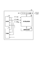
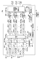
- FIG. 2 is a diagram illustrating a circuit configuration of the wireless station device according to the first embodiment.
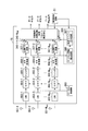
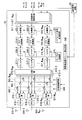
- FIG. 2 is a schematic block diagram illustrating an example of a configuration of a transmission unit of the wireless station device according to the first embodiment.
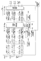
- FIG. 3 is a schematic block diagram illustrating an example of a configuration of a receiving unit of the wireless station device according to the first embodiment.
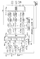
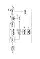
- FIG. 2 is a schematic block diagram illustrating an example of a configuration of an extended FFT circuit according to the first embodiment.
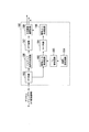
- FIG. 3 is a schematic block diagram illustrating another example of the configuration of the extended FFT circuit according to the first embodiment.
- FIG. 9 is a schematic block diagram illustrating an example of a configuration of a transmission unit of a wireless station device according to a second embodiment.
- FIG. 9 is a schematic block diagram illustrating an example of a configuration of a receiving unit of a wireless station device according to a second embodiment. It is a figure showing the schematic block diagram showing an example of the composition of the transmitting part of the radio station device in a 3rd embodiment. It is a figure showing the schematic block diagram showing an example of the composition of the receiving part of the radio station device in a 3rd embodiment.
- FIG. 14 is a diagram illustrating a configuration of an extended FFT circuit according to a fourth embodiment.
- FIG. 14 is a schematic block diagram illustrating another example of the configuration of the extended FFT circuit according to the fourth embodiment.
- FIG. 14 is a diagram illustrating a configuration example of a single carrier compensation circuit according to a fifth embodiment.
- FIG. 14 is a diagram illustrating another configuration example of the single carrier compensation circuit according to the fifth embodiment. It is a figure showing the schematic block diagram showing an example of the composition of the transmitting part at the time of single carrier transmission in a 5th embodiment. It is a figure showing the schematic block diagram showing an example of the composition of the receiving part at the time of single carrier transmission in a 5th embodiment. It is a figure showing the outline of the opposite radio station device in a 6th embodiment.
- FIG. 11 is a diagram illustrating a circuit configuration of a conventional wireless station device.
- FIG. 3 is a schematic block diagram illustrating an example of a configuration of a transmission unit in the wireless station device.
- FIG. 3 is a schematic block diagram illustrating an example of a configuration of a receiving unit in the wireless station device.
- FIG. 9 is a schematic block diagram illustrating an example of a configuration of a transmission unit of a wireless station device in Non-Patent Document 1.
- FIG. 9 is a schematic block diagram illustrating an example of a configuration of a receiving unit of a wireless station device in Non-Patent Document 1.
- FIG. 9 is a schematic block diagram illustrating an example of a configuration of a transmission unit of a wireless station device in Non-Patent Document 2.
- FIG. 9 is a diagram illustrating a specific example of a waveform of an OFDM signal in the related art.
- FIG. 9 is a schematic block diagram illustrating an example of a configuration of a receiving unit of a wireless station device in Non-Patent Document 2.
- FIG. 9 is a schematic block diagram illustrating an example of a configuration of a receiving unit of a wireless station device in Non-Patent Document 2.
- FIG. 9 is a diagram illustrating a specific example of a waveform of an OFDM signal in the related art.
- FIG. 7 is a diagram illustrating a relationship between a transmission training signal and a reception waveform thereof in the related art.
- FIG. 6 is a diagram illustrating a relationship between waveforms of a transmission signal and a reception signal in the related art.
- the root cause of the above problem is that the term of phase rotation proportional to the distance is included in the channel information used for estimating the phase noise. For example, assuming that the approximate value of the distance between the two wireless station apparatuses is L ′, the phase rotation amount proportional to the distance can be canceled by the coefficient ⁇ k for the subcarrier number k shown in the following equation (10).
- the distance may be measured directly using a laser pointer-type distance measuring device, or may be calculated based on information on the installation location. In any case, if the distance can be obtained with an error of about several percent, the time lag of the replica of the phase noise will be significantly corrected.
- the coefficient obtained in this manner can be used by replacing, for example, equation (5) as in equation (11) below.
- the coefficient ⁇ k is calculated so that the receiving-side radio station device cancels the phase rotation amount proportional to the distance as described above. Then, the receiving-side radio station apparatus generates a replica signal of phase noise using the calculated coefficient ⁇ k and a coefficient for each frequency component of the signal, and uses the generated replica signal of phase noise to generate a phase rotation amount. Cancel The above-described problem is solved by performing such processing.
- the OFDM modulation method will be described as a typical example, but expansion is possible in other single carrier transmissions, and this point will be described later.
- the transmission weight and the reception weight in the time domain are also expressed as a time-axis transmission weight and a time-axis reception weight, but these terms "time axis" and "time domain” have the same meaning. .
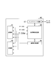
- FIG. 1 is a diagram illustrating a circuit configuration of a wireless station device 70 according to the first embodiment.
- the wireless station device 70 includes a transmitting unit 71, a receiving unit 75, an interface circuit 67, a MAC (Medium Access Control) layer processing circuit 68, and a communication control circuit 51.
- the wireless station device 70 inputs and outputs data to and from an external device or a network via the interface circuit 67.
- the interface circuit 67 detects data to be transferred on the wireless line from the input data, and outputs the detected data to the MAC layer processing circuit 68.
- the MAC layer processing circuit 68 performs processing related to the MAC layer in accordance with an instruction from the communication control circuit 51 that performs management control of the operation of the entire wireless station device 70.
- signals are spatially multiplexed and transmitted to one wireless station device 70, so that a plurality of signal sequences are output from the MAC layer processing circuit 68 to the transmission unit 71.
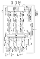
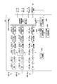
- FIG. 2 is a schematic block diagram illustrating an example of a configuration of the transmission unit 71 of the wireless station device 70 according to the first embodiment.
- the transmission unit 71 includes transmission signal processing circuits 311-1 to 311-N SDM , addition and synthesis circuits 812-1 to 812-N Ant , and IFFT & GI addition circuits 813-1 to 812-N Ant.
- the transmission signal processing circuits 311-1 to 311- NSDM and the transmission weight processing unit 840 are connected to the communication control circuit 51.
- the transmission weight processing section 840 includes a channel information acquisition circuit 841, a channel information storage circuit 842, and a transmission weight calculation circuit 843.
- N SDM subscripts of the transmission signal processing circuits 311-1 ⁇ 311-N SDM in FIG. 2 represents a multiplex number for performing spatial multiplexing simultaneously.
- the fact that NSDM is the number of multiplexes that perform spatial multiplexing simultaneously is the same in the following embodiments.
- N Ant subscripts circuit from additive synthesis circuits 812-1 ⁇ 812-N Ant to the antenna elements 819-1 ⁇ 819-N Ant represents the number of antenna elements provided in the radio station 70.
- the fact that N Ant is the number of antenna elements included in the wireless station device 70 is the same in the following embodiments.
- the transmission signal processing circuits 311-1 to 311-N SDM include a transmission signal processing circuit for generating an OFDM signal having an effective bandwidth W ′ shown in FIG. 23 and an OFDM signal having a reduced effective bandwidth W ′′ shown in FIG. The difference is that the signal is generated, and the other functions are the same.
- the transmission signal processing circuits 311-1 to 311-N SDM perform signal processing of the reduced effective bandwidth W ′′, the transmission weights input from the transmission weight processing unit 840 are only for the subcarriers to which the assignment is made. It is.
- one radio station apparatus 70 spatially multiplexes a signal to another radio station apparatus 70 and transmits the signal
- a plurality of signal sequences are input from the MAC layer processing circuit 68 to the transmission unit 71 and input.
- signal series of a plurality of systems is input to the transmission signal processing circuits 311-1 ⁇ 311-N SDM.
- the transmission signal processing circuits 311-1 to 311-N SDM transmit data (data inputs # 1 to #N SDM ) to be transmitted to the destination wireless station device 70 from the MAC layer processing circuit 68 via the wireless line (wireless).
- a modulation process is performed on the packet.
- the signal of each signal sequence is subjected to modulation processing for each subcarrier within the reduced effective bandwidth W ′′ shown in FIG.
- the transmission signal processing circuits 311-1 to 311-N SDM multiply the baseband signal subjected to the modulation processing by the transmission weight for each subcarrier.
- the signal multiplied by the transmission weight corresponding to each of the antenna elements 819-1 to 819-N Ant is subjected to the remaining signal processing as necessary, and is processed as a signal in the frequency domain of the transmission signal in the baseband.
- Circuits 311-1 to 311-N are input to the addition / synthesis circuits 812-1 to 812-N Ant from the SDM .
- the signals input to the addition / combination circuits 812-1 to 812-N Ant are combined for each subcarrier.
- the synthesized signal is converted from a signal on the frequency axis to a signal on the time axis by IFFT & GI adding circuits 813-1 to 813-N Ant , and furthermore, a guard interval is inserted and an OFDM symbol interval (for SC-FDE, Processing such as waveform shaping (between blocks of block transmission) is performed.
- Pilot signal sampling data is output from pilot signal storage circuit 321 and added to output signals from IFFT & GI adding circuits 813-1 to 813-N Ant by adders 320-1 to 320-N Ant .
- Sampling data is repeatedly output from pilot signal storage circuit 321 in such a manner that each sine wave waveform of the pilot signal is continuous.
- the signals added by the adder are converted from digital sampling data to baseband analog signals by D / A converters 814-1 to 814-N Ant for each system of the antenna elements 819-1 to 819-N Ant. Is converted. Further, each analog signal is multiplied by a local oscillation signal input from the local oscillator 815 by the mixers 816-1 to 816-N Ant and is up-converted into a radio frequency signal.
- the up-converted signal includes a signal in an out-of-band region of a channel to be transmitted, the out-of-band signal is removed by filters 817-1 to 817-N Ant and the signal to be transmitted is removed.
- the generated signal is amplified by high power amplifiers 818-1 to 818-N Ant and transmitted from antenna elements 819-1 to 819-N Ant .
- processing such as IFFT processing, insertion of a guard interval, and waveform shaping is performed.
- the transmission signal processing circuits 311-1 to 311-N SDM perform these processes, and the IFFT & GI addition circuit is configured to synthesize the IFFT-sampled signals on the time axis by the addition and synthesis circuits 812-1 to 812-N Ant.
- a configuration in which 813-1 to 813-N Ant are omitted may be adopted.
- the remaining signal processing as needed after transmission weight multiplication in the transmission signal processing circuits 311-1 to 311-N SDM refers to processing such as IFFT processing, insertion of a guard interval, and waveform shaping.
- the transmission weight multiplied by the transmission signal processing circuits 311-1 to 311-N SDM is obtained from the transmission weight calculation circuit 843 provided in the transmission weight processing unit 840 during the signal transmission processing.
- the channel information acquisition circuit 841 separately acquires the channel information acquired by the reception unit 75 via the communication control circuit 51, and sequentially updates the acquired channel information in the channel information storage circuit 842.
- the transmission weight calculation circuit 843 reads channel information corresponding to the destination station from the channel information storage circuit 842 and calculates a transmission weight based on the read channel information in accordance with an instruction from the communication control circuit 51.
- Transmission weight calculating circuit 843 outputs the calculated transmission weight to the transmission signal processing circuits 311-1 ⁇ 311-N SDM. If the wireless station device is a base station, the communication control circuit 51 communicates with a plurality of terminal station devices, and thus manages which terminal station device is the destination station.
- the signals of the N SDM system output from the transmission signal processing circuits 311-1 to 311-N SDM are combined by the addition / combination circuits 812-1 to 812-N Ant and the subsequent D / A converter 814-1.
- 814-N Ant to the antenna elements 819-1 to 819-N Ant are shared, but the following D / A converters 814 are individually combined without being combined by the addition combining circuits 812-1 to 812-N Ant .
- 1 to 814-N Ant to antenna elements 819-1 to 819-N Ant may be mounted, and a sub-array may be configured by antenna elements 819-1 to 819-N Ant in each.
- a virtual transmission path corresponding to the first singular value is used between the wireless station device 70 and the array antenna or sub-sale in the transmitting unit 71 and the receiving unit 75 of the wireless station device 70. It is also possible. There are several variations in the channel estimation method and the transmission / reception weight calculation method when utilizing the virtual transmission path corresponding to the first singular value. For example, for each channel matrix from the wireless station device 70 to the antenna elements 819-1 to 819-N Ant of another wireless station device 70, the first right singular vector obtained when the singular value decomposition is performed is used as the transmission weight vector. May be used. In this case, the transmission weight calculation circuit 843 has a function of calculating the first right singular vector. Alternatively, various methods for obtaining an approximate solution of such a singular vector may be used.
- the transmission weight calculation circuit 843 has a function of calculating the first right singular vector.
- various methods for obtaining an approximate solution of such a singular vector may be used.
- the provision of the pilot signals at both ends of the effective bandwidth is performed by the adder 320-1 between the IFFT & GI provision circuits 813-1 to 813-N Ant and the D / A converters 814-1 to 814-N Ant.
- 320320-N Ant in the transmission signal processing circuits 311-1 ⁇ 311-N SDM , a signal in which pilot signals are assigned to subcarriers at both ends of the effective bandwidth is generated and transmitted.
- a configuration may be adopted in which predetermined signal processing such as weight multiplication is performed. In this case, the adders 320-1 to 320-N Ant and the pilot signal storage circuit 321 become unnecessary, and equivalent processing is performed in the transmission signal processing circuits 311-1 to 311-N SDM .
- FIG. 3 is a schematic block diagram illustrating an example of a configuration of the receiving unit 75 of the wireless station device 70 according to the first embodiment.
- the reception unit 75 includes antenna elements 851-1 to 851-N Ant , low noise amplifiers (LNA) 852-1 to 852-N Ant , a local oscillator 853, and mixers 854-1 to 854.
- -N Ant filters 855-1 to 855-N Ant , A / D (analog / digital) converters 856-1 to 856-N Ant , extended FFT circuits 357-1 to 357-N Ant , and reception Signal processing circuits 345-1 to 345- NSDM and a reception weight processing unit 844 are provided.
- the reception signal processing circuits 345-1 to 345- NSDM and the reception weight processing section 844 are connected to the communication control circuit 51 shown in FIG.
- the reception weight processing section 844 includes a channel information estimation circuit 846 and a reception weight calculation circuit 847.
- the signals received by the antenna elements 851-1 to 851-N Ant are amplified by the low noise amplifiers 852-1 to 852-N Ant .
- the amplified signal and the local oscillation signal output from the local oscillator 853 are multiplied by mixers 854-1 to 854-N Ant , and the amplified signal is down-converted from a radio frequency signal to a baseband signal. Since the down-converted signal includes a signal outside the frequency band to be received, the out-of-band component is removed by the filters 855-1 to 855-N Ant .
- the signals from which the out-of-band components have been removed are converted into digital baseband signals by A / D converters 856-1 to 856-N Ant .
- Enhanced FFT circuits 357-1 ⁇ 357-N Ant when using OFDM, together with digital baseband signal is input to the extended FFT circuits 357-1 ⁇ 357-N Ant, implementing the phase noise compensation processing described later Enhanced FFT circuits 357-1 ⁇ 357-N Ant
- a signal on the time axis is converted into a signal on the frequency axis (separated into signals of each subcarrier) at a predetermined symbol timing determined by a timing detection circuit not shown.
- the signals separated into the respective subcarriers are input to the reception signal processing circuits 345-1 to 345-N SDM and also input to the channel information estimation circuit 846.
- the antenna elements 819-1 to 819-N on the transmitting station side are based on the known signal for channel estimation (such as a preamble signal added to the head of a radio packet) separated into each subcarrier. to estimate the channel vector of the channel information between the Ant and the antenna elements 851-1 ⁇ 851-N Ant the receiving station for each subcarrier, and outputs the estimation result to the reception weight calculating circuit 847.
- the reception weight calculation circuit 847 calculates the reception weight to be multiplied for each subcarrier based on the input channel information.
- reception weight for example, as described above, a ZF type pseudo inverse matrix is used, or an MMSE type reception weight matrix is used.
- the reception weight vector for synthesizing the signals received by the antenna elements 851-1 to 851-N Ant differs for each signal sequence, and the above-described ZF-type pseudo inverse matrix or MMSE-type reception weight matrix is used. corresponds to a row vector like are input to the reception signal processing circuit 345-1 ⁇ 345-N SDM corresponding to the signal sequence to be extracted.
- reception signal processing circuits 345-1 to 345-N SDM the signal for each subcarrier input from the extended FFT circuits 357-1 to 357-N Ant is multiplied by the reception weight input from the reception weight calculation circuit 847. Then, the signals received by the antenna elements 851-1 to 851-N Ant are added and synthesized for each subcarrier.
- the reception signal processing circuits 345-1 to 345-N SDM perform demodulation processing on the signals obtained by addition and synthesis, and output the reproduced data to the MAC layer processing circuit 68.
- different received signal processing circuits 345-1 to 345-N SDM perform signal processing of different signal sequences.
- MLD simple MLD using QR decomposition, or the like may be used.
- the MAC layer processing circuit 68 performs processing related to the MAC layer (for example, conversion between data input / output to / from the interface circuit 67 and data transmitted / received on the wireless line, ie, wireless packets, termination of MAC layer header information). Do).
- the received data processed by the MAC layer processing circuit 68 is output to an external device or a network via the interface circuit 67.
- the communication control circuit 51 manages control related to overall communication such as overall timing control.
- the reception unit 75 shares the antenna elements 851-1 to 851-N Ant to the extended FFT circuits 357-1 to 357-N Ant , and the extended FFT circuits 357-1 to 357-N Ant.
- the output from the N Ant is copied to the N SDM system and input to the individual reception signal processing circuits 345-1 to 345-N SDM , but the extended FFT circuit 357- is transmitted from the antenna elements 851-1 to 851-N Ant.
- 1 to 357-N Ant can be individually mounted, and each antenna element 851-1 to 851-N Ant can be realized in a sub-array configuration.
- a virtual transmission path corresponding to the first singular value is used between the wireless station device 70 and the array antenna or sub-sale in the transmitting unit 71 and the receiving unit 75 of the wireless station device 70. It is also possible. There are several variations in the channel estimation method and the transmission / reception weight calculation method when utilizing the virtual transmission path corresponding to the first singular value. For example, for each channel matrix from another wireless station device 70 toward its own antenna elements 819-1 to 819-N Ant , the first left singular vector obtained by performing singular value decomposition is used as a reception weight vector. Is also good. In this case, the reception weight calculation circuit 847 has a function of calculating the first left singular vector. Alternatively, various methods for obtaining an approximate solution of such a singular vector may be used.
- FIG. 4 is a schematic block diagram illustrating an example of the configuration of the extended FFT circuit 357 according to the first embodiment.
- a block 180 (FIG. 4A) corresponding to a functional block of the conventional FFT circuit is changed to a block 190 in the extended FFT circuit in the first embodiment (FIG. 4B )).
- the extended FFT circuit 357 includes a duplication circuit 181, an FFT circuit 182, a function ⁇ (t) acquisition circuit 183, an IFFT circuit 184, a phase noise compensation circuit 185, a ⁇ k setting circuit 193, and a distance.
- An L setting circuit 194 and an FFT circuit 857 are provided.
- the extended FFT circuit 357 is connected to the reception signal processing circuit 345, the reception weight processing unit 844, and the A / D converter 856 in FIG.
- the installer calculates an approximate value L ′ of the distance between the two wireless station devices by some method, and sets this by the distance L setting circuit 194. .
- a numerical value input means may be provided on the device, or another device for control (PC or the like) may be connected and the setting may be made from the outside.
- the set distance L as ' is input to the gamma k setting circuit 193, gamma k setting circuit 193 in the L' was used to calculate the gamma k by equation (10), which function [Phi (t) acquired
- the signal is input to the circuit 183 and is prepared in advance.
- the digital sampling data is input from the A / D converter 856 to the extended FFT circuit 357 (block 190), the sampling data is duplicated by the duplication circuit 181, one is the FFT circuit 182, and the other is the phase.
- the signal is input to the noise compensation circuit 185.
- the FFT circuit 182 performs FFT on the sampling data cut out at a predetermined symbol timing determined by a timing detection unit not shown in the figure, and extracts components related to the pilot signal in FIG. 3 and subcarrier areas 917 and 918 in the vicinity thereof. Then, this information is input to the function ⁇ (t) acquisition circuit 183.
- the function ⁇ (t) acquisition circuit 183 calculates the value corresponding to the coefficient ⁇ k + k ′ ⁇ ⁇ k + k ′ / ⁇ k of the function ⁇ k (t) in equation (5) based on the output of the FFT circuit 182 by the above-described method. Is calculated by the above-described calculation of the coefficient ⁇ k + k ′ ⁇ ⁇ k + k ′ / ⁇ k . As a result, the coefficient in the frequency domain of the reciprocal of the function ⁇ (t) is obtained.
- the IFFT circuit 184 converts the signal in the frequency domain into a signal in the time domain, and inputs the signal in the time domain to the phase noise compensation circuit 185.
- the reciprocal of the time domain signal input from the IFFT circuit 184 that is, the function ⁇ (t)
- the time domain signal input from the duplication circuit 181 strictly, the FFT
- the value of the implemented time interval signal corresponding to the area from which the guard interval has been removed is multiplied by each sampling data as shown in Expression (6), and the signal in the time domain in which phase noise compensation has been performed is reproduced.
- the reproduced time-domain signal (sampling data) is input to the FFT circuit 857, where it is converted from a time-domain signal to a frequency-domain signal again.
- the signal in this frequency domain is a signal in which phase noise has been compensated, and power leakage between subcarriers is suppressed.
- the signal in the frequency domain is input to the reception signal processing circuit 345, where predetermined reception signal processing is performed.
- the signal processing performed by the reception signal processing circuit 345 is basically equivalent to the conventional reception signal processing circuit, whereas the conventional reception signal processing circuit processes an OFDM signal having an effective bandwidth W ′ shown in FIG.
- the reception signal processing of the reduced effective bandwidth W ′′ shown in FIG. 25 is performed.
- the processing is performed ignoring the pilot signal and the signal components in the empty subcarrier area, they are strictly shown as different functional blocks. However, only the effective subcarrier range is different, and other signal processing is not performed at all. It is equivalent. Therefore, the output of information to the reception weight processing section 844 is completely equivalent to the conventional configuration except that the effective bandwidth W 'is changed to the reduced effective bandwidth W' '.
- FIG. 5 As another configuration that achieves the same effect, the configuration of FIG. 5 in which the processing is performed by Expression (12) instead of Expression (11) may be used.
- a function ⁇ (t) acquisition circuit 195 and a function ⁇ (t) acquisition circuit 196 are added to FIG. 4 and the function ⁇ (t) acquisition circuit 183 is deleted.
- FIG. 5 is the same as FIG. 4 up to the point where ⁇ k is calculated by equation (10), except that this result is input to the function ⁇ (t) acquisition circuit 195 and is prepared in advance.
- the FFT circuit 182 performs FFT on sampling data cut out at a predetermined symbol timing determined by a timing detection unit not shown in the figure, and obtains a pilot signal in FIG. Components related to the regions 917 and 918 are extracted, and this information is input to the function ⁇ (t) acquisition circuit 195.
- the function ⁇ (t) acquisition circuit 195 calculates a value corresponding to the coefficient ⁇ k + k ′ ⁇ ⁇ k + k ′ of the function ⁇ k (t) in equation (12) based on the output of the FFT circuit 182. As a result, the frequency domain coefficient of the function ⁇ (t) is obtained.
- the IFFT circuit 184 converts the signal in the frequency domain into a signal in the time domain, and inputs this to the function ⁇ (t) acquisition circuit 196.
- the function ⁇ (t) acquisition circuit 196 calculates the function ⁇ (t) using Expression (8), and inputs the signal in the time domain to the phase noise compensation circuit 185.
- Other processes are the same as those in FIG.
- the measurement may be performed by some method (for example, the measurement may be performed directly using a laser pointer-type distance measurement device, or may be calculated based on information on the installation location).
- the phase rotation amount is canceled using the obtained approximate value of the distance between the two wireless station devices 70.
- the configuration of the wireless station device 70 is equivalent to the configuration of the wireless station device 70 shown in FIG.
- the only difference from FIG. 1 is that the transmitting unit 71 is replaced by the transmitting unit 72a, the receiving unit 75 is replaced by the receiving unit 76a, and the communication control circuit 51 is replaced by the communication control circuit 52.
- the features are the same as those in FIG. 1, and the details of the drawings and description are omitted here.
- FIG. 6 is a schematic block diagram illustrating an example of the configuration of the transmission unit 72a of the wireless station device 70 according to the second embodiment.
- the transmission unit 72a includes transmission signal processing circuits 411-1 to 411-N SDM , addition and synthesis circuits 812-1 to 812-N Ant , and IFFT & GI addition circuits 313-1 to 313-N SDM , D / A converters 814-1 to 814-N Ant , local oscillator 815, mixers 816-1 to 816-N Ant , filters 817-1 to 817-N Ant , and high power amplifier 818-1 To 818-N Ant , antenna elements 819-1 to 819-N Ant , transmission weight processing section 740, time axis transmission weight multiplication circuits 761-1 to 761-N SDM , and adders 420-1 to 420- An NSDM and a pilot signal storage circuit 321 are provided.
- the transmission weight processing unit 740 includes a channel information acquisition circuit 741, a channel information storage circuit 742, and a time axis transmission weight calculation circuit 743.
- the difference between FIG. 6 and the configuration of the transmission unit described in Non-Patent Document 1 is that the difference between the IFFT & GI addition circuits 313-1 to 313-N SDM and the time axis transmission weight multiplication circuits 761-1 to 761-N SDM Adders 420-1 to 420-N SDM are arranged, and a pilot signal storage circuit 321 is further added, and transmission signal processing circuits 711-1 to 711-N SDM are added to transmission signal processing circuits 411-1 to 411. it is that it is changed to -N SDM.
- the transmitting section 72a in FIG. 6 performs a process of adding pilot signals at both ends of the effective bandwidth W ′ to the transmission signal for each antenna system while performing an operation equivalent to the transmitting section in Non-Patent Document 1. Instead, the process is changed to a process of adding a pilot signal for each signal sequence to be spatially multiplexed.
- the transmission signal processing circuit in Non-Patent Document 2 generates a signal in which user data is allocated within the effective bandwidth W ′ shown in FIG. 25, FIG. 26 shows the reduced effective bandwidth shown in FIG. This corresponds to being changed to generate a signal in which user data is assigned in W ′′.
- Non-Patent Document 1 processing corresponding to the process of multiplying the transmission weight is performed by time-axis transmission weight multiplying circuits 761-1 ⁇ 761-N SDM.
- time axis transmission weight multiplying circuits 761-1 ⁇ 761-N SDM adder 420 is performed at -1 ⁇ 420-N SDM, as in the first embodiment, in the transmission signal processing circuits 411-1 ⁇ in 411-N SDM, the pilot signal across the sub-carriers of the available bandwidth It may be configured to generate the assigned signal. In this case, the adders 420-1 to 420-N SDM and the pilot signal storage circuit 321 become unnecessary, and equivalent processing is performed in the transmission signal processing circuits 411-1 to 411-N SDM .
- the signals of the N SDM system output from the time axis transmission weight multiplication circuits 761-1 to 761-N SDM are synthesized by the addition and synthesis circuits 812-1 to 812-N Ant .
- the following D / A converters 814-1 to 814-N Ant to the antenna elements 819-1 to 819-N Ant are shared, but they are individually combined without being combined by the addition and combining circuits 812-1 to 812-N Ant .
- FIG. 7 is a schematic block diagram illustrating an example of the configuration of the receiving unit 76a of the wireless station device 70 according to the second embodiment.
- the receiving section 76a includes antenna elements 851-1 to 851-N Ant , low noise amplifiers 852-1 to 852-N Ant , a local oscillator 853, and mixers 854-1 to 854-N Ant. , Filters 855-1 to 855-N Ant , A / D converters 856-1 to 856-N Ant , extended FFT circuits 157-1 to 157-N SDM , and received signal processing circuits 445-1 to 445.
- reception weight processing section 744 receives the transmission signal from the communication control circuit 52.
- the reception weight processing section 744 includes a channel information estimation circuit 746 and a reception weight calculation circuit 747.
- FIG. 7 The difference between FIG. 7 and the configuration of the receiving unit described in Non-Patent Document 1 is that FFT circuits 257-1 to 257-N SDM are changed to extended FFT circuits 157-1 to 157-N SDM. The difference is that the reception signal processing circuits 745-1 to 745-N SDM are changed to the reception signal processing circuits 445-1 to 445-N SDM .
- the FFT circuits 257-1 to 257-N SDM are changed to extended FFT circuits 157-1 to 157-N SDM , and the reception signal processing circuits 845-1 to 845-N SDM are further changed. is the same as that it is changed to the received signal processing circuits 345-1 ⁇ 345-N SDM.
- the reception unit 76a of FIG. 7 in that the receiving unit 66a and the equivalent operation of FIG. 21, the FFT circuit 257-1 ⁇ 257-N SDM, the pilot signals at both ends of the effective band width W 'to the transmission signal using an additional function to implement the phase noise compensation (corresponding to the expansion FFT circuits 157-1 ⁇ 157-N SDM), further, the received signal processing circuits 745-1 ⁇ 745-N in SDM 23 in FIG. 21 While the received signal processing is performed on the signal to which the user data is allocated within the effective bandwidth W ′ shown in FIG. 7, the user data is allocated within the reduced effective bandwidth W ′′ shown in FIG. 25 in FIG. This corresponds to that the received signal has been changed to perform the received signal processing. Further, other features are the same as the description of the receiving unit 66a in Non-Patent Document 1 shown in FIG.
- the same effects as those of the first embodiment can be obtained in another configuration.
- Non-Patent Document 1 digitally multiplies the time axis transmission weight at the time axis transmission weight multiplying circuits 761-1 ⁇ 761-N SDM, the time axis reception weight multiplication circuits 755-1 ⁇ 755- It was multiplied by the time-axis receiving weight digitally at N SDM.
- multiplication of the transmission / reception weights in the time domain is equivalent to multiplication of a common coefficient in all frequency bands, and this involves rotating the phase of an analog transmission signal or an analog reception signal directly using a phase shifter. This is equivalent to the following processing.
- Non-Patent Document 2 calculates transmission / reception weights to be digitally multiplied by the method described in Non-Patent Document 1, while processing corresponding to actual multiplication of time-axis transmission / reception weights is performed by phase shifting. The method used in the vessel is adopted.
- the third embodiment will be described as a difference therefrom.
- the configuration of the wireless station device is equivalent to the configuration of the wireless station device 70 shown in FIG.
- the only difference from FIG. 1 is that the transmitting unit 71 is replaced by the transmitting unit 72b, the receiving unit 75 is replaced by the receiving unit 76b, and the communication control circuit 51 is replaced by the communication control circuit 53.
- the features are the same as those in FIG. 1, and the details of the drawings and description are omitted here.
- FIG. 8 is a schematic block diagram illustrating an example of a configuration of the transmission unit 72b of the wireless station device 70 according to the third embodiment.
- the transmitting unit 72b is a transmission signal processing circuits 411-1 ⁇ 411-N SDM, the IFFT & GI imparting circuits 313-1 ⁇ 313-N SDM, D / A converters 414-1 ⁇ 414- N SDM , local oscillator 815, mixers 316-1 to 316-N SDM , filters 317-1 to 317-N SDM , high power amplifiers 818-1 to 818-N Ant , and antenna element 819-1 to 819-N Ant , combiners 671-1 to 671-N Ant , phase shifters 681-1 to 681-N SDM , distributors 673-1 to 673-N SDM , phase control circuit 688, A time axis transmission weight calculation circuit 642 and a pilot signal storage circuit 321 are provided.
- D / A converters 314-1 to 314-N SDM are changed to D / A converters 414-1 to 414-N SDM , and a pilot signal storage circuit 321 is further added.
- the transmission signal processing circuits 711-1 to 711-N SDM are changed to transmission signal processing circuits 411-1 to 411-N SDM .
- the D / A converters 414-1 to 414-N SDM add the time domain signals from the IFFT & GI adding circuits 313-1 to 313-N SDM and the time domain signals from the pilot signal storage circuit 321 for each sampling data.
- a function of performing D / A conversion on the added value is provided in the subsequent stage of the IFFT & GI adding circuits 313-1 to 313-N SDM (and the D / A converters 314-1 to 314-N
- This is equivalent to a configuration in which adders 420-1 to 420-N SDM are arranged in the same manner as in FIG. 8 (before the SDM ), and the time domain signal from the pilot signal storage circuit 321 is added for each sampling data.
- FIG. 18 and the differential of Figure 2 is, IFFT & GI imparting circuits 813-1 ⁇ 813-N Ant and D / A converters 814-1 ⁇ 814-N adder between the Ant 320-1 to 320-N Ant are added, and a pilot signal storage circuit 321 is further added, and the transmission signal processing circuits 811-1 to 811-N SDM are used for This is similar to the point changed to SDM .
- the transmitting unit 72b in FIG. 8 performs an operation equivalent to that of the transmitting unit 62b in FIG. Then, the process is changed to a process of adding a pilot signal for each signal sequence to be spatially multiplexed. Further, in the transmission signal processing circuits 711-1 to 711-N SDM in FIG. 22, a signal in which user data is allocated within the effective bandwidth W ′ shown in FIG. 23 is generated, whereas in FIG. Corresponds to the change to generate a signal in which user data is allocated within the reduced effective bandwidth W ′′.
- the assignment of pilot signals at both ends of the effective bandwidth is performed by the D / A converters 414-1 to 414-N SDM .
- transmission is performed. in the signal processing circuit 411-1 ⁇ in 411-N SDM, may be configured to generate a signal allocated the pilot signal across the sub-carriers of the effective bandwidth.
- the pilot signal storage circuit 321 is omitted, and the D / A converters 414-1 to 414-N SDM are replaced with D / A converters 314-1 to 314-N SDM that do not have a function of adding the pilot signal. will be replaced, its equivalent process is to be performed by the transmission signal processing circuits 411-1 ⁇ in 411-N SDM.
- the N SDM system from the distributors 673-1 to 673-N SDM to the phase shifters 681-1 to 681-N SDM is combined with the synthesizer.
- 671-1 to 671-N Ant and the antenna elements 819-1 to 819-N Ant from the high power amplifiers 818-1 to 818-N Ant are shared by each signal sequence.
- the high-power amplifiers 818-1 to 818-N Ant and the antenna elements 819-1 to 819-N Ant are individually mounted without combining with the antenna elements 1 to 671-N Ant.
- a sub-array may be composed of 1 to 819-N Ant .
- the other features are the same as those described for the transmission unit 62b of the background art shown in FIG.
- FIG. 9 is a schematic block diagram illustrating an example of the configuration of the receiving unit 76b of the wireless station device 70 according to the third embodiment.
- the receiving unit 76b includes antenna elements 851-1 to 851-N Ant , low noise amplifiers 852-1 to 852-N Ant , a local oscillator 853, and mixers 254-1 to 254-N SDM. , Filters 255-1 to 255-N SDM , A / D converters 256-1 to 256-N SDM , extended FFT circuits 157-1 to 157-N SDM , and received signal processing circuits 445-1 to 445.
- a reception weight processing unit 744 includes a channel information estimation circuit 746 and a reception weight calculation circuit 747.
- the difference from FIG. 24 is that the FFT circuits 257-1 to 257-N SDM are changed to extended FFT circuits 157-1 to 157-N SDM , and the reception signal processing circuits 745-1 to 745-N SDM are different.
- the received signal processing circuits 445-1 ⁇ 445-N SDM is that has changed. This is because, in the second embodiment, when the receiving unit 66a shown in FIG. 21 of the background art is changed to the receiving unit 76a shown in FIG.
- the FFT circuits 257-1 to 257-N SDM is changed to extended FFT circuits 157-1 to 157-N SDM, and received signal processing circuits 845-1 to 845-N SDM are further changed to received signal processing circuits 445-1 to 445-N SDM. The same is true.
- the receiver 76b in FIG. 9 operates equivalently to the receiver 66b in FIG. 24, and transmits the pilot signals at both ends of the effective bandwidth W ′ to the FFT circuits 257-1 to 257-N SDM in the transmission signal.
- a function of performing phase noise compensation by using the function is added (corresponding to the extended FFT circuits 157-1 to 157-N SDM ).
- the received signal processing circuits 745-1 to 745-N SDM of FIG. While the received signal processing is performed on the signal to which the user data is allocated within the effective bandwidth W ′ shown in FIG. 9, the user data is allocated within the reduced effective bandwidth W ′′ shown in FIG. 25 in FIG. This corresponds to the fact that the received signal has been changed to perform the received signal processing. Further, other features are the same as the description of the receiving unit 66b in Non-Patent Document 2 shown in FIG.
- the same effects as in the first embodiment can be obtained in another configuration.
- the configuration of the extended FFT circuits 357 and 157 in the receiving unit uses the configuration shown in FIG. 4B.
- the input signal to the FFT circuit 857 is performed in a form including the pilot signals at both ends of the effective bandwidth W ′.
- the FFT circuit 857 and the reception signal processing circuits 345-1 to 345-N SDM or the reception signal processing circuits 445-1 to 445-N SDM do not need the pilot signals at both ends of the effective bandwidth W '. Therefore, it is possible to exclude pilot signals at both ends of the effective bandwidth W ′ before inputting to the FFT circuit 857.
- FIG. 10 shows the configuration of the extended FFT circuit according to the fourth embodiment having this function.
- the extended FFT circuit 191 includes an FFT circuit 182, a function ⁇ (t) acquisition circuit 183, an IFFT circuit 184, an IFFT circuit 187, a phase noise compensation circuit 185, a ⁇ k setting circuit 193, and a distance L setting circuit. 194, a pilot signal removing circuit 186 and an FFT circuit 857.
- the input to the phase noise compensation circuit 185 is not the input signal itself to the extended FFT circuit 190 duplicated by the duplication circuit 181, but the effective bandwidth W 'by the pilot signal removal circuit 186 and the IFFT circuit 187. Is a signal from which pilot signals at both ends are removed.
- pilot signal removing circuit 186 when a signal converted to a signal in the frequency domain by FFT circuit 182 is input, zero is inserted into subcarrier components in areas 917 and 198 in FIG.
- the IFFT circuit 187 converts the signal in the frequency domain into a signal in the time domain.
- the pilot signals cancel components including components leaked to surrounding subcarriers due to the influence of phase noise, and the signals in the frequency domain where these are canceled are time-shifted.
- the effective data including the user data within the reduced effective bandwidth W ′′ (strictly, within the band including some subcarriers from which the signal has leaked from the reduced effective bandwidth W ′′) is obtained.
- the data in the area can be signal-processed by the reception signal processing circuits 345-1 to 345-N SDM or the reception signal processing circuits 445-1 to 445-N SDM .
- the configuration shown in FIG. 11 can be adopted in correspondence with FIG.
- the difference from FIG. 5 is that the input to the phase noise compensation circuit 185 is not the input signal itself to the extended FFT circuit 190 duplicated by the duplication circuit 181, but the pilot signal removal circuit 186 and the IFFT circuit 187, as in FIG. Therefore, the pilot signal at both ends of the effective bandwidth W ′ is removed.
- the same effects as those of the first embodiment can be obtained in another configuration.
- the case where the OFDM modulation scheme is applied has been described as a representative example, but the same processing can be applied to a single carrier transmission system.
- a single-carrier transmission system there is an SC-FDE system that performs equalization processing in a frequency domain, in addition to general single-carrier transmission. Since the SC-FDE method involves signal processing in the frequency domain, the reception signal processing circuits 345-1 to 345-N SDM or the reception signal processing circuits 445-1 to 445-N SDM use the OFDM modulation method.
- General SC-FDE processing may be performed instead of signal processing. Since these are general techniques, the details are omitted.
- signal processing of the OFDM modulation method may be changed to processing of general SC-FDE.
- signal processing of the OFDM modulation method may be changed to processing of general SC-FDE.
- the transmission signal processing circuits 311-1 to 311-N SDM to the transmission signal processing circuits 411-1 to 411-N SDM a single carrier signal in a normal time domain is generated, and the IFFT & GI adding circuits 313-1 to 313 are generated. If a circuit for providing GI without performing IFFT is mounted in the -N SDM part, it is possible to support single carrier transmission.
- FIG. 12 shows a configuration example of a single carrier compensation circuit according to the fifth embodiment.
- the single carrier compensation circuit 192 includes an FFT circuit 182, a function ⁇ (t) acquisition circuit 183, an IFFT circuit 184, a pilot signal removal circuit 186, an IFFT circuit 187, a phase noise compensation circuit 189, and ⁇ k setting.
- a circuit 193, a distance L setting circuit 194, a ⁇ (t) acquisition circuit 195, and a function ⁇ (t) acquisition circuit 196 are provided.
- the difference from FIG. 10 is that the FFT circuit 857 is omitted and the phase noise compensation circuit 185 is replaced with a phase noise compensation circuit 189.
- phase noise compensation circuit 185 The difference between the phase noise compensation circuit 185 and the phase noise compensation circuit 189 is that the output is changed from one system to an NSDM system having the same contents, although the functions are exactly the same.
- the output signal from the phase noise compensation circuit 189 does not include pilot signals at both ends of the effective bandwidth W ′, and a single-carrier signal whose phase noise is compensated for is output. Will be output.
- FIG. 13 can be adopted in correspondence with FIG.
- the difference from FIG. 11 is that the FFT circuit 857 is omitted and the phase noise compensation circuit 185 is replaced by a phase noise compensation circuit 189, as in the difference between FIGS.
- FIGS. 14 and 15 show configuration examples of a transmission unit and a reception unit at the time of single carrier transmission in the fifth embodiment, reflecting the above change.
- the configuration of the wireless station device is equivalent to the configuration of the wireless station device 70 shown in FIG.
- the only difference from FIG. 1 is that the transmitting unit 71 is replaced by the transmitting unit 74, the receiving unit 75 is replaced by the receiving unit 78, and the communication control circuit 51 is replaced by the communication control circuit 54.
- the features are the same as those in FIG. 1, and the details of the drawings and description are omitted here.
- a configuration example of the transmission unit 74 and the reception unit 78 will be described.
- the transmission unit 74 in the fifth embodiment includes transmission signal processing circuits 511-1 to 511-N SDM , D / A converters 314-1 to 314-N SDM, and a local oscillator 815. And mixers 316-1 to 316-N SDM , filters 317-1 to 317-N SDM , high power amplifiers 818-1 to 818-N Ant , and antenna elements 819-1 to 819-N Ant Units 671-1 to 671-N Ant , phase shifters 682-1 to 682-N SDM , distributors 673-1 to 673-N SDM , phase control circuit 688, and time axis transmission weight calculation circuit 642
- a transmission signal processing circuits 511-1 ⁇ 511-N SDM, the time axis transmission weight calculating circuit 642 is connected to the communication control circuit 54.
- the transmission signal processing circuits 411-1 to 411-N SDM that perform processing in the frequency domain such as the OFDM modulation scheme are omitted in the time domain because the IFFT & GI addition circuits 313-1 to 313-N SDM are omitted. of is replaced by a transmission signal processing circuits 511-1 ⁇ 511-N SDM performs signal processing of single carrier transmission.
- the D / A converters 414-1 to 414-N SDM are separately described as D / A converters 314-1 to 314-N SDM and adders 420-1 to 420-N SDM. Is a functionally equivalent circuit explicitly divided and described, and there is essentially no difference.
- the transmission signal processing circuits 411-1 to 411-N SDM and the IFFT & GI addition circuits 313-1 to 313-N SDM generate a digital baseband time-domain transmission signal using the OFDM modulation method. but it will generate a transmission signal in the time domain of the digital baseband in a single carrier transmission by the transmission signal processing circuits 511-1 ⁇ 511-N SDM.
- the signal processing of single carrier transmission performed by the transmission signal processing circuits 511-1 to 511-N SDM is general signal processing, and details are omitted here, but prior to a signal obtained by performing modulation processing on user data. , A unique word or the like is added as overhead. A signal in the time domain including these is output.
- the high power amplifiers 818-1 to 818-N Ant and the antenna elements 819-1 to 819-N Ant are individually provided for each spatially multiplexed signal sequence. May be implemented, and a sub-array may be configured for each. Further, other features are the same as those described in the third embodiment.
- the receiving unit 78 in the fifth embodiment includes antenna elements 851-1 to 851-N Ant , low noise amplifiers 852-1 to 852-N Ant , a local oscillator 853, and a mixer 254. 1 to 254-N SDM , filters 255-1 to 255-N SDM , A / D converters 256-1 to 256-N SDM , and single carrier compensation circuits 557-1 to 557-N SDM (in FIG.
- reception signal processing circuits 545-1 to 545-N SDM reception weight processing section 744, time axis reception weight calculation circuit 757, distributors 672-1 to 672-N Ant , Phaser groups 682-1 to 682-N SDM and combiners 674-1 to 674-N SDM are provided.
- a reception signal processing circuit 545-1 ⁇ 545-N SDM, a reception weight processing unit 744, the time-axis reception weight calculating circuit 757 is connected to the communication control circuit 54.
- the reception weight processing section 744 includes a channel information estimation circuit 746 and a reception weight calculation circuit 747.
- the difference from FIG. 9 is that the extended FFT circuits 157-1 to 157-N SDM are changed to single carrier compensating circuits 557-1 to 557-N SDM , and the frequency domain processing such as the OFDM modulation method is performed.
- the difference lies in that the reception signal processing circuits 445-1 to 445-N SDM are changed to reception signal processing circuits 545-1 to 545-N SDM that perform processing in the time domain of single carrier transmission.
- those received signal processing circuits 445-1 ⁇ 445-N SDM had a signal detection processing in the time domain digital baseband using OFDM modulation scheme, the received signal processing circuits 545-1 ⁇ 545-N SDM
- signal detection processing in the digital baseband time domain in single carrier transmission is performed.
- the signal processing of single carrier transmission performed by the reception signal processing circuits 545-1 to 545-N SDM is general signal processing, and details are omitted here, but prior to a signal obtained by performing modulation processing on user data. A signal such as an attached unique word is detected, signal detection processing is started at an appropriate timing, a signal on the transmission side is reproduced, and the signal is output to the MAC layer processing circuit 68 side.
- the signal processing performed by the single carrier compensating circuits 557-1 to 557-N SDM is as described above.
- the single carrier compensating circuits 557-1 to 557-N perform single phase compensation within the reduced effective bandwidth W ′′ from which pilot signals have been removed.
- the signal is output to the reception signal processing circuits 545-1 to 545-N SDM .
- low noise amplifiers 852-1 to 852-N Ant , antenna elements 851-1 to 851-N Ant, and the like are individually provided for each signal sequence to be spatially multiplexed. And a sub-array may be configured for each. Further, other features are the same as those described in the third embodiment.
- the same effect as in the first embodiment can be obtained even in a configuration in which single carrier transmission is performed.
- the antenna elements 819-1 to 819-N Ant and the high power amplifiers 818-1 to 818 are used. It was also possible to individually implement -N Ant or the like for each signal sequence to be spatially multiplexed and to form a sub-array configuration for each. Similarly, in the receiving units 75, 76a, 76b, and 78, the antenna elements 851-1 to 851-N Ant , the low-noise amplifiers 852-1 to 852-N Ant, and the like are individually mounted for each signal sequence that is spatially multiplexed. Each could have a sub-array configuration.
- the local oscillator 815 and the local oscillator 853 may be implemented individually, and different phase noise may be added between the respective sub-arrays.
- FIG. 16 is a diagram illustrating an outline of an opposed wireless station device 70 according to the sixth embodiment.
- the wireless station devices 70a and 70b include transmitting units 71a and 71b, receiving units 75a and 75b, interface circuits 67a and 67b, MAC layer processing circuits 68a and 68b, and communication control circuits 51a and 51b.
- Radio station apparatus 70b has a sub-array configuration as described above, and transmission section 71b includes sub-arrays 92-1 to 92-N SDM to explicitly indicate the situation, and reception section 75b includes sub-arrays 91-1 to 91-91. equipped with a -N SDM.
- Radio station apparatus 70a includes a common antenna without taking a sub-array configuration, forms transmission directional beams 93-1 to 93-N SDM by multiplying transmission weights, and forms sub-arrays 91-1 to 91-N SDM. Similarly, reception directivity beams 94-1 to 94-N SDM are formed by multiplication of reception weights, and the sub arrays 92-1 to 92-N SDM are opposed.
- the combiners 671-1 to 671-N Ant and the phase shifters 681-1 to 681-N SDM are formed by the distributors 673-1 to 673-N SDM , and the receivers 672-1 to 672 in FIG. 9 corresponding to the receiver 75a in FIG.
- the processing for forming the reception directional beams 94-1 to 94-N SDM is performed by -N Ant , the phase shifters 682-1 to 682-N SDM , and the combiners 674-1 to 672-N SDM .
- signal separation can be generally performed by forming the directivity described above. What is necessary is just to implement by each extended FFT circuit 157-1 to 157-NSDM.
- the number of users of the multi-user MIMO is 2, one of pilot signals at both ends of the effective bandwidth W ′ is assigned to the user # 1, and the other is assigned to the user # 2, thereby further reducing mutual interference. It is also possible to operate with reduction.
- the local oscillator 815 and / or the local oscillator 853 are shared between the sub-arrays while taking the sub-array configuration, it is expected that the phase noise added to each signal sequence becomes completely equivalent phase noise.
- the method of arranging pilot signals at both ends of the effective bandwidth W ′ and averaging information obtained from a plurality of pilot signals to improve the accuracy of phase noise extraction is as described above.
- the averaging process can also be carried over an extended FFT circuits 157-1 ⁇ 157-N SDM. In this case, it is necessary to signal lines for exchanging mutual information between extended FFT circuits 157-1 ⁇ 157-N SDM.
- the embodiment of the present invention is applicable to a case where a sub-array configuration is adopted and a case where multi-user MIMO transmission is performed in addition to single-user MIMO.
- the embodiments of the present invention have been described with reference to the drawings. However, it is apparent that the above embodiments are merely examples of the present invention, and the present invention is not limited to the above embodiments. is there.
- the description has been made mainly on the device configuration and signal processing assuming the OFDM modulation method, the single carrier transmission method, the SC-FDE method, and the like. May be a configuration in which the device configuration of the system in the related art is reflected in the embodiment of the present invention.
- a general point-to-point type spatial multiplexing transmission has been mainly described without explicitly specifying, but a point-to-multipoint type communication mode including a plurality of wireless station devices is described.
- a point-to-multipoint type communication mode including a plurality of wireless station devices is described.
- information (sampling data) of the pilot signal in the time domain separately stored in a memory is separately added to the transmission signal generated by some means.
- a pilot signal component is allocated in the frequency domain, It is also possible to cope with a form in which pilot signals are generated collectively. In this sense, it is essential that the transmission signal is provided with a pilot signal, and the manner of providing the pilot signal can be realized by various variations.
- a frequency domain a time domain, and a time axis
- a plurality of digital sampling data are obtained by an FFT process performed when an OFDM modulation method or an SC-FDE method is applied. Can be converted to a signal of a frequency component or a subcarrier, and each frequency component or a signal of each subcarrier is referred to as a signal in a frequency domain (or a frequency axis) in this specification.
- digital sampling data is a time-series signal, which is called a time-domain (or time-axis) signal.
- an analog signal is a signal that is continuous in time.
- the complex phase rotation processing performed by the phase shifter in the third embodiment or the like corresponds to signal processing in the time domain.
- the signal processing in the time domain does not require the FFT processing unlike the signal processing in the frequency domain, and thus has a feature that it is basically easy to avoid the problem of signal leakage to adjacent frequency components. For this reason, the present invention can be operated while avoiding the influence even if signal processing in other time domains not described in this specification is additionally added.
- phase noise compensation performs spatial multiplexing transmission that cannot be dealt with by the conventional background art
- the description has been made centering on the embodiment having a plurality of antenna elements.
- a pilot signal in a band (characteristically, no signal is allocated in a frequency region around the band) is provided on the transmission side, and the reception side uses the pilot signal and its surrounding frequency components on the reception side. It is characterized by generating a replica of the phase noise and using it to remove the phase noise from the received signal.In this sense, it is not necessary to use a plurality of antenna elements, and even when spatial multiplexing transmission is not used. It is possible to perform phase noise compensation by applying the present invention.
- the pilot signal is arranged at both ends of the effective bandwidth, but this is to actively use a guard band to which no signal is originally assigned, and it is not always necessary to arrange the pilot signal at both ends of the effective bandwidth.
- pilot signals can be assigned anywhere in the band.
- an example has been described in which two pilot signals are allocated, but it is also possible to use only one pilot signal or to use three or more pilot signals.
- base station apparatus when a plurality of wireless stations and one wireless station (base station apparatus) perform spatial multiplexing transmission at the same time, or when a wireless station using a sub-array configuration performs spatial multiplexing transmission between sub-arrays, independent phase noise is generated.
- a configuration may be adopted in which an individual pilot subcarrier is allocated to each of the accompanying signal sequences, and no signal is transmitted to the pilot subcarrier except for the radio station.
- the receiving station individually performs phase noise compensation for each signal sequence corresponding to an individual wireless station or sub-array.
Landscapes
- Engineering & Computer Science (AREA)
- Signal Processing (AREA)
- Computer Networks & Wireless Communication (AREA)
- Physics & Mathematics (AREA)
- Discrete Mathematics (AREA)
- General Physics & Mathematics (AREA)
- Mathematical Physics (AREA)
- Radio Transmission System (AREA)
- Mobile Radio Communication Systems (AREA)
Abstract
第1の無線通信装置は、少なくとも隣接する周波数成分において有効な信号成分を伴わないパイロット信号を生成した送信信号に付与し、パイロット信号を含む送信信号を送信する。第2の無線通信装置は、受信した信号ないしは該信号を周波数変換した信号を周波数領域の信号に変換し、第2の無線通信装置と第1の無線通信装置との間の距離の概算値を設定し、距離の概算値と有効帯域幅と光速とFFTポイント数と周波数成分の番号に基づいて係数γkを算出し、周波数領域の信号を抽出し、位相雑音補償がなされたサンプリング信号を生成し、第1の無線通信装置より伝送されるデータを再生する。
Description
本発明は、無線通信装置及び無線通信方法に関する。
現在、スマートフォンなどの高機能な移動通信端末が爆発的に普及している。携帯電話に関しては、第3世代移動通信から第4世代移動通信に移行し、現在ではさらに先の第5世代移動通信(通称「5G」)に関する研究開発が進められている。5Gでは、伝送速度の目標値に10Gbit/s(ギガビット毎秒)以上が設定されており、このスモールセルでも同様の大容量の通信を行うことでトラヒックの効率的なオフロードを実現する必要がある。マクロセルにおいては長距離伝搬を許容するために周波数の低いマイクロ波帯を利用することが前提となる。しかし、既に周波数資源が枯渇しつつあるマイクロ波帯の現状を考慮し、比較的近距離での通信を想定するスモールセルでは、比較的周波数の高い準ミリ波帯またはミリ波帯の利用が想定されている。
図17は、従来の無線局装置の回路構成を示す図である。図17に示すように、無線局装置60は、送信部61、受信部65、インタフェース回路67、MAC(Medium Access Control)層処理回路68、及び通信制御回路41を備える。無線局装置60は、インタフェース回路67を介して、外部機器ないしはネットワークとのデータの入出力を行う。インタフェース回路67は、入力されるデータのうち、無線回線上で転送すべきデータを検出し、検出したデータをMAC層処理回路68に出力する。MAC層処理回路68は、無線局装置60全体の動作の管理制御を行う通信制御回路41の指示に従い、MAC層に関する処理を行う。ここで、MAC層に関する処理には、インタフェース回路67で入出力されるデータと、無線回線上で送受信されるデータ即ち無線パケットとの変換、MAC層のヘッダ情報の付与などが含まれる。MIMO伝送では、一つの無線局装置60宛に信号を空間多重して送信するため、複数系統の信号系列がMAC層処理回路68から送信部61に出力される。
図18は、無線局装置60における送信部61の構成の一例を示す概略ブロック図である。図18に示すように、送信部61は、送信信号処理回路811-1~811-NSDM(NSDMは2以上の整数)と、加算合成回路812-1~812-NAnt(NAntは2以上の整数)と、IFFT(Inverse Fast Fourier Transform:逆高速フーリエ変換)&GI(Guard Interval:ガードインターバル)付与回路813-1~813-NAntと、D/A(デジタル/アナログ)変換器814-1~814-NAntと、ローカル発振器815と、ミキサ816-1~816-NAntと、フィルタ817-1~817-NAntと、ハイパワーアンプ(HPA)818-1~818-NAntと、アンテナ素子819-1~819-NAntと、送信ウエイト処理部840とを備えている。送信信号処理回路811-1~811-NSDMと、送信ウエイト処理部840とは、図18において示した通信制御回路41に接続されている。
送信ウエイト処理部840は、チャネル情報取得回路841と、チャネル情報記憶回路842と、送信ウエイト算出回路843とを備えている。ここで、図18における送信信号処理回路811-1~811-NSDMの添え字のNSDMは、同時に空間多重を行う多重数を表す。また、加算合成回路812-1~812-NAntからアンテナ素子819-1~819-NAntまでの回路の添え字のNAntは、無線局装置60が備えるアンテナ素子数を表す。
図18に示す構成では、一つの無線局装置60が他の無線局装置60宛に信号を空間多重して送信するため、複数系統の信号系列がMAC層処理回路68から送信部61に入力され、入力された複数系統の信号系列が送信信号処理回路811-1~811-NSDMに入力される。送信信号処理回路811-1~811-NSDMは、宛先の無線局装置60に送信すべきデータ(データ入力#1~#NSDM)がMAC層処理回路68から無線回線で送信するデータ(無線パケット)が入力されると、これに対して変調処理を行う。
ここで、例えばOFDM(Orthogonal frequency-division multiplexing:直交周波数分割多重)変調方式を用いるのであれば、各信号系列の信号はサブキャリアごとに変調処理が行われる。更に、変調処理がなされたベースバンド信号にサブキャリアごとに送信ウエイトが乗算される。各アンテナ素子819-1~819-NAntに対応した送信ウエイトが乗算された信号は、必要に応じて残りの信号処理が施され、ベースバンドにおける送信信号の周波数領域の信号として各送信信号処理回路811-1~811-NSDMから加算合成回路812-1~812-NAntに入力される。
ここで、例えばOFDM(Orthogonal frequency-division multiplexing:直交周波数分割多重)変調方式を用いるのであれば、各信号系列の信号はサブキャリアごとに変調処理が行われる。更に、変調処理がなされたベースバンド信号にサブキャリアごとに送信ウエイトが乗算される。各アンテナ素子819-1~819-NAntに対応した送信ウエイトが乗算された信号は、必要に応じて残りの信号処理が施され、ベースバンドにおける送信信号の周波数領域の信号として各送信信号処理回路811-1~811-NSDMから加算合成回路812-1~812-NAntに入力される。
加算合成回路812-1~812-NAntに入力された信号は、サブキャリアごとに合成される。合成された信号は、IFFT&GI付与回路813-1~813-NAntにて周波数軸上の信号から時間軸上の信号に変換され、更にガードインターバルの挿入やOFDMシンボル間(SC-FDEであればブロック伝送のブロック間)の波形整形等の処理が行われ、アンテナ素子819-1~819-NAntごとに、D/A変換器814-1~814-NAntでデジタル・サンプリング・データからベースバンドのアナログ信号に変換される。更に、各アナログ信号は、ローカル発振器815から入力される局部発振信号と、ミキサ816-1~816-NAntで乗算され、無線周波数の信号にアップコンバートされる。ここで、アップコンバートされた信号には、送信すべきチャネルの帯域外の領域に信号が含まれるため、フィルタ817-1~817-NAntで帯域外の信号を除去し、送信すべき信号を生成する。生成された信号は、ハイパワーアンプ818-1~818-NAntで増幅され、アンテナ素子819-1~819-NAntより送信される。
図19は、無線局装置60における受信部65の構成の一例を示す概略ブロック図である。図19に示すように、受信部65は、アンテナ素子851-1~851-NAntと、ローノイズアンプ(LNA)852-1~852-NAntと、ローカル発振器853と、ミキサ854-1~854-NAntと、フィルタ855-1~855-NAntと、A/D(アナログ/デジタル)変換器856-1~856-NAntと、FFT(Fast Fourier Transform:高速フーリエ変換)回路857-1~857-NAntと、受信信号処理回路845-1~845-NSDMと、受信ウエイト処理部844とを備えている。受信信号処理回路845-1~845-NSDMと、受信ウエイト処理部844とは、図17において示した通信制御回路41に接続されている。受信ウエイト処理部844は、チャネル情報推定回路846と、受信ウエイト算出回路847とを備えている。
まず、アンテナ素子851-1~851-NAntで受信した信号は、ローノイズアンプ852-1~852-NAntで増幅される。増幅された信号とローカル発振器853から出力される局部発振信号とがミキサ854-1~854-NAntで乗算され、増幅された信号は無線周波数の信号からベースバンドの信号にダウンコンバートされる。ダウンコンバートされた信号には、受信すべき周波数帯域外の信号も含まれるため、フィルタ855-1~855-NAntで帯域外成分を除去する。帯域外成分が除去された信号は、A/D変換器856-1~856-NAntでデジタルベースバンド信号に変換される。例えばOFDMを用いる場合には、デジタルベースバンド信号はFFT回路857-1~857-NAntに入力され、ここでは記載を省略したタイミング検出用の回路で判定した所定のシンボルタイミングで時間軸上の信号を周波数軸上の信号に変換(各サブキャリアの信号に分離)する。この各サブキャリアに分離された信号は、受信信号処理回路845-1~845-NSDMに入力されるとともに、チャネル情報推定回路846にも入力される。
チャネル情報推定回路846では、各サブキャリアに分離されたチャネル推定用の既知の信号(無線パケットの先頭に付与されるプリアンブル信号等)を基に送信局側のアンテナ素子819-1~819-NAntと受信局側のアンテナ素子851-1~851-NAntとの間のチャネル情報のチャネルベクトルをサブキャリアごとに推定し、その推定結果を受信ウエイト算出回路847に出力する。受信ウエイト算出回路847では、入力されたチャネル情報を基に乗算すべき受信ウエイトをサブキャリアごとに算出する。この受信ウエイトに関しては、例えば前述の様に、ZF型の擬似逆行列を利用したり、MMSE型の受信ウエイト行列を利用したりする。この際、各アンテナ素子851-1~851-NAntで受信された信号を合成するための受信ウエイトベクトルは、信号系列ごとに異なり、上述のZF型の擬似逆行列ないしはMMSE型の受信ウエイト行列などの行ベクトルに相当し、抽出すべき信号系列に対応する受信信号処理回路845-1~845-NSDMにそれぞれ入力される。
受信信号処理回路845-1~845-NSDMでは、FFT回路857-1~857-NAntから入力されたサブキャリアごとの信号に対し、受信ウエイト算出回路847から入力された受信ウエイトを乗算し、各アンテナ素子851-1~851-NAntで受信された信号をサブキャリアごとに加算合成する。受信信号処理回路845-1~845-NSDMは、加算合成した信号に対して復調処理を施し、再生されたデータをMAC層処理回路68に出力する。
ここで、異なる受信信号処理回路845-1~845-NSDMでは、異なる信号系列の信号処理が行われる。また、複数の受信信号処理回路845-1~845-NSDMにまたがった受信信号処理として、MLDやQR分解を用いた簡易MLD等を用いても良い。また、MAC層処理回路68は、MAC層に関する処理(例えば、インタフェース回路67に対して入出力するデータと、無線回線上で送受信されるデータ即ち無線パケットとの変換、MAC層のヘッダ情報の終端など)を行う。MAC層処理回路68にて処理された受信データは、インタフェース回路67を介して外部機器ないしはネットワークに出力される。また、全体のタイミング制御など、全体の通信に係る制御を通信制御回路41が管理する。
以上説明した上記構成の最大の特徴は、受信信号処理回路845-1~845-NSDMや送信信号処理回路811-1~811-NSDMで行う送受信ウエイトの乗算処理は、周波数成分ごとに異なるウエイトを用い、これに対応するため時間軸上の信号を周波数軸上の信号に変換(各サブキャリアの信号に分離)するFFT回路857-1~857-NAnt、周波数軸上の信号から時間軸上の信号に変換するIFFT&GI付与回路813-1~813-NAntを実装するOFDM変調方式を用いる場合には典型的であるが、異なるサブキャリアの信号は相互に直交しており、送信側で所定のサブキャリアに割り当てた信号は他のサブキャリアに漏れこむことなしに、FFT回路857-1~857-NAntによりサブキャリア毎の信号に分離される。この様なサブキャリア間の信号干渉がないことを前提に処理が行われるという特徴を有している。
また、非特許文献1には、上記の構成と異なる構成が示されている。非特許文献1に記載された無線局装置の構成においても、無線局装置の構成は図17に示す無線局装置60と等価な構成をとる。図17と異なるのは送信部61が送信部62aに、受信部65が受信部66aに、通信制御回路41が通信制御回路42に置き換えられている点のみであり、このため全体的な機能及び特徴は図17に準じており、ここでは図及び説明の詳細は省略する。
図20は、非特許文献1における無線局装置の送信部の構成の一例を示す概略ブロック図である。図20に示すように、送信部62aは、送信信号処理回路711-1~711-NSDMと、加算合成回路812-1~812-NAntと、IFFT&GI付与回路313-1~313-NSDMと、D/A変換器814-1~814-NAntと、ローカル発振器815と、ミキサ816-1~816-NAntと、フィルタ817-1~817-NAntと、ハイパワーアンプ818-1~818-NAntと、アンテナ素子819-1~819-NAntと、送信ウエイト処理部740と、時間軸送信ウエイト乗算回路761-1~761-NSDMとを備えている。送信信号処理回路711-1~711-NSDMと、送信ウエイト処理部740とは、通信制御回路42に接続されている。
送信ウエイト処理部740は、チャネル情報取得回路741と、チャネル情報記憶回路742と、時間軸送信ウエイト算出回路743とを備えている。また、加算合成回路812-1~812-NAntからアンテナ素子819-1~819-NAntなどの回路の添え字のNAntは、無線局装置60が備えるアンテナ素子数を表す。図18との差分は、図18ではアンテナ系統ごとにIFFT&GI付与回路813-1~813-NAntが備えられ、アンテナ系統ごとにIFFT処理などを行うと共に、送信ウエイトの乗算は周波数領域で行っていた。しかし、送信信号処理回路711-1~711-NSDMでは基本的に送信ウエイトを乗算せず、時間領域にて送信ウエイトを乗算するための時間軸送信ウエイト乗算回路761-1~761-NSDMと、これに伴う送信ウエイトの信号処理を行う送信ウエイト処理部740が送信ウエイト処理部840に変えて実装されている。
非特許文献1における技術では、一つの無線局装置60が他の無線局装置60宛に信号を空間多重して送信するため、複数系統の信号系列がMAC層処理回路68から送信部62aに入力され、入力された複数系統の信号系列が送信信号処理回路711-1~711-NSDMに入力される。送信信号処理回路711-1~711-NSDMは、宛先の無線局装置60に送信すべきデータ(データ入力#1~#NSDM)がMAC層処理回路68から無線回線で送信するデータ(無線パケット)が入力されると、これに対して変調処理を行う。
ここで、例えばOFDM変調方式を用いるのであれば、各信号系列の信号はサブキャリアごとに変調処理が行われる。ここでは基本的に送信ウエイトの乗算を行わず、基本的に各信号系列の変調処理等の、無線信号の送信に必要な信号処理を施す。これらの信号処理を行った後、ベースバンドにおける送信信号の周波数領域の信号として各送信信号処理回路711-1~711-NSDMからIFFT&GI付与回路313-1~313-NSDMに入力される。IFFT&GI付与回路313-1~313-NSDMでは、送信信号処理回路711-1~711-NSDMから入力された周波数領域の信号をIFFT処理し、さらにガードインターバルを挿入し、必要に応じて波形成形などの処理を行い、時間領域の信号に変換する。
これらの信号は時間軸送信ウエイト乗算回路761-1~761-NSDMに入力され、ここでサンプリングデータ毎に信号系列ごとの時間軸送信ウエイトを乗算する。この時間軸送信ウエイトは、受信系において受信ウエイトを算出する際の情報ないしはこの情報にキャリブレーション処理を施した情報などをチャネル情報取得回路741が情報収集し、この必要な情報をチャネル情報記憶回路742が記憶する。チャネル情報記憶回路742が記憶した情報を基に、通信相手である無線局装置60宛の時間領域の送信ウエイトを時間軸送信ウエイト算出回路743が算出する。この送信ウエイト処理部740の処理は基本的に時間領域の送信ウエイトを算出するためのもので、この様な構成以外にも、受信側で算出した時間領域の受信ウエイトに、送信/受信間のアンテナ素子ごとの複素位相の回転量を補正するキャリブレーション処理を施すことで時間軸送信ウエイトを算出しても構わない。この様な機能を備えれば、送信ウエイト処理部740の構成は如何なるものであっても構わない。また、この時間軸送信ウエイトは逐次更新するものであっても良いし、チャネルの時変動が無視できる場合には、一度算出したウエイトを記憶しておき、使いまわす形で利用しても構わない。
この様にして時間領域の送信ウエイトをアンテナ素子系統毎に乗算した信号は、空間多重する信号系列に亘り加算合成回路812-1~812-NAntに入力され、サンプリングデータ毎に加算合成される。合成された信号は、アンテナ素子819-1~819-NAntごとに、D/A変換器814-1~814-NAntでデジタル・サンプリング・データからベースバンドのアナログ信号に変換される。更に、各アナログ信号は、ローカル発振器815から入力される局部発振信号と、ミキサ816-1~816-NAntで乗算され、無線周波数の信号にアップコンバートされる。ここで、アップコンバートされた信号には、送信すべきチャネルの帯域外の領域に信号が含まれるため、フィルタ817-1~817-NAntで帯域外の信号を除去し、送信すべき信号を生成する。生成された信号は、ハイパワーアンプ818-1~818-NAntで増幅され、アンテナ素子819-1~819-NAntより送信される。また通信制御回路42は、無線局装置が基地局装置である場合には、複数の端末局装置と通信することになるため、宛先局がどの端末局装置であるかを管理し、利用する時間軸送受信ウエイトがいずれであるかを指定する。
なお、非特許文献1に記載された技術において用いる時間軸の送信ウエイトは、無線局装置60のアンテナ素子から通信相手の無線局装置60のアンテナ素子に向けての各チャネル行列に対する第1右特異ベクトルの近似解に相当する。なお、非特許文献1に記載された技術においては、時間軸送信ウエイト乗算回路761-1~761-NSDMから出力されるNSDM系統の信号は加算合成回路812-1~812-NAntにて合成され、後続するD/A変換器814-1~814-NAntからアンテナ素子819-1~819-NAntまでを共用するが、加算合成回路812-1~812-NAntにて合成することなく個別に後続するD/A変換器814-1~814-NAntからアンテナ素子819-1~819-NAntまでを実装し、それぞれにおいてアンテナ素子819-1~819-NAntによりサブアレーを構成しても良い。
図21は、非特許文献1における無線局装置の受信部の構成の一例を示す概略ブロック図である。図21に示すように、受信部66aは、アンテナ素子851-1~851-NAntと、ローノイズアンプ852-1~852-NAntと、ローカル発振器853と、ミキサ854-1~854-NAntと、フィルタ855-1~855-NAntと、A/D変換器856-1~856-NAntと、FFT回路257-1~257-NSDMと、受信信号処理回路745-1~745-NSDMと、受信ウエイト処理部744と、時間軸受信ウエイト乗算回路755-1~755-NSDMと、時間軸受信ウエイト算出回路757とを備えている。受信信号処理回路745-1~745-NSDMと、受信ウエイト処理部744と、時間軸受信ウエイト算出回路757とは、通信制御回路42に接続されている。受信ウエイト処理部744は、チャネル情報推定回路746と、受信ウエイト算出回路747とを備えている。
まず、アンテナ素子851-1~851-NAntで受信した信号は、ローノイズアンプ852-1~852-NAntで増幅される。増幅された信号とローカル発振器853から出力される局部発振信号とがミキサ854-1~854-NAntで乗算され、増幅された信号は無線周波数の信号からベースバンドの信号にダウンコンバートされる。ダウンコンバートされた信号には、受信すべき周波数帯域外の信号も含まれるため、フィルタ855-1~855-NAntで帯域外成分を除去する。帯域外成分が除去された信号は、A/D変換器856-1~856-NAntで時間領域のデジタルベースバンド信号に変換される。
この時間領域のデジタルベースバンド信号は、空間多重する各信号系列に対応した時間軸受信ウエイト乗算回路755-1~755-NSDMに入力され、各アンテナ系統のサンプリングデータに時間領域の受信ウエイトである時間軸受信ウエイトを、サンプリングデータ毎に乗算して全アンテナ系統に対して加算する。この処理はNSDM個の時間軸受信ウエイト乗算回路755-1~755-NSDMで個別に実施され、その結果をFFT回路257-1~257-NSDMに出力する。FFT回路257-1~257-NSDMでは、ここでは記載を省略したタイミング検出用の回路で判定した所定のシンボルタイミングでガードインターバルを除去し、それをFFT処理により時間領域の信号を周波数領域の信号に変換する。これらの周波数領域の信号は受信信号処理回路745-1~745-NSDMに入力され、受信ウエイト処理部744より与えられる受信ウエイトを用いてサブキャリア毎に各信号系列間の相互干渉を抑圧し、必要に応じて誤り訂正などの残りの処理を実施し送信信号を再生する。この結果はMAC層処理回路68に出力される。
ここで、異なる受信信号処理回路745-1~745-NSDMでは、異なる信号系列の信号処理が行われるが、複数の受信信号処理回路745-1~745-NSDMにまたがった受信信号処理として、MLDやQR分解を用いた簡易MLD等を用いても良い。
ここで、FFT回路257-1~257-NSDMからの出力はチャネル情報推定回路746にも入力される。チャネル情報推定回路746では、各サブキャリアに分離されたチャネル推定用の既知の信号(無線パケットの先頭に付与されるプリアンブル信号等)を基に送信局と受信局側の間の空間多重される信号系列間(信号系列数はNSDM)のチャネル情報をサブキャリアごとに推定し、その推定結果を受信ウエイト算出回路747に出力する。受信ウエイト算出回路747では、入力されたチャネル情報を基に乗算すべき受信ウエイトをサブキャリアごとに算出する。この受信ウエイトに関しては、例えば前述の様に、ZF型の擬似逆行列を利用したり、MMSE型の受信ウエイト行列を利用したりする。この際、受信信号処理回路745-1~745-NSDMに対応する受信ウエイトベクトルは信号系列ごとに異なり、上述のZF型の逆行列ないしはMMSE型の受信ウエイト行列などの行ベクトルに相当し、抽出すべき信号系列に対応する受信信号処理回路745-1~745-NSDMにそれぞれ入力される。
ここで、FFT回路257-1~257-NSDMからの出力はチャネル情報推定回路746にも入力される。チャネル情報推定回路746では、各サブキャリアに分離されたチャネル推定用の既知の信号(無線パケットの先頭に付与されるプリアンブル信号等)を基に送信局と受信局側の間の空間多重される信号系列間(信号系列数はNSDM)のチャネル情報をサブキャリアごとに推定し、その推定結果を受信ウエイト算出回路747に出力する。受信ウエイト算出回路747では、入力されたチャネル情報を基に乗算すべき受信ウエイトをサブキャリアごとに算出する。この受信ウエイトに関しては、例えば前述の様に、ZF型の擬似逆行列を利用したり、MMSE型の受信ウエイト行列を利用したりする。この際、受信信号処理回路745-1~745-NSDMに対応する受信ウエイトベクトルは信号系列ごとに異なり、上述のZF型の逆行列ないしはMMSE型の受信ウエイト行列などの行ベクトルに相当し、抽出すべき信号系列に対応する受信信号処理回路745-1~745-NSDMにそれぞれ入力される。
さらに、A/D変換器856-1~856-NAntからの出力は、時間軸受信ウエイト算出回路757にも入力される。ここでは、基準アンテナのチャネル推定用の既知の信号がOFDMシンボルの1周期(ガードインターバルを除くデータ部分)ないしは整数周期分のサンプリングデータに対し、それらの相関を取る形で時間軸受信ウエイトを算出する。具体的には、空間多重される信号系列ごとに送信される、例えば第jアンテナの第kサンプルのサンプリングデータをxj
(k)と置き、基準アンテナを第1アンテナとするならば、以下の式(1)でその信号系列の時間軸受信ウエイトは算出される。

この係数はNSDM系統に対して個別に求められ、それぞれが対応する個別の時間軸受信ウエイト乗算回路755-1~755-NSDMに入力される。また送信部62aと同様に、受信部66aは、アンテナ素子851-1~851-NAntからA/D変換器856-1~856-NAntまでを共用し、A/D変換器856-1~856-NAntからの出力をNSDM系統にコピーして個別の時間軸受信ウエイト乗算回路755-1~755-NSDMに入力しているが、アンテナ素子851-1~851-NAntからA/D変換器856-1~856-NAntまでを個別に実装し、各アンテナ素子851-1~851-NAntがサブアレー構成となるように実現することも可能である。
また、非特許文献2には、上記の各構成と異なる構成が示されている。非特許文献2に記載された無線局装置の構成においても、無線局装置の構成は図17に示す無線局装置60と等価な構成をとる。図17と異なるのは送信部61が送信部62bに、受信部65が受信部66bに、通信制御回路41が通信制御回路43に置き換えられている点のみであり、このため全体的な機能及び特徴は図17に準じており、ここでは図及び説明の詳細は省略する。
図22は、非特許文献2における無線局装置の送信部の構成の一例を示す概略ブロック図である。図22に示すように、送信部62bは、送信信号処理回路711-1~711-NSDMと、IFFT&GI付与回路313-1~313-NSDMと、D/A変換器314-1~314-NSDMと、ローカル発振器815と、ミキサ316-1~316-NSDMと、フィルタ317-1~317-NSDMと、ハイパワーアンプ818-1~818-NAntと、アンテナ素子819-1~819-NAntと、合成器671-1~671-NAntと、移相器群681-1~681-NSDMと、分配器673-1~673-NSDMと、位相制御回路688と、時間軸送信ウエイト算出回路642を備えている。送信信号処理回路711-1~711-NSDMと、時間軸送信ウエイト算出回路642とは、通信制御回路43に接続されている。
非特許文献2には、時間軸送信ウエイトの算出方法が記されている。これまで説明してきた背景技術では、例えば図19や図21に記載の様に、アンテナ素子毎にA/D変換器856を実装しており、このA/D変換器856からのサンプリングデータを用いて、アンテナ素子毎のチャネルの推定や基準アンテナ素子と各アンテナ素子の間の相関などを直接取得することができた。しかし、非特許文献2では、後述する受信部66bにおいても送信部62bと同様に、移相器を用いて各アンテナ素子の信号の複素位相を回転するため、A/D変換器はアンテナ素子毎ではなく空間多重される信号系列ごとに実装され、必ずしも直接的に全アンテナ素子に関する時間軸送信ウエイト及び時間軸受信ウエイトを算出できるわけではない。
しかし、非特許文献2に示す手法などを用いて、一部のアンテナ素子を用いて無線信号の到来方向を推定し、その到来方向に向けるように全アンテナ素子の時間軸送受信ウエイトを算出することは可能である。したがって、時間軸送信ウエイト算出回路743は本図には記載しない何らかの到来方向推定手段などを用い、時間軸送信ウエイトを算出する機能を備えるものとする。
図20との差分は、時間軸送信ウエイト乗算回路761-1~761-NSDMと加算合成回路812-1~812-NAntが省略され、代わりに合成器671-1~671-NAnt、移相器群681-1~681-NSDM、分配器673-1~673-NSDM、及び位相制御回路688とが追加された点、及び時間軸送信ウエイト算出回路743が時間軸送信ウエイト算出回路642に変更された点である。これは、時間軸送信ウエイトの乗算処理が、図20では時間軸送信ウエイト乗算回路761-1~761-NSDMと加算合成回路812-1~812-NAntによりデジタル信号処理として実現していたのに対し、本背景技術では合成器671-1~671-NAnt、移相器群681-1~681-NSDM、分配器673-1~673-NSDMにてアナログ信号処理として実現されるように変更されている。
さらにこの変更に伴い、上述のようにアンテナ素子毎にD/A変換器814-1~814-NAnt、ミキサ816-1~816-NAnt、フィルタ817-1~817-NAntが実装されていたものが、空間多重伝送の信号系列ごとにD/A変換器314-1~314-NSDM、ミキサ316-1~316-NSDM、フィルタ317-1~317-NSDMとして実装されるように変更されている。一般に、NAntは超多数のアンテナ素子数であるためにNSDMよりも十分に大きな値となり、結果的に回路全体の部品点数が大幅に縮小されることになる。また、時間軸送信ウエイト算出回路743と時間軸送信ウエイト算出回路642の差分は、時間軸送信ウエイト算出回路743は受信側の各アンテナ系統のA/D変換器856-1~856-NAntからの信号を基に時間軸送信ウエイトを算出しているが、時間軸送信ウエイト算出回路642の場合には、非特許文献2に記載の手法などを用いた何らかの手法で時間軸送信ウエイトを算出するとしている点である。
以下、信号処理の詳細を図に基づいて説明する。
非特許文献2に記載された技術では、一つの無線局装置60が他の無線局装置60宛に信号を空間多重して送信するため、複数系統の信号系列がMAC層処理回路68から送信部62bに入力され、入力された複数系統の信号系列が送信信号処理回路711-1~711-NSDMに入力される。送信信号処理回路711-1~711-NSDMは、宛先の無線局装置60に送信すべきデータ(データ入力#1~#NSDM)がMAC層処理回路68から無線回線で送信するデータ(無線パケット)が入力されると、これに対して変調処理を行う。
非特許文献2に記載された技術では、一つの無線局装置60が他の無線局装置60宛に信号を空間多重して送信するため、複数系統の信号系列がMAC層処理回路68から送信部62bに入力され、入力された複数系統の信号系列が送信信号処理回路711-1~711-NSDMに入力される。送信信号処理回路711-1~711-NSDMは、宛先の無線局装置60に送信すべきデータ(データ入力#1~#NSDM)がMAC層処理回路68から無線回線で送信するデータ(無線パケット)が入力されると、これに対して変調処理を行う。
ここで、例えばOFDM変調方式を用いるのであれば、図23に示す有効帯域幅W’内において、各信号系列の信号はサブキャリアごとに変調処理が施され、ベースバンドにおける送信信号の周波数領域の信号として各送信信号処理回路711-1~711-NSDMからIFFT&GI付与回路313-1~313-NSDMに入力され、IFFT&GI付与回路313-1~313-NSDMにて周波数軸上の信号から時間軸上の信号に変換され、更にガードインターバルの挿入やOFDMシンボル間(SC-FDEであればブロック伝送のブロック間)の波形整形等の処理が行われる。
図23は、従来技術におけるOFDM信号の波形の具体例を示す図である。図23において、901はOFDM信号の波形領域を表し、902は個別のサブキャリアの信号を表し、903及び904はガードバンドのサブキャリア信号を表す。無線システムに割り当てられた帯域幅Wに対し、実際には隣接チャネルへの干渉を抑えるために未使用のサブキャリア903、904より構成されるガードバンドが帯域幅の両側に存在し、この結果として実際に利用可能な有効帯域幅W’は帯域幅Wよりも若干小さめの幅となる。ここで、「有効」とは、データ伝送に利用可能であることを意味する。すなわち、「有効帯域幅」とは、データ伝送に利用可能な帯域幅であることを意味する。図23では、「有効帯域幅」は、帯域幅Wからガードバンドを除いた帯域幅である。ガードバンドは、周波数の混信を防ぐために設けられる。そのため、ガードバンドに信号を載せることは混信を防ぐ意味で好ましくない。このように、「有効帯域幅」は、データ伝送に利用可能な帯域幅であることを意味する。
IFFT&GI付与回路313-1~313-NSDMにて時間領域の信号に変換されたデジタル・サンプリング・データは、空間多重される信号系統ごとに、D/A変換器314-1~314-NSDMでデジタル・サンプリング・データからベースバンドのアナログ信号に変換される。更に、各アナログ信号は、ローカル発振器815から入力される局部発振信号と、ミキサ316-1~316-NSDMで乗算され、無線周波数の信号にアップコンバートされる。ここで、アップコンバートされた信号には、送信すべきチャネルの帯域外の領域に信号が含まれるため、フィルタ317-1~317-NSDMで帯域外の信号を除去し、送信すべき信号を生成する。生成された信号は、分配器673-1~673-NSDMでアンテナ素子毎の信号に分配する。すなわち、NAnt系統のアンテナ毎の信号が、NSDMセット分だけ出力されている。
例えば、第1系統目の信号系列の信号は、移相器群681-1の中のNAnt個の移相器を用い、各アンテナ系統毎の複素位相の回転量をそれぞれ独立で与え、それらを合成器671-1~671-NAntに入力する。同様に、第2系統目から第NSDM系統の信号系列の信号は、移相器群681-2~681-NSDMの中のそれぞれNAnt個の移相器を用い、各アンテナ系統毎の複素位相の回転量をそれぞれ独立で与え、それらを合成器671-1~671-NAntに入力する。合成器671-1~671-NAntでは、これらの信号をアンテナ素子毎に合成し、これをハイパワーアンプ818-1~818-NAntで増幅し、アンテナ素子819-1~819-NAntから信号を送信する。
なお、移相器群681-1~681-NSDMの中のそれぞれNAnt個の移相器での位相回転量は位相制御回路688より指示する。位相制御回路688は、時間軸送信ウエイト算出回路642で算出した位相の回転量をExp(jθ)形式の複素数から角度θに変換し、その位相量(角度θ)を移相器に設定する。通信制御回路は43、例えば無線局装置60が基地局装置であれば、通信相手局の情報を時間軸送信ウエイト算出回路642に指示し、時間軸送信ウエイト算出回路642ではこの情報を基に適用する位相情報を選択する。
なお、非特許文献2に記載された技術においても同様に、分配器673-1~673-NSDMから移相器群681-1~681-NSDMまでのNSDM系統を合成器671-1~671-NAntで合成し、ハイパワーアンプ818-1~818-NAntからアンテナ素子819-1~819-NAntを各信号系列で共用する構成をとるが、合成器671-1~671-NAntで合成することなく個別に後続するハイパワーアンプ818-1~818-NAntからアンテナ素子819-1~819-NAntまでを個別に実装し、それぞれにおいてアンテナ素子819-1~819-NAntによりサブアレーを構成しても良い。
またその他の注意事項に関しては、他の背景技術に関する説明と同様であるのでここでは説明を省略する。
またその他の注意事項に関しては、他の背景技術に関する説明と同様であるのでここでは説明を省略する。
図24は、非特許文献2における無線局装置の受信部の構成の一例を示す概略ブロック図である。図24に示すように、受信部66bは、アンテナ素子851-1~851-NAntと、ローノイズアンプ852-1~852-NAntと、ローカル発振器853と、ミキサ254-1~254-NSDMと、フィルタ255-1~255-NSDMと、A/D変換器256-1~256-NSDMと、FFT回路257-1~257-NSDMと、受信信号処理回路745-1~745-NSDMと、受信ウエイト処理部744と、時間軸受信ウエイト算出回路657とを備えている。受信信号処理回路745-1~745-NSDMと、受信ウエイト処理部744と、時間軸受信ウエイト算出回路657とは、通信制御回路43に接続されている。受信ウエイト処理部744は、チャネル情報推定回路746と、受信ウエイト算出回路747、位相制御回路678とを備えている。
上述の非特許文献2には、時間軸送信ウエイトと同様に時間軸受信ウエイトの算出方法が記されている。しかし、本図に示すように、受信部66bにおいても送信部62bと同様に、移相器を用いて各アンテナ素子の信号の複素位相を回転するため、A/D変換器はアンテナ素子毎ではなく空間多重される信号系列ごとに実装され、必ずしも直接的に全アンテナ素子に関する時間軸送信ウエイト及び時間軸受信ウエイトを算出できるわけではない。
しかし、非特許文献2に示す手法などを用いて、一部のアンテナ素子を用いて無線信号の到来方向を推定し、その到来方向に向けるように全アンテナ素子の時間軸送受信ウエイトを算出することは可能である。時間軸受信ウエイト算出回路757は本図には記載しない何らかの到来方向推定手段などを用い、時間軸受信ウエイトを算出する機能を備えるものとする。
図21との差分は、時間軸受信ウエイト乗算回路755-1~755-NSDMが省略され、代わりに分配器672-1~672-NAnt、移相器群682-1~682-NSDM、合成器674-1~674-NSDM、及び位相制御回路678とが追加された点、及び時間軸受信ウエイト算出回路757が時間軸受信ウエイト算出回路657に変更された点である。これは、時間軸受信ウエイトの乗算処理が、図21では時間軸受信ウエイト乗算回路755-1~755-NSDMによりデジタル信号処理として実現していたのに対し、本背景技術では分配器672-1~672-NAnt、移相器群682-1~682-NSDM、合成器674-1~674-NSDMにてアナログ信号処理として実現されるように変更されている。
さらにこの変更に伴い、上述のようにアンテナ素子毎にA/D変換器856-1~856-NAnt、ミキサ854-1~854-NAnt、フィルタ855-1~855-NAntが実装されていたものが、空間多重伝送の信号系列ごとにA/D変換器256-1~256-NSDM、ミキサ254-1~254-NSDM、フィルタ255-1~255-NSDMとして実装されるように変更されている。一般に、NAntは超多数のアンテナ素子数であるためにNSDMよりも十分に大きな値となり、結果的に回路全体の部品点数が大幅に縮小されることになる。また、時間軸受信ウエイト算出回路757と時間軸受信ウエイト算出回路657の差分は、時間軸受信ウエイト算出回路757は各アンテナ系統のA/D変換器256-1~256-NSDMからの信号を受けて、式(6)より時間軸受信ウエイトを算出しているが、時間軸受信ウエイト算出回路657の場合に非特許文献2に記載の手法などを用いた何らかの手法で時間軸受信ウエイトを算出するとしている点である。
以下、信号処理の詳細を図に基づいて説明する。
非特許文献2に記載された技術では、アンテナ素子851-1~851-NAntで受信した信号は、ローノイズアンプ852-1~852-NAntで増幅される。増幅された信号は、分配器672-1~672-NAntで空間多重された信号系列ごと(NSDM系統)に分配され、それぞれの信号系列ごとに移相器群682-1~682-NSDMに入力される。例えば、移相器群682-1にはNAnt個の移相器が実装されており、各アンテナ系統毎の複素位相の回転量をそれぞれ独立で与える。これらのアンテナ素子毎のNAnt系統の信号は合成器674-1に入力され、第1系統の信号系列の信号がミキサ254-1に出力される。同様に、移相器群682-2~682-NSDMに入力された信号は、それぞれNAnt個の移相器を用い、アンテナ系統毎の複素位相の回転量をそれぞれ独立で与える。これらのアンテナ素子毎のNAnt系統の信号は合成器674-2~674-NSDMに入力され、第2~第NSDM系統の信号系列の信号がミキサ254-2~254-NSDMに出力される。この様にして、アンテナ素子毎のNAnt系統の信号は空間多重される信号系列毎のNSDM系統の信号に変換される。
非特許文献2に記載された技術では、アンテナ素子851-1~851-NAntで受信した信号は、ローノイズアンプ852-1~852-NAntで増幅される。増幅された信号は、分配器672-1~672-NAntで空間多重された信号系列ごと(NSDM系統)に分配され、それぞれの信号系列ごとに移相器群682-1~682-NSDMに入力される。例えば、移相器群682-1にはNAnt個の移相器が実装されており、各アンテナ系統毎の複素位相の回転量をそれぞれ独立で与える。これらのアンテナ素子毎のNAnt系統の信号は合成器674-1に入力され、第1系統の信号系列の信号がミキサ254-1に出力される。同様に、移相器群682-2~682-NSDMに入力された信号は、それぞれNAnt個の移相器を用い、アンテナ系統毎の複素位相の回転量をそれぞれ独立で与える。これらのアンテナ素子毎のNAnt系統の信号は合成器674-2~674-NSDMに入力され、第2~第NSDM系統の信号系列の信号がミキサ254-2~254-NSDMに出力される。この様にして、アンテナ素子毎のNAnt系統の信号は空間多重される信号系列毎のNSDM系統の信号に変換される。
これらの信号は、ローカル発振器853から出力される局部発振信号とミキサ254-1~254-NSDMにて乗算され、これらの信号は無線周波数の信号からベースバンドの信号にダウンコンバートされる。ダウンコンバートされた信号には、受信すべき周波数帯域外の信号も含まれるため、フィルタ255-1~255-NSDMで帯域外成分を除去する。帯域外成分が除去された信号は、A/D変換器256-1~256-NSDMで時間領域のデジタルベースバンド信号に変換され、これをFFT回路257-1~257-NSDMに出力する。FFT回路257-1~257-NSDMでは、ここでは記載を省略したタイミング検出用の回路で判定した所定のシンボルタイミングでガードインターバルを除去し、それをFFT処理により時間領域の信号を周波数領域の信号に変換する。
これらの周波数領域の信号は受信信号処理回路745-1~745-NSDMに入力され、受信ウエイト処理部744より与えられる受信ウエイトを用いてサブキャリア毎に各信号系列間の相互干渉を抑圧し、必要に応じて誤り訂正などの残りの処理を実施し送信信号を再生する。この結果はMAC層処理回路68に出力される。
これらの周波数領域の信号は受信信号処理回路745-1~745-NSDMに入力され、受信ウエイト処理部744より与えられる受信ウエイトを用いてサブキャリア毎に各信号系列間の相互干渉を抑圧し、必要に応じて誤り訂正などの残りの処理を実施し送信信号を再生する。この結果はMAC層処理回路68に出力される。
ここで、FFT回路257-1~257-NSDMからの出力はチャネル情報推定回路746にも入力される。チャネル情報推定回路746では、各サブキャリアに分離されたチャネル推定用の既知の信号(無線パケットの先頭に付与されるプリアンブル信号等)を基に送信局と受信局側の間の空間多重される信号系列間(信号系列数はNSDM)のチャネル情報をサブキャリアごとに推定し、その推定結果を受信ウエイト算出回路747に出力する。受信ウエイト算出回路747では、入力されたチャネル情報を基に乗算すべき受信ウエイトをサブキャリアごとに算出する。
この受信ウエイトに関しては、例えば前述の様に、ZF型の擬似逆行列を利用したり、MMSE型の受信ウエイト行列を利用したりする。この際、受信信号処理回路745-1~745-NSDMに対応する受信ウエイトベクトルは信号系列ごとに異なり、上述のZF型の逆行列ないしはMMSE型の受信ウエイト行列などの行ベクトルに相当し、抽出すべき信号系列に対応する受信信号処理回路745-1~745-NSDMにそれぞれ入力される。
なお、移相器群682-1~682-NSDMの中のそれぞれNAnt個の移相器での位相回転量は位相制御回路678より指示する。位相制御回路678は、時間軸受信ウエイト算出回路657で算出した位相の回転量をExp(jθ)形式の複素数から角度θに変換し、その位相量(角度θ)を移相器に設定する。通信制御回路は43、例えば無線局装置60が基地局装置であれば、通信相手局の情報を時間軸受信ウエイト算出回路657に指示し、時間軸受信ウエイト算出回路657ではこの情報を基に適用する位相情報を選択する。
ここで、送信側の移相器群681-1~681-NSDMと受信側の移相器群682-1~682-NSDMにおいて共通した注意事項であるが、ここで与える位相回転量は前述の非特許文献1に関する説明の中の式(1)に相当する複素位相を回転させることになるが、移相器群681-1~681-NSDM及び移相器群682-1~682-NSDMにおける移相器にて複素位相θを回転させることは、通常は遅延線による遅延の付加により複素位相をθだけ遅らせることになるため、非特許文献1に記載の式(1)などで得られる係数の複素位相とは符号が逆になる点が注意すべき点である。すなわち、式(1)で得られた係数において「正の実数×Exp(jφ)」なる係数が得られた場合、移相器群681-1~681-NSDM及び移相器群682-1~682-NSDMにおける移相器に設定すべき複素位相θはθ=-φの様に与えることになる。
なお、非特許文献2に記載された技術においても同様に、アンテナ素子851-1~851-NAnt、ローノイズアンプ852-1~852-NAntからの信号は分配器672-1~672-NAntにて分配され、これにより移相器群682-1~682-NSDMから合成器674-1~674-NSDMまでのNSDM系統はアンテナ素子851-1~851-NAnt、ローノイズアンプ852-1~852-NAntを共用した構成となっているが、分配器672-1~672-NAntで分配することなく個別にアンテナ素子851-1~851-NAnt、ローノイズアンプ852-1~852-NAntを実装し、それぞれにおいてアンテナ素子851-1~851-NAntによりサブアレーを構成しても良い。
またその他の注意事項に関しては、他の背景技術に関する説明と同様であるのでここでは説明を省略する。
またその他の注意事項に関しては、他の背景技術に関する説明と同様であるのでここでは説明を省略する。
一般的に無線通信においては、送受信データに変調処理を加えた送受信信号であるベースバンド信号から、実際に通信で用いる無線周波数信号に変換するために、無線周波数のローカル発振器からの信号と上述のベースバンド信号とがミキサにおいて乗算されて周波数変換される。この際、ミキサにはローカル発振器からの正弦波信号が入力されることになるが、ミリ波の様に高い周波数帯になると、正弦波信号に対して位相が若干ふらつく現象が発生し、これが雑音として振る舞い通信特性を劣化させることになる。これは位相雑音と呼ばれるもので、位相雑音を伴わない場合の正弦波信号を周波数領域で見れば、中心周波数の成分のみに信号密度が集中しているのに対し、位相雑音を伴う場合には中心周波数の周りに他の周波数成分を伴った分布を示すことになる。つまり、あるサブキャリアの信号に着目すれば、そのサブキャリアの送信信号が受信局側ではそのサブキャリアに隣接する他の周波数成分に漏れ出していることを意味し、OFDM変調方式の場合であればサブキャリア間の直交性が破れ、サブキャリア間干渉が生じた状態となっていることになる。
この様な位相雑音の影響を低減するため、一般のミリ波帯のシステムではシングルキャリア伝送を採用することが多い。例えば、シングルキャリア伝送の最大の弱点は反射波成分による周波数選択性の歪であるが、送信局、受信局に大開口のパラボラアンテナ等を実装し、1対1の対向通信を行う場合にはパラボラアンテナで形成されるペンシルビームが反射波の影響を抑え、歪のない綺麗な波形での通信を可能とする。位相雑音は、ローカル信号の周波数の揺らぎに起因しているため、短時間では大きな問題とはならないが、ある程度の時間スケールではその揺らぎの累積として無視できない影響を与える。したがって、例えばシングルキャリア伝送のシステムでは受信信号から位相雑音に伴う複素位相の累積を推定し、これをキャンセルする処理を行うことで位相雑音の影響を低減する。
具体的には、位相雑音の累積としての位相誤差が大きくなる前の段階で、受信局において一旦信号検出を行い、誤り訂正の後に送信側の送信信号を再生する。その後、受信局において、再生された信号を送信側と同様に符号化及び変調処理を行い、伝搬チャネル上での振幅の減衰及び複素位相の回転に相当する伝達関数を乗算し、受信信号のレプリカ信号を生成する。ここで乗算する伝達関数は、受信を開始した時の先頭領域に付与されていたトレーニング信号などを用いて行う。そのため、時間とともに位相雑音が累積して複素位相成分に誤差が生じてくる。したがって、このトレーニング信号などから取得した伝達関数を用いて生成したレプリカ信号に対し、実際の受信信号は複素位相が全体的にオフセットがついている状況となる。そこで、このレプリカ信号と実際の受信信号の差分の複素雑音を取得して統計的な処理を行う。
一般に、熱雑音は受信信号の複素空間上で等方的な白色のガウス雑音と見做せるので、ある程度のサンプル数で平均化すると複素空間上の原点に集約する。しかし、位相雑音により複素位相のオフセットが定常的に付加されている場合には、その熱雑音が原点に集約しない。この様に、所定の周期でレプリカ信号と実際の受信信号の差分を統計的に処理することで、複素位相に加わる定常的なオフセットを逐次推定し、その推定されたオフセットをキャンセルする信号処理を行う。この様に、逐次、位相雑音の累積値を予測して追跡するトラッキング処理を行うことで、位相雑音をキャンセルすることが可能である。
以上の受信信号のレプリカ信号を生成する処理は、シングルキャリアの信号を正常に信号検出できることを前提としている。しかし、空間多重された信号を扱う場合は、複数の信号系列が混信した状態で受信されるため、信号分離をしなければ受信信号のレプリカ信号を生成することはできない。信号分離を行うためには、一般的には周波数成分ごとに異なる係数を用いて相互の信号系列間の干渉成分を抑圧する。例えばOFDM変調方式では、OFDMシンボル長の信号からガードインターバルを除去し、FFT(Fast Fourier Transform)により時間領域の信号から周波数領域の信号に変換する。このOFDMシンボル長には、有効なデータ領域とシンボル間干渉を除去するためのガードインターバルが含まれており、ガードインターバル長は排除すべき遅延波の遅延時間相当の値を設定する。
このガードインターバルは、実際には受信信号処理(FFT処理)には用いずに廃棄するため、「有効なデータ領域の時間長」を「OFDMシンボル長」で除算した値が信号伝送時の効率となる。この効率をある程度高い値に収めるため、OFDMシンボル長は排除すべき遅延波の遅延時間の数倍程度の値を設定する必要があり、このOFDMシンボル長内に発生する位相の揺らぎがFFTした信号の周波数成分の直交性の破れにつながる。上述のシングルキャリア伝送時のトラッキング処理は、このOFDMシンボル長よりも十分に短い時間スケールで位相の揺らぎを補償するのであるが、周波数領域での信号処理を行う場合にはOFDMシンボル長の中で生じた位相雑音が累積し、無視できないレベルでの周波数成分の直交性の破れとなって現れる。
すなわち、従来のシングルキャリア伝送における位相雑音補償技術を適用するためには、空間多重伝送されて混信した信号の信号分離処理を事前に必要とするが、信号分離処理を行うためには受信信号のFFT処理を行い周波数領域において送受信ウエイトの乗算処理を行う必要がある。FFT処理を行うと周波数成分間の直交性が破れるため、FFTを行う前には位相雑音補償を事前に行う必要があるが、位相雑音補償を行うためには空間多重された信号の信号分離が必要となる。この様に、従来技術においては空間多重伝送された信号に対しては、位相雑音補償が行うことができない。そのため、サブキャリア間干渉によりスループットが低下してしまうという問題があった。
上記の説明では、位相雑音が複数の周波数成分の間の直交性を破り、例えばOFDM変調方式の場合を例にとれば、サブキャリアAの信号の成分がサブキャリアBに混信し、同様にサブキャリアBの信号がサブキャリアAに混信する。このサブキャリア間干渉のため、トレーニング信号を用いて各サブキャリアのチャネル推定を行ったとしても、そのチャネル推定結果自体が位相雑音に伴い推定精度が劣化した状態になってしまっていた。したがって、一旦、時間領域の信号を周波数領域の信号に変換してしまうと、サブキャリア間干渉が確定した状態となってその後の補償が困難となっていた。
一方、単純な正弦波を送信し、受信側でこれを受信してFFTを行った場合を考える。
位相雑音の影響がなければ、FFTにより送信した正弦波の周波数に相当する周波数成分のみに信号成分が現れ、残りの周波数成分には雑音成分を除けば値が存在しない。一方、位相雑音がある場合には、正弦波の周波数成分の周りにある程度の広がりを持って有意な値の信号成分が検出される。隣接サブキャリアへの信号の漏れこみは、一般的には周波数が離れるほどレベルは低下するため、着目する周波数成分の周りの一部のサブキャリアに信号成分が集中し、その他の成分はゼロと見做しても近似的に大きな差はない。そこで、着目するサブキャリアとその周辺のサブキャリアの信号成分を抜き出し、その他の値をゼロとしてこの信号に対してIFFT処理を施すと、位相雑音の比較的低周波成分に起因した位相の揺らぎは再現することができる。この特徴を利用し、上記の問題を解決する手法が提案されている。以下、その動作原理の説明を行う。
位相雑音の影響がなければ、FFTにより送信した正弦波の周波数に相当する周波数成分のみに信号成分が現れ、残りの周波数成分には雑音成分を除けば値が存在しない。一方、位相雑音がある場合には、正弦波の周波数成分の周りにある程度の広がりを持って有意な値の信号成分が検出される。隣接サブキャリアへの信号の漏れこみは、一般的には周波数が離れるほどレベルは低下するため、着目する周波数成分の周りの一部のサブキャリアに信号成分が集中し、その他の成分はゼロと見做しても近似的に大きな差はない。そこで、着目するサブキャリアとその周辺のサブキャリアの信号成分を抜き出し、その他の値をゼロとしてこの信号に対してIFFT処理を施すと、位相雑音の比較的低周波成分に起因した位相の揺らぎは再現することができる。この特徴を利用し、上記の問題を解決する手法が提案されている。以下、その動作原理の説明を行う。
(本発明の背景技術の動作原理)
まず、OFDM変調方式の場合を例として説明する。ベースバンド信号において、第kサブキャリアの周波数fkの正弦波の信号のみをトレーニング信号として無線周波数に変換して送信した際に、受信側において受信した信号をダウンコンバートしてベースバンド信号に変換し、これを時刻tにサンプリングしたサンプリングデータをΨk(t)とする。さらにガードインターバルを除去したOFDMシンボル1周期分のサンプリングデータΨk(t)をFFTすることで以下の式(2)のように周波数成分の信号に分離できるものとする。
まず、OFDM変調方式の場合を例として説明する。ベースバンド信号において、第kサブキャリアの周波数fkの正弦波の信号のみをトレーニング信号として無線周波数に変換して送信した際に、受信側において受信した信号をダウンコンバートしてベースバンド信号に変換し、これを時刻tにサンプリングしたサンプリングデータをΨk(t)とする。さらにガードインターバルを除去したOFDMシンボル1周期分のサンプリングデータΨk(t)をFFTすることで以下の式(2)のように周波数成分の信号に分離できるものとする。

ここでhk’は第k’サブキャリアの伝達関数であり、NFFTはFFTのポイント数である。実際には有効サブキャリア数Kはガードバンドを考慮してFFTのポイント数NFFTよりも若干小さな値となるため、ガードバンド領域を信号伝送に用いることはないが、ここでは位相雑音の影響で隣接サブキャリアへの信号漏洩を考慮し、全帯域幅を対象に表記を行っている。また、αk’は第kサブキャリアの周波数の正弦波信号が位相雑音の影響を受けて第k’サブキャリアで受信される信号成分の係数である。すなわち伝達関数が1の場合において、受信信号の当該サブキャリアでの振幅とt=0での初期位相により規定される複素数の値である。サブキャリア間隔をΔfとし、第kサブキャリアの前後NPN本の周波数成分で位相雑音が近似可能だとすると、式(2)は以下の式(3)の様に書き表すことができる。

さらに、第kサブキャリアの前後NPN本のΔf×2NPN程度の範囲の周波数領域で伝達関数hkが概ね定数であると仮定すると、hk≒hk+k’により式(3)は以下の式(4)で記載できる。

ここで、以下の式(5)に関数Φk(t)を定義する。

すなわち、第kサブキャリアの正弦波信号を送信し、受信側で受信された信号をFFTし、各周波数成分の係数を第kサブキャリアの成分の係数で除算した係数を第kサブキャリアの前後NPNまで取り出し、この係数を用いて式(5)で定義される各サンプリング時刻の関数Φk(t)を求める。この関数を各時刻のサンプリングデータΨk(t)に乗算して得られる変換されたサンプリングデータΨk(t)Φk(t)は以下の式(6)で与えられる。

すなわち、位相雑音により第kサブキャリアの信号が受信局側で第kサブキャリア以外の成分をもった信号に変換されて受信されているのに対し、この関数Φk(t)が取得できれば、この関数を乗算することで位相雑音のない第kサブキャリアの信号成分のみの式(6)で表される正弦波信号に変換することができる。ここで、係数(αk+k’/αk)は第kサブキャリアの信号がサブキャリアk’だけ離れたサブキャリアに漏れ出すサブキャリア間干渉成分を表すが、位相雑音はローカル発振器で生じる位相の揺らぎに起因するので、入力するベースバンド信号の周波数fkが異なることによって隣接するサブキャリアへ漏れ出す程度が異なるとは考えにくい。したがって、係数(αk+k’/αk)も関数Φk(t)もサブキャリ番号kの値に依存しない特性を持ち、送信側が送信する正弦波のサブキャリアが帯域内の如何なるサブキャリアであっても、共通の関数Φk(t)を取得可能であり、これにより位相雑音補償を行えることが期待される。この期待は、ここでは明記しないが別途行ったシミュレーションにより確認されている。なお、式(5)は係数(αk+k’/αk)に対するIFFTの信号処理に相当するため、残りの周波数成分にゼロを挿入してIFFTを行うことで求めることが可能である。
図25に示すOFDM信号の波形における901~904は、図23に示すOFDM信号の波形と同様であり、905は縮小されたOFDM信号の波形領域を表し、906及び907はパイロット信号を表し、908及び909は空きサブキャリアを表す。図23に示したOFDM信号と異なり、有効帯域幅W’よりも狭い縮小有効帯域幅W’’の領域にユーザデータを含むサブキャリア902を制限し、有効帯域幅W’と縮小有効帯域幅W’’との間のサブキャリア908及び909を未使用の空きサブキャリアとし、一方で有効帯域幅W’の両端のサブキャリアにパイロット信号906と907を配置する。このパイロット信号を用いて位相雑音補正用の関数Φk(t)を取得する。すなわち中心周波数から±W’/2内の有効帯域幅W’を通信に用いるが、この両端のサブキャリアはパイロット信号906、907に割り当て、このサブキャリア番号を±K/2とする。Kは有効帯域幅W’内のサブキャリア数である。さらにその内側の±W’/2と±W’’/2の間サブキャリア908、909の領域は空きサブキャリアとなり、ユーザデータ等を割り当てず、中心周波数から±W’’/2内の領域に、ユーザデータ送信用の周波数領域を割り当てる。
図26に、送信トレーニング信号とその受信波形の関係を示す。図26(A)は送信側の送信トレーニング信号を表し、図26(B)は受信側の受信波形を表す。図26において、906は送信側におけるトレーニング信号を表し、903及び908はトレーニング信号の周辺のサブキャリアを表し、911は受信側におけるトレーニング信号を表し、912及び913は漏洩したトレーニング信号を表す。例えば、中心周波数から±W’/2の両端のサブキャリア番号±K/2に所定の信号を割り当て、±W’/2から±W’’/2の領域のサブキャリアには信号の割り当てを行わないものとする。図26(A)に示すトレーニング信号906をサブキャリア-K/2とすると、図25においてサブキャリア903はガードバンド、サブキャリア908は空きサブキャリアに相当する。このサブキャリア903及びサブキャリア908の領域には信号が割り当てられていない。これに対し、受信信号では漏洩したトレーニング信号912がサブキャリア903の領域に、漏洩したトレーニング信号913がサブキャリア908の領域に漏れ出している。また、トレーニング信号911も、送信信号のトレーニング信号906に対し、振幅の減衰と複素位相の回転が付与された状態となっている。
トレーニング信号もユーザデータを含むサブキャリアも同様に、送信された各サブキャリアの信号は、送受信局のローカル発振器の位相雑音の影響を受けて、図26の様に各サブキャリアの信号は隣接サブキャリアに漏洩するが、この漏洩の仕方は全サブキャリアで共通である。パイロット信号906も同様に隣接サブキャリアに漏洩するが、このパイロット信号の両サイドのサブキャリアに割り当てがないため、この空きサブキャリアを用いてパイロット信号からの漏洩の状況は認識可能である。
図27に、送信信号と受信信号の波形の関係を示す。図27(A)は送信側の送信信号を表し、図27(B)は受信側の受信信号を表す。図27において、902は個別のサブキャリアの信号を表し、905は縮小されたOFDM信号の波形領域を表し、906及び907はパイロット信号を表し、911及び915は受信側におけるトレーニング信号を表し、914及び916はパイロット信号からの漏洩信号の波形を表し、917及び918は図26に対応する領域を表し、919は受信側における個別のサブキャリアの信号を表し、920は個別のサブキャリア及び個別のサブキャリアからの漏洩信号の波形を表す。
例えば±W’/2と±W’’/2の間に2NPN本の空きサブキャリアがあったとすると、その半分のサブキャリアのうちの中心周波数側のNPN本の空きサブキャリアはユーザデータの伝送に用いる有効サブキャリアからの漏洩の影響(ユーザデータを含むサブキャリア及びその漏洩信号920に相当)を強く受けるが、残りの外側のNPN本の空きサブキャリアで検出される信号は両端のパイロット信号からの漏洩(パイロット信号からの漏洩信号の波形914及び916)を強く受けていると見做すことができる。したがって、ガードバンドも含め、領域917及び918は図26の様に両端のパイロット信号とその両側各NPN本の空きサブキャリアで検出される信号成分をパイロット信号からの漏洩成分と見做し、パイロット信号のサブキャリア番号をk(ここではk=+K/2またはk=-K/2)、FFTで得られた第(k+k’)サブキャリアの係数をβk+k’とした際の係数βk+k’/βkを算出する。ここで「ガードバンドも含め」との記述の意味は、式(2)では有効な信号が割り当てられるサブキャリア番号が‐K/2~+K/2(中心周波数は除く)に対して、この範囲を超えるガードバンド領域のFFTの結果も有効に活用する。
また、この係数βkは伝達関数hkと上述の係数αkが乗算された係数として検出されるため、係数βk+k’/βkの演算においては伝達関数hk+k’と伝達関数hkは分母、分子の間でキャンセルされ、伝達関数に依存しない係数αk+k’/αkに一致する。したがって、このパイロット信号とこれに隣接する合計(2NPN+1)本のサブキャリアに対するFFTからの出力情報により、式(5)の関数Φk(t)を求めることが可能である。厳密には、帯域の両端の第(+K/2)サブキャリアと第(-K/2)サブキャリアに関する二つの関数ΦK/2(t)とΦ-K/2(t)が求まるが、それぞれが同一の値であることが期待されるため、これらの平均値{ΦK/2(t)+Φ-K/2(t)}/2を関数Φk(t)とすることで関数の精度を向上させることが可能である。
また、以上の処理と実質的に等価であるが、以下の手順により対応することも可能である。上記の式(3)のhk+k’αk+k’は以上説明したようにβk+k’と等価であるので、取得した係数βk+k’を元に、k-NPSからk+NPS以外の成分にゼロを挿入し、これをIFFT処理することにより式(3)のΨk(t)を再生することは可能である。

このΨk(t)に(1/βk)×exp{-2πjfkt}を乗算すると、式(5)の逆数に相当するΦk(t)-1を得ることが出来る。

なお、式(5)にしても式(7)にしても時間とともに振幅成分の変動を伴うが、この振幅変動を無視して位相成分のみに着目し、Φk(t)をΦk(t)/|Φk(t)|で置き換えて位相変動のみを補償する処理としても、概ね同等の効果を得ることが出来る。
この様にして求めた関数Φk(t)を、実際の1OFDMシンボル分のサンプリングデータ(ガードインターバルは除く)に乗算すると、位相雑音を含むOFDM信号を構成する各サブキャリアの受信信号は個別に位相雑音補償がなされることになり、結果的に全てのサブキャリアのサブキャリア間干渉を排除することができる。この様にサブキャリア間干渉を一旦補償した後に、この信号をFFTすることでサブキャリア間干渉のない周波数領域の信号を抽出することができる。
なお、ユーザデータを収容したペイロード領域の無線信号に先行して、チャネル推定用のトレーニング信号を送信する場合にも、このパイロット信号に関する処理は同様に必要である。すなわち、プリアンブル信号を含む全てのOFDMシンボルにおいて、上述のシンボル単位での位相雑音補償処理(※注意:位相雑音補償処理の中にもFFT処理が組み込まれている)を信号検出処理のためのFFT処理に先行して行い、位相雑音補償がなされ変換されたサンプリング信号に対してFFTとそれ以降の通常の信号検出処理を実施する。
太田 厚、白戸 裕史、黒崎 聰、丸田 一輝、新井 拓人、岩國 辰彦、田中 健、飯塚 正孝,「時間軸ビームフォーミングを用いた列車ムービングセルへの無線バックホール構築技術」,信学技報,vol.115,no.369,RCS2015-272,pp.169-174,2015年12月.
太田 厚、丸田 一輝、白戸 裕史、黒崎 聰、田中 健、飯塚 正孝,「ミリ波帯大規模アンテナシステムにおけるデジタルアシスト型アナログビームフォーミング~基本コンセプトの提案~」,信学技報,vol.116,no.383,RCS2016-232,pp.135-140,2016年12月.
上述の説明では、第kサブキャリアの前後NPN本のΔf×2NPN程度の範囲の周波数領域で伝達関数hkが概ね定数であると仮定して説明してきたが、厳密には以下の様な振る舞いに注意する必要がある。
例えば、第kサブキャリアの前後NPN本のΔf×2NPN程度の範囲の周波数領域に着目した場合、その両端の周波数成分fk-NPNとk+NPNとでは波長は光速c(3×10⁸m/s)に対しc/fk-NPNとc/fk+NPNとなるように異なっている。送受信局間の距離がLであるとすれば、各波長で距離Lを伝搬する間に、複素位相回転量はそれぞれ2π×L×fk-NPN/cと2π×L×fk+NPN/cとになり、その差分は4π×L×Δf×NPN/Cとなる。この値が十分に小さければ上述の近似は成り立つが、一定レベルの値となる場合には上記の近似が破れることになる。
ここで、完全に直接波のみの1波モデルを仮定すれば、周波数fkの第kサブキャリアの複素位相は距離Lの地点でL×fk/cで与えられるように、複素位相は単純に周波数に比例して回転する。横向きに周波数、縦向きに複素位相回転量を取り複素位相回転量の周波数依存性のグラフを書けば、単調な1次間数で表すことができ、この単調性故にこの複素位相回転は通常の無線信号処理においては周波数選択性歪としての特性劣化の影響を与えるものではないが、この様な直接波のみのフラットなチャネルであっても、上述の位相雑音補償においてはこの複素位相回転は無視できない場合がある。
ここで、中心周波数fcで帯域幅をWとした時に、最も波長が短いfc+W/2での複素位相回転量2π×L×(fc+W/2)/cと最も波長が長いfc+W/2での複素位相回転量2π×L×(fc-W/2)/cとの差分は2π×L×W/cとなる。ここで、Np=L×W/cと定義する。
ここで、中心周波数fcで帯域幅をWとした時に、最も波長が短いfc+W/2での複素位相回転量2π×L×(fc+W/2)/cと最も波長が長いfc+W/2での複素位相回転量2π×L×(fc-W/2)/cとの差分は2π×L×W/cとなる。ここで、Np=L×W/cと定義する。
次に、この様な周波数特性をもつチャネルに対し逆フーリエ変換した時間領域の応答を考える。FFTポイント数をNFFTとし、各サブキャリアのチャネル応答が以下の式(9)で与えられるチャネルを仮定する。

このチャネルをIFFTして得られる時間波形は、ΔT=1/Wで与えられるクロック間隔に対し、Npサンプル遅延した時間成分にだけ値があり、他の時間成分の値がゼロとなる。典型的な例として、Np=0となる全周波数成分において定数となるチャネルのフーリエ逆変換はデルタ関数的に先行波成分のみに値があり、残りの成分はゼロとなる。この数学的な特徴の意味するところは、この様な直線的な複素位相回転を伴うチャネルの振る舞いは、時間領域においてNpサンプル分の遅延として様々な現象が現れることになる。
結論を言えば、全帯域で2π×Npの複素位相回転が生じるチャネルの位相雑音補償を、あくまでも定数(複素位相回転無)で近似して処理を行った場合、推定される位相雑音のレプリカ信号はNpサンプル遅延した波形として求められる。位相雑音の時間変動が緩やかであれば、このNpサンプルの遅延は実際の位相雑音の時間変動の波形から大きな乖離となって現れないが、位相雑音の時間変動が比較的急峻でNpサンプルの遅延の間に無視できない位相変動が生じている場合には、この補正を行わなければ適切な位相雑音による位相のシフトが補償できず、結果的に十分な位相雑音補償効果が得られない可能性がある。このような場合、サブキャリア間干渉によってスループットが低下してしまうという問題があった。
上記事情に鑑み、本発明は、ミリ波等の高周波数帯を用いた無線伝送において、サブキャリア間干渉によるスループットの低下を抑制することができる技術の提供を目的としている。
本発明の一態様は、第1の無線通信装置と第2の無線通信装置とを備える無線通信システムにおける無線通信装置であって、前記第1の無線通信装置は、有効帯域幅内の所定の周波数領域を空き領域とし、前記有効帯域幅内の該空き領域を除く領域ないしはその一部において、伝送すべき情報を含む送信信号を生成する送信信号生成手段と、前記有効帯域幅内の所定の周波数成分に対し、少なくとも隣接する周波数成分において有効な信号成分を伴わないパイロット信号を生成及び前記送信信号生成手段により生成した送信信号に付与するパイロット信号付与手段と、前記パイロット信号付与手段により生成された前記パイロット信号を含む送信信号を無線周波数で送信する送信手段と、を備え、前記第2の無線通信装置は、前記無線周波数の信号を受信する受信手段と、該受信手段で受信した信号ないしは該信号を周波数変換した信号に対し、時間領域のサンプリング信号から周波数領域の信号に変換する時間/周波数信号変換手段と、該第2の無線通信装置と前記第1の無線通信装置との間の距離の概算値L’を設定する手段と、該距離の概算値L’と有効帯域幅Wと光速cと前記時間/周波数変換手段のFFTポイント数NFFTと周波数成分の番号kに対し、以下の式(10)で与えられる係数γkを算出する手段と、前記時間/周波数信号変換手段からの出力において、前記パイロット信号の周波数成分と、該パイロット信号の少なくとも隣接する周波数成分を含む複数の周辺の周波数成分とを含む周波数領域の信号を抽出し、抽出された信号の周波数成分ごとの係数と前記係数γkとを基に位相雑音のレプリカを生成する位相雑音レプリカ生成手段と、該位相雑音のレプリカと、前記時間領域のサンプリング信号ないしは前記時間領域のサンプリング信号に基づいて修正されたサンプリング信号とを用いて位相雑音補償がなされたサンプリング信号を生成する位相雑音補償手段と、該位相雑音補償手段からの出力信号を基に、前記第1の無線通信装置より伝送されるデータを再生するデータ再生手段と、を備えたことを特徴とする無線通信装置である。
本発明の一態様は、上記の無線通信装置であって、前記パイロット信号付与手段は、前記有効帯域幅の両端またはその一方の周波数成分に対してパイロット信号用のサブキャリアを割り当て、隣接するサブキャリアを含む周辺のサブキャリアを空きサブキャリアとする。
本発明の一態様は、上記の無線通信装置であって、前記パイロット信号付与手段は、所定の周波数の正弦波信号ないしは複数の所定の周波数の正弦波信号の合成信号の1周期またはその整数倍の長さのサンプリングデータを記憶するメモリと、該メモリから当該サンプリングデータを所定の間隔で繰り返し読みだすことによって、連続的な前記パイロット信号の時間領域信号を出力するパイロット信号出力手段と、をさらに備える。
本発明の一態様は、上記の無線通信装置であって、前記位相雑音レプリカ生成手段は、1以上の正の整数NPN及び-NPN≦k’≦NPNとなる整数k’に対し、前記時間/周波数信号変換手段により取得される第k周波数成分の前記パイロット信号の係数βk及び第(k+k’)周波数成分の係数βk+k’を基に、時刻tのサンプリングデータを上記の式(5)ないしはこの逆数で与えられるサンプリングデータを位相雑音のレプリカとして生成する。
本発明の一態様は、上記の無線通信装置であって、前記位相雑音レプリカ生成手段は、1以上の正の整数NPN及び-NPN≦k’≦NPNとなる整数k’に対し、前記時間/周波数信号変換手段により取得される第k周波数成分の前記パイロット信号の係数βk及び第(k+k’)周波数成分の係数βk+k’を基に、時刻tのサンプリングデータを以下の式(8)及び式(12)ないしは式(8)の逆数で与えられるサンプリングデータを位相雑音のレプリカとして生成する。
本発明の一態様は、上記の無線通信装置であって、前記位相雑音補償手段は、前記パイロット信号及び該パイロット信号の周辺の所定の周波数成分を受信信号から除去する除去手段をさらに備える。
本発明の一態様は、第1の無線通信装置と第2の無線通信装置とを備える無線通信システムにおける無線通信装置が行う無線通信方法であって、前記第1の無線通信装置が、有効帯域幅内の所定の周波数領域を空き領域とし、前記有効帯域幅内の該空き領域を除く領域ないしはその一部において、伝送すべき情報を含む送信信号を生成する送信信号生成ステップと、前記第1の無線通信装置が、前記有効帯域幅内の所定の周波数成分に対し、少なくとも隣接する周波数成分において有効な信号成分を伴わないパイロット信号を生成及び前記送信信号生成ステップにより生成した送信信号に付与するパイロット信号付与ステップと、前記第1の無線通信装置が、前記パイロット信号付与ステップにより生成された前記パイロット信号を含む送信信号を無線周波数で送信する送信ステップと、前記第2の無線通信装置が、前記無線周波数の信号を受信する受信ステップと、前記第2の無線通信装置が、該受信ステップにおいて受信した信号ないしは該信号を周波数変換した信号に対し、時間領域のサンプリング信号から周波数領域の信号に変換する時間/周波数信号変換ステップと、前記第2の無線通信装置が、該第2の無線通信装置と前記第1の無線通信装置との間の距離の概算値L’を設定する設定ステップと、前記第2の無線通信装置が、該距離の概算値L’と有効帯域幅Wと光速cと前記時間/周波数変換手段のFFTポイント数NFFTと周波数成分の番号kに対し、以下の式(10)で与えられる係数γkを算出する算出ステップと、前記第2の無線通信装置が、前記時間/周波数信号変換ステップにおける出力において、前記パイロット信号の周波数成分と、該パイロット信号の少なくとも隣接する周波数成分を含む複数の周辺の周波数成分とを含む周波数領域の信号を抽出し、抽出された信号の周波数成分ごとの係数と前記係数γkとを基に位相雑音のレプリカを生成する位相雑音レプリカ生成ステップと、前記第2の無線通信装置が、該位相雑音のレプリカと、前記時間領域のサンプリング信号ないしは前記時間領域のサンプリング信号に基づいて修正されたサンプリング信号とを用いて位相雑音補償がなされたサンプリング信号を生成する位相雑音補償ステップと、前記第2の無線通信装置が、該位相雑音補償ステップにおける出力信号を基に、前記第1の無線通信装置より伝送されるデータを再生するデータ再生ステップと、を有することを特徴とする無線通信方法である。
本発明により、ミリ波等の高周波数帯を用いた無線伝送において、位相雑音に起因したサブキャリア間干渉によるスループットの低下を抑制することが可能となる。また、さらに、二つの無線局装置間の距離が比較的遠い場合でも、距離に起因したチャネルの周波数依存性の影響を回避し、位相雑音の補償を行うことが可能となる。
以下の説明では、本発明の背景となる関連発明の処理を引用して説明を行う。
[本発明の基本原理]
上記の課題の根本的な原因は、位相雑音の推定に用いるチャネル情報に、距離に比例した位相回転の項が含まれていたためである。例えば、二つの無線局装置の距離の概算値をL’とすると、距離に比例した位相回転量のキャンセルは以下の式(10)で示すサブキャリア番号kに対する係数γkで行うことができる。
[本発明の基本原理]
上記の課題の根本的な原因は、位相雑音の推定に用いるチャネル情報に、距離に比例した位相回転の項が含まれていたためである。例えば、二つの無線局装置の距離の概算値をL’とすると、距離に比例した位相回転量のキャンセルは以下の式(10)で示すサブキャリア番号kに対する係数γkで行うことができる。

ここで、サブキャリア番号のkは中心周波数をゼロとみなしても良いし、周波数最小のサブキャリアをk=1としても良い。いずれの場合でも、全てのサブキャリアに所定の係数が乗算されるだけであるので、周波数の低い方から高い方に向けて、1ずつ加算される形でサブキャリア番号が割り振られていれば構わない。この様にすることで、サブキャリア毎に距離に比例した位相回転が加わる影響は、実際の距離Lの代わりに推定された距離L’の誤差の値、すなわちδL=(L-L’)の程度に誤差を抑えることができる。一例として、L=100[m]、δL=3[m]、W=1[GHz]とすると、元々の位相回転のNp(=L×W/c)は333程度であり333サンプルのタイムラグは無視できないが、上記の補正を行った場合には、帯域幅の中で残留する位相回転量は2π×(L-L’)×W/cであり、これをNp’とするとNp’は10程度となる。10サンプル程度であれば位相雑音による位相のシフト量は誤差程度であると予想されるため、上述の課題は概ね解決できたことになる。
なお、この距離の測定はレーザポインタ型の距離測定の装置を利用して直接測定しても良いし、設置場所の情報を基に計算で算出しても構わない。いずれにしても、数%程度の誤差で距離を求めることができれば、位相雑音のレプリカのタイムラグは大幅に修正されることになる。
この様にして求めた係数は、例えば式(5)を以下の式(11)のように置き換えることで活用できる。
この様にして求めた係数は、例えば式(5)を以下の式(11)のように置き換えることで活用できる。

ないしは、式(7)を以下の式(12)のように置き換えることでも活用できる。

本発明では、受信側の無線局装置において、上記のように距離に比例した位相回転量をキャンセルするように、係数γkを算出する。そして、受信側の無線局装置は、算出した係数γkと、信号の周波数成分ごとの係数とを用いて位相雑音のレプリカ信号を生成し、生成した位相雑音のレプリカ信号を用いて位相回転量をキャンセルする。このような処理を行うことによって上述した課題を解決する。
以下に各実施形態における回路構成の特徴について、図を用いて説明する。また、ここでは代表的な例としてOFDM変調方式を例として説明するが、その他のシングルキャリア伝送の場合でも拡張は可能であり、この点は後述する。また、本明細書では時間領域の送信ウエイト及び受信ウエイトのことを時間軸送信ウエイト、時間軸受信ウエイトとも表現しているが、これらは「時間軸」と「時間領域」は同一の意味である。
[第1の実施形態]
以下に、回路構成に関する図を中心に用いて本発明の第1の実施形態について説明を行う。
(第1の実施形態における回路構成)
図1は、第1の実施形態における無線局装置70の回路構成を示す図である。図1に示すように、無線局装置70は、送信部71、受信部75、インタフェース回路67、MAC(Medium Access Control)層処理回路68、及び通信制御回路51を備えている。
無線局装置70は、インタフェース回路67を介して、外部機器ないしはネットワークとのデータの入出力を行う。インタフェース回路67は、入力されるデータのうち、無線回線上で転送すべきデータを検出し、検出したデータをMAC層処理回路68に出力する。MAC層処理回路68は、無線局装置70全体の動作の管理制御を行う通信制御回路51の指示に従い、MAC層に関する処理を行う。MIMO伝送では、一つの無線局装置70宛に信号を空間多重して送信するため、複数系統の信号系列がMAC層処理回路68から送信部71に出力される。
以下に、回路構成に関する図を中心に用いて本発明の第1の実施形態について説明を行う。
(第1の実施形態における回路構成)
図1は、第1の実施形態における無線局装置70の回路構成を示す図である。図1に示すように、無線局装置70は、送信部71、受信部75、インタフェース回路67、MAC(Medium Access Control)層処理回路68、及び通信制御回路51を備えている。
無線局装置70は、インタフェース回路67を介して、外部機器ないしはネットワークとのデータの入出力を行う。インタフェース回路67は、入力されるデータのうち、無線回線上で転送すべきデータを検出し、検出したデータをMAC層処理回路68に出力する。MAC層処理回路68は、無線局装置70全体の動作の管理制御を行う通信制御回路51の指示に従い、MAC層に関する処理を行う。MIMO伝送では、一つの無線局装置70宛に信号を空間多重して送信するため、複数系統の信号系列がMAC層処理回路68から送信部71に出力される。
図2は、第1の実施形態における無線局装置70の送信部71の構成の一例を示す概略ブロック図である。図2に示すように、送信部71は、送信信号処理回路311-1~311-NSDMと、加算合成回路812-1~812-NAntと、IFFT&GI付与回路813-1~813-NAntと、D/A変換器814-1~814-NAntと、ローカル発振器815と、ミキサ816-1~816-NAntと、フィルタ817-1~817-NAntと、ハイパワーアンプ818-1~818-NAntと、アンテナ素子819-1~819-NAntと、加算器320-1~320-NAntと、パイロット信号記憶回路321と、送信ウエイト処理部840とを備えている。送信信号処理回路311-1~311-NSDMと、送信ウエイト処理部840とは、通信制御回路51に接続されている。
送信ウエイト処理部840は、チャネル情報取得回路841と、チャネル情報記憶回路842と、送信ウエイト算出回路843とを備えている。ここで、図2における送信信号処理回路311-1~311-NSDMの添え字のNSDMは、同時に空間多重を行う多重数を表す。NSDMが、同時に空間多重を行う多重数であることは以下の実施形態においても同様である。また、加算合成回路812-1~812-NAntからアンテナ素子819-1~819-NAntまでの回路の添え字のNAntは、無線局装置70が備えるアンテナ素子数を表す。NAntが、無線局装置70が備えるアンテナ素子数であることは以下の実施形態においても同様である。
ここで、送信信号処理回路311-1~311-NSDMは、図23に示す有効帯域幅W’のOFDM信号を生成する送信信号処理回路と、図25の縮小有効帯域幅W’’のOFDM信号を生成する点が異なり、その他の機能は同一である。また、送信信号処理回路311-1~311-NSDMは、縮小有効帯域幅W’’の信号処理を行うため、送信ウエイト処理部840から入力される送信ウエイトは、割り当てのあるサブキャリアに関してのみである。
背景技術では、一つの無線局装置70が他の無線局装置70宛に信号を空間多重して送信するため、複数系統の信号系列がMAC層処理回路68から送信部71に入力され、入力された複数系統の信号系列が送信信号処理回路311-1~311-NSDMに入力される。送信信号処理回路311-1~311-NSDMは、宛先の無線局装置70に送信すべきデータ(データ入力#1~#NSDM)がMAC層処理回路68から無線回線で送信するデータ(無線パケット)が入力されると、これに対して変調処理を行う。ここで、例えばOFDM変調方式を用いるのであれば、図25に示す縮小有効帯域幅W’’内において、各信号系列の信号はサブキャリアごとに変調処理が行われる。更に、送信信号処理回路311-1~311-NSDMは、変調処理がなされたベースバンド信号にサブキャリアごとに送信ウエイトを乗算する。
各アンテナ素子819-1~819-NAntに対応した送信ウエイトが乗算された信号は、必要に応じて残りの信号処理が施され、ベースバンドにおける送信信号の周波数領域の信号として各送信信号処理回路311-1~311-NSDMから加算合成回路812-1~812-NAntに入力される。加算合成回路812-1~812-NAntに入力された信号は、サブキャリアごとに合成される。合成された信号は、IFFT&GI付与回路813-1~813-NAntにて周波数軸上の信号から時間軸上の信号に変換され、更にガードインターバルの挿入やOFDMシンボル間(SC-FDEであればブロック伝送のブロック間)の波形整形等の処理が行われる。パイロット信号記憶回路321からはパイロット信号のサンプリングデータが出力され、IFFT&GI付与回路813-1~813-NAntからの出力信号と加算器320-1~320-NAntで加算される。パイロット信号記憶回路321からは、パイロット信号のそれぞれの正弦波波形が連続する形で、サンプリングデータが繰り返し出力される。加算器で加算された信号は、アンテナ素子819-1~819-NAntの系統ごとに、D/A変換器814-1~814-NAntでデジタル・サンプリング・データからベースバンドのアナログ信号に変換される。更に、各アナログ信号は、ローカル発振器815から入力される局部発振信号と、ミキサ816-1~816-NAntで乗算され、無線周波数の信号にアップコンバートされる。ここで、アップコンバートされた信号には、送信すべきチャネルの帯域外の領域に信号が含まれるため、フィルタ817-1~817-NAntで帯域外の信号を除去し、送信すべき信号を生成する。生成された信号は、ハイパワーアンプ818-1~818-NAntで増幅され、アンテナ素子819-1~819-NAntより送信される。
なお、図2では、各サブキャリアの信号の加算合成を加算合成回路812-1~812-NAntで実施した後に、IFFT処理、ガードインターバルの挿入、波形整形等の処理を行っているが、送信信号処理回路311-1~311-NSDMにてこれらの処理を行い、IFFTされた時間軸上のサンプリング信号を加算合成回路812-1~812-NAntで合成することとして、IFFT&GI付与回路813-1~813-NAntを省略する構成(厳密には、送信信号処理回路311-1~311-NSDMにこれらを含める)としてもよい。この場合、送信信号処理回路311-1~311-NSDMにおける送信ウエイト乗算後の必要に応じた残りの信号処理とは、IFFT処理、ガードインターバルの挿入、波形整形等の処理を指す。
また、送信信号処理回路311-1~311-NSDMで乗算される送信ウエイトは、信号送信処理時に、送信ウエイト処理部840に備えられている送信ウエイト算出回路843より取得する。送信ウエイト処理部840では、チャネル情報取得回路841において、受信部75にて取得されたチャネル情報を通信制御回路51経由で別途取得しておき、これを逐次更新しながら、チャネル情報記憶回路842に記憶する。信号の送信時には通信制御回路51からの指示に従い、送信ウエイト算出回路843は、宛先局に対応したチャネル情報をチャネル情報記憶回路842から読み出し、読み出したチャネル情報を基に送信ウエイトを算出する。送信ウエイト算出回路843は、算出した送信ウエイトを送信信号処理回路311-1~311-NSDMに出力する。通信制御回路51は、無線局装置が基地局である場合には、複数の端末局装置と通信することになるため、宛先局がどの端末局装置であるかを管理する。
なお、送信信号処理回路311-1~311-NSDMから出力されるNSDM系統の信号は加算合成回路812-1~812-NAntにて合成され、後続するD/A変換器814-1~814-NAntからアンテナ素子819-1~819-NAntまでを共用するが、加算合成回路812-1~812-NAntにて合成することなく個別に後続するD/A変換器814-1~814-NAntからアンテナ素子819-1~819-NAntまでを実装し、それぞれにおいてアンテナ素子819-1~819-NAntによりサブアレーを構成しても良い。さらにこの場合、送信ウエイトの算出において、無線局装置70と無線局装置70の送信部71及び受信部75におけるアレーアンテナないしはサブサレーとの間で、第1特異値に対応する仮想的伝送路を利用することも可能である。この第1特異値に対応する仮想的伝送路を活用する場合のチャネル推定の方法及び送受信ウエイトの算出方法には幾つかのバリエーションがある。例えば、無線局装置70から別の無線局装置70のアンテナ素子819-1~819-NAntに向けての各チャネル行列に対し、特異値分解した際の第1右特異ベクトルを送信ウエイトベクトルに用いても良い。この場合、送信ウエイト算出回路843はこの第1右特異ベクトルを算出する機能を有することになる。ないしは、この様な特異ベクトルの近似解を取得する様々な手法を用いても構わない。
例えば、無線局装置70から別の無線局装置70のアンテナ素子819-1~819-NAntに向けての各チャネル行列に対し、特異値分解した際の第1右特異ベクトルを送信ウエイトベクトルに用いても良い。この場合、送信ウエイト算出回路843はこの第1右特異ベクトルを算出する機能を有することになる。ないしは、この様な特異ベクトルの近似解を取得する様々な手法を用いても構わない。
また、以上の説明では有効帯域幅の両端のパイロット信号の付与をIFFT&GI付与回路813-1~813-NAntとD/A変換器814-1~814-NAntの間の加算器320-1~320-NAntにて行っているが、送信信号処理回路311-1~311-NSDM内において、有効帯域幅の両端のサブキャリアにパイロット信号を割り当てた信号を生成し、これに対し送信ウエイトの乗算を行うなどの所定の信号処理を実施する構成としても良い。この場合、加算器320-1~320-NAntとパイロット信号記憶回路321は不要となり、それと等価な処理が送信信号処理回路311-1~311-NSDM内にて行われることになる。
次に、図3は、第1の実施形態における無線局装置70の受信部75の構成の一例を示す概略ブロック図である。図3に示すように、受信部75は、アンテナ素子851-1~851-NAntと、ローノイズアンプ(LNA)852-1~852-NAntと、ローカル発振器853と、ミキサ854-1~854-NAntと、フィルタ855-1~855-NAntと、A/D(アナログ/デジタル)変換器856-1~856-NAntと、拡張FFT回路357-1~357-NAntと、受信信号処理回路345-1~345-NSDMと、受信ウエイト処理部844とを備えている。受信信号処理回路345-1~345-NSDMと、受信ウエイト処理部844とは、図1において示した通信制御回路51に接続されている。受信ウエイト処理部844は、チャネル情報推定回路846と、受信ウエイト算出回路847とを備えている。
まず、アンテナ素子851-1~851-NAntで受信した信号は、ローノイズアンプ852-1~852-NAntで増幅される。増幅された信号とローカル発振器853から出力される局部発振信号とがミキサ854-1~854-NAntで乗算され、増幅された信号は無線周波数の信号からベースバンドの信号にダウンコンバートされる。ダウンコンバートされた信号には、受信すべき周波数帯域外の信号も含まれるため、フィルタ855-1~855-NAntで帯域外成分を除去する。帯域外成分が除去された信号は、A/D変換器856-1~856-NAntでデジタルベースバンド信号に変換される。例えばOFDMを用いる場合には、デジタルベースバンド信号は拡張FFT回路357-1~357-NAntに入力され、拡張FFT回路357-1~357-NAntでは後述する位相雑音補償処理を実施すると共に、ここでは記載を省略したタイミング検出用の回路で判定した所定のシンボルタイミングで時間軸上の信号を周波数軸上の信号に変換(各サブキャリアの信号に分離)する。この各サブキャリアに分離された信号は、受信信号処理回路345-1~345-NSDMに入力されるとともに、チャネル情報推定回路846にも入力される。
チャネル情報推定回路846では、各サブキャリアに分離されたチャネル推定用の既知の信号(無線パケットの先頭に付与されるプリアンブル信号等)を基に送信局側のアンテナ素子819-1~819-NAntと受信局側のアンテナ素子851-1~851-NAntとの間のチャネル情報のチャネルベクトルをサブキャリアごとに推定し、その推定結果を受信ウエイト算出回路847に出力する。受信ウエイト算出回路847では、入力されたチャネル情報を基に乗算すべき受信ウエイトをサブキャリアごとに算出する。
この受信ウエイトに関しては、例えば前述の様に、ZF型の擬似逆行列を利用したり、MMSE型の受信ウエイト行列を利用したりする。この際、各アンテナ素子851-1~851-NAntで受信された信号を合成するための受信ウエイトベクトルは、信号系列ごとに異なり、上述のZF型の擬似逆行列ないしはMMSE型の受信ウエイト行列などの行ベクトルに相当し、抽出すべき信号系列に対応する受信信号処理回路345-1~345-NSDMにそれぞれ入力される。
受信信号処理回路345-1~345-NSDMでは、拡張FFT回路357-1~357-NAntから入力されたサブキャリアごとの信号に対し、受信ウエイト算出回路847から入力された受信ウエイトを乗算し、各アンテナ素子851-1~851-NAntで受信された信号をサブキャリアごとに加算合成する。受信信号処理回路345-1~345-NSDMは、加算合成した信号に対して復調処理を施し、再生されたデータをMAC層処理回路68に出力する。
ここで、異なる受信信号処理回路345-1~345-NSDMでは、異なる信号系列の信号処理が行われる。また、複数の受信信号処理回路345-1~345-NSDMにまたがった受信信号処理として、MLDやQR分解を用いた簡易MLD等を用いても良い。また、MAC層処理回路68は、MAC層に関する処理(例えば、インタフェース回路67に対して入出力するデータと、無線回線上で送受信されるデータ即ち無線パケットとの変換、MAC層のヘッダ情報の終端など)を行う。MAC層処理回路68にて処理された受信データは、インタフェース回路67を介して外部機器ないしはネットワークに出力される。また、全体のタイミング制御など、全体の通信に係る制御を通信制御回路51が管理する。
また、送信部71と同様に、受信部75は、アンテナ素子851-1~851-NAntから拡張FFT回路357-1~357-NAntまでを共用し、拡張FFT回路357-1~357-NAntからの出力をNSDM系統にコピーして個別の受信信号処理回路345-1~345-NSDMに入力しているが、アンテナ素子851-1~851-NAntから拡張FFT回路357-1~357-NAntまでを個別に実装し、各アンテナ素子851-1~851-NAntがサブアレー構成となるように実現することも可能である。
さらにこの場合、受信ウエイトの算出において、無線局装置70と無線局装置70の送信部71及び受信部75におけるアレーアンテナないしはサブサレーとの間で、第1特異値に対応する仮想的伝送路を利用することも可能である。この第1特異値に対応する仮想的伝送路を活用する場合のチャネル推定の方法及び送受信ウエイトの算出方法には幾つかのバリエーションがある。例えば、別の無線局装置70から自局のアンテナ素子819-1~819-NAntに向けての各チャネル行列に対し、特異値分解した際の第1左特異ベクトルを受信ウエイトベクトルに用いても良い。この場合、受信ウエイト算出回路847はこの第1左特異ベクトルを算出する機能を有することになる。ないしは、この様な特異ベクトルの近似解を取得する様々な手法を用いても構わない。
以下に、拡張FFT回路357-1~357-NAntで行う位相雑音補償処理について説明を行う。図4は、第1の実施形態における拡張FFT回路357の構成の一例を示す概略ブロック図である。図4に示すように、従来技術のFFT回路の機能ブロックに相当するブロック180(図4(A))が、第1の実施形態における拡張FFT回路ではブロック190に変更される(図4(B))。図4(B)に示すように、拡張FFT回路357は、複製回路181、FFT回路182、関数Φ(t)取得回路183、IFFT回路184、位相雑音補償回路185、γk設定回路193、距離L設定回路194及びFFT回路857を備える。拡張FFT回路357は、図3における受信信号処理回路345、受信ウエイト処理部844、及びA/D変換器856に接続されている。
まず、運用の開始前無線局装置を置局する際に、設置者は二つの無線局装置の間の距離の概算値L’を何らかの手法で算出し、これを距離L設定回路194により設定する。この設定においては、装置上に数値入力の手段があっても良いし、制御用の別装置(PC等)を接続して、外部より設定する構成であっても構わない。この様に設定された距離L’はγk設定回路193に入力され、γk設定回路193ではこのL’を用いて式(10)によりγkを算出し、これを関数Φ(t)取得回路183に入力し、事前の準備とする。
次に、拡張FFT回路357(ブロック190)へは、A/D変換器856よりデジタル・サンプリング・データが入力され、複製回路181にてサンプリングデータを複製し、一方をFFT回路182、他方を位相雑音補償回路185に入力する。FFT回路182では、図には記載されていないタイミング検出部が判断する所定のシンボルタイミングで切り出したサンプリングデータをFFTし、図3におけるパイロット信号とその近傍のサブキャリア領域917及び918に関する成分を抽出し、この情報を関数Φ(t)取得回路183に入力する。関数Φ(t)取得回路183では、上述の手法により式(5)の関数Φk(t)の係数γk+k’×αk+k’/αkに相当する値を、FFT回路182の出力を基に上述の係数γk+k’×βk+k’/βkの演算により算出する。これにより、関数Φ(t)の逆数の周波数領域の係数が求まる。
さらにこの情報を基にIFFT回路184にて周波数領域の信号を時間領域の信号に変換し、この時間領域の信号を位相雑音補償回路185に入力する。位相雑音補償回路185では、IFFT回路184から入力された時間領域信号の逆数(すなわち関数Φ(t))と、複製回路181から入力される時間領域信号(厳密には、FFT回路182でFFTを実施したガードインターバルを除去した領域に相当する時間軸信号)の値を、式(6)に示すようにサンプリングデータごとに乗算し、位相雑音補償がなされた時間領域の信号を再生する。この再生された時間領域の信号(サンプリングデータ)は、FFT回路857に入力され、ここで再度、時間領域の信号から周波数領域の信号に変換される。ただし、この周波数領域の信号は位相雑音が補償された信号であり、サブキャリア間の電力の漏洩は抑圧されている。この周波数領域の信号は受信信号処理回路345に入力され、ここで所定の受信信号処理を行う。
受信信号処理回路345で行う信号処理は基本的に従来の受信信号処理回路と等価であるが、従来の受信信号処理回路が図23に示す有効帯域幅W’のOFDM信号を処理するのに対し、本発明の実施形態では図25に示す縮小有効帯域幅W’’の受信信号処理を行う。この際、パイロット信号や空きサブキャリア領域の信号成分は無視して処理を行うため、厳密には異なる機能ブロックとして示したが、有効なサブキャリアの範囲が異なるだけで、その他の信号処理は全く等価なものとなっている。したがって、受信ウエイト処理部844への情報の出力も、この様に有効帯域幅W’が縮小有効帯域幅W’’に変更された点以外は従来の構成と全く等価である。
同様の効果を得る別の構成としては、式(11)の代わりに式(12)にて処理を実施する図5の構成でも構わない。図5においては、図4に加えて関数Ψ(t)取得回路195、関数Φ(t)取得回路196が追加され、関数Φ(t)取得回路183が削除されている。
図5においても、式(10)によりγkを算出するところまでは図4と同様で、この結果を関数Ψ(t)取得回路195に入力し、事前の準備とする点のみが異なる。
その他の処理の差分としては、FFT回路182では、図には記載されていないタイミング検出部が判断する所定のシンボルタイミングで切り出したサンプリングデータをFFTし、図3におけるパイロット信号とその近傍のサブキャリア領域917及び918に関する成分を抽出し、この情報を関数Ψ(t)取得回路195に入力する。関数Ψ(t)取得回路195では、式(12)の関数Ψk(t)の係数γk+k’×βk+k’に相当する値を、FFT回路182の出力を基に算出する。これにより、関数Ψ(t)の周波数領域の係数が求まる。
その他の処理の差分としては、FFT回路182では、図には記載されていないタイミング検出部が判断する所定のシンボルタイミングで切り出したサンプリングデータをFFTし、図3におけるパイロット信号とその近傍のサブキャリア領域917及び918に関する成分を抽出し、この情報を関数Ψ(t)取得回路195に入力する。関数Ψ(t)取得回路195では、式(12)の関数Ψk(t)の係数γk+k’×βk+k’に相当する値を、FFT回路182の出力を基に算出する。これにより、関数Ψ(t)の周波数領域の係数が求まる。
さらにこの情報を基にIFFT回路184にて周波数領域の信号を時間領域の信号に変換し、これを関数Φ(t)取得回路196に入力する。関数Φ(t)取得回路196では、式(8)を用いて関数Φ(t)を算出し、この時間領域の信号を位相雑音補償回路185に入力する。その他の処理は図4と同様である。
以上のように構成された無線局装置70によれば、何らかの手法(例えば、レーザポインタ型の距離測定の装置を利用して直接測定しても良いし、設置場所の情報を基に計算)により得られる二つの無線局装置70間の距離の概算値を用いて、位相回転量をキャンセルする。これにより、位相雑音のレプリカのタイムラグを大幅に修正することができる。
その結果、スループットの低下を抑圧することが可能となる。
その結果、スループットの低下を抑圧することが可能となる。
[第2の実施形態]
第1の実施形態においては、アンテナ素子ごとにFFT回路を実装する回路構成に対して位相雑音補償を実施する場合について説明をした。しかし、背景技術においても、複数素子のアンテナの信号を送信する信号系列ごとに集約し、FFTやIFFTの信号処理を空間多重する信号系列数に限定する信号処理技術が存在する。そこで、第2の実施形態では、非特許文献1に記載の技術に本発明を適用する場合の実施形態について説明を行う。
第1の実施形態においては、アンテナ素子ごとにFFT回路を実装する回路構成に対して位相雑音補償を実施する場合について説明をした。しかし、背景技術においても、複数素子のアンテナの信号を送信する信号系列ごとに集約し、FFTやIFFTの信号処理を空間多重する信号系列数に限定する信号処理技術が存在する。そこで、第2の実施形態では、非特許文献1に記載の技術に本発明を適用する場合の実施形態について説明を行う。
(第2の実施形態における回路構成)
本発明の第2の実施形態においても、無線局装置70の構成は図1に示す無線局装置70と等価な構成をとる。図1と異なるのは送信部71が送信部72aに、受信部75が受信部76aに、通信制御回路51が通信制御回路52に置き換えられている点のみであり、このため全体的な機能及び特徴は図1に準じており、ここでは図及び説明の詳細は省略する。
本発明の第2の実施形態においても、無線局装置70の構成は図1に示す無線局装置70と等価な構成をとる。図1と異なるのは送信部71が送信部72aに、受信部75が受信部76aに、通信制御回路51が通信制御回路52に置き換えられている点のみであり、このため全体的な機能及び特徴は図1に準じており、ここでは図及び説明の詳細は省略する。
図6は、第2の実施形態における無線局装置70の送信部72aの構成の一例を示す概略ブロック図である。図6に示すように、送信部72aは、送信信号処理回路411-1~411-NSDMと、加算合成回路812-1~812-NAntと、IFFT&GI付与回路313-1~313-NSDMと、D/A変換器814-1~814-NAntと、ローカル発振器815と、ミキサ816-1~816-NAntと、フィルタ817-1~817-NAntと、ハイパワーアンプ818-1~818-NAntと、アンテナ素子819-1~819-NAntと、送信ウエイト処理部740と、時間軸送信ウエイト乗算回路761-1~761-NSDMと、加算器420-1~420-NSDMと、パイロット信号記憶回路321とを備えている。送信信号処理回路411-1~411-NSDMと、送信ウエイト処理部740とは、通信制御回路52に接続されている。送信ウエイト処理部740は、チャネル情報取得回路741と、チャネル情報記憶回路742と、時間軸送信ウエイト算出回路743とを備えている。
図6と非特許文献1に記載された送信部の構成との差分は、IFFT&GI付与回路313-1~313-NSDMと時間軸送信ウエイト乗算回路761-1~761-NSDMとの間に加算器420-1~420-NSDMが配置され、更にパイロット信号記憶回路321が追加されている点、及び送信信号処理回路711-1~711-NSDMが送信信号処理回路411-1~411-NSDMに変更されている点である。
これは、第1の実施形態において、従来の構成と図2の差分が、IFFT&GI付与回路813-1~813-NAntとD/A変換器814-1~814-NAntとの間に加算器320-1~320-NAntが追加され、更にパイロット信号記憶回路321が追加されている点、及び送信信号処理回路811-1~811-NSDMが送信信号処理回路311-1~311-NSDMに変更されている点と同様である。
すなわち、図6の送信部72aは、非特許文献1における送信部と等価な動作をする中で、送信信号に有効帯域幅W’の両端のパイロット信号を付与する処理を、アンテナ系統ごとに実施する代わりに、空間多重する信号系列ごとにパイロット信号を付与する処理に変更している。さらに、非特許文献2における送信信号処理回路では図25に示す有効帯域幅W’内にユーザデータが割り当てられた信号を生成していたのに対し、図26では図25に示す縮小有効帯域幅W’’内にユーザデータが割り当てられた信号を生成するように変更されていたことに対応する。ただし、図2の送信信号処理回路311-1~311-NSDMでは送信ウエイトの乗算処理までを行っていたが、図6の送信信号処理回路411-1~411-NSDMでは送信ウエイトの乗算処理は行わない。この送信ウエイトの乗算処理に相当する処理は非特許文献1における技術の特徴として、時間軸送信ウエイト乗算回路761-1~761-NSDMにて行う。
また、以上の説明では有効帯域幅の両端のパイロット信号の付与をIFFT&GI付与回路313-1~313-NSDMと時間軸送信ウエイト乗算回路761-1~761-NSDMとの間の加算器420-1~420-NSDMにて行っているが、第1の実施形態と同様に、送信信号処理回路411-1~411-NSDM内において、有効帯域幅の両端のサブキャリアにパイロット信号を割り当てた信号を生成する構成としても良い。この場合、加算器420-1~420-NSDMとパイロット信号記憶回路321は不要となり、それと等価な処理が送信信号処理回路411-1~411-NSDM内にて行われることになる。
なお、第2の実施形態においては、時間軸送信ウエイト乗算回路761-1~761-NSDMから出力されるNSDM系統の信号が加算合成回路812-1~812-NAntにて合成され、後続するD/A変換器814-1~814-NAntからアンテナ素子819-1~819-NAntまでを共用するが、加算合成回路812-1~812-NAntにて合成することなく個別に後続するD/A変換器814-1~814-NAntからアンテナ素子819-1~819-NAntまでを実装し、それぞれにおいてアンテナ素子819-1~819-NAntによりサブアレーを構成しても良い。
図7は、第2の実施形態における無線局装置70の受信部76aの構成の一例を示す概略ブロック図である。図7に示すように、受信部76aは、アンテナ素子851-1~851-NAntと、ローノイズアンプ852-1~852-NAntと、ローカル発振器853と、ミキサ854-1~854-NAntと、フィルタ855-1~855-NAntと、A/D変換器856-1~856-NAntと、拡張FFT回路157-1~157-NSDMと、受信信号処理回路445-1~445-NSDMと、受信ウエイト処理部744と、時間軸受信ウエイト乗算回路755-1~755-NSDMと、時間軸受信ウエイト算出回路757とを備えている。受信信号処理回路445-1~445-NSDMと、受信ウエイト処理部744と、受信ウエイト算出回路747とは、通信制御回路52に接続されている。受信ウエイト処理部744は、チャネル情報推定回路746と、受信ウエイト算出回路747とを備えている。
図7と非特許文献1に記載された受信部の構成との差分は、FFT回路257-1~257-NSDMが拡張FFT回路157-1~157-NSDMに変更されている点、及び受信信号処理回路745-1~745-NSDMが受信信号処理回路445-1~445-NSDMに変更されている点である。
これは、第1の実施形態において、FFT回路257-1~257-NSDMが拡張FFT回路157-1~157-NSDMに変更され、更に受信信号処理回路845-1~845-NSDMが受信信号処理回路345-1~345-NSDMに変更されている点と同様である。
すなわち、図7の受信部76aは図21の受信部66aと等価な動作をする中で、FFT回路257-1~257-NSDMに、送信信号に有効帯域幅W’の両端のパイロット信号を利用して位相雑音補償を実施する機能を付加し(拡張FFT回路157-1~157-NSDMに相当)、さらに、図21の受信信号処理回路745-1~745-NSDMでは図23に示す有効帯域幅W’内にユーザデータが割り当てられた信号に対して受信信号処理をしていたのに対し、図7では図25に示す縮小有効帯域幅W’’内にユーザデータが割り当てられた信号に対し受信信号処理をするように変更されていたことに対応する。更に、その他の特徴に関しても図21に示す非特許文献1における受信部66aに関する説明と同様である。
以上のように構成された第2の実施形態における無線局装置70によれば、別の構成においても第1の実施形態と同様の効果を得ることができる。
[第3の実施形態]
非特許文献1に記載の背景技術では、時間軸送信ウエイト乗算回路761-1~761-NSDMにて時間軸送信ウエイトをデジタル的に乗算し、時間軸受信ウエイト乗算回路755-1~755-NSDMにて時間軸受信ウエイトをデジタル的に乗算していた。しかし、この時間領域の送受信ウエイトの乗算は全周波数帯域において共通の係数を乗算することに相当し、これはアナログの送信信号ないしはアナログの受信信号に直接的に移相器を用いて位相を回転する処理と等価である。この特徴を利用し非特許文献2では、非特許文献1に記載の手法でデジタル的に乗算すべき送受信ウエイトの算出を行う一方、実際の時間軸送受信ウエイトの乗算に相当する処理は、移相器にて実施する方法を採用している。以下の説明では、まず本発明の背景技術として非特許文献2に記載の技術を適用した場合の別の回路構成について説明を行い、それとの差分として第3の実施形態について説明を行う。
非特許文献1に記載の背景技術では、時間軸送信ウエイト乗算回路761-1~761-NSDMにて時間軸送信ウエイトをデジタル的に乗算し、時間軸受信ウエイト乗算回路755-1~755-NSDMにて時間軸受信ウエイトをデジタル的に乗算していた。しかし、この時間領域の送受信ウエイトの乗算は全周波数帯域において共通の係数を乗算することに相当し、これはアナログの送信信号ないしはアナログの受信信号に直接的に移相器を用いて位相を回転する処理と等価である。この特徴を利用し非特許文献2では、非特許文献1に記載の手法でデジタル的に乗算すべき送受信ウエイトの算出を行う一方、実際の時間軸送受信ウエイトの乗算に相当する処理は、移相器にて実施する方法を採用している。以下の説明では、まず本発明の背景技術として非特許文献2に記載の技術を適用した場合の別の回路構成について説明を行い、それとの差分として第3の実施形態について説明を行う。
非特許文献2に記載の技術に本発明を適用する場合の実施形態を、以下にて説明する。
(第3の実施形態における回路構成)
本発明の第3の実施形態においても、無線局装置の構成は図1に示す無線局装置70と等価な構成をとる。図1と異なるのは送信部71が送信部72bに、受信部75が受信部76bに、通信制御回路51が通信制御回路53に置き換えられている点のみであり、このため全体的な機能及び特徴は図1に準じており、ここでは図及び説明の詳細は省略する。
(第3の実施形態における回路構成)
本発明の第3の実施形態においても、無線局装置の構成は図1に示す無線局装置70と等価な構成をとる。図1と異なるのは送信部71が送信部72bに、受信部75が受信部76bに、通信制御回路51が通信制御回路53に置き換えられている点のみであり、このため全体的な機能及び特徴は図1に準じており、ここでは図及び説明の詳細は省略する。
図8は、第3の実施形態における無線局装置70の送信部72bの構成の一例を示す概略ブロック図を示す図である。図8に示すように、送信部72bは、送信信号処理回路411-1~411-NSDMと、IFFT&GI付与回路313-1~313-NSDMと、D/A変換器414-1~414-NSDMと、ローカル発振器815と、ミキサ316-1~316-NSDMと、フィルタ317-1~317-NSDMと、ハイパワーアンプ818-1~818-NAntと、アンテナ素子819-1~819-NAntと、合成器671-1~671-NAntと、移相器群681-1~681-NSDMと、分配器673-1~673-NSDMと、位相制御回路688と、時間軸送信ウエイト算出回路642と、パイロット信号記憶回路321とを備えている。送信信号処理回路411-1~411-NSDMと、時間軸送信ウエイト算出回路642とは、通信制御回路53に接続されている。
図22との差分は、D/A変換器314-1~314-NSDMがD/A変換器414-1~414-NSDMに変更され、更にパイロット信号記憶回路321が追加されている点、及び送信信号処理回路711-1~711-NSDMが送信信号処理回路411-1~411-NSDMに変更されている点である。D/A変換器414-1~414-NSDMは、IFFT&GI付与回路313-1~313-NSDMからの時間領域の信号とパイロット信号記憶回路321からの時間領域の信号をサンプリングデータ毎に加算し、この加算された値に対しD/A変換を行う機能を有し、これはIFFT&GI付与回路313-1~313-NSDMの後段(で且つD/A変換器314-1~314-NSDMの前段)に図8と同様に加算器420-1~420-NSDMを配置し、ここでパイロット信号記憶回路321からの時間領域の信号をサンプリングデータ毎に加算する構成と等価である。
これは、第1の実施形態において、図18と図2の差分が、IFFT&GI付与回路813-1~813-NAntとD/A変換器814-1~814-NAntとの間に加算器320-1~320-NAntが追加され、更にパイロット信号記憶回路321が追加されている点、及び送信信号処理回路811-1~811-NSDMが送信信号処理回路311-1~311-NSDMに変更されている点と同様である。
すなわち、図8の送信部72bは図22の送信部62bと等価な動作をする中で、送信信号に有効帯域幅W’の両端のパイロット信号を付与する処理を、アンテナ系統ごとに実施する代わりに、空間多重する信号系列ごとにパイロット信号を付与する処理に変更している。さらに、図22の送信信号処理回路711-1~711-NSDMでは図23に示す有効帯域幅W’内にユーザデータが割り当てられた信号を生成していたのに対し、図8では図25に示す縮小有効帯域幅W’’内にユーザデータが割り当てられた信号を生成するように変更されていたことに対応する。
また、以上の説明では有効帯域幅の両端のパイロット信号の付与をD/A変換器414-1~414-NSDMにて行っているが、第2の実施形態の補足説明と同様に、送信信号処理回路411-1~411-NSDM内において、有効帯域幅の両端のサブキャリアにパイロット信号を割り当てた信号を生成する構成としても良い。この場合、パイロット信号記憶回路321が省略されると共にD/A変換器414-1~414-NSDMはパイロット信号との加算機能を持たないD/A変換器314-1~314-NSDMに置き換えられることになり、それと等価な処理が送信信号処理回路411-1~411-NSDM内にて行われることになる。
なお、第3の実施形態においては図22に示す背景技術と同様に、分配器673-1~673-NSDMから移相器群681-1~681-NSDMまでのNSDM系統を合成器671-1~671-NAntで合成し、ハイパワーアンプ818-1~818-NAntからアンテナ素子819-1~819-NAntを各信号系列で共用する構成をとるが、合成器671-1~671-NAntで合成することなく個別に後続するハイパワーアンプ818-1~818-NAntからアンテナ素子819-1~819-NAntまでを個別に実装し、それぞれにおいてアンテナ素子819-1~819-NAntによりサブアレーを構成しても良い。更に、その他の特徴に関しても図22に示す背景技術の送信部62bに関する説明と同様である。
図9は、第3の実施形態における無線局装置70の受信部76bの構成の一例を示す概略ブロック図を示す図である。図9に示すように、受信部76bは、アンテナ素子851-1~851-NAntと、ローノイズアンプ852-1~852-NAntと、ローカル発振器853と、ミキサ254-1~254-NSDMと、フィルタ255-1~255-NSDMと、A/D変換器256-1~256-NSDMと、拡張FFT回路157-1~157-NSDMと、受信信号処理回路445-1~445-NSDMと、受信ウエイト処理部744と、分配器672-1~672-NAntと、移相器群682-1~682-NSDMと、合成器674-1~674-NSDMと、時間軸受信ウエイト算出回路657と、位相制御回路678とを備えている。受信信号処理回路445-1~445-NSDMと、受信ウエイト処理部744と、時間軸受信ウエイト算出回路657とは、通信制御回路53に接続されている。受信ウエイト処理部744は、チャネル情報推定回路746と、受信ウエイト算出回路747とを備えている。
図24との差分は、FFT回路257-1~257-NSDMが拡張FFT回路157-1~157-NSDMに変更になった点、及び受信信号処理回路745-1~745-NSDMが受信信号処理回路445-1~445-NSDMに変更になった点である。これは、第2の実施形態において、背景技術の図21に示す受信部66aが第2の実施形態の図7に示す受信部76aに変更された際に、FFT回路257-1~257-NSDMが拡張FFT回路157-1~157-NSDMに変更され、更に受信信号処理回路845-1~845-NSDMが受信信号処理回路445-1~445-NSDMに変更されている点と同様である。
すなわち、図9の受信部76bは図24の受信部66bと等価な動作をする中で、FFT回路257-1~257-NSDMに、送信信号に有効帯域幅W’の両端のパイロット信号を利用して位相雑音補償を実施する機能を付加し(拡張FFT回路157-1~157-NSDMに相当)、さらに、図24の受信信号処理回路745-1~745-NSDMでは図23に示す有効帯域幅W’内にユーザデータが割り当てられた信号に対して受信信号処理をしていたのに対し、図9では図25に示す縮小有効帯域幅W’’内にユーザデータが割り当てられた信号に対し受信信号処理をするように変更されていたことに対応する。更に、その他の特徴に関しても図24に示す非特許文献2における受信部66bに関する説明と同様である。
以上のように構成された第3の実施形態における無線局装置70によれば、別の構成においても第1の実施形態と同様の効果を得ることができる。
[第4の実施形態]
本発明の第1から第3の実施形態においては、受信部における拡張FFT回路357及び157の構成は、図4(B)に示す構成のものを利用していた。ここでは、FFT回路857への入力信号は有効帯域幅W’の両端のパイロット信号を含む形で行われていた。
しかし、FFT回路857及び受信信号処理回路345-1~345-NSDMないしは受信信号処理回路445-1~445-NSDMは、これらの有効帯域幅W’の両端のパイロット信号を必要とはしないため、FFT回路857への入力前に有効帯域幅W’の両端のパイロット信号を除外することも可能である。この機能を備えた、第4の実施形態における拡張FFT回路の構成を図10に示す。
本発明の第1から第3の実施形態においては、受信部における拡張FFT回路357及び157の構成は、図4(B)に示す構成のものを利用していた。ここでは、FFT回路857への入力信号は有効帯域幅W’の両端のパイロット信号を含む形で行われていた。
しかし、FFT回路857及び受信信号処理回路345-1~345-NSDMないしは受信信号処理回路445-1~445-NSDMは、これらの有効帯域幅W’の両端のパイロット信号を必要とはしないため、FFT回路857への入力前に有効帯域幅W’の両端のパイロット信号を除外することも可能である。この機能を備えた、第4の実施形態における拡張FFT回路の構成を図10に示す。
図10に示すように、拡張FFT回路191は、FFT回路182、関数Φ(t)取得回路183、IFFT回路184、IFFT回路187、位相雑音補償回路185、γk設定回路193、距離L設定回路194、パイロット信号除去回路186及びFFT回路857を備える。
図4との差分は、位相雑音補償回路185への入力は複製回路181で複製された拡張FFT回路190への入力信号そのものではなく、パイロット信号除去回路186及びIFFT回路187により有効帯域幅W’の両端のパイロット信号が除去された信号となっている点である。パイロット信号除去回路186の動作としては、FFT回路182により周波数領域の信号に変換された信号が入力された際に、図3における領域917及び領域198のサブキャリアの成分にゼロ挿入し、これをIFFT回路187で周波数領域の信号から時間領域の信号に変換する。これにより、有効帯域幅W’の両端のパイロット信号に加えて、このパイロット信号が位相雑音の影響で周辺のサブキャリアに漏洩した成分も含めてキャンセルし、これらをキャンセルした周波数領域の信号を時間領域の信号に戻すことで、縮小有効帯域幅W’’内(厳密には、縮小有効帯域幅W’’から信号が漏洩した一部のサブキャリアも含む帯域内)のユーザデータを含む有効な領域のデータを受信信号処理回路345-1~345-NSDMないしは受信信号処理回路445-1~445-NSDMにて信号処理することが可能になる。
同様に図5に対応して、図11の構成とすることもできる。図5との差分は、図10と同様に、位相雑音補償回路185への入力は複製回路181で複製された拡張FFT回路190への入力信号そのものではなく、パイロット信号除去回路186及びIFFT回路187により有効帯域幅W’の両端のパイロット信号が除去された信号となっている点である。
以上のように構成された第4の実施形態における無線局装置70によれば、別の構成においても第1の実施形態と同様の効果を得ることができる。
[第5の実施形態]
第1から第4の実施形態における説明では、OFDM変調方式を適用する場合を代表例として示したが、同様の処理はシングルキャリア伝送のシステムにおいても適用可能である。シングルキャリア伝送のシステムとしては、一般的なシングルキャリア伝送に加え、周波数領域での等化処理を行うSC-FDE方式などがある。このうちのSC-FDE方式では、周波数領域の信号処理が伴うために、受信信号処理回路345-1~345-NSDMないしは受信信号処理回路445-1~445-NSDMにおいて、OFDM変調方式の信号処理の代わりに一般的なSC-FDEの処理を実施すればよい。これらは一般的な技術なので詳細は省略する。同様に送信部側においても、OFDM変調方式の信号処理を一般的なSC-FDEの処理に変更すればよい。例えば、送信信号処理回路311-1~311-NSDMないし送信信号処理回路411-1~411-NSDMにおいては通常の時間領域のシングルキャリアの信号を生成し、IFFT&GI付与回路313-1~313-NSDMの部分において、IFFTを実施せずにGIを付与する回路を実装すれば、シングルキャリア伝送に対応させることができる。
第1から第4の実施形態における説明では、OFDM変調方式を適用する場合を代表例として示したが、同様の処理はシングルキャリア伝送のシステムにおいても適用可能である。シングルキャリア伝送のシステムとしては、一般的なシングルキャリア伝送に加え、周波数領域での等化処理を行うSC-FDE方式などがある。このうちのSC-FDE方式では、周波数領域の信号処理が伴うために、受信信号処理回路345-1~345-NSDMないしは受信信号処理回路445-1~445-NSDMにおいて、OFDM変調方式の信号処理の代わりに一般的なSC-FDEの処理を実施すればよい。これらは一般的な技術なので詳細は省略する。同様に送信部側においても、OFDM変調方式の信号処理を一般的なSC-FDEの処理に変更すればよい。例えば、送信信号処理回路311-1~311-NSDMないし送信信号処理回路411-1~411-NSDMにおいては通常の時間領域のシングルキャリアの信号を生成し、IFFT&GI付与回路313-1~313-NSDMの部分において、IFFTを実施せずにGIを付与する回路を実装すれば、シングルキャリア伝送に対応させることができる。
ただし、SC-FDE方式ではなく純粋なシングルキャリア伝送の場合には、必ずしも時間領域の信号を周波数領域の信号にFFT回路を用いて変換する必要はない。このため、拡張FFT回路357内に実装されるFFT回路857は不要になり、拡張FFT回路はシングルキャリア補償回路に置き換えられることになると共に、IFFT&GI付与回路313-1~313-NSDMの部分におけるGIの付与も不要となる。図12に、第5の実施形態におけるシングルキャリア補償回路の構成例を示す。
図12に示すように、シングルキャリア補償回路192は、FFT回路182、関数Φ(t)取得回路183、IFFT回路184、パイロット信号除去回路186、IFFT回路187、位相雑音補償回路189、γk設定回路193、距離L設定回路194、Ψ(t)取得回路195及び関数Φ(t)取得回路196を備える。図10との差分は、FFT回路857が省略され、位相雑音補償回路185が位相雑音補償回路189に置き換えられた点である。位相雑音補償回路185と位相雑音補償回路189の差分は、機能としては全く同じでありながら、出力が1系統から同一内容のNSDM系統に変更された点である。第4の実施形態で示したように、位相雑音補償回路189からの出力信号には有効帯域幅W’の両端のパイロット信号は含まれておらず、位相雑音が補償されたシングルキャリアの信号が出力されることになる。
同様に図11に対応して、図13の構成とすることもできる。図11との差分は、図10と図12の差分と同様に、FFT回路857が省略され、位相雑音補償回路185が位相雑音補償回路189に置き換えられた点である。
以上の変更を反映する形で、図14及び図15に第5の実施形態におけるシングルキャリア伝送時の送信部、及び受信部の構成例を示す。本発明の第5の実施形態においても、無線局装置の構成は図1に示す無線局装置70と等価な構成をとる。図1と異なるのは送信部71が送信部74に、受信部75が受信部78に、通信制御回路51が通信制御回路54に置き換えられている点のみであり、このため全体的な機能及び特徴は図1に準じており、ここでは図及び説明の詳細は省略する。以下では、この中の送信部74及び受信部78の構成例を示す。
図14に示すように、第5の実施形態における送信部74は、送信信号処理回路511-1~511-NSDMと、D/A変換器314-1~314-NSDMと、ローカル発振器815と、ミキサ316-1~316-NSDMと、フィルタ317-1~317-NSDMと、ハイパワーアンプ818-1~818-NAntと、アンテナ素子819-1~819-NAntと、合成器671-1~671-NAntと、移相器群682-1~682-NSDMと、分配器673-1~673-NSDMと、位相制御回路688と、時間軸送信ウエイト算出回路642と、加算器420-1~420-NSDMと、パイロット信号記憶回路321とを備えている。送信信号処理回路511-1~511-NSDMと、時間軸送信ウエイト算出回路642とは、通信制御回路54に接続されている。
図8との差分は、IFFT&GI付与回路313-1~313-NSDMが省略され、OFDM変調方式等の周波数領域の処理を行う送信信号処理回路411-1~411-NSDMが、時間領域でのシングルキャリア伝送の信号処理を行う送信信号処理回路511-1~511-NSDMに置き換えられている。また、D/A変換器414-1~414-NSDMをD/A変換器314-1~314-NSDM及び加算器420-1~420-NSDMに分けて記載してあるが、これは機能的には全く等価な回路を明示的に分けて記載したものであり、本質的には差はない。
したがって、送信信号処理回路411-1~411-NSDMとIFFT&GI付与回路313-1~313-NSDMの組み合わせでOFDM変調方式を用いたデジタルベースバンドの時間領域の送信信号を生成していたものが、送信信号処理回路511-1~511-NSDMによりシングルキャリア伝送でのデジタルベースバンドの時間領域の送信信号を生成することになる。送信信号処理回路511-1~511-NSDMが行うシングルキャリア伝送の信号処理は一般的な信号処理であり、ここでは詳細を省略するが、ユーザデータに変調処理を加えた信号に先行して、ユニークワードなどの信号がオーバヘッドとして付与される。これらも含めた時間領域の信号が出力されることになる。
なお、第5の実施形態においても第3の実施形態と同様に、空間多重を行う信号系列ごとに個別にハイパワーアンプ818-1~818-NAntやアンテナ素子819-1~819-NAnt等を実装し、それぞれにおいてサブアレーを構成しても良い。更に、その他の特徴に関しても第3の実施形態に関する説明と同様である。
図15に示すように、第5の実施形態における受信部78は、アンテナ素子851-1~851-NAntと、ローノイズアンプ852-1~852-NAntと、ローカル発振器853と、ミキサ254-1~254-NSDMと、フィルタ255-1~255-NSDMと、A/D変換器256-1~256-NSDMと、シングルキャリア補償回路557-1~557-NSDM(図15では、SC補償回路)と、受信信号処理回路545-1~545-NSDMと、受信ウエイト処理部744と、時間軸受信ウエイト算出回路757と、分配器672-1~672-NAntと、移相器群682-1~682-NSDMと、合成器674-1~674-NSDMとを備えている。受信信号処理回路545-1~545-NSDMと、受信ウエイト処理部744と、時間軸受信ウエイト算出回路757とは、通信制御回路54に接続されている。受信ウエイト処理部744は、チャネル情報推定回路746と、受信ウエイト算出回路747とを備えている。
図9との差分は、拡張FFT回路157-1~157-NSDMがシングルキャリア補償回路557-1~557-NSDMに変更になった点、及びOFDM変調方式等の周波数領域の処理を行う受信信号処理回路445-1~445-NSDMがシングルキャリア伝送の時間領域の処理を行う受信信号処理回路545-1~545-NSDMに変更になった点である。
したがって、受信信号処理回路445-1~445-NSDMがOFDM変調方式を用いたデジタルベースバンドの時間領域の信号検出処理をしていたものが、受信信号処理回路545-1~545-NSDMによりシングルキャリア伝送でのデジタルベースバンドの時間領域の信号検出処理を実施することになる。受信信号処理回路545-1~545-NSDMが行うシングルキャリア伝送の信号処理は一般的な信号処理であり、ここでは詳細を省略するが、ユーザデータに変調処理を加えた信号に先行して付与されているユニークワードなどの信号を検出し、適切なタイミングから信号検出処理を開始し、送信側での信号を再生してMAC層処理回路68側に出力する。
また、シングルキャリア補償回路557-1~557-NSDMが行う信号処理は上述の通りであり、位相雑音の補償処理を行い、パイロット信号が除去された縮小有効帯域幅W’’内のシングルキャリア信号を受信信号処理回路545-1~545-NSDMに出力する。
なお、第5の実施形態においても第3の実施形態と同様に、空間多重を行う信号系列ごとに個別にローノイズアンプ852-1~852-NAntやアンテナ素子851-1~851-NAnt等を実装し、それぞれにおいてサブアレーを構成しても良い。更に、その他の特徴に関しても第3の実施形態に関する説明と同様である。
以上のように構成された第5の実施形態における無線局装置70によれば、シングルキャリア伝送を行う構成においても第1の実施形態と同様の効果を得ることができる。
[第6の実施形態]
第1の実施形態から第5の実施形態においては、各無線局装置70の送信部71、72a、72b及び74において、アンテナ素子819-1~819-NAntやハイパワーアンプ818-1~818-NAnt等を空間多重する信号系列ごとに個別に実装し、それぞれでサブアレー構成とすることも可能であった。同様に、受信部75、76a、76b及び78においても、アンテナ素子851-1~851-NAntやローノイズアンプ852-1~852-NAnt等を空間多重する信号系列ごとに個別に実装し、それぞれでサブアレー構成とすることも可能であった。この送信部71、72a、72b及び74と受信部75、76a、76b及び78のサブアレーアンテナは、物理的に例えば数m程度離れた位置に設置する場合には、ローカル発振器815とローカル発振器853はそれぞれ個別に実装される場合があり、それぞれのサブアレー間で異なる位相雑音が付加される可能性がある。
第1の実施形態から第5の実施形態においては、各無線局装置70の送信部71、72a、72b及び74において、アンテナ素子819-1~819-NAntやハイパワーアンプ818-1~818-NAnt等を空間多重する信号系列ごとに個別に実装し、それぞれでサブアレー構成とすることも可能であった。同様に、受信部75、76a、76b及び78においても、アンテナ素子851-1~851-NAntやローノイズアンプ852-1~852-NAnt等を空間多重する信号系列ごとに個別に実装し、それぞれでサブアレー構成とすることも可能であった。この送信部71、72a、72b及び74と受信部75、76a、76b及び78のサブアレーアンテナは、物理的に例えば数m程度離れた位置に設置する場合には、ローカル発振器815とローカル発振器853はそれぞれ個別に実装される場合があり、それぞれのサブアレー間で異なる位相雑音が付加される可能性がある。
図16は、第6の実施形態における対向する無線局装置70の概要を示す図である。図16に示す様に、無線局装置70a及び70bは、送信部71a及び71b、受信部75a及び75b、インタフェース回路67a及び67b、MAC層処理回路68a及び68b、及び通信制御回路51a及び51bを備えている。無線局装置70bは、上述の様にサブアレー構成を取り、その状況を明示的に示すために送信部71bはサブアレー92-1~92-NSDMを備え、受信部75bはサブアレー91-1~91-NSDMを備える。無線局装置70aは、サブアレー構成を取らずに共通化されたアンテナを備え、送信ウエイトの乗算により送信指向性ビーム93-1~93-NSDMを形成してサブアレー91-1~91-NSDMと対向し、同様に受信ウエイトの乗算により受信指向性ビーム94-1~94-NSDMを形成してサブアレー92-1~92-NSDMと対向する。
例えば第3の実施形態を用いて説明すれば、送信部71aに相当する図8の送信部72bでは、合成器671-1~671-NAnt、移相器群681-1~681-NSDM、分配器673-1~673-NSDMにて送信指向性ビーム93-1~93-NSDMを形成し、受信部75aに相当する図9の受信部76bでは、分配器672-1~672-NAnt、移相器群682-1~682-NSDM、合成器674-1~674-NSDMにて受信指向性ビーム94-1~94-NSDMを形成する処理が実施される。
この時、受信部75a及び75bは空間多重される信号系列ごとに異なるローカル発振器815及び又はローカル発振器853が適用されるため、個別独立の位相雑音が付加されている。この時、例えば第3の実施形態を例にとれば、上述の指向性形成により概ね相互の信号分離がなされているため、各拡張FFT回路157-1~157-NSDMへの入力信号では干渉成分はある程度抑圧されているものと期待される。この場合、上述の処理を各拡張FFT回路157-1~157-NSDMで個別に実施すれば、それぞれの信号系列において適切な位相雑音補償が実施可能である。
同様に、一つの基地局装置が複数の端末局装置と空間多重伝送を行うマルチユーザMIMO環境であっても、上述の指向性形成で概ね信号分離ができているため、同様の位相雑音補償を個別の各拡張FFT回路157-1~157-NSDMで実施すればよい。ここで、マルチユーザMIMOのユーザ数が2の場合には、有効帯域幅W’の両端のパイロット信号の片方をユーザ#1に、他方をユーザ#2に割り当てるなどして、相互の干渉を更に低減して運用することも可能である。ないしは、サブアレー構成を取りながらも、ローカル発振器815及び又はローカル発振器853がサブアレー間で共用されている場合には、それぞれの信号系列に加わる位相雑音は全く等価な位相雑音となることが期待される。図1において、パイロット信号を有効帯域幅W’の両端に配置し、複数のパイロット信号から得られた情報を平均化して位相雑音の抽出精度を高める方法については上述の通りであるが、同様の平均化処理を、拡張FFT回路157-1~157-NSDMでまたがって実施することも可能である。この場合には、拡張FFT回路157-1~157-NSDM間に相互の情報を交換するための信号線が必要となる。
この様に、本発明の実施形態においては、サブアレー構成を取る場合や、シングルユーザMIMOに加えてマルチユーザMIMO伝送を実施する場合にも適用可能である。
以上、図面を参照して本発明の実施の形態を説明してきたが、上記実施の形態は本発明の例示に過ぎず、本発明が上記実施の形態に限定されるものではないことは明らかである。例えば、本発明の実施形態の説明においてはOFDM変調方式、シングルキャリア伝送方式、SC-FDE方式等を想定した装置構成及び信号処理を中心に説明を行ったが、その他の方式を適用するためには、従来技術におけるその方式の装置構成を本発明の実施形態において反映させた構成とすればよい。また、本発明では特に明示することなく、一般的なPoint-to-Point型の空間多重伝送を中心に説明を行ったが、複数の無線局装置を備えたPoint-to-Multipoint型の通信形態であっても全く同様の議論が成り立つ。更にはこの際に、マルチユーザMIMO伝送により、複数の無線局装置と同時並行的に通信を行う構成に拡張することも可能である。
以上、図面を参照して本発明の実施の形態を説明してきたが、上記実施の形態は本発明の例示に過ぎず、本発明が上記実施の形態に限定されるものではないことは明らかである。例えば、本発明の実施形態の説明においてはOFDM変調方式、シングルキャリア伝送方式、SC-FDE方式等を想定した装置構成及び信号処理を中心に説明を行ったが、その他の方式を適用するためには、従来技術におけるその方式の装置構成を本発明の実施形態において反映させた構成とすればよい。また、本発明では特に明示することなく、一般的なPoint-to-Point型の空間多重伝送を中心に説明を行ったが、複数の無線局装置を備えたPoint-to-Multipoint型の通信形態であっても全く同様の議論が成り立つ。更にはこの際に、マルチユーザMIMO伝送により、複数の無線局装置と同時並行的に通信を行う構成に拡張することも可能である。
また、本発明の実施形態において用いるパイロット信号の送信局側での付与の処理においては、何らかの手段で生成した送信信号に対し、別途、メモリに保存したパイロット信号の時間領域での情報(サンプリングデータ)を加算する形で実現しても良いし、OFDM変調方式やSC-FDE方式などの様に送信側において周波数領域での信号処理が伴う場合には、周波数領域においてパイロット信号の成分を割り当て、一括してパイロット信号を生成する形でも対処可能である。この意味で、送信信号にパイロット信号が付与されていることが本質であり、そのパイロット信号の付与の仕方は様々なバリエーションにより実現することも可能である。
また、本明細書では周波数領域、時間領域、時間軸等の用語を用いているが、例えばOFDM変調方式やSC-FDE方式を適用する際に実施するFFT処理により、デジタル・サンプリング・データが複数の周波数成分ないしはサブキャリアの信号に変換することが可能であり、この各周波数成分ないしは各サブキャリアの信号を本明細書では周波数領域(または周波数軸)の信号と呼ぶ。これとの対比として、デジタル・サンプリング・データは時系列の信号であり、これを時間領域(または時間軸)の信号と呼んでおり、この意味ではアナログ信号は時間的に連続する信号であるために、例えば第3の実施形態などで移相器で行う複素位相の回転処理は、時間領域での信号処理に相当する。基本的に時間領域での信号処理は、周波数領域の信号処理と異なりFFT処理を必要としないため、基本的には隣接周波数成分への信号の漏洩の問題を回避しやすいという特徴がある。このため、本明細書では記載していないその他の時間領域の信号処理などを追加で付加しても、本発明は影響を避けて運用することが可能である。
またさらに、ここでは位相雑音補償が従来の背景技術で対応できない空間多重伝送を行う場合を想定し、複数のアンテナ素子を備える実施形態を中心に説明を行ってきたが、本発明の本質は図25に示す様に帯域内のパイロット信号(その周辺の周波数領域においては信号の割り当てのないことが特徴)を送信側で付与し、受信側においてはこのパイロット信号とその周辺の周波数成分を用いて位相雑音のレプリカを生成し、これを用いて受信信号から位相雑音を除去することが特徴であり、この意味では複数のアンテナ素子を用いることは必須ではなく、また空間多重伝送を用いない場合でも、本発明の適用により位相雑音補償を行うことは可能である。この際、本発明の実施形態では、パイロット信号を有効帯域幅の両端に配置したが、これはもともと信号の割り当てのないガードバンドを積極的に利用するためであり、必ずしも有効帯域幅の両端である必要はなく、帯域内の任意の場所にパイロット信号を割り当てることが可能である。更にいえば、本発明の実施形態ではパイロット信号を2本割り当てる例を示したが、1本のみを利用したり、ないしは3本以上を利用することも可能である。特に複数の無線局とひとつの無線局(基地局装置)が同時に空間多重伝送を行う場合、ないしはサブアレー構成を用いた無線局がサブアレー間で空間多重伝送を行う場合などは、独立な位相雑音を伴う信号系列のそれぞれ毎に、個別のパイロットサブキャリアを割り当て、当該無線局以外はそのパイロットサブキャリアへの信号送信を行わない構成としても良い。この場合、受信局側では個別の無線局またはサブアレーに対応した信号系列ごとに、個別に位相雑音補償を行うことになる。この様に、本発明の実施形態にて説明した個別のパラメータを適宜修正して実施することも、本発明の範囲内である。
したがって、本発明の技術思想及び範囲を逸脱しない範囲で構成要素の追加、省略、置換、その他の変更を行ってもよい。
51、51a、51b、52、53…通信制御回路
60…無線局装置
61、62…送信部
65、66…受信部
67、67a、67b…インタフェース回路
68、68a、68b…MAC層処理回路
70…無線局装置
71、71a、71b、72a、72b、74…送信部
75、75a、75b、76a、76b、78…受信部
157-1~157-NSDM…拡張FFT回路
181…複製回路
182…FFT回路
183…関数Φ(t)取得回路
184…IFFT回路
185…位相雑音補償回路
186…パイロット信号除去回路
187…IFFT回路
189…位相雑音補償回路
191…拡張FFT回路
193…γk設定回路
194…距離L設定回路
195…関数Ψ(t)取得回路
196…関数Φ(t)取得回路
192…シングルキャリア補償回路
254-1~254-NSDM…ミキサ
255-1~255-NSDM…フィルタ
256-1~256-NSDM…A/D(アナログ/デジタル)変換器
257-1~257-NSDM…FFT回路
311-1~311-NSDM…送信信号処理回路
313-1~313-NSDM…IFFT&GI付与回路
314-1~314-NSDM…D/A変換器
316-1~316-NSDM…ミキサ
317-1~317-NSDM…フィルタ
320-1~320-NAnt…加算器
321…パイロット信号記憶回路
345-1~345-NSDM…受信信号処理回路
357-1~357-NAnt…拡張FFT回路
411-1~411-NSDM…送信信号処理回路
414-1~414-NSDM…D/A変換器
420-1~420-NSDM…加算器
445-1~445-NSDM…受信信号処理回路
511-1~511-NSDM…送信信号処理回路
642…時間軸送信ウエイト算出回路
657…時間軸受信ウエイト算出回路
671-1~671-NAnt…合成器
672-1~672-NAnt…分配器
673-1~673-NSDM…分配器
674-1~674-NSDM…合成器
678…位相制御回路
681-1~681-NSDM…移相器群
682-1~682-NSDM…移相器群
688…位相制御回路
740…送信ウエイト処理部
741…チャネル情報取得回路
742…チャネル情報記憶回路
743…送信ウエイト算出回路
744…受信ウエイト処理部
746…チャネル情報推定回路
747…受信ウエイト算出回路
755-1~755-NSDM…時間軸受信ウエイト乗算回路
757…時間軸送信ウエイト算出回路
761-1~761-NSDM…時間軸送信ウエイト乗算回路
812-1~812-NAnt…加算合成回路
813-1~813-NAnt…IFFT&GI付与回路
814-1~814-NAnt…D/A変換器
815…ローカル発振器
816-1~816-NAnt…ミキサ
817-1~817-NAnt…フィルタ
818-1~818-NAnt…ハイパワーアンプ(HPA)
819-1~819-NAnt…アンテナ素子
840…送信ウエイト処理部
841…チャネル情報取得回路
842…チャネル情報記憶回路
843…送信ウエイト算出回路
844…受信ウエイト処理部
846…チャネル情報推定回路
847…受信ウエイト算出回路
851-1~851-NAnt…アンテナ素子
852-1~852-NAnt…ローノイズアンプ(LNA)
853…ローカル発振器
854-1~854-NAnt…ミキサ
855-1~855-NAnt…フィルタ
856-1~856-NAnt…A/D(アナログ/デジタル)変換器
857-1~857-NAnt…FFT回路
887…ローカル発振器
60…無線局装置
61、62…送信部
65、66…受信部
67、67a、67b…インタフェース回路
68、68a、68b…MAC層処理回路
70…無線局装置
71、71a、71b、72a、72b、74…送信部
75、75a、75b、76a、76b、78…受信部
157-1~157-NSDM…拡張FFT回路
181…複製回路
182…FFT回路
183…関数Φ(t)取得回路
184…IFFT回路
185…位相雑音補償回路
186…パイロット信号除去回路
187…IFFT回路
189…位相雑音補償回路
191…拡張FFT回路
193…γk設定回路
194…距離L設定回路
195…関数Ψ(t)取得回路
196…関数Φ(t)取得回路
192…シングルキャリア補償回路
254-1~254-NSDM…ミキサ
255-1~255-NSDM…フィルタ
256-1~256-NSDM…A/D(アナログ/デジタル)変換器
257-1~257-NSDM…FFT回路
311-1~311-NSDM…送信信号処理回路
313-1~313-NSDM…IFFT&GI付与回路
314-1~314-NSDM…D/A変換器
316-1~316-NSDM…ミキサ
317-1~317-NSDM…フィルタ
320-1~320-NAnt…加算器
321…パイロット信号記憶回路
345-1~345-NSDM…受信信号処理回路
357-1~357-NAnt…拡張FFT回路
411-1~411-NSDM…送信信号処理回路
414-1~414-NSDM…D/A変換器
420-1~420-NSDM…加算器
445-1~445-NSDM…受信信号処理回路
511-1~511-NSDM…送信信号処理回路
642…時間軸送信ウエイト算出回路
657…時間軸受信ウエイト算出回路
671-1~671-NAnt…合成器
672-1~672-NAnt…分配器
673-1~673-NSDM…分配器
674-1~674-NSDM…合成器
678…位相制御回路
681-1~681-NSDM…移相器群
682-1~682-NSDM…移相器群
688…位相制御回路
740…送信ウエイト処理部
741…チャネル情報取得回路
742…チャネル情報記憶回路
743…送信ウエイト算出回路
744…受信ウエイト処理部
746…チャネル情報推定回路
747…受信ウエイト算出回路
755-1~755-NSDM…時間軸受信ウエイト乗算回路
757…時間軸送信ウエイト算出回路
761-1~761-NSDM…時間軸送信ウエイト乗算回路
812-1~812-NAnt…加算合成回路
813-1~813-NAnt…IFFT&GI付与回路
814-1~814-NAnt…D/A変換器
815…ローカル発振器
816-1~816-NAnt…ミキサ
817-1~817-NAnt…フィルタ
818-1~818-NAnt…ハイパワーアンプ(HPA)
819-1~819-NAnt…アンテナ素子
840…送信ウエイト処理部
841…チャネル情報取得回路
842…チャネル情報記憶回路
843…送信ウエイト算出回路
844…受信ウエイト処理部
846…チャネル情報推定回路
847…受信ウエイト算出回路
851-1~851-NAnt…アンテナ素子
852-1~852-NAnt…ローノイズアンプ(LNA)
853…ローカル発振器
854-1~854-NAnt…ミキサ
855-1~855-NAnt…フィルタ
856-1~856-NAnt…A/D(アナログ/デジタル)変換器
857-1~857-NAnt…FFT回路
887…ローカル発振器
Claims (7)
- 第1の無線通信装置と第2の無線通信装置とを備える無線通信システムにおける無線通信装置であって、
前記第1の無線通信装置は、
有効帯域幅内の所定の周波数領域を空き領域とし、前記有効帯域幅内の該空き領域を除く領域ないしはその一部において、伝送すべき情報を含む送信信号を生成する送信信号生成手段と、
前記有効帯域幅内の所定の周波数成分に対し、少なくとも隣接する周波数成分において有効な信号成分を伴わないパイロット信号を生成及び前記送信信号生成手段により生成した送信信号に付与するパイロット信号付与手段と、
前記パイロット信号付与手段により生成された前記パイロット信号を含む送信信号を無線周波数で送信する送信手段と、
を備え、
前記第2の無線通信装置は、
前記無線周波数の信号を受信する受信手段と、
該受信手段で受信した信号ないしは該信号を周波数変換した信号に対し、時間領域のサンプリング信号から周波数領域の信号に変換する時間/周波数信号変換手段と、
該第2の無線通信装置と前記第1の無線通信装置との間の距離の概算値L’を設定する手段と、
該距離の概算値L’と有効帯域幅Wと光速cと前記時間/周波数変換手段のFFTポイント数NFFTと周波数成分の番号kに対し、以下の式(1)で与えられる係数γkを算出する手段と、
前記時間/周波数信号変換手段からの出力において、前記パイロット信号の周波数成分と、該パイロット信号の少なくとも隣接する周波数成分を含む複数の周辺の周波数成分とを含む周波数領域の信号を抽出し、抽出された信号の周波数成分ごとの係数と前記係数γkとを基に位相雑音のレプリカを生成する位相雑音レプリカ生成手段と、
該位相雑音のレプリカと、前記時間領域のサンプリング信号ないしは前記時間領域のサンプリング信号に基づいて修正されたサンプリング信号とを用いて位相雑音補償がなされたサンプリング信号を生成する位相雑音補償手段と、
該位相雑音補償手段からの出力信号を基に、前記第1の無線通信装置より伝送されるデータを再生するデータ再生手段と、
を備えたことを特徴とする無線通信装置。

- 前記パイロット信号付与手段は、前記有効帯域幅の両端またはその一方の周波数成分に対してパイロット信号用のサブキャリアを割り当て、隣接するサブキャリアを含む周辺のサブキャリアを空きサブキャリアとすることを特徴とする、請求項1に記載の無線通信装置。
- 前記パイロット信号付与手段は、所定の周波数の正弦波信号ないしは複数の所定の周波数の正弦波信号の合成信号の1周期またはその整数倍の長さのサンプリングデータを記憶するメモリと、
該メモリから当該サンプリングデータを所定の間隔で繰り返し読みだすことによって、連続的な前記パイロット信号の時間領域信号を出力するパイロット信号出力手段と、
をさらに備えることを特徴とする、請求項1又は2に記載の無線通信装置。 - 前記位相雑音レプリカ生成手段は、1以上の正の整数NPN及び-NPN≦k’≦NPNとなる整数k’に対し、前記時間/周波数信号変換手段により取得される第k周波数成分の前記パイロット信号の係数βk及び第(k+k’)周波数成分の係数βk+k’を基に、時刻tのサンプリングデータを以下の式(2)ないしはこの逆数で与えられるサンプリングデータを位相雑音のレプリカとして生成することを特徴とする、請求項1から請求項3のいずれか一項に記載の無線通信装置。

- 前記位相雑音レプリカ生成手段は、1以上の正の整数NPN及び-NPN≦k’≦NPNとなる整数k’に対し、前記時間/周波数信号変換手段により取得される第k周波数成分の前記パイロット信号の係数βk及び第(k+k’)周波数成分の係数βk+k’を基に、時刻tのサンプリングデータを以下の式(3)及び式(4)ないしは式(4)の逆数で与えられるサンプリングデータを位相雑音のレプリカとして生成することを特徴とする、請求項1から請求項3のいずれか一項に記載の無線通信装置。


- 前記位相雑音補償手段は、前記パイロット信号及び該パイロット信号の周辺の所定の周波数成分を受信信号から除去する除去手段をさらに備えることを特徴とする、請求項1に記載の無線通信装置。
- 第1の無線通信装置と第2の無線通信装置とを備える無線通信システムにおける無線通信装置が行う無線通信方法であって、
前記第1の無線通信装置が、有効帯域幅内の所定の周波数領域を空き領域とし、前記有効帯域幅内の該空き領域を除く領域ないしはその一部において、伝送すべき情報を含む送信信号を生成する送信信号生成ステップと、
前記第1の無線通信装置が、前記有効帯域幅内の所定の周波数成分に対し、少なくとも隣接する周波数成分において有効な信号成分を伴わないパイロット信号を生成及び前記送信信号生成ステップにより生成した送信信号に付与するパイロット信号付与ステップと、
前記第1の無線通信装置が、前記パイロット信号付与ステップにより生成された前記パイロット信号を含む送信信号を無線周波数で送信する送信ステップと、
前記第2の無線通信装置が、前記無線周波数の信号を受信する受信ステップと、
前記第2の無線通信装置が、該受信ステップにおいて受信した信号ないしは該信号を周波数変換した信号に対し、時間領域のサンプリング信号から周波数領域の信号に変換する時間/周波数信号変換ステップと、
前記第2の無線通信装置が、該第2の無線通信装置と前記第1の無線通信装置との間の距離の概算値L’を設定する設定ステップと、
前記第2の無線通信装置が、該距離の概算値L’と有効帯域幅Wと光速cと前記時間/周波数変換手段のFFTポイント数NFFTと周波数成分の番号kに対し、以下の式(5)で与えられる係数γkを算出する算出ステップと、
前記第2の無線通信装置が、前記時間/周波数信号変換ステップにおける出力において、前記パイロット信号の周波数成分と、該パイロット信号の少なくとも隣接する周波数成分を含む複数の周辺の周波数成分とを含む周波数領域の信号を抽出し、抽出された信号の周波数成分ごとの係数と前記係数γkとを基に位相雑音のレプリカを生成する位相雑音レプリカ生成ステップと、
前記第2の無線通信装置が、該位相雑音のレプリカと、前記時間領域のサンプリング信号ないしは前記時間領域のサンプリング信号に基づいて修正されたサンプリング信号とを用いて位相雑音補償がなされたサンプリング信号を生成する位相雑音補償ステップと、
前記第2の無線通信装置が、該位相雑音補償ステップにおける出力信号を基に、前記第1の無線通信装置より伝送されるデータを再生するデータ再生ステップと、
を有することを特徴とする無線通信方法。

Priority Applications (1)
| Application Number | Priority Date | Filing Date | Title |
|---|---|---|---|
| US17/257,269 US11637575B2 (en) | 2018-07-04 | 2019-06-26 | Wireless communication apparatus and wireless communication method |
Applications Claiming Priority (2)
| Application Number | Priority Date | Filing Date | Title |
|---|---|---|---|
| JP2018-127881 | 2018-07-04 | ||
| JP2018127881A JP7044972B2 (ja) | 2018-07-04 | 2018-07-04 | 無線通信装置及び無線通信方法 |
Publications (1)
| Publication Number | Publication Date |
|---|---|
| WO2020008974A1 true WO2020008974A1 (ja) | 2020-01-09 |
Family
ID=69060972
Family Applications (1)
| Application Number | Title | Priority Date | Filing Date |
|---|---|---|---|
| PCT/JP2019/025362 Ceased WO2020008974A1 (ja) | 2018-07-04 | 2019-06-26 | 無線通信装置及び無線通信方法 |
Country Status (3)
| Country | Link |
|---|---|
| US (1) | US11637575B2 (ja) |
| JP (1) | JP7044972B2 (ja) |
| WO (1) | WO2020008974A1 (ja) |
Cited By (1)
| Publication number | Priority date | Publication date | Assignee | Title |
|---|---|---|---|---|
| TWI851529B (zh) * | 2023-08-23 | 2024-08-01 | 大陸商上海奎芯集成電路設計有限公司 | 基於傳輸速率的信號相位轉換電路 |
Families Citing this family (4)
| Publication number | Priority date | Publication date | Assignee | Title |
|---|---|---|---|---|
| GB2571917A (en) * | 2018-02-25 | 2019-09-18 | Bluwireless Tech Ltd | Wireless communications networks |
| KR102457573B1 (ko) * | 2021-03-02 | 2022-10-21 | 국방과학연구소 | 잡음 신호 생성 장치 및 방법, 컴퓨터 판독 가능한 기록 매체 및 컴퓨터 프로그램 |
| CN115913855A (zh) * | 2021-09-29 | 2023-04-04 | 中兴通讯股份有限公司 | 一种数据传输方法、数据调制方法、电子设备和存储介质 |
| EP4163666A1 (en) * | 2021-10-05 | 2023-04-12 | Infineon Technologies AG | Radar-based motion classification using one or more time series |
Citations (3)
| Publication number | Priority date | Publication date | Assignee | Title |
|---|---|---|---|---|
| JP2009044338A (ja) * | 2007-08-07 | 2009-02-26 | Fujitsu Ltd | Ofdm受信装置及びofdm受信方法 |
| JP2017038196A (ja) * | 2015-08-07 | 2017-02-16 | 日本電信電話株式会社 | 無線通信装置及び無線通信方法 |
| JP2018186477A (ja) * | 2017-04-27 | 2018-11-22 | 日本電信電話株式会社 | 無線通信装置及び無線通信方法 |
Family Cites Families (1)
| Publication number | Priority date | Publication date | Assignee | Title |
|---|---|---|---|---|
| WO2017183631A1 (ja) * | 2016-04-19 | 2017-10-26 | 日本電気株式会社 | Los-mimo復調装置、通信装置、los-mimo伝送システム、los-mimo復調方法及びプログラム |
-
2018
- 2018-07-04 JP JP2018127881A patent/JP7044972B2/ja active Active
-
2019
- 2019-06-26 US US17/257,269 patent/US11637575B2/en active Active
- 2019-06-26 WO PCT/JP2019/025362 patent/WO2020008974A1/ja not_active Ceased
Patent Citations (3)
| Publication number | Priority date | Publication date | Assignee | Title |
|---|---|---|---|---|
| JP2009044338A (ja) * | 2007-08-07 | 2009-02-26 | Fujitsu Ltd | Ofdm受信装置及びofdm受信方法 |
| JP2017038196A (ja) * | 2015-08-07 | 2017-02-16 | 日本電信電話株式会社 | 無線通信装置及び無線通信方法 |
| JP2018186477A (ja) * | 2017-04-27 | 2018-11-22 | 日本電信電話株式会社 | 無線通信装置及び無線通信方法 |
Non-Patent Citations (1)
| Title |
|---|
| EL-TANANY ET AL.: "Analytical modeling and simulation of phase noise interference in OFDM- based digital television terrestrial broadcasting systems", IEEE TRANSACTIONS ON BROADCASTING, vol. 47, no. 1, March 2001 (2001-03-01), pages 20 - 31, XP011006142 * |
Cited By (1)
| Publication number | Priority date | Publication date | Assignee | Title |
|---|---|---|---|---|
| TWI851529B (zh) * | 2023-08-23 | 2024-08-01 | 大陸商上海奎芯集成電路設計有限公司 | 基於傳輸速率的信號相位轉換電路 |
Also Published As
| Publication number | Publication date |
|---|---|
| US11637575B2 (en) | 2023-04-25 |
| US20210281453A1 (en) | 2021-09-09 |
| JP2020010124A (ja) | 2020-01-16 |
| JP7044972B2 (ja) | 2022-03-31 |
Similar Documents
| Publication | Publication Date | Title |
|---|---|---|
| JP7044972B2 (ja) | 無線通信装置及び無線通信方法 | |
| KR100808462B1 (ko) | 멀티 캐리어, 멀티 셀 무선 통신 네트워크를 위한 방법 및장치 | |
| EP3692641B1 (en) | Convex reduction of amplitudes for ofdm mimo with multiple carriers | |
| US20090323515A1 (en) | Ofdm transmittter and ofdm receiver | |
| EP3714550A1 (en) | Methods, systems and units of a distributed base staton system for handling of downlink communication | |
| JP5886738B2 (ja) | 基地局装置、無線通信方法、及び無線通信システム | |
| CN112956166B (zh) | 处置循环前缀的多载波或多频带低-papr预编码的系统和方法 | |
| GB2459504A (en) | Wireless communication unit and method for dc offset estimation and compensation | |
| US20100046361A1 (en) | Device and method for transmitting and receiving pilot signal in wireless communication system | |
| JP5486734B2 (ja) | シングルキャリア通信システムにおける送信信号生成装置および方法 | |
| US8184733B2 (en) | Radio reception device, radio transmission device, radio base station, reception method, and transmission method | |
| US10523283B2 (en) | LOS-MIMO demodulation apparatus, communication apparatus, LOS-MIMO transmission system, LOS-MIMO demodulation method and program | |
| KR100963333B1 (ko) | 다중 안테나를 이용한 빔 형성 방법 | |
| US20080037686A1 (en) | Wireless transmission method using ofdm and transmitter and receiver thereof | |
| JP2018142941A (ja) | 無線通信装置及び無線通信方法 | |
| US20100177726A1 (en) | Method and system for synchronization and cell identification within communication systems | |
| JP6557641B2 (ja) | 無線通信装置及び無線通信方法 | |
| JP4871334B2 (ja) | Ofdm信号合成用受信装置 | |
| JP6633578B2 (ja) | 無線通信装置及び回転量算出方法 | |
| JP6856441B2 (ja) | 無線通信装置及び無線通信方法 | |
| EP4434162A1 (en) | A method for transmission of downlink radio signals in a d-mimo system and a d-mimo system | |
| JP6673775B2 (ja) | 無線通信装置及び無線通信方法 | |
| Agarwal et al. | Performance analysis and FPGA prototype of variable rate GO-OFDMA baseband transmission scheme | |
| Haussmann et al. | Experimental review of wideband OFDM in electronic sub-mmW wireless communication | |
| JP6646544B2 (ja) | 無線通信装置及び無線通信方法 |
Legal Events
| Date | Code | Title | Description |
|---|---|---|---|
| 121 | Ep: the epo has been informed by wipo that ep was designated in this application |
Ref document number: 19830309 Country of ref document: EP Kind code of ref document: A1 |
|
| NENP | Non-entry into the national phase |
Ref country code: DE |
|
| 122 | Ep: pct application non-entry in european phase |
Ref document number: 19830309 Country of ref document: EP Kind code of ref document: A1 |