WO2020008585A1 - Led表示システム、led表示装置およびled表示制御装置 - Google Patents
Led表示システム、led表示装置およびled表示制御装置 Download PDFInfo
- Publication number
- WO2020008585A1 WO2020008585A1 PCT/JP2018/025465 JP2018025465W WO2020008585A1 WO 2020008585 A1 WO2020008585 A1 WO 2020008585A1 JP 2018025465 W JP2018025465 W JP 2018025465W WO 2020008585 A1 WO2020008585 A1 WO 2020008585A1
- Authority
- WO
- WIPO (PCT)
- Prior art keywords
- led
- luminance
- led display
- brightness
- unit
- Prior art date
- Legal status (The legal status is an assumption and is not a legal conclusion. Google has not performed a legal analysis and makes no representation as to the accuracy of the status listed.)
- Ceased
Links
Images





Classifications
-
- G—PHYSICS
- G09—EDUCATION; CRYPTOGRAPHY; DISPLAY; ADVERTISING; SEALS
- G09G—ARRANGEMENTS OR CIRCUITS FOR CONTROL OF INDICATING DEVICES USING STATIC MEANS TO PRESENT VARIABLE INFORMATION
- G09G3/00—Control arrangements or circuits, of interest only in connection with visual indicators other than cathode-ray tubes
- G09G3/20—Control arrangements or circuits, of interest only in connection with visual indicators other than cathode-ray tubes for presentation of an assembly of a number of characters, e.g. a page, by composing the assembly by combination of individual elements arranged in a matrix no fixed position being assigned to or needed to be assigned to the individual characters or partial characters
- G09G3/22—Control arrangements or circuits, of interest only in connection with visual indicators other than cathode-ray tubes for presentation of an assembly of a number of characters, e.g. a page, by composing the assembly by combination of individual elements arranged in a matrix no fixed position being assigned to or needed to be assigned to the individual characters or partial characters using controlled light sources
- G09G3/30—Control arrangements or circuits, of interest only in connection with visual indicators other than cathode-ray tubes for presentation of an assembly of a number of characters, e.g. a page, by composing the assembly by combination of individual elements arranged in a matrix no fixed position being assigned to or needed to be assigned to the individual characters or partial characters using controlled light sources using electroluminescent panels
- G09G3/32—Control arrangements or circuits, of interest only in connection with visual indicators other than cathode-ray tubes for presentation of an assembly of a number of characters, e.g. a page, by composing the assembly by combination of individual elements arranged in a matrix no fixed position being assigned to or needed to be assigned to the individual characters or partial characters using controlled light sources using electroluminescent panels semiconductive, e.g. using light-emitting diodes [LED]
-
- G—PHYSICS
- G09—EDUCATION; CRYPTOGRAPHY; DISPLAY; ADVERTISING; SEALS
- G09F—DISPLAYING; ADVERTISING; SIGNS; LABELS OR NAME-PLATES; SEALS
- G09F9/00—Indicating arrangements for variable information in which the information is built-up on a support by selection or combination of individual elements
- G09F9/30—Indicating arrangements for variable information in which the information is built-up on a support by selection or combination of individual elements in which the desired character or characters are formed by combining individual elements
- G09F9/302—Indicating arrangements for variable information in which the information is built-up on a support by selection or combination of individual elements in which the desired character or characters are formed by combining individual elements characterised by the form or geometrical disposition of the individual elements
- G09F9/3026—Video wall, i.e. stackable semiconductor matrix display modules
-
- G—PHYSICS
- G09—EDUCATION; CRYPTOGRAPHY; DISPLAY; ADVERTISING; SEALS
- G09G—ARRANGEMENTS OR CIRCUITS FOR CONTROL OF INDICATING DEVICES USING STATIC MEANS TO PRESENT VARIABLE INFORMATION
- G09G2300/00—Aspects of the constitution of display devices
- G09G2300/02—Composition of display devices
- G09G2300/026—Video wall, i.e. juxtaposition of a plurality of screens to create a display screen of bigger dimensions
-
- G—PHYSICS
- G09—EDUCATION; CRYPTOGRAPHY; DISPLAY; ADVERTISING; SEALS
- G09G—ARRANGEMENTS OR CIRCUITS FOR CONTROL OF INDICATING DEVICES USING STATIC MEANS TO PRESENT VARIABLE INFORMATION
- G09G2310/00—Command of the display device
- G09G2310/02—Addressing, scanning or driving the display screen or processing steps related thereto
- G09G2310/0264—Details of driving circuits
- G09G2310/0272—Details of drivers for data electrodes, the drivers communicating data to the pixels by means of a current
-
- G—PHYSICS
- G09—EDUCATION; CRYPTOGRAPHY; DISPLAY; ADVERTISING; SEALS
- G09G—ARRANGEMENTS OR CIRCUITS FOR CONTROL OF INDICATING DEVICES USING STATIC MEANS TO PRESENT VARIABLE INFORMATION
- G09G2320/00—Control of display operating conditions
- G09G2320/02—Improving the quality of display appearance
- G09G2320/0233—Improving the luminance or brightness uniformity across the screen
-
- G—PHYSICS
- G09—EDUCATION; CRYPTOGRAPHY; DISPLAY; ADVERTISING; SEALS
- G09G—ARRANGEMENTS OR CIRCUITS FOR CONTROL OF INDICATING DEVICES USING STATIC MEANS TO PRESENT VARIABLE INFORMATION
- G09G2320/00—Control of display operating conditions
- G09G2320/04—Maintaining the quality of display appearance
- G09G2320/043—Preventing or counteracting the effects of ageing
- G09G2320/048—Preventing or counteracting the effects of ageing using evaluation of the usage time
-
- G—PHYSICS
- G09—EDUCATION; CRYPTOGRAPHY; DISPLAY; ADVERTISING; SEALS
- G09G—ARRANGEMENTS OR CIRCUITS FOR CONTROL OF INDICATING DEVICES USING STATIC MEANS TO PRESENT VARIABLE INFORMATION
- G09G2360/00—Aspects of the architecture of display systems
- G09G2360/16—Calculation or use of calculated indices related to luminance levels in display data
-
- G—PHYSICS
- G09—EDUCATION; CRYPTOGRAPHY; DISPLAY; ADVERTISING; SEALS
- G09G—ARRANGEMENTS OR CIRCUITS FOR CONTROL OF INDICATING DEVICES USING STATIC MEANS TO PRESENT VARIABLE INFORMATION
- G09G3/00—Control arrangements or circuits, of interest only in connection with visual indicators other than cathode-ray tubes
- G09G3/20—Control arrangements or circuits, of interest only in connection with visual indicators other than cathode-ray tubes for presentation of an assembly of a number of characters, e.g. a page, by composing the assembly by combination of individual elements arranged in a matrix no fixed position being assigned to or needed to be assigned to the individual characters or partial characters
- G09G3/2007—Display of intermediate tones
- G09G3/2014—Display of intermediate tones by modulation of the duration of a single pulse during which the logic level remains constant
Definitions
- the present invention relates to an LED display system, an LED display device, and an LED display control device.
- LED display device that displays an image using a plurality of LEDs (Light Emitting Diodes) has been used in many applications such as outdoor and indoor advertising displays due to the technological development and cost reduction of LEDs.
- the LED display device has been mainly used for displaying a natural image and a moving image of an animation.
- LED display devices are used indoors, such as in conference rooms and monitoring applications. It is used.
- LED display devices used for monitoring applications often display images of personal computers that are close to still images.
- the method of adjusting the brightness of the image displayed by the LED display device includes a method of adjusting a duty ratio of an LED controlled by PWM (Pulse Width Modulation), a method of adjusting a current value for driving the LED, and There is.
- PWM Pulse Width Modulation
- the displayable gradation may be reduced. Therefore, even when the display device displays a low-gradation image, it is preferable that the brightness of the image be adjusted by the driving current value of the LED in order to maintain good image quality.
- the brightness of the LED decreases as the cumulative lighting time increases. Depending on the content of the image to be displayed, a difference occurs in the accumulated lighting time of each LED, and further, a difference occurs in a rate of decrease in luminance of each LED. As a result, as the cumulative lighting time becomes longer, variations in luminance and chromaticity of pixels occur.
- a technique has been proposed in which the luminance of an LED display surface, that is, a surface on which a desired image is displayed to an observer, is corrected by a reference LED (for example, see Patent Reference 1).
- the reference LED is mounted on a surface of the two surfaces of the circuit board opposite to the surface on which the plurality of LEDs constituting the LED display surface are mounted.
- the above-described reference LED which is driven in the same manner as driving a plurality of LEDs mounted on the display surface, deteriorates similarly to the LED on the display surface.
- the LED display device can detect the luminance of the reference LED by an optical sensor, measure the luminance decrease rate, and correct the luminance of the LED on the display surface side based on the luminance decrease rate. According to this technology, the LED display device can correct the variation in luminance and chromaticity of the LED display surface due to the difference in the lighting time of the LED.
- one reference LED is subjected to fixed light emission control with a fixed drive current value for one circuit board on which a plurality of LEDs constituting the display surface are mounted.
- the driving current value of the LED is changed in order to adjust the brightness of the LED on the display surface side during operation of the LED display device, the transition of the decrease in the brightness of the LED depends on the lighting method of the LED or the driving current value. . Therefore, it is difficult to correct the variation in the luminance and chromaticity of the LED display surface due to the change in the drive current value in addition to the difference in the cumulative lighting time of the LEDs based on the luminance reduction rate of one reference LED. is there.
- the present invention has been made in view of the above-described problems, and has as its object to provide an LED display system in which a variation in luminance and chromaticity of a display unit is reduced.
- the LED display system is arranged in a matrix, a plurality of LED display devices having one screen in which the display surface of each is arranged, and distributes a video signal to each of the plurality of LED display devices, An LED display control device that performs control to display an image on one screen.
- Each of the plurality of LED display devices includes a first display unit including a plurality of first LEDs provided on a display surface, a second display unit including at least one second LED provided on a surface different from the display surface, and at least one A luminance measuring unit that measures the luminance of the two second LEDs, a first driving unit that drives each of the plurality of first LEDs based on the first driving condition based on the video signal, and a plurality of predetermined second driving conditions.
- a second driving unit that drives at least one second LED under one second driving condition.
- the LED display control device obtains, from the plurality of LED display devices, a measurement result of the luminance of at least one second LED that is driven under different second driving conditions, and obtains a luminance reduction characteristic with respect to the cumulative lighting time of at least one second LED. Is calculated for each of a plurality of predetermined second driving conditions to obtain a plurality of luminance reduction characteristics, a luminance reduction characteristic of one of the plurality of luminance reduction characteristics, and a plurality of first LEDs. And a brightness correction unit that corrects the brightness of the video included in the video signal for each of the plurality of first LEDs based on the respective cumulative lighting times.
- the LED display control device controls the display of the video after the brightness correction on one screen by distributing the video signal after the brightness correction to the plurality of LED display devices.
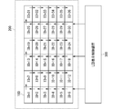
- FIG. 2 is a diagram illustrating a configuration of an LED display system according to Embodiment 1.
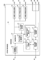
- FIG. 2 is a block diagram showing an internal configuration of one LED display device according to the first embodiment.
- FIG. 3 is a diagram illustrating a configuration of a first display unit according to the first embodiment.
- FIG. 3 is a diagram illustrating a configuration of a second display unit according to the first embodiment.
- FIG. 2 is a block diagram illustrating an internal configuration of the LED display control device according to the first embodiment.
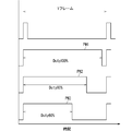
- FIG. 5 is a diagram illustrating an example of a duty ratio of a pulse width in PWM control according to the first embodiment.
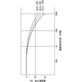
- FIG. 5 is a diagram illustrating an example of a luminance reduction characteristic for each duty ratio in the first embodiment.
- FIG. 15 is a diagram illustrating an example of a luminance reduction characteristic in a normal luminance mode and a high luminance mode in Embodiment 2.
- FIG. FIG. 15 is a diagram illustrating an example of a luminance reduction characteristic when a luminance mode is switched in the second embodiment.
- FIG. 13 is a block diagram showing an internal configuration of one LED display device according to Embodiment 3.
- FIG. 13 is a block diagram illustrating an internal configuration of an LED display control device according to a third embodiment.
- FIG. 14 is a diagram illustrating an example of a processing circuit in Embodiment 3.
- FIG. 21 is a diagram illustrating another example of the processing circuit in Embodiment 3.
- FIG. 1 is a diagram showing a configuration of the LED display system according to the first embodiment.
- the LED display system has a plurality of LED display devices 100 and an LED display control device 300.
- the plurality of LED display devices 100 constitute all the LED display devices 200 arranged in a matrix.
- the entire LED display device 200 is an array in which a plurality of LED display devices 100 are arranged.
- the all-LED display device 200 has one screen in which the display surfaces of the plurality of LED display devices 100 are arranged.
- the total LED display device 200 has a configuration in which six LED display devices 100 are arranged in the horizontal direction and six LED display devices 100 are arranged in the vertical direction.
- Each LED display device 100 has 320 horizontal pixels ⁇ 180 vertical pixels. Therefore, the entire LED display device 200 has one screen of Full @ HD consisting of 1920 ⁇ 1080 pixels.
- the LED display system can display an image including characters, graphics, images, and the like on one screen of all the LED display devices 200.
- the LED display control device 300 distributes a video signal to each LED display device 100, and displays a video on one screen of all the LED display devices 200 by communicating a control signal with each LED display device 100. Is performed.
- all the LED display devices 200 are divided into three groups. Each group includes twelve LED displays 100. The twelve LED display devices 100 in each group are daisy-chain connected to the LED display control device 300.
- the LED display control device 300 can efficiently perform video signal distribution and control signal communication by daisy chain connection.
- the LED display control device 300 is, for example, an LED control unit.
- FIG. 2 is a block diagram showing an internal configuration of one LED display device 100 according to the first embodiment.
- the LED display device 100 includes a first display unit 1, a second display unit 3, a video signal processing unit 6, a first drive unit 2, a communication unit 7, a second drive unit 4, a luminance measurement unit 5, a microcomputer circuit 8, and It has a memory circuit 9.
- FIG. 2 shows a video input terminal 11 and a control signal terminal 12 as components related to the LED display device 100.
- the first display unit 1 has a plurality of first LEDs provided on the display surface.
- the first display unit 1 has a plurality of pixels arranged in a matrix.
- the first display unit 1 forms a part of one screen of the entire LED display device 200.
- FIG. 3 is a diagram illustrating a configuration of the first display unit 1 according to the first embodiment.
- the first display unit 1 has a configuration in which 320 pixels 10 are arranged in the horizontal direction and 180 pixels 10 are arranged in the vertical direction.
- one pixel 10 has a configuration in which three first LEDs 1A respectively emitting red (R), green (G), and blue (B) emit light.
- the second display unit 3 has at least one second LED provided on a surface different from the display surface.
- the surface different from the display surface is, for example, a back surface located on the opposite side to the display surface.
- FIG. 4 is a diagram illustrating a configuration of the second display unit 3 according to the first embodiment.
- the second display unit 3 has a configuration in which two pixels 10 are arranged in the horizontal direction and two pixels 10 are arranged in the vertical direction.
- One pixel 10 in the second display unit 3 includes three second LEDs 3A that emit light in red (R), green (G), and blue (B) as one set.
- the second display unit 3 performs display for the LED display system to predict a change in luminance of the first display unit 1.
- each first LED 1A of the second display unit 3 when each second LED 3A of the second display unit 3 is driven under the same driving conditions (for example, the same driving current value) and for the same time as each first LED 1A of the first display unit 1, each first LED 1A indicates.
- the transition of the luminance and the transition of the equivalent luminance are shown.
- the luminance reduction rate of each second LED 3A is the same as or similar to the luminance reduction rate of each first LED 1A.
- Each first LED 1A and each second LED 3A are, for example, LEDs of the same production lot. LEDs having the same production lot have similar characteristics such as brightness and wavelength. When both are driven by the same drive current, the respective luminance reduction rates are equal.
- the video input terminal 11 receives a video signal from the preceding LED display device 100 or LED display control device 300 connected in a daisy chain.
- the video signal is a signal including video data of a video to be displayed on all LED display devices 200.
- the video signal processing unit 6 performs a process such as a selection process on the video signal received at the video input terminal 11. In the selection process, the video signal processing unit 6 selects a video area to be displayed by the LED display device 100 including itself from the video included in the video signal.
- the first drive section 2 drives each first LED 1A under the first drive condition based on the video signal.
- the first driving condition includes a condition relating to a duty ratio for performing PWM control on each first LED 1A.
- the first driver 2 performs PWM control and drives each of the first LEDs 1A for each color based on the signal processed by the video signal processor 6.
- the first display unit 1 displays an image in the image area selected by the image signal processing unit 6.
- the control signal terminal 12 receives a control signal from the preceding LED display device 100 or LED display control device 300 connected in a daisy chain.
- the control signal is, for example, a signal including control data such as a luminance correction coefficient.
- the communication unit 7 communicates with the LED display control device 300 via the control signal terminal 12 or the like.
- the communication unit 7 outputs a control signal received from the LED display control device 300 to the microcomputer circuit 8.
- the communication unit 7 transmits a control signal input from the microcomputer circuit 8 to the LED display control device 300.
- the second driving unit 4 drives each of the second LEDs 3A under one of a plurality of predetermined second driving conditions.
- the second driving condition includes a condition relating to a duty ratio for performing PWM control of each second LED 3A.
- the second driver 4 performs PWM control and drives each second LED 3A at one of three predetermined duty ratios.
- the second drive unit 4 drives each second LED 3A under different second drive conditions for each of the three groups into which the plurality of LED display devices 100 are divided.
- the second LED 3A in each of the LED display devices 100 having IDs of 13 to 24 is driven at a duty ratio of 80%.
- the second LED 3A in each of the LED display devices 100 having IDs of 25 to 36 is driven at a duty ratio of 60%.
- the second driving section 4 always drives each second LED 3A under one second driving condition.
- the luminance measuring unit 5 measures the luminance of at least one second LED 3A.
- the luminance measuring unit 5 includes, for example, a light receiving element.
- the measurement result of the luminance is output to the microcomputer circuit 8.
- the microcomputer circuit 8 controls the components of the LED display device 100 as a whole.
- the microcomputer circuit 8 controls the video signal processing unit 6, controls the drive unit, controls the communication unit 7, controls the second drive unit 4, controls the luminance measurement unit 5, and sends the control signal to the memory circuit 9. Control of reading and writing.
- the memory circuit 9 stores various parameters.
- the various parameters include, for example, an individual luminance correction coefficient that is a coefficient for correcting the luminance of each first LED 1A, a corrected luminance that is the luminance of each first LED 1A corrected by the individual luminance correction coefficient, and other necessary setting values and adjustments. Contains the value.
- the individual luminance correction coefficient is a luminance correction coefficient obtained individually for each LED display device 100, and is a luminance correction coefficient for correcting luminance variation and chromaticity variation in each LED display device 100.
- the memory circuit 9 stores the initial value of the individual luminance correction coefficient and the initial value of the corrected luminance at the time of shipment from the factory.
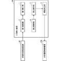
- FIG. 5 is a block diagram showing an internal configuration of the LED display control device 300 according to the first embodiment.
- the LED display control device 300 includes a video signal processing circuit 30, a control circuit 20, and a video division transfer circuit 40.
- FIG. 5 shows a video signal input terminal 50, an external signal terminal 60, a video output terminal 70, and a control signal terminal 80 as components related to the LED display control device 300.
- the video signal input terminal 50 receives a video signal from the outside.
- the video signal processing circuit 30 performs processing such as gamma correction on the video signal received at the video signal input terminal 50.
- the external signal terminal 60 receives a control signal for controlling the LED display control device 300 and each LED display device 100 from an external PC (Personal Computer) or the like.
- the control circuit 20 transmits a control signal to the plurality of LED display devices 100 and receives a control signal from the plurality of LED display devices 100. Thereby, the control circuit 20 controls all the LED display devices 200. Further, the control circuit 20 controls the correction of the video signal based on the control signal received at the external signal terminal 60 and the control signal transmitted from each communication unit 7 of the plurality of LED display devices 100.
- the video division transfer circuit 40 divides the video signal corrected by the control circuit 20 into three video signals corresponding to the video to be displayed by the LED display devices 100 belonging to each group.
- the video division transfer circuit 40 transmits three video signals to the three groups of LED display devices 100, respectively.
- the control circuit 20 includes a lighting time calculation unit 24, a parameter storage unit 25, a brightness reduction characteristic calculation unit 21, a brightness correction unit 22, an external communication control unit 26, and an internal communication control unit 27. Further, the brightness correction unit 22 includes a correction coefficient calculation unit 23.
- the lighting time calculation unit 24 calculates and stores the cumulative lighting time and the average duty ratio of each first LED 1A in 1920 ⁇ 1080 pixels of all the LED display devices 200 at regular intervals.
- the internal communication control unit 27 stores parameters included in the control signal received at the control signal terminal 80 in the parameter storage unit 25, and outputs the parameters to the external communication control unit 26, the brightness correction unit 22, or the brightness reduction characteristic calculation unit 21. Or Further, the internal communication control unit 27 transmits the parameters stored in the parameter storage unit 25 to the plurality of LED display devices 100 via the control signal terminals 80. Alternatively, the internal communication control unit 27 transmits parameters and the like input from the external communication control unit 26, the brightness correction unit 22, or the brightness reduction characteristic calculation unit 21 to the plurality of LED display devices 100 via the control signal terminal 80. .
- the luminance lowering characteristic calculation unit 21 acquires, from the plurality of LED display devices 100, the measurement results of the luminance of the second LEDs 3A driven under different second driving conditions.
- the brightness reduction characteristic calculation unit 21 calculates the brightness reduction characteristics with respect to the cumulative lighting time of the second LED 3A for each of a plurality of predetermined second driving conditions, and acquires a plurality of brightness reduction characteristics.
- the luminance correction unit 22 corrects the luminance of the video signal processed by the video signal processing circuit 30.
- the brightness correction unit 22 corrects the brightness of the video signal for each of the plurality of first LEDs 1A based on one of the plurality of brightness reduction characteristics and the cumulative lighting time of each first LED 1A.
- the brightness correction unit 22 selects, for example, one brightness reduction characteristic based on the first driving condition. That is, the brightness correction unit 22 selects a brightness reduction characteristic driven at a duty ratio close to the average duty ratio of the first LED 1A.
- the correction coefficient calculator 23 calculates a first luminance correction coefficient for uniformly correcting the luminance on one screen of the entire LED display device 200. At this time, the correction coefficient calculation unit 23 calculates the first luminance correction coefficient based on the individual luminance correction coefficient in each LED display device 100. For example, the correction coefficient calculation unit 23 calculates the first luminance correction coefficient based on the individual luminance correction coefficient and the corrected luminance obtained from the plurality of LED display devices 100 so that the luminance on one screen is uniform. Further, the correction coefficient calculator 23 calculates a second luminance correction coefficient obtained by correcting the first luminance correction coefficient based on the cumulative lighting time of each first LED 1A in one luminance reduction characteristic. The brightness correction unit 22 corrects the brightness of the video included in the video signal for each of the first LEDs 1A using the second brightness correction coefficient.
- the external communication control unit 26 stores parameters included in the control signal received at the external control terminal in the parameter storage unit 25 or outputs the parameters to the internal communication control unit 27. Further, the external communication control unit 26 transmits the parameters stored in the parameter storage unit 25 or the parameters input from the internal communication control unit 27 to the outside via the external control terminal.
- the memory circuit 9 stores the individual brightness correction coefficient and the initial value of the corrected brightness at the time of shipment from the factory.
- the method for obtaining the individual luminance correction coefficient and the corrected luminance will be described below.
- the individual luminance correction coefficient and the corrected luminance are obtained, for example, by measuring the luminance of each first LED 1A corresponding to each of R, G, and B in each pixel 10.
- Equation (1) shows the individual luminance correction coefficients Cr (uh, uv), Cg (uh, uv), and Cb (uh, uv).
- Yr (uh, uv), Yg (uh, uv), and Yb (uh, uv) are R luminance, G luminance, and B luminance of the first LED 1A before correction, respectively.
- Yr (uh, uv), Yg (uh, uv), and Yb (uh, uv) indicate that all the first LEDs 1A in one LED display device 100 are lit at the maximum gradation.
- Yr_min, Yg_min, and Yb_min correspond to the minimum luminance of Yr (uh, uv), Yg (uh, uv), and Yb (uh, uv).
- the luminances (corrected luminances) of R, G, and B of each first LED 1A corrected by the individual luminance correction coefficient are equal to Yr_min, Yg_min, and Yb_min, respectively. That is, the brightness of the display surface of each LED display device 100 is made uniform by lowering the brightness of the first LED 1A, which is higher than the minimum brightness.
- the memory circuit 9 stores the individual luminance correction coefficients Cr (uh, uv), Cg (uh, uv), Cb (uh, uv) and the correction luminances Yr_min, Yg_min, Yb_min. Under the control of the microcomputer circuit 8, the communication unit 7 transmits the individual brightness correction coefficient and the brightness correction stored in the memory circuit 9 to the LED display control device 300.
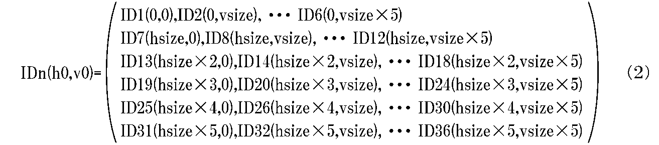
- the LED display control device 300 associates the ID number of each LED display device 100 with the coordinate position of the pixel 10 on the entire 1920 ⁇ 1080 pixel screen.
- the following equation (2) indicates the coordinates IDn (h0, v0) of the pixel 10 located at the upper left of each LED display device 100.
- n is an ID number.
- the LED display control device 300 acquires the individual luminance correction coefficient and the corrected luminance from each LED display device 100.
- the correction coefficient calculation unit 23 obtains a first luminance correction coefficient of the entire screen composed of 1920 ⁇ 1080 pixels based on the individual luminance correction coefficient and the corrected luminance. More specifically, the correction coefficient calculation unit 23 obtains a first luminance correction coefficient by multiplying the individual luminance correction coefficient by a correction coefficient obtained from the corrected luminance.
- the first luminance correction coefficients Cr0 (h, v), Cg0 (h, v), Cb0 (h, v) in each LED display device 100 are expressed by the following equations (3) to (9).
- Expressions (3) to (9) are expressions for obtaining the first luminance correction coefficient of the LED display device 100 corresponding to the representative ID.
- the first luminance correction coefficient of the LED display device 100 corresponding to an ID not shown in each of the following equations can be similarly obtained.
- IDn_Cr (uh, uv), IDn_Cg (uh, uv), and IDn_Cb (uh, uv) are individual brightness correction coefficients of each LED display device 100 received by the LED display control device 300.
- IDnYr_min, IDnYg_min, and IDnYb_min are correction luminances of the respective LED display devices 100 received by the LED display control device 300.
- Unit_Yr_min, Unit_Yg_min, and Unit_Yb_min are the minimum values of the corrected luminance in all the LED display devices 200.
- Unit_Yr_min / IDn_Yr_min, Unit_Yg_min / IDn_Yg_min, Unit_Yb_min / IDn_Yb_min correspond to the above-described correction coefficients.
- the correction coefficient calculator 23 calculates the first luminance correction coefficient by multiplying the individual luminance correction coefficient by the correction coefficient, as shown in the above equations.
- the parameter storage unit 25 stores the calculated first luminance correction coefficients.
- the brightness of the display surface of each LED display device 100 can already be made uniform by the individual brightness correction coefficient.
- the brightness correction unit 22 can further equalize the brightness of one screen of all the LED display devices 200 using the first brightness correction coefficient. As shown in the above equations, the brightness correction unit 22 can set the minimum brightness value on one screen of the entire LED display device 200 as a reference value of the brightness of the entire LED display device 200.
- the LED display control device 300 can reduce the variation in brightness and the variation in chromaticity among the plurality of LED display devices 100 by using the first brightness correction coefficient.
- the luminance correction unit 22 corrects the luminance of each first LED 1A with the second luminance correction coefficient obtained by correcting the first luminance correction coefficient, for further reducing the luminance variation.
- the second luminance correction coefficient is a luminance correction in which the first luminance correction coefficient is corrected based on the cumulative lighting time of all the LED display devices 200 and the luminance measurement result of the second display unit 3 in each LED display device 100. It is a coefficient.
- FIG. 6 is a diagram illustrating an example of the duty ratio of the pulse width in the PWM control.
- FIG. 6 shows, from the top, a basic cycle, a waveform PW1 having a duty ratio of 100%, a waveform PW2 having a duty ratio of 80%, and a waveform PW3 having a duty ratio of 60%.
- the basic period of the PWM is equal to or shorter than one frame period of the video signal.
- the first drive unit 2 changes the duty ratio based on the luminance information included in the video signal, that is, changes the lighting period and the light-off period of each first LED 1A per unit time.
- the first drive unit 2 can adjust the luminance for each color recognized by human eyes by changing the duty ratio for each color.
- the first driving unit 2 drives each first LED 1A at a duty ratio corresponding to the brightness corrected for each first LED 1A. That is, the lighting period and the light-off period per unit time are changed. As a result, each first LED 1A lights up with the corrected luminance.
- the LED display system performs the display operation of the first display unit 1, that is, the drive, and the display operation of the second display unit 3, that is, the drive in parallel.
- Each of the first LED 1A and each of the second LEDs 3A in one LED display device 100 are lit in a similar environment, and the luminance reduction rates of the two approach each other.
- the cumulative lighting time of both is different. Since the lighting of the plurality of first LEDs 1A is controlled based on the image displayed on the first display unit 1, there are many times when the first LEDs 1A are not turned on. On the other hand, the lighting of each second LED 3A is not always based on the image displayed on the first display unit 1, but is always controlled at one of a plurality of predetermined duty ratios. That is, each second LED 3A is always lit at a constant duty ratio. Further, since the lighting of the plurality of first LEDs 1A is controlled based on the brightness of the image, the accumulated lighting time differs for each pixel 10. That is, there is a difference in the cumulative lighting time of each first LED 1A.
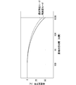
- FIG. 7 is a diagram illustrating an example of a luminance reduction characteristic for each duty ratio in the first embodiment.
- the brightness lowering characteristic is a relationship between the cumulative lighting time and the brightness lowering rate.
- FIG. 7 shows the luminance reduction rates when the second LED 3A is turned on at duty ratios of 100%, 80%, and 60%, respectively. Note that a logarithmic scale is applied to the scale of the cumulative lighting time in FIG. The higher the duty ratio is, the higher the brightness of the second LED 3A is. Therefore, the heat load accompanying the temperature rise due to light emission is large. As a result, the luminance reduction rate of the second LED 3A increases. Further, the lower the duty ratio, the smaller the temperature rise due to the light emission of the second LED 3A. Since the decrease in luminance due to the temperature rise can be ignored, the variation in the luminance decrease rate depending on the change in the duty ratio is reduced.
- the second LED 3A and the first LED 1A have similar luminance reduction characteristics. Therefore, the brightness of the first LED 1A also decreases in accordance with the cumulative lighting time, similarly to the brightness reduction characteristics shown in FIG.
- the LED display system according to Embodiment 1 corrects the luminance of each first LED 1A based on the cumulative lighting time of each first LED 1A.
- a luminance correction operation after luminance correction at the time of initial installation will be described in detail.
- the LED display system controls the driving of the second LED 3A as described below.
- ID 25.
- the second LEDs 3A in the to 36 LED display devices 100 are driven at a duty ratio of 60%.
- the luminance measurement result of the second LED 3A measured by the luminance measuring unit 5 is input to the microcomputer circuit 8.
- the microcomputer circuit 8 calculates the luminance reduction rate of the second LED 3A from the initial value of the luminance measurement result of the second LED 3A and the current luminance measurement result. In each of the plurality of LED display devices 100, the luminance reduction rate of the second LED 3A is calculated.
- the brightness reduction characteristic calculation unit 21 obtains the brightness reduction rate of the second LED 3A from each LED display device 100 via the communication unit 7. That is, the brightness reduction characteristic calculation unit acquires a plurality of brightness reduction rates corresponding to the second LEDs 3A, each of which is driven at a different duty ratio.
- the brightness reduction characteristic calculation unit 21 generates a brightness reduction rate table based on the energization time of each LED display device 100 and the brightness reduction rate. At this time, the brightness reduction characteristic calculation unit 21 generates a brightness reduction rate table for each duty ratio.
- the parameter storage unit 25 stores the generated luminance reduction rate table.
- the brightness reduction characteristic calculation unit 21 updates the brightness reduction rate table as time elapses, and the parameter storage unit 25 stores the updated brightness reduction rate table.
- the brightness reduction characteristic calculation unit 21 receives the brightness reduction rate from each LED display device 100 every hour and updates the brightness reduction rate table.
- the brightness reduction characteristic calculation unit 21 calculates the average value of the 12 brightness reduction rates obtained from the 12 LED display devices 100, and generates a brightness reduction rate table for each duty ratio.
- the lighting time calculation unit 24 calculates the average duty ratio, the cumulative lighting time (Tr, Tg, Tb) and the cumulative energizing time of the LED display device 100 for each of the first LEDs 1A in all the LED display devices 200 by a certain unit time. Remember each time.
- the lighting time calculator 24 calculates the average duty ratio and the cumulative lighting time based on the output of the brightness corrector 22. For example, if the unit energization time is one hour and the duty ratio in the unit energization time is 10% (that is, the brightness level is 10%), the lighting time calculation unit 24 sets the lighting time calculation unit 24 to 0.1 hours every one hour. The lighting time is added to the cumulative lighting time. In addition, the lighting time calculation unit 24 calculates the average duty ratio by dividing the cumulative lighting time of each first LED 1A by the cumulative energizing time of the LED display device 100.
- the correction coefficient calculating unit 23 obtains the luminance maintaining ratio of all the LED display devices 200 based on the cumulative lighting time calculated by the lighting time calculating unit 24 and the luminance reduction rate table stored in the parameter storage unit 25. At this time, the correction coefficient calculation unit 23 obtains a luminance maintenance ratio for each color.
- the R luminance maintenance ratio Pr (h, v) of each pixel 10 is obtained by the following equation (10) from equation (12).
- the G luminance maintenance ratio Pg (h, v) of each pixel 10 is obtained by the following expression (13) from expression (15).
- the B luminance maintenance ratio Pb (h, v) of each pixel 10 is obtained from the following equations (16) to (18).
- FPr1 (t), FPg1 (t), and FPb1 (t) are R luminance maintenance ratio per cumulative lighting time at a duty ratio of 100% obtained from the luminance measurement result of each second display unit 3, and G The luminance maintenance ratio and the B luminance maintenance ratio.
- FPr2 (t), FPg2 (t), and FPb2 (t) are an R luminance maintenance rate, a G luminance maintenance rate, and a B luminance maintenance rate at a duty ratio of 80%, respectively.
- FPr3 (t), FPg3 (t), and FPb3 (t) are an R luminance maintenance ratio, a G luminance maintenance ratio, and a B luminance maintenance ratio at a duty ratio of 60%, respectively.
- Tr (h, v), Tg (h, v), Tb (h, v) are cumulative lighting times of the first LED 1A for each color.
- Dr (h, v), Dg (h, v), Db (h, v) are the average duty ratios of the first LED 1A for each color.
- h is a horizontal pixel position (0 to 1919)
- v is a vertical pixel position (0 to 1079).
- Equation (10) shows the R luminance maintenance ratio Pr (h, v) when Dr (h, v)> 80%.
- Equation (11) shows the R luminance maintenance ratio Pr (h, v) when 80% ⁇ Dr (h, v)> 60%.
- Equation (12) shows the R luminance maintenance ratio Pr (h, v) when 60% ⁇ Dr (h, v).
- Equation (13) shows the G luminance maintenance ratio Pg (h, v) when Dg (h, v)> 80%.
- Equation (14) shows the G luminance maintenance ratio Pg (h, v) when 80% ⁇ Dg (h, v)> 60%.
- Equation (15) shows the G luminance maintenance ratio Pg (h, v) when 60% ⁇ Dg (h, v).
- Equation (16) shows the B luminance maintenance ratio Pb (h, v) when Db (h, v)> 80%.
- Equation (17) shows the B luminance maintenance ratio Pb (h, v) when 80% ⁇ Db (h, v)> 60%.
- Equation (18) shows the B luminance maintenance ratio Pb (h, v) when 60% ⁇ Db (h, v).
- the LED display system uses the first luminance correction coefficients Cr0 (h, v), Cg0 (h, v), and Cb0 (h, v). Perform brightness correction.
- the relative value of the actual luminance in consideration of the luminance maintenance rate is expressed by the following equation (19).
- the correction coefficient calculator 23 calculates the relative values Qr (h, v), Qg (h, v), and Qb (h, v) of the actual luminance using the above equation (19). Then, the correction coefficient calculation unit 23 obtains the minimum value Qrgb_min of the relative value of the actual luminance in all the R, G, and B pixels. Further, the correction coefficient calculator 23 calculates the second luminance correction coefficients Cr1 (h, v), Cg1 (h, v), Cb1 for correcting the initial luminance variation of the first LED 1A and the luminance decrease due to the cumulative lighting time. (H, v) is obtained using the following equation (20).
- the correction coefficient calculation unit 23 obtains the luminance maintaining ratio of each of the plurality of first LEDs 1A of one LED display device 100 based on the cumulative lighting time of one LED display device 100. At this time, the correction coefficient calculation unit 23 obtains a luminance maintenance ratio for each color of the first LED 1A. Similarly, the correction coefficient calculating unit 23 calculates the other lighting time based on the accumulated lighting time and the average duty ratio (average brightness) of the other LED display devices 100 and the brightness reduction rate table actually measured by each LED display device 100. The brightness maintenance ratio of each color of each of the plurality of first LEDs 1A of the LED display device 100 is obtained.
- the correction coefficient calculation unit 23 calculates the first luminance correction coefficients Cr0 (h, v), Cg0 (h, v), Cb0 (h, v) by using the luminance maintenance ratio of one LED display device 100 and another luminance maintenance factor. Based on the luminance maintaining ratio of the LED display device 100, the luminance is changed to the second luminance correction coefficient Cr1 (h, v), Cg1 (h, v), Cb1 (h, v).
- the brightness correction unit 22 corrects the brightness of the video data included in the video signal based on the second brightness correction coefficient.
- the correction coefficient calculation unit 23 calculates the second luminance correction coefficients Cr1 (h, v), Cg1 (h, v), and Cb1 (h, v) and corrects the luminance at regular time intervals (for example, 100 hours). May be implemented. Alternatively, the correction coefficient calculation unit 23 may perform the calculation and the brightness correction when a brightness drop occurs. The occurrence of the luminance decrease is, for example, a case where Qrgb_min is reduced by 10% or more from Qrgb_min at the time of the previous correction.
- the duty ratio for driving each second LED 3A for each of the three groups is set to three types of 100%, 80%, and 60%, but is not limited thereto. The duty ratio may be any two or more duty ratios.
- each first LED 1A is not necessarily driven at a duty ratio of 100%.
- the LED display system cannot accurately predict the luminance reduction rate in the first display unit 1. As a result, the prediction error of the luminance decrease becomes large, and the luminance uniformity accuracy of the screen after correction deteriorates.
- each second LED 3A is driven at a plurality of duty ratios for each of the plurality of LED display devices 100.
- the LED display system selects and corrects the luminance reduction rate table having the most appropriate duty ratio from the average luminance of each pixel 10. As a result, the prediction error of the luminance decrease is reduced, and the luminance uniformity accuracy after the correction is improved.
- the luminance correction unit 22 can also correct the luminance by using a luminance reduction rate table stored in the parameter storage unit 25 before shipment from the factory.
- the decrease in the brightness of the first LED 1A changes depending on the environmental temperature and the like.
- the accuracy of brightness correction is improved by providing the second display unit 3 for brightness measurement in each LED display device 100.
- each of the plurality of second LEDs 3A is driven at a different duty ratio in one LED display device 100, similarly, a luminance reduction rate table for each duty ratio can be obtained.
- the brightness measurement sequence of each second LED 3A is complicated.
- the second LED 3A in the first embodiment is driven at one duty ratio in one LED display device 100.
- the LED display control device 300 collects the brightness measurement results of the second LEDs 3A driven at different duty ratios from the plurality of LED display devices 100, and calculates a plurality of brightness reduction characteristics. Therefore, the luminance measurement sequence in one LED display device 100 can be simplified.
- the LED display system includes a plurality of LED display devices 100 that are arranged in a matrix and have one screen in which display surfaces of the LED display devices are arranged.
- An LED display control device 300 that distributes a video signal to each and controls to display a video on one screen.
- Each of the plurality of LED display devices 100 includes a first display unit 1 including a plurality of first LEDs 1A provided on a display surface, and a second display unit 3 including at least one second LED 3A provided on a surface different from the display surface.
- a luminance measuring unit 5 that measures the luminance of at least one second LED 3A, a first driving unit 2 that drives each of the plurality of first LEDs 1A under a first driving condition based on a video signal, and a plurality of predetermined second LEDs 3A.
- a second driving unit 4 that drives at least one second LED 3A under one of the two driving conditions.
- the LED display control device 300 acquires, from the plurality of LED display devices 100, the measurement results of the luminance of at least one second LED 3A that is driven under different second driving conditions, and obtains the luminance with respect to the cumulative lighting time of at least one second LED 3A.
- a brightness reduction characteristic calculating unit 21 that calculates the brightness reduction characteristics for each of a plurality of predetermined second driving conditions and obtains a plurality of brightness reduction characteristics; And a brightness correction unit 22 that corrects the brightness of the video included in the video signal for each of the plurality of first LEDs 1A based on the cumulative lighting time of each of the first LEDs 1A.
- the LED display control device 300 controls the display of the video after the brightness correction on one screen by distributing the video signal after the brightness correction to the plurality of LED display devices 100.
- the LED display system improves the uniformity of luminance and chromaticity of the first display unit 1 that displays an image or the like.
- the brightness correction unit 22 of the LED display system according to the first embodiment selects one of the plurality of brightness reduction characteristics based on the first driving condition.
- the uniformity of luminance and chromaticity of the first display unit 1 is improved with high accuracy.
- the first driving condition includes a condition relating to a duty ratio for performing PWM control on the plurality of first LEDs 1A.
- Each of the predetermined plurality of second drive conditions includes a condition relating to a duty ratio for performing PWM control on at least one second LED 3A.
- the LED display system accurately improves the uniformity of luminance and chromaticity caused by the duty ratio.
- the brightness correction unit 22 of the LED display system calculates a first brightness correction coefficient for uniformly correcting the brightness of each of the plurality of first LEDs 1A on one screen, and calculates one brightness reduction characteristic.
- a correction coefficient calculation unit configured to further calculate a second luminance correction coefficient obtained by correcting the first luminance correction coefficient based on the cumulative lighting time of each of the plurality of first LEDs;
- the brightness correction unit 22 corrects the brightness of the video included in the video signal for each of the first LEDs 1A using the second brightness correction coefficient.
- the LED display system improves the uniformity of the luminance and chromaticity of the first display unit 1.
- At least one second LED 3A of the LED display system according to Embodiment 1 has the same brightness lowering characteristics as the plurality of first LEDs 1A when driven under the same driving conditions and the same time as the plurality of first LEDs 1A. Have.
- the LED display system can accurately obtain the luminance reduction characteristic, and accurately improve the uniformity of the luminance and chromaticity of the first display unit 1.
- the first drive unit 2 of each LED display device 100 drives each first LED 1A with a fixed drive current.
- the LED display system according to Embodiment 2 corrects the luminance of all LED display devices 200 by changing the drive current of LED display device 100.
- the LED display system switches the drive current flowing through each first LED 1A between two types, a high brightness mode and a normal brightness mode.
- the drive current value in the high brightness mode is larger than the drive current value in the normal brightness mode.
- the operation is performed in the normal luminance mode, and the operation is switched to the high luminance mode as necessary in an emergency or the like.
- the LED display system switches the mode.
- the LED display system switches the above mode. The case where it is difficult for the observer to see is considered, for example, when the content displayed on the first display unit 1 is changed from dark to bright.
- the first drive unit 2 adjusts the brightness by simultaneously changing the drive current values of the plurality of first LEDs 1A. I do. In one luminance mode, the drive current values of the plurality of first LEDs 1A are the same.
- the LED display system needs to measure the brightness reduction rate of the second LED 3A in the high brightness mode and the brightness reduction rate of the second LED 3A in the normal brightness mode.
- the LED display system controls each LED display device 100 as described below.
- the brightness reduction characteristic calculation unit 21 obtains the brightness reduction rate of the second LED 3A from each LED display device 100 via the communication unit 7.
- the brightness reduction characteristic calculation unit 21 generates a brightness reduction rate table in the high brightness mode and in the normal brightness mode based on the energization time of each LED display device 100 and the brightness reduction rate. At this time, the brightness reduction characteristic calculation unit 21 generates a brightness reduction rate table for each duty ratio.
- the parameter storage unit 25 stores the generated luminance reduction rate table.
- the luminance reduction characteristic calculation unit 21 updates the luminance reduction ratio table for each duty ratio as time elapses. For example, the brightness reduction characteristic calculation unit 21 receives the brightness reduction rate from each LED display device 100 every hour and updates the brightness reduction rate table. There are six LED display devices 100 for one duty ratio.
- the brightness reduction characteristic calculation unit 21 calculates an average value of the six brightness reduction rates obtained from the six LED display devices 100, and generates a brightness reduction rate table.
- the correction coefficient calculator 23 calculates the brightness reduction rate of all the LED display devices 200 based on the cumulative lighting time calculated by the lighting time calculator 24 and the brightness reduction rate table stored in the parameter storage 25. At this time, the correction coefficient calculation unit 23 calculates a luminance reduction rate for each color.
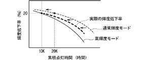
- FIG. 8 is a diagram illustrating an example of a luminance reduction characteristic in the normal luminance mode and the high luminance mode according to the second embodiment.
- the luminance reduction rate of the second LED 3A increases.
- the drive current value in the high brightness mode is larger than the drive current value in the normal brightness mode. Therefore, the heat load accompanying the temperature rise is large.
- the brightness reduction rate of the second LED 3A that is lit in the high brightness mode is greater than that of the second LED 3A that is lit in the normal brightness mode.
- each first LED 1A of the first display unit 1 has a similar brightness reduction characteristic to the extent that the brightness reduction rate of each second LED 3A can be identified.
- each first LED 1A decreases with the cumulative lighting time.
- the luminance correction unit 22 corrects the luminance of the first LED 1A based on the luminance reduction rate of the normal luminance mode in which the same cumulative lighting time has simply elapsed at the time of the transition. Get different correction results. That is, the luminance correction unit 22 cannot accurately correct the luminance.
- the LED display system according to Embodiment 2 converts the cumulative lighting time in the high brightness mode immediately before changing the brightness mode into the corresponding cumulative lighting time in the normal brightness mode. With this conversion, the LED display system can accurately predict the luminance reduction rate of the first LED 1A, and thus can reduce the luminance variation and the chromaticity variation of the first display unit 1.
- FIG. 9 is a diagram illustrating an example of a luminance reduction characteristic when the luminance mode is switched according to the second embodiment. Note that FIG. 9 shows, as an example, only each luminance reduction rate of the cumulative lighting time with respect to a duty ratio of 100%.
- the correction coefficient calculation unit 23 calculates the cumulative lighting time T1 indicating the luminance reduction rate of 20% in the graph indicating the luminance reduction rate in the normal luminance mode. That is, the correction coefficient calculation unit 23 calculates the cumulative lighting time in the normal brightness mode in which the brightness reduction rate corresponding to the brightness reduction rate in the high brightness mode is obtained.
- the first LED 1A when the first LED 1A is turned on for 10K hours in the high brightness mode and then for 100 hours in the normal brightness mode, the first LED 1A shows the brightness reduction rate when turned on for 20K hours +100 hours only in the normal brightness mode.
- the correction coefficient calculation unit 23 obtains a second luminance correction coefficient using the luminance reduction rate when turned on for 20 K hours + 100 hours in the normal luminance mode.
- the R luminance maintenance ratio Pr (h, v) is expressed by the following equations (21) to (23).
- FPrh1 (t) is the R luminance maintenance rate per cumulative lighting time in the high luminance mode and at a duty ratio of 100%.
- FPrn1 (t) is the R luminance maintenance rate per cumulative lighting time in the normal luminance mode and at a duty ratio of 100%.
- Prh (h, v) is the R luminance maintenance ratio for each pixel 10 in the high luminance mode.
- Prn (h, v) is the R luminance maintenance ratio in the normal luminance mode.
- t0 is the cumulative lighting time in the high brightness mode.
- Equation (22) shows the R luminance maintenance ratio (h, v) in the normal luminance mode when switching from the high luminance mode to the normal luminance mode.
- the correction coefficient calculation unit 23 calculates T1 that satisfies Expression (22).
- Equation (23) shows the R luminance maintenance ratio (h, v) after switching to the normal luminance mode.
- t1 is the cumulative lighting time after switching to the normal luminance mode.
- the brightness mode for driving the second LED 3A of the second display unit 3 is not limited to two types of brightness modes such as a high brightness mode and a normal brightness mode.
- the LED display system may drive each of the second LEDs 3A of the plurality of LED display devices 100 in three or more types of brightness modes.
- the LED display system according to Embodiment 2 converts the cumulative lighting time before changing the brightness mode into the cumulative lighting time after changing the brightness mode when changing the brightness mode. Accordingly, the LED display system can accurately predict the luminance maintenance ratio of the first LED 1A, and thus can reduce the luminance variation and the chromaticity variation of the first display unit 1.
- the luminance correction unit 22 can also correct the luminance by using a luminance reduction rate table stored in the parameter storage unit 25 before shipment from the factory.
- the decrease in the brightness of the first LED 1A changes depending on the environmental temperature and the like.
- the accuracy of brightness correction is improved by providing the second display unit 3 for brightness measurement in each LED display device 100.
- each of the plurality of second LEDs 3A is driven in a different brightness mode (drive current value) and a different duty ratio in one LED display device 100, similarly, a brightness reduction rate table for each brightness mode and each duty ratio Is obtained.
- the brightness measurement sequence of each second LED 3A is complicated.
- the second LED 3A in the second embodiment is driven in one LED display device 100 in one luminance mode (one drive current value) and duty ratio.
- the LED display control device 300 collects the brightness measurement results of the second LEDs 3A driven at different duty ratios from the plurality of LED display devices 100, and calculates a plurality of brightness reduction characteristics. Therefore, the luminance measurement sequence in one LED display device 100 can be simplified.
- the first driving condition in the LED display system according to Embodiment 3 includes a condition relating to a driving current for driving the plurality of first LEDs 1A.
- Each of the predetermined plurality of second driving conditions includes a condition relating to a driving current for driving at least one second LED 3A.
- the LED display system can accurately improve the uniformity of luminance and chromaticity even when the luminance of the first display unit 1 is adjusted by changing the drive current of the first LED 1A during operation. I do.
- the LED display system according to the third embodiment is a superordinate concept of the LED display system according to the first or second embodiment. That is, the LED display system according to the first or second embodiment includes the components of the LED display system according to the third embodiment. The description of the same configuration and operation as those of the first or second embodiment is omitted.
- FIG. 10 is a block diagram showing an internal configuration of one LED display device 100 according to the third embodiment.
- the LED display device 100 includes a first display unit 1, a first drive unit 2, a second display unit 3, a second drive unit 4, and a luminance measurement unit 5.
- the first display unit 1 includes a plurality of first LEDs provided on the display surface.
- the first driving unit 2 drives each of the plurality of first LEDs under a first driving condition based on a video signal.
- the video signal is input from, for example, an LED display control device 301 described later via the video division transfer circuit 40.
- the second display unit 3 includes at least one second LED provided on a surface different from the display surface.
- the second drive unit 4 drives at least one second LED under one of a plurality of predetermined second drive conditions.
- the luminance measuring unit 5 measures the luminance of at least one second LED.
- the luminance measurement unit 5 outputs the measurement result to the LED display control device 301 via the internal communication control device 27A, for example.
- the configuration and functions of internal communication control device 27A are the same as those of internal communication control unit 27 in the first embodiment.
- FIG. 11 is a block diagram showing an internal configuration of the LED display control device 301 according to the third embodiment.
- the LED display control device 301 includes a luminance reduction characteristic calculation unit 21 and a luminance correction unit 22.
- the luminance reduction characteristic calculation unit 21 acquires, from the plurality of LED display devices 100, the measurement results of the luminance of at least one second LED that is driven under different second driving conditions.
- the brightness reduction characteristic calculation unit 21 acquires, for example, a brightness measurement result via the internal communication control device 27A.
- the brightness reduction characteristic calculation unit 21 calculates the brightness reduction characteristics for the cumulative lighting time of each of the at least one second LED for each of a plurality of predetermined second driving conditions, and acquires a plurality of brightness reduction characteristics.
- the brightness correction unit 22 corrects the brightness of the video included in the video signal for each of the plurality of first LEDs based on one of the plurality of brightness reduction characteristics and the cumulative lighting time of each of the plurality of first LEDs. I do.
- the LED display control device 301 controls the display of the video after the luminance correction on one screen by distributing the video signal after the luminance correction to each of the first driving units 2 of the plurality of LED display devices 100.
- the LED display control device 301 distributes, for example, the video signal after the luminance correction to each of the first driving units 2 via the video division transfer circuit 40.
- the video signal before the luminance correction is input from the video signal processing circuit 30, for example.
- FIG. 12 is a diagram illustrating an example of the processing circuit 90 included in the LED display control device 301.
- Each function of the brightness reduction characteristic calculation unit 21 and the brightness correction unit 22 is realized by the processing circuit 90. That is, the processing circuit 90 includes the luminance reduction characteristic calculation unit 21 and the luminance correction unit 22.
- the processing circuit 90 When the processing circuit 90 is dedicated hardware, the processing circuit 90 includes, for example, a single circuit, a composite circuit, a programmed processor, a parallel programmed processor, an ASIC (Application Specific Integrated Circuit), and an FPGA (Field-Programmable). Gate Array) or a circuit combining these.
- Each function of the brightness reduction characteristic calculation unit 21 and the brightness correction unit 22 may be individually realized by a plurality of processing circuits, or may be realized by one processing circuit.
- FIG. 13 is a diagram showing another example of the processing circuit included in the LED display control device 301.
- the processing circuit has a processor 91 and a memory 92.
- the processor 91 executes the program stored in the memory 92, the functions of the luminance reduction characteristic calculation unit 21 and the luminance correction unit 22 are realized.
- each function is realized by executing software or firmware described as a program by the processor 91. That is, the LED display control device 301 has a memory 92 for storing a program and a processor 91 for executing the program.
- the LED display control device 301 acquires, from the plurality of LED display devices 100, the measurement results of the luminance of at least one second LED that is driven under different second driving conditions, and each of the at least one second LED Is calculated for each of a plurality of predetermined second driving conditions to obtain a plurality of brightness reduction characteristics, and one of the plurality of brightness reduction characteristics and a plurality of brightness reduction characteristics are calculated. Based on the cumulative lighting time of each of the first LEDs, the brightness of the video included in the video signal is corrected for each of the plurality of first LEDs, and the first drive unit 2 of each of the plurality of LED display devices 100 is subjected to the brightness correction. It describes a function of performing control to display a video after luminance correction on one screen by distributing a video signal. Further, the program causes a computer to execute the procedure or method of the luminance reduction characteristic calculation unit 21 and the luminance correction unit 22.
- the processor 91 is, for example, a central processing unit, a processing unit, an arithmetic unit, a microprocessor, a microcomputer, a DSP (Digital Signal Processor), or the like.
- the memory 92 is a non-volatile or volatile memory such as a RAM (Random Access Memory), a ROM (Read Only Memory), a flash memory, an EPROM (Erasable Programmable Read Only Memory), and an EEPROM (Electrically Erasable Programmable Read Only Memory). It is a semiconductor memory.
- the memory 92 may be any storage medium used in the future, such as a magnetic disk, a flexible disk, an optical disk, a compact disk, a mini disk, a DVD, and the like.
- the functions of the above-described brightness reduction characteristic calculation unit 21 and brightness correction unit 22 may be partially realized by dedicated hardware, and partially realized by software or firmware. As described above, the processing circuit realizes the above-described functions by hardware, software, firmware, or a combination thereof.
- Reference Signs List 1 1st display section, 1A 1st LED, 2 1st drive section, 3 second display section, 3A 2nd LED, 4 second drive section, 5 luminance measurement section, 21 luminance decrease characteristic calculation section, 22 luminance correction section, 23 Correction coefficient calculator, 100 LED display device, 101 LED display device, 300 LED display control device, 301 LED display control device.
Landscapes
- Engineering & Computer Science (AREA)
- Physics & Mathematics (AREA)
- Computer Hardware Design (AREA)
- General Physics & Mathematics (AREA)
- Theoretical Computer Science (AREA)
- Control Of El Displays (AREA)
- Control Of Indicators Other Than Cathode Ray Tubes (AREA)
- Devices For Indicating Variable Information By Combining Individual Elements (AREA)
Abstract
Description
実施の形態1におけるLED表示システム装置を説明する。
図1は、実施の形態1におけるLED表示システムの構成を示す図である。LED表示システムは、複数のLED表示装置100およびLED表示制御装置300を有する。
実施の形態1におけるLED表示システムの動作および輝度補正方法について説明する。



















各第1LED1Aの点灯はデューティ比が必ずしも100%で駆動されるわけではない。複数のLED表示装置100における全ての第2LED3Aが、デューティ比100%で駆動した場合、LED表示システムは、第1表示部1における輝度低下率を正確に予想できなくなる。その結果、輝度低下の予測誤差が大きくなり、補正後の画面の輝度均一精度が悪くなる。
実施の形態1において、各LED表示装置100の第1駆動部2は、固定の駆動電流で各第1LED1Aを駆動させていた。実施の形態2におけるLED表示システムは、LED表示装置100の駆動電流を変更することによって、全LED表示装置200の輝度を補正する。



第1LED1Aの点灯制御が高輝度モードから通常輝度モードへと切り替わった場合、輝度モードの切り替え後の第1LED1Aの累積点灯時間の算出に誤差が生じる。そのため、第1LED1Aの輝度補正の精度が悪化し、第1表示部1の表示に輝度のばらつきが発生する。
実施の形態3におけるLED表示システムは、実施の形態1または2に記載のLED表示システムの上位概念である。つまり、実施の形態1または2に記載のLED表示システムは、実施の形態3のLED表示システムが有する各構成を含む。なお、実施の形態1または2と同様の構成および動作については説明を省略する。
Claims (8)
- マトリクス状に配置され、各々が有する表示面が配列されてなる一画面を有する複数のLED表示装置(100,101)と、
前記複数のLED表示装置(100,101)に映像信号を配信し、前記一画面に映像を表示させる制御を行うLED表示制御装置(300,301)と、を備え、
前記複数のLED表示装置(100,101)の各々は、
前記表示面に設けられる複数の第1LED(1A)を含む第1表示部(1)と、
前記表示面とは異なる面に設けられる少なくとも1つの第2LED(3A)を含む第2表示部(3)と、
前記少なくとも1つの第2LED(3A)の輝度を測定する輝度測定部(5)と、
前記映像信号に基づく第1駆動条件で、前記複数の第1LED(1A)の各々を駆動させる第1駆動部(2)と、
予め定められた複数の第2駆動条件のうち一の第2駆動条件で、前記少なくとも1つの第2LED(3A)を駆動させる第2駆動部(4)と、を含み、
前記LED表示制御装置(300,301)は、
前記複数のLED表示装置(100,101)から、それぞれが異なる第2駆動条件で駆動する前記少なくとも1つの第2LED(3A)の前記輝度の測定結果を取得し、前記少なくとも1つの第2LED(3A)の累積点灯時間に対する輝度低下特性を、前記予め定められた複数の第2駆動条件ごとに演算して、複数の輝度低下特性を取得する輝度低下特性演算部(21)と、
前記複数の輝度低下特性のうち一の輝度低下特性と、前記複数の第1LED(1A)の各々の累積点灯時間とに基づいて、前記映像信号に含まれる前記映像の輝度を前記複数の第1LED(1A)ごとに補正する輝度補正部(22)と、を含み、
前記LED表示制御装置(300,301)は、
前記複数のLED表示装置(100,101)に輝度補正後の前記映像信号を配信することにより、前記一画面に輝度補正後の前記映像を表示させる制御を行う、LED表示システム。 - 前記輝度補正部(22)は、
前記複数の輝度低下特性のうち前記一の輝度低下特性を、前記第1駆動条件に基づき選択する、請求項1に記載のLED表示システム。 - 前記第1駆動条件は、前記複数の第1LED(1A)をPWM制御するためのデューティ比に関する条件を含み、
前記予め定められた複数の第2駆動条件は、前記少なくとも1つの第2LED(3A)をPWM制御するためのデューティ比に関する条件を含む、請求項1または請求項2に記載のLED表示システム。 - 前記第1駆動条件は、前記複数の第1LED(1A)を駆動するための駆動電流に関する条件を含み、
前記予め定められた複数の第2駆動条件は、前記少なくとも1つの第2LED(3A)を駆動するための駆動電流に関する条件を含む、請求項1から請求項3のいずれか一項に記載のLED表示システム。 - 前記輝度補正部(22)は、
前記一画面における前記複数の第1LED(1A)の各々の輝度を均一に補正するための第1輝度補正係数を算出し、前記一の輝度低下特性における前記複数の第1LED(1A)の各々の累積点灯時間に基づいて、前記第1輝度補正係数を補正した第2輝度補正係数をさらに算出する補正係数演算部(23)、を含み、
前記輝度補正部(22)は、
前記第2輝度補正係数によって、前記映像信号に含まれる前記映像の輝度を前記複数の第1LED(1A)ごとに補正する、請求項1から請求項4のいずれか一項に記載のLED表示システム。 - 前記少なくとも1つの第2LED(3A)は、前記複数の第1LED(1A)と同じ駆動条件で同じ時間駆動した場合に、前記複数の第1LED(1A)が示す輝度低下特性と、同じ輝度低下特性を有する、請求項1から請求項5のいずれか一項に記載のLED表示システム。
- マトリクス状に配置され、各々が有する表示面が配列されてなる一画面を有する複数のLED表示装置(100,101)と、前記複数のLED表示装置(100,101)に映像信号を配信し、前記一画面に映像を表示させる制御を行うLED表示制御装置(300,301)と、を備えるLED表示システムにおける一のLED表示装置(100,101)であって、
前記表示面に設けられる複数の第1LED(1A)を含む第1表示部(1)と、
前記表示面とは異なる面に設けられる少なくとも1つの第2LED(3A)を含む第2表示部(3)と、
前記少なくとも1つの第2LED(3A)の輝度を測定する輝度測定部(5)と、
前記映像信号に基づく第1駆動条件で、前記複数の第1LED(1A)の各々を駆動させる第1駆動部(2)と、
予め定められた複数の第2駆動条件のうち一の第2駆動条件で、前記少なくとも1つの第2LED(3A)を駆動させる第2駆動部(4)と、を備え、
前記LED表示制御装置(300,301)は、
前記複数のLED表示装置(100,101)から、それぞれが異なる第2駆動条件で駆動する前記少なくとも1つの第2LED(3A)の前記輝度の測定結果を取得し、前記少なくとも1つの第2LED(3A)の累積点灯時間に対する輝度低下特性を、前記予め定められた複数の第2駆動条件ごとに演算して、複数の輝度低下特性を取得する輝度低下特性演算部(21)と、
前記複数の輝度低下特性のうち一の輝度低下特性と、前記複数の第1LED(1A)の各々の累積点灯時間とに基づいて、前記映像信号に含まれる前記映像の輝度を前記複数の第1LED(1A)ごとに補正する輝度補正部(22)と、を含み、
前記LED表示制御装置(300,301)は、
前記複数のLED表示装置(100,101)に輝度補正後の前記映像信号を配信することにより、前記一画面に輝度補正後の前記映像を表示させる制御を行う、LED表示装置(100,101)。 - マトリクス状に配置され、各々が有する表示面が配列されてなる一画面を有する複数のLED表示装置(100,101)と、前記複数のLED表示装置(100,101)に映像信号を配信し、前記一画面に映像を表示させる制御を行うLED表示制御装置(300,301)と、を備えるLED表示システムにおける前記LED表示制御装置(300,301)であって、
前記複数のLED表示装置(100,101)の各々は、
前記表示面に設けられる複数の第1LED(1A)を含む第1表示部(1)と、
前記表示面とは異なる面に設けられる少なくとも1つの第2LED(3A)を含む第2表示部(3)と、
前記少なくとも1つの第2LED(3A)の輝度を測定する輝度測定部(5)と、
前記映像信号に基づく第1駆動条件で、前記複数の第1LED(1A)の各々を駆動させる第1駆動部(2)と、
予め定められた複数の第2駆動条件のうち一の第2駆動条件で、前記少なくとも1つの第2LED(3A)を駆動させる第2駆動部(4)と、を含み、
前記LED表示制御装置(300,301)は、
前記複数のLED表示装置(100,101)から、それぞれが異なる第2駆動条件で駆動する前記少なくとも1つの第2LED(3A)の前記輝度の測定結果を取得し、前記少なくとも1つの第2LED(3A)の累積点灯時間に対する輝度低下特性を、前記予め定められた複数の第2駆動条件ごとに演算して、複数の輝度低下特性を取得する輝度低下特性演算部(21)と、
前記複数の輝度低下特性のうち一の輝度低下特性と、前記複数の第1LED(1A)の各々の累積点灯時間とに基づいて、前記映像信号に含まれる前記映像の輝度を前記複数の第1LED(1A)ごとに補正する輝度補正部(22)と、を備え、
前記複数のLED表示装置(100,101)に輝度補正後の前記映像信号を配信することにより、前記一画面に輝度補正後の前記映像を表示させる制御を行う、LED表示制御装置(300,301)。
Priority Applications (4)
| Application Number | Priority Date | Filing Date | Title |
|---|---|---|---|
| CN201880094994.4A CN112368761A (zh) | 2018-07-05 | 2018-07-05 | Led显示系统、led显示装置和led显示控制装置 |
| US17/049,182 US20210241678A1 (en) | 2018-07-05 | 2018-07-05 | LED Display System and LED Display Control Device |
| JP2020528622A JP6827594B2 (ja) | 2018-07-05 | 2018-07-05 | Led表示システムおよびled表示制御装置 |
| PCT/JP2018/025465 WO2020008585A1 (ja) | 2018-07-05 | 2018-07-05 | Led表示システム、led表示装置およびled表示制御装置 |
Applications Claiming Priority (1)
| Application Number | Priority Date | Filing Date | Title |
|---|---|---|---|
| PCT/JP2018/025465 WO2020008585A1 (ja) | 2018-07-05 | 2018-07-05 | Led表示システム、led表示装置およびled表示制御装置 |
Publications (1)
| Publication Number | Publication Date |
|---|---|
| WO2020008585A1 true WO2020008585A1 (ja) | 2020-01-09 |
Family
ID=69059560
Family Applications (1)
| Application Number | Title | Priority Date | Filing Date |
|---|---|---|---|
| PCT/JP2018/025465 Ceased WO2020008585A1 (ja) | 2018-07-05 | 2018-07-05 | Led表示システム、led表示装置およびled表示制御装置 |
Country Status (4)
| Country | Link |
|---|---|
| US (1) | US20210241678A1 (ja) |
| JP (1) | JP6827594B2 (ja) |
| CN (1) | CN112368761A (ja) |
| WO (1) | WO2020008585A1 (ja) |
Cited By (3)
| Publication number | Priority date | Publication date | Assignee | Title |
|---|---|---|---|---|
| CN113593426A (zh) * | 2021-09-28 | 2021-11-02 | 卡莱特云科技股份有限公司 | 一种led拼接屏图像的模组划分方法以及led屏校正方法 |
| JP2021184079A (ja) * | 2020-05-21 | 2021-12-02 | 緯創資通股▲ふん▼有限公司Wistron Corporation | 発光ダイオードディスプレイシステム及びモジュール |
| WO2023149535A1 (ja) * | 2022-02-04 | 2023-08-10 | 有限会社大平技研 | 表示システム |
Families Citing this family (6)
| Publication number | Priority date | Publication date | Assignee | Title |
|---|---|---|---|---|
| KR102540011B1 (ko) * | 2018-10-05 | 2023-06-05 | 삼성전자주식회사 | 디스플레이 장치 및 디스플레이 장치의 제어방법 |
| KR102938496B1 (ko) * | 2021-11-04 | 2026-03-12 | 주식회사 엘엑스세미콘 | 디스플레이 구동장치, 디스플레이 장치 및 디스플레이 장치의 구동 방법 |
| CN114596791B (zh) * | 2022-02-23 | 2024-05-31 | 东莞市中麒光电技术有限公司 | 显示模块制作方法 |
| TWI798079B (zh) * | 2022-05-12 | 2023-04-01 | 大陸商北京集創北方科技股份有限公司 | 主控制晶片、led顯示控制箱及led顯示裝置 |
| CN119768855A (zh) | 2022-11-11 | 2025-04-04 | 三星电子株式会社 | 包括多个扫描组的显示模块、模块化显示装置及其控制方法 |
| TWI849815B (zh) * | 2023-03-23 | 2024-07-21 | 友達光電股份有限公司 | 亮度校正方法及顯示系統 |
Citations (6)
| Publication number | Priority date | Publication date | Assignee | Title |
|---|---|---|---|---|
| JP2000122598A (ja) * | 1998-10-20 | 2000-04-28 | Matsushita Electric Ind Co Ltd | 表示装置 |
| JP2010107715A (ja) * | 2008-10-30 | 2010-05-13 | Panasonic Corp | 表示ユニットおよび表示装置並びに表示ユニットの輝度調整方法 |
| JP2011039311A (ja) * | 2009-08-12 | 2011-02-24 | Sony Corp | 表示装置、輝度劣化補正方法および電子機器 |
| JP2013238793A (ja) * | 2012-05-17 | 2013-11-28 | Mitsubishi Electric Corp | 映像表示装置 |
| JP2017032890A (ja) * | 2015-08-05 | 2017-02-09 | 三菱電機株式会社 | Led表示装置 |
| JP2017032889A (ja) * | 2015-08-05 | 2017-02-09 | 三菱電機株式会社 | Led表示装置 |
Family Cites Families (1)
| Publication number | Priority date | Publication date | Assignee | Title |
|---|---|---|---|---|
| KR102686185B1 (ko) * | 2016-11-23 | 2024-07-19 | 삼성전자주식회사 | 디스플레이 장치, 캘리브레이션 장치 및 그 제어 방법 |
-
2018
- 2018-07-05 US US17/049,182 patent/US20210241678A1/en not_active Abandoned
- 2018-07-05 WO PCT/JP2018/025465 patent/WO2020008585A1/ja not_active Ceased
- 2018-07-05 CN CN201880094994.4A patent/CN112368761A/zh not_active Withdrawn
- 2018-07-05 JP JP2020528622A patent/JP6827594B2/ja not_active Expired - Fee Related
Patent Citations (6)
| Publication number | Priority date | Publication date | Assignee | Title |
|---|---|---|---|---|
| JP2000122598A (ja) * | 1998-10-20 | 2000-04-28 | Matsushita Electric Ind Co Ltd | 表示装置 |
| JP2010107715A (ja) * | 2008-10-30 | 2010-05-13 | Panasonic Corp | 表示ユニットおよび表示装置並びに表示ユニットの輝度調整方法 |
| JP2011039311A (ja) * | 2009-08-12 | 2011-02-24 | Sony Corp | 表示装置、輝度劣化補正方法および電子機器 |
| JP2013238793A (ja) * | 2012-05-17 | 2013-11-28 | Mitsubishi Electric Corp | 映像表示装置 |
| JP2017032890A (ja) * | 2015-08-05 | 2017-02-09 | 三菱電機株式会社 | Led表示装置 |
| JP2017032889A (ja) * | 2015-08-05 | 2017-02-09 | 三菱電機株式会社 | Led表示装置 |
Cited By (9)
| Publication number | Priority date | Publication date | Assignee | Title |
|---|---|---|---|---|
| JP2021184079A (ja) * | 2020-05-21 | 2021-12-02 | 緯創資通股▲ふん▼有限公司Wistron Corporation | 発光ダイオードディスプレイシステム及びモジュール |
| US11210996B2 (en) | 2020-05-21 | 2021-12-28 | Wistron Corporation | Light-emitting diode display system and module |
| JP7149316B2 (ja) | 2020-05-21 | 2022-10-06 | 緯創資通股▲ふん▼有限公司 | 発光ダイオードディスプレイシステム及びモジュール |
| CN113593426A (zh) * | 2021-09-28 | 2021-11-02 | 卡莱特云科技股份有限公司 | 一种led拼接屏图像的模组划分方法以及led屏校正方法 |
| CN113593426B (zh) * | 2021-09-28 | 2021-12-03 | 卡莱特云科技股份有限公司 | 一种led拼接屏图像的模组划分方法以及led屏校正方法 |
| WO2023149535A1 (ja) * | 2022-02-04 | 2023-08-10 | 有限会社大平技研 | 表示システム |
| JP2023114122A (ja) * | 2022-02-04 | 2023-08-17 | 有限会社大平技研 | 表示システム |
| US12444348B2 (en) | 2022-02-04 | 2025-10-14 | Ohira Tech Ltd. | Display system |
| JP7834321B2 (ja) | 2022-02-04 | 2026-03-24 | 有限会社大平技研 | 表示システム |
Also Published As
| Publication number | Publication date |
|---|---|
| JP6827594B2 (ja) | 2021-02-10 |
| JPWO2020008585A1 (ja) | 2020-12-17 |
| CN112368761A (zh) | 2021-02-12 |
| US20210241678A1 (en) | 2021-08-05 |
Similar Documents
| Publication | Publication Date | Title |
|---|---|---|
| JP6827594B2 (ja) | Led表示システムおよびled表示制御装置 | |
| RU2636803C1 (ru) | Устройство на светодиодных элементах отображения | |
| JP6818944B2 (ja) | 表示装置 | |
| US20100007588A1 (en) | System and method for led degradation and temperature compensation | |
| CN106169283B (zh) | Led显示装置及影像显示装置 | |
| CN108140348A (zh) | 发光二极管显示装置 | |
| JP6727047B2 (ja) | 表示装置 | |
| WO2022074784A1 (ja) | Led表示システム | |
| JP2018194693A (ja) | Led表示システムおよびled表示装置 | |
| JP6739151B2 (ja) | Led表示装置 | |
| CN110021268B (zh) | Oled的显示控制方法和装置 | |
| JP6594086B2 (ja) | Led表示装置 | |
| JP2018180423A (ja) | Led表示システムおよびled表示装置 | |
| JP6648932B2 (ja) | 表示装置及びその制御方法 | |
| JP6789829B2 (ja) | 表示システム | |
| JP2007240802A (ja) | 自発光表示装置、ホワイトバランス調整装置及びプログラム | |
| WO2020245981A1 (ja) | Led表示システムおよびled表示装置 | |
| JP6742703B2 (ja) | Led表示装置 | |
| JP2010026406A (ja) | 自発光型表示装置 | |
| WO2019092774A1 (ja) | 表示システム、表示装置および表示制御装置 | |
| WO2021192221A1 (ja) | Led表示装置およびled表示方法 | |
| KR20160054698A (ko) | 유기발광표시장치 및 그 표시방법 | |
| WO2021005811A1 (ja) | Led表示装置及び輝度補正方法 | |
| JP2019164206A (ja) | 表示装置、表示装置の制御方法、プログラム、及び、記憶媒体 | |
| WO2022113154A1 (ja) | 映像表示装置および輝度補正方法 |
Legal Events
| Date | Code | Title | Description |
|---|---|---|---|
| 121 | Ep: the epo has been informed by wipo that ep was designated in this application |
Ref document number: 18925492 Country of ref document: EP Kind code of ref document: A1 |
|
| ENP | Entry into the national phase |
Ref document number: 2020528622 Country of ref document: JP Kind code of ref document: A |
|
| NENP | Non-entry into the national phase |
Ref country code: DE |
|
| WWE | Wipo information: entry into national phase |
Ref document number: 2021101402 Country of ref document: RU |
|
| 122 | Ep: pct application non-entry in european phase |
Ref document number: 18925492 Country of ref document: EP Kind code of ref document: A1 |