WO2020004054A1 - 磁気部品、電子装置 - Google Patents
磁気部品、電子装置 Download PDFInfo
- Publication number
- WO2020004054A1 WO2020004054A1 PCT/JP2019/023432 JP2019023432W WO2020004054A1 WO 2020004054 A1 WO2020004054 A1 WO 2020004054A1 JP 2019023432 W JP2019023432 W JP 2019023432W WO 2020004054 A1 WO2020004054 A1 WO 2020004054A1
- Authority
- WO
- WIPO (PCT)
- Prior art keywords
- coil
- magnetic component
- insulator
- mold
- magnetic
- Prior art date
- Legal status (The legal status is an assumption and is not a legal conclusion. Google has not performed a legal analysis and makes no representation as to the accuracy of the status listed.)
- Ceased
Links
Images






Classifications
-
- H—ELECTRICITY
- H01—ELECTRIC ELEMENTS
- H01F—MAGNETS; INDUCTANCES; TRANSFORMERS; SELECTION OF MATERIALS FOR THEIR MAGNETIC PROPERTIES
- H01F27/00—Details of transformers or inductances, in general
- H01F27/28—Coils; Windings; Conductive connections
- H01F27/32—Insulating of coils, windings, or parts thereof
-
- H—ELECTRICITY
- H01—ELECTRIC ELEMENTS
- H01F—MAGNETS; INDUCTANCES; TRANSFORMERS; SELECTION OF MATERIALS FOR THEIR MAGNETIC PROPERTIES
- H01F30/00—Fixed transformers not covered by group H01F19/00
- H01F30/06—Fixed transformers not covered by group H01F19/00 characterised by the structure
- H01F30/10—Single-phase transformers
-
- H—ELECTRICITY
- H01—ELECTRIC ELEMENTS
- H01F—MAGNETS; INDUCTANCES; TRANSFORMERS; SELECTION OF MATERIALS FOR THEIR MAGNETIC PROPERTIES
- H01F37/00—Fixed inductances not covered by group H01F17/00
-
- H—ELECTRICITY
- H01—ELECTRIC ELEMENTS
- H01F—MAGNETS; INDUCTANCES; TRANSFORMERS; SELECTION OF MATERIALS FOR THEIR MAGNETIC PROPERTIES
- H01F41/00—Apparatus or processes specially adapted for manufacturing or assembling magnets, inductances or transformers; Apparatus or processes specially adapted for manufacturing materials characterised by their magnetic properties
- H01F41/02—Apparatus or processes specially adapted for manufacturing or assembling magnets, inductances or transformers; Apparatus or processes specially adapted for manufacturing materials characterised by their magnetic properties for manufacturing cores, coils, or magnets
- H01F41/04—Apparatus or processes specially adapted for manufacturing or assembling magnets, inductances or transformers; Apparatus or processes specially adapted for manufacturing materials characterised by their magnetic properties for manufacturing cores, coils, or magnets for manufacturing coils
- H01F41/12—Insulating of windings
Definitions
- the present invention relates to a magnetic component including a coil and a core, and an electronic device including the magnetic component, and more particularly to an insulating structure between the coil and the core.
- Electronic devices such as DC-DC converters have magnetic components such as choke coils and transformers.
- a magnetic component has a coil and a core.
- the coil is made of a conductor, and generates a magnetic flux when energized.
- the core is made of a magnetic material, is provided so as to cover most of the coil, and forms a magnetic path of a magnetic flux generated by the coil.
- FIGS. 11 to 15 are views showing a conventional magnetic component.
- 11 is a plan view of the conventional magnetic component 30,
- FIG. 12 is a cross-sectional view taken along the line BB of FIG. 11,
- FIG. 13 is a view showing a state where a core is removed from FIG. 11, and
- FIG. FIG. 3 is a sectional view of a main part of the magnetic component 30.
- FIG. 15 is a cross-sectional view of a main part of another conventional magnetic component.
- the magnetic component 30 is composed of, for example, a choke coil.
- the core of the magnetic component 30 is configured by vertically combining ferrite cores 35a and 35b having an E-shaped cross section.
- each of the cores 35a and 35b is provided with three convex portions 35e, 35f, 35g, 35h, 35i, and 35j, of which the tips of the convex portions 35e and 35g at both ends of the upper core 35a and the lower portion are provided.
- the cores 35a and 35b are assembled by closely contacting the tips of the protrusions 35h and 35j at both ends of the core 35b.
- the coil 34 is wound once around the protrusions 35f and 35i at the center of each of the cores 35a and 35b.
- the coil 34 is formed by sheet metal working a metal plate (see FIG. 13).
- the coil 34 and the cores 35a and 35b are insulated by covering the coil 34 with a covering member 36 made of an insulator such as a synthetic resin.
- the covering member 36 is formed by insert molding so as to cover the coil 34.
- the both ends 34a, 34b and the center part 34c of the coil 34 shown in FIG. 13 are held by holding parts, and the other parts of the coil 34 are positioned so as not to contact the mold.
- FIG. 14A shows a cross section in a state where the straight portion 34 d of the coil 34 is arranged at the center in the mold 40.
- the mold 40 With the coil 34 positioned, the mold 40 is filled with the synthetic resin in a molten state that forms the covering member 36. At this time, as indicated by arrows in FIG. 13, the synthetic resin flows from the sides of the ends 34a, 34b and the center 34c of the coil 34 around the straight portion 34d with a predetermined pressure. Due to the inflow pressure of the synthetic resin, for example, as shown in FIG. 14B, there is a possibility that the straight portion 34 d of the coil 34 is deformed (bent) and moves, and comes into contact with the mold 40. When the synthetic resin is cured in this state, as shown in FIG.
- the straight portion 34d of the coil 34 is exposed from the covering member 36, and the straight portion 34d and the convex portions 35e and 35h of the cores 35a and 35b are formed. Is short, the insulation failure occurs between the coil 34 and the cores 35a and 35b, and the performance of the magnetic component 30 is impaired.
- FIG. 15 (a) As a countermeasure, as shown in FIG. 15 (a), the upper and lower ends of the straight portion 34d of the coil 34 are held by a primary molded insulator (rigid body) 36c already formed of a synthetic resin, and the straight portion 34d
- a primary molded insulator rigid body
- FIG. 15B there is an insert molding method of the covering member 36 in which the mold 40 is filled with a synthetic resin (secondary molding insulator) 36d in a molten state while the positioning is performed.
- a synthetic resin secondary molding insulator
- the insulation distance from the coil 34 to the cores 35a and 35b (the length Da of the boundary S' + the separation distance Db between the covering member 36 and the convex portions 35e and 35f). And the insulation failure between the coil 34 and the cores 35a and 35b is likely to occur.
- the magnetic component of the present invention is formed by a coil made of a conductor that generates a magnetic flux when energized, a core made of a magnetic material that forms a magnetic path of the magnetic flux, and a coil formed by insert molding so as to cover the coil. And a covering member made of an insulator for insulating the core and the core.
- the covering member includes a first covering portion that holds or covers a part of the coil so as to position the coil in the mold during insert molding, and a second covering portion that covers the remaining portion of the coil. The boundary between the first coating and the second coating is bent or curved from the coil toward the core.
- the electronic device includes the magnetic component, a substrate to which the coil of the magnetic component is electrically connected, and a housing that holds the magnetic component and the substrate.
- the length of the boundary between the first covering portion and the second covering portion of the covering member is longer than that of the related art because the boundary is bent or curved. For this reason, even if the boundary between the first coating portion and the second coating portion is in a fragile state such as a pinhole, depending on the situation at the time of insert molding of the coating member, the creepage distance including the length of the boundary is reduced. This increases the insulation distance from the coil to the core, so that the insulation between the coil and the core can be improved.
- the first covering portion and a part of the second covering portion of the covering member are arranged in a direction in which the first covering portion and the second covering portion reach the shortest from the coil to the core.
- the boundary with the covering portion may be bent or curved.
- the boundary between the first covering portion and the second covering portion reaches a second surface different from the first surface of the covering member having the smallest distance from the core in a state of being bent or curved from the coil. It may be.
- a step may be provided at a boundary between the first covering portion and the second covering portion.
- the first covering portion of the covering member is formed before the insert molding, is constituted by a primary molded insulator attached to a part of the coil at the time of insert molding, and the second covering portion is formed by the insert. It may be composed of a secondary molded insulator filled around the remaining portion of the coil and the primary molded insulator during molding.
- the primary molded insulator is provided with a first engaging portion that engages with a part of the coil so that the coil is not displaced in the mold, and the primary molded insulator is not displaced. May have a second engaging portion that engages with the mold, and a step portion provided between the first engaging portion and the second engaging portion.
- the first covering portion of the covering member is formed of a primary filling insulator filled in a mold in a state where a part of the coil is held by the movable holding part during insert molding
- the two covering portions may be formed of a secondary filling insulator filled in a space in the mold that is generated when the movable holding component moves out of the mold during insert molding.
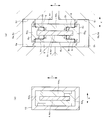
- FIG. 1 is a plan view of a main part of an electronic device according to an embodiment of the present invention.
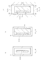
- FIG. 2 is a sectional view of the magnetic component according to the first embodiment of the present invention.
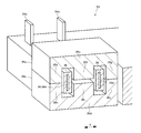
- FIG. 3 is a plan view of the magnetic component of FIG. 2 in a state where a core is omitted.
- FIG. 4 is a perspective view of the coil and the primary molded insulator of FIG.
- FIG. 5 is a sectional view of a main part of the magnetic component of FIG.
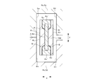
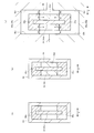
- FIG. 6 is a sectional view of a main part of a magnetic component according to a second embodiment of the present invention.
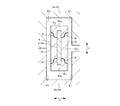
- FIG. 7A is a sectional view of a main part of a magnetic component according to a third embodiment of the present invention.
- FIG. 1 is a plan view of a main part of an electronic device according to an embodiment of the present invention.
- FIG. 2 is a sectional view of the magnetic component according to the first embodiment of the present invention.
- FIG. 3 is
- FIG. 7B is a sectional view of a main part of the magnetic component according to the third embodiment of the present invention.
- FIG. 8A is a sectional view of a main part of a magnetic component according to a fourth embodiment of the present invention.
- FIG. 8B is a sectional view of a main part of the magnetic component according to the fourth embodiment of the present invention.
- FIG. 9 is a sectional view of a main part of a magnetic component according to a fifth embodiment of the present invention.
- FIG. 10 is a sectional view of a main part of a magnetic component according to a sixth embodiment of the present invention.
- FIG. 11 is a plan view of a conventional magnetic component.
- FIG. 12 is a sectional view taken along line BB of FIG.
- FIG. 13 is a diagram showing a state where the core is omitted from FIG.
- FIG. 14 is a sectional view of a main part of the magnetic component of FIG.
- FIG. 15 is a cross-sectional view of
- FIG. 1 is a plan view of a main part of the electronic device 100 according to the embodiment.
- the electronic device 100 is composed of, for example, a DC-DC converter for use in a vehicle.
- the electronic device 100 includes a housing 1, a frame 6, a substrate 2, and various electronic components.
- the electronic component includes a magnetic component 3.
- the housing 1 is made of a metal or synthetic resin radiator, and holds the frame 6.
- the frame 6 is made of a synthetic resin insulator and holds the substrate 2.
- the board 2 is made of a printed board.
- An electric circuit 2 a is mounted on the board 2.
- the magnetic component 3 is formed of a choke coil in this example, and is provided at an end of the frame 6.
- FIGS. 2 to 5 are views showing the magnetic component 3 of the first embodiment.
- FIG. 2 is a cross-sectional view of the magnetic component 3 (a cross-sectional view taken along line AA in FIG. 1).
- FIG. 3 is a plan view of the magnetic component 3 in a state where the cores 5a and 5b are omitted.
- FIG. 4 is a perspective view of the coil 4 and the primary molded insulator 6c of FIG.
- FIG. 5 is a sectional view of a main part of the magnetic component 3.
- the magnetic component 3 includes a coil 4 made of a conductor, cores 5a and 5b made of a magnetic material, and a frame 6 made of an insulator.
- the coil 4 is formed in a U-shape as viewed from above as shown in FIG. 3 by processing a metal plate into a sheet metal.
- the frame 6 is formed by insert molding so as to cover the coil 4.
- the frame 6 has rectangular through holes 6a, 6b arranged side by side.
- One of the through holes 6a is formed inside the coil 4, that is, between two straight portions 4d of the coil 4.
- the other through-hole 6b is formed on the opposite side of the straight portion 4d of the coil 4 from the through-hole 6a (the substrate 2 side in FIG. 1).
- the thinnest portion is around the straight portion 4d of the coil 4.
- terminal portions 4a and 4b for passing a current to the coil 4 are provided.
- Each terminal portion 4a, 4b projects upward from the frame 6, as shown in FIG.
- one ends of electric wires 9a, 9b are electrically connected to the terminal portions 4a, 4b.
- the other ends of the electric wires 9a and 9b are electrically connected to an electric circuit 2a formed on the substrate 2. That is, the coil 4 is electrically connected to the electric circuit 2a via the electric wires 9a and 9b.
- the cores 5a and 5b are made of an E-shaped ferrite core in cross section.
- the upper core 5a on the upper side in FIG. 2 is provided with a base 5c and three protrusions 5e, 5f, 5g.
- the lower core 5b on the lower side is provided with a base 5d and three protrusions 5h, 5i, 5j.
- the cores 5a and 5b are assembled by bringing the tips of the protrusions 5e and 5g at both ends of the upper core 5a into close contact with the tips of the protrusions 5h and 5j at both ends of the lower core 5b.
- the housing 1 supports the lower core 5b from below.
- the cores 5a and 5b are fixed to the housing 1 by being pressed against the housing 1 from above by a fixture (not shown).
- the right protrusions 5g, 5j of the cores 5a, 5b are inserted into the through holes 6b of the frame 6.
- the central protrusions 5f, 5i of the cores 5a, 5b are inserted into the through holes 6a of the frame 6 (see also FIG. 1).
- the left protrusions 5e and 5h of the cores 5a and 5b are arranged near the sides of the frame 6.
- the cores 5a and 5b and the frame 6 are separated from each other. Among the spacings between the cores 5a and 5b and the frame 6, the narrowest is the spacing between the protrusions 5e to 5j of the cores 5a and 5b and the frame 6.
- the coil 4 is wound once between the central protrusions 5f, 5i of the cores 5a, 5b and the protrusions 5e, 5g, 5h, 5j at both ends.
- the coil 4 generates a magnetic flux when energized.
- the cores 5a and 5b form a magnetic path of the magnetic flux generated by the coil 4.
- the frame 6 covers portions other than the terminal portions 4a and 4b of the coil 4, and insulates the coil 4 from the cores 5a and 5b.
- the frame 6 is an example of the “covering member” of the present invention.
- the terminal parts 4a and 4b and the center part 4c of the coil 4 shown in FIG. 3 are held by holding parts (not shown) so that the other parts of the coil 4 do not contact the mold.
- the central portion 4c of the coil 4 is held by a movable holding component that can come and go in the mold.
- the molten synthetic resin forming the frame 6 is filled into the mold from a gate (not shown). Then, the synthetic resin in the molten state flows at a predetermined pressure from the sides of the terminal portions 4a and 4b and the side of the central portion 4c into the periphery of each straight portion 4d, as indicated by arrows in FIG. At this time, there is a possibility that the straight portion 4d is deformed and moved to bend due to the inflow pressure of the synthetic resin and comes into contact with the mold.
- a primary molded insulator (rigid body) 6c already formed in a concave shape with a synthetic resin is attached to the upper and lower ends of the straight portion 4d of the coil 4, and then, as shown in FIG. 2), the coil 4 and the primary molded insulator 6c are loaded into the mold 10.
- the upper and lower ends which are a part of the straight portion 4 d of the coil 4 are held by the primary molding insulator 6 c, and the straight portion 4 d can be positioned at the center in the mold 10. it can.
- the synthetic resin 6d is a secondary molded insulator, and may be the same synthetic resin as the primary molded insulator 6c or a different synthetic resin.
- the frame 6 includes the primary molded insulator 6c and the secondary molded insulator 6d.
- the primary molded insulator 6c is an example of the “first covering portion” of the present invention
- the secondary molded insulator 6d is an example of the “second covering portion” of the present invention.
- the boundary S between the primary molded insulator 6c and the secondary molded insulator 6d is, for example, a thin portion of the frame 6 where the coil 4 and the cores 5a and 5b are closest, as shown by a thick line in FIG. It exists in a portion interposed between the straight portion 4d of the coil 4 and the protrusions 5e to 5j of the cores 5a and 5b.
- FIG. 5C shows a cross section between the protrusions 5e and 5h and the protrusions 5f and 5i of the cores 5a and 5b of the magnetic component 3, but the protrusions 5g and 5j of the cores 5a and 5b and the protrusions.
- the cross section between 5f and 5i has the same structure (not shown). (The same applies to FIG. 6 (c), FIG. 7B (e), FIG. 8B (e), FIG. 9, and FIG. 10, which will be described later.)
- the boundary S is bent toward the cores 5a and 5b from the coil 4.
- the primary molded insulator 6c and a part of the secondary molded insulator 6d are arranged in the left-right direction X that reaches the cores 5a and 5b from the coil 4 in the shortest direction, the boundary S is positioned with respect to the left-right direction X. Bent.
- the boundary S between the primary molded insulator 6c and the secondary molded insulator 6d which is on the upper side in FIG. 5C, extends from the coil 4 by one predetermined length in the left-right direction X, and then extends in the left-right direction. In the vertical direction Y perpendicular to X, it is bent upward and extends upward, and reaches the upper surface 6u different from the left surface 6L and the right surface 6r of the frame 6 having the smallest interval with the upper core 5a. I have.
- the boundary S between the primary molded insulator 6c and the secondary molded insulator 6d on the lower side extends a predetermined length from the coil 4 in one of the left and right directions X and then is perpendicular to the left and right directions X. It is bent downward in the vertical direction Y and extends downward, and reaches a lower surface 6v different from the left and right surfaces 6L and 6r of the frame 6.
- the primary molded insulator 6c and a part of the secondary molded insulator 6d of the frame 6 are arranged in the left-right direction X that reaches the shortest from the coil 4 to the cores 5a and 5b. Therefore, the boundary S between the primary molded insulator 6c and the secondary molded insulator 6d is extended from the coil 4 in the left-right direction X, and then bent in the vertical direction Y perpendicular to the left-right direction X. The length of the boundary S can be easily increased.
- the boundary S between the primary molded insulator 6c and the secondary molded insulator 6d extends from the coil 4 and is bent, the boundary S between the cores 5a and 5b is the smallest. It reaches upper and lower surfaces 6u and 6v different from left and right surfaces 6L and 6r. Therefore, insulation between the creepage distance D 1 + D 2 + D 3 and the insulation distance D 1 + D 2 + D 3 + D 4 and to maximize long coil 4 and cores 5a, 5b between the coil 4 and cores 5a, 5b Performance can be further improved.
- FIG. 6 is a cross-sectional view of a main part of the magnetic component 3 according to the second embodiment.
- a primary molded insulator 6e shown in FIG. Attach to upper and lower ends of 4d.
- the primary molded insulator 6e includes a first engaging portion 6f that engages with upper and lower ends of the coil 4 so that the straight portion 4d of the coil 4 does not shift in the mold 10, and a primary molded insulator 6e. It has a second engagement portion 6g that engages with the mold 10 so as not to be displaced, and a step portion 6h provided between the engagement portions 6f and 6g.
- the primary molded insulator 6e may be the same synthetic resin as a secondary molded insulator 6d described later, or may be a different synthetic resin.
- the straight portion 4d of the coil 4 is also shifted left and right.
- the position shifts in the direction X.
- the straight molded portion 4d of the coil 4 and one of the convex portions 5e to 5j of the cores 5a and 5b are in contact with each other. There is a possibility that the creepage distance and the insulation distance between them may become short.
- the second engaging portion 6g of the primary molded insulator 6e is not only in contact with the mold 10 from the vertical direction Y but also from the horizontal direction X.
- the straight portion 4d of the coil 4 engaged with the first engaging portion 6f of the primary molded insulator 6e is not displaced in the left-right direction X, and the straight portion 4d is securely held at the center in the mold 10. can do.
- step portion 6h is provided in the primary molded insulator 6e, as shown by a thick line in FIG. 6C, a step is formed at the boundary S between the primary molded insulator 6e and the secondary molded insulator 6d. Since St is formed, the length (creepage distance) D 1 + D 5 + D 3 of the boundary S is increased, and the insulation distance between the straight portion 4d of the coil 4 and the protrusions 5e to 5j of the cores 5a and 5b is increased. D 1 + D 5 + D 3 + D 4 can also be easily lengthened. Therefore, the insulation between the coil 4 of the magnetic component 3 and the cores 5a and 5b can be improved.
- FIG. 7A and 7B are cross-sectional views of main parts of the magnetic component 3 according to the third embodiment.
- the upper and lower ends of the straight portion 4d are movable holding parts. Hold at 11.
- the movable holding component 11 is a movable component provided in the mold 10 and can be moved into and out of the mold 10 by a driving mechanism (not shown).
- the shape of the portion of the movable holding component 11 protruding into the mold 10 is the same as the shape of the primary molded insulator 6c (see FIG. 5A) used in the first embodiment.
- the frame 6 is configured by the primary fill insulation 6d 1 and the secondary fill insulation 6d 2.
- the intermediate portion of the straight portion 4d of the coil 4 is covered by the primary fill insulation 6d 1, the upper and lower ends of the straight portion 4d is covered by the secondary fill insulation 6d 2.
- Primary fill boundary S of the insulator 6d 1 and the secondary fill insulation 6d 2 like the first embodiment, towards the core 5a, the 5b in a state bent from the coil 4.
- Primary fill insulation 6d 1 is an example of the "first covering portion" of the present invention
- the secondary fill insulation 6d 2 is an example of the "second covering portion" in the present invention.
- a movable holding part 11 even by insert molding the frame 6, as shown by a thick line in FIG. 7B (e), 1 primary fill insulation 6d 1 and the secondary fill insulation longer length D 1 + D 2 of the boundary S of the body 6d 2, straight portions 4d and the core 5a of the coil 4, creepage distances D 1 + D 2 + D 3 and insulation distance between the 5b of the projections 5e ⁇ 5j Since D 1 + D 2 + D 3 + D 4 is also longer, it is possible to improve the insulation between the coil 4 of the magnetic component 3 and the cores 5a and 5b.
- FIGS. 8A and 8B are cross-sectional views of main parts of the magnetic component 3 of the fourth embodiment.
- the upper and lower ends of the straight portion 4d of the coil 4 are held by the movable holding component 12 in the mold 10 during the insert molding of the frame 6, as shown in FIG.
- the shape of the portion of the movable holding component 12 protruding into the mold 10 is the same as the shape of the primary molded insulator 6e (see FIG. 6A) used in the second embodiment.
- the movable holding component 12 has a first engagement portion 12f that engages with the upper and lower ends of the coil 4 so that the straight portion 4d of the coil 4 does not shift in the mold 10, and the movable holding component 12 does not shift.
- a second engaging portion 12g that engages with the mold 10, and a step portion 12h provided between the engaging portions 12f and 12g.
- the first engaging portion 12f of the movable holding component 12 engages with the upper and lower ends of the straight portion 4d of the coil 4 during insert molding, and the second engaging portion 12g engages with the mold 10. by coupling, it can be prevented during the filling of the primary fill insulation 6d 1, that the straight portion 4d and the movable holding part 12 of the coil 4 is being displaced in the lateral direction X by the inflow pressure. Further, when the secondary fill insulation 6d 2 fill, the intermediate portion of the straight portion 4d of the coil 4 is held by the primary fill insulation 6d 1, straight portion by inflow pressure of the secondary fill insulation 6d 2 4d can be prevented from shifting in the left-right direction X.
- the primary fill insulation 6d 1 and the secondary fill insulation 6d 2 is cured, the frame 6 and the core 5a, and the 5b are combined, as shown by a thick line in FIG. 8B (e), primary filling
- the length (creepage distance) D 1 + D 5 + D 3 of the boundary S between the insulator 6d 1 and the secondary filling insulator 6d 2 becomes longer, and the straight portion 4d of the coil 4 and the convex portions 5e to 5j of the cores 5a, 5b.
- the insulation distance D 1 + D 5 + D 3 + D 4 between them can be increased.
- step St is formed at the boundary S of the primary fill insulation 6d 1 and the secondary fill insulation 6d 2
- the length of the boundary S (Creepage distance) D 1 + D 5 + D 3 and insulation distance D 1 + D 5 + D 3 + D 4 can be easily increased. Therefore, the insulation between the coil 4 of the magnetic component 3 and the cores 5a and 5b can be improved.
- the present invention can employ various embodiments other than those described above.
- the example in which the boundary S of the frame 6 is directed from the coil 4 toward the cores 5a and 5b is shown, but the present invention is not limited to this.
- the corners of the primary molded insulator 6c 'of the frame 6 are processed into a curved surface having a predetermined radius of curvature, so that the primary molded insulator 6c' is formed.
- the boundary S between 6c 'and the secondary molded insulator 6d may be curved toward the cores 5a and 5b from the coil 4.
- the corners of the movable holding parts 11 and 12 may be formed into curved surfaces having a predetermined radius of curvature. Again, the boundary S between the primary fill insulation 6d 1 and the secondary fill insulation 6d 2 frame 6, the core 5a, so towards 5b in a state of being curved from the coil 4.
- the curing conditions and the die 1 was filled into 10 primary fill insulation 6d 1, and timing of movement of the mold 10 outside of the movable holding parts 11, 12, the secondary fill insulation 6d 2 die 10 such as by adjusting the timing of the filling of the inner boundary S of the primary fill insulation 6d 1 and the secondary fill insulation 6d 2 is the core 5a in a state of being curved from the coil 4, also be directed to 5b Good.
- the boundary S of the frame 6 is bent or curved once from the coil 4 and reaches the upper surface 6u or the lower surface 6v of the frame 6. 6, 8B, and 10, the boundary S of the frame 6 is bent or bent twice from the coil 4 and reaches the left surface 6L or the right surface 6r of the frame 6. Examples have been given. However, the present invention is not limited to these, and the number of times of bending or bending of the boundary S of the frame 6 from the coil 4 toward the cores 5a and 5b may be three or more.
- the boundary S of the primary molded insulator 6c, 6e, 6c 'and or boundary S between the secondary molded insulator 6d, the primary fill insulation 6d 1 and the secondary fill insulation 6d 2 frames 6, It may be configured to reach any one of the surfaces 6u, 6v, 6L, and 6r of the frame 6 in a state where the coil 4 is bent or curved a suitable number of times.
- one or more steps St may be provided at the boundary S. Further, the boundary S having the step St may reach any of the surfaces 6u, 6v, 6L, 6r of the frame 6.
- the upper and lower ends of the straight portion 4d are connected to the primary molded insulators 6c, 6e, 6c 'and the movable holding component 11,
- the example held at 12 is shown, the present invention is not limited to this.
- one of the upper end and the lower end of the straight portion 4d of the coil 4 may be held by the primary molded insulators 6c, 6e, 6c 'or the movable holding components 11, 12.
- one of the upper end and the lower end of the straight portion 4d may be held by the primary molded insulators 6c, 6e, 6c ', and the other may be held by the movable holding components 11, 12.
- the intermediate portion of the straight portion 4d may be held by the primary molded insulators 6c, 6e, 6c 'and the movable holding components 11, 12.
- one or more of the straight portions 4d are replaced with the primary molded insulators 6c, 6e, 6c 'so that the straight portion 4d of the coil 4 is not deformed by the inflow pressure of the synthetic resin into the mold 10.
- the movable holding parts 11 and 12 may be used.
- the coil 4 is covered with a part of the frame 6 to insulate the coil 4 from the cores 5a and 5b, but the present invention is not limited to this.
- the coil 4 may be covered with a covering member separate from the frame 6 to insulate the coil 4 from the cores 5a and 5b.
- the covering member may be fixed to the housing 1 or the frame 6 of the electronic device 100.
- a core is formed by vertically combining two ferrite cores 5a and 5b having an E-shaped cross section
- the core may be configured by combining an E-shaped core with an I-shaped cross-section.
- only one core having another shape may be used, or a core may be formed by combining three or more cores.
- a core formed of a magnetic material other than ferrite may be used.
- the present invention can be applied to other magnetic components such as a transformer. .
- the present invention is applied to the electronic device 100 including the on-vehicle DC-DC converter and the magnetic component 3 provided in the electronic device 100 has been described.
- the present invention can be applied to electronic devices, electronic devices other than those mounted on vehicles, and magnetic components provided therein.
Landscapes
- Engineering & Computer Science (AREA)
- Power Engineering (AREA)
- Manufacturing & Machinery (AREA)
- Insulating Of Coils (AREA)
Abstract
電子装置に備わる磁気部品(3)は、通電されることにより磁束を発生する導体から成るコイル(4)と、その磁束の磁路を形成する磁性体から成るコア(5a、5b)と、コイル(4)を被覆するようにインサート成形により形成され、コイル(4)とコア(5a、5b)とを絶縁する絶縁体から成るフレーム(6)とを備える。フレーム(6)は、インサート成形時に金型内でコイル(4)の真直部(4d)を位置決めするように真直部(4d)の一部を保持および被覆する1次成形絶縁体(6c)と、真直部(4d)の残部を被覆する2次成形絶縁体(6d)とから構成され、1次成形絶縁体(6c)と2次成形絶縁体(6d)との境界(S)は、真直部(4d)から屈曲した状態でコア(5a、5b)へ向かっている。
Description
本発明は、コイルとコアとを備えた磁気部品と、当該磁気部品を備えた電子装置に関し、特にコイルとコアの絶縁構造に関する。
たとえばDC-DCコンバータのような電子装置には、チョークコイルやトランスなどの磁気部品が備わっている。一般に、そのような磁気部品は、コイルとコアとを有している。コイルは、導体から成り、通電されることにより磁束を発生する。コアは、磁性体にから成り、コイルの大部分を覆うように設けられ、コイルが発生した磁束の磁路を形成する。
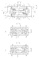
図11~図15は、従来の磁気部品を示した図である。詳しくは、図11は、従来の磁気部品30の平面図、図12は、図11のB-B断面図、図13は、図11からコアを除いた状態を示した図、図14は、磁気部品30の要部の断面図である。図15は、従来の他の磁気部品の要部の断面図である。
磁気部品30は、たとえばチョークコイルから構成されている。磁気部品30のコアは、図12に示すように、断面がE形のフェライトコア35a、35bを上下に組み合わせて構成されている。詳しくは、各コア35a、35bには、3つの凸部35e、35f、35g、35h、35i、35jが設けられていて、そのうち上コア35aの両端にある凸部35e、35gの先端と、下コア35bの両端にある凸部35h、35jの先端とを密着させることで、コア35a、35bは組み立てられている。各コア35a、35bの中央にある凸部35f、35iの周囲には、コイル34が1回巻回されている。コイル34は、金属板を板金加工することにより形成されている(図13参照)。
磁気部品30の性能を確保するため、コイル34を合成樹脂などの絶縁体から成る被覆部材36により被覆することで、コイル34とコア35a、35bとは絶縁されている。
被覆部材36は、コイル34を被覆するようにインサート成形により形成されている。そのインサート成形時に、図13に示すコイル34の両端部34a、34bと中央部34cは保持部品により保持されて、コイル34のそれら以外の部分が金型に接触しないように位置決めされる。図14(a)は、コイル34の真直部34dが金型40内の中央に配置された状態の断面を示している。
上記コイル34の位置決め状態で、被覆部材36を構成する溶融状態の合成樹脂が金型40内に充填される。この際、図13に矢印で示すように、合成樹脂がコイル34の端部34a、34bと中央部34cの側方から真直部34dの周囲に所定の圧力で流れ込む。その合成樹脂の流入圧力により、たとえば図14(b)に示すように、コイル34の真直部34dが変形して(撓んで)移動し、金型40に接触するおそれがある。この状態で合成樹脂が硬化すると、図14(c)に示すように、コイル34の真直部34dが被覆部材36から露出して、該真直部34dとコア35a、35bの凸部35e、35hとの絶縁距離δが短くなり、コイル34とコア35a、35bとの間で絶縁不良が生じて、磁気部品30の性能が損われてしまう。
上記の対策として、図15(a)に示すように、既に合成樹脂で形成された1次成形絶縁体(剛体)36cでコイル34の真直部34dの上下端部を保持して、真直部34dを位置決めした状態で、図15(b)に示すように、溶融状態の合成樹脂(2次成形絶縁体)36dを金型40内に充填する被覆部材36のインサート成形方法がある。このような方法は、たとえば特許文献1に開示されている。
しかしながら、図15のように被覆部材36をインサート成形すると、後から充填された2次成形絶縁体36dの硬化後に、図15(c)に太線で示すように、1次成形絶縁体36cと2次成形絶縁体36dとの境界S’が、コイル34からコア35a、35bまで最短で到達するX方向に一直線に形成される。そして、インサート成形時の状況により、境界S’がピンホールのような脆弱な状態になった場合、境界S’の箇所で絶縁抵抗が低下する。しかも、境界S’の長さすなわち沿面距離Daが短いので、コイル34からコア35a、35bまでの絶縁距離(境界S’の長さDa+被覆部材36と凸部35e、35fとの離間距離Db)も短くなり、コイル34とコア35a、35bとの間で絶縁不良が生じ易くなる。
本発明は、コイルとコアとの絶縁性を向上させることを課題とする。
本発明の磁気部品は、通電されることにより磁束を発生する導体から成るコイルと、その磁束の磁路を形成する磁性体から成るコアと、コイルを被覆するようにインサート成形により形成され、コイルとコアとを絶縁する絶縁体から成る被覆部材とを備える。そして、被覆部材は、インサート成形時に金型内でコイルを位置決めするようにコイルの一部を保持または被覆する第1被覆部と、コイルの残部を被覆する第2被覆部とから構成され、第1被覆部と第2被覆部との境界は、コイルから屈曲または湾曲した状態でコアへ向かっている。
また、本発明の電子装置は、上記磁気部品と、上記磁気部品のコイルが電気的に接続された基板と、磁気部品と基板とを保持する筐体とを備える。
上記によると、被覆部材の第1被覆部と第2被覆部との境界が屈曲または湾曲している分、当該境界の長さが従来に比べて長くなっている。このため、被覆部材のインサート成形時の状況により、第1被覆部と第2被覆部との境界がピンホールのような脆弱な状態になっていても、当該境界の長さを含む沿面距離が長くなり、コイルからコアまでの絶縁距離も長くなるので、コイルとコアとの間の絶縁性を向上させることが可能となる。
また、本発明では、被覆部材の第1被覆部と第2被覆部の一部とは、コイルからコアまで最短で到達する方向に並んでいて、当該方向に対して第1被覆部と第2被覆部との境界が屈曲または湾曲していてもよい。
また、本発明において、第1被覆部と第2被覆部との境界は、コイルから屈曲または湾曲した状態で、コアとの間隔が最も狭い被覆部材の第1表面とは異なる第2表面に到達していてもよい。
また、本発明において、第1被覆部と第2被覆部との境界に段差が設けられていてもよい。
また、本発明において、被覆部材の第1被覆部は、インサート成形前に形成されて、インサート成形時にコイルの一部に装着される1次成形絶縁体から構成され、第2被覆部は、インサート成形時にコイルの残部と1次成形絶縁体の周囲に充填された2次成形絶縁体から構成されていてもよい。
また、本発明において、1次成形絶縁体は、金型内でコイルが位置ずれしないようにコイルの一部と係合する第1係合部と、当該1次成形絶縁体が位置ずれしないように金型と係合する第2係合部と、第1係合部と第2係合部との間に設けられた段差部と、を有していてもよい。
または、本発明において、被覆部材の第1被覆部は、インサート成形時にコイルの一部が可動保持部品で保持された状態で、金型内に充填された1次充填絶縁体から構成され、第2被覆部は、インサート成形時に可動保持部品が金型外へ移動して生じる金型内の空間に充填された2次充填絶縁体から構成されていてもよい。
本発明によれば、コイルとコアとの絶縁性を向上させることが可能となる。
以下、本発明の実施形態につき、図面を参照しながら説明する。各図において、同一の部分または対応する部分には、同一符号を付してある。
図1は、実施形態の電子装置100の要部の平面図である。電子装置100は、たとえば車載用のDC-DCコンバータから構成されている。電子装置100には、筐体1、フレーム6、基板2、および種々の電子部品が備わっている。その電子部品には、磁気部品3が含まれている。
筐体1は、金属製または合成樹脂製の放熱体から成り、フレーム6を保持している。フレーム6は、合成樹脂製の絶縁体から成り、基板2を保持している。基板2は、プリント基板から成る。基板2には、電気回路2aが実装されている。磁気部品3は、本例ではチョークコイルから成り、フレーム6の端部に設けられている。
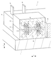
図2~図5は、第1実施形態の磁気部品3を示した図である。詳しくは、図2は、磁気部品3の断面図(図1のA-A断面図)である。図3は、磁気部品3のコア5a、5bを省略した状態の平面図である。図4は、図2のコイル4と1次成形絶縁体6cの斜視図である。図5は、磁気部品3の要部の断面図である。
図2に示すように、磁気部品3には、導体から成るコイル4、磁性体から成るコア5a、5b、および絶縁体から成るフレーム6が備わっている。
コイル4は、金属板を板金加工することにより、図3に示すように上方から見てU形に形成されている。フレーム6は、コイル4を被覆するようにインサート成形により形成されている。
フレーム6には、矩形状の貫通孔6a、6bが並設されている。そのうち、一方の貫通孔6aは、コイル4の内側、すなわちコイル4の2つの真直部4dの間に形成されている。他方の貫通孔6bは、コイル4の一方の真直部4dに対して貫通孔6aと反対側(図1で基板2側)に形成されている。コイル4を被覆するフレーム6の被覆部分のうち、最も肉厚が薄い部分はコイル4の真直部4dの周囲である。
コイル4の両端には、コイル4に電流を流すための端子部4a、4bが設けられている。各端子部4a、4bは、図2に示すように、フレーム6から上方に突出している。図1に示すように、各端子部4a、4bには、電気配線9a、9bの一端が電気的に接続されている。各電気配線9a、9bの他端は、基板2に形成された電気回路2aに電気的に接続されている。すなわち、コイル4は、電気配線9a、9bを介して電気回路2aに電気的に接続されている。
図2に示すように、コア5a、5bは、断面がE形のフェライトコアから成る。図2で上側にある上コア5aには、基部5cと3つの凸部5e、5f、5gが設けられている。下側にある下コア5bには、基部5dと3つの凸部5h、5i、5jが設けられている。上コア5aの両端にある凸部5e、5gの先端と下コア5bの両端にある凸部5h、5jの先端とを密着させることで、コア5a、5bは組み立てられている。筐体1は、下コア5bを下方から支持している。コア5a、5bは、図示しない固定金具により上側から筐体1に押し付けられることで、筐体1に固定されている。
図2でコア5a、5bの右側の凸部5g、5jは、フレーム6の貫通孔6bに挿通されている。コア5a、5bの中央の凸部5f、5iは、フレーム6の貫通孔6a(図1も参照)に挿通されている。コア5a、5bの左側の凸部5e、5hは、フレーム6の側方近傍に配置されている。
コア5a、5bとフレーム6とは離間している。コア5a、5bとフレーム6との離間間隔のうち、最も狭いのは、コア5a、5bの凸部5e~5jとフレーム6との間隔である。
コイル4は、コア5a、5bの中央の凸部5f、5iと両端の凸部5e、5g、5h、5jとの間に1回巻回されている。コイル4は、通電されることにより磁束を発生する。コア5a、5bは、コイル4が発生した磁束の磁路を形成する。
フレーム6は、コイル4の端子部4a、4b以外を被覆し、コイル4とコア5a、5bとを絶縁している。フレーム6は、本発明の「被覆部材」の一例である。
磁気部品3の性能を確保するには、フレーム6によりコイル4を確実に被覆して、コイル4とコア5a、5bとの絶縁性を高める必要がある。
そのため、フレーム6のインサート成形時に、図示しない保持部品により、図3に示すコイル4の端子部4a、4bと中央部4cを保持して、コイル4のそれら以外の部分が金型に接触しないように位置決めする。コイル4の中央部4cは、金型内に対して出没可能な可動保持部品により保持する。
フレーム6を形成する溶融状態の合成樹脂は、図示しないゲートから金型内に充填される。そして、溶融状態の合成樹脂は、図3に矢印で示すように、コイル4の端子部4a、4bの側方と中央部4cの側方から各真直部4dの周囲に所定の圧力で流れ込む。この際、合成樹脂の流入圧力により、真直部4dが撓むように変形して移動し、金型に接触するおそれがある。
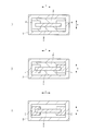
そこで、図4に示すように、既に合成樹脂で凹形に形成された1次成形絶縁体(剛体)6cを、コイル4の真直部4dの上下端部に装着してから、図5(a)に示すようにコイル4と1次成形絶縁体6cとを金型10内に装填する。これにより、金型10内において、コイル4の真直部4dの一部である上下端部を1次成形絶縁体6cにより保持して、真直部4dを金型10内の中央に位置決めすることができる。
そして、溶融状態の合成樹脂が金型10内へ流入したときに、図5(b)に示すように、1次成形絶縁体6cによるコイル4の真直部4dの位置決め状態が維持されるので、真直部4dが変形して金型10に接触することを防止することができる。
図5(a)に示すように、コイル4の真直部4dの板厚方向(図5で左右方向)Xに対して、1次成形絶縁体6cと金型10との間、および1次成形絶縁体6cで覆われていない真直部4dの残部(中間部)と金型10との間には、隙間Tが設けられている。このため、図5(b)に示すように、溶融状態の合成樹脂6dが、金型10内の隙間T、すなわちコイル4の真直部4dの中間部と1次成形絶縁体6cの周囲に充填される。合成樹脂6dは、2次成形絶縁体であり、1次成形絶縁体6cと同一の合成樹脂であってもよいし、異なる合成樹脂であってもよい。
その後、2次成形絶縁体6dが硬化することで、コイル4の真直部4dの上下端部が1次成形絶縁体6cにより被覆され、真直部4dの中間部が2次成形絶縁体6dにより被覆される。つまり、フレーム6は、1次成形絶縁体6cと2次成形絶縁体6dにより構成されている。1次成形絶縁体6cは、本発明の「第1被覆部」の一例であり、2次成形絶縁体6dは、本発明の「第2被覆部」の一例である。
1次成形絶縁体6cと2次成形絶縁体6dの境界Sは、たとえば図5(c)に太線で示すように、コイル4とコア5a、5bとが最も接近するフレーム6の肉薄部分、すなわちコイル4の真直部4dとコア5a、5bの凸部5e~5jの間に介在する部分に存在している。図5(c)は、磁気部品3のコア5a、5bの凸部5e、5hと凸部5f、5iの間の断面を示しているが、コア5a、5bの凸部5g、5jと凸部5f、5iの間の断面も同様の構造である(図示省略)。(後述する図6(c)、図7B(e)、図8B(e)、図9、および図10も同様である。)
図5(c)に太線で示すように、境界Sはコイル4から屈曲した状態でコア5a、5bへ向かっている。また、コイル4からコア5a、5bまで最短で到達する左右方向Xに、1次成形絶縁体6cと2次成形絶縁体6dの一部とが並んでいるため、境界Sは左右方向Xに対して屈曲している。
詳しくは、図5(c)で上側にある1次成形絶縁体6cと2次成形絶縁体6dの境界Sは、コイル4から左右方向Xのうちいずれか一方へ所定長延びた後、左右方向Xに対して垂直な上下方向Yのうち上方向へ屈曲して上方へ延び、上コア5aとの間隔が最も狭いフレーム6の左表面6Lや右表面6rとは異なる上表面6uに到達している。また、下側にある1次成形絶縁体6cと2次成形絶縁体6dとの境界Sは、コイル4から左右方向Xのうちいずれか一方へ所定長延びた後、左右方向Xに対して垂直な上下方向Yのうち下方向へ屈曲して下方へ延び、フレーム6の左右表面6L、6rとは異なる下表面6vに到達している。
フレーム6のインサート成形時の状況により、1次成形絶縁体6cと2次成形絶縁体6dとの境界Sが、ピンホールのような脆弱な状態になった場合、境界Sの箇所で絶縁抵抗が低下する。然るに、図5(c)に示すように境界Sが屈曲している分、境界Sの長さD1+D2が、図15(c)に示した従来の境界S’の長さDaより長くなっている。このため、境界Sの長さD1+D2を含む沿面距離D1+D2+D3や、コイル4の真直部4dからコア5a、5bの凸部5e~5jまでの絶縁距離D1+D2+D3+D4も長くなり、コイル4とコア5a、5bとの絶縁不良を生じ難くすることができる。よって、上記第1実施形態によると、磁気部品3のコイル4とコア5a、5bとの絶縁性を向上させることが可能となる。
また、上記第1実施形態では、フレーム6の1次成形絶縁体6cと2次成形絶縁体6dの一部とを、コイル4からコア5a、5bまで最短で到達する左右方向Xに並べている。このため、1次成形絶縁体6cと2次成形絶縁体6dとの境界Sを、コイル4から左右方向Xへ延ばした後、左右方向Xに対して垂直な上下方向Yへ屈曲させることで、境界Sの長さを容易に長くすることができる。そして、コイル4とコア5a、5bとの間の沿面距離D1+D2+D3および絶縁距離D1+D2+D3+D4を十分に確保して、コイル4とコア5a、5bとの絶縁性をより向上させることが可能となる。
さらに、上記第1実施形態では、1次成形絶縁体6cと2次成形絶縁体6dとの境界Sが、コイル4から延びて屈曲した後、コア5a、5bとの間隔が最も狭いフレーム6の左右表面6L、6rとは異なる上下表面6u、6vに到達している。このため、コイル4とコア5a、5bとの間の沿面距離D1+D2+D3および絶縁距離D1+D2+D3+D4を最大限長くして、コイル4とコア5a、5bとの絶縁性を一層向上させることが可能となる。
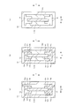
図6は、第2実施形態の磁気部品3の要部の断面図である。第2実施形態では、フレーム6のインサート成形時に、図5(a)に示した1次成形絶縁体6cに代えて、図6(a)に示す1次成形絶縁体6eをコイル4の真直部4dの上下端部に装着する。
1次成形絶縁体6eは、金型10内でコイル4の真直部4dが位置ずれしないようにコイル4の上下端部と係合する第1係合部6fと、1次成形絶縁体6eが位置ずれしないように金型10と係合する第2係合部6gと、これらの係合部6f、6gの間に設けられた段差部6hとを有している。また、1次成形絶縁体6eは、後述する2次成形絶縁体6dと同一の合成樹脂であってもよいし、異なる合成樹脂であってもよい。
フレーム6のインサート成形時に、溶融状態の2次成形絶縁体6dの流入圧力により、金型10内で1次成形絶縁体6eが左右方向Xに位置ずれした場合、コイル4の真直部4dも左右方向Xに位置ずれする。この位置ずれ状態で、2次成形絶縁体6dが硬化して、フレーム6とコア5a、5bとが組み合わされると、コイル4の真直部4dとコア5a、5bの凸部5e~5jのいずれかとの間の沿面距離および絶縁距離が短くなるおそれがある。
然るに、上記第2実施形態によると、図6(b)に示すように、1次成形絶縁体6eの第2係合部6gが金型10と上下方向Yからだけでなく左右方向Xからも係合することで、溶融状態の2次成形絶縁体6dの流入圧力により1次成形絶縁体6eが左右方向Xに位置ずれするのを阻止することができる。このため、1次成形絶縁体6eの第1係合部6fに係合したコイル4の真直部4dも左右方向Xに位置ずれせず、真直部4dを金型10内の中心に確実に保持することができる。そして、その状態で2次成形絶縁体6dが硬化して、フレーム6とコア5a、5bとが組み合わされると、図6(c)に示すように、コイル4の真直部4dとコア5a、5bの凸部5e~5jとの間の沿面距離D1+D5+D3および絶縁距離D1+D5+D3+D4を長く確保することができる。
また、1次成形絶縁体6eに段差部6hが設けられたことで、図6(c)に太線で示すように、1次成形絶縁体6eと2次成形絶縁体6dとの境界Sに段差Stが形成されるので、境界Sの長さ(沿面距離)D1+D5+D3を長くして、コイル4の真直部4dとコア5a、5bの凸部5e~5jとの間の絶縁距離D1+D5+D3+D4も容易に長くすることができる。よって、磁気部品3のコイル4とコア5a、5bとの絶縁性を向上させることが可能となる。
図7Aおよび図7Bは、第3実施形態の磁気部品3の要部の断面図である。第3実施形態では、フレーム6のインサート成形時に金型10内でコイル4の真直部4dを位置決めするために、図7A(a)に示すように、真直部4dの上下端部を可動保持部品11で保持する。可動保持部品11は、金型10に備わる可動部品であって、図示しない駆動機構により、金型10内に対して出没可能になっている。また、可動保持部品11の金型10内に突出する部分の形状は、第1実施形態で用いた1次成形絶縁体6c(図5(a)参照)の形状と同一である。
図7A(a)の状態から、フレーム6を形成する溶融状態の合成樹脂6d1を金型10内に充填する。このとき充填された合成樹脂6d1は1次充填絶縁体であって、図7A(b)に示すようにコイル4の真直部4dと可動保持部品11の周囲に行き渡る。次に、1次充填絶縁体6d1が完全に硬化する前に、可動保持部品11を金型10外へ移動させて、コイル4の真直部4dの保持を解放する。これにより、図7A(c)に示すように金型10内に可動保持部品11の抜け跡である空間Qが生じる。また、コイル4の真直部4dの中央部が1次充填絶縁体6d1により保持されて、真直部4dが位置決めされた状態となる。
そしてさらに、図7B(d)に示すように、溶融状態の合成樹脂6d2を金型10内に充填する。このとき充填された合成樹脂6d2は2次充填絶縁体であって、図7A(c)に示した空間Qに行き渡る。またこのとき、コイル4の真直部4dの中央部が1次充填絶縁体6d1により保持されているので、2次充填絶縁体6d2の流入圧力により真直部4dが左右方向Xに位置ずれするのを阻止することができる。
その後、1次充填絶縁体6d1と2次充填絶縁体6d2が硬化することで、フレーム6が、1次充填絶縁体6d1と2次充填絶縁体6d2により構成される。そして、コイル4の真直部4dの中間部が1次充填絶縁体6d1により被覆され、真直部4dの上下端部が2次充填絶縁体6d2により被覆される。1次充填絶縁体6d1と2次充填絶縁体6d2の境界Sは、第1実施形態と同様に、コイル4から屈曲した状態でコア5a、5bへ向かっている。1次充填絶縁体6d1は、本発明の「第1被覆部」の一例であり、2次充填絶縁体6d2は、本発明の「第2被覆部」の一例である。
上記第3実施形態のように、可動保持部品11を用いて、フレーム6をインサート成形しても、図7B(e)に太線で示すように、1次充填絶縁体6d1と2次充填絶縁体6d2の境界Sの長さD1+D2が長くなって、コイル4の真直部4dとコア5a、5bの凸部5e~5jとの間の沿面距離D1+D2+D3や絶縁距離D1+D2+D3+D4も長くなるので、磁気部品3のコイル4とコア5a、5bとの絶縁性を向上させることが可能となる。
図8Aおよび図8Bは、第4実施形態の磁気部品3の要部の断面図である。第4実施形態では、フレーム6のインサート成形時に金型10内で、図8A(a)に示すように、コイル4の真直部4dの上下端部を可動保持部品12で保持する。可動保持部品12の金型10内に突出する部分の形状は、第2実施形態で用いた1次成形絶縁体6e(図6(a)参照)の形状と同一である。
可動保持部品12は、金型10内でコイル4の真直部4dが位置ずれしないようにコイル4の上下端部と係合する第1係合部12fと、可動保持部品12が位置ずれしないように金型10と係合する第2係合部12gと、これらの係合部12f、12gの間に設けられた段差部12hとを有している。
図8A(a)の状態から、フレーム6を形成する溶融状態の1次充填絶縁体6d1を金型10内に充填する(図8A(b)の状態)。次に、1次充填絶縁体6d1が完全に硬化する前に、可動保持部品12を金型10外へ移動させて、図8A(c)に示すようにコイル4の真直部4dの保持を解放する。これにより、金型10内に空間Qが生じる。そしてさらに、溶融状態の2次充填絶縁体6d2を金型10内に充填して空間Qに行き渡らせる。この後、1次充填絶縁体6d1と2次充填絶縁体6d2を硬化させて、コイル4の真直部4dを1次充填絶縁体6d1と2次充填絶縁体6d2により被覆する(図8B(d)の状態)。
上記第4実施形態によると、インサート成形時に可動保持部品12の第1係合部12fがコイル4の真直部4dの上下端部に係合し、第2係合部12gが金型10と係合することで、1次充填絶縁体6d1の充填時に、その流入圧力によりコイル4の真直部4dや可動保持部品12が左右方向Xに位置ずれするのを阻止することができる。また、2次充填絶縁体6d2の充填時に、コイル4の真直部4dの中間部が1次充填絶縁体6d1により保持されているので、2次充填絶縁体6d2の流入圧力により真直部4dが左右方向Xに位置ずれするのを阻止することができる。そして、1次充填絶縁体6d1と2次充填絶縁体6d2が硬化して、フレーム6とコア5a、5bとが組み合わされると、図8B(e)に太線で示すように、1次充填絶縁体6d1と2次充填絶縁体6d2の境界Sの長さ(沿面距離)D1+D5+D3が長くなって、コイル4の真直部4dとコア5a、5bの凸部5e~5jとの間の絶縁距離D1+D5+D3+D4も長くすることができる。
また、可動保持部品12に段差部12hが設けられたことで、1次充填絶縁体6d1と2次充填絶縁体6d2との境界Sに段差Stが形成されるので、境界Sの長さ(沿面距離)D1+D5+D3、および絶縁距離D1+D5+D3+D4を容易に長くすることができる。よって、磁気部品3のコイル4とコア5a、5bとの絶縁性を向上させることが可能となる。
本発明は、上述した以外にも種々の実施形態を採用することができる。たとえば、以上の実施形態では、フレーム6の境界Sが、コイル4から屈曲した状態でコア5a、5bに向かう例を示したが、本発明はこれのみに限定するものではない。これ以外に、たとえば図9に示す第5実施形態のように、フレーム6の1次成形絶縁体6c’の角部を所定の曲率半径をもった曲面に加工することにより、1次成形絶縁体6c’と2次成形絶縁体6dとの境界Sが、コイル4から湾曲した状態でコア5a、5bに向かうようにしてもよい。
また、フレーム6の1次成形絶縁体6c、6e、6c’に代えて、可動保持部品11、12でコイル4の真直部4dを位置決めする場合は、図10に示す第6実施形態のように、可動保持部品11、12の角部を所定の曲率半径をもった曲面に加工してもよい。この場合も、フレーム6の1次充填絶縁体6d1と2次充填絶縁体6d2との境界Sが、コイル4から湾曲した状態でコア5a、5bに向かうようになる。
また、金型10内に充填した1次充填絶縁体6d1の硬化状態や、可動保持部品11、12の金型10外への移動のタイミングや、2次充填絶縁体6d2の金型10内への充填のタイミングなどを調整して、1次充填絶縁体6d1と2次充填絶縁体6d2との境界Sが、コイル4から湾曲した状態でコア5a、5bに向かうようにしてもよい。
また、図5や図7Bや図9に示した実施形態では、フレーム6の境界Sがコイル4から1回屈曲または湾曲して、フレーム6の上表面6uまたは下表面6vに到達している例を示し、図6や図8Bや図10に示した実施形態では、フレーム6の境界Sがコイル4から2回屈曲または湾曲して、フレーム6の左表面6Lまたは右表面6rに到達している例を示した。然るに、本発明はこれらのみに限定するものではなく、コイル4からコア5a、5bに向かうフレーム6の境界Sの屈曲または湾曲の回数は3回以上であってもよい。つまり、フレーム6の1次成形絶縁体6c、6e、6c’と2次成形絶縁体6dとの境界Sや、1次充填絶縁体6d1と2次充填絶縁体6d2との境界Sは、コイル4から適宜回数屈曲または湾曲した状態でフレーム6の表面6u、6v、6L、6rのいずれかに到達するようにしてもよい。また、それにより境界Sに1つまたは複数の段差Stを設けてもよい。さらに、段差Stを有する境界Sがフレーム6の表面6u、6v、6L、6rのいずれに到達していてもよい。
また、以上の実施形態では、金型10内でコイル4の真直部4dを位置決めするために、真直部4dの上下端部を1次成形絶縁体6c、6e、6c’や可動保持部品11、12で保持した例を示したが、本発明はこれのみに限定するものではない。これ以外に、たとえば、コイル4の真直部4dの上端部と下端部のいずれか一方を、1次成形絶縁体6c、6e、6c’または可動保持部品11、12で保持してもよい。また、真直部4dの上端部と下端部のうち、一方を1次成形絶縁体6c、6e、6c’で保持し、他方を可動保持部品11、12で保持してもよい。また、真直部4dの中間部を1次成形絶縁体6c、6e、6c’や可動保持部品11、12で保持してもよい。つまり、金型10内への合成樹脂の流入圧力によりコイル4の真直部4dが変形しないように、真直部4dのいずれか1箇所または複数箇所を、1次成形絶縁体6c、6e、6c’や可動保持部品11、12で保持すればよい。
また、以上の実施形態では、フレーム6の一部でコイル4を被覆して、コイル4とコア5a、5bとを絶縁した例を示したが、本発明はこれのみに限定するものではない。これ以外に、たとえば、フレーム6とは別体の被覆部材でコイル4を被覆して、コイル4とコア5a、5bとを絶縁してもよい。この場合、被覆部材は、電子装置100の筐体1またはフレーム6に固定するとよい。
また、以上の実施形態では、断面がE形の2つのフェライトコア5a、5bを上下に組み合わせてコアを構成した例を示したが、本発明はこれのみに限定するものではない。これ以外に、たとえば、断面がE形のコアと、断面がI形のコアとを組み合わせてコアを構成してもよい。また、その他の形状のコアを1つだけ用いてもよいし、3つ以上組み合わせてコアを構成してもよい。さらに、フェライト以外の磁性材料で形成されたコアを用いてもよい。
また、以上の実施形態では、図2などに示したように、真直部4dの断面が長方形状のコイル4を用いた例を示したが、本発明はこれのみに限定するものではなく、その他の断面形状を有するコイルを用いてもよい。
また、以上の実施形態では、チョークコイルから成る磁気部品3に対して本発明を適用した例を示したが、トランスなどの他の磁気部品に対しても本発明は適用することが可能である。
さらに、以上の実施形態では、車載用のDC-DCコンバータから成る電子装置100と、該電子装置100に備わる磁気部品3に対して本発明を適用した例を挙げたが、その他の車載用の電子装置や、車載用以外の電子装置や、それらに備わる磁気部品に対しても、本発明を適用することは可能である。
1 筐体
2 基板
3 磁気部品
4 コイル
5a 上コア
5b 下コア
6 フレーム(被覆部材)
6c、6c’、6e 1次成形絶縁体(第1被覆部)
6f 第1係合部
6g 第2係合部
6h 段差部
6d 2次成形絶縁体(第2被覆部)
6d1 1次充填絶縁体(第1被覆部)
6d2 2次充填絶縁体(第2被覆部)
6L 左表面(第1表面)
6r 右表面(第1表面)
6u 上表面(第2表面)
6v 下表面(第2表面)
10 金型
11、12 可動保持部品
100 電子装置
Q 空間
S 境界
St 段差
X 左右方向(コイルからコアまで最短で到達する方向)
2 基板
3 磁気部品
4 コイル
5a 上コア
5b 下コア
6 フレーム(被覆部材)
6c、6c’、6e 1次成形絶縁体(第1被覆部)
6f 第1係合部
6g 第2係合部
6h 段差部
6d 2次成形絶縁体(第2被覆部)
6d1 1次充填絶縁体(第1被覆部)
6d2 2次充填絶縁体(第2被覆部)
6L 左表面(第1表面)
6r 右表面(第1表面)
6u 上表面(第2表面)
6v 下表面(第2表面)
10 金型
11、12 可動保持部品
100 電子装置
Q 空間
S 境界
St 段差
X 左右方向(コイルからコアまで最短で到達する方向)
Claims (8)
- 通電されることにより磁束を発生する導体から成るコイルと、
前記磁束の磁路を形成する磁性体から成るコアと、
前記コイルを被覆するようにインサート成形により形成され、前記コイルと前記コアとを絶縁する絶縁体から成る被覆部材と、を備えた磁気部品において、
前記被覆部材は、
前記インサート成形時に金型内で前記コイルを位置決めするように前記コイルの一部を保持または被覆する第1被覆部と、
前記コイルの残部を被覆する第2被覆部と、から構成され、
前記第1被覆部と前記第2被覆部との境界は、前記コイルから屈曲または湾曲した状態で前記コアへ向かっている、ことを特徴とする磁気部品。 - 請求項1に記載の磁気部品において、
前記被覆部材の前記第1被覆部と前記第2被覆部の一部とは、前記コイルから前記コアまで最短で到達する方向に並んでいて、当該方向に対して前記第1被覆部と前記第2被覆部との境界が屈曲または湾曲している、ことを特徴とする磁気部品。 - 請求項1または請求項2に記載の磁気部品において、
前記第1被覆部と前記第2被覆部との境界は、前記コイルから屈曲または湾曲した状態で、前記コアとの間隔が最も狭い前記被覆部材の第1表面とは異なる第2表面に到達している、ことを特徴とする磁気部品。 - 請求項1ないし請求項3のいずれかに記載の磁気部品において、
前記第1被覆部と前記第2被覆部との境界に段差が設けられている、ことを特徴とする磁気部品。 - 請求項1ないし請求項4のいずれかに記載の磁気部品において、
前記第1被覆部は、インサート成形前に形成されて、インサート成形時に前記コイルの一部に装着される1次成形絶縁体から構成され、
前記第2被覆部は、前記インサート成形時に前記コイルの残部と前記1次成形絶縁体の周囲に充填された2次成形絶縁体から構成されている、ことを特徴とする磁気部品。 - 請求項5に記載の磁気部品において、
前記1次成形絶縁体は、前記金型内で前記コイルが位置ずれしないように前記コイルの一部と係合する第1係合部と、当該1次成形絶縁体が位置ずれしないように前記金型と係合する第2係合部と、前記第1係合部と前記第2係合部との間に設けられた段差部と、を有していることを特徴とする磁気部品。 - 請求項1ないし請求項4のいずれかに記載の磁気部品において、
前記第1被覆部は、前記インサート成形時に前記コイルの一部が可動保持部品で保持された状態で、前記金型内に充填された1次充填絶縁体から構成され、
前記第2被覆部は、前記インサート成形時に前記可動保持部品が前記金型外へ移動して生じる前記金型内の空間に充填された2次充填絶縁体から構成されている、ことを特徴とする磁気部品。 - 請求項1ないし請求項7のいずれかに記載の磁気部品と、
前記磁気部品の前記コイルが電気的に接続された基板と、
前記磁気部品と前記基板とを保持する筐体と、を備えたことを特徴とする電子装置。
Applications Claiming Priority (2)
| Application Number | Priority Date | Filing Date | Title |
|---|---|---|---|
| JP2018122613A JP7180143B2 (ja) | 2018-06-28 | 2018-06-28 | 磁気部品、電子装置 |
| JP2018-122613 | 2018-06-28 |
Publications (1)
| Publication Number | Publication Date |
|---|---|
| WO2020004054A1 true WO2020004054A1 (ja) | 2020-01-02 |
Family
ID=68986160
Family Applications (1)
| Application Number | Title | Priority Date | Filing Date |
|---|---|---|---|
| PCT/JP2019/023432 Ceased WO2020004054A1 (ja) | 2018-06-28 | 2019-06-13 | 磁気部品、電子装置 |
Country Status (2)
| Country | Link |
|---|---|
| JP (1) | JP7180143B2 (ja) |
| WO (1) | WO2020004054A1 (ja) |
Citations (2)
| Publication number | Priority date | Publication date | Assignee | Title |
|---|---|---|---|---|
| JPS5793515A (en) * | 1980-12-03 | 1982-06-10 | Toshiba Corp | Manufacture of molded coil |
| JP2014229672A (ja) * | 2013-05-20 | 2014-12-08 | 大同特殊鋼株式会社 | コイル被覆体及びその製造方法 |
-
2018
- 2018-06-28 JP JP2018122613A patent/JP7180143B2/ja not_active Expired - Fee Related
-
2019
- 2019-06-13 WO PCT/JP2019/023432 patent/WO2020004054A1/ja not_active Ceased
Patent Citations (2)
| Publication number | Priority date | Publication date | Assignee | Title |
|---|---|---|---|---|
| JPS5793515A (en) * | 1980-12-03 | 1982-06-10 | Toshiba Corp | Manufacture of molded coil |
| JP2014229672A (ja) * | 2013-05-20 | 2014-12-08 | 大同特殊鋼株式会社 | コイル被覆体及びその製造方法 |
Also Published As
| Publication number | Publication date |
|---|---|
| JP2020004835A (ja) | 2020-01-09 |
| JP7180143B2 (ja) | 2022-11-30 |
Similar Documents
| Publication | Publication Date | Title |
|---|---|---|
| US8922313B2 (en) | Induction device | |
| KR102103567B1 (ko) | 코일 장치 | |
| CN104471656B (zh) | 壳体单元以及电子部件 | |
| US10283255B2 (en) | Reactor | |
| JP5557343B2 (ja) | 内燃機関用の点火コイル | |
| JP5961986B2 (ja) | トランス | |
| WO2017221804A1 (ja) | インダクタおよび当該インダクタの実装構造 | |
| JP2005340680A (ja) | トランス | |
| US11581122B2 (en) | Magnetic part and electronic apparatus | |
| US11456136B2 (en) | Relay having insulation distance between electromagnet and contacts | |
| JP6489283B2 (ja) | 面実装型電子部品の端子構造、及びその端子構造を有する面実装型電子部品、並びに面実装型リアクトル | |
| US11462354B2 (en) | Reactor | |
| CN111724979B (zh) | 线圈部件和电子装置 | |
| JP2018074127A (ja) | コイル構造体 | |
| JP4925241B2 (ja) | トランス | |
| JP2019079974A (ja) | コイル部品及びそれを備える車載用電子機器 | |
| JP7180143B2 (ja) | 磁気部品、電子装置 | |
| JP2019046895A (ja) | コイル装置 | |
| JP6589132B2 (ja) | 電子部品 | |
| JP2012064681A (ja) | コイル部品 | |
| JP4557254B2 (ja) | カバー付き巻線部品 | |
| WO2023067949A1 (ja) | インダクタ | |
| JP6106645B2 (ja) | リアクトル | |
| JP6651592B1 (ja) | リアクトルの冷却構造、及び電力変換装置 | |
| CN111724978A (zh) | 线圈部件和电子装置 |
Legal Events
| Date | Code | Title | Description |
|---|---|---|---|
| 121 | Ep: the epo has been informed by wipo that ep was designated in this application |
Ref document number: 19825772 Country of ref document: EP Kind code of ref document: A1 |
|
| NENP | Non-entry into the national phase |
Ref country code: DE |
|
| 122 | Ep: pct application non-entry in european phase |
Ref document number: 19825772 Country of ref document: EP Kind code of ref document: A1 |