WO2020003559A1 - 発光素子駆動装置 - Google Patents
発光素子駆動装置 Download PDFInfo
- Publication number
- WO2020003559A1 WO2020003559A1 PCT/JP2018/047534 JP2018047534W WO2020003559A1 WO 2020003559 A1 WO2020003559 A1 WO 2020003559A1 JP 2018047534 W JP2018047534 W JP 2018047534W WO 2020003559 A1 WO2020003559 A1 WO 2020003559A1
- Authority
- WO
- WIPO (PCT)
- Prior art keywords
- terminal
- voltage
- light emitting
- driving device
- input
- Prior art date
- Legal status (The legal status is an assumption and is not a legal conclusion. Google has not performed a legal analysis and makes no representation as to the accuracy of the status listed.)
- Ceased
Links
Images







Classifications
-
- H—ELECTRICITY
- H05—ELECTRIC TECHNIQUES NOT OTHERWISE PROVIDED FOR
- H05B—ELECTRIC HEATING; ELECTRIC LIGHT SOURCES NOT OTHERWISE PROVIDED FOR; CIRCUIT ARRANGEMENTS FOR ELECTRIC LIGHT SOURCES, IN GENERAL
- H05B45/00—Circuit arrangements for operating light-emitting diodes [LED]
- H05B45/30—Driver circuits
- H05B45/37—Converter circuits
- H05B45/3725—Switched mode power supply [SMPS]
-
- H—ELECTRICITY
- H05—ELECTRIC TECHNIQUES NOT OTHERWISE PROVIDED FOR
- H05B—ELECTRIC HEATING; ELECTRIC LIGHT SOURCES NOT OTHERWISE PROVIDED FOR; CIRCUIT ARRANGEMENTS FOR ELECTRIC LIGHT SOURCES, IN GENERAL
- H05B45/00—Circuit arrangements for operating light-emitting diodes [LED]
- H05B45/30—Driver circuits
- H05B45/32—Pulse-control circuits
- H05B45/325—Pulse-width modulation [PWM]
-
- H—ELECTRICITY
- H05—ELECTRIC TECHNIQUES NOT OTHERWISE PROVIDED FOR
- H05B—ELECTRIC HEATING; ELECTRIC LIGHT SOURCES NOT OTHERWISE PROVIDED FOR; CIRCUIT ARRANGEMENTS FOR ELECTRIC LIGHT SOURCES, IN GENERAL
- H05B45/00—Circuit arrangements for operating light-emitting diodes [LED]
- H05B45/30—Driver circuits
- H05B45/345—Current stabilisation; Maintaining constant current
-
- Y—GENERAL TAGGING OF NEW TECHNOLOGICAL DEVELOPMENTS; GENERAL TAGGING OF CROSS-SECTIONAL TECHNOLOGIES SPANNING OVER SEVERAL SECTIONS OF THE IPC; TECHNICAL SUBJECTS COVERED BY FORMER USPC CROSS-REFERENCE ART COLLECTIONS [XRACs] AND DIGESTS
- Y02—TECHNOLOGIES OR APPLICATIONS FOR MITIGATION OR ADAPTATION AGAINST CLIMATE CHANGE
- Y02B—CLIMATE CHANGE MITIGATION TECHNOLOGIES RELATED TO BUILDINGS, e.g. HOUSING, HOUSE APPLIANCES OR RELATED END-USER APPLICATIONS
- Y02B20/00—Energy efficient lighting technologies, e.g. halogen lamps or gas discharge lamps
- Y02B20/30—Semiconductor lamps, e.g. solid state lamps [SSL] light emitting diodes [LED] or organic LED [OLED]
Definitions
- the present invention relates to a light emitting element driving device.
- various light emitting element driving devices for driving a light emitting element represented by an LED have been proposed.
- a conventional light emitting element driving device that drives an LED which is an example of a light emitting element
- a coil and a switching element are sequentially connected in series to a low potential side end (cathode) of an LED array configured by connecting a plurality of LEDs in series.
- a capacitor is connected in parallel between both ends of the LED array, and a reflux diode is connected between both ends of the connection configuration between the capacitor and the coil.
- the on / off control of the switching element controls the LED current flowing through the LED array.
- the switching element When the switching element is turned on, the current flowing through the coil increases, and when the switching element is turned off, the current flowing through the coil and the diode decreases.
- the capacitor averages a current flowing through the coil to obtain an LED current.
- Patent Document 1 An example of such a conventional light emitting element driving device is disclosed in Patent Document 1.
- the current (coil current) flowing through the coil when the switching element is turned off from the on state changes from increasing to decreasing.
- the delay is caused by a delay in switching the control voltage applied to the control terminal to the off level by an external resistor component or the like connected between the output terminal of the light emitting element driving device and the control terminal of the switching element.
- the turn-back timing at which the coil current changes from increasing to decreasing is delayed.
- the coil current is continuously increased by the delay, and the LED current value obtained by averaging the coil current becomes higher than a desired value, which causes a problem in accuracy.
- an object of the present invention is to provide a light emitting element driving device that can improve the accuracy of current flowing in a light emitting element.
- the present invention provides a light emitting unit comprising at least one light emitting element, an input voltage being applied to one end, A coil having one end connected to the other end of the light emitting unit; A diode connected between the other end of the coil and one end of the light emitting unit, A switching element having a first terminal connected to the other end of the coil; A light emitting element driving device that drives the light emitting unit in an external configuration including: A first external terminal connected to a control terminal of the switching element; A drive control unit that generates a drive signal for driving the switching element on and off and outputs the drive signal from the first external terminal; With The drive control unit is configured to include a coil current correction unit that corrects the coil current by adjusting the drive signal based on a delay of a turning timing at which a coil current flowing through the coil changes from increasing to decreasing.
- another embodiment of the present invention includes a light-emitting portion including at least one light-emitting element and an input voltage applied to one end, A coil having one end connected to the other end of the light emitting unit; A diode connected between the other end of the coil and one end of the light emitting unit, A switching element having a first terminal connected to the other end of the coil; A light emitting element driving device that drives the light emitting unit in an external configuration including: A first external terminal connected to a control terminal of the switching element; A drive control unit that generates a drive signal for driving the switching element on and off and outputs the drive signal from the first external terminal; A second external terminal to which a selection input signal is input; With The drive controller is configured to operate by switching between a QR mode (quasi-resonant: quasi-resonant system) and a CCM mode (continuous current mode: continuous current mode) according to the selection input signal.
- QR mode quadsi-resonant: quasi-resonant system
- CCM mode continuous current mode: continuous current mode
- the accuracy of the current flowing through the light emitting element can be improved.
- FIG. 1 is a circuit diagram illustrating an entire configuration of a light emitting element driving device according to an embodiment of the present invention. It is a figure showing an example of a waveform of coil current and LED current in QR mode.
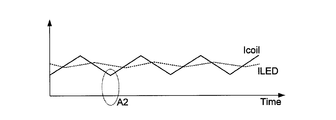
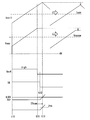
- FIG. 4 is a diagram illustrating an example of waveforms of a coil current and an LED current in a CCM mode. 5 is a timing chart for explaining an LED current correction function in a QR mode.
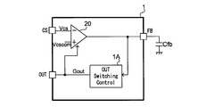
- FIG. 2 is a diagram in which only a configuration related to current feedback control in a CCM mode in the light emitting element driving device illustrated in FIG. 1 is extracted.
- FIG. 4 is a diagram illustrating a light emitting element driving device equipped with an LED current correction function in a CCM mode.
- FIG. 6 is a timing chart showing an example of various signal waveforms in the CCM mode in the configuration shown in FIG. 5 (FIG. 1).
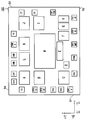
- 7 is a timing chart showing an example of various signal waveforms in a CCM mode in the configuration shown in FIG. It is the figure which looked at the light emitting element drive concerning one embodiment as an IC package product from the upper surface.
- FIG. 2 is a plan view showing an arrangement configuration of a chip provided in the light emitting element driving device according to one embodiment. It is a figure showing the example of composition of a liquid crystal display.
- FIG. 1 is a circuit diagram showing an overall configuration of a light emitting element driving device according to one embodiment of the present invention.
- the light emitting element driving device 1 illustrated in FIG. 1 is a device that drives an LED array 50 configured by connecting a plurality of LEDs in series. That is, the light emitting element driving device 1 is a device that drives an LED as an example of a light emitting element to be driven.
- the light emitting element to be driven is not limited to the LED.
- the light emitting element driving device 1 can operate by switching between a QR mode (quasi-resonant: quasi-resonant system) and a CCM mode (continuous current mode: continuous current method). ing. That is, both modes are mounted on one IC. Details of both modes will be described later.
- the light emitting element driving device 1 includes an internal voltage generation unit 11, an IC power supply UVLO unit 12, a UVLO unit 13, an internal voltage UVLO unit 14, a low-pass filter 15, an amplifier 16, an ODP (Over Duty Protection) unit 17, comparison voltage generation unit 18, comparator 19, error amplifier 20, comparator 21, oscillator 22, abnormality detection unit 23, and control logic unit 24 It is a semiconductor IC configured by integrating parts.
- a drive control unit includes the comparator 19, the error amplifier 20, the comparator 21, the oscillator 22, the control logic unit 24, the driver Dr1, and the comparator CP2.
- the drive control unit generates a gate output signal Gout (drive signal) output from the OUT terminal.
- the light-emitting element driving device 1 includes a VCC terminal, an ULVO terminal, a SEL terminal, a REG90 terminal, a QRCOMP terminal, a PWM terminal, a DUTYON terminal, an ADIM terminal, and an RT terminal as external terminals for establishing an electrical connection with the outside.
- FAILB terminal, ZT terminal, OUT terminal, CS terminal, FB terminal, DGND terminal, and GND terminal as external terminals for establishing an electrical connection with the outside.
- voltage dividing resistors R1, R2, a diode D1, a capacitor C1, a coil L1, an LED array 50, a capacitor C2, a voltage dividing resistor R11, R12, a switching element M1, a gate resistor Rg, a current detection resistor Rs, a feedback capacitor Cfb, a capacitor C11, and a resistor R21 are arranged.
- the LED array 50 is a light emitting unit configured by connecting a plurality of LEDs in series.
- an LED array may be configured by connecting LEDs in series and parallel, or a single LED may be used instead of the LED array.
- the input voltage Vin is applied to the high potential side end (anode) of the LED array 50.
- One end of the coil L1 is connected to a low potential side end (cathode) of the LED array 50.
- the other end of the coil L1 is connected to an anode of a reflux diode D1.
- the high potential side end of the LED array 50 is connected to the cathode of the diode D1.
- a capacitor C1 is connected in parallel between both ends of the LED array 50.
- the capacitor C1 averages a coil current Icoil, which is a current flowing through the coil L1, to obtain an LED current ILED, which is a current flowing through the LED array 50.
- the other end of the coil L1 is connected to a drain of a switching element M1 composed of, for example, an n-channel MOSFET.
- the source of the switching element M1 is connected to a ground potential application terminal via a current detection resistor Rs.
- the voltage after the input voltage Vin is divided by the voltage dividing resistors R1 and R2 is applied to the UVLO (Under Voltage Lock Out) terminal.
- the UVLO unit 13 causes the control logic unit 24 to keep the switching element M1 off and stop switching. That is, the UVLO terminal is a terminal for UVLO of the application power supply.
- the power supply voltage Vcc is applied to the VCC terminal. That is, the VCC terminal is a power supply terminal for the IC.
- the IC power supply UVLO unit 12 causes the control logic unit 24 to shut down the IC.
- the internal voltage generator 11 generates the internal voltage Vreg based on the power supply voltage Vcc.
- the generated internal voltage Vreg can be output from the REG90 terminal to the outside.
- the REG90 terminal is a 9.0 V output terminal.
- the output voltage value here is an example.
- An external capacitor C11 is connected to the REG90 terminal.
- the capacitor C11 is preferably a ceramic capacitor.
- the internal voltage UVLO unit 14 causes the control logic unit 24 to shut down the IC.
- the control logic unit 24 outputs the gate output signal Gout from the OUT terminal to the outside using the driver Dr1.
- the gate output signal Gout is a pulse signal composed of High and Low.
- the OUT terminal is connected to the gate (control terminal) of the switching element M1 via a gate resistor Rg, which is an external component.
- the gate output signal Gout is applied as a gate signal Gt to the gate of the switching element M1 via the gate resistor Rg.
- the switching element M1 is turned on / off by the gate output signal Gout.
- a pulse-like PWM dimming signal is input from the outside to the PWM terminal.
- the ODP unit 17 switches whether to activate the PWM on-time limiting function according to an on-off setting signal input from the outside via the DUTYON terminal. For example, when the on / off setting signal is Low, the on time of the PWM dimming signal is limited, and when the on / off setting signal is High, the PWM on time limiting function is turned off.
- the control logic unit 24 outputs the gate output signal Gout for turning on and off from the OUT terminal while the PWM dimming signal output from the ODP unit 17 is High, and keeps the gate output signal Gout Low during the Low period. Thereby, the dimming of the LED array 50 can be performed by adjusting the on-duty of the PWM dimming signal.
- the SEL terminal is a terminal to which a selection input signal for selecting whether to operate the light emitting element driving device 1 in the QR mode or the CCM mode is input.
- the SEL terminal is pulled down by a pull-down resistor Rp inside the IC.
- the connection node between the SEL terminal and the pull-down resistor Rp is connected to the non-inverting input terminal of the comparator CP1.
- a predetermined reference voltage is applied to the inverting input terminal of the comparator CP1.
- the comparator CP1 In response to the selection input signal being High or Low, the comparator CP1 outputs a High or Low selection signal SEL_sig.
- the control logic unit 24 selects the QR mode or the CCM mode according to the level of the input selection signal SEL_sig. For example, when the selection input signal is high, the QR mode is selected, and when the selection input signal is low, the CCM mode is selected.
- the CS terminal and the comparator 19 are used for current detection in the QR mode.
- the CS terminal is connected to a connection node between the switching element M1 and the current detection resistor Rs.
- the non-inverting input terminal of the comparator 19 receives, via a terminal CS, a current detection signal Vcs after the coil current Icoil has been subjected to current / voltage conversion by the current detection resistor Rs.
- the current detection threshold voltage Vcsqr output from the comparison voltage generator 18 is input to the inverting input terminal of the comparator 19.
- the comparator 19 outputs a comparison result between the current detection signal Vcs and the current detection threshold voltage Vcsqr to the control logic unit 24.
- the ADIM terminal is an external terminal for inputting an analog dimming signal (analog voltage signal) from outside.
- the comparison voltage generator 18 outputs a current detection threshold voltage Vcsqr obtained by multiplying the analog dimming signal by the first gain magnification.
- the dimming of the LED array 50 in the QR mode can be performed by adjusting the analog dimming signal.
- the CS terminal and the error amplifier 20 are used for current feedback control in the CCM mode.
- the current detection signal Vcs is input to the inverting input terminal of the error amplifier 20 via the CS terminal.
- a current feedback voltage Vcsccm as a reference voltage output from the comparison voltage generation unit 18 is input to a non-inverting input terminal of the error amplifier 20.
- An FB terminal is connected to the output terminal of the error amplifier 20.
- An external capacitor Cfb is connected to the FB terminal.
- the comparison voltage generator 18 When the CCM mode is selected by the selection signal SEL_sig, the comparison voltage generator 18 outputs a current feedback voltage Vcsccm obtained by multiplying the analog dimming signal by the second gain magnification.
- the dimming of the LED array 50 in the CCM mode can be performed by adjusting the analog dimming signal.
- comparison voltage generator 18 The operation of the comparison voltage generator 18 will be described later in more detail.
- the output terminal of the error amplifier 20 is connected to the non-inverting input terminal of the comparator 21.
- An oscillation signal output from the oscillator 22 is input to an inverting input terminal of the comparator 21.
- the oscillation signal has, for example, a sawtooth waveform.
- the comparator 21 outputs a PWM signal Spwm to the control logic unit 24 as a comparison result between the output of the error amplifier 20 and the oscillation signal.
- the frequency of the PWM control is fixed, but this frequency is set by an external resistor R21 connected to the RT terminal.
- the ZT terminal is a terminal for detecting a zero cross of the coil current Icoil in the QR mode, and is connected to a connection node between the voltage dividing resistors R11 and R12.
- the inverting input terminal of the comparator CP2 is connected to the ZT terminal.
- a predetermined reference voltage is applied to a non-inverting input terminal of the comparator CP2.
- the comparator CP2 outputs the zero-cross detection signal to the control logic unit 24.
- the comparator CP3 is also connected to the ZT terminal, but the comparator CP3 is used for correction control of the LED current ILED in the QR mode, and details thereof will be described later.
- the amplifier 16 amplifies and outputs the output from the low-pass filter 15.
- the control logic unit 24 outputs the gate output signal Gout of the OUT terminal to the low-pass filter 15 when the PWM dimming signal is High.
- the low-pass filter 15 smoothes the gate output signal Gout and outputs it. That is, the QRCOMP terminal outputs a DC voltage proportional to the on-duty of the gate output signal Gout to the outside when the QR mode is selected by the selection signal SEL_sig and when the PWM dimming signal is High.
- the DC voltage output from the QRCOMP terminal is used to generate an analog dimming signal input to the ADIM terminal, and corrects the linearity of the LED current in the QR mode.
- the control logic unit 24 When the control logic unit 24 detects an abnormality, the control logic unit 24 outputs an abnormality signal indicating an abnormal state from the FAILB terminal to the outside by using the abnormality detection unit 23. Note that the abnormal signal has a different level depending on the abnormal state or the normal state.
- the GND terminal is a terminal for grounding the IC.
- the DGND terminal is a terminal for taking digital ground of the IC.
- QR mode and CCM mode Next, each operation in the QR mode and the CCM mode will be described.
- the control logic unit 24 controls the operation in the QR mode by the selection signal SEL_sig indicating the selection.
- the control logic unit 24 first outputs a High gate output signal Gout from the OUT terminal to turn on the switching element M1. Then, the coil current Icoil starts to flow through the turned-on switching element M1 and the current detection resistor Rs and increases. At this time, the current detection signal Vcs detected by the current detection resistor Rs increases. When the current detection signal Vcs becomes equal to or higher than the current detection threshold voltage Vcsqr, the output of the comparator 19 rises to High, and the control logic unit 24 falls the gate output signal Gout to Low.
- the switching element M1 is turned off, the drain voltage Vrd of the switching element M1 increases, and the coil current Icoil starts flowing through the diode D1 and decreases.
- the ZT voltage Vzt applied to the ZT terminal increases as the drain voltage Vdr increases, and then gradually decreases.
- the drain voltage Vdr drops sharply, and the ZT voltage Vzt also drops sharply.
- the output of the comparator CP2 rises to High.
- the control logic unit 24 raises the gate output signal Gout to High, and turns on the switching element M1 again.
- FIG. 2 shows an example of the waveform of the coil current Icoil and the LED current ILED in such a QR mode.
- the coil current Icoil After increasing from zero, the coil current Icoil starts decreasing at a predetermined current value and increases again when reaching zero.
- the QR mode soft switching is performed so that no current flows through the switching element M1 when the switching element M1 is turned on, so that generation of heat (loss) and noise are suppressed.
- the ripple of the LED current ILED obtained by averaging the coil current Icoil increases.
- the control logic unit 24 controls the operation of the CCM mode.
- the error amplifier 20 and the comparator 21 are enabled, and in response to the PWM signal Spwm output from the comparator 21, the control logic unit 24 outputs a gate output signal Gout consisting of High and Low, and controls the switching element M1 to turn on and off. I do. That is, current feedback control is performed in which the on-duty of the PWM signal Spwm is adjusted such that the average value of the current detection signal Vcs matches the current feedback voltage Vcsccm. Thereby, control is performed so that the average value of the coil current Icoil matches the desired value.
- FIG. 3 shows an example of waveforms of the coil current Icoil and the LED current ILED in such a CCM mode.
- the switching element M1 is turned on and off in response to the PWM signal Spwm, and the coil current Icoil repeats increase and decrease.
- the coil current Icoil is controlled in a constantly flowing state.
- the switching cycle of the switching element M1 is fixed. At this time, since the amplitude of the coil current Icoil is small, the ripple of the LED current ILED is small.
- a region A2 in FIG. 3 when the switching element M1 is turned on, hard switching in which a current flows through the switching element M1 is performed, which is disadvantageous in terms of heat generation (loss) and generation of noise.
- the QR mode and the CCM mode can be selected by the selection input signal with one IC, so that the degree of freedom in design is improved. Note that it is also possible to switch to the operation of the other mode while one of the modes is operating. Thereby, for example, when switching the brightness of the LED from low brightness to high brightness, it is possible to switch from the QR mode to the CCM mode in which the ripple of the LED current is small.
- the current detection threshold voltage Vcsqr is basically set by the following equation (1).
- Vcsqr Vadim ⁇ G1 (1)
- Vadim is an analog dimming signal
- G1 is a first gain magnification.
- Vcsccm Vadim ⁇ G2 (2)
- Vadim is an analog dimming signal
- G2 is a second gain magnification.
- the current detection threshold voltage Vcsqr and the current feedback voltage Vcsccm are set as follows according to the ON / OFF of the function of the ODP unit 17 by setting the ON / OFF setting signal input to the DUTYON terminal. .
- Vcsqr Vadim ⁇ G1 (Vadim ⁇ Vclp1) (11)
- Vcsqr Vclp1 ⁇ G1 (Vadim> Vclp1)
- Vcsqr Vadim ⁇ G1 (Vadim ⁇ Vclp2)
- Vcsqr Vclp2 ⁇ G1 (Vadim> Vclp2)
- Vclp1 and Vclp2 are clamp voltages of the analog dimming signal Vadim, and Vclp1> Vclp2.
- the current detection threshold voltage Vcsqr and the current feedback voltage Vcsccm can be limited by the clamp voltages Vclp1 and Vclp2.
- Vclp1 used when the function of the ODP unit 17 is on is higher than Vclp2 used when the function is off is that the ON time of the PWM dimming signal is limited when the function is on. This is because there is no problem even if the restrictions on the voltage Vcsqr and the current feedback voltage Vcsccm are relaxed.
- the light emitting element driving device 1 of the present embodiment has a function of correcting the LED current ILED (coil current Icoil) in the QR mode to increase the accuracy.
- ILED coil current Icoil
- the gate output signal Gout output from the control logic unit 24 falls to Low.
- the gate signal Gt decreases to a timing t3 with a certain slope.
- the drain voltage Vdr starts to increase due to the turning off of the switching element M1, and at timing t4, the drain voltage Vdr reaches the LED voltage VLED.
- the coil current Icoil changes from increasing to decreasing.
- the coil current Icoil is increased as an accumulation of the delay from the timing t1 to t2 by the internal circuit, the delay from the timing t2 to t3 by the external components, and the delay from the timing t3 to t4 due to the rise of the drain voltage Vdr.
- a delay in the return timing that starts decreasing decreases by the delay time DTqr.
- the increase in the coil current Icoil is maintained only during the delay time DTqr. Therefore, the LED current ILED obtained by averaging the coil current Icoil is shifted to a higher value, and a problem occurs in current accuracy.
- control is performed using the ZT voltage Vzt generated at the ZT terminal.
- the ZT voltage Vzt As shown in FIG. 4, as the drain voltage Vdr increases from the timing t3, the ZT voltage Vzt also increases, and at a timing t4, the ZT voltage Vzt reaches a predetermined threshold voltage ZTH1.
- the threshold voltage ZTH1 is set as a reference voltage of the comparator CP3, and the output of the comparator CP3 rises at a timing t4. Therefore, in the present embodiment, the control logic unit 24 starts counting from the timing t1 when the output signal CS_DET of the comparator 19 rises and counts until the timing t4 when the output of the comparator CP3 becomes High, thereby detecting the delay time DTqr. I do.
- the control logic unit 24 adjusts the analog dimming signal Adim according to the delay time DTqr. As a result, the current detection threshold voltage Vcsqr is adjusted, so that the coil current Icoil and thus the LED current ILED can be corrected. In addition to the method of feeding back the analog dimming signal Adim as described above, the control logic unit 24 may adjust the on-duty of the gate output signal Gout. That is, the control logic unit 24 corresponds to an example of a coil current correction unit.
- the delay time DTqr can be detected using the ZT voltage Vzt of the ZT terminal used for zero-cross detection in the QR mode.
- the drain voltage Vdr sharply decreases, and the ZT voltage Vzt also decreases.
- the output of the comparator CP2 rises to High, and a zero cross of the coil current Icoil is detected. That is, the threshold voltage ZTH2 is set as the reference voltage of the comparator CP2.
- ZTH2 is set to a value close to zero, and ZTH1 is higher than ZTH2 and has a different voltage level from ZTH2. Therefore, in this embodiment, both the comparator CP2 and the comparator CP3 are provided. By providing the comparator CP3 for comparison with ZTH1, the delay time DTqr can be accurately detected. However, the comparator CP2 for zero-cross detection can also be used for detecting the delay time DTqr. In that case, the number of parts can be reduced.
- LED Current Correction in CCM Mode Further, in the light emitting element driving device of the present embodiment, it is possible to mount a function of correcting the LED current ILED (coil current Icoil) in the CCM mode to increase the accuracy, and this function will be described here. .
- FIG. 5 is a diagram in which only the configuration related to the current feedback control in the CCM mode in the light emitting element driving device 1 shown in FIG. 1 is extracted.
- the switching control unit 1A shown in FIG. 5 is a functional unit including a comparator 21, an oscillator 22, a control logic unit 24, and a driver Dr1, and outputs a gate output signal Gout to an OUT terminal based on an output from the error amplifier 20. Output from The configuration shown in FIG. 5 does not have a function of correcting the LED current in the CCM mode.
- the switching control section 1A adjusts the on-duty of the gate output signal Gout such that the average value of the current detection signal Vcs matches the current feedback voltage Vcsccm.
- FIG. 7 is a timing chart showing an example of various signal waveforms in the CCM mode in the configuration shown in FIG. 5 (FIG. 1).
- the gate output signal Gout is High, the coil current Icoil starts to increase by turning on the switching element M1, and the current detection signal Vcs rises sharply from 0V and then rises.
- the gate output signal Gout is switched to Low at timing t11 by adjusting the on-duty. Due to the presence of the external gate resistance Rg and the gate capacitance (not shown), the gate signal Gt switches to Low at the delayed timing t12.
- the drain voltage Vdr increases from timing t12, and at timing t13, the drain voltage Vdr reaches the LED voltage VLED. At this timing t13, the coil current Icoil changes from increasing to decreasing.
- the error amplifier 20 monitors the current detection signal Vcs only during the period when the gate output signal Gout is High. Thereby, as shown in FIG. 7, the on-duty of the gate output signal Gout is adjusted so that the average value of the current detection signal Vcs matches the current feedback voltage Vcsccm.
- the coil current Icoil continues to increase only for the delay time DTccm, and the average value of the coil current Icoil is shifted to be higher than the desired value Iccm. Therefore, a problem arises in the accuracy of the LED current ILED. That is, even if it is intended that the IC (light emitting element driving device) can be accurately controlled, the LED current ILED actually shifts.
- the light emitting element driving device 100 shown in FIG. 6 is obtained by partially modifying the configuration of the light emitting element driving device 1 shown in FIG. 5 (FIG. 1).
- sample and hold unit 100A is inserted between the CS terminal and the inverting input terminal of the error amplifier 20.
- the ZT voltage Vzt at the ZT terminal is also used.
- the error amplifier 20 monitors the sampling output Vsmp output from the sample and hold unit 100A.
- the sample and hold unit 100A, the error amplifier 20, and the switching control unit 1A constitute an example of a drive control unit or a coil current correction unit.
- FIG. 8 is a timing chart showing an example of various signal waveforms in the CCM mode in the configuration shown in FIG. During the period in which the gate output signal Gout is High during the timing t10 to t11 shown in FIG. 8, the sample and hold unit 100A outputs the current detection signal Vcs as it is as the sampling output Vsmp.
- the sample-and-hold unit 100A performs a hold operation to maintain the sampling output Vsmp at that timing.
- the drain voltage Vdr starts to increase, and accordingly, the ZT voltage Vzt of the ZT terminal also increases.
- the ZT voltage Vzt reaches the threshold voltage Zth.
- the error amplifier 20 monitors the sampling output Vsmp only during a period from when the gate output signal Gout switches to High to when the ZT voltage Vzt reaches the threshold voltage Zth.
- the on-duty of the gate output signal Gout is adjusted so that the average value of the sampling output Vsmp matches the current feedback voltage Vcsccm.
- the average value of the sampling output Vsmp is corrected to be higher.
- the sampling output Vsmp and the coil current Icoil are corrected to be lower. Therefore, the LED current ILED is corrected so as to approach the desired value, and the current accuracy can be improved.
- a method similar to the above-described method in the QR mode can be applied to the CCM mode. That is, the control logic unit 24 starts counting from the timing t11 when the gate output signal Gout shown in FIG. 8 switches from High to Low, and counts up to the timing t13 when the ZT voltage Vzt reaches the threshold voltage Zth, so that the delay time is increased. DTccm is detected.
- a comparator for comparing the ZT voltage Vzt with the threshold voltage Zth may be provided in the configuration of FIG. Then, the control logic unit 24 adjusts the analog dimming signal Adim according to the detected delay time DTccm.
- control logic unit 24 may adjust the on-duty of the gate output signal Gout.
- a modified embodiment in which control is performed using a comparator in the CCM mode as in the QR mode is also possible, in which case the error amplifier 20 and the FB terminal are unnecessary.
- the control logic unit 24 starts time measurement from the timing when the gate output signal Gout is switched from Low to High to turn on the switching element M1. Then, the control logic unit 24 monitors the output of the comparator to which the reference voltage and the current detection signal Vs are input, and ends the time measurement at the timing when the current detection signal Vs becomes equal to or higher than the reference voltage.
- the gate output signal Gout is switched from High to Low at a timing when a time equal to the measurement time from the start to the end of the time measurement has elapsed. As a result, the average value of the coil current Icoil can be controlled to a desired current value defined by the reference voltage.
- control logic unit 24 detects a difference between the current detection signal Vs when the switching element M1 is turned on and the reference voltage, and adds the detected difference to the reference voltage. Using the determined voltage as the current detection threshold voltage as in the QR mode, the output of the comparator is monitored to determine the timing of switching the gate output signal Gout from High to Low. As a result, the average value of the coil current Icoil can be controlled to a desired current value defined by the reference voltage.
- control logic unit 24 detects the delay time DTccm, and adjusts the reference voltage or the ON time according to the detected delay time Dtccm. Then, the coil current Icoil can be corrected.
- FIG. 9 is a top view of the light emitting element driving device 1 (or 100) according to the present embodiment as an IC package product.
- FIG. 9 shows the arrangement (pin arrangement) of each external terminal.
- the IC package shown in FIG. 9 is configured as an SOP (Small Outline Package).
- the lead frame as each external terminal is connected to an electrode of the LSI chip by a bonding wire (Au wire or the like), and the LSI chip and the lead frame are sealed with a sealing material (epoxy resin or the like).
- the IC package has a rectangular sealing material when viewed from above.
- the sealing material has a first side that is one long side, and a second side that is a long side facing and parallel to the first side.
- a VCC terminal, a UVLO terminal, a SEL terminal, a PWM terminal, a QRCOMP terminal, an ADIM terminal, a FAILB terminal, and a DUTYON terminal are arranged in order.
- a REG90 terminal, a CS terminal, an OUT terminal, a GND terminal, a DGND terminal, an FB terminal, a ZT terminal, and an RT terminal are sequentially arranged.
- the VCC terminal and UVLO terminal of the input power supply system, the SEL terminal, the PWM terminal, the QRCOMP terminal, the ADIM terminal, the FAILB terminal, and the DUTYON terminal which are the input / output relationship with the microcomputer (not shown), and the IC package is a PCB (board). In consideration of the wiring at the time of mounting, they are arranged collectively on the same long side.
- the FB terminal is arranged between the DGND terminal and the ZT terminal. If a high voltage is applied to the FB terminal, the on-duty of the PWM control becomes very large in the CCR mode, and the LED current may be overcurrent. However, even if the FB terminal is short-circuited with the adjacent DGND terminal or ZT terminal, the DGND terminal and the ZT terminal are terminals to which a low voltage is applied, and there is no problem because the low voltage is applied to the FB terminal.
- FIG. 10 is a plan view showing the arrangement of the electrode pads and the arrangement of the regions where the components shown in FIG. 1 are arranged in the chip 101 provided in the light emitting element driving device 1 according to the present embodiment.
- the X-axis direction and the Y-axis direction orthogonal to the X-axis direction are shown.
- the X-axis direction is more specifically shown in the X1 direction and the X2 direction, and the Y-axis direction is more specific.
- the Y1 and Y2 directions In the Y1 and Y2 directions.
- the X2 direction and the Y2 direction are directions approaching each other.
- the chip 101 shown in FIG. 10 has a rectangular outer shape.
- the rectangular shape has a first side S1 extending in the Y-axis direction on the X2 direction side, a second side S2 extending in the X-axis direction on the Y2 direction side, a third side S3 extending in the Y-axis direction on the X1 direction side, A fourth side S4 extending in the X-axis direction on the Y1 direction side.
- the chip 101 has two VCC pads, UVLO pads, SEL pads, PWM pads, QRCOMP pads, ADIM pads, FAILB pads, DUTYON pads, RT pads, ZT pads, FB pads, DGND pads, and two GND pads as electrode pads. , Two OUT pads, a CS pad, and two REG90 pads. Each of these pads is provided corresponding to each terminal of the IC package shown in FIG.
- CSAlong the first side S1, the CS pad, the first REG90 pad, the second REG90 pad, the first VCC pad, the second VCC pad, and the UVLO pad are arranged in this order in the Y2 direction.
- a SEL pad, a PWM pad, a QRCOMP pad, an ADIM pad, and a FAILB pad are arranged in this order in the X1 direction.
- a DUTYON pad, an RT pad, and a ZT pad are arranged in this order in the Y1 direction.
- an FB pad, a DGND pad, a first GND pad, a second GND pad, a first OUT pad, and a second OUT pad are arranged in this order in the X2 direction.
- the chip 101 has areas A to M as areas where the components shown in FIG. 1 are arranged.
- a region, B region, and C region are arranged in this order in the Y2 direction when viewed in the X1 direction.
- the A region overlaps the first OUT pad and the second OUT pad in the X-axis direction when viewed in the Y2 direction, and overlaps the CS pad in the Y-axis direction when viewed in the X1 direction.
- the B region overlaps the A region in the X-axis direction when viewed in the Y2 direction, and overlaps the first REG90 pad and the second REG90 pad in the Y-axis direction when viewed in the X1 direction.
- the B region does not overlap the first VCC pad in the Y-axis direction when viewed in the X1 direction.
- the first VCC pad and the second VCC pad are connected to the input terminal of the internal voltage generator 11 arranged in the region B via the top metal wiring.
- Internal voltage generator 11 includes a power transistor.
- the output terminal of the internal voltage generator 11 is connected to the power input terminal of the driver Dr1 arranged in the region A via the top metal wiring.
- Driver Dr1 includes a power transistor.
- the internal voltage Vreg generated by the internal voltage generator 11 based on the power supply voltage Vcc applied to the first VCC pad and the second VCC pad is supplied as the power supply voltage of the driver Dr1.
- the output terminal of the driver Dr1 is connected to the first OUT pad and the second OUT pad.
- a region does not overlap the first GND pad and the second GND pad in the X-axis direction when viewed in the Y2 direction.
- the ground end of the driver Dr1 is connected to the first GND pad and the second GND pad.
- first and second REG90 pads and the first and second VCC pads are arranged near the B region, and the A region is arranged near the first and second OUT pads and the first and second GND pads. .
- the C region does not overlap with the first VCC pad in the Y-axis direction when viewed in the X1 direction, but overlaps with the second VCC pad and the UVLO pad in the Y-axis direction when viewed in the X1 direction.
- the area C overlaps the area B in the X-axis direction when viewed in the Y2 direction.
- UVLO section 13 is arranged in region C.
- the C area to the H area are arranged in this order in the X1 direction when viewed in the Y1 direction.
- the D region is shifted from the SEL pad in the X1 direction when viewed in the Y1 direction, and does not overlap with the SEL pad in the X-axis direction.
- the D area overlaps the C area in the Y axis direction when viewed in the X2 direction. Thereby, the D region is arranged near the SEL pad.
- the comparator CP1 is arranged in the D area.
- the E region overlaps the PWM pad and the QRCOMP pad in the X-axis direction when viewed in the Y1 direction.
- the E region overlaps the C region in the Y axis direction when viewed in the X2 direction, but does not overlap the D region in the Y axis direction.
- the ODP unit 17 is arranged in the area E.
- the distance in the Y-axis direction between the PWM pad and the E region when viewed in the X2 direction is shorter than the distance in the X-axis direction between the DUTYON pad and the E region when viewed in the Y1 direction.
- the ON / OFF setting signal applied to the DUTYON pad is constant at the High level or the Low level, and the tolerance of noise to the signal applied to the DUTYON pad is Is large.
- the F region is shifted from the QRCOMP pad in the X1 direction when viewed in the Y1 direction, does not overlap with the QRCOMP pad in the X-axis direction, and overlaps with the ADIM pad in the X-axis direction.
- the F region overlaps the D region and the E region in the Y axis direction when viewed in the X2 direction.
- Amplifier 16 is arranged in the F region.
- the F region is located near the QRCOMP pad.
- the G area overlaps the ADIM pad in the X axis direction when viewed in the Y1 direction, and overlaps the F area in the Y axis direction when viewed in the X2 direction.
- the comparison voltage generator 18 is arranged in the G area.
- the G region is located near the ADIM pad. Since an analog dimming signal, which is an analog voltage, is applied to the ADIM pad, noise is suppressed and influence on dimming is suppressed.
- the H region overlaps the FAILB pad in the X-axis direction when viewed in the Y1 direction, and overlaps the G region in the Y-axis direction when viewed in the X2 direction.
- the abnormality detection unit 23 is arranged in the H area. The H region is located near the FAILB pad.
- a set of G and H areas, an I area and a J area are arranged in this order in the Y1 direction when viewed in the X2 direction.
- the I region is shifted from the DUTYON pad in the Y1 direction when viewed in the X2 direction, and does not overlap the DUTYON pad in the Y-axis direction, but overlaps the RT pad in the Y-axis direction.
- Oscillator 22 is arranged in region I. The I region is located near the RT pad.
- the J area is shifted from the RT pad to the Y1 direction side in the X2 direction, and does not overlap the RT pad in the Y-axis direction, but overlaps the ZT pad in the Y-axis direction.
- the comparators CP2 and CP3 are arranged in the J area.
- the J region is located near the ZT pad.
- the J area, the K area, the L area, and the A area are arranged in this order in the X2 direction when viewed in the Y2 direction.
- the K region is shifted from the FB pad to the X2 direction side when viewed in the Y2 direction, and does not overlap with the FB pad in the X-axis direction, but overlaps with the DGND pad in the X-axis direction.
- the K region overlaps the J region in the Y axis direction when viewed in the X2 direction.
- the error amplifier 20 is arranged in the K area.
- the K region is located near the FB pad.
- the L region overlaps the first and second GND pads in the X-axis direction when viewed in the Y2 direction.
- the L region overlaps the K region in the Y axis direction when viewed in the X2 direction.
- the comparator 19 is arranged in the L region.
- An M region is arranged at the center of the chip 101 surrounded by the A region to the L region.
- the control logic unit 24 is arranged in the M area.
- FIG. 11 shows a configuration example of a liquid crystal display device.
- the configuration shown in FIG. 11 is of a so-called edge light type, and is not limited thereto, and may be of a direct type.
- the liquid crystal display device X shown in FIG. 11 includes a backlight 81 and a liquid crystal panel 82.
- the backlight 81 is an illumination device (an example of a light emitting device) that illuminates the liquid crystal panel 82 from the back.
- the backlight 81 has an LED light source section 811, a light guide plate 812, a reflection plate 813, and optical sheets 814.
- the LED light source unit 811 includes an LED and a substrate on which the LED is mounted, and the light emitting element driving device for driving the LED according to the above-described embodiment can be applied.
- Light emitted from the LED light source unit 811 enters inside from the side surface of the light guide plate 812.
- a light guide plate 812 made of an acrylic plate guides light entering inside to the entire inside while totally reflecting the light, and emits the light as planar light from the surface on which the optical sheets 814 are arranged.
- the reflection plate 813 reflects the light leaked from the light guide plate 812 and returns the light to the inside of the light guide plate 812.
- the optical sheets 814 are made of a diffusion sheet, a lens sheet, or the like, and aim at uniforming the luminance of light illuminating the liquid crystal panel 82, improving the luminance, and the like.
- the light emitting element driving device may have only one of the QR mode and the CCM mode.
- the capacitor C1 for averaging the coil current Icoil may not be necessarily provided. Note that a configuration without the capacitor C1 can be adopted even when both the QR mode and the CCM mode are provided.
- the present invention can be used, for example, in a light emitting element driving device that drives an LED.
Landscapes
- Circuit Arrangement For Electric Light Sources In General (AREA)
- Led Devices (AREA)
- Dc-Dc Converters (AREA)
Abstract
スイッチング素子の制御端子と接続される第1外部端子と、前記スイッチング素子をオンオフ駆動する駆動信号を生成して前記第1外部端子から出力する駆動制御部と、を備え、前記駆動制御部は、コイルを流れるコイル電流が増加から減少へ転じる折り返しタイミングの遅延に基づいて前記駆動信号を調整することで前記コイル電流を補正するコイル電流補正部を有する発光素子駆動装置である。
Description
本発明は、発光素子駆動装置に関する。
従来、LED(発光ダイオード)に代表される発光素子を駆動する発光素子駆動装置が種々に提案されている。発光素子の一例であるLEDを駆動する従来の発光素子駆動装置の外部においては、LEDを複数直列接続して構成したLEDアレイの低電位側端(カソード)に対してコイルとスイッチング素子が順に直列に接続され、LEDアレイの両端間にコンデンサが並列接続され、コンデンサとコイルとの接続構成の両端間に還流用のダイオードが接続される。
上記スイッチング素子がオンオフ制御されることで、LEDアレイに流れるLED電流が制御される。スイッチング素子がオンとされると、上記コイルに流れる電流が増加し、スイッチング素子がオフとされると、上記コイルおよび上記ダイオードに流れる電流は減少する。上記コンデンサは、コイルに流れる電流を平均化してLED電流とする。
なお、このような従来の発光素子駆動装置の一例は、特許文献1に開示されている。
上記従来の発光素子駆動装置では、スイッチング素子がオンの状態からオフになるときにコイルに流れる電流(コイル電流)は増加から減少へ転じる。しかしながら、例えば発光素子駆動装置の出力端子とスイッチング素子の制御端子との間に接続される外付けの抵抗部品等による上記制御端子に印加される制御電圧のオフレベルへの切替えの遅れ等に起因して、コイル電流が増加から減少へ転じる折り返しタイミングが遅延する虞があった。この場合、その遅延分、コイル電流の増加が継続され、コイル電流を平均化したLED電流の値が所望値よりも高くなり、精度としての問題が生じる。
上記問題点に鑑み、本発明は、発光素子に流れる電流の精度を向上させることができる発光素子駆動装置を提供することを目的とする。
上記目的を達成するために本発明は、少なくとも一つの発光素子からなり、一端に入力電圧が印加される発光部と、
前記発光部の他端に一端が接続されるコイルと、
前記コイルの他端と前記発光部の一端との間に接続されるダイオードと、
前記コイルの他端に接続される第1端子を有するスイッチング素子と、
を含む外部構成における前記発光部を駆動する発光素子駆動装置であって、
前記スイッチング素子の制御端子と接続される第1外部端子と、
前記スイッチング素子をオンオフ駆動する駆動信号を生成して前記第1外部端子から出力する駆動制御部と、
を備え、
前記駆動制御部は、前記コイルを流れるコイル電流が増加から減少へ転じる折り返しタイミングの遅延に基づいて前記駆動信号を調整することで前記コイル電流を補正するコイル電流補正部を有する構成としている。
前記発光部の他端に一端が接続されるコイルと、
前記コイルの他端と前記発光部の一端との間に接続されるダイオードと、
前記コイルの他端に接続される第1端子を有するスイッチング素子と、
を含む外部構成における前記発光部を駆動する発光素子駆動装置であって、
前記スイッチング素子の制御端子と接続される第1外部端子と、
前記スイッチング素子をオンオフ駆動する駆動信号を生成して前記第1外部端子から出力する駆動制御部と、
を備え、
前記駆動制御部は、前記コイルを流れるコイル電流が増加から減少へ転じる折り返しタイミングの遅延に基づいて前記駆動信号を調整することで前記コイル電流を補正するコイル電流補正部を有する構成としている。
また、本発明の別態様は、少なくとも一つの発光素子からなり、一端に入力電圧が印加される発光部と、
前記発光部の他端に一端が接続されるコイルと、
前記コイルの他端と前記発光部の一端との間に接続されるダイオードと、
前記コイルの他端に接続される第1端子を有するスイッチング素子と、
を含む外部構成における前記発光部を駆動する発光素子駆動装置であって、
前記スイッチング素子の制御端子と接続される第1外部端子と、
前記スイッチング素子をオンオフ駆動する駆動信号を生成して前記第1外部端子から出力する駆動制御部と、
選択入力信号が入力される第2外部端子と、
を備え、
前記駆動制御部は、前記選択入力信号に応じてQRモード(quasi-resonant:擬似共振方式)と、CCMモード(continuous current mode:電流連続方式)と、を切替えて動作する構成としている。
前記発光部の他端に一端が接続されるコイルと、
前記コイルの他端と前記発光部の一端との間に接続されるダイオードと、
前記コイルの他端に接続される第1端子を有するスイッチング素子と、
を含む外部構成における前記発光部を駆動する発光素子駆動装置であって、
前記スイッチング素子の制御端子と接続される第1外部端子と、
前記スイッチング素子をオンオフ駆動する駆動信号を生成して前記第1外部端子から出力する駆動制御部と、
選択入力信号が入力される第2外部端子と、
を備え、
前記駆動制御部は、前記選択入力信号に応じてQRモード(quasi-resonant:擬似共振方式)と、CCMモード(continuous current mode:電流連続方式)と、を切替えて動作する構成としている。
本発明の発光素子駆動装置によれば、発光素子に流れる電流の精度を向上させることができる。
以下に本発明の一実施形態について図面を参照して説明する。
<1.発光素子駆動装置の全体構成>
図1は、本発明の一実施形態に係る発光素子駆動装置の全体構成を示す回路図である。図1に示す発光素子駆動装置1は、複数のLEDを直列接続して構成されるLEDアレイ50を駆動する装置である。すなわち、発光素子駆動装置1は、駆動対象の発光素子の一例としてのLEDを駆動する装置である。ただし、駆動対象の発光素子は、LEDに限らなくてもよい。
図1は、本発明の一実施形態に係る発光素子駆動装置の全体構成を示す回路図である。図1に示す発光素子駆動装置1は、複数のLEDを直列接続して構成されるLEDアレイ50を駆動する装置である。すなわち、発光素子駆動装置1は、駆動対象の発光素子の一例としてのLEDを駆動する装置である。ただし、駆動対象の発光素子は、LEDに限らなくてもよい。
また、本実施形態に係る発光素子駆動装置1は、QRモード(quasi-resonant:擬似共振方式)と、CCMモード(continuous current mode:電流連続方式)と、を切替えて動作することが可能となっている。すなわち、上記両モードを1つのICに搭載している。上記両モードの詳細については、後述する。
発光素子駆動装置1は、図1に示すように、内部電圧生成部11と、IC電源UVLO部12と、UVLO部13と、内部電圧UVLO部14と、ローパスフィルタ15と、アンプ16と、ODP(Over Duty Protection)部17と、比較用電圧生成部18と、コンパレータ19と、エラーアンプ20と、コンパレータ21と、発振器22と、異常検出部23と、コントロールロジック部24と、を含む各構成部を集積化して構成される半導体ICである。
なお、コンパレータ19と、エラーアンプ20と、コンパレータ21と、発振器22と、コントロールロジック部24と、ドライバDr1と、コンパレータCP2と、から駆動制御部の一例が構成される。駆動制御部は、OUT端子から出力するゲート出力信号Gout(駆動信号)を生成する。
さらに、発光素子駆動装置1は、外部との電気的接続を確立するための外部端子として、VCC端子、ULVO端子、SEL端子、REG90端子、QRCOMP端子、PWM端子、DUTYON端子、ADIM端子、RT端子、FAILB端子、ZT端子、OUT端子、CS端子、FB端子、DGND端子、およびGND端子を有する。
発光素子駆動装置1の外部には、それぞれ外付け部品として、分圧抵抗R1,R2と、ダイオードD1と、コンデンサC1と、コイルL1と、LEDアレイ50と、コンデンサC2と、分圧抵抗R11,R12と、スイッチング素子M1と、ゲート抵抗Rgと、電流検出抵抗Rsと、帰還コンデンサCfbと、コンデンサC11と、抵抗R21と、が配置される。
LEDアレイ50は、複数のLEDを直列接続して構成される発光部である。ただし、その他にも、例えば、LEDを直並列に接続してLEDアレイを構成してもよいし、LEDアレイの代わりに単一のLEDであってもよい。
LEDアレイ50の高電位側端(アノード)には、入力電圧Vinが印加される。LEDアレイ50の低電位側端(カソード)には、コイルL1の一端が接続される。コイルL1の他端には、還流用のダイオードD1のアノードが接続される。ダイオードD1のカソードには、LEDアレイ50の高電位側端が接続される。LEDアレイ50の両端間には、コンデンサC1が並列接続される。コンデンサC1は、コイルL1に流れる電流であるコイル電流Icoilを平均化して、LEDアレイ50に流れる電流であるLED電流ILEDとする。
コイルL1の他端には、一例としてnチャネルMOSFETで構成されるスイッチング素子M1のドレインが接続される。スイッチング素子M1のソースには、電流検出抵抗Rsを介してグランド電位の印加端が接続される。
UVLO(Under Voltage Lock Out)端子には、入力電圧Vinを分圧抵抗R1,R2で分圧した後の電圧が印加される。UVLO部13は、UVLO端子に印加された電圧が所定電圧を下回ると、コントロールロジック部24にスイッチング素子M1をオフに維持してスイッチングを停止させる。すなわち、UVLO端子は、アプリケーション電源のUVLO用の端子である。
VCC端子には、電源電圧Vccが印加される。すなわち、VCC端子は、IC用の電源端子である。IC電源UVLO部12は、電源電圧Vccが所定電圧を下回ると、コントロールロジック部24にICをシャットダウンさせる。
内部電圧生成部11は、電源電圧Vccに基づいて内部電圧Vregを生成する。生成された内部電圧Vregは、REG90端子から外部へ出力可能である。REG90端子は、9.0Vの出力端子である。ただし、ここでの出力電圧値は一例である。REG90端子には、外付けのコンデンサC11が接続される。コンデンサC11は、セラミックコンデンサであることが好ましい。
内部電圧UVLO部14は、内部電圧Vregが所定電圧を下回ると、コントロールロジック部24にICをシャットダウンさせる。
コントロールロジック部24は、ドライバDr1を用いてOUT端子から外部へゲート出力信号Goutを出力する。ゲート出力信号Goutは、HighとLowからなるパルス信号である。OUT端子は、外付け部品であるゲート抵抗Rgを介してスイッチング素子M1のゲート(制御端子)に接続される。ゲート出力信号Goutはゲート抵抗Rgを介してゲート信号Gtとしてスイッチング素子M1のゲートに印加される。ゲート出力信号Goutによりスイッチング素子M1をオンオフさせる。
PWM端子には、外部よりパルス状のPWM調光信号が入力される。ODP部17は、DUTYON端子を介して外部より入力されるオンオフ設定信号に応じて、PWMオン時間制限機能を機能させるか否かを切替える。例えば、オンオフ設定信号がLowの場合に、PWM調光信号のオン時間が制限され、オンオフ設定信号がHighの場合に、PWMオン時間制限機能がオフとされる。
コントロールロジック部24は、ODP部17から出力されるPWM調光信号がHighの期間はOUT端子からオンオフ用のゲート出力信号Goutを出力させ、Lowの期間はゲート出力信号GoutをLowに維持させる。これにより、PWM調光信号のオンデューティを調整することでLEDアレイ50の調光を行うことができる。
SEL端子は、発光素子駆動装置1をQRモードで動作させるか、CCMモードで動作させるかを選択するための選択入力信号を入力される端子である。SEL端子は、IC内部においてプルダウン抵抗Rpによってプルダウンされる。SEL端子とプルダウン抵抗Rpとの接続ノードは、コンパレータCP1の非反転入力端に接続される。コンパレータCP1の反転入力端には、所定の参照電圧が印加される。選択入力信号がHighまたはLowに応じて、コンパレータCP1からHighまたはLowの選択信号SEL_sigが出力される。
コントロールロジック部24は、入力される選択信号SEL_sigのレベルに応じて、QRモードまたはCCMモードを選択する。例えば、選択入力信号がHighの場合にQRモードが選択され、Lowの場合にCCMモードが選択される。
CS端子およびコンパレータ19は、QRモード時の電流検出に用いられる。CS端子は、スイッチング素子M1と電流検出抵抗Rsとの接続ノードに接続される。コンパレータ19の非反転入力端には、コイル電流Icoilが電流検出抵抗Rsによって電流・電圧変換された後の電流検出信号Vcsが端子CSを介して入力される。
コンパレータ19の反転入力端には、比較用電圧生成部18から出力される電流検出閾値電圧Vcsqrが入力される。コンパレータ19は、電流検出信号Vcsと電流検出閾値電圧Vcsqrとの比較結果をコントロールロジック部24に出力する。
ここで、ADIM端子は、外部よりアナログ調光信号(アナログ電圧信号)を入力させるための外部端子である。比較用電圧生成部18は、選択信号SEL_sigによりQRモードが選択されている場合、アナログ調光信号に第1ゲイン倍率だけ乗算した電流検出閾値電圧Vcsqrを出力する。アナログ調光信号を調整することでQRモードにおけるLEDアレイ50の調光を行うことができる。
CS端子およびエラーアンプ20は、CCMモード時の電流帰還制御に用いられる。エラーアンプ20の反転入力端には、CS端子を介して電流検出信号Vcsが入力される。エラーアンプ20の非反転入力端には、比較用電圧生成部18から出力される参照電圧としての電流帰還電圧Vcsccmが入力される。エラーアンプ20の出力端には、FB端子が接続される。FB端子には、外付けのコンデンサCfbが接続される。
比較用電圧生成部18は、選択信号SEL_sigによりCCMモードが選択されている場合、アナログ調光信号に第2ゲイン倍率だけ乗算した電流帰還電圧Vcsccmを出力する。アナログ調光信号を調整することでCCMモードにおけるLEDアレイ50の調光を行うことができる。
なお、比較用電圧生成部18による動作のより詳細については、後述する。
エラーアンプ20の出力端は、コンパレータ21の非反転入力端に接続される。コンパレータ21の反転入力端には、発振器22から出力される発振信号が入力される。当該発振信号は、例えばのこぎり状波形である。コンパレータ21は、エラーアンプ20の出力と発振信号との比較結果としてPWM信号Spwmをコントロールロジック部24に出力する。
なお、CCMモード時においてはPWM制御の周波数は固定となるが、この周波数はRT端子に接続された外付けの抵抗R21によって設定される。
また、ZT端子は、QRモード時におけるコイル電流Icoilのゼロクロスを検出するための端子であり、分圧抵抗R11,R12の接続ノードに接続される。ZT端子には、コンパレータCP2の反転入力端が接続される。コンパレータCP2の非反転入力端には、所定の参照電圧が印加される。コンパレータCP2は、上記ゼロクロスの検出信号をコントロールロジック部24に出力する。なお、コンパレータCP3もZT端子に接続されるが、コンパレータCP3はQRモード時におけるLED電流ILEDの補正制御に用いられ、その詳細については後述する。
アンプ16は、選択信号SEL_sigによりQRモードが選択されている場合、ローパスフィルタ15からの出力を増幅して出力を行う。コントロールロジック部24は、PWM調光信号がHighの場合に、OUT端子のゲート出力信号Goutをローパスフィルタ15へ出力する。これにより、ローパスフィルタ15は、ゲート出力信号Goutを平滑化して出力する。すなわち、QRCOMP端子は、選択信号SEL_sigによりQRモードが選択されている場合、且つ、PWM調光信号がHighの場合に、ゲート出力信号Goutのオンデューティに比例したDC電圧を外部へ出力する。QRCOMP端子から出力されたDC電圧は、ADIM端子に入力されるアナログ調光信号の生成に用いられ、QRモード時のLED電流のリニアリティを補正する。
また、コントロールロジック部24は、異常を検出した場合、異常検出部23を用いてFAILB端子から外部へ異常状態を示す異常信号を出力する。なお、異常信号は、異常状態か正常状態に応じて異なるレベルとなる。
また、GND端子は、ICのグランドをとるための端子である。DGND端子は、ICのデジタルグランドをとるための端子である。
<2.QRモードとCCMモード>
次に、QRモードとCCMモードにおける各動作について説明する。SEL端子に入力される選択入力信号によりQRモードが選択されると、その旨を示す選択信号SEL_sigによってコントロールロジック部24は、QRモードでの動作制御を行う。
次に、QRモードとCCMモードにおける各動作について説明する。SEL端子に入力される選択入力信号によりQRモードが選択されると、その旨を示す選択信号SEL_sigによってコントロールロジック部24は、QRモードでの動作制御を行う。
コントロールロジック部24は、まずOUT端子からHighのゲート出力信号Goutを出力させ、スイッチング素子M1をオンさせる。すると、コイル電流Icoilがオンとなったスイッチング素子M1および電流検出抵抗Rsを流れ始めて増加してゆく。このとき、電流検出抵抗Rsにより検出された電流検出信号Vcsが増加する。そして、電流検出信号Vcsが電流検出閾値電圧Vcsqr以上となると、コンパレータ19の出力がHighに立ち上がり、コントロールロジック部24は、ゲート出力信号GoutをLowへ立ち下げる。
これにより、スイッチング素子M1はオフとされ、スイッチング素子M1のドレイン電圧Vrdが上昇し、コイル電流IcoilはダイオードD1を介して流れ始めて減少してゆく。このとき、ZT端子に印加されるZT電圧Vztは、ドレイン電圧Vdrの上昇に伴って上昇し、その後、徐々に低下する。そして、コイル電流Icoilがゼロになったタイミングでドレイン電圧Vdrが急激に低下し、ZT電圧Vztも急激に低下する。そして、ZT電圧Vztが所定の参照電圧以下となると、コンパレータCP2の出力がHighに立ち上がる。これにより、コイル電流Icoilのゼロクロスが検出される。すると、コントロールロジック部24は、ゲート出力信号GoutをHighに立ち上げ、再びスイッチング素子M1をオンさせる。
このようなQRモードでのコイル電流IcoilおよびLED電流ILEDの波形の一例を図2に示す。コイル電流Icoilはゼロから増加した後、所定電流値で減少に転じ、ゼロに達すると再び増加する。図2で領域A1に示すように、QRモードではスイッチング素子M1のターンオン時にスイッチング素子M1に電流が流れないソフトスイッチングが行われるため、発熱(損失)およびノイズの発生が抑制される。ただし、コイル電流Icoilの振幅が大きくなるので、コイル電流Icoilを平均化したLED電流ILEDのリップルは大きくなる。
一方、選択入力信号によりCCMモードが選択された場合、コントロールロジック部24は、CCMモードの動作制御を行う。ここでは、エラーアンプ20およびコンパレータ21が有効となり、コンパレータ21から出力されるPWM信号Spwmに応じてコントロールロジック部24は、HighとLowからなるゲート出力信号Goutを出力させ、スイッチング素子M1をオンオフ制御する。すなわち、電流検出信号Vcsの平均値が電流帰還電圧Vcsccmと一致するようにPWM信号Spwmのオンデューティが調整される電流帰還制御が行われる。これにより、コイル電流Icoilの平均値が所望値と一致するように制御される。
このようなCCMモードでのコイル電流IcoilおよびLED電流ILEDの波形の一例を図3に示す。PWM信号Spwmに応じてスイッチング素子M1がオンオフされ、コイル電流Icoilは増加・減少を繰り返す。コイル電流Icoilは、常に流れる状態で制御される。スイッチング素子M1のスイッチング周期は、固定となる。このとき、コイル電流Icoilの振幅は小さいので、LED電流ILEDのリップルは小さくなる。ただし、図3に領域A2で示すように、スイッチング素子M1のターンオン時にスイッチング素子M1に電流が流れるハードスイッチングが行われるため、発熱(損失)およびノイズの発生の点では不利となる。
このように、本実施形態の発光素子駆動装置1では、1つのICで選択入力信号によってQRモードおよびCCMモードを選択可能となるので、設計の自由度が向上する。なお、両モードのうち一方のモードが動作中に、他方のモードの動作へ切替えることも可能である。これにより、例えば、LEDの輝度を低輝度から高輝度へ切替えるときに、QRモードからLED電流のリップルが小さいCCMモードへ切替えることができる。
<3.電流検出閾値電圧Vcsqrおよび電流帰還電圧Vcsccmの設定>
ここで、比較用電圧生成部18による電流検出閾値電圧Vcsqrおよび電流帰還電圧Vcsccmの設定について詳述する。
ここで、比較用電圧生成部18による電流検出閾値電圧Vcsqrおよび電流帰還電圧Vcsccmの設定について詳述する。
QRモードの選択時、電流検出閾値電圧Vcsqrは基本的に下記(1)式で設定される。
Vcsqr = Vadim × G1 ・・・(1)
ただし、Vadimはアナログ調光信号、G1は第1ゲイン倍率
Vcsqr = Vadim × G1 ・・・(1)
ただし、Vadimはアナログ調光信号、G1は第1ゲイン倍率
CCMモードの選択時、電流帰還電圧Vcsccmは基本的に下記(2)式で設定される。
Vcsccm = Vadim × G2 ・・・(2)
ただし、Vadimはアナログ調光信号、G2は第2ゲイン倍率
Vcsccm = Vadim × G2 ・・・(2)
ただし、Vadimはアナログ調光信号、G2は第2ゲイン倍率
そして、第1ゲイン倍率G1は、第2ゲイン倍率G2の2倍に設定される(例えば、G1=0.7、G2=0.35)。これにより、同じアナログ調光信号Vadimの設定値で、両方のモードにおいてLED電流ILEDの電流値を同様のものとさせることができる。
さらに詳細には本実施形態では、DUTYON端子に入力されるオンオフ設定信号の設定によるODP部17の機能のオンオフに応じて、電流検出閾値電圧Vcsqrおよび電流帰還電圧Vcsccmが以下のように設定される。
※QRモード選択時、且つODP部17の機能オンの場合
Vcsqr = Vadim × G1 (Vadim≦Vclp1) ・・・(11)
Vcsqr = Vclp1 × G1 (Vadim>Vclp1) ・・・(12)
※QRモード選択時、且つODP部17の機能オフの場合
Vcsqr = Vadim × G1 (Vadim≦Vclp2) ・・・(13)
Vcsqr = Vclp2 × G1 (Vadim>Vclp2) ・・・(14)
Vcsqr = Vadim × G1 (Vadim≦Vclp1) ・・・(11)
Vcsqr = Vclp1 × G1 (Vadim>Vclp1) ・・・(12)
※QRモード選択時、且つODP部17の機能オフの場合
Vcsqr = Vadim × G1 (Vadim≦Vclp2) ・・・(13)
Vcsqr = Vclp2 × G1 (Vadim>Vclp2) ・・・(14)
※CCMモード選択時、且つODP部17の機能オンの場合
Vcsccm = Vadim × G2 (Vadim≦Vclp1) ・・・(15)
Vcsccm = Vclp1 × G2 (Vadim>Vclp1) ・・・(16)
※CCMモード選択時、且つODP部17の機能オフの場合
Vcsccm = Vadim × G2 (Vadim≦Vclp2) ・・・(17)
Vcsccm = Vclp2 × G2 (Vadim>Vclp2) ・・・(18)
Vcsccm = Vadim × G2 (Vadim≦Vclp1) ・・・(15)
Vcsccm = Vclp1 × G2 (Vadim>Vclp1) ・・・(16)
※CCMモード選択時、且つODP部17の機能オフの場合
Vcsccm = Vadim × G2 (Vadim≦Vclp2) ・・・(17)
Vcsccm = Vclp2 × G2 (Vadim>Vclp2) ・・・(18)
ただし、Vclp1およびVclp2は、アナログ調光信号Vadimのクランプ電圧であり、Vclp1>Vclp2である。
すなわち、クランプ電圧Vclp1およびVclp2によって電流検出閾値電圧Vcsqrおよび電流帰還電圧Vcsccmを制限することができる。また、ODP部17の機能オンの場合に使用するVclp1が機能オフの場合に使用するVclp2よりも高いのは、機能オンの場合はPWM調光信号のオン時間が制限されるので、電流検出閾値電圧Vcsqrおよび電流帰還電圧Vcsccmの制限を緩めても問題ないからである。
<4.QRモード時のLED電流補正>
本実施形態の発光素子駆動装置1では、QRモード時においてLED電流ILED(コイル電流Icoil)を補正して高精度化する機能を有しており、ここでは、本機能について図4に示すタイミングチャートを用いて説明する。
本実施形態の発光素子駆動装置1では、QRモード時においてLED電流ILED(コイル電流Icoil)を補正して高精度化する機能を有しており、ここでは、本機能について図4に示すタイミングチャートを用いて説明する。
スイッチング素子M1のオンにより、図4に示すタイミングt0でコイル電流Icoilがゼロから増加し始め、電流検出信号Vcsも上昇し始める。その後、タイミングt1で電流検出信号Vcsが電流検出閾値電圧Vcsqrに達すると、コンパレータ19の出力信号CS_DETがHighに立ち上がる。
その後の遅れたタイミングt2で、コントロールロジック部24により出力されるゲート出力信号GoutはLowに立ち下がる。ここで、外付け部品のゲート抵抗Rgおよび不図示のゲート容量の存在によって、ゲート信号Gtが或る傾きをもってタイミングt3まで低下する。
タイミングt3でスイッチング素子M1のターンオフによってドレイン電圧Vdrが上昇し始め、タイミングt4でドレイン電圧VdrはLED電圧VLEDに達する。このタイミングt4にて、コイル電流Icoilは増加から減少へ転じる。すなわち、内部回路によるタイミングt1からt2までの遅延、外付け部品等によるタイミングt2からt3までの遅延、およびドレイン電圧Vdrの立ち上がりによるタイミングt3からt4までの遅延の累積として、コイル電流Icoilが増加から減少へ転じる折り返しタイミングの遅延が遅延時間DTqrだけ生じてしまう。これにより、遅延時間DTqrの期間だけコイル電流Icoilの増加が維持される。従って、コイル電流Icoilを平均化したLED電流ILEDが高めにずれて、電流精度に問題が生じる。
そこで、本実施形態では、ZT端子に発生するZT電圧Vztを用いて制御を行う。図4に示すように、タイミングt3からのドレイン電圧Vdrの上昇に伴って、ZT電圧Vztも上昇し、タイミングt4でZT電圧Vztは所定の閾値電圧ZTH1に達する。閾値電圧ZTH1は、コンパレータCP3の参照電圧として設定され、タイミングt4にてコンパレータCP3の出力はHighに立ち上がる。従って、本実施形態では、コントロールロジック部24は、コンパレータ19の出力信号CS_DETが立ち上がるタイミングt1からカウントを開始し、コンパレータCP3の出力がHighとなるタイミングt4までカウントすることで、遅延時間DTqrを検出する。
そして、コントロールロジック部24は、遅延時間DTqrに応じてアナログ調光信号Adimを調整する。これにより、電流検出閾値電圧Vcsqrが調整されて、コイル電流IcoilひいてはLED電流ILEDを補正することができる。なお、上記のようにアナログ調光信号Adimへフィードバックする方法の他、コントロールロジック部24は、ゲート出力信号Goutのオンデューティを調整してもよい。すなわち、コントロールロジック部24は、コイル電流補正部の一例に相当する。
このようにして、本実施形態では、QRモード時におけるコイル電流Icoilの折り返しタイミングの遅延を検出し、LED電流ILEDの精度向上を図ることができる。特に、QRモード時のゼロクロス検出に用いるZT端子のZT電圧Vztを流用して遅延時間DTqrの検出を行うことができる。
なお、図4に示すようにコイル電流Icoilが減少してゼロに達したタイミングt5にて、ドレイン電圧Vdrは急激に低下し、それに伴ってZT電圧Vztも低下する。ZT電圧Vztが閾値電圧ZTH2に達するタイミングt6にて、コンパレータCP2の出力はHighに立ち上がって、コイル電流Icoilのゼロクロスが検出される。すなわち、コンパレータCP2の参照電圧として閾値電圧ZTH2が設定される。
ZTH2はゼロに近い値に設定され、ZTH1はZTH2よりも高くZTH2と電圧レベルが異なるので、本実施形態では、コンパレータCP2とコンパレータCP3の両方を備える構成としている。このように、ZTH1との比較用にコンパレータCP3を設けることで、遅延時間DTqrを精度良く検出できる。ただし、ゼロクロス検出用のコンパレータCP2を遅延時間DTqr検出用に兼用することも可能である。その場合、部品点数の削減が可能となる。
<5.CCMモード時のLED電流補正>
また、本実施形態の発光素子駆動装置では、CCMモード時においてLED電流ILED(コイル電流Icoil)を補正して高精度化する機能を搭載することも可能であり、ここでは、本機能について説明する。
また、本実施形態の発光素子駆動装置では、CCMモード時においてLED電流ILED(コイル電流Icoil)を補正して高精度化する機能を搭載することも可能であり、ここでは、本機能について説明する。
図5は、図1に示した発光素子駆動装置1においてCCMモード時における電流帰還制御に関する構成のみを抽出した図である。なお、図5で示すスイッチング制御部1Aは、コンパレータ21、発振器22、コントロールロジック部24、およびドライバDr1を含んだ機能部であり、エラーアンプ20からの出力に基づいてゲート出力信号GoutをOUT端子から出力する。図5に示した構成では、CCMモード時にLED電流を補正する機能を搭載していない状態である。
図5の構成ではスイッチング制御部1Aは、電流検出信号Vcsの平均値が電流帰還電圧Vcsccmに一致するようにゲート出力信号Goutのオンデューティを調整する。
図7は、図5(図1)に示す構成におけるCCMモード時の各種信号波形の一例を示すタイミングチャートである。図7に示すタイミングt10でゲート出力信号GoutはHighであり、スイッチング素子M1のターンオンによってコイル電流Icoilが増加を開始し、電流検出信号Vcsは0Vから急峻に立ち上がり、その後上昇する。
オンデューティの調整によりゲート出力信号Goutがタイミングt11でLowへ切替えられる。外付けのゲート抵抗Rgおよび不図示のゲート容量の存在によって、遅れたタイミングt12にてゲート信号GtはLowへ切替わる。
スイッチング素子M1のターンオフにより、タイミングt12からドレイン電圧Vdrが上昇し、タイミングt13にてドレイン電圧VdrがLED電圧VLEDに達する。このタイミングt13にてコイル電流Icoilは、増加から減少へ転じる。
図5に示す構成では、エラーアンプ20は、ゲート出力信号GoutがHighとなる期間のみ電流検出信号Vcsをモニタする。これにより、図7に示すように、電流検出信号Vcsの平均値が電流帰還電圧Vcsccmに一致するようゲート出力信号Goutのオンデューティが調整される。しかしながら、タイミングt11~t13までの遅延時間DTccmの発生により、その遅延時間DTccmの期間だけコイル電流Icoilが増加を継続し、コイル電流Icoilの平均値が所望値Iccmよりも高めにずれてしまう。従って、LED電流ILEDの精度に問題が生じる。すなわち、IC(発光素子駆動装置)としては正確に制御できているつもりでも、実際にはLED電流ILEDにずれが生じる。
そこで、図5に示した構成を図6に示すような構成とすることで、LED電流ILEDの補正制御が可能となる。図6に示す発光素子駆動装置100は、図5(図1)に示す発光素子駆動装置1の構成を一部改変したものとなる。
図6に示す発光素子駆動装置100では、図5の構成との相違点として、CS端子とエラーアンプ20の反転入力端との間にサンプルホールド部100Aを挿入する。また、図6の構成では、ZT端子のZT電圧Vztも使用する。エラーアンプ20は、サンプルホールド部100Aから出力されるサンプリング出力Vsmpをモニタする。なお、サンプルホールド部100Aと、エラーアンプ20と、スイッチング制御部1Aと、から駆動制御部またはコイル電流補正部の一例が構成される。
図8は、図6に示す構成におけるCCMモード時の各種信号波形の一例を示すタイミングチャートである。図8で示すタイミングt10~t11のゲート出力信号GoutがHighとなる期間では、サンプルホールド部100Aは、電流検出信号Vcsをそのままサンプリング出力Vsmpとして出力する。
そして、タイミングt11でゲート出力信号GoutがLowへ切替わると、サンプルホールド部100Aは、そのタイミングでのサンプリング出力Vsmpを維持するホールド動作を行う。タイミングt11の後のタイミングt12で、ドレイン電圧Vdrが上昇を開始するが、それに伴ってZT端子のZT電圧Vztも上昇する。そして、ドレイン電圧VdrがLED電圧VLEDに達するタイミングt13にてZT電圧Vztが閾値電圧Zthに達する。エラーアンプ20は、ゲート出力信号GoutがHighに切替わってからZT電圧Vztが閾値電圧Zthに達するまでの期間のみサンプリング出力Vsmpをモニタする。
図6に示す構成では、サンプリング出力Vsmpの平均値が電流帰還電圧Vcsccmに一致するようゲート出力信号Goutのオンデューティが調整されるが、図8に示すように、遅延時間DTccmに相当する期間だけサンプルホールド部100Aによってホールドされたサンプリング出力Vsmpが付加されてモニタされるため、サンプリング出力Vsmpの平均値は高めに補正される。これにより、図8に矢印にて示すように、サンプリング出力Vsmpおよびコイル電流Icoilが低めに補正される。従って、LED電流ILEDが所望値に近づくように補正され、電流精度を向上できる。
また、別の方法として、先述したQRモードにおける方法と同様の方法をCCMモードに適用することもできる。すなわち、コントロールロジック部24は、図8に示すゲート出力信号GoutがHighからLowに切替わるタイミングt11からカウントを開始し、ZT電圧Vztが閾値電圧Zthに達するタイミングt13までカウントすることで、遅延時間DTccmを検出する。この場合、図1の構成において、ZT電圧Vztを閾値電圧Zthと比較するコンパレータを設ければよい。そして、コントロールロジック部24は、検出された遅延時間DTccmに応じてアナログ調光信号Adimを調整する。これにより、電流帰還電圧Vcsccmが調整されて、コイル電流IcoilひいてはLED電流ILEDを補正することができる。なお、上記のようにアナログ調光信号Adimへフィードバックする方法の他、コントロールロジック部24は、ゲート出力信号Goutのオンデューティを調整してもよい。
なお、CCMモード時にQRモード時と同様にコンパレータを用いて制御を行う変形実施形態も可能であり、その場合は、エラーアンプ20およびFB端子は不要である。このような変形実施形態の第1例としては、ゲート出力信号GoutをLowからHighへ切替えてスイッチング素子M1をオンさせるタイミングからコントロールロジック部24が時間計測を開始する。そして、コントロールロジック部24は、基準電圧と電流検出信号Vsとが入力されるコンパレータの出力を監視し、電流検出信号Vsが基準電圧以上となったタイミングで時間計測を終了し、そのタイミングから上記時間計測の開始から終了までの計測時間と等しい時間だけ経過したタイミングでゲート出力信号GoutをHighからLowへ切替える。これにより、コイル電流Icoilの平均値を基準電圧で規定される所望電流値に制御することができる。
また、変形実施形態の第2例としては、コントロールロジック部24は、スイッチング素子M1をターンオンしたときの電流検出信号Vsと基準電圧との差を検出し、検出された差を基準電圧に加えて決定される電圧をQRモード時と同様の電流検出閾値電圧として、コンパレータの出力を監視してゲート出力信号GoutをHighからLowへ切替えるタイミングを決定する。これにより、コイル電流Icoilの平均値を基準電圧で規定される所望電流値に制御することができる。
そして、上記第1、第2例に係る変形実施形態の場合に、上述したようにコントロールロジック部24が遅延時間DTccmを検出し、検出された遅延時間Dtccmに応じて基準電圧またはオン時間を調整すれば、コイル電流Icoilを補正することができる。
<6.ICパッケージのピン配置>
図9は、本実施形態に係る発光素子駆動装置1(または100)をICパッケージ製品として上面から視た図である。図9では、各外部端子の配置(ピン配置)が示されている。図9に示すICパッケージは、SOP(Small Outline Package)として構成される。各外部端子であるリードフレームは、ボンディングワイヤ(Auワイヤ等)によってLSIチップの電極と接続され、LSIチップとリードフレームは封止材(エポキシ樹脂等)により封止される。
図9は、本実施形態に係る発光素子駆動装置1(または100)をICパッケージ製品として上面から視た図である。図9では、各外部端子の配置(ピン配置)が示されている。図9に示すICパッケージは、SOP(Small Outline Package)として構成される。各外部端子であるリードフレームは、ボンディングワイヤ(Auワイヤ等)によってLSIチップの電極と接続され、LSIチップとリードフレームは封止材(エポキシ樹脂等)により封止される。
図9に示すように、ICパッケージは上面から視て長方形の封止材を有する。当該封止材は、一方の長辺である第1辺と、第1辺と対向して平行な長辺である第2辺と、を有する。第1辺に沿って、VCC端子、UVLO端子、SEL端子、PWM端子、QRCOMP端子、ADIM端子、FAILB端子、およびDUTYON端子が順に配列される。また、第2辺に沿って、REG90端子、CS端子、OUT端子、GND端子、DGND端子、FB端子、ZT端子、およびRT端子が順に配列される。
入力電源系のVCC端子およびUVLO端子、並びに、不図示のマイコンとの入出力関係であるSEL端子、PWM端子、QRCOMP端子、ADIM端子、FAILB端子、およびDUTYON端子を、ICパッケージをPCB(基板)に実装する際の配線を考慮し、同一の長辺側にまとめて配置している。
また、FB端子は、DGND端子とZT端子との間に配置している。FB端子に仮に高電圧が印加されると、CCRモード時においてPWM制御のオンデューティが非常に大きくなり、LED電流が過電流となる虞がある。しかしながら、FB端子が仮に隣接するDGND端子、またはZT端子とショートしても、DGND端子およびZT端子は低電圧が印加される端子であり、FB端子に低電圧が印加されるので問題はない。
<7.チップにおける配置構成>
図10は、本実施形態に係る発光素子駆動装置1に備えられるチップ101における電極パッドの配置および図1に示される各構成部が配置される各領域の配置を示す平面図である。
図10は、本実施形態に係る発光素子駆動装置1に備えられるチップ101における電極パッドの配置および図1に示される各構成部が配置される各領域の配置を示す平面図である。
なお、図10において、X軸方向と、X軸方向に直交するY軸方向とを示しており、X軸方向はさらに具体的にはX1方向とX2方向で示し、Y軸方向はさらに具体的にはY1方向とY2方向で示している。X2方向とY2方向とは、互いに近づく方向となる。
図10に示すチップ101は、外形として矩形状を有する。当該矩形状は、X2方向側でY軸方向に延びる第1辺S1と、Y2方向側でX軸方向に延びる第2辺S2と、X1方向側でY軸方向に延びる第3辺S3と、Y1方向側でX軸方向に延びる第4辺S4と、を有する。
チップ101は、電極パッドとして、2つのVCCパッド、UVLOパッド、SELパッド、PWMパッド、QRCOMPパッド、ADIMパッド、FAILBパッド、DUTYONパッド、RTパッド、ZTパッド、FBパッド、DGNDパッド、2つのGNDパッド、2つのOUTパッド、CSパッド、2つのREG90パッドを有する。これらの各パッドは、図9に示すICパッケージの各端子に対応して設けられる。
第1辺S1に沿っては、CSパッド、第1REG90パッド、第2REG90パッド、第1VCCパッド、第2VCCパッド、UVLOパッドがこの順番にY2方向に配置される。第2辺S2に沿っては、SELパッド、PWMパッド、QRCOMPパッド、ADIMパッド、FAILBパッドがこの順番にX1方向に配置される。第3辺S3に沿っては、DUTYONパッド、RTパッド、ZTパッドがこの順番にY1方向に配置される。第4辺S4に沿っては、FBパッド、DGNDパッド、第1GNDパッド、第2GNDパッド、第1OUTパッド、第2OUTパッドがこの順番にX2方向に配置される。
チップ101は、図1に示される各構成部を配置される領域として、A領域~M領域を有する。
A領域、B領域、C領域は、X1方向視でこの順番にY2方向に配置される。A領域は、Y2方向視で第1OUTパッドおよび第2OUTパッドとX軸方向に重なるとともに、X1方向視でCSパッドとY軸方向に重なる。B領域は、Y2方向視でA領域とX軸方向に重なるとともに、X1方向視で第1REG90パッドおよび第2REG90パッドとY軸方向に重なる。B領域は、X1方向視で第1VCCパッドとはY軸方向に重ならない。
第1VCCパッドおよび第2VCCパッドは、トップメタル配線を介して、B領域に配置される内部電圧生成部11の入力端に接続される。内部電圧生成部11は、パワートランジスタを含む。内部電圧生成部11の出力端は、トップメタル配線を介して、A領域に配置されるドライバDr1の電源入力端に接続される。ドライバDr1は、パワートランジスタを含む。これにより、第1VCCパッドおよび第2VCCパッドに印加される電源電圧Vccに基づき内部電圧生成部11により生成された内部電圧Vregは、ドライバDr1の電源電圧として供給される。ドライバDr1の出力端は、第1OUTパッドおよび第2OUTパッドに接続される。
A領域は、Y2方向視で第1GNDパッドおよび第2GNDパッドとX軸方向に重ならない。ドライバDr1のグランド端は、第1GNDパッドおよび第2GNDパッドと接続される。
このように、第1、第2REG90パッドおよび第1、第2VCCパッドは、B領域の近くに配置され、A領域は、第1、第2OUTパッドおよび第1、第2GNDパッドの近くに配置される。
C領域は、X1方向視で第1VCCパッドとY軸方向に重ならず、X1方向視で第2VCCパッドおよびUVLOパッドとY軸方向に重なる。C領域は、Y2方向視でB領域とX軸方向に重なる。これにより、C領域は、UVLOパッドの近くに配置される。UVLO部13は、C領域に配置される。
C領域~H領域は、Y1方向視でこの順番にX1方向に配置される。D領域は、Y1方向視でSELパッドよりX1方向側へずれており、SELパッドとX軸方向に重ならない。また、D領域は、X2方向視でC領域とY軸方向に重なる。これにより、D領域は、SELパッドの近くに配置される。コンパレータCP1は、D領域に配置される。
E領域は、Y1方向視でPWMパッドおよびQRCOMPパッドとX軸方向に重なる。E領域は、X2方向視でC領域とY軸方向に重なるがD領域とY軸方向に重ならない。ODP部17は、E領域に配置される。X2方向視でのPWMパッドとE領域との間のY軸方向の距離は、Y1方向視でのDUTYONパッドとE領域との間のX軸方向の距離よりも短い。これは、PWMパッドに印加されるPWM調光信号に比べて、DUTYONパッドに印加されるオンオフ設定信号はHighレベルまたはLowレベルで一定であり、DUTYONパッドに印加される信号へのノイズの許容度は大きいからである。
F領域は、Y1方向視でQRCOMPパッドからX1方向側へずれており、QRCOMPパッドとX軸方向に重ならず、ADIMパッドとX軸方向に重なる。F領域は、X2方向視でD領域およびE領域とY軸方向に重なる。アンプ16は、F領域に配置される。F領域は、QRCOMPパッドの近くに配置される。
G領域は、Y1方向視でADIMパッドとX軸方向に重なり、X2方向視でF領域とY軸方向に重なる。比較用電圧生成部18は、G領域に配置される。G領域は、ADIMパッドの近くに配置される。ADIMパッドにはアナログ電圧であるアナログ調光信号が印加されるので、ノイズを抑制し、調光への影響を抑制している。
H領域は、Y1方向視でFAILBパッドとX軸方向に重なり、X2方向視でG領域とY軸方向に重なる。異常検出部23は、H領域に配置される。H領域は、FAILBパッドの近くに配置される。
G,H領域からなる組、I領域、J領域は、X2方向視でこの順番にY1方向に配置される。I領域は、X2方向視でDUTYONパッドからY1方向側へずれており、DUTYONパッドとY軸方向に重ならず、RTパッドとY軸方向に重なる。発振器22は、I領域に配置される。I領域は、RTパッドの近くに配置される。
J領域は、X2方向視でRTパッドからY1方向側へずれており、RTパッドとY軸方向に重ならず、ZTパッドとY軸方向に重なる。コンパレータCP2,CP3は、J領域に配置される。J領域は、ZTパッドの近くに配置される。
J領域、K領域、L領域、A領域は、Y2方向視でこの順番にX2方向に配置される。K領域は、Y2方向視でFBパッドからX2方向側へずれており、FBパッドとX軸方向に重ならず、DGNDパッドとX軸方向に重なる。K領域は、X2方向視でJ領域とY軸方向に重なる。エラーアンプ20は、K領域に配置される。K領域は、FBパッドの近くに配置される。
L領域は、Y2方向視で第1、第2GNDパッドとX軸方向に重なる。L領域は、X2方向視でK領域とY軸方向に重なる。コンパレータ19は、L領域に配置される。
A領域~L領域によって外側を囲まれるチップ101の中央部にM領域が配置される。コントロールロジック部24は、M領域に配置される。
<8.液晶表示装置(LCD)への適用>
以上説明した実施形態に係る発光素子駆動装置を適用する対象の一例として、液晶表示装置(電子機器の一例)について説明する。液晶表示装置の構成例を図11に示す。なお、図11に示す構成は所謂エッジライト方式のものであり、これに限らず直下方式の構成でもよい。
以上説明した実施形態に係る発光素子駆動装置を適用する対象の一例として、液晶表示装置(電子機器の一例)について説明する。液晶表示装置の構成例を図11に示す。なお、図11に示す構成は所謂エッジライト方式のものであり、これに限らず直下方式の構成でもよい。
図11に示す液晶表示装置Xは、バックライト81と、液晶パネル82と、を備えている。バックライト81は、液晶パネル82を背面から照明する照明装置(発光装置の一例)である。バックライト81は、LED光源部811、導光板812、反射板813、および光学シート類814を有している。
LED光源部811はLEDと、LEDを実装する基板を含んでおり、当該LEDを駆動する発光素子駆動装置として先述した実施形態のものを適用できる。LED光源部811から出射された光は、導光板812の側面から内部に入光される。例えばアクリル板で構成される導光板812は、内部に入光された光を全反射させながら内部全体に導き、光学シート類814が配される側の面から面状の光として出射させる。反射板813は、導光板812から漏れ出た光を反射させて導光板812の内部へ戻す。光学シート類814は、拡散シートやレンズシート等からなり、液晶パネル82に照明する光の輝度均一化や輝度向上等を目的とする。
<9.その他>
以上、本発明の実施形態について説明したが、本発明の趣旨の範囲内であれば、実施形態は種々の変更が可能である。
以上、本発明の実施形態について説明したが、本発明の趣旨の範囲内であれば、実施形態は種々の変更が可能である。
例えば、本発明では、発光素子駆動装置は、QRモードとCCMモードのうち一方のみを備えていてもよい。特に、コイル電流Icoilの振幅が比較的小さくなるCCMモードのみを備える発光素子駆動装置の場合は、コイル電流Icoilを平均化するコンデンサC1を必ずしも設けなくてもよい。なお、QRモードとCCMモードの両方のモードを備える場合でも、コンデンサC1を設けない構成は採用されうる。
本発明は、例えば、LEDを駆動する発光素子駆動装置に利用することができる。
1 発光素子駆動装置
11 内部電圧生成部
12 IC電源UVLO部
13 UVLO部
14 内部電圧UVLO部
15 ローパスフィルタ
16 アンプ
17 ODP(Over Duty Protection)部
18 比較用電圧生成部
19 コンパレータ
20 エラーアンプ
21 コンパレータ
22 発振器
23 異常検出部
24 コントロールロジック部
50 LEDアレイ
CP1~CP3 コンパレータ
Dr1 ドライバ
R1,R2 分圧抵抗
D1 ダイオード
C1 コンデンサ
L1 コイル
C2 コンデンサ
R11,R12 分圧抵抗
M1 スイッチング素子
Rs 電流検出抵抗
Rg ゲート抵抗
Cfb コンデンサ
100 発光素子駆動装置
100A サンプルホールド部
1A スイッチング制御部
101 チップ
11 内部電圧生成部
12 IC電源UVLO部
13 UVLO部
14 内部電圧UVLO部
15 ローパスフィルタ
16 アンプ
17 ODP(Over Duty Protection)部
18 比較用電圧生成部
19 コンパレータ
20 エラーアンプ
21 コンパレータ
22 発振器
23 異常検出部
24 コントロールロジック部
50 LEDアレイ
CP1~CP3 コンパレータ
Dr1 ドライバ
R1,R2 分圧抵抗
D1 ダイオード
C1 コンデンサ
L1 コイル
C2 コンデンサ
R11,R12 分圧抵抗
M1 スイッチング素子
Rs 電流検出抵抗
Rg ゲート抵抗
Cfb コンデンサ
100 発光素子駆動装置
100A サンプルホールド部
1A スイッチング制御部
101 チップ
Claims (25)
- 少なくとも一つの発光素子からなり、一端に入力電圧が印加される発光部と、
前記発光部の他端に一端が接続されるコイルと、
前記コイルの他端と前記発光部の一端との間に接続されるダイオードと、
前記コイルの他端に接続される第1端子を有するスイッチング素子と、
を含む外部構成における前記発光部を駆動する発光素子駆動装置であって、
前記スイッチング素子の制御端子と接続される第1外部端子と、
前記スイッチング素子をオンオフ駆動する駆動信号を生成して前記第1外部端子から出力する駆動制御部と、
を備え、
前記駆動制御部は、前記コイルを流れるコイル電流が増加から減少へ転じる折り返しタイミングの遅延に基づいて前記駆動信号を調整することで前記コイル電流を補正するコイル電流補正部を有する、
発光素子駆動装置。 - 前記外部構成は、
前記スイッチング素子の第2端子に一端が接続される電流検出抵抗と、
前記コイルの他端に一端が接続される第1コンデンサと、
前記第1コンデンサの他端に接続される分圧抵抗と、
をさらに含み、
当該発光素子駆動装置は、
前記第2端子と前記電流検出抵抗との接続ノードに接続される第2外部端子と、
前記分圧抵抗の接続ノードが接続される第3外部端子と、
をさらに備え、
前記駆動制御部は、
前記第2外部端子に生じる電流検出信号と電流検出閾値電圧とを比較する第1コンパレータと、
前記第3外部端子に生じるZT電圧が入力され、前記コイル電流のゼロクロス検出に用いられる第2コンパレータと、
を有し、
前記コイル電流補正部は、前記電流検出信号が上昇して前記電流検出閾値電圧に達したことが前記第1コンパレータによって検出されてから、前記ZT電圧が上昇して所定のZT閾値電圧に達したことが検出されるまでの時間を前記折り返しタイミングの遅延時間として検出する、請求項1に記載の発光素子駆動装置。 - 前記ZT電圧と、前記ZT閾値電圧に相当する参照電圧とが入力される第3コンパレータをさらに備える、請求項2に記載の発光素子駆動装置。
- 前記ZT電圧が上昇して所定のZT閾値電圧に達したことは、前記第2コンパレータによって検出される、請求項2に記載の発光素子駆動装置。
- 前記電流検出閾値電圧は、アナログ調光信号に基づいて生成され、
前記コイル電流補正部は、前記遅延時間に基づいて前記アナログ調光信号を調整する、請求項2から請求項4のいずれか1項に記載の発光素子駆動装置。 - 前記コイル電流補正部は、前記遅延時間に基づいて前記駆動信号のオン時間を調整する、請求項2から請求項4のいずれか1項に記載の発光素子駆動装置。
- PWM調光信号が入力される第4外部端子と、
オンオフ設定信号が入力される第5外部端子と、
前記オンオフ設定信号に応じ前記PWM調光信号のデューティを制限する機能のオンオフを切替えるODP(Over Duty Protection)部と、
アナログ調光信号が入力される第6外部端子と、
前記アナログ調光信号に基づいて前記電流検出閾値電圧を生成する比較用電圧生成部と、
をさらに備え、
前記比較用電圧生成部は、下記式に基づいて前記電流検出閾値電圧を生成する、請求項2から請求項6のいずれか1項に記載の発光素子駆動装置。
前記ODP部の機能オンの場合
Vcsqr = Vadim × G1 (Vadim≦Vclp1)
Vcsqr = Vclp1 × G1 (Vadim>Vclp1)
前記ODP部の機能オフの場合
Vcsqr = Vadim × G1 (Vadim≦Vclp2)
Vcsqr = Vclp2 × G1 (Vadim>Vclp2)
Vclp1>Vclp2
ただし、Vcsqr:前記電流検出閾値電圧、Vadim:前記アナログ調光信号、G1:第1ゲイン倍率、Vclp1:第1クランプ電圧、Vclp2:第2クランプ電圧 - 前記外部構成は、
前記スイッチング素子の第2端子に一端が接続される電流検出抵抗と、
前記コイルの他端に一端が接続される第2コンデンサと、
前記第2コンデンサの他端に接続される分圧抵抗と、
をさらに含み、
当該発光素子駆動装置は、
前記第2端子と前記電流検出抵抗との接続ノードに接続される第7外部端子と、
前記分圧抵抗の接続ノードが接続される第8外部端子と、
第3コンデンサが接続される第9外部端子と、
をさらに備え、
前記駆動制御部は、
前記第7外部端子に生じる電流検出信号が入力されるサンプルホールド部と、
前記サンプルホールド部の出力と電流帰還電圧とが入力される入力端および前記第9外部端子が接続される出力端を有するエラーアンプと、
前記エラーアンプの出力と発振信号とが入力される第4コンパレータと、
を有し、
前記コイル電流補正部は、
前記駆動信号がオンレベルからオフレベルへ切替わったときにホールドして出力する前記サンプルホールド部と、
前記第8外部端子に生じるZT電圧が上昇して所定のZT閾値電圧に達したタイミングまで前記サンプルホールド部の出力をモニタする前記エラーアンプと、
を有する、請求項1に記載の発光素子駆動装置。 - 前記外部構成は、
前記スイッチング素子の第2端子に一端が接続される電流検出抵抗と、
前記コイルの他端に一端が接続される第2コンデンサと、
前記第2コンデンサの他端に接続される分圧抵抗と、
をさらに含み、
当該発光素子駆動装置は、
前記第2端子と前記電流検出抵抗との接続ノードに接続される第7外部端子と、
前記分圧抵抗の接続ノードが接続される第8外部端子と、
をさらに備え、
前記駆動制御部は、
前記第7外部端子の電圧と、基準電圧とに基づいて前記コイル電流の平均値を所望値とすべく前記駆動信号を生成し、
前記コイル電流補正部は、
前記駆動信号がオンレベルからオフレベルへ切替わってから前記第8外部端子に生じるZT電圧が上昇して所定のZT閾値電圧に達するまでの時間を前記折り返しタイミングの遅延時間として検出する検出部と、
前記遅延時間に基づいて前記基準電圧、または前記駆動信号のオン時間を調整する調整部と、
を有する、請求項1に記載の発光素子駆動装置。 - 前記外部構成は、第3コンデンサが接続される第9外部端子をさらに備え、
前記駆動制御部は、
前記第7外部端子の電圧と、前記基準電圧である電流帰還電圧とが入力される入力端および前記第9外部端子が接続される出力端を有するエラーアンプと、
前記エラーアンプの出力と発振信号とが入力される第4コンパレータと、
を有する、請求項9に記載の発光素子駆動装置。 - 前記駆動制御部は、前記駆動信号をオフレベルからオンレベルへ切替えたタイミングから時間計測を開始し、前記基準電圧と前記第7外部端子の電圧とが入力される第5コンパレータの出力を監視し、前記第7外部端子の電圧が前記基準電圧以上となったタイミングで時間計測を終了し、そのタイミングから前記時間計測による計測時間と等しい時間だけ経過したタイミングで前記駆動信号をオンレベルからオフレベルへ切替える、請求項9に記載の発光素子駆動装置。
- 前記駆動制御部は、前記スイッチング素子をターンオンしたときの前記第7外部端子の電圧と前記基準電圧との差を検出し、検出された差を前記基準電圧に加えて決定される電圧と前記第7外部端子の電圧とが入力される第6コンパレータの出力を監視して前記駆動信号をオンレベルからオフレベルへ切替えるタイミングを決定する、請求項9に記載の発光素子駆動装置。
- PWM調光信号が入力される第10外部端子と、
オンオフ設定信号が入力される第11外部端子と、
前記オンオフ設定信号に応じ前記PWM調光信号のデューティを制限する機能のオンオフを切替えるODP(Over Duty Protection)部と、
アナログ調光信号が入力される第12外部端子と、
前記アナログ調光信号に基づいて前記電流帰還電圧を生成する比較用電圧生成部と、
をさらに備え、
前記比較用電圧生成部は、下記式に基づいて前記電流帰還電圧を生成する、請求項8または請求項10に記載の発光素子駆動装置。
前記ODP部の機能オンの場合
Vcsccm = Vadim × G2 (Vadim≦Vclp1)
Vcsccm = Vclp1 × G2 (Vadim>Vclp1)
前記ODP部の機能オフの場合
Vcsccm = Vadim × G2 (Vadim≦Vclp2)
Vcsccm = Vclp2 × G2 (Vadim>Vclp2)
Vclp1>Vclp2
ただし、Vcsccm:前記電流帰還電圧、Vadim:前記アナログ調光信号、G2:第2ゲイン倍率、Vclp1:第1クランプ電圧、Vclp2:第2クランプ電圧 - 選択入力信号が入力される第13外部端子をさらに備え、
前記駆動制御部は、前記選択入力信号に応じてQRモード(quasi-resonant:擬似共振方式)と、CCMモード(continuous current mode:電流連続方式)と、を切替えて動作する、請求項1に記載の発光素子駆動装置。 - 前記外部構成は、前記スイッチング素子の第2端子に一端が接続される電流検出抵抗をさらに含み、
前記駆動制御部は、
前記電流検出抵抗によって生じる電流検出信号が入力され、前記QRモード時に使用される第7コンパレータと、
前記電流検出信号が入力され、出力端に第4コンデンサが接続される前記CCMモード時に使用されるエラーアンプと、
を有し、
当該発光素子駆動装置は、
アナログ調光信号が入力される第14外部端子と、
前記アナログ調光信号に第1ゲイン倍率を乗算して前記第7コンパレータに入力される電流検出閾値電圧を生成するとともに、前記アナログ調光信号に第2ゲイン倍率を乗算して前記エラーアンプに入力される電流帰還電圧を生成する比較用電圧生成部と、
をさらに備え、
前記第1ゲイン倍率は、前記第2ゲイン倍率の2倍である、請求項14に記載の発光素子駆動装置。 - 前記第13外部端子に接続されるプルダウン抵抗と、
前記第13外部端子と前記プルダウン抵抗との接続ノードに接続される入力端を有する第8コンパレータと、
をさらに備える、請求項14または請求項15に記載の発光素子駆動装置。 - ICパッケージである請求項14に記載の発光素子駆動装置であって、
前記外部構成は、
前記スイッチング素子の第2端子に一端が接続される電流検出抵抗と、
前記コイルの他端に一端が接続される第5コンデンサと、
前記第5コンデンサの他端に接続される分圧抵抗と、
をさらに含み、
前記ICパッケージは、
第1辺と、前記第1辺と対向する第2辺とを有する封止材と、
前記第13外部端子としてのSEL端子と、
ICのデジタルグランドをとるためのDGND端子と、
前記CCMモードに用いられるエラーアンプの出力端に接続されて、外部の第6コンデンサを接続可能なFB端子と、
前記QRモードに用いられ、前記分圧抵抗の接続ノードに接続可能なZT端子と、
を有し、
前記第1辺に沿って、前記SEL端子が配置され、
前記第2辺に沿って、前記DGND端子、前記FB端子、および前記ZT端子が配置される、発光素子駆動装置。 - 前記FB端子は、前記DGND端子と前記ZT端子との間に配置される、請求項17に記載の発光素子駆動装置。
- 前記ICパッケージは、
前記IC用の電源端子であるVCC端子と、
前記入力電圧のUVLO用のUVLO端子と、
を有し、
前記VCC端子と前記UVLO端子は、前記第1辺に沿って配置される、請求項17または請求項18に記載の発光素子駆動装置。 - スイッチング素子の制御端子と接続される第1外部端子と、
前記スイッチング素子をオンオフ駆動する駆動信号を生成して前記第1外部端子から出力する駆動制御部と、
を備え、
前記駆動制御部は、コイルを流れるコイル電流が増加から減少へ転じる折り返しタイミングの遅延に基づいて前記駆動信号を調整することで前記コイル電流を補正するコイル電流補正部を有する、
発光素子駆動装置。 - 少なくとも一つの発光素子からなり、一端に入力電圧が印加される発光部と、
前記発光部の他端に一端が接続されるコイルと、
前記コイルの他端と前記発光部の一端との間に接続されるダイオードと、
前記コイルの他端に接続される第1端子を有するスイッチング素子と、
を含む外部構成における前記発光部を駆動する発光素子駆動装置であって、
前記スイッチング素子の制御端子と接続される第1外部端子と、
前記スイッチング素子をオンオフ駆動する駆動信号を生成して前記第1外部端子から出力する駆動制御部と、
選択入力信号が入力される第2外部端子と、
を備え、
前記駆動制御部は、前記選択入力信号に応じてQRモード(quasi-resonant:擬似共振方式)と、CCMモード(continuous current mode:電流連続方式)と、を切替えて動作する、
発光素子駆動装置。 - 前記外部構成は、前記スイッチング素子の第2端子に一端が接続される電流検出抵抗をさらに含み、
前記駆動制御部は、
前記電流検出抵抗によって生じる電流検出信号が入力され、前記QRモード時に使用される第1コンパレータと、
前記電流検出信号が入力され、出力端に第1コンデンサが接続される前記CCMモード時に使用されるエラーアンプと、
を有し、
当該発光素子駆動装置は、
アナログ調光信号が入力される第3外部端子と、
前記アナログ調光信号に第1ゲイン倍率を乗算して前記第1コンパレータに入力される電流検出閾値電圧を生成するとともに、前記アナログ調光信号に第2ゲイン倍率を乗算して前記エラーアンプに入力される電流帰還電圧を生成する比較用電圧生成部と、
をさらに備え、
前記第1ゲイン倍率は、前記第2ゲイン倍率の2倍である、請求項21に記載の発光素子駆動装置。 - 前記第2外部端子に接続されるプルダウン抵抗と、
前記第2外部端子と前記プルダウン抵抗との接続ノードに接続される入力端を有する第2コンパレータと、
をさらに備える、請求項21または請求項22に記載の発光素子駆動装置。 - 請求項1から請求項23のいずれか1項に記載の発光素子駆動装置と、
前記発光素子駆動装置によって駆動される発光部と、
を有する発光装置。 - 請求項24に記載の発光装置を有する電子機器。
Priority Applications (2)
| Application Number | Priority Date | Filing Date | Title |
|---|---|---|---|
| JP2020527173A JP7011714B2 (ja) | 2018-06-29 | 2018-12-25 | 発光素子駆動装置 |
| KR1020207037529A KR102561074B1 (ko) | 2018-06-29 | 2018-12-25 | 발광 소자 구동 장치 |
Applications Claiming Priority (2)
| Application Number | Priority Date | Filing Date | Title |
|---|---|---|---|
| JP2018-124080 | 2018-06-29 | ||
| JP2018124080 | 2018-06-29 |
Publications (1)
| Publication Number | Publication Date |
|---|---|
| WO2020003559A1 true WO2020003559A1 (ja) | 2020-01-02 |
Family
ID=68986192
Family Applications (1)
| Application Number | Title | Priority Date | Filing Date |
|---|---|---|---|
| PCT/JP2018/047534 Ceased WO2020003559A1 (ja) | 2018-06-29 | 2018-12-25 | 発光素子駆動装置 |
Country Status (3)
| Country | Link |
|---|---|
| JP (1) | JP7011714B2 (ja) |
| KR (1) | KR102561074B1 (ja) |
| WO (1) | WO2020003559A1 (ja) |
Cited By (1)
| Publication number | Priority date | Publication date | Assignee | Title |
|---|---|---|---|---|
| WO2023145854A1 (ja) * | 2022-01-31 | 2023-08-03 | 日本精機株式会社 | ヘッドアップディスプレイ装置 |
Citations (3)
| Publication number | Priority date | Publication date | Assignee | Title |
|---|---|---|---|---|
| JP2015033243A (ja) * | 2013-08-02 | 2015-02-16 | パナソニックIpマネジメント株式会社 | 点灯装置及び照明器具 |
| JP2017143692A (ja) * | 2016-02-12 | 2017-08-17 | ローム株式会社 | 液晶バックライト用ledの駆動回路、その制御回路、電子機器 |
| US9819264B1 (en) * | 2016-07-14 | 2017-11-14 | Nxp B.V. | Controller for a power converter |
Family Cites Families (1)
| Publication number | Priority date | Publication date | Assignee | Title |
|---|---|---|---|---|
| JP6391429B2 (ja) * | 2014-11-04 | 2018-09-19 | ローム株式会社 | スイッチングコンバータおよびその制御回路、制御方法、それを用いた照明装置、電子機器 |
-
2018
- 2018-12-25 WO PCT/JP2018/047534 patent/WO2020003559A1/ja not_active Ceased
- 2018-12-25 JP JP2020527173A patent/JP7011714B2/ja active Active
- 2018-12-25 KR KR1020207037529A patent/KR102561074B1/ko active Active
Patent Citations (3)
| Publication number | Priority date | Publication date | Assignee | Title |
|---|---|---|---|---|
| JP2015033243A (ja) * | 2013-08-02 | 2015-02-16 | パナソニックIpマネジメント株式会社 | 点灯装置及び照明器具 |
| JP2017143692A (ja) * | 2016-02-12 | 2017-08-17 | ローム株式会社 | 液晶バックライト用ledの駆動回路、その制御回路、電子機器 |
| US9819264B1 (en) * | 2016-07-14 | 2017-11-14 | Nxp B.V. | Controller for a power converter |
Cited By (1)
| Publication number | Priority date | Publication date | Assignee | Title |
|---|---|---|---|---|
| WO2023145854A1 (ja) * | 2022-01-31 | 2023-08-03 | 日本精機株式会社 | ヘッドアップディスプレイ装置 |
Also Published As
| Publication number | Publication date |
|---|---|
| JPWO2020003559A1 (ja) | 2021-07-08 |
| KR102561074B1 (ko) | 2023-07-27 |
| KR20210015920A (ko) | 2021-02-10 |
| JP7011714B2 (ja) | 2022-01-27 |
Similar Documents
| Publication | Publication Date | Title |
|---|---|---|
| CN101668371B (zh) | 用于点亮led的装置 | |
| US7423389B2 (en) | LED driving device of overvoltage protection and duty control | |
| US11672063B2 (en) | LED driving device, lighting device, and vehicle-mounted display device | |
| JP4060840B2 (ja) | 発光ダイオード駆動用半導体回路、及びそれを有する発光ダイオード駆動装置 | |
| JP5848898B2 (ja) | 負荷駆動回路ならびにそれを用いた発光装置およびディスプレイ装置 | |
| JP6498728B2 (ja) | 駆動回路およびそれを用いた発光装置、ディスプレイ装置 | |
| US8896214B2 (en) | LED driving system for driving multi-string LEDs and the method thereof | |
| CN101500359B (zh) | 直流电源装置、led驱动用电源装置及电源驱动用半导体集成电路 | |
| JP6578126B2 (ja) | 光源の駆動回路およびその制御回路、照明装置、電子機器 | |
| JP6391429B2 (ja) | スイッチングコンバータおよびその制御回路、制御方法、それを用いた照明装置、電子機器 | |
| CN101340758A (zh) | 控制设备和控制方法以及平面光源和平面光源的控制方法 | |
| US20200275537A1 (en) | Light Emitting Device Driving Apparatus, Light Emitting Device Driving System and Light Emitting System | |
| US20110163684A1 (en) | Driving circuit of light emitting diode and lighting apparatus using the same | |
| US10743380B2 (en) | Light emitting diode driving device and light emitting diode backlight module | |
| JP2013132186A (ja) | 発光素子駆動用のスイッチング電源の制御回路、およびそれを用いた発光装置および電子機器 | |
| JP2015076923A (ja) | スイッチングコンバータおよびその制御回路、制御方法、それを用いた照明装置、電子機器 | |
| US9661705B1 (en) | Power conversion apparatus for decreasing number of pins | |
| JP6235281B2 (ja) | 発光素子の駆動回路、その制御回路、制御方法、およびそれを用いた発光装置および電子機器 | |
| JP5960982B2 (ja) | 発光素子駆動用のスイッチング電源の制御回路、およびそれを用いた発光装置および電子機器 | |
| JP7011714B2 (ja) | 発光素子駆動装置 | |
| US9295138B2 (en) | Lighting device and luminaire using the same | |
| JP2011181378A (ja) | 発光素子の駆動回路およびそれを用いた発光装置、ディスプレイ装置 | |
| JP5657366B2 (ja) | 発光素子の駆動回路およびそれを用いた発光装置、電子機器 | |
| TWI392205B (zh) | 一種直流電產生器及其使用之一種脈衝產生器 | |
| WO2024075473A1 (ja) | 発光素子駆動装置 |
Legal Events
| Date | Code | Title | Description |
|---|---|---|---|
| ENP | Entry into the national phase |
Ref document number: 2020527173 Country of ref document: JP Kind code of ref document: A |
|
| ENP | Entry into the national phase |
Ref document number: 20207037529 Country of ref document: KR Kind code of ref document: A |
|
| NENP | Non-entry into the national phase |
Ref country code: DE |
|
| 122 | Ep: pct application non-entry in european phase |
Ref document number: 18923951 Country of ref document: EP Kind code of ref document: A1 |