WO2019244530A1 - 液晶表示装置 - Google Patents
液晶表示装置 Download PDFInfo
- Publication number
- WO2019244530A1 WO2019244530A1 PCT/JP2019/019646 JP2019019646W WO2019244530A1 WO 2019244530 A1 WO2019244530 A1 WO 2019244530A1 JP 2019019646 W JP2019019646 W JP 2019019646W WO 2019244530 A1 WO2019244530 A1 WO 2019244530A1
- Authority
- WO
- WIPO (PCT)
- Prior art keywords
- liquid crystal
- crystal display
- alignment film
- regulating portion
- display device
- Prior art date
- Legal status (The legal status is an assumption and is not a legal conclusion. Google has not performed a legal analysis and makes no representation as to the accuracy of the status listed.)
- Ceased
Links
Images


















Classifications
-
- G—PHYSICS
- G02—OPTICS
- G02F—OPTICAL DEVICES OR ARRANGEMENTS FOR THE CONTROL OF LIGHT BY MODIFICATION OF THE OPTICAL PROPERTIES OF THE MEDIA OF THE ELEMENTS INVOLVED THEREIN; NON-LINEAR OPTICS; FREQUENCY-CHANGING OF LIGHT; OPTICAL LOGIC ELEMENTS; OPTICAL ANALOGUE/DIGITAL CONVERTERS
- G02F1/00—Devices or arrangements for the control of the intensity, colour, phase, polarisation or direction of light arriving from an independent light source, e.g. switching, gating or modulating; Non-linear optics
- G02F1/01—Devices or arrangements for the control of the intensity, colour, phase, polarisation or direction of light arriving from an independent light source, e.g. switching, gating or modulating; Non-linear optics for the control of the intensity, phase, polarisation or colour
- G02F1/13—Devices or arrangements for the control of the intensity, colour, phase, polarisation or direction of light arriving from an independent light source, e.g. switching, gating or modulating; Non-linear optics for the control of the intensity, phase, polarisation or colour based on liquid crystals, e.g. single liquid crystal display cells
- G02F1/133—Constructional arrangements; Operation of liquid crystal cells; Circuit arrangements
- G02F1/1333—Constructional arrangements; Manufacturing methods
-
- G—PHYSICS
- G02—OPTICS
- G02F—OPTICAL DEVICES OR ARRANGEMENTS FOR THE CONTROL OF LIGHT BY MODIFICATION OF THE OPTICAL PROPERTIES OF THE MEDIA OF THE ELEMENTS INVOLVED THEREIN; NON-LINEAR OPTICS; FREQUENCY-CHANGING OF LIGHT; OPTICAL LOGIC ELEMENTS; OPTICAL ANALOGUE/DIGITAL CONVERTERS
- G02F1/00—Devices or arrangements for the control of the intensity, colour, phase, polarisation or direction of light arriving from an independent light source, e.g. switching, gating or modulating; Non-linear optics
- G02F1/01—Devices or arrangements for the control of the intensity, colour, phase, polarisation or direction of light arriving from an independent light source, e.g. switching, gating or modulating; Non-linear optics for the control of the intensity, phase, polarisation or colour
- G02F1/13—Devices or arrangements for the control of the intensity, colour, phase, polarisation or direction of light arriving from an independent light source, e.g. switching, gating or modulating; Non-linear optics for the control of the intensity, phase, polarisation or colour based on liquid crystals, e.g. single liquid crystal display cells
- G02F1/133—Constructional arrangements; Operation of liquid crystal cells; Circuit arrangements
- G02F1/1333—Constructional arrangements; Manufacturing methods
- G02F1/1337—Surface-induced orientation of the liquid crystal molecules, e.g. by alignment layers
-
- G—PHYSICS
- G02—OPTICS
- G02F—OPTICAL DEVICES OR ARRANGEMENTS FOR THE CONTROL OF LIGHT BY MODIFICATION OF THE OPTICAL PROPERTIES OF THE MEDIA OF THE ELEMENTS INVOLVED THEREIN; NON-LINEAR OPTICS; FREQUENCY-CHANGING OF LIGHT; OPTICAL LOGIC ELEMENTS; OPTICAL ANALOGUE/DIGITAL CONVERTERS
- G02F1/00—Devices or arrangements for the control of the intensity, colour, phase, polarisation or direction of light arriving from an independent light source, e.g. switching, gating or modulating; Non-linear optics
- G02F1/01—Devices or arrangements for the control of the intensity, colour, phase, polarisation or direction of light arriving from an independent light source, e.g. switching, gating or modulating; Non-linear optics for the control of the intensity, phase, polarisation or colour
- G02F1/13—Devices or arrangements for the control of the intensity, colour, phase, polarisation or direction of light arriving from an independent light source, e.g. switching, gating or modulating; Non-linear optics for the control of the intensity, phase, polarisation or colour based on liquid crystals, e.g. single liquid crystal display cells
- G02F1/133—Constructional arrangements; Operation of liquid crystal cells; Circuit arrangements
- G02F1/1333—Constructional arrangements; Manufacturing methods
- G02F1/1339—Gaskets; Spacers; Sealing of cells
Definitions
- the present invention relates to a technology of a liquid crystal display device. Further, the present invention relates to a technique of an alignment film of a liquid crystal layer.
- a liquid crystal display device has a liquid crystal layer between substrates, and the liquid crystal layer has liquid crystal molecules between alignment films.
- the method and process for manufacturing a liquid crystal display device include a step of forming an alignment film on a substrate. In this step, an alignment film varnish is applied on the substrate surface. Generally, it is difficult to control the shape of the end portion in the region of the applied alignment film varnish.
- Patent Document 1 describes that a liquid crystal display device has a member extending in a zigzag manner in a seal portion surrounding the periphery of a liquid crystal layer.
- Patent Literature 2 in a liquid crystal display device, a material forming a frame disposed around a first alignment film inside a sealing material has low solubility in a coating liquid for forming the first alignment film, and It describes that the material is a highly water-repellent organic material.
- a frame or a wall is formed outside the edge of the region of the alignment film on the substrate so as to easily control the shape of the edge.
- a regulating portion alignment film regulating portion
- This restricting portion restricts unnecessary spreading of the alignment film varnish to the outside. This also prevents an increase in an invalid area (referred to as a non-display area) as a display area.
- the alignment film varnish is, for example, a solution in which an alignment material that is a solute is mixed with a solvent material.
- the portion having the unevenness (uneven area) is a non-display area. Therefore, the more the uneven area increases, the more inefficient the mounting becomes. In other words, it is disadvantageous with respect to the demand for miniaturization and high-density mounting of the liquid crystal display device.
- An object of the present invention is to provide a technique for a liquid crystal display device, which can reduce unevenness in the shape of the end portion of the alignment film and contribute to miniaturization and high-density mounting of the device.
- a typical embodiment of the present invention is a liquid crystal display device having the following configuration.
- a liquid crystal display device includes: a first substrate having a transistor and a first alignment film; a second substrate facing the first substrate and having a second alignment film; A liquid crystal layer formed between the two alignment films, the first substrate, the second substrate, and the liquid crystal layer, the display region including a plurality of pixels in a plan view, and the display region in a plan view.
- the liquid crystal display device With respect to the liquid crystal display device, it is possible to improve the unevenness of the end portion of the alignment film, thereby contributing to downsizing of the device and high-density mounting.
- FIG. 2 is a diagram illustrating a configuration of a front surface of the liquid crystal display device according to the first embodiment of the present invention.
- FIG. 3 is a diagram showing a configuration of a main part in a cross section (YZ plane) in a first direction and a thickness direction in the liquid crystal display device of the first embodiment.
- FIG. 3 is a diagram showing a schematic configuration of a region such as a frame region and a regulating portion on a front surface of a housing in the liquid crystal display device of the first embodiment.
- FIG. 3 is a diagram showing a schematic configuration of the restricting portion in plan view (XY plane) in the liquid crystal display device of the first embodiment.
- FIG. 4 is a diagram showing a configuration of a cross section (YZ plane) of a regulating portion in a first direction and a thickness direction in the liquid crystal display device of the first embodiment.
- FIG. 7 is a diagram showing a configuration of a liquid crystal display device according to a modified example of the first embodiment in a cross section (YZ plane) of a regulating portion in a first direction and a thickness direction.
- FIG. 9 is a diagram illustrating a schematic configuration of a restricting portion in a plan view of a liquid crystal display device according to a modified example of the first embodiment.
- FIG. 9 is a diagram illustrating a schematic configuration of a restricting portion in a plan view of a liquid crystal display device according to a modified example of the first embodiment.
- FIG. 9 is a diagram illustrating a schematic configuration of a restricting portion in a plan view of a liquid crystal display device according to a modified example of the first embodiment.
- FIG. 9 is a diagram illustrating a schematic configuration of a restricting portion in a plan view of a liquid crystal display device according to a modified example of the first embodiment.
- FIG. 9 is a diagram illustrating a schematic configuration of a restricting portion in a plan view of a liquid crystal display device according to a modified example of the first embodiment.
- FIG. 9 is a diagram illustrating a schematic configuration of a restricting portion in a plan view of a liquid crystal display device according to a modified example of the first embodiment.
- FIG. 9 is a diagram illustrating a schematic configuration of a restricting portion in a plan view of a liquid crystal display device according to a modified example of the first embodiment.
- FIG. 3 is a diagram showing a schematic configuration in plan view of a detailed structure example of a regulating unit in the liquid crystal display device of the first embodiment.
- FIG. 3 is a diagram showing a schematic configuration in plan view of a detailed structure example of a regulating unit in the liquid crystal display device of the first embodiment.
- FIG. 3 is a diagram illustrating a schematic configuration regarding a method of forming a regulation unit using an inkjet method in the liquid crystal display device of the first embodiment.
- FIG. 3 is a diagram showing a configuration of a cross section (YZ plane) of a main part of a mounting example in the liquid crystal display device of the first embodiment.
- FIG. 9 is a diagram illustrating a schematic configuration of a cross section (YZ plane) of a sealing portion in a liquid crystal display device according to a modification of the first embodiment.
- FIG. 9 is a diagram illustrating a schematic configuration of a cross section (YZ plane) of a sealing portion in a liquid crystal display device according to a modification of the first embodiment.
- FIG. 9 is a diagram illustrating a schematic configuration of a cross section (YZ plane) of a sealing portion in a liquid crystal display device according to a modification of the first embodiment.
- FIG. 3 is a diagram illustrating a schematic configuration of a restricting portion in a plan view of a liquid crystal display device of a first comparative example with respect to the first embodiment.
- FIG. 5 is a diagram illustrating a schematic configuration of a restricting unit in a plan view in a liquid crystal display device of a second comparative example with respect to the first embodiment.
- FIG. 5 is a diagram illustrating a schematic configuration of a front surface of a liquid crystal display device according to a modification of the first embodiment.
- FIG. 7 is a diagram showing a configuration of a liquid crystal display device according to a modified example of the first embodiment in a cross section (YZ plane) of a regulating portion in a first direction and a thickness direction.
- FIG. 9 is a diagram illustrating a configuration of a cross section (YZ plane) of a main part of a mounting example in the liquid crystal display device according to the second embodiment of the present invention.
- FIG. 1 is a diagram illustrating a schematic configuration of a restricting unit in a plan view in a liquid crystal display device of a second comparative example with respect to the first embodiment.
- FIG. 5 is a diagram illustrating a schematic configuration of a
- FIG. 13 is a diagram illustrating a schematic configuration of a restricting portion in a plan view of the liquid crystal display device according to the second embodiment.
- FIG. 13 is a diagram illustrating a configuration of a main part in a cross section (YZ plane) in a first direction and a thickness direction in the liquid crystal display device according to the third embodiment of the present invention.
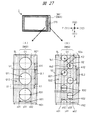
- FIG. 27 is a diagram showing a configuration example in plan view of a regulating portion on the first substrate side in FIG. 26 in the liquid crystal display device of the third embodiment.
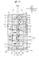
- FIG. 13 is a diagram showing a detailed configuration of the restricting portion and the like of the first configuration example in plan view in the liquid crystal display device of the third embodiment.
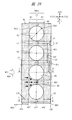
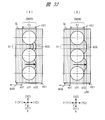
- FIG. 13 is a diagram illustrating a detailed configuration of a restricting portion and the like of a second configuration example in plan view in the liquid crystal display device of the third embodiment.
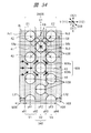
- FIG. 15 is a diagram showing a detailed configuration of a restricting portion and the like of a first modification in plan view in the liquid crystal display device of the third embodiment.
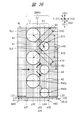
- FIG. 15 is a diagram showing a detailed configuration of a restricting portion and the like of a second modification in plan view in the liquid crystal display device of the third embodiment.
- FIG. 17 is a diagram illustrating a configuration of a restricting portion and the like in a third modification and a fourth modification in plan view in the liquid crystal display device of the third embodiment.
- FIG. 15 is a diagram illustrating a plan view of a configuration of a restricting portion and the like according to a fifth modification in the liquid crystal display device of the third embodiment.
- FIG. 16 is a diagram illustrating a configuration of a restricting portion and the like according to a sixth modification in plan view in the liquid crystal display device of the third embodiment.
- FIG. 16 is a diagram illustrating a configuration of a restricting portion and the like according to a seventh modification in plan view in the liquid crystal display device of the third embodiment.
- FIG. 21 is a diagram illustrating a configuration of a restricting portion and the like according to an eighth modification in plan view in the liquid crystal display device of the third embodiment.
- FIG. 21 is a diagram illustrating a plan view of a configuration of a restriction unit and the like according to a ninth modification example in the liquid crystal display device of the third embodiment.
- FIG. 21 is a diagram showing a plan view of a configuration of a restricting portion and the like according to a tenth modification in the liquid crystal display device of the third embodiment.
- FIG. 13 is a diagram illustrating a schematic configuration of a restricting portion and a sealing portion in plan view in a liquid crystal display device of a comparative example with respect to the third embodiment.
- the X direction is a direction corresponding to a short side or a horizontal direction in a screen
- the Y direction is a long side or a screen. This is a direction corresponding to the inner vertical direction or the like.
- the Z direction is a direction perpendicular to the plane in the X direction and the Y direction, and corresponds to the thickness direction. Further, for the sake of description, plan view mainly refers to a case where the XY plane is viewed in the Z direction.
- the liquid crystal display device according to the first embodiment of the present invention will be described with reference to FIGS.
- the liquid crystal display device of the first embodiment has an alignment film regulating portion outside the alignment film, and an inner end of the alignment film regulating portion which is in contact with the alignment film has an uneven shape in plan view (FIG. 4 and the like). .
- FIG. 1 shows a configuration of the liquid crystal display device 1 according to the first embodiment in an XY plane when the front surface on which the display surface is located is viewed in a plan view from the Z direction.
- the liquid crystal display device 1 corresponds to a liquid crystal display panel module applied to a portable information terminal device such as a smartphone.
- a direction X1 the left side in the figure is shown as a direction X1 and the right side is shown as a direction X2.
- the liquid crystal display device 1 has a cover member CVM when viewed from the front side.
- the cover member CVM is a member that protects the liquid crystal display device main body.
- a form without the cover member CVM is also possible.
- the front surface of the cover member CVM of the liquid crystal display device main body in FIG. 1 is roughly rectangular, and has a rectangular display area DA and a frame area FA outside (outer periphery) of the display area DA.
- the boundary between the display area DA and the frame area FA is indicated by a broken line in plan view.
- the display area DA corresponds to a display surface on which an image is displayed, and includes a plurality of pixels arranged in a matrix.
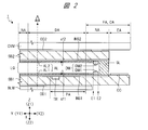
- FIG. 2 is a cross-sectional view (YZ plane) in the Y direction and the Z direction corresponding to the line AA in FIG. Show.
- the liquid crystal display device 1 includes a backlight module BLM, an optical element layer OD1, a first substrate SB1, a first alignment film AL1 as an alignment film AL, and a liquid crystal in order from a lower side (direction Z2) to an upper side (direction Z1) in the Z direction.
- It has a layer LQ, a second alignment film AL2 as an alignment film AL, a second substrate SB2, an optical element layer OD2, and a cover member CVM. Note that the thickness of the liquid crystal layer LQ is actually thinner than the first substrate SB1 and the second substrate SB2.
- a rigid housing or the like may be provided outside the liquid crystal display device main body.
- the first substrate SB1 is an array substrate on which the transistors TR, various electrodes (conductor patterns), and the like are arranged.
- the second substrate SB2 is a counter substrate facing the first substrate SB1 and on which color filters and the like are arranged.
- the first surface sf1 of the first substrate SB1 and the second surface sf2 of the second substrate SB2 face each other and are disposed so as to interpose a liquid crystal layer LQ or the like therebetween.
- the sealing portion SL adheres between the first surface sf1 of the first substrate SB1 and the second surface sf2 of the second substrate SB2, and seals the liquid crystal layer LQ inside.
- the liquid crystal layer LQ forms a liquid crystal cell associated with a pixel.
- the display area DA is constituted by the first substrate SB1, the second substrate SB2, the liquid crystal layer LQ, pixel electrodes described later, and the like.
- the display area DA overlaps the liquid crystal layer LQ in plan view.
- the display area DA has a pixel area PA for each pixel.
- FIG. 2 illustrates an example of the pixel region PA at the outermost end in the Y direction (direction Y2) and the transistor TR in the pixel region PA.
- the display area DA is an area where the uniformity of the optical characteristics of each pixel is ensured.
- the first surface sf1 of the first substrate SB1 is, for example, the surface of the insulating film INS1 on the upper side of the transistor TR and the like.
- an alignment film (first alignment film) AL1 On the first surface sf1 (direction Z1) of the insulating film INS1, an alignment film (first alignment film) AL1, a regulating portion DM1, a sealing portion SL, and the like are formed.
- the second surface sf2 of the second substrate SB2 is, for example, the surface of the insulating film INS2.
- an alignment film (second alignment film) AL2, a regulating portion DM2, a sealing portion SL, and the like On the second surface sf2 (direction Z2), an alignment film (second alignment film) AL2, a regulating portion DM2, a sealing portion SL, and the like are formed.
- the term “formed on” in the present specification includes a form formed via some kind of member.
- the sealing portion SL is provided in the frame region FA outside the liquid crystal layer LQ and the display region DA.
- the sealing portion SL is made of an adhesive or the like, and bonds the insulating film INS1 of the first substrate SB1 and the insulating film INS2 of the second substrate SB2, and seals liquid crystal molecules of the liquid crystal layer LQ inside.
- the frame area FA has a regulating portion DM.
- the regulating portion DM (DM1, DM2) is provided at a position inside the sealing portion SL in the Y direction.
- a regulating portion DM1 is provided adjacent to an end of the first alignment film AL1.
- a regulating part DM2 adjacent to an end of the second alignment film AL2.
- the restricting portion DM1 restricts the spread of the first alignment film AL1.
- the restricting portion DM2 restricts the spread of the second alignment film AL2.
- the first substrate SB1 is longer than the second substrate SB2 and has an extended area EA.
- the extension region EA is shown as a region from the end of the second substrate SB2 to the end of the first substrate SB1.
- a non-display area NA is provided outside the display area DA and inside from the end of the second substrate SB2.
- the non-display area NA includes the end areas of the alignment films AL1 and AL2, the restriction sections DM (DM1 and DM2), the sealing section SL, and the like. These elements are included in the non-display area NA in order to ensure uniform display of each pixel (pixel area PA) in the display area DA.
- the circuit section CC is provided at a position outside the sealing section SL and the like so as to be exposed.
- the circuit portion CC includes a terminal portion connected to an electrode or a wiring in the first substrate SB1, a wiring further connected to the terminal portion, an integrated circuit (for example, an IC chip) connected to the wiring. .
- a flexible printed circuit board or the like may be connected to the circuit section CC.
- the circuit section CC constitutes a driving circuit of the liquid crystal display device 1 and the like. In the extension area EA, the circuit section CC may be mounted as described above.
- the first substrate SB1 has the optical element layer OD1 disposed on the lower surface (direction Z2) in the Z direction, and the backlight module BLM disposed on the lower surface of the optical element layer OD1.
- the backlight module BLM emits light and supplies light (indicated schematically by an alternate long and short dash line arrow) in the upper direction Z1 in the Z direction.
- the light from the backlight module BLM passes through the first substrate SB1, the liquid crystal layer LQ, the second substrate SB2, and the like in the Z direction, is optically modulated by the liquid crystal cell, and becomes visible light of pixels as eyes of the user. Incident.
- the optical element layer OD2 is arranged on the upper surface in the Z direction (direction Z1), and the cover member CVM is arranged on the upper surface of the optical element layer OD2.
- Each of the optical element layer OD1 and the optical element layer OD2 includes a polarizing plate, and may include a retardation plate or the like as necessary.
- the regulating portions DM1 and DM2 are provided at the same position in the Y direction on both the first substrate SB1 and the second substrate SB2.
- the restricting portion DM1 has a shape like a frame or a wall which rises upward (direction Z1) in the Z direction on the first surface sf1 in order to restrict the spread of the end portion of the alignment film AL1.
- the restricting portion DM1 has a side surface in contact with an end of the alignment film AL1 in its shape. It is preferable that the height of the regulating portion DM1 is higher than the height of the end of the alignment film AL1.
- the restricting portion DM2 has a shape that protrudes downward in the Z direction (direction Z2) on the second surface sf2 in order to restrict the spread of the end portion of the alignment film AL2.
- the shape of the restriction portions DM1 and DM2 is not limited to a raised shape.
- the following is a configuration example of known pixels and circuits of the liquid crystal display device 1.
- the pixel is composed of, for example, sub-pixels of three colors of red (R), green (G), and blue (B).
- the sub-pixel is provided with a transistor TR (FIG. 2) as a switching element, a liquid crystal cell of a liquid crystal layer LQ, a pixel electrode, a common electrode, a color filter, and the like in association with each other.
- One pixel is configured at a portion where a scanning line and a video signal line intersect.
- a color filter for each color is arranged in the opening of the sub-pixel, and a transistor TR, a light shielding film, and the like are arranged in the non-opening.
- the transistor TR is formed of, for example, a thin film transistor, and has a gate terminal connected to a scanning line, a source terminal connected to a video signal line, and a drain terminal connected to a pixel electrode.
- the scanning lines are connected to a scanning line driving circuit, and a plurality of scanning lines extend in parallel in the X direction.
- the scanning line driving circuit supplies a scanning signal for selecting a pixel to the scanning line.
- the video signal lines are connected to a video signal line drive circuit, and a plurality of video signal lines extend in parallel in the Y direction.
- the video signal line driving circuit supplies a video signal for controlling the gradation of the sub-pixel to the video signal line.
- a liquid crystal cell and a storage capacitor are provided between the pixel electrode and the common electrode, and are electrically connected via the liquid crystal cell.
- the common electrode is connected to a common electrode drive circuit.
- the common electrode drive circuit supplies a common voltage to the common electrode.
- Each drive circuit is connected to a control circuit.
- the control circuit performs drive control and the like of each circuit based on the image signal.
- the drive circuit and the control circuit are implemented by, for example, the circuit unit CC in FIG.
- FIG. 3 shows a schematic configuration of regions such as the frame region FA and the regulating portion DM1 on the front surface (XY plane) of the liquid crystal display device 1 according to the first embodiment. Correspondingly, a schematic configuration of a cross section (YZ plane) is shown on the lower side. FIG. 3 also shows a schematic configuration relating to a method of forming the regulating portion DM1 using an inkjet method described later.
- the frame area FA on the outer circumference of the display area DA has a first outer circumference area L1 (corresponding to the lower side) on the lower side (direction Y2) in the Y direction, and a second outer circumference area on the upper side (direction Y1).
- L2 (corresponding to the upper side), a third outer peripheral area L3 (corresponding to the left side) on the left side (direction X1) in the X direction, and a fourth outer peripheral area L4 on the right side (direction X2). (Corresponding to the right side).
- the first substrate SB1 has a first extended region EA1 on the lower side in the Y direction as an extended region EA.
- the first outer peripheral area L1 (first extension area EA1) has a first circuit area CA1.
- the first outer peripheral area L1 has a non-display area NA1.
- the first circuit area CA1 includes a first drive circuit section CD1.
- the first drive circuit portion CD1 is a portion where the drive circuit and the like of the liquid crystal display device 1 are mounted, corresponds to the circuit portion CC in FIG. 2, and includes the above-described terminal portion and the like.
- the other peripheral area does not have an exposed circuit section (terminal section or the like) such as the first drive circuit section CD1.
- a frame-shaped mounting area 301 on the outer periphery of the display area DA indicates an area where the restricting portions DM (DM1, DM2) and the sealing portion SL are mounted.
- the range of the mounting area 301 includes the restricting portion DM and the sealing portion SL.
- the mounting area 301 becomes a non-display area NA.
- the regulation part DM1 will be mainly described, the regulation part DM1 and the regulation part DM2 have the same configuration.
- Regulator DM1 includes a lower-side restrictor DM11, an upper-side restrictor DM12, a left-side restrictor DM13, and a right-side restrictor DM14.
- the lower side portion in the Y direction includes a lower side regulating portion DM11
- the upper side portion in the upper side includes an upper side regulating portion DM12.
- the left side portion on the left side (direction X1) in the X direction includes the left side regulating portion DM13
- the right side portion on the right side (direction X2) includes the right side regulating portion DM14.
- the lower side regulating section DM11 and the upper side regulating section DM12 are constituted by a first regulating section DMA
- the left side regulating section DM13 and the right side regulating section DM14 are constituted by a second regulating section DMB.
- the first restricting unit DMA is shown as an image of a continuous area of circles.
- the second regulating portion DMB is shown by an image of a linear region.
- the first restricting portion DMA has a concavo-convex shape (FIG. 4) described later.
- the second regulating portion DMB has a linear shape (FIG. 20) described later.
- the entire width H1 of the first regulating portion DMA particularly the width in the Y direction, is indicated by a width H11.
- the entire width H1 of the second regulating portion DMB, particularly the width in the X direction, is indicated by a width H12.
- the width H11 and the width H12 are the same, but in a modified example, the width H11 and the width H12 may be different.
- first regulating portion DMA and second regulating portion DMB are provided in this manner for the following reasons.
- first regulating portion DMA and second regulating portion DMB are provided in this manner for the following reasons.
- the width including the first extension area EA1 is larger. Tends to be large.
- the third outer peripheral area L3 and the fourth outer peripheral area L4 corresponding to the left and right sides have a small or no mounting area for the drive circuit and the like.
- a scanning line driving circuit connected to the scanning lines is mounted inside the first substrate SB1 because of the narrow frame configuration. Therefore, in the third outer peripheral region L3 and the fourth outer peripheral region L4, the width in the X direction is smaller than the width in the Y direction such as the first outer peripheral region L1. For this reason, in the left and right sides, the second regulating portion DMB in which the regulating force of the alignment film AL is strong is applied, which is the same as in the related art.
- the regulating force of the second regulating portion DMB it is possible to further prevent problems such as the alignment film varnish getting over the regulating portion.
- the importance of the width reduction is higher than in the third outer peripheral area L3 and the like, so the first restricting unit DMA is applied.
- the length of the first outer peripheral region L1 (first circuit region CA1) in the Y direction is 1000 ⁇ m or less as a narrow frame configuration realized by including the operation of the regulating portion DM.
- the present invention is not limited to the configuration shown in FIG.
- the first regulating unit DMA may be provided in the liquid crystal display device 1 according to the modified example of the first embodiment.
- the first restricting portion DMA may be provided on all four sides (outer peripheral region) of the frame area FA.
- the first restricting portion DMA may be provided only in the upper side portion and the lower side portion of the frame area FA.
- the first restricting portion DMA may be provided only in the lower side portion (first outer peripheral region L1) of the frame region FA.
- a configuration may be such that the regulating portion DM is not provided on the left and right sides of the frame area FA.
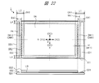
- FIG. 22 shows the configuration of the front surface (XY plane) of the liquid crystal display device 1 according to a modification of the first embodiment.
- the extended region EA of the first substrate SB1 in the overlap between the first substrate SB1 and the second substrate SB2, the extended region EA of the first substrate SB1 has the first extended region EA1 on the lower side in the Y direction, Side has a second extension area EA2.
- the circuit area CA has a first circuit area CA1 in a first outer peripheral area L1 (first extended area EA1) and a second circuit area CA2 in a second outer peripheral area L2 (second extended area EA2).
- the first restricting portion DMA (lower-side restricting portion DM11 and upper-side restricting portion DM12) is provided in the lower side portion and the upper side portion of the frame area FA in the Y direction. Further, in this configuration, the regulating portions DM are not provided on the left and right sides of the frame area FA.
- FIG. 4 is a plan view (XY) of the liquid crystal display device 1 according to the first embodiment of the restricting portion DM1 on the first substrate SB1 side (particularly, corresponding to the lower restricting portion DM11 and the first restricting portion DMA in FIG. 3). Plane).
- the regulating portion DM2 on the second substrate SB2 side has the same configuration.
- FIG. 4 shows a model shape relating to the shape of the regulating portion DM1, and the actual shape may be different from the shape of FIG. 4 depending on the forming method and the like.
- the shape of the restricting portion DM11 is roughly a concavo-convex shape along the X direction, and is configured by a series of a plurality of circles extending in the X direction as shown in the figure.
- the plurality of circles are continuous with each other, and there is no gap between the circles.
- the shape of the regulating portion DM11 is symmetrical with respect to the center line C1 indicating the arrangement center position, but may be asymmetrical.
- the restriction part DM11 has an inner end E1 and an outer end E2.
- the inner end E1 is an end facing the display area DA and in contact with the alignment film AL1.
- the outer end E2 is an end opposite to the inner end E1.
- the position of the innermost end E1 in the Y direction (direction Y1) that is the innermost is indicated by a line a1
- the position of the outer end E2 that is the outermost in the Y direction (the direction Y2) is a line a2. Show.
- the inner end portion E1 has an uneven shape for restricting the spread of the alignment film AL1 and suppressing unevenness of the rebound.
- the inner end portion E1 corresponds to a portion having the uneven shape.
- the line at the end near the center line C1 side in the uneven shape of the inner end E1 is indicated by a line b1.
- a line at the end near the center line C1 side in the uneven shape of the outer end portion E2 is indicated by a line b2.
- FIG. 4 shows a center line c1 in the Y direction in the uneven shape of the inner end E1, and a center line c2 in the Y direction in the uneven shape of the inner end E2.
- the uneven shape of the inner end portion E1 has a concave portion 41 and a convex portion 42. It has a plurality of concave portions 41 and a plurality of convex portions 42 in the X direction, and the concave portions 41 and the convex portions 42 are arranged alternately.
- the plurality of concave portions 41 are arranged at a predetermined interval pt1.
- the plurality of convex portions 42 are arranged at a predetermined interval pt1.
- the concave portion 41 is a portion that enters the direction Y2 between the line a1 and the line b1, and is located between the adjacent convex portions 42 in the X direction.
- the convex portion 42 is a portion that extends in the direction Y1 between the line a1 and the line b1, and is located between the concave portions 41 on both sides in the X direction.
- the convex portion 42 is made of the material of the regulating portion, but the concave portion 41 is a portion other than the material of the regulating portion.
- the concave-convex shape of the inner end portion E1 is a shape in which a plurality of arcs are continuous on the side surface.
- the width H1 indicates the width (entire width) in the Y direction of the entire regulation portion DM1.
- the width H2 indicates a width in the Y direction at a half of the regulating portion DM1 from the center line C1 toward the inner end E1.
- the width W1 indicates, as the first width, the width in the Y direction of the inner end portion E1 (concavo-convex shape), the concave portion 41, and the convex portion 42.
- the width W2 indicates, as the second width, the maximum width in the Y direction of the regulating portion DM1 at each position (for example, positions p1 to p4) in the direction along the uneven shape of the inner end portion E1.
- the width W2 is a width at the position (the innermost position) p4 of the tip of the projection 42, in particular. In this example, the width W2 is equal to the width H1, but it is not limited to this.
- the shape of the regulating portion DM1 satisfies the condition that the width W1 is equal to or less than the width W2 (W1 ⁇ W2).
- the interval pt1 is within the range of the predetermined interval.
- the width W1 is particularly 100 ⁇ m or less (W1 ⁇ 100 ⁇ m).
- the shape of the regulating portion DM1 may be a shape having only half of the center line C1 on the inner end portion E1 side. On the outer end E2 side, the regulating portion DM1 does not have an uneven shape but has an arbitrary shape such as a linear shape.
- the width W2 the width H2.
- the shape of the projection 42 is not limited to a circle having a constant radius, but may be an ellipse, a free-form surface, or the like.
- a direction 401 (corresponding to the direction Y2) indicates a main spreading direction of the alignment film varnish when the alignment film AL1 is formed on the first surface sf1.
- the spreading of the alignment film varnish is stopped by hitting the inner end portion E1, and rebound occurs.
- the direction 402 is a direction opposite to the direction 401 (corresponding to the direction Y1), and indicates a main rebound direction of the alignment film varnish.
- the alignment film varnish hits a curved surface (a slope with respect to the direction 401) of the convex portion 42
- the alignment film varnish reflects along the curved surface direction and enters the concave portion 41. Due to such an uneven shape of the inner end portion E1, the rebound of the alignment film varnish in the direction 402 (direction Y1) is reduced, and the width of the uneven region due to the rebound is reduced. Details are shown in FIGS. 13 and 14 described later.
- the concavo-convex shape of the regulating portion DM1 in FIG. 4 can be formed by various methods.
- the concave-convex shape of the regulating portion DM1 in FIG. 4 is formed by using an inkjet type liquid crystal display device manufacturing method (including a regulating portion forming method). That is, at the time of manufacturing, in the step of forming the regulating portion DM1 on the first substrate SB1, droplets of the regulating portion material constituting the regulating portion DM1 are ejected from the head of the inkjet device. This droplet corresponds to each circle in FIG.
- a regulating portion DM1 as shown in FIG. 4 can be formed.
- the droplets of the regulating portion material discharged on the first surface sf1 are solidified by, for example, drying by temperature control.
- the material of the regulating portion DM1 (the regulating portion material) is selected based on the relationship with the alignment film AL1 and the sealing portion SL.
- the regulating part material has liquid repellency to the material of the alignment film AL1 (alignment film varnish).
- the alignment film varnish is, for example, a solution in which a solute alignment material is mixed in a solvent.
- the regulating portion material is, for example, an organic material. This liquid repellency means that the regulation part material in a solidified state has poor compatibility with the alignment film varnish (in other words, high incompatibility). If the compatibility is poor, the substance of the regulating portion material and the alignment film varnish are separated, and a lyophobic phenomenon occurs. Thereby, the regulation part DM1 can more effectively reduce the spread and the rebound of the alignment film AL1.
- the regulating unit DM2 The same applies to the regulating unit DM2.
- a cyclic amide-based solvent such as N-methyl-2-pyrrolidone or a cyclic ester-based solvent such as ⁇ -butyrolactone having high solubility of the compound is used.
- a polyimide material having high compatibility with the cyclic amide solvent and a cyclic ester solvent are different from each other.
- a polyimide obtained by imidizing a polyamic acid or a polyamic acid ester represented by the following chemical formula (1) or (2) is used as an alignment film material.
- polyamic acid and polyamic acid ester have different organic solvents having high compatibility with each other.
- Ar is an organic group
- R a and R b are each independently hydrogen or an alkyl group having 1 to 6 carbon atoms.
- ⁇ -butyrolactone is used as a main solvent of the alignment film varnish. Therefore, if the regulating portion is formed of polyamic acid, the compatibility between ⁇ -butyrolactone of the alignment film varnish and the regulating portion is poor. Therefore, it is difficult for the alignment film varnish to get over the regulating portion.
- the amount of polyamic acid is large in the alignment film material (for example, 80% by mass or more based on the total solid content)
- N-methyl-2-pyrrolidone is used as the main solvent of the alignment film varnish.
- the regulating portion is formed of a polyamic acid ester
- the compatibility between N-methyl-2-pyrrolidone of the alignment film varnish and the regulating portion is poor. Therefore, it is difficult for the alignment film varnish to get over the regulating portion.
- each polyamic acid or polyamic acid ester is finally changed to polyimide in the production process.
- one of the alignment film and the regulating portion is a polyimide derived from a polyamic acid, and the other is a polyimide derived from a polyamic acid ester.
- the above description is only an example of the liquid-repellent phenomenon of the alignment film varnish. Therefore, if it is difficult for the alignment film varnish to get over the regulation portion, the orientation film and the regulation portion may be formed of another material.
- FIG. 5 is a schematic configuration of the first embodiment in a cross section (YZ plane) of the restricting portion DM1 (particularly, the lower-side restricting portion DM11) in the Y direction and the Z direction corresponding to the line CC in FIG. Is shown.
- FIG. 5 shows the ends of the regulating portion DM1 and the alignment film AL1 on the first surface sf1 which is the upper surface of the insulating film INS1 of the first substrate SB1.
- the first surface sf1 is the ground below the alignment film AL1 and the regulating portion DM1, and is at the same height position.
- the cross-sectional shape of the regulating portion DM1 in FIG. 5 is roughly concave, is lower at the center position y0 in the Y direction, and is an outer position corresponding to the inner end portion E1 and the outer end portion E2. It is higher at positions near y1 and y2.
- the thickness of the alignment film AL1 in the Z direction is indicated by a thickness T2
- the thickness of the regulating portion DM1 is indicated by a thickness T1.
- the thickness T1 of the regulating portion DM1 is larger than the thickness T2 of the alignment film AL1 (T2 ⁇ T1).
- the regulating portion DM1 is higher than the alignment film AL1.
- the thickness T1 of the regulating portion DM1 is 1000 nm or less (T1 ⁇ 1000 nm).
- thickness T1 is at least 150 nm.
- the restricting portion DM1 in FIG. 5 is formed by using an ink jet method. That is, the droplets of the regulating portion material are ejected from the nozzles of the head of the inkjet device in the direction Z2 to the first surface sf1, whereby the regulating portion material is applied onto the first substrate SB1. The droplets are solidified by drying or the like, thereby forming the regulating portion DM1. At this time, the concave shape of the regulating portion DM1 is formed by the same principle as the known coffee stain phenomenon (the principle that the concentration of the solute in the outer peripheral portion is higher than that in the central portion). The same applies to the restriction unit DM2.
- FIG. 5 particularly shows a cross section at a position of a certain convex portion 42, and the height of the end portion of the alignment film AL1 is equal to or less than the height (thickness T1) of the inner end portion E1 of the regulating portion DM1.
- the height of the end of the alignment film AL1 may be larger than the height (thickness T1) of the inner end E1 of the regulating part DM1.
- FIG. 6 shows a schematic configuration of a cross-sectional shape of the regulating portion DM1 and the alignment film AL1 in a modification example of FIG.
- the end of the alignment film AL1 has a shape that rises beyond the height (thickness T1) of the inner end E1 of the regulating portion DM1.
- FIG. 6 shows a cross section at a position of a certain concave portion 41 (for example, line DD in FIG. 4). Since the raised end is within the non-display area NA, it does not affect the display area DA.
- the end of the alignment film AL1 may enter the concave shape of the regulating portion DM1.
- FIG. 23 shows a schematic configuration of a cross-sectional shape of the regulating portion DM1 and the alignment film AL1 in a modified example.
- the cross-sectional shape of the restricting portion DM1 is roughly convex, and is higher at the center position y0 in the Y direction and lower at outer positions y1 and y2. Even with such a shape of the regulating portion DM1, the effect of reducing the unevenness at the edge of the alignment film can be obtained similarly.
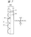
- FIG. 7 shows a schematic configuration of a liquid crystal display device 1 according to a modified example of the first embodiment in plan view of the regulating portion DM1.
- the regulating portion DM1 in FIG. 7 corresponds to a half configuration on the inner end E1 side of the regulating portion DM1 in FIG.
- the outer end E2 is linear.
- the uneven shape of the inner end portion E1 is a shape formed by repeating a plurality of semicircles.
- FIG. 8 shows a schematic configuration of another example of the modification in a plan view of the regulating portion DM1.
- the regulating part DM1 in FIG. 8 has a wave shape at the inner end E1.
- the convex portion 42 has a curved surface projecting in the direction Y1 with respect to the center line c1, and the concave portion 41 has a curved surface entering the direction Y2 in the opposite direction.
- This wave shape may be a shape such as a sine wave.
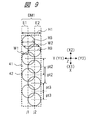
- FIG. 9 shows a schematic configuration of another example of the restriction portion DM1 in plan view.
- a series of a plurality of circles are arranged in the X direction along center lines j1 and j2 at two positions in the Y direction.
- the circles of the plurality of circles are intermittently arranged at predetermined intervals pt2 while providing a gap between the circles.
- the circles are arranged at a predetermined interval pt3.
- the regulating portion DM1 has a concave portion 41 and a convex portion 42 at the inner end E1 as a whole.
- the concave portion 41 is formed by two circles adjacent in the X direction on one center line j1 closer to the inside, and a circle on the other center line j2 therebetween.
- the convex portion 42 is formed by a part of one circle on the center line j1 between two circles on the center line j2.
- the width H3 indicates a width (a maximum width of one circle) in a row of circles on one center line j1.
- the width of the row of circles on the other center line j2 is the same as the width H3.
- the width W1 and the width W2 can be obtained as in the case of FIG.
- the width W1 is as shown and corresponds to the distance between the inner end of the circle on one line and the inner end of the circle on the other line.
- the width W2 is as shown, and is the maximum width in a portion where two circles in two rows are continuous.
- the shape of the regulating portion DM1 of this modification can also be formed by an ink jet method in particular. That is, the head position, the nozzle position, and the like may be controlled such that the droplets of the regulating portion material are ejected from the head of the inkjet apparatus at the positions of the two center lines j1 and j2, respectively. Further, it is only necessary to control the interval and the size (pressure, etc.) of the droplets when the droplets are ejected from the nozzles of the head during scanning by the inkjet device.
- the detailed shape of the concavo-convex shape of the regulating portion DM can be controlled by the control by the inkjet device.
- the invention is not limited to the formation of droplet groups in two rows as described above, and may be formed in three or more rows.
- a conventional inkjet apparatus ejects a plurality of liquid droplets along the X direction, if a positional shift in the Y direction occurs, the characteristic of the positional shift is used to control such a regulating unit.
- An uneven shape of DM can be formed.
- FIG. 10 shows a schematic configuration of another example of the restriction portion DM1 in a plan view.
- the shape of the regulating portion DM1 in FIG. 10 is a shape that meanders or vibrates in the Y direction (directions Y1 and Y2) along the center line C1.
- both the inner end E1 and the outer end E2 have irregularities.
- the inner end portion E1 has a concave portion 41 and a convex portion 42, and has a slope by a wave curve.
- the width W1 and the width W2 can be similarly set.
- the shape of the restriction portion DM1 can be formed, for example, by controlling the meandering and vibration of the position in the Y direction when applying the material of the restriction portion along the X direction by a manufacturing apparatus during manufacturing.
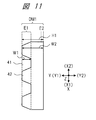
- FIG. 11 shows a schematic configuration of another example of a modification of the restricting portion DM1 in plan view.
- the shape of the restricting portion DM1 has a trapezoidal concave portion 41 and a convex portion 42 at the inner end E1.
- the trapezoid of the concave portion 41 and the convex portion 42 has a short side extending in the X direction and an oblique side that is oblique to the Y direction from the short side.
- the width W1 and the width W2 can be similarly set.
- the outer end E2 may have the same shape as the inner end E1.
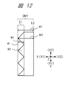
- FIG. 12 shows a schematic configuration of another modification of the restricting portion DM1 in plan view.
- the shape of the restricting portion DM1 has a triangular concave portion 41 and a convex portion 42 at the inner end E1.
- the triangle of the concave portion 41 and the convex portion 42 has a hypotenuse that is oblique to the Y direction.
- the width W1 and the width W2 can be similarly set.
- the outer end E2 may have the same shape as the inner end E1.
- FIG. 20 illustrates the first restricting unit DMA of the first embodiment with respect to the restricting unit 201 in the liquid crystal display device of the first comparative example with respect to the first embodiment, and the second restricting unit DMB (FIG. 3) of the first embodiment.
- the schematic configuration in a plan view is shown by comparison with FIG.
- the concave and convex shape of the inner end portion E1 of the first restricting portion DMA in the first embodiment is provided with a width W1 (particularly, a width W11) of a predetermined size or more.
- the first width (width W11) of the inner end portion E1 of the first regulating portion DMA is larger than the first width (width W12) of the inner end portion E1 of the regulating portion 201 (second regulating portion DMB) (W11> W12).
- FIG. 21 shows a schematic plan view of the configuration of the restriction unit 202 in the liquid crystal display device of the second comparative example with respect to the first embodiment in comparison with the first restriction unit DMA of the first embodiment.
- the shape of the restricting portion 202 is a zigzag shape extending at a predetermined width along a center line C1 extending in the X direction.
- the width H4 indicates a width in a direction perpendicular to the zigzag direction.
- the zigzag side surfaces (inner end and outer end) have a triangular wave shape.
- a first width (width W1, particularly width W13) and a second width (width W2, particularly width W23) of the concave portion 241 and the convex portion 242 are considered.
- the width W1 (W13) is larger than the width W2 (W23) (W1> W2).
- the width W1 (W11) is equal to or less than the width W2 (W1 ⁇ W2).
- the interval between the protrusions 242 in the zigzag X direction of the regulating portion 202 in the X direction is indicated by an interval pt4.
- the interval pt4 of the formation of the irregularities in the regulating portion 202 is larger than the interval pt1 of the irregularities of the regulating portion DM1 in the first embodiment (pt4> pt1).
- the concavo-convex shape of the regulating portion DM1 in the first embodiment is formed on a smaller scale than the zigzag shape of the regulating portion 202. In the case of such a restricting portion 202, on the inner end side, each slope of the zigzag shape is linear.
- FIG. 13 shows a schematic configuration in plan view, comparing the restricting unit 201 of the first comparative example as shown in FIG. 20 with the configuration example of the restricting unit DM1 (first restricting unit DMA) in the first embodiment.
- Show. 13A shows an alignment film varnish region 131 corresponding to an end of the first alignment film AL1 and a linear regulating portion 201 on the flat first surface sf1.
- the restricting portion 201 extends in the X direction.
- the coating liquid corresponding to the alignment film varnish basically spreads in the direction 401 corresponding to the direction Y2.
- the alignment film varnish is rebounded in the direction 402. As a result, an uneven region 132 of the alignment film varnish is generated. In the uneven region 132, the degree of rebound of the material is different at each position in the X direction, and the thickness and shape are uneven.
- the width of the uneven region 132 in the Y direction is indicated by a width M1.
- the right side shows a cross section of the restricting portion 201 and the like.
- the total width (H1 + M1) of the width H1 of the regulating portion 201 and the width M1 of the uneven area 132 is shown.
- the uneven area 132 is included in the non-display area NA because uniformity of optical characteristics of pixels cannot be ensured. Accordingly, the display area DA becomes smaller and the frame area FA becomes larger.
- FIG. 13B shows, on a flat first surface sf1, a region 133 of an alignment film varnish corresponding to an end of the first alignment film AL1 and a regulating portion DM1 having an uneven shape.
- the shape of the restricting portion DM1 is an example of a shape in a case where there is a positional shift within a predetermined range in the Y direction at the time of forming by the ink jet method based on the model shape of FIG.
- the coating liquid corresponding to the alignment film varnish basically spreads in the direction 401 corresponding to the direction Y2.
- the alignment film varnish hits the inner end E1 of the regulating portion DM1 and rebounds in the opposite direction 402. As a result, an uneven region 134 of the alignment film varnish is generated.
- the width in the Y direction of the uneven region 134 is indicated by a width M2.
- the width M2 is smaller than the width M1 (M2 ⁇ M1).
- the unevenness of the inner end portion E1 mitigates the difference in rebound of the material at each position in the X direction so as to be small.
- the alignment film varnish hits the curved surface (slope) of the concave portion 41 and the convex portion 42 and is reflected in a direction corresponding to the curved surface (slope).
- the wave energy of the coating liquid is dispersed in oblique directions different from the directions 401 and 402 due to the uneven shape of the inner end E1.
- the width M2 of the uneven area 134 becomes smaller than the width M1.
- the width M2 is a length from the position of the innermost portion in the Y direction in the uneven shape of the inner end portion E1 to the innermost position of the uneven region 133.
- the right side shows a cross section of the restriction portion DM1 and the like.
- the total width (H1 + M2) of the width H1 of the regulating portion DM1 and the width M2 of the uneven area 134 is shown.
- This overall width (H1 + M2) is smaller than the overall width (H1 + M1) of the comparative example.
- the width M2 of the uneven region 134 can be further reduced.
- the overall width (H1 + M2) including the width M2 of the uneven region 134 can be suppressed. Therefore, the non-display area NA (frame area FA) can be made smaller and the display area DA can be made larger.
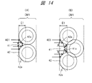
- FIG. 14 schematically shows the rebound of the alignment film varnish with respect to the uneven shape of the inner end E1 of the regulating portion DM1.
- A shows the case of the first example of the shape of the restricting portion DM1, which is based on the model shape of FIG.
- B shows the case of the second example of the shape of the restricting portion DM1, which is based on the shape of the modification of FIG.
- Each ring-shaped circle corresponds to one droplet of the ink jet system.
- the molecules of the alignment film varnish hit the curved surface (slope) 42a of the convex portion 42 of the inner end E1 in the direction 401 (direction Y2) indicated by each arrow, and correspond to the direction of the inclination of the curved surface 42a.
- the molecules of the alignment film varnish have a curved surface (slope) 42a of the convex portion 42 and a curved surface (slope) 41a of the concave portion 41 in the direction 401 (direction Y2) indicated by each arrow. Is reflected in a direction corresponding to the direction of inclination of the curved surface 42a or the curved surface 41a. As described above, since the directions of the rebound of the molecules of the alignment film varnish are dispersed, the width M2 of the uneven region 134 is reduced as a whole.
- a regulating portion DM1 having an uneven shape as shown in FIG. 4 is formed on the first surface sf1 of the first substrate SB1 by using an inkjet method.
- the outline of the method of forming the regulating portion DM1 and the alignment film AL1 is as follows.
- the ink jet device applies the regulating portion material to the first surface sf1 of the insulating film INS1 of the first substrate SB1 by discharging droplets of the regulating portion material (varnish).
- the manufacturing apparatus solidifies the regulating portion material on the first substrate SB1 by drying or the like. Thereby, the regulating portion DM1 is formed.
- the manufacturing apparatus applies an alignment film varnish of the first alignment film AL1 to a region inside the regulating portion DM1.
- an ink jet device is used.
- the ink jet device applies the alignment film varnish to the area by discharging droplets of the alignment film varnish.
- the unnecessary spread of the alignment film varnish is regulated by the regulating portion DM1, and unevenness at the end is suppressed.
- the manufacturing apparatus solidifies the alignment film varnish of the first alignment film AL1 on the first substrate SBI by drying or the like. (6) The manufacturing apparatus reacts the regulating portion material on the first substrate SB1 and the alignment film varnish of the first alignment film AL1 on the first substrate SBI by firing or the like. (7) The manufacturing apparatus performs an alignment process on the alignment film AL1 using, for example, a photo alignment method. Thus, an alignment film AL1 is formed.
- the restriction portion DM2 and the alignment film AL2 on the second substrate SB2 side can be formed in the same manner as described above.
- the details of the method of forming the regulating portion DM1 are as follows.
- the uneven shape of the regulating portion DM1 is easily and efficiently formed by utilizing the characteristics of the ink jet method.
- two types of regulating portions are formed by utilizing a difference in accuracy between a main scanning direction in which a rail for an inkjet head extends and a sub-scanning direction crossing the main scanning direction.
- An overview of the main scanning direction and the sub-scanning direction is disclosed, for example, in FIG. 3 of US Publication No. 2014/0062076.
- a direction DIR1 indicated by a solid arrow indicates the main scanning direction of the inkjet head
- a direction DIR2 indicated by a broken arrow indicates the sub-scanning direction of the head.
- the direction DIR1 corresponds to the Y direction
- the direction DIR2 corresponds to the X direction.
- the ink jet device performs line-sequential scanning when applying a material.
- the ink jet device scans the head linearly in a direction DIR1 along a rail of the ink jet device. Then, the inkjet apparatus performs sub-scanning so as to move the head in the direction DIR2 each time scanning of one line is completed.
- the ink jet device ejects liquid droplets of a material from nozzles of the head during main scanning of the head.
- the ink jet device controls whether or not the control section material is ejected in the area where the control section DM1 is formed and the area where the control section DM1 is not formed during scanning.
- the head In the main scanning in the direction DIR1, the head can be continuously moved along the carriage rail, but in the sub-scanning in the direction DIR2, the head or the medium to be ejected needs to be mechanically moved.
- the accuracy of movement is lower than that of main scanning. That is, in the sub-scanning direction DIR2, the accuracy of the position and interval of material formation (ejection) is inferior to the main scanning direction DIR1. Therefore, in this forming method, the region and direction of the uneven shape of the first regulating portion DMA correspond to the direction DIR2 of the sub-scanning of the head.
- the head In the sub-scanning direction DIR2, the head is moved by mechanical driving.
- the positions and intervals of the ejection of the droplets in the X direction in the region where the first regulating portion DMA is formed are determined. This interval is wider than the interval of the ejection of the droplets in the Y direction in the area of the second regulating portion DMB. Thereby, an uneven shape in the first regulating portion DMA can be formed.
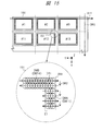
- FIG. 15 shows an explanatory view of an example of the manufacturing method.
- FIG. 15 shows a schematic plan view of a case where a plurality of liquid crystal display main bodies (or the first substrate SB1 or the like) are collectively formed on a mother substrate 150, and each liquid crystal display main body is formed by cutting. Is shown. Numbers # 1 to # 3 and the like denote individual liquid crystal display device main bodies.
- Each liquid crystal display device main body includes a regulation part DM1 on the first substrate SB1.
- the regulating portion DM1 When the regulating portion DM1 is formed, the main scanning of the ink jet method is performed in the direction DIR1 (corresponding to the Y direction) as described above, and the sub-scanning is performed in the direction DIR2 (corresponding to the X direction). As a result, the first regulating portions DMA extending in the X direction and the second regulating portions DMB extending in the Y direction are collectively formed for the plurality of liquid crystal display device bodies. After the formation, the individual liquid crystal display device main bodies are taken out by cutting from the mother substrate 150. In each liquid crystal display device main body, four sides on the outer periphery are formed.
- each liquid crystal display device main body liquid crystal display device 1
- a corner 151 of the regulating portion DM1 is enlarged and shown below.
- differences in the arrangement density, interval, and the like of the circles of the plurality of droplets in the two types of restriction portions DM, the first restriction portion DMA and the second restriction portion DMB are schematically shown.
- the circles of the plurality of droplets are denser than the first regulation portion DMA.
- the circle of the plurality of droplets is less sparse than the second regulating portion DMA in the sub-scanning direction DIR2.
- the inner end E1 of the first restricting portion DMA has an uneven shape
- the inner end E1 of the second restricting portion DMB has a substantially linear shape.
- the present invention is not limited to the configuration image of the enlarged view, and various configurations can be achieved by controlling the number, interval, size (pressure, etc.) of droplets ejected from the head, and the position and number of scanning by the head and nozzle. Is possible.
- the head main scanning direction DIR1 is applied to the first regulating portion DMA.
- the ink jet device controls the interval of the ejection of the droplets of the regulating portion material from the head during the main scanning. Thereby, the concave-convex shape of the regulating portion DM1 can be formed.
- FIG. 16 shows a schematic configuration of a cross section (YZ plane) of an example of a mounting configuration of a main part including a regulating part DM in the liquid crystal display device 1 of the first embodiment.
- the mounting configuration example in FIG. 16 corresponds to the case where the regulating section DM is formed by an inkjet method.
- the first substrate SB1 has an insulating film INS11 on the transistor TR in the Z direction (direction Z1).
- the insulating film INS11 covers a terminal electrode ES (for example, a source terminal electrode) of the transistor TR.
- the insulating film INS11 is formed over the display area DA, the non-display area NA, and the extension area EA in the Y direction.
- a flattening film PF1 is provided on the insulating film INS11.
- the flattening film PF1 is composed of an insulating film INS12.
- the flattening film PF1 is formed over the display area DA and the non-display area NA in the Y direction.
- a common electrode EC is formed on the planarization film PF1, for example.
- a flattening film PF2 is formed on the flattening film PF1 so as to cover the common electrode EC.
- the flattening film PF2 is composed of an insulating film INS13.
- the flattening film PF2 (insulating film INS13) is formed over the display area DA, the non-display area NA, and the extension area EA in the Y direction.
- a pixel electrode EP is formed on the flattening film PF2.
- the flattening film PF2 is formed so as to extend outside the flattening film PF1.
- an exposed terminal portion EE is formed in a part of the region.
- the terminal section EE constitutes a part of the circuit section CC (FIG. 2) or a part of the first drive circuit section CD1 (FIG. 3).
- the pixel area PA of each pixel has a common electrode EC and a pixel electrode EP as the first electrode EL1 formed on the first substrate SB1 side.
- a general liquid crystal display device has at least one of the common electrode EC and the pixel electrode EP.
- the first surface sf1 corresponds to the upper surface of the insulating film INS13 (the planarizing film PF2) in the display area DA and the like.
- an alignment film AL1 On the flat upper surface of the insulating film INS13 which is the first surface sf1, an alignment film AL1, a regulating portion DM1, a sealing portion SL, and the like are formed in the Y direction.
- the alignment film AL1 is formed so as to cover the pixel electrode EP.
- the video signal lines WR1 and WR2 are formed at positions overlapping with the restriction portions DM1 in plan view.
- Each of the video signal lines WR1 and WR2 is composed of a plurality of wires.
- the video signal line WR1 is covered with an insulating film, and the video signal line WR2 is disposed on the insulating film.
- the video signal line WR2 is covered with the insulating film INS1.
- a shield electrode SE that shields an electric field from the video signal lines WR1 and WR2 also overlaps the restricting portion DM1.
- the shield electrode SE is formed in the same layer as the common electrode EC on the flattening film PF1, and does not affect the formation of the restriction portion DM1.
- the shield electrode SE is formed, for example, to have the same width as the width of the regulating portion DM1 in the Y direction, and is covered with the flattening film PF2.
- a light shielding film BM, a color filter CF, an insulating film INS2, and the like are formed in a direction Z2.
- a second alignment film AL2, a sealing portion SL, and the like are formed in the Y direction.
- the non-overlapping region r2 is a region that does not overlap with the sealing portion SL in the region of the restriction portion DM when viewed in a plan view.
- the alignment film AL1, the regulating portion DM1, and the like can be formed by application using an inkjet method. Therefore, as compared with a patterning method to be described later, the number of steps can be reduced and formation can be performed efficiently and at low cost.
- the material of the sealing portion SL is applied using a dispenser.
- the regulating portion DM (DM1, DM2) is formed inside the sealing portion SL, and the non-overlapping region r2 is formed in relation to the sealing portion SL. Having.
- This configuration is selected in consideration of giving priority to the adhesive performance of the sealing portion SL. Specifically, this configuration is selected in consideration of adhesion of elements such as the sealing portion SL, the insulating films INS1 and INS2, the alignment films AL1 and AL2, and the regulating portions DM (DM1 and DM2).
- the end in the Z direction of the sealing portion SL and a part of the insulating film (for example, the insulating films INS1 and INS2) other than the regulating portion DM are bonded.
- the configuration in which the number of non-overlapping regions r2 is large and the number of overlapping regions is small can achieve higher bonding performance. That is, in this configuration, the adhesion between the first substrate SB1 and the second substrate SB2 by the sealing portion SL can be further increased, and peeling or the like can be prevented.
- the regulating portion DM2 on the second substrate SB2 side has the same configuration as the regulating portion DM1 on the first substrate SB1 side, but is not limited to this.
- a configuration in which the restriction portion DM2 and the restriction portion DM1 are different for example, a configuration in which the formation position in the Y direction is different may be employed.
- a configuration in which only the regulating portion DM1 is provided or a configuration in which only the regulating portion DM2 is provided is also possible.
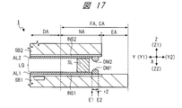
- FIG. 17 shows a schematic configuration of a cross section (YZ plane) of a sealing portion SL in a liquid crystal display device 1 according to a modification of the first embodiment.
- the regulating portions DM (DM1, DM2) are formed outside the sealing portion SL in the Y direction.
- the alignment films AL1 and AL2 are formed up to the inner ends E1 of the restriction portions DM1 and DM2, respectively.
- An end of the sealing portion SL in the direction Z2 is disposed on the first alignment film AL1 on the insulating film INS1.
- An end of the sealing portion SL in the direction Z1 is disposed on the second alignment film AL2 on the insulating film INS2.
- the restricting portion DM sets all regions as non-overlapping regions r2. Thereby, the adhesion performance of the sealing portion SL is ensured.
- FIG. 18 shows a schematic configuration of a cross section (YZ plane) of a sealing portion SL in a liquid crystal display device 1 of another modification.
- the regulating portion DM1 and the regulating portion DM2 are formed inside the sealing portion SL in the Y direction so as to overlap in a partial region (overlapping region r1).
- the restricting portions DM1 and DM2 have a non-overlapping area r2 on the inner end E1 side and an overlapping area r1 on the outer end E2 side.
- the sealing portion SL and the restricting portion DM are arranged so as to overlap in a partial area (overlapping area r1).
- the width for arranging the elements including the regulating portion DM and the sealing portion SL in the Y direction is reduced as a whole. Therefore, the width of the non-display area NA can be made shorter, and the frame area FA and the like can be made narrower. That is, this configuration is selected in consideration of the viewpoint of giving priority to the narrow frame configuration over the adhesive performance of the sealing portion SL.
- this configuration is selected in consideration of the viewpoint of giving priority to the narrow frame configuration over the adhesive performance of the sealing portion SL.
- the adhesion performance of the sealing portion SL is ensured by a region of the sealing portion SL that does not overlap with the restriction portion DM.
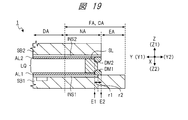
- FIG. 19 shows a schematic configuration of a cross section (YZ plane) of a sealing portion SL in a liquid crystal display device 1 of another modification.
- the regulating portion DM1 and the regulating portion DM2 are formed so as to overlap in a part of the region (overlapping region r1) outside the sealing portion SL in the Y direction.
- the restricting portions DM1 and DM2 have a non-overlapping area r2 on the outer end E2 side and an overlapping area r1 on the inner end E1 side.
- This configuration is also selected from the viewpoint of giving priority to the narrow frame configuration, and the same effect can be obtained.
- the end in the Z direction of the sealing portion SL is bonded to the alignment films AL1 and AL2.
- the material and the like of the sealing portion SL are selected in consideration of the adhesion performance with the alignment film varnish.
- the regulating portion DM can improve the unevenness of the end shape of the alignment film (the alignment films AL1 and AL2), and can reduce the size of the device and achieve high-density mounting. Can contribute.
- the uneven region at the end of the alignment film can be reduced, and the width of the region including the uneven region and the regulating portion can be suppressed. Therefore, for example, in the ratio of the display area DA and the non-display area NA (or the frame area FA or the circuit area CA) in the area of the front surface of the device, the display area DA can be increased and the non-display area NA can be reduced. .
- a narrow frame configuration or the like can be realized.
- the regulation part DM and the like can be formed by using the ink jet method, the production can be performed with a small number of steps, at low cost, and in a short time.
- Embodiment 2 A liquid crystal display device according to Embodiment 2 of the present invention will be described with reference to FIGS.
- a patterning method is used as a method for forming a restriction portion.
- components different from the first embodiment in the second embodiment will be described.
- FIG. 24 shows a schematic configuration of a cross section (YZ plane) of a main part of a mounting configuration example including a regulating part DM in the liquid crystal display device 1 according to the second embodiment.
- the configuration in FIG. 24 shows an example of a mounting configuration in a case where the restricting portion DM is formed by a general patterning method using a mask, etching, or the like, instead of the inkjet method. In the patterning method, an etching device or the like is used as a manufacturing device.
- the transistor TR has the insulating film INS21.
- the insulating film INS21 is formed over the display area DA, the non-display area NA, and the extension area EA.
- the insulating film INS21 serving as a base the insulating film INS22 and the insulating film INS23 are provided as two insulating films in order from the lower side to the upper side in the Z direction.
- the insulating film INS22 is provided over the insulating film INS21.
- the insulating film INS22 is a flattening film, and is particularly formed of an organic insulating film.
- the insulating film INS22 is formed by patterning over a part of the display area DA, the non-display area NA, and the extension area EA (the area from the end of the second substrate SB2 to the position Ya outside).
- an insulating film INS23 is formed by patterning.
- the insulating film INS23 is particularly formed of an organic insulating film.
- the insulating film INS23 is formed over the display area DA, the non-display area NA, and the extension area EA.
- the insulating film INS21 of the base and the first electrode EL1 are provided.
- these two layers of insulating films are provided between the pixel electrodes EP.
- the regulation part DM1 is formed by patterning two insulating films based on this configuration.
- the upper surface of the insulating film INS21 is referred to as a first surface sf1.
- a restricting portion DM1 is formed by patterning two insulating films (insulating films INS22 and INS23). That is, the restriction portion DM1 is formed on the side surfaces of the insulating films INS22 and INS23.
- the groove portions GR, the terminal portions EE, and the like are formed by patterning the insulating films INS22 and INS23.
- a groove GR is formed on the inner end E1 side of the regulating portion DM.
- the groove portion GR is a portion that is recessed below the height position of the upper surface of the insulating film INS23.
- the groove part GR extends along the X direction in accordance with the inner end part E1.
- a groove GR is required for forming the inner end E1 of the regulating portion DM1.
- the width of the groove GR in the Y direction is indicated by a width WG.
- the depth of the groove GR corresponds to the thickness (t1 + t2) obtained by adding the thickness t1 of the insulating film INS22 and the thickness t2 of the insulating film INS23.
- the alignment film AL1 is formed on the insulating film INS23 so as to cover the pixel electrode EP (first electrode EL1).
- the end of the alignment film AL1 falls from the upper surface of the insulating film INS23 to the surface of the insulating film INS21 in the groove GR, and is stopped by the inner end E1 of the regulating portion DM.
- the height relationship between elements is as follows.
- the first surface sf1 of the insulating film INS21 is used as a reference.
- the thickness of the insulating film INS22 is defined as a thickness t1
- the thickness of the insulating film INS23 is defined as a thickness t2
- the thickness of the alignment film AL1 is defined as a thickness t3.
- the height (thickness) of the regulating portion DM1 is height h1
- the height of the alignment film AL1 is height h2.
- the height of the alignment film AL1 in the groove portion GR is defined as a height h3.
- the height h1 is the sum of the thicknesses of the two insulating films (t1 + t2).
- the height h2 is a total value (t1 + t2 + t3) obtained by adding the thickness t3 to the total.
- the height position of the lower ground surface (surface sf3) of the alignment film AL1 is the same as the height position of the upper surface (surface sf4) of the regulating portion DM1. Therefore, the height h2 is larger than the height h1 (h2> h1). Further, in order to function as the regulating portion DM1, the height h3 is set to be smaller than the height h1 (h3 ⁇ h1). In summary, h2> h1> h3.
- the groove portion GR is particularly formed at a position near the sealing portion SL in the Y direction, and the region of the groove portion GR overlaps with the region of the sealing portion SL in plan view. .
- a part of the lower end of the sealing portion SL in the Z direction is formed so as to enter the groove portion GR.
- the region of the regulating portion DM1 in the Y direction is such that a part of the region on the inner end portion E1 side is an overlapping region r1 overlapping the sealing portion SL, and the other outer end portion E2 side. Is a non-overlapping region r2.
- the insulating film INS23 on the upper surface (the surface sf4) of the regulating portion DM1 is in direct contact with the end of the sealing portion SL.
- the alignment film AL1 is in contact with the end of the sealing part SL.
- the area including the regulating part DM1, the sealing part SL, and the groove GR is the non-display area NA.
- the restriction portion DM2 may be formed by a patterning method in the same manner as described above.
- the video signal lines WR1 and WR2 and the shield electrode SE are formed in the non-display area NA.
- the video signal lines WR1, WR2 and the shield electrode SE are formed at positions inside the sealing portion SL and the groove portion GR.
- This shield electrode SE is formed in the same layer as the common electrode EC on the insulating film INS22, and is covered with the insulating film INS23.
- the invention is not limited thereto, and the shield electrode SE may be formed so as to come out of the groove GR and come into contact with the alignment film AL1 or the like.
- FIG. 25 shows a schematic configuration of the groove GR and the restricting portion DM1 of FIG. 24 in a plan view according to the second embodiment.
- FIG. 25 shows a main region 251 of the alignment film AL1, a region 252 of the groove GR, and a regulating portion DM1.
- the region 251 corresponds to the region with the height h2 in FIG.
- the region 252 corresponds to the region with the height h3 in FIG. 25 shows a case where the regulating portion DM1 has an uneven shape on the inner end portion E1 side as in FIG. 7, but is not limited to this, and various shapes are possible.
- FIG. 25 shows the rebound uneven area 253 and the width M3 of the uneven area 253.
- the total width (H1 + M3) obtained by combining the width M3 of the uneven region 253 and the width H1 of the regulating portion DM1 can be reduced.
- the width W1 of the irregularities of the regulating portion DM1 is set to W1 ⁇ 100 ⁇ m, as in the first embodiment.
- the width WG of the groove GR is set to 200 ⁇ m or less (WG ⁇ 200 ⁇ m).
- the width WG of the groove GR is, for example, about twice as large as the interval pt5 for forming the unevenness (WG ⁇ pt5 ⁇ 2).
- the regulating portion DM can improve the unevenness of the end shape of the alignment film (the alignment film AL1). It can contribute to miniaturization and high-density mounting. That is, according to the second embodiment, a narrow frame configuration or the like can be realized.
- a patterning method since a patterning method is used, a plurality of steps such as masking and etching are required at the time of formation. However, it is possible to precisely control the uneven shape of the regulating portion DM by patterning.
- Embodiment 3 A liquid crystal display device according to Embodiment 3 of the present invention will be described with reference to FIGS. Hereinafter, components different from the first and second embodiments in the third embodiment will be described.
- the liquid crystal display device according to the third embodiment has a restricting portion having another shape.
- regulating section DM (DM1, DM2) having a specific shape is provided on the SB2 side.
- the regulating portion DM having this unique shape has a plurality of regions having gaps as shown in FIG. 27 described later.
- FIG. 26 shows a cross section (YZ) of the liquid crystal display device 1 according to the third embodiment, which relates to the regulating portions DM (DM1, DM2) of the lower regulating portion DM11, the alignment film AL (AL1, AL2), the sealing portion SL, and the like. 2) shows a configuration example of (surface).
- FIG. 27 shows an example of the configuration of a regulating portion having a unique shape, particularly with respect to the regulating portion DM11 on the first substrate SB1 side in FIG.
- FIG. 27A shows a schematic configuration of the regulating section DM31 of the first configuration example
- FIG. 27B shows a schematic configuration of the regulating section DM32 of the second configuration example.
- the first restricting unit DMA includes a restricting unit DM31 or a restricting unit DM32 as shown in FIG.
- FIG. 28 shows a detailed configuration in plan view of the regulating section DM31 and the like of the first configuration example.
- FIG. 29 shows a detailed configuration in plan view of the regulating portion DM32 and the like of the second configuration example.
- FIG. 30 shows a detailed configuration of the restricting portion DM33 of the first modification example in plan view with respect to the restricting portion DM31 of the first configuration example.
- FIG. 31 shows a detailed configuration in plan view of a regulating portion DM34 of a second modified example related to the regulating portion DM32 of the second configuration example.
- FIGS. 32 to 38 show the configuration of the restricting portion of various modifications in the third embodiment.
- FIG. 39 shows a configuration of a regulating unit DM30 and the like of a comparative example with respect to the third embodiment.
- the regulating portion DM and the sealing portion SL are arranged so as to overlap. Therefore, the overall width of the area required for the regulation part DM and the sealing part SL is small, and the width of the non-display area NA can be reduced, which is advantageous for a narrow frame configuration.
- the cross-sectional configuration of the restricting portion DM and the sealing portion SL in the third embodiment is not limited to this configuration example, and the various configuration examples described in the first embodiment and the like are similarly applicable.
- FIG. 39 shows a configuration example of a regulating portion DM30 related to a partial region 390 on the lower side of the frame region in the liquid crystal display device of the comparative example.
- This restriction part DM30 is linear along the X direction, similarly to the restriction part 201 of FIG.
- the width HS0 is, for example, 400 ⁇ m.
- the region of the sealing portion SL0 there is a region of the regulating portion DM30 having a constant width H30 in the Y direction so as to overlap in a plan view.
- the width H30 is, for example, 200 ⁇ m.
- On both sides of the inner end portion E1 and the outer end portion E2 of the regulating portion DM30 there are regions of the sealing portion SL0 having the width L30.
- the width L30 of this region is, for example, 100 ⁇ m.
- the regulating portion DM30 is formed on the insulating film of the first substrate. Thereafter, although not shown, an alignment film is formed on the inner end portion E1 side of the regulating portion DM30.
- the alignment film varnish is applied in the main direction 401 (direction Y2). The flow of the alignment film varnish is blocked at the inner end E1 side of the regulating portion DM30, and rebounds.
- the uneven region M30 indicates the concept of unevenness at the edge of the alignment film.
- a sealing portion SL0 is formed in a region of the width HS0 above the members in the Z direction. At that time, the sealing portion material is in close contact with and adheres to the alignment film in the region on the inner end portion E1 side, the insulating film in the region on the outer end portion E2 side, and the regulating portion DM30.
- the unit area U0 and the like are shown for the purpose of comparison described below.
- the unit area U0 has a width HS0 in the Y direction and a unit length UL0 in the X direction.
- the unit length UL0 is, for example, 100 ⁇ m.
- the restriction part area Q1 is the area of the restriction part DM30.
- the non-regulating portion area Q2 is the area of the portion of the alignment film or the insulating film other than the regulating portion DM30, that is, the portion of the width L30.
- FIG. 27 in the liquid crystal display device 1 according to the third embodiment, a plan view of the restricting portion DM31 of the first configuration example and the restricting portion DM32 of the second configuration example with respect to a partial area 270 on the lower side of the frame area FA.
- the schematic configuration of is shown.
- the restricting portion DM31 of the first configuration example can be regarded as a mode in which a gap is provided between each circular region in the configuration example of FIG.
- the regulating portion DM31 of the first configuration example has a plurality of circular regions RC1 in one row in the Y direction.
- a circular region may be described as a circle.
- the plurality of circular regions RC1 in one row are arranged at the position y31 which is the arrangement center position C1 in the Y direction. That is, the center point of each circular region RC1 is on the straight line at the position y31.
- the plurality of circular regions RC1 are arranged with a gap 51 between adjacent circles in the X direction.
- the gap 51 has a distance K1 in the X direction.
- the distance K1 is a distance between the nearest edges of two adjacent circular regions RC1.
- the distance K1 is, for example, 70 ⁇ m.
- Adjacent circles in the plurality of circles in one row are arranged at a predetermined interval k31.
- the interval k31 is a distance between the center points of the circles.
- One circular region RC1 has a diameter R31.
- the width H31 of the regulating portion DM31 in the Y direction is the same as the diameter R31 of the circular region RC1.
- the width H31 and the diameter R31 are the same as the width H30 of the comparative example, and are, for example, 200 ⁇ m.
- the sealing portion SL is arranged in a region having a constant width HS1 in the Y direction.
- the width HS1 is the same as the width HS0 of the comparative example, for example, 400 ⁇ m.
- the restricting portion DM31 is arranged to be included in the region of the width HS1 of the sealing portion SL in a superimposed manner.
- the innermost position (left side in the figure) of the width H31 of the regulating portion DM31 and the circular region RC1 is indicated by a line a31, and the outermost position (right side in the figure) is indicated by a line a32.
- the unit area U1 and the like are shown for the following comparative explanation.
- the unit area U1 has a width HS1 in the Y direction and a unit length UL1 in the X direction.
- the unit length UL1 is a distance between corresponding edges in two circles adjacent in the X direction, and is the same as a distance between the center points of the circles (interval k31), for example, 270 ⁇ m.
- the area of the unit region U1 is made up of a regulated area Q11 and a non-regulated area Q12.
- the restriction part area Q11 is the area of the circular area RC1 in the unit area U1.
- the unregulated portion area Q12 is an area other than the circular area RC1 in the unit area U1.
- the regulating portion DM32 of the second configuration example has a plurality of circular regions Rc1 in the first column and a plurality of circular regions Rc2 in the second column as a group of circles in the Y direction.
- the inner first group of circles is arranged at position y32
- the outer second group of circles is arranged at position y33.
- the configuration of the first row and the configuration of the second row are basically the same, but the arrangement positions of the circles in the X direction are different.
- the diameter R32 of the circles in each row is the same, for example, 100 ⁇ m.
- Adjacent circles in the plurality of circles in one row are arranged at a predetermined interval k32.
- the interval k32 is, for example, 275 ⁇ m.
- the positions of the circles in the X direction are staggered alternately.
- the circular region Rc2 in the second column is disposed at an intermediate position in the interval k32 between two circular regions Rc1 adjacent in the X direction in the first column.
- the restricting portion DM32 of the second configuration example can be regarded as a configuration in which a gap is provided between each circular region in the configuration example of FIG.
- the sealing portion SL is arranged in a region having a constant width HS2 in the Y direction.
- the width HS2 is the same as the widths HS1 and HS0, and is, for example, 400 ⁇ m.
- the regulating portion DM32 is disposed so as to be included in the region of the width HS2 of the sealing portion SL in a superimposed manner.
- the regulating portion DM32 formed by the two groups of circles has a width H32 in the Y direction.
- the width H32 is twice the diameter R32.
- the width H32 is the same as the widths H31 and HS30, and is, for example, 200 ⁇ m.
- the two rows of circle groups are arranged without a gap in the Y direction.
- the position y31 which is the arrangement center position C1 of the regulating portion DM32 is an intermediate position between the positions (y32, y33) in the two rows.
- the innermost position of the width H32 of the regulating portion DM32 is indicated by a line a31, and the outermost position is indicated by a line a32.
- a gap 52a is provided between two circles (circular regions Rc1 and Rc2) that are adjacent to each other in a diagonal direction to the X and Y directions in the entire two rows.
- the gap 52a has a distance K2.
- the distance K2 is, for example, 70 ⁇ m.
- Two circles adjacent to each other in the oblique direction are arranged at an interval G2.
- the interval G2 is a distance between the center points of the circles.
- the interval G2 is, for example, 170 ⁇ m.
- G2 K2 + R32.
- the oblique direction is a direction (third direction) intersecting the X direction and the Y direction in plan view.
- the unit area U2 and the like are shown for a comparative explanation described later.
- the unit area U2 has a width HS2 in the Y direction and a unit length UL2 in the X direction.
- the unit length UL2 is the distance between the corresponding edges of two circles adjacent in the X direction in one row of circle groups, and is the same as the distance between the circle center points (interval k32), for example, 275 ⁇ m.
- the area of the unit region U2 is made up of a restricted area Q21 and a non-restricted area Q22.
- the restriction portion area Q21 is the area of two circles (a circular region Rc1 and a circular region Rc2).
- the non-regulating portion area Q22 is an area other than two circles.
- the ink jet method can be applied to the restricting portions DM31 and DM32 in the third embodiment, similarly to the first embodiment, and a patterning method and the like can be applied similarly to the second embodiment. It is possible.
- the regulating portion DM2 on the second substrate SB2 side can also have the same configuration as the regulating portion DM1 on the first substrate SB1 side.
- the plurality of regions constituting the restriction portions DM31 and DM32 may be shifted or formed within a certain range with respect to the formation position or shape, for example, as in FIG. May have shaking.
- the restricting portion DM31 has an inner end E1 and an outer end E2 in the Y direction.
- Each end of the regulating portion DM31 has a roughly uneven shape along the X direction, as in the first embodiment.
- the inner end E1 is shown as a range from the center position y31 to the innermost line a31.
- the outer end E2 is shown as a range from the center position y31 to the outermost line a32.
- the inner end E1 is an end on the side mainly in contact with the end of the alignment film (the above-described alignment film AL1).
- the outer end E2 is an end opposite to the inner end E1, and is in contact with an alignment film end 601 which is a part of an end of the alignment film.
- a plurality of concave portions 41 and a plurality of convex portions 42 are formed at the inner end portion E1.
- the convex portion 42 is configured by a semicircular portion on the left side from the center of the circular region RC1.
- the concave portion 41 is configured as a region between the convex portions 42 adjacent in the X direction, and includes the gap 51.
- the plurality of convex portions 42 and the circular region RC1 are arranged at the above-described interval k31.
- the plurality of recesses 41 and the plurality of gaps 51 are similarly arranged at an interval k31.
- a plurality of concave portions 43 and a plurality of convex portions 44 are formed on the outer end portion E2 side.
- the convex portion 44 is constituted by a semicircular region on the right side from the center of the circular region RC1.
- the concave portion 43 is configured as a region between the convex portions 44 adjacent in the X direction, and includes the gap 51.
- the shape of the regulating portion DM31 is symmetrical with respect to the center line of the position y31, but is not limited thereto, and may be asymmetrical.
- the plurality of circles (circular regions RC1) have a perfect circular shape with the same diameter R31, but are not limited to this, and may have another shape, such as an elliptical shape, within a range satisfying the conditions described later.
- the sealing portion SL is arranged in the region of the width HS1, and the innermost position is indicated by a line b31, and the outermost position is indicated by a line b32.
- the region having the width L31 is a region from the line a31 to the line b31.
- the region having the width L32 is a region from the line a32 to the line b32.
- the widths L31 and L32 are the same, for example, 100 ⁇ m. Similar to the sealing portion SL0 of the comparative example, the sealing portion SL is in contact with the alignment film AL1, the regulating portion DM1 (DM31), and the insulating film INS1 above the insulating film INS1 in FIG. Be placed.
- FIG. 28 also shows an alignment film end 601 which is a part of the end of the first alignment film AL1 whose spread is restricted by the restriction portion DM31.
- Black arrows indicate the outline of the flow of the alignment film varnish.
- the alignment film varnish hits the uneven shape of the inner end portion E2 in the direction Y2, so that the rebound unevenness is reduced.
- the alignment film varnish enters the gap 51 so as to hit the circular region RC1 and avoid the region.
- the alignment film varnish hits the circular region RC1 (the convex portion 42), enters the concave portion 41, and proceeds to the gap 51.
- the alignment film varnish passes through the gap 51 in the direction Y2 and proceeds to the concave portion 43 on the outer end E2 side.
- the alignment film end 601 advances to near the center position y31 as shown in the drawing, and is stopped just slightly outside the position y31.
- the alignment film end 601 is stopped near the position y31 of the gap 51.
- the position y31 of the gap 51 is narrowest in the X direction like the distance K1, and the surface tension is particularly apt to work.
- the side surface of the circular region RC1 stands roughly in the Z direction, for example, similarly to the cross section of FIG.
- the cross section (YZ plane) of the EE line passing through the circular region RC1 of the restricting portion DM31 has, for example, a concave shape as in FIG. 5, but is not limited thereto, and may have a convex shape as in FIG. It may be.
- the alignment film AL1 including the alignment film end portion 601 and the sealing portion on the insulating film INS1.
- SL has a cross section.
- the alignment film varnish is drawn into the regulating portion DM31 through the gap 51.
- the end of the alignment film goes only up to the position of the straight line of the inner end E1.
- the end of the alignment film goes only up to the position of the line b1 of the inner end E1.
- the orientation film varnish is drawn more in the direction Y2 than those configurations. Therefore, in the first configuration example, the width of the uneven area M31 can be reduced as compared with the uneven areas of those configurations.
- the uneven region M31 protrudes inside the line b31 of the sealing portion SL, but is not limited to this, and may be within the region of the width L31 of the sealing portion SL.
- the alignment film end 601 is stopped near the center position y31.
- the alignment film end 601 can be roughly set within the range of the width H31 of the regulating portion DM31. What is necessary is just to be formed.
- the regulating portion DM31 of the first configuration example in the third embodiment since the alignment film varnish is drawn through the gap 51, the rebound of the alignment film varnish in the direction Y1 is suppressed, and the uneven region M31 is reduced. Can be reduced. At the same time, the expansion of the alignment film varnish outward in the direction Y2 from the sealing portion SL (line b32) is regulated. Thereby, the width of the non-display area NA can be reduced, which is advantageous for a narrow frame configuration.
- the ratio of the regulating portion area Q11 in the unit area U1 is small, and the ratio of the non-regulating portion area Q12 is large, because the regulating portion DM31 has the shape of a circle and the gap 51 is provided. That is, the ratio of the regulating portion area Q11, which is the area where the sealing portion SL contacts the regulating portion DM31, is small.
- the adhesion performance of the sealing portion SL can be maintained or improved, and peeling or the like can be prevented.
- FIG. 28 shows the flow of the alignment film material in a plan view, but the flow of the alignment film material in a cross section in the Z direction (for example, a cross section of the EE line or a cross section of the FF line) is considered.
- the regulating portion DM31 functions as an obstacle to stop the spread of the alignment film material.
- the height of the alignment film varnish may be within the height of the regulating portion DM31, or may be higher than the height of the regulating portion DM31.
- the height of the alignment film after being formed by baking or the like may be in the vicinity of the regulating portion DM31, within the height of the regulating portion DM31, or may be higher than the height of the regulating portion DM31.
- the regulating part DM32 has a plurality of circular regions Rc1 in the first inner row V1 and a plurality of circular regions Rc2 in the outer second row V2 as a group of circles in two rows.
- the entire two rows of the regulating portions DM32 are arranged at the position y31 which is the arrangement center position C1, and have a width H32.
- the line a31 corresponds to the left end of the circle group in the first column V1
- the line a32 corresponds to the right end of the circle group in the second column V2.
- the sealing portion SL has regions of widths L31 and L32 on both sides of the region of width H32 of the regulating portion DM32 in the region of width HS2 in the Y direction.
- the widths L31 and L32 in the second configuration example are the same as the widths L31 and L32 in the first configuration example.
- the inner end E1 is a part of the circle group of the first row V1 with respect to the center position y31
- the outer end E2 is a part of the circle group of the second row V2 with respect to the center position y31.
- the restricting portion DM32 has an uneven shape roughly along the X direction at each end in the Y direction.
- a concave portion 41 and a convex portion 42 are formed on the inner end E1 side.
- a concave portion 43 and a convex portion 44 are formed on the outer end portion E2 side.
- the convex portion 42 is configured by a group of circles in the first row V1.
- the concave portion 41 is formed between the convex portions 42 adjacent in the X direction.
- the convex portion 44 is formed by a group of circles in the second row V2.
- the concave portion 43 is formed between the convex portions 44 adjacent in the X direction.
- the plurality of circular regions Rc1 are arranged at an interval k32.
- the plurality of circular regions Rc2 are arranged at an interval k32.
- the circular region Rc2 of the second column V2 is arranged at an intermediate position with respect to the position of two adjacent circular regions Rc1 of the first column V1. In the entire two rows, the circular region Rc1 and the circular region Rc2 that are adjacent in the X direction are arranged at a half interval of the interval k32.
- the regulating portion DM32 has two circles (circular regions Rc1 and Rc2) adjacent to each other in a diagonal direction (for example, the direction D32) with respect to the X direction and the Y direction in the entire two rows. Two circles in the oblique direction are arranged at an interval G2, and have a gap 52a between the two circles.
- the gap 52a has a distance K2.
- One recess 41 is connected to two gaps 52a having different directions.
- the restricting portion DM32 has a gap 52b in the X direction corresponding to the gap 52a.
- the gap 52b has a distance K2b. In this example, there is a gap 52b in the X direction, but a configuration without the gap 52b is also possible.
- FIG. 29 also shows an alignment film end 602 that is a part of the end of the first alignment film AL1 whose expansion is restricted by the restriction portion DM32.
- Black arrows indicate the outline of the flow of the alignment film varnish.
- the alignment film varnish hits the circular region Rc1 in the first row V1 in the direction Y2 and enters the concave portion 41.
- the alignment film varnish hits the circular region Rc2 of the second row V2 from the concave portion 41 and proceeds toward the two gaps 52a.
- the alignment film varnish passes through each gap 52a and proceeds to the concave portion 43 on the outer end E2 side.
- surface tension acts between the circular region Rc1 and the circular region Rc2 with the alignment film varnish.
- the gap 52a near the position y31 is the narrowest as the distance K2, and the surface tension is likely to work.
- the alignment film varnish advances to near the position y31 of the gap 52a, is stopped by surface tension, and is formed as an alignment film end 602 (602a, 602b).
- the alignment film end 602a indicates a portion formed in one gap 52a
- the alignment film end 602a indicates a portion formed in the other gap 52a.
- the two alignment film ends 603a and 603b may join as one alignment film end.
- the alignment film end 602 is stopped at the two gaps 52a near the center position y31.
- the present invention is not limited to this, and the alignment film end 602 can be roughly set within the width H32 of the regulating portion DM32. What is necessary is that the alignment film end 602 is formed.
- the alignment film end 602 may be formed, for example, near the position y33 or near the line a32 within the range of the outer end E2.
- the regulating portion DM32 of the second configuration example since the alignment film varnish is drawn through the gap 52a, the rebound of the alignment film varnish in the direction Y1 is suppressed, and the uneven region M32 can be reduced. At the same time, the expansion of the alignment film varnish outward in the direction Y2 from the sealing portion SL (line b32) is regulated. Thereby, the width of the non-display area NA can be reduced. Further, according to the restricting portion DM32, the ratio of the restricting portion area Q21 in the unit area U2 is small, and the ratio of the non-restricting portion area Q22 is large, since the shape of the circle group is provided and the gap 52a is provided. That is, the ratio of the regulating portion area Q21, which is the area where the sealing portion SL contacts the regulating portion DM32, is small. Thereby, the adhesive performance by the sealing portion SL can be maintained or improved.
- the second configuration example is different from the first configuration example in that the direction of the gap is oblique to the direction Y2, and the concave portion 41 and the concave portion 43 are widened.
- the alignment film varnish can be blocked while drawing the alignment film varnish into the regulating portion DM32.
- FIG. 30 shows a plan view configuration of the regulating portion DM33 of a modification (hereinafter referred to as a first modification) relating to the first configuration example and the second configuration example.
- the restricting part DM33 is configured as a first way of understanding, as a group of circles in one row, and the center line where the circle groups are arranged has a zigzag shape.
- Two circular regions RC1 adjacent in the X direction are arranged at different positions y32 and y33 in the Y direction.
- the distance between the position y32 and the position y33 is defined as a distance Y33.
- the distance Y33 is smaller than the diameter R33 of the circular area RC1.
- the distance Y33 is set to a half (ie, a radius) of the diameter R33.
- the width HS3 of the sealing portion SL and the width H33 of the regulating portion DM33 are smaller than the width HS1 and the width H31 of the first configuration example by the distance Y33.
- a concave portion 41 and a convex portion 42 are formed on the inner end E1 side.
- a concave portion 43 and a convex portion 44 are formed on the outer end portion E2 side.
- the concave portion 41 on the inner end portion E1 side and the concave portion 43 on the outer end portion E2 side are configured as smaller concave portions.
- the restricting portion DM33 is configured by two rows of circle groups, the first row is arranged at the position y32, and the second row is arranged at the position y33.
- the circle group in the first row and the circle group in the second row are alternately arranged with a shift.
- the circle groups in each row are arranged at an interval k33 in the X direction. In the Y direction, the outer end of the first row of circles is at position y33 and the inner end of the second row of circles is at position y32.
- Two circular regions RC1 adjacent in the oblique direction are arranged at an interval G3, and have a gap 53a between the two circular regions RC1.
- the gap 53a has a distance K3.
- One recess 41 is connected to two gaps 53a having different directions.
- the restricting portion DM33 has a gap 53b in the X direction corresponding to the gap 53a.
- the gap 53b has a distance K3b.
- FIG. 30 similarly shows the unit area U3.
- the unit area U3 has a width HS3 and a unit length UL3.
- the regulating portion area is the area of the two circular regions RC1
- the non-regulating portion area is the area other than the two circular regions RC1.
- the alignment film varnish hits the first row of circular regions RC1 and enters the concave portion 41 in the direction Y2, hits the second row of circular regions RC1, and proceeds to the two gaps 53a.
- the alignment film varnish proceeds to the concave portion 43 on the outer end E2 side through the two gaps 53a.
- the alignment film varnish is stopped as the alignment film end 603 (603a, 603b) by the surface tension between the circular regions RC1 in the gap 53a near the arrangement center position C1, for example.
- the present invention is not limited to this, and the alignment film end 603 may be formed within the range of the width H33 of the regulating portion DM33.
- the alignment film end 603 may be formed near the position y33 or near the line a32.
- FIG. 31 shows a plan view of the configuration of the restricting portion DM34 of a modification (hereinafter referred to as a second modification) related to the second configuration example.
- the restricting portion DM34 is composed of two rows of circle groups similarly to the restricting portion DM32, and further has a gap 310 between the two rows of circle groups in the Y direction.
- the gap 310 has a distance Y34 in the Y direction.
- the circle in the first row V1 (circular region Rc1) and the circle in the second row V2 (circular region Rc2) have the same diameter R34.
- the circle group in the first row V1 and the circle group in the second row V2 are arranged at an interval k34.
- the circle group in the first row V1 is arranged in the region from line a31 to line a33.
- the circle group in the second row V2 is arranged in the region from the line a34 to the line a32.
- the gap 310 is a region from the line a33 to the line a34.
- the inner end E1 is an area of a circle group in the first row V1
- the outer end E2 is an area of a circle group in the second row V2.
- the concave portion 41 and the convex portion 42 are formed by the circular region Rc1 and the gap 310 in the first row V1.
- a concave portion 43 and a convex portion 44 are formed by the circular region Rc2 and the gap 310 in the second row V2.
- the sealing portion SL is arranged in a region of the width HS4.
- the restricting portion DM34 is arranged in a region of the width H34.
- the width H34 is R34 + Y34 + R34. Regions of widths L31 and L32 are provided on both sides of the region of the regulating portion DM34.
- Two circles (circular regions Rc1 and Rc2) adjacent in an oblique direction (for example, the direction D34) are arranged at an interval G4, and have a gap 54a between the two circles (circular regions Rc1 and Rc2).
- the gap 54a has a distance K4.
- the restricting portion DM34 has a gap 54b in the X direction, and the gap 54b has a distance K4b. Note that a configuration without the gap 54b is also possible.
- FIG. 31 similarly shows the unit area U4.
- the unit area U4 has a width HS4 and a unit length UL4.
- the regulating portion area is the area of the two circular regions Rc1 and Rc2
- the non-regulating portion area is the area other than the two circular regions Rc1 and Rc2.
- the alignment film varnish hits the circular region Rc1 of the first row V1 in the direction Y2 and enters the concave portion 41.
- the alignment film varnish hits the circular region Rc2 of the second row V2 from the concave portion 41 and proceeds toward the two gaps 54a.
- the alignment film varnish proceeds to the concave portion 43 on the outer end portion E2 side through each gap 54a.
- the alignment film varnish is removed by the action of surface tension between two circles (circular regions Rc1 and Rc2) that are adjacent to each other in the oblique direction, for example, in the gap 54a near the arrangement center position C1. , 604b).
- the present invention is not limited thereto, and the alignment film end 604 may be formed substantially within the range of the width H34 of the regulating portion DM34.
- the width H34 of the regulating portion DM34 is wider, and the alignment film varnish including the gap 310 in the Y direction is more drawn in, so that the uneven region M34 can be further reduced.
- the shape conditions such as dimensions are as follows. It is.
- the distance K1 is 70 ⁇ m.
- the regulating part DM31 has a shape having a gap 51 so as to satisfy this condition.
- the surface tension sufficiently acts in the gap 51 between the circular regions RC1, and the alignment film end 601 is formed near the position y31.
- the alignment film end 601 does not protrude at least from the line b32 of the sealing portion SL.
- the position and the like of the alignment film end 601 can be adjusted by designing to adjust the dimension and the like of the distance K1 of the gap 51.
- This condition is a condition related to the distance K2 of the gap 52a for forming the alignment film end 602 within the range of the width H32 of the regulating portion D32, particularly, near the position y31 of the gap 52a as shown in FIG. .
- This condition is the same as in the above equation 3, and 0 ⁇ K2 ⁇ 120 ⁇ m.
- the distance K2 is 70 ⁇ m.
- the restricting portion DM32 has a shape having a gap 52a so as to satisfy this condition.
- the surface tension sufficiently acts in the gap 52a between the oblique circular regions Rc1 and Rc2, and the alignment film end 602 is formed near the position y31.
- the alignment film end 602 does not extend outward from at least the line b32 of the sealing portion SL.
- the position and the like of the alignment film end 602 can be adjusted by designing to adjust the dimension and the like of the distance K2 of the gap 52a.
- the regulating portion DM31, the alignment film (first alignment film AL1), and the sealing portion SL in FIG. 28 can be formed as follows using an inkjet method.
- (1) It is assumed that up to the insulating film INS1 of the first substrate SB1 in FIG. 26 is formed.
- the ink jet device applies the regulating portion material to the region 260 (corresponding width HS1) on the surface of the insulating film INS1 by discharging droplets of the regulating portion material (varnish).
- a plurality of circular regions RC1 having the gaps 51 in the restricting portion DM31 can be formed by controlling the interval of ejection of the droplets from the ink jet device, the pressure, and the like.
- (3) The manufacturing apparatus solidifies the regulating portion material on the first substrate SB1 by drying or the like. Thereby, the regulating portion DM31 is formed.
- the inkjet device applies the alignment film varnish of the first alignment film AL1 in the Y direction (for example, the direction Y2) to a region inside the regulating portion DM31 in the direction of the droplet. It is applied by ejection. At this time, as described above, the unnecessary spread of the alignment film varnish is restricted by the restriction portion DM31, and the alignment film end 601 is formed within the range of the restriction portion DM31.
- the manufacturing apparatus solidifies the alignment film varnish on the first substrate SBI by drying or the like.
- the manufacturing apparatus reacts the regulating portion material and the alignment film varnish on the first substrate SB1 by firing or the like.
- the manufacturing apparatus performs an alignment process on the first alignment film AL1 using, for example, an optical alignment method.
- the restriction portion and the alignment film on the second substrate SB2 side can be similarly formed.
- the step of forming the sealing portion SL between the first substrate SB1 and the second substrate SB2 is as follows. (8-1) First, in the region of the width HS1 on the first substrate SB1, on the upper side in the Z direction of the regulating portion DM31, the insulating film INS1, and the first alignment film AL1, a sealing material such as an ultraviolet curable material is used. An adhesive is placed. (8-2) In a vacuum environment, the liquid crystal is dropped into the frame made of the sealing portion material of the first substrate SB1. (8-3) The second substrate SB2 is placed on the upper side of the first substrate SB1, the sealing portion material and the like.
- the sealing portion material between the first substrate SB1 and the second substrate SB2 is pushed from above and below in the Z direction, and the respective members adhere to each other.
- the sealing portion material is cured by irradiating the sealing portion material with ultraviolet rays. Thereby, the sealing portion SL is formed.
- the sealing portion material is brought into close contact with the upper surface and side surfaces of the regulating portion DM31, the upper surface of the first alignment film AL1, the alignment film end portion 601, the upper surface of the insulating film INS1, and the like.
- the adhesion performance of the sealing portion SL will be described by comparing the regulating portion DM30 of the comparative example in FIG. 39 with the regulating portion DM31 of the first configuration example and the regulating portion DM32 of the second configuration example in FIG.
- the adhesion strength between the sealing material and another member that is, the regulating portion DM30, the alignment film, and the insulating film
- the adhesion strength of the regulating portion DM31 of the first configuration example is about 1.42
- the adhesion strength of the regulating portion DM32 is about 1.72.
- the adhesion strength of the sealing portion SL is roughly proportional to the area of the sealing portion SL not touching the regulating portion, of the area of the entire region of the sealing portion SL in plan view. Of the total area of the sealing portion SL, the larger the area of the region touching the regulating portion, the lower the adhesion strength. That is, the adhesion strength is roughly determined according to the ratio of the area of the restricting portion and the area of the non-regulating portion in the sealing portion forming region in plan view. In the third embodiment, depending on the design of the material and the like, the adhesion strength of the non-regulating portion such as the alignment film and the insulating film is higher than that of the regulating portion DM with respect to the adhesion performance of the sealing portion SL. Therefore, as described above, the lower the ratio of the area of the restriction portion in the sealing portion formation region, the higher the adhesion strength as a whole.
- the regulating portion area Q1 corresponds to the area where the sealing portion SL0 contacts the regulating portion DM30.
- the non-regulating portion area Q2 corresponds to an area where the sealing portion SL0 does not touch the restricting portion DM30, and is a region where the alignment film or the insulating film is disposed.
- the adhesion strength of the sealing portion SL0 is determined according to the ratio between the regulating portion area Q1 and the non-regulating portion area Q2 in the unit region area Q0.
- the ratio of the unregulated portion area Q2 to the unit region area Q0 is 0.5.
- the configuration of the restricting portion DM is changed from a linear shape as in the comparative example to a circle group having a gap as in the first configuration example.
- the ratio of the area where the sealing portion SL contacts the regulating portion DM (the regulating portion area Q1) can be reduced as compared with the comparative example, and the sealing portion SL does not touch the regulating portion DM.
- the ratio of the area (the non-regulating portion area Q2) can be increased.
- the adhesion strength by the sealing portion SL that is, the bonding performance can be improved.
- the restriction area Q11 is the area of a circular region RC1 having a diameter R31 (for example, 200 ⁇ m), and is ⁇ ⁇ 100 ⁇ m ⁇ 100 ⁇ m ⁇ 0.0314 mm 2 .
- the ratio of the regulating portion area Q1 in the unit region U1 is 0.0314 mm 2 ⁇ 0.108 mm 2 ⁇ 0.29.
- the ratio of the non-regulating portion area Q2 in the unit region U1 is about 0.71.
- the ratio of the regulating portion area Q21 in the unit region U2 is 0.0157 mm 2 ⁇ 0.11 mm 2 ⁇ 0.14.
- the ratio of the non-regulating portion area Q22 in the unit region U2 is about 0.86.
- the alignment film and an insulating film as two types of members other than the regulating portion DM, which are in contact with the sealing portion material.
- the alignment strength between the alignment film and the insulating film hardly changes with respect to the adhesion strength with the sealing portion material. Therefore, in the above estimation calculation, the area of the non-regulating portion is the area of one region that does not depend on the difference between the alignment film and the insulating film.
- the alignment film and the insulating film may have different adhesion strengths with respect to the sealing portion.
- the adhesion strength may be calculated using each of the alignment film region area and the insulating film region area, and the area of each member may be designed.
- the alignment film end 601 is near the center position y31.
- the area of the alignment film region and the area of the insulating film region are substantially the same.
- the alignment film end 605 is near the line a32 of the outer end E2.
- the area of the alignment film region is larger than the area of the insulating film region.
- the area of the alignment film region and the area of the insulating film region can be designed according to the position of the edge of the alignment film in the sealing portion forming region.
- the adhesion strength with the sealing portion can be calculated according to the area of each of these members. For example, depending on the material design, if the adhesion strength between the sealing portion material and the insulating film is higher than the adhesion strength between the sealing portion material and the alignment film, the insulating film region area is increased as much as possible. What is necessary is just to design the position of the edge part of an alignment film.
- the position of the alignment film end 601 may be set to a position close to the inner end E1 side.
- the edge of the alignment film is so formed as to have as large an area of the alignment film region as possible. You only need to design the position.
- the position of the alignment film end 601 may be set to a position close to the outer end E2 side.
- FIG. 32 illustrates a plan view configuration of the restricting portion DM35 of another modification (hereinafter, referred to as a third modification) related to the first configuration example.
- the restricting portion DM35 has the same shape as the restricting portion DM31.
- the alignment film end 605 extends in the Y direction to a position near the outermost line a32 of the outer end E2 and is stopped. I have.
- the distance of the gap 51 of the third modification is wider than the distance K1 of the gap 51 of the first configuration example.
- the alignment film varnish is drawn into the regulating portion DM35 through the gap 51 more, the uneven region M35 can be further reduced.
- FIG. 32 illustrates a plan view configuration of the restricting portion DM36 of another modified example (hereinafter, referred to as a fourth modified example) of the first configuration example.
- the restricting portion DM36 has a different configuration point in which the alignment film end 606 extends in the Y direction beyond the line a32 of the outer end E2, and further extends to a position near the outer position y36.
- the alignment film end 606 is located inside the line b32 outside the sealing portion SL.
- One alignment film end 606 is held between two adjacent circular regions RC1 in the X direction and between the slopes on the outer end E2 side by surface tension.
- the end of the alignment film may be out of the range of the width of the regulating portion DM, as long as it is within the range of the sealing portion SL.
- FIG. 33 shows a plan view of the configuration of a regulating portion DM37 of another modification (hereinafter referred to as a fifth modification) of the second configuration example.
- the restricting portion DM37 is configured by a plurality of rows, for example, two rows of circle groups, and the arrangement positions of the circular areas in each row in the X direction are the same.
- the regulating portion DM37 has a plurality of circular regions Rc1 in the first row V1 arranged at the position y32 and a plurality of circular regions Rc2 in the second row V2 arranged at the position y33.
- the arrangement positions of the circles in the X direction in the two rows are the same, and do not have the above-described shift.
- the circles in each row have the same diameter R37.
- the regulating portion DM37 has a width H37 of two rows.
- two rows of circle groups are arranged in contact with each other, and there is no gap.
- the regulating portion DM37 has a gap 57 between two adjacent circles in the X direction in the entire two rows.
- the gap 57 has a distance K7 in the X direction.
- the gap 57 extends from the inner end E1 to the outer end E2 in the X direction.
- the inner end E1 is a region of a circle group in the first row V1
- the outer end E2 is a region of a circle group in the second row V2.
- a concave portion 41 and a convex portion 42 are formed at the inner end E1.
- a concave portion 43 and a convex portion 44 are formed at the outer end E2.
- the sealing portion SL is arranged in a region of the width HS7.
- the alignment film end 607 may be approximately within the range of the width H37 of the regulating portion DM37.
- the alignment film end 607 is stopped at the gap 57 near the position y33 of the second row V2.
- the alignment film varnish hits the circular region Rc1 of the first row V1 and enters the concave portion 41 in the direction Y2, and proceeds to the gap 57.
- the alignment film varnish advances in the gap 57 and is stopped by surface tension near the position y33 between the circular regions Rc2 in the second row V2.
- a plurality of circle groups may be provided in the Y direction as in the fifth modification.
- a configuration may be employed in which a gap is further provided between two groups of circles adjacent in the Y direction. An alignment film varnish may enter this gap.
- FIG. 34 shows a plan view of the configuration of the regulating portion DM38 of another modification (sixth modification) of the second configuration example.
- the restricting portion DM38 is constituted by a group of circles in three rows.
- the configuration such as the diameter R38 of the circle group for each row is the same.
- the three rows of circle groups are arranged at equal intervals at positions y81, y82, and y83.
- a plurality of circular regions Rc1 in the first row V1 on the inner end portion E1 side are arranged.
- a plurality of circular regions Rc2 in the second row V2 of the intermediate region 340 are arranged.
- a plurality of circular regions Rc3 in the third row V3 on the outer end portion E2 side are arranged.
- the circle group in the second row is arranged at an intermediate position in the Y direction with respect to the arrangement position of the circle group in the first row V1 and the circle group in the third row V3.
- circle groups (circular regions Rc1, Rc2, Rc3) are alternately arranged in a checker shape in the X direction and the Y direction in all three rows. In each row, circular regions adjacent in the X direction are arranged at an interval k38.
- the inner end E1 is a region from the line a81 to the line a82 in the first column V1.
- the outer end E2 is a region from the line a83 to the line a84 in the third column V3.
- the region between the circle group in the first column V1 and the circle group in the third column V3 from the line a82 to the line a83 in the second column V2 is defined as an intermediate region 340.
- no gap is provided between the circles in the X direction and between the rows in the Y direction, but a configuration in which each gap is provided is also possible.
- a concave portion 41 and a convex portion 42 are formed on the inner end portion E1 side.
- a concave portion 43 and a convex portion 44 are formed on the outer end portion E2 side.
- the width H38 of the regulating part DM38 is the total width (R38 ⁇ 3) of the circle group of three rows.
- the restricting portion DM38 has a three-row configuration, so that the width H38 is wider than the width H36 of the second configuration example.
- the sealing portion SL is arranged in a region of the width HS8.
- the regulating portion DM38 has regions of widths L31 and L32 on both sides of the region of width H38. The widths L31 and L32 are smaller than the widths L31 and L32 in the second configuration example.
- a gap 58a is provided between two circles (circular regions Rc1 and Rc2) that are adjacent to each other in an oblique direction (for example, the direction D38) on the inner end E1 side.
- the gap 58a has a distance K8.
- the recess 41 is connected to two gaps 58a.
- the gap 58b has a distance K8.
- the recess 43 is connected to two gaps 58b. Two circles that are adjacent to each other in the oblique direction are arranged at an interval G8.
- the alignment film end 608 may be formed substantially within the range of the width H38 of the regulating portion DM38.
- the alignment film varnish hits the circular region Rc1 in the first row V1 and enters the concave portion 41, hits the circular region Rc2 in the second row V2, and proceeds to the two gaps 58a.
- the alignment film varnish enters the intermediate region 340 through the two gaps 58a.
- the alignment film varnish hits the circular region Rc3 in the third row V3 from the intermediate region 340 and proceeds to the two gaps 58b.
- the alignment film varnish proceeds to the concave portion 43 on the outer end portion E2 side through the two gaps 58b.
- the alignment film end 608 (608a, 608b) is stopped by the surface tension between the circular regions Rc2 and Rc3 in the gap 58b near the line a83.
- the alignment film edge 608 may be formed in the intermediate region 340, for example.
- a multi-stage gap is provided by providing a plurality of rows of circle groups in the Y direction.
- the force for stopping the flow of the alignment film varnish can be increased.
- the restricting portion may be configured by a circle group of four or more rows.
- FIG. 35 shows a configuration of a restricting unit DM39 of another modified example (seventh modified example) related to the second configuration example.
- the restricting portion DM39 is composed of a group of circles in two rows, and a circular area Rc1 in the first row and a circular area Rc2 in the second row are in contact with or partially overlap with each other in one oblique direction D38. There is no. These two circular regions Rc1 and Rc2 are arranged at an interval G9a. In the other oblique direction, two adjacent circular regions Rc1 and Rc2 are separated from each other and have a gap 59. The gap 59 has a distance K9.
- the restricting portion DM39 has a gap 59b in the X direction corresponding to the gap 59.
- a gap 59 extending substantially obliquely is formed between the inner end E1 side and the outer end E2 side.
- the first group of circles has a diameter R39 and is arranged at a position y32.
- the circles in the second row have the same diameter R39 and are located at position y33.
- the distance Y39 between the position y32 and the position y33 is smaller than the diameter R39.
- the circle groups in each row are arranged at an interval k39 in the X direction.
- the corresponding circular area Rc2 in the second row is arranged at a position close to one circle, not at an intermediate position with respect to the position of two adjacent circular areas Rc1 in the first row.
- Two circles (circular regions Rc1 and Rc2) that are in contact in one oblique direction D39 are arranged at an interval k39a of the interval k39 in the X direction.
- the other two circles (circular regions Rc1 and Rc2) that are not in contact in the oblique direction are arranged at the interval k39b of the interval k39 in the X direction.
- the inner end E1 is the main area of the first row of circle groups
- the outer end E2 is the main area of the second row of circle groups.
- a concave portion 41 and a convex portion 42 are formed at the inner end E1.
- a concave portion 43 and a convex portion 44 are formed at the outer end E2.
- the sealing portion SL is arranged in a region of the width HS9.
- the restricting portion DM39 has regions of widths L31 and L32 on both sides of the region of width H39.
- the alignment film end 609 may be formed substantially within the range of the width H39 of the regulating portion DM39.
- the alignment film varnish hits the first row of circular regions Rc1 and enters the concave portion 41, hits the second row of circular regions Rc2, and proceeds to the gap 59.
- the alignment film varnish proceeds to the concave portion 43 on the outer end portion E2 side through the gap 59.
- the alignment film end 609 is stopped by the surface tension between the circular regions Rc1 and Rc2 in the gap 59 near the arrangement center position C1.
- the plurality of regions constituting the restricting portion may be in contact with each other or partially overlap each other.
- FIG. 36 shows a configuration of a restricting unit DM40 of another modification (hereinafter referred to as an eighth modification) of the second configuration example.
- the restricting portion DM40 is composed of, for example, two rows of circle groups, and the diameter of the first row circle group differs from that of the second row circle group.
- the first row of circular regions Rc1 arranged at the position y32 has a diameter R40a.
- the second row of circular regions Rc2 arranged at the position y33 has a diameter R40b different from the diameter R40a.
- the diameter R40a of the inner circle is set to be larger than the diameter R40b of the outer circle, for example, about 1.5 times.
- a circular area Rc2 in the second row is arranged at an intermediate position between two adjacent circular areas Rc1 in the first row.
- two circles adjacent in the X direction are arranged at an interval k40.
- the first row of circular regions Rc1 is in the region from line a31 to line a33.
- the circular region Rc2 in the second column is in the region from the line a34 to the line a32.
- the position of the line a33 is the same as the position of the line a34.
- the inner end E1 is an area of the first row of circle groups
- the outer end E2 is an area of the second row of circle groups.
- a concave portion 41 and a convex portion 42 are formed at the inner end E1.
- a concave portion 43 and a convex portion 44 are formed at the outer end E2.
- the sealing portion SL is arranged in a region of the width HS10.
- two circular regions Rc1 and Rc2 adjacent to each other in an oblique direction are arranged at an interval G10, and have a gap 60 between the two circles.
- the gap 60 has a distance K10.
- the recess 41 is connected to two gaps 60 having different directions.
- the alignment film end 610 may be formed substantially within the range of the width H40 of the regulating portion DM40.
- the alignment film varnish hits the first row of circular regions Rc1 and enters the concave portion 41, hits the second row of circular regions Rc2, and proceeds to the two gaps 60.
- the alignment film varnish proceeds to the concave portion 43 on the outer end E2 side through the two gaps 60.
- regions having different sizes may be mixed.
- a configuration in which the diameter R40b of the circle in the second row is larger than the diameter R40a of the circle in the first row is also possible.
- FIG. 37 shows a plan view configuration of the restricting portion DM41 of another modification (hereinafter referred to as a ninth modification) of the first configuration example.
- the restricting portion DM41 is composed of a plurality of regions in one row, and each region is not a circular region but a rhombic region RD1.
- the shape of the region RD1 is a square having a slope with respect to the main flow direction Y2 of the alignment film material.
- This region RD1 has a width R41 in the Y direction.
- Two regions RD1 adjacent in the X direction are arranged at an interval k41, and have a gap 61 between the regions RD1.
- the gap 61 has a distance K11.
- the inner end E1 is a region on the left side of the center position y31 of the region RD1
- the outer end E2 is a region on the right side of the center position y31 of the region RD1.
- a concave portion 41 and a convex portion 42 are formed at the inner end E1.
- a concave portion 43 and a convex portion 44 are formed at the outer end E2.
- the alignment film end 611 may be formed substantially within the range of the width H41 of the regulating portion DM41.
- the alignment film varnish hits the region RD ⁇ b> 1 in the direction Y ⁇ b> 2, enters the recess 41, and proceeds to the gap 61.
- the alignment film varnish proceeds to the concave portion 43 on the outer end portion E2 side through the gap 61.
- the alignment film end 611 is stopped by the surface tension between the regions RD1 in the gap 61 near the position y31.
- the plurality of regions constituting the restricting portion are not limited to a circle, but may be various shapes such as a triangle, a square, a pentagon, and a hexagon.
- a forming method using a patterning method can be applied to the restricting portion DM41.
- FIG. 38 shows a plan view of the configuration of the restricting portion DM42 of another modification (hereinafter referred to as a tenth modification) of the first configuration example.
- the restricting portion DM42 is composed of a plurality of regions in one row, and each region is composed of a semicircular region RE1.
- the semicircular region RE1 corresponds to a semicircular portion on the left side of the arrangement center position C1 in the circular region RC1 of the regulating portion DM31 in FIG.
- the semicircular region RE1 has a semicircular radius R42.
- the restricting portion DM42 has a width H42 in the Y direction corresponding to the radius R42.
- the semicircular region RE1 is arranged in a range from the inner line a31 to the outer line a32.
- the inner end E1 is a region near the line a31 of the semicircular region RE1
- the outer end E2 is a region near the line a32 of the semicircular region RE1.
- Two semicircular regions RE1 adjacent in the X direction are arranged at an interval k42, and have a gap 62 between the semicircular regions RE1.
- the gap 62 has a distance K12.
- the sealing portion SL is arranged in a region of the width HS12.
- the alignment film end 612 may be formed substantially within the range of the width H42 of the restricting portion DM42.
- the alignment film varnish hits the region RE1 in the direction Y2, enters the concave portion 41, and proceeds to the gap 62.
- the alignment film varnish tends to emerge from the line a32 of the outer end E2 through the gap 62.
- the alignment film end 612 is stopped by the surface tension between the semicircular regions RE1 in the gap 62 near the line a32.
- the width H42 of the restricting portion DM42 can be smaller than the width H31 of the restricting portion DM31 of the first configuration example.
- the present invention has been specifically described based on the embodiments, the present invention is not limited to the above-described embodiments, and can be variously modified without departing from the gist thereof. Configurations can be made by combining, adding or deleting elements (members, processes, and the like), changing the design, and the like of the above-described embodiments.
- the present invention is not limited to the configuration of the electrodes and circuits in the liquid crystal display device 1.
- a configuration including electrodes and circuits for touch detection is also possible.
- the liquid crystal display device 1 is a flat display device having a flat display area DA
- the present invention is not limited to this. The same applies to a flexible display device capable of bending or bending in the display area DA. Applicable to The liquid crystal display device 1 is applicable not only to a smartphone but also to a display device incorporated in various electronic devices.
- SYMBOLS 1 Liquid crystal display device, 41 ... concave part, 42 ... convex part, SB1 ... 1st board
- Alignment film (second alignment film), BM (BM1, BM2): regulating portion, E1: inner end portion, E2: outer end portion, SL: sealing portion, TR: transistor, CVM: cover member, BLM: backlight Module, DA: display area, NA: non-display area, FA: frame area, CA: circuit area, EA: extension area, PA: pixel area, sf1: first surface, sf2: second surface, INS1, INS2: insulation Film, OD1, OD2 ... optical element layer, W1, W2, H1, H2 ... width, pt1 ... interval, 401, 402 ... direction.
- BM BM1, BM2
- regulating portion E1: inner end portion
- E2 outer end portion
- SL sealing portion
- TR transistor
- CVM cover member
- BLM backlight Module
- DA display area
- NA non-display area
- FA frame area
- CA circuit area
- EA extension area
- PA pixel area
Landscapes
- Physics & Mathematics (AREA)
- Nonlinear Science (AREA)
- Mathematical Physics (AREA)
- Chemical & Material Sciences (AREA)
- Crystallography & Structural Chemistry (AREA)
- General Physics & Mathematics (AREA)
- Optics & Photonics (AREA)
- Spectroscopy & Molecular Physics (AREA)
- Liquid Crystal (AREA)
Abstract
液晶表示装置に関して、配向膜の端部形状のムラを改善でき、装置小型化等に寄与できる技術を提供する。液晶表示装置は、トランジスタおよび第1配向膜を有する第1基板と、第1基板と対向し、第2配向膜を有する第2基板と、第1配向膜と第2配向膜との間に形成された液晶層と、平面視で複数の画素を含む表示領域と、平面視で表示領域の外側に有する額縁領域と、少なくとも第1基板において、平面視で第1配向膜の少なくとも第1方向(Y方向)の端部の外側に有し、第1配向膜の広がりを規制する規制部DM1とを備える。規制部DM1における第1配向膜に接する内端部E1は、平面視で第2方向(X方向)に沿って凹凸形状を有する。
Description
本発明は、液晶表示装置の技術に関する。また、本発明は、液晶層の配向膜の技術に関する。
液晶表示装置では、基板間に液晶層を有し、液晶層では、配向膜間に液晶分子を有する。液晶表示装置の製造方法および製造プロセスでは、基板上に配向膜を形成する工程を有する。この工程では、基板面上に配向膜ワニスが塗布される。塗布された配向膜ワニスの領域における端部の形状については、一般的に制御が難しい。
先行技術例として、特開2016-11994号公報(特許文献1)、特開2015-148749号公報(特許文献2)が挙げられる。特許文献1では、液晶表示装置は、液晶層の周囲を囲むシール部においてジグザグに延びる部材を有する旨が記載されている。特許文献2では、液晶表示装置は、シール材の内側において、第1配向膜を取り囲んで配置された枠を構成する材料が、第1配向膜を形成する塗布液に対して低溶解性で且つ高撥水性の有機材料である旨が記載されている。
液晶表示装置における配向膜の領域の端部の形状に関して、1つの対策の技術としては、端部形状を制御しやすいように、基板上で配向膜の領域の端部の外側に、枠や壁等の形状の規制部(配向膜規制部)を設ける技術が挙げられる。この規制部によって、配向膜ワニスが外側へ無用に広がることが規制される。これにより、表示領域としては無効な領域(非表示領域と記載する)の増大も防止される。
しかしながら、配向膜の外側に規制部を設ける構成でも、規制部の内端側に接する配向膜ワニス端部では、配向膜ワニスの跳ね返りによるムラが生じる場合がある。配向膜ワニスは例えば溶媒材料に溶質である配向材が混合した溶液である。このムラがある部分(ムラ領域)は、非表示領域となる。そのため、このムラ領域が多くなるほど、実装上非効率となる。すなわち、液晶表示装置における小型化や高密度実装への要求に関しては、不利となる。例えば、表示領域の外側の額縁領域をなるべく狭くして表示画面をなるべく大きくする構成(いわゆる狭額縁構成)に関しては、不利となる。従来技術例の液晶表示装置では、上記のような配向膜の端部形状のムラ、および狭額縁構成に関して、改善余地がある。
本発明の目的は、液晶表示装置に関して、配向膜の端部形状のムラを改善でき、装置小型化や高密度実装に寄与できる技術を提供することである。
本発明のうち代表的な実施の形態は、液晶表示装置であって、以下に示す構成を有することを特徴とする。一実施の形態の液晶表示装置は、トランジスタおよび第1配向膜を有する第1基板と、前記第1基板と対向し、第2配向膜を有する第2基板と、前記第1配向膜と前記第2配向膜との間に形成された液晶層と、前記第1基板、前記第2基板、および前記液晶層によって構成され、平面視で複数の画素を含む表示領域と、平面視で前記表示領域の外側に有する額縁領域と、少なくとも前記第1基板において、平面視で前記第1配向膜の少なくとも第1方向の端部の外側に形成され前記第1配向膜の広がりを規制する規制部と、を備え、前記規制部の前記第1配向膜に接する内端部は、平面視で前記第1方向に交差する第2方向に沿って凹凸形状を有する。
本発明のうち代表的な実施の形態によれば、液晶表示装置に関して、配向膜の端部形状のムラを改善でき、装置小型化や高密度実装に寄与できる。
以下、本発明の実施の形態を図面に基づいて詳細に説明する。なお、実施の形態を説明するための全図において同一部には原則として同一符号を付し、その繰り返しの説明は省略する。図面では、わかりやすく示すために、断面ハッチングを省略する場合があり、また、各部の長さや形状等を模式的に表す場合がある。説明上の方向として、X方向(第2方向)、Y方向(第1方向)、Z方向(厚さ方向)を用いる。X方向およびY方向は、液晶表示装置の主面を構成する、直交する2つの方向であり、X方向は短辺や画面内水平方向等に対応する方向であり、Y方向は長辺や画面内垂直方向等に対応する方向である。Z方向は、X方向およびY方向による面に対して垂直な方向であり、厚さ方向に対応する。また、説明上、平面視とは、主に、Z方向でX-Y平面をみる場合を指す。
(実施の形態1)
図1~図23を用いて、本発明の実施の形態1の液晶表示装置について説明する。実施の形態1の液晶表示装置は、配向膜の外側に配向膜規制部を有し、この配向膜規制部における配向膜に接する内端部は、平面視で凹凸形状を有する(図4等)。
図1~図23を用いて、本発明の実施の形態1の液晶表示装置について説明する。実施の形態1の液晶表示装置は、配向膜の外側に配向膜規制部を有し、この配向膜規制部における配向膜に接する内端部は、平面視で凹凸形状を有する(図4等)。
[(1)液晶表示装置-前面]
図1は、実施の形態1の液晶表示装置1の構成として、表示面がある側である前面をZ方向から平面視したX-Y平面での構成を示す。この液晶表示装置1は、例えばスマートフォン等の携帯情報端末装置に適用される液晶表示パネルモジュールに相当する。なお、特に、X方向として、図示の左側を方向X1、右側を方向X2として示し、Y方向として、図示の上側を方向Y1、下側を方向Y2として示す。
図1は、実施の形態1の液晶表示装置1の構成として、表示面がある側である前面をZ方向から平面視したX-Y平面での構成を示す。この液晶表示装置1は、例えばスマートフォン等の携帯情報端末装置に適用される液晶表示パネルモジュールに相当する。なお、特に、X方向として、図示の左側を方向X1、右側を方向X2として示し、Y方向として、図示の上側を方向Y1、下側を方向Y2として示す。
図1で、液晶表示装置1のうち、前面側から見て、カバー部材CVMを有する。カバー部材CVMは、液晶表示装置本体を保護する部材である。なお、変形例として、カバー部材CVMが無い形態も可能である。図1の液晶表示装置本体のカバー部材CVMの前面は、概略的に長方形であり、長方形の表示領域DAと、その表示領域DAの外側(外周)にある額縁領域FAとを有する。図1では、平面視で表示領域DAと額縁領域FAとの境界を破線で示している。表示領域DAは、画像が表示される表示面に対応し、行列状に複数の画素が構成されている。
[(2)液晶表示装置-断面]
図2は、実施の形態1の液晶表示装置1で、図1のA-A線に対応する、Y方向とZ方向との断面(Y-Z面)で、主要部の構成を模式的に示す。なお、Z方向として、図示の上側を方向Z1、下側を方向Z2として示す。液晶表示装置1は、Z方向で下側(方向Z2)から上側(方向Z1)へ順に、バックライトモジュールBLM、光学素子層OD1、第1基板SB1、配向膜ALとして第1配向膜AL1、液晶層LQ、配向膜ALとして第2配向膜AL2、第2基板SB2、光学素子層OD2、カバー部材CVMを有している。なお、液晶層LQの厚さは、実際には第1基板SB1や第2基板SB2よりも薄い。液晶表示装置本体の外側にさらに剛性の筐体等が設けられてもよい。
図2は、実施の形態1の液晶表示装置1で、図1のA-A線に対応する、Y方向とZ方向との断面(Y-Z面)で、主要部の構成を模式的に示す。なお、Z方向として、図示の上側を方向Z1、下側を方向Z2として示す。液晶表示装置1は、Z方向で下側(方向Z2)から上側(方向Z1)へ順に、バックライトモジュールBLM、光学素子層OD1、第1基板SB1、配向膜ALとして第1配向膜AL1、液晶層LQ、配向膜ALとして第2配向膜AL2、第2基板SB2、光学素子層OD2、カバー部材CVMを有している。なお、液晶層LQの厚さは、実際には第1基板SB1や第2基板SB2よりも薄い。液晶表示装置本体の外側にさらに剛性の筐体等が設けられてもよい。
第1基板SB1は、トランジスタTRや各種の電極(導体パターン)等が配列されているアレイ基板である。第2基板SB2は、第1基板SB1に対向し、カラーフィルタ等が配列されている対向基板である。Z方向で、第1基板SB1の第1面sf1と第2基板SB2の第2面sf2とが対向して、それらの間に液晶層LQ等を介するように、配置されている。封止部SLは、第1基板SB1の第1面sf1と第2基板SB2の第2面sf2との間を接着し、内側に液晶層LQを封止している。液晶層LQは、画素に対応付けられた液晶セルが構成されている。第1基板SB1、第2基板SB2、および液晶層LQ、後述する画素電極等によって、表示領域DAが構成されている。表示領域DAは、平面視で液晶層LQに重畳している。表示領域DA内には、画素毎に画素領域PAを有する。図2では、Y方向(方向Y2)で最も外側の端にある画素領域PAとその画素領域PA内のトランジスタTRの例を示している。表示領域DAは、各画素の光学的な特性の均一性が確保される領域である。
第1基板SB1の第1面sf1は、例えばトランジスタTR等の上側にある絶縁膜INS1の面である。絶縁膜INS1の第1面sf1上(方向Z1)には、配向膜(第1配向膜)AL1、規制部DM1、封止部SL等が形成されている。第2基板SB2の第2面sf2は、例えば絶縁膜INS2の面である。第2面sf2上(方向Z2)には、配向膜(第2配向膜)AL2、規制部DM2、封止部SL等が形成されている。なお、本明細書における「・・・上に形成されている」とは、何かの部材を介して形成されている形態も含む。
液晶層LQおよび表示領域DAの外側にある額縁領域FA内には、封止部SLを有する。封止部SLは、接着材等で構成され、第1基板SB1の絶縁膜INS1と第2基板SB2の絶縁膜INS2とを接着し、内側に液晶層LQの液晶分子を封止している。
また、額縁領域FAには、規制部DMを有する。図2の構成例では、特に、Y方向で封止部SLよりも内側の位置に、規制部DM(DM1,DM2)を有する。第1基板SB1側では、第1配向膜AL1の端部に隣接して規制部DM1を有する。第2基板SB2側では、第2配向膜AL2の端部に隣接して規制部DM2を有する。規制部DM1は、第1配向膜AL1の広がりを規制する。規制部DM2は、第2配向膜AL2の広がりを規制する。
Y方向で、第1基板SB1は、第2基板SB2よりも長く、延長領域EAを有する。図2では、延長領域EAは、第2基板SB2の端部から第1基板SB1の端部までの領域として示す。また、表示領域DAの外側で、第2基板SB2の端部から内側には、非表示領域NAを有する。非表示領域NAには、配向膜AL1,AL2の端部領域や、規制部DM(DM1,DM2)、封止部SL等が含まれている。表示領域DAの各画素(画素領域PA)の表示の均一性を確保するために、これらの要素は非表示領域NAに含まれる。
第1基板SB1の延長領域EAでは、封止部SL等の外側の位置に、露出する状態で、回路部CCが設けられている。回路部CCは、第1基板SB1内の電極や配線と接続されている端子部や、その端子部にさらに接続される配線や、その配線に接続される集積回路(例えばICチップ)等を含む。回路部CCには、フレキシブルプリント回路基板等が接続されてもよい。回路部CCは、液晶表示装置1の駆動回路等を構成する。延長領域EAでは、このように回路部CCが実装されている場合がある。
第1基板SB1は、Z方向の下側(方向Z2)の面に光学素子層OD1が配置され、光学素子層OD1の下側の面にバックライトモジュールBLMが配置されている。バックライトモジュールBLMは、発光し、Z方向の上側の方向Z1へ光(一点鎖線矢印で模式的に示す)を供給する。バックライトモジュールBLMからの光は、Z方向で、第1基板SB1、液晶層LQ、第2基板SB2等を透過し、液晶セルで光学的に変調され、画素の可視光として、ユーザの目に入射される。第2基板SB2は、Z方向の上側(方向Z1)の面に光学素子層OD2が配置され、光学素子層OD2の上側の面にカバー部材CVMが配置されている。光学素子層OD1および光学素子層OD2は、それぞれ、偏光板を含み、必要に応じて位相差板等を含んでもよい。
図2の構成例では、第1基板SB1および第2基板SB2の両方で、Y方向では同じ位置に、規制部DM1,DM2が設けられている。規制部DM1は、配向膜AL1の端部の広がりを規制するために、第1面sf1上、Z方向で上側(方向Z1)に盛り上がった枠や壁のような形状を有する。規制部DM1は、その形状において配向膜AL1の端部と接する側面を有する。規制部DM1の高さは、配向膜AL1の端部の高さよりも高いと好ましい。同様に、規制部DM2は、配向膜AL2の端部の広がりを規制するために、第2面sf2上、Z方向で下側(方向Z2)に盛り上がった形状を有する。但し、規制部DM1,DM2の形状は、盛り上がった形状に限定されない。
[(3)画素および回路構成]
液晶表示装置1の公知の画素や回路の構成例については以下である。表示領域DAのX-Y面において、複数の画素が行列状に配列されている。画素は、例えば赤(R)、緑(G)、青(B)の3色の副画素から成る。副画素には、スイッチング素子としてのトランジスタTR(図2)、液晶層LQの液晶セル、画素電極、共通電極、およびカラーフィルタ等が対応付けられて設けられている。1つの画素は、走査線と映像信号線とが交差する部分に構成されている。副画素の開口部には色毎のカラーフィルタが、非開口部にはトランジスタTRや遮光膜等が配置されている。トランジスタTRは、例えば薄膜トランジスタで構成され、ゲート端子に走査線が接続され、ソース端子に映像信号線が接続され、ドレイン端子に画素電極が接続されている。
液晶表示装置1の公知の画素や回路の構成例については以下である。表示領域DAのX-Y面において、複数の画素が行列状に配列されている。画素は、例えば赤(R)、緑(G)、青(B)の3色の副画素から成る。副画素には、スイッチング素子としてのトランジスタTR(図2)、液晶層LQの液晶セル、画素電極、共通電極、およびカラーフィルタ等が対応付けられて設けられている。1つの画素は、走査線と映像信号線とが交差する部分に構成されている。副画素の開口部には色毎のカラーフィルタが、非開口部にはトランジスタTRや遮光膜等が配置されている。トランジスタTRは、例えば薄膜トランジスタで構成され、ゲート端子に走査線が接続され、ソース端子に映像信号線が接続され、ドレイン端子に画素電極が接続されている。
走査線は、走査線駆動回路に接続されており、複数本の走査線がX方向に並列に延在している。走査線駆動回路は、画素を選択するための走査信号を走査線に供給する。映像信号線は、映像信号線駆動回路に接続されており、複数本の映像信号線がY方向に並列に延在している。映像信号線駆動回路は、副画素の階調を制御するための映像信号を映像信号線に供給する。画素電極と共通電極との間には、液晶セルおよび保持容量を有し、液晶セルを介して電気的に接続されている。共通電極は、共通電極駆動回路に接続されている。共通電極駆動回路は、共通電圧を共通電極に供給する。各駆動回路は、制御回路と接続されている。制御回路は、画像信号に基づいて、各回路の駆動制御等を行う。駆動回路や制御回路は、例えば図2の回路部CCによって実装されている。
トランジスタTRのオン状態では、画素電極に、映像信号に応じた電圧が印加され、画素電極と共通電極との間の電位差に応じて、液晶セルの電界が形成される。これにより、液晶セルでは、バックライトモジュールBLMからの光に基づいて、可視光の変調が制御される。
[(4-1)前面構成]
図3は、実施の形態1の液晶表示装置1の前面(X-Y面)における、額縁領域FAや規制部DM1等の領域の概略構成を示す。対応して下側には、断面(Y-Z面)の概略構成を示す。また、図3では、後述のインクジェット方式を利用した規制部DM1の形成方法に関する概略構成も示す。表示領域DAの外周にある額縁領域FAにおいて、Y方向の下側(方向Y2)には第1外周領域L1(下辺部と対応する)を有し、上側(方向Y1)には第2外周領域L2(上辺部と対応する)を有し、X方向の左側(方向X1)には第3外周領域L3(左辺部と対応する)を有し、右側(方向X2)には第4外周領域L4(右辺部と対応する)を有する。
図3は、実施の形態1の液晶表示装置1の前面(X-Y面)における、額縁領域FAや規制部DM1等の領域の概略構成を示す。対応して下側には、断面(Y-Z面)の概略構成を示す。また、図3では、後述のインクジェット方式を利用した規制部DM1の形成方法に関する概略構成も示す。表示領域DAの外周にある額縁領域FAにおいて、Y方向の下側(方向Y2)には第1外周領域L1(下辺部と対応する)を有し、上側(方向Y1)には第2外周領域L2(上辺部と対応する)を有し、X方向の左側(方向X1)には第3外周領域L3(左辺部と対応する)を有し、右側(方向X2)には第4外周領域L4(右辺部と対応する)を有する。
背面側の第1基板SB1と前面側の第2基板SB2との重なりにおいて、第1基板SB1の延長領域EAとしては、Y方向の下辺部側に第1延長領域EA1を有する。回路領域CAとしては、第1外周領域L1(第1延長領域EA1)に、第1回路領域CA1を有する。第1外周領域L1には、非表示領域NA1を有する。第1回路領域CA1には、第1駆動回路部CD1を含む。第1駆動回路部CD1は、液晶表示装置1の駆動回路等が実装される部分であり、図2の回路部CCと対応しており、前述の端子部等を含む。他の外周領域には、第1駆動回路部CD1のような露出する回路部(端子部等)を有さない。
表示領域DAの外周にある額縁状の実装領域301は、規制部DM(DM1,DM2)および封止部SLが実装される領域を示す。この実装領域301の範囲内に、規制部DMおよび封止部SLが含まれている。実装領域301は非表示領域NAとなる。なお、主に規制部DM1について説明するが、規制部DM1と規制部DM2とで同様の構成である。
規制部DM1は、下辺規制部DM11、上辺規制部DM12、左辺規制部DM13、右辺規制部DM14を有する。実装領域301において、Y方向の下側(方向Y2)の下辺部には、下辺規制部DM11を含み、上側(方向Y1)の上辺部には、上辺規制部DM12を含む。実装領域301において、X方向の左側(方向X1)の左辺部には、左辺規制部DM13を含み、右側(方向X2)の右辺部には、右辺規制部DM14を含む。
下辺規制部DM11および上辺規制部DM12は、第1規制部DMAで構成され、左辺規制部DM13および右辺規制部DM14は、第2規制部DMBで構成されている。第1規制部DMAを、円の連なりの領域のイメージで示す。第2規制部DMBを、直線状の領域のイメージで示す。第1規制部DMAは、後述の凹凸形状(図4)を有する。第2規制部DMBは、後述の直線形状(図20)を有する。第1規制部DMAの全体の幅H1、特にY方向の幅を、幅H11で示す。第2規制部DMBの全体の幅H1、特にX方向の幅を、幅H12で示す。実施の形態1では幅H11と幅H12とを同じとするが、変形例では幅H11と幅H12とを異ならせてもよい。
実施の形態1の図3の構成例では、以下の理由から、このように2種類の形状の規制部DM(第1規制部DMA,第2規制部DMB)を設けている。額縁領域FAのうち、第1外周領域L1では、第1回路領域CA1の第1駆動回路部CD1等を実装する必要があるため、他の外周領域に比べ、第1延長領域EA1を含め、幅が大きくなりやすい。狭額縁構成の場合、第1外周領域L1のY方向の長さをなるべく小さくしたい。そのため、Y方向の第1外周領域L1および第2外周領域L2では、非表示領域NAの低減に有効である第1規制部DMAを適用する。
額縁領域FAのうち、左右辺部に対応する第3外周領域L3および第4外周領域L4では、駆動回路等の実装領域が狭い、または無い。例えば、第3外周領域L3および第4外周領域L4では、狭額縁構成のため、走査線に接続される走査線駆動回路が、第1基板SB1内部に実装されている。よって、第3外周領域L3および第4外周領域L4では、X方向の幅が、第1外周領域L1等のY方向の幅に比べて狭い。そのため、左右辺部では、従来技術例と同様であり、配向膜ALの規制力が強い第2規制部DMBを適用する。言い換えると、この第2規制部DMBの規制力によって、配向膜ワニスが規制部を乗り越えてしまう等の不具合を、より防止できる。第1外周領域L1等では、第3外周領域L3等に比べて幅低減の重要性が高いので、第1規制部DMAを適用する。
実施の形態1では、規制部DMの作用を含めて実現される狭額縁構成として、第1外周領域L1(第1回路領域CA1)のY方向の長さは、1000μm以下である。
[(4-2)前面構成-変形例]
図3の前面構成に限らず可能である。実施の形態1の変形例の液晶表示装置1では、第1規制部DMAのみを設けてもよい。例えば、額縁領域FAのうち、4つの辺部(外周領域)のうちすべてに第1規制部DMAを設けてもよい。また、変形例では、額縁領域FAのうち、上辺部および下辺部のみに第1規制部DMAを設けてもよい。また、変形例では、額縁領域FAのうち、下辺部(第1外周領域L1)のみに第1規制部DMAを設けてもよい。また、変形例では、額縁領域FAのうち左右辺部では規制部DMを設けない構成としてもよい。
図3の前面構成に限らず可能である。実施の形態1の変形例の液晶表示装置1では、第1規制部DMAのみを設けてもよい。例えば、額縁領域FAのうち、4つの辺部(外周領域)のうちすべてに第1規制部DMAを設けてもよい。また、変形例では、額縁領域FAのうち、上辺部および下辺部のみに第1規制部DMAを設けてもよい。また、変形例では、額縁領域FAのうち、下辺部(第1外周領域L1)のみに第1規制部DMAを設けてもよい。また、変形例では、額縁領域FAのうち左右辺部では規制部DMを設けない構成としてもよい。
図22は、実施の形態1の変形例の液晶表示装置1の前面(X-Y面)の構成を示す。この変形例の構成では、第1基板SB1と第2基板SB2との重なりにおいて、第1基板SB1の延長領域EAとしては、Y方向の下辺部側に第1延長領域EA1を有し、上辺部側に第2延長領域EA2を有する。回路領域CAとしては、第1外周領域L1(第1延長領域EA1)に第1回路領域CA1を有し、第2外周領域L2(第2延長領域EA2)に第2回路領域CA2を有する。そして、この構成では、額縁領域FAのうちY方向の下辺部および上辺部に第1規制部DMA(下辺規制部DM11および上辺規制部DM12)を設ける。また、この構成では、額縁領域FAのうち左右辺部には規制部DMを設けない。
[(5)規制部-平面視]
図4は、実施の形態1の液晶表示装置1で、第1基板SB1側の規制部DM1(特に図3の下辺規制部DM11、第1規制部DMAに対応する)の平面視(X-Y面)での概略構成を示す。第2基板SB2側の規制部DM2もこれと同様の構成である。図4では、規制部DM1の形状に関するモデル形状を示し、実際の形状は、形成方法等に応じて、図4の形状から異なってもよい。この規制部DM11の形状は、概略的に、X方向に沿って凹凸形状であり、図示のように、X方向に延在する複数の円の連なりで構成されている。複数の円は相互に連続しており、円間の隙間は無い。
図4は、実施の形態1の液晶表示装置1で、第1基板SB1側の規制部DM1(特に図3の下辺規制部DM11、第1規制部DMAに対応する)の平面視(X-Y面)での概略構成を示す。第2基板SB2側の規制部DM2もこれと同様の構成である。図4では、規制部DM1の形状に関するモデル形状を示し、実際の形状は、形成方法等に応じて、図4の形状から異なってもよい。この規制部DM11の形状は、概略的に、X方向に沿って凹凸形状であり、図示のように、X方向に延在する複数の円の連なりで構成されている。複数の円は相互に連続しており、円間の隙間は無い。
この規制部DM11の形状は、配置中心位置を表す中心線C1に対して対称形状であるが、非対称形状であっても良い。規制部DM11は、内端部E1、外端部E2を有する。内端部E1は、表示領域DAに向き、配向膜AL1に接する側の端部である。外端部E2は、内端部E1に対して反対側の端部である。図4では、内端部E1におけるY方向(方向Y1)で最も内側に出た位置を線a1で示し、外端部E2におけるY方向(方向Y2)で最も外側に出た位置を線a2で示す。
内端部E1は、配向膜AL1の広がりを規制して跳ね返りのムラを抑制するための凹凸形状を有する。内端部E1は、その凹凸形状がある部分と対応している。図4では、内端部E1の凹凸形状において中心線C1側に近い端の線を線b1で示す。外端部E2の凹凸形状で中心線C1側に近い端の線を線b2で示す。また、図4では、内端部E1の凹凸形状におけるY方向の中心線c1、および内端部E2の凹凸形状におけるY方向の中心線c2を示す。
内端部E1の凹凸形状は、凹部41、凸部42を有する。X方向に複数の凹部41および複数の凸部42を有し、凹部41と凸部42とが交互に配置されている。複数の各々の凹部41は、所定の間隔pt1で配置されている。複数の各々の凸部42は、所定の間隔pt1で配置されている。凹部41は、線a1と線b1との間で、方向Y2に入り込んでいる部分であり、X方向で両隣の凸部42の間にある。凸部42は、線a1と線b1との間で、方向Y1に出ている部分であり、X方向で両隣の凹部41の間にある。なお、凸部42は規制部材料で構成されているが、凹部41は規制部材料以外の部分である。内端部E1の凹凸形状は、言い換えると、側面において複数の円弧が連続している形状である。
幅H1は、規制部DM1の全体でのY方向の幅(全体幅)を示す。幅H2は、規制部DM1の中心線C1から内端部E1側の半分でのY方向の幅を示す。幅W1は、第1幅として、内端部E1(凹凸形状)、凹部41および凸部42のY方向の幅を示す。幅W2は、第2幅として、内端部E1の凹凸形状に沿った方向の各位置(例えば位置p1~p4等)での規制部DM1のY方向の幅における最大となる幅を示す。幅W2は、特に、凸部42の先端の位置(最も内側に出た位置)p4での幅である。本例では、幅W2=幅H1となっているが、これに限定されない。
実施の形態1で、規制部DM1の形状は、幅W1が幅W2以下である条件(W1≦W2)を満たす。また、対応して、凹凸形状(凹部41、凸部42)の形成の大きさについては、間隔pt1が所定の間隔の範囲内にある。実施の形態1では、幅W1は、特に、100μm以下である(W1≦100μm)。
図4の規制部DM1の変形例として、その規制部DM1の形状は、中心線C1から内端部E1側の半分のみを持つ形状としてもよい。この規制部DM1は、外端部E2側では、凹凸形状を持たず、直線状等の任意の形状を持つ。この規制部DM1では、幅W2=幅H2となる。凸部42の形状は、一定の半径の円に限らず、楕円や自由曲面等でもよい。
また、図4で、方向401(方向Y2と対応する)は、第1面sf1上の配向膜AL1の形成の際の配向膜ワニスの主な広がりの方向を示す。この配向膜ワニスの広がりは、内端部E1に当たってせき止められ、跳ね返りが生じる。方向402は、方向401とは反対の方向(方向Y1と対応する)であり、配向膜ワニスの主な跳ね返りの方向を示す。配向膜ワニスは、凸部42の曲面(方向401に対して斜面)に当たった場合、その曲面の方向に沿って反射して凹部41に入り込む。このような内端部E1の凹凸形状によって、方向402(方向Y1)への配向膜ワニスの跳ね返りが低減され、跳ね返りによるムラ領域の幅が低減される。詳しくは後述の図13、図14で示す。
図4の規制部DM1の凹凸形状は、各種の方法で形成可能である。実施の形態1では、特に、インクジェット方式の液晶表示装置製造方法(規制部形成方法を含む)を用いて、図4の規制部DM1の凹凸形状を形成する。すなわち、製造時、第1基板SB1上に規制部DM1を形成する工程の際に、インクジェット装置のヘッドから、規制部DM1を構成する規制部材料の液滴が吐出される。この液滴が、図4のうちの各円形に対応する。インクジェット装置のヘッドから複数の液滴をX方向で連続的に吐出する制御によって、図4のような規制部DM1を形成できる。第1面sf1上に吐出された規制部材料の液滴は、温度制御による乾燥等によって固化される。
規制部DM1の材料(規制部材料)は、配向膜AL1や封止部SLとの関係性に基づいて選択される。特に、規制部材料は、配向膜AL1の材料(配向膜ワニス)に対する撥液性を持つ。配向膜ワニスは、例えば溶媒に溶質である配向材が混合した溶液である。規制部材料は、例えば有機材料である。この撥液性とは、固化した状態の規制部材料が、配向膜ワニスと相溶性が悪い(言い換えると非相溶性が高い)ことである。この相溶性が悪い場合、規制部材料と配向膜ワニスとの両物質が分離して撥液現象が生じる。これにより、規制部DM1は、配向膜AL1の広がりおよび跳ね返りを、より効果的に低減できる。規制部DM2についても同様である。
より撥液現象の具体例について説明をする。配向膜材料の溶媒には、化合物の溶解性が高いN-メチル-2-ピロリドン等の環状アミド系溶媒やγ-ブチロラクトン等の環状エステル系溶媒が利用される。しかし、環状アミド系溶媒と環状エステル系溶媒は、互いに相溶性が高いポリイミド材料が異なる。一般的に、配向膜材料には、以下の化学式(1)又は(2)に記載されたポリアミド酸又はポリアミド酸エステルをイミド化したポリイミドが利用される。しかし、ポリアミド酸とポリアミド酸エステルは、互いに相溶性の高い有機溶媒が異なる。具体的には、ポリアミド酸(式(1)のRaがアルキル基、又は式(2))は、環状エステル系溶媒にも溶解するが、環状アミド系溶媒の方が、相溶性が高い。一方で、ポリアミド酸エステル(式(1)のRaがアルキル基)は、環状アミド系溶媒と相溶性が悪く、環状エステル系溶媒と相溶性が良い。
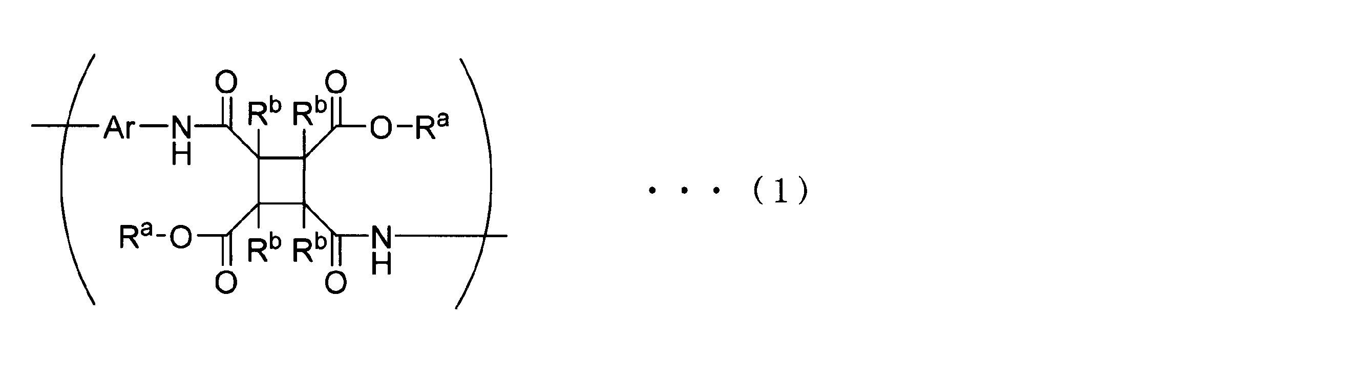
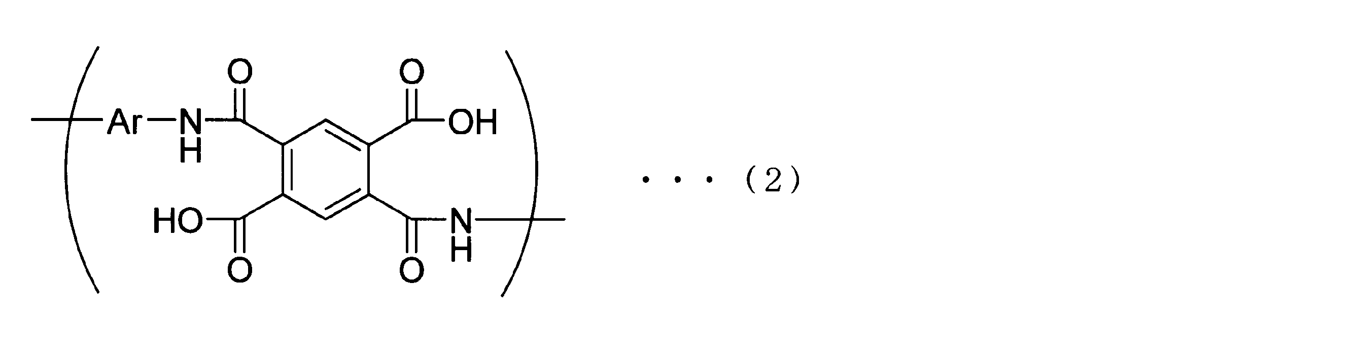
例えば配向膜材料に一定量(例えば、固形分全体において20質量%以上)のポリアミド酸エステルを含む場合、配向膜ワニスの主溶媒は、γ-ブチロラクトンを用いる。よって、規制部をポリアミド酸で形成すれば、配向膜ワニスのγ-ブチロラクトンと規制部の相溶性が悪い。よって、配向膜ワニスが規制部を乗り越えにくい。一方、配向膜材料において、ポリアミド酸が多量の場合(例えば、固形分全体において、80質量%以上)、配向膜ワニスの主溶媒は、N-メチル-2-ピロリドンを用いる。よって、規制部をポリアミド酸エステルで形成すれば、配向膜ワニスのN-メチル-2-ピロリドンと規制部の相溶性が悪い。よって、配向膜ワニスが規制部を乗り越えにくい。なお、最終的に各ポリアミド酸又はポリアミド酸エステルは、製造過程でポリイミドに変化する。
上述の記載を換言すれば、表示装置としては、配向膜と規制部の一方がポリアミド酸由来のポリイミドであり、他方がポリアミド酸エステル由来のポリイミドであると好ましい。なお、上述の記載は、配向膜ワニスの撥液現象の一例を述べただけである。よって、配向膜ワニスが規制部を乗り越えにくいのであれば、配向膜及び規制部は他の材料で形成されてもよい。
[(6)規制部-断面]
図5は、実施の形態1で、図4のC-C線に対応する、規制部DM1(特に下辺規制部DM11)のY方向とZ方向との断面(Y-Z面)での概略構成を示す。図5では、第1基板SB1の絶縁膜INS1の上面である第1面sf1上における、規制部DM1および配向膜AL1の端部を示す。第1面sf1は、配向膜AL1および規制部DM1の下地面であり、同じ高さ位置にある。
図5は、実施の形態1で、図4のC-C線に対応する、規制部DM1(特に下辺規制部DM11)のY方向とZ方向との断面(Y-Z面)での概略構成を示す。図5では、第1基板SB1の絶縁膜INS1の上面である第1面sf1上における、規制部DM1および配向膜AL1の端部を示す。第1面sf1は、配向膜AL1および規制部DM1の下地面であり、同じ高さ位置にある。
図5の規制部DM1の断面形状は、図示の通り、概略的に凹形状であり、Y方向の中心位置y0で低くなっており、内端部E1および外端部E2と対応する外側の位置y1,y2に近い位置で高くなっている。図5では、Z方向の配向膜AL1の厚さを厚さT2、規制部DM1の厚さを厚さT1で示す。配向膜AL1の厚さT2よりも規制部DM1の厚さT1の方が大きい(T2<T1)。言い換えると、規制部DM1の方が配向膜AL1よりも高い。実施の形態1では、特に、規制部DM1の厚さT1は、1000nm以下としている(T1≦1000nm)。好ましくは、厚さT1は150nm以上である。
図5の規制部DM1は、インクジェット方式を用いて形成されている。すなわち、インクジェット装置のヘッドのノズルから、方向Z2で、第1面sf1に対し、規制部材料の液滴が吐出されることで、第1基板SB1上に規制部材料が塗布される。その液滴が乾燥等によって固化されることで、規制部DM1が形成される。この際、公知のコーヒーステイン現象と同様の原理(中央部に対し外周部の溶質の濃度が高くなる等の原理)によって、この規制部DM1の凹形状が形成される。規制部DM2についてもこれと同様である。
規制部DM1の内端部E1では、配向膜AL1の端部がせき止められて、厚さT2の高さよりも上方の位置まで盛り上がっている。配向膜AL1の端部における、規制部DM1の内端部E1に接する部分では、跳ね返りのムラが生じる。このムラが生じる領域を、図5ではムラ領域501として示す。このムラ領域501は、非表示領域NAに含まれる。
なお、図5では特にある凸部42の位置での断面を示しており、配向膜AL1の端部の高さが、規制部DM1の内端部E1の高さ(厚さT1)以下となっている場合を示す。規制部DM1と配向膜AL1の端部との形状の関係は、図5の例に限らず可能である。配向膜AL1の端部の高さが、規制部DM1の内端部E1の高さ(厚さT1)よりも大きくなってもよい。
図6は、図5に対する変形例における規制部DM1および配向膜AL1の断面の形状の概略構成を示す。図6の構成例では、配向膜AL1の端部が、規制部DM1の内端部E1の高さ(厚さT1)を超えて盛り上がった形状となっている。図6では特にある凹部41の位置(例えば図4のD-D線)での断面を示す。この盛り上がった端部は、非表示領域NA内となるので、表示領域DAには影響しない。また、他の構成例では、配向膜AL1の端部が、規制部DM1の凹形状内部に入り込んでもよい。
図23は、変形例における規制部DM1および配向膜AL1の断面の形状の概略構成を示す。この規制部DM1の断面形状は、図示の通り、概略的に凸形状であり、Y方向の中心位置y0で高くなっており、外側の位置y1,y2で低くなっている。このような規制部DM1の形状でも、同様に、配向膜端部ムラ低減の効果が得られる。
[(7-1)規制部-変形例]
図7は、実施の形態1の変形例の液晶表示装置1で、規制部DM1の平面視の概略構成を示す。図7の規制部DM1は、図4の規制部DM1の内端部E1側の半分の構成に対応する。外端部E2は直線状となっている。この内端部E1の凹凸形状は、言い換えると、複数の半円の繰り返しによる形状である。
図7は、実施の形態1の変形例の液晶表示装置1で、規制部DM1の平面視の概略構成を示す。図7の規制部DM1は、図4の規制部DM1の内端部E1側の半分の構成に対応する。外端部E2は直線状となっている。この内端部E1の凹凸形状は、言い換えると、複数の半円の繰り返しによる形状である。
[(7-2)規制部-変形例]
図8は、他の変形例で、規制部DM1の平面視の概略構成を示す。図8の規制部DM1は、内端部E1において、波形状を有する。この内端部E1の凹凸形状では、凸部42は、中心線c1に対し、方向Y1に出る曲面を持ち、凹部41は反対に方向Y2に入り込む曲面を持つ。この波形状は、サイン波等の形状としてもよい。
図8は、他の変形例で、規制部DM1の平面視の概略構成を示す。図8の規制部DM1は、内端部E1において、波形状を有する。この内端部E1の凹凸形状では、凸部42は、中心線c1に対し、方向Y1に出る曲面を持ち、凹部41は反対に方向Y2に入り込む曲面を持つ。この波形状は、サイン波等の形状としてもよい。
[(7-3)規制部-変形例]
図9は、他の変形例で、規制部DM1の平面視の概略構成を示す。図9の規制部DM1の形状は、Y方向の2つの位置の中心線j1,j2に沿って、それぞれ、X方向に複数の円の連なりが配置されている。各位置の中心線j1,j2では、複数の円の各円は、所定の間隔pt2で円間に隙間を設けながら断続的に配置されている。2つの中心線j1,j2上の2列の円群を合わせた形状でみると、各円は、所定の間隔pt3で配置されている。この規制部DM1は、全体でみると、内端部E1に凹部41および凸部42が構成されている。
図9は、他の変形例で、規制部DM1の平面視の概略構成を示す。図9の規制部DM1の形状は、Y方向の2つの位置の中心線j1,j2に沿って、それぞれ、X方向に複数の円の連なりが配置されている。各位置の中心線j1,j2では、複数の円の各円は、所定の間隔pt2で円間に隙間を設けながら断続的に配置されている。2つの中心線j1,j2上の2列の円群を合わせた形状でみると、各円は、所定の間隔pt3で配置されている。この規制部DM1は、全体でみると、内端部E1に凹部41および凸部42が構成されている。
凹部41は、一方の内側寄りの中心線j1上におけるX方向で隣り合う2つの円と、それらの間にある他方の中心線j2上の円とで形成されている。凸部42は、中心線j2上の2つの円の間にある中心線j1上の1つの円の一部によって形成されている。幅H3は、一方の中心線j1上の円の列における幅(1つの円の最大の幅)を示す。他方の中心線j2上の円の列における幅も、幅H3と同じである。図9の構成例では各円のサイズが同じ場合を示すが、これに限らず可能である。図9の構成で、図4の場合と同様に、幅W1、幅W2をとることができる。幅W1は、図示の通りであり、一方の線上の円の内端と他方の線上の円の内端との距離に対応する。幅W2は、図示の通りであり、2つの列における2つの円が連続している部分における最大の幅となる。
この変形例の規制部DM1の形状も、特にインクジェット方式での形成が可能である。すなわち、インクジェット装置のヘッドから、2つの中心線j1,j2の位置でそれぞれ、規制部材料の液滴を吐出するように、ヘッド位置またはノズル位置等を制御すればよい。また、インクジェット装置で、走査中にヘッドのノズルから液滴を吐出する際の間隔や液滴の大きさ(圧力等)を制御すればよい。インクジェット装置による制御によって、規制部DMの凹凸形状の詳細形状が制御可能である。上記のような2列での液滴群の形成に限らず、3列以上での形成としてもよい。また、従来のインクジェット装置で、X方向に沿って複数の液滴を吐出する際に、Y方向での位置ズレが生じる場合には、その位置ズレの特性を利用して、このような規制部DMの凹凸形状を形成することができる。
[(7-4)規制部-変形例]
図10は、他の変形例で、規制部DM1の平面視の概略構成を示す。この図10の規制部DM1の形状は、中心線C1に沿ってY方向(方向Y1,Y2)に波状に蛇行または振動する形状である。この構成では内端部E1および外端部E2の両方に凹凸形状を有する。内端部E1には、凹部41、凸部42を有し、波の曲線による斜面を持つ。この構成でも幅W1および幅W2を同様にとることができる。この規制部DM1の形状は、例えば、製造時に製造装置によって規制部材料をX方向に沿って塗布する際に、Y方向の位置の蛇行や振動を制御することで、形成可能である。
図10は、他の変形例で、規制部DM1の平面視の概略構成を示す。この図10の規制部DM1の形状は、中心線C1に沿ってY方向(方向Y1,Y2)に波状に蛇行または振動する形状である。この構成では内端部E1および外端部E2の両方に凹凸形状を有する。内端部E1には、凹部41、凸部42を有し、波の曲線による斜面を持つ。この構成でも幅W1および幅W2を同様にとることができる。この規制部DM1の形状は、例えば、製造時に製造装置によって規制部材料をX方向に沿って塗布する際に、Y方向の位置の蛇行や振動を制御することで、形成可能である。
[(7-5)規制部-変形例]
図11は、他の変形例で、規制部DM1の平面視の概略構成を示す。この規制部DM1の形状は、内端部E1において、台形状の凹部41および凸部42を有する。この凹部41および凸部42の台形は、X方向に延在する短辺と、その短辺からY方向に対して斜めとなる斜辺とを有する。この構成でも幅W1および幅W2を同様にとることができる。外端部E2側でも内端部E1側と同様の形状としてもよい。
図11は、他の変形例で、規制部DM1の平面視の概略構成を示す。この規制部DM1の形状は、内端部E1において、台形状の凹部41および凸部42を有する。この凹部41および凸部42の台形は、X方向に延在する短辺と、その短辺からY方向に対して斜めとなる斜辺とを有する。この構成でも幅W1および幅W2を同様にとることができる。外端部E2側でも内端部E1側と同様の形状としてもよい。
[(7-6)規制部-変形例]
図12は、他の変形例で、規制部DM1の平面視の概略構成を示す。この規制部DM1の形状は、内端部E1において、三角形状の凹部41および凸部42を有する。この凹部41および凸部42の三角形は、Y方向に対して斜めとなる斜辺を有する。この構成でも幅W1および幅W2を同様にとることができる。外端部E2側でも内端部E1側と同様の形状としてもよい。上記のような各種の変形例の規制部でも、配向膜の広がりの規制および跳ね返りのムラ低減に関する相応の効果が得られる。
図12は、他の変形例で、規制部DM1の平面視の概略構成を示す。この規制部DM1の形状は、内端部E1において、三角形状の凹部41および凸部42を有する。この凹部41および凸部42の三角形は、Y方向に対して斜めとなる斜辺を有する。この構成でも幅W1および幅W2を同様にとることができる。外端部E2側でも内端部E1側と同様の形状としてもよい。上記のような各種の変形例の規制部でも、配向膜の広がりの規制および跳ね返りのムラ低減に関する相応の効果が得られる。
[比較例(1)]
図20は、実施の形態1に対する第1比較例の液晶表示装置における規制部201、および実施の形態1での第2規制部DMB(図3)について、実施の形態1の第1規制部DMAとの比較で、平面視の概略構成を示す。この規制部201(第2規制部DMB)は、一方向(例えばX方向)に所定の幅H1(H1=W2)で延在する直線状である。この規制部201(第2規制部DMB)の内端部E1は、第1幅である幅W1(特に幅W12とする)を考えた場合、実質的に0である(W1=W12≒0)。
図20は、実施の形態1に対する第1比較例の液晶表示装置における規制部201、および実施の形態1での第2規制部DMB(図3)について、実施の形態1の第1規制部DMAとの比較で、平面視の概略構成を示す。この規制部201(第2規制部DMB)は、一方向(例えばX方向)に所定の幅H1(H1=W2)で延在する直線状である。この規制部201(第2規制部DMB)の内端部E1は、第1幅である幅W1(特に幅W12とする)を考えた場合、実質的に0である(W1=W12≒0)。
実施の形態1における第1規制部DMAの内端部E1の凹凸形状は、所定の大きさ以上で幅W1(特に幅W11とする)を設ける。第1規制部DMAの内端部E1の第1幅(幅W11)は、規制部201(第2規制部DMB)の内端部E1の第1幅(幅W12)よりも大きい(W11>W12)。これにより、実施の形態1の第1規制部DMAでは、少なくとも規制部201(第2規制部DMB)の場合よりも、配向膜ワニスの跳ね返りのムラを低減する効果が得られる。
[比較例(2)]
図21は、実施の形態1に対する第2比較例の液晶表示装置における規制部202の平面視の概略構成を、実施の形態1の第1規制部DMAとの比較で示す。この規制部202の形状は、X方向に延在する中心線C1に沿って所定の幅で延在するジグザグ形状である。幅H4は、ジグザグの方向に垂直な方向での幅を示す。このジグザグ形状の側面部(内端部および外端部)は、三角波形状である。この規制部202における凹部241および凸部242を考える。また、この凹部241および凸部242における第1幅(幅W1、特に幅W13とする)および第2幅(幅W2、特に幅W23とする)を考える。規制部202では、この幅W1(W13)は幅W2(W23)よりも大きい(W1>W2)。一方、実施の形態1の規制部DM1では、この幅W1(W11)は幅W2以下である(W1≦W2)。
図21は、実施の形態1に対する第2比較例の液晶表示装置における規制部202の平面視の概略構成を、実施の形態1の第1規制部DMAとの比較で示す。この規制部202の形状は、X方向に延在する中心線C1に沿って所定の幅で延在するジグザグ形状である。幅H4は、ジグザグの方向に垂直な方向での幅を示す。このジグザグ形状の側面部(内端部および外端部)は、三角波形状である。この規制部202における凹部241および凸部242を考える。また、この凹部241および凸部242における第1幅(幅W1、特に幅W13とする)および第2幅(幅W2、特に幅W23とする)を考える。規制部202では、この幅W1(W13)は幅W2(W23)よりも大きい(W1>W2)。一方、実施の形態1の規制部DM1では、この幅W1(W11)は幅W2以下である(W1≦W2)。
また、この規制部202のジグザグ形状のX方向での凸部242の間隔を間隔pt4で示す。この規制部202における凹凸の形成の間隔pt4は、実施の形態1での規制部DM1の凹凸の間隔pt1よりも大きい(pt4>pt1)。言い換えると、実施の形態1での規制部DM1の凹凸形状は、このような規制部202のジグザグ形状よりも小さいスケールで形成されている。このような規制部202の場合、内端部側で、ジグザグ形状のうちの各々の斜面では、直線状である。このような規制部202の場合、規制部202の幅H1と、配向膜ワニスの跳ね返りのムラの幅とを含めた総合的な幅を考えた場合、その総合的な幅が大きく、非表示領域を低減する効果は得られない。
[(8)規制部-作用]
図13、図14を用いて、規制部DM1の凹凸形状の作用や効果についてより詳しく説明する。図13は、図20のような第1比較例の規制部201と、実施の形態1での規制部DM1(第1規制部DMA)の構成例とで対比して、平面視の概略構成を示す。図13の上側の(A)では、平らな第1面sf1上における、第1配向膜AL1の端部に対応する、配向膜ワニスの領域131と、直線状の規制部201とを示す。規制部201は、X方向に延在している。配向膜ワニスに対応する塗布液は、基本的に、方向Y2に対応する方向401で広がる。その配向膜ワニスは、方向402に跳ね返される。これにより、配向膜ワニスのムラ領域132が生じる。このムラ領域132では、X方向の各位置で、材料の跳ね返りの度合いが異なっており、厚さや形状にムラがある。ムラ領域132のY方向の幅を幅M1で示す。
図13、図14を用いて、規制部DM1の凹凸形状の作用や効果についてより詳しく説明する。図13は、図20のような第1比較例の規制部201と、実施の形態1での規制部DM1(第1規制部DMA)の構成例とで対比して、平面視の概略構成を示す。図13の上側の(A)では、平らな第1面sf1上における、第1配向膜AL1の端部に対応する、配向膜ワニスの領域131と、直線状の規制部201とを示す。規制部201は、X方向に延在している。配向膜ワニスに対応する塗布液は、基本的に、方向Y2に対応する方向401で広がる。その配向膜ワニスは、方向402に跳ね返される。これにより、配向膜ワニスのムラ領域132が生じる。このムラ領域132では、X方向の各位置で、材料の跳ね返りの度合いが異なっており、厚さや形状にムラがある。ムラ領域132のY方向の幅を幅M1で示す。
(A)に対応して、右側には、規制部201等の断面を示す。規制部201の幅H1と、ムラ領域132の幅M1とを総合した幅(H1+M1)を示す。ムラ領域132は、画素の光学的な特性の均一性を確保できないので、非表示領域NAに含まれる。これにより、その分、表示領域DAが小さくなり、額縁領域FAが大きくなる。
図13の下側の(B)には、同様に、平らな第1面sf1上における、第1配向膜AL1の端部に対応する、配向膜ワニスの領域133と、凹凸形状の規制部DM1とを示す。この規制部DM1の形状は、図4のモデル形状に基づいて、インクジェット方式での形成時に、Y方向で所定の範囲内での位置ズレがある場合の形状例を示す。配向膜ワニスに対応する塗布液は、基本的に、方向Y2に対応する方向401で広がる。その配向膜ワニスは、規制部DM1の内端部E1に当たって、反対の方向402に跳ね返される。これにより、配向膜ワニスのムラ領域134が生じる。ムラ領域134のY方向の幅を幅M2で示す。幅M2は、幅M1よりも小さくなっている(M2<M1)。
配向膜ワニスが内端部E1に当たって跳ね返される際、内端部E1の凹凸形状によって、X方向の各位置での材料の跳ね返りの差が小さくなるように緩和されている。配向膜ワニスは、凹部41および凸部42の曲面(斜面)に当たって、その曲面(斜面)に応じた方向に反射される。言い換えると、塗布液の波エネルギーは、内端部E1の凹凸形状によって、方向401および方向402とは異なる斜めの各方向に分散される。この結果、ムラ領域134の幅M2が、幅M1よりも小さくなる。なお、幅M2は、内端部E1の凹凸形状におけるY方向で最も内側に出た部分の位置から、ムラ領域133の最も内側の位置までの長さとしている。
(B)に対応して、右側には、規制部DM1等の断面を示す。規制部DM1の幅H1と、ムラ領域134の幅M2とを総合した幅(H1+M2)を示す。この総合的な幅(H1+M2)は、比較例の総合的な幅(H1+M1)よりも小さい。このように、実施の形態1では、規制部DM1の全体の幅H1を規制部201の全体の幅H1と同じとした場合でも、ムラ領域134の幅M2をより小さく抑えることができる。実施の形態1では、ムラ領域134の幅M2を含む総合的な幅(H1+M2)を小さく抑えることができる。よって、その分、非表示領域NA(額縁領域FA)を小さく、表示領域DAを大きくすることができる。
図14は、規制部DM1の内端部E1の凹凸形状に対する、配向膜ワニスの跳ね返りに関して模式的に示す。(A)は、規制部DM1の形状の第1例の場合を示し、図4のモデル形状に基づいている。(B)は、規制部DM1の形状の第2例の場合を示し、図9の変形例の形状に基づいている。それぞれ、1つのリング状の円形は、インクジェット方式の1つの液滴に対応している。(A)で、配向膜ワニスの分子は、各矢印で示す方向401(方向Y2)で、内端部E1の凸部42の曲面(斜面)42aに当たり、その曲面42aの傾きの方向に応じた方向に反射される。分子の当たった位置に応じて異なる各方向に分子が反射される。反射された分子は、さらに曲面42aに当たった場合には同様に反射される。ある分子は、凹部41の奥に入り込むように反射され、ある分子は、凹部41から方向Y1へ戻るように反射される。(B)で、同様に、配向膜ワニスの分子は、各矢印で示す方向401(方向Y2)で、内端部E1の凸部42の曲面(斜面)42aや凹部41の曲面(斜面)41aに当たり、その曲面42aや曲面41aの傾きの方向に応じた方向に反射される。このように、配向膜ワニスの分子の跳ね返りの方向が分散されるので、全体でみるとムラ領域134の幅M2が小さくなる。
[(9)規制部形成方法]
図3や図15を用いて、実施の形態1の液晶表示装置1での規制部DM(DM1,DM2)の形成方法について説明する。実施の形態1では、インクジェット方式を用いて、第1基板SB1の第1面sf1上に図4のような凹凸形状の規制部DM1を形成する。規制部DM1や配向膜AL1の形成方法の概要は以下である。
図3や図15を用いて、実施の形態1の液晶表示装置1での規制部DM(DM1,DM2)の形成方法について説明する。実施の形態1では、インクジェット方式を用いて、第1基板SB1の第1面sf1上に図4のような凹凸形状の規制部DM1を形成する。規制部DM1や配向膜AL1の形成方法の概要は以下である。
(1)予め、第1基板SB1の絶縁膜INS1(図2)までが形成されているとする。(2)製造装置として、インクジェット装置は、第1基板SB1の絶縁膜INS1の第1面sf1上に、規制部材料(ワニス)の液滴の吐出によって、規制部材料を塗布する。(3)製造装置は、第1基板SB1上の規制部材料を、乾燥等によって固化する。これにより、規制部DM1が形成される。
(4)次に、製造装置は、第1基板SB1の絶縁膜INS1の第1面sf1上において、規制部DM1よりも内側の領域に、第1配向膜AL1の配向膜ワニスを塗布する。この工程では例えばインクジェット装置が用いられる。インクジェット装置は、その領域に、配向膜ワニスの液滴の吐出によって、配向膜ワニスを塗布する。その際、規制部DM1によって、前述のように、配向膜ワニスの無用な広がりが規制され、端部のムラが抑制される。
(5)製造装置は、第1基板SBI上の第1配向膜AL1の配向膜ワニスを、乾燥等によって固化する。(6)製造装置は、第1基板SB1上の規制部材料、および、第1基板SBI上の第1配向膜AL1の配向膜ワニスを、焼成等によって反応させる。(7)製造装置は、例えば光配向方式を用いて配向膜AL1を配向処理する。これにより、配向膜AL1が形成される。第2基板SB2側の規制部DM2および配向膜AL2についても上記と同様に形成可能である。
さらに、規制部DM1の形成方法の詳細は以下である。この形成方法では、インクジェット方式の特性を利用して、規制部DM1の凹凸形状を容易かつ効率的に形成する。この形成方法では、特に、インクジェット方式のヘッド用のレールが伸びる方向である主走査方向と、それに交差する副走査方向との精度の違いを利用して、2種類の規制部を形成する。主走査方向及び副走査方向の概要は、例えば米国公開公報2014/0062076の図3に開示されている。
前述の図3の前面構成において、実線矢印で示す方向DIR1は、インクジェット方式のヘッドの主走査方向を示し、破線矢印で示す方向DIR2は、そのヘッドの副走査方向を示す。この形成方法では、方向DIR1はY方向と対応させており、方向DIR2はX方向と対応させている。インクジェット装置は、材料の塗布の際、線順次に走査を行う。インクジェット装置は、ヘッドをインクジェット装置のレールに沿って、方向DIR1で線状に主走査をする。そして、インクジェット装置は、1本の線の走査が終わる毎に、ヘッドを方向DIR2に移動させるように副走査をする。インクジェット装置は、ヘッドの主走査において、ヘッドのノズルから、材料の液滴を吐出する。インクジェット装置は、走査において、規制部DM1を形成する領域と形成しない領域とで、規制部材料の吐出の有無等を制御する。
図3で、第3外周領域L3や第4外周領域L4のように、第2規制部DMBを形成する領域では、方向DIR1に沿ってヘッドから規制部材料の液滴が連続的に吐出される。これにより、直線状の第2規制部DMBが形成できる。また、第1外周領域L1や第2外周領域L2のように、第1規制部DMAを形成する領域では、方向DIR1に沿って、その領域上に来た時に、ヘッドから規制部材料の液滴が吐出される。第1規制部DMAの領域はX方向に延在しているので、インクジェット装置は、方向DIR2の副走査によって対応する。
方向DIR1の主走査では、キャリッジレールに沿ってヘッドの連続的な移動が可能であるが、方向DIR2の副走査では、ヘッド又は被吐出媒体の機械的な移動が必要であるため、方向DIR1の主走査よりも移動の精度が劣る。すなわち、副走査の方向DIR2では、材料の形成(吐出)の位置や間隔の精度が、主走査の方向DIR1よりも劣る。そこで、この形成方法では、第1規制部DMAの凹凸形状の領域および方向を、ヘッドの副走査の方向DIR2と対応させている。副走査の方向DIR2では、ヘッドの機械的な駆動による移動が行われる。これに対応して、第1規制部DMAを形成する領域におけるX方向の液滴の吐出の位置や間隔が決まる。この間隔は、第2規制部DMBの領域におけるY方向の液滴の吐出の間隔よりも広くなる。これにより、第1規制部DMAにおける凹凸形状が形成できる。
なお、公知のインクジェット装置では、走査時、キャリッジレールに沿ってヘッド(インクジェットヘッド)を移動させながら、ヘッドのノズルから下方に液滴が吐出される。ヘッドにおける、液滴の吐出間隔やノズルの配置位置等については各種の構成が可能であり、それらを利用することでも、規制部DMの凹凸形状を形成可能である。
図15は、さらに、製造方法の一例についての説明図を示す。図15では、マザー基板150上において、複数の液晶表示装置本体(または第1基板SB1等)がまとめて形成され、カットによって個々の液晶表示装置本体が構成される場合について、平面視の概略構成を示す。番号#1~#3等は、個々の液晶表示装置本体の部分を示す。個々の液晶表示装置本体は、第1基板SB1上の規制部DM1を含む。
規制部DM1の形成時、方向DIR1(Y方向と対応する)では、上記のようにインクジェット方式の主走査が行われ、方向DIR2(X方向と対応する)では、副走査が行われる。これにより、複数の液晶表示装置本体に関して、X方向に延在する第1規制部DMA、およびY方向に延在する第2規制部DMBがまとめて形成される。形成後、マザー基板150からのカットによって、個々の液晶表示装置本体が取り出される。個々の液晶表示装置本体では、外周における4つの辺が形成される。
個々の液晶表示装置本体(液晶表示装置1)の一部として、規制部DM1の角部151について、拡大して下側に示す。この拡大図で、第1規制部DMAと第2規制部DMBとの2種類の規制部DMにおける、複数の液滴の円の配置の密度や間隔等の違いについて、模式的に示している。例えば右辺部(第4外周領域L4)に対応する第2規制部DMB(右辺規制部DM14)では、主走査の方向DIR1において、複数の液滴の円が、第1規制部DMAよりも、密に配置されている。例えば下辺部(第1外周領域L1)に対応する第1規制部DMA(下辺規制部DM11)では、副走査の方向DIR2において、複数の液滴の円が、第2規制部DMAよりも、疎に配置されている。これにより、第1規制部DMAでは内端部E1が凹凸形状となり、第2規制部DMBでは内端部E1が概略直線状となっている。
なお、この拡大図の構成イメージに限らず、ヘッドからの液滴の吐出の数や間隔や大きさ(圧力等)、ヘッドやノズルが走査する位置や数等について制御することで、各種の構成が可能である。他の形成方法の例としては、第1規制部DMAについて、ヘッドの主走査の方向DIR1を適用する。その場合に、インクジェット装置は、主走査時、ヘッドからの規制部材料の液滴の吐出の間隔を制御する。これにより、規制部DM1の凹凸形状を形成可能である。
[(10)規制部-実装構成例]
図16は、実施の形態1の液晶表示装置1で、規制部DMを含む主要部の実装構成例について、断面(Y-Z面)の概略構成を示す。図16の実装構成例は、インクジェット方式で規制部DMを形成する場合に対応している。第1基板SB1において、Z方向(方向Z1)でトランジスタTR上の絶縁膜INS11を有する。絶縁膜INS11は、トランジスタTRの端子電極ES(例えばソース端子電極)を覆っている。絶縁膜INS11は、Y方向で、表示領域DA、非表示領域NA、および延長領域EAにわたって形成されている。
図16は、実施の形態1の液晶表示装置1で、規制部DMを含む主要部の実装構成例について、断面(Y-Z面)の概略構成を示す。図16の実装構成例は、インクジェット方式で規制部DMを形成する場合に対応している。第1基板SB1において、Z方向(方向Z1)でトランジスタTR上の絶縁膜INS11を有する。絶縁膜INS11は、トランジスタTRの端子電極ES(例えばソース端子電極)を覆っている。絶縁膜INS11は、Y方向で、表示領域DA、非表示領域NA、および延長領域EAにわたって形成されている。
絶縁膜INS11上には、平坦化膜PF1を有する。平坦化膜PF1は、絶縁膜INS12で構成されている。平坦化膜PF1は、Y方向で、表示領域DAおよび非表示領域NAにわたって形成されている。平坦化膜PF1上には、例えば共通電極ECが形成されている。
平坦化膜PF1上には、共通電極ECを覆うように、平坦化膜PF2が形成されている。平坦化膜PF2は、絶縁膜INS13で構成されている。平坦化膜PF2(絶縁膜INS13)は、Y方向で、表示領域DA、非表示領域NA、および延長領域EAにわたって形成されている。平坦化膜PF2上には、例えば画素電極EPが形成されている。第1基板SB1の延長領域EAでは、平坦化膜PF1よりも外側に長く延在するように、平坦化膜PF2が形成されている。延長領域EAにおける絶縁膜INS11上の絶縁膜INS13において、一部の領域には、露出する端子部EEが形成されている。この端子部EEは、前述の回路部CC(図2)の一部、あるいは第1駆動回路部CD1(図3)の一部を構成している。
各画素の画素領域PAでは、第1基板SB1側に形成されている第1電極EL1として、共通電極ECおよび画素電極EPを有する。一般的な液晶表示装置では、少なくとも共通電極ECまたは画素電極EPの一方を有する。
この構成例では、第1面sf1は、表示領域DA等における絶縁膜INS13(平坦化膜PF2)の上面が対応する。第1面sf1である絶縁膜INS13の平らな上面上には、Y方向に、配向膜AL1、規制部DM1、封止部SL、等が形成されている。配向膜AL1は、画素電極EPを覆うようにして形成されている。
また、非表示領域NAを狭くするため、平面視で規制部DM1と重畳する位置に、映像信号線WR1と映像信号線WR2が形成されている。映像信号線WR1,WR2は、それぞれ複数本の配線で構成される。映像信号線WR1は絶縁膜で覆われており、その絶縁膜上に映像信号線WR2が配置されており、映像信号線WR2は絶縁膜INS1で覆われている。また、映像信号線WR1,WR2から出る電界を遮蔽するシールド電極SEも、規制部DM1と重畳している。シールド電極SEは、平坦化膜PF1上の共通電極ECと同一の層に形成されており、規制部DM1の形成に影響を与えない。シールド電極SEは、例えば規制部DM1のY方向の幅と同じ幅で形成され、平坦化膜PF2で覆われている。
第2基板SB2側には、方向Z2において、遮光膜BM、カラーフィルタCF、絶縁膜INS2等が形成されている。絶縁膜INS2の第2面sf2上には、Y方向で、第2配向膜AL2、封止部SL、等が形成されている。
本構成例では、Y方向における規制部DM1(および規制部DM2)の領域において、封止部SLとの関係では、重畳領域を持たず、すべてが非重畳領域r2となっている。非重畳領域r2は、平面視した場合に、規制部DMの領域のうち、封止部SLと重ならない領域である。
また、この構成例では、配向膜AL1、規制部DM1等を、インクジェット方式での塗布によって形成可能である。そのため、後述のパターニング方式に比べて、工程数が少なく効率的で低コストに形成が可能である。なお、封止部SLの材料は、ディスペンサーを用いて塗布をされる。
[(11-1)封止部]
図2や図16のように、実施の形態1では、規制部DM(DM1,DM2)は、封止部SLよりも内側に形成されており、封止部SLとの関係で非重畳領域r2を有する。この構成は、封止部SLの接着性能を優先する観点を考慮して選択されている。詳しくは、この構成は、封止部SL、絶縁膜INS1,INS2、配向膜AL1,AL2、規制部DM(DM1,DM2)等の要素の接着を考慮して選択されている。この構成では、封止部SLのZ方向の端部と、規制部DM以外の、絶縁膜(例えば絶縁膜INS1,INS2)の一部とが接着されている。材料や形状や形成方法等にも依存するが、非重畳領域r2が多く重畳領域が少ない構成の方が、接着性能をより高くできる。すなわち、この構成では、封止部SLによる第1基板SB1と第2基板SB2との間の接着をより強くすることができ、剥がれ等を防止できる。
図2や図16のように、実施の形態1では、規制部DM(DM1,DM2)は、封止部SLよりも内側に形成されており、封止部SLとの関係で非重畳領域r2を有する。この構成は、封止部SLの接着性能を優先する観点を考慮して選択されている。詳しくは、この構成は、封止部SL、絶縁膜INS1,INS2、配向膜AL1,AL2、規制部DM(DM1,DM2)等の要素の接着を考慮して選択されている。この構成では、封止部SLのZ方向の端部と、規制部DM以外の、絶縁膜(例えば絶縁膜INS1,INS2)の一部とが接着されている。材料や形状や形成方法等にも依存するが、非重畳領域r2が多く重畳領域が少ない構成の方が、接着性能をより高くできる。すなわち、この構成では、封止部SLによる第1基板SB1と第2基板SB2との間の接着をより強くすることができ、剥がれ等を防止できる。
なお、第2基板SB2側の規制部DM2に関しては、第1基板SB1側の規制部DM1と同様の構成としたが、これに限らず可能である。変形例としては、規制部DM2と規制部DM1とが異なる構成、例えばY方向の形成の位置が異なる構成としてもよい。また、変形例としては、規制部DM1のみを設ける構成や、規制部DM2のみを設ける構成も可能である。
[(11-2)封止部-変形例]
図17は、実施の形態1の変形例の液晶表示装置1で、封止部SLに関する断面(Y-Z面)の概略構成を示す。この構成では、Y方向で、封止部SLの外側に、規制部DM(DM1,DM2)が形成されている。配向膜AL1,AL2は、それぞれ、規制部DM1,DM2の内端部E1まで形成されている。封止部SLの方向Z2の端部は、絶縁膜INS1上の第1配向膜AL1に配置されている。封止部SLの方向Z1の端部は、絶縁膜INS2上の第2配向膜AL2に配置されている。この構成でも、規制部DMは、封止部SLとの関係では、すべての領域を非重畳領域r2としている。これにより、封止部SLの接着性能が確保されている。
図17は、実施の形態1の変形例の液晶表示装置1で、封止部SLに関する断面(Y-Z面)の概略構成を示す。この構成では、Y方向で、封止部SLの外側に、規制部DM(DM1,DM2)が形成されている。配向膜AL1,AL2は、それぞれ、規制部DM1,DM2の内端部E1まで形成されている。封止部SLの方向Z2の端部は、絶縁膜INS1上の第1配向膜AL1に配置されている。封止部SLの方向Z1の端部は、絶縁膜INS2上の第2配向膜AL2に配置されている。この構成でも、規制部DMは、封止部SLとの関係では、すべての領域を非重畳領域r2としている。これにより、封止部SLの接着性能が確保されている。
[(11-3)封止部-変形例]
図18は、他の変形例の液晶表示装置1で、封止部SLに関する断面(Y-Z面)の概略構成を示す。この構成では、Y方向で、封止部SLの内側に、一部の領域(重畳領域r1)で重畳するようにして、規制部DM1および規制部DM2が形成されている。この規制部DM1,DM2は、内端部E1側に非重畳領域r2を、外端部E2側に重畳領域r1を有する。この構成では、封止部SLと規制部DMとが一部の領域(重畳領域r1)で重なって配置されている。これにより、Y方向で、全体的に、規制部DMおよび封止部SLを含む要素を配置するための幅が短縮されている。そのため、非表示領域NAの幅をより短くし、額縁領域FA等をより狭くすることができる。すなわち、この構成は、封止部SLの接着性能よりも、狭額縁構成を優先する観点を考慮して選択されている。この構成では、封止部SLのうちの規制部DMとは重なっていない領域によって、封止部SLの接着性能が確保されている。なお、封止部SLの接着性能を十分に確保したい場合は、図17及び図16のような構成例を採用すると好ましい。
図18は、他の変形例の液晶表示装置1で、封止部SLに関する断面(Y-Z面)の概略構成を示す。この構成では、Y方向で、封止部SLの内側に、一部の領域(重畳領域r1)で重畳するようにして、規制部DM1および規制部DM2が形成されている。この規制部DM1,DM2は、内端部E1側に非重畳領域r2を、外端部E2側に重畳領域r1を有する。この構成では、封止部SLと規制部DMとが一部の領域(重畳領域r1)で重なって配置されている。これにより、Y方向で、全体的に、規制部DMおよび封止部SLを含む要素を配置するための幅が短縮されている。そのため、非表示領域NAの幅をより短くし、額縁領域FA等をより狭くすることができる。すなわち、この構成は、封止部SLの接着性能よりも、狭額縁構成を優先する観点を考慮して選択されている。この構成では、封止部SLのうちの規制部DMとは重なっていない領域によって、封止部SLの接着性能が確保されている。なお、封止部SLの接着性能を十分に確保したい場合は、図17及び図16のような構成例を採用すると好ましい。
[(11-4)封止部-変形例]
図19は、他の変形例の液晶表示装置1で、封止部SLに関する断面(Y-Z面)の概略構成を示す。この構成では、Y方向で、封止部SLの外側に、一部の領域(重畳領域r1)で重畳するようにして、規制部DM1および規制部DM2が形成されている。この規制部DM1,DM2は、外端部E2側に非重畳領域r2を、内端部E1側に重畳領域r1を有する。この構成も狭額縁構成を優先する観点で選択されており、同様の効果が得られる。この構成では、封止部SLのZ方向の端部は、配向膜AL1,AL2と接着されている。この封止部SLの材料等は、配向膜ワニスとの接着性能を考慮して選択される。
図19は、他の変形例の液晶表示装置1で、封止部SLに関する断面(Y-Z面)の概略構成を示す。この構成では、Y方向で、封止部SLの外側に、一部の領域(重畳領域r1)で重畳するようにして、規制部DM1および規制部DM2が形成されている。この規制部DM1,DM2は、外端部E2側に非重畳領域r2を、内端部E1側に重畳領域r1を有する。この構成も狭額縁構成を優先する観点で選択されており、同様の効果が得られる。この構成では、封止部SLのZ方向の端部は、配向膜AL1,AL2と接着されている。この封止部SLの材料等は、配向膜ワニスとの接着性能を考慮して選択される。
[効果等(1)]
上記のように、実施の形態1の液晶表示装置1によれば、規制部DMによって、配向膜(配向膜AL1,AL2)の端部形状のムラを改善でき、装置小型化や高密度実装に寄与できる。規制部DMによって、配向膜の端部のムラ領域を低減でき、ムラ領域および規制部を含む領域の幅を抑えることができる。よって、装置の前面の面積における、例えば表示領域DAと非表示領域NA(または額縁領域FAや回路領域CA等)との比率において、表示領域DAを大きくし非表示領域NAを小さくすることができる。すなわち、実施の形態1によれば、狭額縁構成等を実現できる。実施の形態1では、インクジェット方式を用いて規制部DM等を形成できるので、少ない工程数で、低コストおよび短時間で製造可能である。
上記のように、実施の形態1の液晶表示装置1によれば、規制部DMによって、配向膜(配向膜AL1,AL2)の端部形状のムラを改善でき、装置小型化や高密度実装に寄与できる。規制部DMによって、配向膜の端部のムラ領域を低減でき、ムラ領域および規制部を含む領域の幅を抑えることができる。よって、装置の前面の面積における、例えば表示領域DAと非表示領域NA(または額縁領域FAや回路領域CA等)との比率において、表示領域DAを大きくし非表示領域NAを小さくすることができる。すなわち、実施の形態1によれば、狭額縁構成等を実現できる。実施の形態1では、インクジェット方式を用いて規制部DM等を形成できるので、少ない工程数で、低コストおよび短時間で製造可能である。
(実施の形態2)
図24、図25を用いて、本発明の実施の形態2の液晶表示装置について説明する。実施の形態2では、規制部形成方法としてパターニング方式を用いる場合を示す。以下では、実施の形態2における実施の形態1とは異なる構成部分を説明する。
図24、図25を用いて、本発明の実施の形態2の液晶表示装置について説明する。実施の形態2では、規制部形成方法としてパターニング方式を用いる場合を示す。以下では、実施の形態2における実施の形態1とは異なる構成部分を説明する。
[規制部-実装構成例]
図24は、実施の形態2の液晶表示装置1で、規制部DMを含む実装構成例の主要部の断面(Y-Z面)の概略構成を示す。図24の構成は、インクジェット方式ではなく、マスクやエッチング等を用いた一般的なパターニング方式によって規制部DMを形成する場合の実装構成例を示す。パターニング方式では、製造装置としてエッチング装置等を用いる。
図24は、実施の形態2の液晶表示装置1で、規制部DMを含む実装構成例の主要部の断面(Y-Z面)の概略構成を示す。図24の構成は、インクジェット方式ではなく、マスクやエッチング等を用いた一般的なパターニング方式によって規制部DMを形成する場合の実装構成例を示す。パターニング方式では、製造装置としてエッチング装置等を用いる。
図24の断面の構成では、トランジスタTR上に絶縁膜INS21を有する。絶縁膜INS21は、表示領域DA、非表示領域NA、延長領域EAにわたって形成されている。下地となる絶縁膜INS21上において、Z方向で下側から上側へ順に、2層の絶縁膜として、絶縁膜INS22および絶縁膜INS23を有する。絶縁膜INS21上には、絶縁膜INS22を有する。絶縁膜INS22は、平坦化膜であり、特に有機絶縁膜で構成されている。絶縁膜INS22は、パターニングによって、表示領域DA、非表示領域NA、および延長領域EAのうちの一部(第2基板SB2の端から外側に位置Yaまでの領域)にわたって形成されている。絶縁膜INS22上には、パターニングによって、絶縁膜INS23が形成されている。絶縁膜INS23は、特に有機絶縁膜で構成されている。絶縁膜INS23は、表示領域DA、非表示領域NA、延長領域EAにわたって形成されている。
例えば、公知のFFS(Fringe-Field Switching)やIPS(In-Plane Switching)等の液晶方式(いわゆる横電界モード)では、この構成のように、下地の絶縁膜INS21と、第1電極EL1である例えば画素電極EPとの間に、これらの2層の絶縁膜(絶縁膜INS22,INS23)を有する。実施の形態2での規制部形成方法では、この構成に基づいて、2層の絶縁膜のパターニング加工によって、規制部DM1が形成されている。絶縁膜INS21の上面を第1面sf1とする。その第1面sf1上で、2層の絶縁膜(絶縁膜INS22,INS23)のパターニング加工によって、規制部DM1が形成されている。つまり、規制部DM1は、絶縁膜INS22および絶縁膜INS23の側面で形成されている。
また、絶縁膜INS22,INS23のパターニング加工によって、溝部GR、端子部EE等が形成されている。規制部DMの内端部E1側には、溝部GRが形成されている。溝部GRは、絶縁膜INS23の上面の高さ位置よりも下側に凹んでいる部分である。溝部GRは、内端部E1に合わせて、X方向に沿って延在している。規制部DM1の内端部E1の形成のために、溝部GRが必要である。図24では溝部GRのY方向の幅を幅WGで示す。溝部GRの深さは、絶縁膜INS22の厚さt1と絶縁膜INS23の厚さt2とを加えた厚さ(t1+t2)と対応している。
配向膜AL1は、画素電極EP(第1電極EL1)を覆うようにして、絶縁膜INS23上に形成されている。配向膜AL1の端部は、絶縁膜INS23の上面から溝部GR内の絶縁膜INS21の面に落ち込み、規制部DMの内端部E1でせき止められる。
なお、本構成例では、要素間の高さ関係として以下である。絶縁膜INS21の第1面sf1を基準とする。絶縁膜INS22の厚さを厚さt1、絶縁膜INS23の厚さを厚さt2、配向膜AL1の厚さを厚さt3とする。規制部DM1の高さ(厚さ)を高さh1、配向膜AL1の高さを高さh2とする。また、溝部GRにおける配向膜AL1の高さを高さh3とする。高さh1は、2層の絶縁膜の厚さの合計値(t1+t2)である。高さh2は、その合計に厚さt3を加えた合計値(t1+t2+t3)である。
絶縁膜INS22,INS23のパターニング加工であるため、配向膜AL1の下地面(面sf3)の高さ位置と、規制部DM1の上面(面sf4)の高さ位置とが同じとなる。よって、高さh2は、高さh1よりも大きい(h2>h1)。また、規制部DM1として機能するために、高さh3は、高さh1よりも小さいとされる(h3<h1)。まとめると、h2>h1>h3である。
また、この構成例では、溝部GRは、特に、Y方向で封止部SLの付近の位置に形成されており、平面視で溝部GRの領域が封止部SLの領域内に重畳している。封止部SLのZ方向の下側の端部の一部は、溝部GR内に入り込むようにして形成されている。これにより、この構成では、非表示領域NAの短縮と共に、封止部SLの接着性能を強めている。
この構成例では、Y方向での規制部DM1の領域は、内端部E1側の一部の領域が、封止部SLと重畳する重畳領域r1となっており、他の外端部E2側の領域が、非重畳領域r2となっている。重畳領域r1では、規制部DM1の上面(面sf4)の絶縁膜INS23と封止部SLの端部とが直接的に接触している。溝部GRでは、配向膜AL1と封止部SLの端部とが接触している。
この構成例では、規制部DM1、封止部SL、および溝部GRを含む領域が、非表示領域NAとなる。なお、第2基板SB2側の配向膜AL2についても、上記と同様に、パターニング方式によって規制部DM2が形成されてもよい。
また、この構成例でも、非表示領域NAにおいて、映像信号線WR1,WR2、およびシールド電極SEが形成されている。この映像信号線WR1,WR2、およびシールド電極SEは、封止部SLおよび溝部GRよりも内側の位置に形成されている。このシールド電極SEは、絶縁膜INS22上の共通電極ECと同一の層に形成され、絶縁膜INS23で覆われている。なお、これに限らず、シールド電極SEが溝部GR内に出て配向膜AL1等と接触するように形成されてもよい。
[溝部構成]
図25は、実施の形態2で、図24の溝部GRおよび規制部DM1の構成に関して、平面視の概略構成を示す。図25では、配向膜AL1の主要な領域251と、溝部GRの領域252と、規制部DM1とを示す。領域251は、図24の高さh2の領域に対応する。領域252は、図24の高さh3の領域に対応する。図25の規制部DM1は、図7と同様に内端部E1側で凹凸形状である場合を示すが、これに限らず各種の形状が可能である。
図25は、実施の形態2で、図24の溝部GRおよび規制部DM1の構成に関して、平面視の概略構成を示す。図25では、配向膜AL1の主要な領域251と、溝部GRの領域252と、規制部DM1とを示す。領域251は、図24の高さh2の領域に対応する。領域252は、図24の高さh3の領域に対応する。図25の規制部DM1は、図7と同様に内端部E1側で凹凸形状である場合を示すが、これに限らず各種の形状が可能である。
溝部GR内で、配向膜AL1(配向膜ワニス)の端部は、方向401で、規制部DM1の内端部E1の凹凸形状に当たって方向402で跳ね返される。その際、実施の形態1での作用と同様に、跳ね返りのムラが低減される。図25では跳ね返りのムラ領域253とそのムラ領域253の幅M3を示す。実施の形態2では、ムラ領域253の幅M3と規制部DM1の幅H1とを合わせた総合的な幅(H1+M3)を低減できる。
実施の形態2で、規制部DM1の凹凸の幅W1は、実施の形態1と同様に、W1≦100μmとされる。また、例えば、溝部GRの幅WGは200μm以下とされる(WG≦200μm)。溝部GRの幅WGは、例えば凹凸の形成の間隔pt5に対し、2倍程度とされる(WG≒pt5×2)。
[効果等(2)]
上記のように、実施の形態2の液晶表示装置1によれば、実施の形態1と同様に、規制部DMによって、配向膜(配向膜AL1)の端部形状のムラを改善でき、装置の小型化や高密度実装に寄与できる。すなわち、実施の形態2によれば、狭額縁構成等を実現できる。実施の形態2では、パターニング方式を用いるので、形成時に、マスク、エッチング等の複数の工程が必要であるが、パターニング加工によって規制部DMの凹凸形状を詳細に制御可能である。
上記のように、実施の形態2の液晶表示装置1によれば、実施の形態1と同様に、規制部DMによって、配向膜(配向膜AL1)の端部形状のムラを改善でき、装置の小型化や高密度実装に寄与できる。すなわち、実施の形態2によれば、狭額縁構成等を実現できる。実施の形態2では、パターニング方式を用いるので、形成時に、マスク、エッチング等の複数の工程が必要であるが、パターニング加工によって規制部DMの凹凸形状を詳細に制御可能である。
(実施の形態3)
図26~図39を用いて、本発明の実施の形態3の液晶表示装置について説明する。以下では、実施の形態3における実施の形態1,2とは異なる構成部分を説明する。実施の形態3の液晶表示装置は、他の形状を持つ規制部を有する。
図26~図39を用いて、本発明の実施の形態3の液晶表示装置について説明する。以下では、実施の形態3における実施の形態1,2とは異なる構成部分を説明する。実施の形態3の液晶表示装置は、他の形状を持つ規制部を有する。
[規制部-概要]
実施の形態3の液晶表示装置は、例えば図3と同様に、第1規制部DMAである下辺規制部DM11および上辺規制部DM12において、例えば図26のように第1基板SB1側および第2基板SB2側に、特有の形状の規制部DM(DM1,DM2)を備える。この特有の形状の規制部DMは、後述の図27のように、隙間を持つ複数の領域を有する。
実施の形態3の液晶表示装置は、例えば図3と同様に、第1規制部DMAである下辺規制部DM11および上辺規制部DM12において、例えば図26のように第1基板SB1側および第2基板SB2側に、特有の形状の規制部DM(DM1,DM2)を備える。この特有の形状の規制部DMは、後述の図27のように、隙間を持つ複数の領域を有する。
図26は、実施の形態3の液晶表示装置1で、下辺規制部DM11の規制部DM(DM1,DM2)、配向膜AL(AL1,AL2)、および封止部SL等に関する断面(Y-Z面)の構成例を示す。図27は、図26の特に第1基板SB1側の規制部DM11に関して、特有の形状の規制部の構成例を示す。図27の(A)は第1構成例の規制部DM31の概略構成を示し、(B)は第2構成例の規制部DM32の概略構成を示す。実施の形態3で、第1規制部DMAは、図27のような規制部DM31または規制部DM32によって構成される。図28は、第1構成例の規制部DM31等の平面視の詳細構成を示す。図29は、第2構成例の規制部DM32等の平面視の詳細構成を示す。図30は、第1構成例の規制部DM31に関する第1変形例の規制部DM33の平面視の詳細構成を示す。図31は、第2構成例の規制部DM32に関する第2変形例の規制部DM34の平面視の詳細構成を示す。図32~図38は、実施の形態3での各種の変形例の規制部の構成を示す。図39は、実施の形態3に対する比較例の規制部DM30等の構成を示す。
[規制部および封止部-断面]
図26の断面で、この構成例では、Y方向で、非表示領域NAにおいて、配向膜AL(AL1,AL2)の端部の外側に、規制部DM(DM1,DM2)の領域261、および封止部SLの領域260を有する。Y方向で、封止部SLの領域260において、規制部DMの領域261がすべて重畳して含まれるように配置されている。Y方向で、規制部DMの領域261の内端部E1および外端部E2の両側には、規制部DMが重畳していない封止部SLの領域がある。この構成例では、規制部DMと封止部SLとが重畳して配置されている。よって、規制部DMおよび封止部SLのために必要な領域の全体的な幅が少なく、非表示領域NAの幅を少なくできるので、狭額縁構成に有利である。実施の形態3における規制部DMおよび封止部SLに関する断面構成は、この構成例に限らず、実施の形態1等で説明した各種の構成例が同様に適用可能である。
図26の断面で、この構成例では、Y方向で、非表示領域NAにおいて、配向膜AL(AL1,AL2)の端部の外側に、規制部DM(DM1,DM2)の領域261、および封止部SLの領域260を有する。Y方向で、封止部SLの領域260において、規制部DMの領域261がすべて重畳して含まれるように配置されている。Y方向で、規制部DMの領域261の内端部E1および外端部E2の両側には、規制部DMが重畳していない封止部SLの領域がある。この構成例では、規制部DMと封止部SLとが重畳して配置されている。よって、規制部DMおよび封止部SLのために必要な領域の全体的な幅が少なく、非表示領域NAの幅を少なくできるので、狭額縁構成に有利である。実施の形態3における規制部DMおよび封止部SLに関する断面構成は、この構成例に限らず、実施の形態1等で説明した各種の構成例が同様に適用可能である。
[規制部-比較例]
図39で、比較例の液晶表示装置における、額縁領域の下辺部の一部の領域390に関する規制部DM30の構成例を示す。この規制部DM30は、図20の規制部201と同様に、X方向に沿って直線状である。図39の構成例では、Y方向で、一定の幅HS0を持つ封止部SL0の領域を有する。幅HS0は例えば400μmである。封止部SL0の領域内で、平面視で重畳するように、Y方向で一定の幅H30を持つ規制部DM30の領域を有する。幅H30は例えば200μmである。規制部DM30の内端部E1および外端部E2の両側には、幅L30を持つ封止部SL0の領域がある。この領域の幅L30は例えばそれぞれ100μmである。
図39で、比較例の液晶表示装置における、額縁領域の下辺部の一部の領域390に関する規制部DM30の構成例を示す。この規制部DM30は、図20の規制部201と同様に、X方向に沿って直線状である。図39の構成例では、Y方向で、一定の幅HS0を持つ封止部SL0の領域を有する。幅HS0は例えば400μmである。封止部SL0の領域内で、平面視で重畳するように、Y方向で一定の幅H30を持つ規制部DM30の領域を有する。幅H30は例えば200μmである。規制部DM30の内端部E1および外端部E2の両側には、幅L30を持つ封止部SL0の領域がある。この領域の幅L30は例えばそれぞれ100μmである。
第1基板の絶縁膜上に、規制部DM30が形成される。その後、図示しないが、規制部DM30の内端部E1側に、配向膜が形成される。配向膜の形成時には、配向膜ワニスが主な方向401(方向Y2)で塗布される。この配向膜ワニスの流れは、規制部DM30の内端部E1側で塞き止められて跳ね返りが生じる。ムラ領域M30は、配向膜の端部のムラの概念を示す。絶縁膜上の規制部DM30および配向膜の形成後、それらの部材のZ方向の上側、幅HS0の領域に、封止部SL0が形成される。その際、封止部材料は、内端部E1側の領域にある配向膜、外端部E2側の領域にある絶縁膜、および規制部DM30のそれぞれと密着し、接着される。
後述の比較説明用に、単位領域U0等を示す。単位領域U0は、Y方向の幅HS0と、X方向の単位長さUL0とを持つ。単位長さUL0は例えば100μmである。単位領域U0の面積である単位領域面積Q0は、例えばHS0×UL0=400μm×100μmである。単位領域面積Q0は、規制部面積Q1と非規制部面積Q2とから成る(Q0=Q1+Q2)。規制部面積Q1は、規制部DM30の部分の面積である。非規制部面積Q2は、規制部DM30以外の配向膜や絶縁膜の部分、すなわち幅L30の部分の面積である。
[規制部]
図27で、実施の形態3の液晶表示装置1における、額縁領域FAの下辺部の一部の領域270に関する、第1構成例の規制部DM31、および第2構成例の規制部DM32の平面視の概略構成を示す。第1構成例の規制部DM31は、図4の構成例で各円状領域間に隙間を設けた形態と捉えることもできる。
図27で、実施の形態3の液晶表示装置1における、額縁領域FAの下辺部の一部の領域270に関する、第1構成例の規制部DM31、および第2構成例の規制部DM32の平面視の概略構成を示す。第1構成例の規制部DM31は、図4の構成例で各円状領域間に隙間を設けた形態と捉えることもできる。
(A)で、第1構成例の規制部DM31は、Y方向で1列の複数の円形領域RC1を有する。なお、円形領域を円と記載する場合がある。1列の複数の円形領域RC1は、Y方向で、配置中心位置C1である位置y31に配置されている。すなわち、各円形領域RC1の中心点は、位置y31の直線上にある。1列において、複数の円形領域RC1は、X方向で隣り合う各円間が離間して隙間51を持って配列されている。隙間51はX方向の距離K1を持つ。距離K1は、隣り合う2つの円形領域RC1の最も近いエッジ間の距離である。距離K1は例えば70μmである。1列の複数の円における隣り合う各円は、所定の間隔k31で配置されている。間隔k31は、円中心点間の距離である。1つの円形領域RC1は、直径R31を持つ。規制部DM31のY方向の幅H31は、円形領域RC1の直径R31と同じである。幅H31および直径R31は、比較例の幅H30と同じとし、例えば200μmである。
封止部SLは、Y方向で一定の幅HS1の領域に配置されている。幅HS1は比較例の幅HS0と同じとし、例えば400μmである。封止部SLの幅HS1の領域内に、規制部DM31が重畳して含まれるように配置されている。規制部DM31および円形領域RC1の幅H31のうち最も内側(図示左側)の位置を線a31で示し、最も外側(図示右側)の位置を線a32で示す。
後述の比較説明用に単位領域U1等を示す。単位領域U1は、Y方向の幅HS1と、X方向の単位長さUL1とを持つ。単位長さUL1は、X方向で隣り合う2つの円における対応するエッジ間の距離であり、円中心点間の距離(間隔k31)と同じであり、例えば270μmである。単位領域U1の面積は、例えばHS1×UL1=400μm×270μmである。単位領域U1の面積は、規制部面積Q11と非規制部面積Q12とから成る。規制部面積Q11は、単位領域U1のうちの円形領域RC1の面積である。非規制部面積Q12は、単位領域U1のうちの円形領域RC1以外の面積である。
(B)で、第2構成例の規制部DM32は、Y方向で2列の円群として、第1列の複数の円形領域Rc1、および第2列の複数の円形領域Rc2を有する。Y方向で、内側の第1列の円群は位置y32に配置され、外側の第2列の円群は位置y33に配置されている。第1列の構成と第2列の構成は、基本的に同様であるが、X方向の円の配置位置が異なる。各列の円の直径R32は同じであり、例えば100μmである。1列の複数の円における隣り合う各円は、所定の間隔k32で配置されている。間隔k32は例えば275μmである。2列全体で、複数の円は、X方向の円の配置位置が互い違いにずれを持つ。本例では、第1列のX方向で隣り合う2つの円形領域Rc1の間隔k32のうちの中間位置に、第2列の円形領域Rc2が配置されている。第2構成例の規制部DM32は、図9の構成例で各円状領域間に隙間を設けた形態と捉えることもできる。
封止部SLは、Y方向で一定の幅HS2の領域に配置されている。幅HS2は、幅HS1,HS0と同じとし、例えば400μmである。封止部SLの幅HS2の領域内に、規制部DM32が重畳して含まれるように配置されている。2列の円群による規制部DM32は、Y方向の幅H32を持つ。幅H32は直径R32の2倍である。幅H32は、幅H31,HS30と同じとし、例えば200μmである。2列の円群は、Y方向では隙間無く配置されている。規制部DM32の配置中心位置C1である位置y31は、2列の位置(y32,y33)の中間位置である。規制部DM32の幅H32のうち最も内側の位置を線a31で示し、最も外側の位置を線a32で示す。
2列全体で、X方向およびY方向に対して斜め方向で隣り合う2つの円(円形領域Rc1,Rc2)間には、隙間52aを有する。隙間52aは距離K2を持つ。距離K2は例えば70μmである。斜め方向で隣り合う2つの円は、間隔G2で配置されている。間隔G2は円中心点間の距離である。間隔G2は例えば170μmである。G2=K2+R32である。斜め方向とは、平面視でX方向およびY方向に対して交差する方向(第3方向)である。
後述の比較説明用に単位領域U2等を示す。単位領域U2は、Y方向の幅HS2と、X方向の単位長さUL2とを持つ。単位長さUL2は、1列の円群におけるX方向で隣り合う2つの円の対応するエッジ間の距離であり、円中心点間の距離(間隔k32)と同じであり、例えば275μmである。単位領域U2の面積は、規制部面積Q21と非規制部面積Q22とから成る。規制部面積Q21は、2つの円(円形領域Rc1および円形領域Rc2)の面積である。非規制部面積Q22は、2つの円以外の面積である。
実施の形態3における規制部DM31や規制部DM32は、形成方法として、実施の形態1と同様にインクジェット方式を適用可能であり、これに限らず、実施の形態2と同様にパターニング方式等も適用可能である。第2基板SB2側の規制部DM2も、第1基板SB1側の規制部DM1と同様の構成が可能である。なお、規制部DM31や規制部DM32を構成する複数の領域は、形成方法等に応じて、例えば図13の(B)と同様に、形成の位置や形状に関して、ある程度の範囲内でのずれや揺れを持ってもよい。
[規制部-第1構成例]
図28で、第1構成例の規制部DM31に関する平面視の詳細構成を説明する。図28の構成は、モデル形状を示し、実際の形状は、形成方法等に応じて、この形状から異なってもよい。規制部DM31は、Y方向で、内端部E1および外端部E2の各端部を有する。規制部DM31の各端部は、実施の形態1と同様に、X方向に沿って概略的に凹凸形状を有する。本例では、内端部E1は、中心の位置y31から最も内側の線a31までの範囲として示す。外端部E2は、中心の位置y31から最も外側の線a32までの範囲として示す。内端部E1は、配向膜(前述の配向膜AL1)の端部と主に接する側の端部である。外端部E2は、内端部E1とは反対側にある端部であり、配向膜の端部の一部である配向膜端部601と接している。
図28で、第1構成例の規制部DM31に関する平面視の詳細構成を説明する。図28の構成は、モデル形状を示し、実際の形状は、形成方法等に応じて、この形状から異なってもよい。規制部DM31は、Y方向で、内端部E1および外端部E2の各端部を有する。規制部DM31の各端部は、実施の形態1と同様に、X方向に沿って概略的に凹凸形状を有する。本例では、内端部E1は、中心の位置y31から最も内側の線a31までの範囲として示す。外端部E2は、中心の位置y31から最も外側の線a32までの範囲として示す。内端部E1は、配向膜(前述の配向膜AL1)の端部と主に接する側の端部である。外端部E2は、内端部E1とは反対側にある端部であり、配向膜の端部の一部である配向膜端部601と接している。
内端部E1において、複数の凹部41および複数の凸部42が構成されている。凸部42は、円形領域RC1の中心から左側の半円部分によって構成されている。凹部41は、X方向で隣り合う凸部42間の領域として構成されており、隙間51を含む。複数の凸部42および円形領域RC1は、前述の間隔k31で配置されている。複数の凹部41および複数の隙間51は、同様に間隔k31で配置されている。外端部E2側においても、複数の凹部43および複数の凸部44が構成されている。凸部44は、円形領域RC1の中心から右側の半円領域によって構成されている。凹部43は、X方向で隣り合う凸部44間の領域として構成されており、隙間51を含む。
規制部DM31の形状は、位置y31の中心線に対して対称形状であるが、これに限らず、非対称形状としてもよい。複数の円(円形領域RC1)は、同じ直径R31の真円形状としているが、これに限らず、後述の条件を満たす範囲内で、他の形状、例えば楕円形状等としてもよい。
封止部SLは、幅HS1の領域に配置されており、最も内側の位置を線b31、最も外側の位置を線b32で示す。封止部SLは、規制部DM31の幅H31の領域の両側に、幅L31,L32の領域を有する(L31+H31+L32=HS1)。幅L31の領域は、線a31から線b31までの領域である。幅L32の領域は、線a32から線b32までの領域である。本例では、幅L31,L32は、同じであり、例えば100μmである。封止部SLは、比較例の封止部SL0と同様に、図26の絶縁膜INS1上、Z方向の上側で、配向膜AL1、規制部DM1(DM31)、および絶縁膜INS1に接するように配置される。
また、図28では、規制部DM31によって広がりが規制される第1配向膜AL1の端部の一部である配向膜端部601についても示している。黒の矢印は、配向膜ワニスの流れの概要を示す。配向膜(前述の配向膜AL1)の形成時、主な方向401(方向Y2)で配向膜材料である配向膜ワニスが塗布される。前述のように、逆の方向402(方向Y1)で、配向膜ワニスの跳ね返りが、ある程度生じる。ムラ領域M31は、配向膜の跳ね返りのムラの概念を示す。ムラ領域M31は、内端部E1の線a31を基準として内側にある領域である。
配向膜ワニスは、方向Y2で、内端部E2の凹凸形状に当たることで、跳ね返りムラが低減される。特に実施の形態3では、配向膜ワニスは、円形領域RC1に当たってその領域を避けるようにして、隙間51に進入する。言い換えると、配向膜ワニスは、円形領域RC1(凸部42)に当たって、凹部41に入り込み、隙間51へ進む。配向膜ワニスは、方向Y2で、隙間51を通り、外端部E2側の凹部43へ進む。この際、第1構成例では、配向膜端部601は、図示のように、中心の位置y31付近まで進み、その位置y31から外側に少し出る程度で止められる。この際、隙間51では、X方向で隣り合う円形領域RC1の側面間で、配向膜ワニスとの間に、表面張力が働く。これにより、配向膜端部601は、この隙間51の位置y31付近で止められる。隙間51の位置y31は、距離K1のようにX方向で最も狭くなっており、特に表面張力が働きやすい。円形領域RC1の側面は、例えば図5の断面と同様に、概略的にZ方向に立っている。
規制部DM31の円形領域RC1を通るE-E線の断面(Y-Z面)は、例えば図5と同様に凹形状を有するが、これに限らず可能であり、図23と同様に凸形状としてもよい。また、隙間51を通るF-F線の断面(Y-Z面)を考えた場合、円形領域RC1は無く、絶縁膜INS1上の配向膜AL1(配向膜端部601を含む)および封止部SLの断面を有する。
この第1構成例では、配向膜ワニスが規制部DM31内に隙間51を通じて引き込まれる。比較例の規制部DM30の場合、配向膜端部は内端部E1の直線の位置までしか行かない。また、実施の形態1の図4の規制部DM1の場合、配向膜端部は最大で内端部E1の線b1の位置までしか行かない。第1構成例では、それらの構成よりも、方向Y2で配向膜ワニスがより多く引き込まれる。よって、第1構成例では、それらの構成のムラ領域よりも、ムラ領域M31の幅を低減できる。なお、ムラ領域M31は、封止部SLの線b31よりも内側に出ているが、これに限らず可能であり、封止部SLの幅L31の領域内に収まってもよい。
第1構成例では、中心の位置y31付近で配向膜端部601が止められているが、これに限らず可能であり、概略的に規制部DM31の幅H31の範囲内で配向膜端部601が形成されていればよい。
上記のように、実施の形態3における第1構成例の規制部DM31によれば、配向膜ワニスが隙間51を通じて引き込まれるので、配向膜ワニスの方向Y1への跳ね返りが抑制され、ムラ領域M31が低減できる。それと共に、配向膜ワニスの方向Y2での封止部SL(線b32)よりも外側への広がりが規制される。これにより、非表示領域NAの幅を狭くでき、狭額縁構成に有利である。さらに、規制部DM31によれば、円群の形状とし、隙間51を設けているので、単位領域U1における規制部面積Q11の比率が小さく、非規制部面積Q12の比率が大きい。すなわち、封止部SLが規制部DM31と接する面積である規制部面積Q11の比率が小さい。これにより、実施の形態3では、封止部SLによる接着性能も維持または向上することができ、剥がれ等を防止できる。
なお、図28では平面視での配向膜材料の流れを示したが、Z方向の断面(例えばE-E線の断面やF-F線の断面)での配向膜材料の流れを考えた場合でも、同様に、規制部DM31が障害物となって配向膜材料の広がりを止める機能を果たす。配向膜の形成時、配向膜ワニスの高さは、規制部DM31の高さ以内でもよいし、規制部DM31の高さ以上となってもよい。また、焼成等によって形成された後の配向膜の高さは、規制部DM31の付近で、規制部DM31の高さ以内でもよいし、規制部DM31の高さ以上となってもよい。
[規制部-第2構成例]
図29で、第2構成例の規制部DM32に関する平面視の詳細構成を説明する。規制部DM32は、2列の円群として、内側の第1列V1の複数の円形領域Rc1と、外側の第2列V2の複数の円形領域Rc2とを有する。規制部DM32の2列全体は、配置中心位置C1である位置y31に配置されており、幅H32を持つ。線a31は、第1列V1の円群の左端に対応し、線a32は、第2列V2の円群の右端に対応する。封止部SLは、Y方向の幅HS2の領域において、規制部DM32の幅H32の領域の両側に、幅L31,L32の領域を有する。本例では、この第2構成例での幅L31,L32は、第1構成例での幅L31,L32と同じである。本例では、内端部E1は、中心の位置y31に対し、第1列V1の円群の部分とし、外端部E2は、中心の位置y31に対し、第2列V2の円群の部分としている。
図29で、第2構成例の規制部DM32に関する平面視の詳細構成を説明する。規制部DM32は、2列の円群として、内側の第1列V1の複数の円形領域Rc1と、外側の第2列V2の複数の円形領域Rc2とを有する。規制部DM32の2列全体は、配置中心位置C1である位置y31に配置されており、幅H32を持つ。線a31は、第1列V1の円群の左端に対応し、線a32は、第2列V2の円群の右端に対応する。封止部SLは、Y方向の幅HS2の領域において、規制部DM32の幅H32の領域の両側に、幅L31,L32の領域を有する。本例では、この第2構成例での幅L31,L32は、第1構成例での幅L31,L32と同じである。本例では、内端部E1は、中心の位置y31に対し、第1列V1の円群の部分とし、外端部E2は、中心の位置y31に対し、第2列V2の円群の部分としている。
規制部DM32は、Y方向の各端部で、概略的にX方向に沿って凹凸形状を有する。内端部E1側に、凹部41および凸部42が構成されている。外端部E2側に、凹部43および凸部44が構成されている。凸部42は、第1列V1の円群によって構成されている。凹部41は、X方向で隣り合う凸部42間に構成されている。凸部44は、第2列V2の円群によって構成されている。凹部43は、X方向で隣り合う凸部44間に構成されている。複数の円形領域Rc1は、間隔k32で配置されている。複数の円形領域Rc2は、間隔k32で配置されている。第1列V1の隣り合う2つの円形領域Rc1の位置に対する中間位置に、第2列V2の円形領域Rc2が配置されている。2列全体では、X方向で隣り合う円形領域Rc1と円形領域Rc2は、間隔k32の半分の間隔で配置されている。
規制部DM32は、2列全体で、X方向およびY方向に対して斜め方向(例えば方向D32)で隣り合う2つの円(円形領域Rc1,Rc2)を有する。斜め方向の2つの円は、間隔G2で配置されており、2つの円間に隙間52aを有する。隙間52aは距離K2を持つ。1つの凹部41からは、方向が異なる2つの隙間52aにつながっている。また、別の捉え方では、規制部DM32は、隙間52aに対応して、X方向での隙間52bを有する。隙間52bは距離K2bを持つ。本例では、X方向での隙間52bがあるが、隙間52bが無い構成も可能である。
また、図29では、規制部DM32によって広がりが規制される第1配向膜AL1の端部の一部である配向膜端部602についても示している。黒の矢印は、配向膜ワニスの流れの概要を示す。配向膜(前述の配向膜AL1)の形成時、主な方向401(方向Y2)で配向膜ワニスが塗布される。前述のように、逆の方向402(方向Y1)で、配向膜ワニスの跳ね返りが、ある程度生じる。ムラ領域M32は、配向膜の跳ね返りのムラの概念を示す。ムラ領域M32は、内端部E1の線a31を基準として内側にある領域である。
配向膜ワニスは、方向Y2で、第1列V1の円形領域Rc1に当たって、凹部41に入り込む。配向膜ワニスは、凹部41から、第2列V2の円形領域Rc2に当たって、2つの隙間52aの方へ進む。配向膜ワニスは、各隙間52aを通り、外端部E2側の凹部43へ進む。斜め方向で隣り合う円形領域Rc1と円形領域Rc2との隙間52aでは、配向膜ワニスとの間で、表面張力が働く。位置y31付近の隙間52aは、距離K2のように最も狭くなっており、表面張力が働きやすい。これにより、本例では、配向膜ワニスは、隙間52aの位置y31付近まで進み、表面張力によって止められて、配向膜端部602(602a,602b)として形成される。配向膜端部602aは、一方の隙間52aに形成された部分を示し、配向膜端部602aは、他方の隙間52aに形成された部分を示す。なお、2つの配向膜端部603a,603bが1つの配向膜端部として合流してもよい。
第2構成例では、中心の位置y31付近の2つの隙間52aで配向膜端部602が止められているが、これに限らず可能であり、概略的に規制部DM32の幅H32の範囲内で配向膜端部602が形成されていればよい。配向膜端部602は、外端部E2の範囲内の例えば位置y33付近や線a32付近に形成されてもよい。
上記のように、第2構成例の規制部DM32によれば、配向膜ワニスが隙間52aを通じて引き込まれるので、配向膜ワニスの方向Y1への跳ね返りが抑制され、ムラ領域M32が低減できる。それと共に、配向膜ワニスの方向Y2での封止部SL(線b32)よりも外側への広がりが規制される。これにより、非表示領域NAの幅を狭くできる。さらに、規制部DM32によれば、円群の形状とし、隙間52aを設けているので、単位領域U2における規制部面積Q21の比率が小さく、非規制部面積Q22の比率が大きい。すなわち、封止部SLが規制部DM32と接する面積である規制部面積Q21の比率が小さい。これにより、封止部SLによる接着性能も維持または向上することができる。
なお、図29では平面視での配向膜材料の流れを示したが、Z方向の断面での配向膜材料の流れを考えた場合でも、同様に、規制部DM32が障害物となって配向膜材料の広がりを止める機能を果たす。第2構成例は、第1構成例に比べ、隙間の方向を、方向Y2に対し斜め方向にし、凹部41および凹部43を広くしている。第2構成例は、その分、規制部DM32内に配向膜ワニスを引き込みながら、塞き止めることができる。
[規制部-第1変形例]
図30は、第1構成例および第2構成例に関する変形例(第1変形例とする)の規制部DM33の平面視の構成を示す。この規制部DM33は、第1の捉え方として、1列の円群により構成され、円群が配列されている中心線がジグザグ形状を有している。X方向で隣り合う2つの円形領域RC1は、Y方向で異なる位置y32,y33に配置されている。位置y32と位置y33との距離を距離Y33とする。距離Y33は、円形領域RC1の直径R33よりも小さい。本例では、距離Y33は、直径R33の半分(すなわち半径)としている。この第1変形例では、封止部SLの幅HS3および規制部DM33の幅H33は、第1構成例の幅HS1および幅H31よりも、距離Y33の分、狭い。内端部E1側には凹部41および凸部42が構成されている。外端部E2側には、凹部43および凸部44が構成されている。この規制部DM33では、内端部E1側の凹部41や外端部E2側の凹部43は、より小さい凹部として構成されている。
図30は、第1構成例および第2構成例に関する変形例(第1変形例とする)の規制部DM33の平面視の構成を示す。この規制部DM33は、第1の捉え方として、1列の円群により構成され、円群が配列されている中心線がジグザグ形状を有している。X方向で隣り合う2つの円形領域RC1は、Y方向で異なる位置y32,y33に配置されている。位置y32と位置y33との距離を距離Y33とする。距離Y33は、円形領域RC1の直径R33よりも小さい。本例では、距離Y33は、直径R33の半分(すなわち半径)としている。この第1変形例では、封止部SLの幅HS3および規制部DM33の幅H33は、第1構成例の幅HS1および幅H31よりも、距離Y33の分、狭い。内端部E1側には凹部41および凸部42が構成されている。外端部E2側には、凹部43および凸部44が構成されている。この規制部DM33では、内端部E1側の凹部41や外端部E2側の凹部43は、より小さい凹部として構成されている。
この規制部DM33は、別の第2の捉え方として、2列の円群によって構成され、第1列が位置y32に配置され、第2列が位置y33に配置されている。第1列の円群と第2列の円群とが、互い違いにずれを持って配列されている。各列の円群は、X方向では間隔k33で配置されている。Y方向で、第1列の円群の外端は位置y33にあり、第2列の円群の内端は位置y32にある。
斜め方向(例えば方向D33)で隣り合う2つの円形領域RC1は、間隔G3で配置されており、2つの円形領域RC1間には隙間53aを有する。隙間53aは距離K3を持つ。1つの凹部41からは、方向が異なる2つの隙間53aにつながっている。また、別の捉え方では、規制部DM33は、隙間53aに対応して、X方向での隙間53bを有する。隙間53bは距離K3bを持つ。
図30で、単位領域U3を同様に示す。単位領域U3は、幅HS3と単位長さUL3とを持つ。単位領域U3の面積のうち、規制部面積は、2つの円形領域RC1の面積であり、非規制部面積は、2つの円形領域RC1以外の面積である。
配向膜の形成時、配向膜ワニスは、方向Y2で、第1列の円形領域RC1に当たって凹部41に入り込み、第2列の円形領域RC1に当たって、2つの隙間53aへ進む。配向膜ワニスは、2つの隙間53aを通じて、外端部E2側の凹部43へ進む。その際、配向膜ワニスは、例えば配置中心位置C1付近の隙間53aで、円形領域RC1間での表面張力によって、配向膜端部603(603a,603b)として止められる。これに限らず、配向膜端部603は、規制部DM33の幅H33の範囲内に形成されていればよい。配向膜端部603は、位置y33付近や線a32付近に形成されてもよい。
[規制部-第2変形例]
図31は、第2構成例に関する変形例(第2変形例とする)の規制部DM34の平面視の構成を示す。この規制部DM34は、規制部DM32と同様に2列の円群で構成され、さらに、Y方向で2列の円群間に隙間310を有する。隙間310はY方向の距離Y34を持つ。第1列V1の円(円形領域Rc1)および第2列V2の円(円形領域Rc2)は、同じ直径R34を有する。第1列V1の円群および第2列V2の円群は、それぞれ間隔k34で配置されている。第1列V1の円群は、線a31から線a33までの領域に配置されている。第2列V2の円群は、線a34から線a32までの領域に配置されている。隙間310は、線a33から線a34までの領域である。本例では、内端部E1は第1列V1の円群の領域とし、外端部E2は第2列V2の円群の領域としている。
図31は、第2構成例に関する変形例(第2変形例とする)の規制部DM34の平面視の構成を示す。この規制部DM34は、規制部DM32と同様に2列の円群で構成され、さらに、Y方向で2列の円群間に隙間310を有する。隙間310はY方向の距離Y34を持つ。第1列V1の円(円形領域Rc1)および第2列V2の円(円形領域Rc2)は、同じ直径R34を有する。第1列V1の円群および第2列V2の円群は、それぞれ間隔k34で配置されている。第1列V1の円群は、線a31から線a33までの領域に配置されている。第2列V2の円群は、線a34から線a32までの領域に配置されている。隙間310は、線a33から線a34までの領域である。本例では、内端部E1は第1列V1の円群の領域とし、外端部E2は第2列V2の円群の領域としている。
内端部E1側では、第1列V1の円形領域Rc1および隙間310によって、凹部41および凸部42が構成されている。外端部E2側では、第2列V2の円形領域Rc2および隙間310によって、凹部43および凸部44が構成されている。封止部SLは、幅HS4の領域に配置されている。規制部DM34は、幅H34の領域に配置されている。幅H34は、R34+Y34+R34である。規制部DM34の領域の両側には幅L31,L32の領域を有する。
斜め方向(例えば方向D34)で隣り合う2つの円(円形領域Rc1,Rc2)は、間隔G4で配置されており、2つの円(円形領域Rc1,Rc2)間には、隙間54aを有する。隙間54aは距離K4を持つ。別の捉え方で、規制部DM34は、X方向での隙間54bを有し、隙間54bは距離K4bを持つ。なお、隙間54bを持たない構成も可能である。
図31で、単位領域U4を同様に示す。単位領域U4は、幅HS4と単位長さUL4とを持つ。単位領域U4の面積のうち、規制部面積は、2つの円形領域Rc1,Rc2の面積であり、非規制部面積は、2つの円形領域Rc1,Rc2以外の面積である。
配向膜の形成時、配向膜ワニスは、方向Y2で、第1列V1の円形領域Rc1に当たって、凹部41に入り込む。配向膜ワニスは、凹部41から、第2列V2の円形領域Rc2に当たって、2つの隙間54aの方へ進む。配向膜ワニスは、各隙間54aを通じて、外端部E2側の凹部43へ進む。その際、配向膜ワニスは、例えば配置中心位置C1付近の隙間54aで、斜め方向で隣り合う2つの円(円形領域Rc1,Rc2)間での表面張力の作用によって、配向膜端部604(604a,604b)として止められる。これに限らず、配向膜端部604は、概略的に規制部DM34の幅H34の範囲内に形成されていればよい。
第2変形例では、規制部DM34の幅H34がより広く、Y方向の隙間310を含め、配向膜ワニスがより引き込まれるので、その分、ムラ領域M34をより低減できる。
[規制部-条件]
上記第1構成例の規制部DM31、第2構成例の規制部DM32、第1変形例の規制部DM33、および第2変形例の規制部DM34に関して、寸法等の形状の条件については以下の通りである。
上記第1構成例の規制部DM31、第2構成例の規制部DM32、第1変形例の規制部DM33、および第2変形例の規制部DM34に関して、寸法等の形状の条件については以下の通りである。
まず、図28の第1構成例の規制部DM31に関する条件については以下の通りである。この条件は、配向膜端部601を、規制部D31の幅H31の範囲内、特に図28のように位置y31付近に形成するための、隙間51の距離K1に関する条件である。隙間51の距離K1は、以下の条件の式3を満たす。
式3: 0<K1≦120μm
式3: 0<K1≦120μm
実装例では、距離K1=70μmである。なお、隙間51の距離K1、単位長さUL1(=k31)、幅H31等は、所定の関係(H31+K1=UL1,K1=UL1-H31)を有する。規制部DM31は、この条件を満たすように、隙間51を持つ形状を有する。この場合、前述のように、配向膜ワニスには、円形領域RC1間の隙間51で、表面張力が十分に働き、配向膜端部601が位置y31付近に形成される。これにより、配向膜端部601は、少なくとも封止部SLの線b32から外側へは出ない。また、隙間51の距離K1の寸法等を調整する設計によって、配向膜端部601の位置等を調整可能である。
第1変形例の規制部DM33に関する隙間53a(距離K3)の寸法等の条件についても、上記式3と同様であり、0<K3≦120μmとなる。
次に、図29の第2構成例の規制部DM32に関する条件については以下の通りである。この条件は、配向膜端部602を、規制部D32の幅H32の範囲内、特に図29のように隙間52aの位置y31付近の位置に形成するための、隙間52aの距離K2に関する条件である。この条件は、上記式3と同様であり、0<K2≦120μmとなる。実装例では、距離K2=70μmである。規制部DM32は、この条件を満たすように、隙間52aを持つ形状を有する。この場合、前述のように、配向膜ワニスには、斜め方向の円形領域Rc1,Rc2間の隙間52aで、表面張力が十分に働き、配向膜端部602が位置y31付近に形成される。これにより、配向膜端部602は、少なくとも封止部SLの線b32から外側へは出ない。また、隙間52aの距離K2の寸法等を調整する設計によって、配向膜端部602の位置等を調整可能である。
第2変形例の規制部DM34に関する隙間54a(距離K4)の寸法等の条件についても、上記式3と同様であり、0<K4≦120μmとなる。
[規制部等の形成方法]
例えば、図28の規制部DM31、配向膜(第1配向膜AL1)、および封止部SLについては、インクジェット方式を用いて、以下のように形成可能である。(1)図26の第1基板SB1の絶縁膜INS1までが形成されているとする。(2)インクジェット装置は、絶縁膜INS1面上、領域260(対応する幅HS1)に、規制部材料(ワニス)の液滴の吐出によって、規制部材料を塗布する。その際、インクジェット装置からの液滴の吐出の間隔や圧力等の制御によって、規制部DM31における隙間51を持つ複数の円形領域RC1が形成できる。(3)製造装置は、第1基板SB1上の規制部材料を、乾燥等によって固化する。これにより、規制部DM31が形成される。
例えば、図28の規制部DM31、配向膜(第1配向膜AL1)、および封止部SLについては、インクジェット方式を用いて、以下のように形成可能である。(1)図26の第1基板SB1の絶縁膜INS1までが形成されているとする。(2)インクジェット装置は、絶縁膜INS1面上、領域260(対応する幅HS1)に、規制部材料(ワニス)の液滴の吐出によって、規制部材料を塗布する。その際、インクジェット装置からの液滴の吐出の間隔や圧力等の制御によって、規制部DM31における隙間51を持つ複数の円形領域RC1が形成できる。(3)製造装置は、第1基板SB1上の規制部材料を、乾燥等によって固化する。これにより、規制部DM31が形成される。
(4)次に、インクジェット装置は、絶縁膜INS1面上において、規制部DM31よりも内側の領域に、Y方向(例えば方向Y2)で、第1配向膜AL1の配向膜ワニスを、液滴の吐出によって塗布する。その際、前述のように、規制部DM31によって配向膜ワニスの無用な広がりが規制され、規制部DM31の範囲内で配向膜端部601が形成される。(5)製造装置は、第1基板SBI上の配向膜ワニスを乾燥等によって固化する。(6)製造装置は、第1基板SB1上の規制部材料および配向膜ワニスを、焼成等によって反応させる。(7)製造装置は、例えば光配向方式を用いて第1配向膜AL1を配向処理する。第2基板SB2側の規制部や配向膜についても同様に形成可能である。
(8)その後、第1基板SB1と第2基板SB2との間に封止部SLを形成する工程は以下のようになる。(8-1)まず、第1基板SB1上の幅HS1の領域において、規制部DM31、絶縁膜INS1および第1配向膜AL1のZ方向の上側に、封止部材料、例えば紫外光硬化性の接着材が配置される。(8-2)真空環境で、第1基板SB1の封止部材料による枠内に、液晶が滴下される。(8-3)第1基板SB1および封止部材料等の上側に、第2基板SB2が被せられる。(8-4)大気圧環境にすることで、Z方向で第1基板SB1と第2基板SB2との間の封止部材料が上下から押され、各部材が密着する。(8-5)封止部材料に対する紫外線照射によって、封止部材料が硬化する。これにより、封止部SLが形成される。上記工程の際、封止部材料は、規制部DM31の上面や側面、第1配向膜AL1の上面や配向膜端部601、絶縁膜INS1の上面等に触れて密着される。
[封止部の接着性能]
図39の比較例の規制部DM30と、図27の第1構成例の規制部DM31および第2構成例の規制部DM32との比較で、封止部SLの接着性能について説明する。比較例の規制部DM30、配向膜、および封止部SL0の構成で、封止部材料と他の部材(すなわち規制部DM30、配向膜、および絶縁膜)との接着時の密着強度を、基準として1とする。この場合に、本発明者による見積り計算によれば、第1構成例の規制部DM31の密着強度は約1.42になり、規制部DM32の密着強度は約1.72になる。この見積り計算は、以下のような考えに基づいてなされている。
図39の比較例の規制部DM30と、図27の第1構成例の規制部DM31および第2構成例の規制部DM32との比較で、封止部SLの接着性能について説明する。比較例の規制部DM30、配向膜、および封止部SL0の構成で、封止部材料と他の部材(すなわち規制部DM30、配向膜、および絶縁膜)との接着時の密着強度を、基準として1とする。この場合に、本発明者による見積り計算によれば、第1構成例の規制部DM31の密着強度は約1.42になり、規制部DM32の密着強度は約1.72になる。この見積り計算は、以下のような考えに基づいてなされている。
封止部SLの密着強度は、概略的に、平面視で、封止部SLの全領域の面積のうち、規制部に触れていない封止部SLの面積に比例する。封止部SLの全領域の面積のうち、規制部に触れている領域の面積が大きいほど、密着強度が低下する。すなわち、密着強度は、概略的に、平面視での封止部形成領域における、規制部面積と非規制部面積との比率に応じて決定される。実施の形態3では、材料等の設計に応じて、封止部SLの接着性能に関して、規制部DMよりも、配向膜や絶縁膜等の非規制部の方が、密着強度が高い。よって、上記のように、封止部形成領域における規制部面積の比率を下げるほど、全体での密着強度を高めることができる。
まず、図39の比較例の規制部DM30の構成で考えると以下のようになる。単位領域U0の面積である単位領域面積Q0は、例えば、Q0=400μm×100μm=40000μm2=0.04mm2である。単位領域面積Q0のうち、規制部面積Q1は、封止部SL0が規制部DM30に触れる面積に対応する。例えば、Q1=200μm×100μm=0.02mm2である。非規制部面積Q2は、封止部SL0が規制部DM30に触れない面積に対応し、配向膜または絶縁膜が配置される領域である。例えば、Q2=200μm×100μm=0.02mm2である。単位領域面積Q0における規制部面積Q1と非規制部面積Q2との比率に応じて、封止部SL0による密着強度が決定される。例えば、単位領域面積Q0のうちの規制部面積Q1の比率は、0.02mm2÷0.04mm2=0.5である。単位領域面積Q0のうちの非規制部面積Q2の比率は、0.5である。
一方、実施の形態3では、規制部DMの構成を、比較例のような直線形状から、第1構成例等のように、隙間を持つ円群の形状に変更している。これにより、実施の形態3では、比較例に対し、封止部SLが規制部DMに触れる面積(規制部面積Q1)の比率を下げることができ、封止部SLが規制部DMに触れない面積(非規制部面積Q2)の比率を上げることができる。この結果、実施の形態3では、封止部SLによる密着強度、すなわち接着性能を高めることができる。
図27の(A)の第1構成例の規制部DM31で考えると以下のようになる。単位領域U1の面積は、例えば、HS1×UL1=400μm×270μm=0.108mm2である。そのうち、規制部面積Q11は、直径R31(例えば200μm)の円形領域RC1の面積であり、π×100μm×100μm≒0.0314mm2である。単位領域U1のうちの規制部面積Q1の比率は、0.0314mm2÷0.108mm2≒0.29である。単位領域U1のうちの非規制部面積Q2の比率は、約0.71である。比較例の非規制部面積Q2の比率=0.5に対し、第1構成例では、Q12≒0.71である。0.71÷0.5=1.42であるから、第1構成例の封止部SL1の密着強度は、比較例の密着強度に対し、約1.42倍に高くなる。
図27の(B)の第2構成例の規制部DM32で考えると以下のようになる。単位領域U2の面積は、例えば、HS2×UL2=400μm×275μm=0.11mm2である。そのうち、規制部面積Q21は、直径R32(例えば100μm)の円形領域Rc1の面積の2個分であり、2×π×50μm×50μm≒2×0.00785mm2=0.0157mm2である。単位領域U2のうちの規制部面積Q21の比率は、0.0157mm2÷0.11mm2≒0.14である。単位領域U2のうちの非規制部面積Q22の比率は、約0.86である。比較例の非規制部面積Q2の比率=0.5に対し、第2構成例では、Q22=0.858である。0.86÷0.5≒1.72であるから、第2構成例の封止部SL2の密着強度は、比較例の密着強度に対し、約1.72倍に高くなる。
なお、より詳細には以下のように考えることもできる。実施の形態3では、封止部材料が接する、規制部DM以外の2種類の部材として、配向膜と絶縁膜がある。実施の形態3における設計例では、封止部材料との密着強度に関して、配向膜と絶縁膜とでは、殆ど変わらないものとした。そのため、上記見積り計算では、非規制部面積は、配向膜と絶縁膜との違いによらない1つの領域の面積とした。
他の実施の形態として、材料設計に応じて、封止部との密着強度に関して、配向膜と絶縁膜とで異なるものとしてもよい。その場合、非規制部面積の詳細として、配向膜領域面積と絶縁膜領域面積とのそれぞれを用いて、密着強度を計算し、各部材の面積等を設計すればよい。
例えば、図28の第1構成例の規制部DM31では、配向膜端部601が、中心の位置y31付近にある。この構成では、平面視で、封止部SLが形成される幅HS1の領域において、配向膜の領域の面積と、絶縁膜の領域の面積とが、同じ程度である。それに対し、例えば後述の図32の(A)の第3変形例の規制部DM35では、配向膜端部605が、外端部E2の線a32付近にある。この構成では、平面視で、封止部SLが形成される幅HS1の領域において、配向膜の領域の面積の方が、絶縁膜の領域の面積よりも大きい。
このように、封止部形成領域における配向膜端部の位置に応じて、配向膜領域面積と絶縁膜領域面積とを設計できる。これらの各部材の面積に応じて、封止部との密着強度を計算可能である。例えば、材料設計に応じて、封止部材料と配向膜との密着強度よりも、封止部材料と絶縁膜との密着強度の方が高い場合、絶縁膜領域面積がなるべく大きくなるように、配向膜端部の位置を設計すればよい。例えば、配向膜端部601の位置を、内端部E1側に近い位置にすればよい。逆に、封止部材料と配向膜との密着強度よりも、封止部材料と絶縁膜との密着強度の方が低い場合、配向膜領域面積がなるべく大きくなるように、配向膜端部の位置を設計すればよい。例えば、配向膜端部601の位置を、外端部E2側に近い位置にすればよい。
[規制部-第3変形例、第4変形例]
図32の(A)は、第1構成例に関する他の変形例(第3変形例とする)の規制部DM35の平面視の構成を示す。この規制部DM35は、規制部DM31と同様の形状を持つが、異なる構成点として、配向膜端部605が、Y方向で、外端部E2の最も外側の線a32付近まで伸びて止められている。例えば、第3変形例の隙間51の距離は、第1構成例の隙間51の距離K1よりも広くされている。この第3変形例では、配向膜ワニスが隙間51を通じて規制部DM35内により多く引き込まれるので、ムラ領域M35をより低減できる。
図32の(A)は、第1構成例に関する他の変形例(第3変形例とする)の規制部DM35の平面視の構成を示す。この規制部DM35は、規制部DM31と同様の形状を持つが、異なる構成点として、配向膜端部605が、Y方向で、外端部E2の最も外側の線a32付近まで伸びて止められている。例えば、第3変形例の隙間51の距離は、第1構成例の隙間51の距離K1よりも広くされている。この第3変形例では、配向膜ワニスが隙間51を通じて規制部DM35内により多く引き込まれるので、ムラ領域M35をより低減できる。
図32の(B)は、第1構成例に関する他の変形例(第4変形例とする)の規制部DM36の平面視の構成を示す。この規制部DM36は、異なる構成点として、配向膜端部606が、Y方向で、外端部E2の線a32を越えて、さらに外側の位置y36付近まで伸びて止められている。配向膜端部606は、封止部SLの外側の線b32よりも内側に収まっている。1つの配向膜端部606は、X方向で隣り合う2つの円形領域RC1間で、外端部E2側の斜面間に、表面張力によって保持されている。このように、配向膜端部は、規制部DMの幅の範囲から外側に出ても、封止部SLの範囲内に収まっていればよい。
[規制部-第5変形例]
図33は、第2構成例に関する他の変形例(第5変形例とする)の規制部DM37の平面視の構成を示す。この規制部DM37は、複数の列、例えば2列の円群によって構成され、それらの各列の円形領域のX方向の配置位置が同じである。本例では、規制部DM37は、位置y32に配置された第1列V1の複数の円形領域Rc1と、位置y33に配置された第2列V2の複数の円形領域Rc2とを有する。2列での各円のX方向の配置位置が同じであり、前述のずれを持たない。各列の円は、同じ直径R37を持つ。規制部DM37は、2列による幅H37を持つ。本例では、Y方向では2列の円群が接して配置されており、隙間が無い。2列の円群は、位置y32と位置y33との距離Y37(=R37)を持って配置されている。
図33は、第2構成例に関する他の変形例(第5変形例とする)の規制部DM37の平面視の構成を示す。この規制部DM37は、複数の列、例えば2列の円群によって構成され、それらの各列の円形領域のX方向の配置位置が同じである。本例では、規制部DM37は、位置y32に配置された第1列V1の複数の円形領域Rc1と、位置y33に配置された第2列V2の複数の円形領域Rc2とを有する。2列での各円のX方向の配置位置が同じであり、前述のずれを持たない。各列の円は、同じ直径R37を持つ。規制部DM37は、2列による幅H37を持つ。本例では、Y方向では2列の円群が接して配置されており、隙間が無い。2列の円群は、位置y32と位置y33との距離Y37(=R37)を持って配置されている。
X方向で、隣り合う2つの円は、間隔k37で配置されている。規制部DM37は、2列全体で、X方向で隣り合う2つの円間には、隙間57を有する。隙間57は、X方向の距離K7を持つ。この隙間57は、内端部E1から外端部E2までX方向で貫通している。
本例では、内端部E1は、第1列V1の円群の領域としており、外端部E2は、第2列V2の円群の領域としている。内端部E1には凹部41および凸部42が構成されている。外端部E2には凹部43および凸部44が構成されている。封止部SLは、幅HS7の領域に配置されている。規制部DM37の両側には、幅L31,L32の領域を有する。本例では、この幅L31,L32は、第1構成例や第2構成例での幅L31,L32よりも狭くしている。
この第5変形例では、配向膜端部607は、概略的に規制部DM37の幅H37の範囲内にあればよい。本例では、配向膜端部607は、第2列V2の位置y33付近の隙間57で止められている。配向膜の形成時、配向膜ワニスは、方向Y2で、第1列V1の円形領域Rc1に当たって凹部41に入り込み、隙間57に進む。配向膜ワニスは、隙間57を進み、第2列V2の円形領域Rc2間の位置y33付近で、表面張力によって止められる。
例えば、1列の円群では配向膜ワニスの流れを止められない場合等に、この第5変形例のようにY方向に複数列の円群を設ける構成としてもよい。なお、第5変形例で、さらに、Y方向で隣り合う2列の円群間に隙間を設けた構成としてもよい。この隙間に配向膜ワニスが入り込んでもよい。
[規制部-第6変形例]
図34は、第2構成例に関する他の変形例(第6変形例とする)の規制部DM38の平面視の構成を示す。この規制部DM38は、3列の円群によって構成されている。列毎の円群の直径R38等の構成は同じである。3列の円群は、位置y81,y82,y83で等間隔に配置されている。位置y81には、内端部E1側の第1列V1の複数の円形領域Rc1が配列されている。位置y82には、中間領域340の第2列V2の複数の円形領域Rc2が配列されている。位置y83には、外端部E2側の第3列V3の複数の円形領域Rc3が配列されている。第1列V1の円群および第3列V3の円群の配置位置に対し、Y方向で中間位置に、第2列の円群が配置されている。言い換えると、この第6変形例では、規制部DM38は、3列全体で、円群(円形領域Rc1,Rc2,Rc3)が、X方向およびY方向で互い違いのチェッカー状に配列されている。各列で、X方向で隣り合う円形領域は、間隔k38で配置されている。
図34は、第2構成例に関する他の変形例(第6変形例とする)の規制部DM38の平面視の構成を示す。この規制部DM38は、3列の円群によって構成されている。列毎の円群の直径R38等の構成は同じである。3列の円群は、位置y81,y82,y83で等間隔に配置されている。位置y81には、内端部E1側の第1列V1の複数の円形領域Rc1が配列されている。位置y82には、中間領域340の第2列V2の複数の円形領域Rc2が配列されている。位置y83には、外端部E2側の第3列V3の複数の円形領域Rc3が配列されている。第1列V1の円群および第3列V3の円群の配置位置に対し、Y方向で中間位置に、第2列の円群が配置されている。言い換えると、この第6変形例では、規制部DM38は、3列全体で、円群(円形領域Rc1,Rc2,Rc3)が、X方向およびY方向で互い違いのチェッカー状に配列されている。各列で、X方向で隣り合う円形領域は、間隔k38で配置されている。
本例では、内端部E1は、第1列V1の線a81から線a82までの領域としている。外端部E2は、第3列V3の線a83から線a84までの領域としている。第1列V1の円群と第3列V3の円群との間にある、第2列V2の線a82から線a83までの領域を、中間領域340とする。本例では、X方向の円間およびY方向の列間には隙間を設けていないが、各隙間を設ける構成も可能である。内端部E1側には、凹部41および凸部42が構成されている。外端部E2側には、凹部43および凸部44が構成されている。規制部DM38の幅H38は、3列の円群の合計の幅(R38×3)である。この規制部DM38は、3列の構成とすることで、幅H38が、第2構成例の幅H36よりも広くなっている。封止部SLは、幅HS8の領域に配置されている。規制部DM38の幅H38の領域の両側には、幅L31,L32の領域を有する。この幅L31,L32は、第2構成例での幅L31,L32よりも狭くしている。
内端部E1側で、斜め方向(例えば方向D38)で隣り合う2つの円(円形領域Rc1,Rc2)間には、隙間58aを有する。隙間58aは距離K8を持つ。凹部41からは2つの隙間58aにつながっている。同様に、外端部E2側で、斜め方向で隣り合う2つの円(円形領域Rc2,Rc3)間には、隙間58bを有する。隙間58bは距離K8を持つ。凹部43からは2つの隙間58bにつながっている。斜め方向で隣り合う2つの円は、それぞれ、間隔G8で配置されている。
第6変形例では、配向膜端部608は、概略的に規制部DM38の幅H38の範囲内に形成されていればよい。配向膜の形成時、配向膜ワニスは、第1列V1の円形領域Rc1に当たって凹部41に入り込み、第2列V2の円形領域Rc2に当たって、2つの隙間58aへ進む。配向膜ワニスは、2つの隙間58aを通じて、中間領域340に入り込む。配向膜ワニスは、中間領域340から、第3列V3の円形領域Rc3に当たって、2つの隙間58bへ進む。配向膜ワニスは、2つの隙間58bを通じて、外端部E2側の凹部43に進む。この際、本例では、配向膜端部608(608a,608b)は、線a83付近の隙間58bで、円形領域Rc2,Rc3間での表面張力によって止められている。他の構成例では、配向膜端部608が例えば中間領域340内に形成されてもよい。
第6変形例は、Y方向で複数列の円群を設けることで、多段の隙間を設けている。これにより、配向膜ワニスの流れを止める力を、より大きくできる。同様に、規制部は、4列以上の円群で構成されてもよい。
[規制部-第7変形例]
図35は、第2構成例に関する他の変形例(第7変形例とする)の規制部DM39の構成を示す。この規制部DM39は、2列の円群で構成され、第1列の円形領域Rc1と第2列の円形領域Rc2とが、一方の斜め方向D38で接しているか一部重なっており、隙間が無い。これらの2つの円形領域Rc1,Rc2は、間隔G9aで配置されている。他方の斜め方向では、隣り合う2つの円形領域Rc1,Rc2が離間して隙間59を有する。隙間59は距離K9を持つ。これらの2つの円形領域Rc1,Rc2は、間隔G9bで配置されている。別の捉え方では、規制部DM39は、隙間59に対応して、X方向での隙間59bを有する。この第7変形例の規制部DM39は、内端部E1側と外端部E2側との間に、概略的に斜め方向に伸びる隙間59が構成されている。
図35は、第2構成例に関する他の変形例(第7変形例とする)の規制部DM39の構成を示す。この規制部DM39は、2列の円群で構成され、第1列の円形領域Rc1と第2列の円形領域Rc2とが、一方の斜め方向D38で接しているか一部重なっており、隙間が無い。これらの2つの円形領域Rc1,Rc2は、間隔G9aで配置されている。他方の斜め方向では、隣り合う2つの円形領域Rc1,Rc2が離間して隙間59を有する。隙間59は距離K9を持つ。これらの2つの円形領域Rc1,Rc2は、間隔G9bで配置されている。別の捉え方では、規制部DM39は、隙間59に対応して、X方向での隙間59bを有する。この第7変形例の規制部DM39は、内端部E1側と外端部E2側との間に、概略的に斜め方向に伸びる隙間59が構成されている。
第1列の円群は、直径R39を持ち、位置y32に配置されている。第2列の円群は、同じ直径R39を持ち、位置y33に配置されている。位置y32と位置y33との距離Y39は、直径R39よりも小さい。Y方向では2列の円群には隙間が無い。各列の円群は、X方向では間隔k39で配置されている。2列では、第1列の隣り合う2つの円形領域Rc1の位置に対し、中間位置ではなく、一方の円に近い位置に、第2列の対応する円形領域Rc2が配置されている。一方の斜め方向D39で接する2つの円(円形領域Rc1,Rc2)は、X方向で、間隔k39のうちの間隔k39aで配置されている。他方の斜め方向で接していない2つの円(円形領域Rc1,Rc2)は、X方向で、間隔k39のうちの間隔k39bで配置されている。
本例では、内端部E1は、第1列の円群の主な領域としており、外端部E2は、第2列の円群の主な領域としている。内端部E1には凹部41および凸部42が構成されている。外端部E2には凹部43および凸部44が構成されている。封止部SLは、幅HS9の領域に配置されている。規制部DM39の幅H39の領域の両側に、幅L31,L32の領域を有する。
第7変形例では、配向膜端部609は、概略的に規制部DM39の幅H39の範囲内に形成されていればよい。配向膜の形成時、配向膜ワニスは、第1列の円形領域Rc1に当たって凹部41に入り込み、第2列の円形領域Rc2に当たって、隙間59へ進む。配向膜ワニスは、隙間59を通じて、外端部E2側の凹部43へ進む。この際、本例では、配向膜端部609は、配置中心位置C1付近の隙間59で、円形領域Rc1,Rc2間での表面張力によって止められている。
第7変形例のように、規制部を構成する複数の領域は、一部の領域同士で接していたり、一部重なっていたりしてもよい。
[規制部-第8変形例]
図36は、第2構成例に関する他の変形例(第8変形例とする)の規制部DM40の構成を示す。この規制部DM40は、例えば2列の円群によって構成され、第1列の円群と第2列の円群とで直径が異なっている。位置y32に配置された第1列の円形領域Rc1は、直径R40aを持つ。位置y33に配置された第2列の円形領域Rc2は、直径R40aとは異なる直径R40bを持つ。本例では、内側の円の直径R40aを、外側の円の直径R40bよりも大きくし、例えば1.5倍程度としている。X方向で、第1列の隣り合う2つの円形領域Rc1の中間位置に、第2列の円形領域Rc2が配置されている。各列で、X方向で隣り合う2つの円は、間隔k40で配置されている。本例では、X方向の円間、およびY方向の列間には隙間が無い。Y方向で、第1列の円形領域Rc1は、線a31から線a33までの領域にある。第2列の円形領域Rc2は、線a34から線a32までの領域にある。線a33の位置と線a34の位置とが同じである。
図36は、第2構成例に関する他の変形例(第8変形例とする)の規制部DM40の構成を示す。この規制部DM40は、例えば2列の円群によって構成され、第1列の円群と第2列の円群とで直径が異なっている。位置y32に配置された第1列の円形領域Rc1は、直径R40aを持つ。位置y33に配置された第2列の円形領域Rc2は、直径R40aとは異なる直径R40bを持つ。本例では、内側の円の直径R40aを、外側の円の直径R40bよりも大きくし、例えば1.5倍程度としている。X方向で、第1列の隣り合う2つの円形領域Rc1の中間位置に、第2列の円形領域Rc2が配置されている。各列で、X方向で隣り合う2つの円は、間隔k40で配置されている。本例では、X方向の円間、およびY方向の列間には隙間が無い。Y方向で、第1列の円形領域Rc1は、線a31から線a33までの領域にある。第2列の円形領域Rc2は、線a34から線a32までの領域にある。線a33の位置と線a34の位置とが同じである。
本例では、内端部E1は、第1列の円群の領域としており、外端部E2は、第2列の円群の領域としている。内端部E1には凹部41および凸部42が構成されている。外端部E2には凹部43および凸部44が構成されている。本例では、R40a>R40bとしたので、内端部E1の幅よりも外端部E2の幅が狭くなっている。封止部SLは、幅HS10の領域に配置されている。規制部DM40は、2列の合計による幅H40(=R40a+R40b)を持つ。規制部DM40の両側には、幅L31,L32の領域を有する。
2列全体で、斜め方向(例えば方向D40)で隣り合う2つの円形領域Rc1,Rc2は、間隔G10で配置されており、2つの円間には隙間60を有する。隙間60は距離K10を持つ。凹部41からは、方向が異なる2つの隙間60につながっている。
第8変形例では、配向膜端部610は、概略的に規制部DM40の幅H40の範囲内に形成されていればよい。配向膜の形成時、配向膜ワニスは、第1列の円形領域Rc1に当たって凹部41に入り込み、第2列の円形領域Rc2に当たって、2つの隙間60へ進む。配向膜ワニスは、2つの隙間60を通じて、外端部E2側の凹部43へ進む。この際、本例では、配向膜端部610は、位置a33(=a34)付近の隙間60で、円形領域Rc1,Rc2間での表面張力によって止められている。
このように、規制部を構成する複数の領域は、サイズが異なる領域が混在してもよい。第8変形例に関する他の構成例として、第1列の円の直径R40aよりも第2列の円の直径R40bを大きくした構成も可能である。
[規制部-第9変形例]
図37は、第1構成例に関する他の変形例(第9変形例とする)の規制部DM41の平面視の構成を示す。この規制部DM41は、1列の複数の領域で構成されており、各領域は、円形領域ではなく、菱形の領域RD1で構成されている。この領域RD1の形状は、配向膜材料の主な流れの方向Y2に対して斜面を持つ四角形である。この領域RD1は、Y方向での幅R41を持つ。X方向で隣り合う2つの領域RD1は、間隔k41で配置されており、領域RD1間には隙間61を有する。隙間61は距離K11を持つ。本例では、内端部E1は、領域RD1のうちの中心の位置y31から左側の領域としており、外端部E2は、領域RD1のうちの中心の位置y31から右側の領域としている。内端部E1には、凹部41および凸部42が構成されている。外端部E2には、凹部43および凸部44が構成されている。
図37は、第1構成例に関する他の変形例(第9変形例とする)の規制部DM41の平面視の構成を示す。この規制部DM41は、1列の複数の領域で構成されており、各領域は、円形領域ではなく、菱形の領域RD1で構成されている。この領域RD1の形状は、配向膜材料の主な流れの方向Y2に対して斜面を持つ四角形である。この領域RD1は、Y方向での幅R41を持つ。X方向で隣り合う2つの領域RD1は、間隔k41で配置されており、領域RD1間には隙間61を有する。隙間61は距離K11を持つ。本例では、内端部E1は、領域RD1のうちの中心の位置y31から左側の領域としており、外端部E2は、領域RD1のうちの中心の位置y31から右側の領域としている。内端部E1には、凹部41および凸部42が構成されている。外端部E2には、凹部43および凸部44が構成されている。
第9変形例では、配向膜端部611は、概略的に規制部DM41の幅H41の範囲内に形成されていればよい。配向膜の形成時、配向膜ワニスは、方向Y2で、領域RD1に当たって凹部41に入り込み、隙間61へ進む。配向膜ワニスは、隙間61を通じて、外端部E2側の凹部43へ進む。この際、本例では、配向膜端部611は、位置y31付近の隙間61で、領域RD1間での表面張力によって止められている。
このように、規制部を構成する複数の領域は、円形に限らず、三角形、四角形、五角形、六角形等、各種の形状が可能である。この規制部DM41は、例えばパターニング方式による形成方法が適用可能である。
[規制部-第10変形例]
図38は、第1構成例に関する他の変形例(第10変形例とする)の規制部DM42の平面視の構成を示す。この規制部DM42は、1列の複数の領域で構成されており、各領域は、半円領域RE1で構成されている。この半円領域RE1は、図28の規制部DM31の円形領域RC1のうち、配置中心位置C1から左側の半円部分に相当する。半円領域RE1は、半円の半径R42を持つ。規制部DM42は、半径R42に対応するY方向の幅H42を持つ。半円領域RE1は、内側の線a31から外側の線a32までの範囲に配置されている。本例では、内端部E1は、半円領域RE1の線a31付近の領域とし、外端部E2は、半円領域RE1の線a32付近の領域としている。X方向で隣り合う2つの半円領域RE1は、間隔k42で配置されており、半円領域RE1間には隙間62を有する。隙間62は距離K12を持つ。封止部SLは、幅HS12の領域に配置されている。規制部DM42の幅H42(=R42)の領域の両側には、幅L31,L32の領域を有する。
図38は、第1構成例に関する他の変形例(第10変形例とする)の規制部DM42の平面視の構成を示す。この規制部DM42は、1列の複数の領域で構成されており、各領域は、半円領域RE1で構成されている。この半円領域RE1は、図28の規制部DM31の円形領域RC1のうち、配置中心位置C1から左側の半円部分に相当する。半円領域RE1は、半円の半径R42を持つ。規制部DM42は、半径R42に対応するY方向の幅H42を持つ。半円領域RE1は、内側の線a31から外側の線a32までの範囲に配置されている。本例では、内端部E1は、半円領域RE1の線a31付近の領域とし、外端部E2は、半円領域RE1の線a32付近の領域としている。X方向で隣り合う2つの半円領域RE1は、間隔k42で配置されており、半円領域RE1間には隙間62を有する。隙間62は距離K12を持つ。封止部SLは、幅HS12の領域に配置されている。規制部DM42の幅H42(=R42)の領域の両側には、幅L31,L32の領域を有する。
第10変形例では、配向膜端部612は、概略的に規制部DM42の幅H42の範囲内に形成されていればよい。配向膜の形成時、配向膜ワニスは、方向Y2で、領域RE1に当たって凹部41に入り込み、隙間62へ進む。配向膜ワニスは、隙間62を通じて、外端部E2の線a32から外側へ出ようとする。この際、本例では、配向膜端部612は、線a32付近の隙間62で、半円領域RE1間での表面張力によって止められている。
第10変形例では、規制部DM42の幅H42を、第1構成例の規制部DM31の幅H31よりも狭くできる。
以上、本発明を実施の形態に基づいて具体的に説明したが、本発明は前述の実施の形態に限定されず、その要旨を逸脱しない範囲で種々変更可能である。前述の各実施の形態の要素(部材や工程等)の組み合わせ、追加や削除、設計変更等による構成が可能である。上記液晶表示装置1における電極や回路等の構成に限らず可能であり、例えばタッチ検出用の電極や回路を備える構成も可能である。上記液晶表示装置1は、平坦な表示領域DAを持つ平面型表示装置の場合としたが、これに限らず、表示領域DAで湾曲や曲げが可能である可撓性表示装置の場合にも同様に適用可能である。上記液晶表示装置1は、スマートフォンに限らず各種の電子機器に組み込まれる表示装置として適用可能である。
1…液晶表示装置、41…凹部、42…凸部、SB1…第1基板、SB2…第2基板、LQ…液晶層、AL…配向膜、AL1…配向膜(第1配向膜)、AL2…配向膜(第2配向膜)、BM(BM1,BM2)…規制部、E1…内端部、E2…外端部、SL…封止部、TR…トランジスタ、CVM…カバー部材、BLM…バックライトモジュール、DA…表示領域、NA…非表示領域、FA…額縁領域、CA…回路領域、EA…延長領域、PA…画素領域、sf1…第1面、sf2…第2面、INS1,INS2…絶縁膜、OD1,OD2…光学素子層、W1,W2,H1,H2…幅、pt1…間隔、401,402…方向。
Claims (29)
- トランジスタおよび第1配向膜を有する第1基板と、
前記第1基板と対向し、第2配向膜を有する第2基板と、
前記第1配向膜と前記第2配向膜との間に形成された液晶層と、
前記第1基板、前記第2基板、および前記液晶層によって構成され、平面視で複数の画素を含む表示領域と、
平面視で前記表示領域の外側に有する額縁領域と、
少なくとも前記第1基板において、平面視で前記第1配向膜の少なくとも第1方向の端部の外側に形成され前記第1配向膜の広がりを規制する規制部と、
を備え、
前記規制部の前記第1配向膜に接する内端部は、平面視で前記第1方向に交差する第2方向に沿って凹凸形状を有する、
液晶表示装置。 - 請求項1記載の液晶表示装置において、
平面視で、前記凹凸形状の凹部の前記第1方向の第1幅は、前記内端部の前記凹凸形状に沿った位置の前記第1方向の最大の幅である第2幅以下である、
液晶表示装置。 - 請求項1または2に記載の液晶表示装置において、
前記第1配向膜は、前記第1基板の第1絶縁膜上に形成され、
前記規制部は、前記第1絶縁膜上に形成されている、
液晶表示装置。 - 請求項1~3のいずれか一項に記載の液晶表示装置において、
前記規制部は、前記第1配向膜の端部が形成されている第1面に対して厚さ方向で盛り上がる壁形状を有し、
前記規制部の前記壁形状は、前記第1方向と前記厚さ方向との断面で凹形状を有する、
液晶表示装置。 - 請求項1~3のいずれか一項に記載の液晶表示装置において、
前記規制部は、前記第1配向膜の端部が形成されている第1面に対して厚さ方向で盛り上がる壁形状を有し、
前記規制部の前記壁形状は、前記第1方向と前記厚さ方向との断面で凸形状を有する、
液晶表示装置。 - 請求項1~5のいずれか一項に記載の液晶表示装置において、
平面視で、前記凹凸形状の凹部の前記第1方向の第1幅は、100μm以下である、
液晶表示装置。 - 請求項1~6のいずれか一項に記載の液晶表示装置において、
前記規制部の厚さ方向の第1厚さは、1000nm以下ある、
液晶表示装置。 - 請求項1~7のいずれか一項に記載の液晶表示装置において、
前記規制部は、前記第1基板側の前記額縁領域のうち、少なくとも、電気的な接続のための端子部を含む第1外周領域に設けられた第1規制部を有する、
液晶表示装置。 - 請求項1~8のいずれか一項に記載の液晶表示装置において、
前記規制部は、前記第1基板側の前記額縁領域のうち、電気的な接続のための端子部を含む第1外周領域に設けられた第1規制部と、電気的な接続のための端子部を含まない第2外周領域に設けられた第2規制部と、を有し、
平面視で、前記第1規制部の前記内端部の前記凹凸形状の幅は、前記第2規制部の前記内端部の幅よりも大きい、
液晶表示装置。 - 請求項8記載の液晶表示装置において、
前記第1外周領域の前記第1方向の長さは、1000μm以下である、
液晶表示装置。 - 請求項1~10のいずれか一項に記載の液晶表示装置において、
前記第1基板は、
厚さ方向で前記トランジスタと前記液晶層との間に形成された画素電極または共通電極の少なくとも一方の第1電極と、
厚さ方向で前記トランジスタの端子電極と前記第1電極との間に形成された平坦化膜と、
を有し、
前記第1配向膜および前記規制部は、前記平坦化膜の第1面上に形成されている、
液晶表示装置。 - 請求項1~11のいずれか一項に記載の液晶表示装置において、
前記第1基板は、
前記トランジスタと前記液晶層との間に形成された画素電極または共通電極の少なくとも一方の第1電極と、
前記トランジスタの端子電極と前記第1電極との間に形成された絶縁膜と、
を有し、
前記規制部は、前記絶縁膜の側面で形成されている、
液晶表示装置。 - 請求項1~12のいずれか一項に記載の液晶表示装置において、
平面視で前記表示領域よりも外側に、前記第1基板と前記第2基板とを接着し、前記液晶層を封止するための封止部を備え、
前記規制部は、平面視で前記封止部と重畳していない領域を有する、
液晶表示装置。 - 請求項1~13のいずれか一項に記載の液晶表示装置において、
前記規制部は、前記第1配向膜を構成する材料液体に対する撥液性を有する、
液晶表示装置。 - 請求項1~14のいずれか一項に記載の液晶表示装置において、
前記第1配向膜の材料と前記規制部の材料の一方が、ポリアミド酸由来のポリイミドであり、他方がポリアミド酸エステル由来のポリイミドである、
液晶表示装置。 - トランジスタおよび第1配向膜を有する第1基板と、
前記第1基板と対向し、第2配向膜を有する第2基板と、
前記第1配向膜と前記第2配向膜との間に形成された液晶層と、
前記第1基板、前記第2基板、および前記液晶層によって構成され、平面視で複数の画素を含む表示領域と、
平面視で前記表示領域の外側に有する額縁領域と、
少なくとも前記第1基板において、平面視で前記第1配向膜の少なくとも第1方向の端部の外側に形成され前記第1配向膜の広がりを規制する規制部と、
を備え、
前記規制部の前記第1配向膜に接する内端部は、平面視で前記第1方向に交差する第2方向に沿って凹凸形状を有し、
前記規制部は、平面視で離間して隙間を持つ複数の領域を有する、
液晶表示装置。 - 請求項16記載の液晶表示装置において、
前記配向膜の前記端部のうちの第1端部は、前記隙間に形成されている、
液晶表示装置。 - 請求項16または17に記載の液晶表示装置において、
前記複数の領域は、前記第1方向に1列の複数の円形領域を含む、
液晶表示装置。 - 請求項16または17に記載の液晶表示装置において、
前記複数の領域は、前記第1方向に2列以上の複数の円形領域を含む、
液晶表示装置。 - 請求項16または17に記載の液晶表示装置において、
前記複数の領域は、平面視で前記第1方向および前記第2方向に対して交差する第3方向で離間して隙間を持つ2つの領域を含む、
液晶表示装置。 - 請求項16または17に記載の液晶表示装置において、
前記規制部の前記第1方向で前記内端部とは反対側にある外端部は、平面視で前記第2方向に沿って凹凸形状を有する、
液晶表示装置。 - 請求項16~21のいずれか一項に記載の液晶表示装置において、
前記隙間における前記複数の領域のうちの隣り合う2つの領域のエッジ間の距離は、120μm以下である、
液晶表示装置。 - 請求項16~22のいずれか一項に記載の液晶表示装置において、
平面視で前記表示領域よりも外側に、前記第1基板と前記第2基板とを接着し、前記液晶層を封止するための封止部を備え、
前記規制部は、平面視で前記封止部と重畳している領域を有する、
液晶表示装置。 - 請求項23に記載の液晶表示装置において、
前記規制部は、平面視で前記封止部の領域内に重畳している、
液晶表示装置。 - 請求項16~24のいずれか一項に記載の液晶表示装置において、
前記第1配向膜は、前記第1基板の第1絶縁膜上に形成され、
前記規制部は、前記第1絶縁膜上に形成されている、
液晶表示装置。 - 請求項25に記載の液晶表示装置において、
前記規制部は、前記第1配向膜の前記端部が形成されている第1面に対して厚さ方向で盛り上がる壁形状を有し、
前記壁形状は、前記第1方向と前記厚さ方向との断面で凹形状を有する、
液晶表示装置。 - 請求項25に記載の液晶表示装置において、
前記規制部は、前記第1配向膜の端部が形成されている第1面に対して厚さ方向で盛り上がる壁形状を有し、
前記壁形状は、前記第1方向と前記厚さ方向との断面で凸形状を有する、
液晶表示装置。 - 請求項16~27のいずれか一項に記載の液晶表示装置において、
前記規制部は、前記第1基板側の前記額縁領域のうち、少なくとも、電気的な接続のための端子部を含む第1外周領域に設けられた第1規制部を有する、
液晶表示装置。 - 請求項16~27のいずれか一項に記載の液晶表示装置において、
前記規制部は、前記第1基板側の前記額縁領域のうち、電気的な接続のための端子部を含む第1外周領域に設けられた第1規制部と、電気的な接続のための端子部を含まない第2外周領域に設けられた第2規制部と、を有し、
平面視で、前記第1規制部の前記内端部の前記凹凸形状の幅は、前記第2規制部の前記内端部の幅よりも大きい、
液晶表示装置。
Applications Claiming Priority (4)
| Application Number | Priority Date | Filing Date | Title |
|---|---|---|---|
| JP2018118463 | 2018-06-22 | ||
| JP2018-118463 | 2018-06-22 | ||
| JP2019011843A JP2020003770A (ja) | 2018-06-22 | 2019-01-28 | 液晶表示装置 |
| JP2019-011843 | 2019-05-30 |
Publications (1)
| Publication Number | Publication Date |
|---|---|
| WO2019244530A1 true WO2019244530A1 (ja) | 2019-12-26 |
Family
ID=68983635
Family Applications (1)
| Application Number | Title | Priority Date | Filing Date |
|---|---|---|---|
| PCT/JP2019/019646 Ceased WO2019244530A1 (ja) | 2018-06-22 | 2019-05-17 | 液晶表示装置 |
Country Status (1)
| Country | Link |
|---|---|
| WO (1) | WO2019244530A1 (ja) |
Citations (5)
| Publication number | Priority date | Publication date | Assignee | Title |
|---|---|---|---|---|
| JP2014061498A (ja) * | 2012-09-21 | 2014-04-10 | Toshiba Corp | 成膜方法 |
| JP2015148749A (ja) * | 2014-02-07 | 2015-08-20 | 株式会社ジャパンディスプレイ | 液晶表示装置およびその製造方法 |
| JP2016011994A (ja) * | 2014-06-27 | 2016-01-21 | 株式会社ジャパンディスプレイ | 液晶表示装置 |
| WO2017017818A1 (ja) * | 2015-07-29 | 2017-02-02 | 堺ディスプレイプロダクト株式会社 | 液晶表示装置 |
| US20170110477A1 (en) * | 2015-10-16 | 2017-04-20 | Samsung Display Co., Ltd. | Display device and method for fabricating the same |
-
2019
- 2019-05-17 WO PCT/JP2019/019646 patent/WO2019244530A1/ja not_active Ceased
Patent Citations (5)
| Publication number | Priority date | Publication date | Assignee | Title |
|---|---|---|---|---|
| JP2014061498A (ja) * | 2012-09-21 | 2014-04-10 | Toshiba Corp | 成膜方法 |
| JP2015148749A (ja) * | 2014-02-07 | 2015-08-20 | 株式会社ジャパンディスプレイ | 液晶表示装置およびその製造方法 |
| JP2016011994A (ja) * | 2014-06-27 | 2016-01-21 | 株式会社ジャパンディスプレイ | 液晶表示装置 |
| WO2017017818A1 (ja) * | 2015-07-29 | 2017-02-02 | 堺ディスプレイプロダクト株式会社 | 液晶表示装置 |
| US20170110477A1 (en) * | 2015-10-16 | 2017-04-20 | Samsung Display Co., Ltd. | Display device and method for fabricating the same |
Similar Documents
| Publication | Publication Date | Title |
|---|---|---|
| JP5723007B2 (ja) | アクティブマトリクス基板及びそれを備えた表示パネル | |
| CN1062957C (zh) | 液晶显示装置及其制造方法 | |
| US8994905B2 (en) | Liquid crystal display device | |
| JP5448940B2 (ja) | 液晶表示装置 | |
| CN103777420A (zh) | 液晶显示装置及其制造方法 | |
| US20130038830A1 (en) | Liquid crystal display apparatus | |
| US20140176847A1 (en) | Display device and method of manufacturing the same | |
| CN1476594A (zh) | 电光学装置及电子设备 | |
| CN101038410A (zh) | 液晶装置及电子设备 | |
| US9703149B2 (en) | Liquid crystal display panel | |
| US10324239B2 (en) | Display device and color filter substrate | |
| US20150378196A1 (en) | Liquid crystal display device | |
| US20160004110A1 (en) | Display panel and method of producing display panel | |
| CN110320709B (zh) | 液晶面板及其制造方法 | |
| US9436042B2 (en) | Liquid crystal display device including first to third wirings and a pixel electrode, and method of manufacturing the same | |
| JP2019174632A (ja) | 液晶パネル及びその製造方法 | |
| US11703733B2 (en) | Display device | |
| JP2006243171A (ja) | 表示装置用基板 | |
| CN1873481A (zh) | 具有恒定单元间隙的液晶显示面板及其制造方法 | |
| JP4411550B2 (ja) | 液晶表示装置の製造方法 | |
| WO2019244530A1 (ja) | 液晶表示装置 | |
| CN101038402A (zh) | 液晶显示面板 | |
| JP2020003770A (ja) | 液晶表示装置 | |
| KR101902253B1 (ko) | 표시 패널 및 이의 제조방법 | |
| US20180246382A1 (en) | Display panel and method of producing display panel |
Legal Events
| Date | Code | Title | Description |
|---|---|---|---|
| 121 | Ep: the epo has been informed by wipo that ep was designated in this application |
Ref document number: 19823430 Country of ref document: EP Kind code of ref document: A1 |
|
| NENP | Non-entry into the national phase |
Ref country code: DE |
|
| 122 | Ep: pct application non-entry in european phase |
Ref document number: 19823430 Country of ref document: EP Kind code of ref document: A1 |