WO2019239803A1 - 機械振動子およびその製造方法 - Google Patents
機械振動子およびその製造方法 Download PDFInfo
- Publication number
- WO2019239803A1 WO2019239803A1 PCT/JP2019/019896 JP2019019896W WO2019239803A1 WO 2019239803 A1 WO2019239803 A1 WO 2019239803A1 JP 2019019896 W JP2019019896 W JP 2019019896W WO 2019239803 A1 WO2019239803 A1 WO 2019239803A1
- Authority
- WO
- WIPO (PCT)
- Prior art keywords
- layer
- crystal
- material layer
- nickel
- vibrator
- Prior art date
- Legal status (The legal status is an assumption and is not a legal conclusion. Google has not performed a legal analysis and makes no representation as to the accuracy of the status listed.)
- Ceased
Links
Images



Classifications
-
- C—CHEMISTRY; METALLURGY
- C30—CRYSTAL GROWTH
- C30B—SINGLE-CRYSTAL GROWTH; UNIDIRECTIONAL SOLIDIFICATION OF EUTECTIC MATERIAL OR UNIDIRECTIONAL DEMIXING OF EUTECTOID MATERIAL; REFINING BY ZONE-MELTING OF MATERIAL; PRODUCTION OF A HOMOGENEOUS POLYCRYSTALLINE MATERIAL WITH DEFINED STRUCTURE; SINGLE CRYSTALS OR HOMOGENEOUS POLYCRYSTALLINE MATERIAL WITH DEFINED STRUCTURE; AFTER-TREATMENT OF SINGLE CRYSTALS OR A HOMOGENEOUS POLYCRYSTALLINE MATERIAL WITH DEFINED STRUCTURE; APPARATUS THEREFOR
- C30B29/00—Single crystals or homogeneous polycrystalline material with defined structure characterised by the material or by their shape
- C30B29/10—Inorganic compounds or compositions
- C30B29/40—AIIIBV compounds wherein A is B, Al, Ga, In or Tl and B is N, P, As, Sb or Bi
-
- B—PERFORMING OPERATIONS; TRANSPORTING
- B06—GENERATING OR TRANSMITTING MECHANICAL VIBRATIONS IN GENERAL
- B06B—METHODS OR APPARATUS FOR GENERATING OR TRANSMITTING MECHANICAL VIBRATIONS OF INFRASONIC, SONIC, OR ULTRASONIC FREQUENCY, e.g. FOR PERFORMING MECHANICAL WORK IN GENERAL
- B06B1/00—Methods or apparatus for generating mechanical vibrations of infrasonic, sonic, or ultrasonic frequency
- B06B1/02—Methods or apparatus for generating mechanical vibrations of infrasonic, sonic, or ultrasonic frequency making use of electrical energy
- B06B1/0292—Electrostatic transducers, e.g. electret-type
-
- C—CHEMISTRY; METALLURGY
- C23—COATING METALLIC MATERIAL; COATING MATERIAL WITH METALLIC MATERIAL; CHEMICAL SURFACE TREATMENT; DIFFUSION TREATMENT OF METALLIC MATERIAL; COATING BY VACUUM EVAPORATION, BY SPUTTERING, BY ION IMPLANTATION OR BY CHEMICAL VAPOUR DEPOSITION, IN GENERAL; INHIBITING CORROSION OF METALLIC MATERIAL OR INCRUSTATION IN GENERAL
- C23C—COATING METALLIC MATERIAL; COATING MATERIAL WITH METALLIC MATERIAL; SURFACE TREATMENT OF METALLIC MATERIAL BY DIFFUSION INTO THE SURFACE, BY CHEMICAL CONVERSION OR SUBSTITUTION; COATING BY VACUUM EVAPORATION, BY SPUTTERING, BY ION IMPLANTATION OR BY CHEMICAL VAPOUR DEPOSITION, IN GENERAL
- C23C16/00—Chemical coating by decomposition of gaseous compounds, without leaving reaction products of surface material in the coating, i.e. chemical vapour deposition [CVD] processes
- C23C16/02—Pretreatment of the material to be coated
- C23C16/0272—Deposition of sub-layers, e.g. to promote the adhesion of the main coating
- C23C16/0281—Deposition of sub-layers, e.g. to promote the adhesion of the main coating of metallic sub-layers
-
- C—CHEMISTRY; METALLURGY
- C23—COATING METALLIC MATERIAL; COATING MATERIAL WITH METALLIC MATERIAL; CHEMICAL SURFACE TREATMENT; DIFFUSION TREATMENT OF METALLIC MATERIAL; COATING BY VACUUM EVAPORATION, BY SPUTTERING, BY ION IMPLANTATION OR BY CHEMICAL VAPOUR DEPOSITION, IN GENERAL; INHIBITING CORROSION OF METALLIC MATERIAL OR INCRUSTATION IN GENERAL
- C23C—COATING METALLIC MATERIAL; COATING MATERIAL WITH METALLIC MATERIAL; SURFACE TREATMENT OF METALLIC MATERIAL BY DIFFUSION INTO THE SURFACE, BY CHEMICAL CONVERSION OR SUBSTITUTION; COATING BY VACUUM EVAPORATION, BY SPUTTERING, BY ION IMPLANTATION OR BY CHEMICAL VAPOUR DEPOSITION, IN GENERAL
- C23C16/00—Chemical coating by decomposition of gaseous compounds, without leaving reaction products of surface material in the coating, i.e. chemical vapour deposition [CVD] processes
- C23C16/22—Chemical coating by decomposition of gaseous compounds, without leaving reaction products of surface material in the coating, i.e. chemical vapour deposition [CVD] processes characterised by the deposition of inorganic material, other than metallic material
- C23C16/26—Deposition of carbon only
- C23C16/27—Diamond only
-
- C—CHEMISTRY; METALLURGY
- C23—COATING METALLIC MATERIAL; COATING MATERIAL WITH METALLIC MATERIAL; CHEMICAL SURFACE TREATMENT; DIFFUSION TREATMENT OF METALLIC MATERIAL; COATING BY VACUUM EVAPORATION, BY SPUTTERING, BY ION IMPLANTATION OR BY CHEMICAL VAPOUR DEPOSITION, IN GENERAL; INHIBITING CORROSION OF METALLIC MATERIAL OR INCRUSTATION IN GENERAL
- C23C—COATING METALLIC MATERIAL; COATING MATERIAL WITH METALLIC MATERIAL; SURFACE TREATMENT OF METALLIC MATERIAL BY DIFFUSION INTO THE SURFACE, BY CHEMICAL CONVERSION OR SUBSTITUTION; COATING BY VACUUM EVAPORATION, BY SPUTTERING, BY ION IMPLANTATION OR BY CHEMICAL VAPOUR DEPOSITION, IN GENERAL
- C23C16/00—Chemical coating by decomposition of gaseous compounds, without leaving reaction products of surface material in the coating, i.e. chemical vapour deposition [CVD] processes
- C23C16/22—Chemical coating by decomposition of gaseous compounds, without leaving reaction products of surface material in the coating, i.e. chemical vapour deposition [CVD] processes characterised by the deposition of inorganic material, other than metallic material
- C23C16/30—Deposition of compounds, mixtures or solid solutions, e.g. borides, carbides, nitrides
- C23C16/34—Nitrides
- C23C16/342—Boron nitride
-
- C—CHEMISTRY; METALLURGY
- C30—CRYSTAL GROWTH
- C30B—SINGLE-CRYSTAL GROWTH; UNIDIRECTIONAL SOLIDIFICATION OF EUTECTIC MATERIAL OR UNIDIRECTIONAL DEMIXING OF EUTECTOID MATERIAL; REFINING BY ZONE-MELTING OF MATERIAL; PRODUCTION OF A HOMOGENEOUS POLYCRYSTALLINE MATERIAL WITH DEFINED STRUCTURE; SINGLE CRYSTALS OR HOMOGENEOUS POLYCRYSTALLINE MATERIAL WITH DEFINED STRUCTURE; AFTER-TREATMENT OF SINGLE CRYSTALS OR A HOMOGENEOUS POLYCRYSTALLINE MATERIAL WITH DEFINED STRUCTURE; APPARATUS THEREFOR
- C30B23/00—Single-crystal growth by condensing evaporated or sublimed materials
- C30B23/02—Epitaxial-layer growth
-
- C—CHEMISTRY; METALLURGY
- C30—CRYSTAL GROWTH
- C30B—SINGLE-CRYSTAL GROWTH; UNIDIRECTIONAL SOLIDIFICATION OF EUTECTIC MATERIAL OR UNIDIRECTIONAL DEMIXING OF EUTECTOID MATERIAL; REFINING BY ZONE-MELTING OF MATERIAL; PRODUCTION OF A HOMOGENEOUS POLYCRYSTALLINE MATERIAL WITH DEFINED STRUCTURE; SINGLE CRYSTALS OR HOMOGENEOUS POLYCRYSTALLINE MATERIAL WITH DEFINED STRUCTURE; AFTER-TREATMENT OF SINGLE CRYSTALS OR A HOMOGENEOUS POLYCRYSTALLINE MATERIAL WITH DEFINED STRUCTURE; APPARATUS THEREFOR
- C30B23/00—Single-crystal growth by condensing evaporated or sublimed materials
- C30B23/02—Epitaxial-layer growth
- C30B23/025—Epitaxial-layer growth characterised by the substrate
-
- C—CHEMISTRY; METALLURGY
- C30—CRYSTAL GROWTH
- C30B—SINGLE-CRYSTAL GROWTH; UNIDIRECTIONAL SOLIDIFICATION OF EUTECTIC MATERIAL OR UNIDIRECTIONAL DEMIXING OF EUTECTOID MATERIAL; REFINING BY ZONE-MELTING OF MATERIAL; PRODUCTION OF A HOMOGENEOUS POLYCRYSTALLINE MATERIAL WITH DEFINED STRUCTURE; SINGLE CRYSTALS OR HOMOGENEOUS POLYCRYSTALLINE MATERIAL WITH DEFINED STRUCTURE; AFTER-TREATMENT OF SINGLE CRYSTALS OR A HOMOGENEOUS POLYCRYSTALLINE MATERIAL WITH DEFINED STRUCTURE; APPARATUS THEREFOR
- C30B25/00—Single-crystal growth by chemical reaction of reactive gases, e.g. chemical vapour-deposition growth
- C30B25/02—Epitaxial-layer growth
- C30B25/18—Epitaxial-layer growth characterised by the substrate
- C30B25/183—Epitaxial-layer growth characterised by the substrate being provided with a buffer layer, e.g. a lattice matching layer
-
- C—CHEMISTRY; METALLURGY
- C30—CRYSTAL GROWTH
- C30B—SINGLE-CRYSTAL GROWTH; UNIDIRECTIONAL SOLIDIFICATION OF EUTECTIC MATERIAL OR UNIDIRECTIONAL DEMIXING OF EUTECTOID MATERIAL; REFINING BY ZONE-MELTING OF MATERIAL; PRODUCTION OF A HOMOGENEOUS POLYCRYSTALLINE MATERIAL WITH DEFINED STRUCTURE; SINGLE CRYSTALS OR HOMOGENEOUS POLYCRYSTALLINE MATERIAL WITH DEFINED STRUCTURE; AFTER-TREATMENT OF SINGLE CRYSTALS OR A HOMOGENEOUS POLYCRYSTALLINE MATERIAL WITH DEFINED STRUCTURE; APPARATUS THEREFOR
- C30B29/00—Single crystals or homogeneous polycrystalline material with defined structure characterised by the material or by their shape
- C30B29/02—Elements
-
- C—CHEMISTRY; METALLURGY
- C30—CRYSTAL GROWTH
- C30B—SINGLE-CRYSTAL GROWTH; UNIDIRECTIONAL SOLIDIFICATION OF EUTECTIC MATERIAL OR UNIDIRECTIONAL DEMIXING OF EUTECTOID MATERIAL; REFINING BY ZONE-MELTING OF MATERIAL; PRODUCTION OF A HOMOGENEOUS POLYCRYSTALLINE MATERIAL WITH DEFINED STRUCTURE; SINGLE CRYSTALS OR HOMOGENEOUS POLYCRYSTALLINE MATERIAL WITH DEFINED STRUCTURE; AFTER-TREATMENT OF SINGLE CRYSTALS OR A HOMOGENEOUS POLYCRYSTALLINE MATERIAL WITH DEFINED STRUCTURE; APPARATUS THEREFOR
- C30B29/00—Single crystals or homogeneous polycrystalline material with defined structure characterised by the material or by their shape
- C30B29/02—Elements
- C30B29/04—Diamond
-
- C—CHEMISTRY; METALLURGY
- C30—CRYSTAL GROWTH
- C30B—SINGLE-CRYSTAL GROWTH; UNIDIRECTIONAL SOLIDIFICATION OF EUTECTIC MATERIAL OR UNIDIRECTIONAL DEMIXING OF EUTECTOID MATERIAL; REFINING BY ZONE-MELTING OF MATERIAL; PRODUCTION OF A HOMOGENEOUS POLYCRYSTALLINE MATERIAL WITH DEFINED STRUCTURE; SINGLE CRYSTALS OR HOMOGENEOUS POLYCRYSTALLINE MATERIAL WITH DEFINED STRUCTURE; AFTER-TREATMENT OF SINGLE CRYSTALS OR A HOMOGENEOUS POLYCRYSTALLINE MATERIAL WITH DEFINED STRUCTURE; APPARATUS THEREFOR
- C30B29/00—Single crystals or homogeneous polycrystalline material with defined structure characterised by the material or by their shape
- C30B29/10—Inorganic compounds or compositions
- C30B29/40—AIIIBV compounds wherein A is B, Al, Ga, In or Tl and B is N, P, As, Sb or Bi
- C30B29/403—AIII-nitrides
-
- C—CHEMISTRY; METALLURGY
- C30—CRYSTAL GROWTH
- C30B—SINGLE-CRYSTAL GROWTH; UNIDIRECTIONAL SOLIDIFICATION OF EUTECTIC MATERIAL OR UNIDIRECTIONAL DEMIXING OF EUTECTOID MATERIAL; REFINING BY ZONE-MELTING OF MATERIAL; PRODUCTION OF A HOMOGENEOUS POLYCRYSTALLINE MATERIAL WITH DEFINED STRUCTURE; SINGLE CRYSTALS OR HOMOGENEOUS POLYCRYSTALLINE MATERIAL WITH DEFINED STRUCTURE; AFTER-TREATMENT OF SINGLE CRYSTALS OR A HOMOGENEOUS POLYCRYSTALLINE MATERIAL WITH DEFINED STRUCTURE; APPARATUS THEREFOR
- C30B29/00—Single crystals or homogeneous polycrystalline material with defined structure characterised by the material or by their shape
- C30B29/60—Single crystals or homogeneous polycrystalline material with defined structure characterised by the material or by their shape characterised by shape
- C30B29/68—Crystals with laminate structure, e.g. "superlattices"
-
- C—CHEMISTRY; METALLURGY
- C30—CRYSTAL GROWTH
- C30B—SINGLE-CRYSTAL GROWTH; UNIDIRECTIONAL SOLIDIFICATION OF EUTECTIC MATERIAL OR UNIDIRECTIONAL DEMIXING OF EUTECTOID MATERIAL; REFINING BY ZONE-MELTING OF MATERIAL; PRODUCTION OF A HOMOGENEOUS POLYCRYSTALLINE MATERIAL WITH DEFINED STRUCTURE; SINGLE CRYSTALS OR HOMOGENEOUS POLYCRYSTALLINE MATERIAL WITH DEFINED STRUCTURE; AFTER-TREATMENT OF SINGLE CRYSTALS OR A HOMOGENEOUS POLYCRYSTALLINE MATERIAL WITH DEFINED STRUCTURE; APPARATUS THEREFOR
- C30B33/00—After-treatment of single crystals or homogeneous polycrystalline material with defined structure
- C30B33/08—Etching
- C30B33/10—Etching in solutions or melts
Definitions
- the present invention relates to a mechanical vibrator composed of cubic crystals such as diamond or cubic boron nitride, and a method for manufacturing the same.
- a diamond having a very high Young's modulus can operate at a very high frequency as a mechanical vibrator.
- a beam layer is formed by forming a diamond layer on a layer that can be selectively removed by etching and removing a part of the substrate under the diamond layer. Will be formed. For example, after etching by physical dry etching with the substrate tilted by FIB (Focused Ion Beam) or RIE (Reactive Ion Etching), the same etching is performed again by tilting to the opposite side and etching from both sides. It is possible in principle to connect the openings formed in this way to produce a beam structure.
- FIB Fluorused Ion Beam
- RIE Reactive Ion Etching
- Non-Patent Document 1 a technique for forming a diamond mechanical vibrator using diamond grown on a Si substrate provided with a SiO 2 layer has been proposed (see Non-Patent Document 1).
- the SiO 2 layer is selectively wet-etched with a hydrofluoric acid aqueous solution or a buffer hydrofluoric acid aqueous solution, so that a crosslinked structure or a cantilever structure can be produced.
- the lattice constant difference between Si and diamond is 50% or more, and it is also known that it is difficult to grow a high quality diamond crystal on Si itself.
- Non-Patent Document 2 diamond thin film growth on iridium has been realized (see Non-Patent Document 2). Although iridium is chemically stable and can be etched with high-temperature hydrofluoric acid, it cannot be said that selective etching can be easily performed. Further, there is a lattice mismatch of 7% or more between iridium and diamond, and the quality as homoepitaxial is not obtained. If the crystallinity of the oscillating region is low, the amount of energy dissipation increases, and the Q value that should originally be obtained cannot be obtained. The higher the Q value, the lower the energy can be operated, and the higher the sensitivity when used as a sensor or the like. For this reason, it is desired to use a high-quality crystal with good crystallinity for the mechanical vibrator.
- the present invention has been made to solve the above-described problems, and an object of the present invention is to obtain a high Q value in a mechanical vibrator made of a cubic crystal such as diamond.
- a method of manufacturing a mechanical vibrator according to the present invention includes a first step of epitaxially growing a material composed of an element having no catalytic action on a nickel layer made of nickel crystals, and forming a material layer.
- a second step of epitaxially growing a cubic crystal to form a crystal layer a third step of patterning a laminated structure comprising a material layer and a crystal layer to form a vibrator shape portion, and a lower portion of the vibrator shape portion.
- the material layer in the first step, may be formed to a thickness of 10 nm or less.
- the crystal constituting the crystal layer is diamond or cubic boron nitride.
- a crystal made of diamond or cubic boron nitride is epitaxially grown on the material layer to form a crystal layer, and further, cubic nitridation is formed on the crystal layer.
- the material composed of an element having no catalytic action may be iridium or platinum.
- the mechanical vibrator according to the present invention is composed of a laminated structure including a material layer composed of a material composed of an element having no catalytic action, and a crystal layer composed of cubic crystals formed on the material layer, At the interface between the material layer and the crystal layer, the lattice constants in the plane direction are equal.
- the crystal constituting the crystal layer is diamond or cubic boron nitride.
- another crystal layer made of cubic boron nitride or diamond may be provided on the crystal layer, and the stacked structure may be composed of a material layer, a crystal layer, and another crystal layer. .
- the material composed of an element having no catalytic action may be iridium or platinum.
- a material composed of an element having no catalytic action is epitaxially grown on a nickel layer made of nickel crystals to form a material layer, and cubic crystals are formed thereon. Since the crystal layer is formed by epitaxial growth, it is possible to obtain an excellent effect that a mechanical vibrator having a high Q value made of cubic crystals such as diamond can be formed.
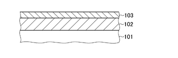
- FIG. 1A is a cross-sectional view showing a state of an intermediate process for explaining a method of manufacturing a mechanical vibrator in an embodiment of the present invention.
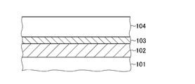
- FIG. 1B is a cross-sectional view showing the state of an intermediate step for explaining the method for manufacturing the mechanical vibrator in the embodiment of the present invention.
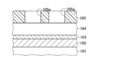
- FIG. 1C is a cross-sectional view showing a state of an intermediate step for explaining the method for manufacturing the mechanical vibrator in the embodiment of the present invention.
- FIG. 1D is a cross-sectional view showing the state of an intermediate step for explaining the method of manufacturing the mechanical vibrator in the embodiment of the present invention.
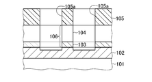
- FIG. 1E is a cross-sectional view showing a state of an intermediate step for explaining the method of manufacturing the mechanical vibrator in the embodiment of the present invention.
- FIG. 1F is a cross-sectional view showing a state of an intermediate step for explaining the method of manufacturing the mechanical vibrator in the embodiment of the present invention.
- FIG. 1G is a cross-sectional view showing the configuration of the mechanical vibrator in the embodiment of the present invention.
- FIG. 1H is a cross-sectional view showing the configuration of the mechanical vibrator in the embodiment of the present invention.
- FIGS. 1A to 1H a method for manufacturing a mechanical vibrator according to an embodiment of the present invention will be described with reference to FIGS. 1A to 1H.
- a nickel layer 102 made of a nickel crystal (single crystal) is formed on a substrate 101.
- a nickel layer 102 made of a nickel crystal is formed on a substrate 101.
- 200 nm of nickel is grown on the substrate 101 made of MgO to sufficiently relax the lattice.
- the plane orientation of the substrate 101 may not be specified.
- the substrate 101 is a single crystal, it may be a sapphire substrate, a nitride substrate, a SiC substrate, or a metal (which may be a nickel substrate or another metal substrate). And a material capable of withstanding the crystal growth temperature of diamond (around 1100 ° C.).
- the substrate temperature may be set to about 250 ° C. to about 450 ° C.
- nickel may be grown in a vacuum.
- Nickel may be formed by an electron beam evaporation method, a sputtering method, a molecular beam epitaxy method, a vapor deposition method using a nickel filament, or the like. Note that the optimum substrate temperature condition varies somewhat depending on the growth rate and growth method.
- the crystallinity of the nickel is improved by heating the substrate 101 to around 1000 ° C. in an atmosphere of hydrogen or under a vacuum with a hydrogen partial pressure of 5 Torr or more.
- a material layer 103 is formed by epitaxially growing a material composed of an element having no catalytic action on the nickel layer 102 (first step).
- the material layer 103 is formed by epitaxially growing iridium.
- iridium will be described as an example of an element having no catalytic action.
- the material layer 103 may be formed to a thickness of 1 atomic layer (0.3839 nm) or more and 10 nm or less on the sufficiently relaxed lattice of the nickel layer 102. Further, the material layer 103 may be formed thicker than 1 nm, for example, and the upper part in the thickness direction may be lattice-relaxed.
- the thickness of 1 nm is a critical thickness at which iridium does not cause lattice relaxation.
- the critical film thickness varies depending on the material and conditions. Note that a substrate made of single crystal nickel may be used as the nickel layer 102 without using the substrate 101.
- the lattice constant (in-plane lattice constant) in the plane direction of the material layer 103 having a thickness of 1 atomic layer is equal to the lattice constant of nickel (nickel layer 102), and strain is applied.
- the thickness becomes larger than the triatomic layer, the upper part of the material layer 103 gradually relaxes and the material layer 103 approaches the original lattice constant of iridium. Therefore, by controlling the thickness of the material layer 103 within a range in which the lattice is not completely relaxed, it is possible to form the material layer 103 in which the surface side (upper surface side) is moderately relaxed.
- the state of lattice relaxation depends on the thickness.
- the material layer 103 may be formed by growing iridium by an electron beam evaporation method, a sputtering method, a molecular beam epitaxy method, or the like. According to the molecular beam epitaxy method using a high-temperature knucell, the material layer 103 made of high-quality iridium can be obtained at a low growth rate.
- the material layer 103 made of iridium epitaxially grown on the nickel layer 102 made of single crystal nickel contains compressive strain in the plane, and the in-plane lattice constant is equal to that of nickel.
- the material layer 103 may be formed by depositing one atomic layer. However, in order to completely cover the surface of the nickel layer 102 industrially, it is more stable to deposit three or more layers.
- a cubic crystal is epitaxially grown on the material layer 103 to form a crystal layer 104 (second step).
- the crystal constituting the crystal layer 104 is diamond or cubic boron nitride.
- the in-plane lattice constant of the material layer 103 is equal to the lattice constant of the nickel layer 102.
- the crystal layer 104 epitaxially grown on the material layer 103 in this state is formed in the same manner as when epitaxially grown directly on the nickel layer 102, and has good crystallinity. In other words, the crystal layer 104 can be formed in a state where the lattice mismatch with the material layer 103 is eliminated.
- the in-plane lattice constant of the material layer 103 is slightly different from the lattice constant of the nickel layer 102 It becomes.
- the in-plane lattice constant of the crystal layer 104 is different from that of the nickel layer 102, and strain is applied.
- the strain applied to the crystal layer 104 made of cubic boron nitride or diamond can be controlled from the compressive strain to the tensile strain by epitaxially growing on the material layer 103 moderately lattice-relaxed. is there.
- a desired vibrator-shaped mask pattern 105 is formed on the crystal layer 104.
- the mask pattern 105 includes two openings 105a arranged at a predetermined interval.
- the mask pattern 105 may be formed by a known lithography technique.
- the mask pattern 105 may be made of any material, but the thickness is determined by the difference in etching rate with the crystal layer 104 to be processed and the thickness of the crystal layer 104.
- the laminated structure composed of the material layer 103 and the crystal layer 104 is patterned by an etching process using the mask pattern 105 as a mask to form the vibrator-shaped portion 106 (third step).
- the dry etching is physically performed to the depth reaching the nickel layer 102 from the two openings 105a by FIB using Ga ions or RIE using a mixed gas of oxygen and argon.
- FIGS. 1F and 1G a part of the nickel layer 102 below the vibrator-shaped portion 106 is removed to form a vibrator including the vibrator-shaped portion 106 (fourth step).
- FIG. 1G shows a cross section between two openings 105a in a direction different from FIG. 1F by 90 °.
- the nickel layer 102 may be etched by a predetermined amount by wet etching that selectively etches nickel using the vibrator-shaped portion 106 that has already been formed as a mask.
- the vibrator can be formed by selectively etching the nickel layer 102 through the two openings 105a with a hydrochloric acid aqueous solution or a dilute nitric acid aqueous solution.
- the nickel layer 102 below the material layer 103 is etched from both sides in a region between the two openings 105 a to form a space 102 a below the material layer 103.
- the vibrator-shaped portion 106 having a double-supported beam structure separated from the surface of the substrate 101 by the space 102a can be formed in the region between the two openings 105a.
- the vibrator shape portion 106 is in a state instructed by the nickel layers 102 on both sides of the space 102a in the left-right direction on the paper surface of FIG.
- the substrate itself is etched to a certain thickness from the back surface of the substrate 101 and the side surface of the substrate 101, but the characteristics of the vibrator itself are not affected.
- the mask pattern 105 is removed to form the material layer 103 made of iridium crystal and the material layer 103 as shown in FIG. 1H.
- a mechanical vibrator having a laminated structure including a crystal layer 104 made of cubic crystals is obtained.
- the lattice constant in the plane direction is made equal at the interface between the material layer 103 and the crystal layer 104.
- the crystal layer 104 is formed in a state where the lattice matches with the nickel layer 102 as described above.
- strain is applied to the crystal layer 104.
- vibration control can be performed by using the material layer 103 on the back surface as the other electrode and an electric field between these two electrodes.
- these two electrodes can be operated as a sensor by detecting an electric field generated by vibration.
- the surface-side electrode may be produced before the vibrator-shaped portion 106 is formed by etching, or may be produced after the vibrator-shaped portion 106 is formed.
- a crystal made of cubic boron nitride or diamond is epitaxially grown on the crystal layer 104 to form another crystal layer (not shown) (fifth step), and the material layer 103, the crystal layer 104, and the other crystal.
- the laminated structure composed of layers may be patterned to form the vibrator-shaped portion.
- iridium having a thickness of, for example, 10 nm or less is epitaxially grown on a nickel single crystal (nickel layer) to form a material layer, so that a lattice mismatch between diamond and cubic boron nitride epitaxially grown thereon is obtained. Therefore, hetero-growth on the material layer of high-quality diamond or cubic boron nitride (crystal) becomes possible.
- the material layer may be in a state in which the in-plane lattice constant of the nickel layer below is completely inherited, that is, in a state in which the compressive strain is completely applied, and by thickening the material layer, the material layer is partially latticed. It may be relaxed. That is, the strain state in the material layer can be controlled by the thickness of the material layer, and the strain applied to the crystal layer grown thereon can be controlled by this strain control.
- the thickness of the material layer may be one atomic layer, but industrially, it is desirable that a three-atom layer material layer exists. This also means that the nickel surface is prevented from being exposed due to partial defects, but it is often the case that the etching effect of the lower layer cannot be ignored in the process of growing the crystal layer.
- the surface of the nickel layer made of nickel needs to be covered with a material layer made of a material composed of an element having no catalytic action.
- a material composed of an element having no catalytic action platinum may be used in addition to iridium described above.
- the patterning of the crystal layer with diamond or cubic boron nitride does not require the substrate to be tilted, and the mask can be used to physically etch by FIB or RIE up to the depth reaching the nickel layer. .
- the etching rate of diamond or cubic boron nitride is slow, it can be solved by increasing the thickness of the mask formed on the surface.
- the nickel layer can be easily selectively etched with hydrochloric acid or dilute nitric acid, and is supported by a support such as a cantilever beam structure, a double-end beam structure, or a membrane structure with a crystal layer, and the vibration part is hollow.
- a vibrator having a floating structure can be manufactured.
- a thin iridium material layer is formed on the vibrating portion in a crystal layer made of diamond or cubic boron nitride.
- This material layer can be etched by high-temperature hydrofluoric acid. .
- the etching rate is extremely slow.
- the material layer is thin, so that the etching process can be performed in a realistic processing time.
- the nickel layer may be sufficiently lattice-relaxed, and the in-plane lattice constant may be the original nickel lattice constant.
- Lattice constant can be controlled. That is, by using a substrate having a lattice constant larger than that of nickel, it is possible to control lattice mismatch with diamond or cubic boron nitride within a range that does not impair crystallinity.
- the material layer made of iridium or platinum is completely lattice-relaxed, the lattice mismatch with the crystal layer becomes too large to form a crystal layer with good crystallinity. For this reason, it is important that the material layer has a thickness that does not completely relax the lattice, and the thickness is about 10 nm at the maximum.
- the lattice when the material layer is formed by epitaxially growing iridium on the nickel layer whose in-plane lattice constant is controlled, the lattice may be partially relaxed or partially relaxed as described above. .
- the thickness of the material layer epitaxially grown on the nickel layer is several layers that do not cause lattice relaxation. It is also good.
- the lattice mismatch with the crystal layer due to diamond or cubic boron nitride can be controlled by lattice relaxation of a part of the material layer on the surface side in the thickness direction.
- a cubic boron nitride layer or a diamond layer can be formed on the diamond or cubic boron nitride crystal layer epitaxially grown on the nickel layer.
- a single heterostructure composed of a diamond layer and a cubic boron nitride layer but also a superlattice in which a plurality of heterostructures are alternately laminated can be produced. Even in such a structure, it is possible to manufacture a vibrator by etching the nickel layer to a depth reaching the nickel layer and then selectively etching the nickel layer with hydrochloric acid, dilute nitric acid, or the like.
- An active element capable of controlling conductivity used as a gate electrode can be formed.
- Such a structure can be applied not only to the (001) plane and the (111) plane as the orientation of the growth plane, but it is easier to use the (001) plane when epitaxially growing diamond. .
- a material composed of a non-catalytic element is epitaxially grown on a nickel layer to form a material layer, and a cubic crystal is epitaxially grown on the material. Since the layers are formed, a high Q value can be obtained in a mechanical vibrator made of a cubic crystal such as diamond.
- Non-catalytic elements include iridium and platinum, but are not limited thereto.
Landscapes
- Chemical & Material Sciences (AREA)
- Engineering & Computer Science (AREA)
- Materials Engineering (AREA)
- Metallurgy (AREA)
- Organic Chemistry (AREA)
- Crystallography & Structural Chemistry (AREA)
- General Chemical & Material Sciences (AREA)
- Chemical Kinetics & Catalysis (AREA)
- Inorganic Chemistry (AREA)
- Mechanical Engineering (AREA)
- Crystals, And After-Treatments Of Crystals (AREA)
- Micromachines (AREA)
Abstract
ニッケル層(102)の上に触媒作用のない元素から構成された材料をエピタキシャル成長して材料層(103)を形成する。例えば、イリジウムをエピタキシャル成長して材料層(103)を形成する。次に、材料層(103)の上に立方晶の結晶をエピタキシャル成長して結晶層(104)を形成し、材料層(103)および結晶層(104)からなる積層構造をパターニングして振動子形状部(106)を形成する。材料層(103)の厚さは、完全に格子緩和しない範囲で制御する。
Description
本発明は、ダイアモンドまたは立方晶系窒化ホウ素などの立方晶の結晶から構成された機械振動子およびその製造方法に関する。
非常に高いヤング率を有するダイアモンドは、機械振動子として非常に高い周波数で動作することが可能である。機械振動子の振動部分にダイアモンドを用いようとする場合、選択的にエッチング除去が可能な層の上にダイアモンド層を形成し、ダイアモンド層の下の一部の基板を除去することで、梁構造を形成することになる。例えば、FIB(Focused Ion Beam)やRIE(Reactive Ion Etching)によって基板を傾けた状態で、物理的なドライエッチングによりエッチングした後、反対側に傾けて再び同様のエッチングをすることで、両側からエッチングして形成した開孔を連結させ、梁構造を作製することは原理上可能である。
しかしながらこの場合、ダイアモンド層の上に、一部の領域を保護するマスクを用いることになる。当然、ダイアモンド自体が非常に安定であるためエッチングレートは低く、エッチング過程でマスクも大幅にエッチングされることになり、実現したとしても加工サイズ、加工精度に限界がある。
一方、SiO2層を備えたSi基板上にCVD成長したダイアモンドを用いてダイアモンド機械振動子を形成する技術が提案されている(非特許文献1参照)。この技術では、SiO2層をフッ酸水溶液もしくはバッファーフッ酸水溶液によって選択的にウエットエッチングすることで、架橋構造や片持ち梁構造の作製を可能としている。しかし、Siとダイアモンドの格子定数差は50%以上もあり、Si上に高品質なダイアモンドを結晶成長すること自体が難しいことも知られている。
近年、イリジウム上のダイアモンドの薄膜成長が実現している(非特許文献2参照)。イリジウムは化学的に安定で、高温のフッ酸でエッチング可能であるものの、容易に選択エッチングが可能であるとは言い難い。また、イリジウムとダイアモンドの間に7パーセント以上の格子ミスマッチがあり、ホモエピタキシャルほどの品質は得られていない。振動する領域の結晶性が低いと、エネルギー散逸量が大きくなり、本来得られるはずのQ値を得ることができない。Q値が高ければ高いほど、低いエネルギーで動作が可能であり、またセンサーなどとして用いる場合、高感度とすることができる。このため、機械振動子には、結晶性のよい高品質な結晶を用いることが望まれる。
T. Shibata et al., "Micromachining of Diamond Film for MEMS Applications", Journal of Microelectromechanical Systems, vol. 9, no. 1, pp. 47-51, 2000.
鈴木 一博、澤邊 厚仁、「ダイヤモンドのヘテロエピタキシャル成長」、第59回応用物理学関係連合講演会 講演予稿集、15p-F5-2、244頁、2012年。
K. Hirama et al., "Heteroepitaxial growth of single-domain cubic boron nitride films by ion-beam-assisted MBE", Applied Physics Express, vol. 10, 035501, 2017.
H. Yamaguchi et al., "Improved resonance characteristics of GaAs beam resonators by epitaxially induced strain", Applied Physics Letters, vol. 92, no. 251913, 2008.
前述したように、ダイアモンドなどの結晶を用いることで、高い周波数で動作する機械振動子を構成することが可能であるが、結晶性のよい状態で振動子の構造を形成することが容易ではなく、結晶が備える高いヤング率による本来得られるはずの高いQ値を得ることが容易ではないという問題があった。
本発明は、以上のような問題点を解消するためになされたものであり、ダイアモンドなどの立方晶の結晶からなる機械振動子において、高いQ値が得られるようにすることを目的とする。
本発明に係る機械振動子の製造方法は、ニッケルの結晶からなるニッケル層の上に触媒作用のない元素から構成された材料をエピタキシャル成長して材料層を形成する第1工程と、材料層の上に立方晶の結晶をエピタキシャル成長して結晶層を形成する第2工程と、材料層および結晶層からなる積層構造をパターニングして振動子形状部を形成する第3工程と、振動子形状部の下部のニッケル層を除去して振動子形状部からなる振動子を形成する第4工程とを備える。
上記機械振動子の製造方法において、第1工程では、材料層を厚さ10nm以下に形成するとよい。
上記機械振動子の製造方法において、結晶層を構成する結晶は、ダイアモンドまたは立方晶系窒化ホウ素である。
上記機械振動子の製造方法において、第2工程では、材料層の上にダイアモンドまたは立方晶系窒化ホウ素からなる結晶をエピタキシャル成長して結晶層を形成し、更に、結晶層の上に立方晶系窒化ホウ素またはダイアモンドからなる結晶をエピタキシャル成長して他結晶層を形成する第5工程を備え、第3工程では、材料層,結晶層,および他結晶層からなる積層構造をパターニングして振動子形状部を形成してもよい。
上記機械振動子の製造方法において、触媒作用のない元素から構成された材料は、イリジウムまたは白金であればよい。
本発明に係る機械振動子は、触媒作用のない元素から構成された材料からなる材料層と、材料層の上に形成された立方晶の結晶からなる結晶層とを備える積層構造から構成され、材料層と結晶層との界面では、面方向の格子定数が等しい状態とされている。
上記機械振動子において、結晶層を構成する結晶は、ダイアモンドまたは立方晶系窒化ホウ素である。
上記機械振動子において、結晶層の上に立方晶系窒化ホウ素またはダイアモンドからなる他結晶層を備え、積層構造は、材料層、結晶層、および他結晶層から構成されているようにしてもよい。
上記機械振動子において、触媒作用のない元素から構成された材料は、イリジウムまたは白金であればよい。
以上説明したように、本発明によれば、ニッケルの結晶からなるニッケル層の上に触媒作用のない元素から構成された材料をエピタキシャル成長して材料層を形成し、この上に立方晶の結晶をエピタキシャル成長して結晶層を形成するようにしたので、ダイアモンドなどの立方晶の結晶からなる高いQ値の機械振動子が形成できるという優れた効果が得られる。
以下、本発明の実施の形態おける機械振動子の製造方法について図1A~図1Hを参照して説明する。
まず、図1Aに示すように、基板101の上にニッケルの結晶(単結晶)からなるニッケル層102を形成する。例えば、MgOからなる基板101上に、ニッケルを200nm成長し、十分に格子緩和させる。基板101の面方位は特定しなくてもよい。基板101は単結晶であれば、サファイア基板、窒化物基板、SiC基板、金属(ニッケル基板であっても、他の金属基板でもよい)であっても良いが、最終目的の立方晶系窒化ホウ素やダイアモンドの結晶成長温度(1100℃前後)に耐えることが可能な材料であることが必要である。
例えば、基板温度の条件を250℃から450℃前後とし、真空中でニッケルの成長を行えばよい。電子線蒸着法、スパッタ法、分子線エピタキシー法、ニッケルフィラメントによる蒸着法などによりニッケルを形成すればよい。なお、最適な基板温度の条件は、成長速度、成長方法によって多少異なる。ニッケルを成長した後、水素中もしくは真空下で水素分圧が5Torr以上の雰囲気下、基板101を1000℃前後に加熱することで、ニッケルの結晶性を向上させる。
次に、図1Bに示すように、ニッケル層102の上に触媒作用のない元素から構成された材料をエピタキシャル成長して材料層103を形成する(第1工程)。例えば、イリジウムをエピタキシャル成長して材料層103を形成する。以下では、触媒作用のない元素としてイリジウムを例に説明する。この場合、例えば、十分に格子緩和したニッケル層102の上に、厚さ1原子層(0.3839nm)以上10nm以下に材料層103を形成すればよい。また、材料層103は、例えば、1nmより厚く形成し、厚さ方向上部を格子緩和させてもよい。ここで、厚さ1nmは、イリジウムが格子緩和の生じない臨界膜厚である。なお、材料や条件により、臨界膜厚は変動する。なお、基板101を用いず、単結晶ニッケルによる基板をニッケル層102として用いてもよい。
厚さ1原子層の材料層103の面方向の格子定数(面内格子定数)は、ニッケル(ニッケル層102)の格子定数と等しくなり、歪が印加された状態となる。3原子層よりも厚くなるに従って、材料層103の上部は徐々に格子緩和し、材料層103はイリジウム本来の格子定数に近づいていく。従って、完全に格子緩和しない範囲で、材料層103の厚さを制御することで、表面側(上面側)が適度に格子緩和した材料層103を形成することができる。格子緩和の状態は、厚さによる。
例えば、電子線蒸着法、スパッタ法、分子線エピタキシー法などによりイリジウムを成長させることで、材料層103を形成すればよい。高温のクヌーセルを用いた分子線エピタキシー法によれば、成長速度は遅くなるが高品質なイリジウムからなる材料層103が得られる。
上述したように、単結晶のニッケルからなるニッケル層102の上にエピタキシャル成長したイリジウムによる材料層103は、面内に圧縮歪を含有し、面内格子定数はニッケルに等しくなる。材料層103は、1原子層を堆積させればよいが、工業的にはニッケル層102の表面を完全に被覆させるため、3層以上堆積させた方が安定である。
次に、図1Cに示すように、材料層103の上に立方晶の結晶をエピタキシャル成長して結晶層104を形成する(第2工程)。結晶層104を構成する結晶は、ダイアモンドまたは立方晶系窒化ホウ素である。前述したように、厚さ1原子層とした材料層103の上に結晶層104を形成した場合、材料層103の面内格子定数は、ニッケル層102の格子定数と等しくなる。この状態の材料層103の上にエピタキシャル成長した結晶層104は、ニッケル層102の上に直接エピタキシャル成長した場合と同様に形成され、結晶性のよいものとなる。言い換えると、材料層103との間の格子ミスマッチが解消された状態で結晶層104が形成できる。
また、完全に格子緩和しない範囲で1原子層より厚くした材料層103の上に結晶層104を形成した場合、材料層103の面内格子定数は、ニッケル層102の格子定数とは多少異なる状態となる。この場合、結晶層104の面内格子定数は、ニッケル層102とは異なる状態となり、歪みが印加されるものとなる。前述したように適度に格子緩和した材料層103の上にエピタキシャル成長することで、立方晶系窒化ホウ素やダイアモンドからなる結晶層104に印加される歪を圧縮歪から引っ張り歪まで制御することが可能である。
次に、図1Dに示すように、結晶層104の上に、所望とする振動子形状のマスクパターン105を形成する。例えば、マスクパターン105は、所定の間隔を開けて配置された2つの開口部105aを備えている。公知のリソグラフィー技術によりマスクパターン105を形成すればよい。マスクパターン105は、どのような材料から構成してもよいが、加工する結晶層104とのエッチングレートの差、結晶層104の厚さによって厚さを決定する。
次に、図1Eに示すように、マスクパターン105をマスクとしたエッチング処理により、材料層103および結晶層104からなる積層構造をパターニングして振動子形状部106を形成する(第3工程)。例えば、Gaイオンを用いたFIBや、酸素およびアルゴンの混合ガスを用いたRIEによって、2つの開口部105aより、ニッケル層102に到達する深さまで物理的にドライエッチングを行う。
次に、図1F,図1Gに示すように、振動子形状部106の下部のニッケル層102の一部を除去して振動子形状部106からなる振動子を形成する(第4工程)。図1Gは、図1Fとは、互いに90°異なる方向の、2つの開口部105aの間の断面を示している。例えば、すでに形成されている振動子形状部106をマスクとし、ニッケルを選択的にエッチングするウエットエッチングにより、ニッケル層102を所定量エッチングすればよい。
例えば、塩酸水溶液または希硝酸水溶液によって、2つの開口部105aを介し、ニッケル層102を選択的にエッチングすることで、振動子を形成することが可能である。このエッチングでは、2つの開口部105aの間の領域において、材料層103の下部のニッケル層102を両側部からエッチングし、材料層103の下部に空間102aを形成する。これにより、2つの開口部105aの間の領域に、空間102aにより基板101の表面より離間した両持ちの梁構造とされた振動子形状部106が形成できる。振動子形状部106は、図1Gの紙面左右方向において空間102aの両脇のニッケル層102に指示された状態となる。
なお、基板101の材料によっては、基板101の裏面、基板101の側面から基板自体も、ある程度の厚さがエッチングされることになるが、振動子自体の特性に影響はない。
以上のようにして、振動子形状部106を形成した後、マスクパターン105を除去することで、図1Hに示すように、イリジウムの結晶からなる材料層103と、材料層103の上に形成された立方晶の結晶からなる結晶層104とを備える積層構造から構成された機械振動子が得られる。この機械振動子では、材料層103と結晶層104との界面では、面方向の格子定数が等しい状態とされていることになる。材料層103の厚さを1原子層とした場合、前述したように、結晶層104は、ニッケル層102と格子がマッチした状態に形成されていることになる。一方、完全に格子緩和しない範囲で材料層103を1原子層より厚くした場合、結晶層104には、歪みが印加された状態となる。
このように形成した機械振動子の、上面に電極を形成すると、裏面の材料層103を他方の電極としこれら2つ電極の間の電界によって、振動制御が可能となる。また、これら2つの電極により、振動によって発生する電界を検出することでセンサーとしても動作させることができる。表面側の電極は、振動子形状部106をエッチングにより形成する前に作製してもよく、振動子形状部106を形成した後に作製しても良い。また、材料層103による裏面側の電極をバックゲートとして動作させつつ、振動によって結晶層104に生成したキャリアを変調させることも可能である。この場合、上面側に、結晶層104にオーミック接続する電極を形成することで、キャリアの変調が検出可能となる。
なお、結晶層104の上に、立方晶系窒化ホウ素またはダイアモンドからなる結晶をエピタキシャル成長して他結晶層(不図示)を形成し(第5工程)、材料層103,結晶層104,および他結晶層からなる積層構造をパターニングして振動子形状部を形成するようにしてもよい。
上述したように、ニッケル単結晶(ニッケル層)の上に、例えば10nm以下のイリジウムをエピタキシャル成長させて材料層とすることで、この上にエピタキシャル成長するダイアモンドおよび立方晶系窒化ホウ素との間の格子ミスマッチを制御することができ、高品質ダイアモンドや立方晶系窒化ホウ素(結晶)の材料層の上へのヘテロ成長が可能となる。
材料層は、この下のニッケル層の面内格子定数を完全に引き継いだ状態、つまり完全に圧縮歪を印加された状態でもよく、また材料層を厚くすることで、部分的に材料層を格子緩和させても良い。つまり、材料層の厚さにより材料層における歪の状態を制御することが可能となり、この歪み制御で、この上に成長する結晶層に印加される歪を制御することが可能となる。
ここで重要となるのは、材料層の上に結晶層をエピタキシャル成長する際、ニッケルと成長している結晶層とが反応しないだけの厚さをもつ材料層が形成されていることである。ニッケル層の全域を完全に材料層が覆っているのであれば、材料層の厚さは1原子層でもよいが、工業的には3原子層の材料層が存在することが望まれる。これは、部分的な欠陥によりニッケル表面が露出することを避ける意味もあるが、結晶層が成長する過程で、下層のエッチング効果が無視できないことが大きい。
例えば、ダイアモンドを成長させている表面にニッケルが存在すると、ニッケルの触媒作用によりグラファイトが形成されてしまう。また、窒化ホウ素を成長させている表面にニッケルが存在すると、立方晶ではなく六方晶系窒化ホウ素が形成されてしまう。このため、結晶層の成長においては、ニッケルからなるニッケル層の表面が、触媒作用のない元素から構成された材料による材料層で覆われている必要がある。触媒作用のない元素から構成された材料としては、前述したイリジウムの他に白金でもよい。
この構造において、ダイアモンドもしくは立方晶系窒化ホウ素による結晶層のパターニングでは、基板を傾ける必要が無く、マスクを用い、ニッケル層に到達する深さまでFIBやRIEで物理的にエッチングすることが可能となる。また、ダイアモンドもしくは立方晶系窒化ホウ素のエッチングレートは遅いものの、表面に形成するマスクを厚くすることで解決できる。ニッケル層は、塩酸、希硝酸で容易に選択エッチングすることが可能であり、結晶層による片持ちの梁構造、両持ちの梁構造、メンブレン構造など、支持部により支持され、振動部分が中空に浮いた構造による振動子を作製することが可能となる。
ここで、振動部分には、ダイアモンドもしくは立方晶系窒化ホウ素からなる結晶層に、薄いイリジウムによる材料層が形成されているが、この材料層は、高温のフッ酸によってエッチングすることが可能である。材料層を、側方(断面方向)からエッチングする場合、極めてエッチングレートが遅いが、表面側からのエッチングであれば、材料層は薄いため、現実的な加工時間でエッチング処理が可能となる。
半導体や異種の単結晶金属からなる基板の上にエピタキシャル成長した単結晶のニッケルによるニッケル層を用いても、ニッケル層まで到達する加工を施した後に、前述したように選択的にエッチングすることで、容易に振動子を作製できる。単純には、ニッケル層が十分に格子緩和し、面内格子定数が本来のニッケルの格子定数となっていても良いが、格子緩和を意図的に不完全とすることで、最表面の面内格子定数を制御できる。つまり、ニッケルよりも大きな格子定数を持つ基板を用いることで、結晶性を損なわない範囲で、ダイアモンドまたは立方晶系窒化ホウ素との間の格子ミスマッチを制御することが可能となる。なお、イリジウムや白金からなる材料層の表面が完全に格子緩和していると、結晶層との間の格子のミスマッチが大きくなりすぎ、結晶性のよい結晶層が形成できなくなる。このため、材料層は、完全に格子緩和しない範囲の厚さとすることが重要であり、最大でも厚さ10nm程度とする。
このように、面内格子定数を制御したニッケル層の上にイリジウムをエピタキシャル成長して材料層を形成する際、前述の通り完全に歪んだ状態であっても部分的に格子緩和していても良い。
単独のニッケル層、もしくは半導体や異種の単結晶金属基板上のニッケル層のいずれの場合も、前述したように、ニッケル層の上にエピタキシャル成長する材料層の厚さは、格子緩和が生じない数層としても良い。当然、ニッケル層と同様に、材料層の厚さ方向表面側の一部を格子緩和させることで、ダイアモンドや立方晶系窒化ホウ素による結晶層との格子ミスマッチを制御することが可能である。
すなわち、ニッケル層、材料層のどちらも残留歪量を制御することで、結晶層に圧縮歪や引っ張り歪みを印加することが可能である。このようにして結晶層に歪を印加すると、振動子としての特性も制御することが可能である。一般的には、振動部分に引っ張り歪を与えた場合、高周波数で動作し、高いQ値の振動子を得ることができる(非特許文献4参照)。
また、ニッケル層の上にエピタキシャル成長したダイアモンドまたは立方晶系窒化ホウ素による結晶層の上には、互いに、立方晶系窒化ホウ素の層またはダイアモンドの層(他結晶層)を形成することが可能であるが。この場合、ダイアモンド層と立方晶系窒化ホウ素層によるシングルヘテロ構造はもちろん、交互に複数のヘテロ構造を積層する超格子も作製可能となる。このような構造においても、ニッケル層まで到達する深さまでエッチングした後、ニッケル層を塩酸や希硝酸などで選択的にエッチングすることで振動子の作製が可能となる。
上述したようなダイアモンド層(結晶層)と窒化ホウ素層(他結晶層)とのヘテロ構造や、窒化ホウ素でダイアモンド層の両面を挟んだダイアモンド量子井戸構造を作製すると、ニッケル層や材料層をバックゲート電極として用いた伝導性制御が可能な能動素子を構成することができる。このような構造は、成長面の方位としては(001)面、(111)面に限らずあらゆる面に応用できるが、ダイアモンドをエピタキシャル成長する場合は(001)面を用いた場合がより容易である。
以上に説明したように、本発明によれば、ニッケル層の上に触媒作用のない元素から構成された材料をエピタキシャル成長して材料層を形成し、この上に立方晶の結晶をエピタキシャル成長して結晶層を形成するようにしたので、ダイアモンドなどの立方晶の結晶からなる機械振動子において、高いQ値が得られるようになる。触媒作用のない元素としては、イリジウムや白金などがあるが、これに限られるものではない。
なお、本発明は以上に説明した実施の形態に限定されるものではなく、本発明の技術的思想内で、当分野において通常の知識を有する者により、多くの変形および組み合わせが実施可能であることは明白である。
101…基板、102…ニッケル層、102a…空間、103…材料層、104…結晶層、105…マスクパターン、105a…開口部、106…振動子形状部。
Claims (8)
- ニッケルの結晶からなるニッケル層の上に触媒作用のない元素から構成された材料をエピタキシャル成長して材料層を形成する第1工程と、
前記材料層の上に立方晶の結晶をエピタキシャル成長して結晶層を形成する第2工程と、
前記材料層および前記結晶層からなる積層構造をパターニングして振動子形状部を形成する第3工程と、
前記振動子形状部の下部の前記ニッケル層を除去して前記振動子形状部からなる振動子を形成する第4工程と
を備えることを特徴とする機械振動子の製造方法。 - 請求項1記載の機械振動子の製造方法において、
前記第1工程では、前記材料層を厚さ10nm以下に形成することを特徴とする機械振動子の製造方法。 - 請求項1または2記載の機械振動子の製造方法において、
前記結晶層を構成する結晶は、ダイアモンドまたは立方晶系窒化ホウ素である
ことを特徴とする機械振動子の製造方法。 - 請求項3記載の機械振動子の製造方法において、
前記第2工程では、前記材料層の上にダイアモンドまたは立方晶系窒化ホウ素からなる結晶をエピタキシャル成長して前記結晶層を形成し、
更に、前記結晶層の上に立方晶系窒化ホウ素またはダイアモンドからなる結晶をエピタキシャル成長して他結晶層を形成する第5工程を備え、
前記第3工程では、前記材料層,前記結晶層,および前記他結晶層からなる積層構造をパターニングして前記振動子形状部を形成する
ことを特徴とする機械振動子の製造方法。 - 請求項1~4のいずれか1項に記載の機械振動子の製造方法において、
前記材料は、イリジウムまたは白金であることを特徴とする機械振動子の製造方法。 - 触媒作用のない元素から構成された材料からなる材料層と、
前記材料層の上に形成された立方晶の結晶からなる結晶層と
を備える積層構造から構成され、
前記材料層と前記結晶層との界面では、面方向の格子定数が等しい状態とされている
ことを特徴とする機械振動子。 - 請求項5記載の機械振動子において、
前記結晶層を構成する結晶は、ダイアモンドまたは立方晶系窒化ホウ素である
ことを特徴とする機械振動子。 - 請求項6または7記載の機械振動子において、
前記材料は、イリジウムまたは白金であることを特徴とする機械振動子。
Priority Applications (1)
| Application Number | Priority Date | Filing Date | Title |
|---|---|---|---|
| US16/973,706 US12049711B2 (en) | 2018-06-11 | 2019-05-20 | Method for producing a mechanical vibrator comprising epitaxially growing a cubic crystal on a material layer to form a laminate structure which is patterned to form a vibrator shape part |
Applications Claiming Priority (2)
| Application Number | Priority Date | Filing Date | Title |
|---|---|---|---|
| JP2018-110928 | 2018-06-11 | ||
| JP2018110928A JP7077798B2 (ja) | 2018-06-11 | 2018-06-11 | 機械振動子およびその製造方法 |
Publications (1)
| Publication Number | Publication Date |
|---|---|
| WO2019239803A1 true WO2019239803A1 (ja) | 2019-12-19 |
Family
ID=68842840
Family Applications (1)
| Application Number | Title | Priority Date | Filing Date |
|---|---|---|---|
| PCT/JP2019/019896 Ceased WO2019239803A1 (ja) | 2018-06-11 | 2019-05-20 | 機械振動子およびその製造方法 |
Country Status (3)
| Country | Link |
|---|---|
| US (1) | US12049711B2 (ja) |
| JP (1) | JP7077798B2 (ja) |
| WO (1) | WO2019239803A1 (ja) |
Cited By (1)
| Publication number | Priority date | Publication date | Assignee | Title |
|---|---|---|---|---|
| JP6998634B1 (ja) | 2020-10-22 | 2022-01-18 | 国立大学法人長岡技術科学大学 | ダイヤモンド形成用構造体、およびダイヤモンド形成用構造体の製造方法 |
Citations (2)
| Publication number | Priority date | Publication date | Assignee | Title |
|---|---|---|---|---|
| WO2007092893A2 (en) * | 2006-02-07 | 2007-08-16 | Target Technology Company, Llc | Materials and methods for the manufacture of large crystal diamonds |
| JP2011168460A (ja) * | 2010-02-22 | 2011-09-01 | National Institute For Materials Science | 単結晶ダイヤモンド・エアギャップ構造体及びその作製方法 |
Family Cites Families (2)
| Publication number | Priority date | Publication date | Assignee | Title |
|---|---|---|---|---|
| US5298286A (en) * | 1992-11-09 | 1994-03-29 | North Carolina State University | Method for fabricating diamond films on nondiamond substrates and related structures |
| CN204958378U (zh) * | 2015-08-28 | 2016-01-13 | 深圳力策科技有限公司 | 一种类金刚石碳微悬梁臂 |
-
2018
- 2018-06-11 JP JP2018110928A patent/JP7077798B2/ja active Active
-
2019
- 2019-05-20 WO PCT/JP2019/019896 patent/WO2019239803A1/ja not_active Ceased
- 2019-05-20 US US16/973,706 patent/US12049711B2/en active Active
Patent Citations (2)
| Publication number | Priority date | Publication date | Assignee | Title |
|---|---|---|---|---|
| WO2007092893A2 (en) * | 2006-02-07 | 2007-08-16 | Target Technology Company, Llc | Materials and methods for the manufacture of large crystal diamonds |
| JP2011168460A (ja) * | 2010-02-22 | 2011-09-01 | National Institute For Materials Science | 単結晶ダイヤモンド・エアギャップ構造体及びその作製方法 |
Non-Patent Citations (1)
| Title |
|---|
| Y UYA MOCHIMARU ET AL.: "Fabrication and evaluation of CVD diamond resonators", PROCEEDINGS OF THE 16TH INTERNATIONAL CONFERENCE ON NANOTECHNOLOG Y, 25 August 2016 (2016-08-25), pages 676 - 677, XP033003859, DOI: 10.1109/NANO.2016.7751555 * |
Cited By (2)
| Publication number | Priority date | Publication date | Assignee | Title |
|---|---|---|---|---|
| JP6998634B1 (ja) | 2020-10-22 | 2022-01-18 | 国立大学法人長岡技術科学大学 | ダイヤモンド形成用構造体、およびダイヤモンド形成用構造体の製造方法 |
| JP2022068862A (ja) * | 2020-10-22 | 2022-05-10 | 国立大学法人長岡技術科学大学 | ダイヤモンド形成用構造体、およびダイヤモンド形成用構造体の製造方法 |
Also Published As
| Publication number | Publication date |
|---|---|
| US20210207286A1 (en) | 2021-07-08 |
| US12049711B2 (en) | 2024-07-30 |
| JP7077798B2 (ja) | 2022-05-31 |
| JP2019214484A (ja) | 2019-12-19 |
Similar Documents
| Publication | Publication Date | Title |
|---|---|---|
| KR100438467B1 (ko) | 박막 공진기 장치 및 이의 제조 방법 | |
| JP7114786B2 (ja) | ダイヤモンドおよびダイヤモンドのヘテロエピタキシャル形成法 | |
| US9656859B2 (en) | Method for fabricating suspended MEMS structures | |
| TW201344946A (zh) | 外延結構體 | |
| JP5454283B2 (ja) | 窒化ガリウム系エピタキシャル成長基板及びその製造方法並びにこの基板を用いて製造される電界効果型トランジスタ | |
| TWI477665B (zh) | 外延結構體的製備方法 | |
| CN101273438B (zh) | 薄膜元件的制造方法 | |
| TW201343537A (zh) | 外延結構體 | |
| KR20170102129A (ko) | 나노 로드 제조방법 | |
| US8906487B2 (en) | Base material with single-crystal silicon carbide film, method of producing single-crystal silicon carbide film, and method of producing base material with single-crystal silicon carbide film | |
| US12049711B2 (en) | Method for producing a mechanical vibrator comprising epitaxially growing a cubic crystal on a material layer to form a laminate structure which is patterned to form a vibrator shape part | |
| CN116346067A (zh) | 空腔型体声波谐振器及其制作方法 | |
| JP6922840B2 (ja) | 光デバイス構造およびその作製方法 | |
| JP5030163B2 (ja) | 微小機械共振器およびその製造方法 | |
| JP6988710B2 (ja) | 2次元材料デバイスの作製方法 | |
| JP2012204602A (ja) | 立方晶炭化珪素膜の製造方法 | |
| JP3754294B2 (ja) | 炭化珪素単結晶基板の製造方法及び半導体装置の製造方法 | |
| JPH11112099A (ja) | 半導体光素子の作製方法 | |
| JP6032759B2 (ja) | 微細機械共振器の作製方法 | |
| US12362724B2 (en) | N-polar rare-earth III-nitride bulk acoustic wave resonator | |
| JP6085235B2 (ja) | 機械共振器の作製方法 | |
| JP6748033B2 (ja) | カーボンチューブの製造方法 | |
| JP2015013352A (ja) | 微細機械構造の作製方法 | |
| JP2018037561A (ja) | 炭化珪素基体の製造方法 | |
| KR20150144579A (ko) | 반도체 소자 제조 방법 |
Legal Events
| Date | Code | Title | Description |
|---|---|---|---|
| 121 | Ep: the epo has been informed by wipo that ep was designated in this application |
Ref document number: 19819963 Country of ref document: EP Kind code of ref document: A1 |
|
| NENP | Non-entry into the national phase |
Ref country code: DE |
|
| 122 | Ep: pct application non-entry in european phase |
Ref document number: 19819963 Country of ref document: EP Kind code of ref document: A1 |