WO2019239648A1 - 撮像装置及び内視鏡 - Google Patents
撮像装置及び内視鏡 Download PDFInfo
- Publication number
- WO2019239648A1 WO2019239648A1 PCT/JP2019/007605 JP2019007605W WO2019239648A1 WO 2019239648 A1 WO2019239648 A1 WO 2019239648A1 JP 2019007605 W JP2019007605 W JP 2019007605W WO 2019239648 A1 WO2019239648 A1 WO 2019239648A1
- Authority
- WO
- WIPO (PCT)
- Prior art keywords
- image sensor
- identification information
- control signal
- clock
- control
- Prior art date
- Legal status (The legal status is an assumption and is not a legal conclusion. Google has not performed a legal analysis and makes no representation as to the accuracy of the status listed.)
- Ceased
Links
Images



Classifications
-
- A—HUMAN NECESSITIES
- A61—MEDICAL OR VETERINARY SCIENCE; HYGIENE
- A61B—DIAGNOSIS; SURGERY; IDENTIFICATION
- A61B1/00—Instruments for performing medical examinations of the interior of cavities or tubes of the body by visual or photographical inspection, e.g. endoscopes; Illuminating arrangements therefor
- A61B1/04—Instruments for performing medical examinations of the interior of cavities or tubes of the body by visual or photographical inspection, e.g. endoscopes; Illuminating arrangements therefor combined with photographic or television appliances
- A61B1/045—Control thereof
-
- G—PHYSICS
- G02—OPTICS
- G02B—OPTICAL ELEMENTS, SYSTEMS OR APPARATUS
- G02B23/00—Telescopes, e.g. binoculars; Periscopes; Instruments for viewing the inside of hollow bodies; Viewfinders; Optical aiming or sighting devices
- G02B23/24—Instruments or systems for viewing the inside of hollow bodies, e.g. fibrescopes
Definitions
- the present invention relates to an imaging apparatus and an endoscope that can individually control a plurality of imaging elements.
- bus standard communication standard
- I2C Inter-Integrated Circuit
- asynchronous 1-Wire registered trademark
- a master device that requests data reading and writing, and a slave device that receives data and sends data in response to a request from the master device. Further, a plurality of slave devices are connected to one master device, and the master device can control the plurality of slave devices.
- individual identification numbers for example, 64-bit IDs
- the master device individually controls the plurality of slave devices by giving an identification number to a control signal transmitted to the slave device.
- the present invention has been made in view of the above circumstances, and an object of the present invention is to provide an imaging apparatus and an endoscope that can give identification information from a master device to a slave device after the manufacture of an electronic device.
- the imaging device of one embodiment of the present invention receives a control unit that outputs a control signal for controlling an imaging element and the control signal to which the same identification information as the first identification information held by the imaging unit is received,
- the first image sensor that operates based on the control signal and the control signal to which the same identification information as the second identification information held by itself is received
- the second image sensor that operates based on the control signal.
- a clock circuit capable of individually supplying clocks for driving the first and second imaging elements, and the control unit uses the clock circuit to generate the first imaging element.
- the clock is supplied to In the state where the supply of the clock to the second image sensor is stopped, the control signal for giving the first identification information is transmitted, and the first image sensor is transmitted by the clock circuit.
- the control signal for giving the second identification information is transmitted, and the first image sensor Receives the control signal for giving the first identification information in the driving state, and operates to hold the first identification information, and the second image sensor is in the driving state, the second image sensor When the control signal for giving the identification information of 2 is received, the second identification information is held.
- the first and second imaging elements included in the imaging device according to the one aspect are provided at a distal end portion of the insertion portion.
- An imaging apparatus includes a control unit that transmits a control signal via a connected first control line, and the control signal that is transmitted from the control unit via the first control line. And receiving the control signal to which the same identification information as the first identification information held by itself is given, is transmitted through the connected second control line.
- a first image sensor that operates based on the control signal, and an element that receives the control signal transmitted from the first image sensor via the second control line, and is held by itself When the control signal to which the same identification information as the second identification information is given is received, the second image sensor that operates based on the control signal is connected to the first and second image sensors, And driving the first and second image sensors.
- a clock circuit capable of individually supplying a clock for causing the clock to be supplied to the first image sensor by the clock circuit, and for the clock to the second image sensor.
- the control signal for giving the first identification information is transmitted, the clock circuit stops the supply of the clock to the first image sensor, and the first
- the control signal for giving the second identification information is transmitted in a state where the clock is supplied to the second image sensor, and the first image sensor transmits the first identification information in the drive state.
- the control signal for giving is received, the first identification information is operated to hold, and the second imaging element gives the second identification information in a driving state. Upon receiving the said control signal, it operates to hold the second identification information.
- the first and second imaging elements provided in the imaging device according to the other aspect are provided at a distal end portion of the insertion portion.
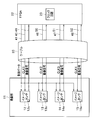
- FIG. 1 is a diagram illustrating an example of an overall configuration of an endoscope system including an imaging device according to the first embodiment.
- FIG. 2 illustrates an imaging unit, a cable, and an FPGA according to the first embodiment. It is a figure for demonstrating a detailed structure.
- an endoscope system 1 includes an endoscope 2 as an imaging device, a processor 3, and a monitor 4.
- the endoscope 2 transmits to the imaging unit 11, an imaging unit 11 provided at the distal end of the insertion unit to be inserted into the subject, an imaging signal transmitted from the imaging unit 11, a clock transmitted to the imaging unit 11, and the imaging unit 11.
- the cable 20 which transmits a control signal etc. and the connector 21 provided in the base end side of the cable 20 are provided.
- the endoscope 2 is configured to be detachably connected to the processor 3 via a connector 21.
- the connector 21 is provided with an FPGA (Field Programmable Gate Array) 22.
- the FPGA 22 has a clock circuit 23.
- the FPGA 22 transmits a control signal and the like to the imaging unit 11 and receives an imaging signal transmitted from the imaging unit 11.
- the FPGA 22 outputs the input imaging signal to the image processing unit 31.
- the clock circuit 23 provided in the FPGA 22 can generate clocks CLK1, CLK2, CLK3, and CLK4, which will be described later, and supply them to the imaging unit 11.
- the endoscope 2 includes an operation unit (not shown) on the proximal end side of the elongated insertion unit.
- the operation section is provided with a bending operation knob for bending the bending section provided in the insertion section, various operation switches for performing various operations of the endoscope 2, and the like.
- the processor 3 includes an image processing unit 31.
- the image processing unit 31 performs predetermined image processing on the imaging signal output from the FPGA 22 to generate a video signal, and outputs the video signal to the monitor 4.
- the monitor 4 displays the video signal from the image processing unit 31.
- the imaging unit 11 includes a plurality (four in the present embodiment) of image sensors 12, 13, 14, and 15.
- the imaging unit 11 includes four image sensors 12, 13, 14, and 15.
- the present invention is not limited to this, and for example, two, three, or five or more image sensors are included. You may have.
- the image sensors 12, 13, 14, and 15 that are slave devices can receive data and send data in response to a request from the FPGA 22 that is a master device.
- the FPGA 22 as the master device is provided in the connector 21 of the endoscope 2, but may be provided in the operation unit of the endoscope 2 or the processor 3, for example.
- the image sensors 12, 13, 14 and 15 have registers 12a, 13a, 14a and 15a, respectively.
- the registers 12a, 13a, 14a, and 15a can hold various data such as control data and device ID, which will be described later, transmitted to the image sensors 12, 13, 14, and 15, respectively.
- the FPGA 22 as a control unit is connected to the image sensors 12, 13, 14 and 15 via a control line 41 as a first control line.
- the image sensors 12, 13, 14, and 15 of the present embodiment are connected in parallel through the control line 41 in the imaging unit 11.
- the image sensor 12 as the first image sensor can receive control data (control signal) transmitted from the FPGA 22 via the control line 41.
- the image sensor 13 as the second image sensor can receive control data (control signal) transmitted from the FPGA 22 via the control line 41.
- the image sensor 14 can receive control data (control signal) transmitted from the FPGA 22 via the control line 41.
- the image sensor 15 can receive control data (control signal) transmitted from the FPGA 22 via the control line 41.
- the FPGA 22 is connected to the image sensors 12, 13, 14 and 15 via clock signal lines 45, 46, 47 and 48, respectively.
- the FPGA 22 can transmit clocks CLK1, CLK2, CLK3, and CLK4 to the image sensors 12, 13, 14, and 15 using the clock signal lines 45, 46, 47, and 48, respectively.
- the FPGA 22 is connected to the image sensors 12, 13, 14 and 15 via the imaging signal lines 49, 50, 51 and 52, respectively.
- Each of the image sensors 12, 13, 14, and 15 can transmit an imaging signal obtained by imaging a subject to the FPGA 22 via the imaging signal lines 49, 50, 51, and 52.
- the cable 20 that connects the FPGA 22 and the imaging unit 11 includes the control line 41 for transmitting the control data, the clock signal lines 45 to 48 for transmitting the clocks CLK1 to CLK4, and the imaging signal. Imaging signal lines 49 to 52 for transmission are provided.
- the cable 20 is also provided with a power line and a GND line (not shown).
- the FPGA 22 transmits control data to the image sensors 12, 13, 14, and 15 using the control line 41.
- This control data is data for controlling the image sensor 12, 13, 14 or 15.
- the image sensors 12, 13, 14 and 15 cannot recognize whether the control data is the control data transmitted to itself. Therefore, in this embodiment, every time the power of the processor 3 is turned on, the FPGA 22 performs a process of writing a device ID into the registers 12a, 13a, 14a, and 15a of the image sensors 12, 13, 14, and 15.
- the FPGA 22 adds the device ID of the image sensor 12, 13, 14 or 15 to be transmitted to the control data and transmits it.
- the image sensors 12, 13, 14 and 15 detect whether the control data is transmitted to itself by referring to the device ID added to the control data. Capture control data. As a result, the FPGA 22 can individually control the image sensors 12, 13, 14 and 15.
- FIG. 3 is a flowchart for explaining an example of a process flow for writing a device ID to the image sensors 12 to 15, and FIG. 4 explains an example of a process flow for writing a device ID to the image sensors 12 to 15. It is a timing chart for. Note that the processing in FIG. 3 is executed each time the power of the processor 3 is turned on.
- the FPGA 22 outputs the clock CLK1 and the device ID for the image sensor 12 (S1). At this time, the FPGA 22 stops the clocks CLK2, CLK3, and CLK4. The clock CLK1 is transmitted to the image sensor 12 via the clock signal line 45. The device ID for the image sensor 12 as control data is transmitted to the image sensor 12 via the control line 41.
- the FPGA 22 transmits a device ID (“0001”) for the image sensor 12, which is first identification information, to the image sensor 12 using the control line 41. Accordingly, the image sensor 12 writes the device ID for the image sensor 12 as the first identification information in the register 12a based on the clock CLK1.
- the FPGA 22 outputs the clock CLK2 and the device ID for the image sensor 13 (S2). At this time, the FPGA 22 stops the clocks CLK1, CLK3, and CLK4. The clock CLK2 is transmitted to the image sensor 13 via the clock signal line 46. The device ID for the image sensor 13 as control data is transmitted to the image sensor 13 via the control line 41.
- the FPGA 22 transmits a device ID (“0010”) for the image sensor 13, which is second identification information, to the image sensor 13 using the control line 41.
- the image sensor 13 writes the device ID for the image sensor 13 as the second identification information in the register 13a based on the clock CLK2.
- the FPGA 22 outputs the clock CLK3 and the device ID for the image sensor 14 (S3). At this time, the FPGA 22 stops the clocks CLK1, CLK2, and CLK4. The clock CLK3 is transmitted to the image sensor 14 via the clock signal line 47. Further, the device ID for the image sensor 14 as control data is transmitted to the image sensor 14 via the control line 41.
- the FPGA 22 transmits a device ID (“0011”) for the image sensor 14, which is third identification information, to the image sensor 14 using the control line 41.
- the image sensor 14 writes the device ID for the image sensor 14 as the third identification information in the register 14a based on the clock CLK3.
- the FPGA 22 outputs the clock CLK4 and the device ID for the image sensor 15 (S4). At this time, the FPGA 22 stops the clocks CLK1, CLK2, and CLK3. The clock CLK4 is transmitted to the image sensor 15 via the clock signal line 48. The device ID for the image sensor 15 as control data is transmitted to the image sensor 15 via the control line 41.
- the FPGA 22 transmits a device ID (“0100”) for the image sensor 15, which is fourth identification information, to the image sensor 15 using the control line 41.
- the image sensor 15 writes the device ID for the image sensor 15 as the fourth identification information in the register 15a based on the clock CLK4.
- the FPGA 22 determines whether or not device IDs are written in all the image sensors 12 to 15 (S5).
- the FPGA 22 refers to the header information of the data (imaging signal) transmitted from the image sensors 12, 13, 14, and 15, for example, so that the device ID is normally written in the image sensors 12, 13, 14, and 15. Determine whether or not.
- the process returns to S1. On the other hand, if the FPGA 22 determines that the device IDs have been written in all the image sensors 12 to 15 (S5: YES), it ends the process.
- the FPGA 22 when transmitting control data for designating an exposure time to the image sensor 13, for example, the FPGA 22 has a device ID of the device to be transmitted (in this example, an image in this example).
- the device ID “0010”) of the sensor 13 is added.
- data for designating the exposure time in this example, “11111010” is added after the device ID.
- Such control data is transmitted to the image sensors 12, 13, 14 and 15 through the control line 41.
- the FPGA 22 supplies the clocks CLK1, CLK2, CLK3, and CLK4 to the image sensors 12, 13, 14, and 15 via the clock signal lines 45, 46, 47, and 48, respectively.
- the image sensor 13 recognizes that it is the control data transmitted to itself by referring to the device ID included in the control data, and takes in the control data. As a result, the image sensor 13 can capture the subject image with the exposure time specified (set) by the FPGA 22.
- control data and the clock CLK1 are also supplied to the image sensor 12, the image sensor 12 does not capture the control data because the device ID included in the control data is not its own device ID. Similarly, the image sensors 14 and 15 do not capture control data because the device ID included in the control data is not its own device ID.
- the FPGA 22 can assign device IDs to the image sensors 12, 13, 14 and 15, respectively, and can control the image sensors 12, 13, 14 and 15 individually.
- identification information can be given from the master device to the slave device after the electronic device is manufactured.
- one control line 41 for transmitting control data is provided between the FPGA 22 and the image sensors 12, 13, 14, and 15.
- one control line for transmitting control data from the FPGA 22 to the image sensors 12 to 15 of the imaging unit 11 can be provided in the cable 20, and the cable 20 and the cable 20 are inserted.
- the insertion part of the endoscope 2 can be reduced in diameter.
- the processing of FIG. 3 is executed every time the power of the processor 3 is turned on, and the device ID is written in the registers 12a to 15a of the image sensors 12 to 15.
- this is not limitative.
- the processing of FIG. 3 is not performed each time the processor 3 is powered on. May be.
- the image sensors 12, 13, 14, and 15 each include a nonvolatile memory
- the image sensors 12, 13, 14, and 15 each have a nonvolatile memory even when the power supply to the endoscope 2 is turned off.
- the device ID written in can be held. Therefore, if the process of FIG. 3 is executed only once after the endoscope 2 is manufactured, the image sensors 12, 13, 14 and 15 can each hold their own device ID even when the power is turned off. it can.
- FIG. 5 is a flowchart for explaining another example of the process flow of writing the device ID into the image sensors 12 to 15.
- the same processes as those in FIG. 5 are identical processes as those in FIG. 5.
- the FPGA 22 determines whether device IDs are written in all the image sensors 12 to 15 (S11).
- the FPGA 22 determines whether or not a device ID is written in the image sensors 12, 13, 14, and 15 by referring to header information of data transmitted from the image sensors 12, 13, 14, and 15, for example.
- the FPGA 22 determines that the device IDs are not written in all the image sensors 12 to 15 (S11: NO) If the FPGA 22 determines that the device IDs are not written in all the image sensors 12 to 15 (S11: NO), the FPGA 22 proceeds to the process of S1. That is, if the FPGA 22 determines that the device IDs are not written in all the image sensors 12 to 15, the FPGA 22 writes the device IDs in the image sensors 12 to 15 (S1 to S4) and the devices in the image sensors 12 to 15 A determination process (S5) of whether or not the ID has been normally written is performed.
- the FPGA 22 determines that the device IDs are written in all the image sensors 12 to 15 (S11: YES), the process is terminated. That is, when each of the image sensors 12 to 15 has a nonvolatile memory and the device ID is written in each of the nonvolatile memories of the image sensors 12 to 15, the FPGA 22 assigns the device ID to the image sensors 12 to 15.
- the processing ends without performing the writing processing (S1 to S4) and the determination processing (S5) of whether or not the device ID is normally written in the image sensors 12 to 15.
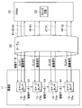
- FIG. 6 is a diagram for explaining a detailed configuration of the imaging unit, the cable, and the FPGA according to the second embodiment.
- the same components as those in FIG. 6 are identical to FIG. 6, the same components as those in FIG.
- the FPGA 22 as a control unit is connected to the image sensor 12 via a control line 41 as a first control line.
- the image sensor 12 is connected to the image sensor 13 through a control line 42 as a second control line. Further, the image sensor 13 is connected to the image sensor 14 via the control line 43, and the image sensor 14 is connected to the image sensor 15 via the control line 44.
- the image sensors 12, 13, 14, and 15 of this embodiment are connected in series to the FPGA 22 via the control lines 41, 42, 43, and 44.
- the image sensor 12 as the first image sensor can receive control data (control signal) transmitted from the FPGA 22 via the control line 41.
- the image sensor 13 as the second image sensor can receive control data transmitted from the image sensor 12 via the control line 42.
- the image sensor 14 can receive control data transmitted from the image sensor 13 via the control line 43.
- the image sensor 15 can receive control data transmitted from the image sensor 14 via the control line 44.
- the FPGA 22 transmits control data to the image sensor 12 using the control line 41.
- This control data is data for controlling the image sensor 12, 13, 14 or 15.
- the image sensor 12 transmits control data to the image sensor 13 using the control line 42. Further, the image sensor 13 transmits control data to the image sensor 14 using the control line 43. Further, the image sensor 14 transmits control data to the image sensor 15 using the control line 44.
- the image sensors 12, 13, 14 and 15 cannot recognize whether the control data is the control data transmitted to itself. Therefore, in this embodiment, every time the power of the processor 3 is turned on, the FPGA 22 performs a process of writing a device ID into the registers 12a, 13a, 14a, and 15a of the image sensors 12, 13, 14, and 15.
- the FPGA 22 adds the device ID of the image sensor 12, 13, 14 or 15 to be transmitted to the control data and transmits it.
- the image sensors 12, 13, 14 and 15 detect whether the control data is transmitted to itself by referring to the device ID added to the control data. Capture control data. As a result, the FPGA 22 can individually control the image sensors 12, 13, 14 and 15.
- the FPGA 22 can allocate device IDs to the image sensors 12, 13, 14, and 15, respectively, and can control the image sensors 12, 13, 14, and 15 individually.
- identification information can be given from the master device to the slave device after manufacturing the electronic device, as in the first embodiment.
- the image sensors 12, 13, 14, and 15 are each configured to include a nonvolatile memory instead of the registers 12a, 13a, 14a, and 15a, as in the modification of the first embodiment, the image sensors 12, 13, A process of writing its own device ID only once in the nonvolatile memory included in each of 14 and 15 may be performed.
- each step in the flowchart in the present specification may be executed in a different order for each execution by changing the execution order and performing a plurality of steps at the same time as long as it does not contradict its nature.
Landscapes
- Physics & Mathematics (AREA)
- Health & Medical Sciences (AREA)
- Life Sciences & Earth Sciences (AREA)
- Optics & Photonics (AREA)
- Surgery (AREA)
- Biomedical Technology (AREA)
- Animal Behavior & Ethology (AREA)
- Radiology & Medical Imaging (AREA)
- Nuclear Medicine, Radiotherapy & Molecular Imaging (AREA)
- Engineering & Computer Science (AREA)
- Biophysics (AREA)
- Heart & Thoracic Surgery (AREA)
- Medical Informatics (AREA)
- Molecular Biology (AREA)
- Pathology (AREA)
- General Health & Medical Sciences (AREA)
- Public Health (AREA)
- Veterinary Medicine (AREA)
- Astronomy & Astrophysics (AREA)
- General Physics & Mathematics (AREA)
- Endoscopes (AREA)
- Instruments For Viewing The Inside Of Hollow Bodies (AREA)
Abstract
撮像装置は、FPGA22と、イメージセンサ12と、イメージセンサ13と、クロック回路23とを備る。FPGA22は、イメージセンサ12にクロックが供給され、かつ、イメージセンサ13にクロックの供給が停止されている状態において、第1の識別情報を付与するための制御信号を送信し、イメージセンサ12にクロックの供給が停止され、かつ、イメージセンサ13にクロックが供給されている状態において、第2の識別情報を付与するための制御信号を送信し、イメージセンサ12は、第1の識別情報を付与するための制御信号を受信すると、第1の識別情報を保持し、イメージセンサ13は、第2の識別情報を付与するための前記制御信号を受信すると、第2の識別情報を保持する。
Description
本発明は、複数の撮像素子を個別に制御することができる撮像装置及び内視鏡に関する。
従来、データの伝送を行うバス規格(通信規格)として、同期式のI2C(Inter-Integrated Circuit)、あるいは、非同期式の1-Wire(登録商標)等が存在する。
これらの通信方式では、データの読み取り及び書き込みの要求を行うマスターデバイスと、マスターデバイスの要求に応じてデータを受け取る及びデータを送出するスレーブデバイスとが設けられる。さらに、1つのマスターデバイスに対して複数のスレーブデバイスを接続され、マスターデバイスは、複数のスレーブデバイスを制御可能となっている。
1つのマスターデバイスが複数のスレーブデバイスを個別に制御するために、複数のスレーブデバイスのそれぞれに個別の識別番号(例えば64ビットID)が登録されている。マスターデバイスは、複数のスレーブデバイスを個別に制御する際に、スレーブデバイスに送信する制御信号に識別番号を付与することで、複数のスレーブデバイスを個別に制御している。
しかしながら、マスターデバイスと複数のスレーブデバイスとが搭載された電子機器を製造する際に、製造されるそれぞれの電子機器に対して、スレーブデバイスの識別番号をマスターデバイスに登録する作業を行わなければならなかった。そのため、電子機器の製造に係る工数が増加する要因となっている。
本発明は、上記事情に鑑みてなされたもので、電子機器の製造後において、マスターデバイスからスレーブデバイスへ識別情報を付与することができる撮像装置及び内視鏡を提供することを目的とする。
本発明の一態様の撮像装置は、撮像素子を制御する制御信号を出力する制御部と、自身が保持する第1の識別情報と同一の識別情報が付与された前記制御信号を受信すると、前記制御信号に基づいて動作する第1の撮像素子と、自身が保持する第2の識別情報と同一の識別情報が付与された前記制御信号を受信すると、前記制御信号に基づいて動作する第2の撮像素子と、前記制御部から出力された前記制御信号を前記第1の撮像素子及び前記第2の撮像素子に対して伝送する制御線と、前記第1及び前記第2の撮像素子に接続され、かつ、前記第1及び前記第2の撮像素子に対して駆動させるためのクロックを個別に供給可能なクロック回路と、を備え、前記制御部は、前記クロック回路により、前記第1の撮像素子にクロックが供給され、かつ、前記第2の撮像素子にクロックの供給が停止されている状態において、前記第1の識別情報を付与するための前記制御信号を送信し、前記クロック回路により、前記第1の撮像素子にクロックの供給が停止され、かつ、前記第2の撮像素子にクロックが供給されている状態において、前記第2の識別情報を付与するための前記制御信号を送信し、前記第1の撮像素子は、駆動状態において前記第1の識別情報を付与するための前記制御信号を受信すると、前記第1の識別情報を保持するように動作し、前記第2の撮像素子は、駆動状態において前記第2の識別情報を付与するための前記制御信号を受信すると、前記第2の識別情報を保持するように動作する。
また、本発明の一態様の内視鏡は、上記一態様の前記撮像装置が備える前記第1及び前記第2の撮像素子が、挿入部の先端部に設けられている。
本発明の他の態様の撮像装置は、接続される第1の制御線を介して制御信号を送信する制御部と、前記第1の制御線を介して前記制御部から送信される前記制御信号を受信し、接続される第2の制御線を介して前記制御信号を送信する素子であって、自身が保持する第1の識別情報と同一の識別情報が付与された前記制御信号を受信すると、前記制御信号に基づいて動作する第1の撮像素子と、前記第2の制御線を介して前記第1の撮像素子から送信された前記制御信号を受信する素子であって、自身が保持する第2の識別情報と同一の識別情報が付与された前記制御信号を受信すると、前記制御信号に基づいて動作する第2の撮像素子と、前記第1及び前記第2の撮像素子に接続され、かつ、前記第1及び前記第2の撮像素子に対して駆動させるためのクロックを個別に供給可能なクロック回路と、を備え、前記制御部は、前記クロック回路により、前記第1の撮像素子にクロックが供給され、かつ、前記第2の撮像素子にクロックの供給が停止されている状態において、前記第1の識別情報を付与するための前記制御信号を送信し、前記クロック回路により、前記第1の撮像素子にクロックの供給が停止され、かつ、前記第2の撮像素子にクロックが供給されている状態において、前記第2の識別情報を付与するための前記制御信号を送信し、前記第1の撮像素子は、駆動状態において前記第1の識別情報を付与するための前記制御信号を受信すると、前記第1の識別情報を保持するように動作し、前記第2の撮像素子は、駆動状態において前記第2の識別情報を付与するための前記制御信号を受信すると、前記第2の識別情報を保持するように動作する。
また、本発明の他の態様の内視鏡は、上記他の態様の前記撮像装置が備える前記第1及び前記第2の撮像素子が、挿入部の先端部に設けられている。
以下、図面を参照して本発明の実施形態を説明する。
(第1の実施形態)
図1は、第1の実施形態に係わる撮像装置を備えた内視鏡システムの全体構成の一例を説明する図であり、図2は、第1の実施形態に係わる撮像部、ケーブル及びFPGAの詳細な構成を説明するための図である。
図1は、第1の実施形態に係わる撮像装置を備えた内視鏡システムの全体構成の一例を説明する図であり、図2は、第1の実施形態に係わる撮像部、ケーブル及びFPGAの詳細な構成を説明するための図である。
図1に示すように、内視鏡システム1は、撮像装置としての内視鏡2と、プロセッサ3と、モニタ4とを有して構成されている。
内視鏡2は、被検体に挿入される挿入部の先端部に設けられた撮像部11と、撮像部11から送信される撮像信号、撮像部11に送信するクロック、撮像部11に送信する制御信号等を伝送するケーブル20と、ケーブル20の基端側に設けられたコネクタ21とを備える。内視鏡2は、コネクタ21を介してプロセッサ3に着脱自在に接続されるように構成されている。
コネクタ21には、FPGA(Field Programmable Gate Array)22が設けられている。FPGA22は、クロック回路23を有している。FPGA22は、撮像部11に対して制御信号等を送信するとともに、撮像部11から送信された撮像信号が入力される。FPGA22は、入力された撮像信号を画像処理部31に出力する。
FPGA22に設けられたクロック回路23は、後述するクロックCLK1、CLK2、CLK3及びCLK4を生成し、撮像部11に供給することができる。また、内視鏡2は、細長の挿入部の基端側に図示しない操作部を備える。この操作部には、挿入部に設けられた湾曲部を湾曲操作させるための湾曲操作ノブ、及び、内視鏡2の各種操作を行うための各種操作スイッチ等が設けられている。
プロセッサ3は、画像処理部31を有して構成されている。画像処理部31は、FPGA22から出力された撮像信号に対して所定の画像処理を施して映像信号を生成し、モニタ4に出力する。モニタ4は、画像処理部31からの映像信号を表示する。
図2に示すように、撮像部11は、複数(本実施形態では4つ)のイメージセンサ12、13、14及び15を有している。なお、撮像部11は、4つのイメージセンサ12、13、14及び15を有しているが、これに限定されることなく、例えば、2つ、3つ、あるいは、5つ以上のイメージセンサを有していてもよい。
スレーブデバイスであるイメージセンサ12、13、14及び15は、マスターデバイスであるFPGA22の要求に応じてデータを受け取る及びデータを送出することができる。なお、マスターデバイスであるFPGA22は、内視鏡2のコネクタ21に設けられているが、例えば、内視鏡2の操作部、あるいは、プロセッサ3に設けられていてもよい。
また、イメージセンサ12、13、14及び15は、それぞれレジスタ12a、13a、14a及び15aを有している。レジスタ12a、13a、14a及び15aは、イメージセンサ12、13、14及び15のそれぞれに送信された後述する制御データ及びデバイスID等の各種データを保持することができる。
制御部としてのFPGA22は、第1の制御線としての制御線41を介してイメージセンサ12、13、14及び15に接続されている。このように、本実施形態のイメージセンサ12、13、14及び15は、撮像部11内において制御線41を介して並列接続されている。
第1の撮像素子としてのイメージセンサ12は、FPGA22から制御線41を介して送信された制御データ(制御信号)を受信することができる。また、第2の撮像素子としてのイメージセンサ13は、FPGA22から制御線41を介して送信された制御データ(制御信号)を受信することができる。また、イメージセンサ14は、FPGA22から制御線41を介して送信された制御データ(制御信号)を受信することができる。さらに、また、イメージセンサ15は、FPGA22から制御線41を介して送信された制御データ(制御信号)を受信することができる。
また、FPGA22は、クロック信号線45、46、47及び48を介してイメージセンサ12、13、14及び15にそれぞれ接続されている。FPGA22は、クロック信号線45、46、47及び48を用いて、イメージセンサ12、13、14及び15にクロックCLK1、CLK2、CLK3及びCLK4をそれぞれ送信することができる。
また、FPGA22は、撮像信号線49、50、51及び52を介してイメージセンサ12、13、14及び15にそれぞれ接続されている。イメージセンサ12、13、14及び15は、それぞれ被写体を撮像した撮像信号を撮像信号線49、50、51及び52を介してFPGA22に送信することができる。
このように、FPGA22と撮像部11とを接続するケーブル20には、制御データを送信するための制御線41、クロックCLK1~CLK4を送信するためのクロック信号線45~48、及び、撮像信号を送信するための撮像信号線49~52が設けられている。なお、ケーブル20には、図示しない電源線及びGND線も設けられている。
FPGA22は、制御線41を用いて制御データをイメージセンサ12、13、14及び15に送信する。この制御データは、イメージセンサ12、13、14または15を制御するためのデータである。
このとき、イメージセンサ12、13、14及び15は、制御データが自身に送信された制御データかを認識できない。そのため、本実施形態では、プロセッサ3の電源がONされる度に、FPGA22がイメージセンサ12、13、14及び15のレジスタ12a、13a、14a及び15aにデバイスIDを書き込む処理を行う。
そして、FPGA22は、送信対象となるイメージセンサ12、13、14または15のデバイスIDを制御データに付加して送信する。イメージセンサ12、13、14及び15は、制御データに付加されたデバイスIDを参照することで、自身に送信された制御データか否かを検出し、自身に送信された制御データの場合、その制御データを取り込む。これにより、FPGA22は、イメージセンサ12、13、14及び15を個別に制御することができるようになっている。
次に、このように構成された内視鏡2がイメージセンサ12~15にデバイスIDを書き込む動作について説明する。
図3は、イメージセンサ12~15にデバイスIDを書き込む処理の流れの一例を説明するためのフローチャートであり、図4は、イメージセンサ12~15にデバイスIDを書き込む処理の流れの一例を説明するためのタイミングチャートである。なお、図3の処理は、プロセッサ3の電源がONされる度に実行される。
まず、プロセッサ3の電源がONされ、内視鏡2に電源が供給されると、FPGA22は、クロックCLK1及びイメージセンサ12用のデバイスIDを出力する(S1)。このとき、FPGA22は、クロックCLK2、CLK3、CLK4を停止している。クロックCLK1は、クロック信号線45を介してイメージセンサ12に送信される。また、制御データとしてのイメージセンサ12用のデバイスIDは、制御線41を介してイメージセンサ12に送信される。
より具体的には、図4に示すように、FPGA22は、制御線41を用いて第1の識別情報であるイメージセンサ12用のデバイスID("0001")をイメージセンサ12に送信する。これにより、イメージセンサ12は、クロックCLK1に基づいて、第1の識別情報であるイメージセンサ12用のデバイスIDをレジスタ12aに書き込む。
次に、FPGA22は、クロックCLK2及びイメージセンサ13用のデバイスIDを出力する(S2)。このとき、FPGA22は、クロックCLK1、CLK3、CLK4を停止している。クロックCLK2は、クロック信号線46を介してイメージセンサ13に送信される。また、制御データとしてのイメージセンサ13用のデバイスIDは、制御線41を介してイメージセンサ13に送信される。
より具体的には、図4に示すように、FPGA22は、制御線41を用いて第2の識別情報であるイメージセンサ13用のデバイスID("0010")をイメージセンサ13に送信する。これにより、イメージセンサ13は、クロックCLK2に基づいて、第2の識別情報であるイメージセンサ13用のデバイスIDをレジスタ13aに書き込む。
次に、FPGA22は、クロックCLK3及びイメージセンサ14用のデバイスIDを出力する(S3)。このとき、FPGA22は、クロックCLK1、CLK2、CLK4を停止している。クロックCLK3は、クロック信号線47を介してイメージセンサ14に送信される。また、制御データとしてのイメージセンサ14用のデバイスIDは、制御線41を介してイメージセンサ14に送信される。
より具体的には、図4に示すように、FPGA22は、制御線41を用いて第3の識別情報であるイメージセンサ14用のデバイスID("0011")をイメージセンサ14に送信する。これにより、イメージセンサ14は、クロックCLK3に基づいて、第3の識別情報であるイメージセンサ14用のデバイスIDをレジスタ14aに書き込む。
次に、FPGA22は、クロックCLK4及びイメージセンサ15用のデバイスIDを出力する(S4)。このとき、FPGA22は、クロックCLK1、CLK2、CLK3を停止している。クロックCLK4は、クロック信号線48を介してイメージセンサ15に送信される。また、制御データとしてのイメージセンサ15用のデバイスIDは、制御線41を介してイメージセンサ15に送信される。
より具体的には、図4に示すように、FPGA22は、制御線41を用いて第4の識別情報であるイメージセンサ15用のデバイスID("0100")をイメージセンサ15に送信する。これにより、イメージセンサ15は、クロックCLK4に基づいて、第4の識別情報であるイメージセンサ15用のデバイスIDをレジスタ15aに書き込む。
最後に、FPGA22は、全てのイメージセンサ12~15にデバイスIDが書き込まれたか否かを判定する(S5)。FPGA22は、例えば、イメージセンサ12、13、14及び15から送信されたデータ(撮像信号)のヘッダ情報を参照することで、イメージセンサ12、13、14及び15にデバイスIDが正常に書き込まれたか否かを判定する。
FPGA22は、全てのイメージセンサ12~15にデバイスIDが書き込まれていないと判定した場合(S5:NO)、S1の処理に戻る。一方、FPGA22は、全てのイメージセンサ12~15にデバイスIDが書き込まれたと判定した場合(S5:YES)、処理を終了する。
図4に示すように、FPGA22は、例えばイメージセンサ13に対して露光時間を指定するための制御データを送信する場合、制御データの先頭に送信対象であるデバイスのデバイスID(この例では、イメージセンサ13のデバイスIDである"0010")を付加する。そして、デバイスIDの後に露光時間を指定するためのデータ(この例では、"11111010")を付加する。
このような制御データは、制御線41を介してイメージセンサ12、13、14及び15に送信される。また、FPGA22は、クロック信号線45、46、47及び48を介してクロックCLK1、CLK2、CLK3及びCLK4のそれぞれをイメージセンサ12、13、14及び15に供給する。
イメージセンサ13は、制御データに含まれるデバイスIDを参照することで、自身に送信された制御データであることを認識し、制御データを取り込む。これにより、イメージセンサ13は、FPGA22によって指定(設定)された露光時間で被写体像を撮像することができる。
イメージセンサ12にも制御データ及びクロックCLK1が供給されているが、イメージセンサ12は、制御データに含まれるデバイスIDが自身のデバイスIDではないため、制御データを取り込むことがない。同様に、イメージセンサ14及び15は、制御データに含まれるデバイスIDが自身のデバイスIDではないため、制御データを取り込むことがない。
以上の処理により、FPGA22は、イメージセンサ12、13、14及び15にそれぞれデバイスIDを割り振ることができ、イメージセンサ12、13、14及び15を個別に制御することができる。
よって、本実施形態の内視鏡システムによれば、電子機器の製造後において、マスターデバイスからスレーブデバイスへ識別情報を付与することができる。
また、従来では、調歩同期式で複数のイメージセンサ12~15を制御する場合、調歩同期式ではチップセレクト信号が存在しないため、FPGA22とイメージセンサ12~15との間に制御データを送信する制御線がそれぞれ設けられていた。
これに対し、本実施形態では、FPGA22とイメージセンサ12、13、14及び15との間に制御データを送信する制御線41が1本設けられている。
この結果、本実施形態では、FPGA22から撮像部11のイメージセンサ12~15に制御データを送信する制御線をケーブル20内において1本にすることができ、ケーブル20及びケーブル20が挿通される内視鏡2の挿入部を細径化することができる。
(変形例)
上述した実施形態では、プロセッサ3の電源が投入される度に図3の処理を実行し、イメージセンサ12~15のレジスタ12a~15aにデバイスIDを書き込んでいたが、これ限定されることはない。例えば、イメージセンサ12、13、14及び15がレジスタ12a、13a、14a及び15aに代わりそれぞれ不揮発性メモリを備える構成の場合、プロセッサ3の電源が投入される度に図3の処理を実行しなくてもよい。
上述した実施形態では、プロセッサ3の電源が投入される度に図3の処理を実行し、イメージセンサ12~15のレジスタ12a~15aにデバイスIDを書き込んでいたが、これ限定されることはない。例えば、イメージセンサ12、13、14及び15がレジスタ12a、13a、14a及び15aに代わりそれぞれ不揮発性メモリを備える構成の場合、プロセッサ3の電源が投入される度に図3の処理を実行しなくてもよい。
イメージセンサ12、13、14及び15がそれぞれ不揮発性メモリを備えている場合、イメージセンサ12、13、14及び15は、内視鏡2への電源の供給がOFFされても、それぞれ不揮発性メモリに書き込まれたデバイスIDを保持することができる。そのため、内視鏡2の製造後に1回だけ図3の処理を実行すれば、イメージセンサ12、13、14及び15は、電源がOFFされた場合でも、それぞれ自身のデバイスIDを保持することができる。
図5は、イメージセンサ12~15にデバイスIDを書き込む処理の流れの他の例を説明するためのフローチャートである。なお、図5において、図3と同一の処理については同一の符号を付して説明を省略する。
まず、プロセッサ3の電源がONされ、内視鏡2に電源が供給されると、FPGA22は、全てのイメージセンサ12~15にデバイスIDが書き込まれているか否かを判定する(S11)。FPGA22は、例えば、イメージセンサ12、13、14及び15から送信されたデータのヘッダ情報を参照することで、イメージセンサ12、13、14及び15にデバイスIDが書き込まれたか否かを判定する。
FPGA22は、全てのイメージセンサ12~15にデバイスIDが書き込まれていない判定した場合(S11:NO)、S1の処理に進む。すなわち、FPGA22は、全てのイメージセンサ12~15にデバイスIDが書き込まれていない判定した場合、イメージセンサ12~15にデバイスIDを書き込む処理(S1~S4)、及び、イメージセンサ12~15にデバイスIDが正常に書き込まれたか否かの判定処理(S5)を行う。
一方、FPGA22は、全てのイメージセンサ12~15にデバイスIDが書き込まれていると判定した場合(S11:YES)、処理を終了する。すなわち、イメージセンサ12~15がそれぞれ不揮発性メモリを有し、イメージセンサ12~15の不揮発性メモリにそれぞれデバイスIDが書き込まれている状態の場合、FPGA22は、イメージセンサ12~15にデバイスIDを書き込む処理(S1~S4)、及び、イメージセンサ12~15にデバイスIDが正常に書き込まれたか否かの判定処理(S5)を行わずに、処理を終了する。
以上の処理により、イメージセンサ12~15にデバイスIDを書き込む必要がない場合、S1~S5の処理を行わないため、上述した実施形態よりもプロセッサ3の電源が投入された際の内視鏡2の処理量を軽減させることができる。
(第2の実施形態)
次に、第2の実施形態について説明する。
次に、第2の実施形態について説明する。
図6は、第2の実施形態に係わる撮像部、ケーブル及びFPGAの詳細な構成を説明するための図である。なお、図6において、図2と同様の構成については、同一の符号を付して説明を省略する。
制御部としてのFPGA22は、第1の制御線としての制御線41を介してイメージセンサ12に接続されている。また、イメージセンサ12は、第2の制御線としての制御線42を介してイメージセンサ13と接続されている。さらに、イメージセンサ13は、制御線43を介してイメージセンサ14と接続され、イメージセンサ14は、制御線44を介してイメージセンサ15と接続されている。このように、本実施形態のイメージセンサ12、13、14及び15は、制御線41、42、43及び44を介してFPGA22に直列接続されている。
第1の撮像素子としてのイメージセンサ12は、FPGA22から制御線41を介して送信された制御データ(制御信号)を受信することができる。また、第2の撮像素子としてのイメージセンサ13は、イメージセンサ12から制御線42を介して送信された制御データを受信することができる。また、イメージセンサ14は、イメージセンサ13から制御線43を介して送信された制御データを受信することができる。さらに、また、イメージセンサ15は、イメージセンサ14から制御線44を介して送信された制御データを受信することができる。
FPGA22は、制御線41を用いて制御データをイメージセンサ12に送信する。この制御データは、イメージセンサ12、13、14または15を制御するためのデータである。イメージセンサ12は、制御線42を用いて制御データをイメージセンサ13に送信する。また、イメージセンサ13は、制御線43を用いて制御データをイメージセンサ14に送信する。さらに、イメージセンサ14は、制御線44を用いて制御データをイメージセンサ15に送信する。
このとき、イメージセンサ12、13、14及び15は、制御データが自身に送信された制御データかを認識できない。そのため、本実施形態では、プロセッサ3の電源がONされる度に、FPGA22がイメージセンサ12、13、14及び15のレジスタ12a、13a、14a及び15aにデバイスIDを書き込む処理を行う。
そして、FPGA22は、送信対象となるイメージセンサ12、13、14または15のデバイスIDを制御データに付加して送信する。イメージセンサ12、13、14及び15は、制御データに付加されたデバイスIDを参照することで、自身に送信された制御データか否かを検出し、自身に送信された制御データの場合、その制御データを取り込む。これにより、FPGA22は、イメージセンサ12、13、14及び15を個別に制御することができるようになっている。
なお、イメージセンサ12、13、14及び15のレジスタ12a、13a、14a及び15aにデバイスIDを書き込む処理については、図3の処理と同様のため、説明を省略する。
以上により、FPGA22は、イメージセンサ12、13、14及び15にそれぞれデバイスIDを割り振ることができ、イメージセンサ12、13、14及び15を個別に制御することができる。
よって、本実施形態の内視鏡システムによれば、第1の実施形態と同様に、電子機器の製造後において、マスターデバイスからスレーブデバイスへ識別情報を付与することができる。
なお、イメージセンサ12、13、14及び15がレジスタ12a、13a、14a及び15aに代わりそれぞれ不揮発性メモリを備える構成の場合、第1の実施形態の変形例と同様に、イメージセンサ12、13、14及び15のそれぞれが備える不揮発性メモリに自身のデバイスIDを1回だけ書き込む処理を行うようにしてもよい。
なお、本明細書におけるフローチャート中の各ステップは、その性質に反しない限り、実行順序を変更し、複数同時に実行し、あるいは実行毎に異なった順序で実行してもよい。
本発明は、上述した実施形態に限定されるものではなく、本発明の要旨を変えない範囲において、種々の変更、改変等が可能である。
本出願は、2018年6月11日に日本国に出願された特願2018-111327号を優先権主張の基礎として出願するものであり、上記の開示内容は、本願明細書、請求の範囲に引用されるものとする。
Claims (16)
- 撮像素子を制御する制御信号を出力する制御部と、
自身が保持する第1の識別情報と同一の識別情報が付与された前記制御信号を受信すると、前記制御信号に基づいて動作する第1の撮像素子と、
自身が保持する第2の識別情報と同一の識別情報が付与された前記制御信号を受信すると、前記制御信号に基づいて動作する第2の撮像素子と、
前記制御部から出力された前記制御信号を前記第1の撮像素子及び前記第2の撮像素子に対して伝送する制御線と、
前記第1及び前記第2の撮像素子に接続され、かつ、前記第1及び前記第2の撮像素子に対して駆動させるためのクロックを個別に供給可能なクロック回路と、
を備え、
前記制御部は、
前記クロック回路により、前記第1の撮像素子にクロックが供給され、かつ、前記第2の撮像素子にクロックの供給が停止されている状態において、前記第1の識別情報を付与するための前記制御信号を送信し、
前記クロック回路により、前記第1の撮像素子にクロックの供給が停止され、かつ、前記第2の撮像素子にクロックが供給されている状態において、前記第2の識別情報を付与するための前記制御信号を送信し、
前記第1の撮像素子は、駆動状態において前記第1の識別情報を付与するための前記制御信号を受信すると、前記第1の識別情報を保持するように動作し、
前記第2の撮像素子は、駆動状態において前記第2の識別情報を付与するための前記制御信号を受信すると、前記第2の識別情報を保持するように動作する、
ことを特徴とする撮像装置。 - 前記第1の撮像素子にクロックが供給されて、かつ、前記第2の撮像素子にクロックの供給が停止されている状態において、
前記第1の撮像素子は、前記制御部から送信される前記第1の識別情報を付与するための前記制御信号を認識して、自身の識別情報として前記第1の識別情報を保持し、
前記第2の撮像素子は、前記制御部から送信されて前記第1の撮像素子を通過した前記第1の識別情報を付与するための前記制御信号を認識しない、
ことを特徴とする請求項1に記載の撮像装置。 - 前記第1の撮像素子にクロックの供給が停止されて、かつ、前記第2の撮像素子にクロックが供給されている状態において、
前記第1の撮像素子は、前記制御部から送信された前記第2の識別情報を付与するための前記制御信号を認識せず、
前記第2の撮像素子は、前記制御部から送信されて前記第1の撮像素子を通過した前記第2の識別情報を付与するための前記制御信号を認識して、自身の識別情報として前記第2の識別情報を保持する、
ことを特徴とする請求項2に記載の撮像装置。 - 前記制御部は、電源が投入された際に、前記第1及び前記第2の撮像素子がそれぞれ前記第1及び前記第2の識別情報を保持しているか否かを判定し、前記第1及び前記第2の撮像素子がそれぞれ前記第1及び前記第2の識別情報を保持していないと判定した場合、前記クロック回路により前記第1の識別情報を付与するための前記制御信号及び前記第2の識別情報を付与するための前記制御信号のそれぞれを前記第1及び前記第2の撮像素子に送信する、
ことを特徴とする請求項1に記載の撮像装置。 - 前記制御部は、前記電源が投入された際に、前記第1及び前記第2の撮像素子がそれぞれ前記第1及び前記第2の識別情報を保持していると判定した場合、前記クロック回路により前記第1の識別情報を付与するための前記制御信号及び前記第2の識別情報を付与するための前記制御信号のそれぞれを前記第1及び前記第2の撮像素子に送信しない、
ことを特徴とする請求項4に記載の撮像装置。 - 請求項1に記載の前記撮像装置が備える前記第1及び前記第2の撮像素子は、挿入部の先端部に設けられている、
ことを特徴とする内視鏡。 - 前記第1の制御線は、前記第1及び前記第2の撮像素子が設けられている前記先端部と、前記挿入部の湾曲操作を行う操作部と、を繋ぐ細長の前記挿入部の内部に配設されている、
ことを特徴とする請求項6に記載の内視鏡。 - 前記第2の制御線は、前記第1及び前記第2の撮像素子が設けられている前記先端部の内部に配設されている、
ことを特徴とする請求項7に記載の内視鏡。 - 接続される第1の制御線を介して制御信号を送信する制御部と、
前記第1の制御線を介して前記制御部から送信される前記制御信号を受信し、接続される第2の制御線を介して前記制御信号を送信する素子であって、自身が保持する第1の識別情報と同一の識別情報が付与された前記制御信号を受信すると、前記制御信号に基づいて動作する第1の撮像素子と、
前記第2の制御線を介して前記第1の撮像素子から送信された前記制御信号を受信する素子であって、自身が保持する第2の識別情報と同一の識別情報が付与された前記制御信号を受信すると、前記制御信号に基づいて動作する第2の撮像素子と、
前記第1及び前記第2の撮像素子に接続され、かつ、前記第1及び前記第2の撮像素子に対して駆動させるためのクロックを個別に供給可能なクロック回路と、
を備え、
前記制御部は、
前記クロック回路により、前記第1の撮像素子にクロックが供給され、かつ、前記第2の撮像素子にクロックの供給が停止されている状態において、前記第1の識別情報を付与するための前記制御信号を送信し、
前記クロック回路により、前記第1の撮像素子にクロックの供給が停止され、かつ、前記第2の撮像素子にクロックが供給されている状態において、前記第2の識別情報を付与するための前記制御信号を送信し、
前記第1の撮像素子は、駆動状態において前記第1の識別情報を付与するための前記制御信号を受信すると、前記第1の識別情報を保持するように動作し、
前記第2の撮像素子は、駆動状態において前記第2の識別情報を付与するための前記制御信号を受信すると、前記第2の識別情報を保持するように動作する、
ことを特徴とする撮像装置。 - 前記第1の撮像素子にクロックが供給されて、かつ、前記第2の撮像素子にクロックの供給が停止されている状態において、
前記第1の撮像素子は、前記制御部から送信される前記第1の識別情報を付与するための前記制御信号を認識して、自身の識別情報として前記第1の識別情報を保持し、
前記第2の撮像素子は、前記制御部から送信されて前記第1の撮像素子を通過した前記第1の識別情報を付与するための前記制御信号を認識しない、
ことを特徴とする請求項9に記載の撮像装置。 - 前記第1の撮像素子にクロックの供給が停止されて、かつ、前記第2の撮像素子にクロックが供給されている状態において、
前記第1の撮像素子は、前記制御部から送信された前記第2の識別情報を付与するための前記制御信号を認識せず、
前記第2の撮像素子は、前記制御部から送信されて前記第1の撮像素子を通過した前記第2の識別情報を付与するための前記制御信号を認識して、自身の識別情報として前記第2の識別情報を保持する、
ことを特徴とする請求項10に記載の撮像装置。 - 前記制御部は、電源が投入された際に、前記第1及び前記第2の撮像素子がそれぞれ前記第1及び前記第2の識別情報を保持しているか否かを判定し、前記第1及び前記第2の撮像素子がそれぞれ前記第1及び前記第2の識別情報を保持していないと判定した場合、前記クロック回路により前記第1の識別情報を付与するための前記制御信号及び前記第2の識別情報を付与するための前記制御信号のそれぞれを前記第1及び前記第2の撮像素子に送信する、
ことを特徴とする請求項9に記載の撮像装置。 - 前記制御部は、前記電源が投入された際に、前記第1及び前記第2の撮像素子がそれぞれ前記第1及び前記第2の識別情報を保持していると判定した場合、前記クロック回路により前記第1の識別情報を付与するための前記制御信号及び前記第2の識別情報を付与するための前記制御信号のそれぞれを前記第1及び前記第2の撮像素子に送信しない、
ことを特徴とする請求項12に記載の撮像装置。 - 請求項9に記載の前記撮像装置が備える前記第1及び前記第2の撮像素子は、挿入部の先端部に設けられている、
ことを特徴とする内視鏡。 - 前記第1の制御線は、前記第1及び前記第2の撮像素子が設けられている前記先端部と、前記挿入部の湾曲操作を行う操作部と、を繋ぐ細長の前記挿入部の内部に配設されている、
ことを特徴とする請求項14に記載の内視鏡。 - 前記第2の制御線は、前記第1及び前記第2の撮像素子が設けられている前記先端部の内部に配設されている、
ことを特徴とする請求項15に記載の内視鏡。
Applications Claiming Priority (2)
| Application Number | Priority Date | Filing Date | Title |
|---|---|---|---|
| JP2018-111327 | 2018-06-11 | ||
| JP2018111327A JP2021180696A (ja) | 2018-06-11 | 2018-06-11 | 撮像装置及び内視鏡 |
Publications (1)
| Publication Number | Publication Date |
|---|---|
| WO2019239648A1 true WO2019239648A1 (ja) | 2019-12-19 |
Family
ID=68842488
Family Applications (1)
| Application Number | Title | Priority Date | Filing Date |
|---|---|---|---|
| PCT/JP2019/007605 Ceased WO2019239648A1 (ja) | 2018-06-11 | 2019-02-27 | 撮像装置及び内視鏡 |
Country Status (2)
| Country | Link |
|---|---|
| JP (1) | JP2021180696A (ja) |
| WO (1) | WO2019239648A1 (ja) |
Cited By (2)
| Publication number | Priority date | Publication date | Assignee | Title |
|---|---|---|---|---|
| CN115956861A (zh) * | 2022-12-30 | 2023-04-14 | 厦门颐安智能科技有限公司 | 一种可重构的多范围检测内窥镜系统 |
| US11819234B2 (en) | 2019-03-20 | 2023-11-21 | Covidien Lp | Tissue resecting instrument including a rotation lock feature |
Citations (5)
| Publication number | Priority date | Publication date | Assignee | Title |
|---|---|---|---|---|
| JPH05292098A (ja) * | 1992-04-07 | 1993-11-05 | Nec Corp | アドレス設定方法 |
| JP2003196230A (ja) * | 2001-12-28 | 2003-07-11 | Texas Instr Japan Ltd | デバイス識別の付与を備えた通信の方法および装置 |
| JP2003325439A (ja) * | 2002-05-15 | 2003-11-18 | Olympus Optical Co Ltd | カプセル型医療装置 |
| JP2008264312A (ja) * | 2007-04-23 | 2008-11-06 | Olympus Medical Systems Corp | 撮像システム |
| WO2015198659A1 (ja) * | 2014-06-23 | 2015-12-30 | オリンパス株式会社 | 撮像装置および内視鏡装置 |
-
2018
- 2018-06-11 JP JP2018111327A patent/JP2021180696A/ja active Pending
-
2019
- 2019-02-27 WO PCT/JP2019/007605 patent/WO2019239648A1/ja not_active Ceased
Patent Citations (5)
| Publication number | Priority date | Publication date | Assignee | Title |
|---|---|---|---|---|
| JPH05292098A (ja) * | 1992-04-07 | 1993-11-05 | Nec Corp | アドレス設定方法 |
| JP2003196230A (ja) * | 2001-12-28 | 2003-07-11 | Texas Instr Japan Ltd | デバイス識別の付与を備えた通信の方法および装置 |
| JP2003325439A (ja) * | 2002-05-15 | 2003-11-18 | Olympus Optical Co Ltd | カプセル型医療装置 |
| JP2008264312A (ja) * | 2007-04-23 | 2008-11-06 | Olympus Medical Systems Corp | 撮像システム |
| WO2015198659A1 (ja) * | 2014-06-23 | 2015-12-30 | オリンパス株式会社 | 撮像装置および内視鏡装置 |
Cited By (2)
| Publication number | Priority date | Publication date | Assignee | Title |
|---|---|---|---|---|
| US11819234B2 (en) | 2019-03-20 | 2023-11-21 | Covidien Lp | Tissue resecting instrument including a rotation lock feature |
| CN115956861A (zh) * | 2022-12-30 | 2023-04-14 | 厦门颐安智能科技有限公司 | 一种可重构的多范围检测内窥镜系统 |
Also Published As
| Publication number | Publication date |
|---|---|
| JP2021180696A (ja) | 2021-11-25 |
Similar Documents
| Publication | Publication Date | Title |
|---|---|---|
| CN104199796B (zh) | Iic通信方法以及实现iic通信的嵌入式系统 | |
| US20040090219A1 (en) | System and method for controlling a point-of-load regulator | |
| US20090234998A1 (en) | Connection system | |
| CN106793928B (zh) | 通信系统 | |
| US10939093B2 (en) | Image processing device for endoscope that reconfigures image processing circuit based on disconnection time | |
| JP6007509B2 (ja) | シリアルi/fバス制御装置及び撮像装置 | |
| CN105677598B (zh) | 基于i2c接口快速读取多个mems传感器数据的模块和方法 | |
| JP6330873B2 (ja) | 撮像装置 | |
| TWM508763U (zh) | 多主機共用顯示器擴充顯示器識別數據(edid)之電子裝置與系統 | |
| WO2019239648A1 (ja) | 撮像装置及び内視鏡 | |
| JP6300202B2 (ja) | メモリカード及びメモリカード制御装置 | |
| WO2011089740A1 (ja) | 内視鏡装置 | |
| KR20180003743A (ko) | 터치 표시 장치, 터치 시스템, 터치 마스터, 터치 슬레이브 및 터치 센싱 방법 | |
| US10372664B2 (en) | Host-side transceiver device and transceiver system | |
| JP6633060B2 (ja) | 中継デバイス及び医療機器 | |
| TWI467433B (zh) | 適用於矩陣掃描裝置的驅動系統 | |
| JP2013150666A (ja) | 内視鏡装置 | |
| US8858426B2 (en) | Ultrasound endoscope system and control method of ultrasound endoscope system | |
| KR20130061512A (ko) | 통신 시스템 및 통신 시스템에서의 데이터 전송 방법 | |
| JP6193810B2 (ja) | ホスト側送受信装置および送受信システム | |
| CN104272282B (zh) | 提供直接显示数据通道(ddc)接口连接以及存储的监视器校准信息的访问设备 | |
| WO2013108873A1 (ja) | 内視鏡用画像プロセッサ | |
| KR20180003742A (ko) | 터치 표시 장치, 터치 시스템, 터치 마스터, 터치 슬레이브 및 통신 방법 | |
| TWI836871B (zh) | 匯流排系統 | |
| US20250089981A1 (en) | Extended multiplexed inter-integrated circuit bus for digital endoscopy |
Legal Events
| Date | Code | Title | Description |
|---|---|---|---|
| 121 | Ep: the epo has been informed by wipo that ep was designated in this application |
Ref document number: 19820242 Country of ref document: EP Kind code of ref document: A1 |
|
| NENP | Non-entry into the national phase |
Ref country code: DE |
|
| 122 | Ep: pct application non-entry in european phase |
Ref document number: 19820242 Country of ref document: EP Kind code of ref document: A1 |
|
| NENP | Non-entry into the national phase |
Ref country code: JP |