WO2019239453A1 - 光源点灯装置、照明器具 - Google Patents
光源点灯装置、照明器具 Download PDFInfo
- Publication number
- WO2019239453A1 WO2019239453A1 PCT/JP2018/022195 JP2018022195W WO2019239453A1 WO 2019239453 A1 WO2019239453 A1 WO 2019239453A1 JP 2018022195 W JP2018022195 W JP 2018022195W WO 2019239453 A1 WO2019239453 A1 WO 2019239453A1
- Authority
- WO
- WIPO (PCT)
- Prior art keywords
- voltage
- switching element
- terminal
- light source
- inductor
- Prior art date
- Legal status (The legal status is an assumption and is not a legal conclusion. Google has not performed a legal analysis and makes no representation as to the accuracy of the status listed.)
- Ceased
Links
Images




Classifications
-
- H—ELECTRICITY
- H02—GENERATION; CONVERSION OR DISTRIBUTION OF ELECTRIC POWER
- H02M—APPARATUS FOR CONVERSION BETWEEN AC AND AC, BETWEEN AC AND DC, OR BETWEEN DC AND DC, AND FOR USE WITH MAINS OR SIMILAR POWER SUPPLY SYSTEMS; CONVERSION OF DC OR AC INPUT POWER INTO SURGE OUTPUT POWER; CONTROL OR REGULATION THEREOF
- H02M1/00—Details of apparatus for conversion
- H02M1/08—Circuits specially adapted for the generation of control voltages for semiconductor devices incorporated in static converters
-
- H—ELECTRICITY
- H02—GENERATION; CONVERSION OR DISTRIBUTION OF ELECTRIC POWER
- H02M—APPARATUS FOR CONVERSION BETWEEN AC AND AC, BETWEEN AC AND DC, OR BETWEEN DC AND DC, AND FOR USE WITH MAINS OR SIMILAR POWER SUPPLY SYSTEMS; CONVERSION OF DC OR AC INPUT POWER INTO SURGE OUTPUT POWER; CONTROL OR REGULATION THEREOF
- H02M7/00—Conversion of AC power input into DC power output; Conversion of DC power input into AC power output
- H02M7/02—Conversion of AC power input into DC power output without possibility of reversal
- H02M7/04—Conversion of AC power input into DC power output without possibility of reversal by static converters
- H02M7/12—Conversion of AC power input into DC power output without possibility of reversal by static converters using discharge tubes with control electrode or semiconductor devices with control electrode
-
- Y—GENERAL TAGGING OF NEW TECHNOLOGICAL DEVELOPMENTS; GENERAL TAGGING OF CROSS-SECTIONAL TECHNOLOGIES SPANNING OVER SEVERAL SECTIONS OF THE IPC; TECHNICAL SUBJECTS COVERED BY FORMER USPC CROSS-REFERENCE ART COLLECTIONS [XRACs] AND DIGESTS
- Y02—TECHNOLOGIES OR APPLICATIONS FOR MITIGATION OR ADAPTATION AGAINST CLIMATE CHANGE
- Y02B—CLIMATE CHANGE MITIGATION TECHNOLOGIES RELATED TO BUILDINGS, e.g. HOUSING, HOUSE APPLIANCES OR RELATED END-USER APPLICATIONS
- Y02B70/00—Technologies for an efficient end-user side electric power management and consumption
- Y02B70/10—Technologies improving the efficiency by using switched-mode power supplies [SMPS], i.e. efficient power electronics conversion e.g. power factor correction or reduction of losses in power supplies or efficient standby modes
Definitions
- the present invention relates to a light source lighting device and a lighting fixture.
- various light source lighting devices for lighting light emitting elements such as light emitting diodes are known.
- This type of light source lighting device includes an AC-DC conversion circuit that rectifies and smoothes a commercial AC power supply to generate a DC voltage, and a DC-DC converter that supplies a current suitable for a light emitting diode from the obtained DC voltage.
- Many lighting fixtures require a high power factor. For this reason, a boost chopper type power factor correction circuit as shown in Patent Document 1 is used as an AC-DC conversion circuit.
- the step-up chopper type power factor correction circuit detects that when the switching element is turned on and the coil current, that is, the switching element current reaches a predetermined value, the switching element is turned off, and then the choke coil current is When the coil current decreases to zero or a finite value, the next switching is started. Thereby, the on-time of the switching element is controlled so that the peak value of the coil current in each switching period becomes a sine wave shape, and the power factor is improved.
- a switching element such as a MOSFET using a Si semiconductor has been conventionally used.
- a switching element using a wide band gap semiconductor such as GaN or SiC has attracted attention. ing.
- a switching element using a wide band gap semiconductor enables a high-speed switching operation.
- the light source lighting device can be miniaturized by performing high-frequency driving.
- a current detection resistor may be provided in series with the switching element in order to control the peak value of the coil current or prevent an excessive current from flowing through the coil or the switching element.
- the current of the switching element is monitored from the current detection resistor.
- the current detection resistor is connected between the source terminal of the MOSFET and the ground that is the reference potential.
- the gate applied between the gate and the source of the switching element The source-to-source voltage Vgs varies. Furthermore, an oscillating voltage may be induced between the gate and the source due to the inductance component or stray capacitance component of the wiring. For example, in the case of a switching element using GaN as a wide band gap semiconductor, the threshold voltage of the gate that determines the on state or the off state of the switching element is low, and the withstand voltage is also low.
- a phenomenon such as erroneous firing or destruction of the switching element may occur due to fluctuation of the gate-source voltage Vgs or generation of an oscillating voltage.
- the reference potential of the control circuit is used as the source terminal of the MOSFET and the current detection resistor is connected between the reference potential and the low voltage side of the rectifier circuit, it is not affected by the reverse recovery current of the diode but is generated in the current detection resistor. Since the detection voltage becomes a negative voltage, there is a problem that the control circuit becomes complicated.
- the present invention has been made to solve the above-described problems, and provides a light source lighting device and a lighting fixture that can provide a good gate drive signal to a switching element while enabling overcurrent detection. With the goal.
- a light source lighting device includes a rectifier circuit in which AC power is rectified and an output is connected to a high voltage line and a low voltage line, an inductor provided on the high voltage line, and a diode having an anode connected to the inductor, A smoothing capacitor connecting the cathode of the diode and the low voltage line, a first terminal connected to the high voltage line between the inductor and the diode, a second terminal, and the first terminal to the second terminal.
- a power factor correction circuit having a switching element having a control terminal for conducting or blocking current flowing in a direction, a current detection resistor connecting the second terminal and the low-voltage line, and a control unit for controlling the switching element
- a gate drive unit that receives a signal from the control unit and applies a voltage to the control terminal using the potential of the second terminal as a reference potential to drive the switching element.
- Another light source lighting device includes a rectifier circuit that rectifies AC power and has an output connected to a high-voltage line and a low-voltage line, an inductor provided on the high-voltage line, and an anode connected to the inductor.
- the current detection resistor when the source and the low-voltage line are connected by the current detection resistor, a voltage is applied to the gate with the source potential as the reference potential, or such a current detection resistor is omitted and the inductor is magnetically passed.
- FIG. 3 is a circuit diagram of the lighting fixture according to Embodiment 1.
- FIG. It is a figure which shows the circuit example of a gate drive part. It is a figure which shows another circuit example of a gate drive part.
- 6 is a circuit diagram of a lighting fixture according to Embodiment 2.
- FIG. It is a figure which shows the example of a waveform of an inductor current. It is a figure which shows the circuit example of an overcurrent determination part. It is a figure which shows the example of a waveform of an overcurrent determination part.
- 6 is a cross-sectional view of a lighting fixture according to Embodiment 3.
- a light source lighting device and a lighting fixture according to an embodiment will be described with reference to the drawings.
- the same or corresponding components are denoted by the same reference numerals, and repeated description may be omitted.
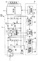
- FIG. 1 is a circuit diagram of a lighting fixture according to the first embodiment.
- This luminaire includes a light source lighting device 100.
- the light source lighting device 100 receives power from the AC power source 1 and turns on the light source 9.
- the light source 9 is not particularly limited, but is, for example, an LED (Light Emitting Diode).
- the light source lighting device 100 includes a power factor correction circuit 2, a DC-DC converter 3, a control unit 4, a gate drive unit 5, and a control power supply Vcc.
- the power factor correction circuit 2 includes a rectifier circuit DB.
- the rectifier circuit DB performs full-wave rectification of the AC power.
- This full-wave rectified voltage is not smoothed during the operation of the power factor correction circuit 2 but becomes a ripple voltage including twice the frequency of the AC power supply 1.
- the rectifier circuit DB rectifies AC power, and its output is connected to the high voltage line 20 and the low voltage line 22.
- the power factor correction circuit 2 is a boost chopper type.
- the power factor correction circuit 2 includes a filter capacitor C1, an inductor L1, a switching element SW, a diode D1, and a smoothing capacitor C2.
- the inductor L1 is provided on the high voltage line 20.
- the switching element SW includes a first terminal a, a second terminal b, and a control terminal c.
- the first terminal a is connected to the high voltage line 20 between the inductor L1 and the diode D1.
- the control terminal c is a terminal for conducting or blocking a current flowing from the first terminal a to the second terminal b.
- the first terminal a, the second terminal b, and the control terminal c can be a drain terminal, a source terminal, and a gate terminal, respectively.
- the anode of the diode D1 is connected to the inductor L1.
- the smoothing capacitor C2 connects the cathode of the diode D1 and the low voltage line 22.
- the power factor correction circuit 2 charges and discharges energy with the switching element SW and the inductor L1, and outputs a predetermined direct current voltage.
- the power factor correction circuit 2 includes a power supply voltage detection resistor R1 that detects a power supply voltage, a current detection resistor R2 that detects a current flowing through the switching element SW, and an output voltage detection resistor R3 that detects an output voltage.
- the current detection resistor R ⁇ b> 2 connects the second terminal b and the low voltage line 22.
- a DC-DC converter 3 for supplying a current to the light source 9 is connected to the output of the power factor correction circuit 2.
- the power factor correction circuit 2 operates under the control of the control unit 4.
- the power factor correction circuit 2 boosts the voltage that has been full-wave rectified by the rectifier circuit DB and performs DC smoothing. Further, the power factor improvement circuit 2 operates so that the input current waveform is sinusoidal and in phase with the voltage of the AC power source 1 under the control of the control unit 4 to improve the power factor.
- the control unit 4 includes a power supply voltage detection unit 4a, a current detection unit 4b, an output voltage detection unit 4c, and a gate signal generation unit 4d. You may comprise at least one part of the control part 4 with a microcomputer.
- the control unit 4 controls the switching element SW so that the output voltage, which is the voltage of the smoothing capacitor C2, becomes a preset voltage value while improving the power factor of the power factor correction circuit 2.
- the control unit 4 operates by obtaining driving power from the control power supply Vcc.
- the control power supply Vcc is obtained, for example, by converting the DC output of the rectifier circuit DB into a voltage suitable for the control unit 4 with a switching power supply or the like.
- the control power supply Vcc and the control unit 4 operate using the low voltage side of the rectifier circuit DB as a reference potential. In other words, the control power supply Vcc and the reference potential of the control unit 4 are set to the low voltage line 22.
- the power supply voltage detector 4a detects the full-wave rectified voltage divided by the power supply voltage detection resistor R1. The instantaneous value of the voltage in each power supply voltage phase can be detected by the power supply voltage detector 4a.
- the current detection unit 4b detects a current flowing from the inductor L1 to the switching element SW when the switching element SW is turned on by a voltage generated in the current detection resistor R2.
- the output voltage detection unit 4c detects the output voltage of the power factor correction circuit 2 as a voltage divided by the output voltage detection resistor R3.
- the output voltage detector 4c compares the target signal E1 corresponding to the target output voltage with the detected value of the output voltage, and outputs a signal corresponding to the difference between the two to the gate signal generator 4d.
- the gate signal generation unit 4d generates a gate signal for driving the switching element SW based on the detection signals respectively input from the power supply voltage detection unit 4a, the current detection unit 4b, and the output voltage detection unit 4c. 5 is output.
- This gate signal is, for example, a PWM (Pulse Width Modulation) signal.
- the output of the gate drive unit 5 is connected to the control terminal c and the second terminal b.
- the gate driver 5 amplifies the voltage of the gate signal output from the gate signal generator 4d to a voltage suitable for driving the switching element SW, and outputs the amplified voltage between the gate and source terminals of the switching element SW.
- a 5V gate signal output from the gate signal generation unit 4 d is amplified to 10 V by the gate driving unit 5.
- the switching element SW is turned on / off by a gate drive signal output from the gate driver 5.
- a gate resistor Rg may be connected to the control terminal c of the switching element SW.
- the DC-DC converter 3 is driven and controlled by a DC-DC converter control unit 6.
- the DC-DC converter 3 is subjected to constant current feedback control so that the current of the light source 9 becomes a target current value.
- the DC-DC converter 3 can be configured by a circuit such as a step-down chopper circuit or a flyback converter, for example.
- the rectifier circuit DB performs full-wave rectification on the input AC voltage, and the rectified voltage is applied to both ends of the filter capacitor C1.
- the filter capacitor C1 is provided for the purpose of removing the switching ripple, and is not for smoothing the frequency component of the AC power supply 1 here. Therefore, during the operation of the power factor correction circuit 2, the voltage across the filter capacitor C1 becomes a full-wave rectified voltage that pulsates in a sine wave at a frequency twice the AC power supply frequency.
- the switching element SW is turned on by a signal output from the gate driver 5.
- the full-wave rectified voltage is applied to the inductor L1, current flows through the path of the inductor L1, the switching element SW, and the current detection resistor R2, and energy is stored in the inductor L1.
- the current of the inductor L1 increases linearly.
- the current detection signal generated in the current detection resistor R2 increases. Then, when the current detection signal reaches a predetermined threshold voltage in the current detection unit 4b, the gate signal generation unit 4d outputs a gate signal for turning off the switching element SW. As a result, the switching element SW is turned off, the energy stored in the inductor L1 is released, and a current flows in the order of the inductor L1, the diode D1, and the smoothing capacitor C2. Thereby, the smoothing capacitor C2 is charged. At this time, the current of the inductor L1 decreases linearly. In this way, the energy is transmitted, and the DC-DC converter 3 supplies a current to the light source 9 with the voltage charged in the smoothing capacitor C2 as an input.
- the gate signal generation unit 4d When the switching element SW is turned off and a predetermined time elapses, the gate signal generation unit 4d outputs a gate signal for turning on the switching element SW again, and the gate driving unit 5 turns on the switching element SW.
- the current continuous mode is an operation mode in which the switching element SW is turned on before the current of the inductor L1 decreases and reaches zero, and the operation mode in which the switching element SW is turned on at the same time that the current of the inductor L1 reaches zero is current critical.
- the operation mode in which the switching element SW is turned on after a predetermined current zero period after the current of the inductor L1 reaches zero is referred to as a current discontinuous mode.
- the switching element SW can be operated in any one of these operation modes.
- the gate signal generation unit 4d controls the output voltage to the target voltage by controlling the ON time of the switching element SW based on the output voltage signal detected by the output voltage detection resistor R3 and the output voltage detection unit 4c. Furthermore, in order to make the envelope of the current peak value of the inductor L1 in each switching into a sine wave having the same phase as the power supply voltage, the threshold voltage of the current detection unit 4b is proportional to the power supply voltage signal detected by the power supply voltage detection unit 4a. And the OFF timing of the switching element SW in each switching is determined. As a result, the envelope of the inductor current peak value becomes a sinusoidal waveform while maintaining the output voltage at a desired voltage value.
- the filter capacitor C1 removes the switching ripple of the inductor current and averages it to make the input current close to a sine wave.
- the current detection resistor R2 is used to determine the timing for turning off the switching element SW described above, and in addition, an overcurrent that prevents an excessive current from flowing through the switching element SW and destroying the switching element SW when any abnormality occurs. It may also serve as a protective function.
- the circuit operation at the timing when the switching element SW is turned on while the power factor correction circuit 2 is operating will be described by taking the current continuous mode as an example.
- a current flows through the path of the inductor L1, the diode D1, and the smoothing capacitor C2, and a forward voltage is applied to the diode D1.
- the gate signal generation unit 4 d outputs a gate signal for turning on the switching element SW, and the gate driving unit 5 turns on the switching element SW.
- the predetermined time is determined by, for example, a preset driving frequency.
- the diode D1 is temporarily energized in the reverse direction due to the influence of accumulated carriers. Therefore, a reverse recovery current flows through the path of the smoothing capacitor C2, the diode D1, the switching element SW, and the current detection resistor R2.
- the reverse recovery current described above becomes a short-circuit current of the smoothing capacitor C2 at the moment when the switching element SW is turned on, and has a large peak value.
- the output of the gate drive unit 5 is connected to the GND which is the low-voltage side potential of the DC output of the rectifier circuit DB and the gate terminal of the switching element SW. Then, a gate drive voltage Vg based on GND is applied to the gate terminal as a gate drive signal for turning on the switching element SW.
- the reverse recovery current of the diode D1 flows through the current detection resistor R2 at the timing when the gate drive voltage is applied between the gate terminal and GND
- the voltage Ip ⁇ R2 across the current detection resistor R2 is superimposed on the gate drive voltage Vg. Therefore, the gate-source voltage Vgs applied between the gate terminal and the source terminal of the switching element SW becomes Vg ⁇ Ip ⁇ R2, and instantaneously decreases. That is, the voltage applied to the gate terminal decreases by Ip ⁇ R2.
- a switching element using GaN as a wide band gap semiconductor has characteristics that a gate threshold voltage is lower and a maximum rated voltage that can be applied between the gate and the source is lower than a conventional MOSFET using a silicon semiconductor. Therefore, the oscillating voltage generated by the influence of the reverse recovery current or the oscillating current may cause the switching element to be erroneously fired or broken.
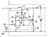
- FIG. 2 shows a circuit example of the gate drive unit 5 according to the first embodiment.
- the gate driver 5 includes transistors Tr1 and Tr2 and a transistor Tr3 connected in a totem pole shape.
- the gate signal from the gate signal generation unit 4d is input to the transistor Tr3.
- the gate driving unit 5 includes a diode Db that generates a gate driving power source Vb for generating a gate driving signal and a capacitor Cb.
- One end of the capacitor Cb is connected to the cathode side of the diode Db, and the other end is connected to a connection point between the second terminal b of the switching element SW and the current detection resistor R2.
- the anode side of the diode Db is connected to a control power supply Vcc that supplies power for operation of the control unit 4.
- the capacitor Cb has one end connected to the control power supply Vcc and the other end connected to the second terminal b.
- the control power supply Vcc and the control unit 4 use the low voltage side of the DC output of the rectifier circuit DB as a reference potential. Therefore, the gate signal generation unit 4d applies the gate signal to the gate drive unit 5 with the low voltage side of the DC output of the rectifier circuit DB as the reference potential.
- the gate drive power supply Vb is generated by charging the capacitor Cb through the path of the diode Db, the capacitor Cb, and the current detection resistor R2 from the control power supply Vcc. While the power factor correction circuit 2 is driven, the capacitor Cb is charged to the same voltage as the control power supply Vcc.
- the diode Db prevents discharge from the capacitor Cb to the control power supply Vcc when the sum of the voltages generated in the capacitor Cb and the current detection resistor R2 exceeds the voltage of the control power supply Vcc.
- a LOW signal of 0 V for example, is input from the gate signal generation unit 4d
- the transistor Tr3 is turned off, thereby turning on the transistor Tr1.
- a drive signal is applied to the switching element SW through the path of the capacitor Cb, the transistor Tr1, the gate resistance Rg, the control terminal c, the second terminal b, and the capacitor Cb, and the switching element SW is turned on.
- the transistor Tr3 When a 5V HIGH signal, for example, is input from the gate signal generation unit 4d, the transistor Tr3 is turned on, thereby turning on the transistor Tr2. As a result, the gate and source of the switching element SW are short-circuited by the transistor Tr2 via the gate resistance Rg in the path of the control terminal c, the gate resistance Rg, the transistor Tr2, and the second terminal b, and the switching element SW is turned off.
- the low voltage side of the capacitor Cb is connected to the connection point between the current detection resistor R2 and the second terminal b and is used as the reference potential of the gate driving power source Vb of the switching element SW, it is applied between the gate and drain terminals.
- the only voltage to be charged is the charging voltage of the capacitor Cb.
- a drive signal is applied from the capacitor Cb to the control terminal c. Therefore, a stable gate drive voltage can be applied between the gate and drain terminals of the switching element SW without depending on the voltage generated in the current detection resistor R2.
- the gate driving unit 5 according to the first embodiment can be said to receive the signal from the control unit 4 and drive the switching element SW by applying a voltage to the control terminal c using the potential of the second terminal b as a reference potential. .
- a circuit configuration different from that in FIG. 2 enabling this operation may be adopted.
- the reference potential of the control unit 4 is the low voltage side of the rectifier circuit DB as usual, the power supply voltage detection by the power supply voltage detection resistor R1, the current detection by the current detection resistor R2, and the output voltage detection by the output voltage detection resistor R3 are performed. It can be easily detected as a positive voltage with respect to the reference potential.
- the gate driving power source Vb can be generated from the conventional control power source Vcc, it is not necessary to provide a separate insulating power source or the like for gate driving.
- the peak current value of the reverse recovery current of the diode D1 is small.
- a Si fast recovery diode or a SiC Schottky barrier diode may be used as the diode D1.
- a peak inductance value of the reverse recovery current may be suppressed by adding a small inductance component in series to the path through which the reverse recovery current of the diode D1 flows.
- the gate drive voltage application method to the gate terminal of the switching element SW is not limited to the circuit method of FIG. 2, and other methods may be used.
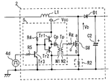
- a method of driving using a transformer Tp can be employed.
- the gate drive unit 5 shown in FIG. 3 includes a transformer Tp that receives power from the control power supply Vcc on the primary side and is connected to the control terminal c and the second terminal b on the secondary side and applies a drive signal to the control terminal c. I have.
- the transformer Tp includes a primary winding N1 and a secondary winding N2.
- the transformer Tp is, for example, a pulse transformer.
- one end of the secondary winding N2 of the transformer Tp is connected to the gate terminal side of the switching element SW, and the other end of the secondary winding N2 is connected to a connection point between the current detection resistor R2 and the second terminal b.
- the voltage applied between the gate and source terminals is only the voltage generated in the secondary winding N2 of the transformer Tp, and does not depend on the voltage generated in the current detection resistor R2. Therefore, a stable gate drive voltage can be applied between the gate and drain terminals of the switching element SW.
- the reference potential of the voltage applied to the gate terminal of the switching element SW in the power factor correction circuit 2 is not the reference potential of the control unit 4,
- the source terminal of the switching element SW was used. Therefore, even if the reverse recovery current of the diode D1 flows through the current detection resistor R2, the gate signal is not affected, and a phenomenon such as erroneous firing or destruction of the switching element SW can be suppressed.
- FIG. FIG. 4 is a circuit diagram of the light source lighting device 110 according to the second embodiment. The description of the same or corresponding configuration and operation as in the first embodiment is omitted.
- the light source lighting device 110 according to the second embodiment realizes the overcurrent protection operation of the switching element SW without using the current detection resistor R2 and the current detection unit 4b described in the first embodiment.
- the light source lighting device 110 includes an overcurrent detection winding L2 magnetically coupled to the inductor L1 and an overcurrent determination unit 4e provided to the control unit 4.
- the second terminal b of the switching element SW is connected to the low voltage line 22.
- FIG. 5 is a waveform diagram showing the power factor correction operation of the light source lighting device 110 according to the second embodiment.
- the switching element SW When the switching element SW is turned on, the current of the inductor L1 is proportional to E and is inversely proportional to the inductance of the inductor L1 when the instantaneous value of the full-wave rectified voltage is E [V]. That is, the current of the inductor L1 increases almost linearly in proportion to the on-time with the slope of E / L1.
- the peak value of the inductor L1 current in each switching is proportional to the voltage E of the instantaneous value of the full-wave rectified voltage.
- the envelope of the inductor L1 current is sinusoidal. Therefore, by removing the switching ripple of the inductor L1 current by the filter capacitor C1 and averaging it, the input current flowing from the AC power supply 1 can be brought close to a sine wave shape and can be substantially in phase with the AC power supply voltage. Therefore, power factor improvement and harmonic reduction can be achieved. Thus, it is not necessary to provide a current detection resistor for detecting the coil current at the source terminal of the switching element SW.
- the switching element SW may be destroyed. Therefore, even if a current detection resistor is not provided, the overcurrent is detected and the switching element SW is turned on. Need to turn off. Therefore, in the present embodiment, the overcurrent detection winding L2 magnetically coupled to the inductor L1 and the overcurrent determination unit 4e are provided in the control unit 4. When an excessive current flows through the switching element SW, this is detected by the overcurrent detection winding L2 and the overcurrent determination unit 4e, and the switching element SW is turned off. Thereby, destruction of the switching element SW is prevented.
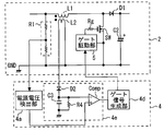
- FIG. 6 is a diagram illustrating a configuration example of the overcurrent determination unit 4e.
- the overcurrent determination unit 4e includes, for example, a voltage holding circuit including a diode D2, a capacitor C3, and a resistor R4, and a comparator Comp.
- This voltage holding circuit holds a voltage generated in the overcurrent detection winding L2 when the switching element SW is on.
- the voltage held by the voltage holding circuit is input to the negative input terminal of the comparator Comp.
- a voltage proportional to the instantaneous value of the full-wave rectified voltage is input from the power supply voltage detector 4a to the positive input terminal of the comparator Comp.
- the output signal of the comparator Comp is input to the gate signal generation unit 4d.
- the output of the gate signal generator 4d is provided to the gate driver 5 as a signal from the controller, and the gate driver 5 drives the switching element SW according to the signal.
- the overcurrent protection operation will be described.
- the full-wave rectified voltage rectified by the rectifier circuit DB is applied to the inductor L1.
- the overcurrent detection winding L2 a voltage determined by the voltage applied to the inductor L1 and the turn ratio of the number of turns of the inductor L1 and the number of turns of the overcurrent detection winding L2 is generated according to the principle of the transformer.
- the voltage generated in the overcurrent detection winding L2 is charged and held in the capacitor C3 via the diode D2.
- the voltage held by the capacitor C3 is input to the negative input terminal of the comparator Comp.
- a voltage proportional to the full-wave rectified voltage is input from the power supply voltage detector 4a to the positive input terminal of the comparator Comp.
- a voltage lower than the voltage generated in the overcurrent detection winding L2 is input to the positive input terminal of the comparator Comp.
- the voltages at the positive input terminal and the negative input terminal are compared by the comparator Comp.
- the comparator Comp outputs, for example, a LOW signal of 0V.
- the gate signal generation unit 4d that has received the LOW signal from the comparator Comp determines that the LOW signal is a normal signal, and continues the switching operation.
- the resistor R4 in FIG. 6 is for discharging the voltage of the capacitor C3 with an appropriate time constant. This is because, when the switching element SW is on, the voltage generated in the overcurrent detection winding L2 is proportional to the full-wave rectified voltage, so that a high voltage is not maintained, for example, near the zero cross where the full-wave rectified voltage is low. It is for making. That is, the resistance value of the resistor R4 is set so that the voltage of the capacitor C3 follows the instantaneous value in each phase of the full-wave rectified voltage while holding the voltage when the switching element SW is off.
- the winding of the inductor L1 and the overcurrent detection winding L2 are magnetically coupled to form a transformer.
- the magnetic flux does not increase any further, so that the magnetic flux does not change even if the current flowing through the inductor L1 changes. Therefore, in the overcurrent state, no voltage is induced in the overcurrent detection winding L2, or in the state close to magnetic saturation, the voltage induced in the overcurrent detection winding L2 decreases.
- the comparator Comp when the voltage of the overcurrent detection winding L2 generated when the switching element SW is turned on becomes lower than the voltage input to the comparator Comp from the power supply voltage detector 4a, the comparator Comp outputs a HIGH signal of 5V, for example. Upon receiving the HIGH signal, the gate signal generation unit 4d determines that the overcurrent state occurs, immediately turns off the switching element SW, and protects the switching element SW.
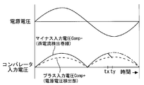
- FIG. 7 is a diagram showing a power supply voltage waveform, a voltage waveform at the negative input terminal of the comparator Comp, and a voltage waveform at the positive input terminal of the comparator Comp.
- the output of the comparator Comp is in a LOW state.
- the voltage Comp ⁇ at the minus input terminal of the comparator Comp falls below the voltage Comp + at the plus input terminal due to the magnetic saturation of the inductor L1
- the switching operation of the switching element SW is stopped.
- FIG. 7 shows that the voltage Comp ⁇ at the negative input terminal has decreased from time tx, and the voltage Comp ⁇ at the negative input terminal has fallen below the voltage Comp + at time ty.
- a voltage proportional to the full-wave rectified voltage is input from the power supply voltage detector 4a to the positive input terminal of the comparator Comp.
- the threshold voltage for determining the overcurrent state can be varied according to the power supply voltage phase, and the overcurrent state can be accurately determined in any power supply voltage phase.
- the difference between the voltage at the minus input terminal of the comparator Comp and the voltage at the plus input terminal can be set to be small in each phase. This enables rapid abnormal current detection in a state where the voltage is slightly lowered before the inductor L1 reaches the magnetic saturation state completely. That is, the overcurrent flowing through the switching element SW can be minimized, and damage to the switching element SW can be reduced.
- the control unit 4 includes the overcurrent detection winding L2 determined from the turn ratio between the number of turns of the winding constituting the inductor L1 and the number of turns of the overcurrent detection winding L2 in the conductive state of the switching element SW.
- the generated voltage generated in the overcurrent detection winding L2 is lower than the assumed generated voltage, the switching element SW is turned off.
- An example of “assumed generated voltage” is the output voltage of the power supply voltage detector 4a or a voltage slightly higher than the output voltage. In the above-described example, the voltage detected by the power supply voltage detector 4a that detects the output voltage of the rectifier circuit DB functions as the assumed generated voltage.
- An example of a circuit that provides “generated voltage” is a voltage holding circuit having the above-described diode D2, capacitor C3, and resistor R4.
- the power supply voltage detector 4a shifts the output voltage of the rectifier circuit DB to an assumed generated voltage, thereby reducing the assumed generated voltage slightly below the generated voltage when no overcurrent is generated as shown in FIG. Can be set.
- the overcurrent determination unit 4e in FIG. 6 has a simple circuit configuration shown for explaining the operation principle, and is not limited to this configuration, and may have another configuration.
- FIG. 8 is a diagram illustrating a configuration example of a light source lighting device that enables the current critical mode.
- the circuit of FIG. 8 is obtained by adding a zero current detection winding L3 provided magnetically coupled to the inductor L1 to the circuit of FIG.
- the control unit 4 can control the switching element SW in the current critical mode based on the voltage generated in the zero current detection winding L3.
- the light source lighting device of the second embodiment it is possible to perform power factor improvement and overcurrent protection operation without providing a current detection resistor at the source terminal of the switching element SW. Therefore, for example, a stable gate drive voltage can be applied between the gate and drain terminals of the switching element SW even when high-speed switching is performed using a wide band gap semiconductor such as GaN as the material of the switching element SW.
- FIG. 9 is a cross-sectional view of a lighting fixture 200 according to Embodiment 3.
- the lighting fixture 200 includes a lighting fixture body 40, a connector 41, a light source unit 42, a light source lighting device 43, and wirings 44 and 45.
- the luminaire main body 40 is a housing for attaching the light source lighting device 43 and the like.
- the connector 41 is a connection part for receiving power supply from an AC power source such as a commercial power source.
- the light source unit 42 is a substrate on which a light source such as an LED or an organic EL is mounted.
- the circuit configuration of the light source lighting device 43 can be the same circuit configuration as any one of the light source lighting devices described above.
- the light source lighting device 43 is supplied with power from an AC power source via the connector 41 and the wiring 44.
- the light source lighting device 43 converts the input power and supplies the converted power to the light source unit 42 via the wiring 45.
- the light source mounted on the light source unit 42 is turned on by the power supplied from the light source lighting device 43.
- the switching element SW A stable gate drive voltage can be applied between the gate and drain terminals.
- the material of the switching element SW can be silicon or a wide band gap semiconductor having a larger band gap than silicon.
- wide band gap semiconductors include silicon carbide, gallium nitride-based materials, and diamond.
- a wide band gap semiconductor is suitable for high-speed switching.
Landscapes
- Engineering & Computer Science (AREA)
- Power Engineering (AREA)
- Dc-Dc Converters (AREA)
- Circuit Arrangement For Electric Light Sources In General (AREA)
- Power Conversion In General (AREA)
- Rectifiers (AREA)
Abstract
交流電力を整流し出力が高圧線と低圧線に接続された整流回路と、該高圧線上に設けられたインダクタと、アノードが該インダクタに接続されたダイオードと、該ダイオードのカソードと該低圧線を接続する平滑コンデンサと、該インダクタと該ダイオードの間の該高圧線に接続された第1端子、第2端子、及び該第1端子から該第2端子の方向に流れる電流を導通または遮断する制御端子を有するスイッチング素子と、該第2端子と該低圧線を接続する電流検出抵抗と、を有する力率改善回路と、該スイッチング素子を制御する制御部と、該制御部からの信号を受け、該第2端子の電位を基準電位として該制御端子に電圧を印加して該スイッチング素子を駆動するゲート駆動部と、を備える。
Description
この発明は光源点灯装置と照明器具に関する。
例えば発光ダイオードなどの発光素子を点灯させるための各種の光源点灯装置が知られている。この種の光源点灯装置は、商用交流電源を整流及び平滑して直流電圧を生成するAC-DC変換回路と、得られた直流電圧から発光ダイオードに適した電流を供給するDC-DCコンバータを備える。多くの照明器具においては高力率が要求される。そのため、特許文献1に示すような、昇圧チョッパ形の力率改善回路がAC-DC変換回路として用いられている。
昇圧チョッパ形の力率改善回路は、スイッチング素子がオンし、コイル電流、すなわちスイッチング素子の電流が予め定められた値に達するとそれを検出してスイッチング素子がオフし、その後チョークコイルの電流が低下しコイル電流がゼロまたは有限の値まで低下すると次のスイッチングを開始するものである。これにより各スイッチング周期における、コイル電流のピーク値が正弦波状となるようにスイッチング素子のオン時間を制御し、力率を改善する。
ところで、このような光源点灯装置には、従来、Si半導体を用いた例えばMOSFETなどのスイッチング素子が用いられてきたが、近年はGaN又はSiCなどのワイドバンドギャップ半導体を用いたスイッチング素子が注目されている。ワイドバンドギャップ半導体を用いたスイッチング素子により高速なスイッチング動作が可能となり、例えば高周波駆動を行うことで光源点灯装置の小型化が期待できる。
力率改善回路では、コイル電流のピーク値を制御したり、コイル又はスイッチング素子に過大な電流が流れることを防止したりするため、スイッチング素子と直列に電流検出抵抗を設けることがある。電流検出抵抗よりスイッチング素子の電流を監視する。力率改善回路のスイッチング素子としてMOSFETを用いた場合、電流検出抵抗はMOSFETのソース端子と基準電位であるグラウンドとの間に接続される。
力率改善回路のスイッチング素子を高速スイッチングさせる場合、スイッチオン時に力率改善回路の出力側に設けられたダイオードのリカバリ特性により過大な逆回復電流がスイッチング素子に流れ込むという問題がある。この逆回復電流は電流検出抵抗にも流れるため、逆回復電流に応じて電流検出抵抗の両端には電位差が発生する。スイッチング素子を高速スイッチングするためには、GaNなどのワイドバンドギャップ半導体を用いることができる。例えばSiなどの別の材料を用いたスイッチング素子でも高速スイッチングする場合がある。
この電流検出抵抗の両端に発生した電位差はスイッチング素子のオンオフを制御するゲート端子と基準電位間に印加しているゲート信号電圧に重畳するため、スイッチング素子のゲート-ソース間に印加されるゲート-ソース間電圧Vgsが変動してしまう。さらに配線のインダクタンス成分又は浮遊容量成分によりゲート-ソース間に振動電圧を誘発する可能性がある。例えばワイドバンドギャップ半導体としてGaNを用いたスイッチング素子の場合、スイッチング素子のオン状態又はオフ状態を決定するゲートの閾値電圧が低く、且つ耐電圧も低い。そのため、ゲート-ソース間電圧Vgsの変動又は振動電圧の発生などにより、スイッチング素子の誤点弧又は破壊といった現象が発生する可能性がある。また、制御回路の基準電位をMOSFETのソース端子として、電流検出抵抗を基準電位-整流回路の低圧側間に接続した場合、ダイオードの逆回復電流の影響は受けないが、電流検出抵抗に発生する検出電圧が負電圧となってしまうため、制御回路が複雑化する問題がある。
本発明は上述の問題を解決するためになされたものであり、過電流検出を可能としつつ、スイッチング素子に対して良好なゲート駆動信号を与えることができる光源点灯装置と照明器具を提供することを目的とする。
本願の発明にかかる光源点灯装置は、交流電力を整流し出力が高圧線と低圧線に接続された整流回路と、該高圧線上に設けられたインダクタと、アノードが該インダクタに接続されたダイオードと、該ダイオードのカソードと該低圧線を接続する平滑コンデンサと、該インダクタと該ダイオードの間の該高圧線に接続された第1端子、第2端子、及び該第1端子から該第2端子の方向に流れる電流を導通または遮断する制御端子を有するスイッチング素子と、該第2端子と該低圧線を接続する電流検出抵抗と、を有する力率改善回路と、該スイッチング素子を制御する制御部と、該制御部からの信号を受け、該第2端子の電位を基準電位として該制御端子に電圧を印加して該スイッチング素子を駆動するゲート駆動部と、を備えたことを特徴とする。
本願の発明にかかる他の光源点灯装置は、交流電力を整流し出力が高圧線と低圧線に接続された整流回路と、該高圧線上に設けられたインダクタと、アノードが該インダクタに接続されたダイオードと、該ダイオードのカソードと該低圧線を接続する平滑コンデンサと、該インダクタと該ダイオードの間の該高圧線に接続された第1端子、該低圧線に接続された第2端子、及び該第1端子から該第2端子の方向に流れる電流を導通または遮断する制御端子を有するスイッチング素子と、を有する力率改善回路と、該スイッチング素子を制御する制御部と、該制御部からの信号を受け、該スイッチング素子を駆動するゲート駆動部と、該インダクタに磁気的に結合して設けられた過電流検出巻線と、を備え、該制御部は、該スイッチング素子の導通状態において、該インダクタを構成する巻線の巻数と該過電流検出巻線の巻き数との巻数比から決まる該過電流検出巻線の想定発生電圧よりも、該過電流検出巻線に発生した発生電圧が低い場合、該スイッチング素子をオフすることを特徴とする。
本発明のその他の特徴は以下に明らかにする。
この発明によれば、ソースと低圧線を電流検出抵抗で接続する場合はソースの電位を基準電位としてゲートに電圧を印加したり、そのような電流検出抵抗を省略してインダクタに磁気的に過電流検出巻線を結合したりすることで、過電流検出を可能としつつ、スイッチング素子に対して良好なゲート駆動信号を与えることができる。
実施の形態に係る光源点灯装置と照明器具について図面を参照して説明する。同じ又は対応する構成要素には同じ符号を付し、説明の繰り返しを省略する場合がある。
実施の形態1.
図1は、実施の形態1にかかる照明器具の回路図である。この照明器具は光源点灯装置100を含む。光源点灯装置100は交流電源1から電力の供給を受けて光源9を点灯させるものである。光源9は特に限定されないが例えばLED(Light Emitting Diode)である。光源点灯装置100は、力率改善回路2、DC-DCコンバータ3、制御部4、ゲート駆動部5及び制御電源Vccを備えている。力率改善回路2は整流回路DBを含んでいる。整流回路DBは交流電力を全波整流する。この全波整流電圧は、力率改善回路2の動作中は平滑されず、交流電源1の2倍の周波数を含むリプル電圧となる。整流回路DBは交流電力を整流し、その出力は高圧線20と低圧線22に接続されている。
図1は、実施の形態1にかかる照明器具の回路図である。この照明器具は光源点灯装置100を含む。光源点灯装置100は交流電源1から電力の供給を受けて光源9を点灯させるものである。光源9は特に限定されないが例えばLED(Light Emitting Diode)である。光源点灯装置100は、力率改善回路2、DC-DCコンバータ3、制御部4、ゲート駆動部5及び制御電源Vccを備えている。力率改善回路2は整流回路DBを含んでいる。整流回路DBは交流電力を全波整流する。この全波整流電圧は、力率改善回路2の動作中は平滑されず、交流電源1の2倍の周波数を含むリプル電圧となる。整流回路DBは交流電力を整流し、その出力は高圧線20と低圧線22に接続されている。
力率改善回路2は昇圧チョッパ型である。力率改善回路2は、フィルタコンデンサC1、インダクタL1、スイッチング素子SW、ダイオードD1、平滑コンデンサC2を備えている。インダクタL1は高圧線20上に設けられている。スイッチング素子SWは、第1端子a、第2端子b及び制御端子cを備えている。第1端子aは、インダクタL1とダイオードD1の間の高圧線20に接続されている。制御端子cは第1端子aから第2端子bの方向に流れる電流を導通または遮断するための端子である。第1端子a、第2端子b、制御端子cはそれぞれドレイン端子、ソース端子、ゲート端子とすることができる。
ダイオードD1のアノードはインダクタL1に接続されている。平滑コンデンサC2はダイオードD1のカソードと低圧線22を接続している。力率改善回路2は、DC-DCコンバータ3を介して光源9に直流電流を供給するために、スイッチング素子SWとインダクタL1でエネルギの充放電を行い、予め定められた直流電圧を出力する。
また、力率改善回路2は、電源電圧を検出する電源電圧検出抵抗R1、スイッチング素子SWに流れる電流を検出する電流検出抵抗R2及び出力電圧を検出する出力電圧検出抵抗R3を備えている。電流検出抵抗R2は第2端子bと低圧線22を接続している。力率改善回路2の出力には、光源9に電流を供給するためのDC-DCコンバータ3が接続されている。
力率改善回路2は制御部4の制御を受けて動作する。力率改善回路2は、整流回路DBが全波整流した電圧を昇圧して直流平滑する。さらに、力率改善回路2は制御部4の制御により入力電流波形を正弦波状で且つ交流電源1の電圧と同位相となるように動作し、力率改善を行う。
制御部4は、電源電圧検出部4a、電流検出部4b、出力電圧検出部4c及びゲート信号生成部4dを備えている。制御部4の少なくとも一部をマイクロコンピュータで構成してもよい。制御部4は、力率改善回路2の力率を改善しつつ、平滑コンデンサC2の電圧である出力電圧が予め設定された電圧値となるように、スイッチング素子SWを制御する。また、制御部4は制御電源Vccより駆動用の電力を得て動作する。制御電源Vccは、例えば、整流回路DBの直流出力をスイッチング電源等で制御部4に適した電圧に変換して得る。制御電源Vcc及び制御部4は整流回路DBの低圧側を基準電位として動作する。言いかえれば、制御電源Vcc及び制御部4の基準電位は、低圧線22に設定されている。
電源電圧検出部4aは電源電圧検出抵抗R1により分圧した全波整流電圧を検出する。電源電圧検出部4aによって各電源電圧位相における電圧の瞬時値を検知することができる。電流検出部4bは、スイッチング素子SWがオンの時に、インダクタL1からスイッチング素子SWにかけて流れる電流を電流検出抵抗R2に発生する電圧によって検出するものである。出力電圧検出部4cは、力率改善回路2の出力電圧を出力電圧検出抵抗R3によって分圧した電圧として検出するものである。出力電圧検出部4cでは、目標出力電圧に相当する目標信号E1と出力電圧の検出値を比較し、両者の差に応じた信号をゲート信号生成部4dに出力する。ゲート信号生成部4dは、電源電圧検出部4a、電流検出部4b及び出力電圧検出部4cからそれぞれ入力された検出信号に基づいてスイッチング素子SWを駆動するためのゲート信号を生成し、ゲート駆動部5に出力する。このゲート信号は例えばPWM(Pulse Width Modulation)信号である。
ゲート駆動部5の出力は制御端子cと第2端子bに接続されている。ゲート駆動部5は、ゲート信号生成部4dから出力されたゲート信号の電圧をスイッチング素子SWの駆動に適した電圧に増幅してスイッチング素子SWのゲート-ソース端子間に出力する。例えば、ゲート信号生成部4dから出力された5Vのゲート信号が、ゲート駆動部5で10Vに増幅される。スイッチング素子SWはゲート駆動部5から出力されたゲート駆動信号によりオンオフ動作を行う。なお、スイッチング素子SWの制御端子cにはゲート抵抗Rgを接続してもよい。
DC-DCコンバータ3は、DC-DCコンバータ制御部6により駆動及び制御される。DC-DCコンバータ3は、光源9の電流が目標電流値となるように定電流フィードバック制御される。なお、DC-DCコンバータ3は、例えば降圧チョッパ回路又はフライバックコンバータなどの回路で構成することができる。
次に、実施の形態1にかかる光源点灯装置100の動作を説明する。光源点灯装置100に交流電源1が印加されると、整流回路DBは入力された交流電圧を全波整流し、整流された電圧がフィルタコンデンサC1の両端に印加される。フィルタコンデンサC1は、スイッチングリプルを除去する目的で設けられたものであり、ここでは交流電源1の周波数成分を平滑するためのものではない。したがって、力率改善回路2の動作中は、フィルタコンデンサC1の両端電圧は、交流電源周波数の2倍周波数で正弦波状に脈動する全波整流電圧となる。
定常動作状態における力率改善回路2の動作を説明する。まず、ゲート駆動部5から出力される信号により、スイッチング素子SWがオンしている状態とする。スイッチング素子SWがオンすると、全波整流電圧はインダクタL1に印加され、インダクタL1、スイッチング素子SW、電流検出抵抗R2の経路で電流が流れ、インダクタL1にエネルギが蓄えられる。このとき、インダクタL1の電流は直線的に増加していく。
インダクタL1の電流増加に伴って、電流検出抵抗R2に発生する電流検出信号も増加する。そして、電流検出部4bにて電流検出信号が予め定められた閾値電圧に達するとゲート信号生成部4dはスイッチング素子SWをオフするゲート信号を出力する。これによりスイッチング素子SWはオフし、インダクタL1に蓄えられたエネルギが放出され、インダクタL1、ダイオードD1、平滑コンデンサC2の順に電流が流れる。これにより、平滑コンデンサC2を充電する。このとき、インダクタL1の電流は直線的に減少していく。このようにエネルギを伝達し、DC-DCコンバータ3は平滑コンデンサC2に充電された電圧を入力として、光源9に電流を供給する。
スイッチング素子SWがオフして予め定められた時間が経過すると、ゲート信号生成部4dは再びスイッチング素子SWをオンするゲート信号を出力し、ゲート駆動部5はスイッチング素子SWをオンする。なお、インダクタL1の電流が減少し、ゼロに到達する前にスイッチング素子SWがオンする動作モードを電流連続モード、インダクタL1の電流がゼロに到達すると同時にスイッチング素子SWがオンする動作モードを電流臨界モード、インダクタL1の電流がゼロに到達後予め定められた電流ゼロ期間を経てスイッチング素子SWがオンする動作モードを電流不連続モードという。本実施の形態においては、これらの何れか1つの動作モードでスイッチング素子SWを動作させることができる。
ゲート信号生成部4dは出力電圧検出抵抗R3及び出力電圧検出部4cで検出した出力電圧信号に基づいてスイッチング素子SWのオン時間を制御することで出力電圧を目標電圧に制御する。さらに、各スイッチングにおけるインダクタL1の電流ピーク値の包絡線を電源電圧と同位相の正弦波状とするため、電源電圧検出部4aにより検出した電源電圧信号に比例するように電流検出部4bの閾値電圧を決定し、各スイッチングにおけるスイッチング素子SWのオフタイミングを決定する。これにより出力電圧を所望の電圧値に保ちながら、インダクタ電流ピーク値の包絡線が正弦波状の波形となるようにする。そして、フィルタコンデンサC1によりインダクタ電流のスイッチングリプルを取り除き平均化することで、入力電流を正弦波状に近づける。なお、必要に応じて整流回路DBの交流入力側にノイズ抑制のためフィルタ回路を追加してもよい。また、電流検出抵抗R2は、上述したスイッチング素子SWをオフするタイミングの決定に用いることに加えて、何らかの異常時にスイッチング素子SWに過大な電流が流れスイッチング素子SWが破壊することを防止する過電流保護機能を兼ねても良い。
ここで、力率改善回路2が動作中において、スイッチング素子SWがオンするタイミングにおける回路動作について、電流連続モードを例として説明する。まず、スイッチング素子SWがオフ状態とすると、インダクタL1、ダイオードD1、平滑コンデンサC2の経路で電流が流れ、ダイオードD1には順方向電圧が印加されている状態となる。
次いで、予め定められた時間が経過すると、ゲート信号生成部4dはスイッチング素子SWをオンするゲート信号を出力し、ゲート駆動部5によりスイッチング素子SWがオンする。予め定められた時間は、例えば、予め設定しておいた駆動周波数などによって決まる。スイッチング素子SWがオンした瞬間にダイオードD1のアノード側と平滑コンデンサC2の低圧側がスイッチング素子SWと電流検出抵抗R2を介して導通状態となるため、ダイオードD1には平滑コンデンサC2の電圧が逆方向電圧として印加することとなる。
この時、ダイオードD1のリカバリ特性により、ダイオードD1は蓄積キャリアの影響で一時的に逆方向に通電が可能な状態となる。そのため、平滑コンデンサC2、ダイオードD1、スイッチング素子SW、電流検出抵抗R2の経路で逆回復電流が流れる。例えばGaN等のワイドバンドギャップ半導体を用いたスイッチング素子SWにおいてはスイッチング速度が非常に高速であり、且つ電流検出抵抗R2は損失低減のため一般的に低抵抗である。そのため上述の逆回復電流は、スイッチング素子SWがオンした瞬間はほぼ平滑コンデンサC2の短絡電流となり、ピーク値の大きな電流となる。この逆回復電流が電流検出抵抗R2に流れると、電流検出抵抗R2の両端には電流値に応じた電圧降下が発生する。すなわち、逆回復電流のピーク値をIp、電流検出抵抗R2の抵抗値をR2とすると、Ip×R2の電圧が電流検出抵抗R2の両端に発生する。
ここで、仮に、ゲート駆動部5の出力がスイッチング素子SWのゲート端子と整流回路DBの直流出力の低圧側の電位であるGNDに接続されているとする。すると、スイッチング素子SWをオンするゲート駆動信号として、GNDを基準としたゲート駆動電圧Vgがゲート端子に印加される。そして、ゲート端子とGND間にゲート駆動電圧が印加されたタイミングで電流検出抵抗R2にダイオードD1の逆回復電流が流れると、ゲート駆動電圧Vgに電流検出抵抗R2の両端電圧Ip×R2が重畳するため、スイッチング素子SWのゲート端子とソース端子の間に印加されるゲート-ソース間電圧VgsはVg-Ip×R2となり、瞬間的に低下する。つまり、ゲート端子に印加される電圧がIp×R2だけ低下する。
さらには、逆回復電流がゼロになった後も、逆回復電流が流れた電流経路に存在する寄生インダクタンスと浮遊容量の影響による振動電流が電流検出抵抗R2に流れる。この振動電流は電圧変換されて、ゲート駆動電圧Vgに重畳する。これにより、スイッチング素子SWがオンするタイミングにおいて、ゲート-ソース間電圧Vgsに過大な振動が発生する可能性がある。
例えば、ワイドバンドギャップ半導体としてGaNを用いたスイッチング素子は従来のシリコン半導体を用いたMOSFETと比較すると、ゲート閾値電圧が低く、且つゲート-ソース間に印加できる最大定格電圧も低いという特性がある。したがって、逆回復電流又は振動電流の影響により発生する振動電圧で、スイッチング素子の誤点弧又は破壊を引き起こす可能性がある。
図2は、実施の形態1に係るゲート駆動部5の回路例を示すである。ゲート駆動部5はトーテムポール形に接続されたトランジスタTr1、Tr2と、トランジスタTr3を有している。トランジスタTr3には、ゲート信号生成部4dからのゲート信号が入力される。そして、ゲート駆動部5は、ゲート駆動信号を生成するためのゲート駆動用電源Vbを生成するダイオードDbとコンデンサCbを備える。コンデンサCbは一端がダイオードDbのカソード側に接続され、他端はスイッチング素子SWの第2端子bと電流検出抵抗R2の接続点に接続される。ダイオードDbのアノード側は制御部4の動作用の電源を供給する制御電源Vccに接続される。そのため、コンデンサCbは一端が制御電源Vccに接続され他端が第2端子bに接続されたということができる。制御電源Vcc及び制御部4は整流回路DBの直流出力の低圧側を基準電位としている。したがって、ゲート信号生成部4dは整流回路DBの直流出力の低圧側を基準電位として、ゲート駆動部5にゲート信号を印加する。
ゲート駆動用電源Vbは、制御電源VccよりダイオードDb、コンデンサCb、電流検出抵抗R2の経路でコンデンサCbを充電することで生成する。力率改善回路2が駆動中、コンデンサCbは制御電源Vccとほぼ同じ電圧まで充電された状態となる。ダイオードDbは、コンデンサCbと電流検出抵抗R2に発生する電圧の合計が制御電源Vccの電圧を超えた場合に、コンデンサCbから制御電源Vccへの放電を防止するものである。ゲート信号生成部4dから例えば0VのLOW信号が入力されると、トランジスタTr3はオフ状態となり、これによりトランジスタTr1がオンする。すると、コンデンサCb、トランジスタTr1、ゲート抵抗Rg、制御端子c、第2端子b、コンデンサCbの経路でスイッチング素子SWに駆動信号が印加され、スイッチング素子SWはオンする。
ゲート信号生成部4dから例えば5VのHIGH信号が入力されると、トランジスタTr3はオン状態となり、これによりトランジスタTr2がオンする。これにより制御端子c、ゲート抵抗Rg、トランジスタTr2、第2端子bの経路でスイッチング素子SWのゲート-ソース間がゲート抵抗Rgを介してトランジスタTr2により短絡されて、スイッチング素子SWはオフする。
このように、電流検出抵抗R2と第2端子bの接続点にコンデンサCbの低圧側を接続し、スイッチング素子SWのゲート駆動用電源Vbの基準電位としたので、ゲート-ドレイン端子間に印加される電圧は、コンデンサCbの充電電圧のみとなる。このコンデンサCbから制御端子cに駆動信号を印加する。したがって、電流検出抵抗R2に発生する電圧に依存せず、スイッチング素子SWのゲート-ドレイン端子間に安定したゲート駆動電圧を印加することができる。実施の形態1に係るゲート駆動部5は、制御部4からの信号を受け、第2端子bの電位を基準電位として制御端子cに電圧を印加してスイッチング素子SWを駆動するということができる。この動作を可能とする図2とは異なる回路構成を採用してもよい。
また、制御部4の基準電位は従来通り、整流回路DBの低圧側としているので、電源電圧検出抵抗R1による電源電圧検出、電流検出抵抗R2による電流検出及び出力電圧検出抵抗R3による出力電圧検出は、基準電位に対して正電圧として容易に検出することができる。また、ゲート駆動用電源Vbも従来の制御電源Vccから生成できるため、ゲート駆動用に別途絶縁電源等を設ける必要はない。
ダイオードD1の逆回復電流のピーク電流値は小さい方が望ましい。ダイオードD1の逆回復電流のピーク電流値を抑制するため、ダイオードD1として、例えばSiファストリカバリダイオード又はSiCショットキーバリアダイオードなどを用いてもよい。また、ダイオードD1の逆回復電流が流れる経路に直列に小さなインダクタンス成分を追加して、逆回復電流のピーク電流値を抑制してもよい。
スイッチング素子SWのゲート端子へのゲート駆動電圧印加方法は図2の回路方式に限定するものではなく、他の方法でも良い。例えば、図3に示すように、トランスTpを用いて駆動する方法を採用することができる。図3に示すゲート駆動部5は、一次側で制御電源Vccから電力供給を受け、二次側で制御端子cと第2端子bに接続されて制御端子cに駆動信号を印加するトランスTpを備えている。トランスTpは一次巻線N1と二次巻線N2を備えている。トランスTpは例えばパルストランスである。本方式ではトランスTpの二次巻線N2の一端をスイッチング素子SWのゲート端子側に接続し、二次巻線N2の他端を電流検出抵抗R2と第2端子bとの接続点に接続した。これにより、ゲート-ソース端子間に印加される電圧はトランスTpの二次巻線N2に発生する電圧のみとなり、電流検出抵抗R2に発生する電圧に依存しない。したがってスイッチング素子SWのゲート-ドレイン端子間に安定したゲート駆動電圧を印加することができる。
このように、実施の形態1に係る光源点灯装置と照明器具によれば、力率改善回路2におけるスイッチング素子SWのゲート端子に印加する電圧の基準電位を、制御部4の基準電位ではなく、スイッチング素子SWのソース端子とした。これにより、電流検出抵抗R2にダイオードD1の逆回復電流が流れてもゲート信号に影響を与えず、スイッチング素子SWの誤点弧又は破壊といった現象を抑制することができる。
実施の形態2.
図4は、実施の形態2にかかる光源点灯装置110の回路図である。実施の形態1と同一又は対応する構成及び動作ついては説明を省略する。実施の形態2に係る光源点灯装置110は、実施の形態1で説明した電流検出抵抗R2と電流検出部4bを使用せず、スイッチング素子SWの過電流保護動作を実現するものである。光源点灯装置110は、インダクタL1に磁気的に結合した過電流検出巻線L2と、制御部4に提供された過電流判定部4eを備える。スイッチング素子SWの第2端子bは低圧線22に接続されている。
図4は、実施の形態2にかかる光源点灯装置110の回路図である。実施の形態1と同一又は対応する構成及び動作ついては説明を省略する。実施の形態2に係る光源点灯装置110は、実施の形態1で説明した電流検出抵抗R2と電流検出部4bを使用せず、スイッチング素子SWの過電流保護動作を実現するものである。光源点灯装置110は、インダクタL1に磁気的に結合した過電流検出巻線L2と、制御部4に提供された過電流判定部4eを備える。スイッチング素子SWの第2端子bは低圧線22に接続されている。
次に、光源点灯装置110の動作を、電流不連続モードを例に説明する。図5は実施の形態2にかかる光源点灯装置110の力率改善動作を示す波形図である。スイッチング素子SWをオンすると、インダクタL1の電流は、全波整流電圧の瞬時値の電圧をE[V]とすると、Eに比例し、インダクタL1のインダクタンスに反比例する。すなわち、インダクタL1の電流はE/L1の傾きでオン時間に比例してほぼ直線的に増加していく。
次に、予め定められたオン時間t(ON)が経過するとスイッチング素子SWはオフする。すると、インダクタL1の電流は、力率改善回路の出力電圧をVo[V]とすると、-(Vo-E)/L1の傾きで直線的に減少していく。そして、インダクタL1の電流がゼロに到達後、再びスイッチング素子SWがオンする動作を繰り返す。
そして、電源半周期間におけるスイッチング素子SWのオン時間t(ON)をすべて同一時間に設定すれば、各スイッチングにおけるインダクタL1電流のピーク値は全波整流電圧の瞬時値の電圧Eに比例するため、インダクタL1電流の包絡線は正弦波状となる。よって、フィルタコンデンサC1によりインダクタL1電流のスイッチングリプルを取り除き平均化することで、交流電源1から流れ込む入力電流を正弦波状に近づけるとともに交流電源電圧とほぼ同位相にすることができる。よって、力率改善及び高調波低減ができる。これより、コイル電流を検出するための電流検出抵抗をスイッチング素子SWのソース端子に設ける必要がない。
しかしながら、何らかの理由により、スイッチング素子SWに過大な電流が流れた場合スイッチング素子SWが破壊する可能性があるため、電流検出抵抗が設けられていない場合でも、過電流を検知してスイッチング素子SWをオフする必要がある。そこで、本実施の形態では、インダクタL1に磁気的に結合した過電流検出巻線L2と、制御部4に過電流判定部4eを設けた。スイッチング素子SWに過大な電流が流れた場合、過電流検出巻線L2と過電流判定部4eによってこれを検出してスイッチング素子SWをオフする。これによりスイッチング素子SWの破壊が防止される。
図6は、過電流判定部4eの構成例を示す図である。過電流判定部4eは、例えばダイオードD2、コンデンサC3及び抵抗R4を備えた電圧保持回路と、コンパレータCompとを有する。この電圧保持回路はスイッチング素子SWがオンの時に過電流検出巻線L2に発生する電圧を保持するものである。電圧保持回路で保持された電圧はコンパレータCompのマイナス入力端子に入力される。コンパレータCompのプラス入力端子には、電源電圧検出部4aより全波整流電圧の瞬時値に比例した電圧が入力される。コンパレータCompの出力信号はゲート信号生成部4dに入力される。ゲート信号生成部4dの出力が制御部からの信号としてゲート駆動部5に提供され、その信号に従ってゲート駆動部5がスイッチング素子SWを駆動する。
次に、過電流保護動作について説明する。正常動作時は、スイッチング素子SWがオンすると、インダクタL1には整流回路DBで整流された全波整流電圧が印加される。そして、過電流検出巻線L2には、トランスの原理により、インダクタL1に印加された電圧と、インダクタL1の巻数と過電流検出巻線L2の巻数の巻数比で決まる電圧が発生する。過電流検出巻線L2に発生した電圧はダイオードD2を介してコンデンサC3に充電されて、保持される。コンデンサC3により保持された電圧は、コンパレータCompのマイナス入力端子に入力される。
一方、コンパレータCompのプラス入力端子には、全波整流電圧に比例した電圧が電源電圧検出部4aより入力される。正常動作時は、コンパレータCompのプラス入力端子に、過電流検出巻線L2に発生する電圧よりも低い電圧が入力されるものとする。プラス入力端子とマイナス入力端子の電圧がコンパレータCompで比較されるが、ここでは、過電流検出巻線L2に発生する電圧の方が高いため、コンパレータCompは例えば0VのLOW信号を出力する。コンパレータCompよりLOW信号を受け取ったゲート信号生成部4dはLOW信号を正常信号と判断し、引き続きスイッチング動作を継続させる。
なお、スイッチング素子SWがオフした場合は、インダクタL1に蓄えられたエネルギが放出される動作となるため、スイッチング素子SWがオンの時とは逆方向の電圧がインダクタL1に発生する。それに伴い、過電流検出巻線L2に発生する電圧も極性が反転する。そこで、ダイオードD2の整流動作により、コンパレータCompのマイナス入力端子に逆電圧が印加されることを阻止し、スイッチング素子SWがオフの時も引き続きコンデンサC3に充電されるようにした。こうして、スイッチング素子SWがオフ時に過電流検出巻線L2に発生した電圧をコンパレータCompのマイナス入力端子に入力する。
図6における抵抗R4は、コンデンサC3の電圧を適当な時定数で放電するためのものである。これは、スイッチング素子SWがオン時に、過電流検出巻線L2に発生する電圧が全波整流電圧に比例するため、例えば全波整流電圧が低くなるゼロクロス付近のときに、高い電圧が保持されないようにするためのものである。すなわち、コンデンサC3の電圧が、スイッチング素子SWがオフ時は電圧を保持しつつ、全波整流電圧の各位相における瞬時値に追従するように抵抗R4の抵抗値を設定する。
次に、異常動作時の動作について説明する。何らかの理由により、スイッチング素子SWに過電流が流れた場合を想定する。スイッチング素子SWがオンしている時は、インダクタL1とスイッチング素子SWが直列接続となっているため、電源より供給された過電流はインダクタL1にも同時に流れている状態となる。過電流状態においては、インダクタL1の磁路を形成している磁性体の磁束密度は飽和状態に至っているものとする。
インダクタL1の巻線と過電流検出巻線L2は磁気的に結合していることからトランスを形成している。しかし、インダクタL1に流れる電流により磁路を形成する磁性体が飽和状態にある場合、それ以上磁束が増えないため、インダクタL1に流れる電流が変化しても磁束の変化が生じない。したがって、過電流状態においては、過電流検出巻線L2には電圧が誘起されないか、磁気飽和に近い状態では過電流検出巻線L2に誘起される電圧が低下する。
そこで、スイッチング素子SWがオン時に発生する過電流検出巻線L2の電圧が、電源電圧検出部4aよりコンパレータCompに入力される電圧よりも低くなると、コンパレータCompは例えば5VのHIGH信号を出力する。HIGH信号を受けたゲート信号生成部4dは過電流状態と判断し、直ちにスイッチング素子SWをオフし、スイッチング素子SWを保護する。
図7は、電源電圧波形と、コンパレータCompのマイナス入力端子の電圧波形と、コンパレータCompのプラス入力端子の電圧波形を示す図である。マイナス入力端子の電圧Comp-が、プラス入力端子の電圧Comp+を上回っている場合、コンパレータCompの出力はLOW状態となる。他方、コンパレータCompのマイナス入力端子の電圧Comp-が、インダクタL1の磁気飽和により、プラス入力端子の電圧Comp+を下回ると過電流状態と判断してコンパレータCompの出力はHIGH状態となる。よって、スイッチング素子SWのスイッチング動作が停止する。図7では、時刻txからマイナス入力端子の電圧Comp-が低下し、時刻tyにおいてマイナス入力端子の電圧Comp-が電圧Comp+を下回ったことが図示されている。
コンパレータCompのプラス入力端子には、全波整流電圧に比例した電圧が電源電圧検出部4aより入力される。これにより、電源電圧位相に応じて過電流状態と判定する閾値電圧を変動させ、何れの電源電圧位相においても正確に過電流状態を判別することができる。また、コンパレータCompのマイナス入力端子の電圧と、プラス入力端子の電圧の差を、各位相において、それぞれ小さく設定することができる。これは、インダクタL1が完全に磁気飽和状態に至る前の若干電圧が下がった状態での迅速な異常電流検知を可能とする。すなわち、スイッチング素子SWに流れる過電流を最小限に留めることができ、スイッチング素子SWのダメージを軽減できる。
実施の形態2に係る制御部4は、スイッチング素子SWの導通状態において、インダクタL1を構成する巻線の巻数と過電流検出巻線L2の巻数との巻数比から決まる過電流検出巻線L2の想定発生電圧よりも、過電流検出巻線L2に発生した発生電圧が低い場合、スイッチング素子SWをオフする。「想定発生電圧」の例が電源電圧検出部4aの出力電圧又はその出力電圧より若干高い電圧である。上述の例では、整流回路DBの出力電圧を検出する電源電圧検出部4aで検出された電圧が想定発生電圧として機能する。「発生電圧」を提供する回路例は、前述のダイオードD2、コンデンサC3及び抵抗R4を有する電圧保持回路である。電源電圧検出部4aは整流回路DBの出力電圧をレベルシフトして想定発生電圧とすることで、図7に示すように過電流が発生していないときの発生電圧を僅かに下回る想定発生電圧を設定することができる。また、図6の過電流判定部4eは動作原理を説明するために示した簡略的な回路構成であり、この構成に限定されるものではなく、他の構成でも構わない。
ここではスイッチング素子SWの過電流保護動作について、力率改善回路2を電流不連続モードで動作させた場合について説明した。しかしながら、電流臨界モード又は電流連続モードを採用する場合でも、同様に過電流保護動作を行うことができる。図8は、電流臨界モードを可能とする光源点灯装置の構成例を示す図である。図8の回路は、図4の回路に、インダクタL1に磁気的に結合して設けられたゼロ電流検出巻線L3を付加したものである。制御部4は、ゼロ電流検出巻線L3で生じた電圧に基づいて電流臨界モードでスイッチング素子SWを制御することができる。
実施の形態2の光源点灯装置によれば、スイッチング素子SWのソース端子に電流検出抵抗を設けずに力率改善と過電流保護動作を行うことができる。そのため、例えば、スイッチング素子SWの材料としてGaNなどのワイドバンドギャップ半導体を用いて、高速スイッチングを行っても、スイッチング素子SWのゲート-ドレイン端子間に安定したゲート駆動電圧を印加することができる。
実施の形態3.
図9は、実施の形態3に係る照明器具200の断面図である。照明器具200は、照明器具本体40、コネクタ41、光源ユニット42、光源点灯装置43及び配線44、45を備えている。照明器具本体40は、光源点灯装置43などを取り付けるための筺体である。コネクタ41は、商用電源などの交流電源から電力の供給を受けるための接続部である。光源ユニット42は、LED又は有機ELなどの光源を実装した基板である。
図9は、実施の形態3に係る照明器具200の断面図である。照明器具200は、照明器具本体40、コネクタ41、光源ユニット42、光源点灯装置43及び配線44、45を備えている。照明器具本体40は、光源点灯装置43などを取り付けるための筺体である。コネクタ41は、商用電源などの交流電源から電力の供給を受けるための接続部である。光源ユニット42は、LED又は有機ELなどの光源を実装した基板である。
光源点灯装置43の回路構成は、上述した光源点灯装置のいずれか1つと同じ回路構成とすることができる。光源点灯装置43は、コネクタ41と配線44を介して交流電源からの電力供給を受ける。光源点灯装置43は、入力した電力を変換し、変換された電力を配線45を介して光源ユニット42に供給する。光源点灯装置43から供給された電力により、光源ユニット42に実装された光源が点灯する。これにより、上述した実施形態にかかる光源点灯装置の利点を備えた照明器具200が提供される。
照明器具200によれば、実施の形態1又は2で述べた光源点灯装置を備えることで、例えばGaNなどのワイドバンドギャップ半導体を用いたスイッチング素子SWで高速スイッチングを行っても、スイッチング素子SWのゲート-ドレイン端子間に安定したゲート駆動電圧を印加することができる。
ここまでに説明した変形例は、その変形例が記載された実施の形態以外の実施の形態にも応用できる。また、すべての実施形態において、スイッチング素子SWの材料は珪素又は珪素に比べてバンドギャップが大きいワイドバンドギャップ半導体とすることができる。ワイドバンドギャップ半導体として、例えば、炭化珪素、窒化ガリウム系材料又はダイヤモンドがある。ワイドバンドギャップ半導体は高速スイッチングに好適である。
1 交流電源、 2 力率改善回路、 3 DC-DCコンバータ、 4 制御部、 5 ゲート駆動部、 9 光源、 43 光源点灯装置、 100 光源点灯装置、 110 光源点灯装置、 200 照明器具
Claims (11)
- 交流電力を整流し出力が高圧線と低圧線に接続された整流回路と、
前記高圧線上に設けられたインダクタと、
アノードが前記インダクタに接続されたダイオードと、
前記ダイオードのカソードと前記低圧線を接続する平滑コンデンサと、
前記インダクタと前記ダイオードの間の前記高圧線に接続された第1端子、第2端子、及び前記第1端子から前記第2端子の方向に流れる電流を導通または遮断する制御端子を有するスイッチング素子と、
前記第2端子と前記低圧線を接続する電流検出抵抗と、を有する力率改善回路と、
前記スイッチング素子を制御する制御部と、
前記制御部からの信号を受け、前記第2端子の電位を基準電位として前記制御端子に電圧を印加して前記スイッチング素子を駆動するゲート駆動部と、を備えたことを特徴とする光源点灯装置。 - 前記制御部の動作用の電源を供給する制御電源を備え、
前記ゲート駆動部は、一端が前記制御電源に接続され他端が前記第2端子に接続されたコンデンサを備え、前記コンデンサから前記制御端子に駆動信号を印加することを特徴とする請求項1に記載の光源点灯装置。 - 前記制御部の動作用の電源を供給する制御電源を備え、
前記ゲート駆動部は、一次側で前記制御電源から電力供給を受け、二次側で前記制御端子と前記第2端子に接続されて前記制御端子に駆動信号を印加するトランスを備えたことを特徴とする請求項1に記載の光源点灯装置。 - 前記制御電源及び前記制御部の基準電位は、前記低圧線に設定されたことを特徴とする請求項2又は3に記載の光源点灯装置。
- 交流電力を整流し出力が高圧線と低圧線に接続された整流回路と、
前記高圧線上に設けられたインダクタと、
アノードが前記インダクタに接続されたダイオードと、
前記ダイオードのカソードと前記低圧線を接続する平滑コンデンサと、
前記インダクタと前記ダイオードの間の前記高圧線に接続された第1端子、前記低圧線に接続された第2端子、及び前記第1端子から前記第2端子の方向に流れる電流を導通または遮断する制御端子を有するスイッチング素子と、を有する力率改善回路と、
前記スイッチング素子を制御する制御部と、
前記制御部からの信号を受け、前記スイッチング素子を駆動するゲート駆動部と、
前記インダクタに磁気的に結合して設けられた過電流検出巻線と、を備え、
前記制御部は、前記スイッチング素子の導通状態において、前記インダクタを構成する巻線の巻数と前記過電流検出巻線の巻き数との巻数比から決まる前記過電流検出巻線の想定発生電圧よりも、前記過電流検出巻線に発生した発生電圧が低い場合、前記スイッチング素子をオフすることを特徴とする光源点灯装置。 - 前記制御部は、
前記整流回路の出力電圧を検出する電源電圧検出部を有し、
前記電源電圧検出部で検出された電圧を前記想定発生電圧とすることを特徴とする請求項5に記載の光源点灯装置。 - 前記電源電圧検出部は前記整流回路の出力電圧をレベルシフトして前記想定発生電圧とすることを特徴とする請求項6に記載の光源点灯装置。
- 前記インダクタに磁気的に結合して設けられたゼロ電流検出巻線を備え、
前記制御部は、前記ゼロ電流検出巻線で生じた電圧に基づいて電流臨界モードで前記スイッチング素子を制御することを特徴とする請求項5から7のいずれか1項に記載の光源点灯装置。 - 前記スイッチング素子は、ワイドバンドギャップ半導体によって形成されたことを特徴とする請求項1から8のいずれか1項に記載の光源点灯装置。
- 前記ワイドバンドギャップ半導体は、炭化珪素、窒化ガリウム系材料又はダイヤモンドであることを特徴とする請求項9に記載の光源点灯装置。
- 請求項1から10のいずれか1項に記載の光源点灯装置と、
前記光源点灯装置に接続されたLEDを有する光源ユニットと、を備えたことを特徴とする照明器具。
Priority Applications (2)
| Application Number | Priority Date | Filing Date | Title |
|---|---|---|---|
| JP2020524954A JP6950825B2 (ja) | 2018-06-11 | 2018-06-11 | 光源点灯装置、照明器具 |
| PCT/JP2018/022195 WO2019239453A1 (ja) | 2018-06-11 | 2018-06-11 | 光源点灯装置、照明器具 |
Applications Claiming Priority (1)
| Application Number | Priority Date | Filing Date | Title |
|---|---|---|---|
| PCT/JP2018/022195 WO2019239453A1 (ja) | 2018-06-11 | 2018-06-11 | 光源点灯装置、照明器具 |
Publications (1)
| Publication Number | Publication Date |
|---|---|
| WO2019239453A1 true WO2019239453A1 (ja) | 2019-12-19 |
Family
ID=68842629
Family Applications (1)
| Application Number | Title | Priority Date | Filing Date |
|---|---|---|---|
| PCT/JP2018/022195 Ceased WO2019239453A1 (ja) | 2018-06-11 | 2018-06-11 | 光源点灯装置、照明器具 |
Country Status (2)
| Country | Link |
|---|---|
| JP (1) | JP6950825B2 (ja) |
| WO (1) | WO2019239453A1 (ja) |
Cited By (4)
| Publication number | Priority date | Publication date | Assignee | Title |
|---|---|---|---|---|
| JP2021125958A (ja) * | 2020-02-04 | 2021-08-30 | ローム株式会社 | 電力変換装置 |
| WO2021176796A1 (ja) * | 2020-03-06 | 2021-09-10 | オムロン株式会社 | 電源回路 |
| WO2021181795A1 (ja) * | 2020-03-11 | 2021-09-16 | オムロン株式会社 | 電源回路 |
| JP7523177B1 (ja) | 2023-06-29 | 2024-07-26 | 厦門普為光電科技有限公司 | 過渡電流抑制機能を備えた照明装置 |
Citations (5)
| Publication number | Priority date | Publication date | Assignee | Title |
|---|---|---|---|---|
| JPS6399763A (ja) * | 1986-10-14 | 1988-05-02 | Fuji Electric Co Ltd | 電力変換装置 |
| JPH11187650A (ja) * | 1997-12-24 | 1999-07-09 | Sony Corp | スイッチング電源回路 |
| JP2015084616A (ja) * | 2013-10-25 | 2015-04-30 | 三菱電機株式会社 | 点灯装置および照明器具 |
| JP2015216102A (ja) * | 2015-01-21 | 2015-12-03 | 三菱電機株式会社 | 点灯装置および照明器具 |
| JP2017069180A (ja) * | 2015-09-28 | 2017-04-06 | 三菱電機株式会社 | 光源点灯装置及び照明器具 |
-
2018
- 2018-06-11 JP JP2020524954A patent/JP6950825B2/ja not_active Expired - Fee Related
- 2018-06-11 WO PCT/JP2018/022195 patent/WO2019239453A1/ja not_active Ceased
Patent Citations (5)
| Publication number | Priority date | Publication date | Assignee | Title |
|---|---|---|---|---|
| JPS6399763A (ja) * | 1986-10-14 | 1988-05-02 | Fuji Electric Co Ltd | 電力変換装置 |
| JPH11187650A (ja) * | 1997-12-24 | 1999-07-09 | Sony Corp | スイッチング電源回路 |
| JP2015084616A (ja) * | 2013-10-25 | 2015-04-30 | 三菱電機株式会社 | 点灯装置および照明器具 |
| JP2015216102A (ja) * | 2015-01-21 | 2015-12-03 | 三菱電機株式会社 | 点灯装置および照明器具 |
| JP2017069180A (ja) * | 2015-09-28 | 2017-04-06 | 三菱電機株式会社 | 光源点灯装置及び照明器具 |
Cited By (10)
| Publication number | Priority date | Publication date | Assignee | Title |
|---|---|---|---|---|
| JP2021125958A (ja) * | 2020-02-04 | 2021-08-30 | ローム株式会社 | 電力変換装置 |
| JP7364487B2 (ja) | 2020-02-04 | 2023-10-18 | ローム株式会社 | 電力変換装置 |
| WO2021176796A1 (ja) * | 2020-03-06 | 2021-09-10 | オムロン株式会社 | 電源回路 |
| JP2021141756A (ja) * | 2020-03-06 | 2021-09-16 | オムロン株式会社 | 電源回路 |
| JP7380340B2 (ja) | 2020-03-06 | 2023-11-15 | オムロン株式会社 | 電源回路 |
| US12095355B2 (en) | 2020-03-06 | 2024-09-17 | Omron Corporation | Power supply circuit |
| WO2021181795A1 (ja) * | 2020-03-11 | 2021-09-16 | オムロン株式会社 | 電源回路 |
| JP2021145450A (ja) * | 2020-03-11 | 2021-09-24 | オムロン株式会社 | 電源回路 |
| JP7380352B2 (ja) | 2020-03-11 | 2023-11-15 | オムロン株式会社 | 電源回路 |
| JP7523177B1 (ja) | 2023-06-29 | 2024-07-26 | 厦門普為光電科技有限公司 | 過渡電流抑制機能を備えた照明装置 |
Also Published As
| Publication number | Publication date |
|---|---|
| JPWO2019239453A1 (ja) | 2020-12-17 |
| JP6950825B2 (ja) | 2021-10-13 |
Similar Documents
| Publication | Publication Date | Title |
|---|---|---|
| KR101931448B1 (ko) | 스타트업 셀 회로의 시스템 및 방법 | |
| JP5584089B2 (ja) | 力率を増加させた駆動回路 | |
| US10158282B1 (en) | Switching power supply device | |
| US11342836B2 (en) | Overvoltage protection for active clamp flyback converter | |
| KR101306538B1 (ko) | 독립 제어를 갖는 캐스케이드 부스트 및 반전 벅 컨버터 | |
| US20130127356A1 (en) | Led driving power supply apparatus and led lighting apparatus | |
| US20140265898A1 (en) | Lossless preload for led driver with extended dimming | |
| JP5761301B2 (ja) | 点灯装置および照明器具 | |
| US6778412B2 (en) | Synchronous converter with reverse current protection through variable inductance | |
| TWI580303B (zh) | 具有調光偵測的發光二極體驅動器系統 | |
| JP7081363B2 (ja) | 点灯装置、照明器具 | |
| JP6950825B2 (ja) | 光源点灯装置、照明器具 | |
| JP5686218B1 (ja) | 点灯装置および照明器具 | |
| KR20180127903A (ko) | 절연형 스위칭 전원 | |
| JP2012143133A (ja) | スイッチング電源装置 | |
| JP5408161B2 (ja) | 自励式スイッチング電源回路 | |
| JP7010015B2 (ja) | 電源装置 | |
| JP2012130143A (ja) | スイッチング電源装置 | |
| JP5743041B1 (ja) | 点灯装置および照明器具 | |
| KR101496819B1 (ko) | 싱글 스테이지 포워드-플라이백 컨버터, 전원 공급 장치 및 발광 다이오드 전원 공급 장치 | |
| JP2017200249A (ja) | 直流電源装置及びled点灯装置 | |
| US9318959B2 (en) | Low total harmonic distortion and high power factor correction power converters | |
| JP2004282847A (ja) | スイッチング電源装置 | |
| KR20040103610A (ko) | 동기식 고효율 역률 보상 회로 | |
| US20190229606A1 (en) | Gate driving circuit and power supply circuit |
Legal Events
| Date | Code | Title | Description |
|---|---|---|---|
| 121 | Ep: the epo has been informed by wipo that ep was designated in this application |
Ref document number: 18922176 Country of ref document: EP Kind code of ref document: A1 |
|
| ENP | Entry into the national phase |
Ref document number: 2020524954 Country of ref document: JP Kind code of ref document: A |
|
| NENP | Non-entry into the national phase |
Ref country code: DE |
|
| 122 | Ep: pct application non-entry in european phase |
Ref document number: 18922176 Country of ref document: EP Kind code of ref document: A1 |