WO2019230652A1 - 発光モジュール - Google Patents
発光モジュール Download PDFInfo
- Publication number
- WO2019230652A1 WO2019230652A1 PCT/JP2019/020903 JP2019020903W WO2019230652A1 WO 2019230652 A1 WO2019230652 A1 WO 2019230652A1 JP 2019020903 W JP2019020903 W JP 2019020903W WO 2019230652 A1 WO2019230652 A1 WO 2019230652A1
- Authority
- WO
- WIPO (PCT)
- Prior art keywords
- light
- light emitting
- region
- emitting units
- wiring
- Prior art date
- Legal status (The legal status is an assumption and is not a legal conclusion. Google has not performed a legal analysis and makes no representation as to the accuracy of the status listed.)
- Ceased
Links
Images









Classifications
-
- H—ELECTRICITY
- H05—ELECTRIC TECHNIQUES NOT OTHERWISE PROVIDED FOR
- H05B—ELECTRIC HEATING; ELECTRIC LIGHT SOURCES NOT OTHERWISE PROVIDED FOR; CIRCUIT ARRANGEMENTS FOR ELECTRIC LIGHT SOURCES, IN GENERAL
- H05B44/00—Circuit arrangements for operating electroluminescent light sources
-
- F—MECHANICAL ENGINEERING; LIGHTING; HEATING; WEAPONS; BLASTING
- F21—LIGHTING
- F21V—FUNCTIONAL FEATURES OR DETAILS OF LIGHTING DEVICES OR SYSTEMS THEREOF; STRUCTURAL COMBINATIONS OF LIGHTING DEVICES WITH OTHER ARTICLES, NOT OTHERWISE PROVIDED FOR
- F21V13/00—Producing particular characteristics or distribution of the light emitted by means of a combination of elements specified in two or more of main groups F21V1/00 - F21V11/00
- F21V13/02—Combinations of only two kinds of elements
- F21V13/04—Combinations of only two kinds of elements the elements being reflectors and refractors
-
- F—MECHANICAL ENGINEERING; LIGHTING; HEATING; WEAPONS; BLASTING
- F21—LIGHTING
- F21V—FUNCTIONAL FEATURES OR DETAILS OF LIGHTING DEVICES OR SYSTEMS THEREOF; STRUCTURAL COMBINATIONS OF LIGHTING DEVICES WITH OTHER ARTICLES, NOT OTHERWISE PROVIDED FOR
- F21V7/00—Reflectors for light sources
- F21V7/0066—Reflectors for light sources specially adapted to cooperate with point like light sources; specially adapted to cooperate with light sources the shape of which is unspecified
-
- H—ELECTRICITY
- H05—ELECTRIC TECHNIQUES NOT OTHERWISE PROVIDED FOR
- H05B—ELECTRIC HEATING; ELECTRIC LIGHT SOURCES NOT OTHERWISE PROVIDED FOR; CIRCUIT ARRANGEMENTS FOR ELECTRIC LIGHT SOURCES, IN GENERAL
- H05B33/00—Electroluminescent light sources
- H05B33/12—Light sources with substantially two-dimensional [2D] radiating surfaces
-
- H—ELECTRICITY
- H10—SEMICONDUCTOR DEVICES; ELECTRIC SOLID-STATE DEVICES NOT OTHERWISE PROVIDED FOR
- H10K—ORGANIC ELECTRIC SOLID-STATE DEVICES
- H10K59/00—Integrated devices, or assemblies of multiple devices, comprising at least one organic light-emitting element covered by group H10K50/00
-
- G—PHYSICS
- G02—OPTICS
- G02F—OPTICAL DEVICES OR ARRANGEMENTS FOR THE CONTROL OF LIGHT BY MODIFICATION OF THE OPTICAL PROPERTIES OF THE MEDIA OF THE ELEMENTS INVOLVED THEREIN; NON-LINEAR OPTICS; FREQUENCY-CHANGING OF LIGHT; OPTICAL LOGIC ELEMENTS; OPTICAL ANALOGUE/DIGITAL CONVERTERS
- G02F1/00—Devices or arrangements for the control of the intensity, colour, phase, polarisation or direction of light arriving from an independent light source, e.g. switching, gating or modulating; Non-linear optics
- G02F1/01—Devices or arrangements for the control of the intensity, colour, phase, polarisation or direction of light arriving from an independent light source, e.g. switching, gating or modulating; Non-linear optics for the control of the intensity, phase, polarisation or colour
- G02F1/13—Devices or arrangements for the control of the intensity, colour, phase, polarisation or direction of light arriving from an independent light source, e.g. switching, gating or modulating; Non-linear optics for the control of the intensity, phase, polarisation or colour based on liquid crystals, e.g. single liquid crystal display cells
- G02F1/133—Constructional arrangements; Operation of liquid crystal cells; Circuit arrangements
- G02F1/1333—Constructional arrangements; Manufacturing methods
- G02F1/1335—Structural association of cells with optical devices, e.g. polarisers or reflectors
- G02F1/1336—Illuminating devices
- G02F1/133602—Direct backlight
- G02F1/133605—Direct backlight including specially adapted reflectors
-
- G—PHYSICS
- G02—OPTICS
- G02F—OPTICAL DEVICES OR ARRANGEMENTS FOR THE CONTROL OF LIGHT BY MODIFICATION OF THE OPTICAL PROPERTIES OF THE MEDIA OF THE ELEMENTS INVOLVED THEREIN; NON-LINEAR OPTICS; FREQUENCY-CHANGING OF LIGHT; OPTICAL LOGIC ELEMENTS; OPTICAL ANALOGUE/DIGITAL CONVERTERS
- G02F1/00—Devices or arrangements for the control of the intensity, colour, phase, polarisation or direction of light arriving from an independent light source, e.g. switching, gating or modulating; Non-linear optics
- G02F1/01—Devices or arrangements for the control of the intensity, colour, phase, polarisation or direction of light arriving from an independent light source, e.g. switching, gating or modulating; Non-linear optics for the control of the intensity, phase, polarisation or colour
- G02F1/13—Devices or arrangements for the control of the intensity, colour, phase, polarisation or direction of light arriving from an independent light source, e.g. switching, gating or modulating; Non-linear optics for the control of the intensity, phase, polarisation or colour based on liquid crystals, e.g. single liquid crystal display cells
- G02F1/133—Constructional arrangements; Operation of liquid crystal cells; Circuit arrangements
- G02F1/1333—Constructional arrangements; Manufacturing methods
- G02F1/1335—Structural association of cells with optical devices, e.g. polarisers or reflectors
- G02F1/1336—Illuminating devices
- G02F1/133602—Direct backlight
- G02F1/133606—Direct backlight including a specially adapted diffusing, scattering or light controlling members
-
- G—PHYSICS
- G02—OPTICS
- G02F—OPTICAL DEVICES OR ARRANGEMENTS FOR THE CONTROL OF LIGHT BY MODIFICATION OF THE OPTICAL PROPERTIES OF THE MEDIA OF THE ELEMENTS INVOLVED THEREIN; NON-LINEAR OPTICS; FREQUENCY-CHANGING OF LIGHT; OPTICAL LOGIC ELEMENTS; OPTICAL ANALOGUE/DIGITAL CONVERTERS
- G02F1/00—Devices or arrangements for the control of the intensity, colour, phase, polarisation or direction of light arriving from an independent light source, e.g. switching, gating or modulating; Non-linear optics
- G02F1/01—Devices or arrangements for the control of the intensity, colour, phase, polarisation or direction of light arriving from an independent light source, e.g. switching, gating or modulating; Non-linear optics for the control of the intensity, phase, polarisation or colour
- G02F1/13—Devices or arrangements for the control of the intensity, colour, phase, polarisation or direction of light arriving from an independent light source, e.g. switching, gating or modulating; Non-linear optics for the control of the intensity, phase, polarisation or colour based on liquid crystals, e.g. single liquid crystal display cells
- G02F1/133—Constructional arrangements; Operation of liquid crystal cells; Circuit arrangements
- G02F1/136—Liquid crystal cells structurally associated with a semi-conducting layer or substrate, e.g. cells forming part of an integrated circuit
- G02F1/1362—Active matrix addressed cells
- G02F1/136277—Active matrix addressed cells formed on a semiconductor substrate, e.g. of silicon
-
- Y—GENERAL TAGGING OF NEW TECHNOLOGICAL DEVELOPMENTS; GENERAL TAGGING OF CROSS-SECTIONAL TECHNOLOGIES SPANNING OVER SEVERAL SECTIONS OF THE IPC; TECHNICAL SUBJECTS COVERED BY FORMER USPC CROSS-REFERENCE ART COLLECTIONS [XRACs] AND DIGESTS
- Y02—TECHNOLOGIES OR APPLICATIONS FOR MITIGATION OR ADAPTATION AGAINST CLIMATE CHANGE
- Y02B—CLIMATE CHANGE MITIGATION TECHNOLOGIES RELATED TO BUILDINGS, e.g. HOUSING, HOUSE APPLIANCES OR RELATED END-USER APPLICATIONS
- Y02B20/00—Energy efficient lighting technologies, e.g. halogen lamps or gas discharge lamps
- Y02B20/40—Control techniques providing energy savings, e.g. smart controller or presence detection
Definitions
- the present invention relates to a light emitting module.
- LCOS Liquid Crystal On Silicon
- Patent Document 1 describes an example of a display having LCOS.
- light emitted from a light source is reflected toward the LCOS by a polarization beam splitter (PBS).
- the PBS reflects the S-polarized light emitted from the light source toward the LCOS.
- One region of LCOS returns this S-polarized light toward PBS without changing the polarization direction of S-polarized light reflected from PBS, and another region of LCOS converts S-polarized light reflected from PBS to P Convert to polarized light and return this P-polarized light towards PBS.
- S-polarized light returned toward PBS does not pass through PBS, while P-polarized light returned toward PBS passes through PBS.
- a desired image can be displayed by controlling one area of the LCOS and the other area by a circuit in the LCOS.
- Patent Document 2 describes a display device having an organic light emitting diode (OLED).
- This display device has a light guide plate and a reflective liquid crystal display (LCD) element.
- the light guide plate has a first surface and an end surface on which irregularities are formed.
- the light guide plate overlaps the reflective LCD element such that the first surface faces the reflective LCD element.
- the light emitted from the OLED is incident on the end face of the light guide plate, is emitted from the unevenness of the first surface of the light guide plate, and is incident on the reflective LCD element.
- JP 2017-146529 A Japanese Patent Laid-Open No. 10-50124
- the light emitted from the light emitting surface of the light emitting plate may be reflected toward the target surface of the object by the reflecting surface of the reflecting member. is there.
- the inventor has found that the luminance distribution of the target surface may vary depending on the conditions of the optical system of the light emitting module.
- An example of a problem to be solved by the present invention is to suppress variations in luminance distribution on the target surface.
- Including Light having a peak luminous intensity in the light distribution of the first region of the light irradiation surface is sent to the first region of the target surface via the first region of the reflection surface,
- the light of the peak luminous intensity in the light distribution of the second region of the light irradiation surface is sent to the second region of the target surface via the second region of the reflection surface,
- the optical distance from the first region of the light irradiation surface to the first region of the target surface via the first region of the reflection surface is from the second region of the light irradiation surface to the reflection surface.
- the peak luminous intensity in the light distribution in the first region of the light irradiation surface is greater than the peak luminous intensity in the light distribution in the second region of the light irradiation surface.
- Including Light having a peak luminous intensity in the light distribution of the first region of the light irradiation surface is sent to the first region of the target surface via the first region of the reflection surface, The light of the peak luminous intensity in the light distribution of the second region of the light irradiation surface is sent to the second region of the target surface via the second region of the reflection surface,
- the peak luminous intensity in the light distribution in the first region of the light irradiation surface is substantially equal to the peak luminous intensity in the light distribution in the second region of the light irradiation surface;
- the normal direction in the first region of the reflective surface is different from the normal direction in the second region of the reflective surface;
- FIG. 1 is a diagram illustrating a light emitting module according to Example 1.
- FIG. 6 It is a figure which shows an example of the layout of the light irradiation surface of the light-emitting plate shown in FIG. 6 is a diagram showing a light emitting module according to Example 2.
- FIG. 6 is a view showing a light emitting module according to Example 3.
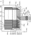
- FIG. 1 is a plan view of a light emitting device 1 according to an embodiment.
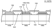
- FIG. 2 is a cross-sectional view taken along the line AA in FIG.
- the light emitting device 1 includes a plurality of first light emitting units 140a, a plurality of second light emitting units 140b, a plurality of third light emitting units 140c, and a control circuit 300.
- the plurality of first light emitting units 140a include an organic EL (electroluminescence) element that emits light of the first color, and specifically includes an organic material that emits light of the first color.
- the plurality of second light emitting units 140b includes an organic EL element that emits light of a second color different from the first color, and specifically includes an organic material that emits light of the second color.
- the plurality of second light emitting units 140b are adjacent to the plurality of first light emitting units 140a, respectively.
- the plurality of third light emitting units 140c include organic EL elements that emit light of a third color different from both the first color and the second color, and specifically, an organic material that emits light of the third color. Is included.
- the plurality of third light emitting units 140c are adjacent to the plurality of first light emitting units 140a and the plurality of second light emitting units 140b, respectively.
- the control circuit 300 causes the plurality of first light emitting units 140a to emit light, but does not cause the plurality of second light emitting units 140b and the plurality of third light emitting units 140c to emit light.
- An element for selectively projecting light in a region for example, an LCD element (for example, a reflective LCD element (for example, LCOS (Liquid Crystal On Silicon)) or a transmissive LCD element)
- LCD element for example, a reflective LCD element (for example, LCOS (Liquid Crystal On Silicon)) or a transmissive LCD element)
- a first image can be generated from the light
- a second image can be generated from the light of the second color
- a third image can be generated from the light of the third color.
- the first image, the second image, and the third image One color image can be generated by combining.
- the light emitting device 1 can function as a light source for an FSC display.
- the light emitting device 1 includes a light emitting plate 10, a wiring board 200, and a control circuit 300.
- the light emitting plate 10 includes a substrate 100, a plurality of first light emitting units 140a, a plurality of second light emitting units 140b, a plurality of third light emitting units 140c, an electrode 160, a plurality of first connection wirings 162a, and a plurality of second connection wirings 162b.
- a plurality of third connection wirings 162c and two connection wirings 162g are included.
- the wiring substrate 200 includes a base 210, a plurality of first connection wires 262a, a plurality of second connection wires 262b, a plurality of third connection wires 262c, a first wire 264a, a second wire 264b, a third wire 264c, a wire 264g, A first terminal 266a, a second terminal 266b, a third terminal 266c, and a terminal 266g are included.
- the substrate 100 has a substantially rectangular shape.
- the substrate 100 has a first side 106a, a second side 106b, a third side 106c, and a fourth side 106d.
- the first side 106a extends in one direction (Y direction in the figure).
- the second side 106b is on the opposite side of the first side 106a.
- the third side 106c is between the first side 106a and the second side 106b and extends in a direction intersecting the first side 106a (X direction in the drawing).
- the fourth side 106d is on the opposite side of the third side 106c.
- Each of the third side 106c and the fourth side 106d is longer than each of the first side 106a and the second side 106b.
- the substrate 100 may have a shape different from a rectangle.
- the plurality of first light emitting units 140a, the plurality of second light emitting units 140b, and the plurality of third light emitting units 140c constitute a light emitting region 142.
- the plurality of first light emitting units 140a, the plurality of second light emitting units 140b, and the plurality of third light emitting units 140c are arranged in stripes.
- the plurality of first light emitting units 140a, the plurality of second light emitting units 140b, and the plurality of third light emitting units 140c extend in one direction (the Y direction in the drawing) and intersect in this one direction. They are lined up along the direction (X direction in the figure).
- the light emitting region 142 is longer in the arrangement direction (X direction in the drawing) of the light emitting units than in the extending direction (Y direction in the drawing) of the light emitting units.
- the plurality of first light emitting units 140a, the plurality of second light emitting units 140b, and the plurality of third light emitting units 140c are arranged in a regular order, that is, the first light emitting unit 140a and the second light emitting unit 140b.
- the third light emitting unit 140c is repeatedly arranged in this order.
- the plurality of first light emitting units 140a, the plurality of second light emitting units 140b, and the plurality of third light emitting units 140c may be arranged in an irregular order at least in part.
- the electrode 160 is shared by the plurality of first light emitting units 140a, the plurality of second light emitting units 140b, and the plurality of third light emitting units 140c.
- the voltage applied to the electrode 160 can be applied to all of the plurality of first light emitting units 140a, the plurality of second light emitting units 140b, and the plurality of third light emitting units 140c.
- the plurality of first connection wires 162a are respectively connected to the plurality of first light emitting portions 140a, and the plurality of second connection wires 162b are respectively connected to the plurality of second light emitting portions 140b, and the plurality of third light emitting portions 140a are connected to each other.
- the connection wiring 162c is connected to each of the plurality of third light emitting units 140c.
- One of the two connection wirings 162g is connected to one end of the electrode 160, and the other of the two connection wirings 162g is connected to the other end of the electrode 160.
- the one end and the other end of the electrode 160 are positioned on opposite sides in the arrangement direction (X direction in the drawing) of the plurality of first light emitting units 140a, the plurality of second light emitting units 140b, and the plurality of third light emitting units 140c. doing.
- a voltage can be applied to both ends of the electrode 160 by the two connection wirings 162g. Therefore, variation in voltage distribution in the electrode 160 can be suppressed.
- the wiring board 200 is disposed along the third side 106 c of the board 100.
- the plurality of first connection wirings 262 a of the wiring substrate 200 are respectively connected to the plurality of first connection wirings 162 a of the substrate 100, and the plurality of second connection wirings 262 b of the wiring substrate 200 are connected to the plurality of second connection wirings 262 b of the substrate 100.
- the plurality of third connection wirings 262c of the wiring substrate 200 are connected to the plurality of third connection wirings 162c of the substrate 100, respectively.
- the first wiring 264a of the wiring board 200 is connected to the plurality of first connection wirings 262a, and the second wiring 264b of the wiring board 200 is connected to the plurality of second connection wirings 262b.
- the third wiring 264c is connected to a plurality of third connection wirings 262c.
- One end of the wiring 264g of the wiring board 200 is connected to one connection wiring 162g, and the other end of the wiring 264g of the wiring board 200 is connected to the other connection wiring 162g.
- the first terminal 266a of the wiring board 200 is connected to the first wiring 264a
- the second terminal 266b of the wiring board 200 is connected to the second wiring 264b
- the third terminal 266c of the wiring board 200 is It is connected to the third wiring 264c
- the terminal 266g of the wiring board 200 is connected to the wiring 264g.
- the control circuit 300 can apply a voltage for causing the plurality of first light emitting units 140a to emit light to the first terminal 266a at the first timing, and cause the plurality of second light emitting units 140b to emit light at the second timing. For this reason, a voltage for causing the plurality of third light emitting units 140c to emit light can be applied to the third terminal 266c at the third timing.
- the control circuit 300 can apply the reference potential (for example, ground potential) for the voltage described above to the terminal 266g at any of the first timing, the second timing, and the third timing.
- a plurality of light emitting units by applying a voltage to the first terminal 266a, the second terminal 266b, or the third terminal 266c, a plurality of first light emitting units 140a, a plurality of second light emitting units 140b, and a plurality of Any one of the third light emitting units 140c can selectively emit light. Therefore, it is not necessary to provide an element (for example, a thin film transistor (TFT)) for controlling each light emitting unit in each light emitting unit. Therefore, the control of the plurality of light emitting units can be facilitated.
- TFT thin film transistor
- the substrate 100 has a first surface 102 and a second surface 104.
- the first electrode 110, the organic layer 120, the second electrode 130, and the insulating layer 150 are located on the first surface 102 of the substrate 100.
- the second surface 104 is on the opposite side of the first surface 102.
- the insulating layer 150 has an opening 152.
- the opening 152 of the insulating layer 150 defines a first light emitting unit 140a, a second light emitting unit 140b, and a third light emitting unit 140c.
- the first electrode 110, the organic layer 120, and the second electrode 130 are stacked to constitute the first light emitting unit 140a, the second light emitting unit 140b, or the third light emitting unit 140c.
- the plurality of first light emitting units 140a, the plurality of second light emitting units 140b, and the plurality of third light emitting units 140c are located on the first surface 102 of the substrate 100, and the first surface of the substrate 100 is It is repeatedly arranged along the line 102.
- the substrate 100 is made of, for example, glass or resin.
- the substrate 100 may or may not have flexibility.
- the substrate 100 may or may not have a light-transmitting property.
- the first electrode 110 functions as an anode.
- the first electrode 110 may have a light-transmitting property or may not have a light-transmitting property.
- the organic layer 120 includes a light emitting layer (EML) capable of emitting light by organic electroluminescence (EL).
- EML light emitting layer
- the EML of the first light emitting unit 140a, the EML of the second light emitting unit 140b, and the EML of the third light emitting unit 140c contain different organic materials. Accordingly, the first light emitting unit 140a, the second light emitting unit 140b, and the third light emitting unit 140c can emit different colors of light.
- the organic layer 120 may appropriately include a hole injection layer (HIL), a hole transport layer (HTL), an electron transport layer (ETL), and an electron injection layer (EIL).
- the organic layer 120 may further include a charge generation layer (CGL).
- the second electrode 130 functions as a cathode.
- the second electrode 130 may have a light-transmitting property or may not have a light-transmitting property.
- the first electrode 110 may have a light shielding property
- the second electrode 130 may have a light transmitting property, particularly a light reflecting property.
- the light emitted from the organic layer 120 passes through the second electrode 130 and is emitted from the opposite side of the second surface 104 of the substrate 100.
- the first electrode 110 when the first electrode 110 includes a translucent conductive material, the first electrode 110 can have translucency.
- the transparent conductive material is, for example, a metal oxide (for example, ITO (Indium Tin Oxide), IZO (Indium Zinc Oxide), IWZO (Indium Tungsten Zinc Oxide), ZnO (Zinc Oxide), or IGZO (IndiumGaliumZium Oxide).
- a carbon nanotube or a conductive polymer for example, PEDOT.
- the first electrode 110 when the first electrode 110 is formed of a metal thin film (for example, Ag) or an alloy thin film (for example, AgMg), the first electrode 110 may have a light transmitting property. The same applies to the second electrode 130.
- the first electrode 110 when the first electrode 110 includes a light-shielding conductive material, particularly a light-reflective conductive material, the first electrode 110 can have a light-shielding property, particularly a light-reflecting property.
- the light-shielding conductive material is a metal or an alloy, and more specifically, at least one metal selected from the group consisting of Al, Au, Ag, Pt, Mg, Sn, Zn, and In or An alloy of metals selected from this group. The same applies to the second electrode 130.
- the light emitting plate 10 When the conductivity of the first electrode 110 is low, for example, when the first electrode 110 includes a translucent conductive material, the light emitting plate 10 includes a conductive layer (not shown) that functions as an auxiliary electrode of the first electrode 110. You may go out.
- the conductive layer may be covered with the first electrode 110, or may be covered with the insulating layer 150 on the first electrode 110.
- the conductive layer is, for example, MAM (Mo / Al / Mo).
- the first electrode 110 of the first light emitting unit 140a, the first electrode 110 of the second light emitting unit 140b, and the first electrode 110 of the third light emitting unit 140c are separated from each other.
- the organic layer 120 of the first light emitting unit 140a, the organic layer 120 of the second light emitting unit 140b, and the organic layer 120 of the third light emitting unit 140c are separated from each other and include different light emitting layers (EML).
- the second electrode 130 is shared by the first light emitting unit 140a, the second light emitting unit 140b, and the third light emitting unit 140c, and the first electrode 110 of the first light emitting unit 140a and the first electrode 110 of the second light emitting unit 140b.
- the first electrode 110 and the insulating layer 150 of the third light emitting unit 140c are covered.
- the first electrode 110 of the first light emitting unit 140a is connected to the first connection wiring 162a shown in FIG. 1, and the first electrode 110 of the second light emitting unit 140b is connected to the second connection wiring 162b shown in FIG.
- the first electrode 110 of the third light emitting unit 140c is connected to the third connection wiring 162c shown in FIG.
- the second electrode 130 is the electrode 160 shown in FIG. 1, and is connected to the two connection wirings 162g shown in FIG.
- the first electrode 110 of each light emitting unit may be formed integrally with the connection wiring (the first connection wiring 162a, the second connection wiring 162b, or the third connection wiring 162c).
- a conductive pattern is located on the first surface 102 of the substrate 100, one region of this conductive pattern functions as the first electrode 110, and the other region of this conductive pattern functions as a connection wiring. To do.
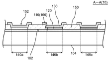
- FIG. 3 is a diagram showing a modification of FIG.
- the example shown in FIG. 3 is the same as the example shown in FIG. 2 except for the following points.
- the first electrode 110 is shared by the first light emitting unit 140a, the second light emitting unit 140b, and the third light emitting unit 140c, and the organic layer 120 and the second electrode 130 are located on the first electrode 110.
- the second electrode 130 of the first light emitting unit 140a, the second electrode 130 of the second light emitting unit 140b, and the second electrode 130 of the third light emitting unit 140c are separated from each other.
- the second electrode 130 may be divided by forming a partition between the first light emitting unit 140a, the second light emitting unit 140b, and the third light emitting unit 140c.
- the first electrode 110 is the electrode 160 shown in FIG. 1, and is connected to the two connection wirings 162g shown in FIG.
- the second electrode 130 of the first light emitting unit 140a is connected to the first connection wiring 162a shown in FIG. 1, and the second electrode 130 of the second light emitting unit 140b is connected to the second connection wiring 162b shown in FIG.
- the second electrode 130 of the third light emitting unit 140c is connected to the third connection wiring 162c shown in FIG.
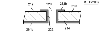
- FIG. 4 is an enlarged plan view of a part of the wiring board 200 shown in FIG. 5 is a cross-sectional view taken along the line BB of FIG.
- the wiring board 200 is a flexible printed circuit (FPC). Therefore, the wiring board 200 can be deformed with a high degree of freedom.
- FPC flexible printed circuit
- the wiring board 200 includes a base 210.
- the base 210 has electrical insulation.
- the base 210 has a first surface 212 and a second surface 214.
- the second surface 214 is on the opposite side of the first surface 212.
- the base 210 has a through hole 220.
- the through hole 220 passes through the base 210 from the first surface 212 to the second surface 214.
- the second connection wiring 262 b is located on the first surface 212 of the base 210, and the second wiring 264 b is located on the second surface 214 of the base 210.
- the second connection wiring 262b and the second wiring 264b are connected to each other through a conductive layer 222 formed on the side surface of the through hole 220.
- the first connection wiring 262a and the first wiring 264a are connected to each other in the same manner as the second connection wiring 262b and the second wiring 264b, and the third connection wiring 262c and the third wiring 264c are connected to the second connection wiring 262b and the second connection wiring 262b. Similar to the second wiring 264b, they are connected to each other.
- the through hole 220 (first through hole 220a) for connecting the first connection wiring 262a and the first wiring 264a, the second connection wiring 262b and the second wiring 264b are connected to each other.
- the through hole 220 (second through hole 220b), the third connection wiring 262c and the third wiring 264c for connecting the through hole 220 (third through hole 220c) to each other along the Y direction in the figure. It is in a line. Therefore, a set of the first through hole 220a, the second through hole 220b, and the third through hole 220c can be arranged in a small space along the X direction in the drawing.
- the second connection wiring 262b includes a portion extending around the third through hole 220c. Therefore, interference of the third through hole 220c due to the second connection wiring 262b can be prevented.
- the first connection wiring 262a includes a portion extending around the third through hole 220c and the second through hole 220b. Therefore, interference between the third through hole 220c and the second through hole 220b due to the first connection wiring 262a can be prevented.
- the base 210 separates the first connection wiring 262a and the second wiring 264b from each other in the overlapping region of the first connection wiring 262a and the second wiring 264b, and in the overlapping region of the first connection wiring 262a and the third wiring 264c.
- the first connection wiring 262a and the third wiring 264c are separated from each other. Therefore, the interconnection of the first connection wiring 262a and the second wiring 264b and the interconnection of the first connection wiring 262a and the third wiring 264c can be prevented.
- the base 210 separates the second connection wiring 262b and the third wiring 264c from each other in an overlapping region of the second connection wiring 262b and the third wiring 264c. Therefore, mutual connection between the second connection wiring 262b and the third wiring 264c can be prevented.
- FIG. 6 is a diagram showing a first modification of FIG.
- the example shown in FIG. 6 is the same as the example shown in FIG. 1 except for the following points.
- the light emitting device 1 can function as a surface light source that emits light of the first color by light emission of the plurality of first light emitting units 140a at the first timing, and a plurality of light emitting devices 1 at the second timing. It can function as a surface light source that emits light of the second color by light emission of the second light emitting unit 140b, and functions as a surface light source that emits light of the third color by light emission of the plurality of third light emitting units 140c at the third timing. It can function as a surface light source that emits light of the fourth color by light emission of the plurality of fourth light emitting units 140d at the fourth timing. In this way, the light emitting device 1 can function as a light source for an FSC display.
- the first color can be red (R), the second color can be green (G), the third color can be blue (B), and the fourth color can be yellow (Y).
- the first color is red (R), the second color is green (G), the third color is blue (B), and the fourth color is white (W). Can do.
- the plurality of first light emitting units 140a, the plurality of second light emitting units 140b, the plurality of third light emitting units 140c, and the plurality of fourth light emitting units 140d are arranged in a regular order, that is, the first light emitting units.
- the unit 140a, the second light emitting unit 140b, the third light emitting unit 140c, and the fourth light emitting unit 140d are repeatedly arranged in this order.
- the plurality of first light emitting units 140a, the plurality of second light emitting units 140b, the plurality of third light emitting units 140c, and the plurality of fourth light emitting units 140d may be arranged in an irregular order at least partially. .
- the light emitting device 1 includes a plurality of fourth connection wirings 162d.
- the plurality of fourth connection wirings 162d are connected to the plurality of fourth light emitting units 140d, respectively.
- the wiring board 200 includes a plurality of fourth connection wirings 262d, fourth wirings 264d, and fourth terminals 266d.
- the plurality of fourth connection wirings 262d of the wiring substrate 200 are connected to the plurality of fourth connection wirings 162d of the substrate 100, respectively.
- the fourth wiring 264d is connected to the plurality of fourth connection wirings 262d.
- the fourth terminal 266d is connected to the fourth wiring 264d.
- the control circuit 300 can apply a voltage for causing the plurality of fourth light emitting units 140d to emit light to the fourth terminal 266d at the fourth timing.
- the plurality of first light emitting units 140a, the plurality of second light emitting units 140b, the plurality of third light emitting units 140c, and the plurality of fourth light emitting units 140d are separated from each other as shown in FIG. And may share the second electrode 130 (electrode 160), or may include a plurality of second electrodes 130 separated from each other and the second electrode 130 (electrode 160), as shown in FIG. May be shared.
- FIG. 7 is a diagram showing a second modification of FIG.
- the example shown in FIG. 7 is the same as the example shown in FIG. 1 except for the following points.
- the outline of the light emitting device 1 will be described with reference to FIGS.
- the light emitting device 1 includes a plurality of first connection wirings 162a, a plurality of second connection wirings 162b, and a plurality of third connection wirings 162c.
- the plurality of first connection wirings 162a, the plurality of second connection wirings 162b, and the plurality of third connection wirings 162c are arranged together.
- the light emitting device 1 includes a first wiring 164a, a second wiring 164b, and a third wiring 164c. As shown in FIG.
- the second light emitting unit 140b and the third light emitting unit 140c have translucency. doing. Accordingly, the light emitted from each first light emitting unit 140a is transmitted through the second substrate 100b, the second light emitting unit 140b, the third substrate 100c, and the third light emitting unit 140c and is transmitted through the second surface 104 of the first substrate 100a.
- the light emitted from the opposite side (the first surface 102 side of the third substrate 100c), and the light emitted from each second light emitting unit 140b passes through the third substrate 100c and the third light emitting unit 140c and passes through the third light emitting unit 140c.
- the light can be emitted from the opposite side of the second surface 104 of the first substrate 100a (the first surface 102 side of the third substrate 100c).
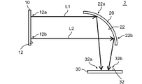
- the light having the peak luminous intensity (light L2) in the light distribution of the second region 12b of the light irradiation surface 12 is sent to the second region 32b of the target surface 32 via the second region 22b of the reflection surface 22.
- the optical distance from the first region 12a of the light irradiation surface 12 to the first region 32a of the target surface 32 via the first region 22a of the reflection surface 22 is from the second region 12b of the light irradiation surface 12 to the reflection surface 22. This is larger than the optical distance from the second region 22b to the second region 32b of the target surface 32.
- the light intensity of the light L1 is larger than the light intensity of the light L2.
- the light L1 is emitted along the normal direction of the first region 12a of the light irradiation surface 12, and the light L2 is in the normal direction of the second region 12b of the light irradiation surface 12. It is emitted along.
- the light L1 that is, light having a peak luminous intensity in the light distribution of the first region 12a of the light irradiation surface 12 is along a direction inclined from the normal direction of the first region 12a of the light irradiation surface 12. It may be emitted.
- the direction of the peak luminous intensity in the light distribution can be adjusted by adjusting the thickness of each layer of the organic layer 120 (FIG. 2 or FIG. 3) included in the light emitting plate 10. The same applies to the light L2.
- the light emitting plate 10 can function as a light source of an FSC display as described using the embodiment.
- the light emitting plate 10 emits light of a first color (for example, red (R)) at the first timing, and the second color (for example, green (G)) at the second timing.
- the light of the third color e.g., blue (B)
- the object 30 e.g., LCOS
- a first image is generated by selecting a part of the light of the second color
- a second image is generated by selecting a part of the light of the second color irradiated on the target surface 32 at the second timing.
- the third image is generated by selecting a part of the third color light irradiated on the target surface 32.
- One color image can be generated by combining the first image, the second image, and the third image.
- the light emitting module 2 can be used for a head-up display (HUD).
- This HUD can be mounted on, for example, an automobile.
- the reflecting member 20 is a mirror
- the object 30 is a transparent display for projecting an image.
- the HUD is mounted on an automobile, it can be a windshield, for example.
- FIG. 17 is a diagram showing an example of the layout of the light irradiation surface 12 of the light emitting plate 10 shown in FIG.
- the area of the first region 12a of the light irradiation surface 12 is equal to the area of the second region 12b of the light irradiation surface 12.
- the area of the light emitting unit 140 occupying the first region 12a is larger than the area of the light emitting unit 140 occupying the second region 12b. Therefore, the light intensity of the light L1 (light irradiated from the first region 12a (FIG. 16)) can be made larger than the light intensity of the light L2 (light irradiated from the second region 12b (FIG. 17)).
- FIG. 18 is a diagram illustrating the light emitting module 2 according to the second embodiment.
- the light emitting module 2 according to Example 2 is the same as the light emitting module 2 according to Example 1 except for the following points.
- the light intensity of the light L1 is substantially equal to the light intensity of the light L2.
- the normal direction in the first region 22 a of the reflective surface 22 is different from the normal direction in the second region 22 b of the reflective surface 22.
- the optical distance from the first region 12a of the light irradiation surface 12 to the first region 32a of the target surface 32 via the first region 22a of the reflection surface 22 is from the second region 12b of the light irradiation surface 12 to the reflection surface 22.
- the optical distance from the second region 22b to the second region 32b of the target surface 32 is substantially equal. In the example shown in FIG.
- the first region 12a of the light irradiation surface 12 passes through the first region 22a of the reflection surface 22.
- the physical distance of the target surface 32 to the first region 32a is the physical distance from the second region 12b of the light irradiation surface 12 to the second region 32b of the target surface 32 via the second region 22b of the reflective surface 22. And substantially equal.
- the optical distance of the light L1 is substantially equal to the optical distance of the light L2. In this way, variations in the luminance distribution of the target surface 32 can be suppressed. In addition, the degree of freedom in designing the arrangement of the reflecting member 20 and the object 30 and the shape of the reflecting member 20 can be improved.
- the light L1 is emitted in a direction different from the light L2 in order to make the physical distance about the light L1 equal to the physical distance about the light L2.
- the light L1 is emitted along the normal direction in the first region 12a of the light irradiation surface 12, and the light L2 is emitted along the normal direction in the first region 12a of the light irradiation surface 12.
- the light irradiation surface 12 is curved.
- the physical distance from the first region 12 a of the light irradiation surface 12 to the first region 32 a of the target surface 32 via the first region 22 a of the reflection surface 22 is from the second region 12 b of the light irradiation surface 12 to the reflection surface 22.
- the physical distance to the second region 32b of the target surface 32 via the second region 22b is larger.
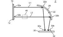
- the optical path from the second region 12b of the light irradiation surface 12 to the second region 32b of the target surface 32 via the second region 22b of the reflecting surface 22 is a first path portion having a first refractive index (high refraction). And a second path portion (high refractive index region 40) having a second refractive index higher than the first refractive index.
- the optical distance of the light L1 is substantially equal to the optical distance of the light L2 by adjusting the length and refractive index of the second path portion (high refractive index region 40) for the light L2. Can be made equal to Therefore, variations in the luminance distribution of the target surface 32 can be suppressed.
- the first path portion portion other than the high refractive index region 40
- the second path portion is, for example, more than air. It can be a medium having a high refractive index (for example, glass, water or resin).
- FSC field sequential color
- LCD liquid crystal displays
- a plurality of first light emitting units including an organic EL element that emits light of a first color
- a plurality of second light emitting units each including an organic EL element that emits light of a second color different from the first color, each adjacent to the plurality of first light emitting units
- a control circuit includes: In the first timing, the plurality of first light emitting units emit light while the plurality of second light emitting units do not emit light, A light emitting device that causes the plurality of second light emitting units to emit light while the plurality of first light emitting units do not emit light at the second timing. 1-2. 1-1.
- the light-emitting device described in Further comprising a substrate having a first surface; The plurality of first light emitting units and the plurality of second light emitting units are arranged along the first surface of the substrate. 1-3. 1-2.
- An organic EL element that emits light of a third color different from both the first color and the second color, and the plurality of first light emitting units and the plurality of second light sources along the first surface of the substrate.
- the light-emitting devices are arranged in order. 1-5. 1-3. Or 1-4.
- the first color is red;
- the second color is green;
- the light emitting device, wherein the third color is blue. 1-6. 1-3.
- An organic EL element that emits light of a fourth color different from any of the first color, the second color, and the third color, and the plurality of first light emitting units along the first surface of the substrate;
- a plurality of fourth light emitting units arranged together with the plurality of second light emitting units and the plurality of third light emitting units;
- the control circuit includes: In the first timing, the second timing, and the third timing, the plurality of fourth light emitting units are not caused to emit light, In a fourth timing, the plurality of fourth light emitting units emit light, and the plurality of first light emitting units, the plurality of second light emitting units, and the plurality of third light emitting units do not emit light. 1-7. 1-6.
- the plurality of first light emitting units each include a plurality of first electrodes spaced apart from each other
- the plurality of second light emitting units each include a plurality of first electrodes spaced apart from each other.
- the plurality of first light emitting units and the plurality of second light emitting units are common to cover the plurality of first electrodes of the plurality of first light emitting units and the plurality of first electrodes of the plurality of second light emitting units.
- the plurality of first connection wirings, the plurality of second connection wirings, and the plurality of third connection wirings are repeatedly arranged in the order of the first connection wiring, the second connection wiring, and the third connection wiring. apparatus. 2-5. 2-3. Or 2-4.
- the first color is red;
- the second color is green;
- the light emitting device, wherein the third color is blue. 2-6. 2-3.
- a plurality of fourth light emitting units including organic EL elements that emit light of a fourth color, located on the first surface of the substrate; Located on the first surface of the substrate and connected to the plurality of fourth light emitting sections, together with the plurality of first connection wirings, the plurality of second connection wirings, and the plurality of third connection wirings A plurality of fourth connection wires arranged; A fourth wiring located on the first surface of the substrate and connected to the plurality of fourth connection wirings; A light emitting device further comprising: 2-7. 2-6.
- the plurality of first connection lines, the plurality of second connection lines, the plurality of third connection lines, and the plurality of fourth connection lines are the first connection line, the second connection line, and the third connection line.
- a light emitting device that is repeatedly arranged in the order of the fourth connection wiring 2-8. 2-6. Or 2-7.
- the first color is red;
- the second color is green;
- the third color is blue;
- the light emitting device, wherein the fourth color is yellow. 2-9. 2-1.
Landscapes
- Engineering & Computer Science (AREA)
- General Engineering & Computer Science (AREA)
- Physics & Mathematics (AREA)
- Microelectronics & Electronic Packaging (AREA)
- Optics & Photonics (AREA)
- Electroluminescent Light Sources (AREA)
- Liquid Crystal (AREA)
- Devices For Indicating Variable Information By Combining Individual Elements (AREA)
Abstract
光照射面(12)の第1領域(12a)の配光分布におけるピーク光度の光(光(L1))は、反射面(22)の第1領域(22a)を経由して対象面(32)の第1領域(32a)に送られる。光照射面(12)の第2領域(12b)の配光分布におけるピーク光度の光(光(L2))は、反射面(22)の第2領域(22b)を経由して対象面(32)の第2領域(32b)に送られる。光照射面(12)の第1領域(12a)から反射面(22)の第1領域(22a)を経由して対象面(32)の第1領域(32a)までの光学的距離は、光照射面(12)の第2領域(12b)から反射面(22)の第2領域(22b)を経由して対象面(32)の第2領域(32b)までの光学的距離より大きくなっている。光(L1)の光度は、光(L2)の光度より大きくなっている。
Description
本発明は、発光モジュールに関する。
近年、LCOS(Liquid Crystal On Silicon)を有するディスプレイが開発されている。このディスプレイは、例えば、ヘッドアップディスプレイ(HUD)、ヘッドマウントディスプレイ(HMD)、電子ビューファインダ(EVF)又はプロジェクタに利用することができる。
特許文献1には、LCOSを有するディスプレイの一例について記載されている。このディスプレイでは、光源から発せられた光を偏光ビームスプリッタ(PBS)によってLCOSに向けて反射させる。PBSは、光源から発せられた光のS偏光をLCOSに向けて反射する。LCOSの一の領域は、PBSから反射されたS偏光の偏光方向を変えないまま、このS偏光をPBSに向けて戻し、LCOSの他の一の領域は、PBSから反射されたS偏光をP偏光に変換して、このP偏光をPBSに向けて戻す。PBSに向けて戻されたS偏光はPBSを透過しない一方で、PBSに向けて戻されたP偏光はPBSを透過する。LCOSの上述した一の領域及び他の一領域をLCOS内の回路によって制御することで、所望の画像を表示することができる。
特許文献2には、有機発光ダイオード(OLED)を有する表示装置が記載されている。この表示装置は、導光板及び反射型液晶ディスプレイ(LCD)素子を有している。導光板は、凹凸が形成された第1面及び端面を有している。導光板は、第1面が反射型LCD素子に対向するように、反射型LCD素子と重なっている。OLEDから発せられた光は、導光板の端面に入射し、導光板の第1面の凹凸から出射され、反射型LCD素子に入射する。
様々な発光モジュール(例えば、反射型LCD又はヘッドアップディスプレイ(HUD))において、発光板の光照射面から出射された光を反射部材の反射面によって対象物の対象面に向けて反射することがある。本発明者は、発光モジュールの光学系の条件によっては、対象面の輝度分布のばらつきが生じ得ることを見出した。
本発明が解決しようとする課題としては、対象面の輝度分布のばらつきを抑えることが一例として挙げられる。
請求項1に記載の発明は、
光照射面を有する発光板と、
前記発光板の前記光照射面から発せられた光を対象物の対象面に向けて反射するための反射面を有する反射部材と、
を含み、
前記光照射面の第1領域の配光分布におけるピーク光度の光は、前記反射面の第1領域を経由して前記対象面の第1領域に送られ、
前記光照射面の第2領域の配光分布におけるピーク光度の光は、前記反射面の第2領域を経由して前記対象面の第2領域に送られ、
前記光照射面の前記第1領域から前記反射面の前記第1領域を経由して前記対象面の前記第1領域までの光学的距離は、前記光照射面の前記第2領域から前記反射面の前記第2領域を経由して前記対象面の前記第2領域までの光学的距離より大きく、
前記光照射面の前記第1領域の前記配光分布における前記ピーク光度は、前記光照射面の前記第2領域の前記配光分布における前記ピーク光度より大きい、発光モジュールである。
光照射面を有する発光板と、
前記発光板の前記光照射面から発せられた光を対象物の対象面に向けて反射するための反射面を有する反射部材と、
を含み、
前記光照射面の第1領域の配光分布におけるピーク光度の光は、前記反射面の第1領域を経由して前記対象面の第1領域に送られ、
前記光照射面の第2領域の配光分布におけるピーク光度の光は、前記反射面の第2領域を経由して前記対象面の第2領域に送られ、
前記光照射面の前記第1領域から前記反射面の前記第1領域を経由して前記対象面の前記第1領域までの光学的距離は、前記光照射面の前記第2領域から前記反射面の前記第2領域を経由して前記対象面の前記第2領域までの光学的距離より大きく、
前記光照射面の前記第1領域の前記配光分布における前記ピーク光度は、前記光照射面の前記第2領域の前記配光分布における前記ピーク光度より大きい、発光モジュールである。
請求項5に記載の発明は、
光照射面を有する発光板と、
前記発光板の前記光照射面から発せられた光を対象物の対象面に向けて反射するための反射面を有する反射部材と、
を含み、
前記光照射面の第1領域の配光分布におけるピーク光度の光は、前記反射面の第1領域を経由して前記対象面の第1領域に送られ、
前記光照射面の第2領域の配光分布におけるピーク光度の光は、前記反射面の第2領域を経由して前記対象面の第2領域に送られ、
前記光照射面の前記第1領域の前記配光分布における前記ピーク光度は、前記光照射面の前記第2領域の前記配光分布における前記ピーク光度と実質的に等しく、
前記反射面の前記第1領域における法線方向は、前記反射面の前記第2領域における法線方向と異なっており、
前記光照射面の前記第1領域から前記反射面の前記第1領域を経由して前記対象面の前記第1領域までの光学的距離は、前記光照射面の前記第2領域から前記反射面の前記第2領域を経由して前記対象面の前記第2領域までの光学的距離と実質的に等しい、発光モジュールである。
光照射面を有する発光板と、
前記発光板の前記光照射面から発せられた光を対象物の対象面に向けて反射するための反射面を有する反射部材と、
を含み、
前記光照射面の第1領域の配光分布におけるピーク光度の光は、前記反射面の第1領域を経由して前記対象面の第1領域に送られ、
前記光照射面の第2領域の配光分布におけるピーク光度の光は、前記反射面の第2領域を経由して前記対象面の第2領域に送られ、
前記光照射面の前記第1領域の前記配光分布における前記ピーク光度は、前記光照射面の前記第2領域の前記配光分布における前記ピーク光度と実質的に等しく、
前記反射面の前記第1領域における法線方向は、前記反射面の前記第2領域における法線方向と異なっており、
前記光照射面の前記第1領域から前記反射面の前記第1領域を経由して前記対象面の前記第1領域までの光学的距離は、前記光照射面の前記第2領域から前記反射面の前記第2領域を経由して前記対象面の前記第2領域までの光学的距離と実質的に等しい、発光モジュールである。
上述した目的、およびその他の目的、特徴および利点は、以下に述べる好適な実施の形態、およびそれに付随する以下の図面によってさらに明らかになる。
以下、本発明の実施の形態について、図面を用いて説明する。尚、すべての図面において、同様な構成要素には同様の符号を付し、適宜説明を省略する。
図1は、実施形態に係る発光装置1の平面図である。図2は、図1のA-A断面図である。
図1を用いて、発光装置1の概要を説明する。発光装置1は、複数の第1発光部140a、複数の第2発光部140b、複数の第3発光部140c及び制御回路300を含んでいる。複数の第1発光部140aは、第1色の光を発する有機EL(エレクトロルミネッセンス)素子を含んでおり、具体的には、第1の色の光を発する有機材料を含んでいる。複数の第2発光部140bは、第1色と異なる第2色の光を発する有機EL素子を含んでおり、具体的には、第2の色の光を発する有機材料を含んでいる。複数の第2発光部140bは、複数の第1発光部140aとそれぞれ隣り合っている。複数の第3発光部140cは、第1色及び第2色のいずれとも異なる第3色の光を発する有機EL素子を含んでおり、具体的には、第3の色の光を発する有機材料を含んでいる。複数の第3発光部140cは、複数の第1発光部140a及び複数の第2発光部140bとそれぞれ隣り合っている。制御回路300は、第1タイミングにおいて、複数の第1発光部140aを発光させる一方で複数の第2発光部140b及び複数の第3発光部140cを発光させない。制御回路300は、第2タイミングにおいて、複数の第2発光部140bを発光させる一方で複数の第1発光部140a及び複数の第3発光部140cを発光させない。制御回路300は、第3タイミングにおいて、複数の第3発光部140cを発光させる一方で複数の第1発光部140a及び複数の第2発光部140bを発光させない。一例において、制御回路300は、複数の第1発光部140aによる発光、複数の第2発光部140bによる発光及び複数の第3発光部140cによる発光を繰り返してもよい。
発光装置1は、フィールドシーケンシャルカラー(FSC)ディスプレイ(例えば、FSC液晶ディスプレイ(LCD))の光源として機能することができる。具体的には、発光装置1は、第1タイミングにおいて、複数の第1発光部140aの発光によって第1色の光を発する面光源として機能することができ、第2タイミングにおいて、複数の第2発光部140bの発光によって第2色の光を発する面光源として機能することができ、第3タイミングにおいて、複数の第3発光部140cの発光によって第3色の光を発する面光源として機能することができる。一領域の光を選択的に投影するための素子、例えば、LCD素子(例えば、反射型LCD素子(例えば、LCOS((Liquid Crystal On Silicon)))又は透過型LCD素子)によって、第1色の光から第1画像を生成し、第2色の光から第2画像を生成し、第3色の光から第3画像を生成することができ、第1画像、第2画像及び第3画像の合成によって1つのカラー画像を生成することができる。このようにして、発光装置1は、FSCディスプレイの光源として機能することができる。
図1に示す例では、発光装置1は、3色の光、すなわち、第1色の光、第2色の光及び第3色の光を発し、一例において、第1色は、赤色(R)とし、第2色は、緑色(G)とし、第3色は、青色(B)とすることができる。他の例において、発光装置1は、2色のみの光、例えば、第1色の光及び第2色の光のみを発してもよい。さらに他の例において、発光装置1は、3色よりも多い色(例えば、4色)の光を発してもよい。
図1を用いて、発光装置1の平面レイアウトの詳細を説明する。
発光装置1は、発光板10、配線基板200及び制御回路300を含んでいる。
発光板10は、基板100、複数の第1発光部140a、複数の第2発光部140b、複数の第3発光部140c、電極160、複数の第1接続配線162a、複数の第2接続配線162b、複数の第3接続配線162c及び2つの接続配線162gを含んでいる。
配線基板200は、ベース210、複数の第1接続配線262a、複数の第2接続配線262b、複数の第3接続配線262c、第1配線264a、第2配線264b、第3配線264c、配線264g、第1端子266a、第2端子266b、第3端子266c及び端子266gを含んでいる。
基板100は、実質的に矩形の形状を有している。基板100は、第1辺106a、第2辺106b、第3辺106c及び第4辺106dを有している。第1辺106aは、一方向(図内のY方向)に延伸している。第2辺106bは、第1辺106aの反対側にある。第3辺106cは、第1辺106a及び第2辺106bの間にあって、第1辺106aに交わる方向(図内のX方向)に延伸している。第4辺106dは、第3辺106cの反対側にある。第3辺106c及び第4辺106dのそれぞれは、第1辺106a及び第2辺106bのそれぞれより長くなっている。他の例において、基板100は、矩形とは異なる形状を有していてもよい。
複数の第1発光部140a、複数の第2発光部140b及び複数の第3発光部140cは、発光領域142を構成している。複数の第1発光部140a、複数の第2発光部140b及び複数の第3発光部140cは、ストライプ状に配置されている。具体的には、複数の第1発光部140a、複数の第2発光部140b及び複数の第3発光部140cは、一方向(図内のY方向)に延伸しており、この一方向に交わる方向(図内のX方向)に沿って一緒に並んでいる。発光領域142は、各発光部の配列方向(図内のX方向)において、各発光部の延伸方向(図内のY方向)よりも、長くなっている。
図1に示す例では、複数の第1発光部140a、複数の第2発光部140b及び複数の第3発光部140cは、規則的な順に、すなわち、第1発光部140a、第2発光部140b及び第3発光部140cの順に繰り返し並んでいる。他の例において、複数の第1発光部140a、複数の第2発光部140b及び複数の第3発光部140cは、少なくとも一部分において、不規則的な順に並んでいてもよい。
電極160は、複数の第1発光部140a、複数の第2発光部140b及び複数の第3発光部140cによって共有されており、複数の第1発光部140a、複数の第2発光部140b及び複数の第3発光部140cに亘って広がっている。電極160に印加された電圧は、複数の第1発光部140a、複数の第2発光部140b及び複数の第3発光部140cのすべてに印加することができる。
複数の第1接続配線162aは、複数の第1発光部140aにそれぞれ接続しており、複数の第2接続配線162bは、複数の第2発光部140bにそれぞれ接続しており、複数の第3接続配線162cは、複数の第3発光部140cにそれぞれ接続している。2つの接続配線162gのうちの一方は、電極160の一端に接続しており、2つの接続配線162gのうちのもう一方は、電極160のもう一端に接続している。電極160の当該一端及び当該もう一端は、複数の第1発光部140a、複数の第2発光部140b及び複数の第3発光部140cの配列方向(図内のX方向)において互いに反対側に位置している。2つの接続配線162gによって電極160の両端に電圧を印加することができる。したがって、電極160における電圧分布のばらつきを抑えることができる。
配線基板200は、基板100の第3辺106cに沿って配置されている。配線基板200の複数の第1接続配線262aは、基板100の複数の第1接続配線162aにそれぞれ接続しており、配線基板200の複数の第2接続配線262bは、基板100の複数の第2接続配線162bにそれぞれ接続しており、配線基板200の複数の第3接続配線262cは、基板100の複数の第3接続配線162cにそれぞれ接続している。
配線基板200の第1配線264aは、複数の第1接続配線262aに接続しており、配線基板200の第2配線264bは、複数の第2接続配線262bに接続しており、配線基板200の第3配線264cは、複数の第3接続配線262cに接続している。配線基板200の配線264gの一端は、一方の接続配線162gに接続しており、配線基板200の配線264gのもう一端は、もう一方の接続配線162gに接続している。
配線基板200の第1端子266aは、第1配線264aに接続しており、配線基板200の第2端子266bは、第2配線264bに接続しており、配線基板200の第3端子266cは、第3配線264cに接続しており、配線基板200の端子266gは、配線264gに接続している。
制御回路300は、第1タイミングにおいて、複数の第1発光部140aを発光させるための電圧を第1端子266aに印加することができ、第2タイミングにおいて、複数の第2発光部140bを発光させるための電圧を第2端子266bに印加することができ、第3タイミングにおいて、複数の第3発光部140cを発光させるための電圧を第3端子266cに印加することができる。制御回路300は、第1タイミング、第2タイミング及び第3タイミングのいずれにおいても、上述した電圧のための基準電位(例えば、接地電位)を端子266gに印加することができる。
上述した構成によれば、複数の発光部の制御を容易にすることができる。具体的には、上述した構成においては、第1端子266a、第2端子266b又は第3端子266cへの電圧の印加によって、複数の第1発光部140a、複数の第2発光部140b及び複数の第3発光部140cのいずれかを選択的に発光させることができる。したがって、各発光部を制御するための素子(例えば、薄膜トランジスタ(TFT))を各発光部に設ける必要がない。したがって、複数の発光部の制御を容易にすることができる。
図2を用いて、発光装置1の断面構造の詳細を説明する。
基板100は、第1面102及び第2面104を有している。基板100の第1面102上には、第1電極110、有機層120、第2電極130及び絶縁層150が位置している。第2面104は、第1面102の反対側にある。
絶縁層150は、開口152を有している。絶縁層150の開口152は、第1発光部140a、第2発光部140b及び第3発光部140cを画定している。絶縁層150の開口152において、第1電極110、有機層120及び第2電極130は、第1発光部140a、第2発光部140b又は第3発光部140cを構成するように積層されている。このようにして、複数の第1発光部140a、複数の第2発光部140b及び複数の第3発光部140cは、基板100の第1面102上に位置しており、基板100の第1面102に沿って一緒に繰り返し並んでいる。
基板100は、例えば、ガラス又は樹脂からなっている。基板100は、可撓性を有していてもよいし、又は有していなくてもよい。基板100は、透光性を有していてもよいし、又は有していなくてもよい。
第1電極110は、陽極として機能している。第1電極110は、透光性を有していてもよいし、又は透光性を有していなくてもよい。
有機層120は、有機エレクトロルミネッセンス(EL)により発光可能な発光層(EML)を含んでいる。第1発光部140aのEML、第2発光部140bのEML及び第3発光部140cのEMLは、互いに異なる有機材料を含んでいる。したがって、第1発光部140a、第2発光部140b及び第3発光部140cは、互いに異なる色の光を発することができる。有機層120は、正孔注入層(HIL)、正孔輸送層(HTL)、電子輸送層(ETL)及び電子注入層(EIL)を適宜含んでいてもよい。有機層120は、電荷発生層(CGL)をさらに含んでいてもよい。
第2電極130は、陰極として機能している。第2電極130は、透光性を有していてもよいし、又は透光性を有していなくてもよい。
一例において、第1電極110が透光性を有し、第2電極130が遮光性、特に光反射性を有していてもよい。この例において、有機層120から発せられた光は、第1電極110及び基板100を透過して基板100の第2面104から出射される。
他の例において、第1電極110が遮光性を有し、第2電極130が透光性、特に光反射性を有していてもよい。この例において、有機層120から発せられた光は、第2電極130を透過して基板100の第2面104の反対側から出射される。
さらに他の例において、第1電極110及び第2電極130の双方が透光性を有していてもよい。この例において、有機層120から発せられた光の一部は、第1電極110及び基板100を透過して基板100の第2面104から出射され、有機層120から発せられた光の他の一部は、第2電極130を透過して基板100の第2面104の反対側から出射される。
一例において、第1電極110が透光性導電材料を含む場合、第1電極110は、透光性を有することができる。透明導電材料は、例えば、金属酸化物(例えば、ITO(Indium Tin Oxide)、IZO(Indium Zinc Oxide)、IWZO(Indium Tungsten Zinc Oxide)、ZnO(Zinc Oxide))又はIGZO(Indium Galium Zinc Oxide)、カーボンナノチューブ又は導電性高分子(例えば、PEDOT)である。他の例において、第1電極110が金属薄膜(例えば、Ag)又は合金薄膜(例えば、AgMg)からなる場合、第1電極110は、透光性を有することができる。第2電極130についても同様である。
一例において、第1電極110が遮光性導電材料、特に光反射性導電材料を含む場合、第1電極110は、遮光性、特に光反射性を有することができる。一例において、遮光性導電材料は、金属又は合金であり、より具体的には、Al、Au、Ag、Pt、Mg、Sn、Zn及びInからなる群の中から選択される少なくとも1つの金属又はこの群から選択される金属の合金である。第2電極130についても同様である。
第1電極110の導電率が低い場合、例えば、第1電極110が透光性導電材料を含む場合、発光板10は、第1電極110の補助電極として機能する導電層(不図示)を含んでいてもよい。導電層は、第1電極110に覆われていてもよいし、又は第1電極110上において絶縁層150に覆われていてもよい。導電層は、例えば、MAM(Mo/Al/Mo)である。
第1発光部140aの第1電極110、第2発光部140bの第1電極110及び第3発光部140cの第1電極110は、互いに分離している。第1発光部140aの有機層120、第2発光部140bの有機層120及び第3発光部140cの有機層120は、互いに分離しており、互いに異なる発光層(EML)を含んでいる。第2電極130は、第1発光部140a、第2発光部140b及び第3発光部140cによって共有されており、第1発光部140aの第1電極110、第2発光部140bの第1電極110、第3発光部140cの第1電極110及び絶縁層150を覆っている。
第1発光部140aの第1電極110は、図1に示した第1接続配線162aに接続しており、第2発光部140bの第1電極110は、図1に示した第2接続配線162bに接続しており、第3発光部140cの第1電極110は、図1に示した第3接続配線162cに接続している。第2電極130は、図1に示した電極160であり、図1に示した2つの接続配線162gに接続している。
一例において、各発光部の第1電極110は、接続配線(第1接続配線162a、第2接続配線162b又は第3接続配線162c)と一体に形成されていてもよい。この例において、基板100の第1面102上には、導電パターンが位置しており、この導電パターンの一領域が第1電極110として機能し、この導電パターンの他の領域が接続配線として機能する。
図3は、図2の変形例を示す図である。図3に示す例は、以下の点を除いて、図2に示した例と同様である。
第1電極110は、第1発光部140a、第2発光部140b及び第3発光部140cによって共有されており、有機層120及び第2電極130が第1電極110上に位置している。第1発光部140aの第2電極130、第2発光部140bの第2電極130及び第3発光部140cの第2電極130は、互いに分離している。本図においては、第2電極130を金属マスクによって塗り分けする例を示したが、これに限定されない。他の例において、第1発光部140a、第2発光部140b及び第3発光部140cの間に隔壁を形成することで第2電極130を分断してもよい。
第1電極110は、図1に示した電極160であり、図1に示した2つの接続配線162gに接続している。第1発光部140aの第2電極130は、図1に示した第1接続配線162aに接続しており、第2発光部140bの第2電極130は、図1に示した第2接続配線162bに接続しており、第3発光部140cの第2電極130は、図1に示した第3接続配線162cに接続している。
図4は、図1に示した配線基板200の一部分の拡大平面図である。図5は、図4のB-B断面図である。
図4及び図5を用いて、配線基板200の詳細の一例を説明する。
図4及び図5に示す例において、配線基板200は、フレキシブルプリント回路(FPC)である。したがって、配線基板200は、高い自由度をもって変形させることができる。
配線基板200は、ベース210を含んでいる。ベース210は、電気的絶縁性を有している。ベース210は、第1面212及び第2面214を有している。第2面214は、第1面212の反対側にある。ベース210は、スルーホール220を有している。スルーホール220は、第1面212から第2面214にかけてベース210を貫通している。
図5に示すように、第2接続配線262bは、ベース210の第1面212上に位置しており、第2配線264bは、ベース210の第2面214上に位置している。第2接続配線262b及び第2配線264bは、スルーホール220の側面上に形成された導電層222を介して互いに接続している。第1接続配線262a及び第1配線264aは、第2接続配線262b及び第2配線264bと同様にして互いに接続しており、第3接続配線262c及び第3配線264cは、第2接続配線262b及び第2配線264bと同様にして互いに接続している。
図4に示すように、第1接続配線262a及び第1配線264aを相互に接続するためのスルーホール220(第1スルーホール220a)、第2接続配線262b及び第2配線264bを相互に接続するためのスルーホール220(第2スルーホール220b)、第3接続配線262c及び第3配線264cを相互に接続するためのスルーホール220(第3スルーホール220c)は、図内のY方向に沿って一列に並んでいる。したがって、第1スルーホール220a、第2スルーホール220b及び第3スルーホール220cの組を図内のX方向に沿って小スペース内に配置することができる。
第2接続配線262bは、第3スルーホール220cを迂回して延伸する部分を含んでいる。したがって、第2接続配線262bによる第3スルーホール220cの干渉を防ぐことができる。同様にして、第1接続配線262aは、第3スルーホール220c及び第2スルーホール220bを迂回して延伸する部分を含んでいる。したがって、第1接続配線262aによる第3スルーホール220c及び第2スルーホール220bの干渉を防ぐことができる。
ベース210は、第1接続配線262a及び第2配線264bの重なり領域において、第1接続配線262a及び第2配線264bを互いに隔てており、第1接続配線262a及び第3配線264cの重なり領域において、第1接続配線262a及び第3配線264cを互いに隔てている。したがって、第1接続配線262a及び第2配線264bの相互接続及び第1接続配線262a及び第3配線264cの相互接続を防ぐことができる。同様にして、ベース210は、第2接続配線262b及び第3配線264cの重なり領域において、第2接続配線262b及び第3配線264cを互いに隔てている。したがって、第2接続配線262b及び第3配線264cの相互接続を防ぐことができる。
図6は、図1の第1の変形例を示す図である。図6に示す例は、以下の点を除いて、図1に示した例と同様である。
発光装置1は、複数の第4発光部140dを含んでいる。複数の第4発光部140dは、第1色、第2色及び第3色のいずれとも異なる第4色の光を発する有機EL素子を含んでおり、具体的には、第4色の光を発する有機材料を含んでいる。複数の第4発光部140dは、基板100の第1面102(図2又は図3)に沿って、複数の第1発光部140a、複数の第2発光部140b及び複数の第3発光部140cと一緒に並んでいる。制御回路300は、第1タイミング、第2タイミング及び第3タイミングにおいて、複数の第4発光部140dを発光させない。制御回路300は、第4タイミングにおいて、複数の第4発光部140dを発光させる一方で複数の第1発光部140a、複数の第2発光部140b及び複数の第3発光部140cを発光させない。一例において、制御回路300は、複数の第1発光部140aによる発光、複数の第2発光部140bによる発光、複数の第3発光部140cによる発光及び複数の第4発光部140dによる発光を繰り返してもよい。
上述した構成によれば、発光装置1は、第1タイミングにおいて、複数の第1発光部140aの発光によって第1色の光を発する面光源として機能することができ、第2タイミングにおいて、複数の第2発光部140bの発光によって第2色の光を発する面光源として機能することができ、第3タイミングにおいて、複数の第3発光部140cの発光によって第3色の光を発する面光源として機能することができ、第4タイミングにおいて、複数の第4発光部140dの発光によって第4色の光を発する面光源として機能することができる。このようにして、発光装置1は、FSCディスプレイの光源として機能することができる。一例において、第1色は、赤色(R)とし、第2色は、緑色(G)とし、第3色は、青色(B)とし、第4色は、黄色(Y)とすることができる。他の例において、第1色は、赤色(R)とし、第2色は、緑色(G)とし、第3色は、青色(B)とし、第4色は、白色(W)とすることができる。
図6に示す例では、複数の第1発光部140a、複数の第2発光部140b、複数の第3発光部140c及び複数の第4発光部140dは、規則的な順に、すなわち、第1発光部140a、第2発光部140b、第3発光部140c及び第4発光部140dの順に繰り返し並んでいる。他の例において、複数の第1発光部140a、複数の第2発光部140b、複数の第3発光部140c及び複数の第4発光部140dは、少なくとも一部分において不規則な順に並んでいてもよい。
発光装置1は、複数の第4接続配線162dを含んでいる。複数の第4接続配線162dは、複数の第4発光部140dにそれぞれ接続している。
配線基板200は、複数の第4接続配線262d、第4配線264d及び第4端子266dを含んでいる。配線基板200の複数の第4接続配線262dは、基板100の複数の第4接続配線162dにそれぞれ接続している。第4配線264dは、複数の第4接続配線262dに接続している。第4端子266dは、第4配線264dに接続している。制御回路300は、第4タイミングにおいて、複数の第4発光部140dを発光させるための電圧を第4端子266dに印加することができる。
複数の第1発光部140a、複数の第2発光部140b、複数の第3発光部140c及び複数の第4発光部140dは、図2に示したように、互いに分離した複数の第1電極110を含み、かつ第2電極130(電極160)を共有してもよいし、又は図3に示したように、互いに分離した複数の第2電極130を含み、かつ第2電極130(電極160)を共有してもよい。
図7は、図1の第2の変形例を示す図である。図7に示す例は、以下の点を除いて、図1に示した例と同様である。
複数の第1発光部140a、複数の第2発光部140b及び複数の第3発光部140cは、発光領域142を構成している。複数の第1発光部140a、複数の第2発光部140b及び複数の第3発光部140cは、ストライプ状に配置されている。具体的には、複数の第1発光部140a、複数の第2発光部140b及び複数の第3発光部140cは、一方向(図内のX方向)に延伸しており、この一方向に交わる方向(図内のY方向)に沿って一緒に繰り返し並んでいる。発光領域142は、各発光部の延伸方向(図内のX方向)において、各発光部の配列方向(図内のY方向)よりも、長くなっている。
一方の接続配線162gは、電極160の一端に接続しており、もう一方の接続配線162gは、電極160のもう一端に接続している。電極160の当該一端及び当該もう一端は、複数の第1発光部140a、複数の第2発光部140b及び複数の第3発光部140cの配列方向(図内のY方向)において互いに反対側に位置している。
配線基板200は、基板100の第1辺106aに沿って配置されている。
複数の第1発光部140a、複数の第2発光部140b及び複数の第3発光部140cは、図2に示したように、互いに分離した複数の第1電極110を含み、かつ第2電極130(電極160)を共有してもよいし、又は図3に示したように、互いに分離した複数の第2電極130を含み、かつ第2電極130(電極160)を共有してもよい。
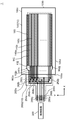
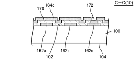
図8は、図1の第3の変形例を示す図である。図9は、図8に示した基板100の一部分の拡大平面図である。図10は、図9のC-C断面図である。図8、図9及び図10に示す例は、以下の点を除いて、図1に示した例と同様である。
図8から図10を用いて、発光装置1の概要を説明する。発光装置1は、複数の第1接続配線162a、複数の第2接続配線162b及び複数の第3接続配線162cを含んでいる。複数の第1接続配線162a、複数の第2接続配線162b及び複数の第3接続配線162cは、一緒に並んでいる。発光装置1は、第1配線164a、第2配線164b及び第3配線164cを含んでいる。図10に示すように、第1接続配線162a、第2接続配線162b、第3接続配線162c、第1配線164a、第2配線164b及び第3配線164cは、基板100の第1面102上に位置している。第1配線164aは、複数の第1接続配線162aに接続している。第2配線164bは、複数の第2接続配線162bに接続している。第3配線164cは、複数の第3接続配線162cに接続している。
上述した構成によれば、複数の発光部にそれぞれ接続する複数の接続配線を狭ピッチで並べることができる。具体的には、上述した構成においては、複数の発光部(例えば、複数の第1発光部140a)にそれぞれ接続する複数の接続配線(例えば、複数の第1接続配線162a)を互いに接続させるための配線(例えば、第1配線164a)を基板100の第1面102上に設けることができる。したがって、複数の接続配線を基板100の外部(例えば、配線基板200)まで引き出す必要がない。基板100の外部(例えば、配線基板200)では、複数の接続配線(例えば、図1に示した複数の第1接続配線262a)を狭ピッチで並べることが困難な場合がある。これに対して、基板100の第1面102上においては、各発光部を形成するための微細加工技術(例えば、リソグラフィによるパターニング又はマスクを用いた蒸着によるパターニング)を用いて複数の接続配線を狭ピッチで並べることができる。このようにして、複数の発光部にそれぞれ接続する複数の接続配線を狭ピッチで並べることができる。
図8から図10に示す例では、発光装置1は、3つの群の発光部、すなわち、複数の第1発光部140a、複数の第2発光部140b及び複数の第3発光部140cを含んでいるが、他の例において、発光装置1は、2つの群のみの発光部、例えば、複数の第1発光部140a及び複数の第3発光部140cのみを含んでいてもよいし、発光装置1は、少なくとも1つの群の発光部及び1つの発光部を有していてもよい。発光装置1が1つの群のみの発光部及び2つの群のみの発光部を含んでいる場合であっても、上述したように、複数の発光部にそれぞれ接続する複数の接続配線を狭ピッチで並べることができる。
図8から図10に示す例では、複数の第1発光部140aの第1色、複数の第2発光部140bの第2色及び複数の第3発光部140cの第3色は、互いに異なり、それぞれ、例えば、赤色(R)、緑色(G)及び青色(B)であるが、他の例において、複数の第1発光部140aの第1色、複数の第2発光部140bの第2色及び複数の第3発光部140cの第3色のうちの少なくとも2色は、同じ色であってもよい。例えば、複数の第1発光部140a及び複数の第2発光部140bの双方が第1色の光を発してもよい。
図8から図10に示す例では、複数の第1接続配線162a、複数の第2接続配線162b及び複数の第3接続配線162cは、規則的な順に、すなわち、第1接続配線162a、第2接続配線162b及び第3接続配線162cの順に繰り返し並んでいる。他の例において、複数の第1接続配線162a、複数の第2接続配線162b及び複数の第3接続配線162cは、少なくとも一部分において不規則な順に並んでいてもよい。
図8を用いて、発光装置1の詳細を説明する。
複数の第1発光部140a、複数の第2発光部140b及び複数の第3発光部140cは、図2に示したように、互いに離間した複数の第1電極110を含んでいてもよい。この場合、第1接続配線162a、第2接続配線162b及び第3接続配線162cのそれぞれは、第1電極110と一体となって形成されていてもよい。この場合、複数の第1接続配線162a、複数の第2接続配線162b、複数の第3接続配線162c及び複数の第1電極110は、例えば、導電層のパターニングによって、同時に形成させることができる。
複数の第1発光部140a、複数の第2発光部140b及び複数の第3発光部140cは、図3に示したように、互いに離間した複数の第2電極130を含んでいてもよい。この場合、第1接続配線162a、第2接続配線162b及び第3接続配線162cのそれぞれは、第2電極130と一体となって形成されていてもよい。この場合、複数の第1接続配線162a、複数の第2接続配線162b、複数の第3接続配線162c及び複数の第2電極130は、例えば、マスクを用いた蒸着によって、同時に形成させることができる。
基板100には、第1配線164a、第2配線164b及び第3配線164cと同様にして、配線164gが設けられている。配線164gの一端は、電極160の一端に接続しており、配線164gのもう一端は、電極160のもう一端に接続している。
配線基板200の第1端子266aは、基板100の第1配線164aに接続しており、配線基板200の第2端子266bは、基板100の第2配線164bに接続しており、配線基板200の第3端子266cは、基板100の第3配線164cに接続しており、配線基板200の端子266gは、基板100の配線164gに接続している。
図9及び図10を用いて、発光装置1の詳細を説明する。
発光装置1は、絶縁層170を含んでいる。絶縁層170は、基板100の第1面102上に位置しており、第1接続配線162aの少なくとも一部分、第2接続配線162bの少なくとも一部分及び第3接続配線162cの少なくとも一部分を覆っている。絶縁層170は、図2及び図3に示した絶縁層150と一体として形成されていてもよい。
第1配線164a、第2配線164b及び第3配線164cは、絶縁層170上に位置している。第1配線164aは、第1接続配線162aと交差する方向(図内のX方向)に延伸しており、第1接続配線162aの一領域と重なっている。第2配線164bは、第2接続配線162bと交差する方向(図内のX方向)に延伸しており、第1接続配線162aの一領域及び第2接続配線162bの一領域と重なっている。第3配線164cは、第3接続配線162cと交差する方向(図内のX方向)に延伸しており、第1接続配線162aの一領域、第2接続配線162bの一領域及び第3接続配線162cの一領域と重なっている。
絶縁層170は、第1配線164a及び第1接続配線162aの重なり領域において、第1配線164a及び第1接続配線162aを相互に接続するための開口172を有している。したがって、第1配線164a及び第1接続配線162aの相互接続を実現することができる。
絶縁層170は、第2配線164b及び第2接続配線162bの重なり領域において、第2配線164b及び第2接続配線162bを相互に接続するための開口172を有しており、第2配線164b及び第1接続配線162aの重なり領域において、第2配線164b及び第1接続配線162aを互いに隔てている。したがって、第2配線164b及び第2接続配線162bの相互接続を実現するとともに、第2配線164b及び第1接続配線162aの相互接続を防ぐことができる。
絶縁層170は、第3配線164c及び第3接続配線162cの重なり領域において、第3配線164c及び第3接続配線162cを相互に接続するための開口172を有しており、第3配線164c及び第2接続配線162bの重なり領域において、第3配線164c及び第2接続配線162bを互いに隔てており、第3配線164c及び第1接続配線162aの重なり領域において、第3配線164c及び第1接続配線162aを互いに隔てている。したがって、第3配線164c及び第3接続配線162cの相互接続を実現するとともに、第3配線164c及び第2接続配線162bの相互接続及び第3配線164c及び第1接続配線162aの相互接続を防ぐことができる。
図11は、図1の第4の変形例を示す図である。図11に示す例は、以下の点を除いて、図8に示した例と同様である。
発光装置1は、複数の第4発光部140d、複数の第4接続配線162d及び第4配線164dを含んでいる。複数の第4発光部140dは、複数の第1発光部140a、複数の第2発光部140b、複数の第3発光部140cと同様にして、基板100の第1面102(図2又は図3)上に位置している。複数の第4接続配線162dは、複数の第4発光部140dにそれぞれ接続している。複数の第4接続配線162dは、複数の第1接続配線162a、複数の第2接続配線162b及び第3接続配線162cと一緒に並んでいる。第4接続配線162d及び第4配線164dは、第1接続配線162a、第2接続配線162b、第3接続配線162c、第1配線164a、第2配線164b及び第3配線164cと同様にして、基板100の第1面102(図10)上に位置している。第4配線164dは、複数の第4接続配線162dに接続している。配線基板200の第4端子266dは、基板100の第4配線164dに接続している。
一例において、複数の第1発光部140aの第1色、複数の第2発光部140bの第2色、複数の第3発光部140cの第3色及び複数の第4発光部140dの第4色は、それぞれ、赤色(R)、緑色(G)、青色(B)及び黄色(Y)にすることができる。他の例において、複数の第1発光部140aの第1色、複数の第2発光部140bの第2色、複数の第3発光部140cの第3色及び複数の第4発光部140dの第4色は、それぞれ、赤色(R)、緑色(G)、青色(B)及び白色(W)にすることができる。
図11に示す例では、複数の第1接続配線162a、複数の第2接続配線162b、複数の第3接続配線162c及び複数の第4接続配線162dは、規則的な順に、すなわち、第1接続配線162a、第2接続配線162b、第3接続配線162c及び第4接続配線162dの順に繰り返し並んでいる。他の例において、複数の第1接続配線162a、複数の第2接続配線162b、複数の第3接続配線162c及び複数の第4接続配線162dは、少なくとも一部分において不規則な順に並んでいてもよい。
図11に示す例においても、複数の発光部にそれぞれ接続する複数の接続配線を狭ピッチで並べることができる。
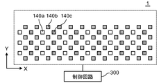
図12は、複数の第1発光部140a、複数の第2発光部140b及び複数の第3発光部140cのレイアウトの第1の変形例を説明するための図である。
複数の第1発光部140a、複数の第2発光部140b及び複数の第3発光部140cは、ドットマトリクス状に配置されていてもよい。
図13は、複数の第1発光部140a、複数の第2発光部140b及び複数の第3発光部140cのレイアウトの第2の変形例を説明するための図である。
複数の第1発光部140a、複数の第2発光部140b及び複数の第3発光部140cは、ペンタイルマトリクス状に配置されていてもよい。
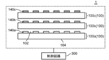
図14は、複数の第1発光部140a、複数の第2発光部140b及び複数の第3発光部140cのレイアウトの第3の変形例を説明するための図である。
複数の第2発光部140bのそれぞれは、複数のセパレータ182のそれぞれを挟んで、複数の第1発光部140aのそれぞれ上に積み重ねられており、複数の第3発光部140cは、複数のセパレータ184のそれぞれを挟んで、複数の第3発光部140cのそれぞれ上に積み重ねられている。セパレータ182によって、第1発光部140a及び第2発光部140bは、電気的に互いに絶縁されており、セパレータ184によって第2発光部140b及び第3発光部140cは、電気的に互いに絶縁されている。したがって、図1に示した例と同様にして、制御回路300は、第1タイミングにおいて、複数の第1発光部140aを発光させ、第2タイミングにおいて、複数の第2発光部140bを発光させ、第3タイミングにおいて、複数の第3発光部140cを発光させることができる。
基板100の第2面104から光が出射される場合、各第1発光部140a、各セパレータ182、各第2発光部140b及び各セパレータ184は、透光性を有している。したがって、各第2発光部140bから発せられた光は、セパレータ182及び第1発光部140aを透過して基板100の第2面104から出射されることができ、各第3発光部140cから発せられた光は、セパレータ184、第2発光部140b、セパレータ182及び第1発光部140aを透過して基板100の第2面104から出射されることができる。
基板100の第2面104の反対側から光が出射される場合、セパレータ182、第2発光部140b、セパレータ184及び第3発光部140cは、透光性を有している。したがって、各第1発光部140aから発せられた光は、セパレータ182、第2発光部140b、セパレータ184及び第3発光部140cを透過して基板100の第2面104の反対側から出射されることができ、各第2発光部140bから発せられた光は、セパレータ184及び第3発光部140cを透過して基板100の第2面104の反対側から出射されることができる。
図14に示す例では、互いに分離した複数の第1発光部140a、互いに分離した複数の第2発光部140b及び互いに分離した複数の第3発光部140cが基板100の第1面102に沿って並んでいるが、他の例において、単一の第1発光部140a、単一の第2発光部140b及び単一の第3発光部140cが基板100の第1面102に沿って広がっていてもよい。当該他の例によれば、各発光部に接続する配線を簡素化することができ、各発光部の発光量を増加させることができ、各発光部の塗布プロセスを簡素化することができる。
図15は、複数の第1発光部140a、複数の第2発光部140b及び複数の第3発光部140cのレイアウトの第4の変形例を説明するための図である。
発光装置1は、複数の基板100、すなわち、第1基板100a、第2基板100b及び第3基板100cを含んでいる。第2基板100bは、第1基板100a上に積み重ねられており、第3基板100cは、第2基板100b上に積み重ねられている。第1基板100aの第1面102上には、複数の第1発光部140aが位置している。第2基板100bの第1面102上には、複数の第2発光部140bが位置している。第3基板100cの第1面102上には、複数の第3発光部140cが位置している。図1に示した例と同様にして、制御回路300は、第1タイミングにおいて、複数の第1発光部140aを発光させ、第2タイミングにおいて、複数の第2発光部140bを発光させ、第3タイミングにおいて、複数の第3発光部140cを発光させることができる。
第1基板100aの第2面104から光が出射される場合、第1発光部140a及び第2発光部140bは透光性を有している。したがって、各第3発光部140cから発せられた光は、第2発光部140b、第2基板100b、第1発光部140a及び第1基板100aを透過して基板100の第2面104から出射されることができ、各第2発光部140bから発せられた光は、第1発光部140a及び第1基板100aを透過して基板100の第2面104から出射されることができる。
第1基板100aの第2面104の反対側(第3基板100cの第1面102側)から光が出射される場合、第2発光部140b及び第3発光部140cは、透光性を有している。したがって、各第1発光部140aから発せられた光は、第2基板100b、第2発光部140b、第3基板100c及び第3発光部140cを透過して第1基板100aの第2面104の反対側(第3基板100cの第1面102側)から出射されることができ、各第2発光部140bから発せられた光は、第3基板100c及び第3発光部140cを透過して第1基板100aの第2面104の反対側(第3基板100cの第1面102側)から出射されることができる。
図15に示す例では、互いに分離した複数の第1発光部140a、互いに分離した複数の第2発光部140b及び互いに分離した複数の第3発光部140cが第1基板100aの第1面102、第2基板100bの第1面102及び第3基板100cの第1面102に沿ってそれぞれ並んでいるが、他の例において、単一の第1発光部140a、単一の第2発光部140b及び単一の第3発光部140cが第1基板100aの第1面102、第2基板100bの第1面102及び第3基板100cの第1面102に沿ってそれぞれ広がっていてもよい。当該他の例によれば、各発光部に接続する配線を簡素化することができ、各発光部の発光量を増加させることができ、各発光部の塗布プロセスを簡素化することができる。
(実施例1)
図16は、実施例1に係る発光モジュール2を示す図である。
図16は、実施例1に係る発光モジュール2を示す図である。
図16を用いて、発光モジュール2について説明する。発光モジュール2は、発光板10及び反射部材20を含んでいる。発光板10は、光照射面12を有している。反射部材20は、反射面22を有している。反射面22は、発光板10の光照射面12から発せられた光を対象物30の対象面32に向けて反射するためのものである。光照射面12の第1領域12aの配光分布におけるピーク光度の光(光L1)は、反射面22の第1領域22aを経由して対象面32の第1領域32aに送られる。光照射面12の第2領域12bの配光分布におけるピーク光度の光(光L2)は、反射面22の第2領域22bを経由して対象面32の第2領域32bに送られる。光照射面12の第1領域12aから反射面22の第1領域22aを経由して対象面32の第1領域32aまでの光学的距離は、光照射面12の第2領域12bから反射面22の第2領域22bを経由して対象面32の第2領域32bまでの光学的距離より大きくなっている。光L1の光度は、光L2の光度より大きくなっている。
上述した構成によれば、対象面32の輝度分布のばらつきを抑えることができる。具体的には、上述した構成においては、光L1の光学的距離が光L2の光学的距離より大きくなっている。仮に、光L1の光度が光L2の光度と等しいと、光L1の光路における光L1の減衰が光L2の光路における光L2の減衰より大きくなり、対象面32の第1領域32aにおける輝度が対象面32の第2領域32bにおける輝度より小さくなり得る。これに対して、上述した構成においては、光L1の光度は、光L2の光度より大きくなっており、具体的には、対象面32の第1領域32aにおける輝度が対象面32の第2領域32bにおける輝度と実質的に等しくなるように、光L2の光度より大きくなっている。このようにして、対象面32の輝度分布のばらつきを抑えることができる。この他に、反射部材20及び対象物30の配置並びに反射部材20の形状の設計自由度を向上させることができる。
図16に示す例では、光L1は、光照射面12の第1領域12aの法線方向に沿って出射されており、光L2は、光照射面12の第2領域12bの法線方向に沿って出射されている。他の例において、光L1、すなわち、光照射面12の第1領域12aの配光分布におけるピーク光度の光は、光照射面12の第1領域12aの法線方向から傾いた方向に沿って出射されてもよい。一例において、発光板10に含まれる有機層120(図2又は図3)の各層の厚さを調節することで、配光分布におけるピーク光度の向きを調節することができる。光L2についても同様である。
図16に示す例では、光L1は、光L2と実質的に平行に出射されている。具体的には、発光板10の光照射面12は、実質的に平坦になっている。図16に示す例では、対象面32の輝度のばらつきを抑えるために光照射面12の光度分布を調節している。つまり、発光板10を湾曲させることなく、対象面32の輝度のばらつきを抑えることができる。
図16に示す例において、対象物30の対象面32は、実質的に平坦になっている。
次に、発光モジュール2の用途の第1例を説明する。この例において、発光モジュール2は、反射型LCD、より具体的には、例えば、電子ビューファインダ(EVF)に用いられることができる。
この例において、反射部材20は、偏光ビームスプリッタ(PBS)であり、対象物30は、反射型LCD素子、より具体的にはLCOS((Liquid Crystal On Silicon))である。
発光モジュール2は、以下のようにして所望の画像を表示する。発光板10の光照射面12から照射された光のS偏光を反射部材20によって対象物30に向けて反射させる。対象物30の対象面32の一の領域は、反射部材20から反射されたS偏光の偏光方向を変えないまま、このS偏光を反射部材20に向けて戻し、対象物30の対象面32の他の一の領域は、反射部材20から反射されたS偏光をP偏光に変換して、このP偏光を反射部材20に向けて戻す。反射部材20に向けて戻されたS偏光は反射部材20を透過しない一方で、反射部材20に向けて戻されたP偏光は反射部材20を透過する。対象物30の上述した一の領域及び他の一領域を対象物30内の回路によって制御することで、所望の画像を表示することができる。
この例において、発光板10は、実施形態を用いて説明したように、FSCディスプレイの光源として機能させることができる。一例において、実施形態と同様にして、発光板10は、第1タイミングにおいて第1色(例えば、赤色(R))の光を発し、第2タイミングにおいて第2色(例えば、緑色(G))の光を発し、第3タイミングにおいて第3色(例えば、青色(B))の光を発し、対象物30(例えば、LCOS)は、第1タイミングにおいて、対象面32に照射される第1色の光の一部を選択して第1画像を生成し、第2タイミングにおいて、対象面32に照射される第2色の光の一部を選択して第2画像を生成し、第3タイミングにおいて、対象面32に照射される第3色の光の一部を選択して第3画像を生成する。第1画像、第2画像及び第3画像の合成によって、一つのカラー画像を生成することができる。
次に、発光モジュール2の用途の第2例を説明する。この例において、発光モジュール2は、ヘッドアップディスプレイ(HUD)に用いられることができる。このHUDは、例えば自動車に実装することができる。
この例において、反射部材20は、ミラーであり、対象物30は、画像を投影するための透明ディスプレイであり、HUDが自動車に実装される場合は、例えばフロントガラスにすることができる。
図17は、図16に示した発光板10の光照射面12のレイアウトの一例を示す図である。
実施形態と同様にして、発光板10は、複数の発光部140(複数の第1発光部140a、複数の第2発光部140b及び複数の第3発光部140c)を含んでいる。複数の第1発光部140a、複数の第2発光部140b及び複数の第3発光部140cは、一緒に繰り返し並んでいる。
光照射面12の第1領域12aの面積は、光照射面12の第2領域12bの面積と等しくなっている。第1領域12aに占める発光部140の面積は、第2領域12bに占める発光部140の面積より大きくなっている。したがって、光L1(第1領域12aから照射される光(図16))の光度を光L2(第2領域12bから照射される光(図17))の光度より大きくすることができる。
図17に示す例では、各発光部140の幅が第1領域12aから第2領域12bに向かうにつれて狭くなっている。したがって、光照射面12は、第1領域12aから第2領域12bに向けて光度が減少する光度分布を有している。
(実施例2)
図18は、実施例2に係る発光モジュール2を示す図である。実施例2に係る発光モジュール2は、以下の点を除いて、実施例1に係る発光モジュール2と同様である。
図18は、実施例2に係る発光モジュール2を示す図である。実施例2に係る発光モジュール2は、以下の点を除いて、実施例1に係る発光モジュール2と同様である。
光L1の光度は、光L2の光度と実質的に等しくなっている。反射面22の第1領域22aにおける法線方向は、反射面22の第2領域22bにおける法線方向と異なっている。光照射面12の第1領域12aから反射面22の第1領域22aを経由して対象面32の第1領域32aまでの光学的距離は、光照射面12の第2領域12bから反射面22の第2領域22bを経由して対象面32の第2領域32bまでの光学的距離と実質的に等しくなっている。図18に示す例では、光L1の光学的距離を光L2の光学的距離と実質的に等しくするため、光照射面12の第1領域12aから反射面22の第1領域22aを経由して対象面32の第1領域32aまでの物理的距離は、光照射面12の第2領域12bから反射面22の第2領域22bを経由して対象面32の第2領域32bまでの物理的距離と実質的に等しくなっている。
上述した構成によれば、対象面32の輝度分布のばらつきを抑えることができる。具体的には、上述した構成においては、反射面22の第1領域22aにおける法線方向が反射面22の第2領域22bにおける法線方向と異なっており、光L1の光度が光L2の光度と実質的に等しくなっている。仮に、光L1及び光L2を互いに平行に照射すると、光L1の光学的距離が光L2の光学的距離と異なるようになり、対象面32の第1領域32aにおける輝度が対象面32の第2領域32bにおける輝度と異なり得るようになる。これに対して、上述した構成においては、光L1の光学的距離は、光L2の光学的距離と実質的に等しくなっている。このようにして、対象面32の輝度分布のばらつきを抑えることができる。この他に、反射部材20及び対象物30の配置並びに反射部材20の形状の設計自由度を向上させることができる。
図18に示す例において、反射部材20の反射面22は、湾曲している。したがって、反射部材20の反射面22の法線方向は、反射面22の領域に応じて異なっている。上述した構成によれば、反射部材20の反射面22が湾曲している場合であっても、対象面32の輝度分布のばらつきを抑えることができる。
さらに、上述した構成によれば、反射部材20の反射面22が湾曲しておらず、互いに異なる法線方向を有する複数の平坦面を有する場合であっても、対象面32の輝度分布のばらつきを抑えることができる。
図18に示す例では、光L1についての物理的距離を光L2についての物理的距離と等しくするため、光L1は、光L2とは異なる方向に出射されている。具体的には、光L1は、光照射面12の第1領域12aにおける法線方向に沿って出射され、光L2は、光照射面12の第1領域12aにおける法線方向に沿って出射され、光照射面12は、湾曲している。
(実施例3)
図19は、実施例3に係る発光モジュール2を示す図である。実施例3に係る発光モジュール2は、以下の点を除いて、実施例2に係る発光モジュール2と同様である。
図19は、実施例3に係る発光モジュール2を示す図である。実施例3に係る発光モジュール2は、以下の点を除いて、実施例2に係る発光モジュール2と同様である。
光照射面12の第1領域12aから反射面22の第1領域22aを経由して対象面32の第1領域32aまでの物理的距離は、光照射面12の第2領域12bから反射面22の第2領域22bを経由して対象面32の第2領域32bまでの物理的距離より大きくなっている。光照射面12の第2領域12bから反射面22の第2領域22bを経由して対象面32の第2領域32bまでの光学的経路は、第1屈折率を有する第1経路部分(高屈折率領域40以外の部分)及び第1屈折率より大きい第2屈折率を有する第2経路部分(高屈折率領域40)を含んでいる。
上述した構成によれば、光L2についての第2経路部分(高屈折率領域40)の長さ及び屈折率を調節することで、光L1の光学的距離を光L2の光学的距離と実質的に等しくさせることができる。したがって、対象面32の輝度分布のばらつきを抑えることができる。
図19に示す例において、第1経路部分(高屈折率領域40以外の部分)は、例えば、空気にすることができ、第2経路部分(高屈折率領域40)は、例えば、空気よりも高い屈折率を有する媒質(例えば、ガラス、水又は樹脂)にすることができる。
図19に示す例では、光L1は、光L2と実質的に平行に出射されている。具体的には、発光板10の光照射面12は、実質的に平坦になっており、光L1は、光照射面12の第1領域12aにおける法線方向に沿って出射され、光L2は、光照射面12の第1領域12aにおける法線方向に沿って出射されている。図19に示す例では、対象面32の輝度のばらつきを抑えるために高屈折率領域40を設けている。つまり、発光板10を湾曲させることなく、対象面32の輝度のばらつきを抑えることができる。
以上、図面を参照して実施形態及び実施例について述べたが、これらは本発明の例示であり、上記以外の様々な構成を採用することもできる。
以下、参考形態の例を付記する。
(参考形態1)
近年、新規なディスプレイとして、フィールドシーケンシャルカラー(FSC)ディスプレイ(例えば、FSC液晶ディスプレイ(LCD))が開発されている。本発明者は、OLEDをFSCディスプレイの光源として機能させることを検討した。
近年、新規なディスプレイとして、フィールドシーケンシャルカラー(FSC)ディスプレイ(例えば、FSC液晶ディスプレイ(LCD))が開発されている。本発明者は、OLEDをFSCディスプレイの光源として機能させることを検討した。
本発明が解決しようとする課題としては、OLEDをFSCディスプレイの光源として機能させることが一例として挙げられる。
1-1. 第1色の光を発する有機EL素子を含む複数の第1発光部と、
前記第1色と異なる第2色の光を発する有機EL素子を含み、前記複数の第1発光部とそれぞれ隣り合う複数の第2発光部と、
制御回路と、
を含み、
前記制御回路は、
第1タイミングにおいて、前記複数の第1発光部を発光させる一方で前記複数の第2発光部を発光させず、
第2タイミングにおいて、前記複数の第2発光部を発光させる一方で前記複数の第1発光部を発光させない、発光装置。
1-2. 1-1.に記載の発光装置において、
第1面を有する基板をさらに含み、
前記複数の第1発光部及び前記複数の第2発光部は、前記基板の前記第1面に沿って並んでいる、発光装置。
1-3. 1-2.に記載の発光装置において、
前記第1色及び前記第2色のいずれとも異なる第3色の光を発する有機EL素子を含み、前記基板の前記第1面に沿って、前記複数の第1発光部及び前記複数の第2発光部と一緒に並ぶ複数の第3発光部を含み、
前記制御回路は、
前記第1タイミング及び前記第2タイミングにおいて、前記複数の第3発光部を発光させず、
第3タイミングにおいて、前記複数の第3発光部を発光させる一方で前記複数の第1発光部及び前記複数の第2発光部を発光させない、発光装置。
1-4. 1-3.に記載の発光装置において、
前記複数の第1発光部、前記複数の第2発光部及び前記複数の第3発光部は、前記基板の前記第1面に沿って、第1発光部、第2発光部及び第3発光部の順に繰り返し並んでいる、発光装置。
1-5. 1-3.又は1-4.に記載の発光装置において、
前記第1色は、赤色であり、
前記第2色は、緑色であり、
前記第3色は、青色である、発光装置。
1-6. 1-3.に記載の発光装置において、
前記第1色、前記第2色及び前記第3色のいずれとも異なる第4色の光を発する有機EL素子を含み、前記基板の前記第1面に沿って、前記複数の第1発光部、前記複数の第2発光部及び前記複数の第3発光部と一緒に並ぶ複数の第4発光部をさらに含み、
前記制御回路は、
前記第1タイミング、前記第2タイミング及び前記第3タイミングにおいて、前記複数の第4発光部を発光させず、
第4タイミングにおいて、前記複数の第4発光部を発光させる一方で前記複数の第1発光部、前記複数の第2発光部及び前記複数の第3発光部を発光させない、発光装置。
1-7. 1-6.に記載の発光装置において、
前記複数の第1発光部、前記複数の第2発光部、前記複数の第3発光部及び前記複数の第4発光部は、前記基板の前記第1面に沿って、第1発光部、第2発光部、第3発光部及び第4発光部の順に繰り返し並んでいる、発光装置。
1-8. 1-6.又は1-7.に記載の発光装置において、
前記第1色は、赤色であり、
前記第2色は、緑色であり、
前記第3色は、青色であり、
前記第4色は、黄色である、発光装置。
1-9. 1-1.から1-8までのいずれか一つに記載の発光装置において、
前記複数の第1発光部にそれぞれ接続する複数の第1接続配線と、
前記複数の第1接続配線に接続する第1配線と、
前記第1配線に接続する第1端子と、
前記複数の第2発光部にそれぞれ接続する複数の第2接続配線と、
前記複数の第2接続配線に接続する第2配線と、
前記第2配線に接続する第2端子と、
をさらに含み、
前記制御回路は、
前記第1タイミングにおいて、前記複数の第1発光部を発光させるための電圧を前記第1端子に印加し、
前記第2タイミングにおいて、前記複数の第2発光部を発光させるための電圧を前記第2端子に印加する、発光装置。
1-10. 1-1.から1-9までのいずれか一つに記載の発光装置において、
前記複数の第1発光部は、互いに離間した複数の第1電極をそれぞれ含み、
前記複数の第2発光部は、互いに離間した複数の第1電極をそれぞれ含み、
前記複数の第1発光部及び前記複数の第2発光部は、前記複数の第1発光部の前記複数の第1電極及び前記複数の第2発光部の前記複数の第1電極を覆う共通の第2電極を含む、発光装置。
1-11. 1-1.に記載の発光装置において、
前記複数の第2発光部のそれぞれは、前記複数の第1発光部のそれぞれ上に積み重ねられている、発光装置。
1-12. 1-1.に記載の発光装置において、
前記複数の第1発光部が位置する第1基板と、
前記複数の第2発光部が位置する第2基板と、
をさらに含み、
前記第2基板は、前記第1基板上に積み重ねられている、発光装置。
1-13. 発光装置の制御方法であって、
第1色の光を発する有機EL素子を含む複数の第1発光部と、
前記第1色と異なる第2色の光を発する有機EL素子を含み、前記複数の第1発光部とそれぞれ隣り合う複数の第2発光部と、
を準備して、
第1タイミングにおいて、前記複数の第1発光部を発光させる一方で前記複数の第2発光部を発光させず、
前記第1タイミングと異なる第2タイミングにおいて、前記複数の第2発光部を発光させる一方で前記複数の第1発光部を発光させない、発光装置の制御方法。
前記第1色と異なる第2色の光を発する有機EL素子を含み、前記複数の第1発光部とそれぞれ隣り合う複数の第2発光部と、
制御回路と、
を含み、
前記制御回路は、
第1タイミングにおいて、前記複数の第1発光部を発光させる一方で前記複数の第2発光部を発光させず、
第2タイミングにおいて、前記複数の第2発光部を発光させる一方で前記複数の第1発光部を発光させない、発光装置。
1-2. 1-1.に記載の発光装置において、
第1面を有する基板をさらに含み、
前記複数の第1発光部及び前記複数の第2発光部は、前記基板の前記第1面に沿って並んでいる、発光装置。
1-3. 1-2.に記載の発光装置において、
前記第1色及び前記第2色のいずれとも異なる第3色の光を発する有機EL素子を含み、前記基板の前記第1面に沿って、前記複数の第1発光部及び前記複数の第2発光部と一緒に並ぶ複数の第3発光部を含み、
前記制御回路は、
前記第1タイミング及び前記第2タイミングにおいて、前記複数の第3発光部を発光させず、
第3タイミングにおいて、前記複数の第3発光部を発光させる一方で前記複数の第1発光部及び前記複数の第2発光部を発光させない、発光装置。
1-4. 1-3.に記載の発光装置において、
前記複数の第1発光部、前記複数の第2発光部及び前記複数の第3発光部は、前記基板の前記第1面に沿って、第1発光部、第2発光部及び第3発光部の順に繰り返し並んでいる、発光装置。
1-5. 1-3.又は1-4.に記載の発光装置において、
前記第1色は、赤色であり、
前記第2色は、緑色であり、
前記第3色は、青色である、発光装置。
1-6. 1-3.に記載の発光装置において、
前記第1色、前記第2色及び前記第3色のいずれとも異なる第4色の光を発する有機EL素子を含み、前記基板の前記第1面に沿って、前記複数の第1発光部、前記複数の第2発光部及び前記複数の第3発光部と一緒に並ぶ複数の第4発光部をさらに含み、
前記制御回路は、
前記第1タイミング、前記第2タイミング及び前記第3タイミングにおいて、前記複数の第4発光部を発光させず、
第4タイミングにおいて、前記複数の第4発光部を発光させる一方で前記複数の第1発光部、前記複数の第2発光部及び前記複数の第3発光部を発光させない、発光装置。
1-7. 1-6.に記載の発光装置において、
前記複数の第1発光部、前記複数の第2発光部、前記複数の第3発光部及び前記複数の第4発光部は、前記基板の前記第1面に沿って、第1発光部、第2発光部、第3発光部及び第4発光部の順に繰り返し並んでいる、発光装置。
1-8. 1-6.又は1-7.に記載の発光装置において、
前記第1色は、赤色であり、
前記第2色は、緑色であり、
前記第3色は、青色であり、
前記第4色は、黄色である、発光装置。
1-9. 1-1.から1-8までのいずれか一つに記載の発光装置において、
前記複数の第1発光部にそれぞれ接続する複数の第1接続配線と、
前記複数の第1接続配線に接続する第1配線と、
前記第1配線に接続する第1端子と、
前記複数の第2発光部にそれぞれ接続する複数の第2接続配線と、
前記複数の第2接続配線に接続する第2配線と、
前記第2配線に接続する第2端子と、
をさらに含み、
前記制御回路は、
前記第1タイミングにおいて、前記複数の第1発光部を発光させるための電圧を前記第1端子に印加し、
前記第2タイミングにおいて、前記複数の第2発光部を発光させるための電圧を前記第2端子に印加する、発光装置。
1-10. 1-1.から1-9までのいずれか一つに記載の発光装置において、
前記複数の第1発光部は、互いに離間した複数の第1電極をそれぞれ含み、
前記複数の第2発光部は、互いに離間した複数の第1電極をそれぞれ含み、
前記複数の第1発光部及び前記複数の第2発光部は、前記複数の第1発光部の前記複数の第1電極及び前記複数の第2発光部の前記複数の第1電極を覆う共通の第2電極を含む、発光装置。
1-11. 1-1.に記載の発光装置において、
前記複数の第2発光部のそれぞれは、前記複数の第1発光部のそれぞれ上に積み重ねられている、発光装置。
1-12. 1-1.に記載の発光装置において、
前記複数の第1発光部が位置する第1基板と、
前記複数の第2発光部が位置する第2基板と、
をさらに含み、
前記第2基板は、前記第1基板上に積み重ねられている、発光装置。
1-13. 発光装置の制御方法であって、
第1色の光を発する有機EL素子を含む複数の第1発光部と、
前記第1色と異なる第2色の光を発する有機EL素子を含み、前記複数の第1発光部とそれぞれ隣り合う複数の第2発光部と、
を準備して、
第1タイミングにおいて、前記複数の第1発光部を発光させる一方で前記複数の第2発光部を発光させず、
前記第1タイミングと異なる第2タイミングにおいて、前記複数の第2発光部を発光させる一方で前記複数の第1発光部を発光させない、発光装置の制御方法。
(参考形態2)
OLEDでは、複数の発光部にそれぞれ接続された複数の接続配線に電圧を供給するため、これら複数の接続配線に共通の配線を接続させることがある。本発明者は、OLEDを構成する基板の外側に位置する素子(例えば、フレキシブルプリント回路(FPC))において、共通の配線を複数の接続配線に接続させた場合、素子の構造によっては、素子内において複数の接続配線をある程度広いピッチで並べる必要があることを見出した。
OLEDでは、複数の発光部にそれぞれ接続された複数の接続配線に電圧を供給するため、これら複数の接続配線に共通の配線を接続させることがある。本発明者は、OLEDを構成する基板の外側に位置する素子(例えば、フレキシブルプリント回路(FPC))において、共通の配線を複数の接続配線に接続させた場合、素子の構造によっては、素子内において複数の接続配線をある程度広いピッチで並べる必要があることを見出した。
本発明が解決しようとする課題としては、複数の発光部にそれぞれ接続する複数の接続配線を狭ピッチで並べることが一例として挙げられる。
2-1. 第1面を有する基板と、
前記基板の前記第1面上に位置し、第1色の光を発する有機EL素子を含む複数の第1発光部と、
前記基板の前記第1面上に位置し、前記複数の第1発光部にそれぞれ接続する複数の第1接続配線と、
前記基板の前記第1面上に位置し、前記複数の第1接続配線に接続する第1配線と、
前記基板の前記第1面上に位置し、前記第1色又は第2色の光を発する有機EL素子を含む複数の第2発光部と、
前記基板の前記第1面上に位置し、前記複数の第2発光部にそれぞれ接続し、前記複数の第1接続配線と一緒に並ぶ複数の第2接続配線と、
前記基板の前記第1面上に位置し、前記複数の第2接続配線に接続する第2配線と、
を含む発光装置。
2-2. 2-1.に記載の発光装置において、
前記基板の前記第1面上に位置し、前記複数の第1接続配線のそれぞれの少なくとも一部分及び前記複数の第2接続配線のそれぞれの少なくとも一部分を覆う絶縁層をさらに含み、
前記第1配線は、前記絶縁層上に位置しており、前記第1接続配線の一領域と重なっており、
前記第2配線は、前記絶縁層上に位置しており、前記第1接続配線の一領域及び前記第2接続配線の一領域と重なっており、
前記絶縁層は、
前記第1配線及び前記第1接続配線の重なり領域において、前記第1配線及び前記第1接続配線を相互に接続するための開口を有し、
前記第2配線及び前記第2接続配線の重なり領域において、前記第2配線及び前記第2接続配線を相互に接続するための開口を有し、
前記第2配線及び前記第1接続配線の重なり領域において、前記第2配線及び前記第1接続配線を互いに隔てている、発光装置。
2-3. 2-1.又は2-2.に記載の発光装置において、
前記基板の前記第1面上に位置し、第3色の光を発する有機EL素子を含む複数の第3発光部と、
前記基板の前記第1面上に位置し、前記複数の第3発光部にそれぞれ接続し、前記複数の第1接続配線及び前記複数の第2接続配線と一緒に並ぶ複数の第3接続配線と、
前記基板の前記第1面上に位置し、前記複数の第3接続配線に接続する第3配線と、
をさらに含む発光装置。
2-4. 2-3.に記載の発光装置において、
前記複数の第1接続配線、前記複数の第2接続配線及び前記複数の第3接続配線は、前記第1接続配線、前記第2接続配線及び前記第3接続配線の順に繰り返し並んでいる、発光装置。
2-5. 2-3.又は2-4.に記載の発光装置において、
前記第1色は、赤色であり、
前記第2色は、緑色であり、
前記第3色は、青色である、発光装置。
2-6. 2-3.に記載の発光装置において、
前記基板の前記第1面上に位置し、第4色の光を発する有機EL素子を含む複数の第4発光部と、
前記基板の前記第1面上に位置し、前記複数の第4発光部にそれぞれ接続し、前記複数の第1接続配線、前記複数の第2接続配線及び前記複数の第3接続配線と一緒に並ぶ複数の第4接続配線と、
前記基板の前記第1面上に位置し、前記複数の第4接続配線に接続する第4配線と、
をさらに含む発光装置。
2-7. 2-6.に記載の発光装置において、
前記複数の第1接続配線、前記複数の第2接続配線、前記複数の第3接続配線及び前記複数の第4接続配線は、前記第1接続配線、前記第2接続配線、前記第3接続配線及び前記第4接続配線の順に繰り返し並んでいる、発光装置。
2-8. 2-6.又は2-7.に記載の発光装置において、
前記第1色は、赤色であり、
前記第2色は、緑色であり、
前記第3色は、青色であり、
前記第4色は、黄色である、発光装置。
2-9. 2-1.から2-8までのいずれか一つに記載の発光装置において、
第1端子を有する回路基板をさらに含み、
前記回路基板の前記第1端子は、前記基板の前記第1配線に接続している、発光装置。
前記基板の前記第1面上に位置し、第1色の光を発する有機EL素子を含む複数の第1発光部と、
前記基板の前記第1面上に位置し、前記複数の第1発光部にそれぞれ接続する複数の第1接続配線と、
前記基板の前記第1面上に位置し、前記複数の第1接続配線に接続する第1配線と、
前記基板の前記第1面上に位置し、前記第1色又は第2色の光を発する有機EL素子を含む複数の第2発光部と、
前記基板の前記第1面上に位置し、前記複数の第2発光部にそれぞれ接続し、前記複数の第1接続配線と一緒に並ぶ複数の第2接続配線と、
前記基板の前記第1面上に位置し、前記複数の第2接続配線に接続する第2配線と、
を含む発光装置。
2-2. 2-1.に記載の発光装置において、
前記基板の前記第1面上に位置し、前記複数の第1接続配線のそれぞれの少なくとも一部分及び前記複数の第2接続配線のそれぞれの少なくとも一部分を覆う絶縁層をさらに含み、
前記第1配線は、前記絶縁層上に位置しており、前記第1接続配線の一領域と重なっており、
前記第2配線は、前記絶縁層上に位置しており、前記第1接続配線の一領域及び前記第2接続配線の一領域と重なっており、
前記絶縁層は、
前記第1配線及び前記第1接続配線の重なり領域において、前記第1配線及び前記第1接続配線を相互に接続するための開口を有し、
前記第2配線及び前記第2接続配線の重なり領域において、前記第2配線及び前記第2接続配線を相互に接続するための開口を有し、
前記第2配線及び前記第1接続配線の重なり領域において、前記第2配線及び前記第1接続配線を互いに隔てている、発光装置。
2-3. 2-1.又は2-2.に記載の発光装置において、
前記基板の前記第1面上に位置し、第3色の光を発する有機EL素子を含む複数の第3発光部と、
前記基板の前記第1面上に位置し、前記複数の第3発光部にそれぞれ接続し、前記複数の第1接続配線及び前記複数の第2接続配線と一緒に並ぶ複数の第3接続配線と、
前記基板の前記第1面上に位置し、前記複数の第3接続配線に接続する第3配線と、
をさらに含む発光装置。
2-4. 2-3.に記載の発光装置において、
前記複数の第1接続配線、前記複数の第2接続配線及び前記複数の第3接続配線は、前記第1接続配線、前記第2接続配線及び前記第3接続配線の順に繰り返し並んでいる、発光装置。
2-5. 2-3.又は2-4.に記載の発光装置において、
前記第1色は、赤色であり、
前記第2色は、緑色であり、
前記第3色は、青色である、発光装置。
2-6. 2-3.に記載の発光装置において、
前記基板の前記第1面上に位置し、第4色の光を発する有機EL素子を含む複数の第4発光部と、
前記基板の前記第1面上に位置し、前記複数の第4発光部にそれぞれ接続し、前記複数の第1接続配線、前記複数の第2接続配線及び前記複数の第3接続配線と一緒に並ぶ複数の第4接続配線と、
前記基板の前記第1面上に位置し、前記複数の第4接続配線に接続する第4配線と、
をさらに含む発光装置。
2-7. 2-6.に記載の発光装置において、
前記複数の第1接続配線、前記複数の第2接続配線、前記複数の第3接続配線及び前記複数の第4接続配線は、前記第1接続配線、前記第2接続配線、前記第3接続配線及び前記第4接続配線の順に繰り返し並んでいる、発光装置。
2-8. 2-6.又は2-7.に記載の発光装置において、
前記第1色は、赤色であり、
前記第2色は、緑色であり、
前記第3色は、青色であり、
前記第4色は、黄色である、発光装置。
2-9. 2-1.から2-8までのいずれか一つに記載の発光装置において、
第1端子を有する回路基板をさらに含み、
前記回路基板の前記第1端子は、前記基板の前記第1配線に接続している、発光装置。
この出願は、2018年5月30日に出願された日本出願特願2018-103828、2018年5月30日に出願された日本出願特願2018-103829号及び2018年5月30日に出願された日本出願特願2018-103830を基礎とする優先権を主張し、その開示の全てをここに取り込む。
Claims (10)
- 光照射面を有する発光板と、
前記発光板の前記光照射面から発せられた光を対象物の対象面に向けて反射するための反射面を有する反射部材と、
を含み、
前記光照射面の第1領域の配光分布におけるピーク光度の光は、前記反射面の第1領域を経由して前記対象面の第1領域に送られ、
前記光照射面の第2領域の配光分布におけるピーク光度の光は、前記反射面の第2領域を経由して前記対象面の第2領域に送られ、
前記光照射面の前記第1領域から前記反射面の前記第1領域を経由して前記対象面の前記第1領域までの光学的距離は、前記光照射面の前記第2領域から前記反射面の前記第2領域を経由して前記対象面の前記第2領域までの光学的距離より大きく、
前記光照射面の前記第1領域の前記配光分布における前記ピーク光度は、前記光照射面の前記第2領域の前記配光分布における前記ピーク光度より大きい、発光モジュール。 - 請求項1に記載の発光モジュールにおいて、
前記光照射面の前記第1領域の前記配光分布における前記ピーク光度の光は、前記光照射面の前記第2領域の前記配光分布における前記ピーク光度の光と実質的に平行に出射される、発光モジュール。 - 請求項1又は2に記載の発光モジュールにおいて、
前記光照射面の前記第1領域の前記配光分布における前記ピーク光度の光は、前記光照射面の前記第1領域の法線方向に沿って出射され、
前記光照射面の前記第2領域の前記配光分布における前記ピーク光度の光は、前記光照射面の前記第2領域の法線方向に沿って出射される、発光モジュール。 - 請求項1から3までのいずれか一項に記載の発光モジュールにおいて、
前記光照射面の前記第1領域の面積は、前記光照射面の前記第2領域の面積と等しく、
前記光照射面の前記第1領域に占める発光部の面積は、前記光照射面の前記第2領域に占める発光部の面積より大きい、発光モジュール。 - 光照射面を有する発光板と、
前記発光板の前記光照射面から発せられた光を対象物の対象面に向けて反射するための反射面を有する反射部材と、
を含み、
前記光照射面の第1領域の配光分布におけるピーク光度の光は、前記反射面の第1領域を経由して前記対象面の第1領域に送られ、
前記光照射面の第2領域の配光分布におけるピーク光度の光は、前記反射面の第2領域を経由して前記対象面の第2領域に送られ、
前記光照射面の前記第1領域の前記配光分布における前記ピーク光度は、前記光照射面の前記第2領域の前記配光分布における前記ピーク光度と実質的に等しく、
前記反射面の前記第1領域における法線方向は、前記反射面の前記第2領域における法線方向と異なっており、
前記光照射面の前記第1領域から前記反射面の前記第1領域を経由して前記対象面の前記第1領域までの光学的距離は、前記光照射面の前記第2領域から前記反射面の前記第2領域を経由して前記対象面の前記第2領域までの光学的距離と実質的に等しい、発光モジュール。 - 請求項5に記載の発光モジュールにおいて、
前記反射面の前記第1領域から前記対象面の前記第1領域を経由して前記対象面の前記第1領域までの物理的距離は、前記反射面の前記第2領域から前記対象面の前記第2領域を経由して前記対象面の前記第2領域までの物理的距離と実質的に等しい、発光モジュール。 - 請求項6に記載の発光モジュールにおいて、
前記光照射面の前記第1領域の前記配光分布における前記ピーク光度の光は、前記光照射面の前記第2領域の前記配光分布における前記ピーク光度の光とは異なる方向に出射される、発光モジュール。 - 請求項5に記載の発光モジュールにおいて、
前記反射面の前記第1領域から前記対象面の前記第1領域を経由して前記対象面の前記第1領域までの物理的距離は、前記反射面の前記第2領域から前記対象面の前記第2領域を経由して前記対象面の前記第2領域までの物理的距離より大きく、
前記反射面の前記第2領域から前記対象面の前記第2領域を経由して前記対象面の前記第2領域までの光学的経路は、第1屈折率を有する第1経路部分と、前記第1屈折率より大きい第2屈折率を有する第2経路部分と、を含む、発光モジュール。 - 請求項8に記載の発光モジュールにおいて、
前記光照射面の前記第1領域の前記配光分布における前記ピーク光度の光は、前記光照射面の前記第2領域の前記配光分布における前記ピーク光度の光と実質的に平行に出射される、発光モジュール。 - 請求項5から9までのいずれか一項に記載の発光モジュールにおいて、
前記光照射面の前記第1領域の前記配光分布における前記ピーク光度の光は、前記光照射面の前記第1領域の法線方向に沿って出射され、
前記光照射面の前記第2領域の前記配光分布における前記ピーク光度の光は、前記光照射面の前記第2領域の法線方向に沿って出射される、発光モジュール。
Priority Applications (6)
| Application Number | Priority Date | Filing Date | Title |
|---|---|---|---|
| US17/054,465 US11596034B2 (en) | 2018-05-30 | 2019-05-27 | Light-emitting module |
| JP2020522181A JP6983312B2 (ja) | 2018-05-30 | 2019-05-27 | 発光モジュール |
| CN201980035617.8A CN112219453B (zh) | 2018-05-30 | 2019-05-27 | 发光模块 |
| JP2021189183A JP2022031763A (ja) | 2018-05-30 | 2021-11-22 | 発光装置及び発光装置の制御方法 |
| US18/104,099 US11950333B2 (en) | 2018-05-30 | 2023-01-31 | Light-emitting module |
| US18/444,433 US20240251488A1 (en) | 2018-05-30 | 2024-02-16 | Light-emitting module |
Applications Claiming Priority (6)
| Application Number | Priority Date | Filing Date | Title |
|---|---|---|---|
| JP2018-103830 | 2018-05-30 | ||
| JP2018-103829 | 2018-05-30 | ||
| JP2018103830 | 2018-05-30 | ||
| JP2018-103828 | 2018-05-30 | ||
| JP2018103828 | 2018-05-30 | ||
| JP2018103829 | 2018-05-30 |
Related Child Applications (2)
| Application Number | Title | Priority Date | Filing Date |
|---|---|---|---|
| US17/054,465 A-371-Of-International US11596034B2 (en) | 2018-05-30 | 2019-05-27 | Light-emitting module |
| US18/104,099 Continuation US11950333B2 (en) | 2018-05-30 | 2023-01-31 | Light-emitting module |
Publications (1)
| Publication Number | Publication Date |
|---|---|
| WO2019230652A1 true WO2019230652A1 (ja) | 2019-12-05 |
Family
ID=68698176
Family Applications (1)
| Application Number | Title | Priority Date | Filing Date |
|---|---|---|---|
| PCT/JP2019/020903 Ceased WO2019230652A1 (ja) | 2018-05-30 | 2019-05-27 | 発光モジュール |
Country Status (4)
| Country | Link |
|---|---|
| US (3) | US11596034B2 (ja) |
| JP (2) | JP6983312B2 (ja) |
| CN (1) | CN112219453B (ja) |
| WO (1) | WO2019230652A1 (ja) |
Citations (3)
| Publication number | Priority date | Publication date | Assignee | Title |
|---|---|---|---|---|
| JP2016110117A (ja) * | 2014-11-28 | 2016-06-20 | 株式会社半導体エネルギー研究所 | 表示装置、モジュール、表示システム、及び電子機器 |
| JP2017044853A (ja) * | 2015-08-26 | 2017-03-02 | 株式会社東芝 | 表示装置 |
| WO2017164328A1 (ja) * | 2016-03-24 | 2017-09-28 | 株式会社小糸製作所 | 車両用灯具、車両用灯具制御システムおよびこれらを備えた車両 |
Family Cites Families (17)
| Publication number | Priority date | Publication date | Assignee | Title |
|---|---|---|---|---|
| JPH1050124A (ja) | 1996-08-06 | 1998-02-20 | Seiko Epson Corp | 照明装置および液晶表示装置 |
| JP4549505B2 (ja) | 2000-09-05 | 2010-09-22 | 株式会社半導体エネルギー研究所 | 発光装置 |
| CN101180496B (zh) * | 2005-05-25 | 2010-05-19 | 皇家飞利浦电子股份有限公司 | 照射系统、架式照明系统以及洗墙式照明系统 |
| JP2007172945A (ja) | 2005-12-20 | 2007-07-05 | Toyota Industries Corp | 発光装置及びその駆動方法並びにフィールドシーケンシャル液晶表示装置 |
| KR101193195B1 (ko) | 2010-07-02 | 2012-10-19 | 삼성디스플레이 주식회사 | 유기 발광 표시 장치 |
| JP5679117B2 (ja) * | 2011-03-09 | 2015-03-04 | セイコーエプソン株式会社 | 発光装置、照射装置、およびプロジェクター |
| JP5656290B2 (ja) * | 2011-03-18 | 2015-01-21 | スタンレー電気株式会社 | 半導体発光装置 |
| US20130258699A1 (en) * | 2012-02-06 | 2013-10-03 | Lumenetix, Inc. | System and method for mixing light emitted from an array having different color light emitting diodes |
| JP6061479B2 (ja) * | 2012-03-12 | 2017-01-18 | ミネベア株式会社 | 照明装置 |
| US20140362572A1 (en) * | 2013-06-06 | 2014-12-11 | National Central University | Led lighting device with high-low beams |
| WO2016063870A1 (ja) | 2014-10-21 | 2016-04-28 | コニカミノルタ株式会社 | 表示装置 |
| ES2728972T3 (es) * | 2015-01-05 | 2019-10-29 | Signify Holding Bv | Panel de iluminación adaptado para mejorar la uniformidad de salida de luz |
| US11112084B1 (en) * | 2015-02-13 | 2021-09-07 | Jerome H. Simon | Refracting elements, including ball lenses that concentrate and provide unobstructed optical pathways from multiple light sources |
| JP2016171200A (ja) * | 2015-03-12 | 2016-09-23 | 日東電工株式会社 | 配線回路基板の製造方法および検査方法 |
| JP6680561B2 (ja) | 2016-02-19 | 2020-04-15 | シチズンファインデバイス株式会社 | 反射型液晶表示装置 |
| TWI579622B (zh) * | 2016-08-12 | 2017-04-21 | 揚昇照明股份有限公司 | 光源模組以及顯示裝置 |
| JP6884042B2 (ja) * | 2017-06-07 | 2021-06-09 | 株式会社小糸製作所 | 車両用灯具 |
-
2019
- 2019-05-27 JP JP2020522181A patent/JP6983312B2/ja not_active Expired - Fee Related
- 2019-05-27 CN CN201980035617.8A patent/CN112219453B/zh not_active Expired - Fee Related
- 2019-05-27 WO PCT/JP2019/020903 patent/WO2019230652A1/ja not_active Ceased
- 2019-05-27 US US17/054,465 patent/US11596034B2/en active Active
-
2021
- 2021-11-22 JP JP2021189183A patent/JP2022031763A/ja active Pending
-
2023
- 2023-01-31 US US18/104,099 patent/US11950333B2/en active Active
-
2024
- 2024-02-16 US US18/444,433 patent/US20240251488A1/en not_active Abandoned
Patent Citations (3)
| Publication number | Priority date | Publication date | Assignee | Title |
|---|---|---|---|---|
| JP2016110117A (ja) * | 2014-11-28 | 2016-06-20 | 株式会社半導体エネルギー研究所 | 表示装置、モジュール、表示システム、及び電子機器 |
| JP2017044853A (ja) * | 2015-08-26 | 2017-03-02 | 株式会社東芝 | 表示装置 |
| WO2017164328A1 (ja) * | 2016-03-24 | 2017-09-28 | 株式会社小糸製作所 | 車両用灯具、車両用灯具制御システムおよびこれらを備えた車両 |
Also Published As
| Publication number | Publication date |
|---|---|
| JP6983312B2 (ja) | 2021-12-17 |
| US20240251488A1 (en) | 2024-07-25 |
| JPWO2019230652A1 (ja) | 2021-06-24 |
| CN112219453A (zh) | 2021-01-12 |
| CN112219453B (zh) | 2023-04-04 |
| US11950333B2 (en) | 2024-04-02 |
| US11596034B2 (en) | 2023-02-28 |
| US20230189408A1 (en) | 2023-06-15 |
| US20210054989A1 (en) | 2021-02-25 |
| JP2022031763A (ja) | 2022-02-22 |
Similar Documents
| Publication | Publication Date | Title |
|---|---|---|
| JP7151616B2 (ja) | 表示装置、および電子機器 | |
| JP4816985B2 (ja) | 有機el表示装置 | |
| US9761637B2 (en) | Display device | |
| CN111354858B (zh) | 显示装置 | |
| JP7047811B2 (ja) | 表示装置、および電子機器 | |
| US11394008B2 (en) | Organic electroluminescence device, method for manufacturing organic electroluminescence device, and electronic apparatus | |
| JP2012014859A (ja) | 有機el表示装置 | |
| JP7322943B2 (ja) | 表示装置、および電子機器 | |
| US12144200B2 (en) | Display device having lens and light-transmitting layer, and electronic apparatus | |
| JP7151615B2 (ja) | 有機el表示装置、および電子機器 | |
| KR20230153321A (ko) | 유기발광 디스플레이 장치 | |
| US12245486B2 (en) | Electro-optical device and electronic apparatus | |
| US20210359018A1 (en) | Electro-optical device and electronic apparatus | |
| US20210359015A1 (en) | Electro-optical device and electronic apparatus | |
| US20200220116A1 (en) | Method for manufacturing organic electroluminescence device, organic electroluminescence device, and electronic apparatus | |
| JP6983312B2 (ja) | 発光モジュール | |
| JP2021056454A (ja) | 表示装置 | |
| KR20210026452A (ko) | 발광 표시 장치 | |
| CN113658983A (zh) | 电光装置和电子设备 | |
| CN113658980A (zh) | 电光装置和电子设备 |
Legal Events
| Date | Code | Title | Description |
|---|---|---|---|
| 121 | Ep: the epo has been informed by wipo that ep was designated in this application |
Ref document number: 19810406 Country of ref document: EP Kind code of ref document: A1 |
|
| ENP | Entry into the national phase |
Ref document number: 2020522181 Country of ref document: JP Kind code of ref document: A |
|
| NENP | Non-entry into the national phase |
Ref country code: DE |
|
| 122 | Ep: pct application non-entry in european phase |
Ref document number: 19810406 Country of ref document: EP Kind code of ref document: A1 |