WO2019220299A1 - 液晶素子、表示パネル、表示装置 - Google Patents
液晶素子、表示パネル、表示装置 Download PDFInfo
- Publication number
- WO2019220299A1 WO2019220299A1 PCT/IB2019/053911 IB2019053911W WO2019220299A1 WO 2019220299 A1 WO2019220299 A1 WO 2019220299A1 IB 2019053911 W IB2019053911 W IB 2019053911W WO 2019220299 A1 WO2019220299 A1 WO 2019220299A1
- Authority
- WO
- WIPO (PCT)
- Prior art keywords
- liquid crystal
- film
- electrode
- crystal material
- display panel
- Prior art date
- Legal status (The legal status is an assumption and is not a legal conclusion. Google has not performed a legal analysis and makes no representation as to the accuracy of the status listed.)
- Ceased
Links
Images










Classifications
-
- G—PHYSICS
- G02—OPTICS
- G02F—OPTICAL DEVICES OR ARRANGEMENTS FOR THE CONTROL OF LIGHT BY MODIFICATION OF THE OPTICAL PROPERTIES OF THE MEDIA OF THE ELEMENTS INVOLVED THEREIN; NON-LINEAR OPTICS; FREQUENCY-CHANGING OF LIGHT; OPTICAL LOGIC ELEMENTS; OPTICAL ANALOGUE/DIGITAL CONVERTERS
- G02F1/00—Devices or arrangements for the control of the intensity, colour, phase, polarisation or direction of light arriving from an independent light source, e.g. switching, gating or modulating; Non-linear optics
- G02F1/01—Devices or arrangements for the control of the intensity, colour, phase, polarisation or direction of light arriving from an independent light source, e.g. switching, gating or modulating; Non-linear optics for the control of the intensity, phase, polarisation or colour
- G02F1/13—Devices or arrangements for the control of the intensity, colour, phase, polarisation or direction of light arriving from an independent light source, e.g. switching, gating or modulating; Non-linear optics for the control of the intensity, phase, polarisation or colour based on liquid crystals, e.g. single liquid crystal display cells
- G02F1/133—Constructional arrangements; Operation of liquid crystal cells; Circuit arrangements
- G02F1/1333—Constructional arrangements; Manufacturing methods
- G02F1/1334—Constructional arrangements; Manufacturing methods based on polymer dispersed liquid crystals, e.g. microencapsulated liquid crystals
Definitions
- One embodiment of the present invention relates to a liquid crystal element, a display panel, a display device, or a semiconductor device.
- one embodiment of the present invention is not limited to the above technical field.
- the technical field of one embodiment of the invention disclosed in this specification and the like relates to an object, a method, or a manufacturing method.
- one embodiment of the present invention relates to a process, a machine, a manufacture, or a composition (composition of matter). Therefore, as a technical field of one embodiment of the present invention disclosed more specifically in this specification, a semiconductor device, a display device, a light-emitting device, a power storage device, a memory device, a driving method thereof, or a manufacturing method thereof, Can be cited as an example.
- Three color filters, and first to third electrodes respectively facing the first to third color filters, and the light modulation layer has an electric field generated by each of the first to third electrodes,
- a display device capable of modulating the light scattering property of a region facing each of the first to third color filters Patent Document 1.
- An object of one embodiment of the present invention is to provide a novel liquid crystal element that is highly convenient or reliable. Another object is to provide a novel display panel that is highly convenient or reliable. Another object is to provide a novel display device that is highly convenient or reliable. Another object is to provide a novel liquid crystal element, a novel display panel, a novel display device, or a novel semiconductor device.
- One embodiment of the present invention is a liquid crystal element including a first electrode, a second electrode, a layer containing a liquid crystal material, a first alignment film, and a second alignment film.
- the first alignment film includes a region sandwiched between the first electrode and the layer including the liquid crystal material
- the second alignment film includes a region sandwiched between the second electrode and the layer including the liquid crystal material.
- the second electrode is disposed between the first electrode and the first electrode so as to form an electric field across the layer containing the liquid crystal material.
- the layer including the liquid crystal material scatters incident light with the first scattering intensity when the electric field is in the first state.
- the layer including the liquid crystal material scatters incident light with the second scattering intensity in the second state where the electric field is larger than the first state. Note that the second scattering intensity is greater than the first scattering intensity.
- the layer containing a liquid crystal material contains a liquid crystal material and a polymer material, and the layer containing a liquid crystal material is stabilized with a polymer.
- the polymer material is a copolymer of a polyfunctional monomer and a monofunctional monomer, the polyfunctional monomer has a phenyl benzoate skeleton, and the monofunctional monomer has a cyclohexylbenzene skeleton.
- One embodiment of the present invention is the above liquid crystal element in which the second scattering intensity is 10 times or more the first scattering intensity.
- One embodiment of the present invention includes a pixel, and the pixel includes a pixel circuit and the above liquid crystal element.
- the liquid crystal element is electrically connected to the pixel circuit.
- scattering or transmission of light can be controlled to display an image.
- scenery or the like can be observed through the display element.
- an image can be displayed over the landscape.
- an image can be displayed by scattering light emitted from the sidelight.
- One embodiment of the present invention is a display panel having a display region.
- the display area includes a group of pixels, another group of pixels, scanning lines, and signal lines.
- the group of pixels includes pixels and is arranged in the row direction.
- Another group of pixels includes pixels and is arranged in the column direction intersecting with the row direction.
- the scan line is electrically connected to the group of pixels.
- the signal line is electrically connected to another group of pixels.
- image information can be supplied to a plurality of pixels.
- image information can be displayed.
- a novel display panel that is highly convenient or reliable can be provided.
- One embodiment of the present invention is a display device including the display panel and a control unit.
- the control unit is supplied with image information and control information.
- the control unit generates information based on the image information, and the control unit generates a control signal based on the control information.
- the control unit supplies information and control signals.
- the display panel is supplied with information and control signals.
- the display panel includes a drive circuit, and the drive circuit operates based on a control signal.
- the pixels are displayed based on the information.
- the terms “source” and “drain” of a transistor interchange with each other depending on the polarity of the transistor or the level of potential applied to each terminal.
- a terminal to which a low potential is applied is called a source
- a terminal to which a high potential is applied is called a drain
- a terminal to which a high potential is applied is called a source.
- the connection relationship between transistors may be described on the assumption that the source and the drain are fixed. However, the names of the source and the drain are actually switched according to the above-described potential relationship. .
- the source of a transistor means a source region that is part of a semiconductor film functioning as an active layer or a source electrode connected to the semiconductor film.
- a drain of a transistor means a drain region that is part of the semiconductor film or a drain electrode connected to the semiconductor film.
- the gate means a gate electrode.
- the state where the transistors are connected in series means, for example, a state where only one of the source and the drain of the first transistor is connected to only one of the source and the drain of the second transistor.
- the state where the transistors are connected in parallel means that one of the source and the drain of the first transistor is connected to one of the source and the drain of the second transistor, and the other of the source and the drain of the first transistor is connected. It means a state of being connected to the other of the source and the drain of the second transistor.
- connection means an electrical connection, and corresponds to a state where current, voltage, or potential can be supplied or transmitted. Therefore, the connected state does not necessarily indicate a directly connected state, and a wiring, a resistor, a diode, a transistor, or the like is provided so that current, voltage, or potential can be supplied or transmitted.
- the state of being indirectly connected through a circuit element is also included in the category.
- connection includes a case where one conductive film has functions of a plurality of components.
- one of a first electrode and a second electrode of a transistor refers to a source electrode, and the other refers to a drain electrode.
- a novel liquid crystal element that is highly convenient or reliable can be provided.
- a novel display panel that is highly convenient or reliable can be provided.
- a novel display device that is highly convenient or reliable can be provided.
- a novel liquid crystal element, a novel display panel, a novel display device, or a novel semiconductor device can be provided.
- FIGS. 6A and 6B illustrate a structure of a liquid crystal element according to an embodiment.
- FIGS. FIGS. 6A and 6B illustrate a structure of a display panel according to an embodiment.
- FIGS. FIGS. 9A to 9C illustrate a structure of a display panel according to an embodiment.
- FIGS. FIGS. 6A and 6B illustrate a structure of a display panel according to an embodiment.
- FIGS. FIGS. 6A and 6B illustrate a structure of a display panel according to an embodiment.
- FIGS. 4A and 4B illustrate a structure of a display panel according to Embodiment.
- 8A and 8B illustrate a structure of a display device according to an embodiment. 6A and 6B illustrate the scattering intensity of a liquid crystal element according to an example.
- FIGS. 5A and 5B illustrate characteristics of liquid crystal elements according to examples.
- FIGS. FIGS. 5A and 5B illustrate characteristics of liquid crystal elements according to examples.
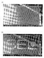
- FIGS. (A) And (B) The photograph explaining the display characteristic of the display panel which concerns on an Example.
- FIGS. 6A and 6B are diagrams illustrating characteristics of a display panel according to an embodiment.
- FIGS. 6A and 6B illustrate characteristics of a display panel according to an example.
- FIGS. 5A and 5B illustrate characteristics of liquid crystal elements according to examples.
- FIGS. 6A and 6B illustrate characteristics of a liquid crystal element according to an example.
- FIG. 6 is a diagram illustrating display performance of a display panel according to an example.
- FIG. 6 is a diagram illustrating display performance of a display panel according to an example.
- One embodiment of the present invention is a liquid crystal element including a first electrode, a second electrode, and a layer containing a liquid crystal material.
- the second electrode is disposed between the first electrode and the first electrode so as to form an electric field across the layer containing the liquid crystal material.
- the layer including the liquid crystal material scatters incident light with a first scattering intensity when the electric field is in the first state, and allows incident light with a second scattering intensity when the electric field is in a second state larger than the first state. Scattered.
- the second scattering intensity is greater than the first scattering intensity.
- the layer containing a liquid crystal material contains a liquid crystal material and a polymer material, and the layer containing a liquid crystal material is stabilized with a polymer.
- the polymer material is a copolymer of a polyfunctional monomer and a monofunctional monomer, the polyfunctional monomer has a phenyl benzoate skeleton, and the monofunctional monomer has a cyclohexylbenzene skeleton.
- FIG. 1A is a cross-sectional view illustrating the structure of the liquid crystal element of one embodiment of the present invention
- FIG. 1B is a top view illustrating the structure of the liquid crystal element of one embodiment of the present invention.
- a variable having an integer value of 1 or more may be used for the sign.
- (p) including a variable p that takes an integer value of 1 or more may be used as a part of a code that identifies any of the maximum p components.
- a variable m that takes an integer value of 1 or more and (m, n) including a variable n may be used as part of a code that identifies any of the maximum m ⁇ n components.
- a liquid crystal element 75 described in this embodiment includes an electrode 51, an electrode 52, and a layer 53 containing a liquid crystal material. In addition, it includes an alignment film AF1 and an alignment film AF2.
- the alignment film AF1 includes a region sandwiched between the electrode 51 and the layer 53 containing a liquid crystal material.
- the alignment film AF2 includes a region sandwiched between the electrode 52 and the layer 53 containing a liquid crystal material.
- An alignment film that aligns liquid crystals approximately in the horizontal direction can be used for the alignment film AF1 and the alignment film AF2.
- an angle of about 3 ° to 5 ° can be set as the pretilt angle.
- the alignment film AF2 is rubbed so as to be anti-parallel to the alignment film AF1. Further, the thickness of the alignment film AF1 or the alignment film AF2 can be set to, for example, 70 nm.
- the electrode 52 is disposed so as to form an electric field across the layer 53 containing a liquid crystal material between the electrode 52 and the electrode 51.
- the layer 53 containing a liquid crystal material scatters the incident light I 0 with the second scattering intensity in the second state where the electric field is larger than the first state. Note that the second scattering intensity is greater than the first scattering intensity.
- the thickness of the layer 53 containing a liquid crystal material can be set to 4 ⁇ m, for example.
- the layer 53 containing a liquid crystal material contains a liquid crystal material and a polymer material, and the layer 53 containing a liquid crystal material is stabilized with a polymer.
- liquid crystal material For example, a liquid crystal material MDA-00-3506 manufactured by Merck can be used for the layer 53 containing a liquid crystal material.
- the polymer material is a copolymer of a polyfunctional monomer and a monofunctional monomer.
- the polyfunctional monomer has a phenyl benzoate backbone.
- a diacrylate having a phenyl benzoate skeleton can be used as the polyfunctional monomer.
- a material represented by the following structural formula (1) can be used for the polyfunctional monomer.
- the monofunctional monomer has a cyclohexylbenzene skeleton.
- an acrylate having a cyclohexyl skeleton can be used as the monofunctional monomer.
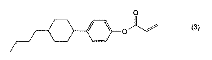
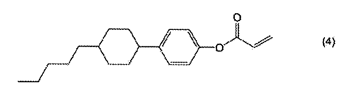
- materials represented by the following structural formulas (2) to (4) can be used for the monofunctional monomer.
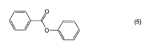
- phenyl benzoate has a structure represented by Structural Formula (5)
- cyclohexylbenzene has a structure represented by Structural Formula (6). Any of them may have a substituent.
- the second scattering intensity is 10 times or more the first scattering intensity.
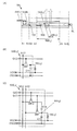
- FIG. 2 illustrates a structure of a display panel of one embodiment of the present invention.
- 2A is a top view of a display panel of one embodiment of the present invention, and
- FIG. 2B is a part of FIG.
- FIG. 3 illustrates a structure of a display panel of one embodiment of the present invention.
- 3A is a cross-sectional view taken along cutting lines X1-X2, X3-X4, and X9-X10 in FIG. 2A.
- FIGS. 3B and 3C illustrate pixel circuits 530 (i, j FIG.
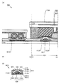
- FIG. 4 illustrates a structure of a display panel of one embodiment of the present invention.
- 4A is a cross-sectional view of the pixel 702 (i, j) in FIG. 2A
- FIG. 4B is a cross-sectional view illustrating part of FIG. 4A.
- the display panel 700 described in this embodiment includes a display region 231 and a functional layer 520 (see FIGS. 2A and 3A).
- the display area 231 includes a pixel 702 (i, j).
- the pixel 702 (i, j) includes a display element 750 (i, j) and a pixel circuit 530 (i, j).
- ⁇ Configuration Example of Pixel 702 (i, j) For example, the liquid crystal element 75 described in Embodiment 1 can be used for the display element 750 (i, j).
- the display element 750 (i, j) is electrically connected to the pixel circuit 530 (i, j).
- the functional layer 520 includes a pixel circuit 530 (i, j).
- the functional layer 520 includes an opening 591A.
- the pixel circuit 530 (i, j) is electrically connected to the display element 750 (i, j) (see FIG. 3A).
- a switch for example, a switch, a transistor, a diode, a resistor, an inductor, a capacitor, or the like can be used for the pixel circuit 530 (i, j).
- a transistor can be used for the switch.
- the pixel circuit 530 (i, j) includes a capacitive element C11 and a switch SW1.
- the capacitor C11 includes a first electrode that is electrically connected to the switch SW1 and a second electrode that is electrically connected to the wiring CSCOM.
- a bottom-gate transistor, a top-gate transistor, or the like can be used for the pixel circuit 530 (i, j).
- the transistor includes a semiconductor film 508, a conductive film 504, a conductive film 512A, and a conductive film 512B (see FIG. 4B).
- the semiconductor film 508 includes a region 508A electrically connected to the conductive film 512B and a region 508B electrically connected to the conductive film 512A.
- the semiconductor film 508 includes a region 508C between the region 508A and the region 508B.
- the conductive film 504 includes a region overlapping with the region 508C, and the conductive film 504 functions as a gate electrode.
- the insulating film 506 includes a region sandwiched between the semiconductor film 508 and the conductive film 504.
- the insulating film 506 has a function of a gate insulating film.
- the conductive film 512A has one of the function of the source electrode and the function of the drain electrode, and the conductive film 512B has the other of the function of the source electrode and the function of the drain electrode.
- the conductive film 524 can be used for a transistor.
- the conductive film 524 includes a region in which the semiconductor film 508 is sandwiched between the conductive film 504 and the conductive film 504.
- the conductive film 524 has a function of a gate electrode.
- the conductive film 524 can be electrically connected to the conductive film 504.
- the semiconductor film used for the transistor of the driver circuit can be formed.
- a semiconductor containing a Group 14 element can be used for the semiconductor film 508.
- a semiconductor containing silicon can be used for the semiconductor film 508.
- Hydroated amorphous silicon can be used for the semiconductor film 508.
- microcrystalline silicon or the like can be used for the semiconductor film 508. Accordingly, for example, a display panel with less display unevenness than a display panel using polysilicon as the semiconductor film 508 can be provided. Alternatively, the display panel can be easily increased in size.
- polysilicon can be used for the semiconductor film 508. Accordingly, for example, the field-effect mobility of the transistor can be higher than that of a transistor using hydrogenated amorphous silicon for the semiconductor film 508. Alternatively, for example, the driving ability can be increased as compared with a transistor using hydrogenated amorphous silicon for the semiconductor film 508. Alternatively, for example, the aperture ratio of the pixel can be improved over a transistor using hydrogenated amorphous silicon for the semiconductor film 508.
- the reliability of the transistor can be higher than that of a transistor using hydrogenated amorphous silicon for the semiconductor film 508.
- the temperature required for manufacturing the transistor can be lower than that of a transistor using single crystal silicon for the semiconductor film 508, for example.
- the semiconductor film used for the transistor of the driver circuit can be formed in the same process as the semiconductor film used for the transistor of the pixel circuit.
- the driver circuit can be formed over the same substrate as the pixel circuit. Alternatively, the number of parts included in the electronic device can be reduced.
- single crystal silicon can be used for the semiconductor film 508. Accordingly, for example, the definition can be increased as compared with a display panel using hydrogenated amorphous silicon for the semiconductor film 508. Alternatively, for example, a display panel with less display unevenness can be provided than a display panel using polysilicon as the semiconductor film 508. Or, for example, smart glasses or head mounted displays can be provided.
- a metal oxide can be used for the semiconductor film 508. Accordingly, as compared with a pixel circuit using a transistor using amorphous silicon as a semiconductor film, the time during which the pixel circuit can hold an image signal can be lengthened. Specifically, the selection signal can be supplied at a frequency of less than 30 Hz, preferably less than 1 Hz, more preferably less than once per minute while suppressing the occurrence of flicker. As a result, fatigue accumulated in the user of the information processing apparatus can be reduced. In addition, power consumption associated with driving can be reduced.
- a transistor including an oxide semiconductor can be used.
- an oxide semiconductor containing indium or an oxide semiconductor containing indium, gallium, and zinc can be used for the semiconductor film.
- a transistor whose leakage current in an off state is smaller than that of a transistor using amorphous silicon as a semiconductor film can be used.
- a transistor in which an oxide semiconductor is used for a semiconductor film can be used.
- a 25-nm-thick film containing indium, gallium, and zinc can be used for the semiconductor film 508.
- a conductive film in which a 10-nm-thick film containing tantalum and nitrogen and a 300-nm-thick film containing copper are stacked can be used for the conductive film 504.
- the film containing copper includes a region between which the film containing tantalum and nitrogen is sandwiched between the film containing copper.
- a stacked film in which a 400-nm-thick film containing silicon and nitrogen and a 200-nm-thick film containing silicon, oxygen, and nitrogen are stacked can be used for the insulating film 506.
- the film containing silicon and nitrogen includes a region between the semiconductor film 508 and the film containing silicon, oxygen, and nitrogen.
- the film containing tungsten includes a region in contact with the semiconductor film 508.
- a bottom-gate transistor production line using amorphous silicon as a semiconductor can be easily modified to a bottom-gate transistor production line using an oxide semiconductor as a semiconductor.
- a top gate transistor production line using polysilicon as a semiconductor can be easily modified to a top gate transistor production line using an oxide semiconductor as a semiconductor. Both modifications can make effective use of existing production lines.
- a compound semiconductor can be used for a semiconductor film of a transistor.
- a semiconductor containing gallium arsenide can be used for the semiconductor film.
- an organic semiconductor can be used for a semiconductor film of a transistor.
- an organic semiconductor containing polyacenes or graphene can be used for the semiconductor film.
- a pixel circuit 530 (i, j) in FIG. 3C is different from the structure described with reference to FIG. 3B in that a capacitor C12 and a switch SW12 are provided.
- a capacitor C12 and a switch SW12 are provided.
- Capacitance element C12 includes a first terminal electrically connected to node N1 (i, j). The capacitive element C12 includes a second terminal that is electrically connected to the switch SW12.
- the switch SW12 includes a first terminal to which a control signal is supplied.
- the switch SW12 includes a second terminal that is electrically connected to the node N1 (i, j).
- a transistor can be used for the switch SW12.
- One of a source electrode and a drain electrode of the transistor can be used for the first terminal and the other can be used for the second terminal.
- the switch SW12 is in a conductive state when the switch SW1 changes from a conductive state to a non-conductive state.
- the switch SW12 has a function of changing from a non-conductive state to a conductive state when the switch SW1 is in a non-conductive state.
- the switch SW12 has a function of changing from a conductive state to a non-conductive state when the switch SW1 is in a non-conductive state.
- the conduction state of the switch SW1 or the switch SW12 using a transistor can be controlled using the potential of the gate electrode of the transistor.
- the potential of the node N1 (i, j) can be controlled using the switch SW1.
- the switch SW12 can be used to temporarily promote or emphasize the change in potential of the node N1 (i, j).
- overdrive can be performed.
- the operation of the liquid crystal display element can be speeded up. As a result, a novel display panel that is highly convenient or reliable can be provided.
- the functional layer 520 includes an insulating film 521A, an insulating film 518, an insulating film 516A, an insulating film B, an insulating film 506, an insulating film 501C, and the like (see FIGS. 4A and 4B).
- the insulating film 521A includes a region sandwiched between the pixel circuit 530 (i, j) and the display element 750 (i, j).
- the insulating film 518 includes a region sandwiched between the insulating film 521A and the insulating film 501C.
- the insulating film 516 includes a region sandwiched between the insulating film 518 and the insulating film 501C.
- the insulating film 506 includes a region sandwiched between the insulating film 516 and the insulating film 501C.
- Insulating film 521A For example, an insulating inorganic material, an insulating organic material, or an insulating composite material including an inorganic material and an organic material can be used for the insulating film 521A.
- an inorganic oxide film, an inorganic nitride film, an inorganic oxynitride film, or the like, or a stacked material in which a plurality selected from these films is stacked can be used for the insulating film 521A.
- a film including a silicon oxide film, a silicon nitride film, a silicon oxynitride film, an aluminum oxide film, or the like, or a stacked material in which a plurality selected from these films is stacked can be used for the insulating film 521A.
- the silicon nitride film is a dense film and has an excellent function of suppressing impurity diffusion.
- the insulating film 521A can planarize steps resulting from various structures overlapping with the insulating film 521A, for example.
- polyimide has characteristics superior to other organic materials in characteristics such as thermal stability, insulation, toughness, low dielectric constant, low thermal expansion coefficient, and chemical resistance.
- polyimide can be suitably used for the insulating film 521A and the like.
- a film formed using a photosensitive material can be used for the insulating film 521A.
- a film formed using photosensitive polyimide, photosensitive acrylic resin, or the like can be used for the insulating film 521A.
- Insulating film 518 For example, a material that can be used for the insulating film 521A can be used for the insulating film 518.
- a material having a function of suppressing diffusion of oxygen, hydrogen, water, alkali metal, alkaline earth metal, or the like can be used for the insulating film 518.
- a nitride insulating film can be used for the insulating film 518.
- silicon nitride, silicon nitride oxide, aluminum nitride, aluminum nitride oxide, or the like can be used for the insulating film 518. Thereby, diffusion of impurities into the semiconductor film of the transistor can be suppressed.
- Insulating film 516 For example, a material that can be used for the insulating film 521A can be used for the insulating film 516.
- a film whose manufacturing method is different from that of the insulating film 518 can be used for the insulating film 516.
- Insulating film 506 For example, a material that can be used for the insulating film 521A can be used for the insulating film 506.
- a film including a lanthanum oxide film, a cerium oxide film, or a neodymium oxide film can be used for the insulating film 506.
- the insulating film 501D includes a region sandwiched between the insulating film 501C and the insulating film 516.
- a material that can be used for the insulating film 506 can be used for the insulating film 501D.
- Insulating film 501C For example, a material that can be used for the insulating film 521A can be used for the insulating film 501C. Specifically, a material containing silicon and oxygen can be used for the insulating film 501C. Thereby, diffusion of impurities into the pixel circuit or the display element can be suppressed.
- the display panel 700 includes a base material 510, a base material 770, and a sealing material 705 (see FIGS. 4A and 5A).
- Base Material 510 Base Material 770
- a material having a light-transmitting property can be used for the substrate 510 or the substrate 770.
- a flexible material can be used for the base 510 or the base 770.
- a flexible display panel can be provided.
- a material having a thickness of 0.7 mm or less and a thickness of 0.1 mm or more can be used for the substrate 510 or the substrate 770. Specifically, a material polished to a thickness of about 0.1 mm can be used. Thereby, the weight of the base material 510 or the base material 770 can be reduced.
- glass substrates of 6th generation (1500 mm ⁇ 1850 mm), 7th generation (1870 mm ⁇ 2200 mm), 8th generation (2200 mm ⁇ 2400 mm), 9th generation (2400 mm ⁇ 2800 mm), 10th generation (2950 mm ⁇ 3400 mm), etc. can be used for the substrate 510 or the substrate 770.
- a large display device can be manufactured.
- An organic material, an inorganic material, a composite material of an organic material and an inorganic material, or the like can be used for the base material 510 or the base material 770.
- inorganic materials such as glass, ceramics, and metal can be used.
- alkali-free glass, soda-lime glass, potash glass, crystal glass, aluminosilicate glass, tempered glass, chemically tempered glass, quartz, sapphire, or the like can be used for the base material 510 or the base material 770.
- aluminosilicate glass, tempered glass, chemically tempered glass, sapphire, or the like can be suitably used for the base material 510 or the base material 770 that is disposed on the side close to the user of the display panel. Thereby, it is possible to prevent the display panel from being damaged or damaged due to use.
- an inorganic oxide film, an inorganic nitride film, an inorganic oxynitride film, or the like can be used for the base material 510 or the base material 770.
- a silicon oxide film, a silicon nitride film, a silicon oxynitride film, an aluminum oxide film, or the like can be used.
- Stainless steel, aluminum, or the like can be used for the substrate 510 or the substrate 770.
- a single crystal semiconductor substrate made of silicon or silicon carbide, a polycrystalline semiconductor substrate, a compound semiconductor substrate such as silicon germanium, an SOI substrate, or the like can be used for the base 510 or the base 770.
- the semiconductor element can be formed on the base 510 or the base 770.
- an organic material such as a resin, a resin film, or plastic can be used for the base 510 or the base 770.
- a material containing polyester, polyolefin, polyamide (such as nylon or aramid), polyimide, polycarbonate, polyurethane, an acrylic resin, an epoxy resin, or a resin having a siloxane bond is used for the base 510 or the base 770.
- a resin film, a resin plate, or a laminated material containing these materials can be used. Thereby, a weight can be reduced. Or, for example, it is possible to reduce the frequency of occurrence of breakage due to dropping.
- PET polyethylene terephthalate
- PEN polyethylene naphthalate
- PES polyethersulfone
- COP cycloolefin polymer
- COC cycloolefin copolymer
- a composite material in which a metal plate, a thin glass plate, or a film of an inorganic material and a resin film are bonded to each other can be used for the base material 510 or the base material 770.
- a composite material in which a fibrous or particulate metal, glass, inorganic material, or the like is dispersed in a resin can be used for the base material 510 or the base material 770.
- a composite material in which a fibrous or particulate resin, an organic material, or the like is dispersed in an inorganic material can be used for the base material 510 or the base material 770.
- a single layer material or a material in which a plurality of layers are stacked can be used for the base material 510 or the base material 770.
- a material in which an insulating film or the like is stacked can be used for the base material 510 or the base material 770.
- a material in which one or a plurality of films selected from a silicon oxide layer, a silicon nitride layer, a silicon oxynitride layer, or the like is stacked can be used for the base material 510 or the base material 770.
- diffusion of impurities contained in the base material can be prevented.
- diffusion of impurities contained in glass or resin can be prevented.
- diffusion of impurities that permeate the resin can be prevented.
- paper, wood, or the like can be used for the base material 510 or the base material 770.
- a material having heat resistance high enough to withstand heat treatment in the manufacturing process can be used for the base material 510 or the base material 770.
- a material having heat resistance to heat applied during a manufacturing process for directly forming a transistor, a capacitor, or the like can be used for the base material 510 or the base material 770.
- an insulating film, a transistor, a capacitor, or the like is formed over a process substrate that has heat resistance to heat applied during the manufacturing process, and the formed insulating film, transistor, or capacitor, for example, a base 510 or a base A method of transposing to 770 can be used. Accordingly, for example, an insulating film, a transistor, a capacitor, or the like can be formed over a flexible substrate.
- the sealing material 705 includes a region sandwiched between the base material 510 and the base material 770 and has a function of bonding the base material 510 and the base material 770 together (see FIG. 5A).
- An inorganic material, an organic material, a composite material of an inorganic material and an organic material, or the like can be used for the sealant 705.
- an organic material such as a heat-meltable resin or a curable resin can be used for the sealing material 705.
- an organic material such as a reactive curable adhesive, a photocurable adhesive, a thermosetting adhesive, and / or an anaerobic adhesive can be used for the sealant 705.
- an adhesive including epoxy resin, acrylic resin, silicone resin, phenol resin, polyimide resin, imide resin, PVC (polyvinyl chloride) resin, PVB (polyvinyl butyral) resin, EVA (ethylene vinyl acetate) resin, etc. Can be used for the sealant 705.
- the display panel 700 includes a functional film 770P (see FIG. 4A).
- the functional film 770P includes a region overlapping with the display element 750 (i, j).
- an antireflection film for example, an antireflection film, a polarizing film, a retardation film, a light diffusion film, a light collecting film, or the like can be used for the functional film 770P.
- an antireflection film having a thickness of 1 ⁇ m or less can be used for the functional film 770P.
- a multilayer film in which three or more dielectric layers, preferably five or more layers, more preferably 15 or more layers are stacked can be used for the functional film 770P. Thereby, a reflectance can be suppressed to 0.5% or less, preferably 0.08% or less.
- antistatic film that suppresses adhesion of dust
- water-repellent film that makes it difficult to adhere dirt
- antireflection film anti-reflection film
- non-glossy film anti-glare film
- scratches caused by use A hard coat film or the like that suppresses the above can be used for the functional film 770P.
- the display panel 700 includes a structure KB1.
- the structure KB1 has a function of providing a predetermined gap between the functional layer 520 and the base material 770.
- the display element 750 (i, j) has a function of controlling light scattering or transmission, for example.
- the liquid crystal element 75 described in Embodiment 1 can be used for the display element 750 (i, j).
- the display element 750 (i, j) includes a layer 753 containing a liquid crystal material (see FIG. 4A).
- scattering or transmission of light can be controlled to display an image.
- scenery or the like can be observed through the display element 750 (i, j).
- an image can be displayed over the landscape.
- an image can be displayed by scattering light emitted from the sidelight.
- the display element 750 (i, j) includes an electrode 751 (i, j), an electrode 752, and a layer 753 containing a liquid crystal material.
- the electrode 751 (i, j) is electrically connected to the pixel circuit 530 (i, j) at the opening 591A.
- the electrode 752 is disposed so as to form an electric field for controlling the alignment of the liquid crystal material between the electrode 751 (i, j).
- the display element 750 (i, j) includes an alignment film AF1 and an alignment film AF2.
- the layer 753 containing a liquid crystal material includes a region sandwiched between the alignment film AF1 and the alignment film AF2.
- a liquid crystal material having a specific resistivity of 1.0 ⁇ 10 13 ⁇ ⁇ cm or more, preferably 1.0 ⁇ 10 14 ⁇ ⁇ cm or more, and more preferably 1.0 ⁇ 10 15 ⁇ ⁇ cm or more is used.
- the layer 753 containing a material can be used. Thereby, the fluctuation
- FIG. 6 is a block diagram illustrating a structure of a display panel of one embodiment of the present invention.
- a display panel 700 described in this embodiment includes a display region 231 (see FIG. 6).
- the display region 231 includes a group of pixels 702 (i, 1) to 702 (i, n), another group of pixels 702 (1, j) to 702 (m, j), and a scanning line G1 (i ) And a signal line S1 (i) (see FIG. 6).
- i is an integer of 1 to m
- j is an integer of 1 to n
- m and n are integers of 1 or more.
- the display region 231 includes a conductive film VCOM1.
- the group of pixels 702 (i, 1) to 702 (i, n) are arranged in the row direction (the direction indicated by the arrow R1 in the figure), and the group of pixels 702 (i, 1) to 702 (i, n n) includes pixel 702 (i, j).
- Another group of pixels 702 (1, j) to 702 (m, j) is arranged in a column direction (direction indicated by an arrow C1 in the drawing) intersecting the row direction, and another group of pixels 702 (1 , J) through pixel 702 (m, j) include pixel 702 (i, j).
- the scan line G1 (i) is electrically connected to a group of the pixels 702 (i, 1) to 702 (i, n) arranged in the row direction.
- the signal line S1 (j) is electrically connected to another group of the pixels 702 (1, j) to 702 (m, j) arranged in the column direction.
- image information can be supplied to a plurality of pixels.
- a novel display panel that is highly convenient or reliable can be provided.
- a display panel 700 described in this embodiment includes one or a plurality of driving circuits.
- a drive circuit GDA, a drive circuit GDB, and a drive circuit SD can be provided (see FIG. 6).
- Drive circuit GDA, drive circuit GDB can be used for the drive circuit GD.
- the drive circuit GDA and the drive circuit GDB have a function of supplying a selection signal based on the control information.
- a function of supplying a selection signal to one scanning line at a frequency of 30 Hz or more, preferably 60 Hz or more based on the control information is provided. Thereby, a moving image can be displayed smoothly.
- a function of supplying a selection signal to one scan line at a frequency of less than 30 Hz, preferably less than 1 Hz, more preferably less than once per minute based on the control information is provided. Thereby, a still image in which flicker is suppressed can be displayed.
- the frequency with which the drive circuit GDA supplies the selection signal and the frequency with which the drive circuit GDB supplies the selection signal can be made different.
- the selection signal can be supplied to another region displaying the moving image at a frequency higher than the frequency of supplying the selection signal to one region displaying the still image.
- the frame frequency can be made variable.
- display can be performed at a frame frequency of 1 Hz to 120 Hz.
- display can be performed at a frame frequency of 120 Hz using a progressive method.
- a bottom-gate transistor, a top-gate transistor, or the like can be used for the driver circuit GD.
- the transistor MG1 can be used for the drive circuit GD (see FIG. 5).
- a semiconductor film used for a transistor of the driver circuit GD can be formed in a step of forming a semiconductor film used for a transistor of the pixel circuit 530 (i, j).
- the drive circuit SD has a function of generating an image signal based on the information V11 and a function of supplying the image signal to a pixel circuit that is electrically connected to one display element (see FIG. 6).
- various sequential circuits such as a shift register can be used for the drive circuit SD.
- an integrated circuit formed on a silicon substrate can be used for the drive circuit SD.
- the integrated circuit can be connected to a terminal by using a COG (Chip on glass) method or a COF (Chip on Film) method.
- a COG Chip on glass
- COF Chip on Film
- an integrated circuit can be connected to a terminal using an anisotropic conductive film.
- FIG. 7 illustrates a structure of a display device of one embodiment of the present invention.
- FIG. 7A is a block diagram of a display device of one embodiment of the present invention
- FIGS. 7B-1 to 7B-3 are projections illustrating the appearance of the display device of one embodiment of the present invention.
- FIG. 7A is a block diagram of a display device of one embodiment of the present invention
- FIGS. 7B-1 to 7B-3 are projections illustrating the appearance of the display device of one embodiment of the present invention.
- FIG. 7A is a block diagram of a display device of one embodiment of the present invention
- FIGS. 7B-1 to 7B-3 are projections illustrating the appearance of the display device of one embodiment of the present invention.
- the display device described in this embodiment includes a control portion 238 and a display panel 700 (see FIG. 7A).
- the control unit 238 is supplied with the image information V1 and the control information CI.
- a clock signal or a timing signal can be used for the control information CI.
- the control unit 238 generates information V11 based on the image information V1, and generates a control signal SP based on the control information CI. In addition, the control unit 238 supplies information V11 and a control signal SP.
- the information V11 includes a gradation of 8 bits or more, preferably 12 bits or more.
- a clock signal or a start pulse of a shift register used for the driver circuit can be used for the control signal SP.
- control unit 238 includes a control circuit 233, an expansion circuit 234, and an image processing circuit 235.
- the expansion circuit 234 has a function of expanding the image information V1 supplied in a compressed state.
- the decompression circuit 234 includes a storage unit.
- the storage unit has a function of storing, for example, decompressed image information.
- the image processing circuit 235 includes a storage area, for example.
- the storage area has a function of storing information included in the image information V1, for example.
- the image processing circuit 235 includes, for example, a function of correcting the image information V1 based on a predetermined characteristic curve to generate information V11 and a function of supplying information V11.
- the display panel 700 is supplied with information V11 and a control signal SP.
- the display panel 700 includes a drive circuit GD.
- the display panel 700 described in Embodiment 2 can be used.
- control circuit 233 can be used for the display panel 700.
- driver circuit GD can be used for the display panel 700.
- Control circuit 233 has a function of generating and supplying the control signal SP.
- a clock signal or a timing signal can be used as the control signal SP.
- a timing controller can be used for the control circuit 233.
- control circuit 233 formed over a rigid substrate can be used for the display panel 700.
- control circuit 233 and the control unit 238 formed on the rigid board can be electrically connected using a flexible printed board.
- the drive circuit GD operates based on the control signal SP.
- the drive circuit GDA (1), the drive circuit GDA (2), the drive circuit GDB (1), and the drive circuit GDB (2) have a function of supplying a selection signal and a control signal SP.
- the drive circuit SDA (1), the drive circuit SDA (2), the drive circuit SDB (1), the drive circuit SDB (2), the drive circuit SDC (1), and the drive circuit SDC (2) V11 is supplied, and an image signal can be supplied.
- control signal SP By using the control signal SP, the operations of the plurality of drive circuits can be synchronized.
- a novel display device that is highly convenient or reliable can be provided.
- a television receiving system see FIG. 7B-1
- a video monitor see FIG. 7B-2
- a notebook computer see FIG. 7B-3
- Non-alkali glass was used as the substrate.
- a transparent conductive film was formed on the substrate and used as an electrode.
- An alignment film AF1 was formed on the electrode 51, and an alignment film AF2 was formed on the electrode 52.
- the alignment film AF1 was rubbed so as to be aligned in the horizontal direction, and the alignment film AF2 was rubbed so as to be anti-parallel to the alignment film AF1.
- a composition containing a liquid crystal material, a polyfunctional monomer, and a monofunctional monomer was sealed between the electrode 51 and the electrode 52 using a sealing material, and the layer 53 containing the liquid crystal material was polymerized. Specifically, the composition was irradiated with ultraviolet rays at 30 ° C. to form a layer 53 containing a liquid crystal material. Note that the cell gap was provided so that the layer 53 containing the liquid crystal material had a thickness of 4.0 ⁇ m.
- a device E was produced using a bifunctional monomer represented by the following structural formula (8).
- the material represented by the structural formula (7) and the polyfunctional monomer represented by the structural formula (8) both have a phenyl benzoate skeleton.
- the element of the comparative example 1 was produced using the bifunctional monomer represented by Structural formula (1)
- the element of the comparative example 2 was produced using the bifunctional monomer represented by Structural formula (7).
- symbol LC-1 corresponds to a liquid crystal material (Merck MDA-00-3506).
- the symbol DM-1 corresponds to the bifunctional monomer represented by the structural formula (1)
- the symbol DM-2 corresponds to the bifunctional monomer represented by the structural formula (7)
- the symbol DM-3 represents the structural formula ( This corresponds to the bifunctional monomer represented by 8).
- the symbol MM-1 corresponds to the monofunctional monomer represented by the structural formula (2)
- the symbol MM-2 corresponds to the monofunctional monomer represented by the structural formula (3)
- the symbol MM-3 represents the structural formula ( This corresponds to the monofunctional monomer represented by 4).
- the liquid crystal material was mixed and used so that it might become 92.5 weight% and the monomer might be 7.5 weight%.
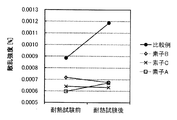
- element A, element B, and element C had a lower scattering intensity than the liquid crystal element of Comparative Example 1.
- the added monofunctional monomer suppressed light scattering and improved the transparency of the liquid crystal element 75.
- the element A, the element B, and the element C had lower scattering intensity than the liquid crystal element of Comparative Example 1. Moreover, the change accompanying the heat resistance test of scattering intensity was suppressed. In other words, the added monofunctional monomer improved the reliability of the liquid crystal element 75.
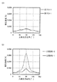
- Comparative Example 2 For Comparative Example 2, the dependence of the scattering intensity on the incident light azimuth was measured (see FIG. 10B). The result about Comparative Example 2 before the heat resistance test is shown as Comparative Example 2-1, and the result about Comparative Example 2 after the heat resistance test is shown as Comparative Example 2-2.
- the scattering intensity of the element D is small. Compared with Comparative Example 2, the change accompanying the heat resistance test of the scattering intensity of the element D was also suppressed. In other words, the added monofunctional monomer improved the reliability of the liquid crystal element.
- the dependence of the scattering intensity on the incident light azimuth was also measured (see FIG. 11A).
- the result about the element E before the heat resistance test is shown as an element E-1, and the result about the element E after the heat resistance test is shown as an element E-2.
- the change accompanying the heat resistance test of the scattering intensity of the element E is small.
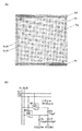
- FIG. 13 illustrates a structure of a display panel of one embodiment of the present invention.
- FIG. 13A is a top view of a pixel of a display panel of one embodiment of the present invention
- FIG. 13B is a circuit diagram of a pixel circuit and a display element.
- FIG. 14 illustrates the wavelength dependency of the transmittance of the display panel of one embodiment of the present invention.
- FIG. 15 illustrates display performance of the display panel of one embodiment of the present invention.
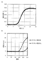
- FIG. 16 illustrates characteristics of the liquid crystal element of one embodiment of the present invention.
- 16A is a characteristic curve illustrating the dependence of the scattering intensity of the liquid crystal element of one embodiment of the present invention on applied voltage
- FIG. 16B illustrates the display characteristics of the liquid crystal element of one embodiment of the present invention.
- FIG. 17 illustrates the dependence of the dielectric constant of a layer including a liquid crystal material used on the liquid crystal element of one embodiment of the present invention on applied voltage.
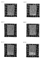
- FIG. 18 illustrates display performance of the display panel of one embodiment of the present invention.
- 18 (A-1), 18 (B-1), and 18 (C-1) are photographs for explaining the result of display using only the image signal
- FIG. 18 (A-2), FIG. 18B-2 and FIG. 18C-2 are photographs illustrating the results of display using image signals and control signals.
- the display device has a display panel and a light source.
- the drive circuit GD was operated using a signal having a frequency of 37.31 kHz as a clock signal. Further, the drive circuit GD was able to supply a signal having a voltage of ⁇ 35V and a signal having a voltage of + 20V.
- the voltage applied to the display element 750 (i, j) was inverted by controlling the potential of the conductive film VCOM1 to be ⁇ 15V and + 15V.
- the drive circuit SD was operated with one horizontal period set to 6.7 ⁇ sec. Further, the drive circuit SD was able to supply a signal having a voltage of ⁇ 9V and a signal having a + 9V.
- the transmittance of the manufactured display panel was about 62% near a wavelength of 550 nm.
- the image Image1 was displayed on the produced display device (see FIG. 15).
- the image Image2 that can be seen in the display area 231 is the appearance of a printed material that is placed on the other side of the display panel.
- the image Image2 is an appearance of a printed matter that can be seen through the transparent portion of the display area 231.
- FIG. 18A-2 is a display in which a control signal is added to the image signal displayed in FIG. 18A-1
- FIG. 18B-2 is displayed in FIG. 18B-1
- FIG. 18C-2 is a display in which a control signal is added to the image signal displayed in FIG. 18C-1.
- the contrast ratio could be increased by using the image signal and the control signal.
- a signal of 256 gradations was displayed on the manufactured liquid crystal element (see FIG. 16B).
- the scattering intensity can be increased as compared with the case where only the 256 gradation signal is displayed on the liquid crystal element.
- the light incident from the side surface of the display panel using the edge light was scattered in the front direction of the display panel, etc., and the front luminance could be increased.
- Non-alkali glass was used as the substrate.
- a transparent conductive film formed on the substrate was used as an electrode.
- the alignment film AF1 was formed on the electrode 51 on one substrate, and the alignment film AF2 was formed on the electrode 52 on the other substrate.
- the alignment film AF1 was rubbed so as to be aligned in the horizontal direction, and the alignment film AF2 was rubbed so as to be aligned in antiparallel with the alignment film AF1.
- a composition containing a liquid crystal material, a polyfunctional monomer, and a monofunctional monomer was sealed between the electrode 51 and the electrode 52 using a sealing material, and the layer 53 containing the liquid crystal material was stabilized with a polymer.
- the composition 53 was irradiated with ultraviolet rays to form a layer 53 containing a liquid crystal material. Note that a cell gap was provided so that the layer 53 containing a liquid crystal material had a thickness of 4.0 ⁇ m, and the layer 53 was formed at three different temperatures of 30 ° C., 40 ° C., and 50 ° C.
- the symbol DM-4 corresponds to the bifunctional monomer represented by the structural formula (9).
- the polymerization initiator represented by Structural Formula (10) was used for polymer stabilization.
- the addition amount of the polymerization initiator was 0.1% by weight of the composition.
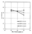
- Contrast ratios were measured for the elements F1 to F3, the elements G1 to G3, and the elements H1 to H3 (see FIG. 19). Both elements had a large contrast ratio of 25 or more.
- the elements H1 to H3 not only have a high contrast ratio, but also have a small temperature dependency when the polymer is stabilized.
- the structure and evaluation results of the manufactured liquid crystal element of one embodiment of the present invention will be described with reference to FIGS.
- the liquid crystal element produced in this example differs from that in Example 3 in the configuration of the layer 53 containing a liquid crystal material.
- a bifunctional monomer different from that in Example 3 was used when forming a layer containing a liquid crystal material.
- different portions will be described in detail, and the above description will be applied to portions that can use the same configuration.
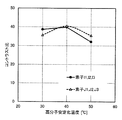
- Contrast ratios were measured for the elements I1 to I3 and the elements J1 to J3 (see FIG. 20). Both elements had a large contrast ratio of 30 or more. In particular, the element J2 has a high contrast ratio of 40 or more.
- X and Y are assumed to be objects (for example, devices, elements, circuits, wirings, electrodes, terminals, conductive films, layers, etc.).
- an element for example, a switch, a transistor, a capacitive element, an inductor, a resistance element, a diode, a display, etc.
- Element, light emitting element, load, etc. are not connected between X and Y, and elements (for example, switches, transistors, capacitive elements, inductors) that allow electrical connection between X and Y X and Y are connected without passing through a resistor element, a diode, a display element, a light emitting element, a load, or the like.
- an element for example, a switch, a transistor, a capacitive element, an inductor, a resistance element, a diode, a display, etc.
- the switch has a function of controlling on / off. That is, the switch is in a conductive state (on state) or a non-conductive state (off state), and has a function of controlling whether or not to pass a current. Alternatively, the switch has a function of selecting and switching a path through which a current flows.
- the case where X and Y are electrically connected includes the case where X and Y are directly connected.
- a circuit for example, a logic circuit (an inverter, a NAND circuit, a NOR circuit, etc.) that enables a functional connection between X and Y, signal conversion, etc.
- Circuit (DA conversion circuit, AD conversion circuit, gamma correction circuit, etc.), potential level conversion circuit (power supply circuit (boost circuit, step-down circuit, etc.), level shifter circuit that changes signal potential level, etc.), voltage source, current source, switching Circuit, amplifier circuit (circuit that can increase signal amplitude or current amount, operational amplifier, differential amplifier circuit, source follower circuit, buffer circuit, etc.), signal generation circuit, memory circuit, control circuit, etc.)
- a circuit for example, a logic circuit (an inverter, a NAND circuit, a NOR circuit, etc.) that enables a functional connection between X and Y, signal conversion, etc.
- Circuit (DA conversion circuit, AD conversion circuit, gamma correction circuit, etc.), potential level conversion circuit (power supply circuit (boost circuit, step-down
- X and Y are functionally connected.
- the case where X and Y are functionally connected includes the case where X and Y are directly connected and the case where X and Y are electrically connected.
- the source (or the first terminal) of the transistor is electrically connected to X through (or not through) Z1, and the drain (or the second terminal or the like) of the transistor is connected to Z2.
- Y is electrically connected, or the source (or the first terminal, etc.) of the transistor is directly connected to a part of Z1, and another part of Z1 Is directly connected to X, and the drain (or second terminal, etc.) of the transistor is directly connected to a part of Z2, and another part of Z2 is directly connected to Y.
- X and Y, and the source (or the first terminal or the like) and the drain (or the second terminal or the like) of the transistor are electrically connected to each other.
- the drain of the transistor (or the second terminal, etc.) and the Y are electrically connected in this order.
- the source (or the first terminal or the like) of the transistor is electrically connected to X
- the drain (or the second terminal or the like) of the transistor is electrically connected to Y
- X or the source ( Or the first terminal or the like, the drain of the transistor (or the second terminal, or the like) and Y are electrically connected in this order.
- X is electrically connected to Y through the source (or the first terminal) and the drain (or the second terminal) of the transistor, and X is the source of the transistor (or the first terminal). Terminal, etc.), the drain of the transistor (or the second terminal, etc.), and Y are provided in this connection order.
- Terminal, etc.), the drain of the transistor (or the second terminal, etc.), and Y are provided in this connection order.
- a source (or a first terminal or the like of a transistor) is electrically connected to X through at least a first connection path, and the first connection path is The second connection path does not have a second connection path, and the second connection path includes a transistor source (or first terminal or the like) and a transistor drain (or second terminal or the like) through the transistor.
- the first connection path is a path through Z1
- the drain (or the second terminal, etc.) of the transistor is electrically connected to Y through at least the third connection path.
- the third connection path is connected and does not have the second connection path, and the third connection path is a path through Z2.
- the source (or the first terminal or the like) of the transistor is electrically connected to X via Z1 by at least a first connection path, and the first connection path is a second connection path.
- the second connection path has a connection path through the transistor, and the drain (or the second terminal, etc.) of the transistor is at least connected to Z2 by the third connection path.
- Y, and the third connection path does not have the second connection path.
- the source of the transistor (or the first terminal or the like) is electrically connected to X through Z1 by at least a first electrical path, and the first electrical path is a second electrical path Does not have an electrical path, and the second electrical path is an electrical path from the source (or first terminal or the like) of the transistor to the drain (or second terminal or the like) of the transistor;
- the drain (or the second terminal or the like) of the transistor is electrically connected to Y through Z2 by at least a third electrical path, and the third electrical path is a fourth electrical path.
- the fourth electrical path is an electrical path from the drain (or second terminal or the like) of the transistor to the source (or first terminal or the like) of the transistor.
- X, Y, Z1, and Z2 are objects (for example, devices, elements, circuits, wirings, electrodes, terminals, conductive films, layers, and the like).
- the term “electrically connected” in this specification includes in its category such a case where one conductive film has functions of a plurality of components.
- AF1 alignment film
- AF2 alignment film
- C11 capacitive element
- C12 capacitive element
- CI control information
- GD drive circuit
- GDA drive circuit
- GDB drive circuit
- KB1 Structure
- MG1 transistor
- S1 signal line
- SD drive circuit
- SDC (1) Drive circuit
- SDC (2) Drive circuit
- SP Control signal
- V1 Image information
- V11 Information
- VCOM1 Conductive film
- 50 Liquid crystal element
- 51 Electrode 52: electrode, 53: layer containing liquid crystal material
- 75 liquid crystal element
- 231 display region
- 233 control circuit
- 234 expansion circuit
- 235 image processing circuit
- 238 control unit
- 501C insulating film
- 50 D insulating film
- 504 conductive film
- 506 insulating film
Landscapes
- Physics & Mathematics (AREA)
- Chemical & Material Sciences (AREA)
- Nonlinear Science (AREA)
- Dispersion Chemistry (AREA)
- Mathematical Physics (AREA)
- Crystallography & Structural Chemistry (AREA)
- General Physics & Mathematics (AREA)
- Optics & Photonics (AREA)
- Liquid Crystal (AREA)
Abstract
利便性または信頼性に優れた新規な液晶素子を提供する。また、利便性または信頼性に優れた新規な表示パネルを提供する。 第1の電極(51)と第2の電極(52)と液晶材料を含む層(53)とを有する液晶素子(75)であって、第2の電極は第1の電極との間に、液晶材料を含む層を横切る電界を形成するように配置される。液晶材料を含む層は、電界が第1の状態において、入射光を第1の散乱強度で散乱し、電界が第1の状態より大きい第2の状態において、入射光を第2の散乱強度で散乱する。第2の散乱強度は、第1の散乱強度より大きい。液晶材料を含む層は液晶材料および尚分子材料を含み、液晶材料を含む層は尚分子で安定化される。高分子材料は多官能モノマーおよび単官能モノマーの共重合体であり、多官能モノマーは安息香酸フエニル骨格を備え、単官能モノマーはシクロへキシルべンゼン骨格を備える。
Description
本発明の一態様は、液晶素子、表示パネル、表示装置または半導体装置に関する。
なお、本発明の一態様は、上記の技術分野に限定されない。本明細書等で開示する発明の一態様の技術分野は、物、方法、または、製造方法に関するものである。または、本発明の一態様は、プロセス、マシン、マニュファクチャ、または、組成物(コンポジション・オブ・マター)に関するものである。そのため、より具体的に本明細書で開示する本発明の一態様の技術分野としては、半導体装置、表示装置、発光装置、蓄電装置、記憶装置、それらの駆動方法、または、それらの製造方法、を一例として挙げることができる。
光透過性を有する第1基板と、前記第1基板と対向し光透過性を有する第2基板と、前記第1基板と前記第2基板との間に配置された光変調層と、画像を表示する表示領域と法線方向で対向する位置の外側から前記光変調層を照明する光源ユニットと、前記第1基板に配置され、それぞれレッド、グリーン、またはブルーの互いに異なる色の第1乃至第3カラーフィルタと、前記第1乃至第3カラーフィルタにそれぞれ対向する第1乃至第3電極と、を備え、前記光変調層は、前記第1乃至第3電極のそれぞれによって生じる電場に応じて、前記第1乃至第3カラーフィルタのそれぞれに対向する領域の光散乱性を変調可能である、表示装置が知られている(特許文献1)。
本発明の一態様は、利便性または信頼性に優れた新規な液晶素子を提供することを課題の一とする。または、利便性または信頼性に優れた新規な表示パネルを提供することを課題の一とする。または、利便性または信頼性に優れた新規な表示装置を提供することを課題の一とする。または、新規な液晶素子、新規な表示パネル、新規な表示装置または新規な半導体装置を提供することを課題の一とする。
なお、これらの課題の記載は、他の課題の存在を妨げるものではない。なお、本発明の一態様は、これらの課題の全てを解決する必要はないものとする。なお、これら以外の課題は、明細書、図面、請求項などの記載から、自ずと明らかとなるものであり、明細書、図面、請求項などの記載から、これら以外の課題を抽出することが可能である。
(1)本発明の一態様は、第1の電極と、第2の電極と、液晶材料を含む層と、第1の配向膜と、第2の配向膜と、を有する液晶素子である。
第1の配向膜は、第1の電極および液晶材料を含む層の間に挟まれる領域を備え、第2の配向膜は、第2の電極および液晶材料を含む層の間に挟まれる領域を備える。
第2の電極は第1の電極との間に、液晶材料を含む層を横切る電界を形成するように配置される。
液晶材料を含む層は電界が第1の状態において、入射光を第1の散乱強度で散乱する。また、液晶材料を含む層は電界が第1の状態より大きい第2の状態において、入射光を第2の散乱強度で散乱する。なお、第2の散乱強度は、第1の散乱強度より大きい。
液晶材料を含む層は液晶材料および高分子材料を含み、液晶材料を含む層は高分子で安定化される。
高分子材料は多官能モノマーおよび単官能モノマーの共重合体であり、多官能モノマーは安息香酸フェニル骨格を備え、単官能モノマーはシクロヘキシルベンゼン骨格を備える。
これにより、電界が第1の状態より大きい第2の状態において、入射光をより強く散乱することができる。または、入射光を透過しやすい状態において消費する電力を少なくできる。その結果、利便性または信頼性に優れた新規な液晶素子を提供することができる。
(2)また、本発明の一態様は、第2の散乱強度が第1の散乱強度の10倍以上である上記の液晶素子である。
これにより、入射光を透過する状態と、入射光を散乱する状態のコントラスト比を大きくすることができる。その結果、利便性または信頼性に優れた新規な液晶素子を提供することができる。
(3)また、本発明の一態様は、画素を有し、画素は画素回路および上記の液晶素子を備える。また、液晶素子は画素回路と電気的に接続される。
これにより、光の散乱または透過を制御して、画像を表示することができる。または、表示素子を透過して、風景などを観察することができる。または、風景に重ねて画像を表示することができる。または、例えば、サイドライトが射出する光を散乱して、画像を表示することができる。
(4)また、本発明の一態様は、表示領域を有する表示パネルである。
表示領域は、一群の画素、他の一群の画素、走査線および信号線を備える。
一群の画素は、画素を含み、行方向に配設される。
他の一群の画素は、画素を含み、行方向と交差する列方向に配設される。
走査線は一群の画素と電気的に接続される。また、信号線は、他の一群の画素と電気的に接続される。
これにより、複数の画素に画像情報を供給することができる。または、画像情報を表示することができる。その結果、利便性または信頼性に優れた新規な表示パネルを提供することができる。
(5)また、本発明の一態様は、上記の表示パネルと、制御部と、を有する表示装置である。
制御部は画像情報および制御情報が供給される。制御部は画像情報に基づいて情報を生成し、制御部は制御情報にもとづいて制御信号を生成する。制御部は情報および制御信号を供給する。
表示パネルは情報および制御信号が供給される。表示パネルは駆動回路を備え、駆動回路は制御信号に基づいて動作する。また、画素は情報に基づいて表示する。
これにより、表示素子を用いて画像情報を表示することができる。その結果、利便性または信頼性に優れた新規な表示装置を提供することができる。
本明細書に添付した図面では、構成要素を機能ごとに分類し、互いに独立したブロックとしてブロック図を示しているが、実際の構成要素は機能ごとに完全に切り分けることが難しく、一つの構成要素が複数の機能に係わることもあり得る。
本明細書においてトランジスタが有するソースとドレインは、トランジスタの極性及び各端子に与えられる電位の高低によって、その呼び方が入れ替わる。一般的に、nチャネル型トランジスタでは、低い電位が与えられる端子がソースと呼ばれ、高い電位が与えられる端子がドレインと呼ばれる。また、pチャネル型トランジスタでは、低い電位が与えられる端子がドレインと呼ばれ、高い電位が与えられる端子がソースと呼ばれる。本明細書では、便宜上、ソースとドレインとが固定されているものと仮定して、トランジスタの接続関係を説明する場合があるが、実際には上記電位の関係に従ってソースとドレインの呼び方が入れ替わる。
本明細書においてトランジスタのソースとは、活性層として機能する半導体膜の一部であるソース領域、或いは上記半導体膜に接続されたソース電極を意味する。同様に、トランジスタのドレインとは、上記半導体膜の一部であるドレイン領域、或いは上記半導体膜に接続されたドレイン電極を意味する。また、ゲートはゲート電極を意味する。
本明細書においてトランジスタが直列に接続されている状態とは、例えば、第1のトランジスタのソースまたはドレインの一方のみが、第2のトランジスタのソースまたはドレインの一方のみに接続されている状態を意味する。また、トランジスタが並列に接続されている状態とは、第1のトランジスタのソースまたはドレインの一方が第2のトランジスタのソースまたはドレインの一方に接続され、第1のトランジスタのソースまたはドレインの他方が第2のトランジスタのソースまたはドレインの他方に接続されている状態を意味する。
本明細書において接続とは、電気的な接続を意味しており、電流、電圧または電位が、供給可能、或いは伝送可能な状態に相当する。従って、接続している状態とは、直接接続している状態を必ずしも指すわけではなく、電流、電圧または電位が、供給可能、或いは伝送可能であるように、配線、抵抗、ダイオード、トランジスタなどの回路素子を介して間接的に接続している状態も、その範疇に含む。
本明細書において回路図上は独立している構成要素どうしが接続されている場合であっても、実際には、例えば配線の一部が電極として機能する場合など、一の導電膜が、複数の構成要素の機能を併せ持っている場合もある。本明細書において接続とは、このような、一の導電膜が、複数の構成要素の機能を併せ持っている場合も、その範疇に含める。
また、本明細書中において、トランジスタの第1の電極または第2の電極の一方がソース電極を、他方がドレイン電極を指す。
本発明の一態様によれば、利便性または信頼性に優れた新規な液晶素子を提供することができる。または、利便性または信頼性に優れた新規な表示パネルを提供することができる。または、利便性または信頼性に優れた新規な表示装置を提供することができる。または、新規な液晶素子、新規な表示パネル、新規な表示装置または、新規な半導体装置を提供することができる。
なお、これらの効果の記載は、他の効果の存在を妨げるものではない。なお、本発明の一態様は、必ずしも、これらの効果の全てを有する必要はない。なお、これら以外の効果は、明細書、図面、請求項などの記載から、自ずと明らかとなるものであり、明細書、図面、請求項などの記載から、これら以外の効果を抽出することが可能である。
本発明の一態様は、第1の電極と、第2の電極と、液晶材料を含む層と、を有する液晶素子である。第2の電極は第1の電極との間に、液晶材料を含む層を横切る電界を形成するように配置される。液晶材料を含む層は、電界が第1の状態において、入射光を第1の散乱強度で散乱し、電界が第1の状態より大きい第2の状態において、入射光を第2の散乱強度で散乱する。第2の散乱強度は、第1の散乱強度より大きい。液晶材料を含む層は液晶材料および高分子材料を含み、液晶材料を含む層は高分子で安定化される。高分子材料は多官能モノマーおよび単官能モノマーの共重合体であり、多官能モノマーは安息香酸フェニル骨格を備え、単官能モノマーはシクロヘキシルベンゼン骨格を備える。
これにより、電界が第1の状態より大きい第2の状態において、入射光をより強く散乱することができる。または、入射光を透過しやすい状態において消費する電力を少なくできる。その結果、利便性または信頼性に優れた新規な液晶素子を提供することができる。
実施の形態について、図面を用いて詳細に説明する。但し、本発明は以下の説明に限定されず、本発明の趣旨及びその範囲から逸脱することなくその形態及び詳細を様々に変更し得ることは当業者であれば容易に理解される。従って、本発明は以下に示す実施の形態の記載内容に限定して解釈されるものではない。なお、以下に説明する発明の構成において、同一部分又は同様な機能を有する部分には同一の符号を異なる図面間で共通して用い、その繰り返しの説明は省略する。
(実施の形態1)
本実施の形態では、本発明の一態様の液晶素子の構成について、図1を参照しながら説明する。
本実施の形態では、本発明の一態様の液晶素子の構成について、図1を参照しながら説明する。
図1(A)は本発明の一態様の液晶素子の構成を説明する断面図であり、図1(B)は本発明の一態様の液晶素子の構成を説明する上面図である。
なお、本明細書において、1以上の整数を値にとる変数を符号に用いる場合がある。例えば、1以上の整数の値をとる変数pを含む(p)を、最大p個の構成要素のいずれかを特定する符号の一部に用いる場合がある。また、例えば、1以上の整数の値をとる変数mおよび変数nを含む(m,n)を、最大m×n個の構成要素のいずれかを特定する符号の一部に用いる場合がある。
<液晶素子の構成例1.>
本実施の形態で説明する液晶素子75は、電極51と、電極52と、液晶材料を含む層53と、を有する。また、配向膜AF1と、配向膜AF2と、を有する。
本実施の形態で説明する液晶素子75は、電極51と、電極52と、液晶材料を含む層53と、を有する。また、配向膜AF1と、配向膜AF2と、を有する。
《配向膜AF1および配向膜AF2の構成例》
配向膜AF1は、電極51および液晶材料を含む層53の間に挟まれる領域を備える。また、配向膜AF2は、電極52および液晶材料を含む層53の間に挟まれる領域を備える。
配向膜AF1は、電極51および液晶材料を含む層53の間に挟まれる領域を備える。また、配向膜AF2は、電極52および液晶材料を含む層53の間に挟まれる領域を備える。
およそ水平方向に液晶を配向する配向膜を配向膜AF1および配向膜AF2に用いることができる。例えば、3°から5°程度の角度を、プレチルト角にすることができる。
なお、配向膜AF2は、配向膜AF1に対してアンチパラレルになるようにラビング処理される。また、配向膜AF1または配向膜AF2の厚さを、例えば、70nmにすることができる。
《電極51および電極52の構成例》
電極52は、電極51との間に、液晶材料を含む層53を横切る電界を形成するように配置される。
電極52は、電極51との間に、液晶材料を含む層53を横切る電界を形成するように配置される。
《液晶材料を含む層53の構成例1.》
液晶材料を含む層53は、電界が第1の状態において、入射光I0を第1の散乱強度で散乱する。
液晶材料を含む層53は、電界が第1の状態において、入射光I0を第1の散乱強度で散乱する。
また、液晶材料を含む層53は、電界が第1の状態より大きい第2の状態において、入射光I0を第2の散乱強度で散乱する。なお、第2の散乱強度は、第1の散乱強度より大きい。
なお、液晶材料を含む層53の厚さを、例えば、4μmにすることができる。
《液晶材料を含む層53の構成例2.》
液晶材料を含む層53は、液晶材料および高分子材料を含み、液晶材料を含む層53は、高分子で安定化される。
液晶材料を含む層53は、液晶材料および高分子材料を含み、液晶材料を含む層53は、高分子で安定化される。
《液晶材料の構成例》
例えば、メルク社製液晶材料MDA−00−3506を、液晶材料を含む層53に用いることができる。
例えば、メルク社製液晶材料MDA−00−3506を、液晶材料を含む層53に用いることができる。
《高分子材料の構成例》
高分子材料は、多官能モノマーおよび単官能モノマーの共重合体である。
高分子材料は、多官能モノマーおよび単官能モノマーの共重合体である。
《多官能モノマーの構成例》
多官能モノマーは、安息香酸フェニル骨格を備える。例えば、安息香酸フェニル骨格を有するジアクリレートを多官能モノマーに用いることができる。具体的には、下記の構造式(1)で表す材料を、多官能モノマーに用いることができる。
多官能モノマーは、安息香酸フェニル骨格を備える。例えば、安息香酸フェニル骨格を有するジアクリレートを多官能モノマーに用いることができる。具体的には、下記の構造式(1)で表す材料を、多官能モノマーに用いることができる。

《単官能モノマーの構成例》
単官能モノマーは、シクロヘキシルベンゼン骨格を備える。例えば、シクロヘキシル骨格を有するアクリレートを単官能モノマーに用いることができる。具体的には、下記の構造式(2)乃至構造式(4)で表す材料を、単官能モノマーに用いることができる。
単官能モノマーは、シクロヘキシルベンゼン骨格を備える。例えば、シクロヘキシル骨格を有するアクリレートを単官能モノマーに用いることができる。具体的には、下記の構造式(2)乃至構造式(4)で表す材料を、単官能モノマーに用いることができる。

これにより、電界が第1の状態より大きい第2の状態において、入射光をより強く散乱することができる。または、入射光を透過しやすい状態において消費する電力を少なくできる。その結果、利便性または信頼性に優れた新規な液晶素子を提供することができる。
なお、安息香酸フェニルは構造式(5)で表す構造を有し、シクロヘキシルベンゼンは構造式(6)で表す構造を有する。また、いずれも置換基を有していてもよい。

<液晶素子の構成例2.>
また、本実施の形態で説明する液晶素子は、第2の散乱強度が、第1の散乱強度の10倍以上である。
また、本実施の形態で説明する液晶素子は、第2の散乱強度が、第1の散乱強度の10倍以上である。
これにより、入射光を透過する状態と、入射光を散乱する状態のコントラスト比を大きくすることができる。その結果、利便性または信頼性に優れた新規な液晶素子を提供することができる。
なお、本実施の形態は、本明細書で示す他の実施の形態と適宜組み合わせることができる。
(実施の形態2)
本実施の形態では、本発明の一態様の表示パネルの構成について、図2および図3を参照しながら説明する。
本実施の形態では、本発明の一態様の表示パネルの構成について、図2および図3を参照しながら説明する。
図2は本発明の一態様の表示パネルの構成を説明する図である。図2(A)は本発明の一態様の表示パネルの上面図であり、図2(B)は図2(A)の一部である。
図3は本発明の一態様の表示パネルの構成を説明する図である。図3(A)は図2(A)の切断線X1−X2、X3−X4、X9−X10における断面図であり、図3(B)および図3(C)は画素回路530(i,j)を説明する回路図である。
図4は本発明の一態様の表示パネルの構成を説明する図である。図4(A)は図2(A)の画素702(i,j)の断面図であり、図4(B)は図4(A)の一部を説明する断面図である。
<表示パネル700の構成例1.>
本実施の形態で説明する表示パネル700は、表示領域231と、機能層520と、を有する(図2(A)および図3(A)参照)。
本実施の形態で説明する表示パネル700は、表示領域231と、機能層520と、を有する(図2(A)および図3(A)参照)。
《表示領域231の構成例1.》
表示領域231は、画素702(i,j)を有する。画素702(i,j)は、表示素子750(i,j)および画素回路530(i,j)を備える。
表示領域231は、画素702(i,j)を有する。画素702(i,j)は、表示素子750(i,j)および画素回路530(i,j)を備える。
《画素702(i,j)の構成例1.》
例えば、実施の形態1に記載の液晶素子75を表示素子750(i,j)に用いることができる。表示素子750(i,j)は、画素回路530(i,j)と電気的に接続される。
例えば、実施の形態1に記載の液晶素子75を表示素子750(i,j)に用いることができる。表示素子750(i,j)は、画素回路530(i,j)と電気的に接続される。
《機能層520の構成例1.》
機能層520は、画素回路530(i,j)を含む。また、機能層520は、開口部591Aを備える。例えば、開口部591Aにおいて、画素回路530(i,j)は表示素子750(i,j)と電気的に接続される(図3(A)参照)。
機能層520は、画素回路530(i,j)を含む。また、機能層520は、開口部591Aを備える。例えば、開口部591Aにおいて、画素回路530(i,j)は表示素子750(i,j)と電気的に接続される(図3(A)参照)。
《画素回路530(i,j)の構成例1.》
画素回路530(i,j)は、走査線G1(i)と電気的に接続される(図3(B)参照)。
画素回路530(i,j)は、走査線G1(i)と電気的に接続される(図3(B)参照)。
例えば、スイッチ、トランジスタ、ダイオード、抵抗素子、インダクタまたは容量素子等を画素回路530(i,j)に用いることができる。具体的には、トランジスタをスイッチに用いることができる。
具体的には、画素回路530(i,j)は、容量素子C11およびスイッチSW1を含む。
《容量素子C11の構成例》
容量素子C11は、スイッチSW1と電気的に接続される第1の電極と、配線CSCOMと電気的に接続される第2の電極と、を有する。
容量素子C11は、スイッチSW1と電気的に接続される第1の電極と、配線CSCOMと電気的に接続される第2の電極と、を有する。
《スイッチSW1の構成例1.》
例えば、トランジスタをスイッチSW1に用いることができる。
例えば、トランジスタをスイッチSW1に用いることができる。
例えば、ボトムゲート型のトランジスタまたはトップゲート型のトランジスタなどを、画素回路530(i,j)に用いることができる。
トランジスタは、半導体膜508、導電膜504、導電膜512Aおよび導電膜512Bを備える(図4(B)参照)。
半導体膜508は、導電膜512Bと電気的に接続される領域508A、導電膜512Aと電気的に接続される領域508Bを備える。半導体膜508は、領域508Aおよび領域508Bの間に領域508Cを備える。
導電膜504は領域508Cと重なる領域を備え、導電膜504はゲート電極の機能を備える。
絶縁膜506は、半導体膜508および導電膜504の間に挟まれる領域を備える。絶縁膜506はゲート絶縁膜の機能を備える。
導電膜512Aはソース電極の機能またはドレイン電極の機能の一方を備え、導電膜512Bはソース電極の機能またはドレイン電極の機能の他方を備える。
また、導電膜524をトランジスタに用いることができる。導電膜524は、導電膜504との間に半導体膜508を挟む領域を備える。導電膜524は、ゲート電極の機能を備える。導電膜524を、例えば、導電膜504と電気的に接続することができる。
なお、画素回路のトランジスタに用いる半導体膜を形成する工程において、駆動回路のトランジスタに用いる半導体膜を形成することができる。
《半導体膜508の構成例1.》
例えば、14族の元素を含む半導体を半導体膜508に用いることができる。具体的には、シリコンを含む半導体を半導体膜508に用いることができる。
例えば、14族の元素を含む半導体を半導体膜508に用いることができる。具体的には、シリコンを含む半導体を半導体膜508に用いることができる。
[水素化アモルファスシリコン]
例えば、水素化アモルファスシリコンを半導体膜508に用いることができる。または、微結晶シリコンなどを半導体膜508に用いることができる。これにより、例えば、ポリシリコンを半導体膜508に用いる表示パネルより、表示ムラが少ない表示パネルを提供することができる。または、表示パネルの大型化が容易である。
例えば、水素化アモルファスシリコンを半導体膜508に用いることができる。または、微結晶シリコンなどを半導体膜508に用いることができる。これにより、例えば、ポリシリコンを半導体膜508に用いる表示パネルより、表示ムラが少ない表示パネルを提供することができる。または、表示パネルの大型化が容易である。
[ポリシリコン]
例えば、ポリシリコンを半導体膜508に用いることができる。これにより、例えば、水素化アモルファスシリコンを半導体膜508に用いるトランジスタより、トランジスタの電界効果移動度を高くすることができる。または、例えば、水素化アモルファスシリコンを半導体膜508に用いるトランジスタより、駆動能力を高めることができる。または、例えば、水素化アモルファスシリコンを半導体膜508に用いるトランジスタより、画素の開口率を向上することができる。
例えば、ポリシリコンを半導体膜508に用いることができる。これにより、例えば、水素化アモルファスシリコンを半導体膜508に用いるトランジスタより、トランジスタの電界効果移動度を高くすることができる。または、例えば、水素化アモルファスシリコンを半導体膜508に用いるトランジスタより、駆動能力を高めることができる。または、例えば、水素化アモルファスシリコンを半導体膜508に用いるトランジスタより、画素の開口率を向上することができる。
または、例えば、水素化アモルファスシリコンを半導体膜508に用いるトランジスタより、トランジスタの信頼性を高めることができる。
または、例えば、単結晶シリコンを半導体膜508に用いるトランジスタより、トランジスタの作製に要する温度を低くすることができる。
または、駆動回路のトランジスタに用いる半導体膜を、画素回路のトランジスタに用いる半導体膜と同一の工程で形成することができる。または、画素回路を形成する基板と同一の基板上に駆動回路を形成することができる。または、電子機器を構成する部品数を低減することができる。
[単結晶シリコン]
例えば、単結晶シリコンを半導体膜508に用いることができる。これにより、例えば、水素化アモルファスシリコンを半導体膜508に用いる表示パネルより、精細度を高めることができる。または、例えば、ポリシリコンを半導体膜508に用いる表示パネルより、表示ムラが少ない表示パネルを提供することができる。または、例えば、スマートグラスまたはヘッドマウントディスプレイを提供することができる。
例えば、単結晶シリコンを半導体膜508に用いることができる。これにより、例えば、水素化アモルファスシリコンを半導体膜508に用いる表示パネルより、精細度を高めることができる。または、例えば、ポリシリコンを半導体膜508に用いる表示パネルより、表示ムラが少ない表示パネルを提供することができる。または、例えば、スマートグラスまたはヘッドマウントディスプレイを提供することができる。
《半導体膜508の構成例2.》
例えば、金属酸化物を半導体膜508に用いることができる。これにより、アモルファスシリコンを半導体膜に用いたトランジスタを利用する画素回路と比較して、画素回路が画像信号を保持することができる時間を長くすることができる。具体的には、フリッカーの発生を抑制しながら、選択信号を30Hz未満、好ましくは1Hz未満、より好ましくは一分に一回未満の頻度で供給することができる。その結果、情報処理装置の使用者に蓄積する疲労を低減することができる。また、駆動に伴う消費電力を低減することができる。
例えば、金属酸化物を半導体膜508に用いることができる。これにより、アモルファスシリコンを半導体膜に用いたトランジスタを利用する画素回路と比較して、画素回路が画像信号を保持することができる時間を長くすることができる。具体的には、フリッカーの発生を抑制しながら、選択信号を30Hz未満、好ましくは1Hz未満、より好ましくは一分に一回未満の頻度で供給することができる。その結果、情報処理装置の使用者に蓄積する疲労を低減することができる。また、駆動に伴う消費電力を低減することができる。
例えば、酸化物半導体を用いるトランジスタを利用することができる。具体的には、インジウムを含む酸化物半導体またはインジウムとガリウムと亜鉛を含む酸化物半導体を半導体膜に用いることができる。
一例を挙げれば、オフ状態におけるリーク電流が、半導体膜にアモルファスシリコンを用いたトランジスタより小さいトランジスタを用いることができる。具体的には、酸化物半導体を半導体膜に用いたトランジスタを用いることができる。
例えば、インジウム、ガリウムおよび亜鉛を含む厚さ25nmの膜を、半導体膜508に用いることができる。
例えば、タンタルおよび窒素を含む厚さ10nmの膜と、銅を含む厚さ300nmの膜と、を積層した導電膜を導電膜504に用いることができる。なお、銅を含む膜は、絶縁膜506との間に、タンタルおよび窒素を含む膜を挟む領域を備える。
例えば、シリコンおよび窒素を含む厚さ400nmの膜と、シリコン、酸素および窒素を含む厚さ200nmの膜と、を積層した積層膜を、絶縁膜506に用いることができる。なお、シリコンおよび窒素を含む膜は、半導体膜508との間に、シリコン、酸素および窒素を含む膜を挟む領域を備える。
例えば、タングステンを含む厚さ50nmの膜と、アルミニウムを含む厚さ400nmの膜と、チタンを含む厚さ100nmの膜と、をこの順で積層した導電膜を、導電膜512Aまたは導電膜512Bに用いることができる。なお、タングステンを含む膜は、半導体膜508と接する領域を備える。
ところで、例えば、アモルファスシリコンを半導体に用いるボトムゲート型のトランジスタの製造ラインは、酸化物半導体を半導体に用いるボトムゲート型のトランジスタの製造ラインに容易に改造できる。また、例えばポリシリコンを半導体に用いるトップゲート型のトランジスタの製造ラインは、酸化物半導体を半導体に用いるトップゲート型のトランジスタの製造ラインに容易に改造できる。いずれの改造も、既存の製造ラインを有効に活用することができる。
これにより、チラツキを抑制することができる。または、消費電力を低減することができる。または、動きの速い動画を滑らかに表示することができる。または、豊かな階調で写真等を表示することができる。その結果、利便性または信頼性に優れた新規な表示パネルを提供することができる。
《半導体膜508の構成例3.》
例えば、化合物半導体をトランジスタの半導体膜に用いることができる。具体的には、ガリウムヒ素を含む半導体を半導体膜に用いることができる。
例えば、化合物半導体をトランジスタの半導体膜に用いることができる。具体的には、ガリウムヒ素を含む半導体を半導体膜に用いることができる。
例えば、有機半導体をトランジスタの半導体膜に用いることができる。具体的には、ポリアセン類またはグラフェンを含む有機半導体を半導体膜に用いることができる。
《画素回路530(i,j)の構成例2.》
本発明の一態様の画素回路の別の構成について、図3(C)を参照しながら説明する。
本発明の一態様の画素回路の別の構成について、図3(C)を参照しながら説明する。
図3(C)の画素回路530(i,j)は容量素子C12およびスイッチSW12を備える点が、図3(B)を参照しながら説明する構成とは異なる。ここでは構成が異なる部分について詳細に説明し、同様の構成を用いることができる部分は、上記の説明を援用する。
《容量素子C12の構成例》
容量素子C12は、ノードN1(i,j)と電気的に接続される第1の端子を備える。また、容量素子C12は、スイッチSW12と電気的に接続される第2の端子を備える。
容量素子C12は、ノードN1(i,j)と電気的に接続される第1の端子を備える。また、容量素子C12は、スイッチSW12と電気的に接続される第2の端子を備える。
《スイッチSW12の構成例1.》
スイッチSW12は、制御信号が供給される第1の端子を備える。また、スイッチSW12は、ノードN1(i,j)と電気的に接続される第2の端子を備える。例えば、トランジスタをスイッチSW12に用いることができる。トランジスタのソース電極およびドレイン電極の一方を第1の端子に用い、他方を第2の端子に用いることができる。
スイッチSW12は、制御信号が供給される第1の端子を備える。また、スイッチSW12は、ノードN1(i,j)と電気的に接続される第2の端子を備える。例えば、トランジスタをスイッチSW12に用いることができる。トランジスタのソース電極およびドレイン電極の一方を第1の端子に用い、他方を第2の端子に用いることができる。
スイッチSW12は、スイッチSW1が導通状態から非導通状態に変化するときに、導通状態である。また、スイッチSW12は、スイッチSW1が非導通状態において、非導通状態から導通状態に変化する機能を備える。また、スイッチSW12は、スイッチSW1が非導通状態において、導通状態から非導通状態に変化する機能を備える。
例えば、トランジスタを用いるスイッチSW1またはスイッチSW12の導通状態は、トランジスタのゲート電極の電位を用いて制御することができる。
これにより、スイッチSW1を用いてノードN1(i,j)の電位を制御することができる。または、スイッチSW12を用いて、一時的にノードN1(i,j)の電位の変化を促進または強調することができる。または、例えば、表示素子750(i,j)に液晶表示素子を用いる場合、所謂オーバードライブをすることができる。または、液晶表示素子の動作を速めることができる。その結果、利便性または信頼性に優れた新規な表示パネルを提供することができる。
《機能層520の構成例2.》
また、機能層520は、絶縁膜521A、絶縁膜518、絶縁膜516A、絶縁膜B、絶縁膜506および絶縁膜501C等を備える(図4(A)および(B)参照)。
また、機能層520は、絶縁膜521A、絶縁膜518、絶縁膜516A、絶縁膜B、絶縁膜506および絶縁膜501C等を備える(図4(A)および(B)参照)。
絶縁膜521Aは、画素回路530(i,j)および表示素子750(i,j)の間に挟まれる領域を備える。
絶縁膜518は、絶縁膜521Aおよび絶縁膜501Cの間に挟まれる領域を備える。
絶縁膜516は絶縁膜518および絶縁膜501Cの間に挟まれる領域を備える。
絶縁膜506は絶縁膜516および絶縁膜501Cの間に挟まれる領域を備える。
[絶縁膜521A]
例えば、絶縁性の無機材料、絶縁性の有機材料または無機材料と有機材料を含む絶縁性の複合材料を、絶縁膜521Aに用いることができる。
例えば、絶縁性の無機材料、絶縁性の有機材料または無機材料と有機材料を含む絶縁性の複合材料を、絶縁膜521Aに用いることができる。
具体的には、無機酸化物膜、無機窒化物膜または無機酸化窒化物膜等またはこれらから選ばれた複数を積層した積層材料を、絶縁膜521Aに用いることができる。
例えば、酸化シリコン膜、窒化シリコン膜、酸化窒化シリコン膜、酸化アルミニウム膜等またはこれらから選ばれた複数を積層した積層材料を含む膜を、絶縁膜521Aに用いることができる。なお、窒化シリコン膜は緻密な膜であり、不純物の拡散を抑制する機能に優れる。
例えば、ポリエステル、ポリオレフィン、ポリアミド、ポリイミド、ポリカーボネート、ポリシロキサン若しくはアクリル樹脂等またはこれらから選択された複数の樹脂の積層材料もしくは複合材料などを絶縁膜521Aに用いることができる。また、感光性を有する材料を用いて形成してもよい。これにより、絶縁膜521Aは、例えば、絶縁膜521Aと重なるさまざまな構造に由来する段差を平坦化することができる。
なお、ポリイミドは熱的安定性、絶縁性、靱性、低誘電率、低熱膨張率、耐薬品性などの特性において他の有機材料に比べて優れた特性を備える。これにより、特にポリイミドを絶縁膜521A等に好適に用いることができる。
例えば、感光性を有する材料を用いて形成された膜を絶縁膜521Aに用いることができる。具体的には、感光性のポリイミドまたは感光性のアクリル樹脂等を用いて形成された膜を絶縁膜521Aに用いることができる。
[絶縁膜518]
例えば、絶縁膜521Aに用いることができる材料を絶縁膜518に用いることができる。
例えば、絶縁膜521Aに用いることができる材料を絶縁膜518に用いることができる。
例えば、酸素、水素、水、アルカリ金属、アルカリ土類金属等の拡散を抑制する機能を備える材料を絶縁膜518に用いることができる。具体的には、窒化物絶縁膜を絶縁膜518に用いることができる。例えば、窒化シリコン、窒化酸化シリコン、窒化アルミニウム、窒化酸化アルミニウム等を絶縁膜518に用いることができる。これにより、トランジスタの半導体膜への不純物の拡散を抑制することができる。
[絶縁膜516]
例えば、絶縁膜521Aに用いることができる材料を絶縁膜516に用いることができる。
例えば、絶縁膜521Aに用いることができる材料を絶縁膜516に用いることができる。
具体的には、絶縁膜518とは作製方法が異なる膜を絶縁膜516に用いることができる。
[絶縁膜506]
例えば、絶縁膜521Aに用いることができる材料を絶縁膜506に用いることができる。
例えば、絶縁膜521Aに用いることができる材料を絶縁膜506に用いることができる。
具体的には、酸化シリコン膜、酸化窒化シリコン膜、窒化酸化シリコン膜、窒化シリコン膜、酸化アルミニウム膜、酸化ハフニウム膜、酸化イットリウム膜、酸化ジルコニウム膜、酸化ガリウム膜、酸化タンタル膜、酸化マグネシウム膜、酸化ランタン膜、酸化セリウム膜または酸化ネオジム膜を含む膜を絶縁膜506に用いることができる。
[絶縁膜501D]
絶縁膜501Dは、絶縁膜501Cおよび絶縁膜516の間に挟まれる領域を備える。
絶縁膜501Dは、絶縁膜501Cおよび絶縁膜516の間に挟まれる領域を備える。
例えば、絶縁膜506に用いることができる材料を絶縁膜501Dに用いることができる。
[絶縁膜501C]
例えば、絶縁膜521Aに用いることができる材料を絶縁膜501Cに用いることができる。具体的には、シリコンおよび酸素を含む材料を絶縁膜501Cに用いることができる。これにより、画素回路または表示素子等への不純物の拡散を抑制することができる。
例えば、絶縁膜521Aに用いることができる材料を絶縁膜501Cに用いることができる。具体的には、シリコンおよび酸素を含む材料を絶縁膜501Cに用いることができる。これにより、画素回路または表示素子等への不純物の拡散を抑制することができる。
<表示パネル700の構成例2.>
また、表示パネル700は、基材510、基材770および封止材705を備える(図4(A)および図5(A)参照)。
また、表示パネル700は、基材510、基材770および封止材705を備える(図4(A)および図5(A)参照)。
《基材510、基材770》
光透過性を備える材料を、基材510または基材770に用いることができる。
光透過性を備える材料を、基材510または基材770に用いることができる。
例えば、可撓性を有する材料を基材510または基材770に用いることができる。これにより、可撓性を備える表示パネルを提供することができる。
厚さ0.7mm以下厚さ0.1mm以上の材料を基材510または基材770に用いることができる。具体的には、厚さ0.1mm程度まで研磨した材料を用いることができる。これにより、基材510または基材770の重量を低減することができる。
例えば、第6世代(1500mm×1850mm)、第7世代(1870mm×2200mm)、第8世代(2200mm×2400mm)、第9世代(2400mm×2800mm)、第10世代(2950mm×3400mm)等のガラス基板を基材510または基材770に用いることができる。これにより、大型の表示装置を作製することができる。
有機材料、無機材料または有機材料と無機材料等の複合材料等を基材510または基材770に用いることができる。
例えば、ガラス、セラミックス、金属等の無機材料を用いることができる。具体的には、無アルカリガラス、ソーダ石灰ガラス、カリガラス、クリスタルガラス、アルミノ珪酸ガラス、強化ガラス、化学強化ガラス、石英またはサファイア等を、基材510または基材770に用いることができる。または、アルミノ珪酸ガラス、強化ガラス、化学強化ガラスまたはサファイア等を、表示パネルの使用者に近い側に配置される基材510または基材770に好適に用いることができる。これにより、使用に伴う表示パネルの破損や傷付きを防止することができる。
具体的には、無機酸化物膜、無機窒化物膜または無機酸窒化物膜等を基材510または基材770に用いることができる。例えば、酸化シリコン膜、窒化シリコン膜、酸化窒化シリコン膜、酸化アルミニウム膜等を用いることができる。ステンレス・スチールまたはアルミニウム等を基材510または基材770に用いることができる。
例えば、シリコンや炭化シリコンからなる単結晶半導体基板、多結晶半導体基板、シリコンゲルマニウム等の化合物半導体基板、SOI基板等を基材510または基材770に用いることができる。これにより、半導体素子を基材510または基材770に形成することができる。
例えば、樹脂、樹脂フィルムまたはプラスチック等の有機材料を基材510または基材770に用いることができる。具体的には、ポリエステル、ポリオレフィン、ポリアミド(ナイロン、アラミド等)、ポリイミド、ポリカーボネート、ポリウレタンまたはアクリル樹脂、エポキシ樹脂、またはシロキサン結合を有する樹脂を含む材料を基材510または基材770に用いることができる。例えば、これらの材料を含む樹脂フィルム、樹脂板または積層材料等を用いることができる。これにより、重量を低減することができる。または、例えば、落下に伴う破損等の発生頻度を低減することができる。
具体的には、ポリエチレンテレフタレート(PET)、ポリエチレンナフタレート(PEN)、ポリエーテルサルフォン(PES)、シクロオレフィンポリマー(COP)またはシクロオレフィンコポリマー(COC)等を基材510または基材770に用いることができる。
例えば、金属板、薄板状のガラス板または無機材料等の膜と樹脂フィルム等を貼り合わせた複合材料を基材510または基材770に用いることができる。例えば、繊維状または粒子状の金属、ガラスもしくは無機材料等を樹脂に分散した複合材料を基材510または基材770に用いることができる。例えば、繊維状または粒子状の樹脂もしくは有機材料等を無機材料に分散した複合材料を基材510または基材770に用いることができる。
また、単層の材料または複数の層が積層された材料を、基材510または基材770に用いることができる。例えば、絶縁膜等が積層された材料を基材510または基材770に用いることができる。具体的には、酸化シリコン層、窒化シリコン層または酸化窒化シリコン層等から選ばれた一または複数の膜が積層された材料を基材510または基材770に用いることができる。これにより、例えば、基材に含まれる不純物の拡散を防ぐことができる。または、ガラスまたは樹脂に含まれる不純物の拡散を防ぐことができる。または、樹脂を透過する不純物の拡散を防ぐことができる。
また、紙または木材などを基材510または基材770に用いることができる。
例えば、作製工程中の熱処理に耐えうる程度の耐熱性を有する材料を基材510または基材770に用いることができる。具体的には、トランジスタまたは容量素子等を直接形成する作成工程中に加わる熱に耐熱性を有する材料を、基材510または基材770に用いることができる。
例えば、作製工程中に加わる熱に耐熱性を有する工程用基板に絶縁膜、トランジスタまたは容量素子等を形成し、形成された絶縁膜、トランジスタまたは容量素子等を、例えば、基材510または基材770に転置する方法を用いることができる。これにより、例えば、可撓性を有する基板に絶縁膜、トランジスタまたは容量素子等を形成できる。
《封止材705》
封止材705は、基材510および基材770の間に挟まれる領域を備え、基材510および基材770を貼り合わせる機能を備える(図5(A)参照)。
封止材705は、基材510および基材770の間に挟まれる領域を備え、基材510および基材770を貼り合わせる機能を備える(図5(A)参照)。
無機材料、有機材料または無機材料と有機材料の複合材料等を封止材705に用いることができる。
例えば、熱溶融性の樹脂または硬化性の樹脂等の有機材料を、封止材705に用いることができる。
例えば、反応硬化型接着剤、光硬化型接着剤、熱硬化型接着剤または/および嫌気型接着剤等の有機材料を封止材705に用いることができる。
具体的には、エポキシ樹脂、アクリル樹脂、シリコーン樹脂、フェノール樹脂、ポリイミド樹脂、イミド樹脂、PVC(ポリビニルクロライド)樹脂、PVB(ポリビニルブチラル)樹脂、EVA(エチレンビニルアセテート)樹脂等を含む接着剤を封止材705に用いることができる。
<表示パネル700の構成例3.>
表示パネル700は、機能膜770Pを有する(図4(A)参照)。
表示パネル700は、機能膜770Pを有する(図4(A)参照)。
《機能膜770P等》
機能膜770Pは、表示素子750(i,j)と重なる領域を備える。
機能膜770Pは、表示素子750(i,j)と重なる領域を備える。
例えば、反射防止フィルム、偏光フィルム、位相差フィルム、光拡散フィルムまたは集光フィルム等を機能膜770Pに用いることができる。
例えば、厚さ1μm以下の反射防止フィルムを、機能膜770Pに用いることができる。具体的には、誘電体を3層以上、好ましくは5層以上、より好ましくは15層以上積層した積層膜を機能膜770Pに用いることができる。これにより、反射率を0.5%以下好ましくは0.08%以下に抑制することができる。
また、ゴミの付着を抑制する帯電防止膜、汚れを付着しにくくする撥水性の膜、反射防止フィルム(アンチ・リフレクション膜)、非光沢処理膜(アンチ・グレア膜)、使用に伴う傷の発生を抑制するハードコート膜などを、機能膜770Pに用いることができる。
<表示パネル700の構成例4.>
また、表示パネル700は、構造体KB1を備える。
また、表示パネル700は、構造体KB1を備える。
《構造体KB1》
構造体KB1は、機能層520および基材770の間に所定の間隙を設ける機能を備える。
構造体KB1は、機能層520および基材770の間に所定の間隙を設ける機能を備える。
《表示素子750(i,j)の構成例.》
表示素子750(i,j)は、例えば、光の散乱または透過を制御する機能を備える。具体的には、実施の形態1で説明する液晶素子75を表示素子750(i,j)に用いることができる。
表示素子750(i,j)は、例えば、光の散乱または透過を制御する機能を備える。具体的には、実施の形態1で説明する液晶素子75を表示素子750(i,j)に用いることができる。
表示素子750(i,j)は液晶材料を含む層753を備える(図4(A)参照)。
これにより、光の散乱または透過を制御して、画像を表示することができる。または、表示素子750(i,j)を透過して、風景などを観察することができる。または、風景に重ねて画像を表示することができる。または、例えば、サイドライトが射出する光を散乱して、画像を表示することができる。
《表示素子750(i,j)の構成例2.》
表示素子750(i,j)は、電極751(i,j)、電極752および液晶材料を含む層753を備える。
表示素子750(i,j)は、電極751(i,j)、電極752および液晶材料を含む層753を備える。
電極751(i,j)は、開口部591Aにおいて画素回路530(i,j)と電気的に接続される。
電極752は、液晶材料の配向を制御する電界を、電極751(i,j)との間に形成するように配設される。
表示素子750(i,j)は、配向膜AF1および配向膜AF2を備える。
《液晶材料を含む層753》
液晶材料を含む層753は、配向膜AF1および配向膜AF2に挟まれる領域を備える。
液晶材料を含む層753は、配向膜AF1および配向膜AF2に挟まれる領域を備える。
例えば、1.0×10¹³Ω・cm以上、好ましくは1.0×10¹⁴Ω・cm以上、さらに好ましくは1.0×10¹⁵Ω・cm以上の固有抵抗率を備える液晶材料を、液晶材料を含む層753に用いることができる。これにより、表示素子750(i,j)の透過率の変動を抑制することができる。または、表示素子750(i,j)のチラツキを抑制することができる。または、表示素子750(i,j)を書き換える頻度を低減することができる。
なお、本実施の形態は、本明細書で示す他の実施の形態と適宜組み合わせることができる。
(実施の形態3)
本実施の形態では、本発明の一態様の表示パネルの構成について、図5および図6を参照しながら説明する。
本実施の形態では、本発明の一態様の表示パネルの構成について、図5および図6を参照しながら説明する。
図6は、本発明の一態様の表示パネルの構成を説明するブロック図である。
<表示パネルの構成例4.>
本実施の形態で説明する表示パネル700は、表示領域231を有する(図6参照)。
本実施の形態で説明する表示パネル700は、表示領域231を有する(図6参照)。
《表示領域231の構成例1.》
表示領域231は、一群の画素702(i,1)乃至画素702(i,n)と、他の一群の画素702(1,j)乃至画素702(m,j)と、走査線G1(i)と、信号線S1(i)と、を有する(図6参照)。なお、iは1以上m以下の整数であり、jは1以上n以下の整数であり、mおよびnは1以上の整数である。
表示領域231は、一群の画素702(i,1)乃至画素702(i,n)と、他の一群の画素702(1,j)乃至画素702(m,j)と、走査線G1(i)と、信号線S1(i)と、を有する(図6参照)。なお、iは1以上m以下の整数であり、jは1以上n以下の整数であり、mおよびnは1以上の整数である。
また、図示しないが、表示領域231は、導電膜VCOM1を有する。
一群の画素702(i,1)乃至画素702(i,n)は行方向(図中に矢印R1で示す方向)に配設され、一群の画素702(i,1)乃至画素702(i,n)は画素702(i,j)を含む。
他の一群の画素702(1,j)乃至画素702(m,j)は行方向と交差する列方向(図中に矢印C1で示す方向)に配設され、他の一群の画素702(1,j)乃至画素702(m,j)は画素702(i,j)を含む。
走査線G1(i)は、行方向に配設される一群の画素702(i,1)乃至画素702(i,n)と電気的に接続される。
信号線S1(j)は、列方向に配設される他の一群の画素702(1,j)乃至画素702(m,j)と電気的に接続される。
これにより、複数の画素に画像情報を供給することができる。その結果、利便性または信頼性に優れた新規な表示パネルを提供することができる。
<表示パネルの構成例5.>
本実施の形態で説明する表示パネル700は、単数または複数の駆動回路を備える。例えば、駆動回路GDA、駆動回路GDB、および駆動回路SDを備えることができる(図6参照)。
本実施の形態で説明する表示パネル700は、単数または複数の駆動回路を備える。例えば、駆動回路GDA、駆動回路GDB、および駆動回路SDを備えることができる(図6参照)。
《駆動回路GDA、駆動回路GDB》
駆動回路GDAおよび駆動回路GDBを駆動回路GDに用いることができる。例えば、駆動回路GDAおよび駆動回路GDBは、制御情報に基づいて選択信号を供給する機能を有する。
駆動回路GDAおよび駆動回路GDBを駆動回路GDに用いることができる。例えば、駆動回路GDAおよび駆動回路GDBは、制御情報に基づいて選択信号を供給する機能を有する。
具体的には、制御情報に基づいて、30Hz以上、好ましくは60Hz以上の頻度で、選択信号を一の走査線に供給する機能を備える。これにより、動画像をなめらかに表示することができる。
または、制御情報に基づいて、30Hz未満、好ましくは1Hz未満、より好ましくは一分に一回未満の頻度で選択信号を一の走査線に供給する機能を備える。これにより、フリッカーが抑制された静止画像を表示することができる。
複数の駆動回路を備える場合、例えば、駆動回路GDAが選択信号を供給する頻度と、駆動回路GDBが選択信号を供給する頻度とを、異ならせることができる。具体的には、静止画像を表示する一の領域に選択信号を供給する頻度より高い頻度で、動画像を表示する他の領域に選択信号を供給することができる。これにより、一の領域にフリッカーが抑制された静止画像を表示し、他の領域に滑らかに動画像を表示することができる。
ところで、フレーム周波数を可変にすることができる。または、例えば、1Hz以上120Hz以下のフレーム周波数で表示をすることができる。または、プログレッシブ方式を用いて、120Hzのフレーム周波数で表示をすることができる。
例えば、ボトムゲート型のトランジスタまたはトップゲート型のトランジスタなどを、駆動回路GDに用いることができる。具体的には、トランジスタMG1を駆動回路GDに用いることができる(図5参照)。
なお、例えば、駆動回路GDのトランジスタに用いる半導体膜を、画素回路530(i,j)のトランジスタに用いる半導体膜を形成する工程で形成することができる。
《駆動回路SD》
駆動回路SDは、情報V11に基づいて画像信号を生成する機能と、当該画像信号を一の表示素子と電気的に接続される画素回路に供給する機能を備える(図6参照)。
駆動回路SDは、情報V11に基づいて画像信号を生成する機能と、当該画像信号を一の表示素子と電気的に接続される画素回路に供給する機能を備える(図6参照)。
例えば、シフトレジスタ等のさまざまな順序回路等を駆動回路SDに用いることができる。
例えば、シリコン基板上に形成された集積回路を駆動回路SDに用いることができる。
例えば、COG(Chip on glass)法またはCOF(Chip on Film)法を用いて、集積回路を端子に接続することができる。具体的には、異方性導電膜を用いて、集積回路を端子に接続することができる。
なお、本実施の形態は、本明細書で示す他の実施の形態と適宜組み合わせることができる。
(実施の形態4)
本実施の形態では、本発明の一態様の表示装置の構成について、図7を参照しながら説明する。
本実施の形態では、本発明の一態様の表示装置の構成について、図7を参照しながら説明する。
図7は本発明の一態様の表示装置の構成を説明する図である。図7(A)は本発明の一態様の表示装置のブロック図であり、図7(B−1)乃至図7(B−3)は本発明の一態様の表示装置の外観を説明する投影図である。
<表示装置の構成例>
本実施の形態で説明する表示装置は、制御部238と、表示パネル700とを有する(図7(A)参照)。
本実施の形態で説明する表示装置は、制御部238と、表示パネル700とを有する(図7(A)参照)。
《制御部238の構成例》
制御部238は、画像情報V1および制御情報CIが供給される。例えば、クロック信号またはタイミング信号などを制御情報CIに用いることができる。
制御部238は、画像情報V1および制御情報CIが供給される。例えば、クロック信号またはタイミング信号などを制御情報CIに用いることができる。
制御部238は画像情報V1に基づいて情報V11を生成し、制御情報CIにもとづいて制御信号SPを生成する。また、制御部238は情報V11および制御信号SPを供給する。
例えば、情報V11は、8bit以上好ましくは12bit以上の階調を含む。また、例えば、駆動回路に用いるシフトレジスタのクロック信号またはスタートパルスなどを、制御信号SPに用いることができる。
具体的には、制御部238は、制御回路233、伸張回路234および画像処理回路235を備える。
《伸張回路234》
伸張回路234は、圧縮された状態で供給される画像情報V1を伸張する機能を備える。伸張回路234は、記憶部を備える。記憶部は、例えば伸張された画像情報を記憶する機能を備える。
伸張回路234は、圧縮された状態で供給される画像情報V1を伸張する機能を備える。伸張回路234は、記憶部を備える。記憶部は、例えば伸張された画像情報を記憶する機能を備える。
《画像処理回路235》
画像処理回路235は、例えば、記憶領域を備える。記憶領域は、例えば、画像情報V1に含まれる情報を記憶する機能を備える。
画像処理回路235は、例えば、記憶領域を備える。記憶領域は、例えば、画像情報V1に含まれる情報を記憶する機能を備える。
画像処理回路235は、例えば、所定の特性曲線に基づいて画像情報V1を補正して情報V11を生成する機能と、情報V11を供給する機能を備える。
《表示パネルの構成例》
表示パネル700は情報V11および制御信号SPが供給される。また、表示パネル700は駆動回路GDを備える。例えば、実施の形態2において説明する表示パネル700を用いることができる。
表示パネル700は情報V11および制御信号SPが供給される。また、表示パネル700は駆動回路GDを備える。例えば、実施の形態2において説明する表示パネル700を用いることができる。
また、例えば、制御回路233を表示パネル700に用いることができる。駆動回路GDを表示パネル700に用いることができる。
《制御回路233》
制御回路233は制御信号SPを生成し、供給する機能を備える。例えば、クロック信号またはタイミング信号などを制御信号SPに用いることができる。具体的には、タイミングコントローラを制御回路233に用いることができる。
制御回路233は制御信号SPを生成し、供給する機能を備える。例えば、クロック信号またはタイミング信号などを制御信号SPに用いることができる。具体的には、タイミングコントローラを制御回路233に用いることができる。
例えば、リジッド基板上に形成された制御回路233を表示パネル700に用いることができる。また、フレキシブルプリント基板を用いて、リジッド基板上に形成された制御回路233と制御部238を、電気的に接続することができる。
《駆動回路GD》
駆動回路GDは制御信号SPに基づいて動作する。
駆動回路GDは制御信号SPに基づいて動作する。
例えば、駆動回路GDA(1)、駆動回路GDA(2)駆動回路GDB(1)、駆動回路GDB(2)は、制御信号SPが供給され、選択信号を供給する機能を備える。
例えば、駆動回路SDA(1)、駆動回路SDA(2)、駆動回路SDB(1)、駆動回路SDB(2)、駆動回路SDC(1)および駆動回路SDC(2)は、制御信号SPおよび情報V11が供給され、画像信号を供給することができる。
制御信号SPを用いることにより、複数の駆動回路の動作を同期することができる。
《画素702(i,j)の構成例》
画素702(i,j)は、情報V11に基づいて表示する。
画素702(i,j)は、情報V11に基づいて表示する。
これにより、表示素子を用いて画像情報を表示することができる。その結果、利便性または信頼性に優れた新規な表示装置を提供することができる。または、例えば、テレビジョン受像システム(図7(B−1)参照)、映像モニター(図7(B−2)参照)またはノートブックコンピュータ(図7(B−3)参照)などを提供することができる。
なお、本実施の形態は、本明細書で示す他の実施の形態と適宜組み合わせることができる。
本実施例では、作製した本発明の一態様の液晶素子の構成と評価結果について、図1、図8乃至図12を参照しながら説明する。
<作製した液晶素子の構成>
無アルカリガラスを基材に用いた。基材上に透明導電膜を形成し、電極に用いた。電極51上に配向膜AF1を形成し、電極52上に配向膜AF2を形成した。配向膜AF1を水平方向に配向するようにラビングし、配向膜AF2を配向膜AF1に対してアンチパラレルになるようにラビングした。
無アルカリガラスを基材に用いた。基材上に透明導電膜を形成し、電極に用いた。電極51上に配向膜AF1を形成し、電極52上に配向膜AF2を形成した。配向膜AF1を水平方向に配向するようにラビングし、配向膜AF2を配向膜AF1に対してアンチパラレルになるようにラビングした。
液晶材料、多官能モノマーおよび単官能モノマーを含む組成物を、電極51および電極52の間に封止材を用いて封入し、液晶材料を含む層53を高分子安定化した。具体的には、30℃において、当該組成物に紫外線を照射して、液晶材料を含む層53を形成した。なお、液晶材料を含む層53の厚さが4.0μmになるように、セルギャップを設けた。
《液晶材料を含む層の構成》
液晶材料を含む層53の構成が異なる7種類の素子を作製した(表1参照)。具体的には、構造式(2)乃至構造式(4)で表す単官能のモノマーから選んだ一つと、構造式(1)で表す2官能のモノマーを混合して、素子A、素子Bおよび素子Cを作製した。
液晶材料を含む層53の構成が異なる7種類の素子を作製した(表1参照)。具体的には、構造式(2)乃至構造式(4)で表す単官能のモノマーから選んだ一つと、構造式(1)で表す2官能のモノマーを混合して、素子A、素子Bおよび素子Cを作製した。
また、構造式(3)で表す単官能のモノマーおよび下記の構造式(7)で表す2官能のモノマーを混合して素子Dを作製した。
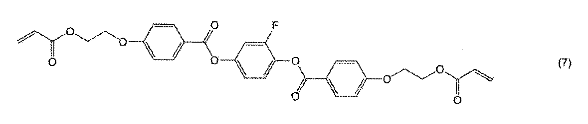
また、下記の構造式(8)で表す2官能のモノマーを用いて素子Eを作製した。なお、構造式(7)で表す材料および構造式(8)で表す多官能モノマーは、いずれも安息香酸フェニル骨格を備える。
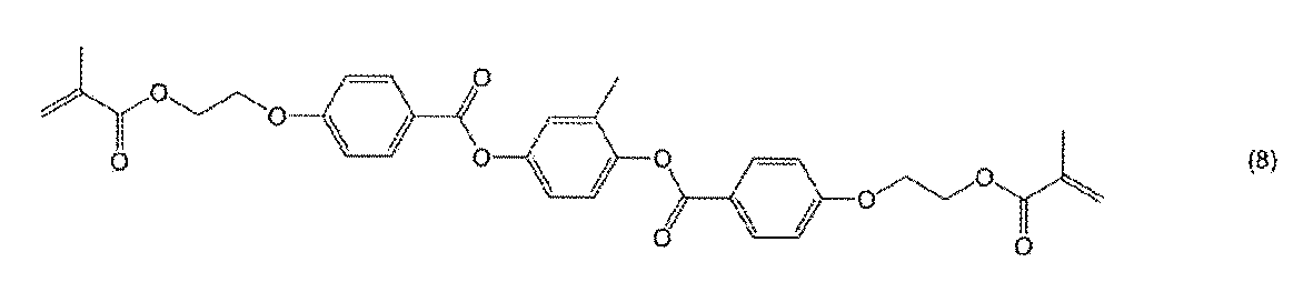
なお、構造式(1)で表す2官能のモノマーを用いて、比較例1の素子を作製し、構造式(7)で表す2官能のモノマーを用いて、比較例2の素子を作製した。
なお、表1において、符号LC−1は液晶材料(メルク社製:MDA−00−3506)に対応する。また、符号DM−1は構造式(1)で表す2官能のモノマーに対応し、符号DM−2は構造式(7)で表す2官能のモノマーに対応し、符号DM−3は構造式(8)で表す2官能のモノマーに対応する。また、符号MM−1は構造式(2)で表す単官能のモノマーに対応し、符号MM−2は構造式(3)で表す単官能のモノマーに対応し、符号MM−3は構造式(4)で表す単官能のモノマーに対応する。なお、液晶材料が92.5重量%、モノマーが7.5重量%になるように混合して用いた。
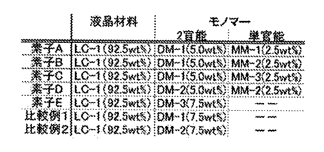
<評価方法>
作製した液晶素子の散乱強度、耐熱性およびコントラスト比について、以下の方法を用いて評価した。
作製した液晶素子の散乱強度、耐熱性およびコントラスト比について、以下の方法を用いて評価した。
《散乱強度の評価》
強度I0の光を、液晶素子75を通る垂線から30°傾けて、液晶素子75の一方の面に照射した(図1(A)参照)。また、散乱する光の強度Idを、対向する面の垂線方向において測定し、入射光の強度I0に対する散乱光の強度Idの割合(Id/I0)を散乱強度とした。なお、液晶素子を配置せず、検出器を光源と正対する位置に配置すると、当該検出器は入射光の強度I0を観測する。また、液晶素子75を通る垂線を軸にして、液晶素子75を回転しながら複数回測定し、当該複数の測定値を平均した値を、散乱光の強度Idに採用した(図1(B)参照)。なお、配向膜AF1に施したラビングの方向を基準に、当該方向に対する角度を方位角θと定義した。また、光源にはハロゲンランプを用いた。
強度I0の光を、液晶素子75を通る垂線から30°傾けて、液晶素子75の一方の面に照射した(図1(A)参照)。また、散乱する光の強度Idを、対向する面の垂線方向において測定し、入射光の強度I0に対する散乱光の強度Idの割合(Id/I0)を散乱強度とした。なお、液晶素子を配置せず、検出器を光源と正対する位置に配置すると、当該検出器は入射光の強度I0を観測する。また、液晶素子75を通る垂線を軸にして、液晶素子75を回転しながら複数回測定し、当該複数の測定値を平均した値を、散乱光の強度Idに採用した(図1(B)参照)。なお、配向膜AF1に施したラビングの方向を基準に、当該方向に対する角度を方位角θと定義した。また、光源にはハロゲンランプを用いた。
《耐熱性の評価》
液晶素子を120℃の環境で1時間保存する試験を行った。当該試験の前後に、液晶素子の散乱強度を評価し、比較した。
液晶素子を120℃の環境で1時間保存する試験を行った。当該試験の前後に、液晶素子の散乱強度を評価し、比較した。
《コントラスト比の評価》
液晶素子75を通る垂線から90°傾けて、光を液晶素子75の側面から照射した(図1(A)参照)。また、液晶素子75の面の垂線方向に散乱する光の強度を測定した。なお、電極51および電極52の間の電圧を、0.2Vステップで0Vから30Vまで上昇し、散乱する光の強度を各ステップで測定した。一群の測定値に含まれる、散乱光の強度Idの最小値Idminおよび最大値Idmaxの比の値(Idmax/Idmin)をコントラスト比と定義した。なお、本実施例で作製した液晶素子は、電極51および電極52の間の電圧が0Vの時に、散乱する光の強度Idは最小値Idminとなる。
液晶素子75を通る垂線から90°傾けて、光を液晶素子75の側面から照射した(図1(A)参照)。また、液晶素子75の面の垂線方向に散乱する光の強度を測定した。なお、電極51および電極52の間の電圧を、0.2Vステップで0Vから30Vまで上昇し、散乱する光の強度を各ステップで測定した。一群の測定値に含まれる、散乱光の強度Idの最小値Idminおよび最大値Idmaxの比の値(Idmax/Idmin)をコントラスト比と定義した。なお、本実施例で作製した液晶素子は、電極51および電極52の間の電圧が0Vの時に、散乱する光の強度Idは最小値Idminとなる。
<評価結果1.>
電極51および電極52の間に電圧を印加しない状態で、散乱強度を測定した結果を示す(図8参照)。
電極51および電極52の間に電圧を印加しない状態で、散乱強度を測定した結果を示す(図8参照)。
耐熱性試験前において、素子A、素子Bおよび素子Cは、比較例1の液晶素子より散乱強度が低かった。言い換えると、添加した単官能のモノマーが光の散乱を抑制し、液晶素子75の透明性を向上した。
120℃の環境で1時間保存する耐熱性試験後において、素子A、素子Bおよび素子Cは、比較例1の液晶素子より散乱強度が低かった。また、散乱強度の耐熱性試験に伴う変化が抑制されていた。言い換えると、添加した単官能のモノマーが、液晶素子75の信頼性を向上させた。
<評価結果2.>
作製した液晶素子のそれぞれについて、コントラスト比を測定した(図9参照)。素子A、素子Bおよび素子Cは、比較例1の液晶素子よりコントラスト比が高い。言い換えると、添加した単官能のモノマーが、液晶素子のコントラスト比を向上させた。
作製した液晶素子のそれぞれについて、コントラスト比を測定した(図9参照)。素子A、素子Bおよび素子Cは、比較例1の液晶素子よりコントラスト比が高い。言い換えると、添加した単官能のモノマーが、液晶素子のコントラスト比を向上させた。
<評価結果3.>
素子Dについて、散乱強度の入射光方位角に対する依存性を測定した(図10(A)参照)。耐熱性試験前の素子Dについての結果を素子D−1、耐熱性試験後の素子Dについての結果を素子D−2として示す。
素子Dについて、散乱強度の入射光方位角に対する依存性を測定した(図10(A)参照)。耐熱性試験前の素子Dについての結果を素子D−1、耐熱性試験後の素子Dについての結果を素子D−2として示す。
比較例2について、散乱強度の入射光方位角に対する依存性を測定した(図10(B)参照)。耐熱性試験前の比較例2についての結果を比較例2−1、耐熱性試験後の比較例2についての結果を比較例2−2として示す。
比較例2に比べて素子Dの散乱強度は小さい。また、比較例2に比べて素子Dの散乱強度の耐熱性試験に伴う変化も抑制されていた。言い換えると、添加した単官能のモノマーが液晶素子の信頼性を向上させた。
また、素子Eについても、散乱強度の入射光方位角に対する依存性を測定した(図11(A)参照)。耐熱性試験前の素子Eについての結果を素子E−1、耐熱性試験後の素子Eについての結果を素子E−2として示す。素子Eの散乱強度の耐熱性試験に伴う変化は小さい。
<評価結果4.>
素子D、素子E、比較例2について、散乱強度の電圧依存性を測定した(図11(B)参照)。散乱強度の飽和領域において、素子Dは比較例2と同程度光を散乱した。なお、電圧を印加してから散乱強度が飽和するまでの時間を応答速度とすると、素子Dの応答速度は2.4msec、素子Eの応答速度は2.0msecであった。
素子D、素子E、比較例2について、散乱強度の電圧依存性を測定した(図11(B)参照)。散乱強度の飽和領域において、素子Dは比較例2と同程度光を散乱した。なお、電圧を印加してから散乱強度が飽和するまでの時間を応答速度とすると、素子Dの応答速度は2.4msec、素子Eの応答速度は2.0msecであった。
<評価結果5.>
所定の形状を備える導電膜を電極51に用いた液晶素子を作製した。電極51および電極52の間に電圧を印加しない状態を図12(A)に示し、15Vの電圧を印加した状態を図12(B)に示した。なお、液晶素子の側面にLEDを配置して、青色の光を照射した。入射した光は電極51の形状に応じて散乱し、透明な領域の中に文字を表示できた。
所定の形状を備える導電膜を電極51に用いた液晶素子を作製した。電極51および電極52の間に電圧を印加しない状態を図12(A)に示し、15Vの電圧を印加した状態を図12(B)に示した。なお、液晶素子の側面にLEDを配置して、青色の光を照射した。入射した光は電極51の形状に応じて散乱し、透明な領域の中に文字を表示できた。
なお、本実施例は、本明細書で示す他の実施の形態と適宜組み合わせることができる。
本実施例では、作製した本発明の一態様の表示装置の構成と評価結果について、図13乃至図17を参照しながら説明する。
図13は本発明の一態様の表示パネルの構成を説明する図である。図13(A)は本発明の一態様の表示パネルの画素の上面図であり、図13(B)は画素回路および表示素子の回路図である。
図14は本発明の一態様の表示パネルの透過率の波長依存性を説明する図である。
図15は本発明の一態様の表示パネルの表示性能を説明する図である。
図16は本発明の一態様の液晶素子の特性を説明する図である。図16(A)は本発明の一態様の液晶素子の散乱強度の印加電圧依存性を説明する特性曲線であり、図16(B)は本発明の一態様の液晶素子の表示特性を説明する図である。
図17は本発明の一態様の液晶素子に用いる液晶材料を含む層の誘電率の印加電圧依存性を説明する図である。
図18は本発明の一態様の表示パネルの表示性能を説明する図である。図18(A−1)、図18(B−1)および図18(C−1)は、画像信号のみを用いて表示をした結果を説明する写真であり、図18(A−2)、図18(B−2)および図18(C−2)は、画像信号および制御信号を用いて表示をした結果を説明する写真である。
<作製した表示装置の構成>
表示装置は、表示パネルおよび光源を有する。
表示装置は、表示パネルおよび光源を有する。
《表示装置の構成》
作製した表示装置の仕様を表2に示す。
作製した表示装置の仕様を表2に示す。
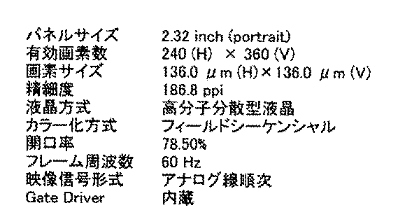
周波数が37.31kHzの信号をクロック信号に用いて、駆動回路GDを動作した。また、駆動回路GDは、電圧が−35Vの信号と、電圧が+20Vの信号を供給することができた。
なお、導電膜VCOM1の電位を−15Vと+15Vになるように制御して、表示素子750(i,j)に加える電圧を反転した。
1水平期間を6.7μsecにして、駆動回路SDを動作した。また、駆動回路SDは、電圧が−9Vの信号と、+9Vの信号を供給することができた。
作製した表示パネルの透過率は、波長550nm付近で約62%であった。
<表示結果>
作製した表示装置に画像Image1を表示した(図15参照)。なお、表示領域231内に見える画像Image2は、表示パネルの向こう側に重ねて配置した印刷物の外観である。言い換えると、画像Image2は、表示領域231の透明な部分を透過して見える印刷物の外観である。
作製した表示装置に画像Image1を表示した(図15参照)。なお、表示領域231内に見える画像Image2は、表示パネルの向こう側に重ねて配置した印刷物の外観である。言い換えると、画像Image2は、表示領域231の透明な部分を透過して見える印刷物の外観である。
液晶素子に加える電圧の最大値が9Vになるように、画像信号のみを用いて、3つの異なる画像を表示した(図18(A−1)、図18(B−1)および図18(C−1)参照)。
また、液晶素子に加える電圧の最大値が16.7Vになるように、画像信号および制御信号を用いて、3つの異なる画像を表示した(図18(A−2)、図18(B−2)および図18(C−2)参照)。なお、図18(A−2)は図18(A−1)に表示した画像信号に制御信号を加えた表示であり、図18(B−2)は図18(B−1)に表示した画像信号に制御信号を加えた表示であり、図18(C−2)は図18(C−1)に表示した画像信号に制御信号を加えた表示である。
画像信号および制御信号を用いることにより、コントラスト比を高めることができた。
<作製した液晶素子の特性>
4μmのセルギャップを備える液晶素子を作製し、散乱強度の印加電圧依存性を測定した(図16(A)参照)。液晶素子はリバースモードで動作した。
4μmのセルギャップを備える液晶素子を作製し、散乱強度の印加電圧依存性を測定した(図16(A)参照)。液晶素子はリバースモードで動作した。
作製した液晶素子に256階調の信号を表示した(図16(B)参照)。オフセットするための所定の電圧を256階調の信号に加えて表示すると、256階調の信号のみを液晶素子に表示する場合に比べて、散乱強度を高めることができた。その結果、エッジライトを用いて表示パネルの側面から入射した光を、表示パネルの正面方向等に散乱し、正面の輝度を高めることができた。
作製した液晶素子の容量の印加電圧依存性を測定し、液晶材料を含む層の誘電率の印加電圧依存性を算出した(図17参照)。なお、繰り返して測定した結果はよく一致した。
本実施例では、作製した本発明の一態様の液晶素子の構成と評価結果について、図1および図19を参照しながら説明する。
<作製した液晶素子の構成>
無アルカリガラスを基材に用いた。基材上に形成した透明導電膜を電極に用いた。一の基材上の電極51上に配向膜AF1を形成し、他の基材上の電極52上に配向膜AF2を形成した。なお、配向膜AF1を水平方向に配向するようにラビングし、配向膜AF1に対してアンチパラレルに配向するように配向膜AF2をラビングした。
無アルカリガラスを基材に用いた。基材上に形成した透明導電膜を電極に用いた。一の基材上の電極51上に配向膜AF1を形成し、他の基材上の電極52上に配向膜AF2を形成した。なお、配向膜AF1を水平方向に配向するようにラビングし、配向膜AF1に対してアンチパラレルに配向するように配向膜AF2をラビングした。
液晶材料、多官能モノマーおよび単官能モノマーを含む組成物を、電極51および電極52の間に封止材を用いて封止し、液晶材料を含む層53を高分子安定化した。具体的には、当該組成物に紫外線を照射して、液晶材料を含む層53を形成した。なお、液晶材料を含む層53の厚さが4.0μmになるように、セルギャップを設け、30℃、40℃、50℃の3つの異なる温度で形成した。
《液晶材料を含む層の構成》
液晶材料を含む層53の構成が異なる9種類の素子を作製した(表3参照)。具体的には、構造式(4)で表す単官能のモノマーと、構造式(9)で表す2官能のモノマーを混合して、素子F1乃至素子F3、素子G1乃至素子G3、素子H1乃至素子H3を作製した。作製した素子は、例えば、液晶材料を含む層を形成する際に用いた組成物のモノマーの混合比が異なる。または、組成物を高分子安定化した際の温度が異なる。
液晶材料を含む層53の構成が異なる9種類の素子を作製した(表3参照)。具体的には、構造式(4)で表す単官能のモノマーと、構造式(9)で表す2官能のモノマーを混合して、素子F1乃至素子F3、素子G1乃至素子G3、素子H1乃至素子H3を作製した。作製した素子は、例えば、液晶材料を含む層を形成する際に用いた組成物のモノマーの混合比が異なる。または、組成物を高分子安定化した際の温度が異なる。
なお、表3において、符号DM−4は構造式(9)で表す2官能のモノマーに対応する。また、構造式(10)で表す重合開始剤を高分子安定化に用いた。重合開始剤の添加量は、上記組成物の0.1重量%であった。


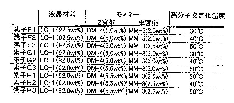
<評価結果>
素子F1乃至F3、素子G1乃至G3、素子H1乃至H3について、コントラスト比を測定した(図19参照)。いずれの素子もコントラスト比が25以上と大きい結果となった。素子H1乃至素子H3はコントラスト比が高いだけでなく高分子安定化時の温度依存性が小さかった。
素子F1乃至F3、素子G1乃至G3、素子H1乃至H3について、コントラスト比を測定した(図19参照)。いずれの素子もコントラスト比が25以上と大きい結果となった。素子H1乃至素子H3はコントラスト比が高いだけでなく高分子安定化時の温度依存性が小さかった。
本実施例では、作製した本発明の一態様の液晶素子の構成と評価結果について、図1および図20を参照しながら説明する。なお、本実施例で作成した液晶素子は、液晶材料を含む層53の構成が、実施例3とは異なる。具体的には、液晶材料を含む層を形成する際に、実施例3とは異なる2官能のモノマーを用いた。ここでは、異なる部分について詳細に説明し、同様の構成を用いることができる部分について上記の説明を援用する。
《液晶材料を含む層の構成》
液晶材料を含む層53の構成が異なる6種類の素子を作製した(表4参照)。具体的には、構造式(4)で表す単官能のモノマーと、構造式(11)で表す2官能のモノマーを混合して、素子I1乃至素子I3、素子J1乃至素子J3を作製した。作製した素子は、例えば、液晶材料を含む層を形成する際に用いた組成物のモノマーの混合比が異なる。または、組成物を高分子安定化した際の温度が異なる。
液晶材料を含む層53の構成が異なる6種類の素子を作製した(表4参照)。具体的には、構造式(4)で表す単官能のモノマーと、構造式(11)で表す2官能のモノマーを混合して、素子I1乃至素子I3、素子J1乃至素子J3を作製した。作製した素子は、例えば、液晶材料を含む層を形成する際に用いた組成物のモノマーの混合比が異なる。または、組成物を高分子安定化した際の温度が異なる。
なお、表4において、符号DM−5は構造式(11)で表す2官能のモノマーに対応する。


<評価結果>
素子I1乃至素子I3、素子J1乃至素子J3について、コントラスト比を測定した(図20参照)。いずれの素子もコントラスト比が30以上と大きい結果となった。特に素子J2はコントラスト比が40以上と高い結果となった。
素子I1乃至素子I3、素子J1乃至素子J3について、コントラスト比を測定した(図20参照)。いずれの素子もコントラスト比が30以上と大きい結果となった。特に素子J2はコントラスト比が40以上と高い結果となった。
なお、本実施例は、本明細書で示す他の実施の形態と適宜組み合わせることができる。
例えば、本明細書等において、XとYとが接続されている、と明示的に記載されている場合は、XとYとが電気的に接続されている場合と、XとYとが機能的に接続されている場合と、XとYとが直接接続されている場合とが、本明細書等に開示されているものとする。したがって、所定の接続関係、例えば、図または文章に示された接続関係に限定されず、図または文章に示された接続関係以外のものも、図または文章に開示されているものとする。
ここで、X、Yは、対象物(例えば、装置、素子、回路、配線、電極、端子、導電膜、層、など)であるとする。
XとYとが直接的に接続されている場合の一例としては、XとYとの電気的な接続を可能とする素子(例えば、スイッチ、トランジスタ、容量素子、インダクタ、抵抗素子、ダイオード、表示素子、発光素子、負荷など)が、XとYとの間に接続されていない場合であり、XとYとの電気的な接続を可能とする素子(例えば、スイッチ、トランジスタ、容量素子、インダクタ、抵抗素子、ダイオード、表示素子、発光素子、負荷など)を介さずに、XとYとが、接続されている場合である。
XとYとが電気的に接続されている場合の一例としては、XとYとの電気的な接続を可能とする素子(例えば、スイッチ、トランジスタ、容量素子、インダクタ、抵抗素子、ダイオード、表示素子、発光素子、負荷など)が、XとYとの間に1個以上接続されることが可能である。なお、スイッチは、オンオフが制御される機能を有している。つまり、スイッチは、導通状態(オン状態)、または、非導通状態(オフ状態)になり、電流を流すか流さないかを制御する機能を有している。または、スイッチは、電流を流す経路を選択して切り替える機能を有している。なお、XとYとが電気的に接続されている場合は、XとYとが直接的に接続されている場合を含むものとする。
XとYとが機能的に接続されている場合の一例としては、XとYとの機能的な接続を可能とする回路(例えば、論理回路(インバータ、NAND回路、NOR回路など)、信号変換回路(DA変換回路、AD変換回路、ガンマ補正回路など)、電位レベル変換回路(電源回路(昇圧回路、降圧回路など)、信号の電位レベルを変えるレベルシフタ回路など)、電圧源、電流源、切り替え回路、増幅回路(信号振幅または電流量などを大きく出来る回路、オペアンプ、差動増幅回路、ソースフォロワ回路、バッファ回路など)、信号生成回路、記憶回路、制御回路など)が、XとYとの間に1個以上接続されることが可能である。なお、一例として、XとYとの間に別の回路を挟んでいても、Xから出力された信号がYへ伝達される場合は、XとYとは機能的に接続されているものとする。なお、XとYとが機能的に接続されている場合は、XとYとが直接的に接続されている場合と、XとYとが電気的に接続されている場合とを含むものとする。
なお、XとYとが電気的に接続されている、と明示的に記載されている場合は、XとYとが電気的に接続されている場合(つまり、XとYとの間に別の素子又は別の回路を挟んで接続されている場合)と、XとYとが機能的に接続されている場合(つまり、XとYとの間に別の回路を挟んで機能的に接続されている場合)と、XとYとが直接接続されている場合(つまり、XとYとの間に別の素子又は別の回路を挟まずに接続されている場合)とが、本明細書等に開示されているものとする。つまり、電気的に接続されている、と明示的に記載されている場合は、単に、接続されている、とのみ明示的に記載されている場合と同様な内容が、本明細書等に開示されているものとする。
なお、例えば、トランジスタのソース(又は第1の端子など)が、Z1を介して(又は介さず)、Xと電気的に接続され、トランジスタのドレイン(又は第2の端子など)が、Z2を介して(又は介さず)、Yと電気的に接続されている場合や、トランジスタのソース(又は第1の端子など)が、Z1の一部と直接的に接続され、Z1の別の一部がXと直接的に接続され、トランジスタのドレイン(又は第2の端子など)が、Z2の一部と直接的に接続され、Z2の別の一部がYと直接的に接続されている場合では、以下のように表現することが出来る。
例えば、「XとYとトランジスタのソース(又は第1の端子など)とドレイン(又は第2の端子など)とは、互いに電気的に接続されており、X、トランジスタのソース(又は第1の端子など)、トランジスタのドレイン(又は第2の端子など)、Yの順序で電気的に接続されている。」と表現することができる。または、「トランジスタのソース(又は第1の端子など)は、Xと電気的に接続され、トランジスタのドレイン(又は第2の端子など)はYと電気的に接続され、X、トランジスタのソース(又は第1の端子など)、トランジスタのドレイン(又は第2の端子など)、Yは、この順序で電気的に接続されている」と表現することができる。または、「Xは、トランジスタのソース(又は第1の端子など)とドレイン(又は第2の端子など)とを介して、Yと電気的に接続され、X、トランジスタのソース(又は第1の端子など)、トランジスタのドレイン(又は第2の端子など)、Yは、この接続順序で設けられている」と表現することができる。これらの例と同様な表現方法を用いて、回路構成における接続の順序について規定することにより、トランジスタのソース(又は第1の端子など)と、ドレイン(又は第2の端子など)とを、区別して、技術的範囲を決定することができる。
または、別の表現方法として、例えば、「トランジスタのソース(又は第1の端子など)は、少なくとも第1の接続経路を介して、Xと電気的に接続され、前記第1の接続経路は、第2の接続経路を有しておらず、前記第2の接続経路は、トランジスタを介した、トランジスタのソース(又は第1の端子など)とトランジスタのドレイン(又は第2の端子など)との間の経路であり、前記第1の接続経路は、Z1を介した経路であり、トランジスタのドレイン(又は第2の端子など)は、少なくとも第3の接続経路を介して、Yと電気的に接続され、前記第3の接続経路は、前記第2の接続経路を有しておらず、前記第3の接続経路は、Z2を介した経路である。」と表現することができる。または、「トランジスタのソース(又は第1の端子など)は、少なくとも第1の接続経路によって、Z1を介して、Xと電気的に接続され、前記第1の接続経路は、第2の接続経路を有しておらず、前記第2の接続経路は、トランジスタを介した接続経路を有し、トランジスタのドレイン(又は第2の端子など)は、少なくとも第3の接続経路によって、Z2を介して、Yと電気的に接続され、前記第3の接続経路は、前記第2の接続経路を有していない。」と表現することができる。または、「トランジスタのソース(又は第1の端子など)は、少なくとも第1の電気的パスによって、Z1を介して、Xと電気的に接続され、前記第1の電気的パスは、第2の電気的パスを有しておらず、前記第2の電気的パスは、トランジスタのソース(又は第1の端子など)からトランジスタのドレイン(又は第2の端子など)への電気的パスであり、トランジスタのドレイン(又は第2の端子など)は、少なくとも第3の電気的パスによって、Z2を介して、Yと電気的に接続され、前記第3の電気的パスは、第4の電気的パスを有しておらず、前記第4の電気的パスは、トランジスタのドレイン(又は第2の端子など)からトランジスタのソース(又は第1の端子など)への電気的パスである。」と表現することができる。これらの例と同様な表現方法を用いて、回路構成における接続経路について規定することにより、トランジスタのソース(又は第1の端子など)と、ドレイン(又は第2の端子など)とを、区別して、技術的範囲を決定することができる。
なお、これらの表現方法は、一例であり、これらの表現方法に限定されない。ここで、X、Y、Z1、Z2は、対象物(例えば、装置、素子、回路、配線、電極、端子、導電膜、層、など)であるとする。
なお、回路図上は独立している構成要素同士が電気的に接続しているように図示されている場合であっても、1つの構成要素が、複数の構成要素の機能を併せ持っている場合もある。例えば配線の一部が電極としても機能する場合は、一の導電膜が、配線の機能、及び電極の機能の両方の構成要素の機能を併せ持っている。したがって、本明細書における電気的に接続とは、このような、一の導電膜が、複数の構成要素の機能を併せ持っている場合も、その範疇に含める。
AF1:配向膜、AF2:配向膜、C11:容量素子、C12:容量素子、CI:制御情報、G1(i):走査線、GD:駆動回路、GDA:駆動回路、GDB:駆動回路、KB1:構造体、MG1:トランジスタ、S1:信号線、SD:駆動回路、SDA(1):駆動回路、SDA(2):駆動回路、SDB(1):駆動回路、SDB(2):駆動回路、SDC(1):駆動回路、SDC(2):駆動回路、SP:制御信号、SW1:スイッチ、SW12:スイッチ、V1:画像情報、V11:情報、VCOM1:導電膜、50:液晶素子、51:電極、52:電極、53:液晶材料を含む層、75:液晶素子、231:表示領域、233:制御回路、234:伸張回路、235:画像処理回路、238:制御部、501C:絶縁膜、501D:絶縁膜、504:導電膜、506:絶縁膜、508:半導体膜、508A:領域、508B:領域、508C:領域、510:基材、512A:導電膜、512B:導電膜、516:絶縁膜、516A:絶縁膜、516B:絶縁膜、518:絶縁膜、520:機能層、521A:絶縁膜、524:導電膜、530:画素回路、591A:開口部、700:表示パネル、702:画素、705:封止材、750:表示素子、751:電極、752:電極、753:液晶材料を含む層、770:基材、770P:機能膜
Claims (5)
- 第1の電極と、
第2の電極と、
液晶材料を含む層と、
第1の配向膜と、
第2の配向膜と、を有し、
前記第1の配向膜は、前記第1の電極および前記液晶材料を含む層の間に挟まれる領域を備え、
前記第2の配向膜は、前記第2の電極および前記液晶材料を含む層の間に挟まれる領域を備え、
前記第2の電極は、前記第1の電極との間に、前記液晶材料を含む層を横切る電界を形成するように配置され、
前記液晶材料を含む層は、前記電界が第1の状態において、入射光を第1の散乱強度で散乱し、
前記液晶材料を含む層は、前記電界が第1の状態より大きい第2の状態において、前記入射光を第2の散乱強度で散乱し、
前記第2の散乱強度は、第1の散乱強度より大きく、
前記液晶材料を含む層は、液晶材料および高分子材料を含み、
前記液晶材料を含む層は、前記高分子で安定化され、
前記高分子材料は、多官能モノマーおよび単官能モノマーの共重合体であり、
前記多官能モノマーは、安息香酸フェニル骨格を備え、
前記単官能モノマーは、シクロヘキシルベンゼン骨格を備える、液晶素子。 - 前記第2の散乱強度は、前記第1の散乱強度の10倍以上である、請求項1に記載の液晶素子。
- 画素を有し、
前記画素は、前記画素回路および請求項1または請求項2に記載の液晶素子を備え、
前記液晶素子は、前記画素回路と電気的に接続される、表示パネル。 - 表示領域を有し、
前記表示領域は、一群の画素、他の一群の画素、走査線および信号線を備え、
前記一群の画素は、前記画素を含み、
前記一群の画素は、行方向に配設され、
前記他の一群の画素は、前記画素を含み、
前記他の一群の画素は、行方向と交差する列方向に配設され、
前記走査線は、前記一群の画素と電気的に接続され、
前記信号線は、前記他の一群の画素と電気的に接続される、請求項3に記載の表示パネル。 - 請求項3または請求項4のいずれかに記載の表示パネルと、
制御部と、を有し、
前記制御部は、画像情報および制御情報が供給され、
前記制御部は、前記画像情報に基づいて情報を生成し、
前記制御部は、前記制御情報にもとづいて制御信号を生成し、
前記制御部は、前記情報および制御信号を供給し、
前記表示パネルは、前記情報および前記制御信号が供給され、
前記表示パネルは、駆動回路を備え、
前記駆動回路は、前記制御信号に基づいて動作し、
前記画素は、前記情報に基づいて表示する、表示装置。
Applications Claiming Priority (8)
| Application Number | Priority Date | Filing Date | Title |
|---|---|---|---|
| JP2018096512 | 2018-05-18 | ||
| JP2018-096512 | 2018-05-18 | ||
| JP2018105088 | 2018-05-31 | ||
| JP2018-105088 | 2018-05-31 | ||
| JP2018-150750 | 2018-08-09 | ||
| JP2018150750 | 2018-08-09 | ||
| JP2018159170 | 2018-08-28 | ||
| JP2018-159170 | 2018-08-28 |
Publications (1)
| Publication Number | Publication Date |
|---|---|
| WO2019220299A1 true WO2019220299A1 (ja) | 2019-11-21 |
Family
ID=68539986
Family Applications (1)
| Application Number | Title | Priority Date | Filing Date |
|---|---|---|---|
| PCT/IB2019/053911 Ceased WO2019220299A1 (ja) | 2018-05-18 | 2019-05-13 | 液晶素子、表示パネル、表示装置 |
Country Status (1)
| Country | Link |
|---|---|
| WO (1) | WO2019220299A1 (ja) |
Citations (4)
| Publication number | Priority date | Publication date | Assignee | Title |
|---|---|---|---|---|
| JP2008058374A (ja) * | 2006-08-29 | 2008-03-13 | Dainippon Ink & Chem Inc | 液晶素子 |
| WO2017217430A1 (ja) * | 2016-06-14 | 2017-12-21 | 三菱ケミカル株式会社 | 液晶素子、液晶組成物並びに液晶素子を用いたスクリーン、ディスプレイ及び窓 |
| WO2018025996A1 (ja) * | 2016-08-04 | 2018-02-08 | Jnc株式会社 | 液晶デバイス用材料および液晶デバイス |
| WO2018043276A1 (ja) * | 2016-08-30 | 2018-03-08 | Dic株式会社 | 液晶素子 |
-
2019
- 2019-05-13 WO PCT/IB2019/053911 patent/WO2019220299A1/ja not_active Ceased
Patent Citations (4)
| Publication number | Priority date | Publication date | Assignee | Title |
|---|---|---|---|---|
| JP2008058374A (ja) * | 2006-08-29 | 2008-03-13 | Dainippon Ink & Chem Inc | 液晶素子 |
| WO2017217430A1 (ja) * | 2016-06-14 | 2017-12-21 | 三菱ケミカル株式会社 | 液晶素子、液晶組成物並びに液晶素子を用いたスクリーン、ディスプレイ及び窓 |
| WO2018025996A1 (ja) * | 2016-08-04 | 2018-02-08 | Jnc株式会社 | 液晶デバイス用材料および液晶デバイス |
| WO2018043276A1 (ja) * | 2016-08-30 | 2018-03-08 | Dic株式会社 | 液晶素子 |
Similar Documents
| Publication | Publication Date | Title |
|---|---|---|
| US12008975B2 (en) | Display device and operating method thereof | |
| US11048111B2 (en) | Display device equipped touch panel | |
| TWI753908B (zh) | 半導體裝置、顯示裝置及電子裝置 | |
| JP2023099595A (ja) | 電子機器 | |
| US10453866B2 (en) | Semiconductor device and electronic device | |
| CN102971784A (zh) | 液晶显示装置及驱动液晶显示装置的方法 | |
| CN111433838A (zh) | 显示装置及电子设备 | |
| JP7433493B2 (ja) | 表示パネル | |
| JP7109887B2 (ja) | 表示システム | |
| JP7814566B2 (ja) | 半導体装置 | |
| US7847895B2 (en) | Liquid crystal display device | |
| US20180090111A1 (en) | Semiconductor device, method for operating the same, and electronic device | |
| US9780779B2 (en) | Semiconductor device, electronic component, and electronic device | |
| JP7010628B2 (ja) | 表示装置および電子機器 | |
| JP2018049268A (ja) | 表示パネル、表示装置、入出力装置、情報処理装置、表示パネルの作製方法 | |
| JP7044495B2 (ja) | 半導体装置 | |
| KR102887409B1 (ko) | 표시 장치, 표시 모듈, 및 전자 기기 | |
| WO2020039292A1 (ja) | 表示パネル、表示装置 | |
| CN1938748A (zh) | 液晶显示装置以及其驱动方法 |
Legal Events
| Date | Code | Title | Description |
|---|---|---|---|
| 121 | Ep: the epo has been informed by wipo that ep was designated in this application |
Ref document number: 19802708 Country of ref document: EP Kind code of ref document: A1 |
|
| NENP | Non-entry into the national phase |
Ref country code: DE |
|
| 122 | Ep: pct application non-entry in european phase |
Ref document number: 19802708 Country of ref document: EP Kind code of ref document: A1 |
|
| NENP | Non-entry into the national phase |
Ref country code: JP |