WO2019214079A1 - 一种TiO2纳米柱-Au纳米粒子复合阵列、制备方法及其应用 - Google Patents
一种TiO2纳米柱-Au纳米粒子复合阵列、制备方法及其应用 Download PDFInfo
- Publication number
- WO2019214079A1 WO2019214079A1 PCT/CN2018/096920 CN2018096920W WO2019214079A1 WO 2019214079 A1 WO2019214079 A1 WO 2019214079A1 CN 2018096920 W CN2018096920 W CN 2018096920W WO 2019214079 A1 WO2019214079 A1 WO 2019214079A1
- Authority
- WO
- WIPO (PCT)
- Prior art keywords
- tio
- nanocolumn
- composite array
- nanoparticle
- nanoparticle composite
- Prior art date
- Legal status (The legal status is an assumption and is not a legal conclusion. Google has not performed a legal analysis and makes no representation as to the accuracy of the status listed.)
- Ceased
Links
Images


Classifications
-
- H—ELECTRICITY
- H10—SEMICONDUCTOR DEVICES; ELECTRIC SOLID-STATE DEVICES NOT OTHERWISE PROVIDED FOR
- H10K—ORGANIC ELECTRIC SOLID-STATE DEVICES
- H10K30/00—Organic devices sensitive to infrared radiation, light, electromagnetic radiation of shorter wavelength or corpuscular radiation
- H10K30/10—Organic devices sensitive to infrared radiation, light, electromagnetic radiation of shorter wavelength or corpuscular radiation comprising heterojunctions between organic semiconductors and inorganic semiconductors
- H10K30/15—Sensitised wide-bandgap semiconductor devices, e.g. dye-sensitised TiO2
- H10K30/151—Sensitised wide-bandgap semiconductor devices, e.g. dye-sensitised TiO2 the wide bandgap semiconductor comprising titanium oxide, e.g. TiO2
-
- B—PERFORMING OPERATIONS; TRANSPORTING
- B82—NANOTECHNOLOGY
- B82Y—SPECIFIC USES OR APPLICATIONS OF NANOSTRUCTURES; MEASUREMENT OR ANALYSIS OF NANOSTRUCTURES; MANUFACTURE OR TREATMENT OF NANOSTRUCTURES
- B82Y30/00—Nanotechnology for materials or surface science, e.g. nanocomposites
-
- B—PERFORMING OPERATIONS; TRANSPORTING
- B82—NANOTECHNOLOGY
- B82Y—SPECIFIC USES OR APPLICATIONS OF NANOSTRUCTURES; MEASUREMENT OR ANALYSIS OF NANOSTRUCTURES; MANUFACTURE OR TREATMENT OF NANOSTRUCTURES
- B82Y40/00—Manufacture or treatment of nanostructures
-
- H—ELECTRICITY
- H10—SEMICONDUCTOR DEVICES; ELECTRIC SOLID-STATE DEVICES NOT OTHERWISE PROVIDED FOR
- H10K—ORGANIC ELECTRIC SOLID-STATE DEVICES
- H10K30/00—Organic devices sensitive to infrared radiation, light, electromagnetic radiation of shorter wavelength or corpuscular radiation
- H10K30/80—Constructional details
- H10K30/81—Electrodes
- H10K30/82—Transparent electrodes, e.g. indium tin oxide [ITO] electrodes
-
- Y—GENERAL TAGGING OF NEW TECHNOLOGICAL DEVELOPMENTS; GENERAL TAGGING OF CROSS-SECTIONAL TECHNOLOGIES SPANNING OVER SEVERAL SECTIONS OF THE IPC; TECHNICAL SUBJECTS COVERED BY FORMER USPC CROSS-REFERENCE ART COLLECTIONS [XRACs] AND DIGESTS
- Y02—TECHNOLOGIES OR APPLICATIONS FOR MITIGATION OR ADAPTATION AGAINST CLIMATE CHANGE
- Y02E—REDUCTION OF GREENHOUSE GAS [GHG] EMISSIONS, RELATED TO ENERGY GENERATION, TRANSMISSION OR DISTRIBUTION
- Y02E10/00—Energy generation through renewable energy sources
- Y02E10/50—Photovoltaic [PV] energy
- Y02E10/549—Organic PV cells
Definitions
- the invention belongs to the field of nano materials and relates to a composite array, in particular to a preparation method and application of a TiO 2 nano column-Au nano particle composite array.
- Precious metal nanostructures with surface plasmon resonance effects have been developed into an effective way to effectively improve the performance of various light collection system devices, and have important application value in photovoltaic devices such as solar cells, photocatalysis, photolysis water and photodetectors.
- Precious metal nanostructures concentrate light in the nanoscale range near the surface of the nanostructure, producing a strong local surface plasmon resonance effect.
- Precious metals such as gold, silver and platinum are metal materials commonly used for surface plasmon resonance.
- PSCs polymer solar cells
- the carrier semiconductor mobility of the polymer semiconductor material constituting the active layer is low, and in order to reduce the internal recombination of carriers in the battery, it is generally required to limit the thickness of the active layer to ⁇ 100 to 200 nm.
- the thickness of the active layer is too thin, the absorption capacity of the incident light is insufficient, the utilization of the incident light is lowered, and the photoelectric conversion efficiency of the battery is seriously limited.
- Reasonable utilization of the surface plasmon resonance effect of the metal nanostructure can increase the light absorption level without increasing the thickness of the active layer, thereby avoiding the internal recombination of electrons and holes due to the increase in the thickness of the active layer, and further improving the battery performance.
- the object of the present invention is to provide a TiO 2 nanocolumn-Au nanoparticle composite array in order to overcome the deficiencies of the prior art.
- the technical solution adopted by the present invention is: a TiO 2 nanocolumn-Au nanoparticle composite array comprising a plurality of TiO 2 nanocolumns formed on a surface of a substrate and formed at a free end of the TiO 2 nanocolumn Au nanoparticles.
- the TiO 2 nanocolumn has a diameter of 20 to 60 nm and a height of 20 to 100 nm; and the Au nanoparticle has a particle diameter of 20 to 60 nm.
- the substrate is ITO glass, FTO glass, silicon wafer or glass.
- Another object of the present invention is to provide a method for preparing the above TiO 2 nanocolumn-Au nanoparticle composite array, which comprises the following steps:
- the Au nanoparticle array is supported on the surface of the TiO 2 nanofilm by a self-assembly method or an evaporation method, and then etched by using a mixed gas of CHF 3 and argon as an etching gas.
- step (a) comprises the steps of:
- the TiO 2 sol is dropped onto the surface of the treated substrate, spin-coated to obtain a uniform wet film, and further heat-treated at 250 to 500 ° C to obtain a TiO 2 nano film.
- the self-assembly method comprises the following steps:
- the product in the step (11) is immersed in the gold nanoparticle solution, allowed to stand for 2 to 6 hours, taken out, rinsed with water, and dried.
- the evaporation method comprises the following steps:
- the product in the step (21) may be heated at 250 to 350 °C.
- a further object of the present invention is to provide an application of the above TiO 2 nanocolumn-Au nanoparticle composite array, characterized in that the TiO 2 nanocolumn-Au nanoparticle composite array is used as a cathode buffer layer of an organic solar cell. .
- the present invention has the following advantages compared with the prior art: the TiO 2 nanocolumn-Au nanoparticle composite array of the present invention, the TiO 2 nanocolumn is formed by forming Au nanoparticles at the free end of the TiO 2 nanocolumn.
- the preparation density is controllable, the height is adjustable, and the particle size of Au nanoparticles is controllable, and the surface plasmon resonance property in the visible light region can be obtained, and the spatial distribution state of the gold nanoparticles can be regulated by the titanium dioxide nanocolumn, which is better used for Enhance the energy conversion efficiency of photovoltaic devices such as solar cells, photolysis water, and photocatalysis; and the preparation method has the advantages of good repeatability and large area preparation.
- Example 1 is an SEM image of the product of Example 1: (a) Au nanoparticles were assembled by 2h; (b) Au nanoparticles were assembled by 4h; (c) Au nanoparticles were assembled by 6h; (d) 2h assembly TiO 2 nano-column-Au nanoparticle composite array obtained after etching; (e) TiO 2 nano-column-Au nano-particle composite array obtained after 4h assembly; (f) 6h assembled and etched The obtained TiO 2 nanocolumn-Au nanoparticle composite array;
- Example 2 is an SEM image of a TiO 2 nanocolumn-Au nanoparticle composite array in Example 1: (a) a perspective view; (b) a cross-sectional view;
- Example 3 is an SEM image of the product in Example 2: (a) preparing Au nanoparticles by evaporation; (b) TiO 2 nanocolumn-Au nanoparticle composite array obtained after etching;
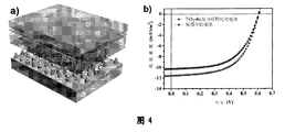
- Example 4 is a view showing the application of the product in Example 1: (a) Schematic diagram of the structure of the organic solar cell in Example 1; (b) Comparison of the performance of the organic solar cell in Example 1 and Comparative Example 1.
- the TiO 2 nanocolumn-Au nanoparticle composite array of the present invention comprises a plurality of TiO 2 nanocolumns formed on the surface of the substrate and Au nanoparticles formed at the free ends of the TiO 2 nanocolumns.
- the diameter of the TiO 2 nano-column is preferably 20-60 nm, and the height is preferably 20-100 nm (the height of the TiO 2 nano-column is smaller than the thickness of the TiO 2 nano-film described below, to avoid leakage of the substrate when the substrate is exposed during subsequent etching);
- the particle diameter of the Au nanoparticles is preferably 20 to 60 nm.
- the above substrate is usually a conductive material such as ITO glass, FTO glass, silicon wafer or glass.
- the free end of the Au nanoparticles TiO 2 nano-columns, such that the density of TiO 2 Nano controllable column, height-adjustable and controllable diameter Au nanoparticles, surface plasmon resonance properties can be obtained in the visible region, and
- the spatial distribution of gold nanoparticles can be controlled by titanium dioxide nanocolumns, which is better used to enhance the energy conversion efficiency of photovoltaic devices such as solar cells, photolysis water and photocatalysis; and the preparation method has good repeatability and large area preparation. advantage.
- the preparation method of the above TiO 2 nanocolumn-Au nanoparticle composite array comprises the steps of: (a) forming a TiO 2 nano film on the surface of the substrate; (b) using the self-assembly method or the evaporation method on the TiO 2 nano film.
- the Au nanoparticle array is surface-loaded, and then etched by using a mixed gas of CHF 3 and argon as an etching gas.
- the above step (a) comprises the steps of: (a1) adding bis(acetylacetonyl)diisopropyl titanate to a mixed solvent of n-butanol and isopropanol, and magnetically stirring at 40 to 60 ° C to obtain TiO 2 sol; (a2) the substrate is ultrasonically washed with a weakly alkaline detergent, ultrapure water, acetone and isopropyl alcohol, followed by treatment with oxygen plasma; (a3) the TiO 2 sol is dripped to the treated The surface of the substrate is spin-coated to obtain a uniform wet film, and then heat-treated at 250 to 500 ° C to obtain a TiO 2 nano film.
- the self-assembly method comprises the following steps: (11) treating a substrate loaded with a TiO 2 nano film with a peroxygen plasma, followed by immersing in an ethanol solution of 3-mercaptopropyltriethoxysilane for 5 to 10 hours, and rinsing with water. After being immersed in hydrogen peroxide for 1 to 5 hours, rinsed with water; the volume content of the 3-mercaptopropyltriethoxysilane is 1 to 10%; (12) the gold nanoparticle solution obtained by dispersing the gold nanoparticles in water (13) The product in the step (11) is immersed in the gold nanoparticle solution, left to stand for 2 to 6 hours, taken out, rinsed with water, and dried.
- the vapor deposition method comprises the following steps: (21) placing the substrate loaded with the TiO 2 nano film in a vacuum thermal evaporation evaporation chamber under the condition of a vacuum of 5 ⁇ 10 -5 to 9 ⁇ 10 -5 Pa Depositing a gold film; (22) heating the product in step (21) at 250 to 350 °C.
- TiO 2 nano-pillars above -Au nanoparticle composite array application the TiO 2 nanoparticle composite nano-pillars -Au organic solar cell array as a cathode buffer layer, so that the conventional P3HT: PC61BM active layer, molybdenum trioxide
- P3HT PC61BM active layer
- molybdenum trioxide The anode buffer layer and the Ag anode are assembled into an organic solar cell (OPV).
- This embodiment provides a method for preparing a TiO 2 nanocolumn-Au nanoparticle composite array, which comprises the following steps:
- TiO 2 sol (Acetylacetonyl) diisopropyl titanate, then magnetically stirred for about 1 hour in a water bath at 50 ° C to obtain TiO 2 sol; (a2) ITO substrate cleaning: ITO substrate through weak alkaline detergent (volume ratio Ultrasonic cleaning of 5% Micro 90 weak alkaline detergent, ultrapure water, acetone and isopropanol for 10 min, then treated with oxygen plasma for 1 min (power 200 W); (a3) Preparation of TiO2 nanofilm: 0.1 ml The TiO 2 sol was dropped onto the surface of the cleaned ITO, and spin-coated at 3000 rpm/min for 30 s to obtain a uniform wet film; then the above wet film was heat-treated at 350 ° C for half an hour to obtain a TiO 2 nano film (denoted as ITO). a TiO 2 substrate having a thickness of 150 to 200 nm);
- ITO-TiO 2 surface of the substrate (11) modification The ITO-TiO 2 after the oxygen plasma treatment of the substrate 1min (power 200W), then Immerse for 5 to 10 hours in an ethanol solution of MPTES (3-mercaptopropyltriethoxysilane) in a volume ratio of 1% to 10%, rinse with ultrapure water, and further soak for 3 hours in a volume ratio of 10% hydrogen peroxide.
- MPTES 3-mercaptopropyltriethoxysilane
- a gold nanoparticle solution disperse the pre-prepared gold nanoparticles with a diameter of about 60 nm in ultrapure water to form a gold nanoparticle solution for use (the preparation method of the gold nanoparticle is specific)
- This embodiment provides a method for preparing a TiO 2 nano-column-Au nanoparticle composite array, which is basically the same as that in Embodiment 1, except that step (b) is performed by vapor deposition on the surface of the TiO 2 nano-film.
- Loaded Au nanoparticle array (21) The TiO 2 nanofilm sample was introduced into a vacuum thermal evaporation evaporation chamber, and a gold film with a thickness of 5-15 nm was deposited under a vacuum of 8 ⁇ 10 -5 Pa; (22) The above sample was heated at 250-350 ° C for half an hour to obtain gold nanoparticles dispersed on the surface of the TiO 2 nano-film (the morphology is shown in Fig.
- This embodiment provides an application of a TiO 2 nanocolumn-Au nanoparticle composite array, which is used for fabricating an organic solar cell (OPV), and the specific steps are as follows:
- ITO/TiO 2 /Au nanoparticle array sample (ie, the product in Example 1, assembled for 6 hours) was surface-blended with 0.05 ml of P3HT/PCBM mixed solution, and spin-coated at 700-1000 rpm for 30 s to obtain P3HT: PCBM active layer;
- the JV curve of the battery was tested at room temperature in air using a Newport 91160 solar analog light source with an AM1.5 filter, with a radiation intensity of 100 mW cm -2 ; data acquisition and calculations were performed using a Keithley 2400.
- This embodiment provides an application of a TiO 2 nanocolumn-Au nanoparticle composite array, which is basically the same as that in Embodiment 3, except that the ITO/TiO 2 /Au nanoparticle array sample used in the step (d2) is used. It is the product of Example 2.
- This example provides a standard reference cell based on TiO 2 nanofilm, which is basically the same as in Example 3, except that it replaces the TiO 2 /Au nanoparticle composite array with TiO 2 nano film of the same thickness. .
- Example 3 and Comparative Example 1 Some of the performance parameters of the organic solar cells of Example 3 and Comparative Example 1 are listed in Table 1 and Figure 4(b).
- the PCE of the standard reference cell in Comparative Example 1 and the organic solar cell in Example 3 were 3.27% and 3.84%, respectively (the performance of the organic solar cell in Example 4 and Example 3 is not much different); the organic in Example 3
- the J SC of the solar cell was increased from the comparative 10.05 mA cm -2 to 11.69 mA cm -2 , the FF was slightly increased from 55.6% to 56.5%, and the V OC remained unchanged, so that the PCE of the battery increased from 3.27% to 3.84%.
- the increase of J SC indicates that the introduction of TiO 2 nanopillar/Au nanoparticle composite array structure enhances the light absorption level of the battery, thereby improving the J SC and PCE of the battery.
- the TiO 2 nanocolumn/Au nanoparticle composite array structure prepared by the method of the invention can effectively improve the performance of the organic solar cell.
- the improvement of photoelectric conversion efficiency of the battery is mainly due to J SC
- the increase of J SC is due to the surface plasmon resonance effect and scattering effect of Au nanoparticles, which enhances the light absorption of P3HT:PCBM active layer in the battery and improves the photogeneration of the battery. Current.
- the performance parameter of the organic solar cell in the fourth embodiment is similar to that in the third embodiment, and the same technical effect can be obtained by using the TiO 2 nanocolumn-Au nanoparticle composite array having the above structure, and the specific preparation method thereof is affected. Not big.
Landscapes
- Chemical & Material Sciences (AREA)
- Engineering & Computer Science (AREA)
- Nanotechnology (AREA)
- Physics & Mathematics (AREA)
- Electromagnetism (AREA)
- Condensed Matter Physics & Semiconductors (AREA)
- General Physics & Mathematics (AREA)
- Crystallography & Structural Chemistry (AREA)
- Materials Engineering (AREA)
- Manufacturing & Machinery (AREA)
- Composite Materials (AREA)
- Inorganic Chemistry (AREA)
- Inorganic Compounds Of Heavy Metals (AREA)
- Hybrid Cells (AREA)
Abstract
一种TiO 2纳米柱-Au纳米粒子复合阵列、制备方法及其应用,TiO 2纳米柱-Au纳米粒子复合阵列包括形成在基底表面的多根TiO 2纳米柱以及形成在所述TiO 2纳米柱自由端的Au纳米粒子;TiO 2纳米柱-Au纳米粒子复合阵列的制备方法包括以下步骤:(a)在基底表面形成TiO 2纳米薄膜;(b)采用自组装法或蒸镀法在所述TiO 2纳米薄膜表面负载Au纳米粒子阵列,随后以CHF 3与氩气的混合气体为刻蚀气体进行刻蚀即可。所得复合阵列具有在可见光区的表面等离子体共振性质,而且可通过二氧化钛纳米柱调控金纳米粒子的空间分布状态,更好的用于增强太阳能电池、光解水、光催化等光电器件的能量转换效率;而制备方法具有重复性好、可大面积制备等优点。
Description
本发明属于纳米材料领域,涉及一种复合阵列,具体涉及一种TiO
2纳米柱-Au纳米粒子复合阵列的制备方法及其应用。
具有表面等离子共振效应的贵金属纳米结构被发展成一种可有效提升各种光收集系统器件性能的有效途径,在太阳能电池、光催化、光解水以及光探测器等光电器件中具有重要应用价值。贵金属纳米结构可在纳米结构表面附近将光集中到纳米尺度范围内,产生强烈的局部表面等离子体共振效应。金、银和铂等贵金属为常用于表面等离子体共振的金属材料。近年来,聚合物太阳能电池(PSCs)因其低成本、易于大规模制成轻质、柔性器件等优点成为国内外研究者的研究和开发热点。然而构成活性层的聚合物半导体材料的载流子迁移率偏低,为降低载流子在电池中的内复合,一般需将活性层的厚度限制在~100~200nm。但活性层的厚度过薄导致其对入射光的吸收能力不足,降低了入射光的利用率,严重限制了电池光电转换效率的提升。合理利用金属纳米结构的表面等离子体共振效应可在不增加活性层厚度的情况下提高其光吸收水平,因此可避免因活性层厚度增加引起的电子和空穴的内复合,进一步提高电池性能。
但在如何高效地利用金属纳米粒子的表面等离子体共振效应增强聚合物太阳能电池的光吸收和光电转换效率方面仍存在一些亟待解决的问题。金属纳米粒子在聚合物太阳能电池活性层中的高度位置、间距和分散情况等空间分布状态也是影响其表面等离子体共振效应对电池光吸收增强效果的关键因素。因此,更合理地调控金属纳米粒子在活性层中的空间分布,避免金属纳米粒子的团聚,是实现高效利用金属纳米粒子的表面等离子体共振性质增强电池光吸收的重要途径。
发明内容
本发明目的是为了克服现有技术的不足而提供一种TiO
2纳米柱-Au纳米粒子复合阵列。
为达到上述目的,本发明采用的技术方案是:一种TiO
2纳米柱-Au纳米粒子复合阵列,它包括形成在基底表面的多根TiO
2纳米柱以及形成在所述TiO
2纳米柱自由端的Au纳米粒子。
优化地,所述TiO
2纳米柱的直径为20~60nm、高度为20~100nm;所述Au纳米粒子的粒径为20~60nm。
优化地,所述基底为ITO玻璃、FTO玻璃、硅片或玻璃。
本发明的又一目的在于提供一种上述TiO
2纳米柱-Au纳米粒子复合阵的制备方法,它包括以下步骤:
(a)在基底表面形成TiO
2纳米薄膜;
(b)采用自组装法或蒸镀法在所述TiO
2纳米薄膜表面负载Au纳米粒子阵列,随后以CHF
3与氩气的混合气体为刻蚀气体进行刻蚀即可。
优化地,所述步骤(a)包括以下步骤:
(a1)将双(乙酰丙酮基)二异丙基钛酸酯加入正丁醇和异丙醇的混合溶剂中,在40~60℃进行磁力搅拌得TiO
2溶胶;
(a2)将基底经弱碱性洗涤剂、超纯水、丙酮和异丙醇分别超声清洗,随后用氧等离子体处理;
(a3)将所述TiO
2溶胶滴覆至处理后的所述基底表面,旋涂得到均匀的湿膜,再在250~500℃进行热处理得到TiO
2纳米薄膜。
优化地,所述自组装法包括以下步骤:
(11)使用过氧等离子体处理负载有TiO
2纳米薄膜的基底,随后浸入3-巯丙基三乙氧基硅烷的乙醇溶液中5~10h,用水冲洗干净后放入双氧水中浸泡1~5h,用水冲洗干净;所述3-巯丙基三乙氧基硅烷的体积含量为1~10%;
(12)将金纳米粒子分散在水中得金纳米粒子溶液;
(13)将步骤(11)中的产品浸入所述金纳米粒子溶液中,静置2~6h后取出并用水冲洗干净,吹干即可。
优化地,所述蒸镀法包括以下步骤:
(21)将负载有TiO
2纳米薄膜的基底放入真空热蒸发蒸镀舱,在真空度为5×10
-5~9×10
-5Pa的条件下沉积金膜;
(22)将步骤(21)中的产品在250~350℃加热即可。
本发明的再一目的在于提供一种上述TiO
2纳米柱-Au纳米粒子复合阵列的应用,其特征在于:将所述TiO
2纳米柱-Au纳米粒子复合阵列用作有机太阳能电池的阴极缓冲层。
由于上述技术方案运用,本发明与现有技术相比具有下列优点:本发明TiO
2纳米柱-Au纳米粒子复合阵列,通过在TiO
2纳米柱的自由端形成Au纳米粒子,使得TiO
2纳米柱的制备密度可控、高度可调且Au纳米粒子粒径可控,可以获得在可见光区的表面等离子体共振性质,而且可通过二氧化钛纳米柱调控金纳米粒子的空间分布状态,更好的用于增强太阳能电池、光解水、光催化等光电器件的能量转换效率;而制备方法具有重复性好、可大面积制备等优点。
图1为实施例1中产品的SEM图:(a)经2h组装得到Au纳米粒子;(b)经4h组装得到Au纳米粒子;(c)经6h组装得到Au纳米粒子;(d)2h组装后经刻蚀后得到的TiO
2纳米柱-Au纳米粒子复合阵列;(e)4h组装后经刻蚀后得到的TiO
2纳米柱-Au纳米粒子复合阵列;(f)6h组装后经刻蚀后得到的TiO
2纳米柱-Au纳米粒子复合阵列;
图2为实施例1中TiO
2纳米柱-Au纳米粒子复合阵列的SEM图:(a)立体图;(b)截面图;
图3为实施例2中产品的SEM图:(a)基于蒸镀法制备Au纳米粒子;(b)刻蚀后得到的TiO
2纳米柱-Au纳米粒子复合阵列;
图4为实施例1中产品的应用图:(a)实施例1中有机太阳能电池的结构示意图;(b)实施例1和对比例1中有机太阳能电池的性能对比图。
本发明TiO
2纳米柱-Au纳米粒子复合阵列,它包括形成在基底表面的多根TiO
2纳米柱以及形成在所述TiO
2纳米柱自由端的Au纳米粒子。上述TiO
2纳米柱的直径优选为20~60nm、高度优选为20~100nm(TiO
2纳米柱的高度小于下述TiO
2纳米薄膜的厚度,避免后续刻蚀时露出基底而造成电池漏电);所述Au纳米粒子的粒径优选为20~60nm。上述基底通常为ITO玻璃、FTO玻璃、硅片或玻璃等导电材质。通过在TiO
2纳米柱的自由端形成Au纳米粒子,使得TiO
2纳米柱的制备密度可控、高度可调且Au纳米粒子粒径可控,可以获得在可见光区的表面等离子体共振性质,而且可通过二氧化钛纳米柱调控金纳米粒子的空间分布状态,更好的用于增强太阳能电池、光解水、光催化等光电器件的能量转换效率;而制备方法具有重复性好、可大面积制备等优点。
上述TiO
2纳米柱-Au纳米粒子复合阵的制备方法,它包括以下步骤:(a)在基底表面形成TiO
2纳米薄膜;(b)采用自组装法或蒸镀法在所述TiO
2纳米薄膜表面负载Au纳米粒子阵列,随后以CHF
3与氩气的混合气体为刻蚀气体进行刻蚀即可。上述所述步骤(a)包括以下步骤:(a1)将双(乙酰丙酮基)二异丙基钛酸酯加入正丁醇和异丙醇的混合溶剂中,在40~60℃进行磁力搅拌得TiO
2溶胶;(a2)将基底经弱碱性洗涤剂、超纯水、丙酮和异丙醇分别超声清洗,随后用氧等离子体处理;(a3)将所述TiO
2溶胶滴覆至处理后的所述基底表面,旋涂得到均匀的湿膜,再在250~500℃进行热处理得到TiO
2纳米薄膜。所述自组装法包括以下步骤:(11)使用过氧等离子体处理负载有TiO
2纳米薄膜的基底,随后浸入3-巯丙基三乙氧基硅烷的乙醇溶液中5~10h,用水冲洗干净后放入双氧水中浸泡1~5h,用水冲洗干净;所述 3-巯丙基三乙氧基硅烷的体积含量为1~10%;(12)将金纳米粒子分散在水中得金纳米粒子溶液;(13)将步骤(11)中的产品浸入所述金纳米粒子溶液中,静置2~6h后取出并用水冲洗干净,吹干即可。而所述蒸镀法包括以下步骤:(21)将负载有TiO
2纳米薄膜的基底放入真空热蒸发蒸镀舱,在真空度为5×10
-5~9×10
-5Pa的条件下沉积金膜;(22)将步骤(21)中的产品在250~350℃加热即可。
上述TiO
2纳米柱-Au纳米粒子复合阵列的应用,将所述TiO
2纳米柱-Au纳米粒子复合阵列用作有机太阳能电池的阴极缓冲层,从而与常规的P3HT:PC61BM活性层、三氧化钼阳极缓冲层和Ag阳极组装成有机太阳能电池(OPV)。
下面将结合实施例对本发明进行进一步说明。
实施例1
本实施例提供一种TiO
2纳米柱-Au纳米粒子复合阵列的制备方法,它包括以下步骤:
(a)在基底表面形成TiO
2纳米薄膜:(a1)配制浓度为0.5mol/L TiO
2溶胶:取15毫升正丁醇和异丙醇(体积比1∶2)加入储存瓶,加入2.5毫升双(乙酰丙酮基)二异丙基钛酸酯,然后在50℃水浴下进行磁力搅拌1小时左右即得到TiO
2溶胶;(a2)ITO基底清洗:将ITO基底经弱碱性洗涤剂(体积比为5%的Micro 90弱碱性洗涤剂)、超纯水、丙酮和异丙醇分别超声清洗10min,然后用氧等离子体处理1min(功率200W);(a3)制备TiO2纳米薄膜:取0.1ml的TiO
2溶胶滴覆至清洗后的ITO表面,以3000rmp/min的转速旋涂30s得到均匀的湿膜;然后将上述湿膜在350℃下热处理半小时即得到TiO
2纳米薄膜(记为ITO-TiO
2基底,厚度为150~200nm);
(b)采用自组装法在TiO
2纳米薄膜表面负载Au纳米粒子阵列:(11)ITO-TiO
2基底的表面修饰:将ITO-TiO
2基底经过氧等离子体处理1min(功率200W),然后在体积比为1%~10%的MPTES(3-巯丙基三乙氧基硅烷)的乙醇溶液中浸泡5~10h,用超纯水冲洗干净后放入体积比为10%双氧水中进一步浸泡3h,然后用超纯水冲洗干净,备用;(12)配制金纳米粒子溶液:将预先制备的直径约60nm金纳米粒子分散在超纯水中形成金纳米粒子溶液备用(金纳米粒的制备方法具体参考Ruan,Q.;Shao,L.;Shu,Y.;Wang,J.;Wu,H.Advanced Optical Materials 2014,2(1),65-73.);(13)金纳米粒子在ITO-TiO
2基底表面的自组装:将修饰好的ITO-TiO
2样品浸入金纳米粒子溶液中,分别静置2h、4h、6h后取出并用超纯水冲洗干净,快速吹干(形貌如图1(a)至图1(c)所示;由图1(a)至图1(c)可见,采用sol-gel法制备的TiO
2纳米薄膜表面致密、光滑、平整。对比图1(a)~图1(c)可以发现,采用自组装法在TiO
2纳米薄膜组装的Au分散性良好,且纳米粒子的密度随组装时间增加而增加。),备用;随后以CHF
3与氩气(CHF
3与氩气的体积比为4∶1)的混合气体为刻蚀气体进行刻蚀 50~90s即可(形貌如图1(d)至图1(f)所示),从而形成了顶端镶嵌Au纳米粒子的TiO
2纳米柱/Au纳米粒子复合阵列结构(如图2(a)和图2(b)所示)。
实施例2
本实施例提供一种TiO
2纳米柱-Au纳米粒子复合阵列的制备方法,它与实施例1中的基本一致,不同的是,步骤(b)采用蒸镀法在所述TiO
2纳米薄膜表面负载Au纳米粒子阵列:(21)将TiO
2纳米薄膜样品传入真空热蒸发蒸镀舱,在真空度8×10
-5Pa的条件下,沉积厚度为5~15nm的金膜;(22)将上述样品在250~350℃加热半小时,得到分散在TiO
2纳米薄膜表面的金纳米粒子(形貌如图2(a)所示);最终刻蚀得到的复合阵列形貌如图3(b)所示。由图3(a)可见,采用蒸镀法在TiO
2纳米薄膜组装的Au分散性良好;由图3(b)可见,上述在Au纳米粒子经反应离子刻蚀之后形成了顶端镶嵌Au纳米粒子的TiO
2纳米柱/Au纳米粒子复合阵列结构。
实施例3
本实施例提供一种TiO
2纳米柱-Au纳米粒子复合阵列的应用,是用于制作有机太阳能电池(OPV),具体步骤如下:
(d1)称量20mg的P3HT和20mg的PCBM置于样品瓶,加入1ml的1,2-二氯苯为溶剂,在40~70℃下加热搅拌2~12小时,得到P3HT:PCBM混合溶液;
(d2)ITO/TiO
2/Au纳米粒子阵列样品(即实施例1中的产品,组装6小时)表面滴覆0.05ml P3HT/PCBM混合溶液,在700~1000rmp的转速下旋涂30s得到P3HT:PCBM活性层;
(d3)将P3HT:PCBM活性层在室温下干燥30min,然后在120℃下退火10min;
(d4)使用热蒸发真空镀膜机,以
 的速度蒸镀约10nm的MoO3层;
(d5)使用热蒸发真空镀膜机,以
 的速度蒸镀厚度约100nm的Ag电极即可(最终结构如图4(a)所示)。
使用经AM1.5滤光器的Newport 91160太阳模拟光源,辐照强度为100mW cm
-2,在室温下、空气中测试电池的J-V曲线;使用Keithley 2400进行数据采集和计算。
实施例4
本实施例提供一种TiO
2纳米柱-Au纳米粒子复合阵列的应用,它与实施例3中的基本一致,不同的是:步骤(d2)中使用的ITO/TiO
2/Au纳米粒子阵列样品是实施例2中的产品。
对比例1
本例提供一种基于TiO
2纳米薄膜的标准参比电池,它与实施例3中的基本一致,不同的是:它使用同等厚度的TiO
2纳米薄膜替代其中的TiO
2/Au纳米粒子复合阵列。
实施例3和对比例1中有机太阳能电池的部分性能参数列于表1和图4(b)中。对比例 1中标准参比电池和实施例3中有机太阳能电池的PCE分别为3.27%和3.84%(实施例4和实施例3中有机太阳能电池的性能区别不大);实施例3中的有机太阳能电池的J
SC由对比的10.05mA cm
-2提升至11.69mA cm
-2,FF由55.6%轻微提升至56.5%,V
OC保持不变,使得电池的PCE由3.27%增加至3.84%。对于金属纳米粒子等离子体共振效应增强有机太阳能电池而言,J
SC的提升表明TiO
2纳米柱/Au纳米粒子复合阵列结构的引入提升了电池的光吸收水平,进而提升了电池的J
SC和PCE。本发明方法制备的TiO
2纳米柱/Au纳米粒子复合阵列结构可有效提高有机太阳能电池的性能。电池光电转换效率的提升主要源于J
SC,而J
SC的提升源于Au纳米粒子的表面等离子体共振效应和散射效应增强了电池中的P3HT:PCBM活性层的光吸收,提高了电池的光生电流。而实施例4中的有机太阳能电池性能参数与实施例3中的较为接近,说明只要采用上述结构的TiO
2纳米柱-Au纳米粒子复合阵列能够获得相同的技术效果,而其具体的制备方法影响不大。
表1 实施例3和对比例1中有机太阳能电池的性能参数

上述实施例只为说明本发明的技术构思及特点,其目的在于让熟悉此项技术的人士能够了解本发明的内容并据以实施,并不能以此限制本发明的保护范围。凡根据本发明精神实质所作的等效变化或修饰,都应涵盖在本发明的保护范围之内。
Claims (8)
- 一种TiO 2纳米柱-Au纳米粒子复合阵列,其特征在于:它包括形成在基底表面的多根TiO 2纳米柱以及形成在所述TiO 2纳米柱自由端的Au纳米粒子。
- 根据权利要求1所述的TiO 2纳米柱-Au纳米粒子复合阵列,其特征在于:所述TiO 2纳米柱的直径为20~60nm、高度为20~100nm;所述Au纳米粒子的粒径为20~60nm。
- 根据权利要求1所述的TiO 2纳米柱-Au纳米粒子复合阵列,其特征在于:所述基底为ITO玻璃、FTO玻璃、硅片或玻璃。
- 权利要求1至3中任一所述TiO 2纳米柱-Au纳米粒子复合阵的制备方法,其特征在于,它包括以下步骤:(a)在基底表面形成TiO 2纳米薄膜;(b)采用自组装法或蒸镀法在所述TiO 2纳米薄膜表面负载Au纳米粒子阵列,随后以CHF 3与氩气的混合气体为刻蚀气体进行刻蚀即可。
- 根据权利要求4所述TiO 2纳米柱-Au纳米粒子复合阵列的制备方法,其特征在于,所述步骤(a)包括以下步骤:(a1)将双(乙酰丙酮基)二异丙基钛酸酯加入正丁醇和异丙醇的混合溶剂中,在40~60℃进行磁力搅拌得TiO 2溶胶;(a2)将基底经弱碱性洗涤剂、超纯水、丙酮和异丙醇分别超声清洗,随后用氧等离子体处理;(a3)将所述TiO 2溶胶滴覆至处理后的所述基底表面,旋涂得到均匀的湿膜,再在250~500℃进行热处理得到TiO 2纳米薄膜。
- 根据权利要求4所述TiO 2纳米柱-Au纳米粒子复合阵列的制备方法,其特征在于,所述自组装法包括以下步骤:(11)使用过氧等离子体处理负载有TiO 2纳米薄膜的基底,随后浸入3-巯丙基三乙氧基硅烷的乙醇溶液中5~10h,用水冲洗干净后放入双氧水中浸泡1~5h,用水冲洗干净;所述3-巯丙基三乙氧基硅烷的体积含量为1~10%;(12)将金纳米粒子分散在水中得金纳米粒子溶液;(13)将步骤(11)中的产品浸入所述金纳米粒子溶液中,静置2~6h后取出并用水冲洗干净,吹干即可。
- 根据权利要求4所述TiO 2纳米柱-Au纳米粒子复合阵列的制备方法,其特征在于,所述蒸镀法包括以下步骤:(21)将负载有TiO 2纳米薄膜的基底放入真空热蒸发蒸镀舱,在真空度为5×10 -5~9×10 -5Pa的条件下沉积金膜;(22)将步骤(21)中的产品在250~350℃加热即可。
- 权利要求1至3中任一所述TiO 2纳米柱-Au纳米粒子复合阵列的应用,其特征在于:将所述TiO 2纳米柱-Au纳米粒子复合阵列用作有机太阳能电池的阴极缓冲层。
Applications Claiming Priority (2)
| Application Number | Priority Date | Filing Date | Title |
|---|---|---|---|
| CN201810427291.0 | 2018-05-07 | ||
| CN201810427291.0A CN108767113B (zh) | 2018-05-07 | 2018-05-07 | 一种TiO2纳米柱-Au纳米粒子复合阵列、制备方法及其应用 |
Publications (1)
| Publication Number | Publication Date |
|---|---|
| WO2019214079A1 true WO2019214079A1 (zh) | 2019-11-14 |
Family
ID=64010081
Family Applications (1)
| Application Number | Title | Priority Date | Filing Date |
|---|---|---|---|
| PCT/CN2018/096920 Ceased WO2019214079A1 (zh) | 2018-05-07 | 2018-07-25 | 一种TiO2纳米柱-Au纳米粒子复合阵列、制备方法及其应用 |
Country Status (2)
| Country | Link |
|---|---|
| CN (1) | CN108767113B (zh) |
| WO (1) | WO2019214079A1 (zh) |
Cited By (7)
| Publication number | Priority date | Publication date | Assignee | Title |
|---|---|---|---|---|
| CN112176296A (zh) * | 2020-09-15 | 2021-01-05 | 山东理工大学 | 一种自组装可调间隙的金纳米薄膜制备方法 |
| CN114823979A (zh) * | 2022-04-27 | 2022-07-29 | 北京化工大学 | 高密堆积柔性抗辐照赝型玻璃盖片及其制备方法 |
| CN115233310A (zh) * | 2022-08-10 | 2022-10-25 | 嘉兴学院 | 一种环状聚乙二醇修饰的二维超晶格薄膜及其制备方法和应用 |
| CN116190469A (zh) * | 2022-09-08 | 2023-05-30 | 武汉邮电科学研究院有限公司 | 一种纳米柱阵列的探测器及制备方法 |
| CN116288157A (zh) * | 2023-02-14 | 2023-06-23 | 杭州睿笛生物科技有限公司 | 一种纳米颗粒复合磁光薄膜及其制备方法和应用 |
| CN117003494A (zh) * | 2023-08-24 | 2023-11-07 | 昆明理工大学 | 一种Ti3O5纳米锥阵列及其制备方法 |
| WO2024115230A1 (de) * | 2022-11-29 | 2024-06-06 | Ams-Osram International Gmbh | Photoaktives bauelement, filter und verfahren zur herstellung eines photoaktiven bauelements |
Families Citing this family (2)
| Publication number | Priority date | Publication date | Assignee | Title |
|---|---|---|---|---|
| CN113053704B (zh) * | 2021-03-18 | 2024-03-19 | 中国科学院空天信息创新研究院 | 光电阴极及其制备方法 |
| CN115161675B (zh) * | 2022-07-06 | 2024-11-26 | 苏州大学 | 双晶面耦合的光阴极、制备方法及其应用 |
Citations (4)
| Publication number | Priority date | Publication date | Assignee | Title |
|---|---|---|---|---|
| CN101308219A (zh) * | 2008-06-27 | 2008-11-19 | 吉林大学 | 以单层纳米粒子为刻蚀阻挡层构筑抗反射微结构的方法 |
| CN102503166A (zh) * | 2011-10-21 | 2012-06-20 | 厦门大学 | 一种一维金红石TiO2纳米棒阵列膜的制备方法 |
| WO2013042048A1 (en) * | 2011-09-19 | 2013-03-28 | University Of The Witwatersrand, Johannesburg | A thermally stable nano-catalyst |
| CN106711337A (zh) * | 2017-02-10 | 2017-05-24 | 苏州大学 | 一种金/TiO2复合纳米薄膜的制备方法及金/TiO2复合纳米薄膜的应用 |
Family Cites Families (9)
| Publication number | Priority date | Publication date | Assignee | Title |
|---|---|---|---|---|
| SG185394A1 (en) * | 2010-05-03 | 2012-12-28 | 3M Innovative Properties Co | Method of making a nanostructure |
| US8889245B2 (en) * | 2010-06-29 | 2014-11-18 | Korea Advanced Institute Of Science And Technology | Three-dimensional nanostructures and method for fabricating the same |
| US9956743B2 (en) * | 2010-12-20 | 2018-05-01 | The Regents Of The University Of California | Superhydrophobic and superoleophobic nanosurfaces |
| US20120214066A1 (en) * | 2011-02-17 | 2012-08-23 | Board Of Regents, The University Of Texas System | High Aspect Ratio Patterning of Silicon |
| CN103354283A (zh) * | 2013-06-27 | 2013-10-16 | 天津大学 | 金纳米粒子修饰树枝状二氧化钛纳米棒阵列电极及其制备方法和光电解水制氢应用 |
| CN103695984B (zh) * | 2013-11-28 | 2016-05-11 | 中国科学院合肥物质科学研究院 | 一种由Ag纳米颗粒组装的纳米环阵列SERS衬底的制备方法 |
| CN103952763B (zh) * | 2014-05-15 | 2016-05-04 | 东南大学 | 一种金微球-氮化钛纳米管阵列复合材料及其制备方法和应用 |
| CN104237197B (zh) * | 2014-07-30 | 2016-10-12 | 东南大学 | 一种氧化石墨烯-银纳米粒子-二氧化钛纳米管阵列材料及其制备方法与应用 |
| CN106601836A (zh) * | 2016-12-16 | 2017-04-26 | 上海电机学院 | 一种基于纳米颗粒的光伏电池表面陷光结构的制造工艺 |
-
2018
- 2018-05-07 CN CN201810427291.0A patent/CN108767113B/zh active Active
- 2018-07-25 WO PCT/CN2018/096920 patent/WO2019214079A1/zh not_active Ceased
Patent Citations (4)
| Publication number | Priority date | Publication date | Assignee | Title |
|---|---|---|---|---|
| CN101308219A (zh) * | 2008-06-27 | 2008-11-19 | 吉林大学 | 以单层纳米粒子为刻蚀阻挡层构筑抗反射微结构的方法 |
| WO2013042048A1 (en) * | 2011-09-19 | 2013-03-28 | University Of The Witwatersrand, Johannesburg | A thermally stable nano-catalyst |
| CN102503166A (zh) * | 2011-10-21 | 2012-06-20 | 厦门大学 | 一种一维金红石TiO2纳米棒阵列膜的制备方法 |
| CN106711337A (zh) * | 2017-02-10 | 2017-05-24 | 苏州大学 | 一种金/TiO2复合纳米薄膜的制备方法及金/TiO2复合纳米薄膜的应用 |
Non-Patent Citations (1)
| Title |
|---|
| SHAO, WEIJING ET AL.: "One-step integration of a multiple-morphology gold na- noparticle array on a Ti02 film via a facile sonochemical method for highly efficient organic photovoltaics", JOURNAL OF MATERIALS CHEMISTRY A, 30 April 2018 (2018-04-30), XP055651505 * |
Cited By (10)
| Publication number | Priority date | Publication date | Assignee | Title |
|---|---|---|---|---|
| CN112176296A (zh) * | 2020-09-15 | 2021-01-05 | 山东理工大学 | 一种自组装可调间隙的金纳米薄膜制备方法 |
| CN112176296B (zh) * | 2020-09-15 | 2022-09-13 | 山东理工大学 | 一种自组装可调间隙的金纳米薄膜制备方法 |
| CN114823979A (zh) * | 2022-04-27 | 2022-07-29 | 北京化工大学 | 高密堆积柔性抗辐照赝型玻璃盖片及其制备方法 |
| CN114823979B (zh) * | 2022-04-27 | 2023-12-15 | 北京化工大学 | 高密堆积柔性抗辐照赝型玻璃盖片及其制备方法 |
| CN115233310A (zh) * | 2022-08-10 | 2022-10-25 | 嘉兴学院 | 一种环状聚乙二醇修饰的二维超晶格薄膜及其制备方法和应用 |
| CN115233310B (zh) * | 2022-08-10 | 2023-11-17 | 嘉兴学院 | 一种环状聚乙二醇修饰的二维超晶格薄膜及其制备方法和应用 |
| CN116190469A (zh) * | 2022-09-08 | 2023-05-30 | 武汉邮电科学研究院有限公司 | 一种纳米柱阵列的探测器及制备方法 |
| WO2024115230A1 (de) * | 2022-11-29 | 2024-06-06 | Ams-Osram International Gmbh | Photoaktives bauelement, filter und verfahren zur herstellung eines photoaktiven bauelements |
| CN116288157A (zh) * | 2023-02-14 | 2023-06-23 | 杭州睿笛生物科技有限公司 | 一种纳米颗粒复合磁光薄膜及其制备方法和应用 |
| CN117003494A (zh) * | 2023-08-24 | 2023-11-07 | 昆明理工大学 | 一种Ti3O5纳米锥阵列及其制备方法 |
Also Published As
| Publication number | Publication date |
|---|---|
| CN108767113B (zh) | 2022-04-12 |
| CN108767113A (zh) | 2018-11-06 |
Similar Documents
| Publication | Publication Date | Title |
|---|---|---|
| CN108767113B (zh) | 一种TiO2纳米柱-Au纳米粒子复合阵列、制备方法及其应用 | |
| Wu et al. | Thin films of dendritic anatase titania nanowires enable effective hole‐blocking and efficient light‐harvesting for high‐performance mesoscopic perovskite solar cells | |
| CN101794670B (zh) | 一种具有光学梯度的染料敏化太阳能电池光阳极的制备方法 | |
| CN102280268B (zh) | 一种双层结构染料敏化太阳能电池光阳极及其制备方法 | |
| CN105469996B (zh) | 一种基于金属纳米粒子界面修饰的钙钛矿太阳能电池及其制备方法 | |
| CN102412369B (zh) | 一种有机/无机杂化太阳电池及其制备方法 | |
| CN105428537B (zh) | 基于二氧化钛/钙钛矿嵌入型复合纳米结构的钙钛矿太阳电池及其制备方法 | |
| CN106960883B (zh) | 一种全无机钙钛矿太阳能电池及其制备方法 | |
| Zhang et al. | Toward highly efficient CdS/CdSe quantum dots-sensitized solar cells incorporating ordered photoanodes on transparent conductive substrates | |
| CN102544378B (zh) | 一种基于ZnO同质核壳结构纳米棒阵列的有机/无机杂化太阳电池及其制备方法 | |
| Gong et al. | Modulated growth of high-quality CsPbI 3 perovskite film using a molybdenum modified SnO 2 layer for highly efficient solar cells | |
| CN107946470A (zh) | 一种异质结太阳能电池及其制备方法 | |
| CN102394272A (zh) | 一种增强有机聚合物太阳能电池效率的方法 | |
| CN106981571A (zh) | 增强光吸收型钙钛矿薄膜太阳能电池及制备方法 | |
| CN110611030A (zh) | 具有阵列结构电子传输层的钙钛矿太阳能电池及其制备方法 | |
| CN106328814A (zh) | 一种喷涂法制备钙钛矿电池电子传输层的方法 | |
| CN101419867B (zh) | 一种染料敏化太阳能电池的纳米复合电极的制备方法 | |
| CN115605063A (zh) | 一种有序多孔碘化铅制备高性能钙钛矿薄膜的方法及应用 | |
| Onimisi et al. | Size effects of silver nanoparticles on the photovoltaic performance of dye sensitized solar cells | |
| CN109065724B (zh) | 一种Mo-二氧化钛-AgNWs柔性钙钛矿太阳能电池及其制备方法 | |
| CN103137868A (zh) | 一种基于三元纳米阵列的有机/无机杂化太阳电池及其制备方法 | |
| CN109920649B (zh) | 一维超长TiO2纳米棒阵列及其制备方法和在染料敏化太阳能电池中的应用 | |
| CN104576070B (zh) | 二氧化钛纳米棒‑金空心球‑CdS复合光阳极的制备方法 | |
| CN102683032B (zh) | 叶片状二氧化钛纳米阵列薄膜电极制备及其在染料敏化太阳电池中的应用 | |
| CN106711337B (zh) | 一种金/TiO2复合纳米薄膜的应用 |
Legal Events
| Date | Code | Title | Description |
|---|---|---|---|
| 121 | Ep: the epo has been informed by wipo that ep was designated in this application |
Ref document number: 18918372 Country of ref document: EP Kind code of ref document: A1 |
|
| NENP | Non-entry into the national phase |
Ref country code: DE |
|
| 122 | Ep: pct application non-entry in european phase |
Ref document number: 18918372 Country of ref document: EP Kind code of ref document: A1 |