WO2019208366A1 - 光学薄膜、光学素子、光学系および光学薄膜の製造方法 - Google Patents
光学薄膜、光学素子、光学系および光学薄膜の製造方法 Download PDFInfo
- Publication number
- WO2019208366A1 WO2019208366A1 PCT/JP2019/016524 JP2019016524W WO2019208366A1 WO 2019208366 A1 WO2019208366 A1 WO 2019208366A1 JP 2019016524 W JP2019016524 W JP 2019016524W WO 2019208366 A1 WO2019208366 A1 WO 2019208366A1
- Authority
- WO
- WIPO (PCT)
- Prior art keywords
- silver
- thin film
- layer
- film
- optical thin
- Prior art date
- Legal status (The legal status is an assumption and is not a legal conclusion. Google has not performed a legal analysis and makes no representation as to the accuracy of the status listed.)
- Ceased
Links
Images



Classifications
-
- G—PHYSICS
- G02—OPTICS
- G02B—OPTICAL ELEMENTS, SYSTEMS OR APPARATUS
- G02B1/00—Optical elements characterised by the material of which they are made; Optical coatings for optical elements
- G02B1/10—Optical coatings produced by application to, or surface treatment of, optical elements
- G02B1/11—Anti-reflection coatings
- G02B1/113—Anti-reflection coatings using inorganic layer materials only
- G02B1/115—Multilayers
-
- G—PHYSICS
- G02—OPTICS
- G02B—OPTICAL ELEMENTS, SYSTEMS OR APPARATUS
- G02B1/00—Optical elements characterised by the material of which they are made; Optical coatings for optical elements
- G02B1/10—Optical coatings produced by application to, or surface treatment of, optical elements
- G02B1/11—Anti-reflection coatings
- G02B1/118—Anti-reflection coatings having sub-optical wavelength surface structures designed to provide an enhanced transmittance, e.g. moth-eye structures
-
- G—PHYSICS
- G02—OPTICS
- G02B—OPTICAL ELEMENTS, SYSTEMS OR APPARATUS
- G02B15/00—Optical objectives with means for varying the magnification
- G02B15/14—Optical objectives with means for varying the magnification by axial movement of one or more lenses or groups of lenses relative to the image plane for continuously varying the equivalent focal length of the objective
- G02B15/16—Optical objectives with means for varying the magnification by axial movement of one or more lenses or groups of lenses relative to the image plane for continuously varying the equivalent focal length of the objective with interdependent non-linearly related movements between one lens or lens group, and another lens or lens group
- G02B15/20—Optical objectives with means for varying the magnification by axial movement of one or more lenses or groups of lenses relative to the image plane for continuously varying the equivalent focal length of the objective with interdependent non-linearly related movements between one lens or lens group, and another lens or lens group having an additional movable lens or lens group for varying the objective focal length
Definitions
- the present disclosure relates to an optical thin film such as an antireflection film and a transparent conductive film, an optical element including the optical thin film, an optical system including the optical element, and a method of manufacturing the optical thin film.
- an antireflection film may be provided on the light incident surface in order to reduce the loss of transmitted light due to surface reflection.
- an antireflection film comprising a silver-containing metal layer containing silver (Ag) in a laminate of dielectric films is disclosed in JP 2013-238709 (hereinafter, Patent Document 1), International Proposed in Japanese Unexamined Patent Publication No. 2016-189848 (hereinafter referred to as Patent Document 2), Japanese Patent Application Laid-Open No. 2004-334012 (hereinafter referred to as Patent Document 3), and Japanese Patent Application Laid-Open No. 10-96801 (hereinafter referred to as Patent Document 4). Yes.
- Patent Documents 1 and 2 in order to realize a lower reflectance, a laminated body in which a low refractive index layer and a high refractive index layer are alternately laminated, and a dielectric layer having a surface exposed to air, A structure including a silver-containing metal layer is proposed.
- a particularly preferred example of the dielectric layer provided on the silver-containing metal layer is silicon dioxide (SiO 2 ).
- the silver-containing metal layer is directly provided with a SiO 2 layer, silver is oxidized, the silver-containing metal layer is colored and the transparency is lowered, and the refractive index is changed. There may be a problem that the antireflection effect is reduced. In particular, the thinner the silver-containing metal layer, the more pronounced this problem.
- Patent Document 3 proposes a structure in which a nitride film is provided on the silver film to prevent silver oxidation.
- Patent Document 4 discloses that a nitride film is provided between SiO 2 provided on the upper layer of the metal layer and the metal layer in order to prevent oxidation of the metal layer.
- Patent Documents 3 and 4 when a structure including a nitride film for preventing oxidation of the silver film is used, since the nitride film has a higher refractive index than that of the oxide film, the deterioration of silver is suppressed. When it is provided with a thickness as much as possible, the antireflection performance may be reduced. Further, when a nitride film is used, there is a problem that the light transparency is lowered.
- the optical thin film having a silver-containing metal layer that has been thinned to improve transparency is not limited to the use as an antireflection film as described above, and it can be applied to a transparent conductive film and the like. There is.
- a problem to be solved by the technology of the present disclosure is to provide an optical thin film having high light transmittance and high durability, an optical element and an optical system including the optical thin film, and a method for manufacturing the optical thin film. .
- the optical thin film of the present disclosure includes a silver-containing metal layer containing silver provided on one surface of a substrate, A dielectric layer laminated in contact with the silver-containing metal layer, The first oxygen concentration in the first region including the first surface in which the dielectric layer contains a metal oxide and the silver-containing metal layer of the dielectric layer is in contact with the first oxide concentration of the metal oxide.
- the optical thin film is smaller than the oxygen concentration.
- the silver-containing metal layer means a layer containing 50 atomic% or more of silver.
- the first oxygen concentration is preferably 0.95 times or less the oxygen concentration of the stoichiometric composition.
- the first region of the dielectric layer is provided over 5 nm or more in the film thickness direction.
- the first oxygen concentration is lower than the second oxygen concentration in the second region including the second surface facing the first surface of the dielectric layer.
- the metal oxide is preferably silicon oxide.
- the ratio of the first oxygen concentration of the first region in the dielectric layer to the oxygen concentration of the stoichiometric composition is X
- the thickness of the first region is dnm (nanometer)
- an intermediate including a high refractive index layer having a relatively high refractive index and a low refractive index layer having a relatively low refractive index between the substrate and the silver-containing metal layer.
- a layer may be provided.
- “having a relatively high refractive index” and “having a relatively low refractive index” refer to the relative relationship between the high refractive index layer and the low refractive index layer. It means that the refractive index layer has a higher refractive index than the low refractive index layer, and the low refractive index layer has a lower refractive index than the high refractive index layer.
- the optical thin film of the present disclosure may further include a fine concavo-convex layer mainly composed of alumina hydrate on the surface of the dielectric layer.
- the film thickness of the silver-containing metal layer is preferably less than 3.5 nm.
- the optical element of the present disclosure is an optical element including an antireflection film made of the optical thin film of the present disclosure.
- the optical system of the present disclosure is an optical system including a combination lens in which the surface provided with the antireflection film of the optical element of the present disclosure is disposed on the outermost surface.
- the outermost surface is one surface of the lens disposed at the end of the combined lens composed of a plurality of lenses, and is the surface that is the end surface of the combined lens.
- the method for producing an optical thin film of the present disclosure is a method for producing an optical thin film for producing an optical thin film comprising a silver-containing metal layer containing silver and a dielectric layer containing a metal oxide on a substrate. And A film forming step of forming a dielectric layer in contact with a silver-containing metal layer provided on a substrate by using a film forming method performed in the presence of plasma; In the film formation step, the first region including the surface in contact with the silver-containing metal layer in the dielectric layer is formed more than the conditions for forming a film having a stoichiometric composition of a metal oxide. This is a method for producing an optical thin film, which is carried out under the first condition in which the oxygen concentration in the film becomes small.
- the oxygen concentration in the film becomes higher than the first condition. It is preferable to form a film using the condition of 2.
- the film forming method is a sputtering method.
- a first condition when forming a film having a stoichiometric composition of a metal oxide, a smaller amount of oxygen than that introduced into the chamber may be introduced.
- the optical thin film of the present disclosure includes a silver-containing metal layer containing silver provided on one surface of a base material and a dielectric layer laminated in contact with the silver-containing metal layer.
- the dielectric layer contains a metal oxide
- the first oxygen concentration in the first region including the first surface in contact with the silver-containing metal layer of the dielectric layer is such that the first oxide concentration of the metal oxide It is smaller than the oxygen concentration of the ikiometry composition.
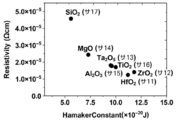
- FIG. 10 is a diagram showing the relationship between the Hamaker constant of the anchor metal diffusion control layer and the electrical resistivity of the silver film for Samples 11 to 17. It is a figure which shows the analysis result by the X-ray photoelectron spectroscopy about the sample 11 and the sample 17.
- a numerical range expressed using “to” means a range including numerical values described before and after “to” as a lower limit value and an upper limit value.
- an upper limit value or a lower limit value described in a numerical range may be replaced with an upper limit value or a lower limit value in another numerical range.
- the upper limit value or the lower limit value described in a certain numerical range may be replaced with the values shown in the examples.
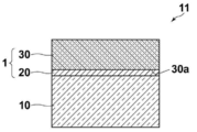
- FIG. 1 is a schematic cross-sectional view of an optical element 11 including an optical thin film 1 according to the first embodiment of the present invention.
- the optical thin film 1 of this embodiment includes a silver-containing metal layer 20 containing silver provided on one surface of a substrate 10 and a dielectric layer laminated in contact with the silver-containing metal layer 20.
- the dielectric layer 30 contains a metal oxide, and the first oxygen concentration of the first region including the first surface 30a in contact with the silver-containing metal layer 20 of the dielectric layer 30 has a metal concentration of It is smaller than the oxygen concentration of the stoichiometric composition of the oxide.
- silicon oxide, aluminum oxide, magnesium oxide, and the like having a sufficiently high light transmittance in the stoichiometric composition are suitable.
- a metal oxide having an oxygen concentration smaller than the oxygen concentration of the stoichiometric composition means that the ratio of oxygen to metal contained is smaller than the ratio of oxygen to metal in the stoichiometric composition of the metal oxide. means.
- the stoichiometric composition of silicon oxide is SiO 2 , but when silicon oxide is expressed as SiO n , if n is smaller than 2, the oxygen concentration is smaller than the stoichiometric composition.
- the first oxygen concentration in the first region 31 is preferably 0.95 times or less of the oxygen concentration of the stoichiometric composition.
- the first oxygen concentration is preferably 0.7 times or more, more preferably 0.8 times or more, and particularly preferably 0.9 times or more the oxygen concentration of the stoichiometric composition.
- the dielectric layer 30 is a single layer, and the composition of the metal oxide constituting the dielectric layer 30 is uniform over the entire area. That is, the entire dielectric layer 30 is the first region and is a layer having the first oxygen concentration. In the region in direct contact with the silver-containing metal layer 20, it is preferable that the first region having the first oxygen concentration is provided over 5 nm or more in the film thickness direction. Therefore, when the dielectric layer 30 is a single layer as in this embodiment, the dielectric layer 30 preferably has a thickness of 5 nm or more. Further, when the dielectric layer 30 is a single layer, it is preferably less than 150 nm, more preferably 100 nm or less, and further preferably 50 nm or less.
- the metal oxide used as the dielectric layer 30 has the maximum light transmittance in the stoichiometric composition, and the light transmittance decreases as the oxygen concentration decreases. Therefore, in order to ensure sufficient transparency, the following examination was performed. Here, the case where the metal oxide is silicon oxide was examined.
- k is the extinction coefficient of the substance
- d is the film thickness.
- silicon oxide represented by SiOn
- the extinction coefficient k 0 with respect to the wavelength of 400 nm, and in the case of SiO where the oxygen concentration is half of the oxygen concentration of the stoichiometric composition, with respect to the wavelength of 400 nm
- the extinction coefficient k 0.132.
- the extinction coefficient was quoted from “RefractiveIndex.INFO website, https://refractiveindex.info/” (reference date 2018-04-12).
- composition and film thickness range satisfy ( ⁇ 0.264X + 0.264) ⁇ d ⁇ 1.64, the transparency can be sufficiently secured, which is preferable.
- the silver in the silver-containing metal layer is oxidized and colored black and the refractive index may change.
- the present inventors have found that this is a problem that particularly occurs when an oxide layer is formed by a vapor phase method, and particularly when a film is formed by a sputtering method.
- a stoichiometric composition is preferred.
- excess oxygen is introduce
- silver is oxidized by this excessive oxygen.
- the metal oxide formed as the dielectric layer 30 has a lower oxygen concentration than the stoichiometric composition. That is, at the time of film formation, without introducing excessive oxygen into the film formation atmosphere, an amount of oxygen smaller than that required at the stoichiometric composition is introduced, or metal is oxidized in an atmosphere without introducing oxygen. A physical layer is formed. By forming such a film, the oxidation of silver in the silver-containing metal layer during the formation of the dielectric layer can be suppressed, and an optical thin film that maintains the original low refractive index and transparency when thin is obtained. Obtainable.
- the dielectric layer is mainly made of silicon oxide
- the same effect can be obtained even when the dielectric layer is an oxide of another metal such as aluminum oxide or magnesium oxide.
- the shape of the substrate 10 is not particularly limited, and is a transparent optical member (transparent substrate) mainly used in an optical device such as a flat plate, a concave lens, or a convex lens, and is configured by a combination of a curved surface and a flat surface having a positive or negative curvature. Substrates may also be used. A flexible film may be used as the substrate 10. As a material of the base material 10, glass or plastic can be used. In the present specification, “transparent” means that the internal transmittance is 10% or more with respect to light in the wavelength range of 400 nm to 800 nm, that is, visible light.
- the refractive index of the substrate 10 is not particularly limited, but is preferably 1.45 or more.
- the refractive index of the substrate 10 may be 1.61 or more, 1.74 or more, or even 1.84 or more.
- a high power lens such as a first lens of a combined lens of a camera may be used.
- the refractive index is shown as the refractive index for light having a wavelength of 550 nm.
- the silver-containing metal layer 20 is a metal layer in which 50 atomic% or more of the constituent elements is silver.
- silver is preferably 85 atomic% or more, and more preferably 90 atomic% or more.
- the silver-containing metal layer 20 includes palladium (Pd), copper (Cu), gold (Au), neodymium (Nd), samarium (Sm), bismuth (Bi), platinum (Pt), and tin (Sn).
- Aluminum (Al), zinc (Zn), magnesium (Mg), indium (In), gallium (Ga) and lead (Pb) may be contained.
- the silver-containing metal layer 20 preferably contains a metal having a standard electrode potential higher than that of silver.
- the silver-containing metal layer 20 has higher durability than a layer formed of only silver.
- Noble metals such as gold, platinum, and palladium are examples of metals having a higher standard electrode potential than silver.
- the real part of the refractive index of the silver containing metal layer 20 is 0.4 or less.
- an Ag—Nd—Cu alloy, an Ag—Pd—Cu alloy, an Ag—Bi—Nd alloy, or the like is preferable as a material for forming the silver-containing metal layer 20.
- the thickness of the silver-containing metal layer 20 is not limited, but is 20 nm or less, more preferably 10 nm or less, and more preferably 8 nm or less. The thinner, the greater the impact of silver being oxidized, and the higher the effect obtained by the technology of the present disclosure.
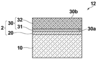
- FIG. 2 is a schematic cross-sectional view of an optical element 12 including an optical thin film 2 according to the second embodiment of the present invention.
- the same components as those in FIG. 1 are denoted by the same reference numerals, and detailed description thereof is omitted.
- the optical thin film 2 of this embodiment is similar to the optical thin film 1 of the said 1st Embodiment,
- the silver containing metal layer 20 containing the silver provided on one surface of the base material 10 is shown.
- the dielectric layer 30 contains a metal oxide, in addition to the first region 31 including the first surface 30a in contact with the silver-containing metal layer 20 of the dielectric layer 30.
- the first region 31 and the second region 32 are made of the same type of metal oxide, but have different oxygen concentrations.
- the first oxygen concentration in the first region 31 is smaller than the second oxygen concentration in the second region.
- the first oxygen concentration is smaller than the stoichiometric composition of the metal oxide.
- the second oxygen concentration in the second region 32 may be larger than the oxygen concentration in the first region 31 and not more than the stoichiometric composition of the metal oxide, but from the viewpoint of transparency, the second region
- the second oxygen concentration of 32 is preferably a stoichiometric composition of a metal oxide.
- the first region 31 is provided over 5 nm or more in the film thickness direction from the first surface 30 a. If the first region 31 is 2 nm or more, there is an effect of suppressing the oxidation of silver. However, if the first region 31 is provided over 5 nm or more, it is excessive in the film formation environment when forming the second region 32. Even when oxygen is introduced, the oxidation of silver can be sufficiently suppressed.
- the refractive index of the dielectric layer 30 is preferably 1.35 or more and 1.51 or less.
- the film thickness of the dielectric layer 30 is preferably about ⁇ / 4n where ⁇ is the target wavelength and n is the refractive index of the dielectric layer. Specifically, it is about 70 nm to 100 nm.
- the dielectric layer 30 is made of the same kind of metal oxide and is composed of a first region 31 and a second region 32 having different oxygen concentrations.
- regions having different oxygen concentrations may be included, and the oxygen concentration in the film thickness direction changes. You may do it.
- the oxygen concentration is present at the boundary between the first region 31 and the second region 32. There is a case where there is a region where the value gradually changes.
- the dielectric layer 30 may have a composition distribution in which the oxygen concentration gradually increases from the first surface 30a toward the second surface 30b and approaches the oxygen concentration of the stoichiometric composition. Good. Further, the oxygen concentration may change in a plurality of steps. Furthermore, a film region having a stoichiometric composition may be provided between the first region and the second region.
- the film formation of the first region 31 directly formed on the silver-containing metal layer 20 in the dielectric layer 30 is made more than the case where a film having a stoichiometric composition is formed. Since it can be performed in an atmosphere with a small amount of oxygen, the same effect as the optical thin film 1 of the first embodiment that suppresses oxidation of silver can be obtained.
- FIG. 3 is a schematic cross-sectional view of an optical element 13 including an optical thin film 3 according to the third embodiment of the present invention.
- the optical thin film 3 of the present embodiment has a relatively high refractive index between the silver-containing metal layer 20 and the substrate 10 in the optical thin film 2 of the second embodiment.
- An intermediate layer 40 including a high refractive index layer 41 and a low refractive index layer 42 having a relatively low refractive index is provided.
- the antireflection performance can be further improved by providing such an intermediate layer 40.
- the high refractive index layer 41 and the low refractive index layer 42 are each preferably provided with two or more layers, more preferably alternately stacked.
- the base 10 side may be the low-refractive index layer or the high-refractive index layer.
- the intermediate layer 40 is preferably composed of five or more layers.
- middle layer 40 is 20 layers or less from a viewpoint of film-forming cost and film-forming time.
- the refractive indexes of the high refractive index layer 41 and the low refractive index layer 42 are relatively determined and are not particularly limited.
- the refractive index of the high refractive index layer 41 is about 1.6 to 2.4.
- the refractive index of the low refractive index layer 42 is preferably about 1.3 to 1.8.
- the refractive index of the high refractive index layer 41 is more preferably 1.8 or more, and the refractive index of the low refractive index layer 42 is more preferably less than 1.7.
- the difference in refractive index between the adjacent high refractive index layer and low refractive index layer is preferably 0.4 or more, and more preferably 0.6 or more.
- the refractive index of the intermediate layer is a value measured by ellipsometry at a wavelength of 550 nm.
- the high refractive index layers 41 may not be the same material, and may not have the same refractive index. However, if the same refractive index is used as the same material, the material cost and the film forming cost are suppressed. From the viewpoint of Similarly, the low refractive index layers 42 do not have to be the same material and may not have the same refractive index. However, if the same refractive index is used as the same material, the material cost and the film forming cost are reduced. From the viewpoint of suppressing the above.
- the material constituting the high refractive index layer 41 and the low refractive index layer 42 is not particularly limited as long as it satisfies the refractive index condition. These are not limited to the stoichiometric composition as long as they are transparent to the wavelength of the light to be prevented from being reflected, and a non-stoichiometric composition can also be used. Introduction of impurities is also allowed for adjustment of optical properties such as refractive index, mechanical properties, and productivity.
- Examples of the material of the low refractive index layer 42 include silicon oxide, silicon oxynitride, gallium oxide, aluminum oxide, lanthanum oxide, lanthanum fluoride, magnesium fluoride, and mixtures thereof.
- silicon oxynitride is preferable.
- Examples of the material of the high refractive index layer 41 include niobium oxide, silicon niobium oxide, zirconium oxide, tantalum oxide, silicon nitride, titanium oxide, hafnium oxide, lanthanum titanate, and mixtures thereof.
- the compound constituting the low refractive index layer and the high refractive index layer is controlled to have a constituent element ratio deviating from the composition ratio of the stoichiometric ratio, or the refractive index is controlled by controlling the film formation density. It can be changed to some extent.
- the material constituting the low refractive index layer and the high refractive index layer is not limited to the above compound as long as the above refractive index condition is satisfied. Inevitable impurities may be included.
- each layer of the intermediate layer 40 it is preferable to use a physical vapor deposition method such as vacuum vapor deposition (particularly EB vapor deposition) or sputtering, or various chemical vapor deposition methods (CVD).
- a physical vapor deposition method such as vacuum vapor deposition (particularly EB vapor deposition) or sputtering, or various chemical vapor deposition methods (CVD).
- CVD chemical vapor deposition methods
- an ultra-thin silver film having a film thickness of 10 nm or less and further 6 nm or less as a smooth film. This is because when silver is formed by a vapor deposition method, silver is likely to aggregate and become granular.
- a metal other than silver can be added and alloyed to suppress aggregation, but an anchor metal layer that suppresses aggregation of silver is formed on the formation surface. It is also effective to prevent silver aggregation.
- the anchor metal layer bismuth (Bi), lead (Pb), tin (Sn), indium (In), magnesium (Mg), neodymium (Nd), zinc (Zn), Ga (gallium), germanium ( Ge) and silicon (Si), aluminum (Al), manganese (Mn), copper (Cu) and gold (Au).
- Ge, Au and Al are preferable.
- the anchor metal layer is preferably formed with a thickness of about 0.2 nm to 2 nm.
- the anchor metal diffuses in the silver film and its interface region in the manufacturing process, so that it is optically handled integrally, and the silver-containing metal layer
- the film thickness includes a region where the anchor metal is diffused.
- the film thickness of the silver-containing metal layer 20 can be determined by X-ray reflectivity measurement. Specifically, for example, a signal near the critical angle can be measured using RIGAKU RINTULTIMA III (CuK ⁇ line 40 kV 40 mA), and the obtained vibration component can be extracted and fitted.
- the metal which comprises an anchor metal layer is oxidized after film-forming of a silver film, and it makes it a metal oxide. Therefore, in the silver-containing metal layer, it is desirable that the content ratio of the anchor metal oxide is larger than the content ratio of the unoxidized anchor metal.
- the magnitude relationship between the content of the anchor metal oxide and the content of the non-oxidized anchor metal can be confirmed by the signal intensity ratio in the measurement by X-ray photoelectron spectroscopy (XPS).
- FIG. 4 shows the manufacturing process.
- the intermediate layer 40 is formed on the substrate 10 (Step 1).
- the anchor metal layer 21 and the silver film 22 are sequentially formed (Step 2).
- a layer made of a metal having a higher standard electrode potential may be formed between the anchor metal layer 21 and the silver film 22. .
- the film formation of the anchor metal layer 21 and the silver film 22 is performed in an atmosphere in which oxygen does not exist.
- the film thickness of the anchor metal layer 21 is preferably about 0.2 nm to 2.0 nm.
- middle layer 40, the anchor metal layer 21, and the silver film 22 is exposed to air
- the annealing temperature is preferably from 100 ° C. to 400 ° C.
- the annealing time is preferably from 1 minute to 2 hours.
- the anchor metal layer 21 is transformed into the anchor region 24, and a cap region 26 made of a metal oxide formed by oxidizing the anchor metal is formed on the surface side of the silver-containing metal layer 20 (Step 3). ).
- the anchor metal constituting the anchor metal layer 21 starts to move (diffuse) during the formation of the silver film 22 and moves to the surface side of the silver film 22.
- the anchor metal layer 21 is transformed into an anchor region 24, and a cap region 26 containing a metal oxide formed by oxidizing the anchor metal that has passed through the silver film 22 and moved to the surface of the laminate is formed.
- the silver-containing metal layer 20 includes a main body region 25, an anchor region 24, and a cap region 26.
- a dielectric layer 30 is formed on the silver-containing metal layer 20.
- the dielectric layer 30 may be formed by any film forming method performed in the presence of plasma.
- the dielectric layer 30 may be formed by a sputtering method or an ion assist method.
- a sputtering method or an ion assist method.
- the film formation step of the dielectric layer 30 first, the first region 31 of the dielectric layer 30 is formed on the silver-containing metal layer 20 (Step 4). At this time, the film is formed under a first condition in which the oxygen concentration in the formed film is lower than the condition for forming a film having a stoichiometric composition of a metal oxide.
- the condition for forming SiO 2 having a stoichiometric composition is that a SiO 2 target is used and oxygen at a predetermined flow rate is introduced into the chamber
- the first condition is that the SiO 2 target is It is sufficient to use a smaller amount of oxygen than the above predetermined flow rate or not introduce oxygen.
- oxygen defects are generated, and a film having an oxygen concentration lower than that of SiO 2 ⁇ x (x> 0) stoichiometry can be formed.
- the second region 32 is subsequently formed.
- the film is formed using the second condition in which the oxygen concentration in the film is higher than that of the film formed under the first condition (Step 5). For example, oxygen having a flow rate larger than that of oxygen introduced into the chamber under the first condition may be flowed.
- a sufficient flow rate of oxygen may be introduced.
- the optical thin film 3 of the third embodiment can be obtained.
- the first region formed directly on the silver-containing metal layer is formed under conditions that cause oxygen vacancies in the formed film, so that the silver in the silver-containing metal layer is oxidized during the film formation. This phenomenon can be effectively suppressed. Therefore, it is possible to produce an optical thin film having no coloration and no change in refractive index caused by the oxidation of silver in the silver-containing metal layer.
- an optical thin film is used as an antireflection film, transparency is ensured and a decrease in antireflection performance accompanying a change in refractive index can be suppressed.
- FIG. 5 is a schematic cross-sectional view of an optical element 14 including an optical thin film 4 according to the fourth embodiment of the present invention.
- the optical thin film 4 of this embodiment includes an anchor metal diffusion control layer 45 between the silver-containing metal layer 20 and the intermediate layer 40 in the optical thin film 3 of the third embodiment. Yes.
- the anchor metal diffusion control layer 45 is a layer provided for controlling the diffusion of the anchor metal.
- an ultra-thin silver-containing metal layer of 10 nm or less can be formed.
- the inventors have found that when the film thickness of the silver-containing metal layer 20 is 6 nm or less, the diffusion of the anchor metal constituting the anchor metal layer must be controlled when further ultrathinning is attempted. It was. Aggregation of silver can be suppressed by forming a silver film in a state where the anchor metal layer is not oxidized.
- the anchor metal diffuses, passes through the silver-containing metal layer, and moves to the cap region on the surface of the silver-containing metal layer. At this time, if all of the anchor metal moves to the cap region, the stability of the silver-containing metal layer 20 as a film is lowered, the flatness thereof is not maintained, and partial aggregation may occur.
- an anchor metal diffusion control layer 45 is provided as an underlayer of the anchor metal layer in order to control excessive diffusion of the anchor metal.
- the force to attract the anchor metal is important.
- the Hamaker constant which is an index of van der Waals force known as a force for attracting materials
- the present inventors have determined that the Hamaker constant is 7.3 ⁇ 10 ⁇ 20 J or more. It has been found that by providing the layer 45, the diffusion of the anchor metal can be suppressed, and an ultrathin silver-containing thin film layer of the order of several nm having high uniformity can be formed.
- the Hamaker constant can be obtained as follows based on the van Oss theory.
- ⁇ LW Liftshitz vdW
- ⁇ LW a Liftshitz vdW (van der Waals) term
- ⁇ ⁇ ⁇ donor term
- ⁇ + acceptor term
- the contact angles of the three liquids of water, diiodomethane, and ethylene glycol are measured, and the Lifshitz vdW term ( ⁇ LW ) in the surface energy of the thin film is calculated.
- D 0 0.165 nm by referring to the translation by
- the Hamaker constant is preferably 30.0 ⁇ 10 ⁇ 20 J or less.
- the anchor metal diffusion control layer 45 is not limited to any constituent material as long as the Hamaker constant satisfies 7.3 ⁇ 10 ⁇ 20 J or more, but is preferably transparent to visible light and sufficiently transparent. It is preferable to contain a metal oxide, a metal nitride, a metal oxynitride or a metal carbide in order to obtain properties. Specific examples of the constituent material include Si, Nb, Hf, Zr, Ta, Mg, Al, La, Y, or Ti oxides, nitrides, oxynitrides, carbides, and mixtures thereof. In general, a metal nitride has a higher Hamaker constant than an oxide of the same metal, so that the effect of suppressing the diffusion of the anchor metal is high.
- Hf oxide HfO 2
- the occupation ratio of the Hf oxide in the anchor metal diffusion control layer is more preferably 50 mol% or more, and it is particularly preferably composed of only HfO 2 (occupation ratio is 100 mol%).
- the inventors have confirmed that the homogeneity of the silver-containing metal layer is particularly high when HfO 2 is used (see Examples below).
- the thickness of the anchor metal diffusion control layer 45 is preferably 5 nm or more and 100 nm or less in order to improve the adhesion with the silver-containing metal layer 20.
- a material satisfying the above-described Hamaker constant may be used as the outermost layer of the intermediate layer 40.
- one layer of the intermediate layer 40 also serves as the anchor metal diffusion control layer 45.
- the intermediate layer 40 may be a low refractive index layer or a high refractive index layer as long as the conditions for the anchor metal diffusion control layer are satisfied.
- FIG. 6 is a schematic cross-sectional view illustrating a schematic configuration of the optical element 15 including the optical thin film 5 according to the fifth embodiment.
- the optical thin film 5 of the present embodiment is further provided with a fine uneven layer 50 on the surface of the dielectric layer 30 in the optical thin film 4 of the fourth embodiment.
- the fine uneven layer 50 is mainly composed of alumina hydrate.
- a main component means the component which occupies 80 mass% or more of the structural components of a fine uneven
- alumina hydrate refers to boehmite (expressed as Al 2 O 3 .H 2 O or AlOOH), which is alumina monohydrate, and Bayerlite (Al 2 O, which is alumina trihydrate). 3 ⁇ 3H 2 O or Al (OH) 3 .
- the fine concavo-convex layer 50 is transparent, and has a generally sawtooth cross section although the size of the convex portion (vertical angle size) and direction are various.
- corrugated layer 50 is the distance of the vertexes of the nearest convex part which separated the recessed part. The distance is less than or equal to the wavelength of the light to be prevented from being reflected. It is preferably on the order of several tens of nm to several hundreds of nm, 200 nm or less, and more preferably 150 nm or less.
- the fine uneven layer 50 is obtained by forming a thin film of a compound containing aluminum and immersing the thin film of the compound containing aluminum in hot water of 70 ° C. or higher for 1 minute or longer to perform hot water treatment.
- hot water treatment after forming an aluminum-containing film by vapor deposition such as vacuum deposition, plasma sputtering, electron cyclotron sputtering, or ion plating.
- the fine concavo-convex layer 50 made of hydrated alumina is provided on the outermost surface, it is necessary to perform hot water treatment as described above. Silver is oxidized by moisture. Therefore, when water enters from the fine uneven layer side to the silver-containing metal layer during the hot water treatment, there is a concern that the oxidation of silver is promoted by moisture and the silver-containing metal layer is damaged. However, since the dielectric layer functions as a protective film, moisture can be prevented from entering.
- the optical thin film 5 of the present embodiment is particularly suitable as an antireflection film and exhibits a very low reflectance with respect to visible light.
- the thickness of the silver-containing metal layer 20 including the anchor region and the cap region is preferably less than 3.5 nm. Further, the film thickness of the silver-containing metal layer 20 is preferably 0.5 nm or more, and more preferably 1.0 nm or more.
- the film thickness of the silver-containing metal layer is 3.5 nm or more, a very low reflectance as an antireflection film can be realized by providing a fine uneven layer on the surface.
- the effect of reducing the reflectance is remarkably enhanced by providing the fine uneven layer and making the film thickness of the silver-containing metal layer 20 less than 3.5 nm.
- optical thin film 1 of the first embodiment, the optical thin film 2 of the second embodiment, or the optical thin film 3 of the third embodiment may be an optical thin film having a structure with the fine uneven layer 50 on the outermost surface.
- Such an optical thin film is also an embodiment of the present invention.
- the configuration including the fine uneven layer of boehmite includes the fine uneven layer such as the optical thin films 1, 2, 3, and 4 of the first to fourth embodiments. Very low reflectivity is obtained compared to a configuration without it. On the other hand, the rub resistance is much higher in the case where the fine uneven layer is not provided. Therefore, when the optical thin film of the present invention is used as an antireflection film, a configuration with a fine uneven layer or a structure without a fine uneven layer may be used as appropriate depending on the application.
- optical thin film of the present disclosure may include other functional layers in addition to the above layers.
- the optical thin film of each of the above embodiments can be used for a transparent conductive film or an antireflection film. It is particularly suitable as an antireflection film and can be applied to the surface of various optical members.
- the optical thin film according to the first to fourth embodiments does not have a structure such as a concavo-convex structure or a porous structure on the surface, so that it has high mechanical strength and can be applied to a surface touched by a user's hand. It is. Since it can be applied to the surface of a lens having a high refractive index, it is suitable for the outermost surface of a known zoom lens described in, for example, Japanese Patent Application Laid-Open No. 2011-186417.
- the optical thin film 3 according to the third embodiment described above is an antireflection film (hereinafter referred to as an antireflection film 3), and the assembled lens includes an optical element in which the antireflection film is provided on the surface of the lens.
- FIGS. 7A, 7B, and 7C show configuration examples of a zoom lens that is an embodiment of the optical system of the present invention.
- 7A shows the arrangement of the optical system at the wide-angle end (shortest focal length state)
- FIG. 7B shows the arrangement of the optical system in the intermediate region (intermediate focal length state)
- FIG. 7C shows the telephoto end (longest length). This corresponds to the arrangement of the optical system in the focal length state.
- the zoom lens includes, in order from the object side along the optical axis Z1, a first lens group G1, a second lens group G2, a third lens group G3, a fourth lens group G4, and a fifth lens group G5. It has.
- the optical aperture stop S1 is preferably disposed near the object side of the third lens group G3 between the second lens group G2 and the third lens group G3.
- Each lens group G1 to G5 includes one or more lenses Lij.
- a symbol Lij indicates a jth lens that is assigned a symbol such that the most object side lens in the i-th lens group is the first lens and increases sequentially toward the imaging side.
- This zoom lens can be mounted not only on video cameras and digital still cameras, but also on portable information terminals.
- a member corresponding to the configuration of the photographing unit of the mounted camera is arranged on the image side of the zoom lens.
- an imaging element 100 such as a CCD (Charge-Coupled Device) or a CMOS (Complementary Metal-Oxide Semiconductor) is disposed on the imaging surface (imaging surface) of the zoom lens.
- Various optical members GC may be arranged between the final lens group (fifth lens group G5) and the image sensor 100 according to the configuration on the camera side where the lens is mounted.
- zooming is performed by moving at least the first lens group G1, the third lens group G3, and the fourth lens group G4 along the optical axis Z1 and changing the interval between the groups. ing. Further, the fourth lens group G4 may be moved at the time of focusing.
- the fifth lens group G5 is preferably always fixed during zooming and focusing.
- the aperture stop S1 moves with, for example, the third lens group G3. More specifically, as the magnification is changed from the wide-angle end to the intermediate range and further to the telephoto end, each lens unit and the aperture stop S1 are further changed from the state shown in FIG. 7A to the state shown in FIG. 7B, for example. It moves to the state of 7 (C) so that the locus
- the outermost surface of this zoom lens is provided with the antireflection film 3 on the outer surface (object side surface) of the lens L11 of the first lens group G1 and the lens L51 of the fifth lens group G5 which is the final lens group. That is, this is an embodiment of an optical element in which the lens L11 and the lens L51 are base materials and the antireflection film 3 is provided on the surface thereof. In this zoom lens, the antireflection film 3 may be similarly provided on other lens surfaces.
- the antireflection film 3 Since the antireflection film 3 has a high mechanical strength, it can be provided on the outermost surface of the zoom lens that may be touched by the user, and a zoom lens having a very high antireflection performance can be configured.
- a germanium film (film thickness 0.68 nm) is formed as an anchor metal layer on a SiO 2 glass substrate as a base material, and a gold film (film thickness 0.125 nm) is subsequently formed as a noble metal layer without exposure to the atmosphere.
- a silver film (film thickness 4 nm) was further formed.
- Each film was formed using a sputtering device (CFS-8EP) manufactured by Shibaura Mechatronics.
- the film formation conditions for each film were as follows. Below, room temperature is 20 degreeC or more and 30 degrees C or less.
- a dielectric layer was formed on the silver-containing metal layer.
- Each example and comparative example differ in the structure of the dielectric layer.
- a sputtering apparatus (CFS-8EP) manufactured by Shibaura Mechatronics was also used to form the dielectric layer.
- the dielectric layer was formed by radio frequency (RF) sputtering.
- -Dielectric layer deposition conditions A silicon oxide film was formed as the dielectric layer.
- the film was formed under different film formation conditions depending on the composition of each film.
- RF input power RF (W)
- the flow rate introduction amount
- Ar argon gas
- O 2 sccm
- Table 1 Each condition of the membrane pressure (Depo pressure (Pa)) is shown in Table 1 below.
- the composition of the target was SiO 2.
- the first region including the first surface in contact with the silver-containing metal layer of the dielectric layer was SiO 1.9
- the second region subsequently provided in the first region was SiO 2
- the second region is a region up to the second surface facing the first surface.
- the thicknesses of the first region and the second region in each example were as shown in Table 2.
- the stoichiometric composition of silicon oxide is SiO 2 .
- the second region has a stoichiometric composition
- the first region has a lower oxygen concentration than the stoichiometric composition.
- Example 5 In Example 1, the first region was SiO 1.8 , the thickness of the first region was 50 nm, and the thickness of the second region was 50 nm.
- the dielectric layer was made of SiO 1.9 over the entire area.
- the dielectric layer was made of SiO 2 having a stoichiometric composition over the entire area.
- the optical thin films of the examples and comparative examples were produced.
- ⁇ Measurement of composition of dielectric layer> The concentration distribution of the contained elements in the depth direction (film thickness direction) was measured. The concentration distribution was measured using X-ray photoelectron spectroscopy (XPS). Quantera SXM manufactured by PHI was used as a measuring device. As a result, it was confirmed that the composition and thickness were almost as designed.
- ⁇ Coloring evaluation> The coloration of the silver-containing metal layer after the dielectric layer was formed was evaluated visually.
- the evaluation criteria are as follows. The coloring is caused by the oxidation of silver, and when it is oxidized, black or brown coloring is observed. A: There is no coloring. B: Slight coloring can be visually recognized. C: Clear coloring is visually recognized.
- the refractive index of the silver-containing metal layer was determined by the following method. First, for each example and comparative example, the wavelength dependency of the double-sided transmittance and double-sided reflectance at wavelengths of 400 nm to 800 nm was measured with a spectrophotometer U-4000 (Hitachi High-Tech). And the refractive index of the silver containing metal layer which reproduces the measured value of the reflectance and transmittance obtained by this measurement was searched and derived with a self-made thin film calculation program.
- the thin film calculation program was created with reference to literature (basic theory of optical thin film, Mitsunobu Kohatayama, Optronics, 2011).
- the calculated refractive index value at a wavelength of 550 nm was evaluated according to the following criteria.
- the uniformity of the silver-containing metal layer and the permeability of the laminated film were evaluated.
- Comparative Example 1 since the coloring of silver was clear, the refractive index of the silver-containing metal layer was not obtained.
- Table 2 shows the production conditions and evaluation results of each example and comparative example.
- the composition of the dielectric layer formed in the region in contact with the silver-containing metal layer is such that the oxygen concentration is smaller than the stoichiometry, so that the silver is deposited during sputtering. It is clear that can be suppressed from being oxidized.
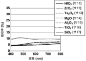
- an anchor metal diffusion control layer made of the material shown in Table 3 was formed on a glass substrate.
- a film was formed under the following conditions using a sputtering apparatus (CFS-8EP) manufactured by Shibaura Mechatronics.
- the following anchor metal layer and silver film were also formed using the same sputtering apparatus.
- an anchor metal layer made of Ge was successively formed without exposure to the atmosphere.
- the anchor metal diffusion control layer was 20 nm
- the anchor metal layer was 0.68 nm
- the silver film was 2 nm.
- the sample obtained as described above was evaluated for film uniformity and permeability.
- the electrical resistivity increases due to a partial increase in resistance in a discontinuous part of the silver-containing metal layer and a part where the film thickness changes, and is an index of film uniformity.
- the electrical resistivity decreases as the film uniformity (particularly flatness) increases, and increases as the film uniformity decreases.
- Table 3 summarizes the film configuration and measurement (evaluation) results for Samples 11 to 17 produced and evaluated by the above method.
- FIG. 10 is a graph showing the Ge element distribution in the depth direction from the surface in the stacking direction obtained by XPS toward the anchor metal diffusion control layer for Sample 11 and Sample 17. Drilling was performed by Ar + sputtering, and elemental analysis in the depth direction was performed.
- the horizontal axis 0 is the laminate surface position.
- the interface region between the silver-containing metal layer and the anchor metal diffusion control layer includes a region where the amount of Ge as an anchor metal increases, It can be seen that an anchor region is formed.
- SiO 2 is used for the anchor metal diffusion control layer
- Ge is reduced at the interface between the silver-containing metal layer and the anchor metal diffusion control layer, and the anchor metal layer formed on the anchor metal diffusion control layer It can be seen that most of Ge moves to the surface side of the silver-containing metal layer.
- HfO 2 having a high Hamaker constant can effectively suppress the diffusion of Ge. Since the diffusion of Ge is suppressed, the function as an anchor region that suppresses granulation of the silver-containing metal layer by the anchor metal is maintained, and it is assumed that the planarization of the silver-containing metal layer has been realized.
Landscapes
- Physics & Mathematics (AREA)
- General Physics & Mathematics (AREA)
- Optics & Photonics (AREA)
- Chemical & Material Sciences (AREA)
- Inorganic Chemistry (AREA)
- Nonlinear Science (AREA)
- Surface Treatment Of Optical Elements (AREA)
- Laminated Bodies (AREA)
- Physical Vapour Deposition (AREA)
Abstract
光透過率が高く、かつ高い耐久性を有する光学薄膜、光学薄膜を備えた光学素子および光学系、並びに光学薄膜の製造方法を提供する。 基材の一表面上に設けられた銀を含有する銀含有金属層と、銀含有金属層に接して積層された誘電体層とを備えた光学薄膜において誘電体層が、金属の酸化物を含有し、誘電体層の銀含有金属層と接する第1の面を含む第1の領域の第1の酸素濃度が、金属の酸化物のストイキオメトリ組成の酸素濃度よりも小さいものとする。
Description
本開示は、反射防止膜および透明導電膜等の光学薄膜、光学薄膜を備えた光学素子およびその光学素子を備えた光学系および光学薄膜の製造方法に関する。
従来、ガラスおよびプラスチックなどの透明基材においては、表面反射による透過光の損失を低減するために光入射面に反射防止膜が設けられる場合がある。そのような反射防止膜として、誘電体膜の積層体中に銀(Ag)を含有する銀含有金属層を含む反射防止膜が特開2013-238709号公報(以下において、特許文献1)、国際公開第2016-189848号(以下において、特許文献2)、特開2004-334012号公報(以下において、特許文献3)、特開平10-96801号公報(以下において、特許文献4)に提案されている。
特許文献1、2には、より低い反射率を実現するために、低屈折率層と高屈折率層とが交互に積層されてなる積層体と、空気への露出面を有する誘電体層との間に銀含有金属層を備えた構成が提案されている。銀含有金属層上に備えられる誘電体層の特に好ましい例としては、二酸化ケイ素(SiO2)が挙げられている。
一方で、銀含有金属層に直接SiO2層を備えた構成とすると、銀が酸化されてしまい、銀含有金属層が着色し透明性が低下するという問題、および屈折率が変化してしまい、反射防止効果が低減するという問題が生じる場合がある。特に銀含有金属層が薄くなればなるほど、この問題は顕著なものとなる。
特許文献3には、銀の酸化防止のため、銀膜の上層に窒化膜が設けられた構成が提案されている。
また、特許文献4では、金属層の酸化防止のために、金属層の上層に設けられるSiO2と金属層との間に窒化膜を設けることが開示されている。
しかしながら、特許文献3、4に記載のように、銀膜の酸化防止のため窒化膜を備える構成とした場合、窒化膜は酸化膜と比較して屈折率が高いために、銀の劣化を抑制可能なほどの厚みで備えられた場合、反射防止性能が低下する恐れがある。また、窒化膜を用いると光透明性が低下するという問題もある。
なお、薄膜化して透明性を向上させた銀含有金属層を有する光学薄膜は、上述のような反射防止膜としての利用に限るものではなく、透明導電膜などへの適用も考えられ、高いニーズがある。
本開示の技術が解決しようとする課題は、光透過率が高く、かつ高い耐久性を有する光学薄膜、光学薄膜を備えた光学素子および光学系、並びに光学薄膜の製造方法を提供することにある。
本開示の光学薄膜は、基材の一表面上に設けられた銀を含有する銀含有金属層と、
銀含有金属層に接して積層された誘電体層とを備え、
誘電体層が、金属の酸化物を含有し、誘電体層の銀含有金属層と接する第1の面を含む第1の領域の第1の酸素濃度が、金属の酸化物のストイキオメトリ組成の酸素濃度よりも小さい光学薄膜である。
銀含有金属層に接して積層された誘電体層とを備え、
誘電体層が、金属の酸化物を含有し、誘電体層の銀含有金属層と接する第1の面を含む第1の領域の第1の酸素濃度が、金属の酸化物のストイキオメトリ組成の酸素濃度よりも小さい光学薄膜である。
ここで銀含有金属層とは、銀を50原子%以上含む層を意味する。
本開示の光学薄膜においては、第1の酸素濃度がストイキオメトリ組成の酸素濃度の0.95倍以下であることが好ましい。
本開示の光学薄膜においては、誘電体層において、第1の領域が膜厚方向に5nm以上に亘って設けられていることが好ましい。
本開示の光学薄膜においては、誘電体層の第1の面に対向する第2の面を含む第2の領域の第2の酸素濃度よりも、第1の酸素濃度が小さいことが好ましい。
本開示の光学薄膜においては、金属の酸化物が、酸化シリコンであることが好ましい。
本開示の光学薄膜においては、誘電体層における第1の領域の第1の酸素濃度のストイキオメトリ組成の酸素濃度に対する比をX、第1の領域の厚みをdnm(ナノメートル)とした場合に、
(-0.264X+0.264)×d<1.64
X≦0.95、d≧5
を満たすことが好ましい。
(-0.264X+0.264)×d<1.64
X≦0.95、d≧5
を満たすことが好ましい。
本開示の光学薄膜においては、基材と銀含有金属層との間に、相対的に高い屈折率を有する高屈折率層と、相対的に低い屈折率を有する低屈折率層とを含む中間層を備えていてもよい。
ここで、「相対的に高い屈折率を有する」、「相対的に低い屈折率を有する」とは、高屈折率層と低屈折率層との相対的な関係をいうものであり、高屈折率層が低屈折率層よりも高い屈折率を有し、低屈折率層が高屈折率層よりも低い屈折率を有することを意味する。
ここで、「相対的に高い屈折率を有する」、「相対的に低い屈折率を有する」とは、高屈折率層と低屈折率層との相対的な関係をいうものであり、高屈折率層が低屈折率層よりも高い屈折率を有し、低屈折率層が高屈折率層よりも低い屈折率を有することを意味する。
本開示の光学薄膜においては、誘電体層の表面に、アルミナの水和物を主成分とする微細凹凸層をさらに備えていてもよい。
本開示の光学薄膜においては、上記微細凹凸層を備えた場合、銀含有金属層の膜厚が3.5nm未満であることが好ましい。
本開示の光学素子は、本開示の光学薄膜からなる反射防止膜を備えた光学素子である。
本開示の光学系は、本開示の光学素子の反射防止膜が設けられた面が最表面に配置されてなる組レンズを備えた光学系である。
ここで、最表面とは、複数のレンズからなる組レンズの端に配置されるレンズの一面であって、組レンズの端面となる面をいう。
ここで、最表面とは、複数のレンズからなる組レンズの端に配置されるレンズの一面であって、組レンズの端面となる面をいう。
本開示の光学薄膜の製造方法は、基材上に、銀を含有する銀含有金属層と、金属の酸化物を含有する誘電体層とを含む光学薄膜を製造する光学薄膜の製造方法であって、
基材上に設けられた銀含有金属層に接して誘電体層を、プラズマ存在下で実施される成膜法を用いて成膜する成膜工程を有し、
成膜工程において、誘電体層のうち銀含有金属層に接する面を含む第1の領域の成膜を、金属の酸化物のストイキオメトリ組成の膜を成膜する条件よりも、成膜された膜中の酸素濃度が小さくなる第1の条件で実施する光学薄膜の製造方法である。
基材上に設けられた銀含有金属層に接して誘電体層を、プラズマ存在下で実施される成膜法を用いて成膜する成膜工程を有し、
成膜工程において、誘電体層のうち銀含有金属層に接する面を含む第1の領域の成膜を、金属の酸化物のストイキオメトリ組成の膜を成膜する条件よりも、成膜された膜中の酸素濃度が小さくなる第1の条件で実施する光学薄膜の製造方法である。
本開示の光学薄膜の製造方法においては、成膜工程において、第1の条件を用いて第1の領域の成膜を行った後に、第1の条件よりも膜中の酸素濃度が大きくなる第2の条件を用いて成膜することが好ましい。
本開示の光学薄膜の製造方法においては、成膜法がスパッタリング法であり、
第1の条件として、金属の酸化物のストイキオメトリ組成の膜を成膜する場合にチャンバ内に導入する酸素量よりも、少ない量の酸素を導入すること、としてもよい。
第1の条件として、金属の酸化物のストイキオメトリ組成の膜を成膜する場合にチャンバ内に導入する酸素量よりも、少ない量の酸素を導入すること、としてもよい。
本開示の光学薄膜は、基材の一表面上に設けられた銀を含有する銀含有金属層と、銀含有金属層に接して積層された誘電体層とを備える。ここで、誘電体層が、金属の酸化物を含有し、誘電体層の銀含有金属層と接する第1の面を含む第1の領域の第1の酸素濃度が、金属の酸化物のストイキオメトリ組成の酸素濃度よりも小さい。係る構成により、本開示の光学薄膜は、光透過率が高く、かつ高い耐久性を有する。
以下、本発明の実施の形態を、図面を参照して説明する。
本明細書において、「~」を用いて表される数値範囲は、「~」の前後に記載される数値を下限値および上限値として含む範囲を意味する。本開示に段階的に記載されている数値範囲において、ある数値範囲で記載された上限値又は下限値は、他の段階的な記載の数値範囲の上限値又は下限値に置き換えてもよい。また、本開示に記載されている数値範囲において、ある数値範囲で記載された上限値又は下限値は、実施例に示されている値に置き換えてもよい。
本明細書において、「~」を用いて表される数値範囲は、「~」の前後に記載される数値を下限値および上限値として含む範囲を意味する。本開示に段階的に記載されている数値範囲において、ある数値範囲で記載された上限値又は下限値は、他の段階的な記載の数値範囲の上限値又は下限値に置き換えてもよい。また、本開示に記載されている数値範囲において、ある数値範囲で記載された上限値又は下限値は、実施例に示されている値に置き換えてもよい。
図1は、本発明の第1の実施形態に係る光学薄膜1を備えた光学素子11の断面模式図である。図1に示すように、本実施形態の光学薄膜1は、基材10の一表面上に設けられた銀を含有する銀含有金属層20と、銀含有金属層20に接して積層された誘電体層30とを備える。ここで、誘電体層30は、金属の酸化物を含有し、誘電体層30の銀含有金属層20と接する第1の面30aを含む第1の領域の第1の酸素濃度が、金属の酸化物のストイキオメトリ組成の酸素濃度よりも小さい。
誘電体層30を構成する金属の酸化物としては、ストイキオメトリ組成において光透過率が十分に高い、酸化シリコン、酸化アルミニウムおよび酸化マグネシウム等が好適である。ストイキオメトリ組成の酸素濃度よりも小さい酸素濃度の金属酸化物であるとは、金属酸化物のストイキオメトリ組成における酸素の金属に対する比率よりも含有されている酸素の金属に対する比率が小さいことを意味する。例えば、酸化シリコンのストイキオメトリ組成はSiO2であるが、酸化シリコンをSiOnで表記した場合に、nが2より小さければストイキオメトリ組成よりも酸素濃度が小さい、という。
なお、第1の領域31の第1の酸素濃度は、ストイキオメトリ組成の酸素濃度の0.95倍以下であることが好ましい。なお、透明性を担保するために、第1の酸素濃度は、ストイキオメトリ組成の酸素濃度の0.7倍以上が好ましく、0.8倍以上がさらに好ましく、0.9倍以上が特に好ましい。
なお、本実施形態の光学薄膜1においては、誘電体層30は単層であり、誘電体層30を構成する金属の酸化物の組成は全域に亘って均一なものとなっている。すなわち、誘電体層30は、全域が第1の領域であり、第1の酸素濃度の層である。銀含有金属層20に直接接する領域においては、第1の酸素濃度である第1の領域が膜厚方向に5nm以上に亘って設けられていることが好ましい。従って、本実施形態のように、誘電体層30が単層である場合には、誘電体層30は5nm以上の膜厚を有することが好ましい。また、誘電体層30が単層である場合には、150nm未満であることが好ましく、100nm以下であることがより好ましく、50nm以下がさらに好ましい。
誘電体層30として用いられる金属の酸化物は、ストイキオメトリ組成において光透過率が最大であり、酸素濃度が低下するほど光透過率が低下する。
そこで、十分な透明性を確保するために、以下の検討を行った。ここでは、金属の酸化物が酸化シリコンである場合について検討した。
そこで、十分な透明性を確保するために、以下の検討を行った。ここでは、金属の酸化物が酸化シリコンである場合について検討した。
物質の光透過率Tは、以下のベールの式によって表すことができる。
T=exp{(-4πk/λ)×d} (1)
ここで、kは物質の消衰係数、dは膜厚である。
λは光の波長であり、ここでλ=400nmに対して光透過率Tが95%以上である、すなわち、T≧0.95を満たせばよい、との基準を設定した。
酸化シリコンをSiOnで表した場合、ストイキオメトリであるSiO2との酸素濃度比Xは、X=n/2で示される。酸化シリコンのストイキオメトリ組成であるSiO2の場合、400nm波長に対し、消衰係数k=0であり、酸素濃度がストイキオメトリ組成の酸素濃度の半分であるSiOの場合、400nm波長に対し、消衰係数k=0.132である。なお、消衰係数は”RefractiveIndex.INFO website , https://refractiveindex.info/”(参照日2018-04-12)から引用した。
SiOnのn=2、すなわちX=1の場合のkが0、nが1、すなわちX=0.5の場合のkが0.132であることから、SiOnの消衰係数k=-0.264X+0.264と見積もることができる。
SiOnからなる膜の光透過率Tを0.95以下とするための条件は、
上記ベールの式から、k×d=(-0.264X+0.264)×d<1.64
である。
T=exp{(-4πk/λ)×d} (1)
ここで、kは物質の消衰係数、dは膜厚である。
λは光の波長であり、ここでλ=400nmに対して光透過率Tが95%以上である、すなわち、T≧0.95を満たせばよい、との基準を設定した。
酸化シリコンをSiOnで表した場合、ストイキオメトリであるSiO2との酸素濃度比Xは、X=n/2で示される。酸化シリコンのストイキオメトリ組成であるSiO2の場合、400nm波長に対し、消衰係数k=0であり、酸素濃度がストイキオメトリ組成の酸素濃度の半分であるSiOの場合、400nm波長に対し、消衰係数k=0.132である。なお、消衰係数は”RefractiveIndex.INFO website , https://refractiveindex.info/”(参照日2018-04-12)から引用した。
SiOnのn=2、すなわちX=1の場合のkが0、nが1、すなわちX=0.5の場合のkが0.132であることから、SiOnの消衰係数k=-0.264X+0.264と見積もることができる。
SiOnからなる膜の光透過率Tを0.95以下とするための条件は、
上記ベールの式から、k×d=(-0.264X+0.264)×d<1.64
である。
以上の通り、(-0.264X+0.264)×d<1.64を満たす組成と膜厚の範囲であれば、透明性は十分に担保でき、好ましい。
既述の通り、銀含有金属層上に酸化物層を積層する場合、銀含有金属層中の銀は酸化され、黒く着色が生じると共に、屈折率が変化してしまう場合があった。これは、特に気相法により酸化物層を成膜する際に生じ、特にはスパッタリング法により成膜する際に顕著に生じる問題であることを、本発明者らは見出した。金属の酸化物の透明性を高めるためには、ストイキオメトリ組成であることが好ましい。そして、金属を十分に酸化させるために、通常は過剰な酸素を成膜雰囲気中に導入する。しかし、この過剰な酸素により、銀が酸化されてしまうことを見出した。本実施形態の光学薄膜1においては、誘電体層30として成膜される金属の酸化物が、ストイキオメトリ組成よりも少ない酸素濃度である。すなわち、成膜時において、成膜雰囲気中に過剰な酸素を導入することなく、ストイキオメトリ組成時に要する酸素量よりも少ない量の酸素を導入する、もしくは酸素を導入しない雰囲気下で金属の酸化物層を成膜する。このような成膜により、誘電体層の成膜時における銀含有金属層の中の銀の酸化を抑制することができ、銀本来の低屈折率および薄膜時の透明性を維持した光学薄膜を得ることができる。
なお、ここでは主として、誘電体層が酸化シリコンからなる場合について説明したが、誘電体層が酸化アルミニウムあるいは酸化マグネシウムなどの他の金属の酸化物であっても同様の効果が得られる。
基材10の形状は特に限定なく、平板、凹レンズまたは凸レンズなど、主として光学装置において用いられる透明な光学部材(透明基材)であり、正または負の曲率を有する曲面と平面の組合せで構成された基材であってもよい。また、基材10として可撓性フィルムを用いてもよい。基材10の材料としては、ガラスあるいはプラスチックなどを用いることができる。本明細書において、「透明」とは、波長400nm~800nmの波長域の光、すなわち可視光に対して内部透過率が10%以上であることを意味する。
基材10の屈折率は、特に問わないが、1.45以上であることが好ましい。基材10の屈折率は1.61以上、1.74以上、さらには1.84以上のものであってもよい。基材10としては、例えば、カメラの組レンズの第1レンズなどの高パワーレンズであってもよい。なお、本明細書において、特に断らない限り屈折率は波長550nmの光に対する屈折率で示している。
銀含有金属層20は、構成元素の50原子%以上が銀である金属層である。銀含有金属層20において銀が85原子%以上であることが好ましく、90原子%以上であることがより好ましい。銀含有金属層20には、銀以外にパラジウム(Pd)、銅(Cu)、金(Au)、ネオジウム(Nd)、サマリウム(Sm)、ビスマス(Bi)、白金(Pt)、錫(Sn)、アルミニウム(Al)、亜鉛(Zn)、マグネシウム(Mg)、インジウム(In)、ガリウム(Ga)および鉛(Pb)のうちの少なくとも1種を含有していてもよい。銀含有金属層20は、標準電極電位が銀より高い金属を含有することが好ましい。標準電極電位が銀より高い金属を含むことにより、銀含有金属層20は、銀のみで形成される層と比較して高い耐久性を有するものとなる。貴金属である金、白金、パラジウムなどが、標準電極電位が銀より高い金属として挙げられる。
なお、光学薄膜1を反射防止膜として用いる場合には、銀含有金属層20の屈折率の実部が0.4以下であることが好ましい。
なお、光学薄膜1を反射防止膜として用いる場合には、銀含有金属層20の屈折率の実部が0.4以下であることが好ましい。
銀含有金属層20を形成するための材料としては、具体的には、例えば、Ag-Nd-Cu合金、Ag-Pd-Cu合金あるいはAg-Bi-Nd合金などが好適である。
銀含有金属層20の厚みは限定されないが、20nm以下、より好ましくは10nm以下であり、8nm以下がより好ましい。薄いほど、銀が酸化された場合の影響が大きいため、本開示の技術による高い効果が得られる。
図2は、本発明の第2の実施形態に係る光学薄膜2を備えた光学素子12の断面模式図である。以下において、図1と同等の構成要素には同一の符号を付し、詳細な説明は省略する。
図2に示すように、本実施形態の光学薄膜2は、上記第1の実施形態の光学薄膜1と同様に、基材10の一表面上に設けられた銀を含有する銀含有金属層20と、銀含有金属層20に接して積層された誘電体層30とを備える。本実施形態の光学薄膜2において、誘電体層30は、金属の酸化物を含有し、誘電体層30の銀含有金属層20と接する第1の面30aを含む第1の領域31に加えて、第1の面30aに対向する第2の面30bを含む第2の領域32を有する。第1の領域31と第2の領域32とは、同一種の金属の酸化物から構成されるが、酸素濃度が異なる。第1の領域31の第1の酸素濃度が第2の領域の第2の酸素濃度よりも小さい。なお、第1の酸素濃度は、金属の酸化物のストイキオメトリ組成よりも小さい。第2の領域32の第2の酸素濃度は、第1の領域31の酸素濃度よりも大きく、金属の酸化物のストイキオメトリ組成以下であればよいが、透明性の観点から第2の領域32の第2の酸素濃度は、金属の酸化物のストイキオメトリ組成であることが好ましい。
誘電体層30において、第1の領域31は、第1の面30aから膜厚方向に5nm以上に亘って設けられていることが好ましい。第1の領域31が2nm以上あれば、銀の酸化抑制の効果はあるが、5nm以上に亘って設けられていれば、第2の領域32の成膜時において、成膜環境下に過剰な酸素が導入された場合においても銀の酸化を十分に抑制することができる。
なお、光学薄膜2が反射防止膜である場合には、誘電体層30の屈折率は1.35以上1.51以下であることが好ましい。また、誘電体層30の膜厚は対象とする波長をλ、誘電体層の屈折率をnとしたとき、λ/4n程度であることが好ましい。具体的には70nm~100nm程度である。
本実施形態においては、誘電体層30が同一種の金属酸化物からなり、酸素濃度が異なる第1の領域31と第2の領域32とから構成されてなるものとしている。しかしながら、第1の領域31の酸素濃度が、ストイキオメトリ組成の酸素濃度よりも小さいという条件を満たせば、さらに異なる酸素濃度の領域を含んでいてもよいし、膜厚方向の酸素濃度が変化していてもよい。第1の領域31と第2の領域32を成膜雰囲気中に導入する酸素量を変化させることにより成膜する場合には、第1の領域31と第2の領域32との境界におい酸素濃度が徐々に変化する領域が存在する場合もある。
また、誘電体層30は、第1の面30aから第2の面30bに向かって、徐々に酸素濃度が増加してストイキオメトリ組成の酸素濃度に近づくような組成分布を有していてもよい。また、複数段階的に酸素濃度が変化してもよい。さらには、第1の領域と第2の領域との間にストイキオメトリ組成の膜領域を備えていてもよい。
また、誘電体層30は、第1の面30aから第2の面30bに向かって、徐々に酸素濃度が増加してストイキオメトリ組成の酸素濃度に近づくような組成分布を有していてもよい。また、複数段階的に酸素濃度が変化してもよい。さらには、第1の領域と第2の領域との間にストイキオメトリ組成の膜領域を備えていてもよい。
本実施形態の光学薄膜2についても、誘電体層30のうちの銀含有金属層20に直接形成される第1の領域31の成膜を、ストイキオメトリ組成の膜を成膜する場合よりも酸素量が少ない雰囲気下で行うことができるので、銀の酸化を抑制する上記第1の実施形態の光学薄膜1と同様の効果を得ることができる。
図3は、本発明の第3の実施形態に係る光学薄膜3を備えた光学素子13の断面模式図である。
図3に示すように、本実施形態の光学薄膜3は、上記第2の実施形態の光学薄膜2において、銀含有金属層20と基材10との間に、相対的に高い屈折率を有する高屈折率層41と、相対的に低い屈折率を有する低屈折率層42とを含む中間層40を備えている。
光学薄膜3が反射防止膜である場合、このような中間層40を備えることにより、反射防止性能をより向上させることができる。
中間層40において、高屈折率層41と低屈折率層42とは、それぞれ2層以上備えていることが好ましく、交互に積層されていることがより好ましい。高屈折率層41および低屈折率層42とのうち、最も基材10側は低屈折率層であっても高屈折率層であってもよい。より広い帯域において好ましい反射防止性能を得るためには、中間層40は、5層以上から構成されていることが好ましい。また、成膜コストおよび成膜時間の観点から中間層40は20層以下であることが好ましい。
高屈折率層41および低屈折率層42の屈折率は相対的に定められるものであるため、特に限定されないが、高屈折率層41の屈折率は1.6~2.4程度であるのが好ましく、低屈折率層42の屈折率は1.3~1.8程度であることが好ましい。高屈折率層41の屈折率は1.8以上であることがより好ましく、低屈折率層42の屈折率は1.7未満であることがより好ましい。また、隣接する高屈折率層と低屈折率層との屈折率差は0.4以上あることが好ましく、0.6以上であることがより好ましい。中間層の屈折率は、波長550nmでエリプソメトリーによって測定される値である。
高屈折率層41同士は、同一の材料でなくてもよく、また、同一の屈折率でなくても構わないが、同一材料として同一屈折率とすれば、材料コストおよび成膜コストなどを抑制する観点から好ましい。同様に、低屈折率層42同士は、同一の材料でなくてもよく、また、同一の屈折率でなくても構わないが、同一材料として同一屈折率とすれば、材料コストおよび成膜コストなどを抑制する観点から好ましい。
高屈折率層41および低屈折率層42を構成する材料は、屈折率の条件を満たすものであれば、特に限定されない。これらは、反射防止したい光の波長に対して透明であれば、ストイキオメトリ組成に限定されず、ノンストイキオメトリ組成も使用できる。屈折率などの光学特性、機械特性の調整および生産性を向上するなどのために不純物の導入も許容される。
低屈折率層42の材料としては、酸化シリコン素、酸窒化シリコン素、酸化ガリウム、酸化アルミニウム、酸化ランタン、弗化ランタン、および弗化マグネシウム、並びに、これらの混合物が挙げられる。特には酸窒化ケイ素が好ましい。
高屈折率層41の材料としては、酸化ニオブ、酸化シリコンニオブ、酸化ジルコニウム、酸化タンタル、窒化シリコン素、酸化チタン、酸化ハフニウム、およびチタン酸ランタン、並びに、これらの混合物が挙げられる。
低屈折率層および高屈折率層を構成するいずれの化合物も化学量論比の組成比からずれた構成元素比となるように制御する、あるいは、成膜密度を制御することにより、屈折率をある程度変化させることができる。なお、低屈折率層および高屈折率層を構成する材料としては、上述の屈折率の条件を満たすものであれば、上記化合物に限らない。また、不可避不純物が含まれていてもよい。
中間層40の各層の成膜には、真空蒸着(特にはEB蒸着)、スパッタなどの物理的気相成膜法あるいは各種の化学的気相成膜法(CVD)を用いることが好ましい。気相成膜によれば多様な屈折率、層厚の積層構造を容易に形成することができる。
光学薄膜の製造においては、膜厚を10nm以下、さらに6nm以下のような超薄膜の銀膜を平滑な膜として成膜するのは、非常に難しい。銀を気相成膜法により成膜する場合、銀は凝集しやすく粒状になるためである。既述のように、銀含有金属層として、銀以外の金属を添加し、合金化することにより凝集を抑制することができるが、形成面に銀の凝集を抑制するアンカー金属層を形成しておくことも銀の凝集を抑制するために効果的である。
アンカー金属層の材料としては、ビスマス(Bi)、鉛(Pb)、錫(Sn)、インジウム(In)、マグネシウム(Mg)、ネオジウム(Nd)、亜鉛(Zn)、Ga(ガリウム)、ゲルマニウム(Ge)およびシリコン(Si)、アルミニウム(Al)、マンガン(Mn)、銅(Cu)および金(Au)からなどが挙げられる。特には、Ge,AuおよびAlが好ましい。なお、アンカー金属層は0.2nmから2nm程度の膜厚で形成されることが好ましい。このようなアンカー金属層を銀膜の下地層として備えた場合は、製造過程において、アンカー金属は銀膜中およびその界面領域に拡散するため、光学的に一体的に扱われ、銀含有金属層の膜厚にはアンカー金属が拡散した領域が含まれる。
銀含有金属層20の膜厚は、X線反射率測定により求めることができる。具体的には、例えば、RIGAKU RINTULTIMAIII(CuKα線40kV40mA)を用いて、臨界角近傍の信号を測定し、得られる振動成分を抽出し、フィッティングして得ることができる。
なお、アンカー金属層を下地層として備える場合には、銀膜の成膜後においてアンカー金属層を構成する金属を酸化させて金属酸化物とすることが透明性向上の観点から好ましい。従って、銀含有金属層において、アンカー金属酸化物の含有割合が酸化されていないアンカー金属の含有割合よりも大きいことが望ましい。アンカー金属の酸化物の含有割合および酸化されていないアンカー金属の含有割合の大小関係は、X線光電子分光法(X-ray Photoelectron Spectroscopy :XPS)に測定における信号強度比で確認することができる。
ここで、本発明の光学薄膜の製造方法の実施形態として、上述の第3の実施形態の光学薄膜を製造する製造工程について説明する。図4は製造工程を示す図である。
まず、基材10上に、中間層40を成膜する(Step1)。アンカー金属層21および銀膜22を順次成膜する(Step2)。なお、銀含有金属層に銀よりも標準電極電位が高い金属を添加する際には、アンカー金属層21と銀膜22との間に標準電極電位が高い金属からなる層を成膜すればよい。
アンカー金属層21および銀膜22の成膜は酸素が存在しない雰囲気下で行う。アンカー金属層21の成膜膜厚は0.2nm~2.0nm程度とすることが好ましい。
その後、中間層40、アンカー金属層21および銀膜22の順に積層された基材10を大気中に曝露し、大気中にてアニール処理を行う。アニール温度は100℃以上400℃以下、アニール時間は1分以上2時間以下程度が好ましい。このアニール処理により、アンカー金属層21はアンカー領域24に変質し、銀含有金属層20の表面側にはアンカー金属が酸化されてなる金属酸化物から構成されるキャップ領域26が形成される(Step3)。アンカー金属層21を構成するアンカー金属は、銀膜22の成膜中において移動(拡散)し始め、銀膜22の表面側に移動する。そしてアニール処理後において、アンカー金属層21はアンカー領域24に変質し、銀膜22中を通過して積層体の表面に移動したアンカー金属が酸化されてなる金属酸化物を含むキャップ領域26が形成されている。
なお、銀含有金属層20は、本体領域25とアンカー領域24およびキャップ領域26から構成される。
なお、銀含有金属層20は、本体領域25とアンカー領域24およびキャップ領域26から構成される。
その後、銀含有金属層20上に誘電体層30を成膜する。誘電体層30の成膜は、プラズマ存在下で実施される成膜法であればよく、例えば、スパッタリング法もしくはイオンアシスト法などにより行う。ここでは、スパッタリング法により成膜する場合について説明する。
誘電体層30の成膜工程においては、まず、銀含有金属層20上に誘電体層30のうちの第1の領域31の成膜を行う(Step4)。このとき、金属の酸化物のストイキオメトリ組成の膜を成膜する条件よりも、成膜された膜中の酸素濃度が小さくなる第1の条件で成膜する。例えば、ストイキオメトリ組成であるSiO2を成膜する条件が、SiO2ターゲットを用い、所定流量の酸素をチャンバ内に導入するというものである場合、第1の条件としては、SiO2ターゲットを用い、上記の所定流量よりも少ない量の酸素を導入する、あるいは酸素を導入しないこと、とすればよい。このような第1の条件でスパッタを行うと、酸素欠陥が生じ、SiO2-x(x>0)ストイキオメトリの酸素濃度よりも少ない酸素濃度の膜を成膜することができる。
上記のようにして第1の領域31を成膜した後、引き続き、第2の領域32を成膜する。この場合、第1の条件よりで成膜した膜よりも膜中の酸素濃度が大きくなる第2の条件を用いて成膜する(Step5)。例えば、第1の条件でチャンバ内に導入される酸素の流量よりも大きい流量の酸素を流せばよい。第2の領域においてストイキオメトリ組成の膜を成膜する場合には、十分な流量の酸素を導入すればよい。
以上の方法により、第3の実施形態の光学薄膜3を得ることができる。
銀含有金属層に直接成膜される第1の領域の成膜を、成膜される膜中に酸素欠損が生じる条件で行うことにより、成膜時に銀含有金属層中の銀が酸化されるという現象を効果的に抑制することができる。従って、銀含有金属層における銀が酸化されることにより生じる、着色および屈折率の変化を有しない光学薄膜を製造することができる。
光学薄膜を反射防止膜として用いる場合には、透明性が担保され、また、屈折率変化に伴う反射防止性能の低下を抑制することができる。
光学薄膜を反射防止膜として用いる場合には、透明性が担保され、また、屈折率変化に伴う反射防止性能の低下を抑制することができる。
次に、本発明の光学薄膜の第4の実施形態について説明する。図5は、本発明の第4の実施形態に係る光学薄膜4を備えた光学素子14の断面模式図である。
図5に示すように、本実施形態の光学薄膜4は、上記第3の実施形態の光学薄膜3において、銀含有金属層20と中間層40との間にアンカー金属拡散制御層45を備えている。
アンカー金属拡散制御層45は、上記のアンカー金属の拡散を制御するために設けられる層である。上記第3の実施形態の光学薄膜およびその製造方法において説明したアンカー金属層を導入することで10nm以下の超薄膜の銀含有金属層の形成が可能になる。しかしながら、銀含有金属層20の膜厚が6nm以下において、さらなる超薄膜化を図る場合には、アンカー金属層を構成するアンカー金属の拡散を制御しなくてはならないことを本発明者らは見出した。アンカー金属層は酸化されていない状態で銀膜を形成することにより、銀の凝集を抑制することができる。既述の通り、アンカー金属層および銀膜を成膜した後にアニール処理されることにより、アンカー金属が拡散して銀含有金属層を通り抜けて銀含有金属層表面のキャップ領域に移動する。この際、アンカー金属の全てがキャップ領域に移動してしまうと、銀含有金属層20の膜としての安定性が低下し、その平坦性が保たれず、一部凝集等が生じる場合がある。
そこで、本実施形態の光学薄膜4においては、アンカー金属の過剰な拡散を制御するために、アンカー金属層の下地層として、アンカー金属拡散制御層45を備えている。アンカー金属拡散制御層45としては、アンカー金属を引きつける力が重要である。本発明者らは、物質同士を引き合う力として知られているファンデルワールス力の指標であるHamaker定数に着目し検討した結果、Hamaker定数が7.3×10⁻²⁰J以上のアンカー金属拡散制御層45を備えることにより、アンカー金属の拡散を抑制し、高い均一性を有する数nmのオーダーの超薄膜な銀含有薄膜層を形成できることを見出した。
Hamaker定数は、van Ossの理論に基づき、以下のようにして求めることができる。表面エネルギーγをγ=γLW+2(γ+γ-)1/2 としてLifshitz vdW(van der Waals)項(γLW)とドナー項(γ-)とアクセプター項(γ+)の3成分に分けて算出する。水、ジヨードメタンおよびエチレングリコールの3液の接触角を測定し、薄膜の表面エネルギーにおけるLifshitz vdW項(γLW)を算出する。そして、Hamaker定数A11を、A11=24πD0
2γLWより算出する。なお、分子間力と表面力(第3版)朝倉書店J.N.イスラエルアチヴィリ 著/大島広行 訳を参照してD0=0.165nmを採用(経験則より)する。
なお、既述の通り、ある程度のアンカー金属の拡散は、キャップ領域形成のために好ましく、Hamaker定数は30.0×10⁻²⁰J以下であることが好ましい。
アンカー金属拡散制御層45は、Hamaker定数が7.3×10-20J以上を満たすものであれば、構成材料に制限はないが、可視光に対して透明であることが好ましく、十分な透明性を得るために金属酸化物、金属窒化物、金属酸窒化物あるいは金属炭化物を含有することが好ましい。具体的な構成材料としては、Si、Nb、Hf、Zr、Ta、Mg、Al、La、Y、またはTiの酸化物、窒化物、酸窒化物あるいは炭化物、およびそれら混合物などが挙げられる。一般に、金属の窒化物は同一金属の酸化物よりもHamaker定数が大きいことから、アンカー金属の拡散を抑制する効果は高い。一方で、金属の酸化物は窒化物よりも透明性に優れる。より具体的には、MgO(A11=7.3×10⁻²⁰J)、Ta2O5(A11=9.5×10⁻²⁰J)、Al2O3(A11=9.6×10⁻²⁰J)、TiO2(A11=10×10-20J)、HfO2(A11=11.2×10⁻²⁰J)、ZrO2(A11=11.8×10⁻²⁰)、SiN(A11=9.5×10⁻²⁰J)およびNb2O5(A11=12×10-20J)等があげられる。かっこ内はHamaker定数A11である。中でも、Hf酸化物(HfO2)を含有することが好ましい。アンカー金属拡散制御層中におけるHf酸化物の占有割合は50mol%以上であることがより好ましく、HfO2のみで構成されている(占有割合100mol%である)ことが特に好ましい。HfO2を用いた場合の銀含有金属層の均一性が特に高いことを発明者らは確認している(後記実施例参照。)。
アンカー金属拡散制御層45の膜厚としては銀含有金属層20との密着性向上のために5nm以上100nm以下が好ましい。
なお、中間層40の最表層として、上記Hamaker定数を満たす材料を用いてもよい。この場合、中間層40の一層が、アンカー金属拡散制御層45を兼ねるものとなる。この場合、アンカー金属拡散制御層としての条件を満たせば、中間層40における低屈折率層であっても、高屈折率層であってもよい。
なお、中間層40の最表層として、上記Hamaker定数を満たす材料を用いてもよい。この場合、中間層40の一層が、アンカー金属拡散制御層45を兼ねるものとなる。この場合、アンカー金属拡散制御層としての条件を満たせば、中間層40における低屈折率層であっても、高屈折率層であってもよい。
以上のような銀含有金属層においてアンカー領域およびキャップ領域を備え、かつ、アンカー金属拡散制御層を備えることにより、平坦性と透明性を両立させた銀の超薄膜構造の実現が可能である。
次に、本発明の第5の実施形態に係るは光学薄膜について説明する。
図6は、第5の実施形態に係る光学薄膜5を備えた光学素子15の概略構成を示す断面模式図である。
図6は、第5の実施形態に係る光学薄膜5を備えた光学素子15の概略構成を示す断面模式図である。
図6に示すように、本実施形態の光学薄膜5は、上記第4の実施形態の光学薄膜4において、誘電体層30の表面にさらに微細凹凸層50を備えている。
微細凹凸層50は、アルミナの水和物を主成分とする。ここで、主成分とは、微細凹凸層の構成成分のうちの80質量%以上を占める成分をいう。ここでアルミナの水和物とは、アルミナ1水和物であるベーマイト(Al2O3・H2OあるいはAlOOHと表記される。)、およびアルミナ3水和物であるバイヤーライト(Al2O3・3H2OあるいはAl(OH)3と表記される。)などである。
微細凹凸層50は、アルミナの水和物を主成分とする。ここで、主成分とは、微細凹凸層の構成成分のうちの80質量%以上を占める成分をいう。ここでアルミナの水和物とは、アルミナ1水和物であるベーマイト(Al2O3・H2OあるいはAlOOHと表記される。)、およびアルミナ3水和物であるバイヤーライト(Al2O3・3H2OあるいはAl(OH)3と表記される。)などである。
微細凹凸層50は、透明であり、凸部の大きさ(頂角の大きさ)および向きは様々であるが、おおむね鋸歯状の断面を有している。この微細凹凸層50の凸部間の距離とは凹部を隔てた最隣接凸部の頂点同士の距離である。その距離は反射防止すべき光の波長以下である。数10nm~数100nmのオーダーであることが好ましく、200nm以下、さらには、150nm以下がより好ましい。
微細凹凸層50は、アルミニウムを含む化合物の薄膜を形成し、アルミニウムを含む化合物の薄膜を70℃以上の温水で1分以上浸漬させて温水処理することで得られる。特に、真空蒸着、プラズマスパッタ、電子サイクロトロンスパッタ、イオンプレーティングなどの気相成膜でアルミニウム含有膜を成膜後、温水処理することが好ましい。
最表面にアルミナの水和物からなる微細凹凸層50を備える場合、既述のように温水処理を行う必要がある。銀は水分によって酸化が促進される。したがって、温水処理の際に、微細凹凸層側から銀含有金属層まで水が浸入すると、水分によって銀の酸化が促進され、銀含有金属層がダメージを受けることが懸念される。しかしながら、誘電体層が保護膜として機能するので、水分の浸入を防止できる。
本実施形態の光学薄膜5は、反射防止膜として特に適し、可視光に対し非常に低い反射率を示す。反射防止性能をさらに高める観点から、アンカー領域およびキャップ領域を含む銀含有金属層20の膜厚は3.5nm未満であることが好ましい。また、銀含有金属層20の膜厚は0.5nm以上が好ましく、1.0nm以上がより好ましい。
上記銀含有金属層の膜厚が3.5nm以上であっても、表面に微細凹凸層を備えることにより、反射防止膜として非常に低い反射率を実現できる。しかし、微細凹凸層を備え、かつ、銀含有金属層20の膜厚を3.5nm未満とすることにより反射率の低減効果は格段に高まる。
なお、第1の実施形態の光学薄膜1、第2の実施形態の光学薄膜2、あるいは第3の実施形態の光学薄膜3の最表面に微細凹凸層50を備えた構成の光学薄膜としてもよく、このような構成の光学薄膜も本発明の一形態である。
第5の実施形態の光学薄膜5のように、ベーマイトの微細凹凸層を備えた構成では、第1から第4の実施形態の光学薄膜1,2,3および4のような微細凹凸層を備えない構成と比較して非常に低い反射率が得られる。一方で、擦り耐性は微細凹凸層を備えていないものの方が格段に高い。したがって、本発明の光学薄膜を反射防止膜として用いる場合には、用途に応じて適宜、微細凹凸層を備えた構成または微細凹凸層を備えない構成とすればよい。
なお、本開示の光学薄膜は、上記各層以外に、他の機能層を備えていてもよい。
上記各実施形態の光学薄膜は、透明導電膜あるいは反射防止膜などに用いることができる。反射防止膜として特に適し、種々の光学部材の表面に適用することができる。
なお、第1~第4の実施形態の光学薄膜は、表面に凹凸構造あるいはポーラス構造などの構造体を有していないので、機械的強度が高く、ユーザの手が触れる面への適用も可能である。高屈折率のレンズ表面への適用が可能であるため、例えば、特開2011-186417号公報等に記載の公知のズームレンズの最表面に好適である。
なお、第1~第4の実施形態の光学薄膜は、表面に凹凸構造あるいはポーラス構造などの構造体を有していないので、機械的強度が高く、ユーザの手が触れる面への適用も可能である。高屈折率のレンズ表面への適用が可能であるため、例えば、特開2011-186417号公報等に記載の公知のズームレンズの最表面に好適である。
上述の第3の実施形態の光学薄膜3が反射防止膜(以下において反射防止膜3とする。)であり、この反射防止膜がレンズの表面に設けられてなる光学素子を備えた組レンズからなる、本発明の光学系の実施形態を説明する。
図7(A),(B),(C)は、本発明の光学系の一実施形態であるズームレンズの構成例を示している。図7(A)は広角端(最短焦点距離状態)での光学系配置、図7(B)は中間域(中間焦点距離状態)での光学系配置、図7(C)は望遠端(最長焦点距離状態)での光学系配置に対応している。
図7(A),(B),(C)は、本発明の光学系の一実施形態であるズームレンズの構成例を示している。図7(A)は広角端(最短焦点距離状態)での光学系配置、図7(B)は中間域(中間焦点距離状態)での光学系配置、図7(C)は望遠端(最長焦点距離状態)での光学系配置に対応している。
このズームレンズは、光軸Z1に沿って物体側から順に、第1レンズ群G1と、第2レンズ群G2と、第3レンズ群G3と、第4レンズ群G4と、第5レンズ群G5とを備えている。光学的な開口絞りS1は、第2レンズ群G2と第3レンズ群G3との間で、第3レンズ群G3の物体側近傍に配設されていることが好ましい。各レンズ群G1~G5は1枚または複数のレンズLijを備えている。符合Lijは第iレンズ群中の最も物体側のレンズを1番目として結像側に向かうに従い順次増加するようにして符号を付したj番目のレンズを示す。
このズームレンズは、例えばビデオカメラ、およびデジタルスチルカメラ等の撮影機器のほか、情報携帯端末にも搭載可能である。このズームレンズの像側には、搭載されるカメラの撮影部の構成に応じた部材が配置される。例えば、このズームレンズの結像面(撮像面)には、CCD(Charge Coupled Device)あるいはCMOS(Complementary Metal Oxide Semiconductor)等の撮像素子100が配置される。最終レンズ群(第5レンズ群G5)と撮像素子100との間には、レンズを装着するカメラ側の構成に応じて、種々の光学部材GCが配置されていても良い。
このズームレンズは、少なくとも第1レンズ群G1、第3レンズ群G3、および第4レンズ群G4を光軸Z1に沿って移動させて、各群間隔を変化させることにより変倍を行うようになされている。また第4レンズ群G4を合焦時に移動させるようにしても良い。第5レンズ群G5は、変倍および合焦の際に常時固定であることが好ましい。開口絞りS1は、例えば第3レンズ群G3と共に移動するようになっている。より詳しくは、広角端から中間域へ、さらに望遠端へと変倍させるに従い、各レンズ群および開口絞りS1は、例えば図7(A)の状態から図7(B)の状態へ、さらに図7(C)の状態へと、図に実線で示した軌跡を描くように移動する。
このズームレンズの最表面は、第1レンズ群G1のレンズL11の外側面(物体側面)および最終レンズ群である第5レンズ群G5のレンズL51に反射防止膜3が備えられている。すなわちレンズL11およびレンズL51が基材であり、その表面に反射防止膜3が備えられてなる光学素子の実施形態である。なお、本ズームレンズにおいては、他のレンズ面にも同様に反射防止膜3を備えていてもよい。
反射防止膜3は機械的強度が大きいので、ユーザが触れる可能性のあるズームレンズの最表面に備えることができ、非常に反射防止性能の高いズームレンズを構成することができる。
以下、本発明の実施例および比較例の光学薄膜について説明する。
<実施例および比較例の作製方法>
基材としてのSiO2ガラス基板上にアンカー金属層としてゲルマニウム膜(膜厚0.68nm)を成膜し、大気に曝露することなく引き続き、貴金属層として金膜(膜厚0.125nm)を成膜し、さらに、銀膜(膜厚4nm)を成膜した。
基材としてのSiO2ガラス基板上にアンカー金属層としてゲルマニウム膜(膜厚0.68nm)を成膜し、大気に曝露することなく引き続き、貴金属層として金膜(膜厚0.125nm)を成膜し、さらに、銀膜(膜厚4nm)を成膜した。
各膜の成膜には、芝浦メカトロニクス社製スパッタ装置(CFS-8EP)を用いた。各膜の成膜条件は下記の通りとした。以下において、室温とは20℃以上30℃以下である。
-アンカー金属層成膜条件-
DC(直流)投入電力:20W、
Ar:20sccm、Depo圧(成膜圧力):0.45Pa
成膜温度:室温
DC(直流)投入電力:20W、
Ar:20sccm、Depo圧(成膜圧力):0.45Pa
成膜温度:室温
-金膜成膜条件-
DC投入電力:5W、
Ar:30sccm、Depo圧:0.8Pa
成膜温度:室温
DC投入電力:5W、
Ar:30sccm、Depo圧:0.8Pa
成膜温度:室温
-銀膜の成膜条件-
DC投入電力:80W、
Ar:15sccm、Depo圧:0.27Pa
成膜温度:室温
DC投入電力:80W、
Ar:15sccm、Depo圧:0.27Pa
成膜温度:室温
その後、大気中にて300℃、5分の条件でアニール処理を行った。このアニール処理により、銀、金およびゲルマニウムを含む銀含有金属層を形成した。
以上の工程は、実施例1~6および比較例1に共通とした。
以上の工程は、実施例1~6および比較例1に共通とした。
次に、この銀含有金属層上に誘電体層を成膜した。各実施例および比較例では、誘電体層の構造が異なる。誘電体層の成膜にも、芝浦メカトロニクス社製スパッタ装置(CFS-8EP)を用いた。なお、誘電体層の成膜は高周波(RF:radio Frequency)スパッタリングによって行った。
-誘電体層の成膜条件-
誘電体層として、酸化シリコンを成膜した。ここで、各膜の組成によって異なる成膜条件で成膜した。各組成を成膜する際のRF投入電力(RF(W))、成膜チャンバへのアルゴンガス(Ar(sccm))および酸素ガス(O2(sccm))のフロー量(導入量)および成膜圧力(Depo圧(Pa))の各条件を下記表1に示す。
ここでは、ターゲットの組成はSiO2とした。

誘電体層として、酸化シリコンを成膜した。ここで、各膜の組成によって異なる成膜条件で成膜した。各組成を成膜する際のRF投入電力(RF(W))、成膜チャンバへのアルゴンガス(Ar(sccm))および酸素ガス(O2(sccm))のフロー量(導入量)および成膜圧力(Depo圧(Pa))の各条件を下記表1に示す。
ここでは、ターゲットの組成はSiO2とした。
各実施例および比較例における誘電体層の構成は後記の表2にまとめて示す。
[実施例1~4]
誘電体層の銀含有金属層に接触する第1の面を含む第1の領域をSiO1.9、第1の領域に引き続き設けられる第2の領域をSiO2とした。ここでは、第2の領域は第1の面に対向する第2の面までの領域である。各例における第1の領域の厚みおよび第2の領域の厚みは表2に示す通りとした。酸化シリコンのストイキオメトリ組成はSiO2である。実施例1~4において、第2の領域はストイキオメトリ組成であり、第1の領域はストイキオメトリ組成よりも酸素濃度が小さい組成である。SiO1.9の酸素濃度のストイキオメトリの酸素濃度に対する比Xは、1.9/2=0.95である。
誘電体層の銀含有金属層に接触する第1の面を含む第1の領域をSiO1.9、第1の領域に引き続き設けられる第2の領域をSiO2とした。ここでは、第2の領域は第1の面に対向する第2の面までの領域である。各例における第1の領域の厚みおよび第2の領域の厚みは表2に示す通りとした。酸化シリコンのストイキオメトリ組成はSiO2である。実施例1~4において、第2の領域はストイキオメトリ組成であり、第1の領域はストイキオメトリ組成よりも酸素濃度が小さい組成である。SiO1.9の酸素濃度のストイキオメトリの酸素濃度に対する比Xは、1.9/2=0.95である。
[実施例5]
実施例1において、第1の領域をSiO1.8とし、第1の領域の厚みを50nm、第2の領域の厚みを50nmとした。
実施例1において、第1の領域をSiO1.8とし、第1の領域の厚みを50nm、第2の領域の厚みを50nmとした。
[実施例6]
誘電体層を全域に亘ってSiO1.9とした。
誘電体層を全域に亘ってSiO1.9とした。
[比較例1]
誘電体層を全域に亘ってストイキオメトリ組成であるSiO2とした。
誘電体層を全域に亘ってストイキオメトリ組成であるSiO2とした。
以上のようにして、各実施例および比較例の光学薄膜を作製した。
<光透過率の評価>
膜の組成の酸素濃度のストイキオメトリ組成の酸素濃度に対する比Xと、膜の厚みdとから、(-0.264×X+0.264)×dを求め、以下の基準で評価した。
A:(-0.264×X+0.264)×d<0.7
B:0.7≦(-0.264×X+0.264)×d<1.64
膜の組成の酸素濃度のストイキオメトリ組成の酸素濃度に対する比Xと、膜の厚みdとから、(-0.264×X+0.264)×dを求め、以下の基準で評価した。
A:(-0.264×X+0.264)×d<0.7
B:0.7≦(-0.264×X+0.264)×d<1.64
<誘電体層の組成測定>
深さ方向(膜厚方向)における含有元素の濃度分布を測定した。濃度分布の測定は、X線光電子分光法(X-ray Photoelectron Spectroscopy:XPS)を用いて行った。測定装置としてPHI社製Quantera SXMを用いた。結果、ほぼ設計通りの組成および厚みであることを確認した。
深さ方向(膜厚方向)における含有元素の濃度分布を測定した。濃度分布の測定は、X線光電子分光法(X-ray Photoelectron Spectroscopy:XPS)を用いて行った。測定装置としてPHI社製Quantera SXMを用いた。結果、ほぼ設計通りの組成および厚みであることを確認した。
<着色評価>
誘電体層が形成された後の銀含有金属層の着色を目視で評価した。評価基準は次の通りである。着色は銀の酸化によって生じ、酸化されると黒もしくは茶の着色が観察される。
A:着色がない。
B:やや着色が視認できる。
C:明らかな着色が視認される。
誘電体層が形成された後の銀含有金属層の着色を目視で評価した。評価基準は次の通りである。着色は銀の酸化によって生じ、酸化されると黒もしくは茶の着色が観察される。
A:着色がない。
B:やや着色が視認できる。
C:明らかな着色が視認される。
<銀含有金属層の屈折率評価>
銀含有金属層の屈折率は以下の方法により求めた。まず、各実施例および比較例について、波長400nm~800nmにおける両面透過率、両面反射率の波長依存性を分光光度計U-4000(日立ハイテック社)により測定した。そして、この測定で得られた反射率、透過率の測定値を再現する銀含有金属層の屈折率を、自作の薄膜計算プログラムにより探索して導出した。ここで、薄膜計算プログラムは文献(光学薄膜の基礎理論、小檜山 光信、オプトロニクス社、2011年)を参照して作成した。
銀含有金属層の屈折率は以下の方法により求めた。まず、各実施例および比較例について、波長400nm~800nmにおける両面透過率、両面反射率の波長依存性を分光光度計U-4000(日立ハイテック社)により測定した。そして、この測定で得られた反射率、透過率の測定値を再現する銀含有金属層の屈折率を、自作の薄膜計算プログラムにより探索して導出した。ここで、薄膜計算プログラムは文献(光学薄膜の基礎理論、小檜山 光信、オプトロニクス社、2011年)を参照して作成した。
算出した波長550nmでの屈折率の値を以下の基準で評価した。
A:0.3以下
B:0.3超、0.5以下
上記のようにして得られた実施例および比較例について、銀含有金属層の均一性および積層膜の透過性の評価を行った。なお、比較例1については、銀の着色が明らかであったため、銀含有金属層の屈折率は求めていない。
A:0.3以下
B:0.3超、0.5以下
上記のようにして得られた実施例および比較例について、銀含有金属層の均一性および積層膜の透過性の評価を行った。なお、比較例1については、銀の着色が明らかであったため、銀含有金属層の屈折率は求めていない。
表2に、各実施例および比較例の作製条件、および評価結果を併せて示す。
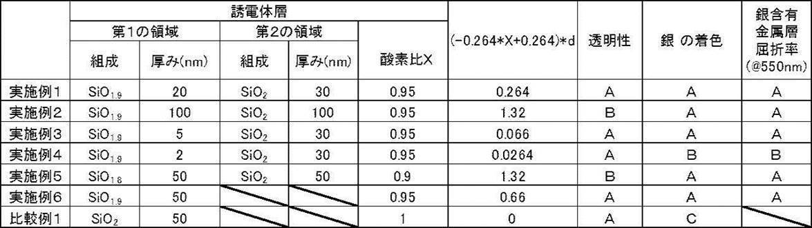
実施例1~6のように、銀含有金属層に接した領域に形成される誘電体層の組成をストイキオメトリよりも酸素濃度が小さくなる成膜条件ですることにより、スパッタ成膜時に銀が酸化されるのを抑制することができていることが明らかである。
次に、アンカー金属拡散制御層を備えたことによる効果を検証した結果を説明する。
ガラス基板上にアンカー金属拡散制御層、銀含有金属層としてアンカー領域、本体領域およびキャップ領域を備えたサンプルを作製し、その透明性および銀含有金属層の平坦性について評価した。
ガラス基板上にアンカー金属拡散制御層、銀含有金属層としてアンカー領域、本体領域およびキャップ領域を備えたサンプルを作製し、その透明性および銀含有金属層の平坦性について評価した。
<サンプルの作製方法>
まず、ガラス基板上に、表3に記載の材料からなるアンカー金属拡散制御層を成膜した。芝浦メカトロニクス社製スパッタ装置(CFS-8EP)を用いて下記条件にて成膜した。なお、下記アンカー金属層および銀膜も同一のスパッタ装置を用いて成膜した。
まず、ガラス基板上に、表3に記載の材料からなるアンカー金属拡散制御層を成膜した。芝浦メカトロニクス社製スパッタ装置(CFS-8EP)を用いて下記条件にて成膜した。なお、下記アンカー金属層および銀膜も同一のスパッタ装置を用いて成膜した。
-アンカー金属拡散制御層成膜条件-
RF(交流)投入電力=400W、
Ar:40sccm、O2:2.5sccm、Depo圧(成膜圧力):0.21Pa
成膜温度:室温
RF(交流)投入電力=400W、
Ar:40sccm、O2:2.5sccm、Depo圧(成膜圧力):0.21Pa
成膜温度:室温
アンカー金属拡散制御層の成膜後、大気に曝露することなく、引き続き、Geからなるアンカー金属層を順次成膜した。
-アンカー金属層成膜条件-
DC(直流)投入電力=20W、
Ar:20sccm、Depo圧(成膜圧力):0.45Pa
成膜温度:室温
DC(直流)投入電力=20W、
Ar:20sccm、Depo圧(成膜圧力):0.45Pa
成膜温度:室温
さらに、アンカー金属層の成膜後、大気に曝露することなく引き続き銀膜を成膜した。
-銀膜の成膜条件-
DC投入電力=80W、
Ar:15sccm、Depo圧:0.27Pa
成膜温度:室温
DC投入電力=80W、
Ar:15sccm、Depo圧:0.27Pa
成膜温度:室温
上記各層の成膜において、アンカー金属拡散制御層は20nm、アンカー金属層は0.68nm、銀膜は2nmの膜厚とした。
その後、大気中にて300℃、5minの条件でアニール処理を行った。
上記のようにして得られたサンプルについて、膜の均一性および透過性の評価を行った。
<平坦性の評価>
-可視光の吸収率による評価-
分光光度計により可視域である波長400nm~800nmにおける光の吸収率を測定した。具体的には、分光光度計(HITACHI U-4000)を用いて、波長400nm~800nmの範囲でスキャンスピード600nm/minで測定した。可視域におけるプラズモン吸収が生じると吸収率が上昇する。なお、吸収率は概ね10%以下であれば、実用上問題ないレベルである。図8は、各例についての測定結果であり、吸収率の波長依存性を示すグラフである。波長400nm~800nmの範囲において吸収率10%超を示したものにはプラズモン吸収が「有」、吸収率10%以下であったものにはプラズモン吸収が「無」として評価し、表3中に示した。
-可視光の吸収率による評価-
分光光度計により可視域である波長400nm~800nmにおける光の吸収率を測定した。具体的には、分光光度計(HITACHI U-4000)を用いて、波長400nm~800nmの範囲でスキャンスピード600nm/minで測定した。可視域におけるプラズモン吸収が生じると吸収率が上昇する。なお、吸収率は概ね10%以下であれば、実用上問題ないレベルである。図8は、各例についての測定結果であり、吸収率の波長依存性を示すグラフである。波長400nm~800nmの範囲において吸収率10%超を示したものにはプラズモン吸収が「有」、吸収率10%以下であったものにはプラズモン吸収が「無」として評価し、表3中に示した。
なお、銀は粒状化すると可視域におけるプラズモン吸収が生じることから、可視光の吸収率が上昇することは粒状化している部分が増加することを意味する。すなわち、吸収率が小さいほど、銀の粒状化が小さく、膜の平坦性が高いことを示す。また、可視光の吸収率の上昇は可視光の透過率の低下に繋がることから、吸収率の評価においてプラズモン吸収が「無」は、透明性が良好であることを意味する。
-電気抵抗率の測定-
各サンプルについて、四端子法による電気抵抗率(Ωcm)の測定を三菱化学製ロレスタGP、ESPプローブを用いて行った。測定結果を表2中に示した。
各サンプルについて、四端子法による電気抵抗率(Ωcm)の測定を三菱化学製ロレスタGP、ESPプローブを用いて行った。測定結果を表2中に示した。
電気抵抗率は、銀含有金属層に不連続な部分、および膜厚が変化する部分における部分的な抵抗上昇などにより上昇することから、膜の均一性の指標となる。電気抵抗率は、膜の均一性(特には、平坦性)が高いほど小さく、均一性が低いほど大きくなる。
<Hamaker定数の測定>
アンカー金属拡散制御層のHamaker定数は、既述の通り、van Ossの理論に基づいて求めた。
各例に用いられるアンカー金属拡散制御層を構成する材料を用い、別途ガラス基板上に20nmの厚みで成膜し、各材料による膜に関し、水、ジードメタン、エチレングリコールの3液の接触角をそれぞれKYOWA製Dropmasterにて液滴滴下法にて測定し、薄膜の表面エネルギーにおけるLifshitz vdW項(γLW)を求めた。そして、A11=24πD0 2γLWの関係式に基づいてHamaker定数A11を算出した。なお、ここでD0=0.165nmを採用した。
アンカー金属拡散制御層のHamaker定数は、既述の通り、van Ossの理論に基づいて求めた。
各例に用いられるアンカー金属拡散制御層を構成する材料を用い、別途ガラス基板上に20nmの厚みで成膜し、各材料による膜に関し、水、ジードメタン、エチレングリコールの3液の接触角をそれぞれKYOWA製Dropmasterにて液滴滴下法にて測定し、薄膜の表面エネルギーにおけるLifshitz vdW項(γLW)を求めた。そして、A11=24πD0 2γLWの関係式に基づいてHamaker定数A11を算出した。なお、ここでD0=0.165nmを採用した。
表3に上記方法によって作製し、評価したサンプル11~17についての膜構成および測定(評価)結果を纏めて示す。
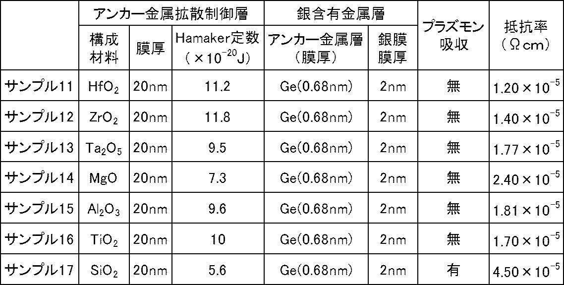
表3に示すように、アンカー金属拡散制御層のHamaker定数が7.3×10⁻²⁰J以上であるサンプル11~16については、サンプル17と比べて可視光のプラズモン吸収が抑制されており、かつ、電気抵抗率が低いという結果が得られた(図9参照)。すなわち、サンプル11~16は平坦性の高い銀膜を備えていると考えられる。
さらに、Hfを含むアンカー金属拡散制御層の効果について検証した結果を説明する。上記のようにして得られたアンカー金属拡散制御層としてHfO2を用いたサンプル11および、SiO2を用いたサンプル17の積層体について、深さ方向におけるGe量の分布を計測した。計測にはPHI社製Quantera SXMを用いたXPSを用いた。
図10は、サンプル11、サンプル17について、XPSにより取得された積層方向表面側からアンカー金属拡散制御層に向かう深さ方向におけるGe元素分布を示すグラフである。Ar+スパッタにより掘削し、深さ方向の元素分析を行った。図10において、横軸0が積層体表面位置である。
図10に示す通り、アンカー金属拡散制御層にHfO2を用いた場合、銀含有金属層とアンカー金属拡散制御層との界面領域にアンカー金属であるGeの量が増大する領域を備えており、アンカー領域が形成されていることがわかる。一方、アンカー金属拡散制御層にSiO2を用いた場合、銀含有金属層とアンカー金属拡散制御層との界面においてGeが少なくなっており、アンカー金属拡散制御層上に成膜されたアンカー金属層のGeの多くが銀含有金属層の表面側に移動していることが分かる。
本結果により、Hamaker定数の高いHfO2はGeの拡散を効果的に抑制することができることが確認できた。Geの拡散が抑制されているために、アンカー金属による銀含有金属層の粒状化を抑制するアンカー領域としての機能が維持されており、銀含有金属層の平坦化が実現できたと推察される。
2018年4月26日に出願された日本出願特願2018-085113号の開示はその全体が参照により本明細書に取り込まれる。
本明細書に記載された全ての文献、特許出願、および技術規格は、個々の文献、特許出願、および技術規格が参照により取り込まれることが具体的かつ個々に記された場合と同程度に、本明細書中に参照により取り込まれる。
本明細書に記載された全ての文献、特許出願、および技術規格は、個々の文献、特許出願、および技術規格が参照により取り込まれることが具体的かつ個々に記された場合と同程度に、本明細書中に参照により取り込まれる。
Claims (14)
- 基材の一表面上に設けられた銀を含有する銀含有金属層と、
該銀含有金属層に接して積層された誘電体層とを備え、
前記誘電体層が、金属の酸化物を含有し、該誘電体層の前記銀含有金属層と接する第1の面を含む第1の領域の第1の酸素濃度が、前記金属の酸化物のストイキオメトリ組成の酸素濃度よりも小さい光学薄膜。 - 前記第1の酸素濃度が、前記ストイキオメトリ組成の酸素濃度の0.95倍以下である請求項1に記載の光学薄膜。
- 前記誘電体層において、前記第1の領域が膜厚方向に5nm以上に亘って設けられている請求項1または2に記載の光学薄膜。
- 前記誘電体層の前記第1の面に対向する第2の面を含む第2の領域の第2の酸素濃度よりも、前記第1の酸素濃度が小さい請求項1から請求項3のいずれか1項に記載の光学薄膜。
- 前記金属の酸化物が、酸化シリコンである請求項1から請求項4のいずれか1項に記載の光学薄膜。
- 前記誘電体層における前記第1の領域の前記第1の酸素濃度の前記ストイキオメトリ組成の酸素濃度に対する比をX、前記第1の領域の厚みをdnmとした場合に、
(-0.264X+0.264)×d<1.64
X≦0.95、d≧5
を満たす請求項1から請求項5のいずれか1項に記載の光学薄膜。 - 前記基材と前記銀含有金属層との間に、相対的に高い屈折率を有する高屈折率層と、相対的に低い屈折率を有する低屈折率層とを含む中間層を備えている請求項1から請求項6のいずれか1項に記載の光学薄膜。
- 前記誘電体層の表面に、アルミナの水和物を主成分とする微細凹凸層を備えた請求項1から請求項7いずれか1項に記載の光学薄膜。
- 前記銀含有金属層の膜厚が3.5nm未満である請求項8に記載の光学薄膜。
- 請求項1から請求項9のいずれか1項に記載の光学薄膜からなる反射防止膜を備えた光学素子。
- 請求項10に記載の光学素子の前記反射防止膜が設けられた面が最表面に配置されてなる組レンズを備えた光学系。
- 基材上に、銀を含有する銀含有金属層と、金属の酸化物を含有する誘電体層とを含む光学薄膜を製造する光学薄膜の製造方法であって、
前記基材上に設けられた前記銀含有金属層に接して前記誘電体層を、プラズマ存在下で実施される成膜法を用いて成膜する成膜工程を有し、
該成膜工程において、前記誘電体層のうち前記銀含有金属層に接する面を含む第1の領域の成膜を、前記金属の酸化物のストイキオメトリ組成の膜を成膜する条件よりも、成膜された膜中の酸素濃度が小さくなる第1の条件で実施する光学薄膜の製造方法。 - 前記成膜工程において、前記第1の条件を用いて第1の領域の成膜を行った後に、該第1の条件よりも膜中の酸素濃度が大きくなる第2の条件を用いて成膜する請求項12に記載の光学薄膜の製造方法。
- 前記成膜法がスパッタリング法であり、
前記第1の条件が、前記金属の酸化物のストイキオメトリ組成の膜を成膜する場合にチャンバ内に導入する酸素量よりも、少ない量の酸素を導入することである請求項12または請求項13に記載の光学薄膜の製造方法。
Applications Claiming Priority (2)
| Application Number | Priority Date | Filing Date | Title |
|---|---|---|---|
| JP2018085113 | 2018-04-26 | ||
| JP2018-085113 | 2018-04-26 |
Publications (1)
| Publication Number | Publication Date |
|---|---|
| WO2019208366A1 true WO2019208366A1 (ja) | 2019-10-31 |
Family
ID=68294039
Family Applications (1)
| Application Number | Title | Priority Date | Filing Date |
|---|---|---|---|
| PCT/JP2019/016524 Ceased WO2019208366A1 (ja) | 2018-04-26 | 2019-04-17 | 光学薄膜、光学素子、光学系および光学薄膜の製造方法 |
Country Status (1)
| Country | Link |
|---|---|
| WO (1) | WO2019208366A1 (ja) |
Citations (3)
| Publication number | Priority date | Publication date | Assignee | Title |
|---|---|---|---|---|
| JP2010224350A (ja) * | 2009-03-25 | 2010-10-07 | Sumitomo Metal Mining Co Ltd | 吸収型多層膜ndフィルターとその製造方法 |
| WO2012127744A1 (ja) * | 2011-03-18 | 2012-09-27 | 富士フイルム株式会社 | 光学部材及びその製造方法 |
| WO2016189848A1 (ja) * | 2015-05-28 | 2016-12-01 | 富士フイルム株式会社 | 反射防止膜、光学素子および光学系 |
-
2019
- 2019-04-17 WO PCT/JP2019/016524 patent/WO2019208366A1/ja not_active Ceased
Patent Citations (3)
| Publication number | Priority date | Publication date | Assignee | Title |
|---|---|---|---|---|
| JP2010224350A (ja) * | 2009-03-25 | 2010-10-07 | Sumitomo Metal Mining Co Ltd | 吸収型多層膜ndフィルターとその製造方法 |
| WO2012127744A1 (ja) * | 2011-03-18 | 2012-09-27 | 富士フイルム株式会社 | 光学部材及びその製造方法 |
| WO2016189848A1 (ja) * | 2015-05-28 | 2016-12-01 | 富士フイルム株式会社 | 反射防止膜、光学素子および光学系 |
Similar Documents
| Publication | Publication Date | Title |
|---|---|---|
| CN111095037B (zh) | 防反射膜、光学元件及光学系统 | |
| JP6656389B2 (ja) | 反射防止膜、反射防止膜の製造方法、光学素子および光学系 | |
| US11747520B2 (en) | Optical thin film having metal layer containing silver and high standard electrode potential metal | |
| JP6817020B2 (ja) | 赤外線透過膜、光学膜、反射防止膜、光学部品、光学系及び撮像装置 | |
| JP6918208B2 (ja) | 反射防止膜および光学部材 | |
| US10641927B2 (en) | Optical thin film, optical element, optical system, and method for producing optical thin film | |
| JP6615407B2 (ja) | 透明光学膜の製造方法および透明多層膜の製造方法 | |
| JP6622381B2 (ja) | 光学膜、光学素子および光学系 | |
| JP6771572B2 (ja) | 反射防止膜、光学素子および光学系、並びに反射防止膜の製造方法 | |
| WO2019187417A1 (ja) | 反射防止膜、光学部材および反射防止膜の製造方法 | |
| JP7216471B2 (ja) | 車載レンズ用のプラスチックレンズ及びその製造方法 | |
| WO2019208366A1 (ja) | 光学薄膜、光学素子、光学系および光学薄膜の製造方法 | |
| WO2019064991A1 (ja) | 反射防止膜、光学素子および光学系 | |
| CN107102383B (zh) | 红外线透射膜、光学膜、防反射膜、光学部件、光学系统及摄像装置 | |
| JP7468624B2 (ja) | 光学部材 |
Legal Events
| Date | Code | Title | Description |
|---|---|---|---|
| 121 | Ep: the epo has been informed by wipo that ep was designated in this application |
Ref document number: 19793108 Country of ref document: EP Kind code of ref document: A1 |
|
| DPE2 | Request for preliminary examination filed before expiration of 19th month from priority date (pct application filed from 20040101) | ||
| NENP | Non-entry into the national phase |
Ref country code: DE |
|
| 122 | Ep: pct application non-entry in european phase |
Ref document number: 19793108 Country of ref document: EP Kind code of ref document: A1 |
|
| NENP | Non-entry into the national phase |
Ref country code: JP |