WO2019187761A1 - Tunable band-pass filter and method of controlling same - Google Patents
Tunable band-pass filter and method of controlling same Download PDFInfo
- Publication number
- WO2019187761A1 WO2019187761A1 PCT/JP2019/005726 JP2019005726W WO2019187761A1 WO 2019187761 A1 WO2019187761 A1 WO 2019187761A1 JP 2019005726 W JP2019005726 W JP 2019005726W WO 2019187761 A1 WO2019187761 A1 WO 2019187761A1
- Authority
- WO
- WIPO (PCT)
- Prior art keywords
- dielectric plate
- bandpass filter
- plate
- tunable bandpass
- waveguide
- Prior art date
Links
Images


Classifications
-
- H—ELECTRICITY
- H01—ELECTRIC ELEMENTS
- H01P—WAVEGUIDES; RESONATORS, LINES, OR OTHER DEVICES OF THE WAVEGUIDE TYPE
- H01P1/00—Auxiliary devices
- H01P1/20—Frequency-selective devices, e.g. filters
- H01P1/207—Hollow waveguide filters
-
- H—ELECTRICITY
- H01—ELECTRIC ELEMENTS
- H01P—WAVEGUIDES; RESONATORS, LINES, OR OTHER DEVICES OF THE WAVEGUIDE TYPE
- H01P1/00—Auxiliary devices
- H01P1/20—Frequency-selective devices, e.g. filters
- H01P1/201—Filters for transverse electromagnetic waves
- H01P1/203—Strip line filters
-
- H—ELECTRICITY
- H01—ELECTRIC ELEMENTS
- H01P—WAVEGUIDES; RESONATORS, LINES, OR OTHER DEVICES OF THE WAVEGUIDE TYPE
- H01P1/00—Auxiliary devices
- H01P1/20—Frequency-selective devices, e.g. filters
- H01P1/201—Filters for transverse electromagnetic waves
- H01P1/205—Comb or interdigital filters; Cascaded coaxial cavities
- H01P1/2053—Comb or interdigital filters; Cascaded coaxial cavities the coaxial cavity resonators being disposed parall to each other
-
- H—ELECTRICITY
- H01—ELECTRIC ELEMENTS
- H01P—WAVEGUIDES; RESONATORS, LINES, OR OTHER DEVICES OF THE WAVEGUIDE TYPE
- H01P7/00—Resonators of the waveguide type
- H01P7/06—Cavity resonators
Definitions
- the present disclosure relates to a tunable bandpass filter and a control method thereof.
- a band-pass filter In a communication apparatus that performs transmission and reception using the microwave and millimeter wave bands, a band-pass filter is used to pass only signals in a desired frequency band and remove unnecessary frequency components. Recently, there is an increasing demand for changing the pass band of the band pass filter from the outside.
- a tunable bandpass filter whose passband can be changed from the outside will be described.
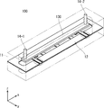
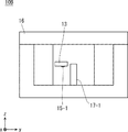
- FIGS. 1 and 2 are diagrams showing a configuration example of a tunable bandpass filter 100 according to the related art.
- FIG. 1 is a perspective view
- FIG. 2 is a bottom view.
- the tunable bandpass filter 100 according to the related technology includes a waveguide 11, a metal plate 12, a dielectric plate 130, and a support rod 14.
- the tunable bandpass filter 100 is a filter called a semi-coaxial filter or an evanescent mode filter.
- the waveguide 11 is a conductive rectangular waveguide.
- the waveguide 11 is divided into two members on a horizontal plane, and a plate-like metal plate 12 is sandwiched between the two members.
- the metal plate 12 is made of a plate-like conductor and extends in the longitudinal direction (x direction) of the waveguide 11.
- three resonance plates 121-1 to 121-3 and two input / output ports 122-1 to 122-2 are formed on the metal plate 12.
- resonance plates 121-1 to 121-3 may be simply referred to as “resonance plates 121”.
- input / output ports 122-1 to 122-2 may be simply referred to as “input / output ports 122”.
- the tunable bandpass filter 100 is a three-stage bandpass filter including three resonance plates 121-1 to 121-3.
- the number of stages of the tunable bandpass filter 100 is not limited to three but may be two or more.
- the resonance plates 121-1 to 121-3 have one end (plus y direction side) connected to the metal plate 12 and the other end (minus y direction side) an open end (that is, not in contact with other members). It is a plate-like resonator.
- the resonance plates 121-1 to 121-3 are housed in the waveguide 11, and are arranged in the longitudinal direction (x direction) of the waveguide 11 so that the side surfaces of the resonance plate 121 face each other.
- the resonance plates 121-1 to 121-3 operate so as to resonate at a resonance frequency determined by the shape, length (y direction), and the like.
- the input / output ports 122-1 to 122-2 are ports for inputting and outputting high-frequency signals.
- the input / output port 122-1 is connected to the resonance plate 121-1 by electromagnetic coupling, and the input / output port 122-2 is connected to the resonance plate 121-3 by electromagnetic coupling.
- One of the input / output ports 122-1 to 122-2 operates as an input port, and the other operates as an output port.
- a high-frequency signal is input to the input / output port 122-1 and within that passband of the tunable bandpass filter 100. Only the high-frequency signal is output from the input / output port 122-2.
- the dielectric plate 130 is made of a plate-like dielectric.
- the dielectric plate 130 extends in the longitudinal direction (x direction) of the waveguide 11, and the main surface (surface having the largest area) of the dielectric plate 130 faces the main surfaces of the resonance plates 121-1 to 121-3.
- the resonator plates 121-1 to 121-3 are arranged adjacent to each other.
- the support rods 14-1 and 14-2 are attached to both ends of the dielectric plate 130 in the x direction. Using a stepping motor (not shown) provided outside the tunable bandpass filter 100, the support rods 14-1 and 14-2 are moved in the vertical direction (that is, the z direction perpendicular to the main surface of the dielectric plate 130). ), The dielectric plate 130 can be moved in the vertical direction (z direction). Thus, the distance between the dielectric plate 130 and the resonance plates 121-1 to 121-3 is variable.
- the tunable bandpass filter 100 moves the dielectric plate 130 in the vertical direction (z direction) when changing the center frequency of the passband.
- the center frequency of the pass band increases as the dielectric plate 130 moves away from the resonance plates 121-1 to 121-3 (as the dielectric plate 130 moves upward (plus z direction)).
- the closer the dielectric plate 130 approaches the resonance plates 121-1 to 121-3 the more the dielectric plate 130 moves downward (minus z direction)
- the lower the center frequency of the pass band the center frequency of the pass band.
- the dielectric plate is arranged such that the main surface of the dielectric plate faces the main surface of the resonator, as in the tunable bandpass filter 100 according to the related art shown in FIGS.
- Patent Documents 1 and 2 disclose tunable bandpass filters that change the center frequency of the passband by moving a plate.
- the tunable bandpass filter disclosed in Patent Document 1 changes the center frequency of the passband by moving the dielectric plate in a direction perpendicular to and parallel to the main surface of the dielectric plate.
- the tunable bandpass filter disclosed in Patent Document 2 moves a tuning piece in a direction parallel to the main surface of a tuning piece corresponding to a dielectric plate, and a metal sheet formed on the tuning piece, and a metal plate
- the center frequency of the pass band is changed by changing the positional relationship with the window formed on the corresponding metal plate.
- the tunable bandpass filter 100 according to the related art shown in FIGS. 1 and 2 has a problem that the bandwidth of the passband varies greatly when the center frequency of the passband is changed. Hereinafter, this problem will be described in detail.
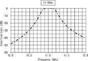
- FIGS. 3 to 5 are diagrams showing examples of passing waveforms of the tunable bandpass filter 100 according to the related art shown in FIGS. 1 and 2, in which the horizontal axis represents frequency [GHz] and the vertical axis represents pass. The loss [dB] is shown. 3, 4, and 5 are pass waveforms when the center frequencies of the passband are 10.6 [GHz], 11.0 [GHz], and 11.4 [GHz], respectively.
- FIG. 6 is a diagram in which the three passing waveforms shown in FIGS. 3 to 5 are superimposed so that the center frequencies match.
- FIG. 7 is a diagram illustrating an example of simulating the bandwidth characteristics of the tunable bandpass filter 100 according to the related technology illustrated in FIGS. 1 and 2 with respect to the center frequency of the passband.
- the horizontal axis represents the passband.
- the center frequency [GHz] and the vertical axis indicate the 3 dB bandwidth [MHz] of the pass band.
- the 3 dB bandwidth is a bandwidth at a point 3 dB lower than the peak of the passing waveform.
- 3 to 7 are designed under the condition that the number of filter stages is 3, the center frequency is 11.0 [GHz], the FRB (Full Ripple Band) is 200 [MHz], and the ripple is 0.01 [dB]. Simulates changing the center frequency.
- the tunable bandpass filter 100 As shown in FIGS. 3 to 7, the tunable bandpass filter 100 according to the related technique shown in FIGS. 1 and 2 has a center frequency of the passband of 10.6 [GHz] to 11.4 [GHz]. It can be seen that the bandwidth of the pass band fluctuates by 118 [MHz] when the frequency is changed to (change amount is 800 [MHz]).
- An object of the present disclosure is to solve the above-described problems and provide a tunable bandpass filter and a control method thereof that can suppress fluctuations in the bandwidth of the passband when the center frequency of the passband is changed. It is in.
- a tunable bandpass filter is A waveguide; A plurality of resonators housed in the waveguide and arranged in the longitudinal direction of the waveguide; A dielectric plate extending in the longitudinal direction of the waveguide and disposed adjacent to the plurality of resonators; A metal pattern for coupling adjustment formed at a position corresponding to the stage of the resonator in the dielectric plate, The distance between the dielectric plate and the resonator is variable.
- a method for controlling a tunable bandpass filter includes: In the waveguide, a plurality of resonators are arranged side by side in the longitudinal direction of the waveguide, A dielectric plate extending in the longitudinal direction of the waveguide is disposed adjacent to the plurality of resonators, Forming a metal pattern for coupling adjustment at a position corresponding to the stage of the resonator in the dielectric plate, The distance between the dielectric plate and the resonator is variable.
- FIG. 6 is a diagram in which three passing waveforms shown in FIGS.
- 3 to 5 are superimposed. It is a figure which shows the example which simulated the characteristic of the bandwidth with respect to the center frequency of a pass band of the tunable band pass filter which concerns on the related technique shown in FIG.1 and FIG.2. It is a figure which shows the example which simulated the characteristic of the coupling coefficient with respect to the center frequency of a pass band of the tunable band pass filter which concerns on the related technique shown in FIG.1 and FIG.2.
- 3 is a perspective view illustrating a configuration example of a tunable bandpass filter according to Embodiment 1.
- FIG. 3 is a bottom view showing a configuration example of a tunable bandpass filter according to Embodiment 1.
- FIG.9 and FIG.10 It is a bottom view which shows the structural example of the dielectric material board shown in FIG.9 and FIG.10. It is an enlarged side view which shows the structural example of the metal pattern vicinity of the tunable bandpass filter which concerns on Embodiment 1 shown in FIG.9 and FIG.10. It is an enlarged side view which shows the structural example of the metal pattern vicinity of the tunable bandpass filter which concerns on Embodiment 1 shown in FIG.9 and FIG.10. It is a bottom view which shows the structural example of the tunable bandpass filter used as the modification of the tunable bandpass filter which concerns on Embodiment 1 shown in FIG.9 and FIG.10.
- FIG. 20 is a view obtained by superimposing the three passage waveforms shown in FIGS. 17 to 19. It is a figure which shows the example which simulated the characteristic of the bandwidth with respect to the center frequency of a pass band of the tunable band pass filter which concerns on Embodiment 1 shown in FIG.9 and FIG.10.
- 6 is a perspective view showing a configuration example of a tunable bandpass filter according to Embodiment 2.
- FIG. 27 is a bottom view illustrating a configuration example of the dielectric plate illustrated in FIG. 26.
- FIG. 27 is a side view showing a configuration example of a tunable bandpass filter according to Embodiment 3 shown in FIG. 26.
- FIG. 27 is a side view showing a configuration example of a tunable bandpass filter according to Embodiment 3 shown in FIG. 26.
- FIG. 8 is a diagram illustrating an example of simulating the characteristics of the coupling coefficient with respect to the center frequency of the pass band of the tunable band pass filter 100 according to the related technique shown in FIGS. 1 and 2, and the horizontal axis represents the pass band.
- the center frequency [GHz] and the vertical axis indicate the coupling coefficient.
- the coupling coefficient indicates the coupling coefficient between the resonance plates 121
- the coupling coefficient k12 indicates the coupling coefficient between the resonance plates 121-1, 121-2
- the coupling coefficient k23 indicates the resonance plates 121-2, 121.
- the coupling coefficient between -3 is shown.
- the simulation conditions are the same as those in FIGS.
- the characteristics of the coupling coefficient with respect to the center frequency of the passband of the tunable bandpass filter 100 according to the related art shown in FIG. 1 and FIG. Indeed, the coupling coefficient is higher.
- the bandwidth characteristics with respect to the center frequency of the pass band are considered to rise to the right, that is, the higher the center frequency, the wider the bandwidth. .
- the characteristic of the coupling coefficient with respect to the center frequency of the pass band decreases downward along the dotted line shown in FIG. 8, that is, as the center frequency increases. It is necessary to make the characteristic that the coupling coefficient is low.
- the tunable bandpass filter according to each embodiment described below has a function of setting the characteristic of the coupling coefficient with respect to the center frequency of the passband to fall to the right, that is, the characteristic that the coupling coefficient decreases as the center frequency increases. Is provided.
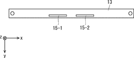
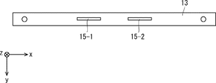
- FIGS. 9 and 10 are diagrams illustrating a configuration example of the tunable bandpass filter 10 according to the first embodiment, in which FIG. 9 is a perspective view and FIG. 10 is a bottom view.
- FIG. 11 is a bottom view illustrating a configuration example of the dielectric plate 13 illustrated in FIGS. 9 and 10.
- the tunable bandpass filter 10 according to the first embodiment is more dielectric than the tunable bandpass filter 100 according to the related art shown in FIGS.
- a dielectric plate 13 provided with metallic metal patterns 15-1 to 15-2 for adjusting coupling is provided.
- metal patterns 15-1 to 15-2 are referred to without any particular distinction, they may be simply referred to as “metal patterns 15”.
- the metal patterns 15-1 to 15-2 are formed at positions corresponding to the steps of the resonance plate 121 on the main surface opposite to the resonance plate 121 of the two main surfaces of the dielectric plate 13.
- the metal pattern 15-1 is formed at a position corresponding to the step between the resonance plates 121-1 and 121-2
- the metal pattern 15-2 is a position corresponding to the step between the resonance plates 121-2 and 121-3. Is formed.
- FIGS. 12 and 13 are enlarged side views showing a configuration example in the vicinity of the metal pattern 15 of the tunable bandpass filter 10 according to the first embodiment shown in FIGS. 9 and 10.
- FIG. 12 shows a state in which the dielectric plate 13 approaches the resonance plate 121 (metal plate 12) (a state in which the dielectric plate 13 has moved downward (minus z direction)).
- FIG. The state (state in which the dielectric plate 13 has moved upward (plus z direction)) away from the resonance plate 121 (metal plate 12) is shown.
- the tunable bandpass filter 10 according to the first embodiment is similar to the tunable bandpass filter 100 according to the related art, as the dielectric plate 13 approaches the resonance plate 121 (metal plate 12), the center of the passband is increased. The center frequency of the pass band increases as the frequency decreases and the dielectric plate 13 moves away from the resonance plate 121 (metal plate 12).
- the tunable bandpass filter 10 according to the first embodiment can not only change the center frequency of the passband by moving the dielectric plate 13 in the vertical direction (z direction),
- the coupling coefficient can also be changed.
- the characteristic of the coupling coefficient with respect to the center frequency of the pass band can be reduced to the right, that is, the characteristic that the coupling coefficient decreases as the center frequency increases.
- FIG. 14 is a bottom view illustrating a configuration example of a tunable bandpass filter 10A that is a modification of the tunable bandpass filter 10 according to the first embodiment illustrated in FIGS. 9 and 10.
- the tunable band-pass filter 10A shown in FIG. 14 is arranged such that the positions in the y direction of the metal patterns 15-1 to 15-2 are more open than the tunable band-pass filter 10 shown in FIGS. It is close to the end side (minus y direction side).
- FIG. 15 shows the tunable bandpass filter 10 according to the first embodiment shown in FIGS. 9 and 10 and the tunable bandpass filter 10A according to the modification of the first embodiment shown in FIG. It is a figure which shows the example which simulated the characteristic of the coupling coefficient with respect to the center frequency of a zone
- FIG. 15 also shows the characteristics of the tunable bandpass filter 100 according to the related technique shown in FIGS. 1 and 2 for comparison.
- the horizontal axis, the vertical axis, and simulation conditions are the same as those in FIG.
- the characteristics of the coupling coefficient of the tunable bandpass filters 10 and 10A according to the first embodiment with respect to the center frequency of the passband are lower right, that is, the higher the center frequency, It can be seen that the characteristic is low. Further, when comparing the characteristics of the tunable bandpass filters 10 and 10A, the inclination becomes steeper as the metal patterns 15-1 to 15-2 are brought closer to the open end side (minus y direction side) of the resonance plate 121. Recognize.
- FIG. 16 shows the characteristic of the coupling coefficient with respect to the center frequency of the pass band of the tunable band pass filter 10 according to the first embodiment shown in FIGS. 9 and 10, and the characteristic of the dotted line (bandwidth) shown in FIG. It is a figure which shows the example compared with the characteristic of the coupling coefficient required when making is constant.
- the characteristic of the coupling coefficient of the tunable bandpass filter 10 according to the first embodiment with respect to the center frequency of the passband does not completely match the characteristic of the dotted line shown in FIG. It can be seen that the amount of deviation between the two characteristics is greatly improved.
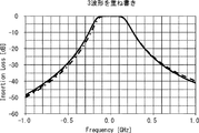
- FIG. 17 to FIG. 19 are diagrams showing examples of simulating the pass waveform of the tunable bandpass filter 10 according to the first embodiment shown in FIG. 9 and FIG. 17, 18 and 19 are pass waveforms when the center frequency of the pass band is 10.6 [GHz], 11.0 [GHz] and 11.4 [GHz], respectively.
- FIG. 20 is a diagram in which the three passing waveforms shown in FIGS. 17 to 19 are overlapped so that the center frequencies coincide with each other.
- FIG. 21 is a diagram illustrating an example of simulating the bandwidth characteristics of the tunable bandpass filter 10 according to the first embodiment illustrated in FIGS. 9 and 10 with respect to the center frequency of the passband.
- FIG. 21 also shows the characteristics of the tunable bandpass filter 100 according to the related technology shown in FIGS. 1 and 2 for comparison.
- the horizontal axis, the vertical axis, and the simulation conditions are the same as those in FIGS.
- the tunable bandpass filter 100 changes the center frequency of the passband from 10.6 [GHz] to 11.4 [GHz] (the amount of change is 800 [MHz]. ]), And the passband bandwidth fluctuated by 118 [MHz].
- the tunable bandpass filter 10 according to the first embodiment has a center frequency of the passband of 10.6 [GHz] to 11.4 [GHz]. Even if it is changed, it can be seen that the fluctuation of the bandwidth of the pass band is suppressed to 25 [MHz].
- the tunable bandpass filters 10 and 10A according to the first embodiment correspond to the steps between the resonance plates 121 in the dielectric plate 13 arranged so as to be adjacent to the plurality of resonance plates 121.
- a metal pattern 15 is formed at the position.
- the metal pattern 15 acts on the coupling coefficient between the resonance plates 121. Specifically, when the dielectric plate 13 is close to the resonance plate 121, the center frequency of the pass band is low, and the coupling between the resonance plates 121 is strengthened via the metal pattern 15. Becomes higher. Further, when the dielectric plate 13 is moved away from the resonance plate 121, the center frequency of the pass band becomes high, and the influence of the metal pattern 15 between the resonance plates 121 becomes weak, so that the coupling coefficient becomes low.
- the characteristics of the coupling coefficient of the tunable bandpass filters 10 and 10A according to the first embodiment with respect to the center frequency of the passband are lower right, that is, the characteristic that the coupling coefficient is lower as the center frequency is higher. Become. Therefore, the tunable bandpass filters 10 and 10A according to the first embodiment can suppress fluctuations in the bandwidth of the passband when the center frequency of the passband is changed.
- the position of the metal pattern 15 in the length direction (y direction) of the resonance plate 121, the length of the metal pattern 15 (x direction), the shape of the metal pattern 15 and the like are shown in FIGS. It is not limited to what was shown in FIG.
- the length (x direction) of the metal pattern 15 may be shorter than the length shown in FIGS.
- the shape of the metal pattern 15 may be, for example, a rectangular shape. good.
- the position of the metal pattern 15 in the length direction (y direction) of the resonance plate 121 is not particularly limited, but from one end connected to the metal plate 12 of the resonance plate 121 to the open end. The position between the ends is preferred.
- the metal pattern 15 is formed on the main surface of the dielectric plate 13 facing the resonance plate 121, but the present invention is not limited to this.
- the metal pattern 15 may be formed on the main surface of the dielectric plate 13 opposite to the main surface facing the resonance plate 121.
- the metal pattern 15 has a strong influence on the coupling coefficient because the resonance plate 121 of the dielectric plate 13. It is the direction of the main surface opposite to. Therefore, the metal pattern 15 is preferably formed on the main surface of the dielectric plate 13 that faces the resonance plate 121.
- the position of the metal pattern 15 in the y direction, the length of the metal pattern 15 (x direction), the shape of the metal pattern 15, the main surface of the dielectric plate 13 forming the metal pattern 15, etc. are changed,
- the characteristic of the coupling coefficient with respect to the center frequency changes such as a change in slope. Therefore, the position of the metal pattern 15 in the y direction, the length of the metal pattern 15 (x direction), the shape of the metal pattern 15, the main surface of the dielectric plate 13 forming the metal pattern 15, etc. What is necessary is just to determine suitably according to a width
- the dielectric plate 13 is disposed so that the main surface of the dielectric plate 13 faces the main surface of the resonance plate 121, and the dielectric plate 13 is perpendicular to the main surface of the dielectric plate 13. It was an example of moving in the direction.
- the second embodiment is an example in which the moving direction of the dielectric plate 13 is different from the first embodiment.
- FIG. 22 is a perspective view showing a configuration example of the tunable bandpass filter 10B according to the second embodiment.
- FIG. 23 is a bottom view showing a configuration example of the dielectric plate 13 shown in FIG.
- the tunable bandpass filter 10 according to Embodiment 1 shown in FIGS. 9 and 10 plate-like resonance plates 121-1 to 121-3 are formed on the metal plate 12 sandwiched between the waveguides 11. It was a configuration.
- the tunable bandpass filter 10B according to the second embodiment includes rod-shaped resonance bars 17-1 to 17-3 inside the waveguide 16. Is provided.
- the resonance bars 17-1 to 17-3 are referred to without particular distinction, they may be simply referred to as “resonance bars 17”.
- One end (minus z direction side) of the resonance rods 17-1 to 17-3 is connected to the lower surface of the waveguide 16, and the other end (plus z direction side) is an open end (that is, is not in contact with other members).
- This is a rod-shaped resonator.
- the resonance bars 17-1 to 17-3 are housed in the waveguide 16 and are arranged in the longitudinal direction (x direction) of the waveguide 16.
- the resonance bars 17-1 to 17-3 operate so as to resonate at a resonance frequency determined by the shape, length (z direction), and the like.
- the dielectric plate 13 extends in the longitudinal direction (x direction) of the waveguide 16, and the resonance bars 17-1 to 17-1 are arranged so that the side surfaces of the dielectric plate 13 face the side surfaces of the resonance bars 17-1 to 17-3. Arranged adjacent to 17-3.
- the support rods 14-1 and 14-2 at both ends in the x direction of the dielectric plate 13 are displaced in the vertical direction (that is, the z direction perpendicular to the main surface of the dielectric plate 13) using a stepping motor (not shown). By doing so, the dielectric plate 13 moves in the vertical direction (z direction).
- the metal patterns 15-1 to 15-2 are formed at positions corresponding to the steps of the resonance rod 17 on the lower main surface of the two main surfaces of the dielectric plate 13.
- the metal pattern 15-1 is formed at a position corresponding to the stage between the resonance bars 17-1 and 17-2
- the metal pattern 15-2 is a position corresponding to the stage between the resonance bars 17-2 and 17-3. Is formed.
- FIG. 24 and 25 are side views showing a configuration example of the tunable bandpass filter 10B according to the second embodiment shown in FIG. 24 shows a state in which the dielectric plate 13 approaches the open end of the resonance bar 17 (a state in which the dielectric plate 13 has moved upward (plus z direction)), and FIG. 25 shows a state in which the dielectric plate 13 is in the resonance bar. 17 shows a state in which the dielectric plate 13 is moved downward (minus z direction) away from the open end of 17.
- the center frequency of the passband decreases as the dielectric plate 13 approaches the open end of the resonance bar 17, and the dielectric plate 13 The further away from the open end, the higher the center frequency of the passband.
- the characteristic of the coupling coefficient with respect to the center frequency of the passband decreases, that is, as the center frequency increases.
- the coupling coefficient can be reduced.
- the position of the metal pattern 15 in the y direction, the length of the metal pattern 15 (x direction), the shape of the metal pattern 15, and the metal pattern 15 are formed.
- the main surface and the like of the dielectric plate 13 are not limited to those shown in FIGS.
- the first embodiment is an example applied to a semi-coaxial filter or an evanescent mode filter.
- the third embodiment is an example applied to a TE (Transverse Electric) mode filter.
- FIG. 26 is a perspective view showing a configuration example of a tunable bandpass filter 10C according to the third embodiment.
- FIG. 27 is a bottom view showing a configuration example of the dielectric plate 13 shown in FIG.
- the tunable bandpass filter 10C according to the third embodiment is compared with the tunable bandpass filter 10 according to the first embodiment shown in FIGS. The difference is that a ladder-like metal plate 18 is provided instead of the metal plate 12.
- the metal plate 18 is made of a plate-like conductor and extends in the longitudinal direction (x direction) of the waveguide 11.
- the metal plate 18 has a ladder shape, and cavities 181-1 to 181-3 where no metal is present serve as a resonator.
- cavities 181-1 to 181-3 may be simply referred to as “cavity 181”.
- the dielectric plate 13 extends in the longitudinal direction (x direction) of the waveguide 16 so that the main surface of the dielectric plate 13 faces the main surface of the cavities 181-1 to 181-3 (metal plate 18).
- the cavity portions 181-1 to 181-3 are arranged adjacent to each other.
- the support rods 14-1 and 14-2 at both ends in the x direction of the dielectric plate 13 are displaced in the vertical direction (that is, the z direction perpendicular to the main surface of the dielectric plate 13) using a stepping motor (not shown). By doing so, the dielectric plate 13 moves in the vertical direction (z direction).
- the metal patterns 15-1 to 15-2 are formed on the lower principal surface of the two principal surfaces of the dielectric plate 13 at positions corresponding to the steps of the cavity 181.
- the metal pattern 15-1 is formed at a position corresponding to the space between the cavities 181-1 and 181-2
- the metal pattern 15-2 is a position corresponding to the space between the cavities 181-2 and 181-3. Is formed.
- FIG. 28 and 29 are side views showing a configuration example of the tunable bandpass filter 10C according to the third embodiment shown in FIG.
- FIG. 28 shows a state in which the dielectric plate 13 approaches the cavity 181 (metal plate 18) (the state in which the dielectric plate 13 has moved downward (minus z direction)), and FIG. The state (dielectric plate 13) has moved upward (plus z direction) away from the cavity 181 (metal plate 18).
- the characteristic of the coupling coefficient with respect to the center frequency of the passband decreases downward, that is, as the center frequency increases, as in the first embodiment.
- the coupling coefficient can be reduced.
- the position of the metal pattern 15 in the y direction, the length of the metal pattern 15 (x direction), the shape of the metal pattern 15, and the metal pattern 15 are formed.
- the main surface and the like of the dielectric plate 13 are not limited to those shown in FIGS.
- examples of the movement direction of the dielectric plate are shown.
- the movement direction of the dielectric plate is not limited to these examples.
- examples of the tunable bandpass filter include a semi-coaxial filter, an evanescent mode filter, and a TE mode filter.
- the resonance mode of the filter is limited to these examples. Is not to be done.
- the present disclosure can also be applied to other resonance modes (for example, a TEM (Transverse Electro Magnetic) mode).
Abstract
A tunable band-pass filter (10) of the present disclosure is provided with: a waveguide (11); a plurality of resonators (121) which are housed in the waveguide (11) and arranged in a longitudinal direction of the waveguide (11); a dielectric plate (13) which extends in the longitudinal direction of the waveguide (11) and is disposed adjacent to the plurality of resonators (121); and a metal pattern (15) for coupling adjustment formed at a position on the dielectric plate (13) corresponding to the middle of the stages of the resonators (121). The dielectric plate (13) has a variable distance from the resonators (121).
Description
本開示は、チューナブル帯域通過フィルタ及びその制御方法に関する。
The present disclosure relates to a tunable bandpass filter and a control method thereof.
マイクロ波、ミリ波帯を用いて送受信を行う通信装置においては、所望の周波数帯域の信号のみを通過させ、不要な周波数成分を除去するために帯域通過フィルタが用いられている。最近は、帯域通過フィルタの通過帯域を外部から変更したいという要求も増えている。以下、通過帯域を外部から変更すること可能なチューナブル帯域通過フィルタの例について説明する。
In a communication apparatus that performs transmission and reception using the microwave and millimeter wave bands, a band-pass filter is used to pass only signals in a desired frequency band and remove unnecessary frequency components. Recently, there is an increasing demand for changing the pass band of the band pass filter from the outside. Hereinafter, an example of a tunable bandpass filter whose passband can be changed from the outside will be described.
図1及び図2は、関連技術に係るチューナブル帯域通過フィルタ100の構成例を示す図であり、図1は斜視図、図2は下面図である。
図1及び図2に示されるように、関連技術に係るチューナブル帯域通過フィルタ100は、導波管11と、金属板12と、誘電体板130と、支持棒14と、を備えている。なお、このチューナブル帯域通過フィルタ100は、半同軸フィルタ又はエバネッセントモードフィルタと呼ばれるフィルタである。 1 and 2 are diagrams showing a configuration example of atunable bandpass filter 100 according to the related art. FIG. 1 is a perspective view, and FIG. 2 is a bottom view.
As shown in FIGS. 1 and 2, thetunable bandpass filter 100 according to the related technology includes a waveguide 11, a metal plate 12, a dielectric plate 130, and a support rod 14. The tunable bandpass filter 100 is a filter called a semi-coaxial filter or an evanescent mode filter.
図1及び図2に示されるように、関連技術に係るチューナブル帯域通過フィルタ100は、導波管11と、金属板12と、誘電体板130と、支持棒14と、を備えている。なお、このチューナブル帯域通過フィルタ100は、半同軸フィルタ又はエバネッセントモードフィルタと呼ばれるフィルタである。 1 and 2 are diagrams showing a configuration example of a
As shown in FIGS. 1 and 2, the
導波管11は、導電性の方形導波管である。導波管11は、水平面で2つの部材に分割され、この2つの部材で板状の金属板12を挟持している。
The waveguide 11 is a conductive rectangular waveguide. The waveguide 11 is divided into two members on a horizontal plane, and a plate-like metal plate 12 is sandwiched between the two members.
金属板12は、板状の導電体からなり、導波管11の長手方向(x方向)に延びている。金属板12には、3つの共振板121-1~121-3と、2つの入出力ポート122-1~122-2と、が形成されている。以下、共振板121-1~121-3を特に区別することなく言及する場合には、単に「共振板121」と呼ぶことがある。同様に、入出力ポート122-1~122-2は、単に「入出力ポート122」と呼ぶことがある。
The metal plate 12 is made of a plate-like conductor and extends in the longitudinal direction (x direction) of the waveguide 11. On the metal plate 12, three resonance plates 121-1 to 121-3 and two input / output ports 122-1 to 122-2 are formed. Hereinafter, when referring to the resonance plates 121-1 to 121-3 without particular distinction, they may be simply referred to as “resonance plates 121”. Similarly, the input / output ports 122-1 to 122-2 may be simply referred to as “input / output ports 122”.
関連技術に係るチューナブル帯域通過フィルタ100は、3つの共振板121-1~121-3を備える3段構成の帯域通過フィルタである。ただし、チューナブル帯域通過フィルタ100の段数は、3段に限定されず、2段以上であれば良い。
The tunable bandpass filter 100 according to the related art is a three-stage bandpass filter including three resonance plates 121-1 to 121-3. However, the number of stages of the tunable bandpass filter 100 is not limited to three but may be two or more.
共振板121-1~121-3は、一端(プラスy方向側)が金属板12に接続され、他端(マイナスy方向側)が開放端(つまり、他の部材と接していない)である、板状の共振器である。共振板121-1~121-3は、導波管11に収納され、共振板121の側面同士が対向するように、導波管11の長手方向(x方向)に並べられている。共振板121-1~121-3は、形状や長さ(y方向)等で決まる共振周波数で共振するように動作する。
The resonance plates 121-1 to 121-3 have one end (plus y direction side) connected to the metal plate 12 and the other end (minus y direction side) an open end (that is, not in contact with other members). It is a plate-like resonator. The resonance plates 121-1 to 121-3 are housed in the waveguide 11, and are arranged in the longitudinal direction (x direction) of the waveguide 11 so that the side surfaces of the resonance plate 121 face each other. The resonance plates 121-1 to 121-3 operate so as to resonate at a resonance frequency determined by the shape, length (y direction), and the like.
入出力ポート122-1~122-2は、高周波信号を入出力するポートである。入出力ポート122-1は、電磁結合により共振板121-1と接続され、入出力ポート122-2は、電磁結合により共振板121-3と接続される。入出力ポート122-1~122-2は、一方が入力ポートとして動作し、他方が出力ポートとして動作する。例えば、入出力ポート122-1が入力ポート、入出力ポート122-2が出力ポートとして動作する場合、入出力ポート122-1に高周波信号が入力され、そのうちチューナブル帯域通過フィルタ100の通過帯域内の高周波信号のみが入出力ポート122-2から出力される。
The input / output ports 122-1 to 122-2 are ports for inputting and outputting high-frequency signals. The input / output port 122-1 is connected to the resonance plate 121-1 by electromagnetic coupling, and the input / output port 122-2 is connected to the resonance plate 121-3 by electromagnetic coupling. One of the input / output ports 122-1 to 122-2 operates as an input port, and the other operates as an output port. For example, when the input / output port 122-1 operates as an input port and the input / output port 122-2 operates as an output port, a high-frequency signal is input to the input / output port 122-1 and within that passband of the tunable bandpass filter 100. Only the high-frequency signal is output from the input / output port 122-2.
誘電体板130は、板状の誘電体からなる。誘電体板130は、導波管11の長手方向(x方向)に延び、誘電体板130の主面(面積が最も大きい面)が共振板121-1~121-3の主面と対向するように、共振板121-1~121-3と隣接するように配置されている。
The dielectric plate 130 is made of a plate-like dielectric. The dielectric plate 130 extends in the longitudinal direction (x direction) of the waveguide 11, and the main surface (surface having the largest area) of the dielectric plate 130 faces the main surfaces of the resonance plates 121-1 to 121-3. As described above, the resonator plates 121-1 to 121-3 are arranged adjacent to each other.
支持棒14-1,14-2は、誘電体板130のx方向両端にそれぞれ取り付けられている。チューナブル帯域通過フィルタ100の外に設けられたステッピングモータ(不図示)を用いて、支持棒14-1,14-2を、上下方向(つまり、誘電体板130の主面と垂直なz方向)に変位させることで、誘電体板130を上下方向(z方向)に移動させることができる。このように、誘電体板130は、共振板121-1~121-3との距離が可変となっている。
The support rods 14-1 and 14-2 are attached to both ends of the dielectric plate 130 in the x direction. Using a stepping motor (not shown) provided outside the tunable bandpass filter 100, the support rods 14-1 and 14-2 are moved in the vertical direction (that is, the z direction perpendicular to the main surface of the dielectric plate 130). ), The dielectric plate 130 can be moved in the vertical direction (z direction). Thus, the distance between the dielectric plate 130 and the resonance plates 121-1 to 121-3 is variable.
関連技術に係るチューナブル帯域通過フィルタ100は、通過帯域の中心周波数を変更する場合、誘電体板130を上下方向(z方向)に移動させる。例えば、誘電体板130が共振板121-1~121-3から遠ざかるほど(誘電体板130が上方(プラスz方向)に移動するほど)、通過帯域の中心周波数が高くなる。逆に、誘電体板130が共振板121-1~121-3に近づくほど(誘電体板130が下方(マイナスz方向)に移動するほど)、通過帯域の中心周波数が低くなる。
The tunable bandpass filter 100 according to the related art moves the dielectric plate 130 in the vertical direction (z direction) when changing the center frequency of the passband. For example, the center frequency of the pass band increases as the dielectric plate 130 moves away from the resonance plates 121-1 to 121-3 (as the dielectric plate 130 moves upward (plus z direction)). Conversely, the closer the dielectric plate 130 approaches the resonance plates 121-1 to 121-3 (the more the dielectric plate 130 moves downward (minus z direction)), the lower the center frequency of the pass band.
なお、図1及び図2に示した関連技術に係るチューナブル帯域通過フィルタ100のように、誘電体板の主面が共振器の主面と対向するように誘電体板を配置し、誘電体板を移動させることで、通過帯域の中心周波数を変更するチューナブル帯域通過フィルタは、例えば、特許文献1,2に開示されている。
1 and 2, the dielectric plate is arranged such that the main surface of the dielectric plate faces the main surface of the resonator, as in the tunable bandpass filter 100 according to the related art shown in FIGS. For example, Patent Documents 1 and 2 disclose tunable bandpass filters that change the center frequency of the passband by moving a plate.
特許文献1に開示されたチューナブル帯域通過フィルタは、誘電体板の主面と垂直な方向及び平行な方向に誘電体板を移動させることで、通過帯域の中心周波数を変更する。
特許文献2に開示されたチューナブル帯域通過フィルタは、誘電体板に相当するtuning pieceの主面と平行な方向にtuning pieceを移動させて、tuning pieceに形成されたmetal sheetと、金属板に相当するmetal plateに形成されたwindowと、の位置関係を変化させることで、通過帯域の中心周波数を変更する。 The tunable bandpass filter disclosed inPatent Document 1 changes the center frequency of the passband by moving the dielectric plate in a direction perpendicular to and parallel to the main surface of the dielectric plate.
The tunable bandpass filter disclosed in Patent Document 2 moves a tuning piece in a direction parallel to the main surface of a tuning piece corresponding to a dielectric plate, and a metal sheet formed on the tuning piece, and a metal plate The center frequency of the pass band is changed by changing the positional relationship with the window formed on the corresponding metal plate.
特許文献2に開示されたチューナブル帯域通過フィルタは、誘電体板に相当するtuning pieceの主面と平行な方向にtuning pieceを移動させて、tuning pieceに形成されたmetal sheetと、金属板に相当するmetal plateに形成されたwindowと、の位置関係を変化させることで、通過帯域の中心周波数を変更する。 The tunable bandpass filter disclosed in
The tunable bandpass filter disclosed in Patent Document 2 moves a tuning piece in a direction parallel to the main surface of a tuning piece corresponding to a dielectric plate, and a metal sheet formed on the tuning piece, and a metal plate The center frequency of the pass band is changed by changing the positional relationship with the window formed on the corresponding metal plate.
しかし、図1及び図2に示した関連技術に係るチューナブル帯域通過フィルタ100は、通過帯域の中心周波数を変更すると、通過帯域の帯域幅が大きく変動してしまうという問題がある。以下、この問題について詳述する。
However, the tunable bandpass filter 100 according to the related art shown in FIGS. 1 and 2 has a problem that the bandwidth of the passband varies greatly when the center frequency of the passband is changed. Hereinafter, this problem will be described in detail.
図3~図5は、図1及び図2に示した関連技術に係るチューナブル帯域通過フィルタ100の通過波形を模擬した例を示す図であり、横軸は周波数[GHz]、縦軸は通過損失[dB]を示している。図3、図4及び図5は、通過帯域の中心周波数がそれぞれ10.6[GHz]、11.0[GHz]、11.4[GHz]のときの通過波形である。図6は、図3~図5に示した3つの通過波形を、中心周波数が一致するように、重ね合わせた図である。図7は、図1及び図2に示した関連技術に係るチューナブル帯域通過フィルタ100の、通過帯域の中心周波数に対する帯域幅の特性を模擬した例を示す図であり、横軸は通過帯域の中心周波数[GHz]、縦軸は通過帯域の3dB帯域幅[MHz]を示している。3dB帯域幅は、通過波形のピークから3dB低下した点の帯域幅である。なお、図3~図7は、フィルタ段数3段、中心周波数が11.0[GHz]において、FRB(Full Ripple Band)が200[MHz]、リップルが0.01[dB]の条件で設計し、中心周波数を変化させた場合を模擬している。
3 to 5 are diagrams showing examples of passing waveforms of the tunable bandpass filter 100 according to the related art shown in FIGS. 1 and 2, in which the horizontal axis represents frequency [GHz] and the vertical axis represents pass. The loss [dB] is shown. 3, 4, and 5 are pass waveforms when the center frequencies of the passband are 10.6 [GHz], 11.0 [GHz], and 11.4 [GHz], respectively. FIG. 6 is a diagram in which the three passing waveforms shown in FIGS. 3 to 5 are superimposed so that the center frequencies match. FIG. 7 is a diagram illustrating an example of simulating the bandwidth characteristics of the tunable bandpass filter 100 according to the related technology illustrated in FIGS. 1 and 2 with respect to the center frequency of the passband. The horizontal axis represents the passband. The center frequency [GHz] and the vertical axis indicate the 3 dB bandwidth [MHz] of the pass band. The 3 dB bandwidth is a bandwidth at a point 3 dB lower than the peak of the passing waveform. 3 to 7 are designed under the condition that the number of filter stages is 3, the center frequency is 11.0 [GHz], the FRB (Full Ripple Band) is 200 [MHz], and the ripple is 0.01 [dB]. Simulates changing the center frequency.
図3~図7に示されるように、図1及び図2に示した関連技術に係るチューナブル帯域通過フィルタ100は、通過帯域の中心周波数を10.6[GHz]~11.4[GHz]に変化させると(変化量は800[MHz])、通過帯域の帯域幅が118[MHz]も変動してしまうことがわかる。
As shown in FIGS. 3 to 7, the tunable bandpass filter 100 according to the related technique shown in FIGS. 1 and 2 has a center frequency of the passband of 10.6 [GHz] to 11.4 [GHz]. It can be seen that the bandwidth of the pass band fluctuates by 118 [MHz] when the frequency is changed to (change amount is 800 [MHz]).
なお、通過帯域の中心周波数を変更すると、通過帯域の帯域幅が大きく変動してしまうという問題は、特許文献1,2に開示されたチューナブル帯域通過フィルタにも同様に内在する問題であると考えられる。
If the center frequency of the pass band is changed, the problem that the bandwidth of the pass band fluctuates greatly is also a problem inherent in the tunable band pass filters disclosed in Patent Documents 1 and 2. Conceivable.
本開示の目的は、上述した課題を解決し、通過帯域の中心周波数を変更したときの、通過帯域の帯域幅の変動を抑制することができるチューナブル帯域通過フィルタ及びその制御方法を提供することにある。
An object of the present disclosure is to solve the above-described problems and provide a tunable bandpass filter and a control method thereof that can suppress fluctuations in the bandwidth of the passband when the center frequency of the passband is changed. It is in.
一態様によるチューナブル帯域通過フィルタは、
導波管と、
前記導波管に収納され、前記導波管の長手方向に並べられた複数の共振器と、
前記導波管の長手方向に延び、複数の前記共振器と隣接するように配置された誘電体板と、
前記誘電体板における前記共振器の段間に相当する位置に形成された結合調整用の金属パターンと、を備え、
前記誘電体板は、前記共振器との距離が可変となる。 A tunable bandpass filter according to one aspect is
A waveguide;
A plurality of resonators housed in the waveguide and arranged in the longitudinal direction of the waveguide;
A dielectric plate extending in the longitudinal direction of the waveguide and disposed adjacent to the plurality of resonators;
A metal pattern for coupling adjustment formed at a position corresponding to the stage of the resonator in the dielectric plate,
The distance between the dielectric plate and the resonator is variable.
一態様によるチューナブル帯域通過フィルタの制御方法は、
導波管に、前記導波管の長手方向に複数の共振器を並べて収納し、
前記導波管の長手方向に延びる誘電体板を、複数の前記共振器と隣接するように配置し、
前記誘電体板における前記共振器の段間に相当する位置に、結合調整用の金属パターンを形成し、
前記誘電体板と前記共振器との距離を可変にする。 A method for controlling a tunable bandpass filter according to one aspect includes:
In the waveguide, a plurality of resonators are arranged side by side in the longitudinal direction of the waveguide,
A dielectric plate extending in the longitudinal direction of the waveguide is disposed adjacent to the plurality of resonators,
Forming a metal pattern for coupling adjustment at a position corresponding to the stage of the resonator in the dielectric plate,
The distance between the dielectric plate and the resonator is variable.
上述の態様によれば、通過帯域の中心周波数を変更したときの、通過帯域の帯域幅の変動を抑制できるチューナブル帯域通過フィルタ及びその制御方法を提供できるという効果が得られる。
According to the above-described aspect, it is possible to provide an effect that it is possible to provide a tunable bandpass filter and a control method thereof that can suppress fluctuations in the bandwidth of the passband when the center frequency of the passband is changed.
以下、図面を参照して本開示の実施の形態について説明する。なお、以下の記載及び図面は、説明の明確化のため、適宜、省略及び簡略化がなされている。また、以下の各図面において、同一の要素には同一の符号が付されており、必要に応じて重複説明は省略されている。また、以下で示す具体的な数値等は、発明の理解を容易とするための例示にすぎず、これに限定されるものではない。
Hereinafter, embodiments of the present disclosure will be described with reference to the drawings. In addition, the following description and drawings are abbreviate | omitted and simplified suitably for clarification of description. In the following drawings, the same elements are denoted by the same reference numerals, and redundant description is omitted as necessary. In addition, the specific numerical values and the like shown below are merely examples for facilitating understanding of the invention, and are not limited thereto.
<各実施の形態の概要>
まず、以下で説明する各実施の形態の概要について説明する。
図8は、図1及び図2に示した関連技術に係るチューナブル帯域通過フィルタ100の、通過帯域の中心周波数に対する結合係数の特性を模擬した例を示す図であり、横軸は通過帯域の中心周波数[GHz]、縦軸は結合係数を示している。ここで、結合係数は、共振板121間の結合係数を示すもので、結合係数k12は共振板121-1,121-2間の結合係数を示し、結合係数k23は共振板121-2,121-3間の結合係数を示している。なお、図8は、模擬の条件は図3~図7と同様である。 <Outline of each embodiment>
First, the outline of each embodiment described below will be described.
FIG. 8 is a diagram illustrating an example of simulating the characteristics of the coupling coefficient with respect to the center frequency of the pass band of the tunableband pass filter 100 according to the related technique shown in FIGS. 1 and 2, and the horizontal axis represents the pass band. The center frequency [GHz] and the vertical axis indicate the coupling coefficient. Here, the coupling coefficient indicates the coupling coefficient between the resonance plates 121, the coupling coefficient k12 indicates the coupling coefficient between the resonance plates 121-1, 121-2, and the coupling coefficient k23 indicates the resonance plates 121-2, 121. The coupling coefficient between -3 is shown. In FIG. 8, the simulation conditions are the same as those in FIGS.
まず、以下で説明する各実施の形態の概要について説明する。
図8は、図1及び図2に示した関連技術に係るチューナブル帯域通過フィルタ100の、通過帯域の中心周波数に対する結合係数の特性を模擬した例を示す図であり、横軸は通過帯域の中心周波数[GHz]、縦軸は結合係数を示している。ここで、結合係数は、共振板121間の結合係数を示すもので、結合係数k12は共振板121-1,121-2間の結合係数を示し、結合係数k23は共振板121-2,121-3間の結合係数を示している。なお、図8は、模擬の条件は図3~図7と同様である。 <Outline of each embodiment>
First, the outline of each embodiment described below will be described.
FIG. 8 is a diagram illustrating an example of simulating the characteristics of the coupling coefficient with respect to the center frequency of the pass band of the tunable
図8に示されるように、図1及び図2に示した関連技術に係るチューナブル帯域通過フィルタ100の、通過帯域の中心周波数に対する結合係数の特性は、右肩上がり、すなわち、中心周波数が高くなるほど、結合係数が高くなっている。このことに起因して、図7に示されたように、通過帯域の中心周波数に対する帯域幅の特性は、右肩上がり、すなわち、中心周波数が高くなるほど、帯域幅が広くなっていると考えられる。
As shown in FIG. 8, the characteristics of the coupling coefficient with respect to the center frequency of the passband of the tunable bandpass filter 100 according to the related art shown in FIG. 1 and FIG. Indeed, the coupling coefficient is higher. As a result, as shown in FIG. 7, the bandwidth characteristics with respect to the center frequency of the pass band are considered to rise to the right, that is, the higher the center frequency, the wider the bandwidth. .
従って、通過帯域の中心周波数に対する帯域幅を一定にするには、通過帯域の中心周波数に対する結合係数の特性を、図8に示した点線に沿って、右肩下がり、すなわち、中心周波数が高くなるほど、結合係数が低くなる特性にする必要がある。
Therefore, in order to make the bandwidth with respect to the center frequency of the pass band constant, the characteristic of the coupling coefficient with respect to the center frequency of the pass band decreases downward along the dotted line shown in FIG. 8, that is, as the center frequency increases. It is necessary to make the characteristic that the coupling coefficient is low.
以下で説明する各実施の形態に係るチューナブル帯域通過フィルタは、通過帯域の中心周波数に対する結合係数の特性を、右肩下がり、すなわち、中心周波数が高くなるほど、結合係数が低くなる特性とする機能を備えるものである。
The tunable bandpass filter according to each embodiment described below has a function of setting the characteristic of the coupling coefficient with respect to the center frequency of the passband to fall to the right, that is, the characteristic that the coupling coefficient decreases as the center frequency increases. Is provided.
<実施の形態1>
図9及び図10は、本実施の形態1に係るチューナブル帯域通過フィルタ10の構成例を示す図であり、図9は斜視図、図10は下面図である。図11は、図9及び図10に示した誘電体板13の構成例を示す下面図である。 <Embodiment 1>
9 and 10 are diagrams illustrating a configuration example of thetunable bandpass filter 10 according to the first embodiment, in which FIG. 9 is a perspective view and FIG. 10 is a bottom view. FIG. 11 is a bottom view illustrating a configuration example of the dielectric plate 13 illustrated in FIGS. 9 and 10.
図9及び図10は、本実施の形態1に係るチューナブル帯域通過フィルタ10の構成例を示す図であり、図9は斜視図、図10は下面図である。図11は、図9及び図10に示した誘電体板13の構成例を示す下面図である。 <
9 and 10 are diagrams illustrating a configuration example of the
図9~図11に示されるように、本実施の形態1に係るチューナブル帯域通過フィルタ10は、図1及び図2に示した関連技術に係るチューナブル帯域通過フィルタ100と比較して、誘電体板130の代わりに、結合調整用の金属性の金属パターン15-1~15-2が形成された誘電体板13を設けた点が異なる。以下、金属パターン15-1~15-2を特に区別することなく言及する場合には、単に「金属パターン15」と呼ぶことがある。
As shown in FIGS. 9 to 11, the tunable bandpass filter 10 according to the first embodiment is more dielectric than the tunable bandpass filter 100 according to the related art shown in FIGS. Instead of the body plate 130, a dielectric plate 13 provided with metallic metal patterns 15-1 to 15-2 for adjusting coupling is provided. Hereinafter, when the metal patterns 15-1 to 15-2 are referred to without any particular distinction, they may be simply referred to as “metal patterns 15”.
金属パターン15-1~15-2は、誘電体板13の2つの主面のうち共振板121に対向する方の主面において、共振板121の段間に相当する位置に形成されている。金属パターン15-1は、共振板121-1,121-2の段間に相当する位置に形成され、金属パターン15-2は、共振板121-2,121-3の段間に相当する位置に形成されている。
The metal patterns 15-1 to 15-2 are formed at positions corresponding to the steps of the resonance plate 121 on the main surface opposite to the resonance plate 121 of the two main surfaces of the dielectric plate 13. The metal pattern 15-1 is formed at a position corresponding to the step between the resonance plates 121-1 and 121-2, and the metal pattern 15-2 is a position corresponding to the step between the resonance plates 121-2 and 121-3. Is formed.
図12及び図13は、図9及び図10に示した本実施の形態1に係るチューナブル帯域通過フィルタ10の金属パターン15付近の構成例を示す拡大側面図である。図12は、誘電体板13が共振板121(金属板12)に近づいた状態(誘電体板13が下方(マイナスz方向)に移動した状態)を示し、図13は、誘電体板13が共振板121(金属板12)から遠ざかった状態(誘電体板13が上方(プラスz方向)に移動した状態)を示している。
12 and 13 are enlarged side views showing a configuration example in the vicinity of the metal pattern 15 of the tunable bandpass filter 10 according to the first embodiment shown in FIGS. 9 and 10. FIG. 12 shows a state in which the dielectric plate 13 approaches the resonance plate 121 (metal plate 12) (a state in which the dielectric plate 13 has moved downward (minus z direction)). FIG. The state (state in which the dielectric plate 13 has moved upward (plus z direction)) away from the resonance plate 121 (metal plate 12) is shown.
本実施の形態1に係るチューナブル帯域通過フィルタ10は、関連技術に係るチューナブル帯域通過フィルタ100と同様に、誘電体板13が共振板121(金属板12)に近づくほど、通過帯域の中心周波数が低くなり、また、誘電体板13が共振板121(金属板12)から遠ざかるほど、通過帯域の中心周波数が高くなる。
The tunable bandpass filter 10 according to the first embodiment is similar to the tunable bandpass filter 100 according to the related art, as the dielectric plate 13 approaches the resonance plate 121 (metal plate 12), the center of the passband is increased. The center frequency of the pass band increases as the frequency decreases and the dielectric plate 13 moves away from the resonance plate 121 (metal plate 12).
そのため、図12に示されるように、誘電体板13が共振板121(金属板12)に近づいた状態では、通過帯域の中心周波数が低くなる。このとき、共振板121(金属板12)には、誘電体板13に形成された金属パターン15も近づいている。そのため、共振板121間は、段間に相当する位置に形成された金属パターン15を介して結合が強くなるため、結合係数が高くなる。
Therefore, as shown in FIG. 12, when the dielectric plate 13 approaches the resonance plate 121 (metal plate 12), the center frequency of the pass band is lowered. At this time, the metal pattern 15 formed on the dielectric plate 13 is also approaching the resonance plate 121 (metal plate 12). For this reason, since the coupling between the resonance plates 121 is strengthened via the metal pattern 15 formed at a position corresponding to the step, the coupling coefficient is increased.
一方、図13に示されるように、誘電体板13が共振板121(金属板12)から遠ざかった状態では、通過帯域の中心周波数が高くなる。このとき、共振板121(金属板12)は、誘電体板13に形成された金属パターン15からも遠ざかっている。そのため、共振板121間の結合は、金属パターン15の影響が弱くなるため、共振板121間の結合係数は低くなる。
On the other hand, as shown in FIG. 13, in the state where the dielectric plate 13 is moved away from the resonance plate 121 (metal plate 12), the center frequency of the pass band becomes high. At this time, the resonance plate 121 (metal plate 12) is also moved away from the metal pattern 15 formed on the dielectric plate 13. Therefore, the coupling between the resonance plates 121 is less affected by the metal pattern 15, and thus the coupling coefficient between the resonance plates 121 is low.
このように、本実施の形態1に係るチューナブル帯域通過フィルタ10は、誘電体板13を上下方向(z方向)に移動させることで、通過帯域の中心周波数を変更可能であるだけでなく、結合係数も変更可能である。さらに、通過帯域の中心周波数に対する結合係数の特性を、右肩下がり、すなわち、中心周波数が高くなるほど、結合係数が低くなる特性とすることが可能である。
Thus, the tunable bandpass filter 10 according to the first embodiment can not only change the center frequency of the passband by moving the dielectric plate 13 in the vertical direction (z direction), The coupling coefficient can also be changed. Furthermore, the characteristic of the coupling coefficient with respect to the center frequency of the pass band can be reduced to the right, that is, the characteristic that the coupling coefficient decreases as the center frequency increases.
なお、金属パターン15-1~15-2は、共振板121の段間に相当する位置に形成されていれば良く、共振板121の長さ方向(y方向)の位置は限定されない。
図14は、図9及び図10に示した本実施の形態1に係るチューナブル帯域通過フィルタ10の変形例となるチューナブル帯域通過フィルタ10Aの構成例を示す下面図である。図14に示したチューナブル帯域通過フィルタ10Aは、図9及び図10に示したチューナブル帯域通過フィルタ10よりも、金属パターン15-1~15-2のy方向の位置を共振板121の開放端側(マイナスy方向側)に近付けている。 The metal patterns 15-1 to 15-2 may be formed at positions corresponding to the steps of the resonance plate 121, and the position in the length direction (y direction) of the resonance plate 121 is not limited.
FIG. 14 is a bottom view illustrating a configuration example of atunable bandpass filter 10A that is a modification of the tunable bandpass filter 10 according to the first embodiment illustrated in FIGS. 9 and 10. The tunable band-pass filter 10A shown in FIG. 14 is arranged such that the positions in the y direction of the metal patterns 15-1 to 15-2 are more open than the tunable band-pass filter 10 shown in FIGS. It is close to the end side (minus y direction side).
図14は、図9及び図10に示した本実施の形態1に係るチューナブル帯域通過フィルタ10の変形例となるチューナブル帯域通過フィルタ10Aの構成例を示す下面図である。図14に示したチューナブル帯域通過フィルタ10Aは、図9及び図10に示したチューナブル帯域通過フィルタ10よりも、金属パターン15-1~15-2のy方向の位置を共振板121の開放端側(マイナスy方向側)に近付けている。 The metal patterns 15-1 to 15-2 may be formed at positions corresponding to the steps of the resonance plate 121, and the position in the length direction (y direction) of the resonance plate 121 is not limited.
FIG. 14 is a bottom view illustrating a configuration example of a
図15は、図9及び図10に示した本実施の形態1に係るチューナブル帯域通過フィルタ10及び図14に示した本実施の形態1の変形例に係るチューナブル帯域通過フィルタ10Aの、通過帯域の中心周波数に対する結合係数の特性を模擬した例を示す図である。なお、図15は、比較のために、図1及び図2に示した関連技術に係るチューナブル帯域通過フィルタ100の特性も合わせて示している。また、図15は、横軸、縦軸、模擬の条件は図8と同様である。
15 shows the tunable bandpass filter 10 according to the first embodiment shown in FIGS. 9 and 10 and the tunable bandpass filter 10A according to the modification of the first embodiment shown in FIG. It is a figure which shows the example which simulated the characteristic of the coupling coefficient with respect to the center frequency of a zone | band. FIG. 15 also shows the characteristics of the tunable bandpass filter 100 according to the related technique shown in FIGS. 1 and 2 for comparison. In FIG. 15, the horizontal axis, the vertical axis, and simulation conditions are the same as those in FIG.
図15に示されるように、本実施の形態1に係るチューナブル帯域通過フィルタ10,10Aの、通過帯域の中心周波数に対する結合係数の特性は、右肩下がり、すなわち、中心周波数が高くなるほど、結合係数が低くなる特性となっていることがわかる。
また、チューナブル帯域通過フィルタ10,10Aの特性を比較すると、金属パターン15-1~15-2を共振板121の開放端側(マイナスy方向側)に近付けるほど、傾きが急峻になることがわかる。 As shown in FIG. 15, the characteristics of the coupling coefficient of the tunable bandpass filters 10 and 10A according to the first embodiment with respect to the center frequency of the passband are lower right, that is, the higher the center frequency, It can be seen that the characteristic is low.
Further, when comparing the characteristics of the tunable bandpass filters 10 and 10A, the inclination becomes steeper as the metal patterns 15-1 to 15-2 are brought closer to the open end side (minus y direction side) of the resonance plate 121. Recognize.
図16は、図9及び図10に示した本実施の形態1に係るチューナブル帯域通過フィルタ10の、通過帯域の中心周波数に対する結合係数の特性を、図8に示した点線の特性(帯域幅を一定にする場合に必要な結合係数の特性)と比較した例を示す図である。
16 shows the characteristic of the coupling coefficient with respect to the center frequency of the pass band of the tunable band pass filter 10 according to the first embodiment shown in FIGS. 9 and 10, and the characteristic of the dotted line (bandwidth) shown in FIG. It is a figure which shows the example compared with the characteristic of the coupling coefficient required when making is constant.
図16に示されるように、本実施の形態1に係るチューナブル帯域通過フィルタ10の、通過帯域の中心周波数に対する結合係数の特性は、図8に示した点線の特性と完全には一致しないものの、両特性間のズレ量は、大幅に改善されていることがわかる。
As shown in FIG. 16, the characteristic of the coupling coefficient of the tunable bandpass filter 10 according to the first embodiment with respect to the center frequency of the passband does not completely match the characteristic of the dotted line shown in FIG. It can be seen that the amount of deviation between the two characteristics is greatly improved.
図17~図19は、図9及び図10に示した本実施の形態1に係るチューナブル帯域通過フィルタ10の通過波形を模擬した例を示す図である。図17、図18及び図19は、通過帯域の中心周波数がそれぞれ10.6[GHz]、11.0[GHz]、11.4[GHz]のときの通過波形である。図20は、図17~図19に示した3つの通過波形を、中心周波数が一致するように、重ね合わせた図である。図21は、図9及び図10に示した本実施の形態1に係るチューナブル帯域通過フィルタ10の、通過帯域の中心周波数に対する帯域幅の特性を模擬した例を示す図である。なお、図21は、比較のために、図1及び図2に示した関連技術に係るチューナブル帯域通過フィルタ100の特性も合わせて示している。また、図17~図21は、横軸、縦軸、模擬の条件は図3~図7とそれぞれ同様である。
FIG. 17 to FIG. 19 are diagrams showing examples of simulating the pass waveform of the tunable bandpass filter 10 according to the first embodiment shown in FIG. 9 and FIG. 17, 18 and 19 are pass waveforms when the center frequency of the pass band is 10.6 [GHz], 11.0 [GHz] and 11.4 [GHz], respectively. FIG. 20 is a diagram in which the three passing waveforms shown in FIGS. 17 to 19 are overlapped so that the center frequencies coincide with each other. FIG. 21 is a diagram illustrating an example of simulating the bandwidth characteristics of the tunable bandpass filter 10 according to the first embodiment illustrated in FIGS. 9 and 10 with respect to the center frequency of the passband. FIG. 21 also shows the characteristics of the tunable bandpass filter 100 according to the related technology shown in FIGS. 1 and 2 for comparison. In FIGS. 17 to 21, the horizontal axis, the vertical axis, and the simulation conditions are the same as those in FIGS.
図21に示されるように、関連技術に係るチューナブル帯域通過フィルタ100は、通過帯域の中心周波数を10.6[GHz]~11.4[GHz]に変化させると(変化量は800[MHz])、通過帯域の帯域幅が118[MHz]も変動してしまっていた。
これに対して図17~図21に示されるように、本実施の形態1に係るチューナブル帯域通過フィルタ10は、通過帯域の中心周波数を10.6[GHz]~11.4[GHz]に変化させても、通過帯域の帯域幅の変動は25[MHz]に抑制されていることがわかる。 As shown in FIG. 21, thetunable bandpass filter 100 according to the related art changes the center frequency of the passband from 10.6 [GHz] to 11.4 [GHz] (the amount of change is 800 [MHz]. ]), And the passband bandwidth fluctuated by 118 [MHz].
On the other hand, as shown in FIGS. 17 to 21, thetunable bandpass filter 10 according to the first embodiment has a center frequency of the passband of 10.6 [GHz] to 11.4 [GHz]. Even if it is changed, it can be seen that the fluctuation of the bandwidth of the pass band is suppressed to 25 [MHz].
これに対して図17~図21に示されるように、本実施の形態1に係るチューナブル帯域通過フィルタ10は、通過帯域の中心周波数を10.6[GHz]~11.4[GHz]に変化させても、通過帯域の帯域幅の変動は25[MHz]に抑制されていることがわかる。 As shown in FIG. 21, the
On the other hand, as shown in FIGS. 17 to 21, the
以上説明したように、本実施の形態1に係るチューナブル帯域通過フィルタ10,10Aは、複数の共振板121に隣接するように配置された誘電体板13における共振板121の段間に相当する位置に、金属パターン15が形成されている。
As described above, the tunable bandpass filters 10 and 10A according to the first embodiment correspond to the steps between the resonance plates 121 in the dielectric plate 13 arranged so as to be adjacent to the plurality of resonance plates 121. A metal pattern 15 is formed at the position.
金属パターン15は、共振板121間の結合係数に作用する。具体的には、誘電体板13が共振板121に近づいた状態では、通過帯域の中心周波数が低くなり、また、共振板121間は、金属パターン15を介して結合が強くなるため、結合係数が高くなる。また、誘電体板13を共振板121から遠ざけた状態では、通過帯域の中心周波数が高くなり、また、共振板121間は、金属パターン15の影響が弱くなるため、結合係数が低くなる。
The metal pattern 15 acts on the coupling coefficient between the resonance plates 121. Specifically, when the dielectric plate 13 is close to the resonance plate 121, the center frequency of the pass band is low, and the coupling between the resonance plates 121 is strengthened via the metal pattern 15. Becomes higher. Further, when the dielectric plate 13 is moved away from the resonance plate 121, the center frequency of the pass band becomes high, and the influence of the metal pattern 15 between the resonance plates 121 becomes weak, so that the coupling coefficient becomes low.
よって、本実施の形態1に係るチューナブル帯域通過フィルタ10,10Aの、通過帯域の中心周波数に対する結合係数の特性は、右肩下がり、すなわち、中心周波数が高くなるほど、結合係数が低くなる特性となる。従って、本実施の形態1に係るチューナブル帯域通過フィルタ10,10Aは、通過帯域の中心周波数を変更したときの、通過帯域の帯域幅の変動を抑制することができる。
Therefore, the characteristics of the coupling coefficient of the tunable bandpass filters 10 and 10A according to the first embodiment with respect to the center frequency of the passband are lower right, that is, the characteristic that the coupling coefficient is lower as the center frequency is higher. Become. Therefore, the tunable bandpass filters 10 and 10A according to the first embodiment can suppress fluctuations in the bandwidth of the passband when the center frequency of the passband is changed.
なお、本実施の形態1においては、金属パターン15の共振板121の長さ方向(y方向)の位置、金属パターン15の長さ(x方向)、金属パターン15の形状等は、図9~図14に示したものに限定されない。
In the first embodiment, the position of the metal pattern 15 in the length direction (y direction) of the resonance plate 121, the length of the metal pattern 15 (x direction), the shape of the metal pattern 15 and the like are shown in FIGS. It is not limited to what was shown in FIG.
例えば、金属パターン15の長さ(x方向)は、図9~図14に示した長さよりも短くても良い。
また、金属パターン15の形状は、図9~図14に示したような、導波管11の長手方向(x方向)に沿った線状の形状以外に、例えば、矩形状等の形状としても良い。
また、金属パターン15の共振板121の長さ方向(y方向)の位置は、特に限定されるものではないが、共振板121の金属板12に接続されている一端から、開放端となる他端までの間の位置とするのが好適である。 For example, the length (x direction) of the metal pattern 15 may be shorter than the length shown in FIGS.
In addition to the linear shape along the longitudinal direction (x direction) of thewaveguide 11 as shown in FIGS. 9 to 14, the shape of the metal pattern 15 may be, for example, a rectangular shape. good.
Further, the position of the metal pattern 15 in the length direction (y direction) of the resonance plate 121 is not particularly limited, but from one end connected to themetal plate 12 of the resonance plate 121 to the open end. The position between the ends is preferred.
また、金属パターン15の形状は、図9~図14に示したような、導波管11の長手方向(x方向)に沿った線状の形状以外に、例えば、矩形状等の形状としても良い。
また、金属パターン15の共振板121の長さ方向(y方向)の位置は、特に限定されるものではないが、共振板121の金属板12に接続されている一端から、開放端となる他端までの間の位置とするのが好適である。 For example, the length (x direction) of the metal pattern 15 may be shorter than the length shown in FIGS.
In addition to the linear shape along the longitudinal direction (x direction) of the
Further, the position of the metal pattern 15 in the length direction (y direction) of the resonance plate 121 is not particularly limited, but from one end connected to the
また、本実施の形態1においては、金属パターン15は、誘電体板13の共振板121に対向する方の主面に形成されているが、これには限定されない。金属パターン15は、誘電体板13の共振板121に対向する方の主面とは反対側の主面に形成されていても良い。ただし、誘電体板13の2つの主面のうち、誘電体板13が共振板121に近づいたときに、金属パターン15が結合係数に与える影響が強いのは、誘電体板13の共振板121に対向する方の主面の方である。そのため、金属パターン15は、誘電体板13の共振板121に対向する方の主面に形成されるのが好適である。
In the first embodiment, the metal pattern 15 is formed on the main surface of the dielectric plate 13 facing the resonance plate 121, but the present invention is not limited to this. The metal pattern 15 may be formed on the main surface of the dielectric plate 13 opposite to the main surface facing the resonance plate 121. However, of the two main surfaces of the dielectric plate 13, when the dielectric plate 13 approaches the resonance plate 121, the metal pattern 15 has a strong influence on the coupling coefficient because the resonance plate 121 of the dielectric plate 13. It is the direction of the main surface opposite to. Therefore, the metal pattern 15 is preferably formed on the main surface of the dielectric plate 13 that faces the resonance plate 121.
ただし、金属パターン15のy方向の位置、金属パターン15の長さ(x方向)、金属パターン15の形状、金属パターン15を形成する誘電体板13の主面等を変化させると、通過帯域の中心周波数に対する結合係数の特性は、傾きが変わる等の変化が現れる。そのため、金属パターン15のy方向の位置、金属パターン15の長さ(x方向)、金属パターン15の形状、金属パターン15を形成する誘電体板13の主面等は、必要な中心周波数、帯域幅等に応じて、結合係数が所望の右肩下がりの特性になるように、適宜決定すれば良い。
However, if the position of the metal pattern 15 in the y direction, the length of the metal pattern 15 (x direction), the shape of the metal pattern 15, the main surface of the dielectric plate 13 forming the metal pattern 15, etc. are changed, The characteristic of the coupling coefficient with respect to the center frequency changes such as a change in slope. Therefore, the position of the metal pattern 15 in the y direction, the length of the metal pattern 15 (x direction), the shape of the metal pattern 15, the main surface of the dielectric plate 13 forming the metal pattern 15, etc. What is necessary is just to determine suitably according to a width | variety etc. so that a coupling coefficient may become a desired right-slope characteristic.
<実施の形態2>
実施の形態1は、誘電体板13の主面が共振板121の主面と対向するように、誘電体板13を配置し、誘電体板13を、誘電体板13の主面と垂直な方向に移動させる例であった。これに対して、本実施の形態2は、誘電体板13の移動方向が実施の形態1とは異なる例である。 <Embodiment 2>
In the first embodiment, thedielectric plate 13 is disposed so that the main surface of the dielectric plate 13 faces the main surface of the resonance plate 121, and the dielectric plate 13 is perpendicular to the main surface of the dielectric plate 13. It was an example of moving in the direction. On the other hand, the second embodiment is an example in which the moving direction of the dielectric plate 13 is different from the first embodiment.
実施の形態1は、誘電体板13の主面が共振板121の主面と対向するように、誘電体板13を配置し、誘電体板13を、誘電体板13の主面と垂直な方向に移動させる例であった。これに対して、本実施の形態2は、誘電体板13の移動方向が実施の形態1とは異なる例である。 <Embodiment 2>
In the first embodiment, the
図22は、本実施の形態2に係るチューナブル帯域通過フィルタ10Bの構成例を示す斜視図である。図23は、図22に示した誘電体板13の構成例を示す下面図である。
FIG. 22 is a perspective view showing a configuration example of the tunable bandpass filter 10B according to the second embodiment. FIG. 23 is a bottom view showing a configuration example of the dielectric plate 13 shown in FIG.
図9及び図10に示した実施の形態1に係るチューナブル帯域通過フィルタ10は、導波管11で挟持された金属板12に板状の共振板121-1~121-3が形成された構成であった。
これに対して、図22及び図23に示されるように、本実施の形態2に係るチューナブル帯域通過フィルタ10Bは、導波管16の内部に、棒状の共振棒17-1~17-3を設けた構成となっている。以下、共振棒17-1~17-3を特に区別することなく言及する場合には、単に「共振棒17」と呼ぶことがある。 In thetunable bandpass filter 10 according to Embodiment 1 shown in FIGS. 9 and 10, plate-like resonance plates 121-1 to 121-3 are formed on the metal plate 12 sandwiched between the waveguides 11. It was a configuration.
On the other hand, as shown in FIGS. 22 and 23, thetunable bandpass filter 10B according to the second embodiment includes rod-shaped resonance bars 17-1 to 17-3 inside the waveguide 16. Is provided. Hereinafter, when the resonance bars 17-1 to 17-3 are referred to without particular distinction, they may be simply referred to as “resonance bars 17”.
これに対して、図22及び図23に示されるように、本実施の形態2に係るチューナブル帯域通過フィルタ10Bは、導波管16の内部に、棒状の共振棒17-1~17-3を設けた構成となっている。以下、共振棒17-1~17-3を特に区別することなく言及する場合には、単に「共振棒17」と呼ぶことがある。 In the
On the other hand, as shown in FIGS. 22 and 23, the
共振棒17-1~17-3は、一端(マイナスz方向側)が導波管16の下面に接続され、他端(プラスz方向側)が開放端(つまり、他の部材と接していない)である、棒状の共振器である。共振棒17-1~17-3は、導波管16に収納され、導波管16の長手方向(x方向)に並べられている。共振棒17-1~17-3は、形状や長さ(z方向)等で決まる共振周波数で共振するように動作する。
One end (minus z direction side) of the resonance rods 17-1 to 17-3 is connected to the lower surface of the waveguide 16, and the other end (plus z direction side) is an open end (that is, is not in contact with other members). This is a rod-shaped resonator. The resonance bars 17-1 to 17-3 are housed in the waveguide 16 and are arranged in the longitudinal direction (x direction) of the waveguide 16. The resonance bars 17-1 to 17-3 operate so as to resonate at a resonance frequency determined by the shape, length (z direction), and the like.
誘電体板13は、導波管16の長手方向(x方向)に延び、誘電体板13の側面が共振棒17-1~17-3の側面と対向するように、共振棒17-1~17-3と隣接するように配置されている。
The dielectric plate 13 extends in the longitudinal direction (x direction) of the waveguide 16, and the resonance bars 17-1 to 17-1 are arranged so that the side surfaces of the dielectric plate 13 face the side surfaces of the resonance bars 17-1 to 17-3. Arranged adjacent to 17-3.
誘電体板13のx方向両端の支持棒14-1,14-2を、ステッピングモータ(不図示)を用いて、上下方向(つまり、誘電体板13の主面と垂直なz方向)に変位させることで、誘電体板13は上下方向(z方向)に移動する。
The support rods 14-1 and 14-2 at both ends in the x direction of the dielectric plate 13 are displaced in the vertical direction (that is, the z direction perpendicular to the main surface of the dielectric plate 13) using a stepping motor (not shown). By doing so, the dielectric plate 13 moves in the vertical direction (z direction).
金属パターン15-1~15-2は、誘電体板13の2つの主面のうち下面の方の主面において、共振棒17の段間に相当する位置に形成されている。金属パターン15-1は、共振棒17-1,17-2の段間に相当する位置に形成され、金属パターン15-2は、共振棒17-2,17-3の段間に相当する位置に形成されている。
The metal patterns 15-1 to 15-2 are formed at positions corresponding to the steps of the resonance rod 17 on the lower main surface of the two main surfaces of the dielectric plate 13. The metal pattern 15-1 is formed at a position corresponding to the stage between the resonance bars 17-1 and 17-2, and the metal pattern 15-2 is a position corresponding to the stage between the resonance bars 17-2 and 17-3. Is formed.
図24及び図25は、図22に示した本実施の形態2に係るチューナブル帯域通過フィルタ10Bの構成例を示す側面図である。図24は、誘電体板13が共振棒17の開放端に近づいた状態(誘電体板13が上方(プラスz方向)に移動した状態)を示し、図25は、誘電体板13が共振棒17の開放端から遠ざかった状態(誘電体板13が下方(マイナスz方向)に移動した状態を示している。
24 and 25 are side views showing a configuration example of the tunable bandpass filter 10B according to the second embodiment shown in FIG. 24 shows a state in which the dielectric plate 13 approaches the open end of the resonance bar 17 (a state in which the dielectric plate 13 has moved upward (plus z direction)), and FIG. 25 shows a state in which the dielectric plate 13 is in the resonance bar. 17 shows a state in which the dielectric plate 13 is moved downward (minus z direction) away from the open end of 17.
本実施の形態2に係るチューナブル帯域通過フィルタ10Bは、誘電体板13が共振棒17の開放端に近づくほど、通過帯域の中心周波数が低くなり、また、誘電体板13が共振棒17の開放端から遠ざかるほど、通過帯域の中心周波数が高くなる。
In the tunable bandpass filter 10B according to the second embodiment, the center frequency of the passband decreases as the dielectric plate 13 approaches the open end of the resonance bar 17, and the dielectric plate 13 The further away from the open end, the higher the center frequency of the passband.
そのため、図24に示されるように、誘電体板13が共振棒17の開放端に近づいた状態では、通過帯域の中心周波数が低くなる。このとき、共振棒17の開放端には、誘電体板13に形成された金属パターン15も近づいている。そのため、共振棒17間は、段間に相当する位置に形成された金属パターン15を介して結合が強くなるため、結合係数が高くなる。
Therefore, as shown in FIG. 24, when the dielectric plate 13 approaches the open end of the resonance bar 17, the center frequency of the pass band is lowered. At this time, the metal pattern 15 formed on the dielectric plate 13 is also approaching the open end of the resonance rod 17. For this reason, the coupling coefficient is increased because the coupling between the resonance rods 17 is strengthened through the metal pattern 15 formed at a position corresponding to the step.
一方、図25に示されるように、誘電体板13が共振棒17の開放端から遠ざかった状態では、通過帯域の中心周波数が高くなる。このとき、共振棒17の開放端は、誘電体板13に形成された金属パターン15からも遠ざかっている。そのため、共振棒17間の結合は、金属パターン15の影響が弱くなるため、共振棒17間の結合係数は低くなる。
On the other hand, as shown in FIG. 25, when the dielectric plate 13 is moved away from the open end of the resonance bar 17, the center frequency of the pass band becomes high. At this time, the open end of the resonance rod 17 is also away from the metal pattern 15 formed on the dielectric plate 13. For this reason, the coupling between the resonance bars 17 is less affected by the metal pattern 15, so that the coupling coefficient between the resonance bars 17 becomes low.
このように、本実施の形態2に係るチューナブル帯域通過フィルタ10Bは、実施の形態1と同様に、通過帯域の中心周波数に対する結合係数の特性を、右肩下がり、すなわち、中心周波数が高くなるほど、結合係数が低くなる特性とすることが可能である。
As described above, in the tunable bandpass filter 10B according to the second embodiment, as in the first embodiment, the characteristic of the coupling coefficient with respect to the center frequency of the passband decreases, that is, as the center frequency increases. The coupling coefficient can be reduced.
なお、本実施の形態2においては、実施の形態1と同様に、金属パターン15のy方向の位置、金属パターン15の長さ(x方向)、金属パターン15の形状、金属パターン15を形成する誘電体板13の主面等は、図22~図25に示したものに限定されない。
In the second embodiment, as in the first embodiment, the position of the metal pattern 15 in the y direction, the length of the metal pattern 15 (x direction), the shape of the metal pattern 15, and the metal pattern 15 are formed. The main surface and the like of the dielectric plate 13 are not limited to those shown in FIGS.
<実施の形態3>
実施の形態1は、半同軸フィルタ又はエバネッセントモードフィルタに適用した例であった。これに対して、本実施の形態3は、TE(Transverse Electric)モードフィルタに適用した例である。 <Embodiment 3>
The first embodiment is an example applied to a semi-coaxial filter or an evanescent mode filter. In contrast, the third embodiment is an example applied to a TE (Transverse Electric) mode filter.
図26は、本実施の形態3に係るチューナブル帯域通過フィルタ10Cの構成例を示す斜視図である。図27は、図26に示した誘電体板13の構成例を示す下面図である。
図26及び図27に示されるように、本実施の形態3に係るチューナブル帯域通過フィルタ10Cは、図9及び図10に示した実施の形態1に係るチューナブル帯域通過フィルタ10と比較して、金属板12の代わりに、梯子状の金属板18を設けた点が異なる。 FIG. 26 is a perspective view showing a configuration example of atunable bandpass filter 10C according to the third embodiment. FIG. 27 is a bottom view showing a configuration example of the dielectric plate 13 shown in FIG.
As shown in FIGS. 26 and 27, thetunable bandpass filter 10C according to the third embodiment is compared with the tunable bandpass filter 10 according to the first embodiment shown in FIGS. The difference is that a ladder-like metal plate 18 is provided instead of the metal plate 12.
図26及び図27に示されるように、本実施の形態3に係るチューナブル帯域通過フィルタ10Cは、図9及び図10に示した実施の形態1に係るチューナブル帯域通過フィルタ10と比較して、金属板12の代わりに、梯子状の金属板18を設けた点が異なる。 FIG. 26 is a perspective view showing a configuration example of a
As shown in FIGS. 26 and 27, the
金属板18は、板状の導電体からなり、導波管11の長手方向(x方向)に延びている。金属板18は、梯子状であり、金属が存在しない空洞部181-1~181-3が共振器となる。以下、空洞部181-1~181-3を特に区別することなく言及する場合には、単に「空洞部181」と呼ぶことがある。
The metal plate 18 is made of a plate-like conductor and extends in the longitudinal direction (x direction) of the waveguide 11. The metal plate 18 has a ladder shape, and cavities 181-1 to 181-3 where no metal is present serve as a resonator. Hereinafter, when the cavities 181-1 to 181-3 are referred to without particular distinction, they may be simply referred to as “cavity 181”.
誘電体板13は、導波管16の長手方向(x方向)に延び、誘電体板13の主面が空洞部181-1~181-3(金属板18)の主面と対向するように、空洞部181-1~181-3と隣接するように配置されている。
The dielectric plate 13 extends in the longitudinal direction (x direction) of the waveguide 16 so that the main surface of the dielectric plate 13 faces the main surface of the cavities 181-1 to 181-3 (metal plate 18). The cavity portions 181-1 to 181-3 are arranged adjacent to each other.
誘電体板13のx方向両端の支持棒14-1,14-2を、ステッピングモータ(不図示)を用いて、上下方向(つまり、誘電体板13の主面と垂直なz方向)に変位させることで、誘電体板13は上下方向(z方向)に移動する。
The support rods 14-1 and 14-2 at both ends in the x direction of the dielectric plate 13 are displaced in the vertical direction (that is, the z direction perpendicular to the main surface of the dielectric plate 13) using a stepping motor (not shown). By doing so, the dielectric plate 13 moves in the vertical direction (z direction).
金属パターン15-1~15-2は、誘電体板13の2つの主面のうち下面の方の主面において、空洞部181の段間に相当する位置に形成されている。金属パターン15-1は、空洞部181-1,181-2の段間に相当する位置に形成され、金属パターン15-2は、空洞部181-2,181-3の段間に相当する位置に形成されている。
The metal patterns 15-1 to 15-2 are formed on the lower principal surface of the two principal surfaces of the dielectric plate 13 at positions corresponding to the steps of the cavity 181. The metal pattern 15-1 is formed at a position corresponding to the space between the cavities 181-1 and 181-2, and the metal pattern 15-2 is a position corresponding to the space between the cavities 181-2 and 181-3. Is formed.
図28及び図29は、図26に示した本実施の形態3に係るチューナブル帯域通過フィルタ10Cの構成例を示す側面図である。図28は、誘電体板13が空洞部181(金属板18)に近づいた状態(誘電体板13が下方(マイナスz方向)に移動した状態)を示し、図29は、誘電体板13が空洞部181(金属板18)から遠ざかった状態(誘電体板13が上方(プラスz方向)に移動した状態を示している。
28 and 29 are side views showing a configuration example of the tunable bandpass filter 10C according to the third embodiment shown in FIG. FIG. 28 shows a state in which the dielectric plate 13 approaches the cavity 181 (metal plate 18) (the state in which the dielectric plate 13 has moved downward (minus z direction)), and FIG. The state (dielectric plate 13) has moved upward (plus z direction) away from the cavity 181 (metal plate 18).
本実施の形態3に係るチューナブル帯域通過フィルタ10Cは、誘電体板13が空洞部181(金属板18)に近づくほど、通過帯域の中心周波数が低くなり、また、誘電体板13が空洞部181(金属板18)から遠ざかるほど、通過帯域の中心周波数が高くなる。
In the tunable bandpass filter 10C according to the third embodiment, the closer the dielectric plate 13 is to the hollow portion 181 (metal plate 18), the lower the center frequency of the passband is, and the dielectric plate 13 is the hollow portion. The further away from 181 (metal plate 18), the higher the center frequency of the pass band.
そのため、図28に示されるように、誘電体板13が空洞部181(金属板18)に近づいた状態では、通過帯域の中心周波数が低くなる。このとき、空洞部181(金属板18)には、誘電体板13に形成された金属パターン15も近づいている。そのため、空洞部181間は、段間に相当する位置に形成された金属パターン15を介して結合が強くなるため、結合係数が高くなる。
Therefore, as shown in FIG. 28, in the state where the dielectric plate 13 is close to the cavity 181 (metal plate 18), the center frequency of the pass band is lowered. At this time, the metal pattern 15 formed on the dielectric plate 13 is also approaching the cavity 181 (metal plate 18). Therefore, since the coupling between the hollow portions 181 is strengthened through the metal pattern 15 formed at a position corresponding to the step, the coupling coefficient is increased.
一方、図29に示されるように、誘電体板13が空洞部181(金属板18)から遠ざかった状態では、通過帯域の中心周波数が高くなる。このとき、空洞部181(金属板18)は、誘電体板13に形成された金属パターン15からも遠ざかっている。そのため、空洞部181間の結合は、金属パターン15の影響が弱くなるため、空洞部181間の結合係数は低くなる。
On the other hand, as shown in FIG. 29, in the state where the dielectric plate 13 is moved away from the hollow portion 181 (metal plate 18), the center frequency of the pass band is increased. At this time, the cavity 181 (metal plate 18) is also away from the metal pattern 15 formed on the dielectric plate 13. Therefore, the coupling between the cavities 181 is less affected by the metal pattern 15, and thus the coupling coefficient between the cavities 181 is low.
このように、本実施の形態3に係るチューナブル帯域通過フィルタ10Cは、実施の形態1と同様に、通過帯域の中心周波数に対する結合係数の特性を、右肩下がり、すなわち、中心周波数が高くなるほど、結合係数が低くなる特性とすることが可能である。
As described above, in the tunable bandpass filter 10C according to the third embodiment, the characteristic of the coupling coefficient with respect to the center frequency of the passband decreases downward, that is, as the center frequency increases, as in the first embodiment. The coupling coefficient can be reduced.
なお、本実施の形態3においては、実施の形態1と同様に、金属パターン15のy方向の位置、金属パターン15の長さ(x方向)、金属パターン15の形状、金属パターン15を形成する誘電体板13の主面等は、図26~図29に示したものに限定されない。
In the third embodiment, as in the first embodiment, the position of the metal pattern 15 in the y direction, the length of the metal pattern 15 (x direction), the shape of the metal pattern 15, and the metal pattern 15 are formed. The main surface and the like of the dielectric plate 13 are not limited to those shown in FIGS.
以上、実施の形態を参照して本開示を説明したが、本開示は上記の実施の形態に限定されるものではない。本開示の構成や詳細には、本開示のスコープ内で当業者が理解し得る様々な変更をすることができる。
As mentioned above, although this indication was explained with reference to an embodiment, this indication is not limited to the above-mentioned embodiment. Various changes that can be understood by those skilled in the art can be made to the configurations and details of the present disclosure within the scope of the present disclosure.
例えば、上記の実施の形態においては、誘電体板の移動方向として、幾つかの例を示したが、本開示においては、誘電体板の移動方向はこれらの例に限定されるものではない。
また、上記の実施の形態においては、チューナブル帯域通過フィルタとして、半同軸フィルタ、エバネッセントモードフィルタ、TEモードフィルタの例を示したが、本開示においては、フィルタの共振モードはこれらの例に限定されるものではない。別の共振モード(例えば、TEM(Transverse Electro Magnetic)モードなど)の場合も、本開示は適用可能である。 For example, in the above-described embodiment, several examples of the movement direction of the dielectric plate are shown. However, in the present disclosure, the movement direction of the dielectric plate is not limited to these examples.
In the above embodiment, examples of the tunable bandpass filter include a semi-coaxial filter, an evanescent mode filter, and a TE mode filter. However, in the present disclosure, the resonance mode of the filter is limited to these examples. Is not to be done. The present disclosure can also be applied to other resonance modes (for example, a TEM (Transverse Electro Magnetic) mode).
この出願は、2018年3月29日に出願された日本出願特願2018-063980を基礎とする優先権を主張し、その開示の全てをここに取り込む。
This application claims priority based on Japanese Patent Application No. 2018-063980 filed on March 29, 2018, the entire disclosure of which is incorporated herein.
10,10A,10B,10C チューナブル帯域通過フィルタ
11 導波管
12 金属板
121-1~121-3 共振板
122-1~122-2 入出力ポート
13,130 誘電体板
14-1~14-2 支持棒
15-1~15-2 金属パターン
16 導波管
17-1~17-3 共振棒
18 金属板
181-1~181-3 空洞部 10, 10A, 10B, 10CTunable bandpass filter 11 Waveguide 12 Metal plate 121-1 to 121-3 Resonant plate 122-1 to 122-2 Input / output port 13,130 Dielectric plate 14-1 to 14- 2 Support rod 15-1 to 15-2 Metal pattern 16 Waveguide 17-1 to 17-3 Resonant rod 18 Metal plate 181-1 to 181-3 Cavity
11 導波管
12 金属板
121-1~121-3 共振板
122-1~122-2 入出力ポート
13,130 誘電体板
14-1~14-2 支持棒
15-1~15-2 金属パターン
16 導波管
17-1~17-3 共振棒
18 金属板
181-1~181-3 空洞部 10, 10A, 10B, 10C
Claims (7)
- 導波管と、
前記導波管に収納され、前記導波管の長手方向に並べられた複数の共振器と、
前記導波管の長手方向に延び、複数の前記共振器と隣接するように配置された誘電体板と、
前記誘電体板における前記共振器の段間に相当する位置に形成された結合調整用の金属パターンと、を備え、
前記誘電体板は、前記共振器との距離が可変となる、
チューナブル帯域通過フィルタ。 A waveguide;
A plurality of resonators housed in the waveguide and arranged in the longitudinal direction of the waveguide;
A dielectric plate extending in the longitudinal direction of the waveguide and disposed adjacent to the plurality of resonators;
A metal pattern for coupling adjustment formed at a position corresponding to the stage of the resonator in the dielectric plate,
The distance between the dielectric plate and the resonator is variable.
Tunable bandpass filter. - 前記導波管の長手方向に延びる金属板をさらに備え、
複数の前記共振器は、前記金属板に形成された板状の共振板であり、
前記誘電体板は、前記誘電体板の主面が複数の前記共振器の主面と対向するように配置され、
前記誘電体板は、前記誘電体板の主面と垂直な方向に移動する、
請求項1に記載のチューナブル帯域通過フィルタ。 A metal plate extending in the longitudinal direction of the waveguide;
The plurality of resonators are plate-like resonance plates formed on the metal plate,
The dielectric plate is disposed such that a main surface of the dielectric plate faces a main surface of the plurality of resonators,
The dielectric plate moves in a direction perpendicular to a main surface of the dielectric plate;
The tunable bandpass filter according to claim 1. - 複数の前記共振器は、一端が前記金属板に接続され、他端が開放端となっており、
前記金属パターンは、前記誘電体板における、前記金属板の前記一端と前記他端との間に相当する位置に形成されている、
請求項2に記載のチューナブル帯域通過フィルタ。 The plurality of resonators, one end is connected to the metal plate, the other end is an open end,
The metal pattern is formed in a position corresponding to the dielectric plate between the one end and the other end of the metal plate.
The tunable bandpass filter according to claim 2. - 前記金属パターンは、前記誘電体板における、複数の前記共振器の主面と対向する方の主面に形成されている、
請求項2又は3に記載のチューナブル帯域通過フィルタ。 The metal pattern is formed on a main surface of the dielectric plate facing a main surface of the plurality of resonators.
The tunable bandpass filter according to claim 2 or 3. - 複数の前記共振器は、棒状の共振棒であり、
前記誘電体板は、前記誘電体板の側面が複数の前記共振器の側面と対向するように配置され、
前記誘電体板は、前記誘電体板の主面と垂直な方向に移動する、
請求項1に記載のチューナブル帯域通過フィルタ。 The plurality of resonators are rod-shaped resonance bars,
The dielectric plate is disposed such that a side surface of the dielectric plate faces a side surface of the plurality of resonators,
The dielectric plate moves in a direction perpendicular to a main surface of the dielectric plate;
The tunable bandpass filter according to claim 1. - 前記導波管の長手方向に延びる梯子状の金属板をさらに備え、
複数の前記共振器は、前記金属板の金属が存在しない部分に相当し、
前記誘電体板は、前記誘電体板の主面が複数の前記共振器の主面と対向するように配置され、
前記誘電体板は、前記誘電体板の主面と垂直な方向に移動する、
請求項1に記載のチューナブル帯域通過フィルタ。 A ladder-like metal plate extending in the longitudinal direction of the waveguide;
The plurality of resonators corresponds to a portion of the metal plate where no metal exists,
The dielectric plate is disposed such that a main surface of the dielectric plate faces a main surface of the plurality of resonators,
The dielectric plate moves in a direction perpendicular to a main surface of the dielectric plate;
The tunable bandpass filter according to claim 1. - チューナブル帯域通過フィルタの制御方法であって、
導波管に、前記導波管の長手方向に複数の共振器を並べて収納し、
前記導波管の長手方向に延びる誘電体板を、複数の前記共振器と隣接するように配置し、
前記誘電体板における前記共振器の段間に相当する位置に、結合調整用の金属パターンを形成し、
前記誘電体板と前記共振器との距離を可変にする、
チューナブル帯域通過フィルタの制御方法。 A tunable bandpass filter control method comprising:
In the waveguide, a plurality of resonators are arranged side by side in the longitudinal direction of the waveguide,
A dielectric plate extending in the longitudinal direction of the waveguide is disposed adjacent to the plurality of resonators,
Forming a metal pattern for coupling adjustment at a position corresponding to the stage of the resonator in the dielectric plate,
Making the distance between the dielectric plate and the resonator variable;
Tunable bandpass filter control method.
Priority Applications (1)
| Application Number | Priority Date | Filing Date | Title |
|---|---|---|---|
| US17/042,362 US11152676B2 (en) | 2018-03-29 | 2019-02-18 | Tunable band-pass filter and control method therefor |
Applications Claiming Priority (2)
| Application Number | Priority Date | Filing Date | Title |
|---|---|---|---|
| JP2018-063980 | 2018-03-29 | ||
| JP2018063980 | 2018-03-29 |
Publications (1)
| Publication Number | Publication Date |
|---|---|
| WO2019187761A1 true WO2019187761A1 (en) | 2019-10-03 |
Family
ID=68060315
Family Applications (1)
| Application Number | Title | Priority Date | Filing Date |
|---|---|---|---|
| PCT/JP2019/005726 WO2019187761A1 (en) | 2018-03-29 | 2019-02-18 | Tunable band-pass filter and method of controlling same |
Country Status (2)
| Country | Link |
|---|---|
| US (1) | US11152676B2 (en) |
| WO (1) | WO2019187761A1 (en) |
Families Citing this family (2)
| Publication number | Priority date | Publication date | Assignee | Title |
|---|---|---|---|---|
| JP2021190742A (en) * | 2020-05-26 | 2021-12-13 | 日本電気株式会社 | Frequency variable filter and coupling method |
| WO2023122974A1 (en) * | 2021-12-28 | 2023-07-06 | Telefonaktiebolaget Lm Ericsson (Publ) | A resonance element, a one-piece resonance member and a cavity filter |
Citations (4)
| Publication number | Priority date | Publication date | Assignee | Title |
|---|---|---|---|---|
| US4761625A (en) * | 1986-06-20 | 1988-08-02 | Rca Corporation | Tunable waveguide bandpass filter |
| JP2001060805A (en) * | 1999-08-20 | 2001-03-06 | Tokin Corp | Dielectric resonator and dielectric filter |
| US20170288289A1 (en) * | 2014-12-18 | 2017-10-05 | Huawei Technologies Co., Ltd. | Tunable filter |
| WO2017170120A1 (en) * | 2016-03-31 | 2017-10-05 | 日本電気株式会社 | Tunable bandpass filter |
Family Cites Families (1)
| Publication number | Priority date | Publication date | Assignee | Title |
|---|---|---|---|---|
| JP5187766B2 (en) * | 2009-06-23 | 2013-04-24 | Necエンジニアリング株式会社 | Tunable bandpass filter |
-
2019
- 2019-02-18 WO PCT/JP2019/005726 patent/WO2019187761A1/en active Application Filing
- 2019-02-18 US US17/042,362 patent/US11152676B2/en active Active
Patent Citations (4)
| Publication number | Priority date | Publication date | Assignee | Title |
|---|---|---|---|---|
| US4761625A (en) * | 1986-06-20 | 1988-08-02 | Rca Corporation | Tunable waveguide bandpass filter |
| JP2001060805A (en) * | 1999-08-20 | 2001-03-06 | Tokin Corp | Dielectric resonator and dielectric filter |
| US20170288289A1 (en) * | 2014-12-18 | 2017-10-05 | Huawei Technologies Co., Ltd. | Tunable filter |
| WO2017170120A1 (en) * | 2016-03-31 | 2017-10-05 | 日本電気株式会社 | Tunable bandpass filter |
Non-Patent Citations (1)
| Title |
|---|
| MIRA ET AL.: "Mechanical Tuning of Substrate Integrated Waveguide Filters", IEEE TRANSACTIONS ON MICROWAVE THEORY AND TECHNIQUES, vol. 63, no. 12, December 2015 (2015-12-01), pages 3939 - 3946, XP011592613, doi:10.1109/TMTT.2015.2490144 * |
Also Published As
| Publication number | Publication date |
|---|---|
| US11152676B2 (en) | 2021-10-19 |
| US20210028525A1 (en) | 2021-01-28 |
Similar Documents
| Publication | Publication Date | Title |
|---|---|---|
| US8884722B2 (en) | Inductive coupling in transverse electromagnetic mode | |
| JP4178264B2 (en) | Tunable filter | |
| JP5187766B2 (en) | Tunable bandpass filter | |
| US6215376B1 (en) | Filter construction and oscillator for frequencies of several gigahertz | |
| US7710222B2 (en) | Dual band resonator and dual band filter | |
| US8836450B2 (en) | Adjustable resonator filter | |
| US20040155732A1 (en) | Filter and method of arranging resonators | |
| WO2015079227A1 (en) | Ceramic waveguide filter apparatus and method of manufacture and use thereof | |
| US11056755B2 (en) | Microwave resonator | |
| KR101191751B1 (en) | RF cavity filter for generating notches with use of input/output ports | |
| WO2019187761A1 (en) | Tunable band-pass filter and method of controlling same | |
| CN112563702B (en) | Miniaturized dual-mode filter based on HMSIW cavity and zero point adjusting method | |
| CN113330633B (en) | Miniature antenna filter and filter array | |
| US20160240905A1 (en) | Hybrid folded rectangular waveguide filter | |
| WO2019017085A1 (en) | Tunable bandpass filter and configuration method therefor | |
| CN112072229B (en) | Four-order microstrip band-pass filter with diagonal coupling box-type topological structure | |
| US7274273B2 (en) | Dielectric resonator device, dielectric filter, duplexer, and high-frequency communication apparatus | |
| JP2016119531A (en) | Tunable evanescent mode band pass filter | |
| US7479856B2 (en) | High-frequency filter using coplanar line resonator | |
| US20140111289A1 (en) | Microwave Filter Having an Adjustable Bandwidth | |
| US7482898B2 (en) | Dielectric filter, dielectric duplexer, and communication apparatus | |
| WO2017199766A1 (en) | Band-pass filter and control method therefor | |
| KR19990014343A (en) | Integral Dielectric Duplexer | |
| KR102315196B1 (en) | Dielectric waveguide filter | |
| JP5077305B2 (en) | High frequency filter |
Legal Events
| Date | Code | Title | Description |
|---|---|---|---|
| 121 | Ep: the epo has been informed by wipo that ep was designated in this application |
Ref document number: 19774566 Country of ref document: EP Kind code of ref document: A1 |
|
| NENP | Non-entry into the national phase |
Ref country code: DE |
|
| 122 | Ep: pct application non-entry in european phase |
Ref document number: 19774566 Country of ref document: EP Kind code of ref document: A1 |
|
| NENP | Non-entry into the national phase |
Ref country code: JP |