WO2019181773A1 - 静電容量式入力装置 - Google Patents
静電容量式入力装置 Download PDFInfo
- Publication number
- WO2019181773A1 WO2019181773A1 PCT/JP2019/010789 JP2019010789W WO2019181773A1 WO 2019181773 A1 WO2019181773 A1 WO 2019181773A1 JP 2019010789 W JP2019010789 W JP 2019010789W WO 2019181773 A1 WO2019181773 A1 WO 2019181773A1
- Authority
- WO
- WIPO (PCT)
- Prior art keywords
- electrode
- electrodes
- gravity
- center
- conductive region
- Prior art date
- Legal status (The legal status is an assumption and is not a legal conclusion. Google has not performed a legal analysis and makes no representation as to the accuracy of the status listed.)
- Ceased
Links
Images





Classifications
-
- G—PHYSICS
- G06—COMPUTING OR CALCULATING; COUNTING
- G06F—ELECTRIC DIGITAL DATA PROCESSING
- G06F3/00—Input arrangements for transferring data to be processed into a form capable of being handled by the computer; Output arrangements for transferring data from processing unit to output unit, e.g. interface arrangements
- G06F3/01—Input arrangements or combined input and output arrangements for interaction between user and computer
- G06F3/03—Arrangements for converting the position or the displacement of a member into a coded form
- G06F3/041—Digitisers, e.g. for touch screens or touch pads, characterised by the transducing means
-
- G—PHYSICS
- G06—COMPUTING OR CALCULATING; COUNTING
- G06F—ELECTRIC DIGITAL DATA PROCESSING
- G06F3/00—Input arrangements for transferring data to be processed into a form capable of being handled by the computer; Output arrangements for transferring data from processing unit to output unit, e.g. interface arrangements
- G06F3/01—Input arrangements or combined input and output arrangements for interaction between user and computer
- G06F3/03—Arrangements for converting the position or the displacement of a member into a coded form
- G06F3/041—Digitisers, e.g. for touch screens or touch pads, characterised by the transducing means
- G06F3/044—Digitisers, e.g. for touch screens or touch pads, characterised by the transducing means by capacitive means
-
- H—ELECTRICITY
- H05—ELECTRIC TECHNIQUES NOT OTHERWISE PROVIDED FOR
- H05K—PRINTED CIRCUITS; CASINGS OR CONSTRUCTIONAL DETAILS OF ELECTRIC APPARATUS; MANUFACTURE OF ASSEMBLAGES OF ELECTRICAL COMPONENTS
- H05K1/00—Printed circuits
- H05K1/02—Details
Definitions
- the present invention relates to a capacitive input device that detects positional information when an operator touches or approaches a finger or the like to an input area.
- the capacitance-type input device described in Patent Document 1 or Patent Document 2 includes a plurality of first electrodes arranged in the input region of the base material at intervals in the first direction, and a first direction. And a plurality of second electrodes arranged at intervals in a second direction intersecting with each other, and further, wirings respectively connected to the first electrode and the second electrode in the non-input region Is formed.
- the first electrode and the second electrode are arranged so as to form a capacitance therebetween, and when an operator performs an input operation, a detection object such as a finger is brought into contact with the input region, Or, when approaching without contact, the capacitance between the first electrode and the second electrode and the capacitance formed between each electrode and the detection object are combined, Input position information is detected based on the change in capacitance.
- JP 2014-241104 A Japanese Patent Laid-Open No. 2015-161998
- the area of the first electrode at the end is about half of the area of the first electrode adjacent thereto, when performing an input operation at the end of the input region or in the vicinity thereof, Despite the fact that the object to be detected is in contact with or close to two adjacent first electrodes, it is detected as being in contact with or close to only the first electrode having the larger area, or the area having the larger area.
- the first electrode may be detected as being in contact with or close to a wider range than the actual range, and a position different from the actual operation position may be detected as the input position.
- an object of the present invention is to provide a capacitance type input device that can accurately detect an input position even when an input operation is performed at an end of an input region.
- a capacitive input device is a capacitive input device in which a plurality of electrodes and wirings connected to the plurality of electrodes are formed on a substrate surface.
- the plurality of electrodes are formed in an input region where an input operation is performed, the wiring is formed in a non-input region set outside the input region, and the plurality of electrodes are a plurality of translucent first electrodes.
- An electrode and a plurality of second electrodes wherein the plurality of first electrodes are arranged at intervals in a first direction within the substrate surface, and the plurality of second electrodes are in the first direction Are arranged at intervals in a second direction intersecting the two, the plurality of first electrodes are connected by the first connection portion, and the plurality of second electrodes are connected by the second connection portion.
- the first electrode and the second electrode are insulated from each other, and the plurality of first electrodes are at the end in the first direction.
- An end electrode to be placed, and a plurality of main electrodes positioned along a direction away from the end electrode, and the outer shape of the end electrode is smaller than that of the main electrode.
- Each of the plurality of first electrodes has a conductive region and a non-conductive region in plan view, and the center of gravity of the conductive region is the main electrode adjacent to the end electrode in plan view. It is characterized by being arranged in a direction away from the adjacent end electrodes rather than the center of gravity. As a result, an input operation is performed at the end of the input area, and even when the detected object comes into contact or approaches, the input position can be accurately detected.
- the center of gravity of the conductive region is preferably arranged at a position closer to the center of gravity of the main electrode farther from the end electrode.
- the center of gravity of the conductive region and the center of gravity of the end electrode are assumed in the virtual outer shape of the flat shape. Is preferably longer than the distance between the center of gravity of the conductive region in the adjacent main electrode and the center of gravity of the main electrode. As a result, a conductive region having a sufficient area for detection can be secured on the side of the adjacent main electrode in the end electrode. Therefore, even when an input operation is performed at the end of the input region, the input operation is performed. The position can be accurately detected.
- the distance between the center of gravity of the conductive region and the center of gravity of the end electrode is the distance between the conductive regions of adjacent main electrodes. It may be approximately the same as the distance between the center of gravity and the center of gravity of the main electrode.
- the first connection portion includes a bridge portion formed across the crossing insulating layer formed to cover the second connection portion, or the first connection portion
- the two connection portions preferably include a bridge portion formed so as to straddle the intersection insulating layer formed so as to cover the first connection portion.
- the plurality of second electrodes are drive electrodes
- the plurality of first electrodes are reception electrodes.
- the main electrode has a rhombus shape
- the non-conductive region has a rhombus shape
- the end electrode has a triangular shape.
- the planar shape of the non-conductive region is preferably triangular.
- the outer region in the first direction of the end electrode overlaps the non-input region. Accordingly, it is possible to ensure the detection accuracy at the end of the input area while setting the non-input area in a desired range and reducing the size of the capacitive input device.
- the input position can be accurately detected even when an input operation is performed at the end of the input area.
- FIG. 4 is a cross-sectional view in a state in which the capacitive input device shown in FIG. 1 is assembled, and is a cross-sectional view taken along the line IV-IV in FIG.
- FIG. 7 is an enlarged plan view of a portion VIII in FIG. 6 in a configuration in which a first transparent electrode member and a second transparent electrode member are stacked in a second embodiment.
- FIG. 6 is an enlarged plan view showing a part of a capacitance type sensor unit in Example 2.
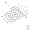
- FIG. 1 is an exploded perspective view showing the configuration of the capacitive input device 10 of the first embodiment.
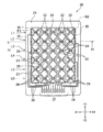
- FIG. 2 is a plan view showing the configuration of the capacitance type sensor unit 20 in the capacitance type input device 10.
- the substrate 21, the electrodes 22 and 23 and the wiring 26 formed on the substrate 21 are shown in FIG.
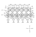
- FIG. 3A is an enlarged view of a portion III in FIG. 2
- FIG. 3B is a plan view showing shapes of a conductive region and a non-conductive region in a modified example.
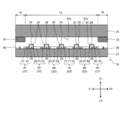
- 4 is a cross-sectional view in a state where the capacitive input device 10 shown in FIG.
- the Z1-Z2 direction is the thickness direction (vertical direction) of the capacitive input device 10
- the XY plane is a plane perpendicular to the Z1-Z2 direction.
- the state of viewing the Z2 side from the Z1 side along the Z1-Z2 direction is referred to as a plan view
- the shape in the plan view is referred to as a planar shape
- the outer shape in the planar shape is referred to as an outer shape.
- the capacitive input device 10 includes a capacitive sensor unit 20 that detects input position information and a front panel 31.
- the front panel 31 is disposed on the input operation side (Z1 direction in FIG. 1) with respect to the capacitive sensor unit 20, and the capacitive sensor unit 20 and the front panel 31 are disposed via an adhesive layer 32. It is pasted together.
- the adhesive layer 32 for example, an optical adhesive (OCA) can be used, and the capacitive sensor unit 20 and the front panel 31 are bonded to each other by OCA.
- OCA optical adhesive
- the front panel 31 is formed in a flat plate shape using a translucent glass material or a resin material.
- a colored and opaque decorative layer 33 is provided by printing or the like on the back surface 31a of the front panel 31 (the surface in the Z2 direction in FIG. 1) (see FIG. 4).
- the decorative layer 33 is provided in a frame shape on the outer peripheral portion of the front panel 31 whose shape viewed from the Z1-Z2 direction is substantially rectangular.
- the front panel 31 and the base material 21 arranged on the back side (Z2 direction side) of the front panel 31 are divided by the decorative layer 33 when viewed along the Z1-Z2 direction.
- the area surrounded by is the input area 15 where the input operation is performed, and the area overlapping with the decoration layer 33 outside the input area 15 is the non-input area 16.
- the front panel 31 is not limited to a flat plate shape as shown in FIG. 1, and may have a three-dimensional surface shape having a curved surface, or a part of the casing of the electronic device may be the front panel 31
- the decorative layer 33 is made of a colored and opaque material, for example, a material made opaque by adding a pigment to an acrylic resin.
- a pigment added to the decoration layer 33 when making it black, carbon black is mentioned, for example.
- the decorative layer 33 is formed so as to cover the wiring 26 when viewed from the front surface 31b side of the front panel 31 over a range in which the wiring 26 is hidden when viewed from the front panel 31 side (see FIG. 4).
- the decorative layer 33 has a combination of color and transparency that makes the wiring 26 invisible when viewed from the front panel 31 side.
- the decoration layer 33 is most preferably black and opaque. However, if the wiring 26 can be made invisible, the decoration layer 33 may have translucency.
- a plurality of first electrodes 22 and a plurality of second electrodes 23 are arranged in the input region 15 of the capacitive sensor unit 20.
- the capacitive sensor unit 20 includes a base material 21, a plurality of first electrodes 22, a plurality of second electrodes 23, and a plurality of wirings 26 formed on the base material surface of the base material 21. Configured.
- the first electrode 22 and the second electrode 23 are pad-shaped electrodes formed in the input region 15 and having a plane extending in the XY plane.
- the first electrodes 22 are arranged at intervals in the X1-X2 direction (first direction), and the first electrodes 22 adjacent in the X1-X2 direction are connected to each other by the bridge portion 24.
- the plurality of connected first electrodes 22 extend in the X1-X2 direction and are spaced apart in the Y1-Y2 direction (second direction) to form a plurality of columns L1, L2, L3, L4, L5. , L6 are arranged.
- the second electrodes 23 are arranged at intervals in the Y1-Y2 direction, and the second electrodes 23 adjacent in the Y1-Y2 direction are connected to each other by a narrow connecting portion 25.
- the plurality of connected second electrodes 23 extend in the Y1-Y2 direction, and a plurality of second electrodes 23 are arranged at intervals in the X1-X2 direction.
- the plurality of connected first electrodes 22 and the plurality of connected second electrodes 23 are arranged so as to cross each other.
- a crossing insulating layer 35 is provided so as to cover the connecting part 25 at a portion where the connecting part 25 and the bridge part 24 intersect, and straddles the connecting part 25 and the crossing insulating layer 35. Accordingly, a bridge portion 24 is formed.
- the first electrodes 22 arranged so as to sandwich the connecting portion 25 in the X1-X2 direction are connected by a bridge portion 24 as a first connecting portion, and the second electrodes 23 are connected by a second connection. It is connected by a connection part 25 as a part.
- the first electrode 22 and the second electrode 23 are formed in a state of being insulated from each other.
- a plurality of wirings 26 connected to the first electrode 22 and the second electrode 23 are formed in the non-input region 16 of the base material 21.
- the plurality of wirings 26 are routed around the non-input area 16 of the base material 21 and connected to a terminal portion 27 for connecting to an external circuit.
- the base material 21 is formed using a film-like non-conductive resin material, and a translucent resin material such as a polycarbonate resin, a polyethylene terephthalate resin, a polyethylene naphthalate resin, a cyclic polyolefin, or a polymethyl methacrylate resin is used. Used.
- the first electrode 22, the second electrode 23, and the connection portion 25 are formed using a light-transmitting conductive material such as ITO (Indium Tin Oxide), SnO 2 , ZnO, etc.
- the thin film method is used.
- the bridge portion 24 is formed using a metal material such as Cu, Ag, Au, an alloy such as CuNi, AgPd, or a conductive oxide material such as ITO.
- a metal material such as Cu, Ag, or Au, or a conductive oxide material such as ITO can be used.
- the first electrode 22 is a reception electrode and the second electrode 23 is a drive electrode, and is driven and detected by a mutual capacitance detection method.
- the second electrode 23 as the drive electrode has a plurality of columns extending along the Y1-Y2 direction, and the voltage of the rectangular wave is constant in order for each column. Applied with a period.
- each column is sequentially connected to the detection circuit. .
- the first electrode 22 includes an end electrode and a plurality of main electrodes for each column extending along the X1-X2 direction.
- FIG. 3A shows the two rows L1 and L2 on the upper side in the Y1 direction in FIG. 2 in an enlarged manner.
- the second row L2 from the top will be described as an example, but the first electrodes 22 of the other five rows L1, L3, L4, L5, and L6 have the same configuration.
- the first electrodes 22 at both ends in the X1-X2 direction are end electrodes 40, 90, and these two end portions in the X1-X2 direction.
- the four first electrodes 22 between the electrodes 40 and 90 are the main electrodes 50, 60, 70 and 80.
- four main electrodes 50, 60, 70, 80 are arranged between the two end electrodes 40, 90.
- the number of main electrodes is the capacitance type input device. It can be set arbitrarily according to the specifications of
- the outer shape (outer planar shape) of the first electrode 22 in plan view is a rhombus shape in the main electrodes 50, 60, 70, and 80.
- the end electrode 40 on the X1 side has a triangular shape in which the outer region on the X1 side is missing among the rhombuses similar to the main electrodes 50, 60, 70, 80, and the end on the X2 side
- the partial electrode 90 has a triangular shape in which the outer region on the X2 side is missing among the rhombuses similar to the main electrodes 50, 60, 70, and 80. In either case, the end electrodes 40 and 90 are formed smaller than the main electrodes 50, 60, 70 and 80.
- Each of the end electrodes 40, 90 and the main electrodes 50, 60, 70, 80 includes a non-conductive region and a conductive region surrounding the non-conductive region. Specifically, as shown in FIG. 4, by forming a hole portion penetrating in the Z1-Z2 direction at a predetermined position of the end electrode 40 having a triangular outer shape, the hole portion is formed into a non-conductive region.
- Reference numeral 41 denotes an electrode portion surrounding the conductive region 42.
- the non-conductive regions 51, 61, 71, 81, 91 is formed, and electrode portions surrounding it are made conductive regions 52, 62, 72, 82, 92.
- the nonconductive region may be formed as a layer of a nonconductive material, or the hole may be filled with a nonconductive material.
- the non-conductive regions 51, 61, 71, 81 in the main electrodes 50, 60, 70, 80 have a rhombus shape similar to the main electrodes 50, 60, 70, 80.
- Each has a planar shape.
- the outer planar shape of the main electrodes 50, 60, 70, 80 is symmetrical in the Y1-Y2 direction and the X1-X2 direction, and in each case, the intersection of two diagonal lines is the center of gravity 50g in the planar shape. , 60 g, 70 g, and 80 g.
- non-conductive regions 51, 61, 71, 81 also have plane shapes that are symmetrical in the Y1-Y2 direction and the X1-X2 direction, respectively, and in each case, the intersection of two diagonal lines is the center of gravity 51g in the plane shape. 61g, 71g and 81g.
- the conductive regions 52, 62, 72, and 82 are also set with centroids 52g, 62g, 72g, and 82g, respectively, based on their planar shapes.
- the non-conductive region 41 in the end electrode 40 on the X1 side has a triangular planar shape that is similar to the end electrode 40.
- the end electrode 40 is disposed so as to straddle the boundary B1 between the input region 15 and the non-input region 16 in the X1-X2 direction, and the non-conductive region 41 has a triangular shape that expands toward the X1 side.
- the boundary B1 is a boundary extending along the Y1-Y2 direction on the X1 side among the boundaries of the input area 15 and the non-input area 16.
- the end electrode 40 has a triangular shape in which the outer region on the X1 side is missing, and the missing region overlaps the non-input region 16.
- the rhombus including the virtual outer shape 40a and the rhombus including the virtual outer shape 41a are respectively symmetric in the Y1-Y2 direction and the X1-X2 direction, and in each case, the intersection of two diagonal lines is The center of gravity 40g and 41g in the virtual outer shape plane shape are obtained.
- the conductive region 42 also has a center of gravity 42g based on a virtual outer shape plane shape.
- the nonconductive region 91 has a triangular planar shape similar to the end electrode 90 (FIG. 3A )).
- the end electrode 90 is disposed so as to straddle the boundary B2 between the input region 15 and the non-input region 16 in the X1-X2 direction, and the nonconductive region 91 has a triangular shape that expands toward the X2 side.
- the boundary B2 is a boundary extending along the Y1-Y2 direction on the X2 side among the boundaries between the input area 15 and the non-input area 16.
- the end electrode 90 has a triangular shape in which the outer region on the X2 side is missing, and the missing region overlaps the non-input region 16.
- the virtual outer shape 90a that supplements the end electrode 90 is indicated by a broken line
- the non-conductive region 91 is a rhombus similar to the non-conductive regions 51, 61, 71, 81 of the main electrodes 50, 60, 70, 80
- a virtual outline that supplements the non-conductive region 91 The shape 91a is indicated by a broken line.
- the rhombus including the virtual outer shape 90a and the rhombus including the virtual outer shape 91a are symmetric in the Y1-Y2 direction and the X1-X2 direction, respectively, and in each of the intersections of two diagonal lines,
- the center of gravity is 90 g and 91 g in the virtual outer shape plane shape.
- the conductive region 92 also has a center of gravity 92g based on a virtual outer shape plane shape.
- the position of the center of gravity of the main electrodes 50, 60, 70, 80 and the end electrodes 40, 90 will be described.
- the positions of the centers of gravity 52g, 62g, 72g, 82g of the conductive regions 52, 62, 72, 82 are at the ends in the X1-X2 direction (first direction).
- the closer electrode is set on the side farther from the end. That is, in the most X1-side main electrode 50, the position of the center of gravity 52g of the conductive region 52 in the main electrode 50 is compared with the position of the center of gravity 62g of the conductive region 62 of the inner main electrode 60 in the main electrode 60. It is away from the end X1.
- the position of the center of gravity 82g of the conductive region 82 of the main electrode 80 on the most X2 side in the main electrode 80 is compared with the position of the center of gravity 72g of the conductive region 72 of the inner main electrode 70 on the main electrode 70, It is away from the end X2.
- the center of gravity 52g, 62g, 72g, and 82g of each of the conductive regions 52, 62, 72, and 82 of the main electrodes 50, 60, 70, and 80 are larger in the main electrode that is farther from the end electrodes 40 and 90.
- the main electrode is arranged near the center of gravity or at the same position.
- the positions of the center of gravity 52g, 62g, 72g, 82g of each of the conductive regions 52, 62, 72, 82 are such that the main electrode closer to the end in the X1-X2 direction corresponds to the corresponding main electrode 50, It is set on the side far from the end with respect to the center of gravity 50g, 60g, 70g, 80g of 60, 70, 80.
- the electrode closer to the end in the X1-X2 direction (first direction) is arranged on the end side.
- the position of the center of gravity 42g of the conductive region is in the X1-X2 direction (from the position of the center of gravity 52g of the conductive region 52 in the adjacent main electrode 50 ( It is set on the side far from the end in the first direction), that is, on the X2 side.
- the distance between the center of gravity 42g of the conductive region and the center of gravity 40g of the end electrode 40 is longer than the distance between the center of gravity 52g of the conductive region 52 in the adjacent main electrode 50 and the center of gravity 50g of the main electrode 50. Is set.
- the position of the center of gravity 92g of the conductive region is smaller than the position of the center of gravity 82g of the conductive region 82 of the adjacent main electrode 80 by X1 ⁇ . It is set on the far side from the end in the X2 direction, that is, on the X1 side.
- the conductive regions and the non-conductive regions are arranged in the main electrodes 50, 60, 70, 80 and the end electrodes 40, 90, the main electrodes 50 adjacent to the end electrodes 40, 90, respectively. 80, the center of gravity of the conductive region is arranged at a position farther from the adjacent end electrodes 40, 90 than the center of gravity of the main electrode. Therefore, the conductive region on the side of the end electrodes 40 and 90 is set smaller than when the main electrode is not provided with a non-conductive region or when the non-conductive region is provided at the center of the main electrode.
- the input position can be accurately detected even when the detection target comes into contact with or approaches the end of the input region 15. This is the same when an input operation is performed over the opposite end electrode 90 and the adjacent main electrode 80.
- the electrode closer to the end in the X1-X2 direction (first direction) is on the side farther from the end.
- the positions of the respective centers of gravity 42g, 52g, 62g, 72g, 82g, and 92g are gradually inward in the X1-X2 direction from the inner main electrodes 60 and 70 toward the outer electrodes, that is, the main electrodes. It is arranged so as to shift to a position close to the center of gravity.
- the arrangement balance of the conductive regions between the two electrodes adjacent in the X1-X2 direction can be made substantially uniform over the entire X1-X2 direction. Therefore, in addition to the improvement in detection accuracy at both ends of the input region 15, it is possible to sufficiently ensure detection accuracy in the region between both ends.
- the shape of the nonconductive region is similar to the corresponding electrode, that is, a rhombus or a triangle.
- the center of gravity of the planar shape of the conductive region and the nonconductive region is used.
- the planar shape of the non-conductive region may be circular.
- FIG.3 (b) is a top view which shows the shape of the electroconductive area
- the planar shape of the conductive regions 102, 112, 122, 132 is rhombus, and the non-conductive regions 101,
- the planar shape of 111, 121, 131 is circular.
- the number of non-conductive regions may be plural as long as the positions of the center of gravity of the planar shape of the conductive regions and the non-conductive regions can be made the same as in the first embodiment.
- FIG. 5 is an enlarged plan view showing a part of the configuration of the capacitive sensor unit in the modification of the first embodiment shown in FIGS. 1 to 4, and shows a range corresponding to FIG. FIG.
- the second electrode 23 is connected to each other by the connection portion 25 as the second connection portion, and the bridge portion 24 (first connection) straddling the connection portion 25 and the crossing insulating layer 35. Part) to connect the first electrodes 22 to each other.
- the first electrodes 22 are connected to each other by a connection portion 124 as a first connection portion, and the connection portion 124 and the connection portion 124 are covered.
- a configuration is also possible in which the second electrodes 23 are connected to each other by a bridge portion 125 (second connection portion) straddling the intersection insulating layer. As a result, it is not necessary to secure a connection area between the first electrode 22 and the bridge portion 125, and the degree of freedom in adjusting the conductive region and the non-conductive region can be improved.
- FIG. 6 is a diagram illustrating the configuration of the capacitive sensor section 220 of the capacitive sensor according to the second embodiment of the present invention.
- the display of the non-conductive region is omitted.
- two transparent electrode members that is, the first transparent electrode member 400a and the second transparent electrode member 400b are normal to the first surfaces S21 and S22, respectively.
- the laminated transparent electrode member 600 is laminated along the direction (Z1-Z2 direction).
- the first transparent electrode member 400a includes a plurality of second electrodes along the X1-X2 direction (first direction) on the first surface S21 on the upper side (Z1 side) as in the first embodiment shown in FIG.
- the first electrodes 222 are arranged at intervals and are connected to each other by the first connection portion 224.
- the plurality of connected first electrodes 222 extend in the X1-X2 direction and are spaced in the Y1-Y2 direction (second direction) to connect the four rows L21, L22, L23, L24. Forming.
- a plurality of second electrodes 223 are provided at intervals along the Y1-Y2 direction (second direction) on the first surface S22 on the upper side (Z1 side). Arranged and connected to each other by a second connection 225.
- the planar shape and arrangement of the first electrode 222 and the second electrode 223 are the same as those of the first electrode 22 and the second electrode 23 in the first embodiment.
- FIG. 8 is an enlarged view of the VIII portion of FIG. 6 in the configuration in which the first transparent electrode member 400a and the second transparent electrode member 400b in the second embodiment are stacked along the Z1-Z2 direction.
- FIG. 8 is an enlarged view of the VIII portion of FIG. 6 in the configuration in which the first transparent electrode member 400a and the second transparent electrode member 400b in the second embodiment are stacked along the Z1-Z2 direction.
- FIG. As described above, the planar shape and arrangement of the first electrode 222 and the second electrode 223 are the same as those of the first electrode 22 and the second electrode 23 in the first embodiment.
- the non-conductive region, the conductive region, the boundary, and the like are indicated using the same reference numerals as in the first embodiment.
- FIG. 7 is a diagram illustrating the configuration of the capacitive sensor section 320 of the capacitive sensor according to the third embodiment of the present invention. Also in FIG. 7, the display of the non-conductive region is omitted.
- the capacitive sensor unit 320 shown in FIG. 7 includes a plurality of first electrodes on the first surface S31 on the upper side (Z1 side) of the two main surfaces of the sheet-like base material 21 as the transparent electrode member 500.
- An electrode 322 is provided, and a plurality of second electrodes 323 are provided on the lower (Z2 side) second surface S32.
- the plurality of first electrodes 322 are arranged at intervals along the X1-X2 direction (first direction), and are connected to each other by the first connection portion 324.
- the plurality of connected first electrodes 322 extend in the X1-X2 direction and are spaced in the Y1-Y2 direction (second direction) to connect the four rows L31, L32, L33, L34.
- the plurality of second electrodes 323 are arranged at intervals along the Y1-Y2 direction (second direction) and are connected to each other by the second connection portion 325.
- the present invention since the planar shape and arrangement of the first electrode 322 and the second electrode 323 are the same as those of the first electrode 22 and the second electrode 23 in the first embodiment, the IX portion of FIG. 7 is enlarged. Then, it becomes the structure similar to the structure shown in FIG.
- the present invention has been described with reference to the above embodiment, the present invention is not limited to the above embodiment, and can be improved or modified within the scope of the purpose of the improvement or the idea of the present invention.
- Example> simulation results in Examples and Comparative Examples will be described.
- the first electrode and the second electrode are configured as shown in FIG. 6, that is, the plurality of first electrodes 222 and the plurality of electrodes.
- a capacitance type input device having a capacitance type sensor unit having a configuration in which two transparent electrode members 400a and 400b each having a second electrode 223 formed thereon are laminated is used as a model.
- the planar shape of the first electrode 222 and the second electrode 223 has a distance of 5 mm (excluding the end electrode 222a) in the X1-X2 direction and the Y1-Y2 direction. Is 5 mm) (see FIGS.
- the planar shape of the end electrode 222a was a triangle cut in the Y1-Y2 direction by a line connecting the upper and lower diagonals of the rhombus.
- the arrangement pitch of these electrodes was 6 mm in both the X1-X2 direction and the Y1-Y2 direction.
- FIG. 9A is an enlarged plan view showing a part of the capacitance type sensor unit in the comparative example.
- each of the first electrode 222 and the second electrode 223 is composed only of a conductive region, and a non-conductive region is not provided. Absent.
- FIG. 9B is an enlarged plan view illustrating a part of the capacitive sensor unit according to the first embodiment.
- each of the main electrodes 222b, 222c, 222d, and 222e of the first electrode 222 has a diagonal distance of 2.5 mm (each length in the X1-X2 direction and the Y1-Y2 direction). Is 2.5 mm), and has a configuration in which non-conductive regions 232, 233, 234, and 235 having a rhombus shape similar to the corresponding first electrode are provided (see FIG. 9B). ).
- the first electrode 222 having a right isosceles triangle, which is the end electrode 222a, is also provided with a non-conductive region 231 having an area of 1/4 and similar to the end electrode 222a.
- the diamond-shaped non-conductive regions 232, 233, 234, and 235 provided on the diamond-shaped first electrode 222 are as follows from the side proximal to the end electrode 222a. Arranged. (1)
- the second proximal electrode 222c to the end electrode 222a, the third proximal electrode 222d, and the fourth proximal electrode 222e (the most distal electrode from the end electrode):
- the centroids 233g, 234g, and 235g of the non-conductive regions 233, 234, and 235 overlap with the centroids 222cg, 222dg, and 222eg of the corresponding first electrodes 222c, 222d, and 222e, respectively.
- FIG. 9C is a plan view illustrating a part of the capacitance type sensor unit in Example 2 in an enlarged manner.
- each of the main electrodes 222b, 222c, 222d, and 222e in the first electrode 222 has a diagonal distance of 2.5 mm, and the corresponding electrode.
- a non-conductive region 242, 243, 244, 245 having a rhombus shape similar to that of FIG. 9 (see FIG. 9C).
- the non-conductive region 241 having an area of 1 ⁇ 4 and similar to the end electrode 222a was also provided in the first electrode 222 having a right isosceles triangle of the end electrode 222a.
- the diamond-shaped non-conductive regions 242, 243, 244, and 245 provided on the diamond-shaped first electrode 222 are as follows from the side proximal to the end electrode 222 a. Arranged. (1) The nearest electrode 222b to the end electrode 222a: The center of gravity 242g of the non-conductive region 242 is closer to the end electrode 222a by 1.25 mm than the center of gravity 222bg of the corresponding first electrode 222b (FIG. 9C ) In the X1-X2 direction X1 side).
- Electrode 222c second closest to the end electrode 222a the center of gravity 243g of the non-conductive region 243 is closer to the end electrode 222a by 1.0 mm than the center of gravity 222cg of the corresponding first electrode 222c (see FIG. 9 (c), X1-X2 direction X1 side).
- Electrode 222d third proximal to the end electrode 222a the center of gravity 244g of the non-conductive region 244 is closer to the end electrode 222a by 0.5 mm than the center of gravity 222dg of the corresponding first electrode 222d (see FIG. 9 (c), X1-X2 direction X1 side).
- the contact area of the finger which is the object to be detected, is assumed to be a circle having a diameter of about 6 mm.
- the detection position error at the end was as follows. (Comparative example) 1.275 mm (Example 1) 0.95 mm (Example 2) 0.95 mm
- the capacitance type input device of Example 1 and the capacitance type input device of Example 2 having the configuration of the present invention are compared with the capacitance type input device according to the comparative example.
- the detection position error of the end portion is reduced by about 25%, and this confirms the effect of the present invention that the input position can be accurately detected even when the input operation is performed at the end portion of the input area.
- the capacitive input device according to the present invention is useful in that the input position can be accurately detected even when an input operation is performed at the end of the input region.
Landscapes
- Engineering & Computer Science (AREA)
- General Engineering & Computer Science (AREA)
- Theoretical Computer Science (AREA)
- Human Computer Interaction (AREA)
- Physics & Mathematics (AREA)
- General Physics & Mathematics (AREA)
- Microelectronics & Electronic Packaging (AREA)
- Structure Of Printed Boards (AREA)
- Position Input By Displaying (AREA)
Abstract
入力領域の端部において入力操作を行う場合においても入力位置を正確に検出することができる本発明の静電容量式入力装置は、複数の第1の電極が基材面内の第1の方向において間隔を設けて配置され、複数の第2の電極が第1の方向に交差する第2の方向において間隔を設けて配置されており、複数の第1の電極は、第1の方向に位置する端部電極と、端部電極から離れる方向に沿って位置する複数の主電極とを備え、端部電極の外形平面形状は、主電極の外形平面形状に対して、主電極よりも小さい形状を有し、複数の第1の電極はそれぞれ、平面視において、導電性領域と非導電性領域を有し、端部電極に隣り合う主電極において、導電性領域の重心は、その主電極の重心よりも、隣り合う端部電極から離れる方向に配置される。
Description
本発明は、操作者が入力領域に指などを接触又は近づけたときに、その位置情報を検出する静電容量式入力装置に関する。
特許文献1や特許文献2に記載の静電容量式の入力装置は、基材の入力領域に、第1の方向において間隔を設けて配置された複数の第1の電極と、第1の方向に交差する第2の方向において間隔を設けて配置された複数の第2の電極と、が形成され、さらに、非入力領域に、第1の電極と第2の電極にそれぞれ接続された配線が形成されている。第1の電極と第2の電極は、その間で静電容量を形成するように配置されており、操作者が入力操作を行う際に、入力領域に指などの被検出体を接触させて、又は、接触させずに近づけた場合に、第1の電極と第2の電極との間の静電容量と、各電極と被検出体との間に形成される静電容量とが結合し、この静電容量の変化に基づいて入力位置情報が検出される。
特許文献1や特許文献2に記載の入力装置では、平面サイズの小型化の要請により、第1の方向の両端部において2つの第1の電極が設けられる領域に、第2の方向に沿って入力領域と非入力領域の境界線が設定されている。このため、上記両端部の2つの第1の電極は、非入力領域側が欠けた略三角形の平面形状で形成される。これに対して、第1の方向の両端部の2つの第1の電極に挟まれた複数の第1の電極は、平面視略ひし形で互いに同一の形状で形成されている。
しかしながら、上記入力装置において、端部の第1の電極の面積が、これに隣り合う第1の電極の面積の半分程度であるため、入力領域の端部やその近傍において入力操作を行う場合、被検出体が互いに隣り合う2つの第1の電極に接触又は近接したにもかかわらず、面積が大きな方の第1の電極のみに接触又は近づいたものとして検出されたり、又は、面積が大きな方の第1の電極において実際よりも広い範囲に接触又は近接したものとして検出されることがあり、実際の操作位置とは異なる位置が入力位置として検出されてしまうおそれがあった。
そこで本発明は、入力領域の端部において入力操作を行う場合においても入力位置を正確に検出することができる静電容量式入力装置を提供することを目的とする。
上記課題を解決するために、本発明の静電容量式入力装置は、基材面上に、複数の電極と、複数の電極に接続された配線とが形成された静電容量式入力装置であって、複数の電極は入力操作を行う入力領域に形成され、配線は入力領域の外側に設定された非入力領域に形成されており、複数の電極は、透光性の複数の第1の電極及び複数の第2の電極を有して構成され、複数の第1の電極は基材面内の第1の方向において間隔を設けて配置され、複数の第2の電極は第1の方向に交差する第2の方向において間隔を設けて配置されており、複数の第1の電極同士が第1の接続部によって接続され、複数の第2の電極同士が第2の接続部によって接続され、第1の電極と第2の電極は互いに絶縁され、複数の第1の電極は、第1の方向の端部に位置する端部電極と、端部電極から離れる方向に沿って位置する複数の主電極とを備え、端部電極の外形平面形状は、主電極の外形平面形状に対して、主電極よりも小さい形状を有し、複数の第1の電極はそれぞれ、平面視において、導電性領域と非導電性領域を有し、端部電極に隣り合う主電極において、導電性領域の重心は、その主電極の重心よりも、隣り合う端部電極から離れる方向に配置されたことを特徴としている。
これにより、入力領域の端部において入力操作が行われ、被検出体が接触し、又は、近づいた場合にも、その入力位置を正確に検出することが可能となる。
これにより、入力領域の端部において入力操作が行われ、被検出体が接触し、又は、近づいた場合にも、その入力位置を正確に検出することが可能となる。
本発明の静電容量式入力装置では、複数の主電極において、導電性領域の重心は、端部電極から遠い主電極の方が、その主電極の重心に近い位置に配置されることが好ましい。
これにより、第1の方向において隣り合う2つの電極間の導電性領域の配置バランスを、第1の方向の全体に渡ってほぼ均等にすることができる。よって、入力領域の両端部の検出精度の向上に加えて、両端部の間の領域における検出精度も十分に確保することができる。
これにより、第1の方向において隣り合う2つの電極間の導電性領域の配置バランスを、第1の方向の全体に渡ってほぼ均等にすることができる。よって、入力領域の両端部の検出精度の向上に加えて、両端部の間の領域における検出精度も十分に確保することができる。
本発明の静電容量式入力装置では、端部電極において、主電極と同じ仮想の外形平面形状を想定したとき、仮想の外形平面形状において、導電性領域の重心と、その端部電極の重心との距離は、隣り合う主電極における導電性領域の重心と、その主電極の重心との距離よりも長いことが好ましい。
これにより、端部電極において隣り合う主電極側に、検出のために十分な面積の導電性領域を確保することができるため、入力領域の端部において、入力操作を行う場合にも、その入力位置を正確に検出することが可能となる。
なお、端部電極において、検出のために十分な導電性領域を確保できる場合には、その導電性領域の重心と、端部電極の重心との距離は、隣り合う主電極における導電性領域の重心と、その主電極の重心との距離と同程度であってもよい。
これにより、端部電極において隣り合う主電極側に、検出のために十分な面積の導電性領域を確保することができるため、入力領域の端部において、入力操作を行う場合にも、その入力位置を正確に検出することが可能となる。
なお、端部電極において、検出のために十分な導電性領域を確保できる場合には、その導電性領域の重心と、端部電極の重心との距離は、隣り合う主電極における導電性領域の重心と、その主電極の重心との距離と同程度であってもよい。
本発明の静電容量式入力装置では、第1の接続部は、第2の接続部を覆うように形成された交差部絶縁層を跨がって形成されたブリッジ部を備え、又は、第2の接続部は、第1の接続部を覆うように形成された交差部絶縁層を跨がって形成されたブリッジ部を備えることが好ましい。
これにより、入力位置の検出精度を確保しつつ、第1の電極と第2の電極を効率的に配置することができる。
これにより、入力位置の検出精度を確保しつつ、第1の電極と第2の電極を効率的に配置することができる。
本発明の静電容量式入力装置では、複数の第2の電極は駆動電極であり、複数の第1の電極は受信電極であることが好ましい。
これにより、入力領域の端部において、端部電極と、これと隣り合う主電極との間で静電容量が確実に形成されるため、入力領域の端部において入力操作を行った場合にも、その入力位置を正確に検出することが可能となる。
これにより、入力領域の端部において、端部電極と、これと隣り合う主電極との間で静電容量が確実に形成されるため、入力領域の端部において入力操作を行った場合にも、その入力位置を正確に検出することが可能となる。
本発明の静電容量式入力装置では、主電極の外形平面形状はひし形状であって、その非導電性領域の平面形状もひし形状であり、端部電極の外形平面形状は三角形状であって、その非導電性領域の平面形状も三角形状であることが好ましい。
これにより、主電極と端部電極の配置や製造を容易に行うことができる。
これにより、主電極と端部電極の配置や製造を容易に行うことができる。
本発明の静電容量式入力装置では、端部電極において、第1の方向の外側の領域は、非入力領域に重なっていることが好ましい。
これにより、非入力領域を所望の範囲に設定して静電容量式入力装置の小型化を図りつつ、入力領域の端部における検出精度を確保することができる。
これにより、非入力領域を所望の範囲に設定して静電容量式入力装置の小型化を図りつつ、入力領域の端部における検出精度を確保することができる。
本発明によると、入力領域の端部において入力操作を行う場合においても入力位置を正確に検出することができる。
以下、本発明の実施形態に係る静電容量式入力装置について図面を参照しつつ詳しく説明する。
<第1実施形態>
図1は、第1実施形態の静電容量式入力装置10の構成を示す分解斜視図である。図2は、静電容量式入力装置10における静電容量式センサ部20の構成を示す平面図であり、基材21、並びに、基材21に形成された各電極22、23及び配線26を示す平面図である。図3(a)は図2のIII部分の拡大図、(b)は変形例における導電性領域と非導電性領域の形状を示す平面図である。図4は、図1に示す静電容量式入力装置10を組み立てた状態の断面図であって、図2のIV-IV線の位置で切断して矢印方向から見た断面図である。図1~図4においては、基準座標としてX-Y-Z座標が示されている。Z1-Z2方向は静電容量式入力装置10の厚み方向(上下方向)であり、XY平面はZ1-Z2方向に垂直な平面である。以下の説明において、Z1-Z2方向に沿ってZ1側からZ2側を見た状態を平面視と称し、平面視における形状を平面形状、平面形状における外形形状を外形平面形状と述べる。
<第1実施形態>
図1は、第1実施形態の静電容量式入力装置10の構成を示す分解斜視図である。図2は、静電容量式入力装置10における静電容量式センサ部20の構成を示す平面図であり、基材21、並びに、基材21に形成された各電極22、23及び配線26を示す平面図である。図3(a)は図2のIII部分の拡大図、(b)は変形例における導電性領域と非導電性領域の形状を示す平面図である。図4は、図1に示す静電容量式入力装置10を組み立てた状態の断面図であって、図2のIV-IV線の位置で切断して矢印方向から見た断面図である。図1~図4においては、基準座標としてX-Y-Z座標が示されている。Z1-Z2方向は静電容量式入力装置10の厚み方向(上下方向)であり、XY平面はZ1-Z2方向に垂直な平面である。以下の説明において、Z1-Z2方向に沿ってZ1側からZ2側を見た状態を平面視と称し、平面視における形状を平面形状、平面形状における外形形状を外形平面形状と述べる。
図1に示すように、静電容量式入力装置10は、入力位置情報を検出する静電容量式センサ部20と、表面パネル31とを有して構成される。表面パネル31は、静電容量式センサ部20に対して入力操作側(図1のZ1方向)に配置されており、静電容量式センサ部20と表面パネル31とは粘着層32を介して貼り合わされる。ここで、粘着層32としては、例えば光学接着剤(OCA)を用いることができ、OCAによって、静電容量式センサ部20と表面パネル31とを互いに接着させる。
表面パネル31は、透光性のガラス材料又は樹脂材料を用いて平板状に形成されている。表面パネル31の裏面31a(図1のZ2方向の面)(図4参照)には有色で不透明の加飾層33が印刷等によって設けられている。この加飾層33は、Z1-Z2方向から見た形状が略矩形状である表面パネル31の外周部において枠状に設けられている。表面パネル31、及び、表面パネル31の裏側(Z2方向側)に配置された基材21は、Z1-Z2方向に沿って見たとき、加飾層33によって区分けされており、加飾層33に囲まれた領域が入力操作を行う入力領域15であり、入力領域15の外側の加飾層33と重なる領域が非入力領域16である。
なお、表面パネル31は図1に示すような平板状に限定されず、曲面を有する立体的な表面形状を有するものとしても良いし、電子機器の筐体の一部を表面パネル31としても良い。
なお、表面パネル31は図1に示すような平板状に限定されず、曲面を有する立体的な表面形状を有するものとしても良いし、電子機器の筐体の一部を表面パネル31としても良い。
加飾層33は、有色で不透明な材料、例えば、アクリル系樹脂に顔料を添加して不透明とした材料を用いる。加飾層33に添加する顔料としては、黒色にする場合は例えばカーボンブラックが挙げられる。
加飾層33は、表面パネル31の表面31b側から見て配線26を覆うように、別言すると、表面パネル31側から見て配線26が隠されるような範囲に渡って形成される(図4参照)。また、加飾層33は、表面パネル31側から見て、配線26を視認不可能とするような色及び透明度の組み合わせを有する。例えば、加飾層33を黒色で不透明とすることが最も好ましいが、配線26を視認不可能とすることができれば、透光性を持たせても良い。
図1と図2に示すように、静電容量式センサ部20の入力領域15には複数の第1の電極22及び複数の第2の電極23が配列されている。
静電容量式センサ部20は、基材21と、基材21の基材面上に形成された複数の第1の電極22、複数の第2の電極23、及び、複数の配線26を有して構成される。第1の電極22及び第2の電極23は入力領域15に形成された、XY平面に広がる平面を有するパッド状の電極である。
静電容量式センサ部20は、基材21と、基材21の基材面上に形成された複数の第1の電極22、複数の第2の電極23、及び、複数の配線26を有して構成される。第1の電極22及び第2の電極23は入力領域15に形成された、XY平面に広がる平面を有するパッド状の電極である。
第1の電極22は、X1-X2方向(第1の方向)に間隔を設けて配置されており、X1-X2方向に隣り合う第1の電極22同士はブリッジ部24によって互いに接続される。接続された複数の第1の電極22は、X1-X2方向において延在するとともに、Y1-Y2方向(第2の方向)において間隔を設けて、複数の列L1、L2、L3、L4、L5、L6の6本が配列されている。
第2の電極23はY1-Y2方向において間隔を設けて配列されており、Y1-Y2方向に隣り合う第2の電極23同士は幅細の接続部25によって互いに接続されている。接続された複数の第2の電極23は、Y1-Y2方向において延在するとともに、X1-X2方向において間隔を設けて複数本配列されている。
図2に示すように、接続された複数の第1の電極22と、接続された複数の第2の電極23とは、互いに交差するように配置されている。図4に示すように、接続部25とブリッジ部24とが交差する部分において、接続部25を覆うように交差部絶縁層35が設けられており、接続部25及び交差部絶縁層35を跨がってブリッジ部24が形成されている。接続部25をX1-X2方向に挟むように配置された第1の電極22同士は、第1の接続部としてのブリッジ部24によって接続されており、第2の電極23同士は第2の接続部としての接続部25によって接続されている。このように、第1の電極22と第2の電極23とは、互いに絶縁された状態で形成される。
図2に示すように、基材21の非入力領域16には、第1の電極22及び第2の電極23にそれぞれ接続された複数の配線26が形成されている。これらの複数の配線26は、基材21の非入力領域16を引き回されて、外部回路と接続するための端子部27に接続される。
基材21は、フィルム状の非導電性の樹脂材料を用いて形成されており、ポリカーボネート樹脂、ポリエチレンテレフタレート樹脂、ポリエチレンナフタレート樹脂、環状ポリオレフィン、ポリメタクリル酸メチル樹脂等の透光性樹脂材料が用いられる。第1の電極22、第2の電極23、及び、接続部25は、ITO(Indium Tin Oxide)、SnO2、ZnO等の透光性の導電材料を用いて形成されており、スパッタや蒸着等の薄膜法により形成される。また、ブリッジ部24は、Cu、Ag、Au等の金属材料やCuNi、AgPd等の合金、ITO等の導電性酸化物材料を用いて形成される。配線26及び端子部27には、Cu、Ag、Au等の金属材料やITO等の導電性酸化物材料を用いることができる。
静電容量式センサ部20においては、第1の電極22が受信電極とされ、第2の電極23が駆動電極とされており、相互容量検出方式で駆動・検出される。すでに述べたように、駆動電極としての第2の電極23は、Y1-Y2方向に沿って延在する列が複数本形成されており、それぞれの列に対して順番に矩形波の電圧が一定周期で印加される。一方、X1-X2方向に沿って延在する6本の列L1、L2、L3、L4、L5、L6が形成された第1の電極22においては、それぞれの列が順に検出回路に接続される。
駆動電極である第2の電極23に電圧が印加されると、矩形波の立ち上がりと立ち下がりのタイミングで、検出電極である第1の電極22に電流が流れる。このときの電流量は、隣り合う2つの第1の電極22間の静電容量によって決められる。操作者が入力操作を行う際に、表面パネル31の表面31bの入力領域15に指や手などの被検出体を接触させて、又は、近づけた場合、隣り合う2つの第1の電極22の間の静電容量に、これら2つの第1の電極22と被検出体との間に形成される静電容量が結合する。このため、被検出体が接触し、又は近づいた第1の電極22において静電容量に変化が生じるため、この静電容量変化に基づいて被検出体による入力位置情報が検出される。
第1の電極22は、X1-X2方向に沿って延在する列ごとに、端部電極と複数の主電極とを備える。図3(a)には、図2のY1方向上側の2本の列L1、L2が拡大して示されている。以下の説明では、上から2つめの列L2を例にとって説明するが、それ以外の5本の列L1、L3、L4、L5、L6の第1の電極22も同様の構成を備える。
図3(a)に示すように、X1-X2方向(第1の方向)の両端部の第1の電極22は、端部電極40、90であり、X1-X2方向においてこれら2つの端部電極40、90の間の4つの第1の電極22が主電極50、60、70、80である。
なお、第1実施形態においては、2つの端部電極40、90の間に4つの主電極50、60、70、80が配置されているが、主電極の数は、静電容量式入力装置の仕様などに応じて任意に設定することができる。
なお、第1実施形態においては、2つの端部電極40、90の間に4つの主電極50、60、70、80が配置されているが、主電極の数は、静電容量式入力装置の仕様などに応じて任意に設定することができる。
平面視における第1の電極22の外形形状(外形平面形状)は、主電極50、60、70、80ではひし形状となっている。これに対して、X1側の端部電極40は、主電極50、60、70、80と同様のひし形のうち、X1側の外側の領域が欠けた三角形状であり、また、X2側の端部電極90は、主電極50、60、70、80と同様のひし形のうち、X2側の外側の領域が欠けた三角形状となっている。いずれも、端部電極40、90が主電極50、60、70、80よりも小さく形が形成されている。
端部電極40、90及び主電極50、60、70、80は、それぞれ、非導電性領域と、それを囲む導電性領域とを備えている。具体的には、図4に示すように、三角形状の外形平面形状の端部電極40の所定位置にZ1-Z2方向に貫通した穴部を形成することにより、この穴部を非導電性領域41とし、それを囲む電極部分を導電性領域42としている。これと同様に、主電極50、60、70、80及び端部電極90のそれぞれにおいて、Z1-Z2方向に貫通した穴部を形成することにより、非導電性領域51、61、71、81、91を形成し、それを囲む電極部分を導電性領域52、62、72、82、92としている。
なお、非導電性領域は、非導電性材料の層として形成し、又は、前記穴部を非導電性材料で満たす形態でもよい。
なお、非導電性領域は、非導電性材料の層として形成し、又は、前記穴部を非導電性材料で満たす形態でもよい。
図3(a)に示すように、主電極50、60、70、80における非導電性領域51、61、71、81は、主電極50、60、70、80と相似形となるひし形状の平面形状をそれぞれ有する。主電極50、60、70、80の外形平面形状は、Y1-Y2方向及びX1-X2方向においてそれぞれ対称な形状となっており、それぞれにおいて、2本の対角線の交点が、平面形状における重心50g、60g、70g、80gとなる。また、非導電性領域51、61、71、81についても、Y1-Y2方向及びX1-X2方向においてそれぞれ対称な平面形状を有し、それぞれにおいて、2本の対角線の交点が平面形状における重心51g、61g、71g、81gとなる。また、導電性領域52、62、72、82も、その平面形状に基づいて重心52g、62g、72g、82gがそれぞれ設定される。
図3(a)に示すように、X1側の端部電極40における非導電性領域41は、端部電極40と相似形となる三角形状の平面形状を有する。端部電極40は、X1-X2方向において、入力領域15と非入力領域16の境界B1を跨ぐように配置され、非導電性領域41はX1側へ行くほど広がる三角形状をなしている。ここで、境界B1は、入力領域15と非入力領域16の境界のうち、X1側においてY1-Y2方向に沿って延びる境界である。端部電極40は、X1側の外側の領域が欠けた三角形状をなしており、欠けた領域は非入力領域16に重なっている。
図3(a)において、端部電極40の外形形状が主電極50、60、70、80と同様のひし形であると想定したとき、端部電極40を補う仮想外形形状40aを破線で示し、また、非導電性領域41が主電極50、60、70、80の非導電性領域51、61、71、81と同様のひし形であると想定したときに、非導電性領域41を補う仮想外形形状41aを破線で示している。仮想外形形状40aを含むひし形、及び、仮想外形形状41aを含むひし形は、それぞれ、Y1-Y2方向及びX1-X2方向において対称な形状となっており、それぞれにおいて、2本の対角線の交点が、仮想の外形平面形状における重心40g、41gとなる。また、導電性領域42も、仮想の外形平面形状に基づいて重心42gが設定される。
一方、X2側の端部電極90においてもX1側の端部電極40と同様に、非導電性領域91は、端部電極90と相似形となる三角形状の平面形状を有する(図3(a))。端部電極90は、X1-X2方向において、入力領域15と非入力領域16の境界B2を跨ぐように配置され、非導電性領域91はX2側へ行くほど広がる三角形状をなしている。ここで、境界B2は、入力領域15と非入力領域16の境界のうち、X2側においてY1-Y2方向に沿って延びる境界である。端部電極90は、X2側の外側の領域が欠けた三角形状をなしており、欠けた領域は非入力領域16に重なっている。
図3(a)において、端部電極90の外形形状が主電極50、60、70、80と同様のひし形であると想定したとき、端部電極90を補う仮想外形形状90aを破線で示し、また、非導電性領域91が主電極50、60、70、80の非導電性領域51、61、71、81と同様のひし形であると想定したときに、非導電性領域91を補う仮想外形形状91aを破線で示している。仮想外形形状90aを含むひし形、及び、仮想外形形状91aを含むひし形は、それぞれ、Y1-Y2方向及びX1-X2方向において対称な形状となっており、それぞれにおいて、2本の対角線の交点が、仮想の外形平面形状における重心90g、91gとなる。また、導電性領域92も、仮想の外形平面形状に基づいて重心92gが設定される。
次に、主電極50、60、70、80及び端部電極40、90における重心の位置について説明する。
主電極50、60、70、80において、導電性領域52、62、72、82のそれぞれの重心52g、62g、72g、82gの位置は、X1-X2方向(第1の方向)の端部に近い電極の方が、その端部から遠い側に設定されている。すなわち、最もX1側の主電極50では、導電性領域52の重心52gの主電極50における位置は、より内側の主電極60の導電性領域62の重心62gの主電極60における位置と比べて、端部X1から離れている。同様に、最もX2側の主電極80の導電性領域82の重心82gの主電極80における位置は、より内側の主電極70の導電性領域72の重心72gの主電極70における位置と比べて、端部X2から離れている。
主電極50、60、70、80において、導電性領域52、62、72、82のそれぞれの重心52g、62g、72g、82gの位置は、X1-X2方向(第1の方向)の端部に近い電極の方が、その端部から遠い側に設定されている。すなわち、最もX1側の主電極50では、導電性領域52の重心52gの主電極50における位置は、より内側の主電極60の導電性領域62の重心62gの主電極60における位置と比べて、端部X1から離れている。同様に、最もX2側の主電極80の導電性領域82の重心82gの主電極80における位置は、より内側の主電極70の導電性領域72の重心72gの主電極70における位置と比べて、端部X2から離れている。
別言すると、主電極50、60、70、80の導電性領域52、62、72、82のそれぞれの重心52g、62g、72g、82gは、端部電極40、90から遠い主電極の方が、その主電極の重心に近い、又は、同じ位置に配置されている。さらに言い換えると、導電性領域52、62、72、82のそれぞれの重心52g、62g、72g、82gの位置は、X1-X2方向の端部に近い主電極の方が、対応する主電極50、60、70、80の重心50g、60g、70g、80gに対して、端部から遠い側に設定されている。
一方、重心の位置を非導電性領域について見てみると、主電極50、60、70、80の非導電性領域51、61、71、81のそれぞれの重心51g、61g、71g、81gの位置は、X1-X2方向(第1の方向)の端部に近い電極の方が、端部側に配置されている。
端部電極40については、上記仮想外形形状40aを想定したとき、導電性領域の重心42gの位置は、隣り合う主電極50における導電性領域52の重心52gの位置よりも、X1-X2方向(第1方向)において端部から遠い側、すなわちX2側に設定されている。言い換えると、前記導電性領域の重心42gと端部電極40の重心40gとの距離は、隣り合う主電極50における導電性領域52の重心52gと、主電極50の重心50gとの距離よりも長く設定されている。同様に、端部電極90については、上記仮想外形形状90aを想定したとき、導電性領域の重心92gの位置は、隣り合う主電極80における導電性領域82の重心82gの位置よりも、X1-X2方向において端部から遠い側、すなわちX1側に設定されている。
以上のように主電極50、60、70、80及び端部電極40、90のそれぞれに導電性領域と非導電性領域を配置したとき、端部電極40、90のそれぞれに隣り合う主電極50、80においては、導電性領域の重心が、その主電極の重心よりも、それぞれが隣り合う端部電極40、90から離れた位置に配置されている。よって、主電極に非導電性領域を設けない場合や、主電極の中央に非導電性領域を設けた場合と比べて、端部電極40、90側の導電性領域が小さく設定される。このため、例えば、端部電極40と、これと隣り合う主電極50とに跨がるような入力操作を行ったとき、これら2つの電極40、50と被検出体との間に静電容量が確実に形成され、これにより、これら2つの電極40、50の間の静電容量に、これら2つの電極40、50と被検出体との間に形成される静電容量が結合する。したがって、入力領域15の端部において、被検出体が接触し、又は、近づいた場合にも、入力位置を正確に検出することが可能となる。これは、反対側の端部電極90と、これと隣り合う主電極80とに跨がるような入力操作を行ったときも同様である。
さらに、主電極50、60、70、80及び端部電極40、90において、導電性領域42、52、62、72、82、92のそれぞれの重心42g、52g、62g、72g、82g、92gの位置が、X1-X2方向(第1の方向)の端部に近い電極の方が、端部から遠い側になっている。言い換えると、それぞれの重心42g、52g、62g、72g、82g、92gの位置は、X1-X2方向において、内側の主電極60、70から外側の電極へ向かうほど、徐々に内側へ、すなわち主電極の重心に近い位置へ、ずれるように配置されている。このため、X1-X2方向において隣り合う2つの電極間の導電性領域の配置バランスを、X1-X2方向の全体に渡ってほぼ均等にすることができる。よって、入力領域15の両端部の検出精度の向上に加えて、両端部の間の領域における検出精度を十分に確保することができる。
なお、上記第1実施形態においては、非導電性領域の形状を、対応する電極と相似の関係にある形状、すなわちひし形又は三角形としていたが、導電性領域及び非導電性領域の平面形状の重心の位置を第1実施形態と同様にすることができれば、これ以外の形状としてもよい。例えば図3(b)に示すように、非導電性領域の平面形状を円形としてもよい。ここで、図3(b)は、変形例における導電性領域と非導電性領域の形状を示す平面図である。図3(b)に示す例においては、X1-X2方向に沿って並ぶ電極において、導電性領域102、112、122、132の平面形状をひし形とし、これらにそれぞれ対応する非導電性領域101、111、121、131の平面形状を円形としている。
また、非導電性領域の数についても、導電性領域及び非導電性領域の平面形状の重心の位置を第1実施形態と同様にすることができれば、複数であってもよい。
また、非導電性領域の数についても、導電性領域及び非導電性領域の平面形状の重心の位置を第1実施形態と同様にすることができれば、複数であってもよい。
図5は、図1~4に示す第1実施形態の変形例における静電容量式センサ部の構成の一部を拡大して示す平面図であって、図3(a)に対応する範囲を示す図である。
第1実施形態においては、第2の接続部としての接続部25によって第2の電極23同士を接続し、接続部25及び交差部絶縁層35を跨がったブリッジ部24(第1の接続部)によって第1の電極22同士を接続していた。これに対して、図5に示すように、第1の接続部としての接続部124によって第1の電極22同士を接続するとともに、この接続部124と、接続部124を覆うように設けられた交差部絶縁層とを跨がるブリッジ部125(第2の接続部)によって第2の電極23同士を接続する構成も可能である。これにより、第1の電極22のブリッジ部125との接続面積を確保する必要が無くなり、導電領域と非導電領域の調整自由度を向上することができる。
第1実施形態においては、第2の接続部としての接続部25によって第2の電極23同士を接続し、接続部25及び交差部絶縁層35を跨がったブリッジ部24(第1の接続部)によって第1の電極22同士を接続していた。これに対して、図5に示すように、第1の接続部としての接続部124によって第1の電極22同士を接続するとともに、この接続部124と、接続部124を覆うように設けられた交差部絶縁層とを跨がるブリッジ部125(第2の接続部)によって第2の電極23同士を接続する構成も可能である。これにより、第1の電極22のブリッジ部125との接続面積を確保する必要が無くなり、導電領域と非導電領域の調整自由度を向上することができる。
<第2実施形態>
図6は本発明の第2実施形態に係る静電容量式センサの静電容量式センサ部220の構成を説明する図である。図6においては、非導電性領域の表示は省略している。
図6に示す静電容量式センサ部220は、2つの透明電極部材、すなわち、第1の透明電極部材400aと第2の透明電極部材400bとが、それぞれの第1面S21、S22の法線方向(Z1-Z2方向)に沿って積層された積層透明電極部材600を備える。
図6は本発明の第2実施形態に係る静電容量式センサの静電容量式センサ部220の構成を説明する図である。図6においては、非導電性領域の表示は省略している。
図6に示す静電容量式センサ部220は、2つの透明電極部材、すなわち、第1の透明電極部材400aと第2の透明電極部材400bとが、それぞれの第1面S21、S22の法線方向(Z1-Z2方向)に沿って積層された積層透明電極部材600を備える。
第1の透明電極部材400aには、上側(Z1側)の第1面S21において、図2に示す第1実施形態と同様にX1-X2方向(第1の方向)に沿って、複数の第1の電極222が間隔を設けて配置され、第1の接続部224によって互いに接続されている。接続された複数の第1の電極222は、X1-X2方向において延在するとともに、Y1-Y2方向(第2の方向)において間隔を設けて、4本の列L21、L22、L23、L24を形成している。
また、第2の透明電極部材400bには、上側(Z1側)の第1面S22において、Y1-Y2方向(第2の方向)に沿って、複数の第2の電極223が間隔を設けて配置され、第2の接続部225によって互いに接続されている。
ここで、第1の電極222及び第2の電極223の平面形状と配置は、第1実施形態における第1の電極22及び第2の電極23と同様である。
ここで、第1の電極222及び第2の電極223の平面形状と配置は、第1実施形態における第1の電極22及び第2の電極23と同様である。
このような構成の第1の透明電極部材400aと第2の透明電極部材400bをZ1-Z2方向に沿って積層すると、図8に示すように、複数の第1の電極222同士が第1の接続部224によって接続され、複数の第2の電極223同士が第2の接続部225によって接続される。ここで、図8は、第2実施形態における第1の透明電極部材400aと第2の透明電極部材400bとをZ1-Z2方向に沿って積層した構成において、図6のVIII部分を拡大して見た平面図である。なお、上述の通り、第1の電極222及び第2の電極223の平面形状と配置は、第1実施形態における第1の電極22及び第2の電極23と同様であるため、図8においては、非導電性領域、導電性領域、境界などについて、第1実施形態と同じ符号を用いて示している。
<第3実施形態>
図7は本発明の第3実施形態に係る静電容量式センサの静電容量式センサ部320の構成を説明する図である。図7においても非導電性領域の表示は省略している。
図7に示す静電容量式センサ部320は、透明電極部材500として、シート状の基材21が有する2つの主面のうち、上側(Z1側)の第1面S31に複数の第1の電極322が設けられ、下側(Z2側)の第2面S32に複数の第2の電極323が設けられている。
図7は本発明の第3実施形態に係る静電容量式センサの静電容量式センサ部320の構成を説明する図である。図7においても非導電性領域の表示は省略している。
図7に示す静電容量式センサ部320は、透明電極部材500として、シート状の基材21が有する2つの主面のうち、上側(Z1側)の第1面S31に複数の第1の電極322が設けられ、下側(Z2側)の第2面S32に複数の第2の電極323が設けられている。
複数の第1の電極322はX1-X2方向(第1の方向)に沿って間隔を設けて配置され、第1の接続部324によって互いに接続されている。接続された複数の第1の電極322は、X1-X2方向において延在するとともに、Y1-Y2方向(第2の方向)において間隔を設けて、4本の列L31、L32、L33、L34を形成している。
また、複数の第2の電極323はY1-Y2方向(第2の方向)に沿って間隔を設けて配置され、第2の接続部325によって互いに接続されている。
また、複数の第2の電極323はY1-Y2方向(第2の方向)に沿って間隔を設けて配置され、第2の接続部325によって互いに接続されている。
ここで、第1の電極322及び第2の電極323の平面形状と配置は、第1実施形態における第1の電極22及び第2の電極23と同様であるため、図7のIX部分を拡大すると、図8に示す構成と同様の構成となる。
本発明について上記実施形態を参照しつつ説明したが、本発明は上記実施形態に限定されるものではなく、改良の目的又は本発明の思想の範囲内において改良又は変更が可能である。
本発明について上記実施形態を参照しつつ説明したが、本発明は上記実施形態に限定されるものではなく、改良の目的又は本発明の思想の範囲内において改良又は変更が可能である。
<実施例>
以下、実施例と比較例におけるシミュレーション結果について説明する。このシミュレーションでは、実施例1、実施例2、及び、比較例のいずれにおいても、第1の電極と第2の電極とが図6に示される構成、すなわち、複数の第1の電極222と複数の第2の電極223がそれぞれ形成された2枚の透明電極部材400a、400bが積層された構成の静電容量式センサ部を有する静電容量式入力装置をモデルとした。ここで、第1の電極222及び第2の電極223の平面形状は、端部電極222aを除いて、対角を結んだ距離が5mm(X1-X2方向及びY1-Y2方向のそれぞれの長さが5mm)のひし形とした(図9(a)~(c)参照)。端部電極222aの平面形状は、上記ひし形の上下の対角を結んだ線でY1-Y2方向に切断した三角形とした。これらの電極の配列ピッチは、X1-X2方向、Y1-Y2方向ともに6mmとした。
以下、実施例と比較例におけるシミュレーション結果について説明する。このシミュレーションでは、実施例1、実施例2、及び、比較例のいずれにおいても、第1の電極と第2の電極とが図6に示される構成、すなわち、複数の第1の電極222と複数の第2の電極223がそれぞれ形成された2枚の透明電極部材400a、400bが積層された構成の静電容量式センサ部を有する静電容量式入力装置をモデルとした。ここで、第1の電極222及び第2の電極223の平面形状は、端部電極222aを除いて、対角を結んだ距離が5mm(X1-X2方向及びY1-Y2方向のそれぞれの長さが5mm)のひし形とした(図9(a)~(c)参照)。端部電極222aの平面形状は、上記ひし形の上下の対角を結んだ線でY1-Y2方向に切断した三角形とした。これらの電極の配列ピッチは、X1-X2方向、Y1-Y2方向ともに6mmとした。
(比較例)
図9(a)は、比較例における静電容量式センサ部の一部を拡大して示す平面図である。比較例に係るパターンでは、図9(a)に示されるように、第1の電極222及び第2の電極223のいずれについても、導電性領域のみから構成され、非導電性領域は設けられていない。
図9(a)は、比較例における静電容量式センサ部の一部を拡大して示す平面図である。比較例に係るパターンでは、図9(a)に示されるように、第1の電極222及び第2の電極223のいずれについても、導電性領域のみから構成され、非導電性領域は設けられていない。
(実施例1)
図9(b)は、実施例1における静電容量式センサ部の一部を拡大して示す平面図である。実施例1では、第1の電極222のうちの主電極222b、222c、222d、222eのそれぞれにおいて、対角を結んだ距離が2.5mm(X1-X2方向及びY1-Y2方向のそれぞれの長さが2.5mm)であって、対応する第1の電極と相似形のひし形の形状を有する非導電性領域232、233、234、235が設けられた構成とした(図9(b)参照)。また、端部電極222aである直角二等辺三角形の第1の電極222にも、面積が1/4であって端部電極222aと相似形の非導電領域231を設けた。
図9(b)は、実施例1における静電容量式センサ部の一部を拡大して示す平面図である。実施例1では、第1の電極222のうちの主電極222b、222c、222d、222eのそれぞれにおいて、対角を結んだ距離が2.5mm(X1-X2方向及びY1-Y2方向のそれぞれの長さが2.5mm)であって、対応する第1の電極と相似形のひし形の形状を有する非導電性領域232、233、234、235が設けられた構成とした(図9(b)参照)。また、端部電極222aである直角二等辺三角形の第1の電極222にも、面積が1/4であって端部電極222aと相似形の非導電領域231を設けた。
ひし形の第1の電極222(主電極222b、222c、222d、222e)に設けられたひし形の非導電性領域232、233、234、235は、端部電極222aに近位な側から次のように配置した。
(1)端部電極222aに最近位の電極222b:非導電性領域232の重心232g(平面形状における重心(以下同様))は、対応する第1の電極222bの重心222bgよりも1.25mmだけ端部電極222a寄り(図9(b)ではX1-X2方向X1側)とした。
(2)端部電極222aに2番目に近位な電極222c、3番目に近位な電極222d、及び、4番目に近位な電極222e(端部電極から最遠位な電極):それぞれの非導電性領域233、234、235の重心233g、234g、235gは、対応する第1の電極222c、222d、222eのそれぞれの重心222cg、222dg、222egに重なるようにした。
(1)端部電極222aに最近位の電極222b:非導電性領域232の重心232g(平面形状における重心(以下同様))は、対応する第1の電極222bの重心222bgよりも1.25mmだけ端部電極222a寄り(図9(b)ではX1-X2方向X1側)とした。
(2)端部電極222aに2番目に近位な電極222c、3番目に近位な電極222d、及び、4番目に近位な電極222e(端部電極から最遠位な電極):それぞれの非導電性領域233、234、235の重心233g、234g、235gは、対応する第1の電極222c、222d、222eのそれぞれの重心222cg、222dg、222egに重なるようにした。
(実施例2)
図9(c)は、実施例2における静電容量式センサ部の一部を拡大して示す平面図である。実施例2でも、実施例1と同様に、第1の電極222のうちの主電極222b、222c、222d、222eのそれぞれに、対角を結んだ距離が2.5mmであって、対応する電極と相似形のひし形の形状を有する非導電性領域242、243、244、245が設けられた構成とした(図9(c)参照)。また、端部電極222aの直角二等辺三角形の第1の電極222にも、面積が1/4で端部電極222aと相似形の非導電領域241を設けた。
図9(c)は、実施例2における静電容量式センサ部の一部を拡大して示す平面図である。実施例2でも、実施例1と同様に、第1の電極222のうちの主電極222b、222c、222d、222eのそれぞれに、対角を結んだ距離が2.5mmであって、対応する電極と相似形のひし形の形状を有する非導電性領域242、243、244、245が設けられた構成とした(図9(c)参照)。また、端部電極222aの直角二等辺三角形の第1の電極222にも、面積が1/4で端部電極222aと相似形の非導電領域241を設けた。
ひし形の第1の電極222(主電極222b、222c、222d、222e)に設けられたひし形の非導電性領域242、243、244、245は、端部電極222aに近位な側から次のように配置した。
(1)端部電極222aに最近位の電極222b:非導電性領域242の重心242gは、対応する第1の電極222bの重心222bgよりも1.25mmだけ端部電極222a寄り(図9(c)ではX1-X2方向X1側)とした。
(2)端部電極222aに2番目に近位な電極222c:非導電性領域243の重心243gは、対応する第1の電極222cの重心222cgよりも1.0mmだけ端部電極222a寄り(図9(c)ではX1-X2方向X1側)とした。
(3)端部電極222aに3番目に近位な電極222d:非導電性領域244の重心244gは、対応する第1の電極222dの重心222dgよりも0.5mmだけ端部電極222a寄り(図9(c)ではX1-X2方向X1側)とした。
(4)端部電極222aから最遠位な電極222e(4番目に近位の電極):非導電性領域245の重心245gは、対応する第1の電極222eの重心222egに重なるようにした。
(1)端部電極222aに最近位の電極222b:非導電性領域242の重心242gは、対応する第1の電極222bの重心222bgよりも1.25mmだけ端部電極222a寄り(図9(c)ではX1-X2方向X1側)とした。
(2)端部電極222aに2番目に近位な電極222c:非導電性領域243の重心243gは、対応する第1の電極222cの重心222cgよりも1.0mmだけ端部電極222a寄り(図9(c)ではX1-X2方向X1側)とした。
(3)端部電極222aに3番目に近位な電極222d:非導電性領域244の重心244gは、対応する第1の電極222dの重心222dgよりも0.5mmだけ端部電極222a寄り(図9(c)ではX1-X2方向X1側)とした。
(4)端部電極222aから最遠位な電極222e(4番目に近位の電極):非導電性領域245の重心245gは、対応する第1の電極222eの重心222egに重なるようにした。
図9(a)、(b)、(c)に示す、これらの3種類のパターンを有する静電容量式入力装置について、被検出体である指の接触面積を直径約6mmの円として、X1-X2方向X1側からX1-X2方向X2側へと移動したときの入力位置の検出誤差をシミュレーションした。
その結果、端部での検出位置誤差は、次のとおりとなった。
(比較例) 1.275mm
(実施例1) 0.95mm
(実施例2) 0.95mm
その結果、端部での検出位置誤差は、次のとおりとなった。
(比較例) 1.275mm
(実施例1) 0.95mm
(実施例2) 0.95mm
上記の結果が示すように、本発明の構成を備える実施例1の静電容量式入力装置及び実施例2の静電容量式入力装置では、比較例に係る静電容量式入力装置に比べて、端部の検出位置誤差が約25%低減しており、これにより、入力領域の端部において入力操作を行う場合においても入力位置を正確に検出できる、という本発明の効果が確認された。
以上のように、本発明に係る静電容量式入力装置は、入力領域の端部において入力操作を行う場合においても入力位置を正確に検出することができる点で有用である。
10 静電容量式入力装置
15 入力領域
16 非入力領域
20 静電容量式センサ部
21 基材
22 第1の電極
23 第2の電極
24 ブリッジ部(第1の接続部)
25 接続部(第2の接続部)
26 配線
27 端子部
31 表面パネル
31a 裏面
31b 表面
32 粘着層
33 加飾層
35 交差部絶縁層
40 端部電極
40a 仮想外形形状
40g 重心
41 非導電性領域
41a 仮想外形形状
41g 重心
42 導電性領域
42g 重心
50、60、70、80 主電極
50g、60g、70g、80g 重心
51、61、71、81 非導電性領域
51g、61g、71g、81g 重心
52、62、72、82 導電性領域
52g、62g、72g、82g 重心
90 端部電極
90a 仮想外形形状
90g 重心
91 非導電性領域
91a 仮想外形形状
91g 重心
92 導電性領域
92g 重心
101、111、121、131 非導電性領域
102、112、122、132 導電性領域
124 接続部(第1の接続部)
125 ブリッジ部(第2の接続部)
220 静電容量式センサ部
222 第1の電極
222a 端部電極
222b、222c、222d、222e 主電極
222bg、222cg、222dg、222eg 重心
223 第2の電極
224 第1の接続部
225 第2の接続部
231、232、233、234、235 非導電性領域
232g、233g、234g、235g 重心
241、242、243、244、245 非導電性領域
242g、243g、244g、245g 重心
320 静電容量式センサ部
322 第1の電極
323 第2の電極
324 第1の接続部
325 第2の接続部
400a 第1の透明電極部材
400b 第2の透明電極部材
500 透明電極部材
600 積層透明電極部材
L1、L2、L3、L4、L5、L6 第1の電極の列
L21、L22、L23、L24 第1の電極の列
L31、L32、L33、L34 第1の電極の列
15 入力領域
16 非入力領域
20 静電容量式センサ部
21 基材
22 第1の電極
23 第2の電極
24 ブリッジ部(第1の接続部)
25 接続部(第2の接続部)
26 配線
27 端子部
31 表面パネル
31a 裏面
31b 表面
32 粘着層
33 加飾層
35 交差部絶縁層
40 端部電極
40a 仮想外形形状
40g 重心
41 非導電性領域
41a 仮想外形形状
41g 重心
42 導電性領域
42g 重心
50、60、70、80 主電極
50g、60g、70g、80g 重心
51、61、71、81 非導電性領域
51g、61g、71g、81g 重心
52、62、72、82 導電性領域
52g、62g、72g、82g 重心
90 端部電極
90a 仮想外形形状
90g 重心
91 非導電性領域
91a 仮想外形形状
91g 重心
92 導電性領域
92g 重心
101、111、121、131 非導電性領域
102、112、122、132 導電性領域
124 接続部(第1の接続部)
125 ブリッジ部(第2の接続部)
220 静電容量式センサ部
222 第1の電極
222a 端部電極
222b、222c、222d、222e 主電極
222bg、222cg、222dg、222eg 重心
223 第2の電極
224 第1の接続部
225 第2の接続部
231、232、233、234、235 非導電性領域
232g、233g、234g、235g 重心
241、242、243、244、245 非導電性領域
242g、243g、244g、245g 重心
320 静電容量式センサ部
322 第1の電極
323 第2の電極
324 第1の接続部
325 第2の接続部
400a 第1の透明電極部材
400b 第2の透明電極部材
500 透明電極部材
600 積層透明電極部材
L1、L2、L3、L4、L5、L6 第1の電極の列
L21、L22、L23、L24 第1の電極の列
L31、L32、L33、L34 第1の電極の列
Claims (7)
- 基材面上に、複数の電極と、前記複数の電極に接続された配線とが形成された静電容量式入力装置であって、
前記複数の電極は入力操作を行う入力領域に形成され、
前記配線は前記入力領域の外側に設定された非入力領域に形成されており、
前記複数の電極は、透光性の複数の第1の電極及び複数の第2の電極を有して構成され、
前記複数の第1の電極は前記基材面内の第1の方向において間隔を設けて配置され、前記複数の第2の電極は前記第1の方向に交差する第2の方向において間隔を設けて配置されており、
前記複数の第1の電極同士が第1の接続部によって接続され、前記複数の第2の電極同士が第2の接続部によって接続され、
前記第1の電極と前記第2の電極は互いに絶縁され、
前記複数の第1の電極は、前記第1の方向の端部に位置する端部電極と、前記端部電極から離れる方向に沿って位置する複数の主電極とを備え、
前記端部電極の外形平面形状は、前記主電極の外形平面形状に対して、前記主電極よりも小さい形状を有し、
前記複数の第1の電極はそれぞれ、平面視において、導電性領域と非導電性領域を有し、
前記端部電極に隣り合う主電極において、前記導電性領域の重心は、その主電極の重心よりも、隣り合う端部電極から離れる方向に配置されたことを特徴とする静電容量式入力装置。 - 前記複数の主電極において、前記導電性領域の重心は、前記端部電極から遠い主電極の方が、その主電極の重心に近い位置に配置される請求項1に記載の静電容量式入力装置。
- 前記端部電極において、前記主電極と同じ仮想の外形平面形状を想定したとき、前記仮想の外形平面形状において、前記導電性領域の重心と、その端部電極の重心との距離は、隣り合う前記主電極における前記導電性領域の重心と、その主電極の重心との距離よりも長い請求項1又は請求項2に記載の静電容量式入力装置。
- 前記第1の接続部は、前記第2の接続部を覆うように形成された交差部絶縁層を跨がって形成されたブリッジ部を備え、又は、前記第2の接続部は、前記第1の接続部を覆うように形成された交差部絶縁層を跨がって形成されたブリッジ部を備える請求項1から請求項3のいずれか1項に記載の静電容量式入力装置。
- 前記複数の第2の電極は駆動電極であり、前記複数の第1の電極は受信電極である請求項1から請求項4のいずれか1項に記載の静電容量式入力装置。
- 前記主電極の外形平面形状はひし形状であって、その非導電性領域の平面形状もひし形状であり、前記端部電極の外形平面形状は三角形状であって、その非導電性領域の平面形状も三角形状である請求項1から請求項5のいずれか1項に記載の静電容量式入力装置。
- 前記端部電極において、前記第1の方向の外側の領域は、前記非入力領域に重なっている請求項1から請求項6のいずれか1項に記載の静電容量式入力装置。
Applications Claiming Priority (2)
| Application Number | Priority Date | Filing Date | Title |
|---|---|---|---|
| JP2018054922A JP2021081759A (ja) | 2018-03-22 | 2018-03-22 | 静電容量式入力装置 |
| JP2018-054922 | 2018-03-22 |
Publications (1)
| Publication Number | Publication Date |
|---|---|
| WO2019181773A1 true WO2019181773A1 (ja) | 2019-09-26 |
Family
ID=67986213
Family Applications (1)
| Application Number | Title | Priority Date | Filing Date |
|---|---|---|---|
| PCT/JP2019/010789 Ceased WO2019181773A1 (ja) | 2018-03-22 | 2019-03-15 | 静電容量式入力装置 |
Country Status (2)
| Country | Link |
|---|---|
| JP (1) | JP2021081759A (ja) |
| WO (1) | WO2019181773A1 (ja) |
Citations (2)
| Publication number | Priority date | Publication date | Assignee | Title |
|---|---|---|---|---|
| JP2014170334A (ja) * | 2013-03-04 | 2014-09-18 | Alps Electric Co Ltd | 静電容量式タッチパネルおよびそれを用いた手持ち式電子機器 |
| JP2016001408A (ja) * | 2014-06-12 | 2016-01-07 | アルプス電気株式会社 | 入力装置 |
-
2018
- 2018-03-22 JP JP2018054922A patent/JP2021081759A/ja active Pending
-
2019
- 2019-03-15 WO PCT/JP2019/010789 patent/WO2019181773A1/ja not_active Ceased
Patent Citations (2)
| Publication number | Priority date | Publication date | Assignee | Title |
|---|---|---|---|---|
| JP2014170334A (ja) * | 2013-03-04 | 2014-09-18 | Alps Electric Co Ltd | 静電容量式タッチパネルおよびそれを用いた手持ち式電子機器 |
| JP2016001408A (ja) * | 2014-06-12 | 2016-01-07 | アルプス電気株式会社 | 入力装置 |
Also Published As
| Publication number | Publication date |
|---|---|
| JP2021081759A (ja) | 2021-05-27 |
Similar Documents
| Publication | Publication Date | Title |
|---|---|---|
| JP5439565B2 (ja) | タッチパネル及びその製造方法 | |
| TWI699599B (zh) | 觸控結構及觸控顯示裝置 | |
| US20110315536A1 (en) | Touch panel | |
| JP5813836B1 (ja) | 静電容量式タッチパネル | |
| US20140035865A1 (en) | Multi-touch on single layer touch sensor | |
| KR102075040B1 (ko) | 터치 스크린 패널 | |
| JP7007258B2 (ja) | タッチスクリーン、表示装置及びタッチパネル | |
| KR20170086758A (ko) | 터치 패널 및 이를 구비한 표시 장치 | |
| JP5750466B2 (ja) | 静電容量式入力装置 | |
| JP7038855B2 (ja) | 入力装置 | |
| KR101344591B1 (ko) | 터치 패널 | |
| EP3767446B1 (en) | Touch structure and manufacturing method therefor, touch device, and touch positioning method | |
| US10712859B2 (en) | Touch-sensitive control device | |
| JP3144563U (ja) | コンデンサ式タッチパッド | |
| JP7394328B2 (ja) | タッチセンサ | |
| JP2012032955A (ja) | 電極パターン付基板およびタッチパネル | |
| JP2021081759A (ja) | 静電容量式入力装置 | |
| JP2017068819A (ja) | タッチパネル | |
| KR20150025389A (ko) | 터치센서 모듈 | |
| JP6195778B2 (ja) | タッチスクリーン、タッチパネルおよびそれを備える表示装置 | |
| JP6214058B2 (ja) | タッチパネル | |
| JP5908637B2 (ja) | 静電容量式入力装置 | |
| KR102221611B1 (ko) | 압력센싱이 가능한 정전용량식 터치센서모듈 | |
| KR101223315B1 (ko) | 입력 장치 | |
| WO2019031062A1 (ja) | 入力装置 |
Legal Events
| Date | Code | Title | Description |
|---|---|---|---|
| 121 | Ep: the epo has been informed by wipo that ep was designated in this application |
Ref document number: 19772600 Country of ref document: EP Kind code of ref document: A1 |
|
| NENP | Non-entry into the national phase |
Ref country code: DE |
|
| 122 | Ep: pct application non-entry in european phase |
Ref document number: 19772600 Country of ref document: EP Kind code of ref document: A1 |
|
| NENP | Non-entry into the national phase |
Ref country code: JP |