WO2019181731A1 - Adhesive tape, and method for producing semiconductor device - Google Patents
Adhesive tape, and method for producing semiconductor device Download PDFInfo
- Publication number
- WO2019181731A1 WO2019181731A1 PCT/JP2019/010553 JP2019010553W WO2019181731A1 WO 2019181731 A1 WO2019181731 A1 WO 2019181731A1 JP 2019010553 W JP2019010553 W JP 2019010553W WO 2019181731 A1 WO2019181731 A1 WO 2019181731A1
- Authority
- WO
- WIPO (PCT)
- Prior art keywords
- tape
- adhesive
- pressure
- sensitive adhesive
- adhesive tape
- Prior art date
Links
Images


Classifications
-
- C—CHEMISTRY; METALLURGY
- C09—DYES; PAINTS; POLISHES; NATURAL RESINS; ADHESIVES; COMPOSITIONS NOT OTHERWISE PROVIDED FOR; APPLICATIONS OF MATERIALS NOT OTHERWISE PROVIDED FOR
- C09J—ADHESIVES; NON-MECHANICAL ASPECTS OF ADHESIVE PROCESSES IN GENERAL; ADHESIVE PROCESSES NOT PROVIDED FOR ELSEWHERE; USE OF MATERIALS AS ADHESIVES
- C09J201/00—Adhesives based on unspecified macromolecular compounds
-
- C—CHEMISTRY; METALLURGY
- C09—DYES; PAINTS; POLISHES; NATURAL RESINS; ADHESIVES; COMPOSITIONS NOT OTHERWISE PROVIDED FOR; APPLICATIONS OF MATERIALS NOT OTHERWISE PROVIDED FOR
- C09J—ADHESIVES; NON-MECHANICAL ASPECTS OF ADHESIVE PROCESSES IN GENERAL; ADHESIVE PROCESSES NOT PROVIDED FOR ELSEWHERE; USE OF MATERIALS AS ADHESIVES
- C09J5/00—Adhesive processes in general; Adhesive processes not provided for elsewhere, e.g. relating to primers
- C09J5/06—Adhesive processes in general; Adhesive processes not provided for elsewhere, e.g. relating to primers involving heating of the applied adhesive
-
- C—CHEMISTRY; METALLURGY
- C09—DYES; PAINTS; POLISHES; NATURAL RESINS; ADHESIVES; COMPOSITIONS NOT OTHERWISE PROVIDED FOR; APPLICATIONS OF MATERIALS NOT OTHERWISE PROVIDED FOR
- C09J—ADHESIVES; NON-MECHANICAL ASPECTS OF ADHESIVE PROCESSES IN GENERAL; ADHESIVE PROCESSES NOT PROVIDED FOR ELSEWHERE; USE OF MATERIALS AS ADHESIVES
- C09J7/00—Adhesives in the form of films or foils
- C09J7/20—Adhesives in the form of films or foils characterised by their carriers
-
- C—CHEMISTRY; METALLURGY
- C09—DYES; PAINTS; POLISHES; NATURAL RESINS; ADHESIVES; COMPOSITIONS NOT OTHERWISE PROVIDED FOR; APPLICATIONS OF MATERIALS NOT OTHERWISE PROVIDED FOR
- C09J—ADHESIVES; NON-MECHANICAL ASPECTS OF ADHESIVE PROCESSES IN GENERAL; ADHESIVE PROCESSES NOT PROVIDED FOR ELSEWHERE; USE OF MATERIALS AS ADHESIVES
- C09J7/00—Adhesives in the form of films or foils
- C09J7/30—Adhesives in the form of films or foils characterised by the adhesive composition
- C09J7/38—Pressure-sensitive adhesives [PSA]
-
- H—ELECTRICITY
- H01—ELECTRIC ELEMENTS
- H01L—SEMICONDUCTOR DEVICES NOT COVERED BY CLASS H10
- H01L21/00—Processes or apparatus adapted for the manufacture or treatment of semiconductor or solid state devices or of parts thereof
- H01L21/02—Manufacture or treatment of semiconductor devices or of parts thereof
- H01L21/04—Manufacture or treatment of semiconductor devices or of parts thereof the devices having at least one potential-jump barrier or surface barrier, e.g. PN junction, depletion layer or carrier concentration layer
- H01L21/18—Manufacture or treatment of semiconductor devices or of parts thereof the devices having at least one potential-jump barrier or surface barrier, e.g. PN junction, depletion layer or carrier concentration layer the devices having semiconductor bodies comprising elements of Group IV of the Periodic System or AIIIBV compounds with or without impurities, e.g. doping materials
- H01L21/30—Treatment of semiconductor bodies using processes or apparatus not provided for in groups H01L21/20 - H01L21/26
- H01L21/302—Treatment of semiconductor bodies using processes or apparatus not provided for in groups H01L21/20 - H01L21/26 to change their surface-physical characteristics or shape, e.g. etching, polishing, cutting
- H01L21/304—Mechanical treatment, e.g. grinding, polishing, cutting
-
- C—CHEMISTRY; METALLURGY
- C09—DYES; PAINTS; POLISHES; NATURAL RESINS; ADHESIVES; COMPOSITIONS NOT OTHERWISE PROVIDED FOR; APPLICATIONS OF MATERIALS NOT OTHERWISE PROVIDED FOR
- C09J—ADHESIVES; NON-MECHANICAL ASPECTS OF ADHESIVE PROCESSES IN GENERAL; ADHESIVE PROCESSES NOT PROVIDED FOR ELSEWHERE; USE OF MATERIALS AS ADHESIVES
- C09J2203/00—Applications of adhesives in processes or use of adhesives in the form of films or foils
- C09J2203/326—Applications of adhesives in processes or use of adhesives in the form of films or foils for bonding electronic components such as wafers, chips or semiconductors
-
- C—CHEMISTRY; METALLURGY
- C09—DYES; PAINTS; POLISHES; NATURAL RESINS; ADHESIVES; COMPOSITIONS NOT OTHERWISE PROVIDED FOR; APPLICATIONS OF MATERIALS NOT OTHERWISE PROVIDED FOR
- C09J—ADHESIVES; NON-MECHANICAL ASPECTS OF ADHESIVE PROCESSES IN GENERAL; ADHESIVE PROCESSES NOT PROVIDED FOR ELSEWHERE; USE OF MATERIALS AS ADHESIVES
- C09J2301/00—Additional features of adhesives in the form of films or foils
- C09J2301/30—Additional features of adhesives in the form of films or foils characterized by the chemical, physicochemical or physical properties of the adhesive or the carrier
- C09J2301/312—Additional features of adhesives in the form of films or foils characterized by the chemical, physicochemical or physical properties of the adhesive or the carrier parameters being the characterizing feature
Definitions
- the present invention relates to an adhesive tape, and more particularly, an adhesive tape that is preferably used for temporarily fixing a semiconductor wafer or a chip when a semiconductor device is manufactured by a so-called tip dicing method, and a semiconductor using the adhesive tape
- the present invention relates to a device manufacturing method.
- the thickness is generally adjusted by grinding the back surface of the semiconductor wafer.
- grinding is performed from the back side of the wafer, the bottom of the groove is removed by grinding, the wafer is singulated, and a method called a prior dicing method is used to obtain a chip.
- a method called a prior dicing method is used to obtain a chip.
- the back surface grinding of the wafer and the wafer singulation can be performed simultaneously, so that a thin chip can be efficiently manufactured.
- FIG. 5 shows a perspective view of FIG. 4.
- the back grind tape is an adhesive tape that is used to protect the wafer circuit surface during grinding of the back surface of a semiconductor wafer, and particularly refers to an adhesive tape that is preferably used in the prior dicing method in this specification.
- the pickup tape is an adhesive tape for transferring a chip group and picking up a chip.
- an adhesive tape called a dicing tape is used.
- the adhesive tape means various tapes that have a thin layer that functions as an adhesive and are used for transferring the adhesive layer to another adherend.
- a preferable base material has a Young's modulus of 1000 MPa or more. If a base material with a Young's modulus of less than 1000 MPa is used, the holding performance of the adhesive tape on the semiconductor wafer or semiconductor chip will be reduced, vibrations during back grinding cannot be suppressed, and chipping or breakage of the semiconductor chip will occur. It becomes easy. On the other hand, when the Young's modulus of the base material is set to 1000 MPa or more, the holding performance of the adhesive tape on the semiconductor wafer or the semiconductor chip is enhanced, vibration during back surface grinding, etc. can be suppressed, and chipping or breakage of the semiconductor chip can be prevented.
- a buffer layer may be provided on one side or both sides of the substrate 11.
- the buffer layer is made of a relatively soft resin film, and relieves vibration caused by grinding of the semiconductor wafer to prevent the semiconductor wafer from being cracked or chipped. Further, the semiconductor wafer to which the adhesive tape is attached is arranged on the suction table at the time of back surface grinding, but the adhesive tape is easily held on the suction table by providing a buffer layer.
- the pressure-sensitive adhesive layer 12 is formed on one surface of the substrate 11 directly or via a buffer layer.
- the pressure-sensitive adhesive layer is made of an energy ray-curable pressure-sensitive adhesive, and the storage elastic modulus E ′ 200 at 200 ° C. of the pressure-sensitive adhesive after curing is 1.5 MPa or more.
- the storage elastic modulus at 200 ° C. after curing of the pressure-sensitive adhesive may be referred to as post-curing storage elastic modulus.
- 1-hydroxycyclohexyl phenyl ketone 2-hydroxy-2-methyl-1-phenyl-propan-1-one
- benzoin benzoin methyl ether
- benzoin ethyl ether benzoin isopropyl ether
- benzylphenyl Such as sulfide, tetramethylthiuram monosulfide, azobisisobutyronitrile, dibenzyl, diacetyl, 8-chloroanthraquinone, bis (2,4,6-trimethylbenzoyl) phenylphosphine oxide, etc. It is below.
- photopolymerization initiators may be used alone or in combination of two or more.
- the blending amount of the photopolymerization initiator is preferably 0.01 to 10 parts by weight, more preferably 0.03 to 5 parts by weight, still more preferably 0.05 to 5 parts by weight with respect to 100 parts by weight of the adhesive resin. It is.
- the pressure-sensitive adhesive composition may contain other additives as long as the effects of the present invention are not impaired.
- additives include antistatic agents, antioxidants, softeners (plasticizers), fillers, rust inhibitors, pigments, and dyes.
- the amount of the additives is preferably 0.01 to 6 parts by mass with respect to 100 parts by mass of the adhesive resin.
- the organic solvent used at the time of the synthesis of the adhesive resin may be used as it is, or other than the organic solvent used at the time of synthesis so that the solution of the pressure-sensitive adhesive composition can be uniformly applied.
- One or more organic solvents may be added.
- the modulus of elasticity before energy beam curing becomes high, and sufficient pressure-sensitive adhesiveness may not be obtained before energy beam curing. For this reason, for example, it is also effective to increase the density of the energy ray polymerizable unsaturated group contained in the pressure-sensitive adhesive. Specifically, the energy ray curable compound introduced into the energy ray curable adhesive resin II is increased, the amount of the energy ray curable compound is increased, the energy ray curable compound is unsaturated. By using a compound having a large number of radicals or increasing the blending amount of the photopolymerization initiator, a highly crosslinked structure is formed by energy ray curing, and the storage elastic modulus after curing can be controlled to be high.
Abstract
[Problem] The purpose of the present invention is to reduce transfer failures when transferring chips 21 from backgrinding tape 10 to pickup tape 30 or to adhesive tape, specifically when producing micro-semiconductor chips using the dice-before-grind method. In addition, another purpose thereof is to improve transfer efficiency when transferring chips from the backgrinding tape 10 to the pickup tape 30 or to the adhesive tape. [Solution] This adhesive tape 10 is favorable for use as a backgrinding tape, includes a substrate 11 and an adhesive layer 12 provided on one surface thereof, and is characterized in that the adhesive layer 12 comprises an energy ray-curable adhesive, and the storage modulus E'200 at 200°C of the adhesive after being cured by irradiation with an energy ray is at least 1.5MPa.
Description
本発明は粘着テープに関し、さらに詳しくはいわゆる先ダイシング法により半導体装置を製造する際に、半導体ウエハやチップを一時的に固定するために好ましく使用される粘着テープ、及びその粘着テープを用いた半導体装置の製造方法に関する。
The present invention relates to an adhesive tape, and more particularly, an adhesive tape that is preferably used for temporarily fixing a semiconductor wafer or a chip when a semiconductor device is manufactured by a so-called tip dicing method, and a semiconductor using the adhesive tape The present invention relates to a device manufacturing method.
各種電子機器の小型化、多機能化が進む中、それらに搭載される半導体チップも同様に、小型化、薄型化が求められている。チップの薄型化のために、半導体ウエハの裏面を研削して厚さ調整を行うことが一般的である。また、ウエハの表面側から所定深さの溝を形成した後、ウエハ裏面側から研削を行い、研削により溝の底部を除去してウエハを個片化し、チップを得る先ダイシング法と呼ばれる工法を利用することもある。先ダイシング法では、ウエハの裏面研削と、ウエハの個片化を同時に行うことができるので、薄型チップを効率よく製造できる。
As electronic devices are becoming smaller and more multifunctional, semiconductor chips mounted on them are also required to be smaller and thinner. In order to reduce the thickness of the chip, the thickness is generally adjusted by grinding the back surface of the semiconductor wafer. In addition, after forming a groove of a predetermined depth from the front side of the wafer, grinding is performed from the back side of the wafer, the bottom of the groove is removed by grinding, the wafer is singulated, and a method called a prior dicing method is used to obtain a chip. Sometimes used. In the first dicing method, the back surface grinding of the wafer and the wafer singulation can be performed simultaneously, so that a thin chip can be efficiently manufactured.
従来、半導体ウエハの裏面研削時や、先ダイシング法によるチップの製造時には、ウエハ表面の回路を保護し、また、半導体ウエハ及び半導体チップを固定しておくために、ウエハ表面にバックグラインドテープと呼ばれる粘着テープを貼付するのが一般的である。
Conventionally, when grinding a back surface of a semiconductor wafer or manufacturing a chip by a pre-dicing method, a circuit on the surface of the wafer is protected, and in order to fix the semiconductor wafer and the semiconductor chip, it is called a back grind tape on the wafer surface. It is common to stick an adhesive tape.
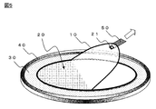
以下に先ダイシング法によりウエハを個片化した後のチップのピックアップについて、図面を参照して説明する。先ダイシングにより、半導体ウエハは個片化され、バックグラインドテープ10上には個片化された多数のチップ21からなるチップ群20が得られる(図1)。このチップ群20は、ピックアップテープ30と呼ばれる粘着テープに転写され、必要に応じてチップ間隔を拡張するエキスパンドを行った後に、ピックアップテープ30から剥離される(特許文献1:特開2012-209385号公報)。このピックアップテープ30としては、ダイシングテープと呼ばれる粘着テープ類が使用されることが多い。バックグラインドテープ10からピックアップテープ30へのチップ群20の転写は、以下のように行われる。すなわち、バックグラインドテープ10上の保持されたチップ群20にピックアップテープ30を貼付する。この際、ピックアップテープ30の外周部をリングフレーム40により固定する(図2)。次いでバックグラインドテープ10のみを剥離することで、チップ群20はピックアップテープ30に転写される。
Hereinafter, picking up a chip after the wafer is separated into pieces by the prior dicing method will be described with reference to the drawings. The semiconductor wafer is separated into pieces by the first dicing, and a chip group 20 composed of a large number of separated chips 21 is obtained on the back grind tape 10 (FIG. 1). This chip group 20 is transferred to an adhesive tape called a pickup tape 30 and is expanded from the pickup tape 30 after expanding to expand the chip interval as necessary (Patent Document 1: Japanese Patent Application Laid-Open No. 2012-209385). Publication). As this pickup tape 30, adhesive tapes called dicing tape are often used. The transfer of the chip group 20 from the back grind tape 10 to the pickup tape 30 is performed as follows. That is, the pickup tape 30 is attached to the chip group 20 held on the back grind tape 10. At this time, the outer peripheral portion of the pickup tape 30 is fixed by the ring frame 40 (FIG. 2). Next, the chip group 20 is transferred to the pickup tape 30 by peeling only the back grind tape 10.
バックグラインドテープ10は、裏面研削工程ではウエハやチップ群を安定して保持できる程度の粘着力が必要であり、チップ群をピックアップテープ30に転写する際にはチップ表面から容易に剥離できる程度の粘着力であることを要する。このため、バックグラインドテープ10の粘着剤層12には、エネルギー線照射により粘着力を低減できるエネルギー線硬化性粘着剤が使用されることが多い。たとえば特許文献2(特開2002-053819号公報)には、エネルギー線硬化前の粘着力が150g/25mm以上であり、エネルギー線硬化後の粘着力が150g/25mm以下となるバックグラインドテープが開示されている。ここで粘着力は、JIS Z-0237に規定される方法に準拠して、被着体としてSUS304-BA板を用い、剥離速度300mm/分、剥離角度180度の条件下で測定した粘着力である。
The back grind tape 10 needs an adhesive force that can stably hold the wafer and the chip group in the back grinding process, and can be easily peeled off from the chip surface when the chip group is transferred to the pickup tape 30. It must be adhesive. For this reason, in the adhesive layer 12 of the back grind tape 10, an energy ray-curable adhesive that can reduce the adhesive force by energy ray irradiation is often used. For example, Patent Document 2 (Japanese Patent Application Laid-Open No. 2002-053819) discloses a back grind tape in which the adhesive strength before energy beam curing is 150 g / 25 mm or more and the adhesive strength after energy beam curing is 150 g / 25 mm or less. Has been. Here, the adhesive strength is an adhesive strength measured using a SUS304-BA plate as an adherend and a peeling speed of 300 mm / min and a peeling angle of 180 degrees in accordance with the method defined in JIS Z-0237. is there.
また、特許文献3(特開2016-72546号公報)には、先ダイシング法に用いられる半導体ウエハ表面保護用粘着テープが開示されている。この粘着テープは、先ダイシング時におけるカーフシフトを抑制し、半導体チップへの粘着剤の転着、および半導体チップの剥離不良を解消することを目的とし、粘着テープの基材が、引張弾性率1~10GPaの剛性層を少なくとも1層有し、粘着剤層を放射線硬化させた後における剥離角度30°での剥離力が、0.1~3.0N/25mmであることを特定している。
Further, Patent Document 3 (Japanese Patent Laid-Open No. 2016-72546) discloses a semiconductor wafer surface protecting adhesive tape used in the prior dicing method. This pressure-sensitive adhesive tape is intended to suppress kerf shift at the time of dicing and eliminate the transfer of the pressure-sensitive adhesive to the semiconductor chip and the separation failure of the semiconductor chip. It has at least one rigid layer of ˜10 GPa, and it is specified that the peel force at a peel angle of 30 ° after radiation-curing the adhesive layer is 0.1 to 3.0 N / 25 mm.
バックグラインドテープ10の剥離時には、バックグラインドテープ10の背面(基材面)に剥離の切っ掛けとなる剥離用テープ50を固定する(図3)。バックグラインドテープは、半導体ウエハと略同形状であり、剥離の切っ掛けとなる起点がないため、短冊状の剥離用テープ50を固定して剥離の起点とする。剥離用テープ50は、バックグラインドテープ10背面に熱圧着によって強く固定される。
When the back grind tape 10 is peeled off, a peeling tape 50 as a starting point for peeling is fixed to the back surface (base material surface) of the back grind tape 10 (FIG. 3). Since the back grind tape has substantially the same shape as the semiconductor wafer and does not have a starting point for peeling, the strip-like peeling tape 50 is fixed as a starting point for peeling. The peeling tape 50 is strongly fixed to the back surface of the back grind tape 10 by thermocompression bonding.
バックグラインドテープ10に剥離用テープ50を熱圧着する際には、140~230℃程度に加熱し、圧力を加えて、バックグラインドテープ10背面に剥離用テープ50をヒートシールする。このため、ヒートシール部分に位置するバックグラインドテープの粘着剤層も加熱、加圧される。この結果、エネルギー線照射により硬化した粘着剤層が、加熱、加圧により流動、活性化し、バックグラインドテープの硬化後の粘着剤層と、チップとが熱圧着される。この状態で剥離用テープを起点としてバックグラインドテープ10の剥離を行うと、ヒートシール部およびその近傍で、チップ21がバックグラインドテープ10に固着された状態でバックグラインドテープが剥離し、チップの収率が低下する(図4、図5)。以下、この現象を「チップの転写不良」と呼ぶことがある。
When the peeling tape 50 is thermocompression bonded to the back grind tape 10, it is heated to about 140 to 230 ° C., pressure is applied, and the peeling tape 50 is heat sealed to the back of the back grind tape 10. For this reason, the adhesive layer of the back grind tape located in the heat seal portion is also heated and pressurized. As a result, the pressure-sensitive adhesive layer cured by irradiation with energy rays is flowed and activated by heating and pressurization, and the pressure-sensitive adhesive layer after curing of the back grind tape and the chip are thermocompression bonded. In this state, when the back grind tape 10 is peeled from the peeling tape as a starting point, the back grind tape is peeled off in a state where the chip 21 is fixed to the back grind tape 10 at and near the heat seal portion. The rate decreases (FIGS. 4 and 5). Hereinafter, this phenomenon may be referred to as “chip transfer failure”.
チップサイズが比較的大きな場合には、バックグラインドテープとチップ表面との剥離は良好に行われたが、チップサイズが小さくなるにつれて、チップがバックグラインドテープの粘着剤層12に埋め込まれ易くなる。この結果、バックグラインドテープからのチップの剥離がより困難になり、チップの転写不良が増大する。さらに、先ダイシング法では、バックグラインドテープの基材11として比較的硬質な基材が用いられることが多い。このため、バックグラインドテープの剥離時に、バックグラインドテープを十分に折り返すことができないことも剥離を困難にし、転写不良を増大する要因となる。
When the chip size is relatively large, the back grind tape and the chip surface were peeled off satisfactorily. However, as the chip size becomes smaller, the chip is easily embedded in the adhesive layer 12 of the back grind tape. As a result, peeling of the chip from the back grind tape becomes more difficult, and chip transfer failure increases. Furthermore, in the prior dicing method, a relatively hard substrate is often used as the substrate 11 of the back grind tape. For this reason, when the back grind tape is peeled off, the fact that the back grind tape cannot be sufficiently folded also makes peeling difficult and increases transfer defects.
特許文献3では、基材が硬質であるため、粘着テープを折り曲げることが困難になる。このため、剥離角度を鋭角となり、剥離力が強く、剥離に時間が掛かる。
In Patent Document 3, since the base material is hard, it is difficult to bend the adhesive tape. For this reason, the peeling angle becomes an acute angle, the peeling force is strong, and peeling takes time.
したがって、本発明は、特に先ダイシング法を採用した微小半導体チップの製造時に、チップ群20をバックグラインドテープ10から、ピックアップテープまたは接着テープのような他のテープに転写する際に、チップ21の転写不良を低減することを目的としている。また、バックグラインドテープからピックアップテープまたは接着テープのような他のテープへのチップの転写効率を改善することを目的としている。
Therefore, according to the present invention, the chip group 20 is transferred when the chip group 20 is transferred from the back grind tape 10 to another tape such as a pick-up tape or an adhesive tape, particularly when manufacturing a small semiconductor chip employing the tip dicing method. The object is to reduce transfer defects. Another object is to improve the transfer efficiency of chips from a back grind tape to another tape such as a pickup tape or an adhesive tape.
このような課題の解決を目的とした本発明の要旨は以下の通りである。
(1)基材と、その片面に設けられた粘着剤層とを含む粘着テープであって、
前記粘着剤層が、エネルギー線硬化性粘着剤からなり、
エネルギー線照射して硬化した後の粘着剤の200℃における貯蔵弾性率E’200が1.5MPa以上である粘着テープ。
(2)半導体ウエハ表面に溝が形成された半導体ウエハの表面にバックグラインドテープを貼付して、裏面を研削して、その研削により半導体ウエハを半導体チップに個片化し、その後個片化されたチップ群をピックアップテープまたは接着テープに転写する工程を含む半導体装置の製造方法において、前記バックグラインドテープとして使用される、(1)に記載の粘着テープ。
(3)半導体ウエハ表面に溝が形成された半導体ウエハの表面にバックグラインドテープを貼付して、裏面を研削して、その研削により半導体ウエハを半導体チップに個片化し、その後個片化されたチップ群をピックアップテープまたは接着テープに転写する工程を含む半導体装置の製造方法において、前記バックグラインドテープとして(1)に記載の粘着テープを使用する半導体装置の製造方法。
(4)上記(1)に記載の粘着テープの使用であって、半導体ウエハ表面に溝が形成された半導体ウエハの表面にバックグラインドテープを貼付して、裏面を研削して、その研削により半導体ウエハを半導体チップに個片化し、その後個片化されたチップ群をピックアップテープまたは接着テープに転写する工程を含む半導体装置の製造方法における、前記バックグラインドテープとしての使用。 The gist of the present invention aimed at solving such problems is as follows.
(1) A pressure-sensitive adhesive tape comprising a base material and a pressure-sensitive adhesive layer provided on one side thereof,
The pressure-sensitive adhesive layer is made of an energy ray-curable pressure-sensitive adhesive,
The adhesive tape whose storage elastic modulus E'200 in 200 degreeC of the adhesive after hardening by energy ray irradiation is 1.5 Mpa or more.
(2) A back grind tape was applied to the surface of the semiconductor wafer having grooves formed on the surface of the semiconductor wafer, the back surface was ground, and the semiconductor wafer was separated into semiconductor chips by the grinding, and then separated into pieces. The pressure-sensitive adhesive tape according to (1), which is used as the back grind tape in a semiconductor device manufacturing method including a step of transferring a chip group to a pickup tape or an adhesive tape.
(3) A back grind tape was applied to the surface of the semiconductor wafer having grooves formed on the surface of the semiconductor wafer, the back surface was ground, and the semiconductor wafer was separated into semiconductor chips by the grinding, and then separated into pieces. In the manufacturing method of the semiconductor device including the process of transferring a chip group to a pick-up tape or an adhesive tape, the manufacturing method of the semiconductor device which uses the adhesive tape as described in (1) as said back grind tape.
(4) Use of the adhesive tape as described in (1) above, wherein a back grind tape is applied to the surface of the semiconductor wafer having grooves formed on the surface of the semiconductor wafer, the back surface is ground, and the semiconductor is ground by the grinding. Use as the back grind tape in a method of manufacturing a semiconductor device including a step of separating a wafer into semiconductor chips and then transferring the separated chips to a pickup tape or an adhesive tape.
本発明に係る粘着テープ10によれば、エネルギー線硬化性粘着剤層の硬化後に、剥離用テープ50の熱圧着を行なっても、被着体(半導体チップ)と粘着テープとの粘着力を極めて低いレベルに抑えられ、チップの転写不良を防止できる。
According to the pressure-sensitive adhesive tape 10 according to the present invention, the adhesive force between the adherend (semiconductor chip) and the pressure-sensitive adhesive tape is extremely high even when the peeling tape 50 is subjected to thermocompression bonding after the energy ray-curable pressure-sensitive adhesive layer is cured. It is suppressed to a low level, and chip transfer failure can be prevented.
以下、本発明に係る粘着テープについて、具体的に説明する。まず、本明細書で使用する主な用語を説明する。
本明細書において、例えば「(メタ)アクリレート」とは、「アクリレート」及び「メタクリレート」の双方を示す語として用いており、他の類似用語についても同様である。 Hereinafter, the adhesive tape according to the present invention will be specifically described. First, main terms used in this specification will be described.
In this specification, for example, “(meth) acrylate” is used as a term indicating both “acrylate” and “methacrylate”, and the same applies to other similar terms.
粘着テープとは、基材と、その片面に設けられた粘着剤層とを含む積層体を意味し、これら以外の他の構成層を含むことを妨げない。たとえば、粘着剤層側の基材表面にはプライマー層(易接着層)が形成されていてもよく、粘着剤層の表面には、使用時まで粘着剤層を保護するための剥離シートが積層されていてもよい。また、基材は単層であってもよく、緩衝層などの機能層を備えた多層であってもよい。粘着剤層も同様である。
半導体ウエハの「表面」とは回路が形成された面を指し、「裏面」は回路が形成されていない面を指す。
半導体ウエハの個片化とは、半導体ウエハを回路毎に分割し、半導体チップを得ることを言う。 An adhesive tape means the laminated body containing a base material and the adhesive layer provided in the single side | surface, and does not prevent including other structural layers other than these. For example, a primer layer (easily adhesive layer) may be formed on the surface of the base material on the side of the pressure-sensitive adhesive layer, and a release sheet for protecting the pressure-sensitive adhesive layer is laminated on the surface of the pressure-sensitive adhesive layer until use. May be. Further, the substrate may be a single layer or a multilayer having a functional layer such as a buffer layer. The same applies to the pressure-sensitive adhesive layer.
The “front surface” of the semiconductor wafer refers to the surface on which the circuit is formed, and the “back surface” refers to the surface on which the circuit is not formed.
Dividing the semiconductor wafer into pieces means dividing the semiconductor wafer into circuits to obtain semiconductor chips.
シリコンベアウエハとは、パターン形成などの加工処理を行う前の状態のシリコンウエハであり、表面は鏡面研磨されている。
先ダイシング法とは、ウエハの表面側から所定深さの溝を形成した後、ウエハ裏面側から研削を行い、研削によりウエハを個片化する方法を言う。 A silicon bare wafer is a silicon wafer in a state before processing such as pattern formation, and its surface is mirror-polished.
The pre-dicing method refers to a method in which after a groove having a predetermined depth is formed from the front surface side of the wafer, grinding is performed from the back surface side of the wafer, and the wafer is separated into pieces by grinding.
バックグラインドテープとは、半導体ウエハの裏面研削時にウエハ回路面を保護するために使用される粘着テープであり、特に本明細書では先ダイシング法に好ましく使用される粘着テープを指す。
ピックアップテープとは、チップ群を転写し、チップのピックアップを行うための粘着テープであり、典型的にはダイシングテープと呼ばれる粘着テープ類が用いられる。
接着テープとは、接着剤として機能する薄層を有し、接着剤層を他の被着体に転写するために用いられる各種のテープを意味する。具体的には、フィルム状接着剤と剥離シートとの積層体、ダイシングテープとフィルム状接着剤との積層体や、ダイシングテープとダイボンディングテープの両方の機能を有する接着剤層と剥離シートとからなるダイシング・ダイボンディングテープ等が挙げられる。 The back grind tape is an adhesive tape that is used to protect the wafer circuit surface during grinding of the back surface of a semiconductor wafer, and particularly refers to an adhesive tape that is preferably used in the prior dicing method in this specification.
The pickup tape is an adhesive tape for transferring a chip group and picking up a chip. Typically, an adhesive tape called a dicing tape is used.
The adhesive tape means various tapes that have a thin layer that functions as an adhesive and are used for transferring the adhesive layer to another adherend. Specifically, from a laminate of a film adhesive and a release sheet, a laminate of a dicing tape and a film adhesive, and an adhesive layer and a release sheet having the functions of both a dicing tape and a die bonding tape The dicing die-bonding tape etc. which become.
本発明に係る粘着テープは、上記バックグラインドテープとして特に好ましく用いられる。本発明に係る粘着テープ10は、基材11と、その片面に設けられた粘着剤層12とを含む。以下に、本発明の粘着テープ10の各部材の構成をさらに詳細に説明する。
[基材11]
粘着テープ10の基材11には、バックグラインドテープの基材として使用されている各種の樹脂フィルムが用いられる。 The pressure-sensitive adhesive tape according to the present invention is particularly preferably used as the back grind tape. The pressure-sensitive adhesive tape 10 according to the present invention includes a base material 11 and a pressure-sensitive adhesive layer 12 provided on one surface thereof. Below, the structure of each member of the adhesive tape 10 of this invention is demonstrated in detail.
[Substrate 11]
As the base material 11 of the pressure-sensitive adhesive tape 10, various resin films used as the base material of the back grind tape are used.
[基材11]
粘着テープ10の基材11には、バックグラインドテープの基材として使用されている各種の樹脂フィルムが用いられる。 The pressure-sensitive adhesive tape according to the present invention is particularly preferably used as the back grind tape. The pressure-
[Substrate 11]
As the base material 11 of the pressure-
以下に本発明で用いられる基材11の一例を詳述するが、これらは単に基材の入手を容易するための記載であって、何ら限定的に解釈されるべきではない。
Hereinafter, although an example of the base material 11 used in the present invention will be described in detail, these are merely descriptions for facilitating the acquisition of the base material and should not be construed as limiting in any way.
本発明の基材は、たとえば比較的硬質の樹脂フィルムであってもよい。また、基材の片面もしくは両面には、比較的軟質の樹脂フィルムからなる緩衝層が積層されていてもよい。
The substrate of the present invention may be a relatively hard resin film, for example. Moreover, the buffer layer which consists of a comparatively soft resin film may be laminated | stacked on the single side | surface or both surfaces of a base material.
好ましい基材は、ヤング率が1000MPa以上である。ヤング率が1000MPa未満の基材を使用すると、粘着テープによる半導体ウエハ又は半導体チップに対する保持性能が低下し、裏面研削時の振動等を抑制することができず、半導体チップの欠けや破損が発生しやすくなる。一方、基材のヤング率を1000MPa以上とすることで、粘着テープによる半導体ウエハ又は半導体チップに対する保持性能が高まり、裏面研削時の振動等を抑制し、半導体チップの欠けや破損を防止できる。また、粘着テープを半導体チップから剥離する際の応力を小さくすることが可能になり、テープ剥離時に生じるチップの欠けや破損を防止できる。さらに、粘着テープを半導体ウエハに貼付する際の作業性も良好にすることが可能である。このような観点から、基材のヤング率は、好ましくは1800~30000MPa、より好ましくは2500~6000MPaである。
A preferable base material has a Young's modulus of 1000 MPa or more. If a base material with a Young's modulus of less than 1000 MPa is used, the holding performance of the adhesive tape on the semiconductor wafer or semiconductor chip will be reduced, vibrations during back grinding cannot be suppressed, and chipping or breakage of the semiconductor chip will occur. It becomes easy. On the other hand, when the Young's modulus of the base material is set to 1000 MPa or more, the holding performance of the adhesive tape on the semiconductor wafer or the semiconductor chip is enhanced, vibration during back surface grinding, etc. can be suppressed, and chipping or breakage of the semiconductor chip can be prevented. Moreover, it becomes possible to reduce the stress at the time of peeling off the adhesive tape from the semiconductor chip, and chipping or breakage of the chip that occurs at the time of tape peeling can be prevented. Furthermore, it is possible to improve the workability when attaching the adhesive tape to the semiconductor wafer. From such a viewpoint, the Young's modulus of the base material is preferably 1800 to 30000 MPa, more preferably 2500 to 6000 MPa.
基材11の厚さ(D1)は特に限定されないが、500μm以下であることが好ましく、15~350μmであることがより好ましく、20~160μmであることがさらに好ましい。基材の厚さを500μm以下とすることで、粘着テープの剥離力を制御しやすくなる。また、15μm以上とすることで、基材が粘着テープの支持体としての機能を果たしやすくなる。
The thickness (D1) of the substrate 11 is not particularly limited, but is preferably 500 μm or less, more preferably 15 to 350 μm, and further preferably 20 to 160 μm. By making the thickness of the base material 500 μm or less, it becomes easy to control the peeling force of the adhesive tape. Moreover, by setting it as 15 micrometers or more, it becomes easy for a base material to fulfill | perform the function as a support body of an adhesive tape.
基材11の材質としては、種々の樹脂フィルムを用いることができる。ここで、ヤング率が1000MPa以上の基材として、たとえばポリエチレンテレフタレート、ポリエチレンナフタレート、ポリブチレンテレフタレート、全芳香族ポリエステル等のポリエステル、ポリイミド、ポリアミド、ポリカーボネート、ポリアセタール、変性ポリフェニレンオキシド、ポリフェニレンスルフィド、ポリスルホン、ポリエーテルケトン、二軸延伸ポリプロピレン等の樹脂フィルムが挙げられる。
これら樹脂フィルムの中でも、ポリエステルフィルム、ポリアミドフィルム、ポリイミドフィルム、二軸延伸ポリプロピレンフィルムから選ばれる1種以上を含むフィルムが好ましく、ポリエステルフィルムを含むことがより好ましく、ポリエチレンテレフタレートフィルムを含むことがさらに好ましい。 As a material of the base material 11, various resin films can be used. Here, as a substrate having a Young's modulus of 1000 MPa or more, for example, polyethylene terephthalate, polyethylene naphthalate, polybutylene terephthalate, polyester such as wholly aromatic polyester, polyimide, polyamide, polycarbonate, polyacetal, modified polyphenylene oxide, polyphenylene sulfide, polysulfone, Examples of the resin film include polyether ketone and biaxially stretched polypropylene.
Among these resin films, a film containing at least one selected from a polyester film, a polyamide film, a polyimide film, and a biaxially stretched polypropylene film is preferable, a polyester film is more preferable, and a polyethylene terephthalate film is further preferable. .
また、基材には、本発明の効果を損なわない範囲において、可塑剤、滑剤、赤外線吸収剤、紫外線吸収剤、フィラー、着色剤、帯電防止剤、酸化防止剤、触媒等を含有させてもよい。また、基材は、粘着剤層を硬化する際に照射されるエネルギー線に対して透過性を有する。
また、基材の少なくとも一方の表面には、緩衝層及び粘着剤層の少なくとも一方との密着性を向上させるために、コロナ処理等の接着処理を施してもよい。また、基材は、上記した樹脂フィルムと、樹脂フィルムの少なくとも一方の表面に被膜された易接着層(プライマー層)とを有しているものでもよい。 In addition, the base material may contain a plasticizer, a lubricant, an infrared absorber, an ultraviolet absorber, a filler, a colorant, an antistatic agent, an antioxidant, a catalyst and the like as long as the effects of the present invention are not impaired. Good. Moreover, a base material has permeability | transmittance with respect to the energy ray irradiated when hardening an adhesive layer.
Further, at least one surface of the substrate may be subjected to an adhesion treatment such as a corona treatment in order to improve adhesion with at least one of the buffer layer and the pressure-sensitive adhesive layer. Moreover, the base material may have the above-described resin film and an easy adhesion layer (primer layer) coated on at least one surface of the resin film.
易接着層を形成する易接着層形成用組成物としては、特に限定されないが、例えば、ポリエステル系樹脂、ウレタン系樹脂、ポリエステルウレタン系樹脂、アクリル系樹脂等を含む組成物が挙げられる。易接着層形成用組成物には、必要に応じて、架橋剤、光重合開始剤、酸化防止剤、軟化剤(可塑剤)、充填剤、防錆剤、顔料、染料等を含有してもよい。
易接着層の厚さとしては、好ましくは0.01~10μm、より好ましくは0.03~5μmである。なお、易接着層の厚さは、基材の厚さに対して小さく、材質も柔らかいため、ヤング率に与える影響は小さく、基材のヤング率は、易接着層を有する場合でも、樹脂フィルムのヤング率と実質的に同一である。 Although it does not specifically limit as a composition for easy-adhesion layer formation which forms an easy-adhesion layer, For example, the composition containing a polyester-type resin, a urethane-type resin, a polyester urethane-type resin, an acrylic resin etc. is mentioned. The easy-adhesion layer forming composition may contain a crosslinking agent, a photopolymerization initiator, an antioxidant, a softening agent (plasticizer), a filler, an antirust agent, a pigment, a dye, and the like, if necessary. Good.
The thickness of the easy adhesion layer is preferably 0.01 to 10 μm, more preferably 0.03 to 5 μm. In addition, since the thickness of the easy adhesion layer is smaller than the thickness of the base material and the material is soft, the influence on the Young's modulus is small. The Young's modulus of the base material is a resin film even when the easy adhesion layer is provided. Is substantially the same as the Young's modulus.
[緩衝層]
上記基材11の片面もしくは両面には、緩衝層が設けられていても良い。緩衝層は、比較的軟質の樹脂フィルムからなり、半導体ウエハの研削による振動を緩和して、半導体ウエハに割れ及び欠けが生じることを防止する。また、粘着テープを貼付した半導体ウエハは、裏面研削時に、吸着テーブル上に配置されるが、粘着テープは緩衝層を設けたことで、吸着テーブルに適切に保持されやすくなる。 [Buffer layer]
A buffer layer may be provided on one side or both sides of the substrate 11. The buffer layer is made of a relatively soft resin film, and relieves vibration caused by grinding of the semiconductor wafer to prevent the semiconductor wafer from being cracked or chipped. Further, the semiconductor wafer to which the adhesive tape is attached is arranged on the suction table at the time of back surface grinding, but the adhesive tape is easily held on the suction table by providing a buffer layer.
緩衝層の厚さ(D2)は、8~80μmであることが好ましく、10~60μmであることがさらに好ましい。
The thickness (D2) of the buffer layer is preferably 8 to 80 μm, and more preferably 10 to 60 μm.
緩衝層は、ポリプロピレンフィルム、エチレン-酢酸ビニル共重合体フィルム、アイオノマー樹脂フィルム、エチレン・(メタ)アクリル酸共重合体フィルム、エチレン・(メタ)アクリル酸エステル共重合体フィルム、LDPEフィルム、LLDPEフィルムが好ましい。また、エネルギー線重合性化合物を含む緩衝層形成用組成物から形成される層であってもよい。緩衝層を有する基材は、基材と緩衝層とをラミネートして得られる。
Buffer layer: polypropylene film, ethylene-vinyl acetate copolymer film, ionomer resin film, ethylene / (meth) acrylic acid copolymer film, ethylene / (meth) acrylic acid ester copolymer film, LDPE film, LLDPE film Is preferred. Moreover, the layer formed from the composition for buffer layer formation containing an energy-beam polymeric compound may be sufficient. The base material having the buffer layer is obtained by laminating the base material and the buffer layer.
[粘着剤層12]
粘着剤層12は、上記基材11の一方の面に直接または緩衝層を介して形成されている。本発明では、粘着剤層がエネルギー線硬化性粘着剤からなり、硬化後の粘着剤の200℃における貯蔵弾性率E’200が1.5MPa以上であることを特徴としている。
以下、粘着剤の硬化後の200℃における貯蔵弾性率を、硬化後貯蔵弾性率とよぶことがある。 [Adhesive layer 12]
The pressure-sensitive adhesive layer 12 is formed on one surface of the substrate 11 directly or via a buffer layer. In the present invention, the pressure-sensitive adhesive layer is made of an energy ray-curable pressure-sensitive adhesive, and the storage elastic modulus E ′ 200 at 200 ° C. of the pressure-sensitive adhesive after curing is 1.5 MPa or more.
Hereinafter, the storage elastic modulus at 200 ° C. after curing of the pressure-sensitive adhesive may be referred to as post-curing storage elastic modulus.
粘着剤層12は、上記基材11の一方の面に直接または緩衝層を介して形成されている。本発明では、粘着剤層がエネルギー線硬化性粘着剤からなり、硬化後の粘着剤の200℃における貯蔵弾性率E’200が1.5MPa以上であることを特徴としている。
以下、粘着剤の硬化後の200℃における貯蔵弾性率を、硬化後貯蔵弾性率とよぶことがある。 [Adhesive layer 12]
The pressure-
Hereinafter, the storage elastic modulus at 200 ° C. after curing of the pressure-sensitive adhesive may be referred to as post-curing storage elastic modulus.
硬化後貯蔵弾性率は、粘着剤の組成によって制御できる。硬化後貯蔵弾性率を制御するための一般的な指針については後述する。
エネルギー線照射して硬化した後の粘着剤の200℃における貯蔵弾性率E’200は、好ましくは2.0~100MPa、さらに好ましくは2.5~70MPaの範囲にある。硬化後貯蔵弾性率E’200が上記範囲にあることで、粘着剤層の硬化後であってもチップ群20を安定して保持することができ、かつピックアップテープ30または接着テープへのチップ群の転写時には、粘着剤層をチップ群から容易に残渣物を残すことなく剥離できる。硬化後貯蔵弾性率を測定する際には、粘着剤をエネルギー線照射により完全に硬化する。すなわち、さらにエネルギー線照射を行っても、弾性率の変化が起らない程度にまで硬化する。 The storage elastic modulus after curing can be controlled by the composition of the pressure-sensitive adhesive. General guidelines for controlling the storage modulus after curing will be described later.
The storage elastic modulus E ′ 200 at 200 ° C. of the pressure-sensitive adhesive after being cured by irradiation with energy rays is preferably 2.0 to 100 MPa, more preferably 2.5 to 70 MPa. Since the post-curing storage elastic modulus E ′ 200 is in the above range, thechip group 20 can be stably held even after the pressure-sensitive adhesive layer is cured, and the chip group to the pickup tape 30 or the adhesive tape can be retained. During the transfer, the pressure-sensitive adhesive layer can be easily peeled from the chip group without leaving a residue. When measuring the storage elastic modulus after curing, the pressure-sensitive adhesive is completely cured by irradiation with energy rays. That is, even when energy beam irradiation is further performed, the resin is cured to such an extent that the elastic modulus does not change.
エネルギー線照射して硬化した後の粘着剤の200℃における貯蔵弾性率E’200は、好ましくは2.0~100MPa、さらに好ましくは2.5~70MPaの範囲にある。硬化後貯蔵弾性率E’200が上記範囲にあることで、粘着剤層の硬化後であってもチップ群20を安定して保持することができ、かつピックアップテープ30または接着テープへのチップ群の転写時には、粘着剤層をチップ群から容易に残渣物を残すことなく剥離できる。硬化後貯蔵弾性率を測定する際には、粘着剤をエネルギー線照射により完全に硬化する。すなわち、さらにエネルギー線照射を行っても、弾性率の変化が起らない程度にまで硬化する。 The storage elastic modulus after curing can be controlled by the composition of the pressure-sensitive adhesive. General guidelines for controlling the storage modulus after curing will be described later.
The storage elastic modulus E ′ 200 at 200 ° C. of the pressure-sensitive adhesive after being cured by irradiation with energy rays is preferably 2.0 to 100 MPa, more preferably 2.5 to 70 MPa. Since the post-curing storage elastic modulus E ′ 200 is in the above range, the
また、一般的に硬化後の粘着剤は、常温では比較的貯蔵弾性率が高く、高温になるにつれて貯蔵弾性率が低下する傾向にある。しかし、本発明の粘着剤は、高温においても高い硬化後貯蔵弾性率を維持する。
In general, the cured adhesive has a relatively high storage elastic modulus at room temperature, and the storage elastic modulus tends to decrease as the temperature increases. However, the pressure-sensitive adhesive of the present invention maintains a high post-curing storage modulus even at high temperatures.
したがって、剥離用テープ50を熱圧着する際の条件が高温であっても、本発明の粘着テープによれば、硬化後の粘着剤層が軟化し難い。この結果、剥離用テープを高温で熱圧着しても、チップの転写不良を大幅に低減できる。
Therefore, even if the conditions for thermocompression bonding of the peeling tape 50 are high, according to the adhesive tape of the present invention, the cured adhesive layer is difficult to soften. As a result, even if the peeling tape is thermocompression bonded at a high temperature, transfer defects of the chip can be greatly reduced.
また粘着剤のエネルギー線硬化前の23℃における貯蔵弾性率は、0.05~0.50MPaであることが好ましい。さらに、エネルギー線硬化前の23℃における損失正接(tanδ=損失弾性率/貯蔵弾性率)は、好ましくは0.2以上である。半導体ウエハの表面には、回路等が形成され通常凹凸がある。粘着テープは、粘着剤の貯蔵弾性率およびtanδが上記範囲内にあることで、凹凸があるウエハ表面に貼付される際、ウエハ表面の凹凸と粘着剤層とを十分に接触させ、かつ粘着剤層の接着性を適切に発揮させることが可能になる。そのため、粘着テープの半導体ウエハへの固定を確実に行い、かつ裏面研削時にウエハ表面を適切に保護することが可能になる。これらの観点から、粘着剤のエネルギー線硬化前の23℃における貯蔵弾性率は、0.10~0.35MPaであることがより好ましい。
Further, the storage elastic modulus at 23 ° C. before the energy ray curing of the pressure-sensitive adhesive is preferably 0.05 to 0.50 MPa. Furthermore, the loss tangent at 23 ° C. (tan δ = loss elastic modulus / storage elastic modulus) before energy beam curing is preferably 0.2 or more. A circuit or the like is formed on the surface of the semiconductor wafer and is usually uneven. The pressure-sensitive adhesive tape has the storage elastic modulus and tan δ of the pressure-sensitive adhesive within the above ranges, so that when the wafer is affixed to a surface with irregularities, the wafer surface is sufficiently brought into contact with the pressure-sensitive adhesive layer, and the pressure-sensitive adhesive It becomes possible to appropriately exhibit the adhesiveness of the layer. Therefore, it becomes possible to securely fix the adhesive tape to the semiconductor wafer and to appropriately protect the wafer surface during back grinding. From these viewpoints, the storage elastic modulus at 23 ° C. before the energy ray curing of the adhesive is more preferably 0.10 to 0.35 MPa.
硬化後貯蔵弾性率E’200が、上記範囲にあることで、剥離用テープ50を高温で熱圧着しても、チップ等が粘着剤層に埋め込まれず、チップの転写不良を大幅に低減できる。たとえば粘着テープ10の粘着剤層12をシリコンウエハ鏡面に貼付後、粘着剤層にエネルギー線照射して硬化し、さらに圧力0.5N/cm2、210℃で5秒間熱圧着した後の23℃における、シリコンウエハ鏡面と粘着剤層との間の粘着力(以下、「熱圧着後粘着力」と呼ぶ)は、好ましくは9.0N/25mm以下であり、さらに好ましくは0.001~7N/25mm、さらに好ましくは0.1~1N/25mmの範囲にある。また粘着剤層は、エネルギー線硬化前には常温において適度な感圧接着性を有する。エネルギー線硬化前の粘着剤層のシリコンウエハ鏡面に対する23℃での粘着力は、好ましくは10~1500mN/25mm、さらに好ましくは10~700mN/25mmの範囲にある。
When the post-cure storage elastic modulus E ′ 200 is in the above range, even if the peeling tape 50 is thermocompression bonded at a high temperature, the chip or the like is not embedded in the adhesive layer, and the transfer failure of the chip can be greatly reduced. For example, after the pressure-sensitive adhesive layer 12 of the pressure-sensitive adhesive tape 10 is applied to a mirror surface of a silicon wafer, the pressure-sensitive adhesive layer is cured by irradiation with energy rays, and further subjected to thermocompression bonding at a pressure of 0.5 N / cm 2 and 210 ° C. for 5 seconds. The adhesive strength between the mirror surface of the silicon wafer and the adhesive layer (hereinafter referred to as “adhesive strength after thermocompression bonding”) is preferably 9.0 N / 25 mm or less, more preferably 0.001 to 7 N / It is in the range of 25 mm, more preferably 0.1 to 1 N / 25 mm. Further, the pressure-sensitive adhesive layer has an appropriate pressure-sensitive adhesive property at room temperature before energy ray curing. The pressure-sensitive adhesive force at 23 ° C. of the pressure-sensitive adhesive layer before energy ray curing on the silicon wafer mirror surface is preferably in the range of 10 to 1500 mN / 25 mm, more preferably 10 to 700 mN / 25 mm.
熱圧着後粘着力を測定する際には、粘着剤層をエネルギー線照射により完全に硬化する。すなわち、さらにエネルギー線照射を行っても、粘着力の低下が起らない程度にまで硬化する。熱圧着は、熱プレス機などにより行う。この際、粘着テープの基材側表面には、後に説明する剥離用テープ50を同時に熱圧着する。剥離用テープ50は剥離の起点となり、また測定装置の係合にも使用される。なお、後述の熱圧着後粘着力の測定では、剥離の進行に伴い、測定される粘着力が変動することがある。本発明では、粘着テープ10の剥離が完了するまでの最大値を熱圧着後粘着力と呼ぶ。
When measuring the adhesive strength after thermocompression bonding, the adhesive layer is completely cured by irradiation with energy rays. That is, even if energy ray irradiation is further performed, it is cured to such an extent that the adhesive force does not decrease. Thermocompression bonding is performed by a hot press machine or the like. At this time, a peeling tape 50, which will be described later, is thermocompression bonded simultaneously to the substrate side surface of the adhesive tape. The peeling tape 50 is a starting point of peeling and is also used for engagement of a measuring device. In the measurement of the adhesive strength after thermocompression bonding described later, the measured adhesive strength may vary with the progress of peeling. In this invention, the maximum value until peeling of the adhesive tape 10 is completed is called adhesive force after thermocompression bonding.
粘着剤層12の厚さ(D3)は、200μm未満であることが好ましく、5~55μmがより好ましく、10~50μmがさらに好ましい。粘着剤層をこのように薄くすると、粘着テープにおいて、剛性の低い部分の割合を少なくすることができるため、裏面研削時に生じる半導体チップの欠けを一層防止しやすくなる。
The thickness (D3) of the pressure-sensitive adhesive layer 12 is preferably less than 200 μm, more preferably 5 to 55 μm, and even more preferably 10 to 50 μm. When the pressure-sensitive adhesive layer is thinned in this way, the ratio of the low-rigidity portion of the pressure-sensitive adhesive tape can be reduced, so that it becomes easier to prevent chipping of the semiconductor chip that occurs during back surface grinding.
粘着剤層12は、例えば、アクリル系粘着剤、ウレタン系粘着剤、ゴム系粘着剤、シリコーン系粘着剤等を主剤とするエネルギー線硬化性粘着剤から形成されるが、アクリル系のエネルギー線硬化性粘着剤が好ましい。
The pressure-sensitive adhesive layer 12 is formed of, for example, an energy ray-curable pressure-sensitive adhesive mainly composed of an acrylic pressure-sensitive adhesive, a urethane-based pressure-sensitive adhesive, a rubber-based pressure-sensitive adhesive, or a silicone-based pressure-sensitive adhesive. An adhesive is preferred.
粘着剤層12は、エネルギー線硬化性粘着剤から形成されることで、エネルギー線照射による硬化前には、23℃における粘着力、弾性率を上記範囲に設定しつつ、硬化後においては粘着力を1000mN/50mm以下に容易に設定することが可能になる。なお、ここで粘着力とは、後述するヒートシール部を除く部分の粘着テープの粘着力をいう。
The pressure-sensitive adhesive layer 12 is formed of an energy ray-curable pressure-sensitive adhesive, so that the pressure-sensitive adhesive force and the elastic modulus at 23 ° C. are set within the above ranges before being cured by irradiation with energy rays, and the pressure-sensitive adhesive strength is obtained after curing. Can be easily set to 1000 mN / 50 mm or less. In addition, adhesive force means the adhesive force of the adhesive tape of the part except the heat seal part mentioned later here.
また、粘着剤層12は、エネルギー線硬化後の状態における破断応力が、好ましくは10MPa以上であり、特に好ましくは15MPa以上である。また、エネルギー線硬化後の破断伸度が、好ましくは15%以上であり、特に好ましくは20%以上である。このように、破断応力の値が10MPa以上であり、破断伸度の値が15%以上である場合、エネルギー線硬化性粘着剤層の引張り物性は良好であり、たとえ紫外線等の照射が不十分であり、エネルギー線硬化性粘着剤層が十分に硬化されなかった場合においても、ウエハ上に粘着剤残渣が付着することを防止可能である。
Moreover, the adhesive layer 12 preferably has a breaking stress in a state after energy beam curing of 10 MPa or more, particularly preferably 15 MPa or more. Further, the elongation at break after energy beam curing is preferably 15% or more, and particularly preferably 20% or more. As described above, when the value of the breaking stress is 10 MPa or more and the value of the breaking elongation is 15% or more, the tensile physical properties of the energy ray-curable pressure-sensitive adhesive layer are good, and irradiation with ultraviolet rays or the like is insufficient. Even when the energy ray-curable pressure-sensitive adhesive layer is not sufficiently cured, it is possible to prevent the pressure-sensitive adhesive residue from adhering to the wafer.
以下、粘着剤の具体例について詳述するが、これらは非限定的例示であり、本発明における粘着剤層はこれらに限定的に解釈されるべきではない。
エネルギー線硬化性粘着剤としては、例えば、非エネルギー線硬化性の粘着性樹脂(「粘着性樹脂I」ともいう)に加え、粘着性樹脂以外のエネルギー線硬化性化合物を含むエネルギー線硬化性粘着剤組成物(以下、「X型の粘着剤組成物」ともいう)が使用可能である。また、エネルギー線硬化性粘着剤として、非エネルギー線硬化性の粘着性樹脂の側鎖に不飽和基を導入したエネルギー線硬化性の粘着性樹脂(以下、「粘着性樹脂II」ともいう)を主成分として含み、粘着性樹脂以外のエネルギー線硬化性化合物を含まない粘着剤組成物(以下、「Y型の粘着剤組成物」ともいう)も使用してもよい。 Hereinafter, although the specific example of an adhesive is explained in full detail, these are non-limiting illustrations, The adhesive layer in this invention should not be limitedly limited to these.
Examples of the energy ray curable adhesive include an energy ray curable adhesive containing an energy ray curable compound other than an adhesive resin in addition to a non-energy ray curable adhesive resin (also referred to as “adhesive resin I”). An agent composition (hereinafter also referred to as “X-type pressure-sensitive adhesive composition”) can be used. In addition, as an energy ray curable adhesive, an energy ray curable adhesive resin having an unsaturated group introduced into the side chain of a non-energy ray curable adhesive resin (hereinafter also referred to as “adhesive resin II”). An adhesive composition that is contained as a main component and does not contain an energy ray curable compound other than an adhesive resin (hereinafter also referred to as “Y-type adhesive composition”) may be used.
さらに、エネルギー線硬化性粘着剤としては、X型とY型の併用型、すなわち、エネルギー線硬化性の粘着性樹脂IIに加え、粘着性樹脂以外のエネルギー線硬化性化合物も含むエネルギー線硬化性粘着剤組成物(以下、「XY型の粘着剤組成物」ともいう)を使用してもよい。
これらの中では、XY型の粘着剤組成物を使用することが好ましい。XY型のものを使用することで、硬化前においては十分な粘着特性を有する一方で、硬化後においては、半導体ウエハに対する粘着力を十分に低くすることが可能である。 Furthermore, as the energy ray curable pressure sensitive adhesive, an X ray and Y type combined type, that is, an energy ray curable compound containing an energy ray curable compound other than the adhesive resin in addition to the energy ray curable adhesive resin II. An adhesive composition (hereinafter, also referred to as “XY-type adhesive composition”) may be used.
Among these, it is preferable to use an XY type pressure-sensitive adhesive composition. By using the XY type, the adhesive strength to the semiconductor wafer can be sufficiently lowered after curing, while having sufficient adhesive properties before curing.
なお、以下の説明において“粘着性樹脂”は、上記した粘着性樹脂I及び粘着性樹脂IIの一方又は両方を指す用語として使用する。具体的な粘着性樹脂としては、例えば、アクリル系樹脂、ウレタン系樹脂、ゴム系樹脂、シリコーン系樹脂等が挙げられるが、アクリル系樹脂が好ましい。
以下、粘着性樹脂として、アクリル系樹脂が使用されるアクリル系粘着剤についてより詳述に説明する。 In the following description, “adhesive resin” is used as a term indicating one or both of the above-described adhesive resin I and adhesive resin II. Specific examples of the adhesive resin include acrylic resins, urethane resins, rubber resins, and silicone resins. Acrylic resins are preferable.
Hereinafter, the acrylic adhesive in which an acrylic resin is used as the adhesive resin will be described in more detail.
アクリル系樹脂には、アクリル系重合体(b)が使用される。アクリル系重合体(b)は、少なくともアルキル(メタ)アクリレートを含むモノマーを重合して得たものであり、アルキル(メタ)アクリレート由来の構成単位を含む。アルキル(メタ)アクリレートとしては、アルキル基の炭素数が1~20のものが挙げられ、アルキル基は直鎖であってもよいし、分岐であってもよい。アルキル(メタ)アクリレートの具体例としては、メチル(メタ)アクリレート、エチル(メタ)アクリレート、イソプロピル(メタ)アクリレート、n-プロピル(メタ)アクリレート、n-ブチル(メタ)メタクリレート、2-エチルヘキシル(メタ)アクリレート、n-オクチル(メタ)アクリレート、イソオクチル(メタ)アクリレート、ノニル(メタ)アクリレート、デシル(メタ)アクリレート、ウンデシル(メタ)アクリレート、ドデシル(メタ)アクリレート等が挙げられる。アルキル(メタ)アクリレートは、単独で又は2種以上組み合わせて用いてもよい。
An acrylic polymer (b) is used for the acrylic resin. The acrylic polymer (b) is obtained by polymerizing a monomer containing at least an alkyl (meth) acrylate, and includes a structural unit derived from an alkyl (meth) acrylate. Examples of the alkyl (meth) acrylate include those having 1 to 20 carbon atoms in the alkyl group, and the alkyl group may be linear or branched. Specific examples of the alkyl (meth) acrylate include methyl (meth) acrylate, ethyl (meth) acrylate, isopropyl (meth) acrylate, n-propyl (meth) acrylate, n-butyl (meth) methacrylate, 2-ethylhexyl (meth) ) Acrylate, n-octyl (meth) acrylate, isooctyl (meth) acrylate, nonyl (meth) acrylate, decyl (meth) acrylate, undecyl (meth) acrylate, dodecyl (meth) acrylate and the like. Alkyl (meth) acrylates may be used alone or in combination of two or more.
また、アクリル系重合体(b)は、粘着剤層の粘着力を向上させる観点から、アルキル基の炭素数が4以上であるアルキル(メタ)アクリレート由来の構成単位を含むことが好ましい。該アルキル(メタ)アクリレートの炭素数としては、好ましくは4~12、更に好ましくは4~6である。また、アルキル基の炭素数が4以上であるアルキル(メタ)アクリレートは、アルキルアクリレートであることが好ましい。
The acrylic polymer (b) preferably contains a structural unit derived from an alkyl (meth) acrylate having an alkyl group with 4 or more carbon atoms from the viewpoint of improving the adhesive strength of the pressure-sensitive adhesive layer. The alkyl (meth) acrylate preferably has 4 to 12 carbon atoms, more preferably 4 to 6 carbon atoms. Moreover, it is preferable that the alkyl (meth) acrylate whose carbon number of an alkyl group is 4 or more is an alkyl acrylate.
アクリル系重合体(b)において、アルキル基の炭素数が4以上であるアルキル(メタ)アクリレートは、アクリル系重合体(b)を構成するモノマー全量(以下単に“モノマー全量”ともいう)に対して、好ましくは40~98質量%、より好ましくは45~95質量%、更に好ましくは50~90質量%である。
In the acrylic polymer (b), the alkyl (meth) acrylate having an alkyl group having 4 or more carbon atoms is based on the total amount of monomers constituting the acrylic polymer (b) (hereinafter also simply referred to as “monomer total amount”). Thus, it is preferably 40 to 98% by mass, more preferably 45 to 95% by mass, and still more preferably 50 to 90% by mass.
アクリル系重合体(b)は、アルキル基の炭素数が4以上であるアルキル(メタ)アクレート由来の構成単位に加えて、粘着剤層の弾性率や粘着特性を調整するために、アルキル基の炭素数が1~3であるアルキル(メタ)アクリレート由来の構成単位を含む共重合体であることが好ましい。なお、該アルキル(メタ)アクリレートは、炭素数1又は2のアルキル(メタ)アクリレートであることが好ましく、メチル(メタ)アクリレートがより好ましく、メチルメタクリレートが最も好ましい。アクリル系重合体(b)において、アルキル基の炭素数が1~3であるアルキル(メタ)アクリレートは、モノマー全量に対して、好ましくは1~30質量%、より好ましくは3~26質量%、更に好ましくは6~22質量%である。
In order to adjust the elastic modulus and adhesive properties of the pressure-sensitive adhesive layer in addition to the structural unit derived from alkyl (meth) acrylate having an alkyl group with 4 or more carbon atoms, the acrylic polymer (b) A copolymer containing a structural unit derived from an alkyl (meth) acrylate having 1 to 3 carbon atoms is preferred. The alkyl (meth) acrylate is preferably an alkyl (meth) acrylate having 1 or 2 carbon atoms, more preferably methyl (meth) acrylate, and most preferably methyl methacrylate. In the acrylic polymer (b), the alkyl (meth) acrylate having an alkyl group having 1 to 3 carbon atoms is preferably 1 to 30% by mass, more preferably 3 to 26% by mass, based on the total amount of monomers. More preferably, it is 6 to 22% by mass.
アクリル系重合体(b)は、上記したアルキル(メタ)アクリレート由来の構成単位に加えて、官能基含有モノマー由来の構成単位を有することが好ましい。官能基含有モノマーの官能基としては、水酸基、カルボキシ基、アミノ基、エポキシ基等が挙げられる。官能基含有モノマーは、後述の架橋剤と反応し、架橋起点となったり、不飽和基含有化合物と反応して、アクリル系重合体(b)の側鎖に不飽和基を導入させたりすることが可能である。
The acrylic polymer (b) preferably has a structural unit derived from a functional group-containing monomer in addition to the structural unit derived from the alkyl (meth) acrylate. Examples of the functional group of the functional group-containing monomer include a hydroxyl group, a carboxy group, an amino group, and an epoxy group. The functional group-containing monomer reacts with a crosslinking agent described later to become a crosslinking starting point, or reacts with an unsaturated group-containing compound to introduce an unsaturated group into the side chain of the acrylic polymer (b). Is possible.
官能基含有モノマーとしては、水酸基含有モノマー、カルボキシ基含有モノマー、アミノ基含有モノマー、エポキシ基含有モノマー等が挙げられる。これらのモノマーは、単独で又は2種以上組み合わせて用いてもよい。これらの中でも、水酸基含有モノマー、カルボキシ基含有モノマーが好ましく、水酸基含有モノマーがより好ましい。
Examples of the functional group-containing monomer include a hydroxyl group-containing monomer, a carboxy group-containing monomer, an amino group-containing monomer, and an epoxy group-containing monomer. These monomers may be used alone or in combination of two or more. Among these, a hydroxyl group-containing monomer and a carboxy group-containing monomer are preferable, and a hydroxyl group-containing monomer is more preferable.
水酸基含有モノマーとしては、例えば、2-ヒドロキシエチル(メタ)アクリレート、2-ヒドロキシプロピル(メタ)アクリレート、3-ヒドロキシプロピル(メタ)アクリレート、2-ヒドロキシブチル(メタ)アクリレート、3-ヒドロキシブチル(メタ)アクリレート、4-ヒドロキシブチル(メタ)アクリレート等のヒドロキシアルキル(メタ)アクリレート;ビニルアルコール、アリルアルコール等の不飽和アルコール等が挙げられる。
Examples of the hydroxyl group-containing monomer include 2-hydroxyethyl (meth) acrylate, 2-hydroxypropyl (meth) acrylate, 3-hydroxypropyl (meth) acrylate, 2-hydroxybutyl (meth) acrylate, and 3-hydroxybutyl (meth) ) Acrylates, hydroxyalkyl (meth) acrylates such as 4-hydroxybutyl (meth) acrylate, and unsaturated alcohols such as vinyl alcohol and allyl alcohol.
カルボキシ基含有モノマーとしては、例えば、(メタ)アクリル酸、クロトン酸等のエチレン性不飽和モノカルボン酸;フマル酸、イタコン酸、マレイン酸、シトラコン酸等のエチレン性不飽和ジカルボン酸及びその無水物、2-カルボキシエチルメタクリレート等が挙げられる。
Examples of the carboxy group-containing monomer include ethylenically unsaturated monocarboxylic acids such as (meth) acrylic acid and crotonic acid; ethylenically unsaturated dicarboxylic acids such as fumaric acid, itaconic acid, maleic acid and citraconic acid, and anhydrides thereof. , 2-carboxyethyl methacrylate and the like.
官能基モノマーは、アクリル系重合体(b)を構成するモノマー全量に対して、好ましくは1~35質量%、より好ましくは3~32質量%、更に好ましくは6~30質量%である。
また、アクリル系重合体(b)は、上記以外にも、スチレン、α-メチルスチレン、ビニルトルエン、蟻酸ビニル、酢酸ビニル、アクリロニトリル、アクリルアミド等の上記のアクリル系モノマーと共重合可能なモノマー由来の構成単位を含んでもよい。 The functional group monomer is preferably 1 to 35% by mass, more preferably 3 to 32% by mass, and still more preferably 6 to 30% by mass, based on the total amount of monomers constituting the acrylic polymer (b).
In addition to the above, the acrylic polymer (b) is derived from a monomer copolymerizable with the above acrylic monomers such as styrene, α-methylstyrene, vinyl toluene, vinyl formate, vinyl acetate, acrylonitrile, acrylamide and the like. A structural unit may be included.
上記アクリル系重合体(b)は、非エネルギー線硬化性の粘着性樹脂I(アクリル系樹脂)として使用することができる。また、エネルギー線硬化性のアクリル系樹脂としては、上記アクリル系重合体(b)の官能基に、エネルギー線重合性不飽和基を有する化合物(不飽和基含有化合物ともいう)を反応させたものが挙げられる。
The acrylic polymer (b) can be used as a non-energy ray curable adhesive resin I (acrylic resin). In addition, the energy ray-curable acrylic resin is obtained by reacting a functional group of the acrylic polymer (b) with a compound having an energy ray polymerizable unsaturated group (also referred to as an unsaturated group-containing compound). Is mentioned.
不飽和基含有化合物は、アクリル系重合体(b)の官能基と結合可能な置換基、及びエネルギー線重合性不飽和基の双方を有する化合物である。エネルギー線重合性不飽和基としては、(メタ)アクリロイル基、ビニル基、アリル基等が挙げられるが、(メタ)アクリロイル基が好ましい。
また、不飽和基含有化合物が有する、官能基と結合可能な置換基としては、イソシアネート基やグリシジル基等が挙げられる。したがって、不飽和基含有化合物としては、例えば、(メタ)アクリロイルオキシエチルイソシアネート、(メタ)アクリロイルイソシアネート、グリシジル(メタ)アクリレート等が挙げられる。 An unsaturated group containing compound is a compound which has both the substituent which can be couple | bonded with the functional group of an acrylic polymer (b), and an energy-beam polymerizable unsaturated group. Examples of the energy ray polymerizable unsaturated group include a (meth) acryloyl group, a vinyl group, and an allyl group, and a (meth) acryloyl group is preferable.
Examples of the substituent that the unsaturated group-containing compound can bind to the functional group include an isocyanate group and a glycidyl group. Therefore, examples of the unsaturated group-containing compound include (meth) acryloyloxyethyl isocyanate, (meth) acryloyl isocyanate, glycidyl (meth) acrylate, and the like.
また、不飽和基含有化合物は、アクリル系重合体(b)の官能基の一部に反応することが好ましく、具体的には、アクリル系重合体(b)が有する官能基の50~98モル%に、不飽和基含有化合物を反応させることが好ましく、55~93モル%反応させることがより好ましい。このように、エネルギー線硬化性アクリル系樹脂において、官能基の一部が不飽和基含有化合物と反応せずに残存することで、架橋剤によって架橋されやすくなる。
なお、アクリル系樹脂の重量平均分子量(Mw)は、好ましくは30万~160万、より好ましくは40万~140万、更に好ましくは50万~120万である。また、アクリル系樹脂のガラス転移温度(Tg)は、好ましくは-70~10℃である。 In addition, the unsaturated group-containing compound preferably reacts with a part of the functional group of the acrylic polymer (b), specifically, 50 to 98 mol of the functional group of the acrylic polymer (b). % Is preferably reacted with an unsaturated group-containing compound, more preferably 55 to 93 mol%. As described above, in the energy ray-curable acrylic resin, a part of the functional group remains without reacting with the unsaturated group-containing compound, so that it is easily cross-linked by the cross-linking agent.
The weight average molecular weight (Mw) of the acrylic resin is preferably 300,000 to 1,600,000, more preferably 400,000 to 1,400,000, still more preferably 500,000 to 1,200,000. The glass transition temperature (Tg) of the acrylic resin is preferably −70 to 10 ° C.
(エネルギー線硬化性化合物)
X型又はXY型の粘着剤組成物に含有されるエネルギー線硬化性化合物としては、分子内に不飽和基を有し、エネルギー線照射により重合硬化可能なモノマー又はオリゴマーが好ましい。
このようなエネルギー線硬化性化合物としては、例えば、トリメチロールプロパントリ(メタ)アクリレート、ペンタエリスリトール(メタ)アクリレート、ペンタエリスリトールテトラ(メタ)アクリレート、ジペンタエリスリトールヘキサ(メタ)アクリレート、1,4-ブチレングリコールジ(メタ)アクリレート、1,6-へキサンジオール(メタ)アクリレート等の多価(メタ)アクリレートモノマー、ウレタン(メタ)アクリレート、ポリエステル(メタ)アクリレート,ポリエーテル(メタ)アクリレート、エポキシ(メタ)アクリレート等のオリゴマーが挙げられる。エネルギー線硬化性化合物の分子量(オリゴマーの場合は重量平均分子量)は、好ましくは100~12000、より好ましくは200~10000、更に好ましくは400~8000、特に好ましくは600~6000である。 (Energy ray curable compound)
The energy ray-curable compound contained in the X-type or XY-type pressure-sensitive adhesive composition is preferably a monomer or oligomer having an unsaturated group in the molecule and capable of being polymerized and cured by irradiation with energy rays.
Examples of such energy ray curable compounds include trimethylolpropane tri (meth) acrylate, pentaerythritol (meth) acrylate, pentaerythritol tetra (meth) acrylate, dipentaerythritol hexa (meth) acrylate, 1,4- Polyvalent (meth) acrylate monomers such as butylene glycol di (meth) acrylate, 1,6-hexanediol (meth) acrylate, urethane (meth) acrylate, polyester (meth) acrylate, polyether (meth) acrylate, epoxy ( And oligomers such as (meth) acrylate. The molecular weight of the energy ray-curable compound (weight average molecular weight in the case of an oligomer) is preferably 100 to 12000, more preferably 200 to 10,000, still more preferably 400 to 8000, and particularly preferably 600 to 6000.
これらの中でも、比較的分子量が高く、粘着剤層の弾性率を低下させにくい観点から、ウレタン(メタ)アクリレートオリゴマーが好ましい。
Among these, urethane (meth) acrylate oligomers are preferable from the viewpoint of relatively high molecular weight and difficulty in reducing the elastic modulus of the pressure-sensitive adhesive layer.
好ましいウレタン(メタ)アクリレートオリゴマーとしては、イソシアナートユニットとポリオールユニットとを含み、末端に(メタ)アクリロイル基を有する化合物である。ウレタン(メタ)アクリレートとしては、アルキレンポリオール、ポリエーテル化合物、ポリエステル化合物等の末端にヒドロキシル基を有するポリオールとポリイソシアナートとの反応によりウレタンオリゴマーを生成し、その末端の官能基に(メタ)アクリロイル基を有する化合物を反応させて得られる化合物などが挙げられる。このようなウレタン(メタ)アクリレートは、(メタ)アクリロイル基の作用により、エネルギー線硬化性を有する。
A preferred urethane (meth) acrylate oligomer is a compound containing an isocyanate unit and a polyol unit and having a (meth) acryloyl group at the terminal. As urethane (meth) acrylate, a urethane oligomer is produced by reaction of a polyol having a hydroxyl group at the terminal such as alkylene polyol, polyether compound, polyester compound and polyisocyanate, and (meth) acryloyl is added to the functional group at the terminal. Examples thereof include compounds obtained by reacting a group-containing compound. Such urethane (meth) acrylate has energy ray curability by the action of the (meth) acryloyl group.
上述のポリイソシアナートとしては、イソホロンジイソシアナート(IPDI)、1,3-ビス-(イソシアナトメチル)-シクロヘキサン(H6XDI)、4,4’-ジシクロヘキシルメタンジイソシアナート(H12MDI)等のジシアナートが用いられる。これらのポリイソシアナートは、エネルギー線硬化性ウレタン(メタ)アクリレート中に、40~49モル%用いられることが好ましい。また、これらのジイソシアナートの中では、エネルギー線硬化性アクリル系重合体に対するエネルギー線硬化性ウレタン(メタ)アクリレートの相溶性を向上させることが可能なイソホロンジイソシアナート(IPDI)を用いることが特に好ましい。
Examples of the polyisocyanates include diisocyanates such as isophorone diisocyanate (IPDI), 1,3-bis- (isocyanatomethyl) -cyclohexane (H6XDI), and 4,4′-dicyclohexylmethane diisocyanate (H12MDI). Used. These polyisocyanates are preferably used in an amount of 40 to 49 mol% in the energy ray curable urethane (meth) acrylate. Among these diisocyanates, use of isophorone diisocyanate (IPDI) capable of improving the compatibility of the energy ray curable urethane (meth) acrylate with the energy ray curable acrylic polymer is used. Particularly preferred.
(メタ)アクリロイル基を形成するためのアクリレートとして、2-ヒドロキシプロピルアクリレート(2HPA)、2-ヒドロキシエチルアクリレート(2HEA)等が用いられる。これらのアクリレートは、エネルギー線硬化性ウレタン(メタ)アクリレート中に、4~40モル%用いられることが好ましい。
As the acrylate for forming the (meth) acryloyl group, 2-hydroxypropyl acrylate (2HPA), 2-hydroxyethyl acrylate (2HEA) or the like is used. These acrylates are preferably used in an amount of 4 to 40 mol% in the energy ray curable urethane (meth) acrylate.
エネルギー線硬化性ウレタン(メタ)アクリレートは、エネルギー線硬化性アクリル系重合体100質量部に対して、好ましくは1~200質量部、より好ましくは5~100質量部、さらに好ましくは10~50質量部の割合で使用される。また、ウレタン(メタ)アクリレートの分子量は、エネルギー線硬化性アクリル系重合体との相溶性、エネルギー線硬化性粘着剤層の加工性等の観点から、好ましくは数平均分子量として300~30,000程度の範囲である。より好ましくは20,000以下、例えば1,000~15,000のオリゴマーである。
The energy ray curable urethane (meth) acrylate is preferably 1 to 200 parts by mass, more preferably 5 to 100 parts by mass, and further preferably 10 to 50 parts by mass with respect to 100 parts by mass of the energy ray curable acrylic polymer. Used in parts ratio. The molecular weight of urethane (meth) acrylate is preferably 300 to 30,000 as the number average molecular weight from the viewpoints of compatibility with the energy ray curable acrylic polymer, processability of the energy ray curable pressure-sensitive adhesive layer, and the like. The range of the degree. More preferred are oligomers of 20,000 or less, for example 1,000 to 15,000.
X型の粘着剤組成物におけるエネルギー線硬化性化合物の含有量は、粘着性樹脂100質量部に対して、好ましくは40~200質量部、より好ましくは50~150質量部、更に好ましくは60~90質量部である。
一方で、XY型の粘着剤組成物におけるエネルギー線硬化性化合物の含有量は、粘着性樹脂100質量部に対して、好ましくは1~30質量部、より好ましくは2~20質量部、更に好ましくは3~15質量部である。XY型の粘着剤組成物では、粘着性樹脂が、エネルギー線硬化性であるため、エネルギー線硬化性化合物の含有量が少なくても、エネルギー線照射後、十分に粘着力を低下させることが可能である。 The content of the energy ray curable compound in the X-type pressure-sensitive adhesive composition is preferably 40 to 200 parts by mass, more preferably 50 to 150 parts by mass, and still more preferably 60 to 100 parts by mass with respect to 100 parts by mass of the adhesive resin. 90 parts by mass.
On the other hand, the content of the energy ray-curable compound in the XY-type pressure-sensitive adhesive composition is preferably 1 to 30 parts by mass, more preferably 2 to 20 parts by mass, and still more preferably based on 100 parts by mass of the adhesive resin. Is 3 to 15 parts by mass. In the XY-type adhesive composition, the adhesive resin is energy ray curable, so even if the content of the energy ray curable compound is small, the adhesive force can be sufficiently reduced after irradiation with energy rays. It is.
(架橋剤)
粘着剤組成物は、さらに架橋剤を含有することが好ましい。架橋剤は、例えば粘着性樹脂が有する官能基モノマー由来の官能基に反応して、粘着性樹脂同士を架橋するものである。架橋剤としては、例えば、トリレンジイソシアネート、ヘキサメチレンジイソシアネート等、及びそれらのアダクト体等のイソシアネート系架橋剤;1,3-ビス(N,N’-ジグリシジルアミノメチル)シクロヘキサン等のエポキシ系架橋剤;ヘキサ〔1-(2-メチル)-アジリジニル〕トリフォスファトリアジン等のアジリジン系架橋剤;アルミニウムキレート等のキレート系架橋剤;等が挙げられる。これらの架橋剤は、単独で又は2種以上を組み合わせて用いてもよい。 (Crosslinking agent)
The pressure-sensitive adhesive composition preferably further contains a crosslinking agent. A crosslinking agent reacts with the functional group derived from the functional group monomer which adhesive resin has, for example, and bridge | crosslinks adhesive resins. Examples of the crosslinking agent include isocyanate-based crosslinking agents such as tolylene diisocyanate, hexamethylene diisocyanate, and adducts thereof; epoxy-based crosslinking such as 1,3-bis (N, N′-diglycidylaminomethyl) cyclohexane. Agents; aziridine-based cross-linking agents such as hexa [1- (2-methyl) -aziridinyl] triphosphatriazine; chelate-based cross-linking agents such as aluminum chelates; These crosslinking agents may be used alone or in combination of two or more.
これらの中でも、凝集力を高めて粘着力を向上させる観点、及び入手し易さ等の観点から、イソシアネート系架橋剤が好ましい。
架橋剤の配合量は、架橋反応を促進させる観点から、粘着性樹脂100質量部に対して、好ましくは0.01~10質量部、より好ましくは0.03~7質量部、更に好ましくは0.05~4質量部である。 Among these, an isocyanate-based crosslinking agent is preferable from the viewpoints of increasing cohesive force and improving adhesive force, and availability.
The blending amount of the crosslinking agent is preferably 0.01 to 10 parts by mass, more preferably 0.03 to 7 parts by mass, and still more preferably 0 with respect to 100 parts by mass of the adhesive resin from the viewpoint of promoting the crosslinking reaction. .05 to 4 parts by mass.
(光重合開始剤)
また、粘着剤組成物は、さらに光重合開始剤を含有することが好ましい。光重合開始剤を含有することで、紫外線等の比較的低エネルギーのエネルギー線でも、粘着剤組成物の硬化反応を十分に進行させることができる。 (Photopolymerization initiator)
Moreover, it is preferable that an adhesive composition contains a photoinitiator further. By containing the photopolymerization initiator, the curing reaction of the pressure-sensitive adhesive composition can sufficiently proceed even with relatively low energy energy rays such as ultraviolet rays.
光重合開始剤としては、例えば、ベンゾイン化合物、アセトフェノン化合物、アシルフォスフィノキサイド化合物、チタノセン化合物、チオキサントン化合物、パーオキサイド化合物、さらには、アミンやキノン等の光増感剤等が挙げられ、より具体的には、例えば、1-ヒドロキシシクロへキシルフェニルケトン、2-ヒドロキシ-2-メチル-1-フェニル-プロパン-1-オン、ベンゾイン、ベンゾインメチルエーテル、ベンゾインエチルエーテル、ベンゾインイソプロピルエーテル、ベンジルフェニルサルファイド、テトラメチルチウラムモノサルファイド、アゾビスイソブチロルニトリル、ジベンジル、ジアセチル、8-クロールアンスラキノン、ビス(2,4,6-トリメチルベンゾイル)フェニルフォスフィンオキシド等が挙げられる。
Examples of the photopolymerization initiator include benzoin compounds, acetophenone compounds, acylphosphinoxide compounds, titanocene compounds, thioxanthone compounds, peroxide compounds, and photosensitizers such as amines and quinones. Specifically, for example, 1-hydroxycyclohexyl phenyl ketone, 2-hydroxy-2-methyl-1-phenyl-propan-1-one, benzoin, benzoin methyl ether, benzoin ethyl ether, benzoin isopropyl ether, benzylphenyl Such as sulfide, tetramethylthiuram monosulfide, azobisisobutyronitrile, dibenzyl, diacetyl, 8-chloroanthraquinone, bis (2,4,6-trimethylbenzoyl) phenylphosphine oxide, etc. It is below.
これらの光重合開始剤は、単独で又は2種以上を組み合わせて用いてもよい。
光重合開始剤の配合量は、粘着性樹脂100質量部に対して、好ましくは0.01~10質量部、より好ましくは0.03~5質量部、更に好ましくは0.05~5質量部である。 These photopolymerization initiators may be used alone or in combination of two or more.
The blending amount of the photopolymerization initiator is preferably 0.01 to 10 parts by weight, more preferably 0.03 to 5 parts by weight, still more preferably 0.05 to 5 parts by weight with respect to 100 parts by weight of the adhesive resin. It is.
(その他の添加剤)
粘着剤組成物は、本発明の効果を損なわない範囲において、その他の添加剤を含有してもよい。その他の添加剤としては、例えば、帯電防止剤、酸化防止剤、軟化剤(可塑剤)、充填剤、防錆剤、顔料、染料等が挙げられる。これらの添加剤を配合する場合、添加剤の配合量は、粘着性樹脂100質量部に対して、好ましくは0.01~6質量部である。 (Other additives)
The pressure-sensitive adhesive composition may contain other additives as long as the effects of the present invention are not impaired. Examples of other additives include antistatic agents, antioxidants, softeners (plasticizers), fillers, rust inhibitors, pigments, and dyes. When these additives are blended, the amount of the additives is preferably 0.01 to 6 parts by mass with respect to 100 parts by mass of the adhesive resin.
また、粘着剤組成物は、基材や剥離シートへの塗布性を向上させる観点から、更に有機溶媒で希釈して、粘着剤組成物の溶液の形態としてもよい。
有機溶媒としては、例えば、メチルエチルケトン、アセトン、酢酸エチル、テトラヒドロフラン、ジオキサン、シクロヘキサン、n-ヘキサン、トルエン、キシレン、n-プロパノール、イソプロパノール等が挙げられる。
なお、これらの有機溶媒は、粘着性樹脂の合成時に使用された有機溶媒をそのまま用いてもよいし、該粘着剤組成物の溶液を均一に塗布できるように、合成時に使用された有機溶媒以外の1種以上の有機溶媒を加えてもよい。 Further, the pressure-sensitive adhesive composition may be further diluted with an organic solvent from the viewpoint of improving applicability to a substrate or a release sheet, and may be in the form of a solution of the pressure-sensitive adhesive composition.
Examples of the organic solvent include methyl ethyl ketone, acetone, ethyl acetate, tetrahydrofuran, dioxane, cyclohexane, n-hexane, toluene, xylene, n-propanol, isopropanol and the like.
As these organic solvents, the organic solvent used at the time of the synthesis of the adhesive resin may be used as it is, or other than the organic solvent used at the time of synthesis so that the solution of the pressure-sensitive adhesive composition can be uniformly applied. One or more organic solvents may be added.
(硬化後貯蔵弾性率の制御)
上記粘着剤層12を構成するエネルギー線硬化性粘着剤の硬化後貯蔵弾性率E’200が上記範囲にあることで、剥離用テープ50を熱圧着しても、チップ等が粘着剤層に埋め込まれず、チップの転写不良を大幅に低減できる。 (Control of storage modulus after curing)
Since the post-curing storage elastic modulus E ′ 200 of the energy ray-curable adhesive constituting the pressure-sensitive adhesive layer 12 is in the above range, even if the peeling tape 50 is thermocompression bonded, chips and the like are embedded in the pressure-sensitive adhesive layer. As a result, chip transfer defects can be greatly reduced.
上記粘着剤層12を構成するエネルギー線硬化性粘着剤の硬化後貯蔵弾性率E’200が上記範囲にあることで、剥離用テープ50を熱圧着しても、チップ等が粘着剤層に埋め込まれず、チップの転写不良を大幅に低減できる。 (Control of storage modulus after curing)
Since the post-curing storage elastic modulus E ′ 200 of the energy ray-curable adhesive constituting the pressure-
硬化後貯蔵弾性率は、粘着剤の組成によって制御できる。たとえば、エネルギー線硬化後における粘着剤の架橋度を高くすることで、硬化後貯蔵弾性率を高くできる。したがって、粘着剤に配合する架橋剤の量を多くする、あるいは官能基数の多い架橋剤を使用することで、粘着剤の架橋度は高くなり、熱圧着後貯蔵弾性率を高くできる。また、粘着性樹脂として、比較的高いTgのアクリル系樹脂を使用することで、硬化後貯蔵弾性率を高くすることもできる。
The post-curing storage modulus can be controlled by the composition of the adhesive. For example, the storage elastic modulus after curing can be increased by increasing the degree of crosslinking of the pressure-sensitive adhesive after energy beam curing. Therefore, by increasing the amount of the crosslinking agent blended in the pressure-sensitive adhesive or using a crosslinking agent having a large number of functional groups, the degree of crosslinking of the pressure-sensitive adhesive is increased, and the storage modulus after thermocompression bonding can be increased. Moreover, the storage elastic modulus after hardening can also be made high by using acrylic resin of comparatively high Tg as adhesive resin.
しかし、これらの方法ではエネルギー線硬化前の弾性率が高くなり、エネルギー線硬化前に十分な感圧接着性を得られないことがある。このため、たとえば、粘着剤に含まれるエネルギー線重合性の不飽和基の密度を高くすることも有効である。具体的には、エネルギー線硬化性粘着性樹脂IIに導入されるエネルギー線重合性不飽和基量を増加する、エネルギー線硬化性化合物の配合量を多くする、エネルギー線硬化性化合物として、不飽和基数の多い化合物を使用する、あるいは光重合開始剤の配合量を多くすることで、エネルギー線硬化により高度な架橋構造が形成され、硬化後貯蔵弾性率を高めに制御できる。
However, in these methods, the modulus of elasticity before energy beam curing becomes high, and sufficient pressure-sensitive adhesiveness may not be obtained before energy beam curing. For this reason, for example, it is also effective to increase the density of the energy ray polymerizable unsaturated group contained in the pressure-sensitive adhesive. Specifically, the energy ray curable compound introduced into the energy ray curable adhesive resin II is increased, the amount of the energy ray curable compound is increased, the energy ray curable compound is unsaturated. By using a compound having a large number of radicals or increasing the blending amount of the photopolymerization initiator, a highly crosslinked structure is formed by energy ray curing, and the storage elastic modulus after curing can be controlled to be high.
一般的に硬化後の粘着剤は、常温では比較的貯蔵弾性率が高く、高温になるにつれて貯蔵弾性率が低下する傾向にある。しかし、粘着剤中に高度な架橋構造を導入することで、粘着剤層は、高温での軟化、流動が抑制され、高い貯蔵弾性率を維持する。この結果、剥離用テープ50を熱圧着しても、チップ等が粘着剤層に埋め込まれず、転写不良を抑制できる。
Generally, a cured adhesive has a relatively high storage elastic modulus at room temperature, and the storage elastic modulus tends to decrease as the temperature increases. However, by introducing a highly crosslinked structure into the pressure-sensitive adhesive, the pressure-sensitive adhesive layer is suppressed from softening and flow at high temperatures, and maintains a high storage elastic modulus. As a result, even if the peeling tape 50 is thermocompression bonded, the chip or the like is not embedded in the adhesive layer, and transfer defects can be suppressed.
また、硬化後貯蔵弾性率が高いと、粘着テープが変形し難くなるため、硬化後の粘着テープの剥離が困難になることがある。この場合、基材11として比較的柔軟性の高い基材を用いることで、剥離が容易になることがある。基材が柔軟であると、剥離時に粘着テープ10を折り返すことができ、剥離角度が大きくなる。このため、剥離が進行している部分での、チップと粘着剤層との接触面積が小さくなるため、比較的小さな力で剥離できる。一方、基材が硬すぎると、剥離角度は小さくなり、剥離が進行している部分での、チップと粘着剤層と接触面積が大きく、粘着力(剥離力)は高くなる。同様の理由から、基材の厚みを薄くすることも剥離を容易にする上で有効である。しかし、基材が過度に柔軟であったり、薄過ぎる場合には、粘着テープの操作性が低下し、また裏面研削時の振動等を抑制できなくなり、半導体チップの欠けや破損を招くことがある。
In addition, when the storage elastic modulus after curing is high, the adhesive tape is difficult to deform, and thus the adhesive tape after curing may be difficult to peel off. In this case, peeling may be facilitated by using a relatively flexible base material as the base material 11. When the substrate is flexible, the adhesive tape 10 can be folded back at the time of peeling, and the peeling angle becomes large. For this reason, since the contact area between the chip and the pressure-sensitive adhesive layer in the part where peeling is progressing, the peeling can be performed with a relatively small force. On the other hand, if the substrate is too hard, the peeling angle becomes small, the contact area between the chip and the pressure-sensitive adhesive layer in the part where peeling is progressing, and the adhesive force (peeling force) becomes high. For the same reason, reducing the thickness of the substrate is also effective for facilitating peeling. However, if the base material is excessively flexible or too thin, the operability of the adhesive tape is reduced, and vibration during backside grinding cannot be suppressed, which may lead to chipping or breakage of the semiconductor chip. .
したがって、粘着剤層12の物性および基材11のヤング率や厚みを適切に設定することで、粘着テープ10の剥離性を制御することが好ましい。
Therefore, it is preferable to control the peelability of the pressure-sensitive adhesive tape 10 by appropriately setting the physical properties of the pressure-sensitive adhesive layer 12 and the Young's modulus and thickness of the base material 11.
[剥離シート]
粘着テープの表面には、剥離シートが貼付されていてもよい。剥離シートは、具体的には、粘着テープの粘着剤層の表面に貼付される。剥離シートは、粘着剤層表面に貼付されることで輸送時、保管時に粘着剤層を保護する。剥離シートは、剥離可能に粘着テープに貼付されており、粘着テープが使用される前(すなわち、ウエハ裏面研削前)には、粘着テープから剥離されて取り除かれる。
剥離シートは、少なくとも一方の面が剥離処理をされた剥離シートが用いられ、具体的には、剥離シート用基材の表面上に剥離剤を塗布したもの等が挙げられる。 [Peeling sheet]
A release sheet may be attached to the surface of the adhesive tape. Specifically, the release sheet is attached to the surface of the pressure-sensitive adhesive layer of the pressure-sensitive adhesive tape. The release sheet is attached to the surface of the pressure-sensitive adhesive layer to protect the pressure-sensitive adhesive layer during transportation and storage. The release sheet is detachably attached to the adhesive tape, and is peeled off and removed from the adhesive tape before the adhesive tape is used (that is, before grinding the wafer back surface).
As the release sheet, a release sheet having at least one surface subjected to a release treatment is used, and specifically, a release sheet coated on the surface of the release sheet substrate may be used.
剥離シート用基材としては、樹脂フィルムが好ましく、当該樹脂フィルムを構成する樹脂としては、例えば、ポリエチレンテレフタレート樹脂、ポリブチレンテレフタレート樹脂、ポリエチレンナフタレート樹脂等のポリエステル樹脂フィルム、ポリプロピレン樹脂、ポリエチレン樹脂等のポリオレフィン樹脂等が挙げられる。剥離剤としては、例えば、シリコーン系樹脂、オレフィン系樹脂、イソプレン系樹脂、ブタジエン系樹脂等のゴム系エラストマー、長鎖アルキル系樹脂、アルキド系樹脂、フッ素系樹脂等が挙げられる。
剥離シートの厚さは、特に制限ないが、好ましくは10~200μm、より好ましくは20~150μmである。 As the base for the release sheet, a resin film is preferable, and examples of the resin constituting the resin film include polyester resin films such as polyethylene terephthalate resin, polybutylene terephthalate resin, and polyethylene naphthalate resin, polypropylene resin, polyethylene resin, and the like. Polyolefin resin and the like. Examples of the release agent include rubber elastomers such as silicone resins, olefin resins, isoprene resins, and butadiene resins, long chain alkyl resins, alkyd resins, and fluorine resins.
The thickness of the release sheet is not particularly limited, but is preferably 10 to 200 μm, more preferably 20 to 150 μm.
(粘着テープ10の製造方法)
本発明の粘着テープ10の製造方法としては、特に制限はなく、公知の方法により製造することができる。
例えば、剥離シート上に設けた粘着剤層を、基材の片面に貼り合わせ、粘着剤層の表面に剥離シートが貼付された粘着テープを製造することができる。粘着剤層の表面に貼付される剥離シートは、粘着テープの使用前に適宜剥離して除去すればよい。
剥離シート上に粘着剤層を形成する方法としては、剥離シート上に粘着剤組成物を、公知の塗布方法にて、直接塗布して塗布膜から溶媒を揮発させるため加熱乾燥することで、粘着剤層を形成することができる。 (Method for producing adhesive tape 10)
There is no restriction | limiting in particular as a manufacturing method of theadhesive tape 10 of this invention, It can manufacture by a well-known method.
For example, an adhesive tape provided on a release sheet can be bonded to one side of a substrate, and an adhesive tape having a release sheet attached to the surface of the adhesive layer can be produced. The release sheet attached to the surface of the pressure-sensitive adhesive layer may be appropriately peeled and removed before using the pressure-sensitive adhesive tape.
As a method of forming the pressure-sensitive adhesive layer on the release sheet, the pressure-sensitive adhesive composition is directly applied on the release sheet by a known coating method, and is heated and dried to volatilize the solvent from the coating film. An agent layer can be formed.
本発明の粘着テープ10の製造方法としては、特に制限はなく、公知の方法により製造することができる。
例えば、剥離シート上に設けた粘着剤層を、基材の片面に貼り合わせ、粘着剤層の表面に剥離シートが貼付された粘着テープを製造することができる。粘着剤層の表面に貼付される剥離シートは、粘着テープの使用前に適宜剥離して除去すればよい。
剥離シート上に粘着剤層を形成する方法としては、剥離シート上に粘着剤組成物を、公知の塗布方法にて、直接塗布して塗布膜から溶媒を揮発させるため加熱乾燥することで、粘着剤層を形成することができる。 (Method for producing adhesive tape 10)
There is no restriction | limiting in particular as a manufacturing method of the
For example, an adhesive tape provided on a release sheet can be bonded to one side of a substrate, and an adhesive tape having a release sheet attached to the surface of the adhesive layer can be produced. The release sheet attached to the surface of the pressure-sensitive adhesive layer may be appropriately peeled and removed before using the pressure-sensitive adhesive tape.
As a method of forming the pressure-sensitive adhesive layer on the release sheet, the pressure-sensitive adhesive composition is directly applied on the release sheet by a known coating method, and is heated and dried to volatilize the solvent from the coating film. An agent layer can be formed.
また、基材の片面に、粘着剤(粘着剤組成物)を直接塗布して、粘着剤層を形成してもよい。粘着剤の塗布方法としては、スピンコート法、スプレーコート法、バーコート法、ナイフコート法、ロールコート法、ブレードコート法、ダイコート法、グラビアコート法等が挙げられる。
Alternatively, an adhesive (adhesive composition) may be directly applied to one side of the substrate to form an adhesive layer. Examples of the method for applying the adhesive include spin coating, spray coating, bar coating, knife coating, roll coating, blade coating, die coating, and gravure coating.
[半導体装置の製造方法]
本発明の粘着テープ10は、先ダイシング法において、半導体ウエハ回路面を保護しつつ、裏面研削が行う際に、ウエハ回路面に貼付されるバックグラインドテープとして特に好ましく使用される。バックグラインドテープとしての非限定的な使用例について、半導体装置の製造を例にとり、さらに具体的に説明する。 [Method for Manufacturing Semiconductor Device]
The pressure-sensitive adhesive tape 10 of the present invention is particularly preferably used as a back grind tape to be attached to the wafer circuit surface when the back surface grinding is performed while protecting the semiconductor wafer circuit surface in the tip dicing method. A non-limiting example of use as a back grind tape will be described more specifically by taking the manufacture of a semiconductor device as an example.
本発明の粘着テープ10は、先ダイシング法において、半導体ウエハ回路面を保護しつつ、裏面研削が行う際に、ウエハ回路面に貼付されるバックグラインドテープとして特に好ましく使用される。バックグラインドテープとしての非限定的な使用例について、半導体装置の製造を例にとり、さらに具体的に説明する。 [Method for Manufacturing Semiconductor Device]
The pressure-
半導体装置の製造方法は、具体的には、以下の工程1~工程4を少なくとも備える。
工程1:半導体ウエハの表面側から溝を形成する工程
工程2:上記の粘着テープ10(バックグラインドテープ)を、半導体ウエハの表面に貼付する工程
工程3:粘着テープ10が表面に貼付され、かつ上記溝が形成された半導体ウエハを、裏面側から研削して、溝の底部を除去して、複数のチップ(チップ群20)に個片化させる工程(図1参照)
工程4:チップ群20を、ピックアップテープ30または接着テープに転写し(図2~図5参照)、ピックアップテープまたは接着テープから個々のチップを剥離する工程 Specifically, the semiconductor device manufacturing method includes at least the following steps 1 to 4.
Step 1: Step of forming grooves from the surface side of the semiconductor wafer Step 2: Step of applying the above adhesive tape 10 (back grind tape) to the surface of the semiconductor wafer Step 3:Adhesive tape 10 is applied to the surface, and A process of grinding the semiconductor wafer on which the groove is formed from the back side, removing the bottom of the groove, and dividing the chip into a plurality of chips (chip group 20) (see FIG. 1).
Step 4: a step of transferring thechip group 20 to the pickup tape 30 or an adhesive tape (see FIGS. 2 to 5), and separating individual chips from the pickup tape or the adhesive tape.
工程1:半導体ウエハの表面側から溝を形成する工程
工程2:上記の粘着テープ10(バックグラインドテープ)を、半導体ウエハの表面に貼付する工程
工程3:粘着テープ10が表面に貼付され、かつ上記溝が形成された半導体ウエハを、裏面側から研削して、溝の底部を除去して、複数のチップ(チップ群20)に個片化させる工程(図1参照)
工程4:チップ群20を、ピックアップテープ30または接着テープに転写し(図2~図5参照)、ピックアップテープまたは接着テープから個々のチップを剥離する工程 Specifically, the semiconductor device manufacturing method includes at least the following steps 1 to 4.
Step 1: Step of forming grooves from the surface side of the semiconductor wafer Step 2: Step of applying the above adhesive tape 10 (back grind tape) to the surface of the semiconductor wafer Step 3:
Step 4: a step of transferring the
以下、上記半導体装置の製造方法の各工程を詳細に説明する。
(工程1)
工程1では、半導体ウエハの表面側から溝を形成する。
本工程で形成される溝は、半導体ウエハの厚さより浅い深さの溝である。溝の形成は、従来公知のウエハダイシング装置等を用いてダイシングにより行うことが可能である。また、半導体ウエハは、後述する工程3において、溝の底部を除去することで、溝に沿って複数の半導体チップに分割される。 Hereafter, each process of the manufacturing method of the said semiconductor device is demonstrated in detail.
(Process 1)
In step 1, a groove is formed from the surface side of the semiconductor wafer.
The groove formed in this step is a groove having a depth shallower than the thickness of the semiconductor wafer. The groove can be formed by dicing using a conventionally known wafer dicing apparatus or the like. Further, the semiconductor wafer is divided into a plurality of semiconductor chips along the groove by removing the bottom of the groove in step 3 described later.
本製造方法で用いられる半導体ウエハはシリコンウエハであってもよいし、またガリウム・砒素などのウエハや、サファイアウエハ、ガラスウエハであってもよい。半導体ウエハの研削前の厚さは特に限定されないが、通常は500~1000μm程度である。また、半導体ウエハは、通常、その表面に回路が形成されている。ウエハ表面への回路の形成は、エッチング法、リフトオフ法などの従来汎用されている方法を含む様々な方法により行うことができる。
The semiconductor wafer used in the present manufacturing method may be a silicon wafer, a gallium / arsenic wafer, a sapphire wafer, or a glass wafer. The thickness of the semiconductor wafer before grinding is not particularly limited, but is usually about 500 to 1000 μm. A semiconductor wafer usually has a circuit formed on the surface thereof. Formation of the circuit on the wafer surface can be performed by various methods including conventionally used methods such as an etching method and a lift-off method.
(工程2)
工程2では、溝が形成された半導体ウエハ表面に、本発明の粘着テープ10を粘着剤層を介して貼付する。 (Process 2)
In step 2, the pressure-sensitive adhesive tape 10 of the present invention is attached to the surface of the semiconductor wafer on which the grooves are formed via a pressure-sensitive adhesive layer.
工程2では、溝が形成された半導体ウエハ表面に、本発明の粘着テープ10を粘着剤層を介して貼付する。 (Process 2)
In step 2, the pressure-
(工程3)
工程1及び工程2の後、吸着テーブル上の半導体ウエハの裏面を研削して、半導体ウエハを複数の半導体チップに個片化する。
ここで、裏面研削は、半導体ウエハに溝が形成される場合には、少なくとも溝の底部に至る位置まで半導体ウエハを薄くするように行う。この裏面研削により、溝は、ウエハを貫通する切り込みとなり、半導体ウエハは切り込みにより分割されて、個々の半導体チップに個片化される。 (Process 3)
After step 1 and step 2, the back surface of the semiconductor wafer on the suction table is ground to separate the semiconductor wafer into a plurality of semiconductor chips.
Here, when the groove is formed in the semiconductor wafer, the back surface grinding is performed so that the semiconductor wafer is thinned at least to a position reaching the bottom of the groove. By this back surface grinding, the groove becomes a notch penetrating the wafer, and the semiconductor wafer is divided by the notch and separated into individual semiconductor chips.
個片化された半導体チップの形状は、方形でもよいし、矩形等の細長形状となっていてもよい。また、個片化された半導体チップの厚さは特に限定されないが、好ましくは5~100μm程度であるが、より好ましくは10~45μmである。また、個片化された半導体チップの大きさは、特に限定されないが、チップサイズが好ましくは200mm2未満、より好ましくは150mm2未満、さらに好ましくは120mm2未満である。
The shape of the separated semiconductor chip may be a square or may be an elongated shape such as a rectangle. The thickness of the individual semiconductor chip is not particularly limited, but is preferably about 5 to 100 μm, more preferably 10 to 45 μm. The size of the individual semiconductor chip is not particularly limited, but the chip size is preferably less than 200 mm 2 , more preferably less than 150 mm 2 , and even more preferably less than 120 mm 2 .
上記工程を経て、図1に示すように粘着テープ(バックグラインドテープ)10上に、チップ群20が得られる。また、裏面研削の終了後、チップのピックアップに先立ち、ドライポリッシュを行ってもよい。
Through the above steps, a chip group 20 is obtained on an adhesive tape (back grind tape) 10 as shown in FIG. Further, after the back surface grinding is completed, dry polishing may be performed prior to chip pickup.
(工程4)
次に、個片化されたチップ群20を、バックグラインドテープからピックアップテープ30または接着テープに転写し、ピックアップテープまたは接着テープから個々のチップ21を剥離する。以下、本工程について、ピックアップテープを使用した例に基づいて説明する。 (Process 4)
Next, the separatedchip group 20 is transferred from the back grind tape to the pickup tape 30 or the adhesive tape, and the individual chips 21 are peeled off from the pickup tape or the adhesive tape. Hereinafter, this process will be described based on an example using a pickup tape.
次に、個片化されたチップ群20を、バックグラインドテープからピックアップテープ30または接着テープに転写し、ピックアップテープまたは接着テープから個々のチップ21を剥離する。以下、本工程について、ピックアップテープを使用した例に基づいて説明する。 (Process 4)
Next, the separated
まず、粘着テープ10の粘着剤層12にエネルギー線を照射して粘着剤層を硬化する。次いで、チップ群20の裏面側に、ピックアップテープ30を貼付し(図2)、ピックアップが可能なように位置及び方向合わせを行う。この際、チップ群20の外周側に配置したリングフレーム40もピックアープテープ30に貼り合わせ、ピックアップテープ30の外周縁部をリングフレーム40に固定する。ピックアップテープ30には、チップ群20とリングフレーム40を同時に貼り合わせてもよいし、別々のタイミングで貼り合わせてもよい。次いで、バックグラインドテープ10のみを剥離し、ピックアップテープ上にチップ群20を転写する。
First, the adhesive layer 12 of the adhesive tape 10 is irradiated with energy rays to cure the adhesive layer. Next, a pickup tape 30 is affixed to the back side of the chip group 20 (FIG. 2), and position and orientation are adjusted so that pickup can be performed. At this time, the ring frame 40 disposed on the outer peripheral side of the chip group 20 is also bonded to the pick-up tape 30, and the outer peripheral edge of the pickup tape 30 is fixed to the ring frame 40. The chip group 20 and the ring frame 40 may be bonded to the pickup tape 30 at the same time, or may be bonded at different timings. Next, only the back grind tape 10 is peeled off, and the chip group 20 is transferred onto the pickup tape.
バックグラインドテープ10の剥離時には、バックグラインドテープ10の背面(基材面)に剥離の切っ掛けとなる剥離用テープ50を固定する(図3)。バックグラインドテープは、半導体ウエハと略同形状であり、剥離の切っ掛けとなる起点がないため、短冊状の剥離用テープ50を固定して剥離の起点とする。剥離用テープ50は、バックグラインドテープ10背面に熱圧着によって強く固定される。
バックグラインドテープ10の剥離は、図4、図5に示すように、剥離用テープ50を起点として、バックグラインドテープ10を折り返すように剥離することが好ましい。 When theback grind tape 10 is peeled off, a peeling tape 50 that is a starting point for peeling is fixed to the back surface (base material surface) of the back grind tape 10 (FIG. 3). Since the back grind tape has substantially the same shape as the semiconductor wafer and does not have a starting point for peeling, the strip-like peeling tape 50 is fixed as a starting point for peeling. The peeling tape 50 is strongly fixed to the back surface of the back grind tape 10 by thermocompression bonding.
As shown in FIGS. 4 and 5, theback grind tape 10 is preferably peeled off so that the back grind tape 10 is folded back starting from the peeling tape 50.
バックグラインドテープ10の剥離は、図4、図5に示すように、剥離用テープ50を起点として、バックグラインドテープ10を折り返すように剥離することが好ましい。 When the
As shown in FIGS. 4 and 5, the
その後、必要に応じピックアップテープ30をエキスパンドしてチップ間隔を離間し、ピックアップテープ30上にある個々の半導体チップ21をピックアップし、基板等の上に固定化して、半導体装置を製造する。
Thereafter, the pick-up tape 30 is expanded as necessary to separate the chips, and the individual semiconductor chips 21 on the pick-up tape 30 are picked up and fixed on a substrate or the like to manufacture a semiconductor device.
なお、ピックアップテープ30は、特に限定されないが、例えば、基材と、基材の一方の面に設けられた粘着剤層を備えるダイシングテープと呼ばれる粘着テープによって構成される。ピックアップテープ30の粘着力は、剥離時におけるバックグラインドテープ30の粘着力よりも大きければ良い。またピックアップテープ30からチップ21を剥離する際には粘着力を低減できる性質を有することが好ましい。したがって、ピックアップテープとしては、エネルギー線硬化性粘着テープが好ましく用いられる。
Note that the pickup tape 30 is not particularly limited, and is configured by, for example, an adhesive tape called a dicing tape including a base material and an adhesive layer provided on one surface of the base material. The adhesive strength of the pickup tape 30 only needs to be greater than the adhesive strength of the back grind tape 30 at the time of peeling. In addition, when the chip 21 is peeled from the pickup tape 30, it is preferable that the adhesive strength can be reduced. Accordingly, an energy ray curable adhesive tape is preferably used as the pickup tape.
また、ピックアップテープの代わりに、接着テープを用いることもできる。接着テープとは、フィルム状接着剤と剥離シートとの積層体、ダイシングテープとフィルム状接着剤との積層体や、ダイシングテープとダイボンディングテープの両方の機能を有する接着剤層と剥離シートとからなるダイシング・ダイボンディングテープ等が挙げられる。また、ピックアップテープを貼付する前に、個片化された半導体ウエハの裏面側にフィルム状接着剤を貼り合わせてもよい。フィルム状接着剤を用いる場合、フィルム状接着剤はウエハと同形状としてもよい。
Also, an adhesive tape can be used instead of the pickup tape. The adhesive tape is a laminate of a film adhesive and a release sheet, a laminate of a dicing tape and a film adhesive, and an adhesive layer and a release sheet having the functions of both a dicing tape and a die bonding tape. The dicing die-bonding tape etc. which become. In addition, a film adhesive may be bonded to the back side of the separated semiconductor wafer before the pickup tape is applied. When using a film adhesive, the film adhesive may have the same shape as the wafer.
接着テープを用いる場合やピックアップテープを貼付する前に個片化された半導体ウエハの裏面側にフィルム状接着剤を貼り合わせる場合には、接着テープやピックアップテープ上にある複数の半導体チップは、半導体チップと同形状に分割された接着剤層と共にピックアップされる。そして、半導体チップは接着剤層を介して基板等の上に固定化され、半導体装置が製造される。接着剤層の分割は、レーザーやエキスパンドによって行われる。
When using adhesive tape or when attaching a film adhesive to the back side of a semiconductor wafer that has been singulated before applying the pickup tape, multiple semiconductor chips on the adhesive tape or pickup tape are It is picked up with the adhesive layer divided into the same shape as the chip. And a semiconductor chip is fixed on a board | substrate etc. via an adhesive bond layer, and a semiconductor device is manufactured. The adhesive layer is divided by a laser or an expand.
また、剥離用テープ50としては、粘着テープ10の基材背面に強固にヒートシールできる材質であれば特に限定はされない。したがって、剥離用テープ50は、粘着テープ10の基材11の材質を考慮して適宜に選択される。本発明における基材11は、好ましくはポリエチレンテレフタレートなどのポリエステル系フィルムにより構成される。したがって、剥離用テープ50は、ポリエステル系フィルムとのヒートシール性が良好なポリオレフィン系テープが好ましく用いられる。このようなポリオレフィン系テープとしては、たとえばポリエチレンテープ、ポリプロピレンテープなどが挙げられるが、これらに限定されるものではない。
Further, the peeling tape 50 is not particularly limited as long as it is a material that can be firmly heat-sealed on the back surface of the base material of the adhesive tape 10. Therefore, the peeling tape 50 is appropriately selected in consideration of the material of the base material 11 of the adhesive tape 10. The substrate 11 in the present invention is preferably composed of a polyester film such as polyethylene terephthalate. Therefore, as the peeling tape 50, a polyolefin tape having good heat sealability with a polyester film is preferably used. Examples of such a polyolefin-based tape include, but are not limited to, a polyethylene tape and a polypropylene tape.
剥離用テープ50は、短冊状に切断され、なんら限定されるものではないが通常は幅50mm長さ60mm程度である。また剥離用テープ50の厚みは10~150μm程度であれば良い。
The peeling tape 50 is cut into a strip shape and is not limited at all, but is usually about 50 mm wide and 60 mm long. The thickness of the peeling tape 50 may be about 10 to 150 μm.
剥離用テープ50を粘着テープ10の背面(基材11)に固定する際には、熱圧着を行うことで両者を強固にヒートシールできる。熱圧着条件は、基材11の材質および剥離用テープ50の材質により様々であり、一般的には圧力0.2~1N/cm2程度、温度120~250℃程度で0.5~10秒程度熱圧着を行なえばよい。また、熱圧着時は、剥離用テープ50が基材11に十分に固定できる程度の面積でヒートシール部を設ける。たとえば、基材11の外縁部から、基材11に中央方向に向けて0.1~3mm程度の領域をヒートシール部とすることが好ましい。
When fixing the peeling tape 50 to the back surface (base material 11) of the pressure-sensitive adhesive tape 10, both can be firmly heat-sealed by thermocompression bonding. The thermocompression bonding conditions vary depending on the material of the base material 11 and the material of the peeling tape 50. Generally, the pressure is about 0.2 to 1 N / cm 2 and the temperature is about 120 to 250 ° C. for 0.5 to 10 seconds. What is necessary is just to perform thermocompression bonding. Further, at the time of thermocompression bonding, the heat seal portion is provided with an area that allows the peeling tape 50 to be sufficiently fixed to the substrate 11. For example, it is preferable that an area of about 0.1 to 3 mm from the outer edge portion of the base material 11 toward the base material 11 toward the center direction is the heat seal portion.
上記のように、剥離用テープ50を粘着テープ10の背面(基材11)に熱圧着すると、粘着テープ10の粘着剤層12にも熱および圧力が伝搬し、チップ21と粘着剤層12とが熱圧着される。熱圧着時の加熱により粘着剤の貯蔵弾性率が低下すると、チップ21が粘着剤層中に埋め込まれ、粘着テープ10の剥離時に、チップが粘着テープ10に同伴して剥離して、チップの転写不良を起こすことがある。しかし、本発明では、粘着剤の硬化後貯蔵弾性率E’200が上記範囲にあり、熱圧着条件下でも過度に軟化しない。このため、チップの粘着剤層への埋め込みは防止され、チップの転写不良を低減できる。
As described above, when the peeling tape 50 is thermocompression bonded to the back surface (base material 11) of the pressure-sensitive adhesive tape 10, heat and pressure are also propagated to the pressure-sensitive adhesive layer 12 of the pressure-sensitive adhesive tape 10, and the chip 21 and the pressure-sensitive adhesive layer 12 Is thermocompression bonded. When the storage elastic modulus of the pressure-sensitive adhesive is reduced by heating during thermocompression bonding, the chip 21 is embedded in the pressure-sensitive adhesive layer, and when the pressure-sensitive adhesive tape 10 is peeled off, the chip is peeled off along with the pressure-sensitive adhesive tape 10 to transfer the chip. May cause defects. However, in the present invention, the post-curing storage elastic modulus E ′ 200 of the pressure-sensitive adhesive is in the above range and is not excessively softened even under thermocompression bonding conditions. For this reason, embedding of the chip into the adhesive layer is prevented, and defective transfer of the chip can be reduced.
また、上記のように硬化後の粘着剤層には高度な架橋構造が形成される。このため、硬化前の粘着剤層は、エネルギー線重合性の不飽和基の密度が高く、また比較的多量の光重合開始剤が配合される。したがって、照射されるエネルギー線量が少なくても十分に粘着剤の硬化後貯蔵弾性率を高くすることができる。一般にエネルギー線照射により、粘着テープは加熱され、これに起因して粘着テープが変形し、チップの転写不良を引き起こすことがある。しかし、本発明によれば、エネルギー線照射時の線量を低減できる。このため、照射時の熱に起因する粘着テープの変形を抑制でき、これに起因するチップの転写不良を抑制するという効果も奏される。
Also, as described above, a highly crosslinked structure is formed in the cured adhesive layer. For this reason, the pressure-sensitive adhesive layer before curing has a high density of energy ray-polymerizable unsaturated groups, and a relatively large amount of photopolymerization initiator is blended. Therefore, the storage elastic modulus after curing of the pressure-sensitive adhesive can be sufficiently increased even when the irradiated energy dose is small. Generally, the pressure-sensitive adhesive tape is heated by irradiation with energy rays, and the pressure-sensitive adhesive tape is deformed due to this, which may cause chip transfer failure. However, according to the present invention, the dose at the time of energy beam irradiation can be reduced. For this reason, it is possible to suppress the deformation of the pressure-sensitive adhesive tape due to the heat at the time of irradiation, and to suppress the chip transfer failure due to this.
以上、本発明の粘着テープについて、主に先ダイシング法により半導体ウエハを個片化する方法に使用する例について説明したが、本発明の粘着テープは、通常の裏面研削に使用することも可能であり、また、ガラス、セラミック等の加工時にも被加工物を一時的に固定するために使用することもできる。また、各種の再剥離粘着テープとしても使用できる。
As described above, the example of using the adhesive tape of the present invention for the method of separating a semiconductor wafer mainly by the tip dicing method has been described. However, the adhesive tape of the present invention can also be used for normal back surface grinding. Yes, it can also be used to temporarily fix the workpiece during processing of glass, ceramics and the like. It can also be used as various re-peeling adhesive tapes.
以下、実施例に基づき本発明をさらに詳細に説明するが、本発明はこれらの例によって制限されるものではない。
本発明における測定方法、評価方法は以下のとおりである。 EXAMPLES Hereinafter, although this invention is demonstrated further in detail based on an Example, this invention is not restrict | limited by these examples.
The measurement method and evaluation method in the present invention are as follows.
本発明における測定方法、評価方法は以下のとおりである。 EXAMPLES Hereinafter, although this invention is demonstrated further in detail based on an Example, this invention is not restrict | limited by these examples.
The measurement method and evaluation method in the present invention are as follows.
[硬化後貯蔵弾性率]
実施例および比較例にて準備した粘着剤組成物を、ポリエチレンテレフタレートフィルムの片面をシリコーン系剥離剤で剥離処理した剥離シート(リンテック社製,SP-PET3801,厚さ:38μm)に塗工、乾燥し、厚さ20μmの粘着剤層を作製した。得られた粘着剤層を、厚さ3mmになるように複数層積層した。得られた粘着剤層の積層体から、直径8mmの円柱体(高さ3mm)を打ち抜き、これをサンプルとした。サンプルに紫外線を照射し、粘着剤層を完全に硬化した。なお、上記の紫外線照射条件は、波長365nm、照度150mW/cm2、光量300mJ/cm2である。 [Storage modulus after curing]
The pressure-sensitive adhesive compositions prepared in the examples and comparative examples were coated on a release sheet (SP-PET 3801, thickness: 38 μm, manufactured by Lintec Co., Ltd.) obtained by releasing one side of a polyethylene terephthalate film with a silicone release agent, and dried. Then, a pressure-sensitive adhesive layer having a thickness of 20 μm was produced. The obtained pressure-sensitive adhesive layer was laminated in plural layers so as to have a thickness of 3 mm. A cylindrical body (height 3 mm) having a diameter of 8 mm was punched out from the obtained laminate of the pressure-sensitive adhesive layer, and this was used as a sample. The sample was irradiated with ultraviolet rays to completely cure the pressure-sensitive adhesive layer. In addition, said ultraviolet irradiation conditions are wavelength 365nm, illumination intensity 150mW / cm < 2 >, and light quantity 300mJ / cm < 2 >.
硬化したサンプルについて、動的粘弾性装置(オリエンテック社製、商品名「Rheovibron DDV-II-EP1」)により、周波数11Hzで、温度200℃における貯蔵弾性率E’を10個のサンプルについて測定した。
With respect to the cured samples, the storage elastic modulus E ′ at a frequency of 11 Hz and a temperature of 200 ° C. was measured for 10 samples with a dynamic viscoelasticity device (trade name “Rheobibron DDV-II-EP1” manufactured by Orientec Co., Ltd.). .
[熱圧着後粘着力]
ベアウエハ(直径12インチ、厚さ740μm、♯2000研磨)の研磨面に、実施例、比較例で得られた剥離シート付粘着テープを、剥離シートを剥がしつつテープラミネーター(リンテック株式会社製、商品名「RAD-3510F/12」)にセットし、貼付した。その後、粘着テープの外周部を切除し、ベアウエハと同形状とした。 [Adhesive strength after thermocompression bonding]
A tape laminator (manufactured by Lintec Co., Ltd., trade name) is used to remove the release sheet from the adhesive tape with the release sheet obtained in Examples and Comparative Examples on the bare wafer (diameter 12 inches, thickness 740 μm, # 2000 polish). “RAD-3510F / 12”) and attached. Then, the outer peripheral part of the adhesive tape was cut out, and it was set as the same shape as a bare wafer.
ベアウエハ(直径12インチ、厚さ740μm、♯2000研磨)の研磨面に、実施例、比較例で得られた剥離シート付粘着テープを、剥離シートを剥がしつつテープラミネーター(リンテック株式会社製、商品名「RAD-3510F/12」)にセットし、貼付した。その後、粘着テープの外周部を切除し、ベアウエハと同形状とした。 [Adhesive strength after thermocompression bonding]
A tape laminator (manufactured by Lintec Co., Ltd., trade name) is used to remove the release sheet from the adhesive tape with the release sheet obtained in Examples and Comparative Examples on the bare wafer (
その後、紫外線照射・テープ剥離装置付きマウンター(リンテック株式会社製、商品名「RAD-2700」)にて、粘着テープの基材面側から紫外線を照射し、粘着剤層を完全に硬化した。なお、上記の紫外線照射条件は、波長365nm、照度150mW/cm2、光量300mJ/cm2である。次にピックアップテープとして、ダイシングテープ(リンテック社製、Adwill D-175)をベアウエハの他面に貼付した。次いで剥離用テープとして、幅50mm長さ60mmのポリプロピレンフィルム(リンテック社製、Adwill S-75C)を準備した。ヒートシール装置にて、圧力0.5N/cm2、210℃で5秒間ヒートシールを行い、粘着テープの外縁部に剥離用テープを熱圧着した。ヒートシール部は、粘着テープの外縁部から中央方向に向けて2mmの領域とした。
Thereafter, the pressure-sensitive adhesive layer was completely cured by irradiating ultraviolet light from the substrate surface side of the adhesive tape with a mounter equipped with an ultraviolet irradiation / tape peeling device (trade name “RAD-2700”, manufactured by Lintec Corporation). In addition, said ultraviolet irradiation conditions are wavelength 365nm, illumination intensity 150mW / cm < 2 >, and light quantity 300mJ / cm < 2 >. Next, a dicing tape (manufactured by Lintec, Adwill D-175) was attached to the other surface of the bare wafer as a pickup tape. Next, a polypropylene film (manufactured by Lintec, Adwill S-75C) having a width of 50 mm and a length of 60 mm was prepared as a peeling tape. In a heat sealing apparatus, heat sealing was performed at a pressure of 0.5 N / cm 2 and 210 ° C. for 5 seconds, and a peeling tape was thermocompression bonded to the outer edge of the adhesive tape. The heat seal part was made into the area | region of 2 mm toward the center direction from the outer edge part of an adhesive tape.
剥離用テープを引張試験機(島津製作所社製、オートグラフAG-IS)により、剥離速度300mm/min、剥離角度180°で、粘着テープをベアウエハから剥離した。剥離開始からヒートシール部を完全に剥離するまでの間(約1cm)での最大剥離力を測定した。10枚の粘着テープについて最大剥離力を測定し、その平均値を熱圧着後粘着力とした。
The adhesive tape was peeled from the bare wafer by a tensile tester (manufactured by Shimadzu Corporation, Autograph AG-IS) at a peeling speed of 300 mm / min and a peeling angle of 180 °. The maximum peeling force was measured from the start of peeling until the heat seal part was completely peeled off (about 1 cm). The maximum peel force was measured for 10 adhesive tapes, and the average value was taken as the adhesive force after thermocompression bonding.
[剥離評価]
上記熱圧着後粘着力の測定と同様のベアウエハの研磨面に、ウエハの縦方向および横方向にそれぞれ1mm間隔で、深さ70μm、幅30μmの溝を削成し、同面に粘着テープ(バックグラインドテープ)を貼付した。その後、ウエハの裏面側を研削し、先ダイシング法により厚さ30μm、チップサイズ1mm×1mmに個片化した。 [Peeling evaluation]
Grooves with a depth of 70 μm and a width of 30 μm are formed on the polishing surface of the bare wafer in the same manner as the measurement of the adhesive strength after thermocompression bonding at intervals of 1 mm in the vertical and horizontal directions of the wafer, and an adhesive tape (back A grind tape was attached. Thereafter, the back side of the wafer was ground and separated into pieces having a thickness of 30 μm and a chip size of 1 mm × 1 mm by the tip dicing method.
裏面研削終了後、紫外線照射・テープ剥離装置付きマウンター(リンテック株式会社製、商品名「RAD-2700」)にて、粘着テープの基材面側から紫外線を照射し、粘着剤層を完全に硬化した。なお、上記の紫外線照射条件は、波長365nm、照度150mW/cm2、光量300mJ/cm2である。その後、ピックアップテープとして、ダイシングテープ(リンテック社製、Adwill D-175)をチップ群に貼付し、ダイシングテープの外周部をリングフレームで固定した。次いで剥離用テープとして、幅50mm長さ60mmのポリプロピレンフィルム(リンテック社製、Adwill S-75C)を準備した。ヒートシール装置にて、圧力0.5N/cm2、210℃で5秒間ヒートシールを行い、粘着テープの外縁部に剥離用テープを熱圧着した。ヒートシール部は、粘着テープの外縁部から中央方向に向けて2mmの領域とした。
After the backside grinding is completed, the adhesive layer is completely cured by irradiating the adhesive tape with UV light from the base surface side of the adhesive tape with a mounter equipped with an ultraviolet irradiation / tape peeling device (product name: RAD-2700, manufactured by Lintec Corporation). did. In addition, said ultraviolet irradiation conditions are wavelength 365nm, illumination intensity 150mW / cm < 2 >, and light quantity 300mJ / cm < 2 >. Thereafter, a dicing tape (Adwill D-175, manufactured by Lintec Corporation) was attached to the chip group as a pickup tape, and the outer periphery of the dicing tape was fixed with a ring frame. Next, a polypropylene film (manufactured by Lintec, Adwill S-75C) having a width of 50 mm and a length of 60 mm was prepared as a peeling tape. In a heat sealing apparatus, heat sealing was performed at a pressure of 0.5 N / cm 2 and 210 ° C. for 5 seconds, and a peeling tape was thermocompression bonded to the outer edge of the adhesive tape. The heat seal part was made into the area | region of 2 mm toward the center direction from the outer edge part of an adhesive tape.
剥離用テープを持ち、粘着テープを折り返すようにしながら、粘着テープをチップ群から剥離した。粘着テープの粘着剤層に残着されたチップの個数を確認した。
上記の操作で、粘着テープに残着したチップの個数を合計し、以下の基準で評価した。
優良:10個未満
良好:10個以上30個未満
不良:30個以上 The adhesive tape was peeled from the chip group while holding the peeling tape and turning the adhesive tape back. The number of chips remaining on the adhesive layer of the adhesive tape was confirmed.
By the above operation, the number of chips remaining on the adhesive tape was totaled and evaluated according to the following criteria.
Excellent: Less than 10 Good: 10 or more and less than 30 Defect: 30 or more
なお、以下の実施例、及び比較例の質量部は全て固形分値である。
In addition, all the mass parts of the following Examples and Comparative Examples are solid content values.
(1)複層基材
基材としてポリエチレンテレフタレート(PET)フィルムを用いた。この基材に以下の緩衝層を設けた複層基材を準備した。緩衝層はいずれも厚さ27.5μmの低密度ポリエチレン(LDPE)を用いた。
複層基材1:LDPE(27.5μm)/PET(25.0μm)/LDPE(27.5μm)
複層基材2:LDPE(27.5μm)/PET(50μm)/LDPE(27.5μm)
複層基材3:LDPE(27.5μm)/PET(75.0μm)/LDPE(27.5μm) (1) Multilayer substrate A polyethylene terephthalate (PET) film was used as a substrate. A multilayer substrate in which the following buffer layer was provided on this substrate was prepared. As the buffer layer, low density polyethylene (LDPE) having a thickness of 27.5 μm was used.
Multilayer substrate 1: LDPE (27.5 μm) / PET (25.0 μm) / LDPE (27.5 μm)
Multilayer substrate 2: LDPE (27.5 μm) / PET (50 μm) / LDPE (27.5 μm)
Multilayer substrate 3: LDPE (27.5 μm) / PET (75.0 μm) / LDPE (27.5 μm)
(2)粘着剤層
以下の粘着剤組成物A~Dを調製した。
(粘着剤組成物Aの調製)
n-ブチルアクリレート(BA)89質量部、メチルメタクリレート(MMA)8質量部、及び2-ヒドロキシエチルアクリレート(2HEA)3質量部を共重合してアクリル系重合体(Mw:80万)を得た。 (2) Adhesive layer The following adhesive compositions A to D were prepared.
(Preparation of adhesive composition A)
An acrylic polymer (Mw: 800,000) was obtained by copolymerizing 89 parts by mass of n-butyl acrylate (BA), 8 parts by mass of methyl methacrylate (MMA), and 3 parts by mass of 2-hydroxyethyl acrylate (2HEA). .
上述のアクリル系重合体100質量部に対し、架橋剤としてトリレンジイソシアネート系架橋剤(東ソー社製、製品名「コロネートL」)1質量部(固形分)、エポキシ系架橋剤(1,3-ビス(N,N-ジグリシジルアミノメチル)シクロヘキサン)2質量部(固形分)と、紫外線硬化型樹脂(日本合成化学工業株式会社製、製品名「紫光UV-3210EA」)45質量部(固形分)と光重合開始剤(チバ・スペシャリティケミカルズ株式会社製、製品名「イルガキュア184」)1質量部(固形分)を混合し、エネルギー線硬化性粘着剤組成物Aを得た。得られた粘着組成物を用いて、硬化後貯蔵弾性率を測定した。
To 100 parts by mass of the above-mentioned acrylic polymer, 1 part by mass (solid content) of a tolylene diisocyanate-based crosslinking agent (product name “Coronate L” manufactured by Tosoh Corporation) as an crosslinking agent, an epoxy-based crosslinking agent (1,3- 2 parts by mass (solid content) of bis (N, N-diglycidylaminomethyl) cyclohexane and 45 parts by mass (solid content) of an ultraviolet curable resin (manufactured by Nippon Synthetic Chemical Industry Co., Ltd., product name “purple UV-3210EA”) ) And 1 part by mass (solid content) of a photopolymerization initiator (manufactured by Ciba Specialty Chemicals Co., Ltd., product name “Irgacure 184”) were obtained to obtain an energy ray-curable pressure-sensitive adhesive composition A. The storage elastic modulus after hardening was measured using the obtained adhesive composition.
(粘着剤組成物Bの調製)
n-ブチルアクリレート(BA)50質量部、メチルメタクリレート(MMA)25質量部、及び2-ヒドロキシエチルアクリレート(2HEA)25質量部を共重合して得たアクリル系重合体に、該アクリル系重合体の全水酸基のうち90モル%の水酸基に付加するように、2-メタクリロイルオキシエチルイソシアネート(MOI)を反応させて、エネルギー線硬化性のアクリル系重合体(Mw:50万)を得た。 (Preparation of adhesive composition B)
An acrylic polymer obtained by copolymerizing 50 parts by mass of n-butyl acrylate (BA), 25 parts by mass of methyl methacrylate (MMA), and 25 parts by mass of 2-hydroxyethyl acrylate (2HEA) is added to the acrylic polymer. 2-Methacryloyloxyethyl isocyanate (MOI) was reacted so as to be added to 90 mol% of all the hydroxyl groups of the resulting compound to obtain an energy ray-curable acrylic polymer (Mw: 500,000).
上述のエネルギー線硬化性アクリル系重合体100質量部に対し、エネルギー線硬化性化合物としてウレタンアクリレートオリゴマー(日本合成化学工業社製、製品名「UT-4220」)6質量部、トリレンジイソシアネート系架橋剤(東ソー社製、商品名「コロネートL」)1質量部(固形分)と、光重合開始剤(チバ・スペシャルティケミカルズ社製、イルガキュア184)1.16質量部(固形比)を混合し、エネルギー線硬化性粘着組成物Bを得た。得られた粘着組成物を用いて、硬化後貯蔵弾性率を測定した。
6 parts by mass of urethane acrylate oligomer (manufactured by Nippon Synthetic Chemical Industry Co., Ltd., product name “UT-4220”) as an energy ray curable compound with respect to 100 parts by mass of the above-mentioned energy ray curable acrylic polymer, cross-linking with tolylene diisocyanate 1 part by mass (solid content) of an agent (manufactured by Tosoh Corporation, trade name “Coronate L”) and 1.16 parts by mass (solid ratio) of a photopolymerization initiator (manufactured by Ciba Specialty Chemicals, Irgacure 184), An energy ray-curable pressure-sensitive adhesive composition B was obtained. The storage elastic modulus after hardening was measured using the obtained adhesive composition.
(粘着剤組成物Cの調製)
n-ブチルアクリレート(BA)60質量部、メチルメタクリレート(MMA)20質量部、及び2-ヒドロキシエチルアクリレート(2HEA)20質量部を共重合して得たアクリル系重合体に、該アクリル系重合体の全水酸基のうち80モル%の水酸基に付加するように、2-メタクリロイルオキシエチルイソシアネート(MOI)を反応させて、エネルギー線硬化性のアクリル系重合体(Mw:45万)を得た。 (Preparation of adhesive composition C)
An acrylic polymer obtained by copolymerizing 60 parts by mass of n-butyl acrylate (BA), 20 parts by mass of methyl methacrylate (MMA), and 20 parts by mass of 2-hydroxyethyl acrylate (2HEA) is added to the acrylic polymer. 2-Methacryloyloxyethyl isocyanate (MOI) was reacted so as to be added to 80 mol% of the total hydroxyl groups, thereby obtaining an energy ray-curable acrylic polymer (Mw: 450,000).
上述のエネルギー線硬化性アクリル系重合体100質量部に対し、トリレンジイソシアネート系架橋剤(東ソー社製、商品名「コロネートL」)0.7質量部(固形分)と、光重合開始剤(チバ・スペシャルティケミカルズ社製、イルガキュア184)1.16質量部(固形比)を混合し、エネルギー線硬化性粘着剤組成物Cを得た。得られた粘着組成物を用いて、硬化後貯蔵弾性率を測定した。
0.7 parts by mass (solid content) of a tolylene diisocyanate crosslinking agent (trade name “Coronate L”, manufactured by Tosoh Corporation) and 100 parts by mass of the above-mentioned energy ray-curable acrylic polymer, and a photopolymerization initiator ( 1.16 parts by mass (solid ratio) manufactured by Ciba Specialty Chemicals Co., Ltd., Irgacure 184) was mixed to obtain energy ray-curable pressure-sensitive adhesive composition C. The storage elastic modulus after hardening was measured using the obtained adhesive composition.
(粘着剤組成物Dの調製)
n-ブチルアクリレート(BA)89質量部、メチルメタクリレート(MMA)8質量部、及び2-ヒドロキシエチルアクリレート(2HEA)3質量部を共重合してアクリル系重合体(Mw:80万)を得た。 (Preparation of adhesive composition D)
An acrylic polymer (Mw: 800,000) was obtained by copolymerizing 89 parts by mass of n-butyl acrylate (BA), 8 parts by mass of methyl methacrylate (MMA), and 3 parts by mass of 2-hydroxyethyl acrylate (2HEA). .
上述のアクリル系重合体100質量部に対し、架橋剤としてトリレンジイソシアネート系架橋剤(東ソー社製、製品名「コロネートL」)1質量部(固形分)、紫外線硬化型樹脂(日本合成化学工業株式会社製、製品名「紫光UV-3210EA」)22質量部(固形分)と光重合開始剤(チバ・スペシャリティケミカルズ株式会社製、製品名「イルガキュア184」)1.16質量部(固形分)を混合し、エネルギー線硬化性粘着剤組成物Dを得た。得られた粘着組成物を用いて、硬化後貯蔵弾性率を測定した。
To 100 parts by mass of the above-mentioned acrylic polymer, 1 part by mass (solid content) of a tolylene diisocyanate-based crosslinking agent (product name “Coronate L”, manufactured by Tosoh Corporation) as a crosslinking agent, an ultraviolet curable resin (Nippon Synthetic Chemical Industry) Co., Ltd., product name “purple light UV-3210EA”) 22 parts by mass (solid content) and photopolymerization initiator (Ciba Specialty Chemicals Co., Ltd., product name “Irgacure 184”) 1.16 parts by mass (solid content) Were mixed to obtain an energy ray-curable pressure-sensitive adhesive composition D. The storage elastic modulus after hardening was measured using the obtained adhesive composition.
[実施例1]
剥離シート(リンテック社製、商品名「SP-PET381031」)の剥離処理面に、上記で得たエネルギー線硬化性粘着組成物Aの塗工液を塗工し、100℃で1分間加熱乾燥させて、剥離シート上に厚さが50μmの粘着剤層を形成した。 [Example 1]
Apply the coating solution of energy ray-curable adhesive composition A obtained above on the release-treated surface of a release sheet (product name “SP-PET381031”, manufactured by Lintec Corporation), and heat-dry at 100 ° C. for 1 minute. Then, an adhesive layer having a thickness of 50 μm was formed on the release sheet.
複層基材1の片面に、粘着剤層を貼り合わせ、粘着テープを作製した。得られた粘着テープの熱圧着後粘着力を測定し、また剥離評価を行った。
The pressure-sensitive adhesive layer was bonded to one side of the multilayer substrate 1 to produce a pressure-sensitive adhesive tape. The adhesive strength after thermocompression bonding of the obtained adhesive tape was measured, and peeling evaluation was performed.
[実施例2]
複層基材2および粘着剤組成物Bを用い、粘着剤層の厚さを20μmとした以外は、実施例1と同様にして、粘着テープを作製した。得られた粘着テープの熱圧着後粘着力を測定し、また剥離評価を行った。 [Example 2]
An adhesive tape was produced in the same manner as in Example 1 except that the multilayer substrate 2 and the adhesive composition B were used and the thickness of the adhesive layer was 20 μm. The adhesive strength after thermocompression bonding of the obtained adhesive tape was measured, and peeling evaluation was performed.
[実施例3]
複層基材3および粘着剤組成物Cを用い、粘着剤層の厚さを40μmとした以外は、実施例1と同様にして、粘着テープを作製した。得られた粘着テープの熱圧着後粘着力を測定し、また剥離評価を行った。 [Example 3]
An adhesive tape was produced in the same manner as in Example 1 except that the multilayer substrate 3 and the adhesive composition C were used and the thickness of the adhesive layer was 40 μm. The adhesive strength after thermocompression bonding of the obtained adhesive tape was measured, and peeling evaluation was performed.
[比較例1]
複層基材2および粘着剤組成物Dを用い、粘着剤層の厚さを20μmとした以外は、実施例1と同様にして、粘着テープを作製した。得られた粘着テープの熱圧着後粘着力を測定し、また剥離評価を行った。
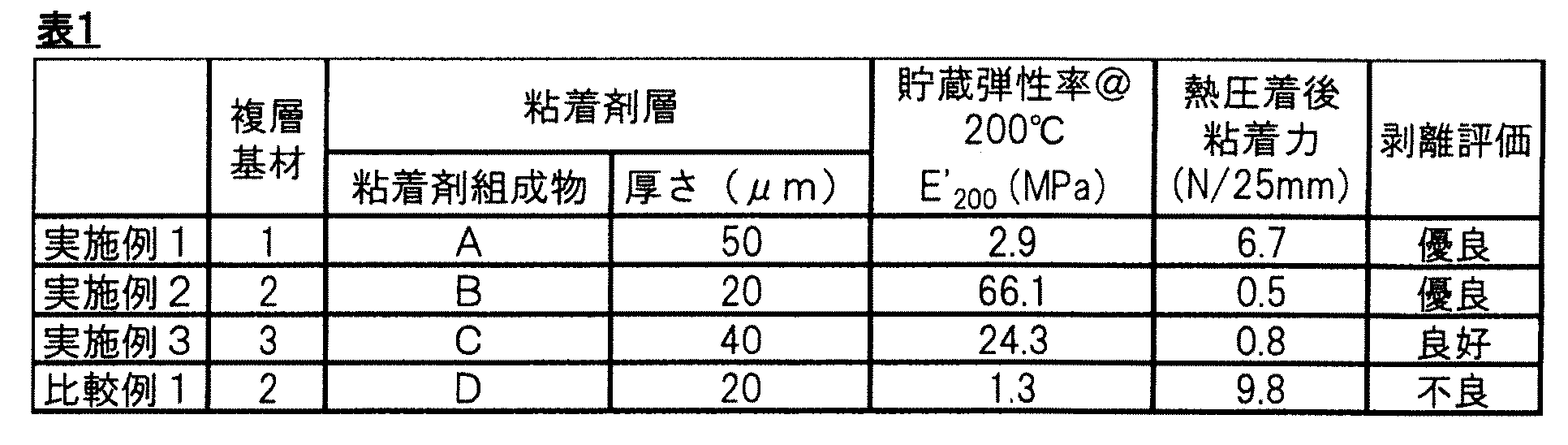
[Comparative Example 1]
A pressure-sensitive adhesive tape was produced in the same manner as in Example 1 except that the multilayer substrate 2 and the pressure-sensitive adhesive composition D were used and the thickness of the pressure-sensitive adhesive layer was 20 μm. The adhesive strength after thermocompression bonding of the obtained adhesive tape was measured, and peeling evaluation was performed.
複層基材2および粘着剤組成物Dを用い、粘着剤層の厚さを20μmとした以外は、実施例1と同様にして、粘着テープを作製した。得られた粘着テープの熱圧着後粘着力を測定し、また剥離評価を行った。
A pressure-sensitive adhesive tape was produced in the same manner as in Example 1 except that the multilayer substrate 2 and the pressure-sensitive adhesive composition D were used and the thickness of the pressure-sensitive adhesive layer was 20 μm. The adhesive strength after thermocompression bonding of the obtained adhesive tape was measured, and peeling evaluation was performed.
以上の結果から、硬化後貯蔵弾性率E’200が1.5MPa以上であれば、剥離用テープの熱圧着を行っても、ヒートシール部におけるチップ転写不良がなく、ピックアップテープまたは接着テープにチップを良好に転写できることが分かる。また、実施例、比較例に詳細に記載した粘着テープの他、各種の粘着テープを用いた試験によりE’200が1.5MPa以上であれば、良好な結果が得られることを確認した。
From the above results, when the post-curing storage elastic modulus E ′ 200 is 1.5 MPa or more, there is no chip transfer failure in the heat seal portion even when the peeling tape is thermocompression bonded, and the chip is placed on the pickup tape or adhesive tape. It can be seen that it can be transferred well. In addition to the adhesive tapes described in detail in Examples and Comparative Examples, it was confirmed by tests using various adhesive tapes that good results were obtained when E ′ 200 was 1.5 MPa or more.
10…粘着テープ(バックグラインドテープ)
11…基材
12…粘着剤層
20…チップ群
21…チップ
30…ピックアップテープ
40…リングフレーム
50…剥離用テープ 10 ... Adhesive tape (Back grind tape)
DESCRIPTION OF SYMBOLS 11 ...Base material 12 ... Adhesive layer 20 ... Chip group 21 ... Chip 30 ... Pickup tape 40 ... Ring frame 50 ... Stripping tape
11…基材
12…粘着剤層
20…チップ群
21…チップ
30…ピックアップテープ
40…リングフレーム
50…剥離用テープ 10 ... Adhesive tape (Back grind tape)
DESCRIPTION OF SYMBOLS 11 ...
Claims (4)
- 基材と、その片面に設けられた粘着剤層とを含む粘着テープであって、
前記粘着剤層が、エネルギー線硬化性粘着剤からなり、
エネルギー線照射して硬化した後の粘着剤の200℃における貯蔵弾性率E’200が1.5MPa以上である粘着テープ。 A pressure-sensitive adhesive tape comprising a base material and a pressure-sensitive adhesive layer provided on one side thereof,
The pressure-sensitive adhesive layer is made of an energy ray-curable pressure-sensitive adhesive,
The adhesive tape whose storage elastic modulus E'200 in 200 degreeC of the adhesive after hardening by energy ray irradiation is 1.5 Mpa or more. - 半導体ウエハ表面に溝が形成された半導体ウエハの表面にバックグラインドテープを貼付して、裏面を研削して、その研削により半導体ウエハを半導体チップに個片化し、その後個片化されたチップ群をピックアップテープまたは接着テープに転写する工程を含む半導体装置の製造方法において、前記バックグラインドテープとして使用される、請求項1に記載の粘着テープ。 A back grind tape is affixed to the surface of the semiconductor wafer having a groove formed on the surface of the semiconductor wafer, the back surface is ground, and the semiconductor wafer is divided into semiconductor chips by the grinding. The pressure-sensitive adhesive tape according to claim 1, wherein the pressure-sensitive adhesive tape is used as the back grind tape in a semiconductor device manufacturing method including a step of transferring to a pickup tape or an adhesive tape.
- 半導体ウエハ表面に溝が形成された半導体ウエハの表面にバックグラインドテープを貼付して、裏面を研削して、その研削により半導体ウエハを半導体チップに個片化し、その後個片化されたチップ群をピックアップテープまたは接着テープに転写する工程を含む半導体装置の製造方法において、前記バックグラインドテープとして請求項1に記載の粘着テープを使用する半導体装置の製造方法。 A back grind tape is affixed to the surface of the semiconductor wafer having a groove formed on the surface of the semiconductor wafer, the back surface is ground, and the semiconductor wafer is divided into semiconductor chips by the grinding. The manufacturing method of the semiconductor device including the process of transferring to a pick-up tape or an adhesive tape, The manufacturing method of the semiconductor device which uses the adhesive tape of Claim 1 as the said back grind tape.
- 請求項1に記載の粘着テープの使用であって、半導体ウエハ表面に溝が形成された半導体ウエハの表面にバックグラインドテープを貼付して、裏面を研削して、その研削により半導体ウエハを半導体チップに個片化し、その後個片化されたチップ群をピックアップテープまたは接着テープに転写する工程を含む半導体装置の製造方法における、前記バックグラインドテープとしての使用。 2. The use of the adhesive tape according to claim 1, wherein a back grind tape is applied to the surface of the semiconductor wafer having a groove formed on the surface of the semiconductor wafer, the back surface is ground, and the semiconductor wafer is then ground by the grinding. Use as the back grind tape in a method of manufacturing a semiconductor device including a step of transferring the chip group into individual pickups and then transferring the divided chips to a pickup tape or an adhesive tape.
Priority Applications (3)
| Application Number | Priority Date | Filing Date | Title |
|---|---|---|---|
| JP2020508292A JP7381447B2 (en) | 2018-03-20 | 2019-03-14 | Adhesive tape and semiconductor device manufacturing method |
| KR1020207026478A KR20200130309A (en) | 2018-03-20 | 2019-03-14 | Adhesive tape and manufacturing method of semiconductor device |
| CN201980020566.1A CN111868193A (en) | 2018-03-20 | 2019-03-14 | Adhesive tape and method for manufacturing semiconductor device |
Applications Claiming Priority (2)
| Application Number | Priority Date | Filing Date | Title |
|---|---|---|---|
| JP2018-053332 | 2018-03-20 | ||
| JP2018053332A JP2018115332A (en) | 2018-03-20 | 2018-03-20 | Pressure-sensitive adhesive tape and production method of semiconductor device |
Publications (1)
| Publication Number | Publication Date |
|---|---|
| WO2019181731A1 true WO2019181731A1 (en) | 2019-09-26 |
Family
ID=62983802
Family Applications (1)
| Application Number | Title | Priority Date | Filing Date |
|---|---|---|---|
| PCT/JP2019/010553 WO2019181731A1 (en) | 2018-03-20 | 2019-03-14 | Adhesive tape, and method for producing semiconductor device |
Country Status (5)
| Country | Link |
|---|---|
| JP (2) | JP2018115332A (en) |
| KR (1) | KR20200130309A (en) |
| CN (1) | CN111868193A (en) |
| TW (1) | TW201942961A (en) |
| WO (1) | WO2019181731A1 (en) |
Cited By (4)
| Publication number | Priority date | Publication date | Assignee | Title |
|---|---|---|---|---|
| CN113410164A (en) * | 2021-06-15 | 2021-09-17 | 西安微电子技术研究所 | Single-chip DAF adhesive tape die bonding method |
| WO2021251420A1 (en) * | 2020-06-10 | 2021-12-16 | 三井化学東セロ株式会社 | Method for producing electronic device |
| WO2021251422A1 (en) * | 2020-06-10 | 2021-12-16 | 三井化学東セロ株式会社 | Method for producing electronic device |
| JP7453831B2 (en) | 2020-03-31 | 2024-03-21 | マクセル株式会社 | Laminated body with self-healing properties, method for manufacturing the same, and method for using the same |
Families Citing this family (1)
| Publication number | Priority date | Publication date | Assignee | Title |
|---|---|---|---|---|
| CN117015843A (en) * | 2021-03-22 | 2023-11-07 | 琳得科株式会社 | Adhesive tape for semiconductor processing and method for manufacturing semiconductor device |
Citations (6)
| Publication number | Priority date | Publication date | Assignee | Title |
|---|---|---|---|---|
| JP2004043762A (en) * | 2001-08-27 | 2004-02-12 | Hitachi Chem Co Ltd | Adhesive sheet, semiconductor device, and production method of the sheet |
| WO2009110426A1 (en) * | 2008-03-03 | 2009-09-11 | リンテック株式会社 | Adhesive sheet |
| JP2011105854A (en) * | 2009-11-18 | 2011-06-02 | Hitachi Maxell Ltd | Self-adhesive tape |
| WO2015156389A1 (en) * | 2014-04-11 | 2015-10-15 | リンテック株式会社 | Base for back grind tapes, and back grind tape |
| JP2016146437A (en) * | 2015-02-09 | 2016-08-12 | 積水化学工業株式会社 | Method for treating wafer |
| WO2017150676A1 (en) * | 2016-03-03 | 2017-09-08 | リンテック株式会社 | Adhesive tape for semiconductor processing and method for producing semiconductor device |
Family Cites Families (9)
| Publication number | Priority date | Publication date | Assignee | Title |
|---|---|---|---|---|
| JP4707805B2 (en) | 2000-08-08 | 2011-06-22 | 三井化学株式会社 | Adhesive film for protecting semiconductor wafer surface and method for protecting semiconductor wafer surface using the same |
| JP4075801B2 (en) * | 2001-08-27 | 2008-04-16 | 日立化成工業株式会社 | Adhesive sheet, semiconductor device and manufacturing method thereof |
| JP2012209385A (en) | 2011-03-29 | 2012-10-25 | Lintec Corp | Pickup tape and method of manufacturing chipped components |
| KR102268694B1 (en) | 2014-01-21 | 2021-06-23 | 린텍 가부시키가이샤 | Adhesive sheet for wafer protection |
| US9905451B2 (en) | 2014-03-03 | 2018-02-27 | Lintec Corporation | Sheet for semiconductor-related-member processing and method of manufacturing chips using the sheet |
| EP3131413A4 (en) | 2014-04-10 | 2017-08-30 | Archer-Daniels-Midland Company | Synthesis of reduced sugar alcohols, furan derivatives |
| JP5823591B1 (en) | 2014-10-01 | 2015-11-25 | 古河電気工業株式会社 | Adhesive tape for protecting semiconductor wafer surface and method for processing semiconductor wafer |
| SG11201804425RA (en) * | 2016-03-03 | 2018-09-27 | Lintec Corp | Adhesive tape for semiconductor processing and method for producing semiconductor device |
| KR102441629B1 (en) * | 2016-10-03 | 2022-09-07 | 린텍 가부시키가이샤 | Adhesive tape for semiconductor processing and manufacturing method of semiconductor device |
-
2018
- 2018-03-20 JP JP2018053332A patent/JP2018115332A/en active Pending
-
2019
- 2019-03-14 CN CN201980020566.1A patent/CN111868193A/en active Pending
- 2019-03-14 KR KR1020207026478A patent/KR20200130309A/en not_active Application Discontinuation
- 2019-03-14 WO PCT/JP2019/010553 patent/WO2019181731A1/en active Application Filing
- 2019-03-14 JP JP2020508292A patent/JP7381447B2/en active Active
- 2019-03-19 TW TW108109275A patent/TW201942961A/en unknown
Patent Citations (6)
| Publication number | Priority date | Publication date | Assignee | Title |
|---|---|---|---|---|
| JP2004043762A (en) * | 2001-08-27 | 2004-02-12 | Hitachi Chem Co Ltd | Adhesive sheet, semiconductor device, and production method of the sheet |
| WO2009110426A1 (en) * | 2008-03-03 | 2009-09-11 | リンテック株式会社 | Adhesive sheet |
| JP2011105854A (en) * | 2009-11-18 | 2011-06-02 | Hitachi Maxell Ltd | Self-adhesive tape |
| WO2015156389A1 (en) * | 2014-04-11 | 2015-10-15 | リンテック株式会社 | Base for back grind tapes, and back grind tape |
| JP2016146437A (en) * | 2015-02-09 | 2016-08-12 | 積水化学工業株式会社 | Method for treating wafer |
| WO2017150676A1 (en) * | 2016-03-03 | 2017-09-08 | リンテック株式会社 | Adhesive tape for semiconductor processing and method for producing semiconductor device |
Cited By (9)
| Publication number | Priority date | Publication date | Assignee | Title |
|---|---|---|---|---|
| JP7453831B2 (en) | 2020-03-31 | 2024-03-21 | マクセル株式会社 | Laminated body with self-healing properties, method for manufacturing the same, and method for using the same |
| WO2021251420A1 (en) * | 2020-06-10 | 2021-12-16 | 三井化学東セロ株式会社 | Method for producing electronic device |
| WO2021251422A1 (en) * | 2020-06-10 | 2021-12-16 | 三井化学東セロ株式会社 | Method for producing electronic device |
| JPWO2021251420A1 (en) * | 2020-06-10 | 2021-12-16 | ||
| JPWO2021251422A1 (en) * | 2020-06-10 | 2021-12-16 | ||
| JP7440632B2 (en) | 2020-06-10 | 2024-02-28 | 三井化学東セロ株式会社 | Electronic device manufacturing method |
| JP7440633B2 (en) | 2020-06-10 | 2024-02-28 | 三井化学東セロ株式会社 | Electronic device manufacturing method |
| CN113410164A (en) * | 2021-06-15 | 2021-09-17 | 西安微电子技术研究所 | Single-chip DAF adhesive tape die bonding method |
| CN113410164B (en) * | 2021-06-15 | 2024-04-09 | 珠海天成先进半导体科技有限公司 | Single-chip DAF adhesive tape crystal bonding method |
Also Published As
| Publication number | Publication date |
|---|---|
| JPWO2019181731A1 (en) | 2021-04-15 |
| KR20200130309A (en) | 2020-11-18 |
| CN111868193A (en) | 2020-10-30 |
| JP2018115332A (en) | 2018-07-26 |
| TW201942961A (en) | 2019-11-01 |
| JP7381447B2 (en) | 2023-11-15 |
Similar Documents
| Publication | Publication Date | Title |
|---|---|---|
| JP7207778B2 (en) | Adhesive tape for semiconductor processing and method for manufacturing semiconductor device | |
| WO2019181731A1 (en) | Adhesive tape, and method for producing semiconductor device | |
| JP7326248B2 (en) | Adhesive tape and method for manufacturing semiconductor device | |
| TW202020096A (en) | Adhesive tape for semiconductor processing and method for producing semiconductor device | |
| TW202016234A (en) | Semiconductor processing adhesive tape and method of manufacturing semiconductor device | |
| JP7381448B2 (en) | Adhesive tape and semiconductor device manufacturing method | |
| JP7326249B2 (en) | Adhesive tape and method for manufacturing semiconductor device | |
| KR102642081B1 (en) | Manufacturing method of adhesive tape and semiconductor device | |
| JP7069116B2 (en) | Base material for back grind tape | |
| JP7339941B2 (en) | Adhesive tape and method for manufacturing semiconductor device | |
| CN117099185A (en) | Adhesive tape for semiconductor processing and method for manufacturing semiconductor device |
Legal Events
| Date | Code | Title | Description |
|---|---|---|---|
| 121 | Ep: the epo has been informed by wipo that ep was designated in this application |
Ref document number: 19772597 Country of ref document: EP Kind code of ref document: A1 |
|
| ENP | Entry into the national phase |
Ref document number: 2020508292 Country of ref document: JP Kind code of ref document: A |
|
| NENP | Non-entry into the national phase |
Ref country code: DE |
|
| 122 | Ep: pct application non-entry in european phase |
Ref document number: 19772597 Country of ref document: EP Kind code of ref document: A1 |