WO2019181707A1 - Glass substrate, liquid crystal antenna and high-frequency device - Google Patents
Glass substrate, liquid crystal antenna and high-frequency device Download PDFInfo
- Publication number
- WO2019181707A1 WO2019181707A1 PCT/JP2019/010424 JP2019010424W WO2019181707A1 WO 2019181707 A1 WO2019181707 A1 WO 2019181707A1 JP 2019010424 W JP2019010424 W JP 2019010424W WO 2019181707 A1 WO2019181707 A1 WO 2019181707A1
- Authority
- WO
- WIPO (PCT)
- Prior art keywords
- glass substrate
- less
- substrate according
- glass
- substrate
- Prior art date
Links
Images

Classifications
-
- C—CHEMISTRY; METALLURGY
- C03—GLASS; MINERAL OR SLAG WOOL
- C03C—CHEMICAL COMPOSITION OF GLASSES, GLAZES OR VITREOUS ENAMELS; SURFACE TREATMENT OF GLASS; SURFACE TREATMENT OF FIBRES OR FILAMENTS MADE FROM GLASS, MINERALS OR SLAGS; JOINING GLASS TO GLASS OR OTHER MATERIALS
- C03C4/00—Compositions for glass with special properties
-
- H—ELECTRICITY
- H01—ELECTRIC ELEMENTS
- H01Q—ANTENNAS, i.e. RADIO AERIALS
- H01Q1/00—Details of, or arrangements associated with, antennas
- H01Q1/36—Structural form of radiating elements, e.g. cone, spiral, umbrella; Particular materials used therewith
- H01Q1/38—Structural form of radiating elements, e.g. cone, spiral, umbrella; Particular materials used therewith formed by a conductive layer on an insulating support
-
- H—ELECTRICITY
- H01—ELECTRIC ELEMENTS
- H01Q—ANTENNAS, i.e. RADIO AERIALS
- H01Q1/00—Details of, or arrangements associated with, antennas
- H01Q1/36—Structural form of radiating elements, e.g. cone, spiral, umbrella; Particular materials used therewith
- H01Q1/364—Structural form of radiating elements, e.g. cone, spiral, umbrella; Particular materials used therewith using a particular conducting material, e.g. superconductor
-
- C—CHEMISTRY; METALLURGY
- C03—GLASS; MINERAL OR SLAG WOOL
- C03C—CHEMICAL COMPOSITION OF GLASSES, GLAZES OR VITREOUS ENAMELS; SURFACE TREATMENT OF GLASS; SURFACE TREATMENT OF FIBRES OR FILAMENTS MADE FROM GLASS, MINERALS OR SLAGS; JOINING GLASS TO GLASS OR OTHER MATERIALS
- C03C19/00—Surface treatment of glass, not in the form of fibres or filaments, by mechanical means
-
- C—CHEMISTRY; METALLURGY
- C03—GLASS; MINERAL OR SLAG WOOL
- C03C—CHEMICAL COMPOSITION OF GLASSES, GLAZES OR VITREOUS ENAMELS; SURFACE TREATMENT OF GLASS; SURFACE TREATMENT OF FIBRES OR FILAMENTS MADE FROM GLASS, MINERALS OR SLAGS; JOINING GLASS TO GLASS OR OTHER MATERIALS
- C03C3/00—Glass compositions
- C03C3/04—Glass compositions containing silica
- C03C3/076—Glass compositions containing silica with 40% to 90% silica, by weight
- C03C3/083—Glass compositions containing silica with 40% to 90% silica, by weight containing aluminium oxide or an iron compound
- C03C3/085—Glass compositions containing silica with 40% to 90% silica, by weight containing aluminium oxide or an iron compound containing an oxide of a divalent metal
- C03C3/087—Glass compositions containing silica with 40% to 90% silica, by weight containing aluminium oxide or an iron compound containing an oxide of a divalent metal containing calcium oxide, e.g. common sheet or container glass
-
- C—CHEMISTRY; METALLURGY
- C03—GLASS; MINERAL OR SLAG WOOL
- C03C—CHEMICAL COMPOSITION OF GLASSES, GLAZES OR VITREOUS ENAMELS; SURFACE TREATMENT OF GLASS; SURFACE TREATMENT OF FIBRES OR FILAMENTS MADE FROM GLASS, MINERALS OR SLAGS; JOINING GLASS TO GLASS OR OTHER MATERIALS
- C03C3/00—Glass compositions
- C03C3/04—Glass compositions containing silica
- C03C3/076—Glass compositions containing silica with 40% to 90% silica, by weight
- C03C3/089—Glass compositions containing silica with 40% to 90% silica, by weight containing boron
- C03C3/091—Glass compositions containing silica with 40% to 90% silica, by weight containing boron containing aluminium
-
- C—CHEMISTRY; METALLURGY
- C03—GLASS; MINERAL OR SLAG WOOL
- C03C—CHEMICAL COMPOSITION OF GLASSES, GLAZES OR VITREOUS ENAMELS; SURFACE TREATMENT OF GLASS; SURFACE TREATMENT OF FIBRES OR FILAMENTS MADE FROM GLASS, MINERALS OR SLAGS; JOINING GLASS TO GLASS OR OTHER MATERIALS
- C03C4/00—Compositions for glass with special properties
- C03C4/0085—Compositions for glass with special properties for UV-transmitting glass
-
- C—CHEMISTRY; METALLURGY
- C03—GLASS; MINERAL OR SLAG WOOL
- C03C—CHEMICAL COMPOSITION OF GLASSES, GLAZES OR VITREOUS ENAMELS; SURFACE TREATMENT OF GLASS; SURFACE TREATMENT OF FIBRES OR FILAMENTS MADE FROM GLASS, MINERALS OR SLAGS; JOINING GLASS TO GLASS OR OTHER MATERIALS
- C03C4/00—Compositions for glass with special properties
- C03C4/16—Compositions for glass with special properties for dielectric glass
-
- H—ELECTRICITY
- H01—ELECTRIC ELEMENTS
- H01P—WAVEGUIDES; RESONATORS, LINES, OR OTHER DEVICES OF THE WAVEGUIDE TYPE
- H01P3/00—Waveguides; Transmission lines of the waveguide type
- H01P3/02—Waveguides; Transmission lines of the waveguide type with two longitudinal conductors
- H01P3/08—Microstrips; Strip lines
-
- H—ELECTRICITY
- H01—ELECTRIC ELEMENTS
- H01Q—ANTENNAS, i.e. RADIO AERIALS
- H01Q1/00—Details of, or arrangements associated with, antennas
- H01Q1/12—Supports; Mounting means
- H01Q1/22—Supports; Mounting means by structural association with other equipment or articles
- H01Q1/2283—Supports; Mounting means by structural association with other equipment or articles mounted in or on the surface of a semiconductor substrate as a chip-type antenna or integrated with other components into an IC package
-
- H—ELECTRICITY
- H01—ELECTRIC ELEMENTS
- H01Q—ANTENNAS, i.e. RADIO AERIALS
- H01Q15/00—Devices for reflection, refraction, diffraction or polarisation of waves radiated from an antenna, e.g. quasi-optical devices
- H01Q15/0006—Devices acting selectively as reflecting surface, as diffracting or as refracting device, e.g. frequency filtering or angular spatial filtering devices
- H01Q15/0013—Devices acting selectively as reflecting surface, as diffracting or as refracting device, e.g. frequency filtering or angular spatial filtering devices said selective devices working as frequency-selective reflecting surfaces, e.g. FSS, dichroic plates, surfaces being partly transmissive and reflective
-
- H—ELECTRICITY
- H01—ELECTRIC ELEMENTS
- H01Q—ANTENNAS, i.e. RADIO AERIALS
- H01Q9/00—Electrically-short antennas having dimensions not more than twice the operating wavelength and consisting of conductive active radiating elements
- H01Q9/04—Resonant antennas
- H01Q9/0407—Substantially flat resonant element parallel to ground plane, e.g. patch antenna
Definitions
- the present invention relates to a glass substrate, and a liquid crystal antenna and a high-frequency device having the glass substrate.
- an insulating substrate such as a resin substrate, a ceramic substrate, or a glass substrate is used as a circuit substrate used in such high-frequency communication equipment and electronic devices. Insulating substrates used for communication equipment and electronic devices for high frequency applications are required to reduce transmission loss based on dielectric loss, conductor loss, etc., in order to ensure characteristics such as quality and strength of high frequency signals. .
- Patent Document 1 discloses that the transmission loss can be maintained at a conventional level and the crosstalk noise can be suppressed by setting the dielectric loss tangent of the insulating substrate and the wiring width and surface roughness of the wiring layer to a specific range.
- Patent Document 2 discloses that an electronic circuit board having a small relative dielectric constant or dielectric loss can be obtained by using lead-free glass having a specific composition.
- resin substrates have low rigidity due to their characteristics. For this reason, the resin substrate is difficult to apply when the semiconductor package product requires rigidity (strength). In addition, it is difficult to increase the surface smoothness of the ceramic substrate, and as a result, the conductor loss due to the conductor formed on the substrate surface tends to increase.
- the glass substrate has high rigidity, it is easy to reduce the size and thickness of the package, has excellent surface smoothness, and is easy to increase in size as the substrate itself. .
- the conventional glass substrate has a large dielectric loss tangent particularly in the GHz band, and it is difficult to maintain characteristics such as quality and strength of the high-frequency signal. Further, when the substrate is used as a perforated substrate in which a hole is formed in the substrate, the glass substrate is likely to be broken by a thermal shock generated due to a temperature difference in the substrate generated during laser processing for drilling.
- an object of the present invention is to provide a glass substrate that can reduce the dielectric loss of a high-frequency signal and is excellent in thermal shock resistance, and a liquid crystal antenna and a high-frequency device using the glass substrate.
- the temperature represented by the product of the Young's modulus and the average thermal expansion coefficient at 50 to 350 ° C. is set to a predetermined value or less, thereby increasing the temperature It was found to be excellent in resistance to thermal shock applied by change. Accordingly, it can be suitably used for a substrate used in an environment with a large temperature change such as a liquid crystal antenna or the like, a substrate for a high frequency circuit that performs drilling with a laser or the like.
- the glass substrate according to the present invention satisfies the relationship of ⁇ Young's modulus (GPa) ⁇ 50 to 350 ° C. average thermal expansion coefficient (ppm / ° C.) ⁇ ⁇ 300 (GPa ⁇ ppm / ° C.), 20 ° C., 35 GHz And the dielectric loss tangent at 20 ° C. and 35 GHz is 0.006 or less.
- the glass substrate is used for a liquid crystal antenna or a high-frequency circuit.
- one mode of the liquid crystal antenna or the high-frequency device according to the present invention includes the glass substrate.
- the dielectric loss of the high frequency signal can be reduced. Furthermore, since it has excellent thermal shock resistance, it is suitable as a substrate used in an environment with a large temperature change, a substrate for drilling with a laser, or the like. Therefore, a high-performance and practical liquid crystal antenna and high-frequency device can be provided.
- FIG. 1 is a cross-sectional view showing an example of the configuration of a high-frequency circuit.
- the content of each component in the glass substrate is a molar percentage display based on oxide. “High frequency” means that the frequency is 10 GHz or more, preferably more than 30 GHz, more preferably 35 GHz or more.
- the glass substrate according to the present invention (hereinafter sometimes simply referred to as “substrate”) has ⁇ Young's modulus (GPa) ⁇ average thermal expansion coefficient (ppm / ° C.) at 50 to 350 ° C. ⁇ ⁇ 300 (GPa ⁇ ppm / ° C. ),
- the relative dielectric constant at 20 ° C. and 35 GHz is 10 or less, and the dielectric loss tangent at 20 ° C. and 35 GHz is 0.006 or less.
- the value represented by the formula ⁇ Young's modulus (GPa) ⁇ average coefficient of thermal expansion (ppm / ° C.) at 50 to 350 ° C. ⁇ (hereinafter sometimes referred to as formula 2) shall be 300 GPa ⁇ ppm / ° C. or less.
- the value represented by Formula 2 is preferably 280 GPa ⁇ ppm / ° C. or less, more preferably 250 GPa ⁇ ppm / ° C. or less, still more preferably 220 GPa ⁇ ppm / ° C. or less, and even more preferably 200 GPa ⁇ ppm / ° C. or less.
- the lower limit is not particularly limited, but is preferably 100 GPa ⁇ ppm / ° C. or more from the viewpoint of securing the rigidity of the substrate and obtaining a substrate that is easy to manufacture.
- the Young's modulus of the glass substrate is preferably 70 GPa or less, more preferably 67 GPa or less, further preferably 64 GPa or less, and further preferably 60 GPa or less.
- the Young's modulus is preferably 40 GPa or more, preferably 50 GPa or more from the viewpoint of suppressing the amount of bending of the substrate during the manufacturing process (wafer process) of the high-frequency device and suppressing the occurrence of manufacturing defects. Is more preferable, and 55 GPa or more is more preferable.
- the Young's modulus can be adjusted by the composition and thermal history of the glass used as the substrate.
- the Young's modulus can be measured by the ultrasonic pulse method according to the method defined in JIS Z 2280 (1993).
- the average coefficient of thermal expansion at 50 to 350 ° C. is preferably smaller, preferably 5 ppm / ° C. or less, more preferably 4 ppm / ° C. or less, further preferably 3.5 ppm / ° C. or less, and more preferably 3.3 ppm / ° C. or less. Further preferred. In addition, by reducing the average thermal expansion coefficient, it is possible to more appropriately adjust the difference in thermal expansion coefficient with other members when manufacturing a device or the like using the substrate.
- the lower limit is not particularly limited, but is preferably 1.0 ppm / ° C. or more, more preferably 2.0 ppm / ° C. or more from the viewpoint of obtaining thermophysical properties suitable for molding.
- the thermal expansion coefficient can be adjusted by the content of the alkali metal oxide or alkaline earth metal oxide or the thermal history, among the glass composition as the substrate.
- the average coefficient of thermal expansion at 50 to 350 ° C. can be measured using a differential thermal dilatometer according to the method specified in JIS R3102 (1995).
- the dielectric loss in the high frequency region can be reduced by reducing the relative dielectric constant and dielectric loss tangent of the glass substrate.
- the relative dielectric constant at 20 ° C. and 35 GHz is 10 or less, and the dielectric loss tangent (tan ⁇ ) is 0.006 or less.
- the relative dielectric constant is preferably 8 or less, more preferably 6 or less, still more preferably 5 or less, and even more preferably 4.5 or less.
- the lower limit of the relative dielectric constant is not particularly limited, but is usually 4.0 or more.
- the dielectric loss tangent is preferably 0.005 or less, more preferably 0.004 or less, further preferably 0.0035 or less, and further preferably 0.003 or less.
- the lower limit of the dielectric loss tangent is not particularly limited, but is usually 0.0005 or more.
- the relative dielectric constant at 20 ° C. and 10 GHz is preferably 10 or less, and the dielectric loss tangent (tan ⁇ ) is preferably 0.006 or less.
- the relative dielectric constant is more preferably 8 or less, further preferably 6 or less, still more preferably 5 or less, and particularly preferably 4.5 or less.
- the lower limit of the relative dielectric constant is not particularly limited, but is usually 4.0 or more.
- the dielectric loss tangent is more preferably 0.005 or less, further preferably 0.004 or less, still more preferably 0.0035 or less, and particularly preferably 0.003 or less.
- the lower limit of the dielectric loss tangent is not particularly limited, but is usually 0.0005 or more.
- the relative dielectric constant and electrostatic tangent value at 20 ° C. and 35 GHz close to the relative dielectric constant and electrostatic tangent value at 20 ° C. and 10 GHz, respectively, by reducing the frequency dependence (dielectric dispersion), This is preferable because the frequency characteristics of the dielectric characteristics are not easily changed, and the design change can be small even when the frequency at the time of use is different.
- the relative dielectric constant and dielectric loss tangent can be adjusted by the composition of the glass serving as the substrate.
- the relative dielectric constant and dielectric loss tangent can be measured using a cavity resonator and a vector network analyzer in accordance with the method defined in JIS R1641 (2007).
- the surface roughness of the end face of the substrate is preferably 1.5 nm or less, more preferably 1.0 nm or less, still more preferably 0.8 nm or less, and even more preferably 0.5 nm or less as the value of arithmetic average roughness Ra. Preferably, 0.3 nm or less is particularly preferable.
- the end surface of the glass substrate is a surface parallel to the thickness direction of the substrate.
- Arithmetic mean roughness Ra means a value obtained in accordance with JIS B0601 (2001).
- a processing method such as polishing treatment or etching using a chemical solution such as hydrofluoric acid can be mentioned.
- an abrasive mainly composed of cerium oxide or colloidal silica and mechanical polishing using an abrasive pad, an abrasive, an abrasive slurry using an acidic or alkaline liquid as a dispersion medium, and an abrasive pad are used.
- the chemical mechanical polishing used, chemical polishing using an acidic solution or an alkaline solution as an etching solution, or the like can be applied.
- These polishing processes are applied according to the surface roughness of the glass plate used as the raw material of the glass substrate. For example, preliminary polishing and finish polishing may be combined and applied.
- the substrate is likely to be cracked, cracked, chipped, etc. starting from the end surface, it is preferable that at least a part of the end surface is chamfered to improve the strength of the substrate, and the chamfered shape of the end surface is obtuse. It is more preferable because the strength can be further improved.
- the chamfering include C chamfering, R chamfering, yarn chamfering, and the like, and chamfering may be performed with a complicated shape combining these. Among them, C chamfering and R chamfering are preferable.
- C chamfering is a chamfering method in which the corner portion formed by the main surface and the end surface is obliquely dropped, and the angle formed by the surface perpendicular to the main surface of the substrate and the surface after the corner portion is dropped is 120 ° or more. Is more preferable, 135 ° or more is more preferable, and 175 ° or more is more preferable.
- the R chamfering is a chamfering method in which the shape after chamfering is rounded with respect to the C chamfering.
- the arithmetic average roughness Ra of the chamfered surface is preferably 0.2 ⁇ m or less.
- the main surface of the glass substrate is a surface on which a wiring layer is formed when the substrate is used for, for example, a high-frequency circuit, and the surface roughness of the main surface is 1.5 nm or less as the value of the arithmetic average roughness Ra. Even in a high frequency region exceeding 30 GHz, the skin resistance can be reduced with respect to the wiring layer in which the skin effect has occurred, and this is preferable because the conductor loss is reduced.
- the arithmetic average roughness Ra of the main surface of the substrate is more preferably 1.0 nm or less, and further preferably 0.5 nm or less.
- the surface roughness of the main surface can be realized by subjecting the surface of the main surface to a polishing treatment as necessary.
- a polishing treatment a method similar to the polishing treatment on the end face can be employed.
- the shape of the substrate is not particularly limited, but the area of one main surface is 100 cm 2 or more is preferred from the viewpoint of transmission and reception efficiency of the antenna, etc., 225 cm 2 or more is more preferable. Further, preferably from the viewpoint of ease of handling of the substrate is at 100000 2 or less, more preferably 10000 cm 2 or less, more preferably 3600 cm 2 or less.
- the thickness of the substrate is preferably 0.01 mm or more from the viewpoint of maintaining the strength of the substrate, and more preferably 0.05 mm or more. Furthermore, it is more preferably 0.1 mm or more, and more preferably more than 0.2 mm, from the viewpoint that the ultraviolet shielding ability can be increased and a resin deteriorated by ultraviolet rays can be protected.
- it is preferably 2 mm or less, more preferably 1 mm or less from the viewpoints of thinning and miniaturization of a high-frequency device and a liquid crystal antenna using a high-frequency circuit, and improvement of production efficiency. Furthermore, 0.7 mm or less is more preferable, and 0.5 mm or less is more preferable from the point which can raise ultraviolet transmittance and can improve manufacturability using an ultraviolet curable material in manufacturing processes, such as a device and an antenna.
- the substrate has a Vickers hardness of 400 or more because it is difficult to break against mechanical impact, more preferably 450 or more, and even more preferably 500 or more. Moreover, 550 or less is preferable.
- the Vickers hardness can be adjusted by the glass composition in the substrate.
- the Vickers hardness can be measured by a method based on JIS R1310 (2003).
- the crack generation load of the substrate is preferably more than 1.96 N because it is difficult to crack against mechanical impact, more preferably 4.9 N or more, further preferably 9.8 N or more, particularly more than 19.6 N. preferable.
- the crack generation load can be adjusted by the glass composition, thermal history and surface processing on the substrate.
- the crack generation load can be determined by measuring a load with a crack generation rate exceeding 50% using a Vickers hardness tester.
- the density of the substrate is preferably 2.5 g / cm 3 or less from the viewpoint of reducing the weight of a device or antenna having the substrate and reducing the brittleness of the glass and making it difficult to break against thermal shock and mechanical shock.
- 2.4 g / cm 3 or less is more preferable, 2.35 g / cm 3 or less is more preferable, and 2.3 g / cm 3 or less is even more preferable.
- a minimum in particular is not restrict
- the density can be measured by the Archimedes method.
- At least one main surface of the substrate has a compressive stress layer on at least a part of the surface from the viewpoint of being hard to break against thermal shock and mechanical shock.
- the compressive stress layer can be formed by, for example, strengthening treatment, and both physical strengthening treatment and chemical strengthening treatment can be employed. Conventionally known methods can be used for both the physical strengthening treatment and the chemical strengthening treatment.
- the porosity of the substrate is preferably 0.1% or less, more preferably 0.01% or less, and still more preferably 0.001% or less, from the viewpoint of suppressing the generation of noise when a high-frequency device is produced. Further, from the viewpoint of the liquid crystal antenna, 0.0001% or less is preferable in order to suppress the occurrence of defective wiring due to the exposure of open pores on the surface.
- the porosity can be obtained by observing bubbles contained in the glass substrate with an optical microscope, obtaining the number and diameter of the bubbles, and calculating the volume of the bubbles contained per unit volume.
- the transmittance of light with a wavelength of 350 nm of the substrate is preferably 50% or more because an ultraviolet curable material can be used in a lamination process or the like in a manufacturing process of a high-frequency device, an antenna, or the like, and productivity can be improved. Furthermore, 70% or more is more preferable in order to shorten the irradiation time of the ultraviolet ray to the ultraviolet curable material in the manufacturing process of the device, the antenna and the like and reduce the unevenness of the ultraviolet curable material in the thickness direction.
- the transmittance of light having a wavelength of 300 nm of the substrate is preferably 50% or more, more preferably 60% or more, and even more preferably 70% or more. Further, the transmittance of light having a wavelength of 250 nm is preferably 5% or more, more preferably 10% or more, and further preferably 20% or more.
- the transmittance of light having a wavelength of 350 nm is 80% from the viewpoint of providing a function as a protective material by providing the substrate with an ultraviolet shielding ability. Or less, more preferably 60% or less, even more preferably 30% or less, and most preferably 10% or less.
- the transmittance of light having a wavelength of 300 nm of the substrate is preferably 80% or less, more preferably 60% or less, still more preferably 30% or less, and still more preferably 10% or less.
- the transmittance of light having a wavelength of 250 m is preferably 60% or less, more preferably 30% or less, further preferably 10% or less, and still more preferably 5% or less.
- the transmittance of light of each wavelength of the substrate can be measured using a visible ultraviolet spectrophotometer, and an external transmittance including loss due to reflection is used.
- the ⁇ -OH value of the substrate is a value used as an index of the water content of the glass.
- the absorbance of the glass substrate with respect to light having a wavelength of 2.75 to 2.95 ⁇ m is measured, and the maximum value ⁇ max is determined as the value of the substrate. It is a value obtained by dividing by the thickness (mm).
- the ⁇ -OH value is preferably 0.8 mm ⁇ 1 or less because the low dielectric loss property of the substrate can be further improved, preferably 0.6 mm ⁇ 1 or less, more preferably 0.5 mm ⁇ 1 or less. Preferably, 0.4 mm ⁇ 1 or less is even more preferable.
- beta-OH value is more preferably equal to or greater than 0.1 mm -1, further preferably 0.2 mm -1 or higher.
- the ⁇ -OH value can be adjusted by the glass composition in the substrate, the heat source at the time of melting, the melting time, and the raw material.
- the devitrification temperature of the substrate is preferably 1400 ° C. or lower.
- the member temperature of the forming equipment can be lowered when the glass is formed, and the member life can be extended.
- the devitrification temperature is more preferably 1350 ° C. or less, further preferably 1330 ° C. or less, and particularly preferably 1300 ° C. or less.
- Glass devitrification temperature refers to the glass surface obtained by putting crushed glass particles in a platinum dish, heat-treating in an electric furnace controlled at a constant temperature for 17 hours, and observing the sample after the heat treatment with an optical microscope. And the average value of the maximum temperature at which crystals precipitate and the minimum temperature at which crystals do not precipitate.
- the glass on the substrate is amorphous and indicates a solid exhibiting a glass transition. It does not include crystallized glass, which is a mixture of glass and crystal, or a glass sintered body containing a crystalline filler. In addition, about the crystallinity of glass, it can confirm that it is amorphous by, for example, performing an X-ray-diffraction measurement and not having a clear diffraction peak.
- the glass substrate is formed by melting and curing a glass raw material.
- the method for producing the substrate is not particularly limited. For example, a method of forming a general molten glass into a predetermined plate thickness by a float process, cutting it into a desired shape after slow cooling, and the like are applied. be able to.
- substantially does not contain means that it is not contained other than inevitable impurities mixed from raw materials, that is, it is not intentionally contained, and is generally 0.1 mol% or less.
- the present invention is not limited to this.
- Glass is preferably composed mainly of SiO 2.
- “main component” means that the content of SiO 2 is maximum in the proportion of the component in mol% based on the oxide.
- SiO 2 is a network-forming substance, and the content thereof is preferably 40% or more, more preferably 45% or more because glass forming ability and weather resistance can be improved and devitrification can be suppressed.
- 50% or more is even more preferable, and 55% or more is particularly preferable.
- it is preferably 75% or less, more preferably 74% or less, still more preferably 73% or less, and even more preferably 72% or less from the viewpoint of improving the solubility of the glass.
- the total content of Al 2 O 3 and B 2 O 3 (including the case where the content of Al 2 O 3 is 0) is preferably 1% or more because it can enhance the solubility of the glass and the like, and preferably 3% The above is more preferable, 5% or more is further preferable, and 7% or more is more preferable. Further, while maintaining the solubility of glass or the like, since it is possible to increase the low dielectric loss of the substrate, the total content of Al 2 O 3 and B 2 O 3 is preferably 40% or less, more 37% or less Preferably, 35% or less is more preferable, and 33% or less is even more preferable.
- the molar ratio of the content represented by ⁇ Al 2 O 3 / (Al 2 O 3 + B 2 O 3 ) ⁇ is preferably 0.45 or less because the low dielectric loss property of the glass substrate can be improved. 0.4 or less is more preferable, and 0.3 or less is more preferable. Further, the molar ratio of the content represented by ⁇ Al 2 O 3 / (Al 2 O 3 + B 2 O 3 ) ⁇ is preferably 0 or more (including 0), more preferably 0.01 or more, and 0.05 The above is more preferable.
- the content of Al 2 O 3 is preferably 15% or less, more preferably 14% or less, and even more preferably 10% or less because glass solubility and the like can be improved. Moreover, since it is a component which exhibits an effect in improving weather resistance, suppressing phase separation of the glass, lowering the thermal expansion coefficient, etc., Al 2 O 3 may not be contained, but the content in the case of inclusion is 0. More preferably 5% or more.
- the content of B 2 O 3 is preferably 30% or less, more preferably 28% or less, further preferably 26% or less, and still more preferably 24% or less, because acid resistance and strain point can be improved. 23% or less is particularly preferable. Moreover, since it is a component which exhibits an effect for improving the solubility reactivity and lowering the devitrification temperature, the content of B 2 O 3 is preferably 9% or more, more preferably 13% or more, and 16% or more. Further preferred.
- alkaline earth metal oxides include MgO, CaO, SrO, and BaO, all of which function as components that increase the dissolution reactivity of glass.
- the total content of such alkaline earth metal oxides is preferably 13% or less, more preferably 11% or less, further preferably 10% or less, and more preferably 8% or less because the low dielectric loss property of the glass substrate can be enhanced. Is more preferable, and 6% or less is particularly preferable.
- the total content of the alkaline earth metal oxide is preferably 0.1% or more, more preferably 3% or more, and further preferably 5% or more, from the viewpoint that the solubility of the glass can be kept good.
- MgO is not an essential component, but is a component that can increase the Young's modulus without increasing the specific gravity. That is, MgO is a component that can increase the specific elastic modulus, and by containing MgO, the problem of deflection can be reduced, and the fracture toughness value can be improved to increase the glass strength. MgO is a component that improves solubility. Although MgO is not an essential component, the effect of containing MgO can be sufficiently obtained, and since the thermal expansion coefficient can be suppressed from becoming too low, the content is preferably 0.1% or more, and 1% The above is more preferable, and 3% or more is more preferable. On the other hand, from the viewpoint of suppressing an increase in the devitrification temperature, the content of MgO is preferably 13% or less, more preferably 11% or less, and further preferably 9% or less.
- CaO is a component that increases the specific elastic modulus next to MgO in alkaline earth metals and does not excessively lower the strain point, and is a component that improves solubility as well as MgO. Furthermore, it is a component having a feature that it is difficult to increase the devitrification temperature as compared with MgO.
- the content is preferably 0.1% or more, more preferably 1% or more, and even more preferably 3% or more because an effect of containing CaO can be sufficiently obtained. Further, the CaO content is preferably 13% or less, preferably 10% or less from the viewpoint that the average coefficient of thermal expansion does not become too high and the devitrification temperature can be suppressed to prevent devitrification during the production of glass. Is more preferable, and 8% or less is more preferable.
- SrO is a component that improves the solubility without increasing the devitrification temperature of the glass.
- SrO is not an essential component, but since the effect of containing SrO can be sufficiently obtained, the content is preferably 0.1% or more, more preferably 0.5% or more, and further preferably 1% or more, 1.5% or more is still more preferable, and 2% or more is particularly preferable.
- the SrO content is preferably 13% or less, more preferably 10% or less, and even more preferably 7% or less, from the viewpoint of suppressing the average thermal expansion coefficient from becoming too high without increasing the specific gravity. 5% or less is particularly preferable.
- BaO is not an essential component, but is a component that improves the solubility without increasing the devitrification temperature of the glass.
- the content of BaO is preferably 10% or less, more preferably 8% or less, still more preferably 5% or less, still more preferably 3% or less, and particularly preferably substantially not contained.
- the stress applied to the substrate is reduced even when distortion occurs due to the difference in thermal expansion. From the viewpoint of improving impact properties, 280 or less is more preferred, 250 or less is more preferred, 220 or less is more preferred, and 200 or less is particularly preferred. Moreover, although a minimum is not specifically limited, 100 or more are preferable from a viewpoint of obtaining the thermophysical property suitable for shaping
- alkali metal oxides Li 2 O, Na 2 O , K 2 O, Rb 2 O, Cs 2 O and the like.
- the total content of such alkali metal oxides is preferably 5% or less, more preferably 3% or less, further preferably 1% or less, and more preferably 0.2% or less from the viewpoint of enhancing the low dielectric loss of the glass substrate. Even more preferred is 0.1% or less, and most preferred is 0.05% or less.
- Na 2 O and K 2 O are particularly important, and the total content of Na 2 O and K 2 O is preferably in the range of 0.001 to 5%.
- the coexistence of Na 2 O and K 2 O is preferable because the movement of the alkali component can be suppressed, so that the low dielectric loss property of the glass substrate can be improved. That is, the molar ratio of the content represented by ⁇ Na 2 O / (Na 2 O + K 2 O) ⁇ is preferably 0.01 to 0.99, more preferably 0.98 or less, and even more preferably 0.95 or less. 0.9 or less is even more preferable. On the other hand, the molar ratio of the content represented by ⁇ Na 2 O / (Na 2 O + K 2 O) ⁇ is more preferably 0.02 or more, further preferably 0.05 or more, and further preferably 0.1 or more. .
- Fe 2 O 3 is a component that controls the light absorption performance of the glass substrate, such as infrared absorption performance and ultraviolet absorption performance, and 0.012% or less as the Fe content in terms of Fe 2 O 3 as necessary. Can be contained. When the Fe content is 0.012% or less, the low dielectric loss property and ultraviolet transmittance of the glass substrate can be maintained.
- the content is more preferably 0.01% or less, and further preferably 0.005% or less, in order to improve the ultraviolet transmittance.
- the glass substrate is preferably contained in an amount of 0.05% or more as the Fe content in terms of Fe 2 O 3 as necessary from the viewpoint of improving the ultraviolet shielding ability.
- the Fe content is more preferably 0.07% or more, and further preferably 0.1% or more.
- the glass substrate manufacturing method includes a melting step of heating a glass raw material to obtain molten glass, a clarification step of removing bubbles from the molten glass, a molding step of obtaining a glass ribbon by forming the molten glass into a plate shape, and bringing the glass ribbon to room temperature.
- a slow cooling step of slow cooling is included.
- the molten glass may be formed into a block shape, slowly cooled, and then cut and polished to produce a glass substrate.
- raw materials are prepared so as to have a target glass substrate composition, and the raw materials are continuously charged into a melting furnace, preferably heated to about 1450 ° C. to 1750 ° C. to obtain molten glass.
- halides such as oxides, carbonates, nitrates, hydroxides and chlorides can be used.
- strontium nitrate As the nitrate, strontium nitrate, barium nitrate, magnesium nitrate, calcium nitrate and the like can be used. More preferably, strontium nitrate is used.
- the raw material particle size is appropriately selected from a raw material having a large particle size of several hundreds ⁇ m that does not cause undissolved residue to a raw material having a small particle size of about several ⁇ m that does not agglomerate as secondary particles without scattering during conveyance of the material. Can be used. It is also possible to use a granulated body.
- the water content of the raw material can be appropriately adjusted.
- the dissolution conditions such as the ⁇ -OH value and the oxidation-reduction degree of Fe (redox [Fe 2+ / (Fe 2+ + Fe 3+ )]) can be appropriately adjusted and used.
- the clarification step is a step of removing bubbles from the molten glass obtained in the melting step.
- a defoaming method using reduced pressure may be applied, or defoaming may be performed by setting the temperature higher than the melting temperature of the raw material.
- SO 3 and SnO 2 as a fining agent.
- the SO 3 source is preferably a sulfate of at least one element selected from the group consisting of Al, Na, K, Mg, Ca, Sr, and Ba, more preferably an alkaline earth metal sulfate. 4 ⁇ 2H 2 O, SrSO 4 and BaSO 4 is significantly acts to increase the foam, particularly preferred.
- halogen such as Cl or F as a clarifier in the defoaming method using reduced pressure.
- the Cl source is preferably a chloride of at least one element selected from the group consisting of Al, Mg, Ca, Sr and Ba, more preferably a chloride of an alkaline earth metal, and especially, SrCl 2 ⁇ 6H 2. O and BaCl 2 ⁇ 2H 2 O are particularly preferable because they have a remarkable effect of enlarging bubbles and have low deliquescence.
- CaF 2 is The effect of increasing the solubility of the glass raw material is remarkable and more preferable.
- Tin compounds typified by SnO 2 generate O 2 gas in the glass melt.
- SnO 2 is reduced from SnO 2 to SnO at a temperature of 1450 ° C. or more, and O 2 gas is generated and has a function of greatly growing bubbles.
- the glass raw material is heated to about 1450 to 1750 ° C. and melted, so that bubbles in the glass melt are more effectively increased.
- the tin compound in the raw material is prepared so as to be contained at 0.01% or more in terms of SnO 2 with respect to 100% of the total amount of the mother composition.
- the SnO 2 content of 0.01% or more is preferable because a clarification action during melting of the glass raw material can be obtained, more preferably 0.05% or more, and still more preferably 0.10% or more.
- it is preferable that the SnO 2 content is 0.3% or less because the occurrence of coloring and devitrification of the glass is suppressed.
- the content of the tin compound in the alkali-free glass is more preferably 0.25% or less, more preferably 0.2% or less, and more preferably 0.15% or less in terms of SnO 2 with respect to 100% of the total amount of the mother composition. Particularly preferred.
- the forming step is a step of obtaining a glass ribbon by forming the molten glass from which bubbles have been removed in the clarification step into a plate shape.
- the forming process includes a float method in which molten glass is poured onto a molten metal such as tin to obtain a glass ribbon, an overflow down draw method (fusion method) in which the molten glass flows downward from a bowl-shaped member, and a slit.
- fusion method overflow down draw method
- the slow cooling step is a step of cooling the glass ribbon obtained in the molding step under cooling conditions controlled to a room temperature state.
- the glass ribbon is cooled so that the temperature range between the slow cooling point and the strain point of the formed glass is a predetermined average cooling rate, R (° C./min), and further the room temperature state Slowly cool under predetermined conditions.
- R ° C./min
- the predetermined average cooling rate R [cooling rate (R)] will be described below.
- the equivalent cooling rate (R) in the slow cooling process is too large, the glass after cooling tends to remain distorted.
- the equivalent cooling rate which is a parameter reflecting the fictive temperature, becomes too high, and as a result, low dielectric loss characteristics cannot be obtained. Therefore, it is preferable to set R so that the equivalent cooling rate is 800 ° C./min or less.
- the equivalent cooling rate is more preferably 400 ° C./min or less, further preferably 100 ° C./min or less, and particularly preferably 50 ° C./min or less.
- the cooling rate is too low, the time required for the process becomes too long and the productivity is lowered. Therefore, it is preferably set to be 0.1 ° C./min, more preferably 0.5 ° C./min or more, and further preferably 1 ° C./min or more.
- a glass having a target composition to be processed into a cuboid of 10 mm ⁇ 10 mm ⁇ 0.3 to 2.0 mm is held at a strain point of + 170 ° C. for 5 minutes using an infrared heating electric furnace. 25 ° C). At this time, a plurality of glass samples with a cooling rate of 1 ° C./min to 1000 ° C./min are produced.
- n d the refractive index of the plurality of glass samples of the d-line (wavelength 587.6 nm).
- a V block method or a minimum deflection angle method may be used for the measurement.
- the resulting n d by plotting the logarithm of the cooling speed to obtain a calibration curve of the n d with respect to the cooling rate.
- a corresponding cooling rate (referred to as an equivalent cooling rate in the present embodiment) corresponding to the obtained nd is obtained from the calibration curve.
- the manufacturing method of the glass substrate was described, a manufacturing method is not limited to the said embodiment, The deformation
- the crucible made from platinum or the alloy which has platinum as a main component is a melting tank. Or you may use for a clarification tank.
- the raw material is prepared so as to have the composition of the obtained glass substrate, and the platinum crucible containing the raw material is heated in an electric furnace, preferably heated to about 1450 ° C. to 1700 ° C. To do. A platinum stirrer is inserted and stirred for 1 to 3 hours to obtain molten glass.
- the molten glass is poured out onto a carbon plate or a mold, for example, to form a plate or block.
- the glass transition point Tg is maintained at a temperature of about Tg + 50 ° C., and then cooled to about 1 to 10 ° C./min to the vicinity of the strain point. Cool at a cooling rate that does not remain.
- a glass substrate is obtained. Further, the glass substrate obtained by cutting may be gradually cooled to a room temperature state at a predetermined cooling rate after being heated to, for example, about Tg + 50 ° C. By doing in this way, the equivalent cooling temperature of glass can be adjusted.
- the glass substrate of the present invention is a high-frequency device (electronic device) such as a semiconductor device used in a communication device such as a mobile phone, a smartphone, a portable information terminal, or a Wi-Fi device, a surface acoustic wave (SAW) device, a radar.
- a high-frequency device electronic device
- a communication device such as a mobile phone, a smartphone, a portable information terminal, or a Wi-Fi device
- SAW surface acoustic wave
- Suitable for circuit boards such as radar parts such as transceivers and boards such as antenna parts such as liquid crystal antennas, especially because it can reduce dielectric loss of high-frequency signals and has excellent thermal shock resistance. It is more suitable for a high-frequency circuit used for a high-frequency device or a substrate for a liquid crystal antenna.
- the high-frequency circuit board is suitable for high-frequency devices that handle high-frequency signals, particularly high-frequency signals exceeding 30 GHz, and further high-frequency signals exceeding 35 GHz, and reducing the transmission loss of such high-frequency signals. Properties such as quality and strength can be improved.
- FIG. 1 shows an example (cross-sectional view) of the configuration of a high-frequency circuit used in a high-frequency device.
- the circuit substrate 1 is formed on an insulating glass substrate 2 and a first main surface 2a of the glass substrate 2.
- a first wiring layer 3 and a second wiring layer 4 formed on the second main surface 2b of the glass substrate 2 are provided.
- the first and second wiring layers 3 and 4 form a microstrip line as an example of a transmission line.
- the first wiring layer 3 constitutes a signal wiring
- the second wiring layer 4 constitutes a ground line.
- the structure of the first and second wiring layers 3 and 4 is not limited to this, and the wiring layer may be formed only on one main surface of the glass substrate 2.
- the first and second wiring layers 3 and 4 are layers formed of a conductor, and the thickness thereof is usually about 0.1 to 50 ⁇ m.
- the conductors forming the first and second wiring layers 3 and 4 are not particularly limited.
- metals such as copper, gold, silver, aluminum, titanium, chromium, molybdenum, tungsten, platinum, nickel, and the like
- An alloy or a metal compound containing at least one of these metals is used.
- the structure of the first and second wiring layers 3 and 4 is not limited to a single layer structure, and may have a multilayer structure such as a laminated structure of a titanium layer and a copper layer.
- the formation method of the 1st and 2nd wiring layers 3 and 4 is not specifically limited, For example, various well-known formation methods, such as the printing method which used the conductor paste, the dipping method, the plating method, the vapor deposition method, sputtering, etc. Can be applied.
- the glass substrate of the present invention for a high frequency circuit, transmission loss at a high frequency of the circuit substrate can be reduced.
- the transmission loss at a frequency of 35 GHz can be reduced to preferably 1 dB / cm or less, and more preferably to 0.5 dB / cm or less. Therefore, since the characteristics such as the quality and strength of the high-frequency signal, particularly the high-frequency signal exceeding 30 GHz, and further the high-frequency signal exceeding 35 GHz are maintained, a glass substrate and a circuit board suitable for a high-frequency device handling such a high-frequency signal are provided. Can be provided. Thereby, the characteristic and quality of the high frequency device which handles a high frequency signal can be improved.
- the high-frequency circuit board includes a board called a universal board or a perforated board.
- a regular pattern such as a lattice
- copper foil lands are formed on a base insulating board, Copper foil wiring connecting several lands is formed by etching.
- a laser or the like is used for forming or etching the through hole. Examples of the laser include an excimer laser, an infrared laser, a CO 2 laser, and a UV laser.
- the glass substrate of the present invention When forming or etching through-holes, a temperature difference occurs in the glass substrate and a thermal shock is applied, but the glass substrate of the present invention has a high thermal shock resistance, and therefore it is also cracked against the thermal shock. Through holes and etching can be formed.
- a liquid crystal antenna is a satellite communication antenna that uses liquid crystal technology and can control the direction of radio waves to be transmitted and received, and is mainly suitable for vehicles such as ships, airplanes, and automobiles. Since liquid crystal antennas are mainly expected to be used outdoors, stable characteristics in a wide temperature range are required, and heat applied by sudden temperature changes such as ground and sky, squall in a scorching desert, etc. Resistance to impact is also required.
- the use of the glass substrate of the present invention for a liquid crystal antenna is preferable because it can supply stable characteristics even in a wide temperature range, and further has resistance to rapid temperature changes, so that it can be used without cracking.
- Examples 1 to 26 A glass substrate having a composition shown in Tables 1 to 4, a thickness of 0.5 to 10 mm, and a shape of 50 ⁇ 50 mm was prepared.
- the glass substrate was produced by a melting method using a platinum crucible.
- Raw materials such as silica sand were mixed so as to be 1 kg as glass, and a batch was prepared.
- To 100% raw material of the target composition in mass percentage based on oxides, from 0.1% to 1% sulfate converted to SO 3, 0.16% of F, was added Cl 1%.
- the raw material was put in a platinum crucible and melted by heating at a temperature of 1650 ° C. for 3 hours in an electric furnace to obtain molten glass.
- a platinum stirrer was inserted into a platinum crucible and stirred for 1 hour to homogenize the glass.
- the plate glass is placed in an electric furnace having a temperature of about Tg + 50 ° C., held for 1 hour, and then Tg-100 ° C. at a cooling rate of 1 ° C./min. The electric furnace was cooled down to room temperature and then allowed to cool until the glass reached room temperature.
- the glass was formed into a plate shape by cutting and polishing. Further, the end face was chamfered (C / R) with a chamfering device.
- a glass plate chamfering apparatus an apparatus described in Japanese Patent Application Laid-Open No. 2008-49449 is exemplified, which is an apparatus for chamfering an end portion of a glass plate using a rotating grindstone.
- the rotating grindstone may be either a resin bond or a metal bond.
- the abrasive grains used in grinding stone, diamond, cubic boron nitride (CBN), alumina (Al 2 O 3), silicon carbide (SiC), pumice, or any kind of garnet and the like, or a combination thereof are exemplified.
- RO total amount * 1 represents the total content of alkaline earth metal oxides (MgO + CaO + SrO + BaO)
- R 2 O total amount * 2 represents the total amount of alkali metal oxides ( It represents the content of Na 2 O + K 2 O).
- Equation 1 ⁇ 1.02 ⁇ SiO 2 + 3.42 ⁇ Al 2 O using the content in mole percentage based on oxides 3 + 0.74 ⁇ B 2 O 3 + 9.17 ⁇ MgO + 12.55 ⁇ CaO + 13.85 ⁇ SrO + 14.44 ⁇ BaO + 31.61 ⁇ Na 2 O + 20.35 ⁇ K 2 O ⁇ .
- Formula 2 is a value represented by ⁇ Young's modulus (GPa) ⁇ average thermal expansion coefficient (ppm / ° C.) at 50 to 350 ° C. ⁇ .
- Equation 1 The values of Equation 1 are shown in Tables 1 to 4, and the other results are shown in Tables 5 to 8, respectively.
- the values in parentheses in the table are those obtained by calculation, and blank or-means unmeasured.
- the crack generation load When a regular square pyramid-shaped Vickers indenter (diamond indenter) is pushed into the glass surface for 30 seconds in an atmosphere with a relative humidity of about 40%, the ratio of cracks forming outward from all four corners of the indentation is 50%. This is the indentation load.
- the crack generation load can be measured by a commercially available Vickers hardness tester.
- the crack generation load is an average value for 10 or more indentations.
- Transmittance Using a visible ultraviolet spectrophotometer, the transmittance of mirror-polished glass having a predetermined thickness was measured. The transmittance was expressed as an external transmittance including a loss due to reflection, and a value obtained by converting the glass thickness into 0.3 to 0.4 mm.
- the specific modulus was obtained by calculation using the measurement of density and Young's modulus, and the unit was expressed as GPa ⁇ cm 3 / g.
- the glass substrate of the present invention has a small product of the coefficient of thermal expansion and Young's modulus (value expressed by Equation 2) as small as 300 or less.
- Young's modulus value expressed by Equation 2
- tensile stress is unlikely to occur.
- use in an environment in which a rapid temperature change occurs can suppress breakage in a machining process in which a temperature difference is likely to occur.
- the glass substrate of the present invention has a relative dielectric constant of 10 or less at 20 ° C. and 35 GHz, and a dielectric loss tangent at 20 ° C. and 35 GHz of 0.006 or less. Can be reduced.
- the glass substrate of the present invention since the Vickers hardness is small, it can be processed with a light load, and since the crack generation load is large, defects such as microcracks are unlikely to occur, so that a high strength substrate can be obtained.
- the glass substrate of the present invention is excellent in high-frequency signal dielectric loss and exhibits high thermal shock resistance. Therefore, a circuit board using the glass substrate is excellent in high-frequency signal transmission loss and excellent in workability using heat such as laser.
- Such glass substrates and circuit boards are generally used for high-frequency electronic devices that handle high-frequency signals exceeding 10 GHz, particularly high-frequency signals exceeding 30 GHz, and further high-frequency signals of 35 GHz or higher, and liquid crystal used in environments with large temperature changes. It is very useful as a member for devices such as antennas, lasers, and the like that involve drilling.
Abstract
Provided is a glass substrate with which it is possible to reduce dielectric loss in high-frequency signals, and which also has excellent thermal shock resistance. This invention satisfies the relation {Young's modulus (GPa) × average thermal expansion coefficient (ppm/°C) at 50-350°C}≤300 (GPa·ppm/°C), wherein the relative dielectric constant at 20°C and 35 GHz does not exceed 10, and the dielectric dissipation factor at 20°C and 35 GHz does not exceed 0.006.
Description
本発明はガラス基板、並びに、該ガラス基板を有する液晶アンテナ及び高周波デバイスに関する。
The present invention relates to a glass substrate, and a liquid crystal antenna and a high-frequency device having the glass substrate.
携帯電話機、スマートフォン、携帯情報端末、Wi-Fi機器のような通信機器、弾性表面波(SAW)デバイス、レーダ部品、アンテナ部品等の電子デバイスにおいては、通信容量の大容量化や通信速度の高速化等を図るために、信号周波数の高周波化が進められている。このような高周波用途の通信機器及び電子デバイスに用いられる回路基板には、一般的に樹脂基板、セラミックス基板、ガラス基板等の絶縁基板が使用されている。高周波用途の通信機器及び電子デバイスに用いられる絶縁基板には、高周波信号の質や強度等の特性を確保するために、誘電損失や導体損失等に基づく伝送損失を低減することが求められている。
In electronic devices such as mobile phones, smartphones, personal digital assistants, Wi-Fi devices, surface acoustic wave (SAW) devices, radar components, antenna components, etc., the communication capacity is increased and the communication speed is increased. In order to reduce the frequency, signal frequency has been increased. In general, an insulating substrate such as a resin substrate, a ceramic substrate, or a glass substrate is used as a circuit substrate used in such high-frequency communication equipment and electronic devices. Insulating substrates used for communication equipment and electronic devices for high frequency applications are required to reduce transmission loss based on dielectric loss, conductor loss, etc., in order to ensure characteristics such as quality and strength of high frequency signals. .
例えば特許文献1では、絶縁基板の誘電正接並びに配線層の配線幅及び表面粗さを特定の範囲とすることにより、伝送損失を従来の水準に維持するとともに、クロストークノイズを抑制できることが開示されている。また特許文献2では、特定の組成を有する無鉛ガラスを用いることにより、比誘電率または誘電損失が小さい電子回路基板が得られることが開示されている。
For example, Patent Document 1 discloses that the transmission loss can be maintained at a conventional level and the crosstalk noise can be suppressed by setting the dielectric loss tangent of the insulating substrate and the wiring width and surface roughness of the wiring layer to a specific range. ing. Patent Document 2 discloses that an electronic circuit board having a small relative dielectric constant or dielectric loss can be obtained by using lead-free glass having a specific composition.
このような絶縁基板のうち、樹脂基板はその特性から剛性が低い。そのため、半導体パッケージ製品に剛性(強度)が必要な場合には、樹脂基板は適用しにくい。また、セラミックス基板は表面の平滑性を高めることが難しく、これにより基板表面に形成される導体に起因する導体損失が大きくなりやすいという難点を有している。
Of these insulating substrates, resin substrates have low rigidity due to their characteristics. For this reason, the resin substrate is difficult to apply when the semiconductor package product requires rigidity (strength). In addition, it is difficult to increase the surface smoothness of the ceramic substrate, and as a result, the conductor loss due to the conductor formed on the substrate surface tends to increase.
一方、ガラス基板は剛性が高いため、パッケージの小型化や薄型化等を図りやすく、表面平滑性にも優れ、また基板自体として大型化することが容易であるというような特徴を有している。
On the other hand, since the glass substrate has high rigidity, it is easy to reduce the size and thickness of the package, has excellent surface smoothness, and is easy to increase in size as the substrate itself. .
また、IoTの拡がりにより様々なデバイスが通信機能を持つようになり、自動車などこれまで無線通信を行っていなかったものでも通信デバイスを搭載したいというニーズが出てきている。その為、例えば液晶アンテナの様な通信デバイスを自動車の屋根に取り付けて衛星と通信を行うといったことが考えられる(特許文献3及び4参照)。
In addition, with the expansion of IoT, various devices have communication functions, and there is a need to install communication devices even for devices such as automobiles that have not performed wireless communication so far. Therefore, for example, it is conceivable that a communication device such as a liquid crystal antenna is attached to the roof of an automobile to communicate with a satellite (see Patent Documents 3 and 4).
しかしながら、従来のガラス基板は特にGHz帯域において誘電正接が大きく、高周波信号の質や強度等の特性を維持することが困難である。また、基板に穴を開けた穴あき基板として用いる際、穴あけ用のレーザー加工時に発生する基板内の温度差により発生する熱衝撃によってガラス基板が割れやすい。
However, the conventional glass substrate has a large dielectric loss tangent particularly in the GHz band, and it is difficult to maintain characteristics such as quality and strength of the high-frequency signal. Further, when the substrate is used as a perforated substrate in which a hole is formed in the substrate, the glass substrate is likely to be broken by a thermal shock generated due to a temperature difference in the substrate generated during laser processing for drilling.
また、屋外での使用が前提であるアンテナ用途に対し、これまで通信デバイスは室内もしくは保護された空間での使用がメインであった。しかし、液晶アンテナ等として、自動車や船舶等に取り付けられる場合、これらの機器は温度変化の大きい過酷環境下で使用されるため、それらに付随し外気に曝露されている液晶アンテナ等は、急激な温度変化、例えば太陽光下で加熱された状態での降雨による急冷などの状況に曝されることが考えられる。これに対し、電子デバイスに用いられてきた従来のガラス基板では、急激な温度変化により加わる熱衝撃によって割れやすい。
Also, for antenna applications that are assumed to be used outdoors, communication devices have been mainly used indoors or in protected spaces. However, when mounted on automobiles, ships, etc. as liquid crystal antennas, etc., these devices are used in harsh environments with large temperature changes. It is conceivable to be exposed to a temperature change, for example, a rapid cooling due to rain in a heated state under sunlight. On the other hand, in the conventional glass substrate used for the electronic device, it is easy to break by the thermal shock added by a rapid temperature change.
上記実情に鑑み、本発明は、高周波信号の誘電損失を低減することができ、かつ耐熱衝撃性にも優れるガラス基板、並びにそれを用いた液晶アンテナ及び高周波デバイスを提供することを目的とする。
In view of the above circumstances, an object of the present invention is to provide a glass substrate that can reduce the dielectric loss of a high-frequency signal and is excellent in thermal shock resistance, and a liquid crystal antenna and a high-frequency device using the glass substrate.
前記課題を達成するために本発明者らが鋭意検討を行った結果、ヤング率と50~350℃における平均熱膨張係数の積で表される値を一定値以下とすることにより、急激な温度変化により加わる熱衝撃に対する耐性に優れることが分かった。これにより、液晶アンテナ等といった温度変化の大きい環境下で用いられる基板や、レーザー等による穴開け加工を行う高周波回路用の基板等にも好適に用いることができる。
As a result of intensive studies conducted by the present inventors in order to achieve the above-mentioned problems, the temperature represented by the product of the Young's modulus and the average thermal expansion coefficient at 50 to 350 ° C. is set to a predetermined value or less, thereby increasing the temperature It was found to be excellent in resistance to thermal shock applied by change. Accordingly, it can be suitably used for a substrate used in an environment with a large temperature change such as a liquid crystal antenna or the like, a substrate for a high frequency circuit that performs drilling with a laser or the like.
すなわち、本発明に係るガラス基板は、{ヤング率(GPa)×50~350℃における平均熱膨張係数(ppm/℃)}≦300(GPa・ppm/℃)の関係を満たし、20℃、35GHzでの比誘電率が10以下であり、かつ20℃、35GHzでの誘電正接が0.006以下である。
That is, the glass substrate according to the present invention satisfies the relationship of {Young's modulus (GPa) × 50 to 350 ° C. average thermal expansion coefficient (ppm / ° C.)} ≦ 300 (GPa · ppm / ° C.), 20 ° C., 35 GHz And the dielectric loss tangent at 20 ° C. and 35 GHz is 0.006 or less.
また、本発明に係るガラス基板の一態様は、前記ガラス基板が液晶アンテナ又は高周波回路に用いられる。
Further, in one embodiment of the glass substrate according to the present invention, the glass substrate is used for a liquid crystal antenna or a high-frequency circuit.
また、本発明に係る液晶アンテナ又は高周波デバイスの一態様は、前記ガラス基板を有する。
Moreover, one mode of the liquid crystal antenna or the high-frequency device according to the present invention includes the glass substrate.
本発明に係るガラス基板によれば、高周波信号の誘電損失を低減することができる。さらには耐熱衝撃性にも優れることから、温度変化の大きい環境下で用いられる基板や、レーザー等による穴開け加工を行う基板等として好適である。そのため、高性能で実用的な液晶アンテナや高周波デバイスを提供することができる。
According to the glass substrate of the present invention, the dielectric loss of the high frequency signal can be reduced. Furthermore, since it has excellent thermal shock resistance, it is suitable as a substrate used in an environment with a large temperature change, a substrate for drilling with a laser, or the like. Therefore, a high-performance and practical liquid crystal antenna and high-frequency device can be provided.
以下、本発明を詳細に説明するが、本発明は以下の実施形態に限定されるものではなく、本発明の要旨を逸脱しない範囲において、任意に変形して実施することができる。また、数値範囲を示す「~」とは、その前後に記載された数値を下限値及び上限値として含む意味で使用される。
Hereinafter, the present invention will be described in detail. However, the present invention is not limited to the following embodiments, and can be arbitrarily modified without departing from the gist of the present invention. In addition, “to” indicating a numerical range is used in the sense of including the numerical values described before and after the numerical value as a lower limit value and an upper limit value.
ガラス基板における各成分の含有率は、特に断らない限り、酸化物基準のモル百分率表示である。また「高周波」とは、周波数10GHz以上であることを意味し、好ましくは30GHz超、より好ましくは35GHz以上である。
Unless otherwise specified, the content of each component in the glass substrate is a molar percentage display based on oxide. “High frequency” means that the frequency is 10 GHz or more, preferably more than 30 GHz, more preferably 35 GHz or more.
<ガラス基板>
本発明に係るガラス基板(以下、単に基板と称することがある。)は、{ヤング率(GPa)×50~350℃における平均熱膨張係数(ppm/℃)}≦300(GPa・ppm/℃)の関係を満たし、20℃、35GHzでの比誘電率が10以下であり、かつ20℃、35GHzでの誘電正接が0.006以下であることを特徴とする。 <Glass substrate>
The glass substrate according to the present invention (hereinafter sometimes simply referred to as “substrate”) has {Young's modulus (GPa) × average thermal expansion coefficient (ppm / ° C.) at 50 to 350 ° C.} ≦ 300 (GPa · ppm / ° C. ), The relative dielectric constant at 20 ° C. and 35 GHz is 10 or less, and the dielectric loss tangent at 20 ° C. and 35 GHz is 0.006 or less.
式{ヤング率(GPa)×50~350℃における平均熱膨張係数(ppm/℃)}(以下、式2と称することがある。)で表される値を300GPa・ppm/℃以下とすることにより、熱膨張差により基板に歪みが生じた場合であっても、基板にかかる応力が小さくなるために、耐熱衝撃性が向上する。
The value represented by the formula {Young's modulus (GPa) × average coefficient of thermal expansion (ppm / ° C.) at 50 to 350 ° C.} (hereinafter sometimes referred to as formula 2) shall be 300 GPa · ppm / ° C. or less. Thus, even when the substrate is distorted due to a difference in thermal expansion, the stress applied to the substrate is reduced, so that the thermal shock resistance is improved.
上記式2で表される値は280GPa・ppm/℃以下が好ましく、250GPa・ppm/℃以下がより好ましく、220GPa・ppm/℃以下がさらに好ましく、200GPa・ppm/℃以下がよりさらに好ましい。一方、下限は特に制限されないが、基板の剛性を確保し、かつ製造しやすい基板を得る点から100GPa・ppm/℃以上が好ましい。
The value represented by Formula 2 is preferably 280 GPa · ppm / ° C. or less, more preferably 250 GPa · ppm / ° C. or less, still more preferably 220 GPa · ppm / ° C. or less, and even more preferably 200 GPa · ppm / ° C. or less. On the other hand, the lower limit is not particularly limited, but is preferably 100 GPa · ppm / ° C. or more from the viewpoint of securing the rigidity of the substrate and obtaining a substrate that is easy to manufacture.
ヤング率は、小さくすることにより上記式2で表される値が小さくなり、基板にかかる応力が小さくなることから耐熱衝撃性が上昇する。そのため、ガラス基板のヤング率は70GPa以下が好ましく、67GPa以下がより好ましく、64GPa以下がさらに好ましく、60GPa以下がよりさらに好ましい。
When the Young's modulus is decreased, the value represented by the above formula 2 is decreased, and the stress applied to the substrate is decreased, so that the thermal shock resistance is increased. Therefore, the Young's modulus of the glass substrate is preferably 70 GPa or less, more preferably 67 GPa or less, further preferably 64 GPa or less, and further preferably 60 GPa or less.
一方、ガラス基板を高周波回路に用いる場合、高周波デバイスの製造工程(ウエハプロセス)時における基板の撓み量を抑えて製造不良の発生等を抑制する点から、ヤング率は40GPa以上が好ましく、50GPa以上がより好ましく、55GPa以上がさらに好ましい。
On the other hand, when a glass substrate is used for a high-frequency circuit, the Young's modulus is preferably 40 GPa or more, preferably 50 GPa or more from the viewpoint of suppressing the amount of bending of the substrate during the manufacturing process (wafer process) of the high-frequency device and suppressing the occurrence of manufacturing defects. Is more preferable, and 55 GPa or more is more preferable.
ヤング率は基板となるガラスの組成や熱履歴によって調整することができる。なお、ヤング率はJIS Z 2280(1993年)に規定されている方法に従い、超音波パルス法により測定することができる。
The Young's modulus can be adjusted by the composition and thermal history of the glass used as the substrate. The Young's modulus can be measured by the ultrasonic pulse method according to the method defined in JIS Z 2280 (1993).
熱衝撃による歪みは、ガラス内の2点間に生じる、ある温度差に対する熱膨張又は熱収縮により発生する。熱膨張係数が小さい方が同じ温度差でも発生する歪みが小さくなるため、耐熱衝撃性が上昇する。そのため、50~350℃における平均熱膨張係数は小さい方が好ましく、5ppm/℃以下が好ましく、4ppm/℃以下がより好ましく、3.5ppm/℃以下がさらに好ましく、3.3ppm/℃以下がよりさらに好ましい。また、当該平均熱膨張係数を小さくすることにより、当該基板を用いたデバイス等を製造するに際し、他の部材との熱膨張係数差をより適切に調整することもできる。
Strain due to thermal shock occurs due to thermal expansion or contraction with respect to a certain temperature difference generated between two points in the glass. The smaller the thermal expansion coefficient, the smaller the strain generated even at the same temperature difference, so that the thermal shock resistance is increased. Therefore, the average coefficient of thermal expansion at 50 to 350 ° C. is preferably smaller, preferably 5 ppm / ° C. or less, more preferably 4 ppm / ° C. or less, further preferably 3.5 ppm / ° C. or less, and more preferably 3.3 ppm / ° C. or less. Further preferred. In addition, by reducing the average thermal expansion coefficient, it is possible to more appropriately adjust the difference in thermal expansion coefficient with other members when manufacturing a device or the like using the substrate.
一方、下限は特に制限されないが、成形に適切な熱物性を得る点から1.0ppm/℃以上が好ましく、2.0ppm/℃以上がより好ましい。
On the other hand, the lower limit is not particularly limited, but is preferably 1.0 ppm / ° C. or more, more preferably 2.0 ppm / ° C. or more from the viewpoint of obtaining thermophysical properties suitable for molding.
熱膨張係数は基板となるガラスの組成の中でも特にアルカリ金属酸化物やアルカリ土類金属酸化物の含有量や熱履歴によって調整することができる。
なお、50~350℃における平均熱膨張係数は、JIS R3102(1995年)に規定されている方法に従い、示差熱膨張計を用いて測定することができる。 The thermal expansion coefficient can be adjusted by the content of the alkali metal oxide or alkaline earth metal oxide or the thermal history, among the glass composition as the substrate.
The average coefficient of thermal expansion at 50 to 350 ° C. can be measured using a differential thermal dilatometer according to the method specified in JIS R3102 (1995).
ガラス基板の比誘電率及び誘電正接を小さくすることにより、高周波領域での誘電損失を低減することができる。
The dielectric loss in the high frequency region can be reduced by reducing the relative dielectric constant and dielectric loss tangent of the glass substrate.
20℃、35GHzにおける比誘電率は10以下であり、誘電正接(tanδ)は0.006以下である。前記比誘電率は8以下が好ましく、6以下がより好ましく、5以下がさらに好ましく、4.5以下がよりさらに好ましい。前記比誘電率の下限は特に制限されないが、通常、4.0以上である。また前記誘電正接は0.005以下が好ましく、0.004以下がより好ましく、0.0035以下がさらに好ましく、0.003以下がよりさらに好ましい。前記誘電正接の下限は特に制限されないが、通常、0.0005以上である。
The relative dielectric constant at 20 ° C. and 35 GHz is 10 or less, and the dielectric loss tangent (tan δ) is 0.006 or less. The relative dielectric constant is preferably 8 or less, more preferably 6 or less, still more preferably 5 or less, and even more preferably 4.5 or less. The lower limit of the relative dielectric constant is not particularly limited, but is usually 4.0 or more. The dielectric loss tangent is preferably 0.005 or less, more preferably 0.004 or less, further preferably 0.0035 or less, and further preferably 0.003 or less. The lower limit of the dielectric loss tangent is not particularly limited, but is usually 0.0005 or more.
また、20℃、10GHzにおける比誘電率は10以下が好ましく、かつ誘電正接(tanδ)は0.006以下が好ましい。前記比誘電率は8以下がより好ましく、6以下がさらに好ましく、5以下がよりさらに好ましく、4.5以下が特に好ましい。前記比誘電率の下限は特に制限されないが、通常、各々4.0以である。また前記誘電正接は0.005以下がより好ましく、0.004以下がさらに好ましく、0.0035以下がよりさらに好ましく、0.003以下が特に好ましい。前記誘電正接の下限は特に制限されないが、通常、0.0005以上である。
Further, the relative dielectric constant at 20 ° C. and 10 GHz is preferably 10 or less, and the dielectric loss tangent (tan δ) is preferably 0.006 or less. The relative dielectric constant is more preferably 8 or less, further preferably 6 or less, still more preferably 5 or less, and particularly preferably 4.5 or less. The lower limit of the relative dielectric constant is not particularly limited, but is usually 4.0 or more. The dielectric loss tangent is more preferably 0.005 or less, further preferably 0.004 or less, still more preferably 0.0035 or less, and particularly preferably 0.003 or less. The lower limit of the dielectric loss tangent is not particularly limited, but is usually 0.0005 or more.
なお、20℃、35GHzにおける比誘電率及び静電正接の値と、20℃、10GHzにおける比誘電率及び静電正接の値とをそれぞれ近付け、周波数依存性(誘電分散)を小さくすることにより、誘電特性の周波数特性が変化しにくく、使用する際の周波数が異なる際にも設計変更が小さくて済むことから好ましい。
By making the relative dielectric constant and electrostatic tangent value at 20 ° C. and 35 GHz close to the relative dielectric constant and electrostatic tangent value at 20 ° C. and 10 GHz, respectively, by reducing the frequency dependence (dielectric dispersion), This is preferable because the frequency characteristics of the dielectric characteristics are not easily changed, and the design change can be small even when the frequency at the time of use is different.
比誘電率ならびに誘電正接は基板となるガラスの組成により調整することができる。
なお、比誘電率及び誘電正接はJIS R1641(2007年)に規定されている方法に従い、空洞共振器およびベクトルネットワークアナライザを用いて測定することができる。 The relative dielectric constant and dielectric loss tangent can be adjusted by the composition of the glass serving as the substrate.
The relative dielectric constant and dielectric loss tangent can be measured using a cavity resonator and a vector network analyzer in accordance with the method defined in JIS R1641 (2007).
ガラス基板の熱衝撃による割れは基板の端面から発生しやすい。そのため、基板の端面の表面粗さが小さいほど応力集中度が減り、耐熱衝撃性が向上する。基板の端面の表面粗さは、算術平均粗さRaの値として1.5nm以下であることが好ましく、1.0nm以下がより好ましく、0.8nm以下がさらに好ましく、0.5nm以下がよりさらに好ましく、0.3nm以下が特に好ましい。なお、ガラス基板の端面とは、基板の厚さ方向に平行な面である。
割 れ Cracking due to thermal shock of the glass substrate is likely to occur from the end face of the substrate. Therefore, as the surface roughness of the end face of the substrate is smaller, the stress concentration is reduced and the thermal shock resistance is improved. The surface roughness of the end face of the substrate is preferably 1.5 nm or less, more preferably 1.0 nm or less, still more preferably 0.8 nm or less, and even more preferably 0.5 nm or less as the value of arithmetic average roughness Ra. Preferably, 0.3 nm or less is particularly preferable. The end surface of the glass substrate is a surface parallel to the thickness direction of the substrate.
算術平均粗さRaはJIS B0601(2001年)に準拠して得られた値を意味する。
Arithmetic mean roughness Ra means a value obtained in accordance with JIS B0601 (2001).
端面の表面粗さを上記範囲にするためには、例えば研磨処理、あるいはフッ酸等の薬液を用いたエッチング等の加工方法が挙げられる。
In order to make the surface roughness of the end face in the above range, for example, a processing method such as polishing treatment or etching using a chemical solution such as hydrofluoric acid can be mentioned.
研磨処理には、例えば酸化セリウムやコロイダルシリカ等を主成分とする研磨剤、および研磨パッドを用いた機械的研磨、研磨剤、酸性液またはアルカリ性液を分散媒とする研磨スラリー、および研磨パッドを用いた化学機械的研磨、酸性液またはアルカリ性液をエッチング液として用いた化学的研磨等を適用することができる。これら研磨処理は、ガラス基板の素材となるガラス板の表面粗さに応じて適用され、例えば予備研磨と仕上げ研磨とを組み合わせて適用してもよい。
For the polishing treatment, for example, an abrasive mainly composed of cerium oxide or colloidal silica, and mechanical polishing using an abrasive pad, an abrasive, an abrasive slurry using an acidic or alkaline liquid as a dispersion medium, and an abrasive pad are used. The chemical mechanical polishing used, chemical polishing using an acidic solution or an alkaline solution as an etching solution, or the like can be applied. These polishing processes are applied according to the surface roughness of the glass plate used as the raw material of the glass substrate. For example, preliminary polishing and finish polishing may be combined and applied.
また、基板は端面を起点とした割れ、クラック、欠け等が生じやすいことから、基板の強度向上のため、端面の少なくとも一部が面取りされていることが好ましく、端面の面取り形状を鈍角にすることで強度をより向上できることからより好ましい。面取りの形態はC面取り、R面取り、糸面取り等が挙げられ、これらを組み合わせた複雑な形状で面取りを行ってもよい。中でもC面取りやR面取りが好ましい。
Further, since the substrate is likely to be cracked, cracked, chipped, etc. starting from the end surface, it is preferable that at least a part of the end surface is chamfered to improve the strength of the substrate, and the chamfered shape of the end surface is obtuse. It is more preferable because the strength can be further improved. Examples of the chamfering include C chamfering, R chamfering, yarn chamfering, and the like, and chamfering may be performed with a complicated shape combining these. Among them, C chamfering and R chamfering are preferable.
C面取りとは、主面と端面とがなす角部分を斜めに落とす面取り方法であり、基板の主面に垂直な面と角部分を落とした後の面とがなす角度が120°以上であることがより好ましく、135°以上がさらに好ましく、175°以上がよりさらに好ましい。
C chamfering is a chamfering method in which the corner portion formed by the main surface and the end surface is obliquely dropped, and the angle formed by the surface perpendicular to the main surface of the substrate and the surface after the corner portion is dropped is 120 ° or more. Is more preferable, 135 ° or more is more preferable, and 175 ° or more is more preferable.
R面取りとは、面取り後の形状が、C面取りに対して丸みを帯びている状態にする面取り方法である。
The R chamfering is a chamfering method in which the shape after chamfering is rounded with respect to the C chamfering.
また、面取り面の算術平均粗さRaは0.2μm以下であることが好ましい。「算術平均粗さRa」は、JISB0601:2001に準拠した方法により測定され、評価長さ8mm、カットオフ値λc=0.8mm、カットオフ比λc/λs=100の条件で測定した値を指す。このようにすることで、面取り面を起点としたクラックが発生し難くなる。面取り面の算術平均粗さRaを0.2μm以下にする方法としては、#1000~#3000のタイヤモンドフィルムで面取り面を研磨する方法が挙げられる。
Further, the arithmetic average roughness Ra of the chamfered surface is preferably 0.2 μm or less. “Arithmetic average roughness Ra” is measured by a method according to JISB0601: 2001, and indicates a value measured under conditions of an evaluation length of 8 mm, a cutoff value λc = 0.8 mm, and a cutoff ratio λc / λs = 100. . By doing so, cracks starting from the chamfered surface are less likely to occur. Examples of the method of setting the arithmetic average roughness Ra of the chamfered surface to 0.2 μm or less include a method of polishing the chamfered surface with a tiremond film of # 1000 to # 3000.
ガラス基板の主面は、当該基板を例えば高周波回路に用いる際には配線層が形成される面であり、当該主面の表面粗さは、算術平均粗さRaの値として1.5nm以下することが、30GHzを超えるような高周波領域であっても、表皮効果が生じた配線層に対して当該表皮抵抗を低下させることができ、これにより導体損失が低減されることから好ましい。基板の主面の算術平均粗さRaは、1.0nm以下がより好ましく、0.5nm以下がさらに好ましい。
The main surface of the glass substrate is a surface on which a wiring layer is formed when the substrate is used for, for example, a high-frequency circuit, and the surface roughness of the main surface is 1.5 nm or less as the value of the arithmetic average roughness Ra. Even in a high frequency region exceeding 30 GHz, the skin resistance can be reduced with respect to the wiring layer in which the skin effect has occurred, and this is preferable because the conductor loss is reduced. The arithmetic average roughness Ra of the main surface of the substrate is more preferably 1.0 nm or less, and further preferably 0.5 nm or less.
主面の表面粗さは、必要に応じて主面の表面に研磨処理等を施すことにより実現することができる。研磨処理は、端面における研磨処理と同様の方法を採用することができる。
The surface roughness of the main surface can be realized by subjecting the surface of the main surface to a polishing treatment as necessary. For the polishing treatment, a method similar to the polishing treatment on the end face can be employed.
基板の形状は特に限定されるものではないが、一方の主面の面積が100cm2以上であることがアンテナ等の送受信効率の点から好ましく、225cm2以上がより好ましい。また、100000cm2以下であることが基板のハンドリングの容易性の点から好ましく、10000cm2以下がより好ましく、3600cm2以下がさらに好ましい。
The shape of the substrate is not particularly limited, but the area of one main surface is 100 cm 2 or more is preferred from the viewpoint of transmission and reception efficiency of the antenna, etc., 225 cm 2 or more is more preferable. Further, preferably from the viewpoint of ease of handling of the substrate is at 100000 2 or less, more preferably 10000 cm 2 or less, more preferably 3600 cm 2 or less.
基板の厚みは0.01mm以上であることが基板の強度を維持する点から好ましく、0.05mm以上がより好ましい。さらには、紫外線遮蔽能を高くし、紫外線で劣化する樹脂を保護することが可能となる点から、0.1mm以上がさらに好ましく、0.2mm超がよりさらに好ましい。
The thickness of the substrate is preferably 0.01 mm or more from the viewpoint of maintaining the strength of the substrate, and more preferably 0.05 mm or more. Furthermore, it is more preferably 0.1 mm or more, and more preferably more than 0.2 mm, from the viewpoint that the ultraviolet shielding ability can be increased and a resin deteriorated by ultraviolet rays can be protected.
一方、高周波回路を用いた高周波デバイスや液晶アンテナの薄型化や小型化、生産効率の向上等の点から2mm以下が好ましく、1mm以下がより好ましい。さらには、紫外線透過率を上げ、デバイスやアンテナ等の製造工程において紫外線硬化材料を使用して製造性を高めることができる点から0.7mm以下がさらに好ましく、0.5mm以下がよりさらに好ましい。
On the other hand, it is preferably 2 mm or less, more preferably 1 mm or less from the viewpoints of thinning and miniaturization of a high-frequency device and a liquid crystal antenna using a high-frequency circuit, and improvement of production efficiency. Furthermore, 0.7 mm or less is more preferable, and 0.5 mm or less is more preferable from the point which can raise ultraviolet transmittance and can improve manufacturability using an ultraviolet curable material in manufacturing processes, such as a device and an antenna.
基板のビッカース硬度は400以上であることが、機械的な衝撃に対して割れにくいことから好ましく、450以上がより好ましく、500以上がさらに好ましい。また、550以下が好ましい。
It is preferable that the substrate has a Vickers hardness of 400 or more because it is difficult to break against mechanical impact, more preferably 450 or more, and even more preferably 500 or more. Moreover, 550 or less is preferable.
なお、ビッカース硬度は基板におけるガラスの組成により調整することができる。また、ビッカース硬度はJIS R1310(2003)に準拠した方法により測定することができる。
The Vickers hardness can be adjusted by the glass composition in the substrate. The Vickers hardness can be measured by a method based on JIS R1310 (2003).
基板のクラック発生荷重は、機械的な衝撃に対して割れにくいことから1.96N超であることが好ましく、4.9N以上がより好ましく、9.8N以上がさらに好ましく、19.6N超が特に好ましい。
The crack generation load of the substrate is preferably more than 1.96 N because it is difficult to crack against mechanical impact, more preferably 4.9 N or more, further preferably 9.8 N or more, particularly more than 19.6 N. preferable.
クラック発生荷重は基板におけるガラスの組成や熱履歴および表面加工により調整することができる。また、クラック発生荷重はビッカース硬度計を用い、クラック発生率が50%を超える荷重を測定することにより決定することができる。
The crack generation load can be adjusted by the glass composition, thermal history and surface processing on the substrate. The crack generation load can be determined by measuring a load with a crack generation rate exceeding 50% using a Vickers hardness tester.
基板の密度は、当該基板を有するデバイスやアンテナ等の軽量化、及びガラスの脆性を低下させて、熱衝撃や機械的衝撃に対して割れにくくする点から、2.5g/cm3以下が好ましく、2.4g/cm3以下がより好ましく、2.35g/cm3以下がさらに好ましく、2.3g/cm3以下がよりさらに好ましい。また下限は特に制限されないが、通常2.0g/cm3以上である。密度はアルキメデス法により測定することができる。
The density of the substrate is preferably 2.5 g / cm 3 or less from the viewpoint of reducing the weight of a device or antenna having the substrate and reducing the brittleness of the glass and making it difficult to break against thermal shock and mechanical shock. 2.4 g / cm 3 or less is more preferable, 2.35 g / cm 3 or less is more preferable, and 2.3 g / cm 3 or less is even more preferable. Moreover, although a minimum in particular is not restrict | limited, Usually, it is 2.0 g / cm < 3 > or more. The density can be measured by the Archimedes method.
基板の少なくとも一方の主面において、表面の少なくとも一部に圧縮応力層を有することが、熱衝撃や機械的衝撃に対して割れにくくする点から好ましい。圧縮応力層は、例えば強化処理により形成することができ、物理強化処理、化学強化処理のいずれも採用することができる。物理強化処理、化学強化処理のいずれも、従来公知の方法を用いることができる。
It is preferable that at least one main surface of the substrate has a compressive stress layer on at least a part of the surface from the viewpoint of being hard to break against thermal shock and mechanical shock. The compressive stress layer can be formed by, for example, strengthening treatment, and both physical strengthening treatment and chemical strengthening treatment can be employed. Conventionally known methods can be used for both the physical strengthening treatment and the chemical strengthening treatment.
基板の気孔率は、高周波デバイスを作製した際のノイズ発生等を抑制することができる点から0.1%以下が好ましく、0.01%以下がより好ましく、0.001%以下がさらに好ましい。また、液晶アンテナの観点からは表面への開気孔の露出による配線不良の発生の抑制のため0.0001%以下が好ましい。
The porosity of the substrate is preferably 0.1% or less, more preferably 0.01% or less, and still more preferably 0.001% or less, from the viewpoint of suppressing the generation of noise when a high-frequency device is produced. Further, from the viewpoint of the liquid crystal antenna, 0.0001% or less is preferable in order to suppress the occurrence of defective wiring due to the exposure of open pores on the surface.
気孔率は、ガラス基板中に含まれる気泡を光学顕微鏡により観察し、気泡の個数ならびに直径を求めて、単位体積当たりに含まれる気泡の体積を計算することにより求めることができる。
The porosity can be obtained by observing bubbles contained in the glass substrate with an optical microscope, obtaining the number and diameter of the bubbles, and calculating the volume of the bubbles contained per unit volume.
基板の波長350nmの光の透過率は、高周波デバイスやアンテナ等の製造工程における積層工程等で紫外線硬化型材料を使用することができ、製造性を高めることができることから50%以上が好ましい。さらに、デバイスやアンテナ等の製造工程において紫外線硬化型材料に対する紫外線の照射時間を短くし、厚み方向の紫外線硬化型材料の硬化ムラを低減するために、70%以上がより好ましい。
The transmittance of light with a wavelength of 350 nm of the substrate is preferably 50% or more because an ultraviolet curable material can be used in a lamination process or the like in a manufacturing process of a high-frequency device, an antenna, or the like, and productivity can be improved. Furthermore, 70% or more is more preferable in order to shorten the irradiation time of the ultraviolet ray to the ultraviolet curable material in the manufacturing process of the device, the antenna and the like and reduce the unevenness of the ultraviolet curable material in the thickness direction.
上記と同様の理由で、基板の波長300nmの光の透過率は50%以上が好ましく、60%以上がより好ましく、70%以上がさらにより好ましい。また、波長250nmの光の透過率は5%以上が好ましく、10%以上がより好ましく、20%以上がさらに好ましい。
For the same reason as described above, the transmittance of light having a wavelength of 300 nm of the substrate is preferably 50% or more, more preferably 60% or more, and even more preferably 70% or more. Further, the transmittance of light having a wavelength of 250 nm is preferably 5% or more, more preferably 10% or more, and further preferably 20% or more.
一方、デバイスやアンテナ等において紫外線で劣化する樹脂を部材として用いる場合に、基板に紫外線遮蔽能を持たせて保護材としての機能を付与する点からは、波長350nmの光の透過率は80%以下が好ましく、60%以下がより好ましく、30%以下がさらにより好ましく、10%以下が最も好ましい。
On the other hand, when a resin that deteriorates by ultraviolet rays is used as a member in a device, an antenna, or the like, the transmittance of light having a wavelength of 350 nm is 80% from the viewpoint of providing a function as a protective material by providing the substrate with an ultraviolet shielding ability. Or less, more preferably 60% or less, even more preferably 30% or less, and most preferably 10% or less.
上記と同様の理由で、基板の波長300nmの光の透過率は80%以下が好ましく、60%以下がより好ましく、30%以下がさらに好ましく、10%以下がよりさらに好ましい。また、波長250mの光の透過率は60%以下が好ましく、30%以下がより好ましく、10%以下がさらに好ましく、5%以下がよりさらに好ましい。
For the same reason as described above, the transmittance of light having a wavelength of 300 nm of the substrate is preferably 80% or less, more preferably 60% or less, still more preferably 30% or less, and still more preferably 10% or less. Further, the transmittance of light having a wavelength of 250 m is preferably 60% or less, more preferably 30% or less, further preferably 10% or less, and still more preferably 5% or less.
なお、基板の各波長の光の透過率は、可視紫外分光光度計を用いて測定することができ、反射による損失を含んだ外部透過率を用いる。
Note that the transmittance of light of each wavelength of the substrate can be measured using a visible ultraviolet spectrophotometer, and an external transmittance including loss due to reflection is used.
基板のβ-OH値とは、ガラスの水分含有量の指標として用いられる値であり、ガラス基板の波長2.75~2.95μmの光に対する吸光度を測定し、その最大値βmaxを基板の厚さ(mm)で割ることにより求められる値である。
The β-OH value of the substrate is a value used as an index of the water content of the glass. The absorbance of the glass substrate with respect to light having a wavelength of 2.75 to 2.95 μm is measured, and the maximum value β max is determined as the value of the substrate. It is a value obtained by dividing by the thickness (mm).
β-OH値は0.8mm-1以下とすることによって、基板の低誘電損失性をさらに向上させることができることから好ましく、0.6mm-1以下がより好ましく、0.5mm-1以下がさらに好ましく、0.4mm-1以下がよりさらに好ましい。
The β-OH value is preferably 0.8 mm −1 or less because the low dielectric loss property of the substrate can be further improved, preferably 0.6 mm −1 or less, more preferably 0.5 mm −1 or less. Preferably, 0.4 mm −1 or less is even more preferable.
一方、β-OH値を0.05mm-1以上とすることにより、極端な乾燥雰囲気での溶解や原料中の水分量を極端に減少させる必要がなく、ガラスの生産性や泡品質等を高めることができるため好ましい。β-OH値は0.1mm-1以上がより好ましく、0.2mm-1以上がさらに好ましい。
On the other hand, by setting the β-OH value to 0.05 mm −1 or more, there is no need to dissolve in an extremely dry atmosphere or to drastically reduce the amount of water in the raw material, and to improve the productivity and bubble quality of glass. This is preferable. beta-OH value is more preferably equal to or greater than 0.1 mm -1, further preferably 0.2 mm -1 or higher.
β-OH値は基板におけるガラスの組成や溶融時の熱源、溶融時間、原料により調整することができる。
The β-OH value can be adjusted by the glass composition in the substrate, the heat source at the time of melting, the melting time, and the raw material.
基板の失透温度は、1400℃以下であることが好ましい。失透温度が1400℃以下であると、ガラスを成形する際に、成形設備の部材温度を低くすることができ、部材寿命を延ばすことができる。失透温度は1350℃以下がより好ましく、1330℃以下がさらに好ましく、1300℃以下が特に好ましい。
The devitrification temperature of the substrate is preferably 1400 ° C. or lower. When the devitrification temperature is 1400 ° C. or lower, the member temperature of the forming equipment can be lowered when the glass is formed, and the member life can be extended. The devitrification temperature is more preferably 1350 ° C. or less, further preferably 1330 ° C. or less, and particularly preferably 1300 ° C. or less.
ガラスの失透温度とは、白金製の皿に粉砕されたガラス粒子を入れ、一定温度に制御された電気炉中で17時間熱処理を行い、熱処理後の試料の光学顕微鏡観察によって、ガラスの表面および内部に結晶が析出する最高温度と結晶が析出しない最低温度との平均値である。
Glass devitrification temperature refers to the glass surface obtained by putting crushed glass particles in a platinum dish, heat-treating in an electric furnace controlled at a constant temperature for 17 hours, and observing the sample after the heat treatment with an optical microscope. And the average value of the maximum temperature at which crystals precipitate and the minimum temperature at which crystals do not precipitate.
基板におけるガラスとは、非晶質であり、ガラス転移を示す固体を示す。ガラスと結晶体の混合物である結晶化ガラスや、結晶質フィラーを含有するガラス焼結体は含まない。なお、ガラスの結晶性については、例えば、X線回折測定を行い、明確な回折ピークが認められないことにより、非晶質であることを確認することができる。
The glass on the substrate is amorphous and indicates a solid exhibiting a glass transition. It does not include crystallized glass, which is a mixture of glass and crystal, or a glass sintered body containing a crystalline filler. In addition, about the crystallinity of glass, it can confirm that it is amorphous by, for example, performing an X-ray-diffraction measurement and not having a clear diffraction peak.
ガラス基板の製造方法の詳細については後述するが、ガラス原料を溶融および硬化させることにより形成される。基板の製造方法は特に限定されるものではないが、例えば、一般的な溶融ガラスをフロート法により所定の板厚に成形し、徐冷後に所望形状に切断して板ガラスを得る方法等を適用することができる。
The details of the method for producing a glass substrate will be described later, but the glass substrate is formed by melting and curing a glass raw material. The method for producing the substrate is not particularly limited. For example, a method of forming a general molten glass into a predetermined plate thickness by a float process, cutting it into a desired shape after slow cooling, and the like are applied. be able to.
以下、基板におけるガラスの組成について説明する。なお、本明細書において「実質的に含有しない」とは、原料等から混入する不可避的不純物以外には含有しないこと、すなわち、意図的に含有させないことを意味し、概ね0.1モル%以下であるが、これに限定されるものではない。
Hereinafter, the glass composition in the substrate will be described. In the present specification, “substantially does not contain” means that it is not contained other than inevitable impurities mixed from raw materials, that is, it is not intentionally contained, and is generally 0.1 mol% or less. However, the present invention is not limited to this.
ガラスは、SiO2を主成分とすることが好ましい。本明細書において、「主成分とする」とは、酸化物基準のモル%における成分の割合において、SiO2の含有量が最大であることをいう。SiO2はネットワーク形成物質であり、その含有量は、ガラス形成能や耐候性を良好にすることができ、また失透を抑制することができることから40%以上がより好ましく、45%以上がさらに好ましく、50%以上がよりさらに好ましく、55%以上が特に好ましい。一方、ガラスの溶解性を良好にする点から75%以下が好ましく、74%以下がより好ましく、73%以下がさらに好ましく、72%以下がよりさらに好ましい。
Glass is preferably composed mainly of SiO 2. In the present specification, “main component” means that the content of SiO 2 is maximum in the proportion of the component in mol% based on the oxide. SiO 2 is a network-forming substance, and the content thereof is preferably 40% or more, more preferably 45% or more because glass forming ability and weather resistance can be improved and devitrification can be suppressed. Preferably, 50% or more is even more preferable, and 55% or more is particularly preferable. On the other hand, it is preferably 75% or less, more preferably 74% or less, still more preferably 73% or less, and even more preferably 72% or less from the viewpoint of improving the solubility of the glass.
Al2O3及びB2O3の合計の含有量(Al2O3の含有量が0の場合を含む)は、ガラスの溶解性等を高めることができることから1%以上が好ましく、3%以上がより好ましく、5%以上がさらに好ましく、7%以上がよりさらに好ましい。また、ガラスの溶解性等を維持しつつ、基板の低誘電損失性を高めることができることから、Al2O3及びB2O3の合計含有量は40%以下が好ましく、37%以下がより好ましく、35%以下がさらに好ましく、33%以下がよりさらに好ましい。
The total content of Al 2 O 3 and B 2 O 3 (including the case where the content of Al 2 O 3 is 0) is preferably 1% or more because it can enhance the solubility of the glass and the like, and preferably 3% The above is more preferable, 5% or more is further preferable, and 7% or more is more preferable. Further, while maintaining the solubility of glass or the like, since it is possible to increase the low dielectric loss of the substrate, the total content of Al 2 O 3 and B 2 O 3 is preferably 40% or less, more 37% or less Preferably, 35% or less is more preferable, and 33% or less is even more preferable.
また、{Al2O3/(Al2O3+B2O3)}で表される含有量のモル比は、ガラス基板の低誘電損失性を高めることができることから0.45以下が好ましく、0.4以下がより好ましく、0.3以下がさらに好ましい。また、{Al2O3/(Al2O3+B2O3)}で表される含有量のモル比は0以上(0を含む)が好ましく、0.01以上がより好ましく、0.05以上がさらに好ましい。
In addition, the molar ratio of the content represented by {Al 2 O 3 / (Al 2 O 3 + B 2 O 3 )} is preferably 0.45 or less because the low dielectric loss property of the glass substrate can be improved. 0.4 or less is more preferable, and 0.3 or less is more preferable. Further, the molar ratio of the content represented by {Al 2 O 3 / (Al 2 O 3 + B 2 O 3 )} is preferably 0 or more (including 0), more preferably 0.01 or more, and 0.05 The above is more preferable.
Al2O3の含有量は、ガラスの溶解性等を良好にすることができることから15%以下が好ましく、14%以下がより好ましく、10%以下がさらに好ましい。また、耐候性の向上、ガラスの分相性の抑制及び熱膨張係数の低下等に効果を発揮する成分であることから、Al2O3を含まなくてもよいが、含む場合の含有量は0.5%以上がより好ましい。
The content of Al 2 O 3 is preferably 15% or less, more preferably 14% or less, and even more preferably 10% or less because glass solubility and the like can be improved. Moreover, since it is a component which exhibits an effect in improving weather resistance, suppressing phase separation of the glass, lowering the thermal expansion coefficient, etc., Al 2 O 3 may not be contained, but the content in the case of inclusion is 0. More preferably 5% or more.
B2O3の含有量は、耐酸性や歪点を良好にすることができることから30%以下が好ましく、28%以下がより好ましく、26%以下がさらに好ましく、24%以下がよりさらに好ましく、23%以下が特に好ましい。また、溶解反応性の向上及び失透温度の低下等に効果を発揮する成分であることから、B2O3の含有量は9%以上が好ましく、13%以上がより好ましく、16%以上がさらに好ましい。
The content of B 2 O 3 is preferably 30% or less, more preferably 28% or less, further preferably 26% or less, and still more preferably 24% or less, because acid resistance and strain point can be improved. 23% or less is particularly preferable. Moreover, since it is a component which exhibits an effect for improving the solubility reactivity and lowering the devitrification temperature, the content of B 2 O 3 is preferably 9% or more, more preferably 13% or more, and 16% or more. Further preferred.
アルカリ土類金属酸化物としては、MgO、CaO、SrO、BaOが挙げられ、これらはいずれもガラスの溶解反応性を高める成分として機能する。このようなアルカリ土類金属酸化物の合計含有量はガラス基板の低誘電損失性を高めることができることから13%以下が好ましく、11%以下がより好ましく、10%以下がさらに好ましく、8%以下がよりさらに好ましく、6%以下が特に好ましい。また、ガラスの溶解性を良好に保つことができる点から、アルカリ土類金属酸化物の合計含有量は0.1%以上が好ましく、3%以上がより好ましく、5%以上がさらに好ましい。
Examples of alkaline earth metal oxides include MgO, CaO, SrO, and BaO, all of which function as components that increase the dissolution reactivity of glass. The total content of such alkaline earth metal oxides is preferably 13% or less, more preferably 11% or less, further preferably 10% or less, and more preferably 8% or less because the low dielectric loss property of the glass substrate can be enhanced. Is more preferable, and 6% or less is particularly preferable. In addition, the total content of the alkaline earth metal oxide is preferably 0.1% or more, more preferably 3% or more, and further preferably 5% or more, from the viewpoint that the solubility of the glass can be kept good.
MgOは必須成分ではないが、比重を上げずにヤング率を上げることが可能な成分である。つまり、MgOは、比弾性率を高くできる成分であり、MgOを含有させることによりたわみの問題を軽減でき、破壊靱性値を向上させてガラス強度を上げることができる。また、MgOは溶解性も向上させる成分である。MgOは必須成分ではないが、MgOを含有させる効果を十分得ることができ、かつ熱膨張係数が低くなりすぎるのを抑えることができることから、その含有量は0.1%以上が好ましく、1%以上がより好ましく、3%以上がさらに好ましい。一方、失透温度の上昇を抑える点から、MgOの含有量は13%以下が好ましく、11%以下がより好ましく、9%以下がさらに好ましい。
MgO is not an essential component, but is a component that can increase the Young's modulus without increasing the specific gravity. That is, MgO is a component that can increase the specific elastic modulus, and by containing MgO, the problem of deflection can be reduced, and the fracture toughness value can be improved to increase the glass strength. MgO is a component that improves solubility. Although MgO is not an essential component, the effect of containing MgO can be sufficiently obtained, and since the thermal expansion coefficient can be suppressed from becoming too low, the content is preferably 0.1% or more, and 1% The above is more preferable, and 3% or more is more preferable. On the other hand, from the viewpoint of suppressing an increase in the devitrification temperature, the content of MgO is preferably 13% or less, more preferably 11% or less, and further preferably 9% or less.
CaOは、アルカリ土類金属中ではMgOに次いで比弾性率を高くし、かつ歪点を過大には低下させないという特徴を有し、MgOと同様に溶解性も向上させる成分である。さらに、MgOと比べて失透温度を高くしにくいという特徴も有する成分である。CaOは必須成分ではないが、CaOを含有させる効果を十分に得ることができることから、その含有量は0.1%以上が好ましく、1%以上がより好ましく、3%以上がさらに好ましい。また、平均熱膨張係数が高くなりすぎず、かつ失透温度の上昇を抑えてガラスの製造時の失透を防ぐことができる点から、CaOの含有量は13%以下が好ましく、10%以下がより好ましく、8%以下がさらに好ましい。
CaO is a component that increases the specific elastic modulus next to MgO in alkaline earth metals and does not excessively lower the strain point, and is a component that improves solubility as well as MgO. Furthermore, it is a component having a feature that it is difficult to increase the devitrification temperature as compared with MgO. Although CaO is not an essential component, the content is preferably 0.1% or more, more preferably 1% or more, and even more preferably 3% or more because an effect of containing CaO can be sufficiently obtained. Further, the CaO content is preferably 13% or less, preferably 10% or less from the viewpoint that the average coefficient of thermal expansion does not become too high and the devitrification temperature can be suppressed to prevent devitrification during the production of glass. Is more preferable, and 8% or less is more preferable.
SrOは、ガラスの失透温度を上昇させず、溶解性を向上させる成分である。SrOは必須成分ではないが、SrOを含有させる効果を十分に得ることができることから、その含有量は0.1%以上が好ましく、0.5%以上がより好ましく、1%以上がさらに好ましく、1.5%以上がよりさらに好ましく、2%以上が特に好ましい。また、比重を大きくしすぎることなく、平均熱膨張係数が高くなりすぎることも抑えられる点から、SrOの含有量は13%以下が好ましく、10%以下がより好ましく、7%以下がさらに好ましく、5%以下が特に好ましい。
SrO is a component that improves the solubility without increasing the devitrification temperature of the glass. SrO is not an essential component, but since the effect of containing SrO can be sufficiently obtained, the content is preferably 0.1% or more, more preferably 0.5% or more, and further preferably 1% or more, 1.5% or more is still more preferable, and 2% or more is particularly preferable. In addition, the SrO content is preferably 13% or less, more preferably 10% or less, and even more preferably 7% or less, from the viewpoint of suppressing the average thermal expansion coefficient from becoming too high without increasing the specific gravity. 5% or less is particularly preferable.
BaOは必須成分ではないが、ガラスの失透温度を上昇させず、溶解性を向上させる成分である。しかし、BaOを多く含有すると比重が大きくなり、ヤング率が下がり、比誘電率が高くなり、平均熱膨張係数が大きくなりすぎる傾向がある。そのため、BaOの含有量は10%以下が好ましく、8%以下がより好ましく、5%以下がさらに好ましく、3%以下がよりさらに好ましく、実質的に含有しないことが特に好ましい。
BaO is not an essential component, but is a component that improves the solubility without increasing the devitrification temperature of the glass. However, when BaO is contained in a large amount, the specific gravity increases, the Young's modulus decreases, the relative dielectric constant increases, and the average thermal expansion coefficient tends to be too large. Therefore, the content of BaO is preferably 10% or less, more preferably 8% or less, still more preferably 5% or less, still more preferably 3% or less, and particularly preferably substantially not contained.
ガラスの上記各成分の含有量を用いて下記式1で表される値が300以下であれば、熱膨張差により歪みが生じた場合であっても、基板にかかる応力が小さくなるため、耐熱衝撃性が向上することから好ましく、280以下がより好ましく、250以下がさらに好ましく、220以下がよりさらに好ましく、200以下が特に好ましい。また、下限は特に限定されないが、成形に適切な熱物性を得るという観点から、100以上が好ましい。
If the value expressed by the following formula 1 using the content of each component of the glass is 300 or less, the stress applied to the substrate is reduced even when distortion occurs due to the difference in thermal expansion. From the viewpoint of improving impact properties, 280 or less is more preferred, 250 or less is more preferred, 220 or less is more preferred, and 200 or less is particularly preferred. Moreover, although a minimum is not specifically limited, 100 or more are preferable from a viewpoint of obtaining the thermophysical property suitable for shaping | molding.
(1.02×SiO2+3.42×Al2O3+0.74×B2O3+9.17×MgO+12.55×CaO+13.85×SrO+14.44×BaO+31.61×Na2O+20.35×K2O) ・・・式1
(1.02 × SiO 2 + 3.42 × Al 2 O 3 + 0.74 × B 2 O 3 + 9.17 × MgO + 12.55 × CaO + 13.85 × SrO + 14.44 × BaO + 31.61 × Na 2 O + 20.35 × K 2 O) Formula 1
アルカリ金属酸化物としては、Li2O、Na2O、K2O、Rb2O、Cs2Oが挙げられる。このようなアルカリ金属酸化物の合計含有量は、ガラス基板の低誘電損失性を高める点から5%以下が好ましく、3%以下がより好ましく、1%以下がさらに好ましく、0.2%以下がよりさらに好ましく、0.1%以下が特に好ましく、0.05%以下が最も好ましい。また、過剰な原料精製を必要とすることがなく、実用的なガラスの溶融性およびガラス基板の生産性が得られると共に、ガラス基板の熱膨張係数を調整することができることから、0.001%以上が好ましく、0.002%以上がより好ましく、0.003%以上がさらに好ましく、0.005%以上がよりさらに好ましい。
Examples of the alkali metal oxides, Li 2 O, Na 2 O , K 2 O, Rb 2 O, Cs 2 O and the like. The total content of such alkali metal oxides is preferably 5% or less, more preferably 3% or less, further preferably 1% or less, and more preferably 0.2% or less from the viewpoint of enhancing the low dielectric loss of the glass substrate. Even more preferred is 0.1% or less, and most preferred is 0.05% or less. In addition, it is possible to obtain practical glass melting properties and glass substrate productivity without requiring excessive raw material purification, and the thermal expansion coefficient of the glass substrate can be adjusted, so that 0.001% The above is preferable, 0.002% or more is more preferable, 0.003% or more is further preferable, and 0.005% or more is more preferable.
上記アルカリ金属酸化物の中でも、特にNa2O及びK2Oが重要となり、Na2O及びK2Oの合計含有量が0.001~5%の範囲であることが好ましい。
Among the alkali metal oxides, Na 2 O and K 2 O are particularly important, and the total content of Na 2 O and K 2 O is preferably in the range of 0.001 to 5%.
また、Na2O及びK2Oを共存させることでアルカリ成分の移動が抑えられるため、ガラス基板の低誘電損失性を高めることができることから好ましい。すなわち、{Na2O/(Na2O+K2O)}で表される含有量のモル比は0.01~0.99が好ましく、0.98以下がより好ましく、0.95以下がさらに好ましく、0.9以下がよりさらに好ましい。一方、{Na2O/(Na2O+K2O)}で表される含有量のモル比は、0.02以上がより好ましく、0.05以上がさらに好ましく、0.1以上がよりさらに好ましい。
Further, the coexistence of Na 2 O and K 2 O is preferable because the movement of the alkali component can be suppressed, so that the low dielectric loss property of the glass substrate can be improved. That is, the molar ratio of the content represented by {Na 2 O / (Na 2 O + K 2 O)} is preferably 0.01 to 0.99, more preferably 0.98 or less, and even more preferably 0.95 or less. 0.9 or less is even more preferable. On the other hand, the molar ratio of the content represented by {Na 2 O / (Na 2 O + K 2 O)} is more preferably 0.02 or more, further preferably 0.05 or more, and further preferably 0.1 or more. .
上記各成分に加え、任意成分として例えば、Fe2O3、TiO2、ZrO2、ZnO、Ta2O5、WO3、Y2O3、La2O3等を含んでいてもよい。中でもFe2O3は、ガラス基板の光吸収性能、例えば赤外線吸収性能や紫外線吸収性能を制御する成分であり、必要に応じてFe2O3換算でのFeの含有量として0.012%以下まで含有させることができる。上記したFeの含有量が0.012%以下であれば、ガラス基板の低誘電損失性や紫外線透過率を維持することができる。Feを含有する場合には、紫外線透過率の向上のために、その含有量は0.01%以下がより好ましく、0.005%以下がさらに好ましい。ガラス基板の紫外線透過率を高くすることによって、高周波デバイスやアンテナ等の製造工程における積層工程等で紫外線硬化型材料を使用することができ、高周波デバイスやアンテナ等の製造性を高めることができる。
In addition to the above components, for example, Fe 2 O 3 , TiO 2 , ZrO 2 , ZnO, Ta 2 O 5 , WO 3 , Y 2 O 3 , La 2 O 3 and the like may be included as optional components. Among these, Fe 2 O 3 is a component that controls the light absorption performance of the glass substrate, such as infrared absorption performance and ultraviolet absorption performance, and 0.012% or less as the Fe content in terms of Fe 2 O 3 as necessary. Can be contained. When the Fe content is 0.012% or less, the low dielectric loss property and ultraviolet transmittance of the glass substrate can be maintained. In the case of containing Fe, the content is more preferably 0.01% or less, and further preferably 0.005% or less, in order to improve the ultraviolet transmittance. By increasing the ultraviolet transmittance of the glass substrate, it is possible to use an ultraviolet curable material in a lamination process or the like in the manufacturing process of a high-frequency device or an antenna, and the productivity of the high-frequency device or the antenna can be improved.
一方で、ガラス基板は、必要に応じてFe2O3換算でのFeの含有量として0.05%以上含有させることも、紫外線遮蔽能を高くすることができる点から好ましい。Feの含有量は0.07%以上がより好ましく、0.1%以上がさらに好ましい。このように、ガラス基板の紫外線遮蔽能を高くすることで、紫外線で劣化する樹脂を部材として用いる場合に、ガラス基板に保護材としての機能を付与することができる。
On the other hand, the glass substrate is preferably contained in an amount of 0.05% or more as the Fe content in terms of Fe 2 O 3 as necessary from the viewpoint of improving the ultraviolet shielding ability. The Fe content is more preferably 0.07% or more, and further preferably 0.1% or more. Thus, by increasing the ultraviolet shielding ability of the glass substrate, when a resin that deteriorates by ultraviolet rays is used as a member, the glass substrate can be provided with a function as a protective material.
<ガラス基板の製造方法>
ガラス基板の製造方法は、ガラス原料を加熱して溶融ガラスを得る溶解工程、溶融ガラスから泡を除く清澄工程、溶融ガラスを板状にしてガラスリボンを得る成形工程、およびガラスリボンを室温状態まで徐冷する徐冷工程を含む。また、溶融ガラスをブロック状に成形し、徐冷した後に、切断、研磨を経てガラス基板を製造してもよい。 <Glass substrate manufacturing method>
The glass substrate manufacturing method includes a melting step of heating a glass raw material to obtain molten glass, a clarification step of removing bubbles from the molten glass, a molding step of obtaining a glass ribbon by forming the molten glass into a plate shape, and bringing the glass ribbon to room temperature. A slow cooling step of slow cooling is included. Alternatively, the molten glass may be formed into a block shape, slowly cooled, and then cut and polished to produce a glass substrate.
溶解工程は、目標とするガラス基板の組成となるように原料を調製し、原料を溶解炉に連続的に投入し、好ましくは1450℃~1750℃程度に加熱して溶融ガラスを得る。
In the melting step, raw materials are prepared so as to have a target glass substrate composition, and the raw materials are continuously charged into a melting furnace, preferably heated to about 1450 ° C. to 1750 ° C. to obtain molten glass.
原料には酸化物、炭酸塩、硝酸塩、水酸化物、塩化物等のハロゲン化物等も使用できる。溶解や清澄工程で溶融ガラスが白金と接触する工程がある場合、微小な白金粒子が溶融ガラス中に溶出し、得られるガラス基板中に異物として混入してしまう場合があるが、硝酸塩原料の使用は白金異物の生成を防止する効果がある。
Materials such as halides such as oxides, carbonates, nitrates, hydroxides and chlorides can be used. When there is a process in which the molten glass comes into contact with platinum in the melting or clarification process, fine platinum particles may elute into the molten glass and enter the resulting glass substrate as a foreign substance. Has the effect of preventing the formation of platinum foreign matter.
硝酸塩としては、硝酸ストロンチウム、硝酸バリウム、硝酸マグネシウム、硝酸カルシウム等を使用できる。硝酸ストロンチウムを使用することがより好ましい。原料粒度は溶け残りが生じない程度の数百μmの大きな粒径の原料から、原料搬送時の飛散が生じない、二次粒子として凝集しない程度の数μm程度の小さな粒径の原料まで、適宜使用できる。なお、造粒体の使用も可能である。
As the nitrate, strontium nitrate, barium nitrate, magnesium nitrate, calcium nitrate and the like can be used. More preferably, strontium nitrate is used. The raw material particle size is appropriately selected from a raw material having a large particle size of several hundreds μm that does not cause undissolved residue to a raw material having a small particle size of about several μm that does not agglomerate as secondary particles without scattering during conveyance of the material. Can be used. It is also possible to use a granulated body.
原料の飛散を防ぐために原料含水量も適宜調整可能である。β-OH値、Feの酸化還元度(レドックス[Fe2+/(Fe2++Fe3+)])等の溶解条件も適宜調整して使用できる。
In order to prevent scattering of the raw material, the water content of the raw material can be appropriately adjusted. The dissolution conditions such as the β-OH value and the oxidation-reduction degree of Fe (redox [Fe 2+ / (Fe 2+ + Fe 3+ )]) can be appropriately adjusted and used.
清澄工程は、上記溶解工程で得られた溶融ガラスから泡を除く工程である。清澄工程としては、減圧による脱泡法を適用してもよく、原料の溶解温度より高温とすることで脱泡してもよい。また、実施形態におけるガラス基板の製造工程においては、清澄剤としてSO3やSnO2を用いることができる。
SO3源としては、Al、Na、K、Mg、Ca、Sr、及びBaからなる群より選ばれる少なくとも1つの元素の硫酸塩が好ましく、アルカリ土類金属の硫酸塩がより好ましく、中でも、CaSO4・2H2O、SrSO4及びBaSO4が、泡を大きくする作用が著しく、特に好ましい。 The clarification step is a step of removing bubbles from the molten glass obtained in the melting step. As the clarification step, a defoaming method using reduced pressure may be applied, or defoaming may be performed by setting the temperature higher than the melting temperature of the raw material. In the manufacturing process of the glass substrate in the embodiment, it is possible to use SO 3 and SnO 2 as a fining agent.
The SO 3 source is preferably a sulfate of at least one element selected from the group consisting of Al, Na, K, Mg, Ca, Sr, and Ba, more preferably an alkaline earth metal sulfate. 4 · 2H 2 O, SrSO 4 and BaSO 4 is significantly acts to increase the foam, particularly preferred.
減圧による脱泡法における清澄剤としては、ClまたはF等のハロゲンを使用するのが好ましい。
It is preferable to use halogen such as Cl or F as a clarifier in the defoaming method using reduced pressure.
Cl源としては、Al、Mg、Ca、Sr及びBaからなる群より選ばれる少なくとも1つの元素の塩化物が好ましく、アルカリ土類金属の塩化物がより好ましく、中でも、中でも、SrCl2・6H2O、およびBaCl2・2H2Oが、泡を大きくする作用が著しく、かつ潮解性が小さいため、特に好ましい。
The Cl source is preferably a chloride of at least one element selected from the group consisting of Al, Mg, Ca, Sr and Ba, more preferably a chloride of an alkaline earth metal, and especially, SrCl 2 · 6H 2. O and BaCl 2 · 2H 2 O are particularly preferable because they have a remarkable effect of enlarging bubbles and have low deliquescence.
F源としては、Al、Na、K、Mg、Ca、Sr及びBaからなる群より選ばれる少なくとも1つの元素のフッ化物が好ましく、アルカリ土類金属のフッ化物がより好ましく、中でも、CaF2がガラス原料の溶解性を大きくする作用が著しく、より好ましい。
The F source, Al, Na, K, Mg, Ca, fluoride of at least one element preferably selected from the group consisting of Sr and Ba, a fluoride of an alkaline earth metal is more preferred,, CaF 2 is The effect of increasing the solubility of the glass raw material is remarkable and more preferable.
SnO2に代表されるスズ化合物は、ガラス融液中でO2ガスを発生する。ガラス融液中では、1450℃以上の温度でSnO2からSnOに還元され、O2ガスを発生し、泡を大きく成長させる作用を有する。実施形態のガラス基板の製造時においては、ガラス原料を1450~1750℃程度に加熱して溶融するため、ガラス融液中の泡がより効果的に大きくなる。
Tin compounds typified by SnO 2 generate O 2 gas in the glass melt. In the glass melt, SnO 2 is reduced from SnO 2 to SnO at a temperature of 1450 ° C. or more, and O 2 gas is generated and has a function of greatly growing bubbles. When the glass substrate of the embodiment is manufactured, the glass raw material is heated to about 1450 to 1750 ° C. and melted, so that bubbles in the glass melt are more effectively increased.
SnO2を清澄剤として用いる場合、原料中のスズ化合物は、前記母組成の総量100%に対してSnO2換算で、0.01%以上含まれるように調製する。SnO2含有量を0.01%以上とすることによりガラス原料の溶解時における清澄作用が得られるため好ましく、より好ましくは0.05%以上、さらに好ましくは0.10%以上である。一方、SnO2含有量を0.3%以下とすることによりガラスの着色や失透の発生が抑えられることから好ましい。無アルカリガラス中のスズ化合物の含有量は、前記母組成の総量100%に対してSnO2換算で0.25%以下がより好ましく、0.2%以下がさらに好ましく、0.15%以下が特に好ましい。
When using SnO 2 as a fining agent, the tin compound in the raw material is prepared so as to be contained at 0.01% or more in terms of SnO 2 with respect to 100% of the total amount of the mother composition. The SnO 2 content of 0.01% or more is preferable because a clarification action during melting of the glass raw material can be obtained, more preferably 0.05% or more, and still more preferably 0.10% or more. On the other hand, it is preferable that the SnO 2 content is 0.3% or less because the occurrence of coloring and devitrification of the glass is suppressed. The content of the tin compound in the alkali-free glass is more preferably 0.25% or less, more preferably 0.2% or less, and more preferably 0.15% or less in terms of SnO 2 with respect to 100% of the total amount of the mother composition. Particularly preferred.
成形工程は、上記清澄工程で泡を除いた溶融ガラスを板状にしてガラスリボンを得る工程である。成形工程としては、溶融ガラスをスズ等の溶融金属上に流して板状にし、ガラスリボンを得るフロート法、溶融ガラスを樋状の部材から下方に流下させるオーバーフローダウンドロー法(フュージョン法)、スリットから流下させるスリットダウンドロー法等、公知のガラスを板状に成形する方法を適用することができる。
The forming step is a step of obtaining a glass ribbon by forming the molten glass from which bubbles have been removed in the clarification step into a plate shape. The forming process includes a float method in which molten glass is poured onto a molten metal such as tin to obtain a glass ribbon, an overflow down draw method (fusion method) in which the molten glass flows downward from a bowl-shaped member, and a slit. A method of forming a known glass into a plate shape, such as a slit down draw method for flowing down from the substrate, can be applied.
徐冷工程は、上記成形工程で得られたガラスリボンを室温状態まで制御された冷却条件にて冷却する工程である。徐冷工程としては、ガラスリボンを、成形されたガラスの徐冷点から歪点の間の温度域を、所定の平均冷却速度、R(℃/分)となるように冷却し、さらに室温状態まで所定の条件で徐冷する。徐冷したガラスリボンを切断後、ガラス基板を得る。
The slow cooling step is a step of cooling the glass ribbon obtained in the molding step under cooling conditions controlled to a room temperature state. In the slow cooling step, the glass ribbon is cooled so that the temperature range between the slow cooling point and the strain point of the formed glass is a predetermined average cooling rate, R (° C./min), and further the room temperature state Slowly cool under predetermined conditions. A glass substrate is obtained after cutting the slowly cooled glass ribbon.
前記所定の平均冷却速度R[冷却速度(R)]について、以下説明する。
The predetermined average cooling rate R [cooling rate (R)] will be described below.
徐冷工程における冷却速度(R)が大きすぎると冷却後のガラスに歪みが残りやすくなる。また、仮想温度を反映するパラメータである等価冷却速度が高くなりすぎ、その結果低誘電損失特性を得られなくなってしまう。そのため、等価冷却速度が800℃/分以下となるようにRを設定することが好ましい。等価冷却速度は400℃/分以下がより好ましく、100℃/分以下がさらに好ましく、50℃/分以下が特に好ましい。一方、冷却速度が小さすぎると、工程の所要時間が長くなりすぎて、生産性が低くなる。そのため、0.1℃/以上となるように設定することが好ましく、0.5℃/分以上がより好ましく、1℃/分以上がさらに好ましい。
If the cooling rate (R) in the slow cooling process is too large, the glass after cooling tends to remain distorted. In addition, the equivalent cooling rate, which is a parameter reflecting the fictive temperature, becomes too high, and as a result, low dielectric loss characteristics cannot be obtained. Therefore, it is preferable to set R so that the equivalent cooling rate is 800 ° C./min or less. The equivalent cooling rate is more preferably 400 ° C./min or less, further preferably 100 ° C./min or less, and particularly preferably 50 ° C./min or less. On the other hand, if the cooling rate is too low, the time required for the process becomes too long and the productivity is lowered. Therefore, it is preferably set to be 0.1 ° C./min, more preferably 0.5 ° C./min or more, and further preferably 1 ° C./min or more.
ここで、等価冷却速度の定義ならびに評価方法は以下のとおりである。
Here, the definition of the equivalent cooling rate and the evaluation method are as follows.
10mm×10mm×0.3~2.0mmの直方体に加工する、対象とする組成のガラスを、赤外線加熱式電気炉を用い、歪点+170℃にて5分間保持し、その後、ガラスを室温(25℃)まで冷却する。このとき、冷却速度を1℃/分から1000℃/分の範囲で振った複数のガラスサンプルを作製する。
A glass having a target composition to be processed into a cuboid of 10 mm × 10 mm × 0.3 to 2.0 mm is held at a strain point of + 170 ° C. for 5 minutes using an infrared heating electric furnace. 25 ° C). At this time, a plurality of glass samples with a cooling rate of 1 ° C./min to 1000 ° C./min are produced.
精密屈折率測定装置(例えば島津デバイス社製KPR2000)を用いて、複数のガラスサンプルのd線(波長587.6nm)の屈折率ndを測定する。測定には、Vブロック法や最小偏角法を用いてもよい。得られたndを、前記冷却速度の対数に対してプロットすることにより、前記冷却速度に対するndの検量線を得る。
Using a precision refractive index measuring device (eg Shimadzu Device Corporation KPR2000), to measure the refractive index n d of the plurality of glass samples of the d-line (wavelength 587.6 nm). For the measurement, a V block method or a minimum deflection angle method may be used. The resulting n d, by plotting the logarithm of the cooling speed to obtain a calibration curve of the n d with respect to the cooling rate.
次に、実際に溶解、成形、冷却等の工程を経て製造された同一組成のガラスのndを、上記測定方法により測定する。得られたndに対応する対応冷却速度(本実施形態において等価冷却速度という)を、前記検量線より求める。
Then, actually dissolved, forming a n d of the glass process the same composition manufactured through the cooling or the like, is measured by the above measuring method. A corresponding cooling rate (referred to as an equivalent cooling rate in the present embodiment) corresponding to the obtained nd is obtained from the calibration curve.
以上、ガラス基板の製造方法について述べたが、製造方法は上記実施形態に限定されず、本発明の目的を達成できる範囲での変形や改良等は本発明に含まれる。例えば、本発明のガラス基板を製造する場合、溶融ガラスを直接板状に成形するプレス成形法にてガラスを板状にしてもよい。
As mentioned above, although the manufacturing method of the glass substrate was described, a manufacturing method is not limited to the said embodiment, The deformation | transformation, improvement, etc. in the range which can achieve the objective of this invention are included in this invention. For example, when manufacturing the glass substrate of this invention, you may make glass into plate shape with the press molding method which shape | molds molten glass directly in plate shape.
また、本発明のガラス基板を製造する場合、耐火物製の溶解槽を使用する製造方法に加えて、白金または白金を主成分とする合金製の坩堝(以下、白金坩堝と呼ぶ)を溶解槽または清澄槽に用いてもよい。白金坩堝を用いた場合、溶解工程は、得られるガラス基板の組成となるように原料を調製し、原料を入れた白金坩堝を電気炉にて加熱し、好ましくは1450℃~1700℃程度に加熱する。白金スターラーを挿入し1時間~3時間撹拌して溶融ガラスを得る。
Moreover, when manufacturing the glass substrate of this invention, in addition to the manufacturing method which uses the melting tank made from a refractory, the crucible made from platinum or the alloy which has platinum as a main component (henceforth a platinum crucible) is a melting tank. Or you may use for a clarification tank. In the case where a platinum crucible is used, in the melting step, the raw material is prepared so as to have the composition of the obtained glass substrate, and the platinum crucible containing the raw material is heated in an electric furnace, preferably heated to about 1450 ° C. to 1700 ° C. To do. A platinum stirrer is inserted and stirred for 1 to 3 hours to obtain molten glass.
白金坩堝を用いたガラス板の製造工程における成形工程では、溶融ガラスを例えばカーボン板上や型枠中に流し出し、板状またはブロック状にする。徐冷工程は、典型的にはガラス転移点Tgに対して、Tg+50℃程度の温度に保持した後、歪点付近まで1~10℃/分程度で冷却し、その後は室温状態まで、歪みが残らない程度の冷却速度にて冷却する。所定の形状への切断および研磨の後、ガラス基板を得る。また、切断して得られたガラス基板を、例えばTg+50℃程度となるように加熱した後、室温状態まで所定の冷却速度で徐冷してもよい。このようにすることで、ガラスの等価冷却温度を調節することができる。
In the forming step in the glass plate manufacturing process using a platinum crucible, the molten glass is poured out onto a carbon plate or a mold, for example, to form a plate or block. In the slow cooling process, typically, the glass transition point Tg is maintained at a temperature of about Tg + 50 ° C., and then cooled to about 1 to 10 ° C./min to the vicinity of the strain point. Cool at a cooling rate that does not remain. After cutting into a predetermined shape and polishing, a glass substrate is obtained. Further, the glass substrate obtained by cutting may be gradually cooled to a room temperature state at a predetermined cooling rate after being heated to, for example, about Tg + 50 ° C. By doing in this way, the equivalent cooling temperature of glass can be adjusted.
<高周波回路、液晶アンテナ>
本発明のガラス基板は、例えば携帯電話機、スマートフォン、携帯情報端末、Wi-Fi機器のような通信機器に用いられる半導体デバイスのような高周波デバイス(電子デバイス)、弾性表面波(SAW)デバイス、レーダ送受信機のようなレーダ部品等の回路基板や、液晶アンテナのようなアンテナ部品等の基板に好適であり、特に高周波信号の誘電損失を低減することができ、かつ耐熱衝撃性にも優れることから、高周波デバイスに用いられる高周波回路や液晶アンテナ用基板により好適である。 <High-frequency circuit, liquid crystal antenna>
The glass substrate of the present invention is a high-frequency device (electronic device) such as a semiconductor device used in a communication device such as a mobile phone, a smartphone, a portable information terminal, or a Wi-Fi device, a surface acoustic wave (SAW) device, a radar. Suitable for circuit boards such as radar parts such as transceivers and boards such as antenna parts such as liquid crystal antennas, especially because it can reduce dielectric loss of high-frequency signals and has excellent thermal shock resistance. It is more suitable for a high-frequency circuit used for a high-frequency device or a substrate for a liquid crystal antenna.
高周波回路用基板としては、中でも、高周波信号、特に30GHzを超える高周波信号、さらには35GHz以上の高周波信号を扱う高周波デバイスに好適であり、そのような高周波信号の伝送損失を低減して高周波信号の質や強度等の特性を向上させることができる。
The high-frequency circuit board is suitable for high-frequency devices that handle high-frequency signals, particularly high-frequency signals exceeding 30 GHz, and further high-frequency signals exceeding 35 GHz, and reducing the transmission loss of such high-frequency signals. Properties such as quality and strength can be improved.
また、レーザー等を用いた穴あき基板としても好適であり、先述した高周波信号の質や強度等の特性を向上させるのみならず、穴を開ける際の熱衝撃に対しても高い耐性を有する。
It is also suitable as a perforated substrate using a laser or the like, and not only improves the above-mentioned characteristics such as the quality and strength of the high-frequency signal, but also has high resistance to thermal shock when opening a hole.
高周波デバイスに用いられる高周波回路の構成の一例(断面図)を図1に示すが、回路基板1は、絶縁性を有するガラス基板2と、ガラス基板2の第1の主表面2aに形成された第1の配線層3と、ガラス基板2の第2の主表面2bに形成された第2の配線層4とを備えている。第1および第2の配線層3、4は、伝送線路の一例としてマイクロストリップ線路を形成している。第1の配線層3は信号配線を構成し、第2の配線層4はグランド線を構成している。ただし、第1および第2の配線層3、4の構造はこれに限られるものではなく、また配線層はガラス基板2のいずれか一方の主表面のみに形成されていてもよい。
FIG. 1 shows an example (cross-sectional view) of the configuration of a high-frequency circuit used in a high-frequency device. The circuit substrate 1 is formed on an insulating glass substrate 2 and a first main surface 2a of the glass substrate 2. A first wiring layer 3 and a second wiring layer 4 formed on the second main surface 2b of the glass substrate 2 are provided. The first and second wiring layers 3 and 4 form a microstrip line as an example of a transmission line. The first wiring layer 3 constitutes a signal wiring, and the second wiring layer 4 constitutes a ground line. However, the structure of the first and second wiring layers 3 and 4 is not limited to this, and the wiring layer may be formed only on one main surface of the glass substrate 2.
第1および第2の配線層3、4は、導体で形成された層であり、その厚さは通常0.1~50μm程度である。
The first and second wiring layers 3 and 4 are layers formed of a conductor, and the thickness thereof is usually about 0.1 to 50 μm.
第1および第2の配線層3、4を形成する導体は、特に限定されるものではなく、例えば銅、金、銀、アルミニウム、チタン、クロム、モリブデン、タングステン、白金、ニッケル等の金属、それらの金属を少なくとも1つ含む合金や金属化合物等が用いられる。
The conductors forming the first and second wiring layers 3 and 4 are not particularly limited. For example, metals such as copper, gold, silver, aluminum, titanium, chromium, molybdenum, tungsten, platinum, nickel, and the like An alloy or a metal compound containing at least one of these metals is used.
第1および第2の配線層3、4の構造は、一層構造に限らず、例えばチタン層と銅層との積層構造のような複数層構造を有していてもよい。第1および第2の配線層3、4の形成方法は、特に限定されるものではなく、例えば導体ペーストを用いた印刷法、ディップ法、メッキ法、蒸着法、スパッタ等の各種公知の形成方法を適用することができる。
The structure of the first and second wiring layers 3 and 4 is not limited to a single layer structure, and may have a multilayer structure such as a laminated structure of a titanium layer and a copper layer. The formation method of the 1st and 2nd wiring layers 3 and 4 is not specifically limited, For example, various well-known formation methods, such as the printing method which used the conductor paste, the dipping method, the plating method, the vapor deposition method, sputtering, etc. Can be applied.
本発明のガラス基板を高周波回路に用いることによって、回路基板の高周波における伝送損失を低減することができる。具体的には、例えば周波数35GHzにおける伝送損失を好ましくは1dB/cm以下、より好ましくは0.5dB/cm以下まで低減することができる。従って、高周波信号、特に30GHzを超える高周波信号、さらには35GHz以上の高周波信号の質や強度等の特性が維持されるため、そのような高周波信号を扱う高周波デバイスに好適なガラス基板および回路基板を提供することができる。これにより、高周波信号を扱う高周波デバイスの特性や品質を向上させることができる。
By using the glass substrate of the present invention for a high frequency circuit, transmission loss at a high frequency of the circuit substrate can be reduced. Specifically, for example, the transmission loss at a frequency of 35 GHz can be reduced to preferably 1 dB / cm or less, and more preferably to 0.5 dB / cm or less. Therefore, since the characteristics such as the quality and strength of the high-frequency signal, particularly the high-frequency signal exceeding 30 GHz, and further the high-frequency signal exceeding 35 GHz are maintained, a glass substrate and a circuit board suitable for a high-frequency device handling such a high-frequency signal are provided. Can be provided. Thereby, the characteristic and quality of the high frequency device which handles a high frequency signal can be improved.
また、高周波回路基板には、ユニバーサル基板や穴あき基板等と呼ばれる基板があり、例えば、母材の絶縁板に規則的なパターン(格子状等)の貫通孔と銅箔のランドが形成され、数個の前記ランド間を結ぶ銅箔の配線がエッチング形成されている。当該貫通孔の形成やエッチングのために、レーザー等が使用され、レーザーとしては、例えばエキシマレーザー、赤外レーザー、CO2レーザー、UVレーザー等が挙げられる。
In addition, the high-frequency circuit board includes a board called a universal board or a perforated board. For example, a regular pattern (such as a lattice) through-holes and copper foil lands are formed on a base insulating board, Copper foil wiring connecting several lands is formed by etching. A laser or the like is used for forming or etching the through hole. Examples of the laser include an excimer laser, an infrared laser, a CO 2 laser, and a UV laser.
貫通孔の形成やエッチングを行う際、ガラス基板内に温度差が発生して熱衝撃が加わるが、本発明のガラス基板は高い耐熱衝撃性を有することから、当該熱衝撃に対しても割れることなく貫通孔やエッチングを形成することができる。
When forming or etching through-holes, a temperature difference occurs in the glass substrate and a thermal shock is applied, but the glass substrate of the present invention has a high thermal shock resistance, and therefore it is also cracked against the thermal shock. Through holes and etching can be formed.
液晶アンテナとは液晶技術を用い、送受信する電波の方向を制御可能な衛星通信用アンテナであり、主に船舶や飛行機、自動車等といった乗り物に好適に用いられる。液晶アンテナは主に屋外での使用が想定されることから、広い温度域での安定した特性が求められ、また、地上と上空や、灼熱の砂漠中のスコール等、急激な温度変化により加わる熱衝撃に対する耐性も求められる。
A liquid crystal antenna is a satellite communication antenna that uses liquid crystal technology and can control the direction of radio waves to be transmitted and received, and is mainly suitable for vehicles such as ships, airplanes, and automobiles. Since liquid crystal antennas are mainly expected to be used outdoors, stable characteristics in a wide temperature range are required, and heat applied by sudden temperature changes such as ground and sky, squall in a scorching desert, etc. Resistance to impact is also required.
本発明のガラス基板を液晶アンテナに用いることによって、広い温度域でも安定した特性を供給でき、さらには急激な温度変化に対する耐性も有することから、割れることなく使用することができるため好ましい。
The use of the glass substrate of the present invention for a liquid crystal antenna is preferable because it can supply stable characteristics even in a wide temperature range, and further has resistance to rapid temperature changes, so that it can be used without cracking.
以下に実施例を挙げ、本発明を具体的に説明するが、本発明はこれらに限定されない。
Hereinafter, the present invention will be specifically described with reference to examples, but the present invention is not limited thereto.
[例1~26]
表1~4に示す組成を有し、厚さが0.5~10mm、形状が50×50mmのガラス基板を用意した。ガラス基板は、白金坩堝を用いた溶融法にて作製した。ガラスとして1kgとなるように珪砂等の原料を混合し、バッチを調合した。該目標組成の原料100%に対し、酸化物基準の質量百分率表示で、硫酸塩をSO3換算で0.1%~1%、Fを0.16%、Clを1%添加した。原料を白金坩堝に入れ、電気炉中にて1650℃の温度で3時間加熱して溶融し、溶融ガラスとした。 [Examples 1 to 26]
A glass substrate having a composition shown in Tables 1 to 4, a thickness of 0.5 to 10 mm, and a shape of 50 × 50 mm was prepared. The glass substrate was produced by a melting method using a platinum crucible. Raw materials such as silica sand were mixed so as to be 1 kg as glass, and a batch was prepared. To 100% raw material of the target composition, in mass percentage based on oxides, from 0.1% to 1% sulfate converted to SO 3, 0.16% of F, was added Cl 1%. The raw material was put in a platinum crucible and melted by heating at a temperature of 1650 ° C. for 3 hours in an electric furnace to obtain molten glass.
溶融にあたっては、白金坩堝に白金スターラーを挿入して1時間撹拌し、ガラスの均質化を行った。溶融ガラスをカーボン板上に流し出し、板状に成形した後、板状のガラスをTg+50℃程度の温度の電気炉に入れ、1時間保持した後、冷却速度1℃/分でTg-100℃まで電気炉を降温させ、その後ガラスが室温になるまで放冷した。
In melting, a platinum stirrer was inserted into a platinum crucible and stirred for 1 hour to homogenize the glass. After the molten glass is poured onto a carbon plate and formed into a plate shape, the plate glass is placed in an electric furnace having a temperature of about Tg + 50 ° C., held for 1 hour, and then Tg-100 ° C. at a cooling rate of 1 ° C./min. The electric furnace was cooled down to room temperature and then allowed to cool until the glass reached room temperature.
その後、切断、研磨加工によりガラスを板状に成形した。また、端面は面取り装置により(C/R)面取りを行った。ガラス板の面取り装置としては、日本国特開2008-49449号公報に記載の装置が例示され、これは、回転砥石を使ってガラス板の端部を面取りする装置である。回転砥石としては、レジンボンド又はメタルボンドの何れであってもよい。砥石に使われる砥粒としては、ダイヤモンド、立方晶窒化ホウ素(CBN)、アルミナ(Al2O3)、炭化ケイ素(SiC)、軽石、又はガーネット等の何れか一種、又はこれらの組み合わせが例示される。
Thereafter, the glass was formed into a plate shape by cutting and polishing. Further, the end face was chamfered (C / R) with a chamfering device. As a glass plate chamfering apparatus, an apparatus described in Japanese Patent Application Laid-Open No. 2008-49449 is exemplified, which is an apparatus for chamfering an end portion of a glass plate using a rotating grindstone. The rotating grindstone may be either a resin bond or a metal bond. The abrasive grains used in grinding stone, diamond, cubic boron nitride (CBN), alumina (Al 2 O 3), silicon carbide (SiC), pumice, or any kind of garnet and the like, or a combination thereof are exemplified The
なお、表1~4において、RO合計量*1とはアルカリ土類金属の酸化物の合計(MgO+CaO+SrO+BaO)の含有量を表し、R2O合計量*2とはアルカリ金属の酸化物の合計(Na2O+K2O)の含有量を表す。
In Tables 1 to 4, RO total amount * 1 represents the total content of alkaline earth metal oxides (MgO + CaO + SrO + BaO), and R 2 O total amount * 2 represents the total amount of alkali metal oxides ( It represents the content of Na 2 O + K 2 O).
得られたガラス基板について、式1、ヤング率、50~350℃における平均熱膨張係数、式2、10GHz及び35GHzにおける比誘電率(20℃)、10GHz及び35GHzにおける誘電正接(20℃)、ビッカース硬度、クラック発生荷重、密度、比弾性率、気孔率、波長350nmの光の透過率(厚み0.3~0.4mm換算)、β-OH値、失透温度をそれぞれ測定した。
About the obtained glass substrate, Formula 1, Young's modulus, average thermal expansion coefficient at 50 to 350 ° C., Formula 2, relative permittivity at 20 GHz and 35 GHz (20 ° C.), dielectric loss tangent at 10 GHz and 35 GHz (20 ° C.), Vickers Hardness, cracking load, density, specific elastic modulus, porosity, transmittance of light having a wavelength of 350 nm (thickness 0.3 to 0.4 mm conversion), β-OH value, and devitrification temperature were measured.
なお、式1は酸化物基準のモル百分率表示での含有量を用いて{1.02×SiO2+3.42×Al2O3+0.74×B2O3+9.17×MgO+12.55×CaO+13.85×SrO+14.44×BaO+31.61×Na2O+20.35×K2O}で表される値である。
Note that Equation 1 {1.02 × SiO 2 + 3.42 × Al 2 O using the content in mole percentage based on oxides 3 + 0.74 × B 2 O 3 + 9.17 × MgO + 12.55 × CaO + 13.85 × SrO + 14.44 × BaO + 31.61 × Na 2 O + 20.35 × K 2 O}.
式2は{ヤング率(GPa)×50~350℃における平均熱膨張係数(ppm/℃)}で表される値である。
Formula 2 is a value represented by {Young's modulus (GPa) × average thermal expansion coefficient (ppm / ° C.) at 50 to 350 ° C.}.
式1の値を表1~4に、それ以外の結果を表5~8にそれぞれ示す。なお、表中の括弧書きした値は、計算により求めたものであり、空欄又は-とは未測定であることを意味する。
The values of Equation 1 are shown in Tables 1 to 4, and the other results are shown in Tables 5 to 8, respectively. The values in parentheses in the table are those obtained by calculation, and blank or-means unmeasured.
以下に各物性の測定方法を示す。
The measurement method of each physical property is shown below.
(ヤング率)
JIS Z 2280に規定されている方法に従い、厚さ0.5~10mmのガラスについて、超音波パルス法により測定した。単位をGPaとして表した。 (Young's modulus)
According to the method defined in JIS Z 2280, glass having a thickness of 0.5 to 10 mm was measured by an ultrasonic pulse method. The unit was expressed as GPa.
JIS Z 2280に規定されている方法に従い、厚さ0.5~10mmのガラスについて、超音波パルス法により測定した。単位をGPaとして表した。 (Young's modulus)
According to the method defined in JIS Z 2280, glass having a thickness of 0.5 to 10 mm was measured by an ultrasonic pulse method. The unit was expressed as GPa.
(平均熱膨張係数)
JIS R3102(1995年)に規定されている方法に従い、示差熱膨張計を用いて測定した。測定温度範囲は50~350℃で、単位をppm/℃として表した。 (Average thermal expansion coefficient)
It measured using the differential thermal dilatometer according to the method prescribed | regulated to JISR3102 (1995). The measurement temperature range was 50 to 350 ° C., and the unit was expressed as ppm / ° C.
(比誘電率、誘電正接)
JIS R1641(2007年)に規定されている方法に従い、空洞共振器およびベクトルネットワークアナライザを用いて測定した。測定周波数は空洞共振器の空気の共振周波数である35GHz及び10GHzとした。 (Relative permittivity, dielectric loss tangent)
Measurement was performed using a cavity resonator and a vector network analyzer according to a method defined in JIS R1641 (2007). The measurement frequencies were 35 GHz and 10 GHz, which are the resonance frequencies of air in the cavity resonator.
(ビッカース硬度)
JIS R1610(2003年)に規定されている方法に従い、荷重100gfにてガラスのビッカース硬度の測定を行った。 (Vickers hardness)
Vickers hardness of the glass was measured at a load of 100 gf according to the method defined in JIS R1610 (2003).
JIS R1610(2003年)に規定されている方法に従い、荷重100gfにてガラスのビッカース硬度の測定を行った。 (Vickers hardness)
Vickers hardness of the glass was measured at a load of 100 gf according to the method defined in JIS R1610 (2003).
(クラック発生荷重)
相対湿度約40%の大気中でガラス表面に正四角錐状のビッカース圧子(ダイヤモンド圧子)を30秒間押し込んだときに、圧痕の四隅の全てから外方に向けて亀裂が形成される割合が50%となる押込荷重をいう。クラック発生荷重は、市販のビッカース硬度試験機によって測定することができる。クラック発生荷重は、10個以上の圧痕についての平均値とする。 (Crack generation load)
When a regular square pyramid-shaped Vickers indenter (diamond indenter) is pushed into the glass surface for 30 seconds in an atmosphere with a relative humidity of about 40%, the ratio of cracks forming outward from all four corners of the indentation is 50%. This is the indentation load. The crack generation load can be measured by a commercially available Vickers hardness tester. The crack generation load is an average value for 10 or more indentations.
(密度)
泡を含まない約20gのガラス塊の密度をアルキメデス法によって測定し、単位をg/cm3として表した。 (density)
The density of about 20 g of glass lump containing no foam was measured by the Archimedes method, and the unit was expressed as g / cm 3 .
泡を含まない約20gのガラス塊の密度をアルキメデス法によって測定し、単位をg/cm3として表した。 (density)
The density of about 20 g of glass lump containing no foam was measured by the Archimedes method, and the unit was expressed as g / cm 3 .
(気孔率)
ガラス基板中に含まれる気泡を光学顕微鏡により観察し、気泡の個数ならびに直径を求めて、単位体積当たりに含まれる気泡の体積を計算することにより求めた。 (Porosity)
The bubbles contained in the glass substrate were observed with an optical microscope, the number and diameter of the bubbles were obtained, and the volume of the bubbles contained per unit volume was calculated.
ガラス基板中に含まれる気泡を光学顕微鏡により観察し、気泡の個数ならびに直径を求めて、単位体積当たりに含まれる気泡の体積を計算することにより求めた。 (Porosity)
The bubbles contained in the glass substrate were observed with an optical microscope, the number and diameter of the bubbles were obtained, and the volume of the bubbles contained per unit volume was calculated.
(透過率)
可視紫外分光光度計を用いて、所定の厚みの鏡面研磨されたガラスの透過率を測定した。透過率は、反射による損失を含んだ外部透過率とし、ガラス厚みを0.3~0.4mmに換算した値として表した。 (Transmittance)
Using a visible ultraviolet spectrophotometer, the transmittance of mirror-polished glass having a predetermined thickness was measured. The transmittance was expressed as an external transmittance including a loss due to reflection, and a value obtained by converting the glass thickness into 0.3 to 0.4 mm.
(β-OH値)
上記実施形態に記載の方法で求めた。単位はmm-1として表した。 (Β-OH value)
It calculated | required by the method as described in the said embodiment. The unit was expressed as mm- 1 .
上記実施形態に記載の方法で求めた。単位はmm-1として表した。 (Β-OH value)
It calculated | required by the method as described in the said embodiment. The unit was expressed as mm- 1 .
(比弾性率)
比弾性率は密度とヤング率の測定を用いて計算により求め、単位はGPa・cm3/gとして表した。 (Specific modulus)
The specific modulus was obtained by calculation using the measurement of density and Young's modulus, and the unit was expressed as GPa · cm 3 / g.
比弾性率は密度とヤング率の測定を用いて計算により求め、単位はGPa・cm3/gとして表した。 (Specific modulus)
The specific modulus was obtained by calculation using the measurement of density and Young's modulus, and the unit was expressed as GPa · cm 3 / g.
(失透温度)
白金製皿に粉砕されたガラス粒子を入れ、一定温度に制御された電気炉中で17時間熱処理を行い、熱処理後の試料の光学顕微鏡観察によって、ガラスの内部に結晶が析出する最高温度と結晶が析出しない最低温度との平均値とした。 (Devitrification temperature)
Place the crushed glass particles in a platinum dish, heat-treat in an electric furnace controlled at a constant temperature for 17 hours, and observe the optical microscope of the sample after heat treatment, and the maximum temperature and crystal at which crystals precipitate in the glass The average value with the lowest temperature at which no precipitation occurs.


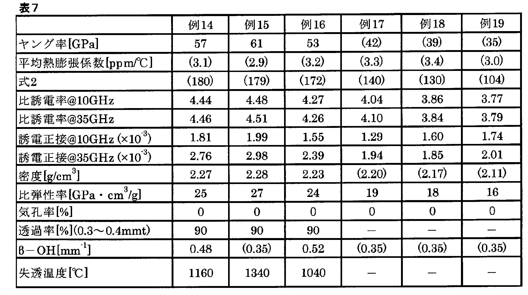

表5~8に示すように、本発明のガラス基板は、熱膨張率とヤング率との積(式2で表される値)が300以下と小さいため、急激な温度差が発生する場合においても引張り応力が発生しにくい。その結果、急激な温度変化が生じるような環境下での使用が、温度差が発生しやすい加工工程での破損を抑制することができる。
As shown in Tables 5 to 8, the glass substrate of the present invention has a small product of the coefficient of thermal expansion and Young's modulus (value expressed by Equation 2) as small as 300 or less. However, tensile stress is unlikely to occur. As a result, use in an environment in which a rapid temperature change occurs can suppress breakage in a machining process in which a temperature difference is likely to occur.
また、本発明のガラス基板は、20℃、35GHzでの比誘電率が10以下であり、かつ20℃、35GHzでの誘電正接が0.006以下であることにより、高周波領域での誘電損失が低減できる。
In addition, the glass substrate of the present invention has a relative dielectric constant of 10 or less at 20 ° C. and 35 GHz, and a dielectric loss tangent at 20 ° C. and 35 GHz of 0.006 or less. Can be reduced.
さらに、本発明のガラス基板を用いると、ビッカース硬度が小さいため、軽荷重で加工が可能であり、クラック発生荷重が大きいためマイクロクラックなどの欠点が発生しにくいため高強度の基板が得られる。
Furthermore, when the glass substrate of the present invention is used, since the Vickers hardness is small, it can be processed with a light load, and since the crack generation load is large, defects such as microcracks are unlikely to occur, so that a high strength substrate can be obtained.
本発明を特定の態様を参照して詳細に説明したが、本発明の精神と範囲を離れることなく様々な変更および修正が可能であることは、当業者にとって明らかである。なお、本出願は、2018年3月20日付けで出願された日本特許出願(特願2018-53082)に基づいており、その全体が引用により援用される。また、ここに引用されるすべての参照は全体として取り込まれる。
Although the present invention has been described in detail with reference to specific embodiments, it will be apparent to those skilled in the art that various changes and modifications can be made without departing from the spirit and scope of the invention. Note that this application is based on a Japanese patent application filed on March 20, 2018 (Japanese Patent Application No. 2018-53082), which is incorporated by reference in its entirety. Also, all references cited herein are incorporated as a whole.
本発明のガラス基板は、高周波信号の誘電損失性に優れており、高い耐熱衝撃性を示す。そのため、当該ガラス基板を用いた回路基板は、高周波信号の伝送損失性に優れ、またレーザー等の熱を用いた加工性にも優れている。
The glass substrate of the present invention is excellent in high-frequency signal dielectric loss and exhibits high thermal shock resistance. Therefore, a circuit board using the glass substrate is excellent in high-frequency signal transmission loss and excellent in workability using heat such as laser.
このようなガラス基板および回路基板は、10GHzを超えるような高周波信号、特に30GHzを超える高周波信号、さらには35GHz以上の高周波信号を扱う高周波電子デバイス全般や、温度変化の大きい環境下で用いられる液晶アンテナ、レーザー等による穴開け加工を伴うデバイス等の部材として非常に有用である。
Such glass substrates and circuit boards are generally used for high-frequency electronic devices that handle high-frequency signals exceeding 10 GHz, particularly high-frequency signals exceeding 30 GHz, and further high-frequency signals of 35 GHz or higher, and liquid crystal used in environments with large temperature changes. It is very useful as a member for devices such as antennas, lasers, and the like that involve drilling.
1 回路基板
2 ガラス基板
2a 第1の主表面
2b 第2の主表面
3 第1の配線層
4 第2の配線層 DESCRIPTION OF SYMBOLS 1Circuit board 2 Glass substrate 2a 1st main surface 2b 2nd main surface 3 1st wiring layer 4 2nd wiring layer
2 ガラス基板
2a 第1の主表面
2b 第2の主表面
3 第1の配線層
4 第2の配線層 DESCRIPTION OF SYMBOLS 1
Claims (22)
- {ヤング率(GPa)×50~350℃における平均熱膨張係数(ppm/℃)}≦300(GPa・ppm/℃)の関係を満たし、
20℃、35GHzでの比誘電率が10以下であり、かつ
20℃、35GHzでの誘電正接が0.006以下であるガラス基板。 {Young's modulus (GPa) × average thermal expansion coefficient (ppm / ° C.) at 50 to 350 ° C.} ≦ 300 (GPa · ppm / ° C.)
A glass substrate having a relative dielectric constant of 10 or less at 20 ° C. and 35 GHz and a dielectric loss tangent of 0.006 or less at 20 ° C. and 35 GHz. - ヤング率が70GPa以下である請求項1に記載のガラス基板。 The glass substrate according to claim 1, wherein the Young's modulus is 70 GPa or less.
- 50~350℃における平均熱膨張係数が5ppm/℃以下である請求項1又は2に記載のガラス基板。 3. The glass substrate according to claim 1, wherein an average coefficient of thermal expansion at 50 to 350 ° C. is 5 ppm / ° C. or less.
- 20℃、10GHzでの比誘電率が10以下であり、かつ20℃、10GHzでの誘電正接が0.006以下である請求項1~3のいずれか1項に記載のガラス基板。 The glass substrate according to any one of claims 1 to 3, wherein a relative dielectric constant at 20 ° C and 10 GHz is 10 or less, and a dielectric loss tangent at 20 ° C and 10 GHz is 0.006 or less.
- 主面の面積が100~100000cm2であり、かつ厚さが0.01~2mmである請求項1~4のいずれか1項に記載のガラス基板。 The glass substrate according to any one of claims 1 to 4, wherein the main surface has an area of 100 to 100,000 cm 2 and a thickness of 0.01 to 2 mm.
- 端面の少なくとも一部が面取りされている請求項1~5のいずれか1項に記載のガラス基板。 The glass substrate according to any one of claims 1 to 5, wherein at least a part of the end surface is chamfered.
- ビッカース硬度が400~550である請求項1~6のいずれか1項に記載のガラス基板。 The glass substrate according to any one of claims 1 to 6, having a Vickers hardness of 400 to 550.
- クラック発生荷重が1.96N超である請求項1~7のいずれか1項に記載のガラス基板。 The glass substrate according to any one of claims 1 to 7, wherein a crack generation load is more than 1.96N.
- 密度が2.5g/cm3以下である請求項1~8のいずれか1項に記載のガラス基板。 The glass substrate according to any one of claims 1 to 8, wherein the density is 2.5 g / cm 3 or less.
- 主面の表面の少なくとも一部に圧縮応力層を有する請求項1~9のいずれか1項に記載のガラス基板。 The glass substrate according to any one of claims 1 to 9, which has a compressive stress layer on at least a part of the surface of the main surface.
- 気孔率が0.1%以下である請求項1~10のいずれか1項に記載のガラス基板。 The glass substrate according to any one of claims 1 to 10, which has a porosity of 0.1% or less.
- 波長350nmの光の透過率が50%以上である請求項1~11のいずれか1項に記載のガラス基板。 The glass substrate according to any one of claims 1 to 11, wherein the transmittance of light having a wavelength of 350 nm is 50% or more.
- β-OH値が0.05~0.8mm-1である請求項1~12のいずれか1項に記載のガラス基板。 The glass substrate according to any one of claims 1 to 12, which has a β-OH value of 0.05 to 0.8 mm -1 .
- SiO2を主成分とし、
酸化物基準のモル百分率表示で、
Al2O3及びB2O3を合計で1~40%含有し、
{Al2O3/(Al2O3+B2O3)}で表される含有量のモル比が0~0.45であり、かつ
アルカリ土類金属酸化物を合計で0.1~13%含有する、請求項1~13のいずれか1項に記載のガラス基板。 Mainly composed of SiO 2
In mole percentage display on oxide basis,
Al 2 O 3 and B 2 O 3 are contained 1 to 40% in total,
The molar ratio of the content represented by {Al 2 O 3 / (Al 2 O 3 + B 2 O 3 )} is 0 to 0.45, and the total number of alkaline earth metal oxides is 0.1 to 13 The glass substrate according to any one of claims 1 to 13, wherein the glass substrate is contained. - 酸化物基準のモル百分率表示で、アルカリ金属酸化物を合計で0.001~5%含有する請求項1~14のいずれか1項に記載のガラス基板。 The glass substrate according to any one of claims 1 to 14, which contains a total of 0.001 to 5% of alkali metal oxides in terms of oxide-based mole percentage.
- 前記アルカリ金属酸化物のうち、{Na2O/(Na2O+K2O)}で表される含有量のモル比が0.01~0.99である請求項15に記載のガラス基板。 The glass substrate according to claim 15, wherein the molar ratio of the content represented by {Na 2 O / (Na 2 O + K 2 O)} in the alkali metal oxide is 0.01 to 0.99.
- 酸化物基準のモル百分率表示での含有量が
(1.02×SiO2+3.42×Al2O3+0.74×B2O3+9.17×MgO+12.55×CaO+13.85×SrO+14.44×BaO+31.61×Na2O+20.35×K2O)≦300の関係を満たす請求項1~16のいずれか1項に記載のガラス基板。 Content in terms of mole percentage on the basis of oxide is (1.02 × SiO 2 + 3.42 × Al 2 O 3 + 0.74 × B 2 O 3 + 9.17 × MgO + 12.55 × CaO + 13.85 × SrO + 14.44 The glass substrate according to any one of claims 1 to 16, which satisfies a relationship of × BaO + 31.61 × Na 2 O + 20.35 × K 2 O) ≦ 300. - 酸化物基準のモル百分率表示で、Al2O3を0~10%及びB2O3を9~30%含有する請求項1~17のいずれか1項に記載のガラス基板。 The glass substrate according to any one of claims 1 to 17, which contains 0 to 10% Al 2 O 3 and 9 to 30% B 2 O 3 in terms of a molar percentage based on oxide.
- 酸化物基準のモル百分率表示で、FeをFe2O3換算で0~0.012%含有する請求項1~18のいずれか1項に記載のガラス基板。 The glass substrate according to any one of claims 1 to 18, which contains 0 to 0.012% of Fe in terms of Fe 2 O 3 in terms of mole percentage based on oxide.
- 液晶アンテナ又は高周波回路に用いられる請求項1~19のいずれか1項に記載のガラス基板。 The glass substrate according to any one of claims 1 to 19, which is used for a liquid crystal antenna or a high-frequency circuit.
- 請求項1~19のいずれか1項に記載のガラス基板を有する液晶アンテナ。 A liquid crystal antenna having the glass substrate according to any one of claims 1 to 19.
- 請求項1~19のいずれか1項に記載のガラス基板を有する高周波デバイス。 A high frequency device having the glass substrate according to any one of claims 1 to 19.
Priority Applications (7)
| Application Number | Priority Date | Filing Date | Title |
|---|---|---|---|
| KR1020207026692A KR20200133340A (en) | 2018-03-20 | 2019-03-13 | Glass substrate, liquid crystal antenna and high frequency device |
| CN201980020056.4A CN111886209A (en) | 2018-03-20 | 2019-03-13 | Glass substrate, liquid crystal antenna, and high-frequency device |
| JP2020508282A JPWO2019181707A1 (en) | 2018-03-20 | 2019-03-13 | Glass substrate, LCD antenna and high frequency device |
| EP19771064.3A EP3770129B1 (en) | 2018-03-20 | 2019-03-13 | Glass substrate, liquid crystal antenna and high-frequency device |
| US17/022,365 US11239549B2 (en) | 2018-03-20 | 2020-09-16 | Glass substrate, liquid crystal antenna and high-frequency device |
| US17/550,080 US11594811B2 (en) | 2018-03-20 | 2021-12-14 | Glass substrate, liquid crystal antenna and high-frequency device |
| US18/157,213 US20230163453A1 (en) | 2018-03-20 | 2023-01-20 | Glass substrate, liquid crystal antenna and high-frequency device |
Applications Claiming Priority (2)
| Application Number | Priority Date | Filing Date | Title |
|---|---|---|---|
| JP2018053082 | 2018-03-20 | ||
| JP2018-053082 | 2018-03-20 |
Related Child Applications (1)
| Application Number | Title | Priority Date | Filing Date |
|---|---|---|---|
| US17/022,365 Continuation US11239549B2 (en) | 2018-03-20 | 2020-09-16 | Glass substrate, liquid crystal antenna and high-frequency device |
Publications (1)
| Publication Number | Publication Date |
|---|---|
| WO2019181707A1 true WO2019181707A1 (en) | 2019-09-26 |
Family
ID=67987307
Family Applications (1)
| Application Number | Title | Priority Date | Filing Date |
|---|---|---|---|
| PCT/JP2019/010424 WO2019181707A1 (en) | 2018-03-20 | 2019-03-13 | Glass substrate, liquid crystal antenna and high-frequency device |
Country Status (7)
| Country | Link |
|---|---|
| US (3) | US11239549B2 (en) |
| EP (1) | EP3770129B1 (en) |
| JP (1) | JPWO2019181707A1 (en) |
| KR (1) | KR20200133340A (en) |
| CN (1) | CN111886209A (en) |
| TW (2) | TWI806992B (en) |
| WO (1) | WO2019181707A1 (en) |
Cited By (6)
| Publication number | Priority date | Publication date | Assignee | Title |
|---|---|---|---|---|
| CN111628263A (en) * | 2020-06-04 | 2020-09-04 | 上海航天电子通讯设备研究所 | LCP-based multi-layer rectangular three-dimensional micro waveguide manufacturing method and micro waveguide |
| US11168018B2 (en) | 2013-08-15 | 2021-11-09 | Corning Incorporated | Aluminoborosilicate glass substantially free of alkali oxides |
| WO2022054694A1 (en) * | 2020-09-08 | 2022-03-17 | 日本電気硝子株式会社 | Glass, and method for measuring dielectric properties using same |
| USRE49307E1 (en) | 2013-08-15 | 2022-11-22 | Corning Incorporated | Alkali-doped and alkali-free boroaluminosilicate glass |
| US20230051724A1 (en) * | 2020-01-03 | 2023-02-16 | Corning Incorporated | Strengthened glass articles and consumer electronic products including the same |
| CN117147321A (en) * | 2023-10-30 | 2023-12-01 | 新疆泰齐石油科技有限公司 | Method and device for representing crack morphology of experimental rock sample |
Families Citing this family (4)
| Publication number | Priority date | Publication date | Assignee | Title |
|---|---|---|---|---|
| CN112759255A (en) * | 2016-09-13 | 2021-05-07 | Agc株式会社 | Glass substrate for high-frequency device and circuit substrate for high-frequency device |
| JP2022522986A (en) * | 2019-01-18 | 2022-04-21 | コーニング インコーポレイテッド | Low dielectric loss glass for electronic devices |
| EP3787115A1 (en) * | 2019-08-30 | 2021-03-03 | Nokia Solutions and Networks Oy | Device for analogue and programmable computing operation on electromagnetic waves and method of operating the same |
| CN113277730B (en) * | 2021-06-21 | 2022-04-15 | 成都光明光电有限责任公司 | Low dielectric constant glass composition |
Citations (11)
| Publication number | Priority date | Publication date | Assignee | Title |
|---|---|---|---|---|
| JP2004244271A (en) | 2003-02-14 | 2004-09-02 | Asahi Glass Co Ltd | Lead-free glass, composition for electronic circuit board, and electronic circuit board |
| JP2010030848A (en) * | 2008-07-30 | 2010-02-12 | Ohara Inc | Glass |
| JP2013077769A (en) | 2011-09-30 | 2013-04-25 | Nippon Zeon Co Ltd | Circuit board |
| JP2014504250A (en) * | 2010-11-30 | 2014-02-20 | コーニング インコーポレイテッド | Alkaline earth aluminoborosilicate crack resistant glass |
| JP2015512852A (en) * | 2012-02-29 | 2015-04-30 | コーニング インコーポレイテッド | Low CTE alkali-free boroaluminosilicate glass composition and glass article comprising the same |
| JP2016528152A (en) * | 2013-08-15 | 2016-09-15 | コーニング インコーポレイテッド | Alkali-doped and alkali-free boroaluminosilicate glass |
| JP2016209987A (en) * | 2015-05-13 | 2016-12-15 | 信越化学工業株式会社 | Manufacturing method of substrate |
| JP2017506467A (en) | 2014-02-19 | 2017-03-02 | カイメタ コーポレイション | Dynamic polarization and coupling control for movable multilayer cylindrical feed holographic antenna |
| JP2017506471A (en) | 2014-02-19 | 2017-03-02 | カイメタ コーポレイション | Dynamic polarization and coupling control for a moving cylindrical feed holographic antenna |
| WO2018051793A1 (en) * | 2016-09-13 | 2018-03-22 | 旭硝子株式会社 | Glass substrate for high frequency device and circuit board for high frequency device |
| JP2018053082A (en) | 2016-09-28 | 2018-04-05 | 富士ゼロックス株式会社 | Resin composition, and resin molded body |
Family Cites Families (17)
| Publication number | Priority date | Publication date | Assignee | Title |
|---|---|---|---|---|
| JP3240271B2 (en) * | 1996-02-29 | 2001-12-17 | ティーディーケイ株式会社 | Ceramic substrate |
| JP4704585B2 (en) * | 2000-07-07 | 2011-06-15 | 株式会社オハラ | Low expansion transparent crystallized glass, crystallized glass substrate and optical waveguide device |
| EP1443029A4 (en) * | 2001-11-05 | 2007-08-01 | Asahi Glass Co Ltd | Glass ceramic composition |
| DE10238607B4 (en) * | 2002-08-16 | 2006-04-27 | Schott Ag | Method for shaping glass or glass ceramic and its use |
| CN1720136A (en) * | 2002-12-05 | 2006-01-11 | 株式会社钟化 | Laminate, printed wiring board and method for manufacturing them |
| CN100579333C (en) * | 2003-01-23 | 2010-01-06 | 东丽株式会社 | The manufacture method of member for circuit board, circuit substrate and the manufacturing installation of circuit substrate |
| CN101033114A (en) * | 2007-02-12 | 2007-09-12 | 洛玻集团洛阳晶纬玻璃纤维有限公司 | Glass with low dielectric constant |
| CN102200612A (en) * | 2011-04-27 | 2011-09-28 | 中国科学院微电子研究所 | Optical-fibre-embedded glass plate and manufacturing method thereof |
| CN102923953A (en) * | 2012-11-20 | 2013-02-13 | 蚌埠玻璃工业设计研究院 | Low dielectric constant glass plate and preparation method thereof |
| US10211169B2 (en) * | 2014-05-27 | 2019-02-19 | University Of Florida Research Foundation, Inc. | Glass interposer integrated high quality electronic components and systems |
| CN107074622A (en) * | 2014-10-23 | 2017-08-18 | 旭硝子株式会社 | alkali-free glass |
| KR20230148860A (en) * | 2014-11-28 | 2023-10-25 | 에이지씨 가부시키가이샤 | Liquid crystal display panel |
| MY186276A (en) | 2015-05-13 | 2021-07-02 | Shinetsu Chemical Co | Method for producing substrates |
| JP6288347B2 (en) * | 2016-04-22 | 2018-03-07 | 旭硝子株式会社 | Glass substrate for display |
| WO2018038059A1 (en) * | 2016-08-23 | 2018-03-01 | 旭硝子株式会社 | Alkali-free glass |
| CN106810286B (en) * | 2017-01-19 | 2020-03-10 | 哈尔滨工业大学 | Boron nitride fiber reinforced cordierite ceramic matrix composite and preparation method thereof |
| CN106904953B (en) * | 2017-03-24 | 2021-01-01 | 电子科技大学 | High-thermal-expansion-coefficient ceramic material for high-density packaging and preparation method thereof |
-
2019
- 2019-03-13 CN CN201980020056.4A patent/CN111886209A/en active Pending
- 2019-03-13 KR KR1020207026692A patent/KR20200133340A/en not_active Application Discontinuation
- 2019-03-13 EP EP19771064.3A patent/EP3770129B1/en active Active
- 2019-03-13 JP JP2020508282A patent/JPWO2019181707A1/en active Pending
- 2019-03-13 WO PCT/JP2019/010424 patent/WO2019181707A1/en unknown
- 2019-03-18 TW TW108109062A patent/TWI806992B/en active
- 2019-03-18 TW TW112120599A patent/TW202337854A/en unknown
-
2020
- 2020-09-16 US US17/022,365 patent/US11239549B2/en active Active
-
2021
- 2021-12-14 US US17/550,080 patent/US11594811B2/en active Active
-
2023
- 2023-01-20 US US18/157,213 patent/US20230163453A1/en active Pending
Patent Citations (11)
| Publication number | Priority date | Publication date | Assignee | Title |
|---|---|---|---|---|
| JP2004244271A (en) | 2003-02-14 | 2004-09-02 | Asahi Glass Co Ltd | Lead-free glass, composition for electronic circuit board, and electronic circuit board |
| JP2010030848A (en) * | 2008-07-30 | 2010-02-12 | Ohara Inc | Glass |
| JP2014504250A (en) * | 2010-11-30 | 2014-02-20 | コーニング インコーポレイテッド | Alkaline earth aluminoborosilicate crack resistant glass |
| JP2013077769A (en) | 2011-09-30 | 2013-04-25 | Nippon Zeon Co Ltd | Circuit board |
| JP2015512852A (en) * | 2012-02-29 | 2015-04-30 | コーニング インコーポレイテッド | Low CTE alkali-free boroaluminosilicate glass composition and glass article comprising the same |
| JP2016528152A (en) * | 2013-08-15 | 2016-09-15 | コーニング インコーポレイテッド | Alkali-doped and alkali-free boroaluminosilicate glass |
| JP2017506467A (en) | 2014-02-19 | 2017-03-02 | カイメタ コーポレイション | Dynamic polarization and coupling control for movable multilayer cylindrical feed holographic antenna |
| JP2017506471A (en) | 2014-02-19 | 2017-03-02 | カイメタ コーポレイション | Dynamic polarization and coupling control for a moving cylindrical feed holographic antenna |
| JP2016209987A (en) * | 2015-05-13 | 2016-12-15 | 信越化学工業株式会社 | Manufacturing method of substrate |
| WO2018051793A1 (en) * | 2016-09-13 | 2018-03-22 | 旭硝子株式会社 | Glass substrate for high frequency device and circuit board for high frequency device |
| JP2018053082A (en) | 2016-09-28 | 2018-04-05 | 富士ゼロックス株式会社 | Resin composition, and resin molded body |
Cited By (7)
| Publication number | Priority date | Publication date | Assignee | Title |
|---|---|---|---|---|
| US11168018B2 (en) | 2013-08-15 | 2021-11-09 | Corning Incorporated | Aluminoborosilicate glass substantially free of alkali oxides |
| USRE49307E1 (en) | 2013-08-15 | 2022-11-22 | Corning Incorporated | Alkali-doped and alkali-free boroaluminosilicate glass |
| US20230051724A1 (en) * | 2020-01-03 | 2023-02-16 | Corning Incorporated | Strengthened glass articles and consumer electronic products including the same |
| CN111628263A (en) * | 2020-06-04 | 2020-09-04 | 上海航天电子通讯设备研究所 | LCP-based multi-layer rectangular three-dimensional micro waveguide manufacturing method and micro waveguide |
| WO2022054694A1 (en) * | 2020-09-08 | 2022-03-17 | 日本電気硝子株式会社 | Glass, and method for measuring dielectric properties using same |
| CN117147321A (en) * | 2023-10-30 | 2023-12-01 | 新疆泰齐石油科技有限公司 | Method and device for representing crack morphology of experimental rock sample |
| CN117147321B (en) * | 2023-10-30 | 2024-02-20 | 新疆泰齐石油科技有限公司 | Method and device for representing crack morphology of experimental rock sample |
Also Published As
| Publication number | Publication date |
|---|---|
| TW201940445A (en) | 2019-10-16 |
| EP3770129A1 (en) | 2021-01-27 |
| US20220102850A1 (en) | 2022-03-31 |
| US11594811B2 (en) | 2023-02-28 |
| US20230163453A1 (en) | 2023-05-25 |
| TWI806992B (en) | 2023-07-01 |
| US20210013598A1 (en) | 2021-01-14 |
| JPWO2019181707A1 (en) | 2021-03-25 |
| TW202337854A (en) | 2023-10-01 |
| EP3770129B1 (en) | 2023-07-12 |
| US11239549B2 (en) | 2022-02-01 |
| EP3770129A4 (en) | 2021-12-29 |
| KR20200133340A (en) | 2020-11-27 |
| CN111886209A (en) | 2020-11-03 |
Similar Documents
| Publication | Publication Date | Title |
|---|---|---|
| WO2019181707A1 (en) | Glass substrate, liquid crystal antenna and high-frequency device | |
| JP7415237B2 (en) | Glass substrates for high frequency devices and circuit boards for high frequency devices | |
| WO2019181706A1 (en) | Substrate, liquid crystal antenna and high-frequency device | |
| JP7409316B2 (en) | Glass substrates for high frequency devices, liquid crystal antennas and high frequency devices | |
| WO2023219023A1 (en) | Glass, glass sheet, and method for producing glass sheet | |
| EP4206153A1 (en) | Alkali-free glass and glass plate | |
| TW202406869A (en) | Glass, glass sheets and methods of manufacturing glass sheets |
Legal Events
| Date | Code | Title | Description |
|---|---|---|---|
| 121 | Ep: the epo has been informed by wipo that ep was designated in this application |
Ref document number: 19771064 Country of ref document: EP Kind code of ref document: A1 |
|
| ENP | Entry into the national phase |
Ref document number: 2020508282 Country of ref document: JP Kind code of ref document: A |
|
| NENP | Non-entry into the national phase |
Ref country code: DE |
|
| ENP | Entry into the national phase |
Ref document number: 2019771064 Country of ref document: EP Effective date: 20201020 |