WO2019156177A1 - Optical wavelength converter and method for manufacturing optical wavelength converter - Google Patents
Optical wavelength converter and method for manufacturing optical wavelength converter Download PDFInfo
- Publication number
- WO2019156177A1 WO2019156177A1 PCT/JP2019/004461 JP2019004461W WO2019156177A1 WO 2019156177 A1 WO2019156177 A1 WO 2019156177A1 JP 2019004461 W JP2019004461 W JP 2019004461W WO 2019156177 A1 WO2019156177 A1 WO 2019156177A1
- Authority
- WO
- WIPO (PCT)
- Prior art keywords
- substrate
- region
- laser beam
- wavelength
- virtual axis
- Prior art date
Links
Images


Classifications
-
- G—PHYSICS
- G02—OPTICS
- G02F—OPTICAL DEVICES OR ARRANGEMENTS FOR THE CONTROL OF LIGHT BY MODIFICATION OF THE OPTICAL PROPERTIES OF THE MEDIA OF THE ELEMENTS INVOLVED THEREIN; NON-LINEAR OPTICS; FREQUENCY-CHANGING OF LIGHT; OPTICAL LOGIC ELEMENTS; OPTICAL ANALOGUE/DIGITAL CONVERTERS
- G02F1/00—Devices or arrangements for the control of the intensity, colour, phase, polarisation or direction of light arriving from an independent light source, e.g. switching, gating or modulating; Non-linear optics
- G02F1/35—Non-linear optics
- G02F1/37—Non-linear optics for second-harmonic generation
- G02F1/377—Non-linear optics for second-harmonic generation in an optical waveguide structure
- G02F1/383—Non-linear optics for second-harmonic generation in an optical waveguide structure of the optical fibre type
-
- G—PHYSICS
- G02—OPTICS
- G02F—OPTICAL DEVICES OR ARRANGEMENTS FOR THE CONTROL OF LIGHT BY MODIFICATION OF THE OPTICAL PROPERTIES OF THE MEDIA OF THE ELEMENTS INVOLVED THEREIN; NON-LINEAR OPTICS; FREQUENCY-CHANGING OF LIGHT; OPTICAL LOGIC ELEMENTS; OPTICAL ANALOGUE/DIGITAL CONVERTERS
- G02F1/00—Devices or arrangements for the control of the intensity, colour, phase, polarisation or direction of light arriving from an independent light source, e.g. switching, gating or modulating; Non-linear optics
- G02F1/35—Non-linear optics
- G02F1/353—Frequency conversion, i.e. wherein a light beam is generated with frequency components different from those of the incident light beams
- G02F1/3544—Particular phase matching techniques
- G02F1/3548—Quasi phase matching [QPM], e.g. using a periodic domain inverted structure
-
- G—PHYSICS
- G02—OPTICS
- G02F—OPTICAL DEVICES OR ARRANGEMENTS FOR THE CONTROL OF LIGHT BY MODIFICATION OF THE OPTICAL PROPERTIES OF THE MEDIA OF THE ELEMENTS INVOLVED THEREIN; NON-LINEAR OPTICS; FREQUENCY-CHANGING OF LIGHT; OPTICAL LOGIC ELEMENTS; OPTICAL ANALOGUE/DIGITAL CONVERTERS
- G02F1/00—Devices or arrangements for the control of the intensity, colour, phase, polarisation or direction of light arriving from an independent light source, e.g. switching, gating or modulating; Non-linear optics
- G02F1/35—Non-linear optics
- G02F1/355—Non-linear optics characterised by the materials used
- G02F1/3551—Crystals
-
- G—PHYSICS
- G02—OPTICS
- G02F—OPTICAL DEVICES OR ARRANGEMENTS FOR THE CONTROL OF LIGHT BY MODIFICATION OF THE OPTICAL PROPERTIES OF THE MEDIA OF THE ELEMENTS INVOLVED THEREIN; NON-LINEAR OPTICS; FREQUENCY-CHANGING OF LIGHT; OPTICAL LOGIC ELEMENTS; OPTICAL ANALOGUE/DIGITAL CONVERTERS
- G02F1/00—Devices or arrangements for the control of the intensity, colour, phase, polarisation or direction of light arriving from an independent light source, e.g. switching, gating or modulating; Non-linear optics
- G02F1/35—Non-linear optics
- G02F1/355—Non-linear optics characterised by the materials used
- G02F1/3555—Glasses
-
- G—PHYSICS
- G02—OPTICS
- G02F—OPTICAL DEVICES OR ARRANGEMENTS FOR THE CONTROL OF LIGHT BY MODIFICATION OF THE OPTICAL PROPERTIES OF THE MEDIA OF THE ELEMENTS INVOLVED THEREIN; NON-LINEAR OPTICS; FREQUENCY-CHANGING OF LIGHT; OPTICAL LOGIC ELEMENTS; OPTICAL ANALOGUE/DIGITAL CONVERTERS
- G02F1/00—Devices or arrangements for the control of the intensity, colour, phase, polarisation or direction of light arriving from an independent light source, e.g. switching, gating or modulating; Non-linear optics
- G02F1/35—Non-linear optics
- G02F1/37—Non-linear optics for second-harmonic generation
- G02F1/377—Non-linear optics for second-harmonic generation in an optical waveguide structure
Definitions
- the present disclosure relates to a wavelength conversion optical device and a method for manufacturing the wavelength conversion optical device.
- Materials used for optical devices utilizing second-order nonlinear optical phenomena include LiNbO 3 (LN) crystal, KTiOPO 4 (KTP) crystal, LiB 3 O 5 (LBO) crystal, or ⁇ -BaB 2 O 4 (BBO).
- Ferroelectric optical crystals such as crystals are the mainstream.
- Optical devices using these crystals have been developed in a wide range of application fields based on wavelength conversion. For example, in the laser processing field, optical devices using these crystals are used for shortening the wavelength by second harmonic generation (SHG) of an optical fiber laser. Since the beam spot diameter can be reduced, such an optical device enables fine processing.
- SHG second harmonic generation
- optical devices using these crystals are capable of batch multiplexing conversion from a C-band WDM signal to an L-band ( It is used as a wavelength conversion optical device that performs simultaneous wavelength conversion.
- terahertz spectroscopy capable of observing intermolecular vibrations caused by hydrogen bonds or the like has attracted attention, and optical devices using these crystals are used as light sources for generating the terahertz light.
- compound semiconductor crystals such as GaAs, GaP, GaN, CdTe, ZnSe, ZnO, and the like have also been used as materials for optical devices utilizing the second-order nonlinear optical phenomenon.
- these materials have a remarkable progress in the fabrication technology of periodic-poled structures essential for second-order nonlinear optical devices. It is attracting attention as a material.
- the wavelength conversion method can be classified into angle phase matching (angle phase matching) and quasi phase matching (QPM: Quasi Phase matching) by periodic polarization inversion.
- the quasi-phase matching enables generation of various phase matching wavelengths by appropriately designing the periodical polarization inversion width (poling pitch), and enables wavelength conversion in all the transparent regions of the material.
- Pseudo phase matching does not have a walk-off angle due to angular phase matching, so that the beam quality is good and the interaction length can be increased, making it suitable for increasing efficiency and suppressing coupling loss. Therefore, it is an effective method in processing and measurement.
- the wavelength conversion optical device of the present disclosure includes a crystalline or amorphous substrate, a plurality of first crystal regions each having a radial first polarization order structure, and a plurality of each having a radial second polarization order structure.
- a second crystal region When the substrate is viewed from a reference direction orthogonal to a certain virtual axis set in the substrate, a first region and a second region that are directly adjacent to each other with the virtual axis interposed therebetween are defined.
- the radiation center of the first polarization ordered structure is arranged along the virtual axis in the first region of the substrate. When the substrate is viewed from the reference direction, each of the plurality of first crystal regions protrudes into the second region across the virtual axis.
- the radiation center of the second polarization ordered structure is disposed along the virtual axis in the second region of the substrate, and the radiation center of the second polarization ordered structure alternates with the radiation center of the first polarization ordered structure along the virtual axis.
- the radiation center of the second polarization ordered structure has been placed.
- each of the plurality of second crystal regions protrudes into the first region across the virtual axis.
- the method for manufacturing a wavelength conversion optical device includes a pre-process for preparing a substrate, a plurality of first crystal regions each having a radial first polarization order structure, and a plurality of first crystal structures each having a radial second polarization order structure.
- the substrate is made of crystalline or amorphous. Further, when the substrate is viewed from a reference direction orthogonal to a certain virtual axis set in the substrate, a first region and a second region that are directly adjacent to each other with the virtual axis interposed therebetween are defined.
- Radiation centers in the first polarization ordered structure of the plurality of first crystal regions are arranged along the virtual axis in the first region of the substrate.
- each of the plurality of first crystal regions protrudes into the second region across the virtual axis.
- the radiation center in the second polarization ordered structure of the plurality of second crystal regions is arranged along the virtual axis in the second region of the substrate.
- the plurality of second crystal regions are arranged such that when the substrate is viewed from the reference direction, the radiation centers of the second polarization ordered structure are alternately arranged with the radiation centers of the first polarization ordered structure along the virtual axis.
- each part protrudes into the first region across the virtual axis.
- the first processing step includes a laser beam irradiation step, and the laser beam irradiation step includes a plurality of first condensing points and a plurality of second crystals corresponding to the radiation centers in the first polarization ordered structure of the plurality of first crystal regions.
- Laser light for forming the first and second polarization ordered structures is irradiated to each of the plurality of second condensing points corresponding to the emission centers in the second polarization ordered structure of the region.
- FIG. 1 are sectional drawings which show the structure of 1 A of wavelength conversion optical devices which concern on one Embodiment of this invention. These are the top views which expanded crystal area 10A, 10B. These are the flowcharts which show the manufacturing method of one Embodiment. These are figures which show a mode that the some condensing point P1 and the some condensing point P2 were set to the board
- FIG. These are the graphs which show an example of the light intensity distribution of the laser beam in one Embodiment.
- FIG. are sectional drawings which show the structure of the wavelength conversion optical device 1B which concerns on a 1st modification. These are graphs showing an example of the light intensity distribution of the laser light for forming the crystal regions 10A and 10B of the first modification.
- FIG. 10B is a sectional view taken along line IXb-IXb in FIG. 10A.
- FIG. 10B is a sectional view taken along line IXc-IXc in FIG. 10A.
- FIG. 6 is a schematic diagram for explaining a polarization direction in a crystal region formed using a laser beam having the light intensity distribution shown in FIG. 5. These are the schematic diagrams for demonstrating the polarization direction in the crystal region formed by the manufacturing method of the wavelength conversion optical device which concerns on a 5th modification.
- FIG. 3 is an optical microscope image showing a state after irradiating laser light from a CO 2 laser onto SrO—TiO 2 —SiO 2 glass.
- FIG. 14B is a partially enlarged view of FIG. 14A.
- FIG. 3 is an optical microscope image showing a state after irradiating laser light from a CO 2 laser onto SrO—TiO 2 —SiO 2 glass.
- FIG. 15B is a partially enlarged view of FIG. 15A.
- FIG. 3 is an optical microscope image showing a state after irradiating laser light from a CO 2 laser onto SrO—TiO 2 —SiO 2 glass.
- FIG. 16B is a partially enlarged view of FIG. 16A.
- Patent Document 1 describes a method of forming a polarization-ordered structure defined by a polarization orientation by irradiating a laser with an electric field applied.
- the polarization order structure for realizing quasi phase matching is fine, and the interval between the polarization order structures adjacent to each other is extremely short.
- the interval between the positive electrode and the negative electrode for applying an electric field is narrowed, there is a problem that the machining process is complicated in order to avoid dielectric breakdown when a high voltage is applied.
- the present disclosure has been made to solve such a problem, and a wavelength conversion optical device capable of forming a polarization ordered structure for realizing quasi phase matching by a simple method, and the wavelength conversion light
- An object of the present invention is to provide a device manufacturing method.
- a wavelength conversion optical device includes, as an aspect thereof, a substrate made of a crystalline material or an amorphous material, and a plurality of first crystal regions each having a radial first polarization ordered structure. And a plurality of second crystal regions each having a radial second polarization ordered structure.
- a substrate made of a crystalline material or an amorphous material
- first crystal regions each having a radial first polarization ordered structure.
- second crystal regions each having a radial second polarization ordered structure.
- each of the plurality of first crystal regions protrudes into the second region across the virtual axis.
- the radiation center of the second polarization ordered structure is disposed along the virtual axis in the second region of the substrate, and the radiation center of the second polarization ordered structure alternates with the radiation center of the first polarization ordered structure along the virtual axis.
- each of the plurality of second crystal regions protrudes into the first region across the virtual axis.
- each crystal region of the wavelength conversion optical device can be easily formed by irradiating the substrate with laser light having a wavelength included in the absorption wavelength of the substrate, or by forming a heat source on or inside the substrate. is there.
- the substrate preferably has a channel optical waveguide structure having a virtual axis as an optical axis.
- a channel optical waveguide structure can increase the light propagation efficiency on the virtual axis.
- the substrate preferably includes at least one of a Fresnoite crystal, BaO—TiO 2 —GeO 2 —SiO 2 glass, and SrO—TiO 2 —SiO 2 glass.
- the above-mentioned radial polarization ordered structure can be easily formed by laser light irradiation.
- the substrate includes at least one of BaO—TiO 2 —GeO 2 —SiO 2 glass and SrO—TiO 2 —SiO 2 glass, and further includes a lanthanoid-based additive as an additive.
- a lanthanoid-based additive as an additive.
- the manufacturing direction of the wavelength conversion optical device includes, as one aspect, a pre-process for preparing a substrate, and a plurality of first crystal regions each having a radial first polarization ordered structure, A first processing step of providing a plurality of second crystal regions each having a radial second polarization ordered structure on a substrate.
- the substrate is made of crystalline or amorphous. Further, when the substrate is viewed from a reference direction orthogonal to a certain virtual axis set in the substrate, a first region and a second region that are directly adjacent to each other with the virtual axis interposed therebetween are defined.
- Radiation centers in the first polarization ordered structure of the plurality of first crystal regions are arranged along the virtual axis in the first region of the substrate.
- each of the plurality of first crystal regions protrudes into the second region across the virtual axis.
- the radiation center in the second polarization ordered structure of the plurality of second crystal regions is arranged along the virtual axis in the second region of the substrate.
- the plurality of second crystal regions are arranged such that when the substrate is viewed from the reference direction, the radiation centers of the second polarization ordered structure are alternately arranged with the radiation centers of the first polarization ordered structure along the virtual axis.
- each part protrudes into the first region across the virtual axis.
- the first processing step includes a laser beam irradiation step.
- the laser beam irradiation step corresponds to each of the plurality of first condensing points corresponding to the radiation center in the first polarization order structure of the plurality of first crystal regions and to the radiation center in the second polarization order structure of the plurality of second crystal regions.
- Each of the plurality of second condensing points is irradiated with laser light for forming the first and second polarization ordered structures.
- Each crystal region of the wavelength conversion optical device can be easily formed by irradiating the substrate with laser light having a wavelength included in the absorption wavelength of the substrate, or by forming a heat source on or inside the substrate. That is, according to the manufacturing method, it is possible to form a polarization ordered structure for realizing quasi phase matching by a simple method.
- the laser light for forming the polarization ordered structure preferably has a wavelength included in the absorption wavelength band of the substrate.
- the substrate can be directly heated by laser light irradiation.
- the laser light for forming the polarization ordered structure includes the first laser light for generating the excited electron high-density region on the substrate surface or in the substrate, and the excited electron high-density region.
- the second laser beam for heating may be included.
- the laser beam irradiation step includes a plurality of first focusing points and a plurality of second focusing points in a state where the focusing region of the second laser beam overlaps the focusing region of the first laser beam.
- the first laser beam and the second laser beam are irradiated to each of the light spots.
- a heat source for forming the polarization ordered structure can be formed at any position on the substrate surface or inside.
- the first laser beam has a wavelength that is out of the absorption wavelength band of the substrate or a wavelength at which the amount of light absorption to the substrate can be kept low, and fs (femtosecond) with a pulse width of less than 1 ps. It is preferable to include a laser beam.
- the second laser light has a wavelength that is out of the absorption wavelength band of the substrate in a region other than the condensing region of the first laser light or a wavelength that can suppress light absorption to the substrate low.
- a pulse laser beam having a pulse width of 1 ps or more, preferably 1 ns or more is preferably included.
- the second laser light has a wavelength outside the absorption wavelength band of the substrate in a region other than the light condensing region of the first laser light, or a wavelength that can suppress the amount of light absorption to the substrate low.
- Continuous (Wave) Laser light may be included.
- the condensing region of the first laser light means a region where excited electrons centered on the condensing point of the first laser light are generated at a high density (excited electron high density region).
- the number density is defined as a region of 10 19 / cm 3 or more.
- a state where the light condensing region of the first laser light and the light condensing region of the second laser light overlap (hereinafter referred to as an overlap state) is a point where the light condensing point of the first laser light and the second laser light are collected.
- the state where the condensing point is not coincident is also included.
- the overlapped state is in the excited state.
- the first laser light fs laser light
- the region where the fs laser light is condensed temporarily has a high density of excited electrons. Will occur.
- the second laser light pulse laser light or CW
- the second laser light pulse laser light or CW
- the laser beam is irradiated, light absorption can be preferentially and selectively induced only in the local region of the high density region of excited electrons.
- heat is generated in the light absorption region (the condensing region where the first and second laser beams overlap), and a crystal region is formed.
- High-efficiency wavelength conversion optical devices in various forms such as bulk shape and fiber shape by three-dimensionally scanning the overlapped condensing region of the first and second laser beams on the surface or inside of the substrate Can be realized.
- the manufacturing method may further include a second processing step of forming a channel optical waveguide structure with the virtual axis as the optical axis on the substrate before or after the laser light irradiation step. Good. Thereby, the light propagation efficiency on a virtual axis line can be improved.
- the channel optical waveguide structure is preferably formed by a dicing saw or dry etching. This makes it possible to easily form a channel optical waveguide structure on a crystalline or amorphous substrate.
- the laser light irradiation step it is preferable to irradiate the substrate with the laser light through an optical component for shaping the light intensity distribution of the laser light into a top hat shape.
- the optical component preferably includes a diffractive optical element or an aspheric lens. This makes it possible to easily generate laser light having a top hat-like light intensity distribution.
- the laser light source may include a CO 2 laser.
- the laser beam in the infrared region included in the absorption wavelength of many substrates can be irradiated to the substrate with a relatively large light intensity.
- the laser light irradiation step may irradiate the substrate with laser light in a state where a light absorbing material is disposed on the surface of the substrate.
- a light absorbing material is disposed on the surface of the substrate.
- the light absorbing material is preferably a carbon paste.
- each aspect listed in this [Description of Embodiments of the Invention] is applicable to each of all the remaining aspects or to all combinations of these remaining aspects. .
- FIG. 1 is a cross-sectional view illustrating a structure of a wavelength conversion optical device 1A according to an embodiment of the present disclosure, and illustrates a cross section of the wavelength conversion optical device 1A along the optical waveguide direction D1.
- the wavelength conversion optical device 1A according to the present embodiment includes a substrate 2 made of crystalline or amorphous.
- substrate 2 is a board
- the end faces 2a and 2b are orthogonal to the optical waveguide direction D1 and are parallel to each other.
- the substrate 2 has a property of transmitting at least light having a predetermined wavelength.
- the predetermined wavelength is, for example, a wavelength within a range of 400 nm to 4500 nm.
- the constituent material of the substrate 2 includes, for example, at least one of a Fresnoite crystal, BaO—TiO 2 —GeO 2 —SiO 2 glass, and SrO—TiO 2 —SiO 2 glass.
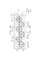
- the substrate 2 has a plurality of crystal regions 10A (planar shape when viewed from the reference direction orthogonal to the optical waveguide direction D1 (substantially the shape defined on the surface of the substrate 2) is an annular shape.
- FIG. 2 is an enlarged plan view of the crystal regions 10A and 10B.
- Crystal regions 10A and 10B are regions each having a radial polarization ordered structure.
- a polarization-ordered structure refers to a structure in which spontaneous polarization is oriented in a certain manner.
- the crystal region 10A of the present embodiment has a radial polarization ordered structure in which the spontaneous polarization A1 extends in the radial direction from the radiation center O1 toward the outer periphery of the crystal region 10A.
- the crystal region 10B of the present embodiment has a radial polarization order structure in which the spontaneous polarization A2 extends in the radial direction from the radiation center O2 toward the outer periphery of the crystal region 10B.
- this polarization ordered structure is formed by irradiating the substrate 2 with, for example, infrared laser light.
- the substrate 2 When the substrate 2 includes at least one of BaO—TiO 2 —GeO 2 —SiO 2 based glass and SrO—TiO 2 —SiO 2 based glass, the substrate 2 enhances absorption of laser light having a specific wavelength in the infrared region. Therefore, a metal contained in any group of lanthanoids, actinides, groups 4 to 12 may be included as an additive. Examples of lanthanoid-based or actinoid-based metals include Yb, Tm, and Er. Examples of the Group 4 to Group 12 metals include Ti, Cr, and Zn.
- the substrate 2 has a pair of regions 2c and 2d that sandwich a certain virtual axis AX set in the substrate 2.
- the pair of regions 2c and 2d are regions that are directly adjacent to each other with the virtual axis line sandwiched when the substrate 2 is viewed from a reference direction orthogonal to the virtual axis line.
- the emission centers (corresponding to the emission centers of the polarization-ordered structure) O1 of the plurality of crystal regions 10A are located in one of the regions 2c and are arranged in a line at equal intervals along the virtual axis AX.
- the radiation centers (corresponding to the radiation centers of the polarization-ordered structure) O2 of the plurality of crystal regions 10B are located in the other region 2d and are arranged in a line at equal intervals along the virtual axis AX. Furthermore, the radiation centers O1 of the plurality of crystal regions 10A and the radiation centers O2 of the plurality of crystal regions 10B are alternately arranged along the extending direction of the virtual axis AX (that is, the optical waveguide direction D1). In other words, when the surface of the substrate 2 is viewed from the direction D2 intersecting the extending direction of the virtual axis AX, the radiation centers O1 and the radiation centers O2 are alternately arranged on the surface of the substrate 2.
- a straight line connecting the radiation center O1 and the radiation center O2 adjacent to each other and the virtual axis AX intersect with each other at an angle greater than 0 ° and less than 90 °. Furthermore, the first straight line connecting the plurality of radiation centers O1 and the second straight line connecting the plurality of radiation centers O2 are each parallel to the virtual axis AX.
- the virtual axis AX is located between the first and second straight lines. That is, the distances between the plurality of radiation centers O1 and the virtual axis AX are equal, and the distances between the plurality of radiation centers O2 and the virtual axis AX are equal.
- the distance between the radiation center O1 and the virtual axis AX and the distance between the radiation center O2 and the virtual axis AX are equal to each other.
- the axis corresponding to the virtual axis AX (the line defined by the surface of the substrate 2) connects the midpoints of the line segments connecting the radiation centers O1 and O2 adjacent to each other on the surface of the substrate 2. It is parallel to the straight line.
- Each crystal region 10A partially protrudes to the region 2d side across the virtual axis AX. That is, each crystal region 10A has a portion that overlaps the virtual axis AX.
- Each crystal region 10B partially protrudes to the region 2c side across the virtual axis AX. That is, each crystal region 10B has a portion that overlaps the virtual axis AX.
- the crystal regions 10A and the crystal regions 10B are alternately arranged.
- the substrate 2 further has perforations (laser processing marks) 12A inside each crystal region 10A.
- the planar shape of the perforations 12A (the shape defined on the surface of the substrate 2) is a circle centered on the radiation center O1.
- the outer periphery of the perforation 12A is in contact with the inner periphery of the crystal region 10A.
- the substrate 2 further has perforations (laser processing marks) 12B inside each crystal region 10B.
- the planar shape of the perforation 12B is a circle centered on the radiation center O2.
- the outer periphery of the perforations 12B is in contact with the inner periphery of the crystal region 10B.
- These perforations 12 ⁇ / b> A and 12 ⁇ / b> B are holes (recesses or holes) generated when a part of the substrate 2 is melted by irradiation with laser light.
- the wavelength conversion region B1 is formed inside the substrate 2.
- the wavelength conversion region B1 is an optical waveguide that extends along the optical waveguide direction D1 with the virtual axis AX as an optical axis.
- One end B1a of the wavelength conversion region B1 reaches the end surface 2a of the substrate 2, and the other end B1b of the wavelength conversion region B1 reaches the end surface 2b of the substrate 2.
- the light of a predetermined wavelength incident from one end B1a is emitted from the other end B1b after propagating through the wavelength conversion region B1.
- FIG. 3 is a flowchart showing the manufacturing method of this embodiment.
- the raw materials of the substrate 2 Sr 2 CO 3 , TiO 2 , and SiO 2 in the case of SrO—TiO 2 —SiO 2 glass
- it is mixed (step S1). If necessary, it may be added to the raw material mixed with the above-mentioned metal that enhances the absorption of laser light.
- the mixed raw material is heated and melted, and the molten raw material is poured into a flat plate mold and cooled to perform molding, and finally the substrate 2 is obtained (step S2).
- the melting temperature is, for example, 1500 ° C.
- the melting time is, for example, 1 hour.
- heat treatment is performed on the substrate 2 in order to remove the distortion of the substrate 2 (step S3).
- the heat treatment temperature is, for example, 760 ° C.
- the heat treatment time is, for example, 1 hour.
- mirror polishing is performed on both plate surfaces (front surface and back surface) of the substrate 2 (step S4).
- a first processing step of providing a plurality of crystal regions 10A and a plurality of crystal regions 10B on the substrate 2 is performed.
- This first processing step includes a laser beam irradiation step.
- laser light having a wavelength included in the absorption wavelength of the substrate 2 is used as an example of the laser light irradiation step, by irradiating the plate surface of the substrate 2 with the laser light, a plurality of crystal regions 10A and a plurality of crystal regions 10B are obtained. Is formed. Specifically, as shown in FIG.
- a plurality of condensing points P ⁇ b> 1 (first condensing points) and a plurality of condensing points P ⁇ b> 2 (second condensing points) are first set on the substrate 2. That is, on the surface of the substrate 2, the plurality of condensing points P ⁇ b> 1 are located in one region 2 c sandwiching the virtual axis AX, and are arranged in a line along the virtual axis AX. Further, the plurality of condensing points P1 are located in the other region 2d and are arranged in a line along the virtual axis AX.
- the plurality of condensing points P1 and the plurality of condensing points P2 are alternately arranged in the extending direction of the virtual axis AX (that is, the optical waveguide direction D1).
- the condensing points P1 and the condensing points P2 are alternately arranged.
- the first straight line connecting the plurality of condensing points P1 and the second straight line connecting the plurality of condensing points P1 are parallel to the virtual axis AX.
- the virtual axis AX is located between the first and second straight lines.
- the distances between the plurality of condensing points P1 and the virtual axis AX are equal, and the distances between the plurality of condensing points P1 and the virtual axis AX are equal. Further, the distance between the condensing point P1 and the virtual axis AX and the distance between the condensing point P2 and the virtual axis AX are equal to each other.
- the axis corresponding to the virtual axis AX (the line defined on the surface of the substrate 2) is the midpoint of the line connecting the condensing points P1 and P2 adjacent to each other on the surface of the substrate 2. It is a straight line connecting
- a laser beam is irradiated in order with respect to several condensing point P1, P2 (process S5).
- the substrate 2 is locally crystallized to form a plurality of crystal regions 10A (see FIG. 1) having radial spontaneous polarization with each of the plurality of condensing points P1 as radiation centers.
- a plurality of crystal regions 10 ⁇ / b> B (see FIG. 1) having a radial polarization ordered structure with each point P ⁇ b> 2 as the radiation center are formed.
- the wavelength of the laser light is an arbitrary wavelength included in the absorption wavelength band (for example, the far infrared region) of the material constituting the substrate 2.
- the power density is increased by condensing the laser light with a condensing lens as necessary so that the temperature of the region heated locally by the absorbed energy becomes 800 ° C. or higher.
- the laser light source for example, a CO 2 laser capable of outputting high-intensity far-infrared light is preferable.
- the substrate 2 is made of SrO—TiO 2 —SiO 2 glass, the transmittance of the CO 2 laser in the 10.6 ⁇ m band is about several percent. Therefore, the crystal regions 10A and 10B can be suitably formed by causing the substrate 2 to absorb a large amount of laser light by using a CO 2 laser.
- the light source is not limited to the CO 2 laser as long as the amount of heat necessary for crystallization can be locally applied.
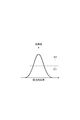
- FIG. 5 is a graph showing an example of the light intensity distribution of the laser light in the present embodiment.
- the horizontal axis indicates the radial position, and the vertical axis indicates the light intensity.
- a broken line E1 is a crystallization threshold value of the substrate 2
- a broken line E2 is a processing (melting) threshold value of the substrate 2.
- the laser light applied to the substrate 2 in this embodiment has a light intensity distribution such as a Gaussian distribution. That is, the light intensity at the center is the highest, and the light intensity gradually decreases as the distance from the center increases. The light intensity at the center exceeds the processing (melting) threshold of the substrate 2.
- the power density in the vicinity of the condensing points P1 and P2 increases, so that the substrate 2 is locally melted to form the perforations 12A and 12B. Further, around the perforations 12A and 12B, the power density becomes a size between the crystallization threshold value and the processing (melting) threshold value, and crystallized crystal regions 10A and 10B are formed.
- the heat treatment temperature is, for example, 760 ° C.
- the heat treatment time is, for example, 1 hour.
- the wavelength conversion optical device 1A according to this embodiment is manufactured through the above pre-process and the first processing process (including the laser light irradiation process).
- the wavelength conversion optical device 1A and the manufacturing method thereof according to the present embodiment when the surface (laser irradiation surface) of the substrate 2 is viewed, radial polarization ordered structures are alternately arranged on both sides of the virtual axis AX. Therefore, in the wavelength conversion region B1 including the virtual axis AX, polarization orientations that intersect the virtual axis AX and are opposite to each other (reversed by 180 degrees) appear periodically and alternately. Therefore, quasi phase matching by periodic polarization inversion can be performed on the light propagating through the wavelength conversion region B1.
- each of the crystal regions 10A and 10B of the wavelength conversion optical device 1A of the present embodiment can be easily formed by irradiating the substrate 2 with laser light having a wavelength included in the absorption wavelength band of the substrate 2.
- each of the crystal regions 10 ⁇ / b> A and 10 ⁇ / b> B is formed by irradiating the substrate 2 with laser light having a wavelength included in the absorption wavelength band of the substrate 2. That is, according to the wavelength conversion optical device 1A of this embodiment and the manufacturing method thereof, the polarization ordered structure for realizing the quasi phase matching can be formed by a simple method.
- the substrate 2 may include at least one of a Fresnoite crystal, BaO—TiO 2 —GeO 2 —SiO 2 glass, and SrO—TiO 2 —SiO 2 glass.
- the above-mentioned radial polarization ordered structure can be easily formed by laser light irradiation.
- the substrate 2 includes at least one of BaO—TiO 2 —GeO 2 —SiO 2 based glass and SrO—TiO 2 —SiO 2 based glass
- the substrate 2 is lanthanoid based, actinoid based, group 4 or You may include the metal contained in any group among 12 groups as an additive. Thereby, the absorption of the laser beam in the substrate 2 is enhanced, and the above-mentioned radial polarization ordered structure can be formed more efficiently.
- a CO 2 laser may be applied as a laser light source.
- the laser beam in the infrared region included in the absorption wavelength band of many substrates can be irradiated onto the substrate 2 in a state having a relatively large light intensity.
- FIG. 6 is a cross-sectional view illustrating a configuration of a wavelength conversion optical device 1B according to a first modification of the embodiment.
- the difference between this modification and the above embodiment is the shape of the crystal regions 10A and 10B. That is, the crystal regions 10A and 10B of the present modification are not circular but have a circular shape centered on the radial centers O1 and O2 of the radial polarization ordered structure. Radiation centers O1 and O2 are included in crystal regions 10A and 10B, respectively. Therefore, the wavelength conversion optical device 1B of this modification does not include the perforations 12A and 12B.
- FIG. 7 is a graph showing an example of the light intensity distribution of the laser beam for forming the crystal regions 10A and 10B of this modification.
- the horizontal axis indicates the radial position, and the vertical axis indicates the light intensity.
- a broken line E1 is a crystallization threshold value of the substrate 2
- a broken line E2 is a processing (melting) threshold value of the substrate 2.
- the laser light applied to the substrate 2 in the present modification has a top hat (flat top) light intensity distribution. That is, the light intensity is substantially constant in a region within a certain radius from the center, and the light intensity gradually decreases as the distance from the center increases.
- the light intensity in a region within a certain radius from the center is larger than the crystallization threshold value of the substrate 2 and smaller than the processing (melting) threshold value. According to such a light intensity distribution, since the power density in the vicinity of the condensing points P1 and P2 is smaller than the melting threshold, the substrate 2 is not melted and the perforations 12A and 12B are not formed. Further, in a region within a certain radius from the condensing points P1 and P2, the power density becomes a size between the crystallization threshold value and the processing (melting) threshold value, and the crystallized regions (crystal regions 10A and 10B) are present. It is formed.
- the same effects as those of the above-described embodiment can be obtained.
- the light intensity distribution of the laser light is made into a top hat shape, so that the melting of the substrate 2 in the center portion of each crystal region 10A, 10B is suppressed, and the center of each crystal region 10A, 10B is set.
- the occurrence of the perforations 12A and 12B can be suppressed. Thereby, deterioration of device performance due to cracks or the like caused by the perforations 12A and 12B can be suppressed.
- the laser light is applied to the substrate 2 through an optical component that converts the light intensity distribution of the laser light into a top hat shape as shown in FIG. What is necessary is just to be irradiated.
- an optical component include a diffractive optical element (DiffractiverOptical Element: DOE) or an aspheric lens.
- FIG. 8 is a diagram showing an example of an optical system for obtaining the light intensity distribution shown in FIG.
- an optical component OP1 is provided between a laser light source (which may include an optical system for collimating the laser light La) 30 that outputs collimated laser light La and a condensing point.
- a laser light source which may include an optical system for collimating the laser light La
- a condensing lens 40A and a diffractive optical element 50 are arranged in order from the laser light source 30 toward the condensing point.
- the light intensity distribution I1 of the laser light La between the laser light source 30 and the condenser lens 40A has the Gaussian distribution shape shown in FIG.
- the light intensity distribution I2 at the condensing point of the laser light La that has passed through the condensing lens 40A and the diffractive optical element 50 in this order has a top-hat shape as shown in FIG.
- the optical component OP1 may be replaced with the optical component OP2 including the aspheric lens 40B, and even when the optical component OP2 is disposed between the laser light source 30 and the condensing point of the laser light La,
- the shape of the light intensity distribution I2 at the condensing point is a top hat shape.
- FIG. 9A is a cross-sectional view showing a configuration of a wavelength conversion optical device 1C according to a second modification of the embodiment.
- the crystal regions 10A and 10B include the radial centers O1 and O2 of the radial polarization ordered structure, and the perforations 12A and 12B do not exist.
- the crystal regions 10A and 10B are alternately arranged in the direction D2 intersecting the optical waveguide direction D1.
- the wavelength conversion region B1 similar to that in the above embodiment can be formed by the crystal regions 10A and 10B located on both sides of a certain virtual axis AX.
- the wavelength conversion region B2 can be formed. That is, the wavelength conversion region B2 is a region that includes two virtual axes AX1 and AX2 and extends along the optical waveguide direction D1. The width along the direction D2 of the wavelength conversion region B2 is substantially equal to the period of the radiation center O1 along the direction D2 (that is, the period of the condensing point P1).
- FIG. 9B and FIG. 9C are graphs showing electric field distributions that can be effectively wavelength-converted in the wavelength conversion regions B1 and B2, respectively.
- the horizontal axis indicates the electric field strength, and the vertical axis indicates the position in the direction D2.
- the electric field intensity distribution becomes the LP 01 mode (base mode).
- the electric field intensity distribution becomes the LP 11 mode. Even in such an electric field mode, wavelength conversion is suitably performed.
- the electric field intensity distribution is LP 11 mode both before and after wavelength conversion.
- FIG. 10A is a plan view illustrating a configuration of a wavelength conversion optical device 1D according to a third modification of the embodiment.
- FIG. 10B is a cross-sectional view taken along the line IXb-IXb in FIG. 10A and shows a cross section that intersects the optical waveguide direction D1.
- FIG. 10C is a cross-sectional view taken along line IXc-IXc in FIG. 10A and shows a cross section intersecting with the optical waveguide direction D1.
- the substrate 2 has a channel optical waveguide structure 21 having the virtual axis AX as an optical axis.
- the channel optical waveguide structure 21 has a pair of side surfaces 21a and 21b extending along the virtual axis AX.
- one side surface 21a is located between the virtual axis AX and the radiation center O1.
- the other side surface 21b is located between the virtual axis AX and the radiation center O2.
- the side surfaces 21a and 21b are obtained, for example, by a second processing step that is performed before or after step S5 (step corresponding to a laser beam irradiation step) shown in FIG.
- the side surfaces 21a and 21b can be easily formed by removing the portion of the substrate 2 located outside the channel optical waveguide structure 21 by dry etching.
- the wavelength conversion optical device may include the substrate 2 having the channel optical waveguide structure 21 having the virtual axis AX as the optical axis. Moreover, the manufacturing method of the wavelength conversion optical device may further include a second processing step of forming the channel optical waveguide structure 21 on the substrate 2 as described above. Thereby, the light propagation efficiency on virtual axis line AX (wavelength conversion area
- a method (second processing step) for forming the channel optical waveguide structure on the substrate 2 For example, a method of cutting the substrate 2 with a dicing saw while leaving a portion to become a channel optical waveguide structure, a method of partially changing the refractive index by diffusing additives such as Ge and Ti into the substrate 2, or Examples thereof include a method of forming a channel optical waveguide structure inside the substrate 2 by a proton (H + ) exchange method.
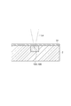
- FIG. 11 is a cross-sectional view showing a step in the manufacturing direction of the wavelength conversion optical device according to the fourth modification of the embodiment, and shows a cross section of the substrate 2 intersecting the optical waveguide direction D1.
- step S5 a step corresponding to a laser beam irradiation step
- the laser beam La is irradiated onto the substrate 2 on which the light absorbing material 31 is disposed.
- the light absorbing material 31 includes a material having absorption in a band including the wavelength of the laser light La.
- Examples of the method for arranging the light absorbing material 31 on the surface of the substrate 2 include coating, sputtering, and vapor deposition.
- the light absorbing material 31 is made of a material containing carbon, and in one example, is a carbon paste (a conductive paste in which carbon particles are added as a filler to a resin).
- the absorption of the laser beam La in the substrate 2 is enhanced, and the radial polarization ordered structure can be formed more efficiently.
- a carbon paste may be applied as the light absorbing material 31.
- the light absorbing material 31 that efficiently absorbs the laser beam power is easily disposed on the substrate 2.
- the carbon paste has a wide absorption band, light in a wavelength band oscillated by a fiber laser, a solid laser, or a semiconductor laser can be absorbed in addition to the CO 2 laser.
- the carbon paste can be easily removed by washing or the like after laser beam irradiation.
- FIG. 12 is a diagram illustrating a process in the manufacturing direction of the wavelength conversion optical device according to the fourth modification of the embodiment, and is a diagram for explaining a laser light irradiation process corresponding to process S5 in FIG. is there.
- the laser light La having a wavelength included in the absorption wavelength band of the substrate 2 is used.
- the laser light for forming the polarization ordered structure on the substrate surface or in the substrate.
- the first laser beam Lb1 for generating the excited electron high-density region and the second laser beam Lb2 for heating the excited electron high-density region are irradiated.
- the first laser light Lb1 is preferably an fs laser light having a wavelength that is out of the absorption wavelength band of the substrate 2 or a wavelength at which the amount of light absorption to the substrate 2 can be kept low, and a pulse width of less than 1 ps.
- the second laser light Lb2 has a wavelength outside the absorption wavelength band of the substrate 2 other than the condensing region of the first laser light Lb1, or a wavelength with which the light absorption amount to the substrate 2 can be kept low and a pulse width of 1 ps. As described above, a pulse laser beam of 1 ns or more is preferable.
- the second laser beam Lb2 is a CW laser beam having a wavelength that is out of the absorption wavelength band of the substrate 2 in a region other than the condensing region of the first laser beam Lb1, or a wavelength that can suppress the amount of light absorption to the substrate 2 low. Also good.
- a laser light source such as the above-described CO 2 laser, fiber laser, semiconductor laser, solid-state laser or the like is suitable.
- Non-patent Document 1 a laser beam having a pulse width of 1 ns or more (for example, a wavelength of 1070 nm) applicable to the second laser beam Lb2 is irradiated so as to overlap the excitation electron high-density region (the condensing region of the first laser beam Lb1).
- the light energy of the irradiated laser light is preferentially and selectively absorbed only in this region.
- Non-Patent Document 2 it is disclosed in Non-Patent Document 2 that the region that absorbs light energy (the excited electron high-density region is a region temporarily generated by irradiation with the first laser beam Lb1) effectively generates heat as a thermal filament.
- the amount of heat generated in the region (heat filament) that has absorbed the light energy of the second laser beam Lb2 depends on the irradiation time of the second laser beam Lb2. That is, when the calorific value increases, the temperature of the peripheral region centering on the hot filament also increases (region exceeding the crystallization threshold E1 shown in FIGS. 5 and 7). At this time, the peripheral region can be crystallized by controlling the amount of heat generated in the absorption region so that the temperature of the peripheral region is equal to or lower than the processing (melting) threshold E2.
- the substrate 2 having the channel optical waveguide structure 21 is prepared. From the first light source 30A, the surface of the substrate 2 or the condensing point P1 (corresponding to the radiation center O1) and the condensing point P2 (corresponding to the radiation center O2) shown in FIGS. Irradiated with a first laser beam Lb1 (fs laser beam) for generating an excited electron high density region inside.
- a first laser beam Lb1 fs laser beam
- a second laser beam Lb2 (pulse laser having a pulse width of 1 ps or more, preferably 1 ns or more, for heating the excited electron high-density region temporarily generated by the irradiation of the first laser beam Lb1.
- the substrate 2 is irradiated with light or CW laser light.
- the first laser beam Lb1 and the second laser beam Lb2 are irradiated coaxially.
- a common optical component OP3 condensing lens
- 40A condensing lens
- a half mirror 60 are arranged.
- Such a coaxial irradiation system has an advantage that it can be easily configured.
- the optical path of the first laser beam Lb1 and the optical path of the second laser beam Lb2 may be different.
- the first laser beam Lb1 and the second laser beam Lb2 are irradiated onto the substrate 2 in synchronization with each other.
- the first laser light Lb1 output from the first light source 30A is reflected by the half mirror 60 and travels toward the condensing lens 40A.
- the first laser light Lb1 that has passed through the condenser lens 40A is condensed near the surface of the substrate 2.
- a high density region of excited electrons is generated in the condensing region of the first laser beam Lb1.
- the second laser light Lb2 output from the second light source 30B passes through the half mirror 60 and travels toward the condenser lens 40A.
- the second laser light Lb2 that has passed through the condensing lens 40A is condensed so as to overlap the high density region of excited electrons.
- the light energy of the second laser beam Lb2 is efficiently absorbed in the excited electron high-density region.
- the excited electron high-density region functions as the hot filament 110.
- crystal regions 10A and 10B are formed in the substrate 2 that are oriented perpendicular to the contour lines of the temperature in the peripheral region of the hot filament 110.
- FIG. 13A is a schematic diagram for explaining the polarization direction in the crystal region formed using the laser beam having the light intensity distribution shown in FIG.
- FIG. 13B is a schematic diagram for explaining a polarization direction in a crystal region formed by the method of manufacturing a wavelength conversion optical device according to the fifth modification.
- the orientation in the depth direction of the irradiation material (substrate 2) is set on the surface of the substrate 2 as shown in FIG. 13A. However, it is not completely parallel, and is slightly inclined in the depth direction.
- the depth of the irradiation material (substrate 2) is increased by the hot filament effect.
- the temperature is selectively raised along the vertical direction. Therefore, as shown in FIG. 13B, the orientation of the irradiation material in the depth direction is parallel to the surface of the substrate 2 in the region ⁇ .
- the shape of the perforations (laser processing traces) 12A and 12B depends on the fs laser condensing condition, but depending on the irradiation conditions, processing of a high aspect ratio shape having a diameter of about 10 ⁇ m and a depth of 100 ⁇ m or more is possible. (See Non-Patent Document 2 above).
- the shape of the hot filament 110 depending on the processing shape is formed perpendicular to the depth direction, and is polarized perpendicular to the contour line of the temperature, so that the polarization in the region ⁇ shown in FIG. However, it will be oriented in parallel indefinitely. As a result, highly efficient wavelength conversion is possible depending on the polarization of incident light.
- a Ti: S laser, a 1 ⁇ m band fiber laser, or SHG of these light sources is effective.
- FIG. 14A, FIG. 15A, and FIG. 16A are optical microscope images showing states after irradiating laser light from a CO 2 laser onto SrO—TiO 2 —SiO 2 glass, respectively.
- FIG. 14A shows a state where the output of the laser beam is 7.8 W and the irradiation time is 2 seconds.
- FIG. 15A shows a state where the output of the laser beam is 7.8 W and the irradiation time is 1 second.
- FIG. 16A shows a state where the laser beam output is 3.28 W and the irradiation time is 2 seconds.
- 14B, 15B, and 16B are partially enlarged views of FIGS. 14A, 15A, and 16A, respectively. Under any irradiation condition, a perforation (laser processing mark) 12 was generated, while a crystallized region, that is, a crystal region 10 (corresponding to the crystal regions 10A and 10B) was generated around the perforation.
- FIG. 17 is an image showing the measurement result of second harmonic generation (SHG).
- FIG. 17 also shows the polarization direction of the laser light used for the measurement.
- the SrO—TiO 2 —SiO 2 glass has a second-order nonlinear optical constant (d constant) of d 31 > d 33 , and in this measurement, d 31 SH light is preferentially observed.
- d constant nonlinear optical constant
- a pair of SH light was observed in the crystal region 10 formed in an annular shape. These SH lights were generated on a straight line that passed through the center of the crystal region 10 and extended in a direction orthogonal to the polarization direction.
- This SH light is SH light due to the d 31 component, and the direction of polarization of this SH light is perpendicular to the incident wavefront. That is, the direction of polarization is along a straight line connecting the generation region of SH light and the center of the crystal region 10 and is understood to be radial. From this, it was shown that the crystal region 10 having a radial polarization ordered structure can be formed by irradiating the substrate 2 with laser light.
- the wavelength conversion optical device of the present disclosure is not limited to the above-described embodiment (including modifications), and various other modifications are possible. For example, you may combine the above-mentioned embodiment and each modification according to the required purpose and effect.
- the Fresnoite-type crystal, BaO—TiO 2 —GeO 2 —SiO 2 glass, and SrO—TiO 2 —SiO 2 glass are exemplified as the substrate material.
- various materials can be applied that are crystalline or amorphous and transparent to the desired wavelength.
- 1A, 1B, 1C, 1D ... wavelength conversion optical device 2 ... substrate, 2a, 2b ... end face, 2c, 2d ... region, 10, 10A, 10B ... crystal region, 12A, 12B ... perforation (laser processing trace), 21 ... Channel optical waveguide structure, 21a, 21b ... Side face, 30 ... Laser light source, 30A ... First light source, 30B ... Second light source, 31 ... Light absorber, 40A ... Condensing lens, 40B ... Aspheric lens, 50 ... Diffraction Optical element 60 ... half mirror, A1, A2 ... spontaneous polarization, AX, AX1, AX2 ... virtual axis, B1, B2 ...
- wavelength conversion region B1a ... one end, B1b ... other end, D1 ... optical waveguide direction, D2 ... direction , La ... laser light, Lb1 ... first laser light, Lb2 ... second laser light, O1, O2 ... radiation center, P1, P2 ... condensing point, OP1, OP2, OP3 ... optical components.
Landscapes
- Physics & Mathematics (AREA)
- Nonlinear Science (AREA)
- General Physics & Mathematics (AREA)
- Optics & Photonics (AREA)
- Chemical & Material Sciences (AREA)
- Crystallography & Structural Chemistry (AREA)
- Optical Modulation, Optical Deflection, Nonlinear Optics, Optical Demodulation, Optical Logic Elements (AREA)
Abstract
An optical wavelength converter according to an embodiment comprises: a substrate made of a crystalline material or an amorphous material; a plurality of first crystalline regions having a first radially-polarized ordered structure; and a plurality of second crystalline regions having a second radially-polarized ordered structure. The substrate has defined thereon a first region and a second region directly adjacent to each other with a virtual axial line therebetween when viewed from a reference direction perpendicular to the virtual axial line. The radial centers of the first radially-polarized ordered structure located in the first region and the radial centers of the second radially-polarized ordered structure located in the second region are arranged alternately along the virtual axial line. A part of the plurality of first crystalline regions protrudes into the second region. A part of the plurality of second crystalline regions protrudes into the first region.
Description
本開示は、波長変換光デバイスおよび波長変換光デバイスの製造方法に関するものである。
The present disclosure relates to a wavelength conversion optical device and a method for manufacturing the wavelength conversion optical device.
本願は、2018年2月8日に出願された日本特許出願第2018-021281号による優先権を主張するものであり、その内容に依拠すると共に、その全体を参照して本明細書に組み込む。
This application claims priority from Japanese Patent Application No. 2018-021281 filed on Feb. 8, 2018, and depends on the contents thereof, and is incorporated herein by reference in its entirety.
2次非線形光学現象を利用する光デバイスに用いられる材料としては、LiNbO3(LN)結晶、KTiOPO4(KTP)結晶、LiB3O5(LBO)結晶、あるいはβ-BaB2O4(BBO)結晶のような強誘電体光学結晶が主流である。これらの結晶を利用した光デバイスは、波長変換を基軸とした広範な応用分野に展開されている。例えば、レーザ加工分野では、これらの結晶を利用した光デバイスは、光ファイバレーザの第二高調波発生(SHG:Second Harmonic Generation)による短波長化に用いられている。ビームスポット径を小さくできることから、このような光デバイスは微細な加工を可能にする。光通信分野では、波長分割多重(Wavelength Division Multiplexing:WDM)光通信における波長資源の有効活用のため、これらの結晶を利用した光デバイスは、CバンドのWDM信号からLバンドへの一括多重変換(simultaneous wavelength conversion)を行う波長変換光デバイスとして用いられている。更に、計測分野では、水素結合などに起因する分子間振動が観測できるテラヘルツ分光が着目されており、これらの結晶を利用した光デバイスは、そのテラヘルツ光を発生させる光源に使用されている。
Materials used for optical devices utilizing second-order nonlinear optical phenomena include LiNbO 3 (LN) crystal, KTiOPO 4 (KTP) crystal, LiB 3 O 5 (LBO) crystal, or β-BaB 2 O 4 (BBO). Ferroelectric optical crystals such as crystals are the mainstream. Optical devices using these crystals have been developed in a wide range of application fields based on wavelength conversion. For example, in the laser processing field, optical devices using these crystals are used for shortening the wavelength by second harmonic generation (SHG) of an optical fiber laser. Since the beam spot diameter can be reduced, such an optical device enables fine processing. In the optical communication field, in order to effectively use wavelength resources in wavelength division multiplexing (WDM) optical communication, optical devices using these crystals are capable of batch multiplexing conversion from a C-band WDM signal to an L-band ( It is used as a wavelength conversion optical device that performs simultaneous wavelength conversion. Further, in the measurement field, terahertz spectroscopy capable of observing intermolecular vibrations caused by hydrogen bonds or the like has attracted attention, and optical devices using these crystals are used as light sources for generating the terahertz light.
最近では、化合物半導体結晶であるGaAs、GaP、GaN、CdTe、ZnSe、ZnO等も、2次非線形光学現象を利用する光デバイスの材料として用いられている。これらの材料は、大きな2次の非線形光学定数を有することに加え、2次非線形光デバイスに不可欠な周期的空間反転構造(periodically-poled structure)の作製技術の著しい進歩により、2次非線形デバイスの材料として注目されている。
Recently, compound semiconductor crystals such as GaAs, GaP, GaN, CdTe, ZnSe, ZnO, and the like have also been used as materials for optical devices utilizing the second-order nonlinear optical phenomenon. In addition to having a large second-order nonlinear optical constant, these materials have a remarkable progress in the fabrication technology of periodic-poled structures essential for second-order nonlinear optical devices. It is attracting attention as a material.
波長変換の方式は、角度位相整合(angle phase matching)と、周期分極反転(periodically-poling)による擬似位相整合(QPM:Quasi Phase Matching)とに分類できる。これらのうち、擬似位相整合は、周期分極反転幅(poling pitch)を適切に設計することにより、様々な位相整合波長の生成を可能とし、材料の透明領域の全てにおいて波長変換を可能とする。また、擬似位相整合は、角度位相整合によるウォークオフ角が無いことから、ビーム品質が良好な上に、相互作用長の長尺化が可能であり、高効率化や結合損の抑制に適していることから、加工および計測等において有効な方式である。
The wavelength conversion method can be classified into angle phase matching (angle phase matching) and quasi phase matching (QPM: Quasi Phase matching) by periodic polarization inversion. Among these, the quasi-phase matching enables generation of various phase matching wavelengths by appropriately designing the periodical polarization inversion width (poling pitch), and enables wavelength conversion in all the transparent regions of the material. Pseudo phase matching does not have a walk-off angle due to angular phase matching, so that the beam quality is good and the interaction length can be increased, making it suitable for increasing efficiency and suppressing coupling loss. Therefore, it is an effective method in processing and measurement.
本開示の波長変換光デバイスは、結晶質または非晶質からなる基板と、放射状の第1分極秩序構造をそれぞれ有する複数の第1結晶領域と、放射状の第2分極秩序構造をそれぞれ有する複数の第2結晶領域と、を備える。基板は、当該基板内に設定される或る仮想軸線に直交する基準方向から該基板を見たときに仮想軸線を挟んで直接隣接する第1領域と第2領域が規定される。第1分極秩序構造の放射中心は、基板の第1領域において仮想軸線に沿って配置されている。複数の第1結晶領域は、基準方向から基板を見たときに、それぞれの一部が仮想軸線を跨いで第2領域にはみ出している。第2分極秩序構造の放射中心は、基板の第2領域において仮想軸線に沿って配置されるとともに第2分極秩序構造の放射中心が仮想軸線に沿って第1分極秩序構造の放射中心と交互に配置されている。複数の第2結晶領域は、基準方向から基板を見たときに、それぞれの一部が仮想軸線を跨いで第1領域にはみ出している。
The wavelength conversion optical device of the present disclosure includes a crystalline or amorphous substrate, a plurality of first crystal regions each having a radial first polarization order structure, and a plurality of each having a radial second polarization order structure. A second crystal region. When the substrate is viewed from a reference direction orthogonal to a certain virtual axis set in the substrate, a first region and a second region that are directly adjacent to each other with the virtual axis interposed therebetween are defined. The radiation center of the first polarization ordered structure is arranged along the virtual axis in the first region of the substrate. When the substrate is viewed from the reference direction, each of the plurality of first crystal regions protrudes into the second region across the virtual axis. The radiation center of the second polarization ordered structure is disposed along the virtual axis in the second region of the substrate, and the radiation center of the second polarization ordered structure alternates with the radiation center of the first polarization ordered structure along the virtual axis. Has been placed. When the substrate is viewed from the reference direction, each of the plurality of second crystal regions protrudes into the first region across the virtual axis.
本開示の波長変換光デバイスの製造方法は、基板を用意する前工程と、放射状の第1分極秩序構造をそれぞれ有する複数の第1結晶領域と放射状の第2分極秩序構造をそれぞれ有する複数の第2結晶領域と、を基板に設ける第1加工工程と、を備える。基板は、結晶質または非晶質からなる。また、基板は、当該基板内に設定される或る仮想軸線に直交する基準方向から該基板を見たときに仮想軸線を挟んで直接隣接する第1領域と第2領域が規定される。複数の第1結晶領域の第1分極秩序構造における放射中心は、基板の第1領域において仮想軸線に沿って配置されている。また、複数の第1結晶領域は、基準方向から基板を見たときに、それぞれの一部が仮想軸線を跨いで第2領域にはみ出している。一方、複数の第2結晶領域の第2分極秩序構造における放射中心は、基板の第2領域において仮想軸線に沿って配置されている。また、複数の第2結晶領域は、基準方向から基板を見たときに、第2分極秩序構造の放射中心が仮想軸線に沿って第1分極秩序構造の前記放射中心と交互に配置された状態でそれぞれの一部が仮想軸線を跨いで第1領域にはみ出している。第1加工工程はレーザ光照射工程を含み、レーザ光照射工程は、複数の第1結晶領域の第1分極秩序構造における放射中心に対応した複数の第1集光点それぞれと複数の第2結晶領域の第2分極秩序構造における放射中心に対応した複数の第2集光点のそれぞれに対して、第1および第2分極秩序構造を形成するためのレーザ光を照射する。
The method for manufacturing a wavelength conversion optical device according to the present disclosure includes a pre-process for preparing a substrate, a plurality of first crystal regions each having a radial first polarization order structure, and a plurality of first crystal structures each having a radial second polarization order structure. A first processing step of providing a two-crystal region on the substrate. The substrate is made of crystalline or amorphous. Further, when the substrate is viewed from a reference direction orthogonal to a certain virtual axis set in the substrate, a first region and a second region that are directly adjacent to each other with the virtual axis interposed therebetween are defined. Radiation centers in the first polarization ordered structure of the plurality of first crystal regions are arranged along the virtual axis in the first region of the substrate. In addition, when the substrate is viewed from the reference direction, each of the plurality of first crystal regions protrudes into the second region across the virtual axis. On the other hand, the radiation center in the second polarization ordered structure of the plurality of second crystal regions is arranged along the virtual axis in the second region of the substrate. The plurality of second crystal regions are arranged such that when the substrate is viewed from the reference direction, the radiation centers of the second polarization ordered structure are alternately arranged with the radiation centers of the first polarization ordered structure along the virtual axis. Thus, each part protrudes into the first region across the virtual axis. The first processing step includes a laser beam irradiation step, and the laser beam irradiation step includes a plurality of first condensing points and a plurality of second crystals corresponding to the radiation centers in the first polarization ordered structure of the plurality of first crystal regions. Laser light for forming the first and second polarization ordered structures is irradiated to each of the plurality of second condensing points corresponding to the emission centers in the second polarization ordered structure of the region.
[本開示が解決しようとする課題]
発明者らは、従来の波長変換光デバイスについて検討した結果、以下のような課題を発見した。すなわち、擬似位相整合を行う波長変換光デバイスとして、ガラスの自在成形加工と波長変換技術の組み合わせにより得られる光デバイスが提案されている(例えば特許文献1を参照)。このような波長変換光デバイスの利点は、基板材料がガラスであることからファイバ形や薄膜形など様々な形状に加工することができ、その形状に波長変換機能を付与できる点である。特許文献1には、電界を印加した状態でレーザを照射することにより、分極方向(polarization orientation)で規定される分極秩序構造(polarization-ordered structure)を形成する方法が記載されている。一方、擬似位相整合を実現するための分極秩序構造は微細であり、また、互いに隣り合う分極秩序構造同士の間隔も極めて短い。このような構造では電界を印加するための正電極と負電極との間隔が狭くなるので、高い電圧を印加したときの絶縁破壊を避けるために加工工程が複雑化するという課題がある。 [Problems to be solved by the present disclosure]
As a result of examining the conventional wavelength conversion optical device, the inventors have found the following problems. That is, as a wavelength conversion optical device that performs quasi phase matching, an optical device obtained by a combination of glass free-form processing and wavelength conversion technology has been proposed (see, for example, Patent Document 1). The advantage of such a wavelength conversion optical device is that since the substrate material is glass, it can be processed into various shapes such as a fiber shape and a thin film shape, and a wavelength conversion function can be imparted to the shape.Patent Document 1 describes a method of forming a polarization-ordered structure defined by a polarization orientation by irradiating a laser with an electric field applied. On the other hand, the polarization order structure for realizing quasi phase matching is fine, and the interval between the polarization order structures adjacent to each other is extremely short. In such a structure, since the interval between the positive electrode and the negative electrode for applying an electric field is narrowed, there is a problem that the machining process is complicated in order to avoid dielectric breakdown when a high voltage is applied.
発明者らは、従来の波長変換光デバイスについて検討した結果、以下のような課題を発見した。すなわち、擬似位相整合を行う波長変換光デバイスとして、ガラスの自在成形加工と波長変換技術の組み合わせにより得られる光デバイスが提案されている(例えば特許文献1を参照)。このような波長変換光デバイスの利点は、基板材料がガラスであることからファイバ形や薄膜形など様々な形状に加工することができ、その形状に波長変換機能を付与できる点である。特許文献1には、電界を印加した状態でレーザを照射することにより、分極方向(polarization orientation)で規定される分極秩序構造(polarization-ordered structure)を形成する方法が記載されている。一方、擬似位相整合を実現するための分極秩序構造は微細であり、また、互いに隣り合う分極秩序構造同士の間隔も極めて短い。このような構造では電界を印加するための正電極と負電極との間隔が狭くなるので、高い電圧を印加したときの絶縁破壊を避けるために加工工程が複雑化するという課題がある。 [Problems to be solved by the present disclosure]
As a result of examining the conventional wavelength conversion optical device, the inventors have found the following problems. That is, as a wavelength conversion optical device that performs quasi phase matching, an optical device obtained by a combination of glass free-form processing and wavelength conversion technology has been proposed (see, for example, Patent Document 1). The advantage of such a wavelength conversion optical device is that since the substrate material is glass, it can be processed into various shapes such as a fiber shape and a thin film shape, and a wavelength conversion function can be imparted to the shape.
本開示は、このような課題を解決するためになされたものであり、擬似位相整合を実現するための分極秩序構造を簡易な方法により形成することができる波長変換光デバイス、および該波長変換光デバイスの製造方法を提供することを目的とする。
The present disclosure has been made to solve such a problem, and a wavelength conversion optical device capable of forming a polarization ordered structure for realizing quasi phase matching by a simple method, and the wavelength conversion light An object of the present invention is to provide a device manufacturing method.
[本開示の効果]
本開示の波長変換光デバイスおよび波長変換光デバイスの製造方法によれば、仮想軸線を挟む一対の領域において、該仮想軸線に沿って交互に放射状の分極秩序構造を有する結晶領域が形成される。 [Effects of the present disclosure]
According to the wavelength conversion optical device and the method of manufacturing a wavelength conversion optical device of the present disclosure, in a pair of regions sandwiching the virtual axis, crystal regions having a radial polarization ordered structure are alternately formed along the virtual axis.
[本開示の実施形態の説明]
最初に本開示の実施形態の内容をそれぞれ個別に列挙して説明する。 [Description of Embodiment of the Present Disclosure]
First, the contents of the embodiments of the present disclosure will be listed and described individually.
最初に本開示の実施形態の内容をそれぞれ個別に列挙して説明する。 [Description of Embodiment of the Present Disclosure]
First, the contents of the embodiments of the present disclosure will be listed and described individually.
(1)本開示の一実施形態に係る波長変換光デバイスは、その一態様として、結晶質または非晶質からなる基板と、放射状の第1分極秩序構造をそれぞれ有する複数の第1結晶領域と、放射状の第2分極秩序構造をそれぞれ有する複数の第2結晶領域と、を備える。基板は、当該基板内に設定される或る仮想軸線に直交する基準方向から該基板を見たときに仮想軸線を挟んで直接隣接する第1領域と第2領域が規定される。第1分極秩序構造の放射中心は、基板の第1領域において仮想軸線に沿って配置されている。複数の第1結晶領域は、基準方向から基板を見たときに、それぞれの一部が仮想軸線を跨いで第2領域にはみ出している。第2分極秩序構造の放射中心は、基板の第2領域において仮想軸線に沿って配置されるとともに第2分極秩序構造の放射中心が仮想軸線に沿って第1分極秩序構造の放射中心と交互に配置されている。複数の第2結晶領域は、基準方向から基板を見たときに、それぞれの一部が仮想軸線を跨いで第1領域にはみ出している。
(1) A wavelength conversion optical device according to an embodiment of the present disclosure includes, as an aspect thereof, a substrate made of a crystalline material or an amorphous material, and a plurality of first crystal regions each having a radial first polarization ordered structure. And a plurality of second crystal regions each having a radial second polarization ordered structure. When the substrate is viewed from a reference direction orthogonal to a certain virtual axis set in the substrate, a first region and a second region that are directly adjacent to each other with the virtual axis interposed therebetween are defined. The radiation center of the first polarization ordered structure is arranged along the virtual axis in the first region of the substrate. When the substrate is viewed from the reference direction, each of the plurality of first crystal regions protrudes into the second region across the virtual axis. The radiation center of the second polarization ordered structure is disposed along the virtual axis in the second region of the substrate, and the radiation center of the second polarization ordered structure alternates with the radiation center of the first polarization ordered structure along the virtual axis. Has been placed. When the substrate is viewed from the reference direction, each of the plurality of second crystal regions protrudes into the first region across the virtual axis.
上述のような構造を有する波長変換デバイスでは、仮想軸線の両側に放射状の分極秩序構造が交互に並んでいる。したがって、仮想軸線上においては、仮想軸線と交差し且つ互いに逆向きである分極配向が交互に現れる。故に、仮想軸線上を伝搬する光に対し、周期分極反転による擬似位相整合を行うことができる。また、当該波長変換光デバイスの各結晶領域は、基板の吸収波長に含まれる波長のレーザ光を基板に照射すること、または、基板表面または内部に熱源を形成することにより、容易に形成可能である。
In the wavelength conversion device having the structure as described above, radial polarization ordered structures are alternately arranged on both sides of the virtual axis. Therefore, on the virtual axis, polarization orientations that intersect the virtual axis and are opposite to each other appear alternately. Therefore, quasi-phase matching by periodic polarization inversion can be performed on the light propagating on the virtual axis. In addition, each crystal region of the wavelength conversion optical device can be easily formed by irradiating the substrate with laser light having a wavelength included in the absorption wavelength of the substrate, or by forming a heat source on or inside the substrate. is there.
(2)本実施形態の一態様として、基板は、仮想軸線を光軸とするチャネル光導波路構造を有するのが好ましい。このようなチャネル光導波路構造は、仮想軸線上における光伝搬効率を高めることができる。本実施形態の一態様として、基板は、フレスノイト型結晶、BaO-TiO2-GeO2-SiO2系ガラス、およびSrO-TiO2-SiO2系ガラスのうち少なくとも一つを含むのが好ましい。例えばこれらの基板において、上述の放射状の分極秩序構造がレーザ光の照射によって容易に形成され得る。更に、本実施形態の一態様として、基板は、BaO-TiO2-GeO2-SiO2系ガラスおよびSrO-TiO2-SiO2系ガラスのうち少なくとも一つを含み、更に添加物として、ランタノイド系、アクチノイド系、4族ないし12族のうち何れかの群に含まれる金属を含んでもよい。この場合、基板におけるレーザ光の吸収が高められ、上述の放射状の分極秩序構造が更に効率良く形成され得る。
(2) As one aspect of the present embodiment, the substrate preferably has a channel optical waveguide structure having a virtual axis as an optical axis. Such a channel optical waveguide structure can increase the light propagation efficiency on the virtual axis. As one aspect of the present embodiment, the substrate preferably includes at least one of a Fresnoite crystal, BaO—TiO 2 —GeO 2 —SiO 2 glass, and SrO—TiO 2 —SiO 2 glass. For example, in these substrates, the above-mentioned radial polarization ordered structure can be easily formed by laser light irradiation. Furthermore, as one aspect of the present embodiment, the substrate includes at least one of BaO—TiO 2 —GeO 2 —SiO 2 glass and SrO—TiO 2 —SiO 2 glass, and further includes a lanthanoid-based additive as an additive. , Actinoids, and metals included in any group of groups 4 to 12. In this case, the absorption of the laser beam in the substrate is enhanced, and the above-mentioned radial polarization ordered structure can be formed more efficiently.
(3) 本開示の一実施形態に係る波長変換光デバイスの製造方向は、その一態様として、基板を用意する前工程と、放射状の第1分極秩序構造をそれぞれ有する複数の第1結晶領域と放射状の第2分極秩序構造をそれぞれ有する複数の第2結晶領域と、を基板に設ける第1加工工程と、を備える。基板は、結晶質または非晶質からなる。また、基板は、当該基板内に設定される或る仮想軸線に直交する基準方向から該基板を見たときに仮想軸線を挟んで直接隣接する第1領域と第2領域が規定される。複数の第1結晶領域の第1分極秩序構造における放射中心は、基板の第1領域において仮想軸線に沿って配置されている。また、複数の第1結晶領域は、基準方向から基板を見たときに、それぞれの一部が仮想軸線を跨いで第2領域にはみ出している。一方、複数の第2結晶領域の第2分極秩序構造における放射中心は、基板の第2領域において仮想軸線に沿って配置されている。また、複数の第2結晶領域は、基準方向から基板を見たときに、第2分極秩序構造の放射中心が仮想軸線に沿って第1分極秩序構造の前記放射中心と交互に配置された状態でそれぞれの一部が仮想軸線を跨いで第1領域にはみ出している。
(3) The manufacturing direction of the wavelength conversion optical device according to an embodiment of the present disclosure includes, as one aspect, a pre-process for preparing a substrate, and a plurality of first crystal regions each having a radial first polarization ordered structure, A first processing step of providing a plurality of second crystal regions each having a radial second polarization ordered structure on a substrate. The substrate is made of crystalline or amorphous. Further, when the substrate is viewed from a reference direction orthogonal to a certain virtual axis set in the substrate, a first region and a second region that are directly adjacent to each other with the virtual axis interposed therebetween are defined. Radiation centers in the first polarization ordered structure of the plurality of first crystal regions are arranged along the virtual axis in the first region of the substrate. In addition, when the substrate is viewed from the reference direction, each of the plurality of first crystal regions protrudes into the second region across the virtual axis. On the other hand, the radiation center in the second polarization ordered structure of the plurality of second crystal regions is arranged along the virtual axis in the second region of the substrate. The plurality of second crystal regions are arranged such that when the substrate is viewed from the reference direction, the radiation centers of the second polarization ordered structure are alternately arranged with the radiation centers of the first polarization ordered structure along the virtual axis. Thus, each part protrudes into the first region across the virtual axis.
特に、第1加工工程はレーザ光照射工程を含む。レーザ光照射工程は、複数の第1結晶領域の第1分極秩序構造における放射中心に対応した複数の第1集光点それぞれと複数の第2結晶領域の第2分極秩序構造における放射中心に対応した複数の第2集光点のそれぞれに対して、第1および第2分極秩序構造を形成するためのレーザ光を照射する。当該波長変換光デバイスの各結晶領域は、基板の吸収波長に含まれる波長のレーザ光を基板に照射すること、または、基板表面または内部に熱源を形成することにより、容易に形成可能である。すなわち、当該製造方法によれば、擬似位相整合を実現するための分極秩序構造を簡易な方法により形成することを可能にする。
In particular, the first processing step includes a laser beam irradiation step. The laser beam irradiation step corresponds to each of the plurality of first condensing points corresponding to the radiation center in the first polarization order structure of the plurality of first crystal regions and to the radiation center in the second polarization order structure of the plurality of second crystal regions. Each of the plurality of second condensing points is irradiated with laser light for forming the first and second polarization ordered structures. Each crystal region of the wavelength conversion optical device can be easily formed by irradiating the substrate with laser light having a wavelength included in the absorption wavelength of the substrate, or by forming a heat source on or inside the substrate. That is, according to the manufacturing method, it is possible to form a polarization ordered structure for realizing quasi phase matching by a simple method.
(4)本実施形態の一態様として、分極秩序構造を形成するためのレーザ光は、基板の吸収波長帯域に含まれる波長を有するのが好ましい。この場合、レーザ光照射により基板を直接加熱することが可能になる。また、本実施形態の一態様として、分極秩序構造を形成するためのレーザ光は、基板表面または基板内に励起電子高密度領域を発生させるための第1レーザ光と、該励起電子高密度領域を加熱するための第2レーザ光を含んでもよい。このような構成において、レーザ光照射工程は、第2レーザ光の集光領域が第1レーザ光の集光領域とオーバーラップした状態で複数の第1集光点のそれぞれおよび複数の第2集光点のそれぞれに対して、第1レーザ光および第2レーザ光を照射する。この場合、分極秩序構造を形成するための熱源を基板表面または内部の任意の位置に形成することが可能になる。
(4) As one aspect of the present embodiment, the laser light for forming the polarization ordered structure preferably has a wavelength included in the absorption wavelength band of the substrate. In this case, the substrate can be directly heated by laser light irradiation. Further, as one aspect of the present embodiment, the laser light for forming the polarization ordered structure includes the first laser light for generating the excited electron high-density region on the substrate surface or in the substrate, and the excited electron high-density region. The second laser beam for heating may be included. In such a configuration, the laser beam irradiation step includes a plurality of first focusing points and a plurality of second focusing points in a state where the focusing region of the second laser beam overlaps the focusing region of the first laser beam. The first laser beam and the second laser beam are irradiated to each of the light spots. In this case, a heat source for forming the polarization ordered structure can be formed at any position on the substrate surface or inside.
(5)なお、上記第1レーザ光および第2レーザ光には、種々のレーザ光が適用可能である。例えば、本実施形態の一態様として、第1レーザ光は、基板の吸収波長帯域から外れた波長または該基板への光吸収量が低く抑えられる波長を有するとともにパルス幅1ps未満のfs(femtosecond)レーザ光を含むのが好ましい。また、本実施形態の一態様として、第2レーザ光は、第1レーザ光の集光領域以外における基板の吸収波長帯域から外れた波長または該基板への光吸収量が低く抑えられる波長を有するとともにパルス幅1ps以上、好ましくは1ns以上のパルスレーザ光を含むのが好ましい。本実施形態の一態様として、第2レーザ光は、第1レーザ光の集光領域以外における基板の吸収波長帯域から外れた波長または該基板への光吸収量が低く抑えられる波長を有するCW(Continuous Wave)レーザ光を含んでもよい。
(5) Various laser beams can be applied to the first laser beam and the second laser beam. For example, as one aspect of the present embodiment, the first laser beam has a wavelength that is out of the absorption wavelength band of the substrate or a wavelength at which the amount of light absorption to the substrate can be kept low, and fs (femtosecond) with a pulse width of less than 1 ps. It is preferable to include a laser beam. Further, as one aspect of the present embodiment, the second laser light has a wavelength that is out of the absorption wavelength band of the substrate in a region other than the condensing region of the first laser light or a wavelength that can suppress light absorption to the substrate low. A pulse laser beam having a pulse width of 1 ps or more, preferably 1 ns or more is preferably included. As one aspect of the present embodiment, the second laser light has a wavelength outside the absorption wavelength band of the substrate in a region other than the light condensing region of the first laser light, or a wavelength that can suppress the amount of light absorption to the substrate low. Continuous (Wave) Laser light may be included.
第1レーザ光の集光領域は、該第1レーザ光の集光点を中心とした励起された電子が高密度に発生する領域(励起電子高密度領域)を意味し、励起された電子の数密度が1019/cm3以上の領域として規定される。また、第1レーザ光の集光領域と第2レーザ光の集光領域とがオーバーラップした状態(以下、オーバーラップ状態という)は、第1レーザ光の集光点と第2レーザ光の集光点とが一致している状態の他、集光点が一致していない状態も含む。具体的には、第2レーザ光の集光点が励起電子高密度領域(第1レーザ光の集光領域)内に存在していない場合であっても、このオーバーラップ状態には、励起電子高密度領域全体または少なくともその一部が第2レーザ光の照射領域内に存在するよう、該第2レーザ光のスポット径が絞り込まれた状態が含まれる。第1レーザ光(fsレーザ光)が非晶質の基板、例えば前駆体ガラスの内部に集光されると、該fsレーザ光が集光された領域には、一時的に励起電子高密度領域が発生する。この励起電子高密度領域(第1レーザ光の集光領域)が発生している間に該励起電子高密度領域にその集光領域がオーバーラップするように第2レーザ光(パルスレーザ光またはCWレーザ光)が照射されると、該励起電子高密度領域の局所領域のみにおいて優先的かつ選択的に光吸収を誘発させられることが可能になる。このとき、光吸収領域(第1および第2レーザ光のオーバーラップされた集光領域)では熱が発生し、結晶領域が形成される。基板の表面または内部において、第1および第2レーザ光のオーバーラップされた集光領域を三次元的に走査することで、バルク形状やファイバ形状等、様々な形態の高効率な波長変換光デバイスが実現され得る。
The condensing region of the first laser light means a region where excited electrons centered on the condensing point of the first laser light are generated at a high density (excited electron high density region). The number density is defined as a region of 10 19 / cm 3 or more. In addition, a state where the light condensing region of the first laser light and the light condensing region of the second laser light overlap (hereinafter referred to as an overlap state) is a point where the light condensing point of the first laser light and the second laser light are collected. In addition to the state where the light spot is coincident, the state where the condensing point is not coincident is also included. Specifically, even when the condensing point of the second laser beam does not exist in the high density region of the excited electrons (the condensing region of the first laser beam), the overlapped state is in the excited state. This includes a state in which the spot diameter of the second laser light is narrowed down so that the entire high-density region or at least a part thereof exists in the irradiation region of the second laser light. When the first laser light (fs laser light) is condensed inside an amorphous substrate, for example, precursor glass, the region where the fs laser light is condensed temporarily has a high density of excited electrons. Will occur. While this excitation electron high density region (condensation region of the first laser light) is generated, the second laser light (pulse laser light or CW) is used so that the excitation electron high density region overlaps with the excitation electron high density region. When the laser beam is irradiated, light absorption can be preferentially and selectively induced only in the local region of the high density region of excited electrons. At this time, heat is generated in the light absorption region (the condensing region where the first and second laser beams overlap), and a crystal region is formed. High-efficiency wavelength conversion optical devices in various forms such as bulk shape and fiber shape by three-dimensionally scanning the overlapped condensing region of the first and second laser beams on the surface or inside of the substrate Can be realized.
(6)本実施形態の一態様として、当該製造方法は、レーザ光照射工程の前または後に、仮想軸線を光軸とするチャネル光導波路構造を基板に形成する第2加工工程を更に備えてもよい。これにより、仮想軸線上における光伝搬効率を高めることができる。また、本実施形態の一態様として、チャネル光導波路構造は、ダイシングソーまたはドライエッチングにより形成されるのが好ましい。これにより、結晶質または非晶質からなる基板にチャネル光導波路構造を容易に形成することが可能になる。
(6) As an aspect of the present embodiment, the manufacturing method may further include a second processing step of forming a channel optical waveguide structure with the virtual axis as the optical axis on the substrate before or after the laser light irradiation step. Good. Thereby, the light propagation efficiency on a virtual axis line can be improved. As one aspect of this embodiment, the channel optical waveguide structure is preferably formed by a dicing saw or dry etching. This makes it possible to easily form a channel optical waveguide structure on a crystalline or amorphous substrate.
(7)本実施形態の一態様として、レーザ光照射工程は、レーザ光の光強度分布をトップハット状に整形するための光部品を介して該レーザ光を基板に照射するのが好ましい。これにより、各結晶領域の中心部分における基板の溶融が抑えられ、各結晶領域の中心に穿孔が生じることを抑制することができる。また、本実施形態の一態様として、光部品は、回折光学素子または非球面レンズを含むのが好ましい。これにより、トップハット状の光強度分布を有するレーザ光を容易に生成することが可能になる。
(7) As one aspect of this embodiment, in the laser light irradiation step, it is preferable to irradiate the substrate with the laser light through an optical component for shaping the light intensity distribution of the laser light into a top hat shape. Thereby, the melting of the substrate at the center of each crystal region can be suppressed, and the occurrence of perforation at the center of each crystal region can be suppressed. As one aspect of this embodiment, the optical component preferably includes a diffractive optical element or an aspheric lens. This makes it possible to easily generate laser light having a top hat-like light intensity distribution.
(8)本実施形態の一態様として、レーザ光の光源はCO2レーザを含んでもよい。これにより、多くの基板の吸収波長に含まれる赤外域のレーザ光を、比較的大きな光強度でもって基板に照射することができる。
(8) As one aspect of the present embodiment, the laser light source may include a CO 2 laser. Thereby, the laser beam in the infrared region included in the absorption wavelength of many substrates can be irradiated to the substrate with a relatively large light intensity.
(9)本実施形態の一態様として、レーザ光照射工程は、基板の表面上に光吸収材を配置した状態でレーザ光を基板に照射してもよい。これにより、基板におけるレーザ光の吸収を高め、上述した放射状の分極秩序構造を更に効率良く形成することができる。更に、本開示の一実施形態の一態様として、光吸収材は、カーボンペーストであるのが好ましい。これにより、レーザ光を効率良く吸収する光吸収材を基板上に容易に配置することができる。
(9) As one aspect of this embodiment, the laser light irradiation step may irradiate the substrate with laser light in a state where a light absorbing material is disposed on the surface of the substrate. Thereby, absorption of the laser beam in a board | substrate can be improved and the radial polarization ordered structure mentioned above can be formed still more efficiently. Furthermore, as one aspect of one embodiment of the present disclosure, the light absorbing material is preferably a carbon paste. Thereby, the light absorption material which absorbs a laser beam efficiently can be arrange | positioned easily on a board | substrate.
以上、この[本願発明の実施形態の説明]の欄に列挙された各態様は、残りの全ての態様のそれぞれに対して、または、これら残りの態様の全ての組み合わせに対して適用可能である。
As described above, each aspect listed in this [Description of Embodiments of the Invention] is applicable to each of all the remaining aspects or to all combinations of these remaining aspects. .
[本開示の実施形態の詳細]
以下、本開示の波長変換光デバイスおよび波長変換光デバイスの製造方法の具体例を、添付図面を参照しながら詳細に説明する。なお、本開示はこれらの例示に限定されるものではなく、請求の範囲によって示され、請求の範囲と均等の意味および範囲内での全ての変更が含まれることが意図される。また、図面の説明において同一の要素には同一符号を付して重複する説明を省略する。更に、以下の説明において、各要素(領域、軸線等)の位置関係は、特に言及しない限り、基板の表面上における位置関係を意味するものとする。 [Details of Embodiment of the Present Disclosure]
Hereinafter, specific examples of the wavelength conversion optical device and the method for manufacturing the wavelength conversion optical device of the present disclosure will be described in detail with reference to the accompanying drawings. In addition, this indication is not limited to these illustrations, is shown by the claim, and intends that all the changes within the meaning and range equivalent to a claim are included. In the description of the drawings, the same elements are denoted by the same reference numerals, and redundant description is omitted. Furthermore, in the following description, the positional relationship between each element (region, axis, etc.) means a positional relationship on the surface of the substrate unless otherwise specified.
図1は、本開示の一実施形態に係る波長変換光デバイス1Aの構造を示す断面図であって、光導波方向D1に沿った波長変換光デバイス1Aの断面を示している。図1に示されたように、本実施形態に係る波長変換光デバイス1Aは、結晶質または非晶質からなる基板2を備える。基板2は、平坦な板面(表面)を有する基板であって、光導波方向D1に沿って互いに対向するよう配置された一対の端面2a,2bを有する。本実施形態において、端面2a,2bは光導波方向D1と直交しており、且つ互いに平行である。基板2は、少なくとも所定波長の光を透過する性質を有する。所定波長は、例えば400nm~4500nmの範囲内の波長である。基板2の構成材料には、例えばフレスノイト型結晶、BaO-TiO2-GeO2-SiO2系ガラス、およびSrO-TiO2-SiO2系ガラスのうち少なくとも一つが含まれる。
FIG. 1 is a cross-sectional view illustrating a structure of a wavelength conversion optical device 1A according to an embodiment of the present disclosure, and illustrates a cross section of the wavelength conversion optical device 1A along the optical waveguide direction D1. As shown in FIG. 1, the wavelength conversion optical device 1A according to the present embodiment includes a substrate 2 made of crystalline or amorphous. The board | substrate 2 is a board | substrate which has a flat board surface (surface), Comprising: It has a pair of end surface 2a, 2b arrange | positioned so that it may mutually oppose along the optical waveguide direction D1. In the present embodiment, the end faces 2a and 2b are orthogonal to the optical waveguide direction D1 and are parallel to each other. The substrate 2 has a property of transmitting at least light having a predetermined wavelength. The predetermined wavelength is, for example, a wavelength within a range of 400 nm to 4500 nm. The constituent material of the substrate 2 includes, for example, at least one of a Fresnoite crystal, BaO—TiO 2 —GeO 2 —SiO 2 glass, and SrO—TiO 2 —SiO 2 glass.
基板2は、光導波方向D1に直交する基準方向から基板2を見たときの平面形状(実質的には基板2の表面上で規定される形状)が円環状である複数の結晶領域10A(第1結晶領域)と、該平面形状が円環状である複数の結晶領域10B(第2結晶領域)とを含む。図2は、結晶領域10A,10Bを拡大した平面図である。結晶領域10A,10Bは、それぞれ放射状の分極秩序構造を有する領域である。分極秩序構造とは、自発分極(spontaneous polarization)が一定の態様で配向(orient)されている構造を指す。本実施形態の結晶領域10Aは、自発分極A1が放射中心O1から結晶領域10Aの外周に向けて径方向に延びた放射状の分極秩序構造を有する。同様に、本実施形態の結晶領域10Bは、自発分極A2が放射中心O2から結晶領域10Bの外周に向けて径方向に延びた放射状の分極秩序構造を有する。後述するように、この分極秩序構造は、基板2に例えば赤外域のレーザ光が照射されることにより形成される。基板2がBaO-TiO2-GeO2-SiO2系ガラスおよびSrO-TiO2-SiO2系ガラスのうち少なくとも一つを含む場合、基板2は、赤外域の特定波長のレーザ光に対する吸収を高めるために、ランタノイド系、アクチノイド系、4族ないし12族のうち何れかの群に含まれる金属を添加物として含んでもよい。ランタノイド系またはアクチノイド系の金属としては、例えばYb,Tm,Erが挙げられる。また、4族ないし12族の金属としては、例えばTi,Cr,Znが挙げられる。
The substrate 2 has a plurality of crystal regions 10A (planar shape when viewed from the reference direction orthogonal to the optical waveguide direction D1 (substantially the shape defined on the surface of the substrate 2) is an annular shape. A first crystal region) and a plurality of crystal regions 10B (second crystal regions) having a circular shape in plan view. FIG. 2 is an enlarged plan view of the crystal regions 10A and 10B. Crystal regions 10A and 10B are regions each having a radial polarization ordered structure. A polarization-ordered structure refers to a structure in which spontaneous polarization is oriented in a certain manner. The crystal region 10A of the present embodiment has a radial polarization ordered structure in which the spontaneous polarization A1 extends in the radial direction from the radiation center O1 toward the outer periphery of the crystal region 10A. Similarly, the crystal region 10B of the present embodiment has a radial polarization order structure in which the spontaneous polarization A2 extends in the radial direction from the radiation center O2 toward the outer periphery of the crystal region 10B. As will be described later, this polarization ordered structure is formed by irradiating the substrate 2 with, for example, infrared laser light. When the substrate 2 includes at least one of BaO—TiO 2 —GeO 2 —SiO 2 based glass and SrO—TiO 2 —SiO 2 based glass, the substrate 2 enhances absorption of laser light having a specific wavelength in the infrared region. Therefore, a metal contained in any group of lanthanoids, actinides, groups 4 to 12 may be included as an additive. Examples of lanthanoid-based or actinoid-based metals include Yb, Tm, and Er. Examples of the Group 4 to Group 12 metals include Ti, Cr, and Zn.
図1に示されたように、基板2は、基板2内に設定される或る仮想軸線AXを挟む一対の領域2c,2dを有する。なお、一対の領域2c,2dは、仮想軸線に直交する基準方向から該基板2を見たときに仮想軸線を挟んで直接隣接する領域である。そして、複数の結晶領域10Aの放射中心(分極秩序構造の放射中心に一致)O1は、そのうち一方の領域2c内に位置し、仮想軸線AXに沿って等間隔で一列に並んでいる。また、複数の結晶領域10Bの放射中心(分極秩序構造の放射中心に一致)O2は、他方の領域2d内に位置し、仮想軸線AXに沿って等間隔で一列に並んでいる。更に、複数の結晶領域10Aの放射中心O1と、複数の結晶領域10Bの放射中心O2とは、仮想軸線AXの延在方向(すなわち光導波方向D1)に沿って交互に配置されている。換言すれば、仮想軸線AXの延在方向と交差する方向D2から基板2の表面を見たとき、基板2の表面において放射中心O1と放射中心O2とが交互に並んでいる。したがって、基板2の表面において、互いに隣り合う放射中心O1と放射中心O2とを結ぶ直線と仮想軸線AXとは、0°より大きく90°より小さい角度でもって交差している。更に、複数の放射中心O1を結ぶ第1直線と、複数の放射中心O2を結ぶ第2直線とは、それぞれ仮想軸線AXに対して平行である。仮想軸線AXは、これら第1および第2直線の間に位置する。すなわち、複数の放射中心O1と仮想軸線AXとの距離は均等であり、複数の放射中心O2と仮想軸線AXとの距離は均等である。また、放射中心O1と仮想軸線AXとの距離と、放射中心O2と仮想軸線AXとの距離とは互いに等しい。換言すれば、仮想軸線AXに対応する軸線(基板2の表面で規定される線)は、基板2の表面において互いに隣り合う放射中心O1と放射中心O2とを結ぶ線分の中点を結んだ直線と平行である。
As shown in FIG. 1, the substrate 2 has a pair of regions 2c and 2d that sandwich a certain virtual axis AX set in the substrate 2. The pair of regions 2c and 2d are regions that are directly adjacent to each other with the virtual axis line sandwiched when the substrate 2 is viewed from a reference direction orthogonal to the virtual axis line. The emission centers (corresponding to the emission centers of the polarization-ordered structure) O1 of the plurality of crystal regions 10A are located in one of the regions 2c and are arranged in a line at equal intervals along the virtual axis AX. Further, the radiation centers (corresponding to the radiation centers of the polarization-ordered structure) O2 of the plurality of crystal regions 10B are located in the other region 2d and are arranged in a line at equal intervals along the virtual axis AX. Furthermore, the radiation centers O1 of the plurality of crystal regions 10A and the radiation centers O2 of the plurality of crystal regions 10B are alternately arranged along the extending direction of the virtual axis AX (that is, the optical waveguide direction D1). In other words, when the surface of the substrate 2 is viewed from the direction D2 intersecting the extending direction of the virtual axis AX, the radiation centers O1 and the radiation centers O2 are alternately arranged on the surface of the substrate 2. Therefore, on the surface of the substrate 2, a straight line connecting the radiation center O1 and the radiation center O2 adjacent to each other and the virtual axis AX intersect with each other at an angle greater than 0 ° and less than 90 °. Furthermore, the first straight line connecting the plurality of radiation centers O1 and the second straight line connecting the plurality of radiation centers O2 are each parallel to the virtual axis AX. The virtual axis AX is located between the first and second straight lines. That is, the distances between the plurality of radiation centers O1 and the virtual axis AX are equal, and the distances between the plurality of radiation centers O2 and the virtual axis AX are equal. Further, the distance between the radiation center O1 and the virtual axis AX and the distance between the radiation center O2 and the virtual axis AX are equal to each other. In other words, the axis corresponding to the virtual axis AX (the line defined by the surface of the substrate 2) connects the midpoints of the line segments connecting the radiation centers O1 and O2 adjacent to each other on the surface of the substrate 2. It is parallel to the straight line.
各結晶領域10Aは、一部が仮想軸線AXを跨いで領域2d側にはみ出している。すなわち、各結晶領域10Aは、仮想軸線AXと重なる部分を有する。また、各結晶領域10Bは、一部が仮想軸線AXを跨いで領域2c側にはみ出している。すなわち、各結晶領域10Bは、仮想軸線AXと重なる部分を有する。仮想軸線AX上において、結晶領域10Aと結晶領域10Bとは交互に並んでいる。
Each crystal region 10A partially protrudes to the region 2d side across the virtual axis AX. That is, each crystal region 10A has a portion that overlaps the virtual axis AX. Each crystal region 10B partially protrudes to the region 2c side across the virtual axis AX. That is, each crystal region 10B has a portion that overlaps the virtual axis AX. On the virtual axis AX, the crystal regions 10A and the crystal regions 10B are alternately arranged.
基板2は、各結晶領域10Aの内側に穿孔(レーザ加工痕)12Aを更に有する。穿孔12Aの平面形状(基板2の表面上で規定される形状)は、放射中心O1を中心とする円形である。穿孔12Aの外周は、結晶領域10Aの内周と接している。また、基板2は、各結晶領域10Bの内側に穿孔(レーザ加工痕)12Bを更に有する。穿孔12Bの平面形状は、放射中心O2を中心とする円形である。穿孔12Bの外周は、結晶領域10Bの内周と接している。これらの穿孔12A,12Bは、レーザ光の照射によって基板2の一部が溶融することにより生じた穴(凹部または空孔)である。
The substrate 2 further has perforations (laser processing marks) 12A inside each crystal region 10A. The planar shape of the perforations 12A (the shape defined on the surface of the substrate 2) is a circle centered on the radiation center O1. The outer periphery of the perforation 12A is in contact with the inner periphery of the crystal region 10A. The substrate 2 further has perforations (laser processing marks) 12B inside each crystal region 10B. The planar shape of the perforation 12B is a circle centered on the radiation center O2. The outer periphery of the perforations 12B is in contact with the inner periphery of the crystal region 10B. These perforations 12 </ b> A and 12 </ b> B are holes (recesses or holes) generated when a part of the substrate 2 is melted by irradiation with laser light.
上述のような構造を備えた波長変換光デバイス1Aでは、波長変換領域B1が基板2の内部に形成される。波長変換領域B1は、仮想軸線AXを光軸として光導波方向D1に沿って延在する光導波路である。波長変換領域B1の一端B1aは基板2の端面2aに達し、波長変換領域B1の他端B1bは基板2の端面2bに達する。一端B1aから入射された所定波長の光は、波長変換領域B1内を伝搬した後に他端B1bから出射される。
In the wavelength conversion optical device 1A having the above-described structure, the wavelength conversion region B1 is formed inside the substrate 2. The wavelength conversion region B1 is an optical waveguide that extends along the optical waveguide direction D1 with the virtual axis AX as an optical axis. One end B1a of the wavelength conversion region B1 reaches the end surface 2a of the substrate 2, and the other end B1b of the wavelength conversion region B1 reaches the end surface 2b of the substrate 2. The light of a predetermined wavelength incident from one end B1a is emitted from the other end B1b after propagating through the wavelength conversion region B1.
次に、上述のような構造を備えた本実施形態の波長変換光デバイス1Aを製造する方法の一例について説明する。図3は、本実施形態の製造方法を示すフローチャートである。まず、基板2を用意する前工程では、基板2の原料(SrO-TiO2-SiO2系ガラスの場合、Sr2CO3、TiO2、およびSiO2)の計量が行われた後、これらが混ぜ合わされる(工程S1)。必要に応じて、レーザ光の吸収を高める前述の金属が混ぜ合わされた原料に添加されてもよい。次に、混ぜ合わせた原料を加熱して溶融し、溶融した原料を平板状の型に流して冷却することにより成型が行われ、最終的に基板2が得られる(工程S2)。溶融温度は例えば1500℃であり、溶融時間は例えば1時間である。続いて、基板2の歪みを取り除くために、基板2に対して熱処理が行われる(工程S3)。このとき、熱処理温度は例えば760℃であり、熱処理時間は例えば1時間である。その後、基板2の両方の板面(表面および裏面)に対して鏡面研磨が行われる(工程S4)。
Next, an example of a method for manufacturing the wavelength conversion optical device 1A of the present embodiment having the structure as described above will be described. FIG. 3 is a flowchart showing the manufacturing method of this embodiment. First, in the pre-process for preparing the substrate 2, the raw materials of the substrate 2 (Sr 2 CO 3 , TiO 2 , and SiO 2 in the case of SrO—TiO 2 —SiO 2 glass) are measured, and then these are measured. It is mixed (step S1). If necessary, it may be added to the raw material mixed with the above-mentioned metal that enhances the absorption of laser light. Next, the mixed raw material is heated and melted, and the molten raw material is poured into a flat plate mold and cooled to perform molding, and finally the substrate 2 is obtained (step S2). The melting temperature is, for example, 1500 ° C., and the melting time is, for example, 1 hour. Subsequently, heat treatment is performed on the substrate 2 in order to remove the distortion of the substrate 2 (step S3). At this time, the heat treatment temperature is, for example, 760 ° C., and the heat treatment time is, for example, 1 hour. Thereafter, mirror polishing is performed on both plate surfaces (front surface and back surface) of the substrate 2 (step S4).
続いて、基板2に複数の結晶領域10Aおよび複数の結晶領域10Bを設ける第1加工工程が実施される。この第1加工工程はレーザ光照射工程を含む。レーザ光照射工程の一例として基板2の吸収波長に含まれる波長のレーザ光を利用する場合、該レーザ光を基板2の板面に照射することにより、複数の結晶領域10Aおよび複数の結晶領域10Bが形成される。具体的には、図4に示されたように、まず複数の集光点P1(第1集光点)および複数の集光点P2(第2集光点)が基板2に設定される。すなわち、基板2の表面において、複数の集光点P1は、仮想軸線AXを挟む一方の領域2c内に位置し、仮想軸線AXに沿って一列に並ぶ。また、複数の集光点P1は、他方の領域2d内に位置し、仮想軸線AXに沿って一列に並ぶ。更に、複数の集光点P1と、複数の集光点P2とは、仮想軸線AXの延在方向(すなわち光導波方向D1)において交互に配置される。換言すれば、仮想軸線AXの延在方向と交差する方向D2から基板2の表面を見て、集光点P1と集光点P2が交互に並ぶ。複数の集光点P1を結ぶ第1直線と、複数の集光点P1を結ぶ第2直線とは、仮想軸線AXに対して平行である。仮想軸線AXは、これら第1および第2直線の間に位置する。すなわち、複数の集光点P1と仮想軸線AXとの距離は均等であり、複数の集光点P1と仮想軸線AXとの距離は均等である。また、集光点P1と仮想軸線AXとの距離と、集光点P2と仮想軸線AXとの距離とは互いに等しい。換言すれば、仮想軸線AXに対応する軸線(基板2の表面上で規定される線)は、基板2の表面において互いに隣り合う集光点P1と集光点P2とを結ぶ線分の中点を結んだ直線である。
Subsequently, a first processing step of providing a plurality of crystal regions 10A and a plurality of crystal regions 10B on the substrate 2 is performed. This first processing step includes a laser beam irradiation step. When laser light having a wavelength included in the absorption wavelength of the substrate 2 is used as an example of the laser light irradiation step, by irradiating the plate surface of the substrate 2 with the laser light, a plurality of crystal regions 10A and a plurality of crystal regions 10B are obtained. Is formed. Specifically, as shown in FIG. 4, a plurality of condensing points P <b> 1 (first condensing points) and a plurality of condensing points P <b> 2 (second condensing points) are first set on the substrate 2. That is, on the surface of the substrate 2, the plurality of condensing points P <b> 1 are located in one region 2 c sandwiching the virtual axis AX, and are arranged in a line along the virtual axis AX. Further, the plurality of condensing points P1 are located in the other region 2d and are arranged in a line along the virtual axis AX. Furthermore, the plurality of condensing points P1 and the plurality of condensing points P2 are alternately arranged in the extending direction of the virtual axis AX (that is, the optical waveguide direction D1). In other words, when the surface of the substrate 2 is viewed from the direction D2 intersecting the extending direction of the virtual axis AX, the condensing points P1 and the condensing points P2 are alternately arranged. The first straight line connecting the plurality of condensing points P1 and the second straight line connecting the plurality of condensing points P1 are parallel to the virtual axis AX. The virtual axis AX is located between the first and second straight lines. That is, the distances between the plurality of condensing points P1 and the virtual axis AX are equal, and the distances between the plurality of condensing points P1 and the virtual axis AX are equal. Further, the distance between the condensing point P1 and the virtual axis AX and the distance between the condensing point P2 and the virtual axis AX are equal to each other. In other words, the axis corresponding to the virtual axis AX (the line defined on the surface of the substrate 2) is the midpoint of the line connecting the condensing points P1 and P2 adjacent to each other on the surface of the substrate 2. It is a straight line connecting
そして、複数の集光点P1,P2に対して順にレーザ光が照射される(工程S5)。これにより、基板2が局所的に結晶化し、複数の集光点P1それぞれを放射中心とする放射状の自発分極を有する複数の結晶領域10A(図1参照)が形成され、また、複数の集光点P2それぞれを放射中心とする放射状の分極秩序構造を有する複数の結晶領域10B(図1参照)が形成される。この工程では、各結晶領域10Aが仮想軸線AXを跨いで領域2d側にはみ出すように、また、各結晶領域10Bが仮想軸線AXを跨いで領域2c側にはみ出すように、レーザ光のパワー密度および照射時間が調整される。なお、上述のレーザ光照射工程の例では、レーザ光の波長は、基板2を構成する材料の吸収波長帯域(例えば遠赤外域)に含まれる任意の波長である。この工程において、吸収したエネルギーにより局所加熱された領域の温度が800℃以上となるように、必要に応じて集光レンズによりレーザ光を集光することにより、パワー密度が高められる。レーザ光の光源としては、例えば、高強度の遠赤外光を出力できるCO2レーザが好ましい。基板2がSrO-TiO2-SiO2系ガラスからなる場合、CO2レーザの10.6μm帯の透過率は数%程度である。したがって、CO2レーザを用いることにより基板2にレーザ光を多く吸収させることにより、各結晶領域10A,10Bを好適に形成することが可能になる。なお、結晶化に必要な熱量を局所的に印加することができれば、光源はCO2レーザに限られない。
And a laser beam is irradiated in order with respect to several condensing point P1, P2 (process S5). As a result, the substrate 2 is locally crystallized to form a plurality of crystal regions 10A (see FIG. 1) having radial spontaneous polarization with each of the plurality of condensing points P1 as radiation centers. A plurality of crystal regions 10 </ b> B (see FIG. 1) having a radial polarization ordered structure with each point P <b> 2 as the radiation center are formed. In this step, the power density of the laser light and the crystal regions 10A so as to protrude toward the region 2d across the virtual axis AX and the crystal regions 10B so as to protrude toward the region 2c across the virtual axis AX. Irradiation time is adjusted. In the example of the laser light irradiation process described above, the wavelength of the laser light is an arbitrary wavelength included in the absorption wavelength band (for example, the far infrared region) of the material constituting the substrate 2. In this step, the power density is increased by condensing the laser light with a condensing lens as necessary so that the temperature of the region heated locally by the absorbed energy becomes 800 ° C. or higher. As the laser light source, for example, a CO 2 laser capable of outputting high-intensity far-infrared light is preferable. When the substrate 2 is made of SrO—TiO 2 —SiO 2 glass, the transmittance of the CO 2 laser in the 10.6 μm band is about several percent. Therefore, the crystal regions 10A and 10B can be suitably formed by causing the substrate 2 to absorb a large amount of laser light by using a CO 2 laser. Note that the light source is not limited to the CO 2 laser as long as the amount of heat necessary for crystallization can be locally applied.
図5は、本実施形態におけるレーザ光の光強度分布の一例を示すグラフである。図5において、横軸は径方向位置を示し、縦軸は光強度を示す。また、破線E1は基板2の結晶化閾値であり、破線E2は基板2の加工(溶融)閾値である。図5に示されたように、本実施形態において基板2に照射されるレーザ光は、ガウシアン分布といった光強度分布を有する。すなわち、中心における光強度が最も大きく、中心から遠ざかるに従って次第に光強度が小さくなる。そして、中心における光強度は基板2の加工(溶融)閾値を超えている。このような光強度分布を有するレーザ光によれば、集光点P1,P2付近におけるパワー密度が大きくなるので、基板2が局所的に溶融して穿孔12A,12Bが形成される。また、穿孔12A,12Bの周囲においては、パワー密度が結晶化閾値と加工(溶融)閾値との間の大きさとなり、結晶化した各結晶領域10A,10Bが形成される。
FIG. 5 is a graph showing an example of the light intensity distribution of the laser light in the present embodiment. In FIG. 5, the horizontal axis indicates the radial position, and the vertical axis indicates the light intensity. A broken line E1 is a crystallization threshold value of the substrate 2, and a broken line E2 is a processing (melting) threshold value of the substrate 2. As shown in FIG. 5, the laser light applied to the substrate 2 in this embodiment has a light intensity distribution such as a Gaussian distribution. That is, the light intensity at the center is the highest, and the light intensity gradually decreases as the distance from the center increases. The light intensity at the center exceeds the processing (melting) threshold of the substrate 2. According to the laser light having such a light intensity distribution, the power density in the vicinity of the condensing points P1 and P2 increases, so that the substrate 2 is locally melted to form the perforations 12A and 12B. Further, around the perforations 12A and 12B, the power density becomes a size between the crystallization threshold value and the processing (melting) threshold value, and crystallized crystal regions 10A and 10B are formed.
第1加工工程の最後に、基板2の歪みを再び取り除くために、基板2に対して熱処理が行われる(工程S6)。このとき、熱処理温度は例えば760℃であり、熱処理時間は例えば1時間である。以上の前工程および第1加工工程(レーザ光照射工程を含む)を経て、本実施形態に係る波長変換光デバイス1Aが作製される。
At the end of the first processing step, heat treatment is performed on the substrate 2 in order to remove the distortion of the substrate 2 again (step S6). At this time, the heat treatment temperature is, for example, 760 ° C., and the heat treatment time is, for example, 1 hour. The wavelength conversion optical device 1A according to this embodiment is manufactured through the above pre-process and the first processing process (including the laser light irradiation process).
以上に説明した本実施形態に係る波長変換光デバイス1Aおよびその製造方法によって得られる効果について説明する。本実施形態に係る波長変換光デバイス1Aおよびその造方法では、基板2の表面(レーザ照射面)を見たとき、仮想軸線AXの両側に放射状の分極秩序構造が交互に並んでいる。したがって、仮想軸線AXを含む波長変換領域B1においては、仮想軸線AXと交差し且つ互いに逆向きとなる(180度反転している)分極配向(polarization orientation)が周期的に且つ交互に現れる。故に、波長変換領域B1を伝搬する光に対し、周期分極反転による擬似位相整合を行うことができる。また、本実施形態の波長変換光デバイス1Aの各結晶領域10A,10Bは、基板2の吸収波長帯域に含まれる波長のレーザ光を基板2に照射することによって容易に形成可能である。また、本実施形態の製造方法では、各結晶領域10A,10Bが、基板2の吸収波長帯域に含まれる波長のレーザ光を基板2に照射することによって形成されている。すなわち、本実施形態の波長変換光デバイス1Aおよびその製造方法によれば、擬似位相整合を実現するための分極秩序構造が簡易な方法により形成され得る。
The effects obtained by the wavelength conversion optical device 1A according to the present embodiment described above and the manufacturing method thereof will be described. In the wavelength conversion optical device 1A and the manufacturing method thereof according to the present embodiment, when the surface (laser irradiation surface) of the substrate 2 is viewed, radial polarization ordered structures are alternately arranged on both sides of the virtual axis AX. Therefore, in the wavelength conversion region B1 including the virtual axis AX, polarization orientations that intersect the virtual axis AX and are opposite to each other (reversed by 180 degrees) appear periodically and alternately. Therefore, quasi phase matching by periodic polarization inversion can be performed on the light propagating through the wavelength conversion region B1. In addition, each of the crystal regions 10A and 10B of the wavelength conversion optical device 1A of the present embodiment can be easily formed by irradiating the substrate 2 with laser light having a wavelength included in the absorption wavelength band of the substrate 2. In the manufacturing method of the present embodiment, each of the crystal regions 10 </ b> A and 10 </ b> B is formed by irradiating the substrate 2 with laser light having a wavelength included in the absorption wavelength band of the substrate 2. That is, according to the wavelength conversion optical device 1A of this embodiment and the manufacturing method thereof, the polarization ordered structure for realizing the quasi phase matching can be formed by a simple method.
また、本実施形態のように、基板2は、フレスノイト型結晶、BaO-TiO2-GeO2-SiO2系ガラス、およびSrO-TiO2-SiO2系ガラスのうち少なくとも一つを含んでもよい。例えばこれらの基板2において、上述の放射状の分極秩序構造をレーザ光の照射によって容易に形成することができる。更に、基板2がBaO-TiO2-GeO2-SiO2系ガラスおよびSrO-TiO2-SiO2系ガラスのうち少なくとも一つを含む場合、該基板2は、ランタノイド系、アクチノイド系、4族ないし12族のうち何れかの群に含まれる金属を添加物として含んでもよい。これにより、基板2におけるレーザ光の吸収を高め、上述の放射状の分極秩序構造が更に効率良く形成され得る。
Further, as in this embodiment, the substrate 2 may include at least one of a Fresnoite crystal, BaO—TiO 2 —GeO 2 —SiO 2 glass, and SrO—TiO 2 —SiO 2 glass. For example, in these substrates 2, the above-mentioned radial polarization ordered structure can be easily formed by laser light irradiation. Further, when the substrate 2 includes at least one of BaO—TiO 2 —GeO 2 —SiO 2 based glass and SrO—TiO 2 —SiO 2 based glass, the substrate 2 is lanthanoid based, actinoid based, group 4 or You may include the metal contained in any group among 12 groups as an additive. Thereby, the absorption of the laser beam in the substrate 2 is enhanced, and the above-mentioned radial polarization ordered structure can be formed more efficiently.
また、本実施形態のように、レーザ光の光源としてCO2レーザが適用されてもよい。これにより、多くの基板の吸収波長帯域に含まれる赤外域のレーザ光が、比較的大きな光強度を有する状態で基板2に照射され得る。
Further, as in the present embodiment, a CO 2 laser may be applied as a laser light source. Thereby, the laser beam in the infrared region included in the absorption wavelength band of many substrates can be irradiated onto the substrate 2 in a state having a relatively large light intensity.
(第1変形例)
図6は、上記実施形態の第1変形例に係る波長変換光デバイス1Bの構成を示す断面図である。本変形例と上記実施形態との相違点は、結晶領域10A,10Bの形状である。すなわち、本変形例の結晶領域10A,10Bは、円環状ではなく、放射状の分極秩序構造の放射中心O1,O2を中心とする円形状を呈している。そして、放射中心O1,O2はそれぞれ結晶領域10A,10Bに含まれる。したがって、本変形例の波長変換光デバイス1Bは穿孔12A,12Bを備えていない。 (First modification)
FIG. 6 is a cross-sectional view illustrating a configuration of a wavelength conversionoptical device 1B according to a first modification of the embodiment. The difference between this modification and the above embodiment is the shape of the crystal regions 10A and 10B. That is, the crystal regions 10A and 10B of the present modification are not circular but have a circular shape centered on the radial centers O1 and O2 of the radial polarization ordered structure. Radiation centers O1 and O2 are included in crystal regions 10A and 10B, respectively. Therefore, the wavelength conversion optical device 1B of this modification does not include the perforations 12A and 12B.
図6は、上記実施形態の第1変形例に係る波長変換光デバイス1Bの構成を示す断面図である。本変形例と上記実施形態との相違点は、結晶領域10A,10Bの形状である。すなわち、本変形例の結晶領域10A,10Bは、円環状ではなく、放射状の分極秩序構造の放射中心O1,O2を中心とする円形状を呈している。そして、放射中心O1,O2はそれぞれ結晶領域10A,10Bに含まれる。したがって、本変形例の波長変換光デバイス1Bは穿孔12A,12Bを備えていない。 (First modification)
FIG. 6 is a cross-sectional view illustrating a configuration of a wavelength conversion
図7は、本変形例の結晶領域10A,10Bを形成するためのレーザ光の光強度分布の一例を示すグラフである。図7において、横軸は径方向位置を示し、縦軸は光強度を示す。破線E1は基板2の結晶化閾値であり、破線E2は基板2の加工(溶融)閾値である。図7に示されたように、本変形例において基板2に照射されるレーザ光は、トップハット(フラットトップ)状の光強度分布を有する。すなわち、中心から或る半径内の領域においては光強度が略一定であり、その外側の領域では、中心から遠ざかるに従って次第に光強度が小さくなる。そして、中心から或る半径内の領域における光強度は、基板2の結晶化閾値よりも大きく、加工(溶融)閾値よりも小さい。このような光強度分布によれば、集光点P1,P2付近におけるパワー密度が溶融閾値よりも小さくなるので、基板2が溶融せず、穿孔12A,12Bが形成されない。また、集光点P1,P2から或る半径内の領域においては、パワー密度が結晶化閾値と加工(溶融)閾値との間の大きさとなり、結晶化した領域(結晶領域10A,10B)が形成される。
FIG. 7 is a graph showing an example of the light intensity distribution of the laser beam for forming the crystal regions 10A and 10B of this modification. In FIG. 7, the horizontal axis indicates the radial position, and the vertical axis indicates the light intensity. A broken line E1 is a crystallization threshold value of the substrate 2, and a broken line E2 is a processing (melting) threshold value of the substrate 2. As shown in FIG. 7, the laser light applied to the substrate 2 in the present modification has a top hat (flat top) light intensity distribution. That is, the light intensity is substantially constant in a region within a certain radius from the center, and the light intensity gradually decreases as the distance from the center increases. The light intensity in a region within a certain radius from the center is larger than the crystallization threshold value of the substrate 2 and smaller than the processing (melting) threshold value. According to such a light intensity distribution, since the power density in the vicinity of the condensing points P1 and P2 is smaller than the melting threshold, the substrate 2 is not melted and the perforations 12A and 12B are not formed. Further, in a region within a certain radius from the condensing points P1 and P2, the power density becomes a size between the crystallization threshold value and the processing (melting) threshold value, and the crystallized regions ( crystal regions 10A and 10B) are present. It is formed.
本変形例に係る波長変換光デバイス1Bによれば、上述の実施形態と同様の効果を奏することができる。また、本変形例のように、レーザ光の光強度分布をトップハット状とすることにより、各結晶領域10A,10Bの中心部分における基板2の溶融を抑え、各結晶領域10A,10Bの中心に穿孔12A,12Bが生じることを抑制することができる。これにより、穿孔12A,12Bに起因する割れ等によるデバイス性能の劣化を抑制することができる。
According to the wavelength conversion optical device 1B according to this modification, the same effects as those of the above-described embodiment can be obtained. Further, as in the present modification, the light intensity distribution of the laser light is made into a top hat shape, so that the melting of the substrate 2 in the center portion of each crystal region 10A, 10B is suppressed, and the center of each crystal region 10A, 10B is set. The occurrence of the perforations 12A and 12B can be suppressed. Thereby, deterioration of device performance due to cracks or the like caused by the perforations 12A and 12B can be suppressed.
本変形例に係る波長変換光デバイス1Bを製造する際には、レーザ光の光強度分布を図7に示されたようなトップハット状に変換する光部品を介して、レーザ光が基板2に照射されればよい。このような光部品としては、例えば回折光学素子(Diffractive Optical Element:DOE)または非球面レンズが挙げられる。このような光部品を用いることにより、トップハット状の光強度分布を有するレーザ光が容易に生成され得る。
When the wavelength conversion optical device 1B according to this modification is manufactured, the laser light is applied to the substrate 2 through an optical component that converts the light intensity distribution of the laser light into a top hat shape as shown in FIG. What is necessary is just to be irradiated. Examples of such an optical component include a diffractive optical element (DiffractiverOptical Element: DOE) or an aspheric lens. By using such an optical component, laser light having a top hat-like light intensity distribution can be easily generated.
図8は、図7に示された光強度分布を得るための光学系の例を示す図である。図8に示された例では、コリメートされたレーザ光Laを出力するレーザ光源(レーザ光Laをコリメートするための光学系を含んでもよい)30と集光点との間に、光部品OP1が配置されている。光部品OP1は、レーザ光源30から集光点に向かって順に、集光レンズ40A、回折光学素子50が配置されている。このような構成において、レーザ光源30と集光レンズ40Aとの間のレーザ光Laの光強度分布I1は、図5に示されたガウス分布形状となる。一方、集光レンズ40Aおよび回折光学素子50を順に通過したレーザ光Laの、集光点における光強度分布I2は、図7に示されたように、トップハット形状になる。なお、光部品OP1は、非球面レンズ40Bを含む光部品OP2に置き換えられてもよく、レーザ光源30とレーザ光Laの集光点の間に光部品OP2が配置された場合であっても、集光点における光強度分布I2の形状は、トップハット形状となる。
FIG. 8 is a diagram showing an example of an optical system for obtaining the light intensity distribution shown in FIG. In the example shown in FIG. 8, an optical component OP1 is provided between a laser light source (which may include an optical system for collimating the laser light La) 30 that outputs collimated laser light La and a condensing point. Has been placed. In the optical component OP1, a condensing lens 40A and a diffractive optical element 50 are arranged in order from the laser light source 30 toward the condensing point. In such a configuration, the light intensity distribution I1 of the laser light La between the laser light source 30 and the condenser lens 40A has the Gaussian distribution shape shown in FIG. On the other hand, the light intensity distribution I2 at the condensing point of the laser light La that has passed through the condensing lens 40A and the diffractive optical element 50 in this order has a top-hat shape as shown in FIG. The optical component OP1 may be replaced with the optical component OP2 including the aspheric lens 40B, and even when the optical component OP2 is disposed between the laser light source 30 and the condensing point of the laser light La, The shape of the light intensity distribution I2 at the condensing point is a top hat shape.
(第2変形例)
図9Aは、上記実施形態の第2変形例に係る波長変換光デバイス1Cの構成を示す断面図である。本変形例と上記実施形態との相違点は、第1変形例と同様に結晶領域10A,10Bが、放射状の分極秩序構造の放射中心O1,O2を含んでおり穿孔12A,12Bが存在しない点、および、結晶領域10A,10Bが、光導波方向D1と交差する方向D2においても交互に並んでいる点である。このような構成においては、或る仮想軸線AXの両側に位置する結晶領域10A,10Bによって、上記実施形態と同様の波長変換領域B1が形成され得る。また、1つの仮想軸線AX1の両側に位置する結晶領域10A,10Bと、仮想軸線AX1と隣り合う仮想軸線AX2の両側に位置する結晶領域10B,10A(結晶領域10Bは仮想軸線AX1と共通)とによって、波長変換領域B2が形成され得る。すなわち、この波長変換領域B2は、2本の仮想軸線AX1,AX2を含み、光導波方向D1に沿って延びる領域である。波長変換領域B2の方向D2に沿った幅は、方向D2に沿った放射中心O1の周期(すなわち集光点P1の周期)と略等しい。 (Second modification)
FIG. 9A is a cross-sectional view showing a configuration of a wavelength conversionoptical device 1C according to a second modification of the embodiment. The difference between this modified example and the above embodiment is that, similarly to the first modified example, the crystal regions 10A and 10B include the radial centers O1 and O2 of the radial polarization ordered structure, and the perforations 12A and 12B do not exist. The crystal regions 10A and 10B are alternately arranged in the direction D2 intersecting the optical waveguide direction D1. In such a configuration, the wavelength conversion region B1 similar to that in the above embodiment can be formed by the crystal regions 10A and 10B located on both sides of a certain virtual axis AX. Further, crystal regions 10A and 10B located on both sides of one virtual axis AX1, and crystal regions 10B and 10A located on both sides of virtual axis AX2 adjacent to virtual axis AX1 (crystal region 10B is common to virtual axis AX1) Thus, the wavelength conversion region B2 can be formed. That is, the wavelength conversion region B2 is a region that includes two virtual axes AX1 and AX2 and extends along the optical waveguide direction D1. The width along the direction D2 of the wavelength conversion region B2 is substantially equal to the period of the radiation center O1 along the direction D2 (that is, the period of the condensing point P1).
図9Aは、上記実施形態の第2変形例に係る波長変換光デバイス1Cの構成を示す断面図である。本変形例と上記実施形態との相違点は、第1変形例と同様に結晶領域10A,10Bが、放射状の分極秩序構造の放射中心O1,O2を含んでおり穿孔12A,12Bが存在しない点、および、結晶領域10A,10Bが、光導波方向D1と交差する方向D2においても交互に並んでいる点である。このような構成においては、或る仮想軸線AXの両側に位置する結晶領域10A,10Bによって、上記実施形態と同様の波長変換領域B1が形成され得る。また、1つの仮想軸線AX1の両側に位置する結晶領域10A,10Bと、仮想軸線AX1と隣り合う仮想軸線AX2の両側に位置する結晶領域10B,10A(結晶領域10Bは仮想軸線AX1と共通)とによって、波長変換領域B2が形成され得る。すなわち、この波長変換領域B2は、2本の仮想軸線AX1,AX2を含み、光導波方向D1に沿って延びる領域である。波長変換領域B2の方向D2に沿った幅は、方向D2に沿った放射中心O1の周期(すなわち集光点P1の周期)と略等しい。 (Second modification)
FIG. 9A is a cross-sectional view showing a configuration of a wavelength conversion
図9Bおよび図9Cは、それぞれ波長変換領域B1およびB2で有効に波長変換できる電界分布を示すグラフであって、横軸は電界強度を示し、縦軸は方向D2における位置を示す。波長変換領域B1では、図9Bに示されたように、電界強度分布がLP01モード(基底モード)となる。これに対し、波長変換領域B2では、図9Cに示されたように、電界強度分布がLP11モードとなる。このような電界モードにおいても、波長変換が好適に行われる。なお、波長変換領域B2においては、波長変換前および波長変換後ともに、電界強度分布はLP11モードとなる。
FIG. 9B and FIG. 9C are graphs showing electric field distributions that can be effectively wavelength-converted in the wavelength conversion regions B1 and B2, respectively. The horizontal axis indicates the electric field strength, and the vertical axis indicates the position in the direction D2. In the wavelength conversion region B1, as shown in FIG. 9B, the electric field intensity distribution becomes the LP 01 mode (base mode). On the other hand, in the wavelength conversion region B2, as shown in FIG. 9C, the electric field intensity distribution becomes the LP 11 mode. Even in such an electric field mode, wavelength conversion is suitably performed. In the wavelength conversion region B2, the electric field intensity distribution is LP 11 mode both before and after wavelength conversion.
(第3変形例)
図10Aは、上記実施形態の第3変形例に係る波長変換光デバイス1Dの構成を示す平面図である。図10Bは、図10AのIXb-IXb線に沿った断面図であって、光導波方向D1と交差する断面を示す。図10Cは、図10AのIXc-IXc線に沿った断面図であって、光導波方向D1と交差する断面を示す。本変形例に係る波長変換光デバイス1Dにおいて、基板2は、仮想軸線AXを光軸とするチャネル光導波路構造21を有する。チャネル光導波路構造21は、仮想軸線AXに沿って延びる一対の側面21a,21bを有する。一例では、IXb-IXb線に沿った基板2の断面において、一方の側面21aは仮想軸線AXと放射中心O1との間に位置している。IXc-IXc線に沿った基板2の断面において、他方の側面21bは仮想軸線AXと放射中心O2との間に位置している。側面21a,21bは、例えば図3に示された工程S5(レーザ光照射工程に相当する工程)の前または後に実施される第2加工工程により得られる。第2加工工程では、チャネル光導波路構造21の外側に位置する基板2の部分をドライエッチングにより除去することで、側面21a,21bが容易に形成され得る。 (Third Modification)
FIG. 10A is a plan view illustrating a configuration of a wavelength conversion optical device 1D according to a third modification of the embodiment. FIG. 10B is a cross-sectional view taken along the line IXb-IXb in FIG. 10A and shows a cross section that intersects the optical waveguide direction D1. FIG. 10C is a cross-sectional view taken along line IXc-IXc in FIG. 10A and shows a cross section intersecting with the optical waveguide direction D1. In the wavelength conversion optical device 1D according to this modification, thesubstrate 2 has a channel optical waveguide structure 21 having the virtual axis AX as an optical axis. The channel optical waveguide structure 21 has a pair of side surfaces 21a and 21b extending along the virtual axis AX. In one example, in the cross section of the substrate 2 along the line IXb-IXb, one side surface 21a is located between the virtual axis AX and the radiation center O1. In the cross section of the substrate 2 along the line IXc-IXc, the other side surface 21b is located between the virtual axis AX and the radiation center O2. The side surfaces 21a and 21b are obtained, for example, by a second processing step that is performed before or after step S5 (step corresponding to a laser beam irradiation step) shown in FIG. In the second processing step, the side surfaces 21a and 21b can be easily formed by removing the portion of the substrate 2 located outside the channel optical waveguide structure 21 by dry etching.
図10Aは、上記実施形態の第3変形例に係る波長変換光デバイス1Dの構成を示す平面図である。図10Bは、図10AのIXb-IXb線に沿った断面図であって、光導波方向D1と交差する断面を示す。図10Cは、図10AのIXc-IXc線に沿った断面図であって、光導波方向D1と交差する断面を示す。本変形例に係る波長変換光デバイス1Dにおいて、基板2は、仮想軸線AXを光軸とするチャネル光導波路構造21を有する。チャネル光導波路構造21は、仮想軸線AXに沿って延びる一対の側面21a,21bを有する。一例では、IXb-IXb線に沿った基板2の断面において、一方の側面21aは仮想軸線AXと放射中心O1との間に位置している。IXc-IXc線に沿った基板2の断面において、他方の側面21bは仮想軸線AXと放射中心O2との間に位置している。側面21a,21bは、例えば図3に示された工程S5(レーザ光照射工程に相当する工程)の前または後に実施される第2加工工程により得られる。第2加工工程では、チャネル光導波路構造21の外側に位置する基板2の部分をドライエッチングにより除去することで、側面21a,21bが容易に形成され得る。 (Third Modification)
FIG. 10A is a plan view illustrating a configuration of a wavelength conversion optical device 1D according to a third modification of the embodiment. FIG. 10B is a cross-sectional view taken along the line IXb-IXb in FIG. 10A and shows a cross section that intersects the optical waveguide direction D1. FIG. 10C is a cross-sectional view taken along line IXc-IXc in FIG. 10A and shows a cross section intersecting with the optical waveguide direction D1. In the wavelength conversion optical device 1D according to this modification, the
本変形例のように、実施形態に係る波長変換光デバイスは、仮想軸線AXを光軸とするチャネル光導波路構造21を有する基板2を備えてもよい。また、波長変換光デバイスの製造方法は、上述のように、チャネル光導波路構造21を基板2に形成する第2加工工程を更に備えてもよい。これにより、仮想軸線AX上(波長変換領域B1)における光伝搬効率を高めることができる。
As in this modification, the wavelength conversion optical device according to the embodiment may include the substrate 2 having the channel optical waveguide structure 21 having the virtual axis AX as the optical axis. Moreover, the manufacturing method of the wavelength conversion optical device may further include a second processing step of forming the channel optical waveguide structure 21 on the substrate 2 as described above. Thereby, the light propagation efficiency on virtual axis line AX (wavelength conversion area | region B1) can be improved.
なお、チャネル光導波路構造を基板2に形成する方法(第2加工工程)としては、上記以外にも様々な方法が考えられる。例えば、チャネル光導波路構造となる部分を残して基板2をダイシングソーにより切断する方法、Ge,Tiなどの添加物を基板2の内部に拡散させて屈折率を部分的に変化させる方法、あるいは、プロトン(H+)交換法によって基板2内部にチャネル光導波路構造を形成する方法などが挙げられる。
Various methods other than the above can be considered as a method (second processing step) for forming the channel optical waveguide structure on the substrate 2. For example, a method of cutting the substrate 2 with a dicing saw while leaving a portion to become a channel optical waveguide structure, a method of partially changing the refractive index by diffusing additives such as Ge and Ti into the substrate 2, or Examples thereof include a method of forming a channel optical waveguide structure inside the substrate 2 by a proton (H + ) exchange method.
(第4変形例)
図11は、上記実施形態の第4変形例に係る波長変換光デバイスの製造方向の一工程を示す断面図であって、光導波方向D1と交差する基板2の断面を示す。本変形例では、図3に示された工程S5(レーザ光照射工程に相当する工程)において、表面に光吸収材31が配置された基板2に対してレーザ光Laが照射される。光吸収材31は、レーザ光Laの波長を含む帯域に吸収を有する材料を含む。基板2の表面上に光吸収材31を配置する方法には、塗布、スパッタ、蒸着等がある。例えば、光吸収材31はカーボンを含む材料からなり、一例ではカーボンペースト(樹脂にフィラーとしてカーボン粒子を加えた導電性ペースト)である。 (Fourth modification)
FIG. 11 is a cross-sectional view showing a step in the manufacturing direction of the wavelength conversion optical device according to the fourth modification of the embodiment, and shows a cross section of thesubstrate 2 intersecting the optical waveguide direction D1. In this modification, in step S5 (a step corresponding to a laser beam irradiation step) shown in FIG. 3, the laser beam La is irradiated onto the substrate 2 on which the light absorbing material 31 is disposed. The light absorbing material 31 includes a material having absorption in a band including the wavelength of the laser light La. Examples of the method for arranging the light absorbing material 31 on the surface of the substrate 2 include coating, sputtering, and vapor deposition. For example, the light absorbing material 31 is made of a material containing carbon, and in one example, is a carbon paste (a conductive paste in which carbon particles are added as a filler to a resin).
図11は、上記実施形態の第4変形例に係る波長変換光デバイスの製造方向の一工程を示す断面図であって、光導波方向D1と交差する基板2の断面を示す。本変形例では、図3に示された工程S5(レーザ光照射工程に相当する工程)において、表面に光吸収材31が配置された基板2に対してレーザ光Laが照射される。光吸収材31は、レーザ光Laの波長を含む帯域に吸収を有する材料を含む。基板2の表面上に光吸収材31を配置する方法には、塗布、スパッタ、蒸着等がある。例えば、光吸収材31はカーボンを含む材料からなり、一例ではカーボンペースト(樹脂にフィラーとしてカーボン粒子を加えた導電性ペースト)である。 (Fourth modification)
FIG. 11 is a cross-sectional view showing a step in the manufacturing direction of the wavelength conversion optical device according to the fourth modification of the embodiment, and shows a cross section of the
本変形例の方法によれば、基板2におけるレーザ光Laの吸収が高められ、放射状の分極秩序構造が更に効率良く形成され得る。また、この場合、光吸収材31としてカーボンペーストが適用されてもよい。これにより、レーザ光パワーを効率良く吸収する光吸収材31が基板2上に容易に配置される。また、カーボンペーストは広範囲の吸収帯域を有しするため、CO2レーザ以外にも、ファイバレーザ、固体レーザ、或いは半導体レーザにて発振する波長帯域の光を吸収することができる。更に、カーボンペーストは、レーザ光照射後に洗浄等により簡便に除去可能である。
According to the method of this modification, the absorption of the laser beam La in the substrate 2 is enhanced, and the radial polarization ordered structure can be formed more efficiently. In this case, a carbon paste may be applied as the light absorbing material 31. Thereby, the light absorbing material 31 that efficiently absorbs the laser beam power is easily disposed on the substrate 2. In addition, since the carbon paste has a wide absorption band, light in a wavelength band oscillated by a fiber laser, a solid laser, or a semiconductor laser can be absorbed in addition to the CO 2 laser. Furthermore, the carbon paste can be easily removed by washing or the like after laser beam irradiation.
なお、レーザ光の吸収効率を高める方法としては、上記以外にも様々な方法が考えられる。例えば、レーザ光を照射する前に予め基板2に対し還元反応によって光吸収率を高め、レーザ光照射後に酸化反応によって光吸収率を元に戻す方法がある。
Various methods other than the above are conceivable as a method for increasing the absorption efficiency of the laser beam. For example, there is a method of increasing the light absorption rate by a reduction reaction in advance to the substrate 2 before irradiating the laser beam, and returning the light absorption rate by an oxidation reaction after the laser beam irradiation.
(第5変形例)
図12は、上記実施形態の第4変形例に係る波長変換光デバイスの製造方向の一工程を示す図であって、図3の工程S5に相当するレーザ光照射工程を説明するための図である。上述の変形例では、基板2の吸収波長帯に含まれる波長のレーザ光Laを利用しているが、本変形例では、分極秩序構造を形成するためのレーザ光として、基板表面または基板内に励起電子高密度領域を発生させるための第1レーザ光Lb1と、該励起電子高密度領域を加熱するための第2レーザ光Lb2が照射される。すなわち、レーザ光照射工程では、第2レーザ光Lb2の集光領域が第1レーザ光Lb1の集光領域とオーバーラップした状態で複数の集光点P1のそれぞれおよび複数の集光点P2のそれぞれに対して、第1レーザ光Lb1および第2レーザ光Lb2が照射される。 (5th modification)
FIG. 12 is a diagram illustrating a process in the manufacturing direction of the wavelength conversion optical device according to the fourth modification of the embodiment, and is a diagram for explaining a laser light irradiation process corresponding to process S5 in FIG. is there. In the above-described modification, the laser light La having a wavelength included in the absorption wavelength band of thesubstrate 2 is used. However, in this modification, as the laser light for forming the polarization ordered structure, on the substrate surface or in the substrate. The first laser beam Lb1 for generating the excited electron high-density region and the second laser beam Lb2 for heating the excited electron high-density region are irradiated. That is, in the laser light irradiation step, each of the plurality of condensing points P1 and each of the plurality of condensing points P2 in a state where the condensing region of the second laser light Lb2 overlaps the condensing region of the first laser light Lb1. Are irradiated with the first laser beam Lb1 and the second laser beam Lb2.
図12は、上記実施形態の第4変形例に係る波長変換光デバイスの製造方向の一工程を示す図であって、図3の工程S5に相当するレーザ光照射工程を説明するための図である。上述の変形例では、基板2の吸収波長帯に含まれる波長のレーザ光Laを利用しているが、本変形例では、分極秩序構造を形成するためのレーザ光として、基板表面または基板内に励起電子高密度領域を発生させるための第1レーザ光Lb1と、該励起電子高密度領域を加熱するための第2レーザ光Lb2が照射される。すなわち、レーザ光照射工程では、第2レーザ光Lb2の集光領域が第1レーザ光Lb1の集光領域とオーバーラップした状態で複数の集光点P1のそれぞれおよび複数の集光点P2のそれぞれに対して、第1レーザ光Lb1および第2レーザ光Lb2が照射される。 (5th modification)
FIG. 12 is a diagram illustrating a process in the manufacturing direction of the wavelength conversion optical device according to the fourth modification of the embodiment, and is a diagram for explaining a laser light irradiation process corresponding to process S5 in FIG. is there. In the above-described modification, the laser light La having a wavelength included in the absorption wavelength band of the
なお、第1レーザ光Lb1は、基板2の吸収波長帯域から外れた波長または該基板2への光吸収量が低く抑えられる波長を有するとともにパルス幅1ps未満のfsレーザ光が好適である。また、第2レーザ光Lb2は、第1レーザ光Lb1の集光領域以外における基板2の吸収波長帯域から外れた波長または該基板2への光吸収量が低く抑えられる波長を有するとともにパルス幅1ps以上、好ましくは1ns以上のパルスレーザ光が好適である。第2レーザ光Lb2は、第1レーザ光Lb1の集光領域以外における基板2の吸収波長帯域から外れた波長または該基板2への光吸収量が低く抑えられる波長を有するCWレーザ光であってもよい。第2レーザ光Lb2を照射する光源としては、上述のCO2レーザ、ファイバレーザ、半導体レーザ、固体レーザ等のレーザ光源が好適である。
The first laser light Lb1 is preferably an fs laser light having a wavelength that is out of the absorption wavelength band of the substrate 2 or a wavelength at which the amount of light absorption to the substrate 2 can be kept low, and a pulse width of less than 1 ps. The second laser light Lb2 has a wavelength outside the absorption wavelength band of the substrate 2 other than the condensing region of the first laser light Lb1, or a wavelength with which the light absorption amount to the substrate 2 can be kept low and a pulse width of 1 ps. As described above, a pulse laser beam of 1 ns or more is preferable. The second laser beam Lb2 is a CW laser beam having a wavelength that is out of the absorption wavelength band of the substrate 2 in a region other than the condensing region of the first laser beam Lb1, or a wavelength that can suppress the amount of light absorption to the substrate 2 low. Also good. As the light source for irradiating the second laser beam Lb2, a laser light source such as the above-described CO 2 laser, fiber laser, semiconductor laser, solid-state laser or the like is suitable.
第1レーザ光Lb1に適用可能なfsレーザ光の集光領域には、照射条件によって、瞬間的に励起電子高密度領域が発生することが知られている(非特許文献1)。また、第2レーザ光Lb2に適用可能なパルス幅1ns以上のレーザ光(例えば、波長1070nm)を励起電子高密度領域(第1レーザ光Lb1の集光領域)にオーバーラップするように照射することで、照射されたレーザ光の光エネルギーがこの領域のみで優先的かつ選択的に吸収される。その結果、光エネルギーを吸収した領域(励起電子高密度領域は第1レーザ光Lb1の照射により一時的に発生した領域)が熱フィラメントとして効果的に発熱することが、上記非特許文献2に開示されている。第2レーザ光Lb2の光エネルギーを吸収した領域(熱フィラメント)における発熱量は、該第2レーザ光Lb2の照射時間に依存する。すなわち、発熱量が増加すると該熱フィラメントを中心とした周辺領域の温度も上昇することになる(図5および図7で示された結晶化閾値E1を超えた領域)。このとき、該周辺領域の温度が加工(溶融)閾値E2以下となるように吸収領域における発熱量を制御することで、該周辺領域の結晶化が可能になる。
It is known that a high density region of excited electrons is instantaneously generated in a condensing region of fs laser light applicable to the first laser light Lb1 depending on irradiation conditions (Non-patent Document 1). In addition, a laser beam having a pulse width of 1 ns or more (for example, a wavelength of 1070 nm) applicable to the second laser beam Lb2 is irradiated so as to overlap the excitation electron high-density region (the condensing region of the first laser beam Lb1). Thus, the light energy of the irradiated laser light is preferentially and selectively absorbed only in this region. As a result, it is disclosed in Non-Patent Document 2 that the region that absorbs light energy (the excited electron high-density region is a region temporarily generated by irradiation with the first laser beam Lb1) effectively generates heat as a thermal filament. Has been. The amount of heat generated in the region (heat filament) that has absorbed the light energy of the second laser beam Lb2 depends on the irradiation time of the second laser beam Lb2. That is, when the calorific value increases, the temperature of the peripheral region centering on the hot filament also increases (region exceeding the crystallization threshold E1 shown in FIGS. 5 and 7). At this time, the peripheral region can be crystallized by controlling the amount of heat generated in the absorption region so that the temperature of the peripheral region is equal to or lower than the processing (melting) threshold E2.
具体的に、本変形例のレーザ光照射工程(図3の工程S5)では、図12に示されたように、チャネル光導波路構造21を有する基板2が用意される。第1光源30Aからは、図4や図9Aに示された集光点P1(放射中心O1に一致)および集光点P2(放射中心O2に一致)のそれぞれに対して、基板2の表面または内部に励起電子高密度領域を発生させるための第1レーザ光Lb1(fsレーザ光)が照射される。一方、第2光源30Bからは、第1レーザ光Lb1の照射により一時的に発生した励起電子高密度領域を加熱するための第2レーザ光Lb2(パルス幅1ps以上、好ましくは1ns以上のパルスレーザ光またはCWレーザ光)が基板2に照射される。図12の例では、第1レーザ光Lb1および第2レーザ光Lb2は、同軸照射される。すなわち、第1光源30Aから基板2までの第1レーザ光Lb1の光路と、第2光源30Bから基板2までの第2レーザ光Lb2の光路のそれぞれには、共通の光部品OP3(集光レンズ40Aを含む)とハーフミラー60が配置されている。このような同軸照射系は、簡単に構成できるという利点がある。ただし、第1レーザ光Lb1の光路と第2レーザ光Lb2の光路は異なっていてもよい。
Specifically, in the laser beam irradiation step (step S5 in FIG. 3) of this modification, as shown in FIG. 12, the substrate 2 having the channel optical waveguide structure 21 is prepared. From the first light source 30A, the surface of the substrate 2 or the condensing point P1 (corresponding to the radiation center O1) and the condensing point P2 (corresponding to the radiation center O2) shown in FIGS. Irradiated with a first laser beam Lb1 (fs laser beam) for generating an excited electron high density region inside. On the other hand, from the second light source 30B, a second laser beam Lb2 (pulse laser having a pulse width of 1 ps or more, preferably 1 ns or more, for heating the excited electron high-density region temporarily generated by the irradiation of the first laser beam Lb1. The substrate 2 is irradiated with light or CW laser light. In the example of FIG. 12, the first laser beam Lb1 and the second laser beam Lb2 are irradiated coaxially. That is, a common optical component OP3 (condensing lens) is used for each of the optical path of the first laser light Lb1 from the first light source 30A to the substrate 2 and the optical path of the second laser light Lb2 from the second light source 30B to the substrate 2. 40A) and a half mirror 60 are arranged. Such a coaxial irradiation system has an advantage that it can be easily configured. However, the optical path of the first laser beam Lb1 and the optical path of the second laser beam Lb2 may be different.
第1レーザ光Lb1と第2レーザ光Lb2は、互いに同期して、基板2へ照射される。レーザ照射期間中、第1光源30Aから出力された第1レーザ光Lb1は、ハーフミラー60で反射され、集光レンズ40Aへ向かう。更に、集光レンズ40Aを通過した第1レーザ光Lb1は、基板2の表面近傍に集光する。この第1レーザ光Lb1の集光領域に励起電子高密度領域が発生する。同時に、第2光源30Bから出力された第2レーザ光Lb2は、ハーフミラー60を通過して集光レンズ40Aに向かう。更に、集光レンズ40Aを通過した第2レーザ光Lb2は、励起電子高密度領域にオーバーラップするよう集光する。第2レーザ光Lb2の光エネルギーは効率的に励起電子高密度領域に吸収されるが、このとき、励起電子高密度領域が熱フィラメント110として機能する。これにより、熱フィラメント110の周辺領域における温度の等高線に対して垂直に配向させられた結晶領域10A,10Bが基板2内に形成される。
The first laser beam Lb1 and the second laser beam Lb2 are irradiated onto the substrate 2 in synchronization with each other. During the laser irradiation period, the first laser light Lb1 output from the first light source 30A is reflected by the half mirror 60 and travels toward the condensing lens 40A. Further, the first laser light Lb1 that has passed through the condenser lens 40A is condensed near the surface of the substrate 2. A high density region of excited electrons is generated in the condensing region of the first laser beam Lb1. At the same time, the second laser light Lb2 output from the second light source 30B passes through the half mirror 60 and travels toward the condenser lens 40A. Further, the second laser light Lb2 that has passed through the condensing lens 40A is condensed so as to overlap the high density region of excited electrons. The light energy of the second laser beam Lb2 is efficiently absorbed in the excited electron high-density region. At this time, the excited electron high-density region functions as the hot filament 110. As a result, crystal regions 10A and 10B are formed in the substrate 2 that are oriented perpendicular to the contour lines of the temperature in the peripheral region of the hot filament 110.
なお、図13Aは、図5に示された光強度分布を有するレーザ光を利用して形成された結晶領域における分極方向を説明するための概略図である。また、図13Bは、第5変形例に係る波長変換光デバイスの製造方法により形成された結晶領域における分極方向を説明するための概略図である。
FIG. 13A is a schematic diagram for explaining the polarization direction in the crystal region formed using the laser beam having the light intensity distribution shown in FIG. FIG. 13B is a schematic diagram for explaining a polarization direction in a crystal region formed by the method of manufacturing a wavelength conversion optical device according to the fifth modification.
fsレーザ光が適用されていない上述の実施形態および第1~第4変形例では、照射材料(基板2)の深さ方向の配向は、図13Aに示されたように、基板2の表面に対して完全な平行とはなってはおらず、少し深さ方向に傾いている。
In the above-described embodiment and the first to fourth modifications in which the fs laser beam is not applied, the orientation in the depth direction of the irradiation material (substrate 2) is set on the surface of the substrate 2 as shown in FIG. 13A. However, it is not completely parallel, and is slightly inclined in the depth direction.
これに対し、fsレーザ光とパルス幅1ns以上のパルスレーザ光を、それぞれのレーザ光の集光領域をオーバーラップさせた状態で照射する場合、熱フィラメント効果により、照射材料(基板2)の深さ方向に沿って選択的に昇温させられる。そのため、図13Bに示されたように、照射材料の深さ方向の配向は、領域αにおいて、基板2の表面と平行になる。穿孔(レーザ加工痕)12A,12Bの形状は、fsレーザの集光条件に依存することになるが、照射条件によっては直径10μm程度、深さ100μm以上の高アスペクト比の形状の加工も可能となる(上記非特許文献2参照)。加工形状に依存した熱フィラメント110の形状は、深さ方向に垂直に形成され、温度の等高線に対して垂直に分極することから、図13Bに示された領域αの分極は基板2の表面に対して限りなく平行に配向することになる。その結果、入射光の偏波によっては、高効率な波長変換が可能となる。なお、fsレーザ光を出力するための光源としては、Ti:Sレーザ、1μm帯のファイバレーザ、あるいは、それら光源のSHG等が有効である。
On the other hand, when the fs laser beam and the pulse laser beam having a pulse width of 1 ns or more are irradiated in a state where the condensing regions of the respective laser beams overlap each other, the depth of the irradiation material (substrate 2) is increased by the hot filament effect. The temperature is selectively raised along the vertical direction. Therefore, as shown in FIG. 13B, the orientation of the irradiation material in the depth direction is parallel to the surface of the substrate 2 in the region α. The shape of the perforations (laser processing traces) 12A and 12B depends on the fs laser condensing condition, but depending on the irradiation conditions, processing of a high aspect ratio shape having a diameter of about 10 μm and a depth of 100 μm or more is possible. (See Non-Patent Document 2 above). The shape of the hot filament 110 depending on the processing shape is formed perpendicular to the depth direction, and is polarized perpendicular to the contour line of the temperature, so that the polarization in the region α shown in FIG. However, it will be oriented in parallel indefinitely. As a result, highly efficient wavelength conversion is possible depending on the polarization of incident light. As a light source for outputting fs laser light, a Ti: S laser, a 1 μm band fiber laser, or SHG of these light sources is effective.
(実施例)
(Example)
図14A、図15A、および図16Aは、それぞれSrO-TiO2-SiO2系ガラスにCO2レーザからのレーザ光を照射した後の状態を示す光学顕微鏡像である。図14Aは、レーザ光の出力を7.8Wとし、照射時間を2秒間とした場合の状態を示す。図15Aは、レーザ光の出力を7.8Wとし、照射時間を1秒間とした場合の状態を示す。図16Aは、レーザ光の出力を3.28Wとし、照射時間を2秒間とした場合の状態を示す。なお、図14B、図15B、および図16Bは、それぞれ図14A、図15A、および図16Aの部分拡大図である。いずれの照射条件においても、穿孔(レーザ加工痕)12が生じる一方、その周囲に結晶化された領域すなわち結晶領域10(結晶領域10A,10Bに相当)が生じていた。
FIG. 14A, FIG. 15A, and FIG. 16A are optical microscope images showing states after irradiating laser light from a CO 2 laser onto SrO—TiO 2 —SiO 2 glass, respectively. FIG. 14A shows a state where the output of the laser beam is 7.8 W and the irradiation time is 2 seconds. FIG. 15A shows a state where the output of the laser beam is 7.8 W and the irradiation time is 1 second. FIG. 16A shows a state where the laser beam output is 3.28 W and the irradiation time is 2 seconds. 14B, 15B, and 16B are partially enlarged views of FIGS. 14A, 15A, and 16A, respectively. Under any irradiation condition, a perforation (laser processing mark) 12 was generated, while a crystallized region, that is, a crystal region 10 (corresponding to the crystal regions 10A and 10B) was generated around the perforation.
本発明者らは、結晶領域10の光学軸の方位を明らかにするため、波長1.06μm、光径2mm程度のレーザ光を用いて、第二高調波発生による測定を行った。図17は、第二高調波発生(Second Harmonic Generation:SHG)の測定結果を示す画像である。なお、図17中には測定に使用したレーザ光の偏光方向が併せて示されている。SrO-TiO2-SiO2系ガラスの2次非線形光学定数(d定数)には、d31>d33の関係があり、この測定においてはd31のSH光が優先的に観測される。図17に示されるように、この実験では、円環状に形成された結晶領域10において、一対のSH光が観測された。なお、これらのSH光は、結晶領域10の中心を通り偏光方向と直交する方向に延びる直線上に発生した。
In order to clarify the orientation of the optical axis of the crystal region 10, the present inventors performed measurement by second harmonic generation using laser light having a wavelength of about 1.06 μm and an optical diameter of about 2 mm. FIG. 17 is an image showing the measurement result of second harmonic generation (SHG). FIG. 17 also shows the polarization direction of the laser light used for the measurement. The SrO—TiO 2 —SiO 2 glass has a second-order nonlinear optical constant (d constant) of d 31 > d 33 , and in this measurement, d 31 SH light is preferentially observed. As shown in FIG. 17, in this experiment, a pair of SH light was observed in the crystal region 10 formed in an annular shape. These SH lights were generated on a straight line that passed through the center of the crystal region 10 and extended in a direction orthogonal to the polarization direction.
このSH光はd31成分によるSH光であり、このSH光の分極の向きは、入射波面に対して垂直である。すなわち、分極の向きは、SH光の発生領域と結晶領域10の中心とを結ぶ直線に沿っており、放射状であることが判る。このことから、放射状の分極秩序構造を有する結晶領域10を、基板2にレーザ光を照射することにより形成可能であることが示された。
This SH light is SH light due to the d 31 component, and the direction of polarization of this SH light is perpendicular to the incident wavefront. That is, the direction of polarization is along a straight line connecting the generation region of SH light and the center of the crystal region 10 and is understood to be radial. From this, it was shown that the crystal region 10 having a radial polarization ordered structure can be formed by irradiating the substrate 2 with laser light.
本開示の波長変換光デバイスは、上述の実施形態(変形例を含む)に限られるものではなく、他に様々な変形が可能である。例えば、上述の実施形態および各変形例を、必要な目的および効果に応じて互いに組み合わせてもよい。また、上述の実施形態および変形例では、基板材料としてフレスノイト型結晶、BaO-TiO2-GeO2-SiO2系ガラス、およびSrO-TiO2-SiO2系ガラスが例示されたが、本開示の基板では、結晶質または非晶質であって所望の波長に対して透明である様々な材料が適用可能である。
The wavelength conversion optical device of the present disclosure is not limited to the above-described embodiment (including modifications), and various other modifications are possible. For example, you may combine the above-mentioned embodiment and each modification according to the required purpose and effect. In the above-described embodiments and modifications, the Fresnoite-type crystal, BaO—TiO 2 —GeO 2 —SiO 2 glass, and SrO—TiO 2 —SiO 2 glass are exemplified as the substrate material. For the substrate, various materials can be applied that are crystalline or amorphous and transparent to the desired wavelength.
1A,1B,1C,1D…波長変換光デバイス、2…基板、2a,2b…端面、2c,2d…領域、10,10A,10B…結晶領域、12A,12B…穿孔(レーザ加工痕)、21…チャネル光導波路構造、21a,21b…側面、30…レーザ光源、30A…第1光源、30B…第2光源、31…光吸収材、40A…集光レンズ、40B…非球面レンズ、50…回折光学素子、60…ハーフミラー、A1,A2…自発分極、AX,AX1,AX2…仮想軸線、B1,B2…波長変換領域、B1a…一端、B1b…他端、D1…光導波方向、D2…方向、La…レーザ光、Lb1…第1レーザ光、Lb2…第2レーザ光、O1,O2…放射中心、P1,P2…集光点、OP1、OP2、OP3…光部品。
1A, 1B, 1C, 1D ... wavelength conversion optical device, 2 ... substrate, 2a, 2b ... end face, 2c, 2d ... region, 10, 10A, 10B ... crystal region, 12A, 12B ... perforation (laser processing trace), 21 ... Channel optical waveguide structure, 21a, 21b ... Side face, 30 ... Laser light source, 30A ... First light source, 30B ... Second light source, 31 ... Light absorber, 40A ... Condensing lens, 40B ... Aspheric lens, 50 ... Diffraction Optical element 60 ... half mirror, A1, A2 ... spontaneous polarization, AX, AX1, AX2 ... virtual axis, B1, B2 ... wavelength conversion region, B1a ... one end, B1b ... other end, D1 ... optical waveguide direction, D2 ... direction , La ... laser light, Lb1 ... first laser light, Lb2 ... second laser light, O1, O2 ... radiation center, P1, P2 ... condensing point, OP1, OP2, OP3 ... optical components.
Claims (17)
- 結晶質または非晶質からなる基板であって、前記基板内に設定される或る仮想軸線に直交する基準方向から前記基板を見たときに前記仮想軸線を挟んで直接隣接する第1領域と第2領域が規定された基板と、
前記基板の前記第1領域において前記仮想軸線に沿って放射中心が配置された放射状の第1分極秩序構造をそれぞれ有する複数の第1結晶領域であって、前記基準方向から前記基板を見たときに、それぞれの一部が前記仮想軸線を跨いで第2領域にはみ出している複数の第1結晶領域と、
前記基板の前記第2領域において前記仮想軸線に沿って放射中心が配置された放射状の第2分極秩序構造をそれぞれ有する複数の第2結晶領域であって、前記基準方向から前記基板を見たときに、前記第2分極秩序構造の放射中心が前記仮想軸線に沿って前記第1分極秩序構造の前記放射中心と交互に配置された状態でそれぞれの一部が前記仮想軸線を跨いで第1領域にはみ出している複数の第2結晶領域と、
を備えた波長変換光デバイス。 A substrate made of crystalline or amorphous material, and a first region directly adjacent to the virtual axis when the substrate is viewed from a reference direction orthogonal to a virtual axis set in the substrate; A substrate having a second region defined therein;
A plurality of first crystal regions each having a radial first polarization ordered structure in which a radiation center is arranged along the virtual axis in the first region of the substrate, when the substrate is viewed from the reference direction; A plurality of first crystal regions, each part of which extends across the virtual axis and protrudes into the second region;
A plurality of second crystal regions each having a radial second polarization ordered structure in which a radiation center is arranged along the virtual axis in the second region of the substrate, when the substrate is viewed from the reference direction In addition, in a state where the radiation centers of the second polarization ordered structure are alternately arranged with the radiation centers of the first polarization ordered structure along the virtual axis, a part of each of the first regions extends across the virtual axis. A plurality of protruding second crystal regions;
A wavelength-converting optical device. - 前記基板は、前記仮想軸線を光軸とするチャネル光導波路構造を有する、請求項1に記載の波長変換光デバイス。 The wavelength conversion optical device according to claim 1, wherein the substrate has a channel optical waveguide structure having the imaginary axis as an optical axis.
- 前記基板は、フレスノイト型結晶、BaO-TiO2-GeO2-SiO2系ガラス、およびSrO-TiO2-SiO2系ガラスのうち少なくとも一つを含む、請求項1または2に記載の波長変換光デバイス。 3. The wavelength-converted light according to claim 1, wherein the substrate includes at least one of a Fresnoite-type crystal, a BaO—TiO 2 —GeO 2 —SiO 2 glass, and a SrO—TiO 2 —SiO 2 glass. device.
- 前記基板は、BaO-TiO2-GeO2-SiO2系ガラスおよびSrO-TiO2-SiO2系ガラスのうち少なくとも一つを含み、更に添加物として、ランタノイド系、アクチノイド系、4族ないし12族のうち何れかの群に含まれる金属を含む、請求項3に記載の波長変換光デバイス。 The substrate includes at least one of BaO—TiO 2 —GeO 2 —SiO 2 glass and SrO—TiO 2 —SiO 2 glass, and further includes lanthanoids, actinides, groups 4 to 12 as additives. The wavelength conversion optical device according to claim 3, comprising a metal included in any one of the groups.
- 結晶質または非晶質からなる基板であって、前記基板内に設定される或る仮想軸線に直交する基準方向から前記基板を見たときに前記仮想軸線を挟んで直接隣接する第1領域と第2領域が規定された基板を用意する前工程と、
前記基板の前記第1領域において前記仮想軸線に沿って放射中心が配置された放射状の第1分極秩序構造をそれぞれ有する複数の第1結晶領域であって、前記基準方向から前記基板を見たときに、それぞれの一部が前記仮想軸線を跨いで第2領域にはみ出している複数の第1結晶領域と、前記基板の前記第2領域において前記仮想軸線に沿って放射中心が配置された放射状の第2分極秩序構造をそれぞれ有する複数の第2結晶領域であって、前記基準方向から前記基板を見たときに、前記第2分極秩序構造の放射中心が前記仮想軸線に沿って前記第1分極秩序構造の前記放射中心と交互に配置された状態でそれぞれの一部が前記仮想軸線を跨いで第1領域にはみ出している複数の第2結晶領域と、を前記基板に設ける第1加工工程と、
を備え、
前記第1加工工程はレーザ光照射工程を含み、前記レーザ光照射工程は、前記複数の第1結晶領域の前記第1分極秩序構造における前記放射中心に対応した複数の第1集光点のそれぞれと前記複数の第2結晶領域の前記第2分極秩序構造における前記放射中心に対応した複数の第2集光点のそれぞれに対して、前記第1および第2分極秩序構造を形成するためのレーザ光を照射する、
波長変換光デバイスの製造方法。 A substrate made of crystalline or amorphous material, and a first region directly adjacent to the virtual axis when the substrate is viewed from a reference direction orthogonal to a virtual axis set in the substrate; A pre-process for preparing a substrate in which a second region is defined;
A plurality of first crystal regions each having a radial first polarization ordered structure in which a radiation center is arranged along the virtual axis in the first region of the substrate, when the substrate is viewed from the reference direction; In addition, a plurality of first crystal regions, each part of which extends across the virtual axis and protrudes into the second region, and a radial center in which the radiation center is arranged along the virtual axis in the second region of the substrate A plurality of second crystal regions each having a second polarization order structure, wherein when the substrate is viewed from the reference direction, a radiation center of the second polarization order structure is formed along the virtual axis. A first processing step of providing a plurality of second crystal regions on the substrate, wherein each of the plurality of second crystal regions protrudes from the first region across the virtual axis while being alternately arranged with the radiation centers of the ordered structure; ,
With
The first processing step includes a laser beam irradiation step, and the laser beam irradiation step includes a plurality of first condensing points corresponding to the radiation centers in the first polarization ordered structure of the plurality of first crystal regions. And the laser for forming the first and second polarization ordered structures for each of the plurality of second condensing points corresponding to the emission centers in the second polarization ordered structure of the plurality of second crystal regions Irradiate light,
Manufacturing method of wavelength conversion optical device. - 前記レーザ光は、前記基板の吸収波長帯域に含まれる波長を有する、請求項5に記載の波長変換光デバイスの製造方法。 The method of manufacturing a wavelength conversion optical device according to claim 5, wherein the laser beam has a wavelength included in an absorption wavelength band of the substrate.
- 前記レーザ光は、前記基板の表面または基板内に励起電子高密度領域を発生させるための第1レーザ光と、前記励起電子高密度領域を加熱するための第2レーザ光と、を含み、
前記レーザ光照射工程は、前記第2レーザ光の集光領域が前記第1レーザ光の集光領域とオーバーラップした状態で前記複数の第1集光点のそれぞれおよび前記複数の第2集光点のそれぞれに対して、前記第1レーザ光および前記第2レーザ光を照射する、請求項5に記載の波長変換光デバイスの製造方法。 The laser beam includes a first laser beam for generating a high density region of excited electrons in the surface of the substrate or in the substrate, and a second laser beam for heating the high density region of excited electrons,
In the laser beam irradiation step, each of the plurality of first focusing points and the plurality of second focusing points in a state where the focusing region of the second laser beam overlaps the focusing region of the first laser beam. The method of manufacturing a wavelength conversion optical device according to claim 5, wherein each of the points is irradiated with the first laser light and the second laser light. - 前記第1レーザ光は、前記基板の吸収波長帯域から外れた波長または前記基板への光吸収量が低く抑えられる波長を有するとともにパルス幅1ps未満のfsレーザ光を含む、請求項7に記載の波長変換光デバイスの製造方法。 8. The first laser beam according to claim 7, wherein the first laser beam includes a fs laser beam having a wavelength that is out of an absorption wavelength band of the substrate or a wavelength at which a light absorption amount to the substrate is suppressed to a low level and a pulse width of less than 1 ps. Manufacturing method of wavelength conversion optical device.
- 前記第2レーザ光は、前記第1レーザ光の集光領域以外における前記基板の吸収波長帯域から外れた波長または前記基板への光吸収量が低く抑えられる波長を有するとともにパルス幅1ps以上のパルスレーザ光を含む、請求項7または8に記載の波長変換光デバイスの製造方法。 The second laser light has a wavelength that is out of the absorption wavelength band of the substrate in a region other than the condensing region of the first laser light, or has a wavelength that can suppress light absorption to the substrate to a low level, and has a pulse width of 1 ps or more. The manufacturing method of the wavelength conversion optical device of Claim 7 or 8 containing a laser beam.
- 前記第2レーザ光は、前記第1レーザ光の集光領域以外における前記基板の吸収波長帯域から外れた波長または前記基板への光吸収量が低く抑えられる波長を有するCWレーザ光を含む、請求項7または8に記載の波長変換光デバイスの製造方法。 The second laser light includes a CW laser light having a wavelength that is out of an absorption wavelength band of the substrate in a region other than the condensing region of the first laser light or a wavelength at which a light absorption amount to the substrate is suppressed to a low level. Item 9. The method for producing a wavelength conversion optical device according to Item 7 or 8.
- 前記レーザ光照射工程の前または後に、前記仮想軸線を光軸とするチャネル光導波路構造を前記基板に形成する第2加工工程を更に備える、請求項5~10の何れか一項に記載の波長変換光デバイスの製造方法。 The wavelength according to any one of claims 5 to 10, further comprising a second processing step of forming a channel optical waveguide structure having the virtual axis as an optical axis on the substrate before or after the laser light irradiation step. A method for manufacturing a conversion optical device.
- 前記チャネル光導波路構造をダイシングソーまたはドライエッチングにより形成する、請求項11に記載の波長変換光デバイスの製造方法。 The method for manufacturing a wavelength conversion optical device according to claim 11, wherein the channel optical waveguide structure is formed by a dicing saw or dry etching.
- 前記レーザ光照射工程は、前記レーザ光の光強度分布をトップハット状に整形するための光部品を介して前記レーザ光を前記基板に照射する、請求項5~12の何れか一項に記載の波長変換光デバイスの製造方法。 The laser beam irradiation step irradiates the laser beam to the substrate through an optical component for shaping the light intensity distribution of the laser beam into a top hat shape. Manufacturing method of the wavelength conversion optical device.
- 前記光部品は、回折光学素子または非球面レンズを含む、請求項13に記載の波長変換光デバイスの製造方法。 The method of manufacturing a wavelength conversion optical device according to claim 13, wherein the optical component includes a diffractive optical element or an aspherical lens.
- 前記レーザ光の光源はCO2レーザを含む、請求項5~14の何れか一項に記載の波長変換光デバイスの製造方法。 The method of manufacturing a wavelength conversion optical device according to any one of claims 5 to 14, wherein the light source of the laser light includes a CO 2 laser.
- 前記レーザ光照射工程は、前記基板の表面上に光吸収材を配置した状態で前記レーザ光を前記基板に照射する、請求項5~15の何れか一項に記載の波長変換光デバイスの製造方法。 The wavelength-converted optical device manufacturing method according to any one of claims 5 to 15, wherein, in the laser beam irradiation step, the laser beam is irradiated to the substrate in a state where a light absorbing material is disposed on a surface of the substrate. Method.
- 前記光吸収材はカーボンペーストである、請求項16に記載の波長変換光デバイスの製造方法。 The method for manufacturing a wavelength conversion optical device according to claim 16, wherein the light absorbing material is a carbon paste.
Priority Applications (4)
| Application Number | Priority Date | Filing Date | Title |
|---|---|---|---|
| CN201980011653.0A CN111684347A (en) | 2018-02-08 | 2019-02-07 | Optical wavelength converter and method for manufacturing optical wavelength converter |
| JP2019571152A JPWO2019156177A1 (en) | 2018-02-08 | 2019-02-07 | Wavelength conversion optical device and manufacturing method of wavelength conversion optical device |
| EP19751972.1A EP3751339A4 (en) | 2018-02-08 | 2019-02-07 | Optical wavelength converter and method for manufacturing optical wavelength converter |
| US16/930,620 US20200348578A1 (en) | 2018-02-08 | 2020-07-16 | Optical wavelength converter and method for manufacturing optical wavelength converter |
Applications Claiming Priority (2)
| Application Number | Priority Date | Filing Date | Title |
|---|---|---|---|
| JP2018-021281 | 2018-02-08 | ||
| JP2018021281 | 2018-02-08 |
Related Child Applications (1)
| Application Number | Title | Priority Date | Filing Date |
|---|---|---|---|
| US16/930,620 Continuation US20200348578A1 (en) | 2018-02-08 | 2020-07-16 | Optical wavelength converter and method for manufacturing optical wavelength converter |
Publications (1)
| Publication Number | Publication Date |
|---|---|
| WO2019156177A1 true WO2019156177A1 (en) | 2019-08-15 |
Family
ID=67548266
Family Applications (1)
| Application Number | Title | Priority Date | Filing Date |
|---|---|---|---|
| PCT/JP2019/004461 WO2019156177A1 (en) | 2018-02-08 | 2019-02-07 | Optical wavelength converter and method for manufacturing optical wavelength converter |
Country Status (5)
| Country | Link |
|---|---|
| US (1) | US20200348578A1 (en) |
| EP (1) | EP3751339A4 (en) |
| JP (1) | JPWO2019156177A1 (en) |
| CN (1) | CN111684347A (en) |
| WO (1) | WO2019156177A1 (en) |
Families Citing this family (3)
| Publication number | Priority date | Publication date | Assignee | Title |
|---|---|---|---|---|
| JP7160194B2 (en) * | 2019-05-30 | 2022-10-25 | 日本電信電話株式会社 | Wavelength conversion element |
| US11211707B1 (en) | 2020-11-13 | 2021-12-28 | Lyteloop Technologies, Llc | Apparatus for broadband wavelength conversion of dual-polarization phase-encoded signal |
| US11346923B1 (en) * | 2020-11-13 | 2022-05-31 | Lyteloop Technologies, Llc | LiDAR system implementing wavelength conversion |
Citations (4)
| Publication number | Priority date | Publication date | Assignee | Title |
|---|---|---|---|---|
| JP2000056349A (en) * | 1998-08-07 | 2000-02-25 | Toyota Motor Corp | Manufacture of nonlinear optical silica thin film and nonlinear optical silica element |
| US20020076155A1 (en) * | 2000-11-06 | 2002-06-20 | Yong-Gyu Choi | Periodically poled optical fiber and method for the manufacture thereof |
| WO2017110792A1 (en) * | 2015-12-24 | 2017-06-29 | 住友電気工業株式会社 | Optical device and method for manufacturing optical device |
| JP2018021281A (en) | 2016-08-05 | 2018-02-08 | 株式会社ユニバル | socks |
Family Cites Families (4)
| Publication number | Priority date | Publication date | Assignee | Title |
|---|---|---|---|---|
| JP2002090786A (en) * | 2000-09-11 | 2002-03-27 | Mitsui Chemicals Inc | Wavelength conversion element |
| JP2009145440A (en) * | 2007-12-12 | 2009-07-02 | Sumitomo Metal Mining Co Ltd | Wavelength conversion element |
| JP5040849B2 (en) * | 2008-08-06 | 2012-10-03 | 住友電気工業株式会社 | Method for manufacturing wavelength conversion element |
| JP2014062960A (en) * | 2012-09-20 | 2014-04-10 | Fuji Electric Co Ltd | Wavelength conversion element, light source device, and manufacturing method of wavelength conversion element |
-
2019
- 2019-02-07 CN CN201980011653.0A patent/CN111684347A/en active Pending
- 2019-02-07 WO PCT/JP2019/004461 patent/WO2019156177A1/en unknown
- 2019-02-07 EP EP19751972.1A patent/EP3751339A4/en not_active Withdrawn
- 2019-02-07 JP JP2019571152A patent/JPWO2019156177A1/en active Pending
-
2020
- 2020-07-16 US US16/930,620 patent/US20200348578A1/en not_active Abandoned
Patent Citations (4)
| Publication number | Priority date | Publication date | Assignee | Title |
|---|---|---|---|---|
| JP2000056349A (en) * | 1998-08-07 | 2000-02-25 | Toyota Motor Corp | Manufacture of nonlinear optical silica thin film and nonlinear optical silica element |
| US20020076155A1 (en) * | 2000-11-06 | 2002-06-20 | Yong-Gyu Choi | Periodically poled optical fiber and method for the manufacture thereof |
| WO2017110792A1 (en) * | 2015-12-24 | 2017-06-29 | 住友電気工業株式会社 | Optical device and method for manufacturing optical device |
| JP2018021281A (en) | 2016-08-05 | 2018-02-08 | 株式会社ユニバル | socks |
Non-Patent Citations (5)
| Title |
|---|
| MATSUMOTO, S. ET AL.: "Crystallization of Ge02-SiO2 glass by poling with ArF- laser excitation", OPTICS LETTERS, vol. 24, no. 20, 15 October 1999 (1999-10-15), pages 1404 - 1406, XP000873711 * |
| R. GATASSE. MAZUR, NATURE PHOTONICS, vol. 2, 2008, pages 219 |
| See also references of EP3751339A4 * |
| SMETANINA, E. 0. ET AL.: "Laser writing of nonlinear optical properties in silver-doped phosphate glass", OPTICS LETTERS, vol. 42, no. 9, 1 May 2017 (2017-05-01), pages 1688 - 1691, XP055629237, ISSN: 0146-9592, DOI: 10.1364/OL.42.001688 * |
| U. ITO ET AL.: "Ultrafast and precision drilling of glass by selective absorption of fiber-laser pulse into femtosecond-laser-induced filament", APPLIED PHYSICS LETTERS, vol. 113, 2018, pages 061101 - 1, XP012230521, DOI: 10.1063/1.5027421 |
Also Published As
| Publication number | Publication date |
|---|---|
| JPWO2019156177A1 (en) | 2021-01-28 |
| EP3751339A4 (en) | 2021-03-24 |
| CN111684347A (en) | 2020-09-18 |
| EP3751339A1 (en) | 2020-12-16 |
| US20200348578A1 (en) | 2020-11-05 |
Similar Documents
| Publication | Publication Date | Title |
|---|---|---|
| US20200348578A1 (en) | Optical wavelength converter and method for manufacturing optical wavelength converter | |
| CN101293307B (en) | Processing method based on laser and laser processing device | |
| JP7392792B2 (en) | Wavelength conversion optical device | |
| JP2010535361A (en) | Method and apparatus for pulsed harmonic ultraviolet laser | |
| WO2017110792A1 (en) | Optical device and method for manufacturing optical device | |
| US20080264910A1 (en) | Process for Fabricating Optical Waveguides | |
| US20210026222A1 (en) | Wavelength conversion optical device and method for manufacturing wavelength conversion optical device | |
| KR101790813B1 (en) | Laser annealing method and device | |
| KR20180128946A (en) | High efficiency laser system for third harmonic generation | |
| JP2004196585A (en) | Method for forming heterogeneous phase within material with laser beam, structure and optical parts | |
| JP5483084B2 (en) | Laser processing equipment | |
| CN107394575A (en) | The frequency doubling device of laser | |
| CN207474912U (en) | The frequency doubling device of laser | |
| Mizushima et al. | Second harmonic generation with high conversion efficiency and wide temperature tolerance by multi-pass scheme | |
| Qu et al. | Phase-matching properties at around 190 nm of various borate crystals | |
| CN112864789A (en) | Picosecond pulse optical parameter frequency conversion laser output device | |
| WO2005050307A1 (en) | Wavelength conversion element having multi-grating and light generating device using it, and wavelength conversion element having columnar ferroelectic single crystal and light generating device using it | |
| JP2003098563A (en) | Method of manufacturing bismuth-base glass | |
| TWI395384B (en) | Uv light generator | |
| JP2967598B2 (en) | Wavelength conversion element and manufacturing method | |
| JP2023147007A (en) | Manufacturing method of phase modulator for optical phased array | |
| JPS6377035A (en) | Nonlinear second order higher harmonic element and its production | |
| JP2002341393A (en) | Manufacturing method for optical waveguide device | |
| US20120176666A1 (en) | Laser apparatus and method to generate uv laser light | |
| KR20030009784A (en) | A cutting apparatus for glass and a method thereof |
Legal Events
| Date | Code | Title | Description |
|---|---|---|---|
| 121 | Ep: the epo has been informed by wipo that ep was designated in this application |
Ref document number: 19751972 Country of ref document: EP Kind code of ref document: A1 |
|
| ENP | Entry into the national phase |
Ref document number: 2019571152 Country of ref document: JP Kind code of ref document: A |
|
| NENP | Non-entry into the national phase |
Ref country code: DE |
|
| ENP | Entry into the national phase |
Ref document number: 2019751972 Country of ref document: EP Effective date: 20200908 |