WO2019150722A1 - 表示装置 - Google Patents
表示装置 Download PDFInfo
- Publication number
- WO2019150722A1 WO2019150722A1 PCT/JP2018/043369 JP2018043369W WO2019150722A1 WO 2019150722 A1 WO2019150722 A1 WO 2019150722A1 JP 2018043369 W JP2018043369 W JP 2018043369W WO 2019150722 A1 WO2019150722 A1 WO 2019150722A1
- Authority
- WO
- WIPO (PCT)
- Prior art keywords
- display device
- protrusion
- display
- conductive film
- back surface
- Prior art date
- Legal status (The legal status is an assumption and is not a legal conclusion. Google has not performed a legal analysis and makes no representation as to the accuracy of the status listed.)
- Ceased
Links
Images








Classifications
-
- G—PHYSICS
- G09—EDUCATION; CRYPTOGRAPHY; DISPLAY; ADVERTISING; SEALS
- G09F—DISPLAYING; ADVERTISING; SIGNS; LABELS OR NAME-PLATES; SEALS
- G09F9/00—Indicating arrangements for variable information in which the information is built-up on a support by selection or combination of individual elements
-
- G—PHYSICS
- G09—EDUCATION; CRYPTOGRAPHY; DISPLAY; ADVERTISING; SEALS
- G09F—DISPLAYING; ADVERTISING; SIGNS; LABELS OR NAME-PLATES; SEALS
- G09F9/00—Indicating arrangements for variable information in which the information is built-up on a support by selection or combination of individual elements
- G09F9/30—Indicating arrangements for variable information in which the information is built-up on a support by selection or combination of individual elements in which the desired character or characters are formed by combining individual elements
-
- G—PHYSICS
- G09—EDUCATION; CRYPTOGRAPHY; DISPLAY; ADVERTISING; SEALS
- G09F—DISPLAYING; ADVERTISING; SIGNS; LABELS OR NAME-PLATES; SEALS
- G09F9/00—Indicating arrangements for variable information in which the information is built-up on a support by selection or combination of individual elements
- G09F9/30—Indicating arrangements for variable information in which the information is built-up on a support by selection or combination of individual elements in which the desired character or characters are formed by combining individual elements
- G09F9/35—Indicating arrangements for variable information in which the information is built-up on a support by selection or combination of individual elements in which the desired character or characters are formed by combining individual elements being liquid crystals
-
- H—ELECTRICITY
- H10—SEMICONDUCTOR DEVICES; ELECTRIC SOLID-STATE DEVICES NOT OTHERWISE PROVIDED FOR
- H10W—GENERIC PACKAGES, INTERCONNECTIONS, CONNECTORS OR OTHER CONSTRUCTIONAL DETAILS OF DEVICES COVERED BY CLASS H10
- H10W70/00—Package substrates; Interposers; Redistribution layers [RDL]
- H10W70/60—Insulating or insulated package substrates; Interposers; Redistribution layers
Definitions
- One embodiment of the present invention relates to a display device.
- one embodiment of the present invention relates to a flexible display device that can be wound.
- the flexible display device is portable and is expected to be widely applied such as a rollable display device and a screen-like large screen display device.
- Flexible display devices are strongly desired to be realized as next-generation display devices that are lightweight and have excellent storage properties.
- OLED organic light emitting elements
- LCD liquid crystal display devices
- a flexible display device has a configuration in which functional elements constituting a display device such as a transistor and a capacitor are provided on a flexible substrate such as a resin substrate (hereinafter referred to as “flexible substrate”).
- a flexible substrate such as a resin substrate (hereinafter referred to as “flexible substrate”).
- Patent Documents 1 and 2 describe a structure in which these functional elements are provided on a flexible substrate.
- a structure for mitigating the influence on the functional element caused by bending a flexible substrate is described.
- the flexible display device When winding a flexible display device, the flexible display device is wound in a state where the front surface and the back surface of the display device are in contact with each other. In the state where the display device is wound up, when the front surface and the back surface of the display device are flat, the front surface and the back surface that are in contact with each other are stuck. When the rolled up display device with the front and back surfaces of the display device attached in this manner is not stretched smoothly. Further, when the display device is extended, the attached portion is forcibly peeled off, so that the display device is mechanically destroyed or the functional element is destroyed by static electricity generated at the time of peeling.
- Patent Documents 1 and 2 describe a display device or a semiconductor device provided with a structure protruding in the upper surface direction of a substrate.
- the display device displays an image from the upper surface side
- the image display performance deteriorates.
- a touch sensor may be provided on the upper surface side of the display device, if the structure as described above is provided on the upper surface of the display device, the touch sensor cannot be provided or the touch sensor is provided. Further, it is necessary to flatten the surface of the display device.
- the present invention has been made in view of the above circumstances, and one embodiment of the present invention provides a display device capable of smoothly extending a flexible display device that can be wound from a wound state. This is one of the issues.
- a display device has a flexible panel having a display surface, and a structure discretely provided on the back surface of the panel opposite to the display surface. .
- a display device is flexible and includes a panel having a display surface, a back surface of the panel opposite to the display surface, and a plurality of openings. And a membrane.
- FIG. 2 is a cross-sectional view taken along line A1-A2 of FIG. It is a top view of the state in the middle of the winding of the display apparatus which concerns on one Embodiment of this invention.
- FIG. 4 is a sectional view taken along line A3-A4 of FIG.
- FIG. 5 is a cross-sectional view illustrating a state in which display panels overlap each other in a state in which the display device according to the embodiment of the present invention is wound, and a perspective view illustrating a shape of a protrusion provided on the back surface of the display panel. It is a figure which shows the modification of FIG. 5A. It is a figure which shows the modification of FIG.
- FIG. 6 is a cross-sectional view illustrating a state where display panels overlap each other in a state in which the display device according to the embodiment of the present invention is wound up. It is a top view which shows the structure of the back surface electrode and protrusion which were provided in the back surface of the display apparatus which concerns on one Embodiment of this invention. It is a top view which shows the structure of the back surface electrode and protrusion which were provided in the back surface of the display apparatus which concerns on the modification of one Embodiment of this invention.
- FIG. 6 is a cross-sectional view illustrating a state where display panels overlap each other in a state in which the display device according to the embodiment of the present invention is wound up. It is a top view which shows the structure of the back surface electrode and protrusion which were provided in the back surface of the display apparatus which concerns on one Embodiment of this invention.
- FIG. 6 is a cross-sectional view illustrating a state where display panels overlap each other in a state in which the display device according to the embodiment of the present invention is wound up. It is sectional drawing of the state in the middle of the winding of the display apparatus which concerns on one Embodiment of this invention.
- the direction from the array substrate on which the transistors are arranged toward the counter substrate facing the array substrate is referred to as up or upward.
- the direction from the counter substrate toward the array substrate is referred to as “down” or “down”.
- explanation will be made using the terms “upper” or “lower”.
- the vertical relationship between the array substrate and the counter substrate may be arranged to be opposite to that illustrated.
- the expression “a counter substrate on an array substrate” merely describes the vertical relationship between the array substrate and the counter substrate as described above. These members may be arranged.
- “Inside” and “outside” in the display panel indicate the relative positional relationship between the two parts with respect to the display unit. That is, “inside” refers to a side that is relatively close to the display unit with respect to one part. On the other hand, the “outside” refers to a side relatively far from the display unit with respect to one part.
- the definitions of “inner side” and “outer side” here indicate a positional relationship in a state where the display device is not bent or wound.
- Display device refers to a structure that displays an image using an electro-optic layer.
- the term “display device” may refer to a display panel including an electro-optical layer, or a structure in which another optical member (for example, a polarizing member, a backlight, a touch panel, or the like) is attached to a display cell.
- the “electro-optical layer” may include a liquid crystal layer, an electroluminescence (EL) layer, an electrochromic (EC) layer, and an electrophoretic layer as long as no technical contradiction occurs. Therefore, in the embodiments described later, an organic EL display device including an EL layer will be described as an example of the display device, but the present invention can be applied to a display device including another electro-optical layer described above.
- ⁇ includes A, B or C
- ⁇ includes any of A, B and C
- ⁇ includes one selected from the group consisting of A, B and C
- the expression “” does not exclude the case where ⁇ includes a plurality of combinations of A to C unless otherwise specified. Furthermore, these expressions do not exclude the case where ⁇ includes other elements.
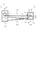
- FIG. 1 is a top view of a state in which a display device according to an embodiment of the present invention is extended.
- 2 is a cross-sectional view taken along line A1-A2 of FIG.
- the display device 10 includes a display panel 100, a storage body 200, a power supply unit 300, and a drawer structure 400.
- the display panel 100 has flexibility. That is, a flexible base material such as a resin base material is used as the base material of the array substrate and the counter substrate of the display panel 100.
- the upper surface of the display panel 100 is a display surface 101.
- a surface opposite to the display surface 101 is referred to as a back surface 103.
- the display surface 101 is a surface on which the display panel 100 displays an image.
- a display area 105 shown in FIG. 1 is an area for displaying an image in the display panel 100.
- the display device 10 is a top emission type organic EL display device
- the counter substrate side is the display surface 101.
- the array substrate side is the display surface 101.
- the display device 10 is a liquid crystal display device
- the substrate surface opposite to the backlight with respect to the transistors provided in the display device 10 is the display surface 101.
- the drawer structure 400 may be provided with a backlight or a light guide plate.
- the display surface 101 is a flat surface.
- a protrusion 110 is provided on the back surface 103 side.
- the protrusion 110 provides unevenness on the surface of the display panel 100 on the back surface 103 side together with the back surface 103.
- a drive circuit 120 is provided in an area stored in the power supply unit 300.
- the drive circuit 120 is a circuit that drives a pixel circuit provided in the display panel 100.
- the storage body 200 has a casing 210 and a winding shaft 220.
- the housing 210 is provided with an opening 211.
- the display panel 100 and the drawer structure 400 enter and exit the storage body 200 through the opening 211.
- the take-up shaft 220 is rotatably provided inside the housing 210.
- the first end 107 of the display panel 100 is fixed to the panel fixing part 221 of the winding shaft 220. With this configuration, the display panel 100 is wound around the winding shaft 220.
- the power supply unit 300 includes a housing 310, a panel fixing unit 320, a control circuit 330, and a connection line 340.
- the housing 310 is provided with openings 311 and 313.
- the display panel 100 passes through the opening 311 and enters the housing 310.
- the drawer structure 400 passes through the opening 313 and enters the housing 310, and is fixed to the housing 310.
- the panel fixing unit 320 and the control circuit 330 are fixed inside the housing 310.
- the panel fixing unit 320 fixes the second end 109 of the display panel 100. That is, the power supply unit 300 moves with the display panel 100.
- the control circuit 330 is connected to the display panel 100 via a connection line 340.
- the control circuit 330 controls the drive circuit 120 and supplies power to the display panel 100 and the drive circuit 120.
- the drawer structure 400 is a member that can be expanded and contracted according to the winding and stretching operations of the display panel 100.
- the drawer structure 400 is a support member that maintains the rigidity of the display device 10 in a state where the display panel 100 is wound up and extended.
- a member having a telescopic structure in which components are combined in a nested manner, such as a rod antenna, can be used.
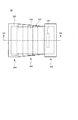
- FIG. 3 is a top view showing a state where the display device according to the embodiment of the present invention is being wound.
- 4 is a cross-sectional view taken along line A3-A4 of FIG.
- the first end 107 of the display panel 100 is connected to the take-up shaft 220, and the second end 109 of the display panel 100 is connected to the panel fixing part 320. Therefore, when the winding shaft 220 rotates clockwise, the display panel 100 is wound around the winding shaft 220, and the power supply unit 300 approaches the storage body 200 as the display panel 100 moves.
- the display panel 100 is wound in a state where the display surface 101 is closer to the winding shaft 220 than the back surface 103. That is, the display panel 100 is wound so that the display surface 101 is on the inside. Therefore, the display surface 101 of the wound display panel 100 comes into contact with the protrusion 110 provided on the back surface 103 of the display panel 100 that has already been wound. Note that when the display panel 100 is wound up, the drawer structure 400 supports the display panel 100 while contracting.
- FIG. 5A is a cross-sectional view showing a state in which display panels overlap each other in a state in which the display device according to an embodiment of the present invention is wound, and a perspective view showing the shape of protrusions provided on the back surface of the display panel FIG.
- the upper side is the winding shaft 220 side (inner side).
- the display surface 101-1 of the outer display panel 100-1 is in contact with the protrusion 110-2 provided on the back surface 103-2 of the inner display panel 100-2. That is, a gap is formed between the back surface 103-2 and the display surface 101-1.
- the contact between the back surface 103-2 and the display surface 101-1 is suppressed, and thus the sticking of both can be suppressed.
- the display panel 100 can be smoothly stretched from the wound state, mechanical destruction of the display panel 100 that occurs when the back surface 103-2 is peeled off from the display surface 101-1, and static electricity Can be suppressed.
- FIG. 5A illustrates the configuration in which the shape of the protrusion 110 is hemispherical, it is not limited to this configuration.
- the protrusion 110 may have a cylindrical shape as shown in FIG. 5B, or may have a truncated cone shape as shown in FIG. 5C.
- the protrusions 110 are arranged with regularity, these protrusions 110 are arranged so that the interval S is provided.
- interval S is a space
- the interval S, the thickness T, the width W, and the height H are as follows. It is preferable to satisfy the following condition. Of the following three conditions, at least two conditions may be satisfied. When these parameters satisfy the following conditions, the contact between the back surface 103-2 and the display surface 101-1 can be suppressed. As a result, the display panel 100 can be smoothly extended from the wound state. 0.05T ⁇ H ⁇ 0.2T H ⁇ W ⁇ 10H W ⁇ S ⁇ 10W
- the protrusion 110 may be an insulating material, may be a conductive material, or may be laminated. By using a conductive material as the protrusion 110, it is possible to suppress the generation of static electricity due to friction between the protrusion 110 and the display surface 101 of the display panel 100. Therefore, when the insulating material and the conductive material are stacked as the protrusion 110, it is preferable that the protrusion 110 be stacked so that the conductive material is on the surface.
- the protrusion 110 may be an organic material, an inorganic material, or a laminate thereof. When an organic material is also used as the protrusion 110, an elastic body may be used.
- the protrusion 110 By using an organic material (particularly, an elastic body) as the protrusion 110, it is possible to suppress the display surface 101 from being damaged due to contact between the protrusion 110 and the display surface 101. In other words, when the organic material and the inorganic material are stacked as the protrusion 110, it is preferable to stack the organic material on the surface.
- an organic material particularly, an elastic body
- the protrusion 110 may be formed by a printing method or an ink jet method. Alternatively, the protrusion 110 may be formed by processing a film formed on the back surface 103 of the display panel 100.
- the protrusion 110 provided on the back surface 103 side is illustrated as the structure that provides unevenness on the back surface 103 side of the display panel 100.
- unevenness may be provided on the back surface 103 side by using another structure.
- FIG. 6 is a cross-sectional view of a display panel of a display device according to an embodiment of the present invention.
- FIG. 6 illustrates a first pixel 131 and a second pixel 133 as a configuration of the pixel unit 130.
- the display panel 100 includes a functional circuit layer 152 and an electro-optical layer 154 on the first surface side of the substrate 150.
- the functional circuit layer 152 includes a transistor 140.
- a functional circuit layer 152 is configured by a combination of the plurality of transistors 140.
- the transistor 140 has a structure in which a semiconductor layer 141, a gate insulating layer 143, and a gate electrode 147 are stacked.
- the semiconductor layer 141 is formed using amorphous silicon, polycrystalline silicon, an oxide semiconductor, or the like.
- the source / drain wiring 149 is provided on the upper layer of the gate electrode 147 with the first insulating layer 144 interposed therebetween.
- a second insulating layer 145 functioning as a planarization layer is provided on the source and drain wirings 149.
- the first insulating layer 144 is formed of an inorganic insulating material such as silicon oxide or silicon nitride.
- the second insulating layer 145 is formed of an organic insulating material such as polyimide or acrylic.
- the electro-optic layer 154 is disposed on the upper side of the functional circuit layer 152.
- the electro-optic layer 154 includes an organic EL element 142 as a display element.
- the organic EL element 142 has a structure in which a first electrode 171, an organic layer 173, and a second electrode 175 are stacked.
- the organic EL element 142 is covered with a protective layer 156.
- the organic EL element 142 is electrically connected to the transistor 140.
- the transistor 140 controls light emission of the organic EL element 142.
- Light emitted from the organic EL element 142 is emitted through the protective layer 156.
- the surface of the protective layer 156 is the display surface 101.
- the electromagnetic shield 160 is disposed on the back surface 103. In other words, the electromagnetic shield 160 is disposed on the second surface side facing the first surface of the substrate 150.
- the electromagnetic shield 160 has conductivity.
- the electromagnetic shield 160 can be provided in various forms. For example, a metal film provided on the second surface of the substrate 150 can be used as the electromagnetic shield 160.
- a metal film such as aluminum, titanium, molybdenum, tungsten, and chromium, or a transparent conductive film such as ITO can be used.
- the electromagnetic shield 160 can be formed using a vacuum deposition method or a sputtering method.
- the configuration of the electromagnetic shield 160 may be a single layer or a configuration in which a plurality of layers are stacked.
- the metal thin film By providing the metal thin film on the second surface of the substrate 150 of the display panel 100, the metal thin film can be wound together with the display panel 100. As another form, it can be set as the electromagnetic shield 160 by providing a metal film in one surface of the base material by an insulating film etc., and arrange
- Electromagnetic noise generated in the functional circuit layer 152 is also radiated to the electro-optic layer 154 side.
- the second electrode 175 of the organic EL element 142 is disposed on substantially the entire surface of the pixel portion. Since the second electrode 175 is held at a constant potential, it also functions as the electromagnetic shield 160.
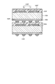
- FIG. 7 is a cross-sectional view illustrating a state in which display panels overlap each other in a state in which the display device according to the embodiment of the present invention is wound.
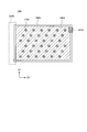
- FIG. 8 is a plan view showing the configuration of the back electrode and the protrusion provided on the back surface of the display device according to the embodiment of the present invention.
- the display device 10A of the present embodiment is similar to the display device 10 of the first embodiment, but is different from the display device 10 in that a conductive film 180A is provided between the display panel 100A and the protrusion 110A. Is different.
- the conductive film 180A is provided on the back surface 103A (103A-1 and 103A-2) of the display panel 100A (100A-1 and 100A-2).
- the protrusion 110A is provided on the surface of the conductive film 180A.
- the protrusion 110A of this embodiment is conductive. That is, the protrusion 110A is electrically connected to the conductive film 180A.
- the protrusion 110A may be insulative.
- the conductive film 180A is formed over the entire area of the display panel 100A.
- a connecting portion 181A is provided at the end of the display panel 100A.
- the connecting portion 181A is connected to the conductive film 180A on the back surface 103A side, and is connected to the drive circuit 120 or the control circuit 330 shown in FIG. 2 on the display surface 101A.
- the connection portion 181A supplies the potential provided from the drive circuit 120 or the control circuit 330 to the conductive film 180A.
- the potential supplied to the conductive film 180A may be constant or may vary. Note that in the case where it is not necessary to supply a potential to the conductive film 180A, the connection portion 181A is not necessarily provided. That is, the potential of the conductive film 180A may be floating.
- the protrusions 110A are regularly arranged.
- the direction in which the winding shaft 220A extends is defined as a first direction D1
- the direction orthogonal to the first direction D1 is defined as a second direction D2.
- the protrusions 110A are arranged on a straight line extending in the second direction D2.
- the protrusions 110A are arranged at an equal pitch in the second direction D2.
- the linear arrangement of the protrusions 110A is aligned in the first direction D1 while the positions of the protrusions 110A are shifted in the second direction D2.
- FIG. 1 the direction in which the winding shaft 220A extends
- the direction orthogonal to the first direction D1 is defined as a second direction D2.
- the protrusions 110A are arranged on a straight line extending in the second direction D2.
- the protrusions 110A are arranged at an equal pitch in the second direction D2.
- the linear arrangement of the protrusions 110A is aligned in the
- the protrusion 110A is arranged in an oblique direction with respect to the first direction D1.
- the arrangement of the protrusions 110A in the second direction D2 may not be equal pitch.
- the amount of deviation of the protrusion 110A adjacent to the first direction D1 in the second direction D2 may not be constant.
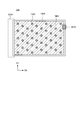
- the protrusions 110A may be arranged at an equal pitch on a straight line extending in the first direction D1. In FIG. 9, the linear arrangement of the protrusions 110A is aligned in the second direction D2 while the positions of the protrusions 110A are shifted in the first direction D1.
- the conductive film 180A is provided between the display panel 100A and the protrusion 110A, when the display device 10A is extended from the rolled-up state, the display surface 101A of the display panel 100A and the protrusion Even if static electricity is generated between the object 110A and the charge, the charge moves to the conductive film 180A through the protrusion 110A. Therefore, electrostatic breakdown due to the generated static electricity can be suppressed. Note that since the conductive film 180A is provided, part of the generated static electricity moves to the conductive film 180A even when the protrusion 110A is insulative, so that an effect of suppressing electrostatic breakdown can be obtained. it can. Further, as shown in FIG.
- the display panel 10A is displayed at the same timing when the display device 10A is extended from the wound state. Since the number of protrusions 110A that are separated from the display surface 101A of 100A can be reduced, generation of static electricity can be suppressed and electrostatic breakdown can be suppressed.
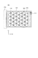
- the conductive films 180B to 180E are patterned into various shapes, unlike the planar shape of the conductive film 180A in FIG. 10 to 13 are each a plan view showing the configuration of the back electrode and the protrusion provided on the back surface of the display device according to the modification of the embodiment of the present invention.
- the conductive film 180B shown in FIG. 10 has an opening 183B.
- the opening 183B penetrates the conductive film 180B and exposes the back surface 103B of the display panel 100B.
- the openings 183B have a rhombus planar shape, and are arranged so that the rhombus sides of the adjacent openings 183B face each other.
- the conductive film 180B is patterned in a mesh shape.
- the protrusion 110B is disposed on the patterned conductive film 180B.
- the protrusion 110B of this embodiment is conductive. That is, the protrusion 110B is electrically connected to the mesh-like conductive film 180B. In the example shown in FIG.
- the protrusion 110B is disposed at a position adjacent to each apex of the rhombus of the opening 183B, that is, at the intersection of the linear conductive film 180B, but is not limited to this configuration.
- the protrusion 110B may be disposed on the conductive film 180B other than the above, or may be disposed in the opening 183B.
- the protrusion 110B may be insulative.
- the conductive film 180C shown in FIG. 11 has a hexagonal opening 183C.
- the opening 183C penetrates the conductive film 180C similarly to the opening 183B, and exposes the back surface 103C of the display panel 100C.
- the openings 183C are arranged so that the sides of the hexagon face each other. In other words, the conductive film 180C is patterned into a honeycomb shape. Note that the protrusion 110C is disposed on the conductive film 180C as in FIG.
- the openings 183B and 183C are formed in the conductive films 180B and 180C, so that the flexibility of the display panels 100B and 100C can be improved. That is, the display devices 10B and 10C that are easy to wind can be realized.
- the conductive film 180D shown in FIG. 12 has an opening 183D having a length in the first direction D1.
- the opening 183D penetrates the conductive film 180D similarly to the opening 183B, and exposes the back surface 103D of the display panel 100D.
- the openings 183D are arranged in the second direction D2.
- the protrusion 110D is disposed both on the conductive film 180D and in the opening 183D. That is, some of the protrusions 110D are electrically connected to the conductive film 180D, and the other part of the protrusions 110D are insulated from the conductive film 180D.
- the protrusion 110D disposed in the opening 183D is provided on the back surface 103D of the display panel 100D. Therefore, the position of the top of the protrusion 110D in the opening 183D is the protrusion on the conductive film 180D. It is lower than the position of the top of the object 110D (close to the display panel 100D).
- the protrusion 110D is provided on both the conductive film 180D and the opening 183D, for example, the display device 10D is strongly wound, and a strong pressure is applied to the protrusion 110D on the conductive film 180D. Even if the protrusion 110D is crushed, the interval between the overlapping display panels 100D can be maintained by the protrusion 110D in the opening 183D.
- a conductive film 180E shown in FIG. 13 has an opening 183E having the same shape as the opening 183B provided in the conductive film 180B of FIG.
- the protrusion 110E is not disposed on the conductive film 180E, but is disposed only in the opening 183E. That is, the protrusion 110E is insulated from the conductive film 180E.
- FIG. 13 illustrates the configuration in which the protrusions 110E are disposed only in some of the openings 183E among the plurality of openings 183E, the protrusions 110E may be disposed in all the openings 183E.
- the protrusion 110E It may be difficult to form the protrusion 110E low depending on the formation method.
- the protrusion 110E is formed by an ink jet method, there is a limit to reducing the height of the protrusion 110E with respect to the diameter in plan view.
- the height of the protrusion 110E can be reduced by the thickness of the conductive film 180E.
- ⁇ Third Embodiment> The configuration of the display device 10F according to an embodiment of the present invention will be described with reference to FIGS.
- a display device 10F in which a touch sensor 500F is provided on the display surface 101F of the display panel 100F will be described.
- FIG. 14 is a plan view showing a configuration of a touch sensor electrode provided on the surface of the display device according to the embodiment of the present invention.
- the touch sensor 500F is provided in the display area 105F of the display panel 100F.
- the touch sensor 500F includes a sensor electrode 510F (detection electrode Rx and drive electrode Tx).
- the sensor electrodes 510F are arranged in a matrix so as not to overlap each other in plan view.
- Each of the plurality of sensor electrodes 510F is connected to the terminal portion 501F via a wiring.
- a touch sensor 500F illustrated in FIG. 14 is a capacitive touch sensor.
- the touch sensor 500F is a self-capacitance type touch sensor. That is, the touch sensor 500F detects the touch of the human body by detecting the capacitance between the sensor electrode 510F and the human body (fingertip).
- FIG. 15 is a cross-sectional view showing a state in which display panels overlap each other in a state in which the display device according to an embodiment of the present invention is wound up.
- a touch sensor 500F is provided on the display surface 101F of the display panel 100F.
- a sensor electrode 510F is provided on the display surface 101F, and a protective film 520F that covers the sensor electrode 510F is provided thereon.
- the surface of the protective film 520F is flat. In the state where the display panel 100F is wound up, the protective film 520F and the protrusion 110F come into contact with each other.
- the protrusion 110F is conductive, a potential can be supplied to the protrusion 110F through the conductive film 180F.
- a capacitance is formed between them.
- the amount of winding can be determined by detecting the touch of the protrusion 110F.
- FIG. 16 is a plan view showing the configuration of the back electrode and the protrusion provided on the back surface of the display device according to the embodiment of the present invention.
- FIG. 17 is a cross-sectional view illustrating a state in which display panels overlap each other in a state in which the display device according to the embodiment of the present invention is wound up.
- the conductive film 180G is in contact with the display surface 101G of the display panel 100G when the display panel 100G is wound up.
- the opening 183G is provided in the conductive film 180G, a gap is formed in a region corresponding to the opening 183G. That is, in the present embodiment, the conductive film 180G provided with unevenness by the opening 183G is used as the structure that provides unevenness on the back surface 103G side of the display panel 100G.
- the opening 183G penetrates the conductive film 180G, but unevenness that does not penetrate the conductive film 180G may be provided instead of the opening 183G.
- An insulating film may be used instead of the conductive film 180G.
- the same effect as that of the first embodiment can be obtained by forming a film having irregularities on the back surface 103G. Can do.
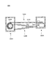
- FIG. 18 is a cross-sectional view of a state in the middle of winding up the display device according to the embodiment of the present invention.
- the display device 10H shown in FIG. 18 is similar to the display device 10 shown in FIG. 4, but the direction in which the display panel 100H is wound around the winding shaft 220H is different. Specifically, in a state where the display panel 100H is wound around the winding shaft 220, the protrusion 110H is positioned closer to the winding shaft 220H (inside) than the display panel 100H.
- the protrusion 110H exists between the display panel 100H closest to the winding shaft 220H and the winding shaft 220H. Therefore, it is possible to suppress the display panel 100H from sticking to the take-up shaft 220H. As a result, the display device 10H can be smoothly extended from the wound state to the end. Thereby, mechanical destruction of the display panel 100H and generation of static electricity can be suppressed.
Landscapes
- Physics & Mathematics (AREA)
- General Physics & Mathematics (AREA)
- Engineering & Computer Science (AREA)
- Theoretical Computer Science (AREA)
- Devices For Indicating Variable Information By Combining Individual Elements (AREA)
- Chemical & Material Sciences (AREA)
- Crystallography & Structural Chemistry (AREA)
- Electroluminescent Light Sources (AREA)
Abstract
表示装置は、可撓性を有し、表示面を有するパネルと、前記パネルに対して前記表示面とは反対側の裏面に離散的に設けられた構造体と、を備える。前記構造体は、前記裏面から突出する突起物であってもよい。前記裏面と前記突起物との間に導電性を有する導電膜が設けられていてもよい。前記突起物は導電性を有していてもよい。前記導電膜は、前記裏面の一部を露出する開口を有していてもよい。前記導電膜は、メッシュ状であってもよい。
Description
本発明の実施形態の一つは、表示装置に関する。特に、本発明の実施形態の一つは、巻き取り可能なフレキシブル表示装置に関する。
フレキシブル表示装置は、携帯可能であり、巻き取り可能な表示装置、及びスクリーン状の大画面表示装置など、幅広く応用されることが期待されている。フレキシブル表示装置は軽量かつ収納性に優れた次世代表示装置として実現されることが強く望まれている。現在、表示装置のフレキシブル化の研究開発は盛んに行われており、有機発光素子(Organic Light-Emitting Diode;OLED)及び電子ペーパーなどの表示装置のフレキシブル化だけでなく、液晶表示装置(Liquid Crystal Display Device;LCD)のフレキシブル化の研究開発が進められている。
フレキシブル表示装置は、樹脂基板などの可撓性を有する基板(以下、「可撓性基板」という)の上に、トランジスタや容量など、表示装置を構成する機能素子が設けられた構成を有している。例えば、特許文献1及び2には、可撓性基板の上にこれらの機能性素子が設けられた構造が記載されている。これらの特許文献では、可撓性基板を折り曲げることによる機能性素子への影響を緩和させるための構造が記載されている。
フレキシブル表示装置を巻き取る場合、当該表示装置の表面と裏面とが接触する状態で巻き取られる。表示装置が巻き取られた状態において、表示装置の表面と裏面とが平坦である場合、互いに接触した表面と裏面とが貼り付いてしまう。このように表示装置の表面と裏面とが貼り付いた状態で、巻き取られた状態の表示装置を引き延ばすと、滑らかに引き延ばすことができない。さらに、表示装置を引き延ばす際に、貼り付いた箇所が強制的に引き剥がされるため、表示装置が機械的に破壊される、又は剥離の際に発生する静電気によって機能素子が破壊されてしまう。
特許文献1及び2では、基板の上面方向に突出した構造体が設けられた表示装置又は半導体装置が記載されている。しかし、表示装置では、上面側から画像を表示させるため、基板の上面に上記のような構造体を設けると、画像の表示性能が低下してしまう。さらに、表示装置の上面側にタッチセンサを設ける場合があるため、表示装置の上面に上記のような構造体が設けられていると、タッチセンサを設けることができない、又はタッチセンサを設けるためにさらに表示装置の表面を平坦化する必要がある。
本発明は上記実情を鑑みてなされた発明であり、本発明の実施形態の一つは、巻き取り可能なフレキシブル表示装置を、巻き取られた状態から滑らかに引き延ばすことができる表示装置を提供することを課題の一つとする。
本発明の一実施形態に係る表示装置は、可撓性を有し、表示面を有するパネルと、前記パネルに対して前記表示面とは反対側の裏面に離散的に設けられた構造体と、を備える。
本発明の一実施形態に係る表示装置は、可撓性を有し、表示面を有するパネルと、前記パネルに対して前記表示面とは反対側の裏面に設けられ、複数の開口が設けられた膜と、を備える。
以下に、本発明の各実施の形態について、図面を参照しつつ説明する。なお、開示はあくまで一例にすぎない。当業者が、発明の主旨を保ちつつ適宜変更することで、容易に想到し得る構成は、当然に本発明の範囲に含有される。また、図面は説明をより明確にするため、実際の態様に比べ、各部の幅、厚さ、形状等が模式的に表される場合がある。しかし、図示された形状はあくまで一例であって、本発明の解釈を限定するものではない。また、本明細書と各図において、既出の図に関して前述したものと同様の要素には、同一の符号の後にアルファベットを付して、詳細な説明を適宜省略することがある。
本発明の各実施の形態において、トランジスタが配置されたアレイ基板からアレイ基板に対向する対向基板に向かう方向を上または上方という。逆に、対向基板からアレイ基板に向かう方向を下または下方という。このように、説明の便宜上、上方または下方という語句を用いて説明する。しかし、例えば、アレイ基板と対向基板との上下関係が図示と逆になるように配置されてもよい。また、以下の説明で、例えばアレイ基板上の対向基板という表現は、上記のようにアレイ基板と対向基板との上下関係を説明しているに過ぎず、アレイ基板と対向基板との間に他の部材が配置されていてもよい。
表示パネルにおける「内側」及び「外側」とは、2つの部位における、表示部を基準とした相対的な位置関係を示す。すなわち、「内側」とは、一方の部位に対して相対的に表示部に近い側を指す。一方、「外側」とは、一方の部位に対して相対的に表示部から遠い側を指す。ただし、ここで言う「内側」および「外側」の定義は、表示装置を折り曲げ又は巻き取られていない状態における位置関係を示す。
「表示装置」とは、電気光学層を用いて映像を表示する構造体を指す。例えば、表示装置という用語は、電気光学層を含む表示パネルを指す場合もあり、又は表示セルに対して他の光学部材(例えば、偏光部材、バックライト、タッチパネル等)を装着した構造体を指す場合もある。ここで、「電気光学層」には、技術的な矛盾が生じない限り、液晶層、エレクトロルミネセンス(EL)層、エレクトロクロミック(EC)層、電気泳動層が含まれ得る。したがって、後述する実施形態では、表示装置として、EL層を含む有機EL表示装置を例示して説明するが、本発明は、上述した他の電気光学層を含む表示装置に適用することができる。
本明細書において「αはA、BまたはCを含む」、「αはA,BおよびCのいずれかを含む」、「αはA,BおよびCからなる群から選択される一つを含む」、といった表現は、特に明示が無い限り、αがA~Cの複数の組み合わせを含む場合を排除しない。さらに、これらの表現は、αが他の要素を含む場合も排除しない。
なお、以下の各実施形態は、技術的な矛盾を生じない限り、互いに組み合わせることができる。
〈第1実施形態〉
図1~図6を用いて、本発明の一実施形態及びその変形例に係る表示装置について説明する。なお、本実施形態では、表示パネル100が巻き取り軸220によって巻き取られる構成を例示したが、本発明は表示パネル100が手動で丸められるようなフレキシブル表示装置に適用することもできる。
図1~図6を用いて、本発明の一実施形態及びその変形例に係る表示装置について説明する。なお、本実施形態では、表示パネル100が巻き取り軸220によって巻き取られる構成を例示したが、本発明は表示パネル100が手動で丸められるようなフレキシブル表示装置に適用することもできる。
[表示装置10の構成]
図1及び図2を用いて、本発明の一実施形態に係る表示装置10の構成について説明する。図1は、本発明の一実施形態に係る表示装置が引き延ばされた状態の上面図である。図2は、図1のA1-A2断面図である。図1及び図2に示すように、表示装置10は、表示パネル100、格納体200、電源供給部300、及び引き出し構造体400を有している。
図1及び図2を用いて、本発明の一実施形態に係る表示装置10の構成について説明する。図1は、本発明の一実施形態に係る表示装置が引き延ばされた状態の上面図である。図2は、図1のA1-A2断面図である。図1及び図2に示すように、表示装置10は、表示パネル100、格納体200、電源供給部300、及び引き出し構造体400を有している。
表示パネル100は可撓性を有する。つまり、表示パネル100のアレイ基板及び対向基板の基材として、樹脂基材のように可撓性を有する基材が用いられる。表示パネル100は、その上面が表示面101である。表示面101とは反対側の面を裏面103という。表示面101は表示パネル100が画像を表示する面である。図1に示す表示領域105は表示パネル100のうち画像を表示する領域である。
例えば、表示装置10がトップエミッション型の有機EL表示装置であれば対向基板側が表示面101である。表示装置10がボトムエミッション型の有機EL表示装置であれば、アレイ基板側が表示面101である。表示装置10が液晶表示装置の場合、表示装置10に設けられたトランジスタに対してバックライトとは反対側の基板表面が表示面101である。表示装置10が液晶表示装置の場合、引き出し構造体400にバックライトや導光板を設けてもよい。
表示面101は平坦な面である。裏面103側には突起物110が設けられている。突起物110は、裏面103と共に表示パネル100の裏面103側の表面に凹凸を提供する。表示面101側には、電源供給部300に格納された領域に駆動回路120が設けられている。駆動回路120は、表示パネル100に設けられた画素回路を駆動する回路である。
格納体200は、筐体210及び巻き取り軸220を有している。筐体210には開口部211が設けられている。開口部211を通過して表示パネル100及び引き出し構造体400が格納体200を出入りする。巻き取り軸220は筐体210の内部に回動可能に設けられている。表示パネル100の第1端部107は巻き取り軸220のパネル固定部221に固定されている。この構成によって、表示パネル100は巻き取り軸220に巻き付けられている。
電源供給部300は、筐体310、パネル固定部320、制御回路330、及び接続線340を有している。筐体310には開口部311、313が設けられている。表示パネル100は開口部311を通過して筐体310の内部に入り込んでいる。引き出し構造体400は開口部313を通過して筐体310の内部に入り込み、筐体310に固定されている。パネル固定部320及び制御回路330は筐体310の内部に固定されている。パネル固定部320は表示パネル100の第2端部109を固定する。つまり、電源供給部300は表示パネル100と共に移動する。制御回路330は接続線340を介して表示パネル100に接続されている。制御回路330は、駆動回路120を制御し、表示パネル100及び駆動回路120に電源を供給する。
引き出し構造体400は、表示パネル100の巻き取り及び引き延ばしの動作に応じて伸縮可能な部材である。引き出し構造体400は、表示パネル100が巻き取られた状態及び引き延ばされた状態において、表示装置10の剛性を維持する支持部材である。引き出し構造体400として、例えばロッドアンテナのような、入れ子式に部品を組み合わせた伸縮可能な構造の部材を用いることができる。
[表示装置10の巻き取り動作]
図3及び図4を用いて、表示装置10の巻き取り動作について説明する。図3は、本発明の一実施形態に係る表示装置が巻き取られている途中の状態の上面図である。図4は、図3のA3-A4断面図である。
図3及び図4を用いて、表示装置10の巻き取り動作について説明する。図3は、本発明の一実施形態に係る表示装置が巻き取られている途中の状態の上面図である。図4は、図3のA3-A4断面図である。
図2に示すように、表示パネル100の第1端部107が巻き取り軸220に接続され、表示パネル100の第2端部109がパネル固定部320に接続されている。そのため、巻き取り軸220が時計回りに周回すると表示パネル100が巻き取り軸220に巻き取られ、表示パネル100の移動に伴い電源供給部300が格納体200に近づく。表示パネル100は、表示面101が裏面103よりも巻き取り軸220に近い状態で巻き取られる。つまり、表示パネル100は表示面101が内側になるように巻き取られる。したがって、巻き取られた表示パネル100の表示面101は、既に巻き取られている表示パネル100の裏面103に設けられた突起物110と接触する。なお、表示パネル100が巻き取られる際に、引き出し構造体400は収縮しながら表示パネル100を支持する。
[巻き取られた表示パネル100の重畳状態]
図5Aを用いて、巻き取られた状態における表示パネル100の重畳状態を説明する。図5Aは、本発明の一実施形態に係る表示装置が巻き取られた状態において、表示パネル同士が重なり合っている状態を示す断面図及び表示パネルの裏面に設けられた突起物の形状を示す斜視図である。なお、図5Aにおいて、上方が巻き取り軸220側(内側)である。図5Aに示すように、外側の表示パネル100-1の表示面101-1は、内側の表示パネル100-2の裏面103-2に設けられた突起物110-2と接触する。つまり、裏面103-2と表示面101-1との間に間隙が形成される。上記の構成によって、裏面103-2と表示面101-1との接触が抑制されるため、両者が貼り付くことを抑制することができる。その結果、表示パネル100を巻き取られた状態から滑らかに引き延ばすことができるため、裏面103-2と表示面101-1との剥離の際に発生する表示パネル100の機械的な破壊、及び静電気の発生を抑制することができる。
図5Aを用いて、巻き取られた状態における表示パネル100の重畳状態を説明する。図5Aは、本発明の一実施形態に係る表示装置が巻き取られた状態において、表示パネル同士が重なり合っている状態を示す断面図及び表示パネルの裏面に設けられた突起物の形状を示す斜視図である。なお、図5Aにおいて、上方が巻き取り軸220側(内側)である。図5Aに示すように、外側の表示パネル100-1の表示面101-1は、内側の表示パネル100-2の裏面103-2に設けられた突起物110-2と接触する。つまり、裏面103-2と表示面101-1との間に間隙が形成される。上記の構成によって、裏面103-2と表示面101-1との接触が抑制されるため、両者が貼り付くことを抑制することができる。その結果、表示パネル100を巻き取られた状態から滑らかに引き延ばすことができるため、裏面103-2と表示面101-1との剥離の際に発生する表示パネル100の機械的な破壊、及び静電気の発生を抑制することができる。
[突起物110の形状]
図5Aでは、突起物110の形状が半球状である構成を例示したが、この構成に限定されない。例えば、突起物110は図5Bに示すように円柱状であってもよく、図5Cに示すように円錐台形状であってもよい。突起物110が規則性を持って配置される場合、これらの突起物110は間隔Sが設けられるように配置される。なお、間隔Sは、規則的に配置された複数の突起物110のうち、隣接する突起物110の間隔が最も短い突起物110間の間隔である。また、表示パネル100の厚さT、突起物110の平面視における最大の幅W、及び突起物110の高さHを用いると、間隔S、厚さT、幅W、及び高さHは以下の条件を満たすことが好ましい。なお、以下の3つの条件のうち、少なくとも2つ以上の条件を満たせばよい。これらのパラメータが以下の条件を満たすことで、裏面103-2と表示面101-1との接触を抑制することができる。その結果、表示パネル100を巻き取られた状態から滑らかに引き延ばすことができる。
0.05T≦H≦0.2T
H≦W≦10H
W≦S≦10W
図5Aでは、突起物110の形状が半球状である構成を例示したが、この構成に限定されない。例えば、突起物110は図5Bに示すように円柱状であってもよく、図5Cに示すように円錐台形状であってもよい。突起物110が規則性を持って配置される場合、これらの突起物110は間隔Sが設けられるように配置される。なお、間隔Sは、規則的に配置された複数の突起物110のうち、隣接する突起物110の間隔が最も短い突起物110間の間隔である。また、表示パネル100の厚さT、突起物110の平面視における最大の幅W、及び突起物110の高さHを用いると、間隔S、厚さT、幅W、及び高さHは以下の条件を満たすことが好ましい。なお、以下の3つの条件のうち、少なくとも2つ以上の条件を満たせばよい。これらのパラメータが以下の条件を満たすことで、裏面103-2と表示面101-1との接触を抑制することができる。その結果、表示パネル100を巻き取られた状態から滑らかに引き延ばすことができる。
0.05T≦H≦0.2T
H≦W≦10H
W≦S≦10W
突起物110は、絶縁性を有する材料であってもよく、導電性を有する材料であってもよく、これらを積層させてもよい。突起物110として、導電性を有する材料を用いることで、突起物110と表示パネル100の表示面101との間の摩擦によって静電気が発生することを抑制できる。したがって、突起物110として、絶縁性を有する材料と導電性を有する材料とを積層させる場合、導電性を有する材料が表面になるように積層させることが好ましい。突起物110は、有機材料であってもよく、無機材料であってもよく、これらを積層させてもよい。突起物110として有機材料も用いる場合、弾性体を用いてもよい。突起物110として有機材料(特に弾性体)を用いることで、突起物110と表示面101との接触によって、表示面101に傷が付くことを抑制することができる。つまり、突起物110として、有機材料と無機材料とを積層させる場合、有機材料が表面になるように積層させることが好ましい。
突起物110は、印刷法で形成してもよく、インクジェット法で形成してもよい。又は、表示パネル100の裏面103に形成した膜を加工して突起物110を形成してもよい。
本実施形態では、表示パネル100の裏面103側に凹凸を提供する構造体として、裏面103側に設けられた突起物110を例示したが、他の実施形態でも説明するように、突起物110の代わりに他の構造体を用いることで裏面103側に凹凸を提供してもよい。
[表示パネル100の構造]
図6を用いて、本実施形態に用いられる表示パネル100の一例を説明する。図6は、本発明の一実施形態に係る表示装置の表示パネルの断面図である。図6には画素部130の構成として第1画素131及び第2画素133が例示されている。表示パネル100は、基材150の第1面側に機能回路層152及び電気光学層154を有している。機能回路層152はトランジスタ140を含む。複数のトランジスタ140の組み合わせによって機能回路層152が構成されている。
図6を用いて、本実施形態に用いられる表示パネル100の一例を説明する。図6は、本発明の一実施形態に係る表示装置の表示パネルの断面図である。図6には画素部130の構成として第1画素131及び第2画素133が例示されている。表示パネル100は、基材150の第1面側に機能回路層152及び電気光学層154を有している。機能回路層152はトランジスタ140を含む。複数のトランジスタ140の組み合わせによって機能回路層152が構成されている。
図6の挿入図(A)に示すように、トランジスタ140は、半導体層141、ゲート絶縁層143、ゲート電極147が積層された構造を有する。半導体層141は、非晶質シリコン、多結晶シリコン、又は酸化物半導体等で形成される。ソース及びドレイン配線149は、第1絶縁層144を介してゲート電極147の上層に設けられる。ソース及びドレイン配線149の上層には平坦化層として機能する第2絶縁層145が設けられる。第1絶縁層144は、酸化シリコン、窒化シリコン等の無機絶縁材料で形成される。第2絶縁層145はポリイミド、アクリル等の有機絶縁材料で形成される。
機能回路層152の上層側に電気光学層154が配置される。電気光学層154は表示素子として有機EL素子142を含む。図6の挿入図(B)に示すように、有機EL素子142は、第1電極171、有機層173、及び第2電極175が積層された構造を有する。有機EL素子142は保護層156で覆われている。第1画素131及び第2画素133のそれぞれにおいて、有機EL素子142は、トランジスタ140と電気的に接続される。トランジスタ140は有機EL素子142の発光を制御する。有機EL素子142の発光は保護層156を通して出射される。この場合、保護層156の表面が表示面101である。
電磁シールド160は裏面103に配置される。換言すると、電磁シールド160は、基材150の第1面に対向する第2面の側に配置される。電磁シールド160は、導電性を有する。電磁シールド160は、様々な形態で設けることが可能である。例えば、基材150の第2面に設けられた金属膜を電磁シールド160として用いることができる。電磁シールド160として、アルミニウム、チタン、モリブデン、タングステン、及びクロム等の金属膜、又はITO等の透明導電膜を用いることができる。電磁シールド160は、真空蒸着法やスパッタリング法を用いて形成することができる。電磁シールド160の構成は、一層であってもく、複数層を積層した構成であってもよい。金属の薄膜を、表示パネル100の基材150の第2面に設けることで、当該金属の薄膜を表示パネル100と共に巻き取ることができる。他の形態として、絶縁フィルム等による基材の一面に金属膜を設け、これを基材150の第2面側に配置することで、電磁シールド160とすることができる。
機能回路層152で発生する電磁ノイズは、電気光学層154側にも放射される。しかし、電気光学層154には、有機EL素子142の第2電極175が画素部の略全面に配置される。第2電極175は一定電位に保持されるため、電磁シールド160としても機能する。
〈第2実施形態〉
図7及び図8を用いて、本発明の一実施形態に係る表示装置10Aの構成について説明する。図7は、本発明の一実施形態に係る表示装置が巻き取られた状態において、表示パネル同士が重なり合っている状態を示す断面図である。図8は、本発明の一実施形態に係る表示装置の裏面に設けられた裏面電極及び突起物の構成を示す平面図である。本実施形態の表示装置10Aは、第1実施形態の表示装置10と類似しているが、表示パネル100Aと突起物110Aとの間に導電膜180Aが設けられている点において、表示装置10と相違する。
図7及び図8を用いて、本発明の一実施形態に係る表示装置10Aの構成について説明する。図7は、本発明の一実施形態に係る表示装置が巻き取られた状態において、表示パネル同士が重なり合っている状態を示す断面図である。図8は、本発明の一実施形態に係る表示装置の裏面に設けられた裏面電極及び突起物の構成を示す平面図である。本実施形態の表示装置10Aは、第1実施形態の表示装置10と類似しているが、表示パネル100Aと突起物110Aとの間に導電膜180Aが設けられている点において、表示装置10と相違する。
図7に示すように、導電膜180Aは、表示パネル100A(100A-1及び100A-2)の裏面103A(103A-1及び103A-2)に設けられている。突起物110Aは導電膜180Aの表面に設けられている。本実施形態の突起物110Aは導電性である。つまり、突起物110Aは導電膜180Aと導通している。ただし、突起物110Aは絶縁性であってもよい。
図8に示すように、導電膜180Aは表示パネル100Aの全域に亘って形成されている。表示パネル100Aの端部には接続部181Aが設けられている。接続部181Aは、裏面103A側では導電膜180Aに接続されており、表示面101Aでは図2に示す駆動回路120又は制御回路330に接続されている。接続部181Aは、駆動回路120又は制御回路330から提供された電位を導電膜180Aに供給する。導電膜180Aに供給する電位は、一定であってもよく、変動してもよい。なお、導電膜180Aに電位を供給する必要がない場合は、接続部181Aを設けなくてもよい。つまり、導電膜180Aの電位はフローティングであってもよい。
図8では、突起物110Aは規則的に配置されている。以下の説明において、巻き取り軸220Aが延びる方向を第1方向D1とし、第1方向D1に直交する方向を第2方向D2とする。突起物110Aは第2方向D2に延びる直線上に配列されている。図8の例では、突起物110Aは第2方向D2に等ピッチで配列されている。突起物110Aの直線上の配列は、突起物110Aの位置が第2方向D2にずれながら第1方向D1に並んでいる。図8の例では、第1方向D1に隣接する突起物110Aのずれは一定なので、突起物110Aは第1方向D1に対して斜め方向に配列されている。なお、突起物110Aの第2方向D2の配列は等ピッチでなくてもよい。第1方向D1に隣接する突起物110Aの第2方向D2へのずれ量は一定でなくてもよい。また、図9に示すように、突起物110Aは第1方向D1に延びる直線上に等ピッチで配列されていてもよい。図9では、突起物110Aの直線上の配列は、突起物110Aの位置が第1方向D1にずれながら第2方向D2に並んでいる。
上記のように、表示パネル100Aと突起物110Aとの間に導電膜180Aが設けられていることで、表示装置10Aを巻き取られた状態から引き延ばす際に、表示パネル100Aの表示面101Aと突起物110Aとの間で静電気が発生しても、電荷が突起物110Aを介して導電膜180Aに移動する。したがって、発生した静電気による静電破壊を抑制することができる。なお、導電膜180Aが設けられていることで、突起物110Aが絶縁性であっても、発生した静電気の一部は導電膜180Aに移動するため、静電破壊を抑制する効果を得ることができる。また、図8に示すように、突起物110Aが第2方向D2にずれながら第1方向D1に並んでいることで、表示装置10Aを巻き取られた状態から引き延ばす際に、同じタイミングで表示パネル100Aの表示面101Aから離れる突起物110Aの数を少なくすることができるため、静電気の発生を抑制することができ、静電破壊を抑制することができる。
〈第2実施形態の変形例〉
図10~図13を用いて、第2実施形態の変形例について説明する。以下の変形例では、図8の導電膜180Aの平面形状とは異なり、導電膜180B~180Eが多様な形状にパターニングされている。図10~図13は、いずれも本発明の一実施形態の変形例に係る表示装置の裏面に設けられた裏面電極及び突起物の構成を示す平面図である。
図10~図13を用いて、第2実施形態の変形例について説明する。以下の変形例では、図8の導電膜180Aの平面形状とは異なり、導電膜180B~180Eが多様な形状にパターニングされている。図10~図13は、いずれも本発明の一実施形態の変形例に係る表示装置の裏面に設けられた裏面電極及び突起物の構成を示す平面図である。
図10に示す導電膜180Bは開口183Bを有する。開口183Bは導電膜180Bを貫通しており、表示パネル100Bの裏面103Bを露出している。開口183Bは菱形の平面形状を有しており、隣接する開口183Bの菱形の辺同士が対向するように配列されている。換言すると、導電膜180Bはメッシュ状にパターニングされている。突起物110Bはパターニングされた導電膜180B上に配置されている。本実施形態の突起物110Bは導電性である。つまり、突起物110Bはメッシュ状の導電膜180Bと導通している。図10に示す例では、突起物110Bは、開口183Bの菱形の各頂点に隣接する位置、つまり線状の導電膜180Bの交点に配置されているが、この構成に限定されない。突起物110Bは上記以外の導電膜180B上に配置されていてもよく、開口183Bに配置されていてもよい。突起物110Bは絶縁性であってもよい。
図11に示す導電膜180Cは六角形の開口183Cを有する。開口183Cは上記の開口183Bと同様に導電膜180Cを貫通しており、表示パネル100Cの裏面103Cを露出している。開口183Cは六角形の各辺が対向するように配列されている。換言すると、導電膜180Cはハニカム形状にパターニングされている。なお、図10と同様に突起物110Cは導電膜180C上に配置されている。
上記のように、導電膜180B、180Cに開口183B、183Cが形成されていることで、表示パネル100B、100Cの柔軟性を向上させることができる。つまり、巻き取りやすい表示装置10B、10Cを実現することができる。
図12に示す導電膜180Dは、第1方向D1に長手を有する開口183Dを有する。開口183Dは上記の開口183Bと同様に導電膜180Dを貫通しており、表示パネル100Dの裏面103Dを露出している。開口183Dは第2方向D2に並んでいる。突起物110Dは導電膜180D上及び開口183D内の両方に配置されている。つまり、一部の突起物110Dは導電膜180Dと導通しており、他の一部の突起物110Dは導電膜180Dから絶縁されている。なお、図示しないが、開口183D内に配置された突起物110Dは、表示パネル100Dの裏面103D上に設けられるため、開口183D内の突起物110Dの頭頂部の位置は、導電膜180D上の突起物110Dの頭頂部の位置より低い(表示パネル100Dに近い)。
上記のように、突起物110Dが導電膜180D上及び開口183D内の両方に設けられていることで、例えば表示装置10Dが強く巻き取られて、導電膜180D上の突起物110Dに強い圧力がかかり、突起物110Dが潰れてしまっても、開口183D内の突起物110Dによって、重なった表示パネル100D間の間隔を維持することができる。
図13に示す導電膜180Eは、図10の導電膜180Bに設けられた開口183Bと同じ形状の開口183Eを有している。突起物110Eは導電膜180E上には配置されておらず、開口183E内だけに配置されている。つまり、突起物110Eは導電膜180Eから絶縁されている。図13では、複数の開口183Eのうち一部の開口183Eだけに突起物110Eが配置された構成を例示したが、全ての開口183Eに突起物110Eが配置されていてもよい。
突起物110Eは、その形成方法によっては、低く形成することが難しい場合がある。例えば、インクジェット法で突起物110Eを形成する場合、突起物110Eの平面視における径の大きさに対してその高さを小さくするのに限界がある。しかし、図13に示すように、突起物110Eを開口183E内に配置することで、突起物110Eの高さを導電膜180Eの厚さの分だけ小さくすることができる。
上記の説明では、突起物110~110Eが規則性を有して配置された構成を例示したが、これらはランダムに配置されてもよい。
〈第3実施形態〉
図14~図16を用いて、本発明の一実施形態に係る表示装置10Fの構成について説明する。第3実施形態では、表示パネル100Fの表示面101Fにタッチセンサ500Fが設けられた表示装置10Fについて説明する。
図14~図16を用いて、本発明の一実施形態に係る表示装置10Fの構成について説明する。第3実施形態では、表示パネル100Fの表示面101Fにタッチセンサ500Fが設けられた表示装置10Fについて説明する。
図14は、本発明の一実施形態に係る表示装置の表面に設けられたタッチセンサ用電極の構成を示す平面図である。図14に示すように、表示パネル100Fの表示領域105Fにタッチセンサ500Fが設けられている。タッチセンサ500Fは、センサ電極510F(検出電極Rx及び駆動電極Tx)を有する。センサ電極510Fは、それぞれ平面視において重畳しないようにマトリクス状に配列されている。複数のセンサ電極510Fはそれぞれ配線を介して端子部501Fに接続される。図14に示すタッチセンサ500Fは静電容量式のタッチセンサである。特に、タッチセンサ500Fは自己容量式のタッチセンサである。つまり、タッチセンサ500Fは、センサ電極510Fと人体(指先)との間の静電容量を検知することで、人体のタッチを検出する。
図15は、本発明の一実施形態に係る表示装置が巻き取られた状態において、表示パネル同士が重なり合っている状態を示す断面図である。図15に示すように、表示パネル100Fの表示面101Fにタッチセンサ500Fが設けられている。具体的には、表示面101Fにセンサ電極510Fが設けられ、その上にセンサ電極510Fを覆う保護膜520Fが設けられている。保護膜520Fの表面は平坦である。表示パネル100Fが巻き取られた状態において、保護膜520Fと突起物110Fとが接触する。
ここで、突起物110Fが導電性であれば、導電膜180Fを介して突起物110Fに電位を供給することができる。表示パネル100Fが巻き取られ、突起物110Fがセンサ電極510Fに近づくと、これらの間に静電容量が形成される。このように突起物110Fのタッチを検出することで、巻き取り量を判断することができる。
〈第4実施形態〉
図16及び図17を用いて、本発明の一実施形態に係る表示装置10Gの構成について説明する。図16は、本発明の一実施形態に係る表示装置の裏面に設けられた裏面電極及び突起物の構成を示す平面図である。図17は、本発明の一実施形態に係る表示装置が巻き取られた状態において、表示パネル同士が重なり合っている状態を示す断面図である。
図16及び図17を用いて、本発明の一実施形態に係る表示装置10Gの構成について説明する。図16は、本発明の一実施形態に係る表示装置の裏面に設けられた裏面電極及び突起物の構成を示す平面図である。図17は、本発明の一実施形態に係る表示装置が巻き取られた状態において、表示パネル同士が重なり合っている状態を示す断面図である。
図16に示す表示パネル100Gは図10に示す表示パネル100Bに類似しているが、導電膜180G上に突起物が設けられていない点において、表示パネル100Bと相違する。図17に示すように、表示パネル100Gが巻き取られた状態において、導電膜180Gが表示パネル100Gの表示面101Gに接する。ここで、導電膜180Gには開口183Gが設けられているため、開口183Gに対応する領域に間隙が形成される。つまり、本実施形態では、表示パネル100Gの裏面103G側に凹凸を提供する構造体として、開口183Gによって凹凸が設けられた導電膜180Gが用いられている。なお、図17では、開口183Gが導電膜180Gを貫通しているが、開口183Gの代わりに導電膜180Gを貫通しない程度の凹凸が設けられていてもよい。導電膜180Gの代わりに絶縁膜が用いられてもよい。
上記のように、表示パネル100Gの裏面103G側に突起物が設けられていない場合であっても、裏面103Gに凹凸を有する膜を形成することで、第1実施形態と同様の効果を得ることができる。
〈第5実施形態〉
図18を用いて、本発明の一実施形態に係る表示装置10Hの構成について説明する。図18は、本発明の一実施形態に係る表示装置が巻き取られている途中の状態の断面図である。図18に示す表示装置10Hは、図4に示す表示装置10に類似しているが、表示パネル100Hが巻き取り軸220Hに巻き取られる向きが異なる。具体的には、表示パネル100Hが巻き取り軸220に巻き取られた状態において、突起物110Hが表示パネル100Hよりも巻き取り軸220Hに近い側(内側)に位置している。
図18を用いて、本発明の一実施形態に係る表示装置10Hの構成について説明する。図18は、本発明の一実施形態に係る表示装置が巻き取られている途中の状態の断面図である。図18に示す表示装置10Hは、図4に示す表示装置10に類似しているが、表示パネル100Hが巻き取り軸220Hに巻き取られる向きが異なる。具体的には、表示パネル100Hが巻き取り軸220に巻き取られた状態において、突起物110Hが表示パネル100Hよりも巻き取り軸220Hに近い側(内側)に位置している。
図18に示す表示装置10Hでは、表示パネル100Hが巻き取られた状態において、最も巻き取り軸220Hに近い表示パネル100Hと巻き取り軸220Hとの間に突起物110Hが存在する。したがって、表示パネル100Hが巻き取り軸220Hに貼り付くことを抑制することができる。その結果、表示装置10Hを巻き取られた状態から最後まで滑らかに引き延ばすことができる。これにより、表示パネル100Hの機械的な破壊や、静電気の発生を抑制することができる。
上述した各実施形態の態様によりもたらされる作用効果とは異なる他の作用効果であっても、本明細書の記載から明らかなもの、又は、当業者において容易に予測し得るものについては、当然に本発明によりもたらされるものと解される。
10:表示装置、 100:表示パネル、 101:表示面、 103:裏面、 105:表示領域、 107:第1端部、 109:第2端部、 110:突起物、 120:駆動回路、 130:画素部、 131:第1画素、 133:第2画素、 140:トランジスタ、 141:半導体層、 142:有機EL素子、 143:ゲート絶縁層、 144:第1絶縁層、 145:第2絶縁層、 147:ゲート電極、 149:ソース・ドレイン配線、 150:基材、 152:機能回路層、 154:電気光学層、 156:保護層、 160:電磁シールド、 171:第1電極、 173:有機層、 175:第2電極、 180A:導電膜、 181A:接続部、 183B:開口、 200:格納体、 210:筐体、 211:開口部、 220:巻き取り軸、 221:パネル固定部、 300:電源供給部、 310:筐体、 311、313:開口部、 320:パネル固定部、 330:制御回路、 340:接続線、 400:引き出し構造体、 500F:タッチセンサ、 501F:端子部、 510F:センサ電極、 520F:保護膜
Claims (17)
- 可撓性を有し、表示面を有するパネルと、
前記パネルに対して前記表示面とは反対側の裏面に離散的に設けられた構造体と、
を備える表示装置。 - 前記構造体は、前記裏面から突出する突起物である、請求項1に記載の表示装置。
- 前記突起物は導電性を有する、請求項2に記載の表示装置。
- 前記パネルと前記突起物との間に導電性を有する導電膜が設けられている、請求項2に記載の表示装置。
- 前記導電膜は、前記裏面の一部を露出する開口を有する、請求項4に記載の表示装置。
- 前記導電膜は、メッシュ状である、請求項5に記載の表示装置。
- 前記突起物は導電性を有し、
前記メッシュ状の前記導電膜と前記突起物は導通している、請求項6に記載の表示装置。 - 前記導電膜に接続され、前記導電膜に電位を供給する接続部をさらに有する、請求項3に記載の表示装置。
- 可撓性を有し、表示面を有するパネルと、
前記パネルに対して前記表示面とは反対側の裏面に設けられ、複数の開口が設けられた膜と、
を備える表示装置。 - 前記膜は、導電性を有する、請求項9に記載の表示装置。
- 前記膜上に配置され、前記膜から突出する突起物をさらに有する、請求項10に記載の表示装置。
- 前記突起物は導電性を有する、請求項11に記載の表示装置。
- 前記膜と前記突起物は導通している、請求項12に記載の表示装置。
- 前記膜は、前記裏面の一部を露出するメッシュ状の平面パターンを有する、請求項10に記載の表示装置。
- 前記膜に接続され、前記膜に電位を供給する接続部をさらに有する、請求項10に記載の表示装置。
- 前記パネルの一端に接続され、前記パネルを巻き取り可能な巻き取り部をさらに有する、請求項1乃至15のいずれか一に記載の表示装置。
- 前記パネルが前記巻き取り軸に巻き取られた状態において、前記構造体は、前記パネルよりも前記巻き取り軸に近い側に設けられている、請求項16に記載の表示装置。
Priority Applications (1)
| Application Number | Priority Date | Filing Date | Title |
|---|---|---|---|
| CN201880085982.5A CN111566718B (zh) | 2018-01-31 | 2018-11-26 | 显示装置 |
Applications Claiming Priority (2)
| Application Number | Priority Date | Filing Date | Title |
|---|---|---|---|
| JP2018-015211 | 2018-01-31 | ||
| JP2018015211A JP2019133014A (ja) | 2018-01-31 | 2018-01-31 | 表示装置 |
Publications (1)
| Publication Number | Publication Date |
|---|---|
| WO2019150722A1 true WO2019150722A1 (ja) | 2019-08-08 |
Family
ID=67479626
Family Applications (1)
| Application Number | Title | Priority Date | Filing Date |
|---|---|---|---|
| PCT/JP2018/043369 Ceased WO2019150722A1 (ja) | 2018-01-31 | 2018-11-26 | 表示装置 |
Country Status (3)
| Country | Link |
|---|---|
| JP (1) | JP2019133014A (ja) |
| CN (1) | CN111566718B (ja) |
| WO (1) | WO2019150722A1 (ja) |
Families Citing this family (1)
| Publication number | Priority date | Publication date | Assignee | Title |
|---|---|---|---|---|
| KR20220028959A (ko) * | 2020-08-31 | 2022-03-08 | 엘지디스플레이 주식회사 | 표시 장치 |
Citations (6)
| Publication number | Priority date | Publication date | Assignee | Title |
|---|---|---|---|---|
| JP2006261315A (ja) * | 2005-03-16 | 2006-09-28 | Fuji Photo Film Co Ltd | 透光性導電性膜、透光性電磁波シールド膜および光学フィルター |
| JP2011081069A (ja) * | 2009-10-05 | 2011-04-21 | Sony Corp | 表示装置 |
| JP2014002326A (ja) * | 2012-06-20 | 2014-01-09 | Asahi Kasei E-Materials Corp | 光学素子及び導電性光学素子 |
| US20140167006A1 (en) * | 2012-12-14 | 2014-06-19 | Samsung Display Co., Ltd. | Flexible substrate for roll-to-roll processing and method of manufacturing the same |
| US20170141168A1 (en) * | 2015-11-17 | 2017-05-18 | Samsung Display Co., Ltd. | Flexible display device |
| US20170156219A1 (en) * | 2015-11-27 | 2017-06-01 | Lg Electronics Inc. | Display device |
Family Cites Families (6)
| Publication number | Priority date | Publication date | Assignee | Title |
|---|---|---|---|---|
| CN1917739A (zh) * | 2005-08-18 | 2007-02-21 | 中华映管股份有限公司 | 防静电基板 |
| KR101199250B1 (ko) * | 2005-12-12 | 2012-11-09 | 삼성디스플레이 주식회사 | 연성회로필름 및 이를 갖는 표시패널 어셈블리 |
| JP5026163B2 (ja) * | 2007-06-26 | 2012-09-12 | セイコーインスツル株式会社 | 電子機器 |
| CN104698636A (zh) * | 2015-04-01 | 2015-06-10 | 上海天马微电子有限公司 | 一种显示面板和电子设备 |
| KR102591373B1 (ko) * | 2015-11-27 | 2023-10-20 | 엘지전자 주식회사 | 디스플레이 장치 |
| CN106155413B (zh) * | 2016-06-30 | 2019-07-12 | 厦门天马微电子有限公司 | 触控显示装置以及触控显示装置的驱动方法 |
-
2018
- 2018-01-31 JP JP2018015211A patent/JP2019133014A/ja active Pending
- 2018-11-26 CN CN201880085982.5A patent/CN111566718B/zh active Active
- 2018-11-26 WO PCT/JP2018/043369 patent/WO2019150722A1/ja not_active Ceased
Patent Citations (6)
| Publication number | Priority date | Publication date | Assignee | Title |
|---|---|---|---|---|
| JP2006261315A (ja) * | 2005-03-16 | 2006-09-28 | Fuji Photo Film Co Ltd | 透光性導電性膜、透光性電磁波シールド膜および光学フィルター |
| JP2011081069A (ja) * | 2009-10-05 | 2011-04-21 | Sony Corp | 表示装置 |
| JP2014002326A (ja) * | 2012-06-20 | 2014-01-09 | Asahi Kasei E-Materials Corp | 光学素子及び導電性光学素子 |
| US20140167006A1 (en) * | 2012-12-14 | 2014-06-19 | Samsung Display Co., Ltd. | Flexible substrate for roll-to-roll processing and method of manufacturing the same |
| US20170141168A1 (en) * | 2015-11-17 | 2017-05-18 | Samsung Display Co., Ltd. | Flexible display device |
| US20170156219A1 (en) * | 2015-11-27 | 2017-06-01 | Lg Electronics Inc. | Display device |
Also Published As
| Publication number | Publication date |
|---|---|
| JP2019133014A (ja) | 2019-08-08 |
| CN111566718A (zh) | 2020-08-21 |
| CN111566718B (zh) | 2022-05-06 |
Similar Documents
| Publication | Publication Date | Title |
|---|---|---|
| KR102850455B1 (ko) | 폴더블 표시장치 | |
| US10121988B2 (en) | Flexible display device | |
| KR102749506B1 (ko) | 표시 장치 | |
| CN114694510B (zh) | 显示设备 | |
| US10644074B2 (en) | Flexible display panel and flexible display device | |
| KR102714659B1 (ko) | 전자 기기 | |
| CN110890404B (zh) | 显示设备 | |
| KR101155907B1 (ko) | 유기 발광 표시 장치 및 그 제조 방법 | |
| TWI754789B (zh) | 發光裝置和電子裝置 | |
| KR102921494B1 (ko) | 표시 장치 및 표시 장치의 제조방법 | |
| JP6253541B2 (ja) | 表示装置 | |
| CN110034159A (zh) | 显示装置 | |
| CN110071139A (zh) | 显示装置以及显示装置的制造方法 | |
| US20170123281A1 (en) | Display device | |
| KR20170079897A (ko) | 롤러블 표시장치 | |
| CN114695439A (zh) | 有机发光显示装置 | |
| KR20210030544A (ko) | 표시 장치 | |
| WO2019150722A1 (ja) | 表示装置 | |
| KR102887937B1 (ko) | 플렉서블 표시장치 | |
| US12268068B2 (en) | Display device and method for manufacturing the same | |
| CN118430381A (zh) | 显示装置 | |
| KR102750580B1 (ko) | 표시 장치 | |
| KR102325014B1 (ko) | 플렉서블 표시장치 | |
| US12360627B2 (en) | Display device having discharge patterns in a pad area to discharge static electricity introduced into a driver | |
| US20260104737A1 (en) | Foldable display device |
Legal Events
| Date | Code | Title | Description |
|---|---|---|---|
| 121 | Ep: the epo has been informed by wipo that ep was designated in this application |
Ref document number: 18903619 Country of ref document: EP Kind code of ref document: A1 |
|
| NENP | Non-entry into the national phase |
Ref country code: DE |
|
| 122 | Ep: pct application non-entry in european phase |
Ref document number: 18903619 Country of ref document: EP Kind code of ref document: A1 |