WO2019146527A1 - Solid-state imaging element, imaging device, and control method for solid-state imaging element - Google Patents
Solid-state imaging element, imaging device, and control method for solid-state imaging element Download PDFInfo
- Publication number
- WO2019146527A1 WO2019146527A1 PCT/JP2019/001517 JP2019001517W WO2019146527A1 WO 2019146527 A1 WO2019146527 A1 WO 2019146527A1 JP 2019001517 W JP2019001517 W JP 2019001517W WO 2019146527 A1 WO2019146527 A1 WO 2019146527A1
- Authority
- WO
- WIPO (PCT)
- Prior art keywords
- signal
- pixel
- photoelectric conversion
- transistor
- unit
- Prior art date
Links
- 238000003384 imaging method Methods 0.000 title claims abstract description 164
- 238000000034 method Methods 0.000 title claims description 28
- 238000001514 detection method Methods 0.000 claims abstract description 300
- 238000006243 chemical reaction Methods 0.000 claims abstract description 215
- 230000008859 change Effects 0.000 claims abstract description 71
- 230000007274 generation of a signal involved in cell-cell signaling Effects 0.000 claims description 96
- 238000009792 diffusion process Methods 0.000 claims description 44
- 238000007667 floating Methods 0.000 claims description 44
- 238000012545 processing Methods 0.000 claims description 38
- 239000003990 capacitor Substances 0.000 claims description 37
- 230000003321 amplification Effects 0.000 claims description 18
- 238000003199 nucleic acid amplification method Methods 0.000 claims description 18
- 239000004065 semiconductor Substances 0.000 claims description 4
- 239000007787 solid Substances 0.000 claims 2
- 238000005516 engineering process Methods 0.000 description 68
- 238000010586 diagram Methods 0.000 description 56
- 230000004048 modification Effects 0.000 description 47
- 238000012986 modification Methods 0.000 description 47
- 238000012546 transfer Methods 0.000 description 36
- 230000000694 effects Effects 0.000 description 32
- 230000009471 action Effects 0.000 description 18
- 230000000875 corresponding effect Effects 0.000 description 14
- 230000006870 function Effects 0.000 description 5
- 230000007246 mechanism Effects 0.000 description 5
- 230000004044 response Effects 0.000 description 5
- 230000001360 synchronised effect Effects 0.000 description 5
- 230000008569 process Effects 0.000 description 4
- 101100243108 Saccharomyces cerevisiae (strain ATCC 204508 / S288c) PDI1 gene Proteins 0.000 description 2
- 230000005540 biological transmission Effects 0.000 description 2
- 238000009434 installation Methods 0.000 description 2
- 230000009467 reduction Effects 0.000 description 2
- 235000004522 Pentaglottis sempervirens Nutrition 0.000 description 1
- 230000001133 acceleration Effects 0.000 description 1
- 238000002485 combustion reaction Methods 0.000 description 1
- 238000004891 communication Methods 0.000 description 1
- 230000002596 correlated effect Effects 0.000 description 1
- 230000007423 decrease Effects 0.000 description 1
- 238000013461 design Methods 0.000 description 1
- 230000005611 electricity Effects 0.000 description 1
- 230000006872 improvement Effects 0.000 description 1
- 238000012423 maintenance Methods 0.000 description 1
- 238000004519 manufacturing process Methods 0.000 description 1
- 238000005259 measurement Methods 0.000 description 1
- 230000000116 mitigating effect Effects 0.000 description 1
- 230000003287 optical effect Effects 0.000 description 1
- 230000001151 other effect Effects 0.000 description 1
- 238000005070 sampling Methods 0.000 description 1
- 230000035939 shock Effects 0.000 description 1
- 230000002123 temporal effect Effects 0.000 description 1
Images


Classifications
-
- H—ELECTRICITY
- H04—ELECTRIC COMMUNICATION TECHNIQUE
- H04N—PICTORIAL COMMUNICATION, e.g. TELEVISION
- H04N25/00—Circuitry of solid-state image sensors [SSIS]; Control thereof
- H04N25/70—SSIS architectures; Circuits associated therewith
- H04N25/76—Addressed sensors, e.g. MOS or CMOS sensors
- H04N25/77—Pixel circuitry, e.g. memories, A/D converters, pixel amplifiers, shared circuits or shared components
-
- H—ELECTRICITY
- H01—ELECTRIC ELEMENTS
- H01L—SEMICONDUCTOR DEVICES NOT COVERED BY CLASS H10
- H01L27/00—Devices consisting of a plurality of semiconductor or other solid-state components formed in or on a common substrate
- H01L27/14—Devices consisting of a plurality of semiconductor or other solid-state components formed in or on a common substrate including semiconductor components sensitive to infrared radiation, light, electromagnetic radiation of shorter wavelength or corpuscular radiation and specially adapted either for the conversion of the energy of such radiation into electrical energy or for the control of electrical energy by such radiation
- H01L27/144—Devices controlled by radiation
- H01L27/146—Imager structures
- H01L27/14601—Structural or functional details thereof
- H01L27/14609—Pixel-elements with integrated switching, control, storage or amplification elements
-
- H—ELECTRICITY
- H04—ELECTRIC COMMUNICATION TECHNIQUE
- H04N—PICTORIAL COMMUNICATION, e.g. TELEVISION
- H04N25/00—Circuitry of solid-state image sensors [SSIS]; Control thereof
- H04N25/70—SSIS architectures; Circuits associated therewith
- H04N25/76—Addressed sensors, e.g. MOS or CMOS sensors
- H04N25/77—Pixel circuitry, e.g. memories, A/D converters, pixel amplifiers, shared circuits or shared components
- H04N25/772—Pixel circuitry, e.g. memories, A/D converters, pixel amplifiers, shared circuits or shared components comprising A/D, V/T, V/F, I/T or I/F converters
-
- H—ELECTRICITY
- H01—ELECTRIC ELEMENTS
- H01L—SEMICONDUCTOR DEVICES NOT COVERED BY CLASS H10
- H01L27/00—Devices consisting of a plurality of semiconductor or other solid-state components formed in or on a common substrate
- H01L27/14—Devices consisting of a plurality of semiconductor or other solid-state components formed in or on a common substrate including semiconductor components sensitive to infrared radiation, light, electromagnetic radiation of shorter wavelength or corpuscular radiation and specially adapted either for the conversion of the energy of such radiation into electrical energy or for the control of electrical energy by such radiation
- H01L27/144—Devices controlled by radiation
- H01L27/146—Imager structures
- H01L27/14643—Photodiode arrays; MOS imagers
-
- H—ELECTRICITY
- H04—ELECTRIC COMMUNICATION TECHNIQUE
- H04N—PICTORIAL COMMUNICATION, e.g. TELEVISION
- H04N25/00—Circuitry of solid-state image sensors [SSIS]; Control thereof
- H04N25/40—Extracting pixel data from image sensors by controlling scanning circuits, e.g. by modifying the number of pixels sampled or to be sampled
- H04N25/44—Extracting pixel data from image sensors by controlling scanning circuits, e.g. by modifying the number of pixels sampled or to be sampled by partially reading an SSIS array
- H04N25/443—Extracting pixel data from image sensors by controlling scanning circuits, e.g. by modifying the number of pixels sampled or to be sampled by partially reading an SSIS array by reading pixels from selected 2D regions of the array, e.g. for windowing or digital zooming
-
- H—ELECTRICITY
- H04—ELECTRIC COMMUNICATION TECHNIQUE
- H04N—PICTORIAL COMMUNICATION, e.g. TELEVISION
- H04N25/00—Circuitry of solid-state image sensors [SSIS]; Control thereof
- H04N25/40—Extracting pixel data from image sensors by controlling scanning circuits, e.g. by modifying the number of pixels sampled or to be sampled
- H04N25/44—Extracting pixel data from image sensors by controlling scanning circuits, e.g. by modifying the number of pixels sampled or to be sampled by partially reading an SSIS array
- H04N25/445—Extracting pixel data from image sensors by controlling scanning circuits, e.g. by modifying the number of pixels sampled or to be sampled by partially reading an SSIS array by skipping some contiguous pixels within the read portion of the array
-
- H—ELECTRICITY
- H04—ELECTRIC COMMUNICATION TECHNIQUE
- H04N—PICTORIAL COMMUNICATION, e.g. TELEVISION
- H04N25/00—Circuitry of solid-state image sensors [SSIS]; Control thereof
- H04N25/47—Image sensors with pixel address output; Event-driven image sensors; Selection of pixels to be read out based on image data
-
- H—ELECTRICITY
- H04—ELECTRIC COMMUNICATION TECHNIQUE
- H04N—PICTORIAL COMMUNICATION, e.g. TELEVISION
- H04N25/00—Circuitry of solid-state image sensors [SSIS]; Control thereof
- H04N25/50—Control of the SSIS exposure
- H04N25/53—Control of the integration time
-
- H—ELECTRICITY
- H04—ELECTRIC COMMUNICATION TECHNIQUE
- H04N—PICTORIAL COMMUNICATION, e.g. TELEVISION
- H04N25/00—Circuitry of solid-state image sensors [SSIS]; Control thereof
- H04N25/70—SSIS architectures; Circuits associated therewith
- H04N25/703—SSIS architectures incorporating pixels for producing signals other than image signals
- H04N25/707—Pixels for event detection
-
- H—ELECTRICITY
- H04—ELECTRIC COMMUNICATION TECHNIQUE
- H04N—PICTORIAL COMMUNICATION, e.g. TELEVISION
- H04N25/00—Circuitry of solid-state image sensors [SSIS]; Control thereof
- H04N25/70—SSIS architectures; Circuits associated therewith
- H04N25/71—Charge-coupled device [CCD] sensors; Charge-transfer registers specially adapted for CCD sensors
- H04N25/75—Circuitry for providing, modifying or processing image signals from the pixel array
-
- H—ELECTRICITY
- H04—ELECTRIC COMMUNICATION TECHNIQUE
- H04N—PICTORIAL COMMUNICATION, e.g. TELEVISION
- H04N25/00—Circuitry of solid-state image sensors [SSIS]; Control thereof
- H04N25/70—SSIS architectures; Circuits associated therewith
- H04N25/76—Addressed sensors, e.g. MOS or CMOS sensors
- H04N25/766—Addressed sensors, e.g. MOS or CMOS sensors comprising control or output lines used for a plurality of functions, e.g. for pixel output, driving, reset or power
-
- H—ELECTRICITY
- H04—ELECTRIC COMMUNICATION TECHNIQUE
- H04N—PICTORIAL COMMUNICATION, e.g. TELEVISION
- H04N25/00—Circuitry of solid-state image sensors [SSIS]; Control thereof
- H04N25/70—SSIS architectures; Circuits associated therewith
- H04N25/76—Addressed sensors, e.g. MOS or CMOS sensors
- H04N25/77—Pixel circuitry, e.g. memories, A/D converters, pixel amplifiers, shared circuits or shared components
- H04N25/778—Pixel circuitry, e.g. memories, A/D converters, pixel amplifiers, shared circuits or shared components comprising amplifiers shared between a plurality of pixels, i.e. at least one part of the amplifier must be on the sensor array itself
-
- H—ELECTRICITY
- H04—ELECTRIC COMMUNICATION TECHNIQUE
- H04N—PICTORIAL COMMUNICATION, e.g. TELEVISION
- H04N25/00—Circuitry of solid-state image sensors [SSIS]; Control thereof
- H04N25/70—SSIS architectures; Circuits associated therewith
- H04N25/79—Arrangements of circuitry being divided between different or multiple substrates, chips or circuit boards, e.g. stacked image sensors
Definitions
- the present technology relates to a solid-state imaging device, an imaging device, and a control method of the solid-state imaging device. More specifically, the present invention relates to a solid-state imaging device, an imaging device, and a control method of the solid-state imaging device, each of which compares the amount of incident light with a threshold value.
- synchronous solid-state imaging devices that capture image data (frames) in synchronization with synchronization signals such as vertical synchronization signals are used in imaging devices and the like.
- image data can be acquired only for each cycle of the synchronization signal (for example, 1/60 seconds), so faster processing is possible in the fields related to traffic, robots, etc. It will be difficult to respond when requested. Therefore, for each pixel address, an asynchronous solid-state imaging device is proposed in which a detection circuit for detecting in real time as an address event that the light amount of the pixel exceeds a threshold is provided (for example, Patent Document 1) reference.).
- a detection circuit for detecting in real time as an address event that the light amount of the pixel exceeds a threshold is provided (for example, Patent Document 1) reference.).
- a solid-state imaging device that detects an address event for each pixel is called a dynamic vision sensor (DVS).
- the above-described asynchronous solid-state imaging device ie, DVS
- DVS asynchronous solid-state imaging device
- the detection circuit of the address event has more elements such as transistors than the pixel circuit in the synchronous type, and if such a circuit is provided for each pixel, the circuit scale increases compared to the synchronous type. There is.
- the present technology has been created in view of such a situation, and it is an object of the present invention to reduce the circuit scale in a solid-state imaging device that detects an address event.
- a solid-state imaging device comprising: a detection unit that detects whether the amount of change of the first electric signal of each of the plurality of photoelectric conversion elements exceeds a predetermined threshold and outputs a detection signal indicating the detection result And its control method. This brings about the effect
- the first aspect further includes a signal supply unit that supplies the first electrical signal of each of the plurality of photoelectric conversion elements to a connection node in accordance with a predetermined control signal, and the detection unit further includes the connection. It may be detected whether the amount of change of the first electrical signal supplied to the node exceeds the predetermined threshold. This brings about the effect
- the image processing apparatus further includes a pixel signal generation unit that generates a pixel signal according to the second electric signal generated from the photoelectric conversion element, and the signal supply unit
- the second electric signals of the plurality of photoelectric conversion elements may be sequentially selected and supplied to the pixel signal generation unit. This brings about the effect that pixel signals are sequentially generated when the amount of change exceeds the threshold.
- connection node is connected to N (N is an integer of 2 or more) photoelectric conversion elements
- the pixel signal generation unit is configured to perform M (M is an integer less than N).
- a signal of a voltage according to the second electrical signal of an element selected according to a selection signal among the plurality of photoelectric conversion elements may be generated as the pixel signal.
- the pixel signal generation unit selects a reset transistor that initializes the floating diffusion layer, an amplification transistor that amplifies a signal of the voltage of the floating diffusion layer, and a signal that selects the amplified signal.
- a plurality of N-type transistors for converting the first electric signal into logarithmic voltage signals of the first electric signal, and the plurality of N And a p-type transistor for supplying a constant current to the n-type transistor. This brings about an effect that the generation and detection of the pixel signal are performed by the pixel signal generation unit and the detection unit in which the transistor is arranged.
- the plurality of photoelectric conversion elements may be disposed in the light receiving chip, and the detection unit and the pixel signal generation unit may be disposed in the detection chip stacked on the light receiving chip. This brings about the effect
- the plurality of photoelectric conversion elements and the reset transistor are disposed in a light receiving chip, and the detection unit, the amplification transistor, and the selection transistor are stacked on the light receiving chip. It may be located at This brings about the effect
- the plurality of photoelectric conversion elements, the reset transistor, and the plurality of N-type transistors are disposed in a light receiving chip, and the amplification transistor, the selection transistor, and the P-type transistor are It may be disposed on the detection chip stacked on the light receiving chip. This brings about the effect
- the plurality of photoelectric conversion elements, the pixel signal generation unit, and the plurality of N-type transistors are disposed in a light receiving chip, and the P-type transistor is stacked on the light receiving chip. It may be disposed on the detection chip. This brings about the effect
- the first aspect further includes a signal supply unit that supplies the first electric signal of each of the plurality of photoelectric conversion elements to a connection node according to a predetermined control signal
- the detection unit further includes: The pixel signal corresponding to the 1 electrical signal is further output, and the signal supply unit outputs the first electrical signal of each of the plurality of photoelectric conversion elements when the amount of change exceeds the predetermined threshold.
- First and second N-type transistors that select in order and supply them to the connection node, and the detection unit converts the first electric signal into a logarithmic voltage signal of the first electric signal;
- a P-type transistor may be provided to supply a constant current to the first and second N-type transistors. This brings about the effect that pixel signals are sequentially generated when the amount of change exceeds the threshold.
- the semiconductor device further comprises an analog-to-digital converter for converting the pixel signal into a digital signal, and the plurality of photoelectric conversion elements, the signal supply unit, and the first and second N-type transistors. May be disposed in the light receiving chip, and at least a portion of the P-type transistor and the analog-to-digital converter may be disposed in the detection chip stacked on the light receiving chip. This brings about the effect
- the analog-to-digital converter includes a signal side transistor to which the pixel signal is input, a reference side transistor to which a predetermined reference signal is input, and the signal side transistor and the reference side transistor. And a current mirror circuit for amplifying and outputting the difference between the pixel signal and the predetermined reference signal, the plurality of photoelectric conversion elements, the signal supply unit, the first and the first, and The two N-type transistors, the signal-side transistor, the reference-side transistor, and the constant current source are disposed in the light receiving chip, and the P-type transistor and the current mirror circuit are disposed in the detection chip stacked on the light receiving chip. It may be arranged. This brings about the effect
- the photocurrent is converted into a voltage signal of the logarithm of the photocurrent for each of the connection nodes connected to the photoelectric conversion element and the detection unit, and the plurality of photoelectric conversion elements.
- the electric current / voltage of each of the plurality of photoelectric conversion elements according to a predetermined control signal according to a predetermined control signal, a capacitor inserted between the current / voltage converter, the buffer for correcting and outputting the voltage signal, the buffer and the connection node
- the signal processing unit may further include a conversion unit, the buffer, and the signal processing unit that supplies the connection node via the capacitor, and the electrical signal may include the photocurrent and the voltage signal. This brings about the effect that the voltage signal of the logarithm of the photocurrent is supplied to the connection node.
- the first aspect further includes an analog-to-digital converter that converts a pixel signal into a digital signal, and each of the predetermined number of the current-voltage conversion units arranged in a predetermined direction corresponds to the photocurrent.
- a voltage signal may be further generated as the pixel signal and output to the analog-to-digital converter. This brings about the effect
- each of the plurality of photoelectric conversion elements further includes an analog-to-digital converter that converts a pixel signal into a digital signal, and each of the current-voltage converters corresponds to the photocurrent.
- a signal of a different voltage may be further generated as the pixel signal and output to the analog-to-digital converter. This brings about the effect
- a photoelectric conversion element that photoelectrically converts incident light to generate an electric signal, and a signal that supplies the electric signal to either the connection node or the floating diffusion layer according to a predetermined control signal.
- a supply unit a detection unit that detects whether the amount of change of the electric signal supplied to the connection node exceeds a predetermined threshold and outputs a detection signal indicating the detection result; and supplies the floating diffusion layer
- a pixel signal generator configured to generate a voltage signal corresponding to the electric signal as a pixel signal.
- the signal supply unit supplies the electrical signal to the floating diffusion layer according to the first transistor, which supplies the electrical signal to the connection node according to a predetermined control signal, and the predetermined control signal.
- the pixel signal generation unit is disposed in each of the plurality of pixels, and the first transistor and the detection unit are disposed in the pixel to be detected among the plurality of pixels. It is also good. This brings about the effect that the circuit scale is reduced.
- a plurality of photoelectric conversion elements each of which photoelectrically converts incident light to generate an electric signal, and the electric signals of the plurality of photoelectric conversion elements according to a predetermined control signal.
- a signal supply unit that supplies a connection node, and a detection unit that detects whether the amount of change in the electric signal supplied to the connection node exceeds a predetermined threshold and outputs a detection signal indicating the detection result.
- a recording unit configured to record the detection signal.
- a first photoelectric conversion element that generates a first electric signal
- a second photoelectric conversion element that generates a second electric signal
- at least the first electric signal a detection unit that detects whether one of the change amount of the second electric signal and the change amount of the second electric signal exceeds a predetermined threshold and outputs a detection signal indicating the detection result;
- a connection node connected to the second photoelectric conversion element and the detection unit.
- the detection unit is configured to detect whether the amount of change in any of the first and second electrical signals supplied to the connection node exceeds the predetermined threshold value. May be detected. This brings about the effect
- a first pixel signal is generated according to a third electric signal generated by the first photoelectric conversion element, and a fourth electricity generated by the second photoelectric conversion element
- a pixel signal generation unit that generates a second pixel signal according to a signal; a third transistor connected to the first photoelectric conversion element and the pixel signal generation unit; and the second photoelectric conversion element And a fourth transistor connected to the pixel signal generation unit, wherein the third transistor generates the third signal when the amount of change of the first electric signal exceeds the predetermined threshold.
- An electrical signal is supplied to the pixel signal generation unit, and the fourth transistor transmits the fourth electrical signal to the pixel signal generation unit when the amount of change of the second electrical signal exceeds the predetermined threshold. Supply to Good. This brings about the effect that pixel signals are sequentially generated when the amount of change exceeds the threshold.
- the pixel signal generation unit generates a first pixel signal according to the third electric signal generated by the first photoelectric conversion element.
- a second pixel signal generation unit that generates a second pixel signal in accordance with the fourth electric signal generated by the second photoelectric conversion element, and the third transistor includes
- the third electric signal is supplied to the first pixel signal generation unit when the amount of change of the electric signal exceeds the predetermined threshold value, and the fourth transistor generates the second electric signal.
- the fourth electric signal may be supplied to the second pixel signal generation unit when the amount of change exceeds the predetermined threshold. This brings about the effect that pixel signals are sequentially generated when the amount of change exceeds the threshold.
- the third photoelectric conversion element generating the fifth electric signal and the sixth electric signal and the electric signal of the fifth photoelectric conversion element according to the third control signal are connected
- the semiconductor device further comprises: a fifth transistor for supplying a node; and a second pixel signal generation unit for generating a third pixel signal in response to the sixth electrical signal, the sixth transistor comprising the fifth electrical signal.
- the sixth electric signal may be supplied to the second pixel signal generation unit when the amount of change of the voltage exceeds the predetermined threshold. This brings about the effect that a pixel signal is generated in order by a plurality of pixel signal generation units.
- the pixel signal generation unit selects a reset transistor that initializes the floating diffusion layer, an amplification transistor that amplifies a signal of the voltage of the floating diffusion layer, and a signal that selects the amplified signal. And a plurality of N-type transistors for converting the photocurrent into voltage signals of logarithms of the photocurrent, and the plurality of N-type transistors.
- the transistor may be provided with a P-type transistor for supplying a constant current. This brings about the effect that pixel signals are sequentially generated when the amount of change exceeds the threshold.
- the first electrical signal includes a first photocurrent
- the second electrical signal includes a second photocurrent
- the first photoelectric conversion element A connection node connected to the second photoelectric conversion element and the detection unit; and converting at least one of the first photocurrent and the second photocurrent into a logarithmic voltage signal of the photocurrent A current voltage conversion unit, a buffer for correcting and outputting the voltage signal, a capacitor inserted between the buffer and the connection node, the first electric signal and the second electric signal in accordance with a predetermined control signal.
- a signal processing unit for supplying at least one of the electric signals to the connection node through the current-voltage conversion unit, the buffer, and the capacitor, the first photoelectric conversion element further comprising: Generate photocurrent
- the second photoelectric conversion element may generate the second photocurrent. This brings about the effect that the voltage signal of the logarithm of the photocurrent is supplied to the connection node.
- the fourth aspect further includes an analog-to-digital converter connected to the first current-voltage conversion unit and the second current-voltage conversion unit, the first current-voltage conversion unit further comprising: A signal of a voltage according to the first photocurrent is further generated as a first pixel signal, and is output to the analog-to-digital converter, and the second current-voltage conversion unit responds to the second photocurrent. A voltage signal may be further generated as a second pixel signal and output to the analog-to-digital converter. This brings about the effect
- a first analog-to-digital converter that converts a first pixel signal to a first digital signal, and a second analog that converts a second pixel signal to a second digital signal
- the first analog-to-digital converter further includes a digital converter
- the first current-to-voltage converter further generates a signal of a voltage according to the first photocurrent as the first pixel signal.
- the second current-to-voltage converter further generates a signal of a voltage corresponding to the second photocurrent as the second pixel signal, and outputs the signal to the second analog-to-digital converter. It is also good. This brings about the effect
- a first photoelectric conversion element that photoelectrically converts incident light to generate a first electric signal and a second electric signal, and the first photoelectric conversion element according to the first control signal.
- a first signal supply unit that supplies an electrical signal to the connection node, a second signal supply unit that supplies the second electrical signal to the first floating diffusion layer according to a second control signal, and the connection node
- a detection unit that detects whether the amount of change of the first electric signal supplied exceeds a predetermined threshold and outputs a detection signal indicating the detection result; and the first floating diffusion layer supplied to the first floating diffusion layer
- the present invention provides a solid-state imaging device including a first pixel signal generation unit that generates a first pixel signal according to the second electric signal, and a control method thereof. This brings about the effect
- a second photoelectric conversion element that photoelectrically converts incident light to generate a third electric signal
- a third photoelectric conversion element supplied to the second floating diffusion layer according to the third control signal may further include a transistor and a second pixel signal generation unit that generates a voltage signal corresponding to the third electric signal supplied to the second floating diffusion layer as a second pixel signal. This brings about the effect that pixel signals are sequentially generated when the amount of change exceeds the threshold.
- a first photoelectric conversion element that photoelectrically converts incident light to generate a first electric signal, and photoelectrically converts the incident light to generate a second electric signal.
- a second photoelectric conversion element, a first signal supply unit for supplying the first electric signal to the connection node according to a first control signal, and the second electric signal according to a second control signal A second signal supply unit for supplying to a connection node, and a detection unit for detecting whether or not the variation of the electric signal supplied to the connection node exceeds a predetermined threshold and outputting a detection signal indicating the detection result
- a recording unit that records the detection signal.
- a seventh aspect of the present technology relates to a first photoelectric conversion element that photoelectrically converts incident light to generate first and second electric signals, and third and fourth photoelectric conversion of incident light.
- a second photoelectric conversion element that generates an electrical signal, and a first detection unit that detects whether a change amount of the first electrical signal exceeds a predetermined threshold and outputs a detection signal indicating the detection result.
- a second detection unit that detects whether or not the variation of the third electric signal exceeds a predetermined threshold and outputs a detection signal indicating the detection result; and the first detection signal according to a first control signal.
- It is a solid-state image sensor which comprises the 4th transistor.
- the excellent effect that the circuit scale can be reduced can be achieved.
- the effect described here is not necessarily limited, and may be any effect described in the present disclosure.
- FIG. 1 is a block diagram illustrating an exemplary configuration of an imaging device according to a first embodiment of the present technology. It is a figure showing an example of layered structure of a solid-state image sensing device in a 1st embodiment of this art.
- 1 is a block diagram showing an example of configuration of a solid-state imaging device according to a first embodiment of the present technology. It is a block diagram showing an example of 1 composition of a pixel array part in a 1st embodiment of this art. It is a circuit diagram showing an example of 1 composition of a pixel block in a 1st embodiment of this art. It is a block diagram showing an example of 1 composition of an address event detection part in a 1st embodiment of this art.
- First embodiment (example in which a plurality of pixels share an address event detection unit) 2.
- Second embodiment (example in which a pixel signal generation unit is reduced and a plurality of pixels share an address event detection unit) 3.
- Third embodiment (example in which a plurality of pixels provided with a capacitor each share an address event detection unit) 4.
- Fourth embodiment (example of arranging an address event detection unit for each pixel) 5.
- Fifth embodiment (example in which the number of pixels sharing an image signal generation unit is smaller than the number of pixels sharing an address event detection unit) 6.
- FIG. 1 is a block diagram showing an exemplary configuration of an imaging device 100 according to a first embodiment of the present technology.
- the imaging device 100 includes an imaging lens 110, a solid-state imaging device 200, a recording unit 120, and a control unit 130.
- As the imaging device 100 a camera mounted on an industrial robot, an on-vehicle camera, etc. are assumed.
- the imaging lens 110 condenses incident light and guides it to the solid-state imaging device 200.
- the solid-state imaging device 200 photoelectrically converts incident light to capture image data.
- the solid-state imaging device 200 executes predetermined signal processing such as image recognition processing on the captured image data on the image data, and records data indicating the processing result and the detection signal of the address event. To the signal line 209. The method of generating the detection signal will be described later.
- the recording unit 120 records data from the solid-state imaging device 200.
- the control unit 130 controls the solid-state imaging device 200 to capture image data.
- FIG. 2 is a view showing an example of a laminated structure of the solid-state imaging device 200 according to the first embodiment of the present technology.
- the solid-state imaging device 200 includes a detection chip 202 and a light receiving chip 201 stacked on the detection chip 202. These chips are electrically connected via connections such as vias. In addition to the vias, Cu--Cu bonding or bumps can also be used.
- FIG. 3 is a block diagram showing a configuration example of the solid-state imaging device 200 according to the first embodiment of the present technology.
- the solid-state imaging device 200 includes a drive circuit 211, a signal processing unit 212, an arbiter 213, a column ADC 220, and a pixel array unit 300.
- the pixel array unit 300 a plurality of pixels are arranged in a two-dimensional grid. Further, the pixel array unit 300 is divided into a plurality of pixel blocks each including a predetermined number of pixels.
- a set of pixels or pixel blocks arranged in the horizontal direction is referred to as “row”, and a set of pixels or pixel blocks arranged in the direction perpendicular to the row is referred to as “column”.
- Each of the pixels generates an analog signal of a voltage corresponding to the photocurrent as a pixel signal. Further, each of the pixel blocks detects the presence or absence of the address event based on whether the change amount of the photocurrent exceeds a predetermined threshold. Then, when an address event occurs, the pixel block outputs a request to the arbiter.
- the drive circuit 211 drives each of the pixels to output a pixel signal to the column ADC 220.
- the arbiter 213 arbitrates the requests from the respective pixel blocks, and transmits a response to the pixel block based on the arbitration result.
- the pixel block that receives the response supplies a detection signal indicating the detection result to the drive circuit 211 and the signal processing unit 212.
- the column ADC 220 converts, for each column of pixel blocks, an analog pixel signal from that column into a digital signal.
- the column ADC 220 supplies the digital signal to the signal processing unit 212.
- the signal processing unit 212 executes predetermined signal processing such as CDS (Correlated Double Sampling) processing and image recognition processing on the digital signal from the column ADC 220.
- the signal processing unit 212 supplies data indicating the processing result and a detection signal to the recording unit 120 via the signal line 209.
- FIG. 4 is a block diagram showing a configuration example of the pixel array unit 300 according to the first embodiment of the present technology.
- the pixel array unit 300 is divided into a plurality of pixel blocks 310.
- a plurality of pixels are arranged in I rows ⁇ J columns (I and J are integers).
- the pixel block 310 includes a pixel signal generation unit 320, a plurality of light reception units 330 in I row ⁇ J column, and an address event detection unit 400.
- the plurality of light receiving units 330 in the pixel block 310 share the pixel signal generating unit 320 and the address event detecting unit 400.
- a circuit including the light receiving unit 330 at a certain coordinate, the pixel signal generating unit 320, and the address event detecting unit 400 functions as a pixel at that coordinate.
- the vertical signal line VSL is wired. Assuming that the number of columns of the pixel block 310 is m (m is an integer), m vertical signal lines VSL are arranged.
- the light receiving unit 330 photoelectrically converts incident light to generate a photocurrent.
- the light receiving unit 330 supplies photocurrent to one of the pixel signal generating unit 320 and the address event detecting unit 400 according to the control of the drive circuit 211.
- the pixel signal generation unit 320 generates a signal of a voltage corresponding to the photocurrent as a pixel signal SIG.
- the pixel signal generation unit 320 supplies the generated pixel signal SIG to the column ADC 220 via the vertical signal line VSL.
- the address event detection unit 400 detects the presence or absence of an address event based on whether the amount of change in photocurrent from each of the light receiving units 330 exceeds a predetermined threshold.
- the address event includes, for example, an on-event indicating that the change amount exceeds the upper limit threshold and an off-event indicating that the change amount falls below the lower limit threshold.
- the detection signal of the address event includes, for example, one bit indicating the detection result of the on event and one bit indicating the detection result of the off event. Note that the address event detection unit 400 can also detect only the on event.
- the address event detection unit 400 supplies the arbiter 213 with a request for transmitting a detection signal. Then, when a response to the request is received from the arbiter 213, the address event detection unit 400 supplies a detection signal to the drive circuit 211 and the signal processing unit 212.
- the address event detection unit 400 is an example of a detection unit described in the claims.
- FIG. 5 is a circuit diagram showing a configuration example of the pixel block 310 according to the first embodiment of the present technology.
- the pixel signal generation unit 320 includes a reset transistor 321, an amplification transistor 322, a selection transistor 323, and a floating diffusion layer 324.
- the plurality of light receiving units 330 are commonly connected to the address event detecting unit 400 via the connection node 340.
- each of the light receiving units 330 includes a transfer transistor 331, an OFG (OverFlow Gate) transistor 332, and a photoelectric conversion element 333.
- N is an integer
- N transfer transistors 331, OFG transistors 332, and N photoelectric conversion elements 333 are arranged.
- the transfer signal TRGn is supplied from the drive circuit 211 to the nth (n is an integer of 1 to N) transfer transistors 331 in the pixel block 310.
- the control signal OFGn is supplied to the n-th OFG transistor 332 from the drive circuit 211.
- N-type MOS transistor Metal-Oxide-Semiconductor
- each of the photoelectric conversion elements 333 is disposed in the light receiving chip 201. All elements other than the photoelectric conversion element 333 are disposed in the detection chip 202.
- the photoelectric conversion element 333 photoelectrically converts incident light to generate an electric charge.
- the transfer transistor 331 transfers charge from the corresponding photoelectric conversion element 333 to the floating diffusion layer 324 in accordance with the transfer signal TRGn.
- the OFG transistor 332 supplies the electrical signal generated by the corresponding photoelectric conversion element 333 to the connection node 340 in accordance with the control signal OFGn.
- the supplied electrical signal is a photocurrent composed of charge.
- the circuit including the transfer transistor 331 and the OFG transistor 332 of each pixel is an example of the signal supply unit described in the claims.
- the floating diffusion layer 324 stores charge and generates a voltage according to the amount of charge stored.
- the reset transistor 321 initializes the charge amount of the floating diffusion layer 324 in accordance with a reset signal from the drive circuit 211.
- the amplification transistor 322 amplifies the voltage of the floating diffusion layer 324.
- the selection transistor 323 outputs the signal of the amplified voltage as the pixel signal SIG to the column ADC 220 via the vertical signal line VSL in accordance with the selection signal SEL from the drive circuit 211.
- the drive circuit 211 drives the OFG transistors 332 of all the pixels by the control signal OFGn to supply a photocurrent. As a result, a current of the sum of the photocurrents of all the light receiving units 330 in the pixel block 310 is supplied to the address event detecting unit 400.
- the drive circuit 211 turns off all the OFG transistors 332 of the block to stop the supply of the photocurrent to the address event detection unit 400.
- the drive circuit 211 sequentially drives the respective transfer transistors 331 by the transfer signal TRGn to transfer charges to the floating diffusion layer 324. Thereby, pixel signals of each of the plurality of pixels in the pixel block 310 are sequentially output.
- the solid-state imaging device 200 outputs only the pixel signal of the pixel block 310 in which the address event is detected to the column ADC 220.
- the power consumption of the solid-state imaging device 200 and the processing amount of image processing can be reduced compared to the case of outputting pixel signals of all pixels regardless of the presence or absence of the address event.
- the circuit scale of the solid-state imaging device 200 can be reduced as compared to the case where the address event detection unit 400 is disposed for each pixel.
- FIG. 6 is a block diagram showing a configuration example of the address event detection unit 400 according to the first embodiment of the present technology.
- the address event detection unit 400 includes a current-voltage conversion unit 410, a buffer 420, a subtractor 430, a quantizer 440, and a transfer unit 450.
- the current voltage conversion unit 410 converts the photocurrent from the corresponding light receiving unit 330 into a voltage signal of the logarithm.
- the current voltage conversion unit 410 supplies a voltage signal to the buffer 420.
- the buffer 420 corrects the voltage signal from the current-voltage conversion unit 410.
- the buffer 420 outputs the corrected voltage signal to the subtractor 430.
- Subtractor 430 reduces the level of the voltage signal from buffer 420 in accordance with the row drive signal from drive circuit 211.
- the subtractor 430 supplies the lowered voltage signal to the quantizer 440.
- the quantizer 440 quantizes the voltage signal from the subtractor 430 into a digital signal and outputs the digital signal to the transfer unit 450 as a detection signal.
- the transfer unit 450 transfers the detection signal from the quantizer 440 to the signal processing unit 212 or the like.
- the transfer unit 450 supplies, to the arbiter 213, a request for requesting transmission of a detection signal when an address event is detected. Then, when receiving a response to the request from the arbiter 213, the transfer unit 450 supplies a detection signal to the drive circuit 211 and the signal processing unit 212.
- FIG. 7 is a circuit diagram showing a configuration example of the current-voltage conversion unit 410 in the first embodiment of the present technology.
- the current voltage conversion unit 410 includes N-type transistors 411 and 413 and a P-type transistor 412. As these transistors, for example, MOS transistors are used.
- the source of the N-type transistor 411 is connected to the light receiving unit 330, and the drain is connected to the power supply terminal.
- the P-type transistor 412 and the N-type transistor 413 are connected in series between the power supply terminal and the ground terminal.
- the connection point of the P-type transistor 412 and the N-type transistor 413 is connected to the gate of the N-type transistor 411 and the input terminal of the buffer 420. Further, a predetermined bias voltage Vbias is applied to the gate of the P-type transistor 412.
- the drains of the N-type transistors 411 and 413 are connected to the power supply side, and such a circuit is called a source follower.
- the two source followers connected in a loop form convert the photocurrent from the light receiving unit 330 into a logarithmic voltage signal.
- the P-type transistor 412 supplies a constant current to the N-type transistor 413.
- FIG. 8 is a circuit diagram showing a configuration example of the subtractor 430 and the quantizer 440 in the first embodiment of the present technology.
- the subtractor 430 includes capacitors 431 and 433, an inverter 432, and a switch 434.
- the quantizer 440 also includes a comparator 441.
- One end of the capacitor 431 is connected to the output terminal of the buffer 420, and the other end is connected to the input terminal of the inverter 432.
- the capacitor 433 is connected in parallel to the inverter 432.
- the switch 434 opens and closes a path connecting both ends of the capacitor 433 in accordance with the row drive signal.
- the inverter 432 inverts the voltage signal input through the capacitor 431.
- the inverter 432 outputs the inverted signal to the non-inverted input terminal (+) of the comparator 441.
- Expression 5 represents the subtraction operation of the voltage signal, and the gain of the subtraction result is C1 / C2. Since it is usually desired to maximize the gain, it is preferable to design C1 large and C2 small. On the other hand, if C2 is too small, the kTC noise may increase and the noise characteristics may deteriorate, so the capacity reduction of C2 is limited to a range where noise can be tolerated. Further, since the address event detection unit 400 including the subtractor 430 is mounted for each pixel block, the capacitances C1 and C2 have an area limitation. Taking these into consideration, the values of capacitances C1 and C2 are determined.
- the comparator 441 compares the voltage signal from the subtractor 430 with a predetermined threshold voltage Vth applied to the inverting input terminal ( ⁇ ). The comparator 441 outputs a signal indicating the comparison result to the transfer unit 450 as a detection signal.
- the gain A of the entire address event detection unit 400 described above is expressed by the following equation.
- i photo — n is the photocurrent of the nth pixel, and the unit is, for example, amperes (A).
- N is the number of pixels in the pixel block 310.
- FIG. 9 is a block diagram showing one configuration example of the column ADC 220 in the first embodiment of the present technology.
- the column ADC 220 includes an ADC 230 for each column of pixel blocks 310.
- the column ADC 220 includes a reference signal generation unit 231 and an output unit 232.
- the reference signal generation unit 231 generates a reference signal such as a ramp signal and supplies the reference signal to each of the ADCs 230.
- a DAC Digital to Analog Converter
- the output unit 232 supplies the digital signal from the ADC 230 to the signal processing unit 212.
- the ADC 230 converts an analog pixel signal SIG supplied via the vertical signal line VSL into a digital signal.
- the ADC 230 includes a comparator 231, a counter 232, a switch 233, and a memory 234.
- the comparator 231 compares the reference signal with the pixel signal SIG, and the counter 232 counts the count value until the comparison result is inverted.
- the switch 233 supplies and holds the count value to the memory 234 according to the control of the timing control circuit (not shown) or the like.
- the memory 234 supplies a digital signal indicating the count value to the output unit 232 according to control of a horizontal drive unit (not shown) or the like.
- the pixel signal SIG is converted to a digital signal having a larger number of bits than the detection signal. For example, assuming that the detection signal is 2 bits, the pixel signal is converted to a digital signal of 3 bits or more (16 bits or the like).
- the ADC 230 is an example of the analog-to-digital converter described in the
- FIG. 10 is a timing chart showing an example of the operation of the solid-state imaging device 200 according to the first embodiment of the present technology.
- the drive circuit 211 sets all the control signals OFGn to high level, and turns on the OFG transistors 332 of all the pixels.
- the sum of the photocurrents of all the pixels is supplied to the address event detection unit 400.
- all the transfer signals TRGn are at the low level, and the transfer transistors 331 of all the pixels are in the off state.
- the address event detection unit 400 detects an address event and outputs a high level detection signal.
- the detection signal is a 1-bit signal indicating the detection result of the on event.
- the drive circuit 211 When receiving the detection signal, the drive circuit 211 turns all the control signals OFGn to low level at timing T2 to stop the supply of the photocurrent to the address event detection unit 400. In addition, the drive circuit 211 causes the selection signal SEL to be high level, and causes the reset signal RST to be high level for a fixed pulse period to initialize the floating diffusion layer 324.
- the pixel signal generation unit 320 outputs the voltage at the time of initialization as a reset level, and the ADC 230 converts the reset level into a digital signal.
- the drive circuit 211 supplies a high level transfer signal TRG1 for a fixed pulse period to output a voltage as a signal level to the first pixel.
- the ADC 230 converts the signal level into a digital signal.
- the signal processing unit 212 obtains a difference between the reset level and the signal level as a net pixel signal. This process is called CDS process.
- the drive circuit 211 supplies a high level transfer signal TRG2 for a fixed pulse period to cause the second pixel to output the signal level.
- the signal processing unit 212 obtains a difference between the reset level and the signal level as a net pixel signal. Thereafter, the same processing is performed, and the pixel signals of the respective pixels in the pixel block 310 are sequentially output.
- the drive circuit 211 turns all the control signals OFGn to high level to turn on the OFG transistors 332 of all the pixels.
- FIG. 11 is a flowchart illustrating an example of the operation of the solid-state imaging device 200 according to the first embodiment of the present technology. This operation is started, for example, when a predetermined application for detecting an address event is executed.
- Each of the pixel blocks 310 detects the presence or absence of an address event (step S901).
- the drive circuit 211 determines whether an address event has occurred in any of the pixel blocks 310 (step S902). When there is an address event (step S902: Yes), the drive circuit 211 sequentially outputs pixel signals of respective pixels in the pixel block 310 in which the address event has occurred (step S903).
- step S902 If there is no address event (step S902: No), or after step S903, the solid-state imaging device 200 repeats step S901 and subsequent steps.
- the address event detection unit 400 detects the amount of change in the photocurrent of each of the (N) photoelectric conversion elements 333 (pixels).
- the arrangement number of event detection units 400 can be one for every N pixels.
- FIG. 12 is a circuit diagram showing a configuration example of the pixel block 310 in the first modified example of the first embodiment of the present technology.
- the pixel block 310 according to the first modification of the first embodiment is different from the first embodiment in that the reset transistor 321, the floating diffusion layer 324, and the plurality of light receiving units 330 are disposed in the light receiving chip 201. It is different from Elements other than these are disposed in the detection chip 202.
- the reset transistor 321 and the like and the plurality of light receiving units 330 are disposed in the light receiving chip 201, comparison with the first embodiment is made.
- the circuit size of the detection chip 202 can be reduced.
- the reset transistor 321 and the like and the plurality of light receiving units 330 are disposed in the light receiving chip 201, but the circuit of the detection chip 202 is increased as the number of pixels increases. Scale may increase.
- the solid-state imaging device 200 according to the second modification of the first embodiment is different from the first modification of the first embodiment in that the circuit size of the detection chip 202 is further reduced.
- FIG. 13 is a circuit diagram showing a configuration example of a pixel block 310 in a second modified example of the first embodiment of the present technology.
- the pixel block 310 of the second modification of the first embodiment differs from the first modification of the first embodiment in that N-type transistors 411 and 413 are further arranged in the light receiving chip 201. .
- N-type transistors 411 and 413 are further arranged in the light receiving chip 201.
- the N-type transistors 411 and 413 are further arranged in the light receiving chip 201, the first modification of the first embodiment
- the circuit scale of the detection chip 202 can be reduced compared to the case of FIG.
- the N-type transistors 411 and 413 are further arranged in the light receiving chip 201, but the circuit scale of the detection chip 202 increases with the increase in the number of pixels. There is a fear.
- the solid-state imaging device 200 according to the third modification of the first embodiment is different from the second modification of the first embodiment in that the circuit size of the detection chip 202 is further reduced.
- FIG. 14 is a circuit diagram showing a configuration example of the pixel block 310 in the third modified example of the first embodiment of the present technology.
- the pixel block 310 of the third modification of the first embodiment is different from the second modification of the first embodiment in that the amplification transistor 322 and the selection transistor 323 are further disposed in the light receiving chip 201. It is different. That is, the entire pixel signal generation unit 320 is disposed in the light receiving chip 201.
- the circuit size of the detection chip 202 can be reduced.
- Second embodiment> Although the pixel signal generation unit 320 is provided for each pixel block 310 in the first embodiment described above, the circuit scale of the solid-state imaging device 200 may increase as the number of pixels increases.
- the solid-state imaging device 200 according to the second embodiment is different from the first embodiment in that the pixel signal generation unit 320 is eliminated.
- FIG. 15 is a block diagram showing a configuration example of the pixel array unit 300 according to the second embodiment of the present technology.
- the pixel array unit 300 is different from the first embodiment in that the pixel signal generation unit 320 is not provided.
- the address event detection unit 400 of the second embodiment is different from the first embodiment in that the pixel signal SIG is generated and output via the vertical signal line VSL.
- FIG. 16 is a circuit diagram showing one configuration example of the light receiving unit 330 in the second embodiment of the present technology.
- the light receiving unit 330 of the second embodiment differs from the first embodiment in that the OFG transistor 332 is not provided.
- the transfer transistor 331 of the second embodiment supplies the photocurrent from the photoelectric conversion element 333 to the address event detection unit 400 via the connection node 340.
- the transfer transistor 331 is disposed in each of the light receiving sections 330, as shown in FIG. 17, these transistors may not be provided. In this case, the drive circuit 211 need not supply the transfer signal TRGn to the light receiving unit 330.
- FIG. 18 is a circuit diagram showing a configuration example of the current-voltage conversion unit 410 in the second embodiment of the present technology.
- the current-voltage conversion unit 410 of the second embodiment is different from that of the first embodiment in that the source of the N-type transistor 413 is connected to the vertical signal line VSL.
- the drive circuit 211 lowers the voltage (V bias ) to the gate of the P-type transistor 412 to a low level as compared to before the detection.
- V bias the voltage at the gate of the N-type transistor 411 becomes the power supply voltage VDD as in the case of the drain, and the N-type transistor 411 is in a state equivalent to a diode connection.
- the pixel signal SIG of a voltage corresponding to the photocurrent is generated by the N-type transistor 413 functioning as a source follower.
- the plurality of light receiving units 330 and the N-type transistors 411 and 413 are disposed in the light receiving chip 201, and the remaining elements are disposed in the detection chip 202.
- FIG. 19 is a timing chart showing an example of the operation of the solid-state imaging device 200 according to the second embodiment of the present technology.
- the drive circuit 211 sets all the transfer signals TRGn to high level, and turns on the transfer transistors 331 of all the pixels.
- the address event detection unit 400 detects an address event and outputs a high level detection signal.
- the drive circuit 211 When receiving the detection signal, the drive circuit 211 sets only the transfer signal TRG1 to a high level for a certain pulse period at timing T2.
- the pixel signal generation unit 320 converts the pixel signal of the first pixel into a digital signal.
- the drive circuit 211 sets the high level transfer signal TRG2 to the high level for a certain pulse period.
- the pixel signal generation unit 320 converts the pixel signal of the second pixel into a digital signal. Thereafter, the same processing is performed, and the pixel signals of the respective pixels in the pixel block 310 are sequentially output.
- the drive circuit 211 turns all the transfer signals TRGn to high level, and turns on the transfer transistors 331 of all the pixels.
- the address event detection unit 400 since the address event detection unit 400 generates the pixel signal SIG, it is not necessary to arrange the pixel signal generation unit 320. Thus, the circuit scale can be reduced as compared to the first embodiment in which the pixel signal generation unit 320 is disposed.
- the circuit scale of the detection chip 202 may increase as the number of pixels increases.
- the solid-state imaging device 200 according to the modification of the second embodiment differs from the second embodiment in that a part of the ADC 230 is disposed on the light receiving chip 201 to reduce the circuit size of the detection chip 202.
- FIG. 20 is a circuit diagram showing a configuration example of a current-voltage conversion unit 410 in a modification of the second embodiment of the present technology.
- the current-voltage conversion unit 410 according to the modification of the second embodiment is a second embodiment in that the source of the N-type transistor 413 is grounded and the drain of the N-type transistor 411 is connected to the vertical signal line VSL. It differs from the form of As in the second embodiment, instead of the N-type transistor 411, the source of the N-type transistor 413 can be connected to the vertical signal line VSL.
- FIG. 21 is a circuit diagram showing a configuration example of an ADC 230 in a modification of the second embodiment of the present technology.
- the ADC 230 includes a differential amplifier circuit 240 and a counter 250.
- Differential amplifier circuit 240 includes N-type transistors 243, 244 and 245 and P-type transistors 241 and 242. As these transistors, for example, MOS transistors are used.
- N-type transistors 243 and 244 form a differential pair, and the sources of these transistors are commonly connected to the drain of N-type transistor 245.
- the drain of the N-type transistor 243 is connected to the drain of the P-type transistor 241 and the gates of the P-type transistors 241 and 242.
- the drain of the N-type transistor 244 is connected to the drain of the P-type transistor 242 and the counter 250.
- the reference signal REF is input to the gate of the N-type transistor 243
- the pixel signal SIG is input to the gate of the N-type transistor 244 via the vertical signal line VSL.
- the N-type transistor 243 is an example of the reference-side transistor described in the claims
- the N-type transistor 244 is an example of the signal-side transistor described in the claims.
- a ramp signal is used as the reference signal REF.
- the circuit that generates the reference signal REF is omitted.
- a predetermined bias voltage Vb is applied to the gate of the N-type transistor 245, and the source is grounded.
- the N-type transistor 245 supplies a constant current.
- the N-type transistor 245 is an example of a constant current source described in the claims.
- P-type transistors 241 and 242 form a current mirror circuit, which amplifies the difference between reference signal REF and pixel signal SIG and outputs the result to counter 250. Then, the counter 250 counts the count value during a period until the signal from the differential amplifier circuit 240 is inverted, and outputs a digital signal indicating the count value to the signal processing unit 212.
- the light receiving chip 201 is further provided with the N-type transistors 243, 244 and 245 described above.
- the detection chip 202 is compared with the second embodiment. Circuit size can be reduced.
- the capacitors 431 and 433 are disposed in the address event detection unit 400. However, if the capacitance C1 is reduced according to Equation 5, the gain is degraded. It is difficult to improve the speed.
- the solid-state imaging device 200 according to the third embodiment is different from that according to the second embodiment in that the capacitor 431 is provided for each pixel to improve the operation speed.
- FIG. 22 is a block diagram showing a configuration example of the pixel array unit 300 according to the third embodiment of the present technology.
- the pixel array unit 300 according to the third embodiment is different from that according to the second embodiment in that each of the light receiving units 330 generates a pixel signal SIG instead of the address event detecting unit 400.
- the vertical signal line VSL is wired, for example, for each column of pixels.
- the ADC 230 is also provided for each column of pixels.
- the vertical signal lines VSL may be disposed for each column of the pixel blocks 310, and the light receiving units 330 may be connected to each other. In this case, the ADC 230 is also provided for each column of the pixel block 310.
- FIG. 23 is a circuit diagram showing a configuration example of the light receiving unit 330 in the third embodiment of the present technology.
- the light receiving unit 330 according to the third embodiment is different from that according to the second embodiment in that the current / voltage converting unit 410, the buffer 420, and the capacitor 431 are further provided.
- the circuit configuration of the current-voltage conversion unit 410 of the third embodiment is, for example, the same as that of the modification of the second embodiment illustrated in FIG. Further, the operation of the drive circuit 211 in the third embodiment is the same as that in the second embodiment. Further, circuits and elements disposed in each of the light receiving chip 201 and the detection chip 202 in the third embodiment are the same as those of the modification of the second embodiment. That is, as illustrated in FIG. 20, the N-type transistors 411 and 413 are disposed in the light receiving chip 201 in the current voltage conversion unit 410. Further, as illustrated in FIG. 21, in the ADC 230, N-type transistors 243, 244 and 245 are disposed in the light receiving chip 201.
- FIG. 24 is a block diagram showing a configuration example of the address event detection unit 400 according to the third embodiment of the present technology.
- the address event detection unit 400 according to the third embodiment is different from the second embodiment in that the current-voltage conversion unit 410, the buffer 420, and the capacitor 431 are not provided.
- the capacitor 431 is provided for each light receiving unit 330. Be Therefore, the individual capacitance of the capacitor 431 may be (C1) / N, where N is the number of light receiving portions 330 (ie, the number of pixels). The reduction of the capacity can improve the operating speed of the circuit.
- the overall gain A of the third embodiment is expressed by the following equation.
- the gain A of the third embodiment is smaller than that of the first and second embodiments. For this reason, the detection accuracy of the address event is reduced instead of the improvement of the operation speed.
- the capacitor 431 is disposed for each light receiving unit 330, a circuit including the capacitor 431 compared to the case where the plurality of light receiving units 330 share the capacitor 431. Operation speed can be improved.
- FIG. 25 is a circuit diagram showing a configuration example of a light receiving unit 330 in a modification of the third embodiment of the present technology.
- the light receiving unit 330 of the modification of the third embodiment is different from that of the third embodiment in that the light receiving unit 330 further includes an ADC 230.
- the ADC 230 is disposed for each light receiving unit 330, compared to a configuration in which a plurality of light receiving units 330 share one ADC 230, The reading speed can be improved.
- Fourth embodiment> In the first embodiment described above, although the address event is detected for each pixel block 310 composed of a plurality of pixels, it is not possible to detect the address event generated in each pixel.
- the solid-state imaging device 200 according to the fourth embodiment is different from that according to the first embodiment in that an address event detection unit 400 is disposed for each pixel.
- FIG. 26 is a block diagram showing a configuration example of the pixel array unit 300 according to the fourth embodiment of the present technology.
- the pixel array unit 300 of the fourth embodiment is different from the first embodiment in that a plurality of pixels 311 are arranged in a two-dimensional grid.
- a pixel signal generating unit 320, a light receiving unit 330, and an address event detecting unit 400 are disposed.
- the circuit configuration of each of the pixel signal generation unit 320, the light reception unit 330, and the address event detection unit 400 is the same as that of the first embodiment.
- each of the light receiving chip 201 and the detection chip 202 are the same as those of the first embodiment and any of the first, second, and third modified examples of the first embodiment. It is similar. For example, as illustrated in FIG. 5, only the photoelectric conversion element 333 is disposed in the light receiving chip 201, and the rest is disposed in the detection chip 202.
- the address event detection unit 400 is arranged for each pixel, an address event can be detected for each pixel. Thereby, the resolution of the detection data of the address event can be improved as compared to the case where the address event is detected for each pixel block 310.
- the address event detection unit 400 is disposed in all the pixels, but the circuit scale of the solid-state imaging device 200 may increase as the number of pixels increases.
- the solid-state imaging device 200 according to the modification of the fourth embodiment is different from the fourth embodiment in that the address event detection unit 400 is disposed only in the pixel to be detected among the plurality of pixels.
- FIG. 27 is a block diagram showing a configuration example of the pixel array unit 300 in the modification of the fourth embodiment of the present technology.
- the pixel array unit 300 according to the modification of the fourth embodiment is different from the pixel array according to the fourth embodiment in that pixels where the address event detection unit 400 is not disposed and pixels where the address event detection unit 400 is disposed are arranged. It is different from the form.
- the former is a normal pixel 312, and the latter is an address event detection pixel 313.
- the address event detection pixels 313 are spaced apart from each other at regular intervals, for example. A plurality of address event detection pixels 313 can be arranged adjacent to each other.
- the configuration of the address event detection pixel 313 is the same as that of the pixel 311 in the fourth embodiment. Details of the normal pixels 312 will be described later.
- FIG. 28 is a circuit diagram showing a configuration example of the normal pixel 312 in a modification of the fourth embodiment of the present technology.
- the normal pixel 312 according to the modification of the fourth embodiment includes a photoelectric conversion element 333, a transfer transistor 331, a reset transistor 321, an amplification transistor 322, a selection transistor 323, and a floating diffusion layer 324.
- the connection configuration of these elements is the same as that of the first embodiment illustrated in FIG.
- the address event detection unit 400 since the address event detection unit 400 is arranged only in the address event detection pixel 313 among all pixels, the address event detection unit 400 is arranged in all pixels.
- the circuit scale can be reduced as compared with the configuration described above.
- the number of pixels sharing the address event detection unit 400 and the number of pixels sharing the image signal generation unit 320 are the same, but the latter can be reduced.
- the solid-state imaging device 200 according to the fifth embodiment is different from the first embodiment in that the number of pixels sharing the image signal generation unit 320 is smaller than the number of pixels sharing the address event detection unit 400.
- FIG. 29 is a block diagram illustrating a configuration example of the pixel array unit 300 according to the fifth embodiment of the present technology.
- N light receiving units 330 (pixels) and one address event detecting unit 400 are disposed in each of the pixel blocks 310.
- a pixel signal generation unit 320 is disposed for each of M (M is an integer less than N) light receiving units 330 (pixels).
- FIG. 30 is a block diagram illustrating a configuration example of the pixel block 310 according to the fifth embodiment of the present technology.
- the N light receiving units 330 pixels
- M pixels share one image signal generation unit 320.
- the image signal generation unit 320 generates a pixel signal of a pixel selected from among the corresponding M pixels.
- the number of pixels sharing the image signal generation unit 320 is smaller than the number of pixels sharing the address event detection unit 400.
- the reading speed of the pixel signal can be improved more than that.
- the image signal generation unit 320 and the address event detection unit 400 are shared by a plurality of pixels, but the address event detection unit 400 may be disposed for each pixel.
- the solid-state imaging device 200 according to the sixth embodiment is different from that according to the first embodiment in that an address event detection unit 400 is disposed for each pixel while the image signal generation unit 320 is shared by a plurality of pixels.
- FIG. 31 is a block diagram illustrating a configuration example of the pixel block 310 according to the sixth embodiment of the present technology.
- the N light receiving units 330 pixels
- the N light receiving units 330 share one pixel signal generating unit 320.
- an address event detection unit 400 is disposed for each light receiving unit 330 (pixel), and the light receiving unit 330 is connected to the corresponding address event detection unit 400.
- the address event detection unit 400 is arranged for each pixel, the presence or absence of the address event can be detected for each pixel.
- the technology according to the present disclosure can be applied to various products.
- the technology according to the present disclosure is realized as a device mounted on any type of mobile object such as a car, an electric car, a hybrid electric car, a motorcycle, a bicycle, personal mobility, an airplane, a drone, a ship, a robot May be
- FIG. 32 is a block diagram showing a schematic configuration example of a vehicle control system that is an example of a mobile control system to which the technology according to the present disclosure can be applied.
- Vehicle control system 12000 includes a plurality of electronic control units connected via communication network 12001.
- the vehicle control system 12000 includes a drive system control unit 12010, a body system control unit 12020, an external information detection unit 12030, an in-vehicle information detection unit 12040, and an integrated control unit 12050.
- a microcomputer 12051, an audio image output unit 12052, and an in-vehicle network I / F (interface) 12053 are illustrated as a functional configuration of the integrated control unit 12050.
- the driveline control unit 12010 controls the operation of devices related to the driveline of the vehicle according to various programs.
- the drive system control unit 12010 includes a drive force generation device for generating a drive force of a vehicle such as an internal combustion engine or a drive motor, a drive force transmission mechanism for transmitting the drive force to the wheels, and a steering angle of the vehicle. It functions as a control mechanism such as a steering mechanism that adjusts and a braking device that generates a braking force of the vehicle.
- Body system control unit 12020 controls the operation of various devices equipped on the vehicle body according to various programs.
- the body system control unit 12020 functions as a keyless entry system, a smart key system, a power window device, or a control device of various lamps such as a headlamp, a back lamp, a brake lamp, a blinker or a fog lamp.
- the body system control unit 12020 may receive radio waves or signals of various switches transmitted from a portable device substituting a key.
- Body system control unit 12020 receives the input of these radio waves or signals, and controls a door lock device, a power window device, a lamp and the like of the vehicle.
- Outside vehicle information detection unit 12030 detects information outside the vehicle equipped with vehicle control system 12000.
- an imaging unit 12031 is connected to the external information detection unit 12030.
- the out-of-vehicle information detection unit 12030 causes the imaging unit 12031 to capture an image outside the vehicle, and receives the captured image.
- the external information detection unit 12030 may perform object detection processing or distance detection processing of a person, a vehicle, an obstacle, a sign, characters on a road surface, or the like based on the received image.
- the imaging unit 12031 is an optical sensor that receives light and outputs an electrical signal according to the amount of light received.
- the imaging unit 12031 can output an electric signal as an image or can output it as distance measurement information.
- the light received by the imaging unit 12031 may be visible light or non-visible light such as infrared light.
- In-vehicle information detection unit 12040 detects in-vehicle information.
- a driver state detection unit 12041 that detects a state of a driver is connected to the in-vehicle information detection unit 12040.
- the driver state detection unit 12041 includes, for example, a camera for imaging the driver, and the in-vehicle information detection unit 12040 determines the degree of fatigue or concentration of the driver based on the detection information input from the driver state detection unit 12041. It may be calculated or it may be determined whether the driver does not go to sleep.
- the microcomputer 12051 calculates a control target value of the driving force generation device, the steering mechanism or the braking device based on the information inside and outside the vehicle acquired by the outside information detecting unit 12030 or the in-vehicle information detecting unit 12040, and a drive system control unit A control command can be output to 12010.
- the microcomputer 12051 controls the driving force generating device, the steering mechanism, the braking device, and the like based on the information around the vehicle acquired by the outside information detecting unit 12030 or the in-vehicle information detecting unit 12040 so that the driver can Coordinated control can be performed for the purpose of automatic driving that travels autonomously without depending on the operation.
- the microcomputer 12051 can output a control command to the body system control unit 12020 based on the information outside the vehicle acquired by the external information detection unit 12030.
- the microcomputer 12051 controls the headlamp according to the position of the preceding vehicle or oncoming vehicle detected by the external information detection unit 12030, and performs cooperative control for the purpose of antiglare such as switching the high beam to the low beam. It can be carried out.
- the audio image output unit 12052 transmits an output signal of at least one of audio and image to an output device capable of visually or aurally notifying information to a passenger or the outside of a vehicle.
- an audio speaker 12061, a display unit 12062, and an instrument panel 12063 are illustrated as output devices.
- the display unit 12062 may include, for example, at least one of an on-board display and a head-up display.
- FIG. 33 is a diagram illustrating an example of the installation position of the imaging unit 12031.
- imaging units 12101, 12102, 12103, 12104, and 12105 are provided as the imaging unit 12031.
- the imaging units 12101, 12102, 12103, 12104, and 12105 are provided, for example, at positions such as the front nose of the vehicle 12100, a side mirror, a rear bumper, a back door, and an upper portion of a windshield of a vehicle interior.
- the imaging unit 12101 provided in the front nose and the imaging unit 12105 provided in the upper part of the windshield in the vehicle cabin mainly acquire an image in front of the vehicle 12100.
- the imaging units 12102 and 12103 included in the side mirror mainly acquire an image of the side of the vehicle 12100.
- the imaging unit 12104 provided in the rear bumper or the back door mainly acquires an image of the rear of the vehicle 12100.
- the imaging unit 12105 provided on the top of the windshield in the passenger compartment is mainly used to detect a leading vehicle or a pedestrian, an obstacle, a traffic light, a traffic sign, a lane, or the like.
- FIG. 33 shows an example of the imaging range of the imaging units 12101 to 12104.
- the imaging range 12111 indicates the imaging range of the imaging unit 12101 provided on the front nose
- the imaging ranges 12112 and 12113 indicate the imaging ranges of the imaging units 12102 and 12103 provided on the side mirrors
- the imaging range 12114 indicates The imaging range of the imaging part 12104 provided in the rear bumper or the back door is shown. For example, by overlaying the image data captured by the imaging units 12101 to 12104, a bird's eye view of the vehicle 12100 viewed from above can be obtained.
- At least one of the imaging units 12101 to 12104 may have a function of acquiring distance information.
- at least one of the imaging units 12101 to 12104 may be a stereo camera including a plurality of imaging devices, or an imaging device having pixels for phase difference detection.
- the microcomputer 12051 measures the distance to each three-dimensional object in the imaging ranges 12111 to 12114, and the temporal change of this distance (relative velocity with respect to the vehicle 12100). In particular, it is possible to extract a three-dimensional object traveling at a predetermined speed (for example, 0 km / h or more) in substantially the same direction as the vehicle 12100 as a leading vehicle, in particular by finding the it can. Further, the microcomputer 12051 can set an inter-vehicle distance to be secured in advance before the preceding vehicle, and can perform automatic brake control (including follow-up stop control), automatic acceleration control (including follow-up start control), and the like. As described above, it is possible to perform coordinated control for the purpose of automatic driving or the like that travels autonomously without depending on the driver's operation.
- automatic brake control including follow-up stop control
- automatic acceleration control including follow-up start control
- the microcomputer 12051 converts three-dimensional object data relating to three-dimensional objects into two-dimensional vehicles such as two-wheeled vehicles, ordinary vehicles, large vehicles, pedestrians, telephone poles, and other three-dimensional objects. It can be classified, extracted and used for automatic avoidance of obstacles. For example, the microcomputer 12051 identifies obstacles around the vehicle 12100 into obstacles visible to the driver of the vehicle 12100 and obstacles difficult to see.
- the microcomputer 12051 determines the collision risk indicating the degree of risk of collision with each obstacle, and when the collision risk is a setting value or more and there is a possibility of a collision, through the audio speaker 12061 or the display unit 12062 By outputting a warning to the driver or performing forcible deceleration or avoidance steering via the drive system control unit 12010, driving support for collision avoidance can be performed.
- At least one of the imaging units 12101 to 12104 may be an infrared camera that detects infrared light.
- the microcomputer 12051 can recognize a pedestrian by determining whether a pedestrian is present in the images captured by the imaging units 12101 to 12104.
- pedestrian recognition is, for example, a procedure for extracting feature points in images captured by the imaging units 12101 to 12104 as an infrared camera, and pattern matching processing on a series of feature points indicating the outline of an object to determine whether it is a pedestrian or not
- the procedure is to determine
- the audio image output unit 12052 generates a square outline for highlighting the recognized pedestrian.
- the display unit 12062 is controlled so as to display a superimposed image. Further, the audio image output unit 12052 may control the display unit 12062 to display an icon or the like indicating a pedestrian at a desired position.
- the example of the vehicle control system to which the technology according to the present disclosure can be applied has been described above.
- the technology according to the present disclosure may be applied to, for example, the imaging unit 12031 among the configurations described above.
- the imaging device 100 in FIG. 1 can be applied to the imaging unit 12031.
- the mounting area of the circuit can be reduced and the imaging unit 12031 can be miniaturized.
- the processing procedure described in the above embodiment may be regarded as a method having a series of these procedures, and a program for causing a computer to execute the series of procedures or a recording medium storing the program. You may catch it.
- a recording medium for example, a CD (Compact Disc), an MD (Mini Disc), a DVD (Digital Versatile Disc), a memory card, a Blu-ray disc (Blu-ray (registered trademark) Disc) or the like can be used.
- the present technology can also be configured as follows.
- a plurality of photoelectric conversion elements each photoelectrically converting incident light to generate a first electrical signal;
- a solid-state imaging device comprising: a detection unit that detects whether or not a change amount of the first electric signal of each of the plurality of photoelectric conversion elements exceeds a predetermined threshold, and outputs a detection signal indicating the detection result .
- a pixel signal generator configured to generate a pixel signal according to the second electric signal generated from the photoelectric conversion element, further comprising: When the amount of change exceeds the predetermined threshold value, the signal supply unit sequentially selects the second electric signal of each of the plurality of photoelectric conversion elements and supplies the second electric signal to the pixel signal generation unit. 2) The solid-state imaging device described above. (4) The connection node is connected to N (N is an integer of 2 or more) photoelectric conversion elements, The pixel signal generation unit uses, as the pixel signal, a signal of a voltage according to the second electrical signal of an element selected according to a selection signal among M (M is an integer less than N) photoelectric conversion elements. The solid-state imaging device according to (3), which is generated.
- the pixel signal generation unit A reset transistor that initializes the floating diffusion layer; An amplification transistor for amplifying a signal of voltage of the floating diffusion layer; And a selection transistor for outputting the amplified signal as the pixel signal in accordance with a selection signal.
- the detection unit is A plurality of N-type transistors for converting the first electrical signal into a logarithmic voltage signal of the first electrical signal;
- the plurality of photoelectric conversion elements are disposed in a light receiving chip
- the plurality of photoelectric conversion elements and the reset transistor are disposed in a light receiving chip
- the plurality of photoelectric conversion elements, the reset transistor, and the plurality of N-type transistors are disposed in a light receiving chip, The solid-state imaging device according to (5), wherein the amplification transistor, the selection transistor, and the P-type transistor are disposed in a detection chip stacked on the light receiving chip. (9) The plurality of photoelectric conversion elements, the pixel signal generation unit, and the plurality of N-type transistors are disposed in a light receiving chip, The solid-state imaging device according to (5), wherein the P-type transistor is disposed on a detection chip stacked on the light receiving chip.
- the signal processing apparatus further includes a signal supply unit that supplies the first electrical signal of each of the plurality of photoelectric conversion elements to a connection node according to a predetermined control signal,
- the detection unit further outputs a pixel signal according to the first electrical signal,
- the signal supply unit sequentially selects the first electric signal of each of the plurality of photoelectric conversion elements when the amount of change exceeds the predetermined threshold value, and supplies the first electric signal to the connection node.
- the detection unit is First and second N-type transistors that convert the first electrical signal into a logarithmic voltage signal of the first electrical signal;
- the solid-state imaging device according to (1) further comprising: a P-type transistor for supplying a constant current to the first and second N-type transistors.
- An analog-to-digital converter for converting the pixel signal into a digital signal further comprising: The plurality of photoelectric conversion elements, the signal supply unit, and the first and second N-type transistors are disposed in a light receiving chip, The solid-state imaging device according to (10), wherein at least a part of the P-type transistor and the analog-to-digital converter are disposed in a detection chip stacked on the light receiving chip.
- the analog-to-digital converter is A signal side transistor to which the pixel signal is input; A reference side transistor to which a predetermined reference signal is input; A constant current source connected to the signal side transistor and the reference side transistor; A current mirror circuit that amplifies and outputs a difference between the pixel signal and the predetermined reference signal;
- the plurality of photoelectric conversion elements, the signal supply unit, the first and second N-type transistors, the signal side transistor, the reference side transistor, and the constant current source are disposed in a light receiving chip,
- connection node connected to the photoelectric conversion element and the detection unit; For each of the plurality of photoelectric conversion elements, a current-voltage conversion unit that converts a photocurrent into a logarithmic voltage signal of the photocurrent, a buffer that corrects and outputs the voltage signal, and the buffer and the connection node And a signal processing unit that supplies the electric signal of each of the plurality of photoelectric conversion elements to the connection node through the current voltage conversion unit, the buffer, and the capacitor according to the determined capacitor and a predetermined control signal.
- the electrical signal includes the photocurrent and the voltage signal.
- each of the predetermined number of the current-voltage conversion units arranged in a predetermined direction further generates a signal of a voltage according to the photocurrent as the pixel signal, and outputs the signal to the analog-digital converter.
- Solid-state image sensor Each of the plurality of photoelectric conversion elements further includes an analog-to-digital converter that converts a pixel signal into a digital signal, The solid-state imaging device according to (13), wherein each of the current-voltage converters further generates a signal of a voltage according to the photocurrent as the pixel signal, and outputs the signal to the analog-digital converter.
- a photoelectric conversion element that photoelectrically converts incident light to generate an electric signal
- a signal supply unit for supplying the electrical signal to either the connection node or the floating diffusion layer in accordance with a predetermined control signal
- a detection unit that detects whether the amount of change in the electrical signal supplied to the connection node exceeds a predetermined threshold and outputs a detection signal indicating the detection result
- a solid-state imaging device comprising: a pixel signal generation unit configured to generate, as a pixel signal, a voltage signal corresponding to the electric signal supplied to the floating diffusion layer.
- the signal supply unit A first transistor for supplying the electrical signal to the connection node according to a predetermined control signal; And a second transistor for supplying the electrical signal to the floating diffusion layer according to a predetermined control signal,
- the pixel signal generation unit is disposed in each of a plurality of pixels.
- a plurality of photoelectric conversion elements each of which photoelectrically converts incident light to generate an electric signal
- a signal supply unit that supplies the electrical signal of each of the plurality of photoelectric conversion elements to a connection node according to a predetermined control signal
- a detection unit that detects whether the amount of change in the electrical signal supplied to the connection node exceeds a predetermined threshold and outputs a detection signal indicating the detection result
- And a recording unit configured to record the detection signal.
- a signal supply procedure for supplying the electric signal of each of a plurality of photoelectric conversion elements, each of which photoelectrically converts incident light to generate an electric signal according to a predetermined control signal A control method of a solid-state imaging device, comprising: a detection procedure of detecting whether a change amount of the electric signal supplied to the connection node exceeds a predetermined threshold and outputting a detection signal indicating the detection result.
- a first photoelectric conversion element that generates a first electric signal
- a second photoelectric conversion element generating a second electrical signal
- a detection unit that detects whether at least one of the change amount of the first electric signal and the change amount of the second electric signal exceeds a predetermined threshold and outputs a detection signal indicating the detection result
- a solid-state imaging device comprising the first photoelectric conversion device, the second photoelectric conversion device, and a connection node connected to the detection unit.
- a first pixel signal is generated according to a third electric signal generated by the first photoelectric conversion element, and a second pixel signal is generated according to a fourth electric signal generated by the second photoelectric conversion element.
- a pixel signal generation unit that generates a pixel signal of A third transistor connected to the first photoelectric conversion element and the pixel signal generation unit; And a fourth transistor connected to the second photoelectric conversion element and the pixel signal generation unit. The third transistor supplies the third electrical signal to the pixel signal generation unit when the amount of change of the first electrical signal exceeds the predetermined threshold.
- the solid-state imaging device wherein the fourth transistor supplies the fourth electric signal to the pixel signal generation unit when the amount of change of the second electric signal exceeds the predetermined threshold. .
- the pixel signal generation unit A first pixel signal generation unit that generates a first pixel signal according to the third electric signal generated by the first photoelectric conversion element; A second pixel signal generation unit that generates a second pixel signal according to the fourth electric signal generated by the second photoelectric conversion element;
- the third transistor supplies the third electric signal to the first pixel signal generation unit when the amount of change of the first electric signal exceeds the predetermined threshold.
- the fourth transistor is configured to supply the fourth electric signal to the second pixel signal generator when the amount of change of the second electric signal exceeds the predetermined threshold.
- a third photoelectric conversion element that generates a fifth electric signal and a sixth electric signal
- a fifth transistor that supplies an electrical signal of the fifth photoelectric conversion element to the connection node according to a third control signal, and a second pixel signal that generates a third pixel signal according to the sixth electrical signal Further comprising a generation unit,
- the sixth transistor supplies the sixth electric signal to the second pixel signal generation unit when the change amount of the fifth electric signal exceeds the predetermined threshold.
- the pixel signal generation unit A reset transistor that initializes the floating diffusion layer; An amplification transistor for amplifying a signal of voltage of the floating diffusion layer; And a selection transistor that outputs the amplified signal as the first or second pixel signal in accordance with a selection signal.
- the detection unit is A plurality of N-type transistors for converting the photocurrent into voltage signals of the logarithm of the photocurrent;
- the solid-state imaging device according to any one of (22), further comprising: a P-type transistor that supplies a constant current to the plurality of N-type transistors.
- the first electrical signal includes a first photocurrent
- the second electrical signal includes a second photocurrent, A connection node connected to the first photoelectric conversion element, the second photoelectric conversion element, and the detection unit;
- a first current-voltage conversion unit that converts at least one of the first photocurrent and the second photocurrent into a voltage signal of the logarithm of the photocurrent;
- a buffer that corrects and outputs the voltage signal;
- a capacitor inserted between the buffer and the connection node;
- a signal processing unit for supplying at least one of the first electrical signal and the second electrical signal to the connection node through the current voltage conversion unit, the buffer, and the capacitor according to a predetermined control signal.
- the first photoelectric conversion element generates the first photocurrent
- the solid-state imaging device according to (20) wherein the second photoelectric conversion device generates the second photocurrent.
- a first analog-to-digital converter that converts a first pixel signal to a first digital signal
- a second analog-to-digital converter that converts a second pixel signal to a second digital signal
- the first current-voltage conversion unit further generates a signal of a voltage corresponding to the first photocurrent as the first pixel signal, and outputs the signal to the first analog-digital converter.
- the second current-voltage conversion unit further generates a signal of a voltage according to the second photocurrent as the second pixel signal, and outputs the signal to the second analog-digital converter (26).
- Solid-state image sensor (29) A first photoelectric conversion element that photoelectrically converts incident light to generate a first electric signal and a second electric signal.
- a first signal supply unit for supplying the first electrical signal to the connection node according to a first control signal;
- a second signal supply unit for supplying the second electrical signal to the first floating diffusion layer according to a second control signal;
- a detection unit that detects whether the amount of change of the first electrical signal supplied to the connection node exceeds a predetermined threshold and outputs a detection signal indicating the detection result;
- a solid-state imaging device comprising: a first pixel signal generator configured to generate a first pixel signal according to the second electric signal supplied to the first floating diffusion layer.
- a second photoelectric conversion element which photoelectrically converts incident light to generate a third electric signal
- a third transistor for supplying the second floating diffusion layer according to the third control signal
- a second pixel signal generation unit for generating a voltage signal according to the third electric signal supplied to the second floating diffusion layer as a second pixel signal.
- a first photoelectric conversion element that photoelectrically converts incident light to generate a first electric signal
- a second photoelectric conversion element that photoelectrically converts the incident light to generate a second electric signal
- a first signal supply unit for supplying the first stored electrical signal to a connection node according to a first control signal
- a second signal supply unit for supplying the second stored electrical signal to the connection node according to a second control signal
- a detection unit that detects whether the amount of change in the electrical signal supplied to the connection node exceeds a predetermined threshold and outputs a detection signal indicating the detection result
- a recording unit configured to record the detection signal.
- the first photoelectric conversion element supplies the first electric signal generated by photoelectrically converting incident light according to the first control signal to the connection node, and the second photoelectric conversion is performed according to the second control signal.
- a control method of a solid-state imaging device comprising: a detection procedure of detecting whether a change amount of an electrical signal supplied to the connection node exceeds a predetermined threshold and outputting a detection signal indicating the detection result.
- a first photoelectric conversion element which photoelectrically converts incident light to generate first and second electric signals; A second photoelectric conversion element that photoelectrically converts incident light to generate third and fourth electric signals; A first detection unit that detects whether a change amount of the first electric signal exceeds a predetermined threshold and outputs a detection signal indicating the detection result; A second detection unit that detects whether the amount of change of the third electrical signal exceeds a predetermined threshold and outputs a detection signal indicating the detection result; A first transistor for supplying the first electrical signal to the first detection unit in accordance with a first control signal; A second transistor that supplies the third electrical signal to the second detection unit according to a second control signal; A pixel signal generator configured to generate a pixel signal according to one of the second and fourth pixel signals; A third transistor for supplying the second electrical signal to the pixel signal generator in accordance with a third control signal; A solid-state imaging device comprising: a fourth transistor for supplying the fourth electrical signal to the pixel signal generation unit in accordance with a fourth control signal;
- Imaging apparatus 110 imaging lens 120 recording unit 130 control unit 200 solid-state imaging device 201 light receiving chip 202 detection chip 211 driving circuit 212 signal processing unit 213 arbiter 220 column ADC 221 reference signal generator 222 output 230 ADC 231 comparator 232 counter 233 switch 234 memory 240 differential amplifier circuit 241, 242, 412 P-type transistor 243, 244, 245, 411, 413 N-type transistor 250 counter 300 pixel array portion 310 pixel block 311 pixel 312 normal pixel 313 address Event detection pixel 320 pixel signal generation unit 321 reset transistor 322 amplification transistor 323 selection transistor 324 floating diffusion layer 330 light reception unit 331 transfer transistor 332 OFG transistor 333 photoelectric conversion element 400 address event detection unit 410 current voltage conversion unit 420 buffer 430 subtractor 431 , 433 capacitor 432 inverter 434 switch 440 quantizer 441 comparator 450 transfer unit 12 031 Imaging unit
Abstract
The purpose of the present invention is to reduce a circuit scale in a solid-state imaging element for detecting an address event. This solid-state imaging element is provided with a plurality of photoelectric conversion elements, a signal supply unit, and a detection unit. In the solid-state imaging element, each of the plurality of photoelectric conversion elements performs photoelectric conversion on incident light to generate a first electric signal. In the solid-state imaging element, the detection unit detects whether or not the amount of change of a first electric signal of each of the plurality of photoelectric conversion elements exceeds a predetermined threshold, and outputs a detection signal indicating the result of the detection.
Description
本技術は、固体撮像素子、撮像装置、および、固体撮像素子の制御方法に関する。詳しくは、入射光の光量を閾値と比較する固体撮像素子、撮像装置、および、固体撮像素子の制御方法に関する。
The present technology relates to a solid-state imaging device, an imaging device, and a control method of the solid-state imaging device. More specifically, the present invention relates to a solid-state imaging device, an imaging device, and a control method of the solid-state imaging device, each of which compares the amount of incident light with a threshold value.
従来より、垂直同期信号などの同期信号に同期して画像データ(フレーム)を撮像する同期型の固体撮像素子が、撮像装置などにおいて用いられている。この一般的な同期型の固体撮像素子では、同期信号の周期(例えば、1/60秒)ごとにしか画像データを取得することができないため、交通やロボットなどに関する分野において、より高速な処理が要求された場合に対応することが困難になる。そこで、画素アドレスごとに、その画素の光量が閾値を超えた旨をアドレスイベントとしてリアルタイムに検出する検出回路を画素毎に設けた非同期型の固体撮像素子が提案されている(例えば、特許文献1参照。)。このように、画素毎にアドレスイベントを検出する固体撮像素子は、DVS(Dynamic Vision Sensor)と呼ばれる。
2. Description of the Related Art Conventionally, synchronous solid-state imaging devices that capture image data (frames) in synchronization with synchronization signals such as vertical synchronization signals are used in imaging devices and the like. In this general synchronous type solid-state imaging device, image data can be acquired only for each cycle of the synchronization signal (for example, 1/60 seconds), so faster processing is possible in the fields related to traffic, robots, etc. It will be difficult to respond when requested. Therefore, for each pixel address, an asynchronous solid-state imaging device is proposed in which a detection circuit for detecting in real time as an address event that the light amount of the pixel exceeds a threshold is provided (for example, Patent Document 1) reference.). As described above, a solid-state imaging device that detects an address event for each pixel is called a dynamic vision sensor (DVS).
上述の非同期型の固体撮像素子(すなわち、DVS)では、同期型の固体撮像素子よりも遥かに高速にデータを生成して出力することができる。このため、例えば、交通分野において、人や障害物を画像認識する処理を高速に実行して、安全性を向上させることができる。しかしながら、アドレスイベントの検出回路は、同期型における画素回路よりもトランジスタなどの素子数が多く、そのような回路を画素毎に設けると、回路規模が同期型と比較して増大してしまうという問題がある。
The above-described asynchronous solid-state imaging device (ie, DVS) can generate and output data much faster than synchronous solid-state imaging devices. Therefore, for example, in the transportation field, the process of recognizing an image of a person or an obstacle can be performed at high speed to improve the safety. However, the detection circuit of the address event has more elements such as transistors than the pixel circuit in the synchronous type, and if such a circuit is provided for each pixel, the circuit scale increases compared to the synchronous type. There is.
本技術はこのような状況に鑑みて生み出されたものであり、アドレスイベントを検出する固体撮像素子において、回路規模を削減することを目的とする。
The present technology has been created in view of such a situation, and it is an object of the present invention to reduce the circuit scale in a solid-state imaging device that detects an address event.
本技術は、上述の問題点を解消するためになされたものであり、その第1の側面は、各々が入射光を光電変換して第1の電気信号を生成する複数の光電変換素子と、上記複数の光電変換素子のそれぞれの上記第1の電気信号の変化量が所定の閾値を超えたか否かを検出して当該検出結果を示す検出信号を出力する検出部とを具備する固体撮像素子、および、その制御方法である。これにより、複数の光電変換素子からの電気信号の変化量が閾値を超えたか否かを検出した検出結果が出力されるという作用をもたらす。
The present technology has been made to solve the above-described problems, and a first aspect of the present technology is a plurality of photoelectric conversion elements, each of which photoelectrically converts incident light to generate a first electric signal. A solid-state imaging device comprising: a detection unit that detects whether the amount of change of the first electric signal of each of the plurality of photoelectric conversion elements exceeds a predetermined threshold and outputs a detection signal indicating the detection result And its control method. This brings about the effect | action that the detection result which detected whether the variation | change_quantity of the electrical signal from several photoelectric conversion elements exceeded the threshold value is output.
また、この第1の側面において、所定の制御信号に従って上記複数の光電変換素子のそれぞれの前記第1の電気信号を接続ノードに供給する信号供給部をさらに具備し、上記検出部は、上記接続ノードに供給された上記第1の電気信号の変化量が上記所定の閾値を超えたか否かを検出してもよい。これにより、信号供給部により接続ノードに供給された電気信号の変化量が閾値を超えたか否かを検出した検出結果が出力されるという作用をもたらす。
The first aspect further includes a signal supply unit that supplies the first electrical signal of each of the plurality of photoelectric conversion elements to a connection node in accordance with a predetermined control signal, and the detection unit further includes the connection. It may be detected whether the amount of change of the first electrical signal supplied to the node exceeds the predetermined threshold. This brings about the effect | action that the detection result which detected whether the variation of the electric signal supplied to the connection node by the signal supply part exceeded the threshold value is output.
また、この第1の側面において、上記光電変換素子から生成される第2の電気信号に応じた画素信号を生成する画素信号生成部をさらに具備し、上記信号供給部は、上記変化量が上記所定の閾値を超えた場合には上記複数の光電変換素子のそれぞれの上記第2の電気信号を順に選択して上記画素信号生成部に供給してもよい。これにより、変化量が閾値を超えた場合に画素信号が順に生成されるという作用をもたらす。
In addition, in the first aspect, the image processing apparatus further includes a pixel signal generation unit that generates a pixel signal according to the second electric signal generated from the photoelectric conversion element, and the signal supply unit When the predetermined threshold value is exceeded, the second electric signals of the plurality of photoelectric conversion elements may be sequentially selected and supplied to the pixel signal generation unit. This brings about the effect that pixel signals are sequentially generated when the amount of change exceeds the threshold.
また、この第1の側面において、上記接続ノードは、N(Nは、2以上の整数)個の上記光電変換素子と接続され、上記画素信号生成部は、M(Mは、N未満の整数)個の上記光電変換素子のうち選択信号に従って選択された素子の上記第2の電気信号に応じた電圧の信号を上記画素信号として生成してもよい。これにより、N個の光電変換素子からの電気信号の変化量が閾値を超えたか否かが検出され、M個の光電変換素子のうち選択された素子の光電流から画素信号が生成されるという作用をもたらす。
In the first aspect, the connection node is connected to N (N is an integer of 2 or more) photoelectric conversion elements, and the pixel signal generation unit is configured to perform M (M is an integer less than N). A signal of a voltage according to the second electrical signal of an element selected according to a selection signal among the plurality of photoelectric conversion elements may be generated as the pixel signal. As a result, it is detected whether or not the variation of the electric signal from the N photoelectric conversion elements exceeds the threshold value, and a pixel signal is generated from the photocurrent of the element selected from the M photoelectric conversion elements. Bring about the action.
また、この第1の側面において、上記画素信号生成部は、浮遊拡散層を初期化するリセットトランジスタと、上記浮遊拡散層の電圧の信号を増幅する増幅トランジスタと、上記増幅された信号を選択信号に従って上記画素信号として出力する選択トランジスタとを備え、上記検出部は、上記第1の電気信号を当該第1の電気信号の対数の電圧信号に変換する複数のN型トランジスタと、上記複数のN型トランジスタに定電流を供給するP型トランジスタとを備えてもよい。これにより、トランジスタが配置された画素信号生成部および検出部により、画素信号の生成と検出とが行われるという作用をもたらす。
In the first aspect, the pixel signal generation unit selects a reset transistor that initializes the floating diffusion layer, an amplification transistor that amplifies a signal of the voltage of the floating diffusion layer, and a signal that selects the amplified signal. A plurality of N-type transistors for converting the first electric signal into logarithmic voltage signals of the first electric signal, and the plurality of N And a p-type transistor for supplying a constant current to the n-type transistor. This brings about an effect that the generation and detection of the pixel signal are performed by the pixel signal generation unit and the detection unit in which the transistor is arranged.
また、この第1の側面において、上記複数の光電変換素子は、受光チップに配置され、上記検出部および上記画素信号生成部は、上記受光チップに積層された検出チップに配置されてもよい。これにより、受光面積が大きくなるという作用をもたらす。
In the first aspect, the plurality of photoelectric conversion elements may be disposed in the light receiving chip, and the detection unit and the pixel signal generation unit may be disposed in the detection chip stacked on the light receiving chip. This brings about the effect | action that a light reception area becomes large.
また、この第1の側面において、上記複数の光電変換素子と上記リセットトランジスタとは、受光チップに配置され、上記検出部、上記増幅トランジスタおよび上記選択トランジスタは、上記受光チップに積層された検出チップに配置されてもよい。これにより、検出チップの回路規模が削減されるという作用をもたらす。
In the first aspect, the plurality of photoelectric conversion elements and the reset transistor are disposed in a light receiving chip, and the detection unit, the amplification transistor, and the selection transistor are stacked on the light receiving chip. It may be located at This brings about the effect | action that the circuit scale of a detection chip is reduced.
また、この第1の側面において、上記複数の光電変換素子と上記リセットトランジスタと上記複数のN型トランジスタとは、受光チップに配置され、上記増幅トランジスタ、上記選択トランジスタおよび上記P型トランジスタは、上記受光チップに積層された検出チップに配置されてもよい。これにより、検出チップの回路規模が削減されるという作用をもたらす。
In the first aspect, the plurality of photoelectric conversion elements, the reset transistor, and the plurality of N-type transistors are disposed in a light receiving chip, and the amplification transistor, the selection transistor, and the P-type transistor are It may be disposed on the detection chip stacked on the light receiving chip. This brings about the effect | action that the circuit scale of a detection chip is reduced.
また、この第1の側面において、上記複数の光電変換素子と上記画素信号生成部と上記複数のN型トランジスタとは、受光チップに配置され、上記P型トランジスタは、上記受光チップに積層された検出チップに配置されてもよい。これにより、検出チップの回路規模が削減されるという作用をもたらす。
In the first aspect, the plurality of photoelectric conversion elements, the pixel signal generation unit, and the plurality of N-type transistors are disposed in a light receiving chip, and the P-type transistor is stacked on the light receiving chip. It may be disposed on the detection chip. This brings about the effect | action that the circuit scale of a detection chip is reduced.
また、この第1の側面において、所定の制御信号に従って上記複数の光電変換素子のそれぞれの上記第1の電気信号を接続ノードに供給する信号供給部をさらに具備し、上記検出部は、上記第1の電気信号に応じた画素信号をさらに出力し、上記信号供給部は、上記変化量が上記所定の閾値を超えた場合には上記複数の光電変換素子のそれぞれの上記第1の電気信号を順に選択して上記接続ノードに供給し、上記検出部は、上記第1の電気信号を当該第1の電気信号の対数の電圧信号に変換する第1および第2のN型トランジスタと、上記第1および第2のN型トランジスタに定電流を供給するP型トランジスタとを備えてもよい。これにより、変化量が閾値を超えた場合に画素信号が順に生成されるという作用をもたらす。
The first aspect further includes a signal supply unit that supplies the first electric signal of each of the plurality of photoelectric conversion elements to a connection node according to a predetermined control signal, and the detection unit further includes: The pixel signal corresponding to the 1 electrical signal is further output, and the signal supply unit outputs the first electrical signal of each of the plurality of photoelectric conversion elements when the amount of change exceeds the predetermined threshold. First and second N-type transistors that select in order and supply them to the connection node, and the detection unit converts the first electric signal into a logarithmic voltage signal of the first electric signal; A P-type transistor may be provided to supply a constant current to the first and second N-type transistors. This brings about the effect that pixel signals are sequentially generated when the amount of change exceeds the threshold.
また、この第1の側面において、上記画素信号をデジタル信号に変換するアナログデジタル変換器をさらに具備し、上記複数の光電変換素子と上記信号供給部と上記第1および第2のN型トランジスタとは、受光チップに配置され、上記P型トランジスタおよび上記アナログデジタル変換器の少なくとも一部は、上記受光チップに積層された検出チップに配置されてもよい。これにより、検出チップの回路規模が削減されるという作用をもたらす。
Further, according to the first aspect, the semiconductor device further comprises an analog-to-digital converter for converting the pixel signal into a digital signal, and the plurality of photoelectric conversion elements, the signal supply unit, and the first and second N-type transistors. May be disposed in the light receiving chip, and at least a portion of the P-type transistor and the analog-to-digital converter may be disposed in the detection chip stacked on the light receiving chip. This brings about the effect | action that the circuit scale of a detection chip is reduced.
また、この第1の側面において、上記アナログデジタル変換器は、上記画素信号が入力される信号側トランジスタと、所定の参照信号が入力される参照側トランジスタと、上記信号側トランジスタおよび参照側トランジスタに接続された定電流源と、上記画素信号と上記所定の参照信号との差を増幅して出力するカレントミラー回路とを備え、上記複数の光電変換素子と上記信号供給部と上記第1および第2のN型トランジスタと上記信号側トランジスタと上記参照側トランジスタと上記定電流源とは、受光チップに配置され、上記P型トランジスタおよび上記カレントミラー回路は、上記受光チップに積層された検出チップに配置されてもよい。これにより、検出チップの回路規模が削減されるという作用をもたらす。
In the first aspect, the analog-to-digital converter includes a signal side transistor to which the pixel signal is input, a reference side transistor to which a predetermined reference signal is input, and the signal side transistor and the reference side transistor. And a current mirror circuit for amplifying and outputting the difference between the pixel signal and the predetermined reference signal, the plurality of photoelectric conversion elements, the signal supply unit, the first and the first, and The two N-type transistors, the signal-side transistor, the reference-side transistor, and the constant current source are disposed in the light receiving chip, and the P-type transistor and the current mirror circuit are disposed in the detection chip stacked on the light receiving chip. It may be arranged. This brings about the effect | action that the circuit scale of a detection chip is reduced.
また、この第1の側面において、上記光電変換素子と上記検出部とに接続される接続ノードと、上記複数の光電変換素子のそれぞれについて、光電流を当該光電流の対数の電圧信号に変換する電流電圧変換部と上記電圧信号を補正して出力するバッファと上記バッファおよび上記接続ノードの間に挿入されたコンデンサと所定の制御信号に従って上記複数の光電変換素子のそれぞれの電気信号を上記電流電圧変換部、上記バッファおよび上記コンデンサを介して上記接続ノードに供給する信号処理部とをさらに具備し、上記電気信号は、上記光電流および上記電圧信号を含んでもよい。これにより、光電流の対数の電圧信号が接続ノードに供給されるという作用をもたらす。
In the first aspect, the photocurrent is converted into a voltage signal of the logarithm of the photocurrent for each of the connection nodes connected to the photoelectric conversion element and the detection unit, and the plurality of photoelectric conversion elements. The electric current / voltage of each of the plurality of photoelectric conversion elements according to a predetermined control signal according to a predetermined control signal, a capacitor inserted between the current / voltage converter, the buffer for correcting and outputting the voltage signal, the buffer and the connection node The signal processing unit may further include a conversion unit, the buffer, and the signal processing unit that supplies the connection node via the capacitor, and the electrical signal may include the photocurrent and the voltage signal. This brings about the effect that the voltage signal of the logarithm of the photocurrent is supplied to the connection node.
また、この第1の側面において、画素信号をデジタル信号に変換するアナログデジタル変換器をさらに具備し、所定方向に配列された所定数の上記電流電圧変換部のそれぞれは、上記光電流に応じた電圧の信号を上記画素信号としてさらに生成し、上記アナログデジタル変換器に出力してもよい。これにより、所定数の画素のそれぞれの画素信号が順にデジタル信号に変換されるという作用をもたらす。
The first aspect further includes an analog-to-digital converter that converts a pixel signal into a digital signal, and each of the predetermined number of the current-voltage conversion units arranged in a predetermined direction corresponds to the photocurrent. A voltage signal may be further generated as the pixel signal and output to the analog-to-digital converter. This brings about the effect | action that each pixel signal of a predetermined number of pixels is converted into a digital signal one by one.
また、この第1の側面において、上記複数の光電変換素子のそれぞれについて、画素信号をデジタル信号に変換するアナログデジタル変換器をさらに具備し、上記電流電圧変換部のそれぞれは、上記光電流に応じた電圧の信号を上記画素信号としてさらに生成し、上記アナログデジタル変換器に出力してもよい。これにより、画素ごとに画素信号がデジタル信号に変換されるという作用をもたらす。
In addition, in the first aspect, each of the plurality of photoelectric conversion elements further includes an analog-to-digital converter that converts a pixel signal into a digital signal, and each of the current-voltage converters corresponds to the photocurrent. A signal of a different voltage may be further generated as the pixel signal and output to the analog-to-digital converter. This brings about the effect | action that a pixel signal is converted into a digital signal for every pixel.
また、本技術の第2の側面は、入射光を光電変換して電気信号を生成する光電変換素子と、所定の制御信号に従って上記電気信号を接続ノードおよび浮遊拡散層のいずれかに供給する信号供給部と、上記接続ノードに供給された上記電気信号の変化量が所定の閾値を超えたか否かを検出して当該検出結果を示す検出信号を出力する検出部と、上記浮遊拡散層に供給された上記電気信号に応じた電圧信号を画素信号として生成する画素信号生成部とを具備する固体撮像素子である。これにより、画素毎に画素信号が生成され、電気信号の変化量が閾値を超えたか否かが検出される。
Further, according to a second aspect of the present technology, a photoelectric conversion element that photoelectrically converts incident light to generate an electric signal, and a signal that supplies the electric signal to either the connection node or the floating diffusion layer according to a predetermined control signal. A supply unit, a detection unit that detects whether the amount of change of the electric signal supplied to the connection node exceeds a predetermined threshold and outputs a detection signal indicating the detection result; and supplies the floating diffusion layer And a pixel signal generator configured to generate a voltage signal corresponding to the electric signal as a pixel signal. Thus, a pixel signal is generated for each pixel, and it is detected whether the amount of change in the electrical signal exceeds a threshold.
また、この第2の側面において、上記信号供給部は、所定の制御信号に従って上記電気信号を上記接続ノードに供給する第1のトランジスタと、所定の制御信号に従って上記電気信号を浮遊拡散層に供給する第2のトランジスタとを含み、上記画素信号生成部は、複数の画素のそれぞれに配置され、上記第1のトランジスタおよび上記検出部は、上記複数の画素のうち検出対象の画素に配置されてもよい。これにより、回路規模が削減されるという作用をもたらす。
In the second aspect, the signal supply unit supplies the electrical signal to the floating diffusion layer according to the first transistor, which supplies the electrical signal to the connection node according to a predetermined control signal, and the predetermined control signal. The pixel signal generation unit is disposed in each of the plurality of pixels, and the first transistor and the detection unit are disposed in the pixel to be detected among the plurality of pixels. It is also good. This brings about the effect that the circuit scale is reduced.
また、本技術の第3の側面は、各々が入射光を光電変換して電気信号を生成する複数の光電変換素子と、所定の制御信号に従って上記複数の光電変換素子のそれぞれの上記電気信号を接続ノードに供給する信号供給部と、上記接続ノードに供給された上記電気信号の変化量が所定の閾値を超えたか否かを検出して当該検出結果を示す検出信号を出力する検出部と、上記検出信号を記録する記録部とを具備する撮像装置である。これにより、複数の光電変換素子からの電気信号の変化量が閾値を超えたか否かを検出した検出結果が記録されるという作用をもたらす。
Further, according to a third aspect of the present technology, there are provided a plurality of photoelectric conversion elements, each of which photoelectrically converts incident light to generate an electric signal, and the electric signals of the plurality of photoelectric conversion elements according to a predetermined control signal. A signal supply unit that supplies a connection node, and a detection unit that detects whether the amount of change in the electric signal supplied to the connection node exceeds a predetermined threshold and outputs a detection signal indicating the detection result. And a recording unit configured to record the detection signal. This brings about the effect | action that the detection result which detected whether the variation | change_quantity of the electrical signal from several photoelectric conversion elements exceeded the threshold value is recorded.
また、本技術の第4の側面は、第1の電気信号を生成する第1の光電変換素子と、第2の電気信号を生成する第2の光電変換素子と、少なくとも上記第1の電気信号の変化量と上記第2の電気信号の変化量のうちどちらかが所定の閾値を超えたか否かを検出して当該検出結果を示す検出信号を出力する検出部と、上記第1光電変換素子と上記第2の光電変換素子と上記検出部に接続される接続ノードとを具備する固体撮像素子である。これにより、複数の光電変換素子のいずれかからの電気信号の変化量が閾値を超えたか否かの検出結果が出力されるという作用をもたらす。
Further, according to a fourth aspect of the present technology, there is provided a first photoelectric conversion element that generates a first electric signal, a second photoelectric conversion element that generates a second electric signal, and at least the first electric signal. A detection unit that detects whether one of the change amount of the second electric signal and the change amount of the second electric signal exceeds a predetermined threshold and outputs a detection signal indicating the detection result; And a connection node connected to the second photoelectric conversion element and the detection unit. This brings about the effect | action that the detection result of whether the variation of the electric signal from any of several photoelectric conversion elements exceeded the threshold value is output.
また、この第4の側面において、第1の制御信号に従って上記第1の電気信号を上記接続ノードに供給する第1のトランジスタと、第2の制御信号に従って上記第2の電気信号を上記接続ノードに供給する第2のトランジスタとをさらに具備し、上記検出部は、上記接続ノードに供給された上記第1および第2の電気信号のいずれかの変化量が上記所定の閾値を超えたか否かを検出してもよい。これにより、信号供給部により接続ノードに供給された電気信号の変化量が閾値を超えたか否かを検出した検出結果が出力されるという作用をもたらす。
In the fourth aspect, the first transistor for supplying the first electrical signal to the connection node according to a first control signal, and the second electrical signal according to a second control signal for the connection node And the detection unit is configured to detect whether the amount of change in any of the first and second electrical signals supplied to the connection node exceeds the predetermined threshold value. May be detected. This brings about the effect | action that the detection result which detected whether the variation of the electric signal supplied to the connection node by the signal supply part exceeded the threshold value is output.
また、この第4の側面において、上記第1の光電変換素子が生成する第3の電気信号に応じて第1の画素信号を生成し、上記第2の光電変換素子が生成する第4の電気信号に応じて第2の画素信号を生成する画素信号生成ユニットと、上記第1の光電変換素子と上記画素信号生成ユニットとに接続された第3のトランジスタと、上記第2の光電変換素子と上記画素信号生成ユニットとに接続された第4のトランジスタとをさらに具備し、上記第3のトランジスタは、上記第1の電気信号の変化量が上記所定の閾値を超えた場合に上記第3の電気信号を上記画素信号生成ユニットに供給し、上記第4のトランジスタは、上記第2の電気信号の変化量が上記所定の閾値を超えた場合に上記第4の電気信号を上記画素信号生成ユニットに供給してもよい。これにより、変化量が閾値を超えた場合に画素信号が順に生成されるという作用をもたらす。
In addition, in the fourth aspect, a first pixel signal is generated according to a third electric signal generated by the first photoelectric conversion element, and a fourth electricity generated by the second photoelectric conversion element A pixel signal generation unit that generates a second pixel signal according to a signal; a third transistor connected to the first photoelectric conversion element and the pixel signal generation unit; and the second photoelectric conversion element And a fourth transistor connected to the pixel signal generation unit, wherein the third transistor generates the third signal when the amount of change of the first electric signal exceeds the predetermined threshold. An electrical signal is supplied to the pixel signal generation unit, and the fourth transistor transmits the fourth electrical signal to the pixel signal generation unit when the amount of change of the second electrical signal exceeds the predetermined threshold. Supply to Good. This brings about the effect that pixel signals are sequentially generated when the amount of change exceeds the threshold.
また、この第4の側面において、上記画素信号生成ユニットは、上記第1の光電変換素子が生成する上記第3の電気信号に応じて第1の画素信号を生成する第1の画素信号生成部と、上記第2の光電変換素子が生成する上記第4の電気信号に応じて第2の画素信号を生成する第2の画素信号生成部とを含み、上記第3のトランジスタは、上記第1の電気信号の変化量が上記所定の閾値を超えた場合に上記第3の電気信号を上記第1の上記画素信号生成部に供給し、上記第4のトランジスタは、上記第2の電気信号の変化量が上記所定の閾値を超えた場合に上記第4の電気信号を上記第2の上記画素信号生成部に供給してもよい。これにより、変化量が閾値を超えた場合に画素信号が順に生成されるという作用をもたらす。
In the fourth aspect, the pixel signal generation unit generates a first pixel signal according to the third electric signal generated by the first photoelectric conversion element. And a second pixel signal generation unit that generates a second pixel signal in accordance with the fourth electric signal generated by the second photoelectric conversion element, and the third transistor includes The third electric signal is supplied to the first pixel signal generation unit when the amount of change of the electric signal exceeds the predetermined threshold value, and the fourth transistor generates the second electric signal. The fourth electric signal may be supplied to the second pixel signal generation unit when the amount of change exceeds the predetermined threshold. This brings about the effect that pixel signals are sequentially generated when the amount of change exceeds the threshold.
また、この第4の側面において、第5の電気信号と第6の電気信号を生成する第3の光電変換素子と、第3の制御信号に従って上記第5の光電変換素子の電気信号を上記接続ノードに供給する第5のトランジスタと上記第6の電気信号に応じて第3の画素信号を生成する第2の画素信号生成ユニットをさらに備え、上記第6のトランジスタは、上記第5の電気信号の変化量が上記所定の閾値を超えた場合に上記第6の電気信号を上記第2の画素信号生成部ユニットに供給してもよい。これにより、複数の画素信号生成ユニットにより画素信号が順に生成されるという作用をもたらす。
In the fourth aspect, the third photoelectric conversion element generating the fifth electric signal and the sixth electric signal and the electric signal of the fifth photoelectric conversion element according to the third control signal are connected The semiconductor device further comprises: a fifth transistor for supplying a node; and a second pixel signal generation unit for generating a third pixel signal in response to the sixth electrical signal, the sixth transistor comprising the fifth electrical signal. The sixth electric signal may be supplied to the second pixel signal generation unit when the amount of change of the voltage exceeds the predetermined threshold. This brings about the effect that a pixel signal is generated in order by a plurality of pixel signal generation units.
また、この第4の側面において、上記画素信号生成ユニットは、浮遊拡散層を初期化するリセットトランジスタと、上記浮遊拡散層の電圧の信号を増幅する増幅トランジスタと、上記増幅された信号を選択信号に従って上記第1または第2の画素信号として出力する選択トランジスタとを備え、上記検出部は、光電流を当該光電流の対数の電圧信号に変換する複数のN型トランジスタと、上記複数のN型トランジスタに定電流を供給するP型トランジスタとを備えてもよい。これにより、変化量が閾値を超えた場合に画素信号が順に生成されるという作用をもたらす。
In the fourth aspect, the pixel signal generation unit selects a reset transistor that initializes the floating diffusion layer, an amplification transistor that amplifies a signal of the voltage of the floating diffusion layer, and a signal that selects the amplified signal. And a plurality of N-type transistors for converting the photocurrent into voltage signals of logarithms of the photocurrent, and the plurality of N-type transistors. The transistor may be provided with a P-type transistor for supplying a constant current. This brings about the effect that pixel signals are sequentially generated when the amount of change exceeds the threshold.
また、この第4の側面において、上記第1の電気信号は、第1の光電流を含み、上記第2の電気信号は、第2の光電流を含み、上記第1の光電変換素子と上記第2の光電変換素子と上記検出部とに接続される接続ノードと、上記第1の光電流と上記第2の光電流のうち少なくとも1つを当該光電流の対数の電圧信号に変換する第1の電流電圧変換部と、上記電圧信号を補正して出力するバッファと、上記バッファおよび上記接続ノードの間に挿入されたコンデンサと、所定の制御信号に従って上記第1の電気信号と上記第2の電気信号のうち少なくとも1つを上記電流電圧変換部、上記バッファおよび上記コンデンサを介して上記接続ノードに供給する信号処理部とをさらに具備し、上記第1の光電変換素子は、上記第1の光電流を生成し、上記第2の光電変換素子は、上記第2の光電流を生成してもよい。これにより、光電流の対数の電圧信号が接続ノードに供給されるという作用をもたらす。
In the fourth aspect, the first electrical signal includes a first photocurrent, and the second electrical signal includes a second photocurrent, and the first photoelectric conversion element A connection node connected to the second photoelectric conversion element and the detection unit; and converting at least one of the first photocurrent and the second photocurrent into a logarithmic voltage signal of the photocurrent A current voltage conversion unit, a buffer for correcting and outputting the voltage signal, a capacitor inserted between the buffer and the connection node, the first electric signal and the second electric signal in accordance with a predetermined control signal. And a signal processing unit for supplying at least one of the electric signals to the connection node through the current-voltage conversion unit, the buffer, and the capacitor, the first photoelectric conversion element further comprising: Generate photocurrent The second photoelectric conversion element, may generate the second photocurrent. This brings about the effect that the voltage signal of the logarithm of the photocurrent is supplied to the connection node.
また、この第4の側面において、上記第1の電流電圧変換部と上記第2の電流電圧変換部とに接続されたアナログデジタル変換器をさらに備え、上記第1の電流電圧変換部は、上記第1の光電流に応じた電圧の信号を第1の画素信号としてさらに生成し、上記アナログデジタル変換器に出力し、上記第2の電流電圧変換部は、上記第2の光電流に応じた電圧の信号を第2の画素信号としてさらに生成し、上記アナログデジタル変換器に出力してもよい。これにより、所定数の画素のそれぞれの画素信号が順にデジタル信号に変換されるという作用をもたらす。
The fourth aspect further includes an analog-to-digital converter connected to the first current-voltage conversion unit and the second current-voltage conversion unit, the first current-voltage conversion unit further comprising: A signal of a voltage according to the first photocurrent is further generated as a first pixel signal, and is output to the analog-to-digital converter, and the second current-voltage conversion unit responds to the second photocurrent. A voltage signal may be further generated as a second pixel signal and output to the analog-to-digital converter. This brings about the effect | action that each pixel signal of a predetermined number of pixels is converted into a digital signal one by one.
また、この第4の側面において、第1の画素信号を第1のデジタル信号に変換する第1のアナログデジタル変換器と、第2の画素信号を第2のデジタル信号に変換する第2のアナログデジタル変換器をさらに具備し、前記第1の電流電圧変換部は、前記第1の光電流に応じた電圧の信号を前記第1の画素信号としてさらに生成し、前記第1のアナログデジタル変換器に出力し、前記第2の電流電圧変換部は、前記第2の光電流に応じた電圧の信号を前記第2の画素信号としてさらに生成し、前記第2のアナログデジタル変換器に出力してもよい。これにより、所定数の画素のそれぞれの画素信号が順にデジタル信号に変換されるという作用をもたらす。
In the fourth aspect, a first analog-to-digital converter that converts a first pixel signal to a first digital signal, and a second analog that converts a second pixel signal to a second digital signal The first analog-to-digital converter further includes a digital converter, and the first current-to-voltage converter further generates a signal of a voltage according to the first photocurrent as the first pixel signal. And the second current-to-voltage converter further generates a signal of a voltage corresponding to the second photocurrent as the second pixel signal, and outputs the signal to the second analog-to-digital converter. It is also good. This brings about the effect | action that each pixel signal of a predetermined number of pixels is converted into a digital signal one by one.
また、本技術の第5の側面は、入射光を光電変換して第1の電気信号および第2の電気信号を生成する第1の光電変換素子と、第1の制御信号に従って上記第1の電気信号を接続ノードに供給する第1の信号供給部と、第2の制御信号に従って上記第2の電気信号を第1の浮遊拡散層に供給する第2の信号供給部と、上記接続ノードに供給された上記第1の電気信号の変化量が所定の閾値を超えたか否かを検出して当該検出結果を示す検出信号を出力する検出部と、上記第1の浮遊拡散層に供給された上記第2の電気信号に応じた第1の画素信号を生成する第1の画素信号生成部とを具備する固体撮像素子、および、その制御方法である。これにより、接続ノードに供給された電気信号の変化量が閾値を超えたか否かを検出した検出結果が出力されるという作用をもたらす。
Further, according to a fifth aspect of the present technology, there is provided a first photoelectric conversion element that photoelectrically converts incident light to generate a first electric signal and a second electric signal, and the first photoelectric conversion element according to the first control signal. A first signal supply unit that supplies an electrical signal to the connection node, a second signal supply unit that supplies the second electrical signal to the first floating diffusion layer according to a second control signal, and the connection node A detection unit that detects whether the amount of change of the first electric signal supplied exceeds a predetermined threshold and outputs a detection signal indicating the detection result; and the first floating diffusion layer supplied to the first floating diffusion layer The present invention provides a solid-state imaging device including a first pixel signal generation unit that generates a first pixel signal according to the second electric signal, and a control method thereof. This brings about the effect | action that the detection result which detected whether the variation | change_quantity of the electric signal supplied to the connection node exceeded the threshold value is output.
また、この第5の側面において、入射光を光電変換して第3の電気信号を生成する第2の光電変換素子と、第3の制御信号に従って第2の浮遊拡散層に供給する第3のトランジスタと、上記第2の浮遊拡散層に供給された上記第3の電気信号に応じた電圧信号を第2の画素信号として生成する第2の画素信号生成部とをさらに具備してもよい。これにより、変化量が閾値を超えた場合に画素信号が順に生成されるという作用をもたらす。
In the fifth aspect, a second photoelectric conversion element that photoelectrically converts incident light to generate a third electric signal, and a third photoelectric conversion element supplied to the second floating diffusion layer according to the third control signal. The display device may further include a transistor and a second pixel signal generation unit that generates a voltage signal corresponding to the third electric signal supplied to the second floating diffusion layer as a second pixel signal. This brings about the effect that pixel signals are sequentially generated when the amount of change exceeds the threshold.
また、本技術の第6の側面は、入射光を光電変換して第1の電気信号を生成する第1の光電変換素子と、上記入射光を光電変換して第2の電気信号を生成する第2の光電変換素子と、第1の制御信号に従って上記第1の記電気信号を接続ノードに供給する第1の信号供給部と、第2の制御信号に従って上記第2の記電気信号を上記接続ノードに供給する第2の信号供給部と、上記接続ノードに供給された電気信号の変化量が所定の閾値を超えたか否かを検出して当該検出結果を示す検出信号を出力する検出部と、上記検出信号を記録する記録部とを具備する撮像装置である。これにより、複数の光電変換素子からの電気信号の変化量が閾値を超えたか否かを検出した検出結果が記録されるという作用をもたらす。
In a sixth aspect of the present technology, a first photoelectric conversion element that photoelectrically converts incident light to generate a first electric signal, and photoelectrically converts the incident light to generate a second electric signal. A second photoelectric conversion element, a first signal supply unit for supplying the first electric signal to the connection node according to a first control signal, and the second electric signal according to a second control signal A second signal supply unit for supplying to a connection node, and a detection unit for detecting whether or not the variation of the electric signal supplied to the connection node exceeds a predetermined threshold and outputting a detection signal indicating the detection result And a recording unit that records the detection signal. This brings about the effect | action that the detection result which detected whether the variation | change_quantity of the electrical signal from several photoelectric conversion elements exceeded the threshold value is recorded.
また、本技術の第7の側面は、入射光を光電変換して第1および第2の電気信号を生成する第1の光電変換素子と、入射光を光電変換して第3および第4の電気信号を生成する第2の光電変換素子と、前記第1の電気信号の変化量が所定の閾値を超えたか否かを検出して当該検出結果を示す検出信号を出力する第1の検出部と、前記第3の電気信号の変化量が所定の閾値を超えたか否かを検出して当該検出結果を示す検出信号を出力する第2の検出部と、第1の制御信号に従って前記第1の電気信号を前記第1の検出部に供給する第1のトランジスタと、第2の制御信号に従って前記第3の電気信号を前記第2の検出部に供給する第2のトランジスタと、前記第2および第4の画素信号のいずれかに応じた画素信号を生成する画素信号生成部と、第3の制御信号に従って前記第2の電気信号を前記画素信号生成部に供給する第3のトランジスタと、第4の制御信号に従って前記第4の電気信号を前記画素信号生成部に供給する第4のトランジスタとを具備する固体撮像素子である。これにより、複数の光電変換素子からの電気信号の変化量が閾値を超えたか否かを検出した検出結果が生成され、画素信号が生成されるという作用をもたらす。
Further, a seventh aspect of the present technology relates to a first photoelectric conversion element that photoelectrically converts incident light to generate first and second electric signals, and third and fourth photoelectric conversion of incident light. A second photoelectric conversion element that generates an electrical signal, and a first detection unit that detects whether a change amount of the first electrical signal exceeds a predetermined threshold and outputs a detection signal indicating the detection result. A second detection unit that detects whether or not the variation of the third electric signal exceeds a predetermined threshold and outputs a detection signal indicating the detection result; and the first detection signal according to a first control signal. A second transistor that supplies the third electrical signal to the second detection unit according to a second control signal, and a second transistor that supplies the first electrical signal to the first detection unit; Signal generation for generating a pixel signal according to one of the second and fourth pixel signals And a third transistor that supplies the second electrical signal to the pixel signal generation unit according to a third control signal, and supplies the fourth electrical signal to the pixel signal generation unit according to a fourth control signal. It is a solid-state image sensor which comprises the 4th transistor. As a result, a detection result of detecting whether or not the change amount of the electrical signal from the plurality of photoelectric conversion elements exceeds the threshold value is generated, and the pixel signal is generated.
本技術によれば、アドレスイベントを検出する固体撮像素子において、回路規模を削減することができるという優れた効果を奏し得る。なお、ここに記載された効果は必ずしも限定されるものではなく、本開示中に記載されたいずれかの効果であってもよい。
According to the present technology, in the solid-state imaging device for detecting an address event, the excellent effect that the circuit scale can be reduced can be achieved. In addition, the effect described here is not necessarily limited, and may be any effect described in the present disclosure.
以下、本技術を実施するための形態(以下、実施の形態と称する)について説明する。説明は以下の順序により行う。
1.第1の実施の形態(複数の画素がアドレスイベント検出部を共有する例)
2.第2の実施の形態(画素信号生成部を削減し、複数の画素がアドレスイベント検出部を共有する例)
3.第3の実施の形態(それぞれにコンデンサが設けられた複数の画素がアドレスイベント検出部を共有する例)
4.第4の実施の形態(画素毎にアドレスイベント検出部を配置する例)
5.第5の実施の形態(アドレスイベント検出部を共有する画素数より、画像信号生成部を共有する画素数が少ない例)
6.移動体への応用例 Hereinafter, modes for implementing the present technology (hereinafter, referred to as embodiments) will be described. The description will be made in the following order.
1. First embodiment (example in which a plurality of pixels share an address event detection unit)
2. Second embodiment (example in which a pixel signal generation unit is reduced and a plurality of pixels share an address event detection unit)
3. Third embodiment (example in which a plurality of pixels provided with a capacitor each share an address event detection unit)
4. Fourth embodiment (example of arranging an address event detection unit for each pixel)
5. Fifth embodiment (example in which the number of pixels sharing an image signal generation unit is smaller than the number of pixels sharing an address event detection unit)
6. Application example to mobile
<1.第1の実施の形態>
[撮像装置の構成例]
図1は、本技術の第1の実施の形態における撮像装置100の一構成例を示すブロック図である。この撮像装置100は、撮像レンズ110、固体撮像素子200、記録部120および制御部130を備える。撮像装置100としては、産業用ロボットに搭載されるカメラや、車載カメラなどが想定される。 <1. First embodiment>
[Configuration Example of Imaging Device]
FIG. 1 is a block diagram showing an exemplary configuration of animaging device 100 according to a first embodiment of the present technology. The imaging device 100 includes an imaging lens 110, a solid-state imaging device 200, a recording unit 120, and a control unit 130. As the imaging device 100, a camera mounted on an industrial robot, an on-vehicle camera, etc. are assumed.
[撮像装置の構成例]
図1は、本技術の第1の実施の形態における撮像装置100の一構成例を示すブロック図である。この撮像装置100は、撮像レンズ110、固体撮像素子200、記録部120および制御部130を備える。撮像装置100としては、産業用ロボットに搭載されるカメラや、車載カメラなどが想定される。 <1. First embodiment>
[Configuration Example of Imaging Device]
FIG. 1 is a block diagram showing an exemplary configuration of an
撮像レンズ110は、入射光を集光して固体撮像素子200に導くものである。固体撮像素子200は、入射光を光電変換して画像データを撮像するものである。この固体撮像素子200は、撮像した画像データに対して、画像認識処理などの所定の信号処理を画像データに対して実行し、その処理結果とアドレスイベントの検出信号とを示すデータを記録部120に信号線209を介して出力する。検出信号の生成方法については後述する。
The imaging lens 110 condenses incident light and guides it to the solid-state imaging device 200. The solid-state imaging device 200 photoelectrically converts incident light to capture image data. The solid-state imaging device 200 executes predetermined signal processing such as image recognition processing on the captured image data on the image data, and records data indicating the processing result and the detection signal of the address event. To the signal line 209. The method of generating the detection signal will be described later.
記録部120は、固体撮像素子200からのデータを記録するものである。制御部130は、固体撮像素子200を制御して画像データを撮像させるものである。
The recording unit 120 records data from the solid-state imaging device 200. The control unit 130 controls the solid-state imaging device 200 to capture image data.
[固体撮像素子の構成例]
図2は、本技術の第1の実施の形態における固体撮像素子200の積層構造の一例を示す図である。この固体撮像素子200は、検出チップ202と、その検出チップ202に積層された受光チップ201とを備える。これらのチップは、ビアなどの接続部を介して電気的に接続される。なお、ビアの他、Cu-Cu接合やバンプにより接続することもできる。 [Configuration Example of Solid-State Imaging Device]
FIG. 2 is a view showing an example of a laminated structure of the solid-state imaging device 200 according to the first embodiment of the present technology. The solid-state imaging device 200 includes a detection chip 202 and a light receiving chip 201 stacked on the detection chip 202. These chips are electrically connected via connections such as vias. In addition to the vias, Cu--Cu bonding or bumps can also be used.
図2は、本技術の第1の実施の形態における固体撮像素子200の積層構造の一例を示す図である。この固体撮像素子200は、検出チップ202と、その検出チップ202に積層された受光チップ201とを備える。これらのチップは、ビアなどの接続部を介して電気的に接続される。なお、ビアの他、Cu-Cu接合やバンプにより接続することもできる。 [Configuration Example of Solid-State Imaging Device]
FIG. 2 is a view showing an example of a laminated structure of the solid-
図3は、本技術の第1の実施の形態における固体撮像素子200の一構成例を示すブロック図である。この固体撮像素子200は、駆動回路211、信号処理部212、アービタ213、カラムADC220および画素アレイ部300を備える。
FIG. 3 is a block diagram showing a configuration example of the solid-state imaging device 200 according to the first embodiment of the present technology. The solid-state imaging device 200 includes a drive circuit 211, a signal processing unit 212, an arbiter 213, a column ADC 220, and a pixel array unit 300.
画素アレイ部300には、複数の画素が二次元格子状に配列される。また、画素アレイ部300は、それぞれが所定数の画素からなる複数の画素ブロックに分割される。以下、水平方向に配列された画素または画素ブロックの集合を「行」と称し、行に垂直な方向に配列された画素または画素ブロックの集合を「列」と称する。
In the pixel array unit 300, a plurality of pixels are arranged in a two-dimensional grid. Further, the pixel array unit 300 is divided into a plurality of pixel blocks each including a predetermined number of pixels. Hereinafter, a set of pixels or pixel blocks arranged in the horizontal direction is referred to as “row”, and a set of pixels or pixel blocks arranged in the direction perpendicular to the row is referred to as “column”.
画素のそれぞれは、光電流に応じた電圧のアナログ信号を画素信号として生成する。また、画素ブロックのそれぞれは、光電流の変化量が所定の閾値を超えたか否かにより、アドレスイベントの有無を検出する。そして、アドレスイベントが生じた際に画素ブロックは、リクエストをアービタに出力する。
Each of the pixels generates an analog signal of a voltage corresponding to the photocurrent as a pixel signal. Further, each of the pixel blocks detects the presence or absence of the address event based on whether the change amount of the photocurrent exceeds a predetermined threshold. Then, when an address event occurs, the pixel block outputs a request to the arbiter.
駆動回路211は、画素のそれぞれを駆動して画素信号をカラムADC220に出力させるものである。
The drive circuit 211 drives each of the pixels to output a pixel signal to the column ADC 220.
アービタ213は、それぞれの画素ブロックからのリクエストを調停し、調停結果に基づいて応答を画素ブロックに送信するものである。応答を受け取った画素ブロックは、検出結果を示す検出信号を駆動回路211および信号処理部212に供給する。
The arbiter 213 arbitrates the requests from the respective pixel blocks, and transmits a response to the pixel block based on the arbitration result. The pixel block that receives the response supplies a detection signal indicating the detection result to the drive circuit 211 and the signal processing unit 212.
カラムADC220は、画素ブロックの列ごとに、その列からのアナログの画素信号をデジタル信号に変換するものである。このカラムADC220は、デジタル信号を信号処理部212に供給する。
The column ADC 220 converts, for each column of pixel blocks, an analog pixel signal from that column into a digital signal. The column ADC 220 supplies the digital signal to the signal processing unit 212.
信号処理部212は、カラムADC220からのデジタル信号に対し、CDS(Correlated Double Sampling)処理や画像認識処理などの所定の信号処理を実行するものである。この信号処理部212は、処理結果を示すデータと検出信号とを信号線209を介して記録部120に供給する。
The signal processing unit 212 executes predetermined signal processing such as CDS (Correlated Double Sampling) processing and image recognition processing on the digital signal from the column ADC 220. The signal processing unit 212 supplies data indicating the processing result and a detection signal to the recording unit 120 via the signal line 209.
[画素アレイ部の構成例]
図4は、本技術の第1の実施の形態における画素アレイ部300の一構成例を示すブロック図である。画素アレイ部300は、複数の画素ブロック310に分割される。画素ブロック310のそれぞれには、I行×J列(IおよびJは整数)に複数の画素が配列される。 [Configuration Example of Pixel Array Unit]
FIG. 4 is a block diagram showing a configuration example of thepixel array unit 300 according to the first embodiment of the present technology. The pixel array unit 300 is divided into a plurality of pixel blocks 310. In each of the pixel blocks 310, a plurality of pixels are arranged in I rows × J columns (I and J are integers).
図4は、本技術の第1の実施の形態における画素アレイ部300の一構成例を示すブロック図である。画素アレイ部300は、複数の画素ブロック310に分割される。画素ブロック310のそれぞれには、I行×J列(IおよびJは整数)に複数の画素が配列される。 [Configuration Example of Pixel Array Unit]
FIG. 4 is a block diagram showing a configuration example of the
また、画素ブロック310は、画素信号生成部320と、I行×J列の複数の受光部330と、アドレスイベント検出部400とを備える。画素ブロック310内の複数の受光部330は、画素信号生成部320およびアドレスイベント検出部400を共有している。そして、ある座標の受光部330と画素信号生成部320およびアドレスイベント検出部400とからなる回路が、その座標の画素として機能する。また、画素ブロック310の列ごとに、垂直信号線VSLが配線される。画素ブロック310の列数をm(mは整数)とすると、m本の垂直信号線VSLが配列される。
Further, the pixel block 310 includes a pixel signal generation unit 320, a plurality of light reception units 330 in I row × J column, and an address event detection unit 400. The plurality of light receiving units 330 in the pixel block 310 share the pixel signal generating unit 320 and the address event detecting unit 400. Then, a circuit including the light receiving unit 330 at a certain coordinate, the pixel signal generating unit 320, and the address event detecting unit 400 functions as a pixel at that coordinate. Also, for each column of the pixel block 310, the vertical signal line VSL is wired. Assuming that the number of columns of the pixel block 310 is m (m is an integer), m vertical signal lines VSL are arranged.
受光部330は、入射光を光電変換して光電流を生成するものである。この受光部330は、駆動回路211の制御に従って、画素信号生成部320およびアドレスイベント検出部400のいずれかに光電流を供給する。
The light receiving unit 330 photoelectrically converts incident light to generate a photocurrent. The light receiving unit 330 supplies photocurrent to one of the pixel signal generating unit 320 and the address event detecting unit 400 according to the control of the drive circuit 211.
画素信号生成部320は、光電流に応じた電圧の信号を画素信号SIGとして生成するものである。この画素信号生成部320は、生成した画素信号SIGを垂直信号線VSLを介してカラムADC220に供給する。
The pixel signal generation unit 320 generates a signal of a voltage corresponding to the photocurrent as a pixel signal SIG. The pixel signal generation unit 320 supplies the generated pixel signal SIG to the column ADC 220 via the vertical signal line VSL.
アドレスイベント検出部400は、受光部330のそれぞれからの光電流の変化量が所定の閾値を超えたか否かにより、アドレスイベントの有無を検出するものである。このアドレスイベントは、例えば、変化量が上限の閾値を超えた旨を示すオンイベントと、その変化量が下限の閾値を下回った旨を示すオフイベントとからなる。また、アドレスイベントの検出信号は、例えば、オンイベントの検出結果を示す1ビットと、オフイベントの検出結果を示す1ビットからなる。なお、アドレスイベント検出部400は、オンイベントのみを検出することもできる。
The address event detection unit 400 detects the presence or absence of an address event based on whether the amount of change in photocurrent from each of the light receiving units 330 exceeds a predetermined threshold. The address event includes, for example, an on-event indicating that the change amount exceeds the upper limit threshold and an off-event indicating that the change amount falls below the lower limit threshold. Further, the detection signal of the address event includes, for example, one bit indicating the detection result of the on event and one bit indicating the detection result of the off event. Note that the address event detection unit 400 can also detect only the on event.
アドレスイベントが発生した際に、アドレスイベント検出部400は、検出信号の送信を要求するリクエストをアービタ213に供給する。そして、リクエストに対する応答をアービタ213から受け取ると、アドレスイベント検出部400は、検出信号を駆動回路211および信号処理部212に供給する。なお、アドレスイベント検出部400は、特許請求の範囲に記載の検出部の一例である。
When an address event occurs, the address event detection unit 400 supplies the arbiter 213 with a request for transmitting a detection signal. Then, when a response to the request is received from the arbiter 213, the address event detection unit 400 supplies a detection signal to the drive circuit 211 and the signal processing unit 212. The address event detection unit 400 is an example of a detection unit described in the claims.
[画素ブロックの構成例]
図5は、本技術の第1の実施の形態における画素ブロック310の一構成例を示す回路図である。画素ブロック310において、画素信号生成部320は、リセットトランジスタ321、増幅トランジスタ322、選択トランジスタ323および浮遊拡散層324を備える。複数の受光部330は、接続ノード340を介してアドレスイベント検出部400に共通に接続されている。 [Configuration example of pixel block]
FIG. 5 is a circuit diagram showing a configuration example of thepixel block 310 according to the first embodiment of the present technology. In the pixel block 310, the pixel signal generation unit 320 includes a reset transistor 321, an amplification transistor 322, a selection transistor 323, and a floating diffusion layer 324. The plurality of light receiving units 330 are commonly connected to the address event detecting unit 400 via the connection node 340.
図5は、本技術の第1の実施の形態における画素ブロック310の一構成例を示す回路図である。画素ブロック310において、画素信号生成部320は、リセットトランジスタ321、増幅トランジスタ322、選択トランジスタ323および浮遊拡散層324を備える。複数の受光部330は、接続ノード340を介してアドレスイベント検出部400に共通に接続されている。 [Configuration example of pixel block]
FIG. 5 is a circuit diagram showing a configuration example of the
また、受光部330のそれぞれは、転送トランジスタ331、OFG(OverFlow Gate)トランジスタ332および光電変換素子333を備える。画素ブロック310内の画素数をN(Nは整数)とすると、転送トランジスタ331、OFGトランジスタ332および光電変換素子333は、それぞれN個ずつ配置される。画素ブロック310内のn(nは1乃至Nの整数)個目の転送トランジスタ331には、駆動回路211により転送信号TRGnが供給される。n個目のOFGトランジスタ332には、駆動回路211により制御信号OFGnが供給される。
Further, each of the light receiving units 330 includes a transfer transistor 331, an OFG (OverFlow Gate) transistor 332, and a photoelectric conversion element 333. Assuming that the number of pixels in the pixel block 310 is N (N is an integer), N transfer transistors 331, OFG transistors 332, and N photoelectric conversion elements 333 are arranged. The transfer signal TRGn is supplied from the drive circuit 211 to the nth (n is an integer of 1 to N) transfer transistors 331 in the pixel block 310. The control signal OFGn is supplied to the n-th OFG transistor 332 from the drive circuit 211.
また、リセットトランジスタ321、増幅トランジスタ322および選択トランジスタ323として、例えば、N型のMOS(Metal-Oxide-Semiconductor)トランジスタが用いられる。転送トランジスタ331およびOFGトランジスタ332についても、同様にN型のMOSトランジスタが用いられる。
Further, as the reset transistor 321, the amplification transistor 322, and the selection transistor 323, for example, an N-type MOS (Metal-Oxide-Semiconductor) transistor is used. Also for the transfer transistor 331 and the OFG transistor 332, an N-type MOS transistor is similarly used.
また、光電変換素子333のそれぞれは、受光チップ201に配置される。光電変換素子333以外の素子の全ては、検出チップ202に配置される。
Further, each of the photoelectric conversion elements 333 is disposed in the light receiving chip 201. All elements other than the photoelectric conversion element 333 are disposed in the detection chip 202.
光電変換素子333は、入射光を光電変換して電荷を生成するものである。転送トランジスタ331は、転送信号TRGnに従って、対応する光電変換素子333から浮遊拡散層324へ電荷を転送するものである。OFGトランジスタ332は、制御信号OFGnに従って、対応する光電変換素子333により生成された電気信号を接続ノード340に供給するものである。ここで、供給される電気信号は、電荷からなる光電流である。なお、各画素の転送トランジスタ331およびOFGトランジスタ332からなる回路は、特許請求の範囲に記載の信号供給部の一例である。
The photoelectric conversion element 333 photoelectrically converts incident light to generate an electric charge. The transfer transistor 331 transfers charge from the corresponding photoelectric conversion element 333 to the floating diffusion layer 324 in accordance with the transfer signal TRGn. The OFG transistor 332 supplies the electrical signal generated by the corresponding photoelectric conversion element 333 to the connection node 340 in accordance with the control signal OFGn. Here, the supplied electrical signal is a photocurrent composed of charge. The circuit including the transfer transistor 331 and the OFG transistor 332 of each pixel is an example of the signal supply unit described in the claims.
浮遊拡散層324は、電荷を蓄積して蓄積した電荷の量に応じた電圧を生成するものである。リセットトランジスタ321は、駆動回路211からのリセット信号に従って浮遊拡散層324の電荷量を初期化するものである。増幅トランジスタ322は、浮遊拡散層324の電圧を増幅するものである。選択トランジスタ323は、駆動回路211からの選択信号SELに従って、増幅された電圧の信号を画素信号SIGとして垂直信号線VSLを介してカラムADC220へ出力するものである。
The floating diffusion layer 324 stores charge and generates a voltage according to the amount of charge stored. The reset transistor 321 initializes the charge amount of the floating diffusion layer 324 in accordance with a reset signal from the drive circuit 211. The amplification transistor 322 amplifies the voltage of the floating diffusion layer 324. The selection transistor 323 outputs the signal of the amplified voltage as the pixel signal SIG to the column ADC 220 via the vertical signal line VSL in accordance with the selection signal SEL from the drive circuit 211.
駆動回路211は、制御部130によりアドレスイベントの検出開始が指示されると、全ての画素のOFGトランジスタ332を制御信号OFGnにより駆動して光電流を供給させる。これにより、アドレスイベント検出部400には、画素ブロック310内の全ての受光部330の光電流の和の電流が供給される。
When an instruction to start detection of an address event is instructed by the control unit 130, the drive circuit 211 drives the OFG transistors 332 of all the pixels by the control signal OFGn to supply a photocurrent. As a result, a current of the sum of the photocurrents of all the light receiving units 330 in the pixel block 310 is supplied to the address event detecting unit 400.
そして、ある画素ブロック310においてアドレスイベントが検出されると、駆動回路211は、そのブロックの全てのOFGトランジスタ332をオフ状態にしてアドレスイベント検出部400への光電流の供給を停止させる。次いで駆動回路211は、転送信号TRGnにより、それぞれの転送トランジスタ331を順に駆動して、電荷を浮遊拡散層324に転送させる。これにより、画素ブロック310内の複数の画素のそれぞれの画素信号が順に出力される。
Then, when an address event is detected in a certain pixel block 310, the drive circuit 211 turns off all the OFG transistors 332 of the block to stop the supply of the photocurrent to the address event detection unit 400. Next, the drive circuit 211 sequentially drives the respective transfer transistors 331 by the transfer signal TRGn to transfer charges to the floating diffusion layer 324. Thereby, pixel signals of each of the plurality of pixels in the pixel block 310 are sequentially output.
このように、固体撮像素子200は、アドレスイベントが検出された画素ブロック310の画素信号のみをカラムADC220に出力する。これにより、アドレスイベントの有無に関わらず、全画素の画素信号を出力する場合と比較して、固体撮像素子200の消費電力や、画像処理の処理量を低減することができる。
Thus, the solid-state imaging device 200 outputs only the pixel signal of the pixel block 310 in which the address event is detected to the column ADC 220. As a result, the power consumption of the solid-state imaging device 200 and the processing amount of image processing can be reduced compared to the case of outputting pixel signals of all pixels regardless of the presence or absence of the address event.
また、複数の画素がアドレスイベント検出部400を共有するため、画素毎にアドレスイベント検出部400を配置する場合と比較して固体撮像素子200の回路規模を削減することができる。
In addition, since the plurality of pixels share the address event detection unit 400, the circuit scale of the solid-state imaging device 200 can be reduced as compared to the case where the address event detection unit 400 is disposed for each pixel.
[アドレスイベント検出部の構成例]
図6は、本技術の第1の実施の形態におけるアドレスイベント検出部400の一構成例を示すブロック図である。このアドレスイベント検出部400は、電流電圧変換部410、バッファ420、減算器430、量子化器440および転送部450を備える。 [Configuration Example of Address Event Detection Unit]
FIG. 6 is a block diagram showing a configuration example of the addressevent detection unit 400 according to the first embodiment of the present technology. The address event detection unit 400 includes a current-voltage conversion unit 410, a buffer 420, a subtractor 430, a quantizer 440, and a transfer unit 450.
図6は、本技術の第1の実施の形態におけるアドレスイベント検出部400の一構成例を示すブロック図である。このアドレスイベント検出部400は、電流電圧変換部410、バッファ420、減算器430、量子化器440および転送部450を備える。 [Configuration Example of Address Event Detection Unit]
FIG. 6 is a block diagram showing a configuration example of the address
電流電圧変換部410は、対応する受光部330からの光電流を、その対数の電圧信号に変換するものである。この電流電圧変換部410は、電圧信号をバッファ420に供給する。
The current voltage conversion unit 410 converts the photocurrent from the corresponding light receiving unit 330 into a voltage signal of the logarithm. The current voltage conversion unit 410 supplies a voltage signal to the buffer 420.
バッファ420は、電流電圧変換部410からの電圧信号を補正するものである。このバッファ420は、補正後の電圧信号を減算器430に出力する。
The buffer 420 corrects the voltage signal from the current-voltage conversion unit 410. The buffer 420 outputs the corrected voltage signal to the subtractor 430.
減算器430は、駆動回路211からの行駆動信号に従ってバッファ420からの電圧信号のレベルを低下させるものである。この減算器430は、低下後の電圧信号を量子化器440に供給する。
Subtractor 430 reduces the level of the voltage signal from buffer 420 in accordance with the row drive signal from drive circuit 211. The subtractor 430 supplies the lowered voltage signal to the quantizer 440.
量子化器440は、減算器430からの電圧信号をデジタル信号に量子化して検出信号として転送部450に出力するものである。
The quantizer 440 quantizes the voltage signal from the subtractor 430 into a digital signal and outputs the digital signal to the transfer unit 450 as a detection signal.
転送部450は、量子化器440からの検出信号を信号処理部212等に転送するものである。この転送部450は、アドレスイベントが検出された際に、検出信号の送信を要求するリクエストをアービタ213に供給する。そして、転送部450は、リクエストに対する応答をアービタ213から受け取ると、検出信号を駆動回路211および信号処理部212に供給する。
The transfer unit 450 transfers the detection signal from the quantizer 440 to the signal processing unit 212 or the like. The transfer unit 450 supplies, to the arbiter 213, a request for requesting transmission of a detection signal when an address event is detected. Then, when receiving a response to the request from the arbiter 213, the transfer unit 450 supplies a detection signal to the drive circuit 211 and the signal processing unit 212.
[電流電圧変換部の構成例]
図7は、本技術の第1の実施の形態における電流電圧変換部410の一構成例を示す回路図である。この電流電圧変換部410は、N型トランジスタ411および413とP型トランジスタ412とを備える。これらのトランジスタとして、例えば、MOSトランジスタが用いられる。 [Configuration Example of Current-to-Voltage Converter]
FIG. 7 is a circuit diagram showing a configuration example of the current-voltage conversion unit 410 in the first embodiment of the present technology. The current voltage conversion unit 410 includes N- type transistors 411 and 413 and a P-type transistor 412. As these transistors, for example, MOS transistors are used.
図7は、本技術の第1の実施の形態における電流電圧変換部410の一構成例を示す回路図である。この電流電圧変換部410は、N型トランジスタ411および413とP型トランジスタ412とを備える。これらのトランジスタとして、例えば、MOSトランジスタが用いられる。 [Configuration Example of Current-to-Voltage Converter]
FIG. 7 is a circuit diagram showing a configuration example of the current-
N型トランジスタ411のソースは、受光部330に接続され、ドレインは電源端子に接続される。P型トランジスタ412およびN型トランジスタ413は、電源端子と接地端子との間において、直列に接続される。また、P型トランジスタ412およびN型トランジスタ413の接続点は、N型トランジスタ411のゲートとバッファ420の入力端子とに接続される。また、P型トランジスタ412のゲートには、所定のバイアス電圧Vbiasが印加される。
The source of the N-type transistor 411 is connected to the light receiving unit 330, and the drain is connected to the power supply terminal. The P-type transistor 412 and the N-type transistor 413 are connected in series between the power supply terminal and the ground terminal. The connection point of the P-type transistor 412 and the N-type transistor 413 is connected to the gate of the N-type transistor 411 and the input terminal of the buffer 420. Further, a predetermined bias voltage Vbias is applied to the gate of the P-type transistor 412.
N型トランジスタ411および413のドレインは電源側に接続されており、このような回路はソースフォロワと呼ばれる。これらのループ状に接続された2つのソースフォロワにより、受光部330からの光電流は、その対数の電圧信号に変換される。また、P型トランジスタ412は、一定の電流をN型トランジスタ413に供給する。
The drains of the N- type transistors 411 and 413 are connected to the power supply side, and such a circuit is called a source follower. The two source followers connected in a loop form convert the photocurrent from the light receiving unit 330 into a logarithmic voltage signal. Also, the P-type transistor 412 supplies a constant current to the N-type transistor 413.
[減算器および量子化器の構成例]
図8は、本技術の第1の実施の形態における減算器430および量子化器440の一構成例を示す回路図である。減算器430は、コンデンサ431および433と、インバータ432と、スイッチ434とを備える。また、量子化器440は、コンパレータ441を備える。 [Configuration Example of Subtractor and Quantizer]
FIG. 8 is a circuit diagram showing a configuration example of thesubtractor 430 and the quantizer 440 in the first embodiment of the present technology. The subtractor 430 includes capacitors 431 and 433, an inverter 432, and a switch 434. The quantizer 440 also includes a comparator 441.
図8は、本技術の第1の実施の形態における減算器430および量子化器440の一構成例を示す回路図である。減算器430は、コンデンサ431および433と、インバータ432と、スイッチ434とを備える。また、量子化器440は、コンパレータ441を備える。 [Configuration Example of Subtractor and Quantizer]
FIG. 8 is a circuit diagram showing a configuration example of the
コンデンサ431の一端は、バッファ420の出力端子に接続され、他端は、インバータ432の入力端子に接続される。コンデンサ433は、インバータ432に並列に接続される。スイッチ434は、コンデンサ433の両端を接続する経路を行駆動信号に従って開閉するものである。
One end of the capacitor 431 is connected to the output terminal of the buffer 420, and the other end is connected to the input terminal of the inverter 432. The capacitor 433 is connected in parallel to the inverter 432. The switch 434 opens and closes a path connecting both ends of the capacitor 433 in accordance with the row drive signal.
インバータ432は、コンデンサ431を介して入力された電圧信号を反転するものである。このインバータ432は反転した信号をコンパレータ441の非反転入力端子(+)に出力する。
The inverter 432 inverts the voltage signal input through the capacitor 431. The inverter 432 outputs the inverted signal to the non-inverted input terminal (+) of the comparator 441.
スイッチ434をオンした際にコンデンサ431のバッファ420側に電圧信号Vinitが入力され、その逆側は仮想接地端子となる。この仮想接地端子の電位を便宜上、ゼロとする。このとき、コンデンサ431に蓄積されている電位Qinitは、コンデンサ431の容量をC1とすると、次の式により表される。一方、コンデンサ433の両端は、短絡されているため、その蓄積電荷はゼロとなる。
Qinit=C1×Vinit ・・・式1 When theswitch 434 is turned on, the voltage signal V init is input to the buffer 420 side of the capacitor 431, and the opposite side becomes a virtual ground terminal. The potential of the virtual ground terminal is made zero for convenience. At this time, the potential Q init stored in the capacitor 431 is expressed by the following equation, assuming that the capacitance of the capacitor 431 is C1. On the other hand, since both ends of the capacitor 433 are short-circuited, the accumulated charge becomes zero.
Q init =C 1 × V init equation 1
Qinit=C1×Vinit ・・・式1 When the
Q init =
次に、スイッチ434がオフされて、コンデンサ431のバッファ420側の電圧が変化してVafterになった場合を考えると、コンデンサ431に蓄積される電荷Qafterは、次の式により表される。
Qafter=C1×Vafter ・・・式2 Next, when theswitch 434 is turned off and the voltage on the buffer 420 side of the capacitor 431 changes to V after , the charge Q after stored in the capacitor 431 is expressed by the following equation .
Q after = C1 × V after equation 2
Qafter=C1×Vafter ・・・式2 Next, when the
Q after = C1 × V after equation 2
一方、コンデンサ433に蓄積される電荷Q2は、出力電圧をVoutとすると、次の式により表される。
Q2=-C2×Vout ・・・式3 On the other hand, assuming that the output voltage is V out , the charge Q 2 stored in thecapacitor 433 is expressed by the following equation.
Q2 = -C2 × V out formula 3
Q2=-C2×Vout ・・・式3 On the other hand, assuming that the output voltage is V out , the charge Q 2 stored in the
Q2 = -C2 × V out formula 3
このとき、コンデンサ431および433の総電荷量は変化しないため、次の式が成立する。
Qinit=Qafter+Q2 ・・・式4 At this time, since the total charge amount of the capacitors 431 and 433 does not change, the following equation is established.
Q init = Q after + Q2 equation 4
Qinit=Qafter+Q2 ・・・式4 At this time, since the total charge amount of the
Q init = Q after + Q2 equation 4
式4に式1乃至式3を代入して変形すると、次の式が得られる。
Vout=-(C1/C2)×(Vafter-Vinit) ・・・式5 Substituting theequations 1 to 3 into the equation 4 and modifying it, the following equation is obtained.
V out = − (C 1 / C 2) × (V after −V init ) formula 5
Vout=-(C1/C2)×(Vafter-Vinit) ・・・式5 Substituting the
V out = − (
式5は、電圧信号の減算動作を表し、減算結果の利得はC1/C2となる。通常、利得を最大化することが望まれるため、C1を大きく、C2を小さく設計することが好ましい。一方、C2が小さすぎると、kTCノイズが増大し、ノイズ特性が悪化するおそれがあるため、C2の容量削減は、ノイズを許容することができる範囲に制限される。また、画素ブロックごとに減算器430を含むアドレスイベント検出部400が搭載されるため、容量C1やC2には、面積上の制約がある。これらを考慮して、容量C1およびC2の値が決定される。
Expression 5 represents the subtraction operation of the voltage signal, and the gain of the subtraction result is C1 / C2. Since it is usually desired to maximize the gain, it is preferable to design C1 large and C2 small. On the other hand, if C2 is too small, the kTC noise may increase and the noise characteristics may deteriorate, so the capacity reduction of C2 is limited to a range where noise can be tolerated. Further, since the address event detection unit 400 including the subtractor 430 is mounted for each pixel block, the capacitances C1 and C2 have an area limitation. Taking these into consideration, the values of capacitances C1 and C2 are determined.
コンパレータ441は、減算器430からの電圧信号と、反転入力端子(-)に印加された所定の閾値電圧Vthとを比較するものである。コンパレータ441は、比較結果を示す信号を検出信号として転送部450に出力する。
The comparator 441 compares the voltage signal from the subtractor 430 with a predetermined threshold voltage Vth applied to the inverting input terminal (−). The comparator 441 outputs a signal indicating the comparison result to the transfer unit 450 as a detection signal.
また、上述のアドレスイベント検出部400全体のゲインAは、電流電圧変換部410の変換ゲインをCGlogとし、バッファ420のゲインを「1」とすると、次の式により表される。
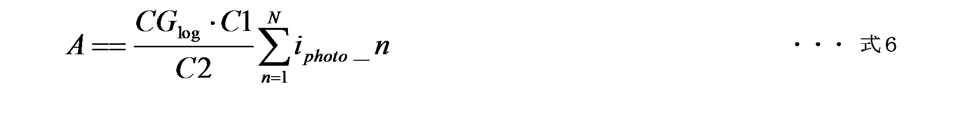
上式において、iphoto_nは、n番目の画素の光電流であり、単位は例えば、アンペア(A)である。Nは、画素ブロック310内の画素数である。
Further, assuming that the conversion gain of the current-voltage conversion unit 410 is CG log and the gain of the buffer 420 is “1”, the gain A of the entire address event detection unit 400 described above is expressed by the following equation.
In the above equation, i photo — n is the photocurrent of the nth pixel, and the unit is, for example, amperes (A). N is the number of pixels in the pixel block 310.
[カラムADCの構成例]
図9は、本技術の第1の実施の形態におけるカラムADC220の一構成例を示すブロック図である。このカラムADC220は、画素ブロック310の列ごとにADC230を備える。また、カラムADC220は、参照信号生成部231および出力部232を備える。参照信号生成部231は、ランプ信号などの参照信号を生成してADC230のそれぞれに供給するものである。参照信号生成部231として、DAC(Digital to Analog Converter)などが用いられる。出力部232は、ADC230からのデジタル信号を信号処理部212に供給するものである。 [Example of configuration of column ADC]
FIG. 9 is a block diagram showing one configuration example of thecolumn ADC 220 in the first embodiment of the present technology. The column ADC 220 includes an ADC 230 for each column of pixel blocks 310. In addition, the column ADC 220 includes a reference signal generation unit 231 and an output unit 232. The reference signal generation unit 231 generates a reference signal such as a ramp signal and supplies the reference signal to each of the ADCs 230. As the reference signal generation unit 231, a DAC (Digital to Analog Converter) or the like is used. The output unit 232 supplies the digital signal from the ADC 230 to the signal processing unit 212.
図9は、本技術の第1の実施の形態におけるカラムADC220の一構成例を示すブロック図である。このカラムADC220は、画素ブロック310の列ごとにADC230を備える。また、カラムADC220は、参照信号生成部231および出力部232を備える。参照信号生成部231は、ランプ信号などの参照信号を生成してADC230のそれぞれに供給するものである。参照信号生成部231として、DAC(Digital to Analog Converter)などが用いられる。出力部232は、ADC230からのデジタル信号を信号処理部212に供給するものである。 [Example of configuration of column ADC]
FIG. 9 is a block diagram showing one configuration example of the
ADC230は、垂直信号線VSLを介して供給されたアナログの画素信号SIGをデジタル信号に変換するものである。このADC230は、比較器231、カウンタ232、スイッチ233およびメモリ234を備える。比較器231は、参照信号と画素信号SIGとを比較し、カウンタ232は、比較結果が反転するまでの期間に亘って計数値を計数する。スイッチ233は、タイミング制御回路(不図示)などの制御に従って、計数値をメモリ234に供給して保持させる。メモリ234は、計数値を示すデジタル信号を水平駆動部(不図示)などの制御に従って出力部232に供給する。この構成により、画素信号SIGは、検出信号よりもビット数の多いデジタル信号に変換される。例えば、検出信号を2ビットとすると、画素信号は、3ビット以上(16ビットなど)のデジタル信号に変換される。なお、ADC230は、特許請求の範囲に記載のアナログデジタル変換器の一例である。
The ADC 230 converts an analog pixel signal SIG supplied via the vertical signal line VSL into a digital signal. The ADC 230 includes a comparator 231, a counter 232, a switch 233, and a memory 234. The comparator 231 compares the reference signal with the pixel signal SIG, and the counter 232 counts the count value until the comparison result is inverted. The switch 233 supplies and holds the count value to the memory 234 according to the control of the timing control circuit (not shown) or the like. The memory 234 supplies a digital signal indicating the count value to the output unit 232 according to control of a horizontal drive unit (not shown) or the like. With this configuration, the pixel signal SIG is converted to a digital signal having a larger number of bits than the detection signal. For example, assuming that the detection signal is 2 bits, the pixel signal is converted to a digital signal of 3 bits or more (16 bits or the like). The ADC 230 is an example of the analog-to-digital converter described in the claims.
[固体撮像素子の動作例]
図10は、本技術の第1の実施の形態における固体撮像素子200の動作の一例を示すタイミングチャートである。タイミングT0において、制御部130によりアドレスイベントの検出開始が指示されると、駆動回路211は、制御信号OFGnを全てハイレベルにして、全画素のOFGトランジスタ332をオン状態にする。これにより、全画素の光電流の和がアドレスイベント検出部400に供給される。一方、転送信号TRGnは全てローレベルであり、全画素の転送トランジスタ331はオフ状態である。 [Operation example of solid-state imaging device]
FIG. 10 is a timing chart showing an example of the operation of the solid-state imaging device 200 according to the first embodiment of the present technology. At timing T0, when start of detection of the address event is instructed by the control unit 130, the drive circuit 211 sets all the control signals OFGn to high level, and turns on the OFG transistors 332 of all the pixels. Thus, the sum of the photocurrents of all the pixels is supplied to the address event detection unit 400. On the other hand, all the transfer signals TRGn are at the low level, and the transfer transistors 331 of all the pixels are in the off state.
図10は、本技術の第1の実施の形態における固体撮像素子200の動作の一例を示すタイミングチャートである。タイミングT0において、制御部130によりアドレスイベントの検出開始が指示されると、駆動回路211は、制御信号OFGnを全てハイレベルにして、全画素のOFGトランジスタ332をオン状態にする。これにより、全画素の光電流の和がアドレスイベント検出部400に供給される。一方、転送信号TRGnは全てローレベルであり、全画素の転送トランジスタ331はオフ状態である。 [Operation example of solid-state imaging device]
FIG. 10 is a timing chart showing an example of the operation of the solid-
そして、タイミングT1において、アドレスイベント検出部400がアドレスイベントを検出し、ハイレベルの検出信号を出力したものとする。ここで、検出信号は、オンイベントの検出結果を示す1ビットの信号であるものとする。
Then, at timing T1, the address event detection unit 400 detects an address event and outputs a high level detection signal. Here, the detection signal is a 1-bit signal indicating the detection result of the on event.
駆動回路211は、検出信号を受け取ると、タイミングT2において制御信号OFGnを全てローレベルにしてアドレスイベント検出部400への光電流の供給を停止させる。また、駆動回路211は、選択信号SELをハイレベルにし、リセット信号RSTを一定のパルス期間に亘ってハイレベルにして浮遊拡散層324の初期化を行う。この初期化時の電圧を画素信号生成部320は、リセットレベルとして出力し、ADC230は、そのリセットレベルをデジタル信号に変換する。
When receiving the detection signal, the drive circuit 211 turns all the control signals OFGn to low level at timing T2 to stop the supply of the photocurrent to the address event detection unit 400. In addition, the drive circuit 211 causes the selection signal SEL to be high level, and causes the reset signal RST to be high level for a fixed pulse period to initialize the floating diffusion layer 324. The pixel signal generation unit 320 outputs the voltage at the time of initialization as a reset level, and the ADC 230 converts the reset level into a digital signal.
リセットレベルの変換後のタイミングT3において、駆動回路211は、一定のパルス期間に亘ってハイレベルの転送信号TRG1を供給して、1つ目の画素に電圧を信号レベルとして出力させる。ADC230は、その信号レベルをデジタル信号に変換する。信号処理部212は、リセットレベルと信号レベルとの差分を正味の画素信号として求める。この処理は、CDS処理と呼ばれる。
At timing T3 after conversion of the reset level, the drive circuit 211 supplies a high level transfer signal TRG1 for a fixed pulse period to output a voltage as a signal level to the first pixel. The ADC 230 converts the signal level into a digital signal. The signal processing unit 212 obtains a difference between the reset level and the signal level as a net pixel signal. This process is called CDS process.
信号レベルの変換後のタイミングT4において、駆動回路211は、一定のパルス期間に亘ってハイレベルの転送信号TRG2を供給して、2つ目の画素に信号レベルを出力させる。信号処理部212は、リセットレベルと信号レベルとの差分を正味の画素信号として求める。以下、同様の処理が実行されて、画素ブロック310内のそれぞれの画素の画素信号が順に出力される。
At timing T4 after signal level conversion, the drive circuit 211 supplies a high level transfer signal TRG2 for a fixed pulse period to cause the second pixel to output the signal level. The signal processing unit 212 obtains a difference between the reset level and the signal level as a net pixel signal. Thereafter, the same processing is performed, and the pixel signals of the respective pixels in the pixel block 310 are sequentially output.
全ての画素信号が出力されると、駆動回路211は、制御信号OFGnを全てハイレベルにして、全画素のOFGトランジスタ332をオン状態にする。
When all the pixel signals are output, the drive circuit 211 turns all the control signals OFGn to high level to turn on the OFG transistors 332 of all the pixels.
図11は、本技術の第1の実施の形態における固体撮像素子200の動作の一例を示すフローチャートである。この動作は、例えば、アドレスイベントを検出するための所定のアプリケーションが実行されたときに開始される。
FIG. 11 is a flowchart illustrating an example of the operation of the solid-state imaging device 200 according to the first embodiment of the present technology. This operation is started, for example, when a predetermined application for detecting an address event is executed.
画素ブロック310のそれぞれは、アドレスイベントの有無の検出を行う(ステップS901)。駆動回路211は、いずれかの画素ブロック310においてアドレスイベントがあったか否かを判断する(ステップS902)。アドレスイベントがあった場合に(ステップS902:Yes)、駆動回路211は、アドレスイベントの生じた画素ブロック310内のそれぞれの画素の画素信号を順に出力させる(ステップS903)。
Each of the pixel blocks 310 detects the presence or absence of an address event (step S901). The drive circuit 211 determines whether an address event has occurred in any of the pixel blocks 310 (step S902). When there is an address event (step S902: Yes), the drive circuit 211 sequentially outputs pixel signals of respective pixels in the pixel block 310 in which the address event has occurred (step S903).
アドレスイベントが無い場合(ステップS902:No)、または、ステップS903の後に固体撮像素子200は、ステップS901以降を繰り返す。
If there is no address event (step S902: No), or after step S903, the solid-state imaging device 200 repeats step S901 and subsequent steps.
このように、本技術の第1の実施の形態によれば、複数(N個)の光電変換素子333(画素)のそれぞれの光電流の変化量をアドレスイベント検出部400が検出するため、アドレスイベント検出部400の配置数を、N画素ごとに1つにすることができる。このようにN画素で1つのアドレスイベント検出部400を共有することにより、アドレスイベント検出部400を共有せずに画素毎に設ける構成と比較して回路規模を削減することができる。
Thus, according to the first embodiment of the present technology, the address event detection unit 400 detects the amount of change in the photocurrent of each of the (N) photoelectric conversion elements 333 (pixels). The arrangement number of event detection units 400 can be one for every N pixels. By sharing one address event detection unit 400 with N pixels in this manner, the circuit scale can be reduced as compared with the configuration provided for each pixel without sharing the address event detection unit 400.
[第1の変形例]
上述の第1の実施の形態では、光電変換素子333以外の素子を検出チップ202に配置していたが、この構成では、画素数の増大に伴って検出チップ202の回路規模が増大するおそれがある。この第1の実施の形態の第1の変形例における固体撮像素子200は、検出チップ202の回路規模を削減した点において第1の実施の形態と異なる。 [First Modification]
In the first embodiment described above, elements other than thephotoelectric conversion element 333 are disposed in the detection chip 202. However, in this configuration, the circuit scale of the detection chip 202 may increase as the number of pixels increases. is there. The solid-state imaging device 200 according to the first modification of the first embodiment is different from the first embodiment in that the circuit size of the detection chip 202 is reduced.
上述の第1の実施の形態では、光電変換素子333以外の素子を検出チップ202に配置していたが、この構成では、画素数の増大に伴って検出チップ202の回路規模が増大するおそれがある。この第1の実施の形態の第1の変形例における固体撮像素子200は、検出チップ202の回路規模を削減した点において第1の実施の形態と異なる。 [First Modification]
In the first embodiment described above, elements other than the
図12は、本技術の第1の実施の形態の第1の変形例における画素ブロック310の一構成例を示す回路図である。この第1の実施の形態の第1の変形例の画素ブロック310は、リセットトランジスタ321および浮遊拡散層324と複数の受光部330とが受光チップ201に配置される点において第1の実施の形態と異なる。これら以外の素子は、検出チップ202に配置される。
FIG. 12 is a circuit diagram showing a configuration example of the pixel block 310 in the first modified example of the first embodiment of the present technology. The pixel block 310 according to the first modification of the first embodiment is different from the first embodiment in that the reset transistor 321, the floating diffusion layer 324, and the plurality of light receiving units 330 are disposed in the light receiving chip 201. It is different from Elements other than these are disposed in the detection chip 202.
このように、本技術の第1の実施の形態の第1の変形例によれば、リセットトランジスタ321等と複数の受光部330とを受光チップ201に配置したため、第1の実施の形態と比較して検出チップ202の回路規模を削減することができる。
As described above, according to the first modification of the first embodiment of the present technology, since the reset transistor 321 and the like and the plurality of light receiving units 330 are disposed in the light receiving chip 201, comparison with the first embodiment is made. Thus, the circuit size of the detection chip 202 can be reduced.
[第2の変形例]
上述の第1の実施の形態の第1の変形例では、リセットトランジスタ321等と複数の受光部330とを受光チップ201に配置していたが、画素数の増大に伴って検出チップ202の回路規模が増大するおそれがある。この第1の実施の形態の第2の変形例における固体撮像素子200は、検出チップ202の回路規模をさらに削減した点において第1の実施の形態の第1の変形例と異なる。 Second Modified Example
In the first modification of the first embodiment described above, thereset transistor 321 and the like and the plurality of light receiving units 330 are disposed in the light receiving chip 201, but the circuit of the detection chip 202 is increased as the number of pixels increases. Scale may increase. The solid-state imaging device 200 according to the second modification of the first embodiment is different from the first modification of the first embodiment in that the circuit size of the detection chip 202 is further reduced.
上述の第1の実施の形態の第1の変形例では、リセットトランジスタ321等と複数の受光部330とを受光チップ201に配置していたが、画素数の増大に伴って検出チップ202の回路規模が増大するおそれがある。この第1の実施の形態の第2の変形例における固体撮像素子200は、検出チップ202の回路規模をさらに削減した点において第1の実施の形態の第1の変形例と異なる。 Second Modified Example
In the first modification of the first embodiment described above, the
図13は、本技術の第1の実施の形態の第2の変形例における画素ブロック310の一構成例を示す回路図である。この第1の実施の形態の第2の変形例の画素ブロック310は、N型トランジスタ411および413がさらに受光チップ201に配置される点において第1の実施の形態の第1の変形例と異なる。このように、受光チップ201内のトランジスタをN型のみにすることにより、N型トランジスタおよびP型トランジスタを混在させる場合と比較して、トランジスタを形成する際の工程数を削減することができる。これにより、受光チップ201の製造コストを削減することができる。
FIG. 13 is a circuit diagram showing a configuration example of a pixel block 310 in a second modified example of the first embodiment of the present technology. The pixel block 310 of the second modification of the first embodiment differs from the first modification of the first embodiment in that N- type transistors 411 and 413 are further arranged in the light receiving chip 201. . As described above, by making the transistors in the light receiving chip 201 only N-type, the number of processes in forming the transistors can be reduced as compared with the case where N-type transistors and P-type transistors are mixed. Thereby, the manufacturing cost of the light receiving chip 201 can be reduced.
このように、本技術の第1の実施の形態の第2の変形例によれば、N型トランジスタ411および413をさらに受光チップ201に配置したため、第1の実施の形態の第1の変形例と比較して検出チップ202の回路規模を削減することができる。
As described above, according to the second modification of the first embodiment of the present technology, since the N- type transistors 411 and 413 are further arranged in the light receiving chip 201, the first modification of the first embodiment The circuit scale of the detection chip 202 can be reduced compared to the case of FIG.
[第3の変形例]
上述の第1の実施の形態の第2の変形例では、N型トランジスタ411および413をさらに受光チップ201に配置していたが、画素数の増大に伴って検出チップ202の回路規模が増大するおそれがある。この第1の実施の形態の第3の変形例における固体撮像素子200は、検出チップ202の回路規模をさらに削減した点において第1の実施の形態の第2の変形例と異なる。 Third Modified Example
In the second modification of the first embodiment described above, the N- type transistors 411 and 413 are further arranged in the light receiving chip 201, but the circuit scale of the detection chip 202 increases with the increase in the number of pixels. There is a fear. The solid-state imaging device 200 according to the third modification of the first embodiment is different from the second modification of the first embodiment in that the circuit size of the detection chip 202 is further reduced.
上述の第1の実施の形態の第2の変形例では、N型トランジスタ411および413をさらに受光チップ201に配置していたが、画素数の増大に伴って検出チップ202の回路規模が増大するおそれがある。この第1の実施の形態の第3の変形例における固体撮像素子200は、検出チップ202の回路規模をさらに削減した点において第1の実施の形態の第2の変形例と異なる。 Third Modified Example
In the second modification of the first embodiment described above, the N-
図14は、本技術の第1の実施の形態の第3の変形例における画素ブロック310の一構成例を示す回路図である。この第1の実施の形態の第3の変形例の画素ブロック310は、増幅トランジスタ322および選択トランジスタ323がさらに受光チップ201に配置される点において第1の実施の形態の第2の変形例と異なる。すなわち、画素信号生成部320全体が受光チップ201に配置される。
FIG. 14 is a circuit diagram showing a configuration example of the pixel block 310 in the third modified example of the first embodiment of the present technology. The pixel block 310 of the third modification of the first embodiment is different from the second modification of the first embodiment in that the amplification transistor 322 and the selection transistor 323 are further disposed in the light receiving chip 201. It is different. That is, the entire pixel signal generation unit 320 is disposed in the light receiving chip 201.
このように、本技術の第1の実施の形態の第3の変形例によれば、画素信号生成部320を受光チップ201に配置したため、第1の実施の形態の第2の変形例と比較して検出チップ202の回路規模を削減することができる。
As described above, according to the third modification of the first embodiment of the present technology, since the pixel signal generation unit 320 is disposed in the light receiving chip 201, comparison with the second modification of the first embodiment is made. Thus, the circuit size of the detection chip 202 can be reduced.
<2.第2の実施の形態>
上述の第1の実施の形態では、画素ブロック310ごとに画素信号生成部320を設けていたが、画素数の増大に伴って固体撮像素子200の回路規模が増大するおそれがある。この第2の実施の形態における固体撮像素子200は、画素信号生成部320を削減した点において第1の実施の形態と異なる。 <2. Second embodiment>
Although the pixelsignal generation unit 320 is provided for each pixel block 310 in the first embodiment described above, the circuit scale of the solid-state imaging device 200 may increase as the number of pixels increases. The solid-state imaging device 200 according to the second embodiment is different from the first embodiment in that the pixel signal generation unit 320 is eliminated.
上述の第1の実施の形態では、画素ブロック310ごとに画素信号生成部320を設けていたが、画素数の増大に伴って固体撮像素子200の回路規模が増大するおそれがある。この第2の実施の形態における固体撮像素子200は、画素信号生成部320を削減した点において第1の実施の形態と異なる。 <2. Second embodiment>
Although the pixel
図15は、本技術の第2の実施の形態における画素アレイ部300の一構成例を示すブロック図である。この画素アレイ部300は、画素信号生成部320が設けられていない点において第1の実施の形態と異なる。
FIG. 15 is a block diagram showing a configuration example of the pixel array unit 300 according to the second embodiment of the present technology. The pixel array unit 300 is different from the first embodiment in that the pixel signal generation unit 320 is not provided.
また、第2の実施の形態のアドレスイベント検出部400は、画素信号SIGを生成し、垂直信号線VSLを介して出力する点において第1の実施の形態と異なる。
Further, the address event detection unit 400 of the second embodiment is different from the first embodiment in that the pixel signal SIG is generated and output via the vertical signal line VSL.
図16は、本技術の第2の実施の形態における受光部330の一構成例を示す回路図である。この第2の実施の形態の受光部330は、OFGトランジスタ332を備えない点において第1の実施の形態と異なる。
FIG. 16 is a circuit diagram showing one configuration example of the light receiving unit 330 in the second embodiment of the present technology. The light receiving unit 330 of the second embodiment differs from the first embodiment in that the OFG transistor 332 is not provided.
また、第2の実施の形態の転送トランジスタ331は、光電変換素子333からの光電流を接続ノード340を介してアドレスイベント検出部400に供給する。
In addition, the transfer transistor 331 of the second embodiment supplies the photocurrent from the photoelectric conversion element 333 to the address event detection unit 400 via the connection node 340.
なお、受光部330のそれぞれに転送トランジスタ331を配置しているが、図17に例示するように、これらのトランジスタを設けない構成とすることもできる。この場合には駆動回路211は、受光部330へ転送信号TRGnを供給する必要が無くなる。
Although the transfer transistor 331 is disposed in each of the light receiving sections 330, as shown in FIG. 17, these transistors may not be provided. In this case, the drive circuit 211 need not supply the transfer signal TRGn to the light receiving unit 330.
図18は、本技術の第2の実施の形態における電流電圧変換部410の一構成例を示す回路図である。この第2の実施の形態の電流電圧変換部410は、N型トランジスタ413のソースが垂直信号線VSLに接続される点において第1の実施の形態と異なる。
FIG. 18 is a circuit diagram showing a configuration example of the current-voltage conversion unit 410 in the second embodiment of the present technology. The current-voltage conversion unit 410 of the second embodiment is different from that of the first embodiment in that the source of the N-type transistor 413 is connected to the vertical signal line VSL.
また、駆動回路211は、アドレスイベントが検出されると、P型トランジスタ412のゲートへの電圧(Vbias)を検出前よりも低下させてローレベルにする。これにより、N型トランジスタ411のゲートの電圧は、ドレインと同様に電源電圧VDDとなり、N型トランジスタ411はダイオード接続された場合と等価な状態となる。そして、ソースフォロワとして機能するN型トランジスタ413により、光電流に応じた電圧の画素信号SIGが生成される。
In addition, when an address event is detected, the drive circuit 211 lowers the voltage (V bias ) to the gate of the P-type transistor 412 to a low level as compared to before the detection. As a result, the voltage at the gate of the N-type transistor 411 becomes the power supply voltage VDD as in the case of the drain, and the N-type transistor 411 is in a state equivalent to a diode connection. Then, the pixel signal SIG of a voltage corresponding to the photocurrent is generated by the N-type transistor 413 functioning as a source follower.
また、複数の受光部330と、N型トランジスタ411および413は、受光チップ201に配置され、残りの素子は、検出チップ202に配置される。
Further, the plurality of light receiving units 330 and the N- type transistors 411 and 413 are disposed in the light receiving chip 201, and the remaining elements are disposed in the detection chip 202.
図19は、本技術の第2の実施の形態における固体撮像素子200の動作の一例を示すタイミングチャートである。
FIG. 19 is a timing chart showing an example of the operation of the solid-state imaging device 200 according to the second embodiment of the present technology.
タイミングT0において、アドレスイベントの検出開始が指示されると、駆動回路211は、転送信号TRGnを全てハイレベルにして、全画素の転送トランジスタ331をオン状態にする。
At timing T0, when the start of detection of the address event is instructed, the drive circuit 211 sets all the transfer signals TRGn to high level, and turns on the transfer transistors 331 of all the pixels.
そして、タイミングT1において、アドレスイベント検出部400がアドレスイベントを検出し、ハイレベルの検出信号を出力したものとする。
Then, at timing T1, the address event detection unit 400 detects an address event and outputs a high level detection signal.
駆動回路211は、検出信号を受け取ると、タイミングT2において一定のパルス期間に亘って、転送信号TRG1のみをハイレベルにする。画素信号生成部320は、1つ目の画素の画素信号をデジタル信号に変換する。
When receiving the detection signal, the drive circuit 211 sets only the transfer signal TRG1 to a high level for a certain pulse period at timing T2. The pixel signal generation unit 320 converts the pixel signal of the first pixel into a digital signal.
画素信号の変換後のタイミングT3において、駆動回路211は、一定のパルス期間に亘ってハイレベルの転送信号TRG2をハイレベルにする。画素信号生成部320は、2つ目の画素の画素信号をデジタル信号に変換する。以下、同様の処理が実行されて、画素ブロック310内のそれぞれの画素の画素信号が順に出力される。
At timing T3 after the conversion of the pixel signal, the drive circuit 211 sets the high level transfer signal TRG2 to the high level for a certain pulse period. The pixel signal generation unit 320 converts the pixel signal of the second pixel into a digital signal. Thereafter, the same processing is performed, and the pixel signals of the respective pixels in the pixel block 310 are sequentially output.
全ての画素信号が出力されると、駆動回路211は、転送信号TRGnを全てハイレベルにして、全画素の転送トランジスタ331をオン状態にする。
When all the pixel signals are output, the drive circuit 211 turns all the transfer signals TRGn to high level, and turns on the transfer transistors 331 of all the pixels.
このように、本技術の第2の実施の形態では、アドレスイベント検出部400が画素信号SIGを生成するため、画素信号生成部320を配置する必要が無くなる。これにより、画素信号生成部320を配置する第1の実施の形態と比較して回路規模を削減することができる。
As described above, in the second embodiment of the present technology, since the address event detection unit 400 generates the pixel signal SIG, it is not necessary to arrange the pixel signal generation unit 320. Thus, the circuit scale can be reduced as compared to the first embodiment in which the pixel signal generation unit 320 is disposed.
[変形例]
上述の第2の実施の形態では、ADC230全体を検出チップ202に配置していたが、画素数の増大に伴って検出チップ202の回路規模が増大するおそれがある。この第2の実施の形態の変形例における固体撮像素子200は、ADC230の一部を受光チップ201に配置して検出チップ202の回路規模を削減した点において第2の実施の形態と異なる。 [Modification]
Although theentire ADC 230 is disposed in the detection chip 202 in the second embodiment described above, the circuit scale of the detection chip 202 may increase as the number of pixels increases. The solid-state imaging device 200 according to the modification of the second embodiment differs from the second embodiment in that a part of the ADC 230 is disposed on the light receiving chip 201 to reduce the circuit size of the detection chip 202.
上述の第2の実施の形態では、ADC230全体を検出チップ202に配置していたが、画素数の増大に伴って検出チップ202の回路規模が増大するおそれがある。この第2の実施の形態の変形例における固体撮像素子200は、ADC230の一部を受光チップ201に配置して検出チップ202の回路規模を削減した点において第2の実施の形態と異なる。 [Modification]
Although the
図20は、本技術の第2の実施の形態の変形例における電流電圧変換部410の一構成例を示す回路図である。この第2の実施の形態の変形例の電流電圧変換部410は、N型トランジスタ413のソースは接地され、N型トランジスタ411のドレインが垂直信号線VSLに接続されている点において第2の実施の形態と異なる。なお、第2の実施の形態と同様に、N型トランジスタ411の代わりに、N型トランジスタ413のソースを垂直信号線VSLに接続することもできる。
FIG. 20 is a circuit diagram showing a configuration example of a current-voltage conversion unit 410 in a modification of the second embodiment of the present technology. The current-voltage conversion unit 410 according to the modification of the second embodiment is a second embodiment in that the source of the N-type transistor 413 is grounded and the drain of the N-type transistor 411 is connected to the vertical signal line VSL. It differs from the form of As in the second embodiment, instead of the N-type transistor 411, the source of the N-type transistor 413 can be connected to the vertical signal line VSL.
図21は、本技術の第2の実施の形態の変形例におけるADC230の一構成例を示す回路図である。このADC230は、差動増幅回路240およびカウンタ250を備える。
FIG. 21 is a circuit diagram showing a configuration example of an ADC 230 in a modification of the second embodiment of the present technology. The ADC 230 includes a differential amplifier circuit 240 and a counter 250.
差動増幅回路240は、N型トランジスタ243、244および245と、P型トランジスタ241および242とを備える。これらのトランジスタとして、例えば、MOSトランジスタが用いられる。
Differential amplifier circuit 240 includes N- type transistors 243, 244 and 245 and P- type transistors 241 and 242. As these transistors, for example, MOS transistors are used.
N型トランジスタ243および244は、差動対を構成し、これらのトランジスタのソースは、N型トランジスタ245のドレインに共通に接続される。また、N型トランジスタ243のドレインは、P型トランジスタ241のドレインとP型トランジスタ241および242のゲートとに接続される。N型トランジスタ244のドレインは、P型トランジスタ242のドレインとカウンタ250とに接続される。また、N型トランジスタ243のゲートには、参照信号REFが入力され、N型トランジスタ244のゲートには、垂直信号線VSLを介して画素信号SIGが入力される。なお、N型トランジスタ243は、特許請求の範囲に記載の参照側トランジスタの一例であり、N型トランジスタ244は、特許請求の範囲に記載の信号側トランジスタの一例である。
N- type transistors 243 and 244 form a differential pair, and the sources of these transistors are commonly connected to the drain of N-type transistor 245. The drain of the N-type transistor 243 is connected to the drain of the P-type transistor 241 and the gates of the P- type transistors 241 and 242. The drain of the N-type transistor 244 is connected to the drain of the P-type transistor 242 and the counter 250. Further, the reference signal REF is input to the gate of the N-type transistor 243, and the pixel signal SIG is input to the gate of the N-type transistor 244 via the vertical signal line VSL. The N-type transistor 243 is an example of the reference-side transistor described in the claims, and the N-type transistor 244 is an example of the signal-side transistor described in the claims.
参照信号REFとして、例えば、ランプ信号が用いられる。参照信号REFを生成する回路は、省略されている。
For example, a ramp signal is used as the reference signal REF. The circuit that generates the reference signal REF is omitted.
N型トランジスタ245のゲートには、所定のバイアス電圧Vbが印加され、そのソースは接地される。このN型トランジスタ245は、一定の電流を供給する。なお、N型トランジスタ245は、特許請求の範囲に記載の定電流源の一例である。
A predetermined bias voltage Vb is applied to the gate of the N-type transistor 245, and the source is grounded. The N-type transistor 245 supplies a constant current. The N-type transistor 245 is an example of a constant current source described in the claims.
上述の構成により、P型トランジスタ241および242は、カレントミラー回路を構成し、参照信号REFと画素信号SIGとの差を増幅してカウンタ250に出力する。そして、カウンタ250は、差動増幅回路240からの信号が反転するまでの期間に亘って計数値を計数し、計数値を示すデジタル信号を信号処理部212に出力する。
With the configuration described above, P- type transistors 241 and 242 form a current mirror circuit, which amplifies the difference between reference signal REF and pixel signal SIG and outputs the result to counter 250. Then, the counter 250 counts the count value during a period until the signal from the differential amplifier circuit 240 is inverted, and outputs a digital signal indicating the count value to the signal processing unit 212.
また、上述の第2の実施の形態の変形例において、受光チップ201には、上述のN型トランジスタ243、244および245がさらに設けられる。
Further, in the modification of the second embodiment described above, the light receiving chip 201 is further provided with the N- type transistors 243, 244 and 245 described above.
このように、本技術の第2の実施の形態の変形例によれば、N型トランジスタ243、244および245をさらに受光チップ201に配置したため、第2の実施の形態と比較して検出チップ202の回路規模を削減することができる。
As described above, according to the modification of the second embodiment of the present technology, since the N- type transistors 243, 244 and 245 are further disposed in the light receiving chip 201, the detection chip 202 is compared with the second embodiment. Circuit size can be reduced.
<3.第3の実施の形態>
上述の第2の実施の形態では、コンデンサ431および433をアドレスイベント検出部400内に配置していたが、式5より容量C1を削減すると利得が悪化するため、容量C1の削減により回路の動作速度を向上させることは困難である。この第3の実施の形態における固体撮像素子200は、画素毎にコンデンサ431を配置して、動作速度を向上させた点において第2の実施の形態と異なる。 <3. Third embodiment>
In the second embodiment described above, the capacitors 431 and 433 are disposed in the address event detection unit 400. However, if the capacitance C1 is reduced according to Equation 5, the gain is degraded. It is difficult to improve the speed. The solid-state imaging device 200 according to the third embodiment is different from that according to the second embodiment in that the capacitor 431 is provided for each pixel to improve the operation speed.
上述の第2の実施の形態では、コンデンサ431および433をアドレスイベント検出部400内に配置していたが、式5より容量C1を削減すると利得が悪化するため、容量C1の削減により回路の動作速度を向上させることは困難である。この第3の実施の形態における固体撮像素子200は、画素毎にコンデンサ431を配置して、動作速度を向上させた点において第2の実施の形態と異なる。 <3. Third embodiment>
In the second embodiment described above, the
図22は、本技術の第3の実施の形態における画素アレイ部300の一構成例を示すブロック図である。この第3の実施の形態の画素アレイ部300は、アドレスイベント検出部400の代わりに受光部330のそれぞれが画素信号SIGを生成する点において第2の実施の形態と異なる。また、垂直信号線VSLは、例えば、画素の列ごとに配線される。そして、ADC230も、画素の列ごとに設けられる。なお、第2の実施の形態と同様に垂直信号線VSLを画素ブロック310の列ごとに配置し、受光部330のそれぞれを接続することもできる。この場合には、ADC230も画素ブロック310の列ごとに設けられる。
FIG. 22 is a block diagram showing a configuration example of the pixel array unit 300 according to the third embodiment of the present technology. The pixel array unit 300 according to the third embodiment is different from that according to the second embodiment in that each of the light receiving units 330 generates a pixel signal SIG instead of the address event detecting unit 400. Also, the vertical signal line VSL is wired, for example, for each column of pixels. The ADC 230 is also provided for each column of pixels. As in the second embodiment, the vertical signal lines VSL may be disposed for each column of the pixel blocks 310, and the light receiving units 330 may be connected to each other. In this case, the ADC 230 is also provided for each column of the pixel block 310.
図23は、本技術の第3の実施の形態における受光部330の一構成例を示す回路図である。この第3の実施の形態の受光部330は、電流電圧変換部410、バッファ420およびコンデンサ431をさらに備える点において第2の実施の形態と異なる。
FIG. 23 is a circuit diagram showing a configuration example of the light receiving unit 330 in the third embodiment of the present technology. The light receiving unit 330 according to the third embodiment is different from that according to the second embodiment in that the current / voltage converting unit 410, the buffer 420, and the capacitor 431 are further provided.
第3の実施の形態の電流電圧変換部410の回路構成は、例えば、図19に例示した第2の実施の形態の変形例と同様である。また、第3の実施の形態における駆動回路211の動作は、第2の実施の形態と同様である。また、第3の実施の形態において受光チップ201および検出チップ202のそれぞれに配置される回路や素子は、第2の実施の形態の変形例と同様である。すなわち、図20に例示したように、電流電圧変換部410においてN型トランジスタ411および413が受光チップ201に配置される。また、図21に例示したように、ADC230において、N型トランジスタ243、244および245が受光チップ201に配置される。
The circuit configuration of the current-voltage conversion unit 410 of the third embodiment is, for example, the same as that of the modification of the second embodiment illustrated in FIG. Further, the operation of the drive circuit 211 in the third embodiment is the same as that in the second embodiment. Further, circuits and elements disposed in each of the light receiving chip 201 and the detection chip 202 in the third embodiment are the same as those of the modification of the second embodiment. That is, as illustrated in FIG. 20, the N- type transistors 411 and 413 are disposed in the light receiving chip 201 in the current voltage conversion unit 410. Further, as illustrated in FIG. 21, in the ADC 230, N- type transistors 243, 244 and 245 are disposed in the light receiving chip 201.
図24は、本技術の第3の実施の形態におけるアドレスイベント検出部400の一構成例を示すブロック図である。この第3の実施の形態のアドレスイベント検出部400は、電流電圧変換部410、バッファ420およびコンデンサ431が設けられない点において第2の実施の形態と異なる。
FIG. 24 is a block diagram showing a configuration example of the address event detection unit 400 according to the third embodiment of the present technology. The address event detection unit 400 according to the third embodiment is different from the second embodiment in that the current-voltage conversion unit 410, the buffer 420, and the capacitor 431 are not provided.
上述したように、第3の実施の形態では、並列接続された複数の受光部330が1つのコンデンサ431を共有していた第2の実施の形態と異なり、受光部330ごとにコンデンサ431が設けられる。このため、コンデンサ431の個々の容量は、受光部330の個数(すなわち、画素数)をNとすると、(C1)/Nでよい。この容量の削減により回路の動作速度を向上させることができる。ただし、第3の実施の形態の全体のゲインAは、次の式により表される。
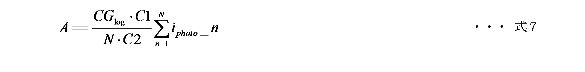
As described above, in the third embodiment, unlike the second embodiment in which the plurality of light receiving units 330 connected in parallel share one capacitor 431, the capacitor 431 is provided for each light receiving unit 330. Be Therefore, the individual capacitance of the capacitor 431 may be (C1) / N, where N is the number of light receiving portions 330 (ie, the number of pixels). The reduction of the capacity can improve the operating speed of the circuit. However, the overall gain A of the third embodiment is expressed by the following equation.
式6および式7より、第3の実施の形態のゲインAは、第1および第2の実施の形態よりも小さくなる。このため、動作速度の向上の代わりに、アドレスイベントの検出精度が低下してしまう。
From Equations 6 and 7, the gain A of the third embodiment is smaller than that of the first and second embodiments. For this reason, the detection accuracy of the address event is reduced instead of the improvement of the operation speed.
このように、本技術の第3の実施の形態によれば、コンデンサ431を受光部330ごとに配置したため、複数の受光部330がコンデンサ431を共有する場合と比較して、コンデンサ431を含む回路の動作速度を向上させることができる。
As described above, according to the third embodiment of the present technology, since the capacitor 431 is disposed for each light receiving unit 330, a circuit including the capacitor 431 compared to the case where the plurality of light receiving units 330 share the capacitor 431. Operation speed can be improved.
[変形例]
上述の第3の実施の形態では、列内の複数の受光部330(画素)が1つのADC230を共有していたが、それらの画素の画素信号を順にデジタル信号に変換する必要があるため、列内の画素数が多くなるほど、画素信号の読出し速度が低下してしまう。この第3の実施の形態の変形例における固体撮像素子200は、画素ごとにADC230を配置した点において第3の実施の形態と異なる。 [Modification]
In the third embodiment described above, although the plurality of light receiving units 330 (pixels) in a column share oneADC 230, it is necessary to sequentially convert the pixel signals of those pixels into digital signals. As the number of pixels in a column increases, the readout speed of the pixel signal decreases. The solid-state imaging device 200 according to the modification of the third embodiment differs from the third embodiment in that the ADC 230 is disposed for each pixel.
上述の第3の実施の形態では、列内の複数の受光部330(画素)が1つのADC230を共有していたが、それらの画素の画素信号を順にデジタル信号に変換する必要があるため、列内の画素数が多くなるほど、画素信号の読出し速度が低下してしまう。この第3の実施の形態の変形例における固体撮像素子200は、画素ごとにADC230を配置した点において第3の実施の形態と異なる。 [Modification]
In the third embodiment described above, although the plurality of light receiving units 330 (pixels) in a column share one
図25は、本技術の第3の実施の形態の変形例における受光部330の一構成例を示す回路図である。この第3の実施の形態の変形例の受光部330は、ADC230をさらに備える点において第3の実施の形態と異なる。
FIG. 25 is a circuit diagram showing a configuration example of a light receiving unit 330 in a modification of the third embodiment of the present technology. The light receiving unit 330 of the modification of the third embodiment is different from that of the third embodiment in that the light receiving unit 330 further includes an ADC 230.
このように、本技術の第3の実施の形態の変形例によれば、受光部330ごとにADC230を配置したため、複数の受光部330が1つのADC230を共有する構成と比較して画素信号の読出し速度を向上させることができる。
As described above, according to the modification of the third embodiment of the present technology, since the ADC 230 is disposed for each light receiving unit 330, compared to a configuration in which a plurality of light receiving units 330 share one ADC 230, The reading speed can be improved.
<4.第4の実施の形態>
上述の第1の実施の形態では、複数の画素からなる画素ブロック310ごとにアドレスイベントを検出していたが、個々の画素で生じたアドレスイベントを検出することはできない。この第4の実施の形態の固体撮像素子200は、画素毎にアドレスイベント検出部400を配置した点において第1の実施の形態と異なる。 <4. Fourth embodiment>
In the first embodiment described above, although the address event is detected for each pixel block 310 composed of a plurality of pixels, it is not possible to detect the address event generated in each pixel. The solid-state imaging device 200 according to the fourth embodiment is different from that according to the first embodiment in that an address event detection unit 400 is disposed for each pixel.
上述の第1の実施の形態では、複数の画素からなる画素ブロック310ごとにアドレスイベントを検出していたが、個々の画素で生じたアドレスイベントを検出することはできない。この第4の実施の形態の固体撮像素子200は、画素毎にアドレスイベント検出部400を配置した点において第1の実施の形態と異なる。 <4. Fourth embodiment>
In the first embodiment described above, although the address event is detected for each pixel block 310 composed of a plurality of pixels, it is not possible to detect the address event generated in each pixel. The solid-
図26は、本技術の第4の実施の形態における画素アレイ部300の一構成例を示すブロック図である。この第4の実施の形態の画素アレイ部300は、複数の画素311が二次元格子状に配列される点において第1の実施の形態と異なる。画素311のそれぞれには、画素信号生成部320、受光部330およびアドレスイベント検出部400が配置される。画素信号生成部320、受光部330およびアドレスイベント検出部400のそれぞれの回路構成は、第1の実施の形態と同様である。
FIG. 26 is a block diagram showing a configuration example of the pixel array unit 300 according to the fourth embodiment of the present technology. The pixel array unit 300 of the fourth embodiment is different from the first embodiment in that a plurality of pixels 311 are arranged in a two-dimensional grid. In each of the pixels 311, a pixel signal generating unit 320, a light receiving unit 330, and an address event detecting unit 400 are disposed. The circuit configuration of each of the pixel signal generation unit 320, the light reception unit 330, and the address event detection unit 400 is the same as that of the first embodiment.
また、受光チップ201および検出チップ202のそれぞれに配置される回路や素子は、第1の実施の形態と、第1の実施の形態の第1、第2および第3の変形例とのいずれかと同様である。例えば、図5に例示したように、光電変換素子333のみが受光チップ201に配置され、残りが検出チップ202に配置される。
In addition, the circuits and elements disposed in each of the light receiving chip 201 and the detection chip 202 are the same as those of the first embodiment and any of the first, second, and third modified examples of the first embodiment. It is similar. For example, as illustrated in FIG. 5, only the photoelectric conversion element 333 is disposed in the light receiving chip 201, and the rest is disposed in the detection chip 202.
このように、本技術の第4の実施の形態によれば、画素毎にアドレスイベント検出部400を配置したため、画素毎にアドレスイベントを検出することができる。これにより、画素ブロック310ごとにアドレスイベントを検出する場合と比較して、アドレスイベントの検出データの解像度を向上させることができる。
As described above, according to the fourth embodiment of the present technology, since the address event detection unit 400 is arranged for each pixel, an address event can be detected for each pixel. Thereby, the resolution of the detection data of the address event can be improved as compared to the case where the address event is detected for each pixel block 310.
[変形例]
上述の第4の実施の形態では、全ての画素にアドレスイベント検出部400を配置していたが、画素数の増大に伴って固体撮像素子200の回路規模が増大するおそれがある。この第4の実施の形態の変形例における固体撮像素子200は、複数の画素のうち検出対象の画素にのみアドレスイベント検出部400を配置する点において第4の実施の形態と異なる。 [Modification]
In the fourth embodiment described above, the addressevent detection unit 400 is disposed in all the pixels, but the circuit scale of the solid-state imaging device 200 may increase as the number of pixels increases. The solid-state imaging device 200 according to the modification of the fourth embodiment is different from the fourth embodiment in that the address event detection unit 400 is disposed only in the pixel to be detected among the plurality of pixels.
上述の第4の実施の形態では、全ての画素にアドレスイベント検出部400を配置していたが、画素数の増大に伴って固体撮像素子200の回路規模が増大するおそれがある。この第4の実施の形態の変形例における固体撮像素子200は、複数の画素のうち検出対象の画素にのみアドレスイベント検出部400を配置する点において第4の実施の形態と異なる。 [Modification]
In the fourth embodiment described above, the address
図27は、本技術の第4の実施の形態の変形例における画素アレイ部300の一構成例を示すブロック図である。この第4の実施の形態の変形例の画素アレイ部300は、アドレスイベント検出部400が配置されない画素と、アドレスイベント検出部400が配置される画素とが配列される点において第4の実施の形態と異なる。前者を通常画素312とし、後者をアドレスイベント検出画素313とする。アドレスイベント検出画素313は、例えば、一定間隔で互いに離隔して配置される。なお、複数のアドレスイベント検出画素313を隣接して配置することもできる。
FIG. 27 is a block diagram showing a configuration example of the pixel array unit 300 in the modification of the fourth embodiment of the present technology. The pixel array unit 300 according to the modification of the fourth embodiment is different from the pixel array according to the fourth embodiment in that pixels where the address event detection unit 400 is not disposed and pixels where the address event detection unit 400 is disposed are arranged. It is different from the form. The former is a normal pixel 312, and the latter is an address event detection pixel 313. The address event detection pixels 313 are spaced apart from each other at regular intervals, for example. A plurality of address event detection pixels 313 can be arranged adjacent to each other.
また、アドレスイベント検出画素313の構成は、第4の実施の形態の画素311と同様である。通常画素312の詳細については後述する。
In addition, the configuration of the address event detection pixel 313 is the same as that of the pixel 311 in the fourth embodiment. Details of the normal pixels 312 will be described later.
図28は、本技術の第4の実施の形態の変形例における通常画素312の一構成例を示す回路図である。この第4の実施の形態の変形例の通常画素312は、光電変換素子333、転送トランジスタ331、リセットトランジスタ321、増幅トランジスタ322、選択トランジスタ323および浮遊拡散層324を備える。これらの素子の接続構成は、図5に例示した第1の実施の形態と同様である。
FIG. 28 is a circuit diagram showing a configuration example of the normal pixel 312 in a modification of the fourth embodiment of the present technology. The normal pixel 312 according to the modification of the fourth embodiment includes a photoelectric conversion element 333, a transfer transistor 331, a reset transistor 321, an amplification transistor 322, a selection transistor 323, and a floating diffusion layer 324. The connection configuration of these elements is the same as that of the first embodiment illustrated in FIG.
このように、本技術の第4の実施の形態の変形例によれば、全画素のうちアドレスイベント検出画素313のみにアドレスイベント検出部400を配置したため、全画素にアドレスイベント検出部400を配置する構成と比較して回路規模を削減することができる。
Thus, according to the modification of the fourth embodiment of the present technology, since the address event detection unit 400 is arranged only in the address event detection pixel 313 among all pixels, the address event detection unit 400 is arranged in all pixels. The circuit scale can be reduced as compared with the configuration described above.
<5.第5の実施の形態>
上述の第1の実施の形態では、アドレスイベント検出部400を共有する画素数と画像信号生成部320を共有する画素数とを同一にしていたが、後者の方を少なくすることもできる。この第5の実施の形態の固体撮像素子200は、画像信号生成部320を共有する画素数が、アドレスイベント検出部400を共有する画素数よりも少ない点において第1の実施の形態と異なる。 <5. Fifth embodiment>
In the first embodiment described above, the number of pixels sharing the addressevent detection unit 400 and the number of pixels sharing the image signal generation unit 320 are the same, but the latter can be reduced. The solid-state imaging device 200 according to the fifth embodiment is different from the first embodiment in that the number of pixels sharing the image signal generation unit 320 is smaller than the number of pixels sharing the address event detection unit 400.
上述の第1の実施の形態では、アドレスイベント検出部400を共有する画素数と画像信号生成部320を共有する画素数とを同一にしていたが、後者の方を少なくすることもできる。この第5の実施の形態の固体撮像素子200は、画像信号生成部320を共有する画素数が、アドレスイベント検出部400を共有する画素数よりも少ない点において第1の実施の形態と異なる。 <5. Fifth embodiment>
In the first embodiment described above, the number of pixels sharing the address
図29は、本技術の第5の実施の形態における画素アレイ部300の一構成例を示すブロック図である。この第5の実施の形態の画素アレイ部300において、画素ブロック310のそれぞれには、N個の受光部330(画素)と、1つのアドレスイベント検出部400が配置される。また、画素ブロック310のそれぞれにおいて、M(Mは、N未満の整数)個の受光部330(画素)ごとに画素信号生成部320が配置される。
FIG. 29 is a block diagram illustrating a configuration example of the pixel array unit 300 according to the fifth embodiment of the present technology. In the pixel array unit 300 according to the fifth embodiment, N light receiving units 330 (pixels) and one address event detecting unit 400 are disposed in each of the pixel blocks 310. Further, in each of the pixel blocks 310, a pixel signal generation unit 320 is disposed for each of M (M is an integer less than N) light receiving units 330 (pixels).
図30は、本技術の第5の実施の形態における画素ブロック310の一構成例を示すブロック図である。画素ブロック310のそれぞれにおいて、N個の受光部330(画素)は、1つのアドレスイベント検出部400を共有する。また、M個の画素が、1つの画像信号生成部320を共有する。画像信号生成部320は、対応するM個の画素のうち選択された画素の画素信号を生成する。
FIG. 30 is a block diagram illustrating a configuration example of the pixel block 310 according to the fifth embodiment of the present technology. In each of the pixel blocks 310, the N light receiving units 330 (pixels) share one address event detecting unit 400. In addition, M pixels share one image signal generation unit 320. The image signal generation unit 320 generates a pixel signal of a pixel selected from among the corresponding M pixels.
このように、本技術の第5の実施の形態によれば、アドレスイベント検出部400を共有する画素数よりも、画像信号生成部320を共有する画素数を少なくしたため、それらを同一にする場合よりも画素信号の読出し速度を向上させることができる。
As described above, according to the fifth embodiment of the present technology, the number of pixels sharing the image signal generation unit 320 is smaller than the number of pixels sharing the address event detection unit 400. The reading speed of the pixel signal can be improved more than that.
<6.第6の実施の形態>
上述の第1の実施の形態では、画像信号生成部320およびアドレスイベント検出部400を複数の画素が共有していたが、画素毎にアドレスイベント検出部400を配置することもできる。この第6の実施の形態の固体撮像素子200は、画像信号生成部320を複数の画素が共有しつつ、画素毎にアドレスイベント検出部400を配置した点において第1の実施の形態と異なる。 <6. Sixth embodiment>
In the first embodiment described above, the imagesignal generation unit 320 and the address event detection unit 400 are shared by a plurality of pixels, but the address event detection unit 400 may be disposed for each pixel. The solid-state imaging device 200 according to the sixth embodiment is different from that according to the first embodiment in that an address event detection unit 400 is disposed for each pixel while the image signal generation unit 320 is shared by a plurality of pixels.
上述の第1の実施の形態では、画像信号生成部320およびアドレスイベント検出部400を複数の画素が共有していたが、画素毎にアドレスイベント検出部400を配置することもできる。この第6の実施の形態の固体撮像素子200は、画像信号生成部320を複数の画素が共有しつつ、画素毎にアドレスイベント検出部400を配置した点において第1の実施の形態と異なる。 <6. Sixth embodiment>
In the first embodiment described above, the image
図31は、本技術の第6の実施の形態における画素ブロック310の一構成例を示すブロック図である。画素ブロック310のそれぞれにおいて、N個の受光部330(画素)は、1つの画素信号生成部320を共有する。一方、受光部330(画素)ごとに、アドレスイベント検出部400が配置され、受光部330は、対応するアドレスイベント検出部400と接続される。
FIG. 31 is a block diagram illustrating a configuration example of the pixel block 310 according to the sixth embodiment of the present technology. In each of the pixel blocks 310, the N light receiving units 330 (pixels) share one pixel signal generating unit 320. On the other hand, an address event detection unit 400 is disposed for each light receiving unit 330 (pixel), and the light receiving unit 330 is connected to the corresponding address event detection unit 400.
このように、本技術の第6の実施の形態によれば、画素毎にアドレスイベント検出部400を配置したため、画素毎にアドレスイベントの有無を検出することができる。
As described above, according to the sixth embodiment of the present technology, since the address event detection unit 400 is arranged for each pixel, the presence or absence of the address event can be detected for each pixel.
<7.移動体への応用例>
本開示に係る技術(本技術)は、様々な製品へ応用することができる。例えば、本開示に係る技術は、自動車、電気自動車、ハイブリッド電気自動車、自動二輪車、自転車、パーソナルモビリティ、飛行機、ドローン、船舶、ロボット等のいずれかの種類の移動体に搭載される装置として実現されてもよい。 <7. Applications to mobiles>
The technology according to the present disclosure (the present technology) can be applied to various products. For example, the technology according to the present disclosure is realized as a device mounted on any type of mobile object such as a car, an electric car, a hybrid electric car, a motorcycle, a bicycle, personal mobility, an airplane, a drone, a ship, a robot May be
図32は、本開示に係る技術が適用され得る移動体制御システムの一例である車両制御システムの概略的な構成例を示すブロック図である。
FIG. 32 is a block diagram showing a schematic configuration example of a vehicle control system that is an example of a mobile control system to which the technology according to the present disclosure can be applied.
車両制御システム12000は、通信ネットワーク12001を介して接続された複数の電子制御ユニットを備える。図32に示した例では、車両制御システム12000は、駆動系制御ユニット12010、ボディ系制御ユニット12020、車外情報検出ユニット12030、車内情報検出ユニット12040、及び統合制御ユニット12050を備える。また、統合制御ユニット12050の機能構成として、マイクロコンピュータ12051、音声画像出力部12052、及び車載ネットワークI/F(interface)12053が図示されている。
Vehicle control system 12000 includes a plurality of electronic control units connected via communication network 12001. In the example shown in FIG. 32, the vehicle control system 12000 includes a drive system control unit 12010, a body system control unit 12020, an external information detection unit 12030, an in-vehicle information detection unit 12040, and an integrated control unit 12050. Further, as a functional configuration of the integrated control unit 12050, a microcomputer 12051, an audio image output unit 12052, and an in-vehicle network I / F (interface) 12053 are illustrated.
駆動系制御ユニット12010は、各種プログラムにしたがって車両の駆動系に関連する装置の動作を制御する。例えば、駆動系制御ユニット12010は、内燃機関又は駆動用モータ等の車両の駆動力を発生させるための駆動力発生装置、駆動力を車輪に伝達するための駆動力伝達機構、車両の舵角を調節するステアリング機構、及び、車両の制動力を発生させる制動装置等の制御装置として機能する。
The driveline control unit 12010 controls the operation of devices related to the driveline of the vehicle according to various programs. For example, the drive system control unit 12010 includes a drive force generation device for generating a drive force of a vehicle such as an internal combustion engine or a drive motor, a drive force transmission mechanism for transmitting the drive force to the wheels, and a steering angle of the vehicle. It functions as a control mechanism such as a steering mechanism that adjusts and a braking device that generates a braking force of the vehicle.
ボディ系制御ユニット12020は、各種プログラムにしたがって車体に装備された各種装置の動作を制御する。例えば、ボディ系制御ユニット12020は、キーレスエントリシステム、スマートキーシステム、パワーウィンドウ装置、あるいは、ヘッドランプ、バックランプ、ブレーキランプ、ウィンカー又はフォグランプ等の各種ランプの制御装置として機能する。この場合、ボディ系制御ユニット12020には、鍵を代替する携帯機から発信される電波又は各種スイッチの信号が入力され得る。ボディ系制御ユニット12020は、これらの電波又は信号の入力を受け付け、車両のドアロック装置、パワーウィンドウ装置、ランプ等を制御する。
Body system control unit 12020 controls the operation of various devices equipped on the vehicle body according to various programs. For example, the body system control unit 12020 functions as a keyless entry system, a smart key system, a power window device, or a control device of various lamps such as a headlamp, a back lamp, a brake lamp, a blinker or a fog lamp. In this case, the body system control unit 12020 may receive radio waves or signals of various switches transmitted from a portable device substituting a key. Body system control unit 12020 receives the input of these radio waves or signals, and controls a door lock device, a power window device, a lamp and the like of the vehicle.
車外情報検出ユニット12030は、車両制御システム12000を搭載した車両の外部の情報を検出する。例えば、車外情報検出ユニット12030には、撮像部12031が接続される。車外情報検出ユニット12030は、撮像部12031に車外の画像を撮像させるとともに、撮像された画像を受信する。車外情報検出ユニット12030は、受信した画像に基づいて、人、車、障害物、標識又は路面上の文字等の物体検出処理又は距離検出処理を行ってもよい。
Outside vehicle information detection unit 12030 detects information outside the vehicle equipped with vehicle control system 12000. For example, an imaging unit 12031 is connected to the external information detection unit 12030. The out-of-vehicle information detection unit 12030 causes the imaging unit 12031 to capture an image outside the vehicle, and receives the captured image. The external information detection unit 12030 may perform object detection processing or distance detection processing of a person, a vehicle, an obstacle, a sign, characters on a road surface, or the like based on the received image.
撮像部12031は、光を受光し、その光の受光量に応じた電気信号を出力する光センサである。撮像部12031は、電気信号を画像として出力することもできるし、測距の情報として出力することもできる。また、撮像部12031が受光する光は、可視光であっても良いし、赤外線等の非可視光であっても良い。
The imaging unit 12031 is an optical sensor that receives light and outputs an electrical signal according to the amount of light received. The imaging unit 12031 can output an electric signal as an image or can output it as distance measurement information. The light received by the imaging unit 12031 may be visible light or non-visible light such as infrared light.
車内情報検出ユニット12040は、車内の情報を検出する。車内情報検出ユニット12040には、例えば、運転者の状態を検出する運転者状態検出部12041が接続される。運転者状態検出部12041は、例えば運転者を撮像するカメラを含み、車内情報検出ユニット12040は、運転者状態検出部12041から入力される検出情報に基づいて、運転者の疲労度合い又は集中度合いを算出してもよいし、運転者が居眠りをしていないかを判別してもよい。
In-vehicle information detection unit 12040 detects in-vehicle information. For example, a driver state detection unit 12041 that detects a state of a driver is connected to the in-vehicle information detection unit 12040. The driver state detection unit 12041 includes, for example, a camera for imaging the driver, and the in-vehicle information detection unit 12040 determines the degree of fatigue or concentration of the driver based on the detection information input from the driver state detection unit 12041. It may be calculated or it may be determined whether the driver does not go to sleep.
マイクロコンピュータ12051は、車外情報検出ユニット12030又は車内情報検出ユニット12040で取得される車内外の情報に基づいて、駆動力発生装置、ステアリング機構又は制動装置の制御目標値を演算し、駆動系制御ユニット12010に対して制御指令を出力することができる。例えば、マイクロコンピュータ12051は、車両の衝突回避あるいは衝撃緩和、車間距離に基づく追従走行、車速維持走行、車両の衝突警告、又は車両のレーン逸脱警告等を含むADAS(Advanced Driver Assistance System)の機能実現を目的とした協調制御を行うことができる。
The microcomputer 12051 calculates a control target value of the driving force generation device, the steering mechanism or the braking device based on the information inside and outside the vehicle acquired by the outside information detecting unit 12030 or the in-vehicle information detecting unit 12040, and a drive system control unit A control command can be output to 12010. For example, the microcomputer 12051 realizes functions of an advanced driver assistance system (ADAS) including collision avoidance or shock mitigation of a vehicle, follow-up traveling based on an inter-vehicle distance, vehicle speed maintenance traveling, vehicle collision warning, vehicle lane departure warning, etc. It is possible to perform coordinated control aiming at
また、マイクロコンピュータ12051は、車外情報検出ユニット12030又は車内情報検出ユニット12040で取得される車両の周囲の情報に基づいて駆動力発生装置、ステアリング機構又は制動装置等を制御することにより、運転者の操作に拠らずに自律的に走行する自動運転等を目的とした協調制御を行うことができる。
Further, the microcomputer 12051 controls the driving force generating device, the steering mechanism, the braking device, and the like based on the information around the vehicle acquired by the outside information detecting unit 12030 or the in-vehicle information detecting unit 12040 so that the driver can Coordinated control can be performed for the purpose of automatic driving that travels autonomously without depending on the operation.
また、マイクロコンピュータ12051は、車外情報検出ユニット12030で取得される車外の情報に基づいて、ボディ系制御ユニット12020に対して制御指令を出力することができる。例えば、マイクロコンピュータ12051は、車外情報検出ユニット12030で検知した先行車又は対向車の位置に応じてヘッドランプを制御し、ハイビームをロービームに切り替える等の防眩を図ることを目的とした協調制御を行うことができる。
Further, the microcomputer 12051 can output a control command to the body system control unit 12020 based on the information outside the vehicle acquired by the external information detection unit 12030. For example, the microcomputer 12051 controls the headlamp according to the position of the preceding vehicle or oncoming vehicle detected by the external information detection unit 12030, and performs cooperative control for the purpose of antiglare such as switching the high beam to the low beam. It can be carried out.
音声画像出力部12052は、車両の搭乗者又は車外に対して、視覚的又は聴覚的に情報を通知することが可能な出力装置へ音声及び画像のうちの少なくとも一方の出力信号を送信する。図32の例では、出力装置として、オーディオスピーカ12061、表示部12062及びインストルメントパネル12063が例示されている。表示部12062は、例えば、オンボードディスプレイ及びヘッドアップディスプレイの少なくとも一つを含んでいてもよい。
The audio image output unit 12052 transmits an output signal of at least one of audio and image to an output device capable of visually or aurally notifying information to a passenger or the outside of a vehicle. In the example of FIG. 32, an audio speaker 12061, a display unit 12062, and an instrument panel 12063 are illustrated as output devices. The display unit 12062 may include, for example, at least one of an on-board display and a head-up display.
図33は、撮像部12031の設置位置の例を示す図である。
FIG. 33 is a diagram illustrating an example of the installation position of the imaging unit 12031.
図33では、撮像部12031として、撮像部12101,12102,12103,12104,12105を有する。
In FIG. 33, imaging units 12101, 12102, 12103, 12104, and 12105 are provided as the imaging unit 12031.
撮像部12101,12102,12103,12104,12105は、例えば、車両12100のフロントノーズ、サイドミラー、リアバンパ、バックドア及び車室内のフロントガラスの上部等の位置に設けられる。フロントノーズに備えられる撮像部12101及び車室内のフロントガラスの上部に備えられる撮像部12105は、主として車両12100の前方の画像を取得する。サイドミラーに備えられる撮像部12102,12103は、主として車両12100の側方の画像を取得する。リアバンパ又はバックドアに備えられる撮像部12104は、主として車両12100の後方の画像を取得する。車室内のフロントガラスの上部に備えられる撮像部12105は、主として先行車両又は、歩行者、障害物、信号機、交通標識又は車線等の検出に用いられる。
The imaging units 12101, 12102, 12103, 12104, and 12105 are provided, for example, at positions such as the front nose of the vehicle 12100, a side mirror, a rear bumper, a back door, and an upper portion of a windshield of a vehicle interior. The imaging unit 12101 provided in the front nose and the imaging unit 12105 provided in the upper part of the windshield in the vehicle cabin mainly acquire an image in front of the vehicle 12100. The imaging units 12102 and 12103 included in the side mirror mainly acquire an image of the side of the vehicle 12100. The imaging unit 12104 provided in the rear bumper or the back door mainly acquires an image of the rear of the vehicle 12100. The imaging unit 12105 provided on the top of the windshield in the passenger compartment is mainly used to detect a leading vehicle or a pedestrian, an obstacle, a traffic light, a traffic sign, a lane, or the like.
なお、図33には、撮像部12101ないし12104の撮影範囲の一例が示されている。撮像範囲12111は、フロントノーズに設けられた撮像部12101の撮像範囲を示し、撮像範囲12112,12113は、それぞれサイドミラーに設けられた撮像部12102,12103の撮像範囲を示し、撮像範囲12114は、リアバンパ又はバックドアに設けられた撮像部12104の撮像範囲を示す。例えば、撮像部12101ないし12104で撮像された画像データが重ね合わせられることにより、車両12100を上方から見た俯瞰画像が得られる。
Note that FIG. 33 shows an example of the imaging range of the imaging units 12101 to 12104. The imaging range 12111 indicates the imaging range of the imaging unit 12101 provided on the front nose, the imaging ranges 12112 and 12113 indicate the imaging ranges of the imaging units 12102 and 12103 provided on the side mirrors, and the imaging range 12114 indicates The imaging range of the imaging part 12104 provided in the rear bumper or the back door is shown. For example, by overlaying the image data captured by the imaging units 12101 to 12104, a bird's eye view of the vehicle 12100 viewed from above can be obtained.
撮像部12101ないし12104の少なくとも1つは、距離情報を取得する機能を有していてもよい。例えば、撮像部12101ないし12104の少なくとも1つは、複数の撮像素子からなるステレオカメラであってもよいし、位相差検出用の画素を有する撮像素子であってもよい。
At least one of the imaging units 12101 to 12104 may have a function of acquiring distance information. For example, at least one of the imaging units 12101 to 12104 may be a stereo camera including a plurality of imaging devices, or an imaging device having pixels for phase difference detection.
例えば、マイクロコンピュータ12051は、撮像部12101ないし12104から得られた距離情報を基に、撮像範囲12111ないし12114内における各立体物までの距離と、この距離の時間的変化(車両12100に対する相対速度)を求めることにより、特に車両12100の進行路上にある最も近い立体物で、車両12100と略同じ方向に所定の速度(例えば、0km/h以上)で走行する立体物を先行車として抽出することができる。さらに、マイクロコンピュータ12051は、先行車の手前に予め確保すべき車間距離を設定し、自動ブレーキ制御(追従停止制御も含む)や自動加速制御(追従発進制御も含む)等を行うことができる。このように運転者の操作に拠らずに自律的に走行する自動運転等を目的とした協調制御を行うことができる。
For example, based on the distance information obtained from the imaging units 12101 to 12104, the microcomputer 12051 measures the distance to each three-dimensional object in the imaging ranges 12111 to 12114, and the temporal change of this distance (relative velocity with respect to the vehicle 12100). In particular, it is possible to extract a three-dimensional object traveling at a predetermined speed (for example, 0 km / h or more) in substantially the same direction as the vehicle 12100 as a leading vehicle, in particular by finding the it can. Further, the microcomputer 12051 can set an inter-vehicle distance to be secured in advance before the preceding vehicle, and can perform automatic brake control (including follow-up stop control), automatic acceleration control (including follow-up start control), and the like. As described above, it is possible to perform coordinated control for the purpose of automatic driving or the like that travels autonomously without depending on the driver's operation.
例えば、マイクロコンピュータ12051は、撮像部12101ないし12104から得られた距離情報を元に、立体物に関する立体物データを、2輪車、普通車両、大型車両、歩行者、電柱等その他の立体物に分類して抽出し、障害物の自動回避に用いることができる。例えば、マイクロコンピュータ12051は、車両12100の周辺の障害物を、車両12100のドライバが視認可能な障害物と視認困難な障害物とに識別する。そして、マイクロコンピュータ12051は、各障害物との衝突の危険度を示す衝突リスクを判断し、衝突リスクが設定値以上で衝突可能性がある状況であるときには、オーディオスピーカ12061や表示部12062を介してドライバに警報を出力することや、駆動系制御ユニット12010を介して強制減速や回避操舵を行うことで、衝突回避のための運転支援を行うことができる。
For example, based on the distance information obtained from the imaging units 12101 to 12104, the microcomputer 12051 converts three-dimensional object data relating to three-dimensional objects into two-dimensional vehicles such as two-wheeled vehicles, ordinary vehicles, large vehicles, pedestrians, telephone poles, and other three-dimensional objects. It can be classified, extracted and used for automatic avoidance of obstacles. For example, the microcomputer 12051 identifies obstacles around the vehicle 12100 into obstacles visible to the driver of the vehicle 12100 and obstacles difficult to see. Then, the microcomputer 12051 determines the collision risk indicating the degree of risk of collision with each obstacle, and when the collision risk is a setting value or more and there is a possibility of a collision, through the audio speaker 12061 or the display unit 12062 By outputting a warning to the driver or performing forcible deceleration or avoidance steering via the drive system control unit 12010, driving support for collision avoidance can be performed.
撮像部12101ないし12104の少なくとも1つは、赤外線を検出する赤外線カメラであってもよい。例えば、マイクロコンピュータ12051は、撮像部12101ないし12104の撮像画像中に歩行者が存在するか否かを判定することで歩行者を認識することができる。かかる歩行者の認識は、例えば赤外線カメラとしての撮像部12101ないし12104の撮像画像における特徴点を抽出する手順と、物体の輪郭を示す一連の特徴点にパターンマッチング処理を行って歩行者か否かを判別する手順によって行われる。マイクロコンピュータ12051が、撮像部12101ないし12104の撮像画像中に歩行者が存在すると判定し、歩行者を認識すると、音声画像出力部12052は、当該認識された歩行者に強調のための方形輪郭線を重畳表示するように、表示部12062を制御する。また、音声画像出力部12052は、歩行者を示すアイコン等を所望の位置に表示するように表示部12062を制御してもよい。
At least one of the imaging units 12101 to 12104 may be an infrared camera that detects infrared light. For example, the microcomputer 12051 can recognize a pedestrian by determining whether a pedestrian is present in the images captured by the imaging units 12101 to 12104. Such pedestrian recognition is, for example, a procedure for extracting feature points in images captured by the imaging units 12101 to 12104 as an infrared camera, and pattern matching processing on a series of feature points indicating the outline of an object to determine whether it is a pedestrian or not The procedure is to determine When the microcomputer 12051 determines that a pedestrian is present in the captured image of the imaging units 12101 to 12104 and recognizes the pedestrian, the audio image output unit 12052 generates a square outline for highlighting the recognized pedestrian. The display unit 12062 is controlled so as to display a superimposed image. Further, the audio image output unit 12052 may control the display unit 12062 to display an icon or the like indicating a pedestrian at a desired position.
以上、本開示に係る技術が適用され得る車両制御システムの一例について説明した。本開示に係る技術は、以上説明した構成のうち、例えば、撮像部12031に適用され得る。具体的には、図1の撮像装置100は、撮像部12031に適用することができる。撮像部12031に本開示に係る技術を適用することにより、回路の実装面積を削減して撮像部12031を小型化することができる。
The example of the vehicle control system to which the technology according to the present disclosure can be applied has been described above. The technology according to the present disclosure may be applied to, for example, the imaging unit 12031 among the configurations described above. Specifically, the imaging device 100 in FIG. 1 can be applied to the imaging unit 12031. By applying the technology according to the present disclosure to the imaging unit 12031, the mounting area of the circuit can be reduced and the imaging unit 12031 can be miniaturized.
なお、上述の実施の形態は本技術を具現化するための一例を示したものであり、実施の形態における事項と、特許請求の範囲における発明特定事項とはそれぞれ対応関係を有する。同様に、特許請求の範囲における発明特定事項と、これと同一名称を付した本技術の実施の形態における事項とはそれぞれ対応関係を有する。ただし、本技術は実施の形態に限定されるものではなく、その要旨を逸脱しない範囲において実施の形態に種々の変形を施すことにより具現化することができる。
Note that the above-described embodiment shows an example for embodying the present technology, and the matters in the embodiment and the invention-specifying matters in the claims have correspondence relationships. Similarly, the invention specific matter in the claims and the matter in the embodiment of the present technology with the same name as this have a correspondence relation, respectively. However, the present technology is not limited to the embodiments, and can be embodied by variously modifying the embodiments without departing from the scope of the present technology.
また、上述の実施の形態において説明した処理手順は、これら一連の手順を有する方法として捉えてもよく、また、これら一連の手順をコンピュータに実行させるためのプログラム乃至そのプログラムを記憶する記録媒体として捉えてもよい。この記録媒体として、例えば、CD(Compact Disc)、MD(MiniDisc)、DVD(Digital Versatile Disc)、メモリカード、ブルーレイディスク(Blu-ray(登録商標)Disc)等を用いることができる。
Further, the processing procedure described in the above embodiment may be regarded as a method having a series of these procedures, and a program for causing a computer to execute the series of procedures or a recording medium storing the program. You may catch it. As this recording medium, for example, a CD (Compact Disc), an MD (Mini Disc), a DVD (Digital Versatile Disc), a memory card, a Blu-ray disc (Blu-ray (registered trademark) Disc) or the like can be used.
なお、本明細書に記載された効果はあくまで例示であって、限定されるものではなく、また、他の効果があってもよい。
In addition, the effect described in this specification is an illustration to the last, is not limited, and may have other effects.
なお、本技術は以下のような構成もとることができる。
(1)各々が入射光を光電変換して第1の電気信号を生成する複数の光電変換素子と、
前記複数の光電変換素子のそれぞれの前記第1の電気信号の変化量が所定の閾値を超えたか否かを検出して当該検出結果を示す検出信号を出力する検出部と
を具備する固体撮像素子。
(2)所定の制御信号に従って前記複数の光電変換素子のそれぞれの前記第1の電気信号を接続ノードに供給する信号供給部をさらに具備し、
前記検出部は、前記接続ノードに供給された前記第1の電気信号の変化量が前記所定の閾値を超えたか否かを検出する
前記(1)記載の固体撮像素子。
(3)前記光電変換素子から生成される第2の電気信号に応じた画素信号を生成する画素信号生成部をさらに具備し、
前記信号供給部は、前記変化量が前記所定の閾値を超えた場合には前記複数の光電変換素子のそれぞれの前記第2の電気信号を順に選択して前記画素信号生成部に供給する
前記(2)記載の固体撮像素子。
(4)前記接続ノードは、N(Nは、2以上の整数)個の前記光電変換素子と接続され、
前記画素信号生成部は、M(Mは、N未満の整数)個の前記光電変換素子のうち選択信号に従って選択された素子の前記第2の電気信号に応じた電圧の信号を前記画素信号として生成する
前記(3)に記載の固体撮像素子。
(5)前記画素信号生成部は、
浮遊拡散層を初期化するリセットトランジスタと、
前記浮遊拡散層の電圧の信号を増幅する増幅トランジスタと、
前記増幅された信号を選択信号に従って前記画素信号として出力する選択トランジスタとを備え、
前記検出部は、
前記第1の電気信号を当該第1の電気信号の対数の電圧信号に変換する複数のN型トランジスタと、
前記複数のN型トランジスタに定電流を供給するP型トランジスタと
を備える
前記(3)に記載の固体撮像素子。
(6)前記複数の光電変換素子は、受光チップに配置され、
前記検出部および前記画素信号生成部は、前記受光チップに積層された検出チップに配置される
前記(5)記載の固体撮像素子。
(7)前記複数の光電変換素子と前記リセットトランジスタとは、受光チップに配置され、
前記検出部、前記増幅トランジスタおよび前記選択トランジスタは、前記受光チップに積層された検出チップに配置される
前記(5)記載の固体撮像素子。
(8)前記複数の光電変換素子と前記リセットトランジスタと前記複数のN型トランジスタとは、受光チップに配置され、
前記増幅トランジスタ、前記選択トランジスタおよび前記P型トランジスタは、前記受光チップに積層された検出チップに配置される
前記(5)記載の固体撮像素子。
(9)前記複数の光電変換素子と前記画素信号生成部と前記複数のN型トランジスタとは、受光チップに配置され、
前記P型トランジスタは、前記受光チップに積層された検出チップに配置される
前記(5)記載の固体撮像素子。
(10)所定の制御信号に従って前記複数の光電変換素子のそれぞれの前記第1の電気信号を接続ノードに供給する信号供給部をさらに具備し、
前記検出部は、前記第1の電気信号に応じた画素信号をさらに出力し、
前記信号供給部は、前記変化量が前記所定の閾値を超えた場合には前記複数の光電変換素子のそれぞれの前記第1の電気信号を順に選択して前記接続ノードに供給し、
前記検出部は、
前記第1の電気信号を当該第1の電気信号の対数の電圧信号に変換する第1および第2のN型トランジスタと、
前記第1および第2のN型トランジスタに定電流を供給するP型トランジスタと
を備える
前記(1)記載の固体撮像素子。
(11)前記画素信号をデジタル信号に変換するアナログデジタル変換器をさらに具備し、
前記複数の光電変換素子と前記信号供給部と前記第1および第2のN型トランジスタとは、受光チップに配置され、
前記P型トランジスタおよび前記アナログデジタル変換器の少なくとも一部は、前記受光チップに積層された検出チップに配置される
前記(10)記載の固体撮像素子。
(12)
前記アナログデジタル変換器は、
前記画素信号が入力される信号側トランジスタと、
所定の参照信号が入力される参照側トランジスタと、
前記信号側トランジスタおよび参照側トランジスタに接続された定電流源と、
前記画素信号と前記所定の参照信号との差を増幅して出力するカレントミラー回路と
を備え、
前記複数の光電変換素子と前記信号供給部と前記第1および第2のN型トランジスタと前記信号側トランジスタと前記参照側トランジスタと前記定電流源とは、受光チップに配置され、
前記P型トランジスタおよび前記カレントミラー回路は、前記受光チップに積層された検出チップに配置される
前記(11)記載の固体撮像素子。
(13)前記光電変換素子と前記検出部とに接続される接続ノードと、
前記複数の光電変換素子のそれぞれについて、光電流を当該光電流の対数の電圧信号に変換する電流電圧変換部と前記電圧信号を補正して出力するバッファと前記バッファおよび前記接続ノードの間に挿入されたコンデンサと所定の制御信号に従って前記複数の光電変換素子のそれぞれの電気信号を前記電流電圧変換部、前記バッファおよび前記コンデンサを介して前記接続ノードに供給する信号処理部とをさらに具備し、
前記電気信号は、前記光電流および前記電圧信号を含む前記(1)記載の固体撮像素子。
(14)画素信号をデジタル信号に変換するアナログデジタル変換器をさらに具備し、
所定方向に配列された所定数の前記電流電圧変換部のそれぞれは、前記光電流に応じた電圧の信号を前記画素信号としてさらに生成し、前記アナログデジタル変換器に出力する
前記(13)記載の固体撮像素子。
(15)前記複数の光電変換素子のそれぞれについて、画素信号をデジタル信号に変換するアナログデジタル変換器をさらに具備し、
前記電流電圧変換部のそれぞれは、前記光電流に応じた電圧の信号を前記画素信号としてさらに生成し、前記アナログデジタル変換器に出力する
前記(13)記載の固体撮像素子。
(16)入射光を光電変換して電気信号を生成する光電変換素子と、
所定の制御信号に従って前記電気信号を接続ノードおよび浮遊拡散層のいずれかに供給する信号供給部と、
前記接続ノードに供給された前記電気信号の変化量が所定の閾値を超えたか否かを検出して当該検出結果を示す検出信号を出力する検出部と、
前記浮遊拡散層に供給された前記電気信号に応じた電圧信号を画素信号として生成する画素信号生成部と
を具備する固体撮像素子。
(17)前記信号供給部は、
所定の制御信号に従って前記電気信号を前記接続ノードに供給する第1のトランジスタと、
所定の制御信号に従って前記電気信号を浮遊拡散層に供給する第2のトランジスタとを含み、
前記画素信号生成部は、複数の画素のそれぞれに配置され、
前記第1のトランジスタおよび前記検出部は、前記複数の画素のうち検出対象の画素に配置される
前記(16)記載の固体撮像素子。
(18)各々が入射光を光電変換して電気信号を生成する複数の光電変換素子と、
所定の制御信号に従って前記複数の光電変換素子のそれぞれの前記電気信号を接続ノードに供給する信号供給部と、
前記接続ノードに供給された前記電気信号の変化量が所定の閾値を超えたか否かを検出して当該検出結果を示す検出信号を出力する検出部と、
前記検出信号を記録する記録部と
を具備する撮像装置。
(19)所定の制御信号に従って、各々が入射光を光電変換して電気信号を生成する複数の光電変換素子のそれぞれの前記電気信号を接続ノードに供給する信号供給手順と、
前記接続ノードに供給された前記電気信号の変化量が所定の閾値を超えたか否かを検出して当該検出結果を示す検出信号を出力する検出手順と
を具備する固体撮像素子の制御方法。
(20)第1の電気信号を生成する第1の光電変換素子と、
第2の電気信号を生成する第2の光電変換素子と、
少なくとも前記第1の電気信号の変化量と前記第2の電気信号の変化量のうちどちらかが所定の閾値を超えたか否かを検出して当該検出結果を示す検出信号を出力する検出部と、
前記第1光電変換素子と前記第2の光電変換素子と前記検出部に接続される接続ノードと
を具備する固体撮像素子。
(21)第1の制御信号に従って前記第1の電気信号を前記接続ノードに供給する第1のトランジスタと、
第2の制御信号に従って前記第2の電気信号を前記接続ノードに供給する第2のトランジスタとをさらに具備し、
前記検出部は、前記接続ノードに供給された前記第1および第2の電気信号のいずれかの変化量が前記所定の閾値を超えたか否かを検出する
前記20記載の固体撮像素子。
(22)前記第1の光電変換素子が生成する第3の電気信号に応じて第1の画素信号を生成し、前記第2の光電変換素子が生成する第4の電気信号に応じて第2の画素信号を生成する画素信号生成ユニットと、
前記第1の光電変換素子と前記画素信号生成ユニットとに接続された第3のトランジスタと、
前記第2の光電変換素子と前記画素信号生成ユニットとに接続された第4のトランジスタとをさらに具備し、
前記第3のトランジスタは、前記第1の電気信号の変化量が前記所定の閾値を超えた場合に前記第3の電気信号を前記画素信号生成ユニットに供給し、
前記第4のトランジスタは、前記第2の電気信号の変化量が前記所定の閾値を超えた場合に前記第4の電気信号を前記画素信号生成ユニットに供給する
前記(21)記載の固体撮像素子。
(23)前記画素信号生成ユニットは、
前記第1の光電変換素子が生成する前記第3の電気信号に応じて第1の画素信号を生成する第1の画素信号生成部と、
前記第2の光電変換素子が生成する前記第4の電気信号に応じて第2の画素信号を生成する第2の画素信号生成部とを含み、
前記第3のトランジスタは、前記第1の電気信号の変化量が前記所定の閾値を超えた場合に前記第3の電気信号を前記第1の前記画素信号生成部に供給し、
前記第4のトランジスタは、前記第2の電気信号の変化量が前記所定の閾値を超えた場合に前記第4の電気信号を前記第2の前記画素信号生成部に供給する
前記(22)記載の固体撮像素子。
(24)第5の電気信号と第6の電気信号を生成する第3の光電変換素子と、
第3の制御信号に従って前記第5の光電変換素子の電気信号を前記接続ノードに供給する第5のトランジスタと
前記第6の電気信号に応じて第3の画素信号を生成する第2の画素信号生成ユニット
をさらに備え、
前記第6のトランジスタは、前記第5の電気信号の変化量が前記所定の閾値を超えた場合に前記第6の電気信号を前記第2の画素信号生成部ユニットに供給する
前記(22)に記載の個体撮像素子。
(25)前記画素信号生成ユニットは、
浮遊拡散層を初期化するリセットトランジスタと、
前記浮遊拡散層の電圧の信号を増幅する増幅トランジスタと、
前記増幅された信号を選択信号に従って前記第1または第2の画素信号として出力する選択トランジスタ
とを備え、
前記検出部は、
光電流を当該光電流の対数の電圧信号に変換する複数のN型トランジスタと、
前記複数のN型トランジスタに定電流を供給するP型トランジスタと
を備える
前記(22)のいずれかに記載の固体撮像素子。
(26)前記第1の電気信号は、第1の光電流を含み、
前記第2の電気信号は、第2の光電流を含み、
前記第1の光電変換素子と前記第2の光電変換素子と前記検出部とに接続される接続ノードと、
前記第1の光電流と前記第2の光電流のうち少なくとも1つを当該光電流の対数の電圧信号に変換する第1の電流電圧変換部と、
前記電圧信号を補正して出力するバッファと、
前記バッファおよび前記接続ノードの間に挿入されたコンデンサと、
所定の制御信号に従って前記第1の電気信号と前記第2の電気信号のうち少なくとも1つを前記電流電圧変換部、前記バッファおよび前記コンデンサを介して前記接続ノードに供給する信号処理部とをさらに具備し、
前記第1の光電変換素子は、前記第1の光電流を生成し、
前記第2の光電変換素子は、前記第2の光電流を生成する
前記(20)に記載の固体撮像素子。
(27)前記第1の電流電圧変換部と前記第2の電流電圧変換部とに接続されたアナログデジタル変換器をさらに備え、
前記第1の電流電圧変換部は、前記第1の光電流に応じた電圧の信号を第1の画素信号としてさらに生成し、前記アナログデジタル変換器に出力し、
前記第2の電流電圧変換部は、前記第2の光電流に応じた電圧の信号を第2の画素信号としてさらに生成し、前記アナログデジタル変換器に出力する
前記(26)記載の固体撮像素子。
(28)第1の画素信号を第1のデジタル信号に変換する第1のアナログデジタル変換器と、第2の画素信号を第2のデジタル信号に変換する第2のアナログデジタル変換器をさらに具備し、
前記第1の電流電圧変換部は、前記第1の光電流に応じた電圧の信号を前記第1の画素信号としてさらに生成し、前記第1のアナログデジタル変換器に出力し、
前記第2の電流電圧変換部は、前記第2の光電流に応じた電圧の信号を前記第2の画素信号としてさらに生成し、前記第2のアナログデジタル変換器に出力する
前記(26)記載の固体撮像素子。
(29)入射光を光電変換して第1の電気信号および第2の電気信号を生成する第1の光電変換素子と、
第1の制御信号に従って前記第1の電気信号を接続ノードに供給する第1の信号供給部と、
第2の制御信号に従って前記第2の電気信号を第1の浮遊拡散層に供給する第2の信号供給部と、
前記接続ノードに供給された前記第1の電気信号の変化量が所定の閾値を超えたか否かを検出して当該検出結果を示す検出信号を出力する検出部と、
前記第1の浮遊拡散層に供給された前記第2の電気信号に応じた第1の画素信号を生成する第1の画素信号生成部と
を具備する固体撮像素子。
(30)入射光を光電変換して第3の電気信号を生成する第2の光電変換素子と、
第3の制御信号に従って第2の浮遊拡散層に供給する第3のトランジスタと、
前記第2の浮遊拡散層に供給された前記第3の電気信号に応じた電圧信号を第2の画素信号として生成する第2の画素信号生成部と
をさらに具備する
前記(29)に記載の固体撮像素子。
(31)入射光を光電変換して第1の電気信号を生成する第1の光電変換素子と、
前記入射光を光電変換して第2の電気信号を生成する第2の光電変換素子と、
第1の制御信号に従って前記第1の記電気信号を接続ノードに供給する第1の信号供給部と、
第2の制御信号に従って前記第2の記電気信号を前記接続ノードに供給する第2の信号供給部と、
前記接続ノードに供給された電気信号の変化量が所定の閾値を超えたか否かを検出して当該検出結果を示す検出信号を出力する検出部と、
前記検出信号を記録する記録部と
を具備する撮像装置。
(32)第1の制御信号に従って、第1の光電変換素子が入射光を光電変換して生成した第1の電気信号を接続ノードに供給し、第2の制御信号に従って、第2の光電変換素子が入射光を光電変換して生成した第2の電気信号を前記接続ノードに供給する信号供給手順と、
前記接続ノードに供給された電気信号の変化量が所定の閾値を超えたか否かを検出して当該検出結果を示す検出信号を出力する検出手順と
を具備する固体撮像素子の制御方法。
(33)入射光を光電変換して第1および第2の電気信号を生成する第1の光電変換素子と、
入射光を光電変換して第3および第4の電気信号を生成する第2の光電変換素子と、
前記第1の電気信号の変化量が所定の閾値を超えたか否かを検出して当該検出結果を示す検出信号を出力する第1の検出部と、
前記第3の電気信号の変化量が所定の閾値を超えたか否かを検出して当該検出結果を示す検出信号を出力する第2の検出部と、
第1の制御信号に従って前記第1の電気信号を前記第1の検出部に供給する第1のトランジスタと、
第2の制御信号に従って前記第3の電気信号を前記第2の検出部に供給する第2のトランジスタと、
前記第2および第4の画素信号のいずれかに応じた画素信号を生成する画素信号生成部と、
第3の制御信号に従って前記第2の電気信号を前記画素信号生成部に供給する第3のトランジスタと、
第4の制御信号に従って前記第4の電気信号を前記画素信号生成部に供給する第4のトランジスタと
を具備する固体撮像素子。 The present technology can also be configured as follows.
(1) A plurality of photoelectric conversion elements each photoelectrically converting incident light to generate a first electrical signal;
A solid-state imaging device comprising: a detection unit that detects whether or not a change amount of the first electric signal of each of the plurality of photoelectric conversion elements exceeds a predetermined threshold, and outputs a detection signal indicating the detection result .
(2) further comprising a signal supply unit for supplying the first electrical signal of each of the plurality of photoelectric conversion elements to a connection node according to a predetermined control signal,
The solid-state imaging device according to (1), wherein the detection unit detects whether a change amount of the first electric signal supplied to the connection node exceeds the predetermined threshold.
(3) A pixel signal generator configured to generate a pixel signal according to the second electric signal generated from the photoelectric conversion element, further comprising:
When the amount of change exceeds the predetermined threshold value, the signal supply unit sequentially selects the second electric signal of each of the plurality of photoelectric conversion elements and supplies the second electric signal to the pixel signal generation unit. 2) The solid-state imaging device described above.
(4) The connection node is connected to N (N is an integer of 2 or more) photoelectric conversion elements,
The pixel signal generation unit uses, as the pixel signal, a signal of a voltage according to the second electrical signal of an element selected according to a selection signal among M (M is an integer less than N) photoelectric conversion elements. The solid-state imaging device according to (3), which is generated.
(5) The pixel signal generation unit
A reset transistor that initializes the floating diffusion layer;
An amplification transistor for amplifying a signal of voltage of the floating diffusion layer;
And a selection transistor for outputting the amplified signal as the pixel signal in accordance with a selection signal.
The detection unit is
A plurality of N-type transistors for converting the first electrical signal into a logarithmic voltage signal of the first electrical signal;
The solid-state imaging device according to (3), further including: a P-type transistor that supplies a constant current to the plurality of N-type transistors.
(6) The plurality of photoelectric conversion elements are disposed in a light receiving chip,
The solid-state imaging device according to (5), wherein the detection unit and the pixel signal generation unit are disposed in a detection chip stacked on the light receiving chip.
(7) The plurality of photoelectric conversion elements and the reset transistor are disposed in a light receiving chip,
The solid-state imaging device according to (5), wherein the detection unit, the amplification transistor, and the selection transistor are disposed in a detection chip stacked on the light receiving chip.
(8) The plurality of photoelectric conversion elements, the reset transistor, and the plurality of N-type transistors are disposed in a light receiving chip,
The solid-state imaging device according to (5), wherein the amplification transistor, the selection transistor, and the P-type transistor are disposed in a detection chip stacked on the light receiving chip.
(9) The plurality of photoelectric conversion elements, the pixel signal generation unit, and the plurality of N-type transistors are disposed in a light receiving chip,
The solid-state imaging device according to (5), wherein the P-type transistor is disposed on a detection chip stacked on the light receiving chip.
(10) The signal processing apparatus further includes a signal supply unit that supplies the first electrical signal of each of the plurality of photoelectric conversion elements to a connection node according to a predetermined control signal,
The detection unit further outputs a pixel signal according to the first electrical signal,
The signal supply unit sequentially selects the first electric signal of each of the plurality of photoelectric conversion elements when the amount of change exceeds the predetermined threshold value, and supplies the first electric signal to the connection node.
The detection unit is
First and second N-type transistors that convert the first electrical signal into a logarithmic voltage signal of the first electrical signal;
The solid-state imaging device according to (1), further comprising: a P-type transistor for supplying a constant current to the first and second N-type transistors.
(11) An analog-to-digital converter for converting the pixel signal into a digital signal, further comprising:
The plurality of photoelectric conversion elements, the signal supply unit, and the first and second N-type transistors are disposed in a light receiving chip,
The solid-state imaging device according to (10), wherein at least a part of the P-type transistor and the analog-to-digital converter are disposed in a detection chip stacked on the light receiving chip.
(12)
The analog-to-digital converter is
A signal side transistor to which the pixel signal is input;
A reference side transistor to which a predetermined reference signal is input;
A constant current source connected to the signal side transistor and the reference side transistor;
A current mirror circuit that amplifies and outputs a difference between the pixel signal and the predetermined reference signal;
The plurality of photoelectric conversion elements, the signal supply unit, the first and second N-type transistors, the signal side transistor, the reference side transistor, and the constant current source are disposed in a light receiving chip,
The solid-state imaging device according to (11), wherein the P-type transistor and the current mirror circuit are disposed in a detection chip stacked on the light receiving chip.
(13) a connection node connected to the photoelectric conversion element and the detection unit;
For each of the plurality of photoelectric conversion elements, a current-voltage conversion unit that converts a photocurrent into a logarithmic voltage signal of the photocurrent, a buffer that corrects and outputs the voltage signal, and the buffer and the connection node And a signal processing unit that supplies the electric signal of each of the plurality of photoelectric conversion elements to the connection node through the current voltage conversion unit, the buffer, and the capacitor according to the determined capacitor and a predetermined control signal.
The solid-state imaging device according to (1), wherein the electrical signal includes the photocurrent and the voltage signal.
(14) further comprising an analog-to-digital converter for converting pixel signals into digital signals;
Each of the predetermined number of the current-voltage conversion units arranged in a predetermined direction further generates a signal of a voltage according to the photocurrent as the pixel signal, and outputs the signal to the analog-digital converter. Solid-state image sensor.
(15) Each of the plurality of photoelectric conversion elements further includes an analog-to-digital converter that converts a pixel signal into a digital signal,
The solid-state imaging device according to (13), wherein each of the current-voltage converters further generates a signal of a voltage according to the photocurrent as the pixel signal, and outputs the signal to the analog-digital converter.
(16) A photoelectric conversion element that photoelectrically converts incident light to generate an electric signal,
A signal supply unit for supplying the electrical signal to either the connection node or the floating diffusion layer in accordance with a predetermined control signal;
A detection unit that detects whether the amount of change in the electrical signal supplied to the connection node exceeds a predetermined threshold and outputs a detection signal indicating the detection result;
A solid-state imaging device comprising: a pixel signal generation unit configured to generate, as a pixel signal, a voltage signal corresponding to the electric signal supplied to the floating diffusion layer.
(17) The signal supply unit
A first transistor for supplying the electrical signal to the connection node according to a predetermined control signal;
And a second transistor for supplying the electrical signal to the floating diffusion layer according to a predetermined control signal,
The pixel signal generation unit is disposed in each of a plurality of pixels.
The solid-state imaging device according to (16), wherein the first transistor and the detection unit are disposed in a pixel to be detected among the plurality of pixels.
(18) A plurality of photoelectric conversion elements, each of which photoelectrically converts incident light to generate an electric signal;
A signal supply unit that supplies the electrical signal of each of the plurality of photoelectric conversion elements to a connection node according to a predetermined control signal;
A detection unit that detects whether the amount of change in the electrical signal supplied to the connection node exceeds a predetermined threshold and outputs a detection signal indicating the detection result;
And a recording unit configured to record the detection signal.
(19) A signal supply procedure for supplying the electric signal of each of a plurality of photoelectric conversion elements, each of which photoelectrically converts incident light to generate an electric signal according to a predetermined control signal,
A control method of a solid-state imaging device, comprising: a detection procedure of detecting whether a change amount of the electric signal supplied to the connection node exceeds a predetermined threshold and outputting a detection signal indicating the detection result.
(20) a first photoelectric conversion element that generates a first electric signal;
A second photoelectric conversion element generating a second electrical signal;
A detection unit that detects whether at least one of the change amount of the first electric signal and the change amount of the second electric signal exceeds a predetermined threshold and outputs a detection signal indicating the detection result; ,
A solid-state imaging device comprising the first photoelectric conversion device, the second photoelectric conversion device, and a connection node connected to the detection unit.
(21) A first transistor for supplying the first electrical signal to the connection node according to a first control signal,
And a second transistor for supplying the second electrical signal to the connection node according to a second control signal,
20. The solid-state imaging device according to 20, wherein the detection unit detects whether a change amount of any one of the first and second electric signals supplied to the connection node exceeds the predetermined threshold.
(22) A first pixel signal is generated according to a third electric signal generated by the first photoelectric conversion element, and a second pixel signal is generated according to a fourth electric signal generated by the second photoelectric conversion element. A pixel signal generation unit that generates a pixel signal of
A third transistor connected to the first photoelectric conversion element and the pixel signal generation unit;
And a fourth transistor connected to the second photoelectric conversion element and the pixel signal generation unit.
The third transistor supplies the third electrical signal to the pixel signal generation unit when the amount of change of the first electrical signal exceeds the predetermined threshold.
The solid-state imaging device according to (21), wherein the fourth transistor supplies the fourth electric signal to the pixel signal generation unit when the amount of change of the second electric signal exceeds the predetermined threshold. .
(23) The pixel signal generation unit
A first pixel signal generation unit that generates a first pixel signal according to the third electric signal generated by the first photoelectric conversion element;
A second pixel signal generation unit that generates a second pixel signal according to the fourth electric signal generated by the second photoelectric conversion element;
The third transistor supplies the third electric signal to the first pixel signal generation unit when the amount of change of the first electric signal exceeds the predetermined threshold.
The fourth transistor is configured to supply the fourth electric signal to the second pixel signal generator when the amount of change of the second electric signal exceeds the predetermined threshold. Solid-state image sensor.
(24) a third photoelectric conversion element that generates a fifth electric signal and a sixth electric signal;
A fifth transistor that supplies an electrical signal of the fifth photoelectric conversion element to the connection node according to a third control signal, and a second pixel signal that generates a third pixel signal according to the sixth electrical signal Further comprising a generation unit,
The sixth transistor supplies the sixth electric signal to the second pixel signal generation unit when the change amount of the fifth electric signal exceeds the predetermined threshold. The individual image sensor of description.
(25) The pixel signal generation unit
A reset transistor that initializes the floating diffusion layer;
An amplification transistor for amplifying a signal of voltage of the floating diffusion layer;
And a selection transistor that outputs the amplified signal as the first or second pixel signal in accordance with a selection signal.
The detection unit is
A plurality of N-type transistors for converting the photocurrent into voltage signals of the logarithm of the photocurrent;
The solid-state imaging device according to any one of (22), further comprising: a P-type transistor that supplies a constant current to the plurality of N-type transistors.
(26) The first electrical signal includes a first photocurrent,
The second electrical signal includes a second photocurrent,
A connection node connected to the first photoelectric conversion element, the second photoelectric conversion element, and the detection unit;
A first current-voltage conversion unit that converts at least one of the first photocurrent and the second photocurrent into a voltage signal of the logarithm of the photocurrent;
A buffer that corrects and outputs the voltage signal;
A capacitor inserted between the buffer and the connection node;
And a signal processing unit for supplying at least one of the first electrical signal and the second electrical signal to the connection node through the current voltage conversion unit, the buffer, and the capacitor according to a predetermined control signal. Equipped
The first photoelectric conversion element generates the first photocurrent,
The solid-state imaging device according to (20), wherein the second photoelectric conversion device generates the second photocurrent.
(27) It further comprises an analog-to-digital converter connected to the first current-voltage conversion unit and the second current-voltage conversion unit,
The first current-voltage conversion unit further generates a signal of a voltage according to the first photocurrent as a first pixel signal, and outputs the signal to the analog-digital converter.
The solid-state imaging device according to (26), wherein the second current-voltage conversion unit further generates a signal of a voltage according to the second photocurrent as a second pixel signal, and outputs the signal to the analog-digital converter .
(28) A first analog-to-digital converter that converts a first pixel signal to a first digital signal, and a second analog-to-digital converter that converts a second pixel signal to a second digital signal And
The first current-voltage conversion unit further generates a signal of a voltage corresponding to the first photocurrent as the first pixel signal, and outputs the signal to the first analog-digital converter.
The second current-voltage conversion unit further generates a signal of a voltage according to the second photocurrent as the second pixel signal, and outputs the signal to the second analog-digital converter (26). Solid-state image sensor.
(29) A first photoelectric conversion element that photoelectrically converts incident light to generate a first electric signal and a second electric signal.
A first signal supply unit for supplying the first electrical signal to the connection node according to a first control signal;
A second signal supply unit for supplying the second electrical signal to the first floating diffusion layer according to a second control signal;
A detection unit that detects whether the amount of change of the first electrical signal supplied to the connection node exceeds a predetermined threshold and outputs a detection signal indicating the detection result;
A solid-state imaging device comprising: a first pixel signal generator configured to generate a first pixel signal according to the second electric signal supplied to the first floating diffusion layer.
(30) a second photoelectric conversion element which photoelectrically converts incident light to generate a third electric signal;
A third transistor for supplying the second floating diffusion layer according to the third control signal;
And a second pixel signal generation unit for generating a voltage signal according to the third electric signal supplied to the second floating diffusion layer as a second pixel signal. Solid-state image sensor.
(31) a first photoelectric conversion element that photoelectrically converts incident light to generate a first electric signal;
A second photoelectric conversion element that photoelectrically converts the incident light to generate a second electric signal;
A first signal supply unit for supplying the first stored electrical signal to a connection node according to a first control signal;
A second signal supply unit for supplying the second stored electrical signal to the connection node according to a second control signal;
A detection unit that detects whether the amount of change in the electrical signal supplied to the connection node exceeds a predetermined threshold and outputs a detection signal indicating the detection result;
And a recording unit configured to record the detection signal.
(32) The first photoelectric conversion element supplies the first electric signal generated by photoelectrically converting incident light according to the first control signal to the connection node, and the second photoelectric conversion is performed according to the second control signal. A signal supply procedure of supplying a second electric signal generated by photoelectric conversion of incident light to the connection node;
A control method of a solid-state imaging device, comprising: a detection procedure of detecting whether a change amount of an electrical signal supplied to the connection node exceeds a predetermined threshold and outputting a detection signal indicating the detection result.
(33) a first photoelectric conversion element which photoelectrically converts incident light to generate first and second electric signals;
A second photoelectric conversion element that photoelectrically converts incident light to generate third and fourth electric signals;
A first detection unit that detects whether a change amount of the first electric signal exceeds a predetermined threshold and outputs a detection signal indicating the detection result;
A second detection unit that detects whether the amount of change of the third electrical signal exceeds a predetermined threshold and outputs a detection signal indicating the detection result;
A first transistor for supplying the first electrical signal to the first detection unit in accordance with a first control signal;
A second transistor that supplies the third electrical signal to the second detection unit according to a second control signal;
A pixel signal generator configured to generate a pixel signal according to one of the second and fourth pixel signals;
A third transistor for supplying the second electrical signal to the pixel signal generator in accordance with a third control signal;
A solid-state imaging device comprising: a fourth transistor for supplying the fourth electrical signal to the pixel signal generation unit in accordance with a fourth control signal.
100 撮像装置
110 撮像レンズ
120 記録部
130 制御部
200 固体撮像素子
201 受光チップ
202 検出チップ
211 駆動回路
212 信号処理部
213 アービタ
220 カラムADC
221 参照信号生成部
222 出力部
230 ADC
231 比較器
232 カウンタ
233 スイッチ
234 メモリ
240 差動増幅回路
241、242、412 P型トランジスタ
243、244、245、411、413 N型トランジスタ
250 カウンタ
300 画素アレイ部
310 画素ブロック
311 画素
312 通常画素
313 アドレスイベント検出画素
320 画素信号生成部
321 リセットトランジスタ
322 増幅トランジスタ
323 選択トランジスタ
324 浮遊拡散層
330 受光部
331 転送トランジスタ
332 OFGトランジスタ
333 光電変換素子
400 アドレスイベント検出部
410 電流電圧変換部
420 バッファ
430 減算器
431、433 コンデンサ
432 インバータ
434 スイッチ
440 量子化器
441 コンパレータ
450 転送部
12031 撮像部Reference Signs List 100 imaging apparatus 110 imaging lens 120 recording unit 130 control unit 200 solid-state imaging device 201 light receiving chip 202 detection chip 211 driving circuit 212 signal processing unit 213 arbiter 220 column ADC
221reference signal generator 222 output 230 ADC
231comparator 232 counter 233 switch 234 memory 240 differential amplifier circuit 241, 242, 412 P- type transistor 243, 244, 245, 411, 413 N-type transistor 250 counter 300 pixel array portion 310 pixel block 311 pixel 312 normal pixel 313 address Event detection pixel 320 pixel signal generation unit 321 reset transistor 322 amplification transistor 323 selection transistor 324 floating diffusion layer 330 light reception unit 331 transfer transistor 332 OFG transistor 333 photoelectric conversion element 400 address event detection unit 410 current voltage conversion unit 420 buffer 430 subtractor 431 , 433 capacitor 432 inverter 434 switch 440 quantizer 441 comparator 450 transfer unit 12 031 Imaging unit
110 撮像レンズ
120 記録部
130 制御部
200 固体撮像素子
201 受光チップ
202 検出チップ
211 駆動回路
212 信号処理部
213 アービタ
220 カラムADC
221 参照信号生成部
222 出力部
230 ADC
231 比較器
232 カウンタ
233 スイッチ
234 メモリ
240 差動増幅回路
241、242、412 P型トランジスタ
243、244、245、411、413 N型トランジスタ
250 カウンタ
300 画素アレイ部
310 画素ブロック
311 画素
312 通常画素
313 アドレスイベント検出画素
320 画素信号生成部
321 リセットトランジスタ
322 増幅トランジスタ
323 選択トランジスタ
324 浮遊拡散層
330 受光部
331 転送トランジスタ
332 OFGトランジスタ
333 光電変換素子
400 アドレスイベント検出部
410 電流電圧変換部
420 バッファ
430 減算器
431、433 コンデンサ
432 インバータ
434 スイッチ
440 量子化器
441 コンパレータ
450 転送部
12031 撮像部
221
231
Claims (33)
- 各々が入射光を光電変換して第1の電気信号を生成する複数の光電変換素子と、
前記複数の光電変換素子のそれぞれの前記第1の電気信号の変化量が所定の閾値を超えたか否かを検出して当該検出結果を示す検出信号を出力する検出部と
を具備する固体撮像素子。 A plurality of photoelectric conversion elements each photoelectrically converting incident light to generate a first electrical signal;
A solid-state imaging device comprising: a detection unit that detects whether or not a change amount of the first electric signal of each of the plurality of photoelectric conversion elements exceeds a predetermined threshold, and outputs a detection signal indicating the detection result . - 所定の制御信号に従って前記複数の光電変換素子のそれぞれの前記第1の電気信号を接続ノードに供給する信号供給部をさらに具備し、
前記検出部は、前記接続ノードに供給された前記第1の電気信号の変化量が前記所定の閾値を超えたか否かを検出する
請求項1記載の固体撮像素子。 And a signal supply unit that supplies the first electrical signal of each of the plurality of photoelectric conversion elements to a connection node according to a predetermined control signal,
The solid-state imaging device according to claim 1, wherein the detection unit detects whether a change amount of the first electric signal supplied to the connection node exceeds the predetermined threshold. - 前記光電変換素子から生成される第2の電気信号に応じた画素信号を生成する画素信号生成部をさらに具備し、
前記信号供給部は、前記変化量が前記所定の閾値を超えた場合には前記複数の光電変換素子のそれぞれの前記第2の電気信号を順に選択して前記画素信号生成部に供給する
請求項2記載の固体撮像素子。 And a pixel signal generation unit that generates a pixel signal according to a second electric signal generated from the photoelectric conversion element,
The signal supply unit is configured to sequentially select the second electric signal of each of the plurality of photoelectric conversion elements and supply the same to the pixel signal generation unit when the change amount exceeds the predetermined threshold value. 2. The solid-state imaging device according to 2. - 前記接続ノードは、N(Nは、2以上の整数)個の前記光電変換素子と接続され、 前記画素信号生成部は、M(Mは、N未満の整数)個の前記光電変換素子のうち選択信号に従って選択された素子の前記第2の電気信号に応じた電圧の信号を前記画素信号として生成する
請求項3記載の固体撮像素子。 The connection node is connected to N (N is an integer of 2 or more) photoelectric conversion elements, and the pixel signal generation unit is configured to include M (M is an integer less than N) photoelectric conversion elements. The solid-state imaging device according to claim 3, wherein a signal of a voltage according to the second electric signal of an element selected according to a selection signal is generated as the pixel signal. - 前記画素信号生成部は、
浮遊拡散層を初期化するリセットトランジスタと、
前記浮遊拡散層の電圧の信号を増幅する増幅トランジスタと、
前記増幅された信号を選択信号に従って前記画素信号として出力する選択トランジスタとを備え、
前記検出部は、
前記第1の電気信号を当該第1の電気信号の対数の電圧信号に変換する複数のN型トランジスタと、
前記複数のN型トランジスタに定電流を供給するP型トランジスタと
を備える
請求項3記載の固体撮像素子。 The pixel signal generation unit
A reset transistor that initializes the floating diffusion layer;
An amplification transistor for amplifying a signal of voltage of the floating diffusion layer;
And a selection transistor for outputting the amplified signal as the pixel signal in accordance with a selection signal.
The detection unit is
A plurality of N-type transistors for converting the first electrical signal into a logarithmic voltage signal of the first electrical signal;
The solid-state imaging device according to claim 3, further comprising: a P-type transistor that supplies a constant current to the plurality of N-type transistors. - 前記複数の光電変換素子は、受光チップに配置され、
前記検出部および前記画素信号生成部は、前記受光チップに積層された検出チップに配置される
請求項5記載の固体撮像素子。 The plurality of photoelectric conversion elements are disposed in a light receiving chip,
The solid-state imaging device according to claim 5, wherein the detection unit and the pixel signal generation unit are disposed in a detection chip stacked on the light receiving chip. - 前記複数の光電変換素子と前記リセットトランジスタとは、受光チップに配置され、
前記検出部、前記増幅トランジスタおよび前記選択トランジスタは、前記受光チップに積層された検出チップに配置される
請求項5記載の固体撮像素子。 The plurality of photoelectric conversion elements and the reset transistor are disposed in a light receiving chip,
The solid-state imaging device according to claim 5, wherein the detection unit, the amplification transistor, and the selection transistor are disposed in a detection chip stacked on the light receiving chip. - 前記複数の光電変換素子と前記リセットトランジスタと前記複数のN型トランジスタとは、受光チップに配置され、
前記増幅トランジスタ、前記選択トランジスタおよび前記P型トランジスタは、前記受光チップに積層された検出チップに配置される
請求項5記載の固体撮像素子。 The plurality of photoelectric conversion elements, the reset transistor, and the plurality of N-type transistors are disposed in a light receiving chip,
The solid-state imaging device according to claim 5, wherein the amplification transistor, the selection transistor, and the P-type transistor are disposed in a detection chip stacked on the light receiving chip. - 前記複数の光電変換素子と前記画素信号生成部と前記複数のN型トランジスタとは、受光チップに配置され、
前記P型トランジスタは、前記受光チップに積層された検出チップに配置される
請求項5記載の固体撮像素子。 The plurality of photoelectric conversion elements, the pixel signal generation unit, and the plurality of N-type transistors are disposed in a light receiving chip,
The solid-state imaging device according to claim 5, wherein the P-type transistor is disposed in a detection chip stacked on the light receiving chip. - 所定の制御信号に従って前記複数の光電変換素子のそれぞれの前記第1の電気信号を接続ノードに供給する信号供給部をさらに具備し、
前記検出部は、前記第1の電気信号に応じた画素信号をさらに出力し、
前記信号供給部は、前記変化量が前記所定の閾値を超えた場合には前記複数の光電変換素子のそれぞれの前記第1の電気信号を順に選択して前記接続ノードに供給し、
前記検出部は、
前記第1の電気信号を当該第1の電気信号の対数の電圧信号に変換する第1および第2のN型トランジスタと、
前記第1および第2のN型トランジスタに定電流を供給するP型トランジスタと
を備える
請求項1記載の固体撮像素子。 And a signal supply unit that supplies the first electrical signal of each of the plurality of photoelectric conversion elements to a connection node according to a predetermined control signal,
The detection unit further outputs a pixel signal according to the first electrical signal,
The signal supply unit sequentially selects the first electric signal of each of the plurality of photoelectric conversion elements when the amount of change exceeds the predetermined threshold value, and supplies the first electric signal to the connection node.
The detection unit is
First and second N-type transistors that convert the first electrical signal into a logarithmic voltage signal of the first electrical signal;
The solid-state imaging device according to claim 1, further comprising: a P-type transistor that supplies a constant current to the first and second N-type transistors. - 前記画素信号をデジタル信号に変換するアナログデジタル変換器をさらに具備し、
前記複数の光電変換素子と前記信号供給部と前記第1および第2のN型トランジスタとは、受光チップに配置され、
前記P型トランジスタおよび前記アナログデジタル変換器の少なくとも一部は、前記受光チップに積層された検出チップに配置される
請求項10記載の固体撮像素子。 And an analog-to-digital converter for converting the pixel signal into a digital signal,
The plurality of photoelectric conversion elements, the signal supply unit, and the first and second N-type transistors are disposed in a light receiving chip,
The solid-state imaging device according to claim 10, wherein at least a part of the P-type transistor and the analog-to-digital converter are disposed in a detection chip stacked on the light receiving chip. - 前記アナログデジタル変換器は、
前記画素信号が入力される信号側トランジスタと、
所定の参照信号が入力される参照側トランジスタと、
前記信号側トランジスタおよび参照側トランジスタに接続された定電流源と、
前記画素信号と前記所定の参照信号との差を増幅して出力するカレントミラー回路と
を備え、
前記複数の光電変換素子と前記信号供給部と前記第1および第2のN型トランジスタと前記信号側トランジスタと前記参照側トランジスタと前記定電流源とは、受光チップに配置され、
前記P型トランジスタおよび前記カレントミラー回路は、前記受光チップに積層された検出チップに配置される
請求項11記載の固体撮像素子。 The analog-to-digital converter is
A signal side transistor to which the pixel signal is input;
A reference side transistor to which a predetermined reference signal is input;
A constant current source connected to the signal side transistor and the reference side transistor;
A current mirror circuit that amplifies and outputs a difference between the pixel signal and the predetermined reference signal;
The plurality of photoelectric conversion elements, the signal supply unit, the first and second N-type transistors, the signal side transistor, the reference side transistor, and the constant current source are disposed in a light receiving chip,
The solid-state imaging device according to claim 11, wherein the P-type transistor and the current mirror circuit are disposed in a detection chip stacked on the light receiving chip. - 前記光電変換素子と前記検出部とに接続される接続ノードと、
前記複数の光電変換素子のそれぞれについて、光電流を当該光電流の対数の電圧信号に変換する電流電圧変換部と前記電圧信号を補正して出力するバッファと前記バッファおよび前記接続ノードの間に挿入されたコンデンサと所定の制御信号に従って前記複数の光電変換素子のそれぞれの電気信号を前記電流電圧変換部、前記バッファおよび前記コンデンサを介して前記接続ノードに供給する信号処理部とをさらに具備し、
前記電気信号は、前記光電流および前記電圧信号を含む
請求項1記載の固体撮像素子。 A connection node connected to the photoelectric conversion element and the detection unit;
For each of the plurality of photoelectric conversion elements, a current-voltage conversion unit that converts a photocurrent into a logarithmic voltage signal of the photocurrent, a buffer that corrects and outputs the voltage signal, and the buffer and the connection node And a signal processing unit that supplies the electric signal of each of the plurality of photoelectric conversion elements to the connection node through the current voltage conversion unit, the buffer, and the capacitor according to the determined capacitor and a predetermined control signal.
The solid-state imaging device according to claim 1, wherein the electrical signal includes the photocurrent and the voltage signal. - 画素信号をデジタル信号に変換するアナログデジタル変換器をさらに具備し、
所定方向に配列された所定数の前記電流電圧変換部のそれぞれは、前記光電流に応じた電圧の信号を前記画素信号としてさらに生成し、前記アナログデジタル変換器に出力する
請求項13記載の固体撮像素子。 It further comprises an analog-to-digital converter that converts the pixel signal into a digital signal,
The solid according to claim 13, wherein each of the predetermined number of the current-voltage converters arranged in a predetermined direction further generates a signal of a voltage corresponding to the photocurrent as the pixel signal, and outputs the signal to the analog-digital converter. Image sensor. - 前記複数の光電変換素子のそれぞれについて、画素信号をデジタル信号に変換するアナログデジタル変換器をさらに具備し、
前記電流電圧変換部のそれぞれは、前記光電流に応じた電圧の信号を前記画素信号としてさらに生成し、前記アナログデジタル変換器に出力する
請求項13記載の固体撮像素子。 Each of the plurality of photoelectric conversion elements further includes an analog-to-digital converter that converts a pixel signal into a digital signal,
The solid-state imaging device according to claim 13, wherein each of the current-voltage conversion units further generates a signal of a voltage according to the photocurrent as the pixel signal, and outputs the signal to the analog-digital converter. - 入射光を光電変換して電気信号を生成する光電変換素子と、
所定の制御信号に従って前記電気信号を接続ノードおよび浮遊拡散層のいずれかに供給する信号供給部と、
前記接続ノードに供給された前記電気信号の変化量が所定の閾値を超えたか否かを検出して当該検出結果を示す検出信号を出力する検出部と、
前記浮遊拡散層に供給された前記電気信号に応じた電圧信号を画素信号として生成する画素信号生成部と
を具備する固体撮像素子。 A photoelectric conversion element that photoelectrically converts incident light to generate an electric signal;
A signal supply unit for supplying the electrical signal to either the connection node or the floating diffusion layer in accordance with a predetermined control signal;
A detection unit that detects whether the amount of change in the electrical signal supplied to the connection node exceeds a predetermined threshold and outputs a detection signal indicating the detection result;
A solid-state imaging device comprising: a pixel signal generation unit configured to generate, as a pixel signal, a voltage signal corresponding to the electric signal supplied to the floating diffusion layer. - 前記信号供給部は、
所定の制御信号に従って前記電気信号を前記接続ノードに供給する第1のトランジスタと、
所定の制御信号に従って前記電気信号を浮遊拡散層に供給する第2のトランジスタとを含み、
前記画素信号生成部は、複数の画素のそれぞれに配置され、
前記第1のトランジスタおよび前記検出部は、前記複数の画素のうち検出対象の画素に配置される
請求項16記載の固体撮像素子。 The signal supply unit
A first transistor for supplying the electrical signal to the connection node according to a predetermined control signal;
And a second transistor for supplying the electrical signal to the floating diffusion layer according to a predetermined control signal,
The pixel signal generation unit is disposed in each of a plurality of pixels.
The solid-state imaging device according to claim 16, wherein the first transistor and the detection unit are disposed in a pixel to be detected among the plurality of pixels. - 各々が入射光を光電変換して電気信号を生成する複数の光電変換素子と、
所定の制御信号に従って前記複数の光電変換素子のそれぞれの前記電気信号を接続ノードに供給する信号供給部と、
前記接続ノードに供給された前記電気信号の変化量が所定の閾値を超えたか否かを検出して当該検出結果を示す検出信号を出力する検出部と、
前記検出信号を記録する記録部と
を具備する撮像装置。 A plurality of photoelectric conversion elements each photoelectrically converting incident light to generate an electric signal;
A signal supply unit that supplies the electrical signal of each of the plurality of photoelectric conversion elements to a connection node according to a predetermined control signal;
A detection unit that detects whether the amount of change in the electrical signal supplied to the connection node exceeds a predetermined threshold and outputs a detection signal indicating the detection result;
And a recording unit configured to record the detection signal. - 所定の制御信号に従って、各々が入射光を光電変換して電気信号を生成する複数の光電変換素子のそれぞれの前記電気信号を接続ノードに供給する信号供給手順と、
前記接続ノードに供給された前記電気信号の変化量が所定の閾値を超えたか否かを検出して当該検出結果を示す検出信号を出力する検出手順と
を具備する固体撮像素子の制御方法。 A signal supply procedure of supplying the electric signal of each of a plurality of photoelectric conversion elements each photoelectrically converting incident light to generate an electric signal according to a predetermined control signal;
A control method of a solid-state imaging device, comprising: a detection procedure of detecting whether a change amount of the electric signal supplied to the connection node exceeds a predetermined threshold and outputting a detection signal indicating the detection result. - 第1の電気信号を生成する第1の光電変換素子と、
第2の電気信号を生成する第2の光電変換素子と、
少なくとも前記第1の電気信号の変化量と前記第2の電気信号の変化量のうちどちらかが所定の閾値を超えたか否かを検出して当該検出結果を示す検出信号を出力する検出部と、
前記第1光電変換素子と前記第2の光電変換素子と前記検出部に接続される接続ノードと
を具備する固体撮像素子。 A first photoelectric conversion element generating a first electrical signal;
A second photoelectric conversion element generating a second electrical signal;
A detection unit that detects whether at least one of the change amount of the first electric signal and the change amount of the second electric signal exceeds a predetermined threshold and outputs a detection signal indicating the detection result; ,
A solid-state imaging device comprising the first photoelectric conversion device, the second photoelectric conversion device, and a connection node connected to the detection unit. - 第1の制御信号に従って前記第1の電気信号を前記接続ノードに供給する第1のトランジスタと、
第2の制御信号に従って前記第2の電気信号を前記接続ノードに供給する第2のトランジスタとをさらに具備し、
前記検出部は、前記接続ノードに供給された前記第1および第2の電気信号のいずれかの変化量が前記所定の閾値を超えたか否かを検出する
請求項20記載の固体撮像素子。 A first transistor for supplying the first electrical signal to the connection node according to a first control signal;
And a second transistor for supplying the second electrical signal to the connection node according to a second control signal,
The solid-state imaging device according to claim 20, wherein the detection unit detects whether a change amount of any one of the first and second electrical signals supplied to the connection node exceeds the predetermined threshold. - 前記第1の光電変換素子が生成する第3の電気信号に応じて第1の画素信号を生成し、前記第2の光電変換素子が生成する第4の電気信号に応じて第2の画素信号を生成する画素信号生成ユニットと、
前記第1の光電変換素子と前記画素信号生成ユニットとに接続された第3のトランジスタと、
前記第2の光電変換素子と前記画素信号生成ユニットとに接続された第4のトランジスタとをさらに具備し、
前記第3のトランジスタは、前記第1の電気信号の変化量が前記所定の閾値を超えた場合に前記第3の電気信号を前記画素信号生成ユニットに供給し、
前記第4のトランジスタは、前記第2の電気信号の変化量が前記所定の閾値を超えた場合に前記第4の電気信号を前記画素信号生成ユニットに供給する
請求項21記載の固体撮像素子。 A first pixel signal is generated according to a third electric signal generated by the first photoelectric conversion element, and a second pixel signal is generated according to a fourth electric signal generated by the second photoelectric conversion element. A pixel signal generation unit that generates
A third transistor connected to the first photoelectric conversion element and the pixel signal generation unit;
And a fourth transistor connected to the second photoelectric conversion element and the pixel signal generation unit.
The third transistor supplies the third electrical signal to the pixel signal generation unit when the amount of change of the first electrical signal exceeds the predetermined threshold.
22. The solid-state imaging device according to claim 21, wherein the fourth transistor supplies the fourth electrical signal to the pixel signal generation unit when the amount of change of the second electrical signal exceeds the predetermined threshold. - 前記画素信号生成ユニットは、
前記第1の光電変換素子が生成する前記第3の電気信号に応じて第1の画素信号を生成する第1の画素信号生成部と、
前記第2の光電変換素子が生成する前記第4の電気信号に応じて第2の画素信号を生成する第2の画素信号生成部とを含み、
前記第3のトランジスタは、前記第1の電気信号の変化量が前記所定の閾値を超えた場合に前記第3の電気信号を前記第1の前記画素信号生成部に供給し、
前記第4のトランジスタは、前記第2の電気信号の変化量が前記所定の閾値を超えた場合に前記第4の電気信号を前記第2の前記画素信号生成部に供給する
請求項22記載の固体撮像素子。 The pixel signal generation unit
A first pixel signal generation unit that generates a first pixel signal according to the third electric signal generated by the first photoelectric conversion element;
A second pixel signal generation unit that generates a second pixel signal according to the fourth electric signal generated by the second photoelectric conversion element;
The third transistor supplies the third electric signal to the first pixel signal generation unit when the amount of change of the first electric signal exceeds the predetermined threshold.
The fourth transistor according to claim 22, wherein the fourth transistor supplies the fourth electrical signal to the second pixel signal generator when the amount of change of the second electrical signal exceeds the predetermined threshold. Solid-state image sensor. - 第5の電気信号と第6の電気信号を生成する第3の光電変換素子と、
第3の制御信号に従って前記第5の光電変換素子の電気信号を前記接続ノードに供給する第5のトランジスタと
前記第6の電気信号に応じて第3の画素信号を生成する第2の画素信号生成ユニット
をさらに備え、
前記第6のトランジスタは、前記第5の電気信号の変化量が前記所定の閾値を超えた場合に前記第6の電気信号を前記第2の画素信号生成部ユニットに供給する
請求項22に記載の個体撮像素子。 A third photoelectric conversion element that generates a fifth electric signal and a sixth electric signal;
A fifth transistor that supplies an electrical signal of the fifth photoelectric conversion element to the connection node according to a third control signal, and a second pixel signal that generates a third pixel signal according to the sixth electrical signal Further comprising a generation unit,
23. The semiconductor device according to claim 22, wherein the sixth transistor supplies the sixth electrical signal to the second pixel signal generation unit when the amount of change of the fifth electrical signal exceeds the predetermined threshold. Solid-state image sensor. - 前記画素信号生成ユニットは、
浮遊拡散層を初期化するリセットトランジスタと、
前記浮遊拡散層の電圧の信号を増幅する増幅トランジスタと、
前記増幅された信号を選択信号に従って前記第1または第2の画素信号として出力する選択トランジスタ
とを備え、
前記検出部は、
光電流を当該光電流の対数の電圧信号に変換する複数のN型トランジスタと、
前記複数のN型トランジスタに定電流を供給するP型トランジスタと
を備える
請求項22記載の固体撮像素子。 The pixel signal generation unit
A reset transistor that initializes the floating diffusion layer;
An amplification transistor for amplifying a signal of voltage of the floating diffusion layer;
And a selection transistor that outputs the amplified signal as the first or second pixel signal in accordance with a selection signal.
The detection unit is
A plurality of N-type transistors for converting the photocurrent into voltage signals of the logarithm of the photocurrent;
The solid-state imaging device according to claim 22, further comprising: a P-type transistor that supplies a constant current to the plurality of N-type transistors. - 前記第1の電気信号は、第1の光電流を含み、
前記第2の電気信号は、第2の光電流を含み、
前記第1の光電変換素子と前記第2の光電変換素子と前記検出部とに接続される接続ノードと、
前記第1の光電流と前記第2の光電流のうち少なくとも1つを当該光電流の対数の電圧信号に変換する第1の電流電圧変換部と、
前記電圧信号を補正して出力するバッファと、
前記バッファおよび前記接続ノードの間に挿入されたコンデンサと、
所定の制御信号に従って前記第1の電気信号と前記第2の電気信号のうち少なくとも1つを前記電流電圧変換部、前記バッファおよび前記コンデンサを介して前記接続ノードに供給する信号処理部とをさらに具備し、
前記第1の光電変換素子は、前記第1の光電流を生成し、
前記第2の光電変換素子は、前記第2の光電流を生成する
請求項20記載の固体撮像素子。 The first electrical signal comprises a first photocurrent,
The second electrical signal includes a second photocurrent,
A connection node connected to the first photoelectric conversion element, the second photoelectric conversion element, and the detection unit;
A first current-voltage conversion unit that converts at least one of the first photocurrent and the second photocurrent into a voltage signal of the logarithm of the photocurrent;
A buffer that corrects and outputs the voltage signal;
A capacitor inserted between the buffer and the connection node;
And a signal processing unit for supplying at least one of the first electrical signal and the second electrical signal to the connection node through the current voltage conversion unit, the buffer, and the capacitor according to a predetermined control signal. Equipped
The first photoelectric conversion element generates the first photocurrent,
The solid-state imaging device according to claim 20, wherein the second photoelectric conversion device generates the second photocurrent. - 前記第1の電流電圧変換部と前記第2の電流電圧変換部とに接続されたアナログデジタル変換器をさらに備え、
前記第1の電流電圧変換部は、前記第1の光電流に応じた電圧の信号を第1の画素信号としてさらに生成し、前記アナログデジタル変換器に出力し、
前記第2の電流電圧変換部は、前記第2の光電流に応じた電圧の信号を第2の画素信号としてさらに生成し、前記アナログデジタル変換器に出力する
請求項26記載の固体撮像素子。 It further comprises an analog-to-digital converter connected to the first current-voltage converter and the second current-voltage converter,
The first current-voltage conversion unit further generates a signal of a voltage according to the first photocurrent as a first pixel signal, and outputs the signal to the analog-digital converter.
The solid-state imaging device according to claim 26, wherein the second current-voltage conversion unit further generates a signal of a voltage according to the second photocurrent as a second pixel signal, and outputs the signal to the analog-digital converter. - 第1の画素信号を第1のデジタル信号に変換する第1のアナログデジタル変換器と、第2の画素信号を第2のデジタル信号に変換する第2のアナログデジタル変換器をさらに具備し、
前記第1の電流電圧変換部は、前記第1の光電流に応じた電圧の信号を前記第1の画素信号としてさらに生成し、前記第1のアナログデジタル変換器に出力し、
前記第2の電流電圧変換部は、前記第2の光電流に応じた電圧の信号を前記第2の画素信号としてさらに生成し、前記第2のアナログデジタル変換器に出力する
請求項26記載の固体撮像素子。 And a second analog-to-digital converter that converts a second pixel signal into a second digital signal, and a first analog-to-digital converter that converts the first pixel signal into a first digital signal.
The first current-voltage conversion unit further generates a signal of a voltage corresponding to the first photocurrent as the first pixel signal, and outputs the signal to the first analog-digital converter.
The second current-to-voltage converter further generates a signal of a voltage corresponding to the second photocurrent as the second pixel signal, and outputs the signal to the second analog-to-digital converter. Solid-state image sensor. - 入射光を光電変換して第1の電気信号および第2の電気信号を生成する第1の光電変換素子と、
第1の制御信号に従って前記第1の電気信号を接続ノードに供給する第1の信号供給部と、
第2の制御信号に従って前記第2の電気信号を第1の浮遊拡散層に供給する第2の信号供給部と、
前記接続ノードに供給された前記第1の電気信号の変化量が所定の閾値を超えたか否かを検出して当該検出結果を示す検出信号を出力する検出部と、
前記第1の浮遊拡散層に供給された前記第2の電気信号に応じた第1の画素信号を生成する第1の画素信号生成部と
を具備する固体撮像素子。 A first photoelectric conversion element that photoelectrically converts incident light to generate a first electric signal and a second electric signal;
A first signal supply unit for supplying the first electrical signal to the connection node according to a first control signal;
A second signal supply unit for supplying the second electrical signal to the first floating diffusion layer according to a second control signal;
A detection unit that detects whether the amount of change of the first electrical signal supplied to the connection node exceeds a predetermined threshold and outputs a detection signal indicating the detection result;
A solid-state imaging device comprising: a first pixel signal generator configured to generate a first pixel signal according to the second electric signal supplied to the first floating diffusion layer. - 入射光を光電変換して第3の電気信号を生成する第2の光電変換素子と、
第3の制御信号に従って第2の浮遊拡散層に供給する第3のトランジスタと、
前記第2の浮遊拡散層に供給された前記第3の電気信号に応じた電圧信号を第2の画素信号として生成する第2の画素信号生成部と
をさらに具備する
請求項29に記載の固体撮像素子。 A second photoelectric conversion element that photoelectrically converts incident light to generate a third electric signal;
A third transistor for supplying the second floating diffusion layer according to the third control signal;
30. The solid according to claim 29, further comprising: a second pixel signal generation unit that generates, as a second pixel signal, a voltage signal corresponding to the third electric signal supplied to the second floating diffusion layer. Image sensor. - 入射光を光電変換して第1の電気信号を生成する第1の光電変換素子と、
前記入射光を光電変換して第2の電気信号を生成する第2の光電変換素子と、
第1の制御信号に従って前記第1の記電気信号を接続ノードに供給する第1の信号供給部と、
第2の制御信号に従って前記第2の記電気信号を前記接続ノードに供給する第2の信号供給部と、
前記接続ノードに供給された電気信号の変化量が所定の閾値を超えたか否かを検出して当該検出結果を示す検出信号を出力する検出部と、
前記検出信号を記録する記録部と
を具備する撮像装置。 A first photoelectric conversion element that photoelectrically converts incident light to generate a first electric signal;
A second photoelectric conversion element that photoelectrically converts the incident light to generate a second electric signal;
A first signal supply unit for supplying the first stored electrical signal to a connection node according to a first control signal;
A second signal supply unit for supplying the second stored electrical signal to the connection node according to a second control signal;
A detection unit that detects whether the amount of change in the electrical signal supplied to the connection node exceeds a predetermined threshold and outputs a detection signal indicating the detection result;
And a recording unit configured to record the detection signal. - 第1の制御信号に従って、第1の光電変換素子が入射光を光電変換して生成した第1の電気信号を接続ノードに供給し、第2の制御信号に従って、第2の光電変換素子が入射光を光電変換して生成した第2の電気信号を前記接続ノードに供給する信号供給手順と、
前記接続ノードに供給された電気信号の変化量が所定の閾値を超えたか否かを検出して当該検出結果を示す検出信号を出力する検出手順と
を具備する固体撮像素子の制御方法。 According to the first control signal, the first photoelectric conversion element supplies the first electric signal generated by photoelectrically converting incident light to the connection node, and the second photoelectric conversion element is incident according to the second control signal. A signal supply procedure of supplying a second electric signal generated by photoelectric conversion of light to the connection node;
A control method for a solid-state imaging device, comprising: a detection procedure of detecting whether a change amount of an electrical signal supplied to the connection node exceeds a predetermined threshold and outputting a detection signal indicating the detection result. - 入射光を光電変換して第1および第2の電気信号を生成する第1の光電変換素子と、
入射光を光電変換して第3および第4の電気信号を生成する第2の光電変換素子と、
前記第1の電気信号の変化量が所定の閾値を超えたか否かを検出して当該検出結果を示す検出信号を出力する第1の検出部と、
前記第3の電気信号の変化量が所定の閾値を超えたか否かを検出して当該検出結果を示す検出信号を出力する第2の検出部と、
第1の制御信号に従って前記第1の電気信号を前記第1の検出部に供給する第1のトランジスタと、
第2の制御信号に従って前記第3の電気信号を前記第2の検出部に供給する第2のトランジスタと、
前記第2および第4の画素信号のいずれかに応じた画素信号を生成する画素信号生成部と、
第3の制御信号に従って前記第2の電気信号を前記画素信号生成部に供給する第3のトランジスタと、
第4の制御信号に従って前記第4の電気信号を前記画素信号生成部に供給する第4のトランジスタと
を具備する固体撮像素子。 A first photoelectric conversion element that photoelectrically converts incident light to generate first and second electrical signals;
A second photoelectric conversion element that photoelectrically converts incident light to generate third and fourth electric signals;
A first detection unit that detects whether a change amount of the first electric signal exceeds a predetermined threshold and outputs a detection signal indicating the detection result;
A second detection unit that detects whether the amount of change of the third electrical signal exceeds a predetermined threshold and outputs a detection signal indicating the detection result;
A first transistor for supplying the first electrical signal to the first detection unit in accordance with a first control signal;
A second transistor that supplies the third electrical signal to the second detection unit according to a second control signal;
A pixel signal generator configured to generate a pixel signal according to one of the second and fourth pixel signals;
A third transistor for supplying the second electrical signal to the pixel signal generator in accordance with a third control signal;
A solid-state imaging device comprising: a fourth transistor for supplying the fourth electrical signal to the pixel signal generation unit in accordance with a fourth control signal.
Priority Applications (9)
| Application Number | Priority Date | Filing Date | Title |
|---|---|---|---|
| CN202311684778.4A CN117692796A (en) | 2018-01-23 | 2019-01-18 | Light detection device and vehicle control system |
| KR1020207020716A KR20200112839A (en) | 2018-01-23 | 2019-01-18 | Solid-state imaging device, imaging device, and control method of solid-state imaging device |
| US16/962,783 US11470273B2 (en) | 2018-01-23 | 2019-01-18 | Solid-state imaging element, imaging device, and control method of solid-state imaging element |
| CN201980008784.3A CN111615823B (en) | 2018-01-23 | 2019-01-18 | Solid-state imaging element, imaging device, and control method for solid-state imaging element |
| CN202311692971.2A CN117692797A (en) | 2018-01-23 | 2019-01-18 | Light detection device |
| EP19744505.9A EP3745710A4 (en) | 2018-01-23 | 2019-01-18 | Solid-state imaging element, imaging device, and control method for solid-state imaging element |
| JP2019567045A JP7284714B2 (en) | 2018-01-23 | 2019-01-18 | Solid-state image sensor, imaging device, and control method for solid-state image sensor |
| US17/935,343 US11659304B2 (en) | 2018-01-23 | 2022-09-26 | Solid-state imaging element, imaging device, and control method of solid-state imaging element |
| US18/142,949 US20240007770A1 (en) | 2018-01-23 | 2023-05-03 | Solid-state imaging element, imaging device, and control method of solid-state imaging element |
Applications Claiming Priority (2)
| Application Number | Priority Date | Filing Date | Title |
|---|---|---|---|
| JP2018008850 | 2018-01-23 | ||
| JP2018-008850 | 2018-01-23 |
Related Child Applications (2)
| Application Number | Title | Priority Date | Filing Date |
|---|---|---|---|
| US16/962,783 A-371-Of-International US11470273B2 (en) | 2018-01-23 | 2019-01-18 | Solid-state imaging element, imaging device, and control method of solid-state imaging element |
| US17/935,343 Continuation US11659304B2 (en) | 2018-01-23 | 2022-09-26 | Solid-state imaging element, imaging device, and control method of solid-state imaging element |
Publications (1)
| Publication Number | Publication Date |
|---|---|
| WO2019146527A1 true WO2019146527A1 (en) | 2019-08-01 |
Family
ID=67395464
Family Applications (1)
| Application Number | Title | Priority Date | Filing Date |
|---|---|---|---|
| PCT/JP2019/001517 WO2019146527A1 (en) | 2018-01-23 | 2019-01-18 | Solid-state imaging element, imaging device, and control method for solid-state imaging element |
Country Status (7)
| Country | Link |
|---|---|
| US (3) | US11470273B2 (en) |
| EP (1) | EP3745710A4 (en) |
| JP (1) | JP7284714B2 (en) |
| KR (1) | KR20200112839A (en) |
| CN (3) | CN117692796A (en) |
| TW (1) | TWI820078B (en) |
| WO (1) | WO2019146527A1 (en) |
Cited By (9)
| Publication number | Priority date | Publication date | Assignee | Title |
|---|---|---|---|---|
| WO2021039142A1 (en) * | 2019-08-30 | 2021-03-04 | ソニーセミコンダクタソリューションズ株式会社 | Solid-state imaging element, imaging device, and method for controlling solid-state imaging element |
| WO2021054183A1 (en) * | 2019-09-18 | 2021-03-25 | Sony Semiconductor Solutions Corporation | Solid-state imaging device and imaging device with combined dynamic vision sensor and imaging functions |
| WO2021053946A1 (en) * | 2019-09-20 | 2021-03-25 | ソニーセミコンダクタソリューションズ株式会社 | Imaging device, imaging control method, and program |
| WO2021117350A1 (en) * | 2019-12-10 | 2021-06-17 | ソニーセミコンダクタソリューションズ株式会社 | Solid-state imaging element and imaging device |
| WO2021199681A1 (en) * | 2020-03-31 | 2021-10-07 | ソニーセミコンダクタソリューションズ株式会社 | Light receiving element and electronic device |
| WO2021256031A1 (en) * | 2020-06-16 | 2021-12-23 | ソニーセミコンダクタソリューションズ株式会社 | Solid-state imaging element, and imaging device |
| WO2021261070A1 (en) * | 2020-06-26 | 2021-12-30 | ソニーセミコンダクタソリューションズ株式会社 | Solid-state imaging device, and imaging device |
| EP4099683A4 (en) * | 2020-01-29 | 2023-05-24 | Sony Semiconductor Solutions Corporation | Imaging device, electronic apparatus, and imaging method |
| JP2023522189A (en) * | 2020-04-26 | 2023-05-29 | オムニビジョン センサー ソリューション (シャンハイ) カンパニー リミテッド | image sensor |
Families Citing this family (15)
| Publication number | Priority date | Publication date | Assignee | Title |
|---|---|---|---|---|
| TWI815841B (en) * | 2018-03-15 | 2023-09-21 | 日商尼康股份有限公司 | Control device, control method and program |
| US11368645B2 (en) * | 2018-06-27 | 2022-06-21 | Prophesee Sa | Image sensor with a plurality of super-pixels |
| JP2020072317A (en) * | 2018-10-30 | 2020-05-07 | ソニーセミコンダクタソリューションズ株式会社 | Sensor and control method |
| JP7449663B2 (en) * | 2018-10-30 | 2024-03-14 | ソニーセミコンダクタソリューションズ株式会社 | Solid-state imaging device, imaging device, and control method for solid-state imaging device |
| JPWO2020100663A1 (en) * | 2018-11-16 | 2021-09-30 | ソニーセミコンダクタソリューションズ株式会社 | Solid-state image sensor and image sensor |
| JP2020088480A (en) * | 2018-11-19 | 2020-06-04 | ソニーセミコンダクタソリューションズ株式会社 | Solid-state imaging element and imaging device |
| CN114270808A (en) * | 2019-07-26 | 2022-04-01 | 苹果公司 | Pixel readout circuit with light intensity and contrast change detection capability sharing photodetector |
| US11195869B2 (en) * | 2019-09-05 | 2021-12-07 | Sony Semiconductor Solutions Corporation | Solid-state imaging device and imaging device with shared circuit elements |
| JPWO2021153287A1 (en) * | 2020-01-31 | 2021-08-05 | ||
| JP2021158313A (en) * | 2020-03-30 | 2021-10-07 | ブリルニクス シンガポール プライベート リミテッド | Solid-state imaging apparatus, manufacturing method of solid-state imaging apparatus, and electronic apparatus |
| TWI788818B (en) * | 2020-05-28 | 2023-01-01 | 日商索尼半導體解決方案公司 | Camera device and camera method |
| US20240007769A1 (en) * | 2020-12-11 | 2024-01-04 | Sony Semiconductor Solutions Corporation | Pixel circuit and solid-state imaging device |
| CN116868345A (en) * | 2021-02-26 | 2023-10-10 | 索尼半导体解决方案公司 | Pixel substrate and light receiving device |
| WO2023174653A1 (en) * | 2022-03-17 | 2023-09-21 | Sony Semiconductor Solutions Corporation | Hybrid image and event sensing with rolling shutter compensation |
| WO2023186529A1 (en) * | 2022-03-31 | 2023-10-05 | Sony Group Corporation | Sensor device and method for operating a sensor device |
Citations (3)
| Publication number | Priority date | Publication date | Assignee | Title |
|---|---|---|---|---|
| JP2010245506A (en) * | 2009-03-19 | 2010-10-28 | Sony Corp | Semiconductor device, manufacturing method of the same, and electronic appliance |
| JP2017050853A (en) * | 2015-09-01 | 2017-03-09 | 三星電子株式会社Samsung Electronics Co.,Ltd. | Event-based sensor and pixel of event-based sensor |
| JP2017535999A (en) | 2014-09-30 | 2017-11-30 | クアルコム,インコーポレイテッド | Sensor architecture using a frame-based and event-based hybrid approach |
Family Cites Families (6)
| Publication number | Priority date | Publication date | Assignee | Title |
|---|---|---|---|---|
| AT504582B1 (en) * | 2006-11-23 | 2008-12-15 | Arc Austrian Res Centers Gmbh | METHOD FOR GENERATING AN IMAGE IN ELECTRONIC FORM, PICTURE ELEMENT FOR AN IMAGE SENSOR FOR GENERATING AN IMAGE AND PICTOR SENSOR |
| CN104272723B (en) * | 2011-12-19 | 2018-08-21 | 苏黎世大学 | It is used in particular for the photovoltaic array for being combined the sampling brightness sensing and asynchronous detection of time varying image data |
| US20160093272A1 (en) | 2014-09-29 | 2016-03-31 | Brother Kogyo Kabushiki Kaisha | Information processing device and non-transitory storage medium storing instructions executable by the information processing device |
| US20160093273A1 (en) * | 2014-09-30 | 2016-03-31 | Samsung Electronics Co., Ltd. | Dynamic vision sensor with shared pixels and time division multiplexing for higher spatial resolution and better linear separable data |
| KR102383101B1 (en) * | 2015-02-25 | 2022-04-05 | 삼성전자주식회사 | Image sensor having different substrate bias voltages |
| US10598546B2 (en) * | 2017-08-17 | 2020-03-24 | Facebook Technologies, Llc | Detecting high intensity light in photo sensor |
-
2019
- 2019-01-16 TW TW108101670A patent/TWI820078B/en active
- 2019-01-18 US US16/962,783 patent/US11470273B2/en active Active
- 2019-01-18 EP EP19744505.9A patent/EP3745710A4/en active Pending
- 2019-01-18 CN CN202311684778.4A patent/CN117692796A/en active Pending
- 2019-01-18 CN CN202311692971.2A patent/CN117692797A/en active Pending
- 2019-01-18 CN CN201980008784.3A patent/CN111615823B/en active Active
- 2019-01-18 JP JP2019567045A patent/JP7284714B2/en active Active
- 2019-01-18 WO PCT/JP2019/001517 patent/WO2019146527A1/en unknown
- 2019-01-18 KR KR1020207020716A patent/KR20200112839A/en active IP Right Grant
-
2022
- 2022-09-26 US US17/935,343 patent/US11659304B2/en active Active
-
2023
- 2023-05-03 US US18/142,949 patent/US20240007770A1/en active Pending
Patent Citations (3)
| Publication number | Priority date | Publication date | Assignee | Title |
|---|---|---|---|---|
| JP2010245506A (en) * | 2009-03-19 | 2010-10-28 | Sony Corp | Semiconductor device, manufacturing method of the same, and electronic appliance |
| JP2017535999A (en) | 2014-09-30 | 2017-11-30 | クアルコム,インコーポレイテッド | Sensor architecture using a frame-based and event-based hybrid approach |
| JP2017050853A (en) * | 2015-09-01 | 2017-03-09 | 三星電子株式会社Samsung Electronics Co.,Ltd. | Event-based sensor and pixel of event-based sensor |
Non-Patent Citations (2)
| Title |
|---|
| BRANDLI ET AL.: "A 240 x 180 130dB 3µs Latency Global Shutter Spatiotemporal Vision Sensor", IEEE JOURNAL OF SOLID-STATE CIRCUITS, vol. 49, no. 10, 10 October 2014 (2014-10-10), pages 2333 - 2341, XP011559757, doi:10.1109/JSSC.2014.2342715 * |
| See also references of EP3745710A4 |
Cited By (17)
| Publication number | Priority date | Publication date | Assignee | Title |
|---|---|---|---|---|
| EP4024850A4 (en) * | 2019-08-30 | 2022-09-14 | Sony Semiconductor Solutions Corporation | Solid-state imaging element, imaging device, and method for controlling solid-state imaging element |
| JP2021040294A (en) * | 2019-08-30 | 2021-03-11 | ソニーセミコンダクタソリューションズ株式会社 | Solid-state imaging element, imaging device, and method for controlling solid-state imaging element |
| WO2021039142A1 (en) * | 2019-08-30 | 2021-03-04 | ソニーセミコンダクタソリューションズ株式会社 | Solid-state imaging element, imaging device, and method for controlling solid-state imaging element |
| US11936996B2 (en) | 2019-08-30 | 2024-03-19 | Sony Semiconductor Solutions Corporation | Solid-state imaging element, imaging device, and method for controlling solid-state imaging element |
| WO2021054183A1 (en) * | 2019-09-18 | 2021-03-25 | Sony Semiconductor Solutions Corporation | Solid-state imaging device and imaging device with combined dynamic vision sensor and imaging functions |
| US11758300B2 (en) | 2019-09-18 | 2023-09-12 | Sony Semiconductor Solutions Corporation | Solid-state imaging device and imaging device with combined dynamic vision sensor and imaging functions |
| US11240449B2 (en) | 2019-09-18 | 2022-02-01 | Sony Semiconductor Solutions Corporation | Solid-state imaging device and imaging device with combined dynamic vision sensor and imaging functions |
| WO2021053946A1 (en) * | 2019-09-20 | 2021-03-25 | ソニーセミコンダクタソリューションズ株式会社 | Imaging device, imaging control method, and program |
| US11895411B2 (en) | 2019-09-20 | 2024-02-06 | Sony Semiconductor Solutions Corporation | Imaging device with extended event signal detection timing |
| WO2021117350A1 (en) * | 2019-12-10 | 2021-06-17 | ソニーセミコンダクタソリューションズ株式会社 | Solid-state imaging element and imaging device |
| EP4099683A4 (en) * | 2020-01-29 | 2023-05-24 | Sony Semiconductor Solutions Corporation | Imaging device, electronic apparatus, and imaging method |
| WO2021199681A1 (en) * | 2020-03-31 | 2021-10-07 | ソニーセミコンダクタソリューションズ株式会社 | Light receiving element and electronic device |
| JP2023522189A (en) * | 2020-04-26 | 2023-05-29 | オムニビジョン センサー ソリューション (シャンハイ) カンパニー リミテッド | image sensor |
| JP7405328B2 (en) | 2020-04-26 | 2023-12-26 | オムニビジョン センサー ソリューション (シャンハイ) カンパニー リミテッド | image sensor |
| WO2021256031A1 (en) * | 2020-06-16 | 2021-12-23 | ソニーセミコンダクタソリューションズ株式会社 | Solid-state imaging element, and imaging device |
| EP4175287A4 (en) * | 2020-06-26 | 2023-08-02 | Sony Semiconductor Solutions Corporation | Solid-state imaging device, and imaging device |
| WO2021261070A1 (en) * | 2020-06-26 | 2021-12-30 | ソニーセミコンダクタソリューションズ株式会社 | Solid-state imaging device, and imaging device |
Also Published As
| Publication number | Publication date |
|---|---|
| JPWO2019146527A1 (en) | 2021-01-28 |
| TWI820078B (en) | 2023-11-01 |
| US20200358977A1 (en) | 2020-11-12 |
| US11659304B2 (en) | 2023-05-23 |
| KR20200112839A (en) | 2020-10-05 |
| CN111615823A (en) | 2020-09-01 |
| EP3745710A1 (en) | 2020-12-02 |
| JP7284714B2 (en) | 2023-05-31 |
| TW201941588A (en) | 2019-10-16 |
| US11470273B2 (en) | 2022-10-11 |
| CN111615823B (en) | 2023-12-26 |
| US20230085900A1 (en) | 2023-03-23 |
| US20240007770A1 (en) | 2024-01-04 |
| CN117692796A (en) | 2024-03-12 |
| CN117692797A (en) | 2024-03-12 |
| EP3745710A4 (en) | 2020-12-02 |
Similar Documents
| Publication | Publication Date | Title |
|---|---|---|
| JP7284714B2 (en) | Solid-state image sensor, imaging device, and control method for solid-state image sensor | |
| US11832013B2 (en) | Solid-state image sensor, imaging device, and method of controlling solid-state image sensor | |
| US11523079B2 (en) | Solid-state imaging element and imaging device | |
| WO2020090460A1 (en) | Sensor and control method | |
| US11582416B2 (en) | Solid-state image sensor, imaging device, and method of controlling solid-state image sensor | |
| US11375149B2 (en) | Solid-state image sensor and imaging device | |
| WO2020110537A1 (en) | Solid-state imaging element and imaging device | |
| WO2021117350A1 (en) | Solid-state imaging element and imaging device | |
| WO2020129657A1 (en) | Sensor and control method | |
| JP2021040294A (en) | Solid-state imaging element, imaging device, and method for controlling solid-state imaging element | |
| WO2021095560A1 (en) | Event detection device | |
| JP2023040318A (en) | Imaging circuit and imaging apparatus | |
| WO2024042946A1 (en) | Photodetector element | |
| WO2023089958A1 (en) | Solid-state imaging element | |
| TW202408217A (en) | Light detection device and vehicle control system | |
| TW202408216A (en) | A light detection device |
Legal Events
| Date | Code | Title | Description |
|---|---|---|---|
| 121 | Ep: the epo has been informed by wipo that ep was designated in this application |
Ref document number: 19744505 Country of ref document: EP Kind code of ref document: A1 |
|
| ENP | Entry into the national phase |
Ref document number: 2019567045 Country of ref document: JP Kind code of ref document: A |
|
| NENP | Non-entry into the national phase |
Ref country code: DE |
|
| ENP | Entry into the national phase |
Ref document number: 2019744505 Country of ref document: EP Effective date: 20200824 |