WO2019146366A1 - Solar battery module - Google Patents
Solar battery module Download PDFInfo
- Publication number
- WO2019146366A1 WO2019146366A1 PCT/JP2018/048033 JP2018048033W WO2019146366A1 WO 2019146366 A1 WO2019146366 A1 WO 2019146366A1 JP 2018048033 W JP2018048033 W JP 2018048033W WO 2019146366 A1 WO2019146366 A1 WO 2019146366A1
- Authority
- WO
- WIPO (PCT)
- Prior art keywords
- electrode
- solar cell
- solar
- solar battery
- type
- Prior art date
Links
- 239000004065 semiconductor Substances 0.000 claims abstract description 64
- 239000000758 substrate Substances 0.000 claims abstract description 41
- 210000004027 cell Anatomy 0.000 description 198
- 239000010410 layer Substances 0.000 description 44
- 239000000463 material Substances 0.000 description 31
- 239000003566 sealing material Substances 0.000 description 15
- 238000010248 power generation Methods 0.000 description 14
- 230000001681 protective effect Effects 0.000 description 12
- 229920005989 resin Polymers 0.000 description 10
- 239000011347 resin Substances 0.000 description 10
- 229910052751 metal Inorganic materials 0.000 description 9
- 239000002184 metal Substances 0.000 description 9
- 239000010409 thin film Substances 0.000 description 9
- 230000000052 comparative effect Effects 0.000 description 7
- RYGMFSIKBFXOCR-UHFFFAOYSA-N Copper Chemical compound [Cu] RYGMFSIKBFXOCR-UHFFFAOYSA-N 0.000 description 6
- 230000004048 modification Effects 0.000 description 6
- 238000012986 modification Methods 0.000 description 6
- 230000002093 peripheral effect Effects 0.000 description 6
- 238000000034 method Methods 0.000 description 5
- 229910021421 monocrystalline silicon Inorganic materials 0.000 description 5
- 229920000139 polyethylene terephthalate Polymers 0.000 description 5
- 239000005020 polyethylene terephthalate Substances 0.000 description 5
- 229910000679 solder Inorganic materials 0.000 description 5
- VGGSQFUCUMXWEO-UHFFFAOYSA-N Ethene Chemical compound C=C VGGSQFUCUMXWEO-UHFFFAOYSA-N 0.000 description 4
- 239000005977 Ethylene Substances 0.000 description 4
- 229910052782 aluminium Inorganic materials 0.000 description 4
- XAGFODPZIPBFFR-UHFFFAOYSA-N aluminium Chemical compound [Al] XAGFODPZIPBFFR-UHFFFAOYSA-N 0.000 description 4
- 229910052802 copper Inorganic materials 0.000 description 4
- 239000010949 copper Substances 0.000 description 4
- 239000002019 doping agent Substances 0.000 description 4
- 239000011888 foil Substances 0.000 description 4
- 238000007789 sealing Methods 0.000 description 4
- 229920000178 Acrylic resin Polymers 0.000 description 3
- 239000004925 Acrylic resin Substances 0.000 description 3
- XUIMIQQOPSSXEZ-UHFFFAOYSA-N Silicon Chemical group [Si] XUIMIQQOPSSXEZ-UHFFFAOYSA-N 0.000 description 3
- 238000006243 chemical reaction Methods 0.000 description 3
- 238000011156 evaluation Methods 0.000 description 3
- 239000010408 film Substances 0.000 description 3
- 238000004519 manufacturing process Methods 0.000 description 3
- -1 polyethylene terephthalate Polymers 0.000 description 3
- 229910052710 silicon Inorganic materials 0.000 description 3
- 229910052709 silver Inorganic materials 0.000 description 3
- 239000004332 silver Substances 0.000 description 3
- 238000012360 testing method Methods 0.000 description 3
- PXHVJJICTQNCMI-UHFFFAOYSA-N Nickel Chemical compound [Ni] PXHVJJICTQNCMI-UHFFFAOYSA-N 0.000 description 2
- 239000004698 Polyethylene Substances 0.000 description 2
- 239000004642 Polyimide Substances 0.000 description 2
- BQCADISMDOOEFD-UHFFFAOYSA-N Silver Chemical compound [Ag] BQCADISMDOOEFD-UHFFFAOYSA-N 0.000 description 2
- ATJFFYVFTNAWJD-UHFFFAOYSA-N Tin Chemical compound [Sn] ATJFFYVFTNAWJD-UHFFFAOYSA-N 0.000 description 2
- 239000000654 additive Substances 0.000 description 2
- 239000000853 adhesive Substances 0.000 description 2
- 230000001070 adhesive effect Effects 0.000 description 2
- 229910021417 amorphous silicon Inorganic materials 0.000 description 2
- 239000006117 anti-reflective coating Substances 0.000 description 2
- 210000005056 cell body Anatomy 0.000 description 2
- 229920001577 copolymer Polymers 0.000 description 2
- 239000011889 copper foil Substances 0.000 description 2
- 230000000694 effects Effects 0.000 description 2
- 238000001579 optical reflectometry Methods 0.000 description 2
- 238000007747 plating Methods 0.000 description 2
- 229920000573 polyethylene Polymers 0.000 description 2
- 229920001721 polyimide Polymers 0.000 description 2
- 229920005672 polyolefin resin Polymers 0.000 description 2
- 238000007639 printing Methods 0.000 description 2
- 230000009467 reduction Effects 0.000 description 2
- 239000003381 stabilizer Substances 0.000 description 2
- 239000011135 tin Substances 0.000 description 2
- 229910052718 tin Inorganic materials 0.000 description 2
- XLYOFNOQVPJJNP-UHFFFAOYSA-N water Substances O XLYOFNOQVPJJNP-UHFFFAOYSA-N 0.000 description 2
- 229910000838 Al alloy Inorganic materials 0.000 description 1
- ZOXJGFHDIHLPTG-UHFFFAOYSA-N Boron Chemical compound [B] ZOXJGFHDIHLPTG-UHFFFAOYSA-N 0.000 description 1
- FERIUCNNQQJTOY-UHFFFAOYSA-M Butyrate Chemical compound CCCC([O-])=O FERIUCNNQQJTOY-UHFFFAOYSA-M 0.000 description 1
- FERIUCNNQQJTOY-UHFFFAOYSA-N Butyric acid Natural products CCCC(O)=O FERIUCNNQQJTOY-UHFFFAOYSA-N 0.000 description 1
- 229910000881 Cu alloy Inorganic materials 0.000 description 1
- 229920000089 Cyclic olefin copolymer Polymers 0.000 description 1
- YCKRFDGAMUMZLT-UHFFFAOYSA-N Fluorine atom Chemical compound [F] YCKRFDGAMUMZLT-UHFFFAOYSA-N 0.000 description 1
- OAICVXFJPJFONN-UHFFFAOYSA-N Phosphorus Chemical compound [P] OAICVXFJPJFONN-UHFFFAOYSA-N 0.000 description 1
- 239000006087 Silane Coupling Agent Substances 0.000 description 1
- XTXRWKRVRITETP-UHFFFAOYSA-N Vinyl acetate Chemical compound CC(=O)OC=C XTXRWKRVRITETP-UHFFFAOYSA-N 0.000 description 1
- 230000009471 action Effects 0.000 description 1
- 230000000996 additive effect Effects 0.000 description 1
- 229910045601 alloy Inorganic materials 0.000 description 1
- 239000000956 alloy Substances 0.000 description 1
- 230000015572 biosynthetic process Effects 0.000 description 1
- 229910052796 boron Inorganic materials 0.000 description 1
- 239000000969 carrier Substances 0.000 description 1
- 239000003795 chemical substances by application Substances 0.000 description 1
- 238000004132 cross linking Methods 0.000 description 1
- 238000009792 diffusion process Methods 0.000 description 1
- 238000009713 electroplating Methods 0.000 description 1
- 239000008393 encapsulating agent Substances 0.000 description 1
- 230000002708 enhancing effect Effects 0.000 description 1
- 238000005530 etching Methods 0.000 description 1
- 239000005357 flat glass Substances 0.000 description 1
- 229910052731 fluorine Inorganic materials 0.000 description 1
- 239000011737 fluorine Substances 0.000 description 1
- 239000011521 glass Substances 0.000 description 1
- PCHJSUWPFVWCPO-UHFFFAOYSA-N gold Chemical compound [Au] PCHJSUWPFVWCPO-UHFFFAOYSA-N 0.000 description 1
- 229910052737 gold Inorganic materials 0.000 description 1
- 239000010931 gold Substances 0.000 description 1
- 238000010438 heat treatment Methods 0.000 description 1
- 230000008595 infiltration Effects 0.000 description 1
- 238000001764 infiltration Methods 0.000 description 1
- 239000011810 insulating material Substances 0.000 description 1
- 230000001678 irradiating effect Effects 0.000 description 1
- ZFSLODLOARCGLH-UHFFFAOYSA-N isocyanuric acid Chemical compound OC1=NC(O)=NC(O)=N1 ZFSLODLOARCGLH-UHFFFAOYSA-N 0.000 description 1
- 238000003475 lamination Methods 0.000 description 1
- 239000007769 metal material Substances 0.000 description 1
- 229910044991 metal oxide Inorganic materials 0.000 description 1
- 150000004706 metal oxides Chemical class 0.000 description 1
- 239000002923 metal particle Substances 0.000 description 1
- 229910052759 nickel Inorganic materials 0.000 description 1
- 150000001451 organic peroxides Chemical class 0.000 description 1
- 239000002245 particle Substances 0.000 description 1
- 238000002161 passivation Methods 0.000 description 1
- 230000035699 permeability Effects 0.000 description 1
- 229910052698 phosphorus Inorganic materials 0.000 description 1
- 239000011574 phosphorus Substances 0.000 description 1
- 229920005668 polycarbonate resin Polymers 0.000 description 1
- 239000004431 polycarbonate resin Substances 0.000 description 1
- 229920001296 polysiloxane Polymers 0.000 description 1
- 229920002620 polyvinyl fluoride Polymers 0.000 description 1
- 238000012545 processing Methods 0.000 description 1
- 238000005215 recombination Methods 0.000 description 1
- 230000006798 recombination Effects 0.000 description 1
- 238000011084 recovery Methods 0.000 description 1
- 238000007650 screen-printing Methods 0.000 description 1
- 239000010703 silicon Substances 0.000 description 1
- 229920002050 silicone resin Polymers 0.000 description 1
- 229920002803 thermoplastic polyurethane Polymers 0.000 description 1
- 238000002834 transmittance Methods 0.000 description 1
- 239000006097 ultraviolet radiation absorber Substances 0.000 description 1
- 229920002554 vinyl polymer Polymers 0.000 description 1
- 239000004711 α-olefin Substances 0.000 description 1
Images


Classifications
-
- H—ELECTRICITY
- H01—ELECTRIC ELEMENTS
- H01L—SEMICONDUCTOR DEVICES NOT COVERED BY CLASS H10
- H01L31/00—Semiconductor devices sensitive to infrared radiation, light, electromagnetic radiation of shorter wavelength or corpuscular radiation and specially adapted either for the conversion of the energy of such radiation into electrical energy or for the control of electrical energy by such radiation; Processes or apparatus specially adapted for the manufacture or treatment thereof or of parts thereof; Details thereof
- H01L31/04—Semiconductor devices sensitive to infrared radiation, light, electromagnetic radiation of shorter wavelength or corpuscular radiation and specially adapted either for the conversion of the energy of such radiation into electrical energy or for the control of electrical energy by such radiation; Processes or apparatus specially adapted for the manufacture or treatment thereof or of parts thereof; Details thereof adapted as photovoltaic [PV] conversion devices
- H01L31/042—PV modules or arrays of single PV cells
- H01L31/05—Electrical interconnection means between PV cells inside the PV module, e.g. series connection of PV cells
- H01L31/0504—Electrical interconnection means between PV cells inside the PV module, e.g. series connection of PV cells specially adapted for series or parallel connection of solar cells in a module
- H01L31/0508—Electrical interconnection means between PV cells inside the PV module, e.g. series connection of PV cells specially adapted for series or parallel connection of solar cells in a module the interconnection means having a particular shape
-
- H—ELECTRICITY
- H01—ELECTRIC ELEMENTS
- H01L—SEMICONDUCTOR DEVICES NOT COVERED BY CLASS H10
- H01L31/00—Semiconductor devices sensitive to infrared radiation, light, electromagnetic radiation of shorter wavelength or corpuscular radiation and specially adapted either for the conversion of the energy of such radiation into electrical energy or for the control of electrical energy by such radiation; Processes or apparatus specially adapted for the manufacture or treatment thereof or of parts thereof; Details thereof
- H01L31/02—Details
- H01L31/0224—Electrodes
- H01L31/022408—Electrodes for devices characterised by at least one potential jump barrier or surface barrier
- H01L31/022425—Electrodes for devices characterised by at least one potential jump barrier or surface barrier for solar cells
- H01L31/022441—Electrode arrangements specially adapted for back-contact solar cells
-
- H—ELECTRICITY
- H01—ELECTRIC ELEMENTS
- H01L—SEMICONDUCTOR DEVICES NOT COVERED BY CLASS H10
- H01L31/00—Semiconductor devices sensitive to infrared radiation, light, electromagnetic radiation of shorter wavelength or corpuscular radiation and specially adapted either for the conversion of the energy of such radiation into electrical energy or for the control of electrical energy by such radiation; Processes or apparatus specially adapted for the manufacture or treatment thereof or of parts thereof; Details thereof
- H01L31/04—Semiconductor devices sensitive to infrared radiation, light, electromagnetic radiation of shorter wavelength or corpuscular radiation and specially adapted either for the conversion of the energy of such radiation into electrical energy or for the control of electrical energy by such radiation; Processes or apparatus specially adapted for the manufacture or treatment thereof or of parts thereof; Details thereof adapted as photovoltaic [PV] conversion devices
- H01L31/042—PV modules or arrays of single PV cells
- H01L31/048—Encapsulation of modules
-
- H—ELECTRICITY
- H01—ELECTRIC ELEMENTS
- H01L—SEMICONDUCTOR DEVICES NOT COVERED BY CLASS H10
- H01L31/00—Semiconductor devices sensitive to infrared radiation, light, electromagnetic radiation of shorter wavelength or corpuscular radiation and specially adapted either for the conversion of the energy of such radiation into electrical energy or for the control of electrical energy by such radiation; Processes or apparatus specially adapted for the manufacture or treatment thereof or of parts thereof; Details thereof
- H01L31/04—Semiconductor devices sensitive to infrared radiation, light, electromagnetic radiation of shorter wavelength or corpuscular radiation and specially adapted either for the conversion of the energy of such radiation into electrical energy or for the control of electrical energy by such radiation; Processes or apparatus specially adapted for the manufacture or treatment thereof or of parts thereof; Details thereof adapted as photovoltaic [PV] conversion devices
- H01L31/042—PV modules or arrays of single PV cells
- H01L31/05—Electrical interconnection means between PV cells inside the PV module, e.g. series connection of PV cells
- H01L31/0504—Electrical interconnection means between PV cells inside the PV module, e.g. series connection of PV cells specially adapted for series or parallel connection of solar cells in a module
- H01L31/0516—Electrical interconnection means between PV cells inside the PV module, e.g. series connection of PV cells specially adapted for series or parallel connection of solar cells in a module specially adapted for interconnection of back-contact solar cells
-
- H—ELECTRICITY
- H01—ELECTRIC ELEMENTS
- H01L—SEMICONDUCTOR DEVICES NOT COVERED BY CLASS H10
- H01L31/00—Semiconductor devices sensitive to infrared radiation, light, electromagnetic radiation of shorter wavelength or corpuscular radiation and specially adapted either for the conversion of the energy of such radiation into electrical energy or for the control of electrical energy by such radiation; Processes or apparatus specially adapted for the manufacture or treatment thereof or of parts thereof; Details thereof
- H01L31/04—Semiconductor devices sensitive to infrared radiation, light, electromagnetic radiation of shorter wavelength or corpuscular radiation and specially adapted either for the conversion of the energy of such radiation into electrical energy or for the control of electrical energy by such radiation; Processes or apparatus specially adapted for the manufacture or treatment thereof or of parts thereof; Details thereof adapted as photovoltaic [PV] conversion devices
- H01L31/054—Optical elements directly associated or integrated with the PV cell, e.g. light-reflecting means or light-concentrating means
- H01L31/0547—Optical elements directly associated or integrated with the PV cell, e.g. light-reflecting means or light-concentrating means comprising light concentrating means of the reflecting type, e.g. parabolic mirrors, concentrators using total internal reflection
-
- Y—GENERAL TAGGING OF NEW TECHNOLOGICAL DEVELOPMENTS; GENERAL TAGGING OF CROSS-SECTIONAL TECHNOLOGIES SPANNING OVER SEVERAL SECTIONS OF THE IPC; TECHNICAL SUBJECTS COVERED BY FORMER USPC CROSS-REFERENCE ART COLLECTIONS [XRACs] AND DIGESTS
- Y02—TECHNOLOGIES OR APPLICATIONS FOR MITIGATION OR ADAPTATION AGAINST CLIMATE CHANGE
- Y02E—REDUCTION OF GREENHOUSE GAS [GHG] EMISSIONS, RELATED TO ENERGY GENERATION, TRANSMISSION OR DISTRIBUTION
- Y02E10/00—Energy generation through renewable energy sources
- Y02E10/50—Photovoltaic [PV] energy
- Y02E10/52—PV systems with concentrators
Definitions
- the present invention relates to a solar cell module.
- Patent Document 1 includes a plurality of back surface electrode type solar cells in which both an n-type electrode and a p-type electrode are provided on the back surface opposite to the light receiving surface.
- a solar cell module is disclosed in which one end and the other end are stacked and shingled.
- the present invention is a solar cell module including a plurality of solar cells electrically connected and connected, wherein each of the plurality of solar cells is an n-type or p-type semiconductor substrate, an n-type semiconductor layer An n-type electrode electrically connected to the n-type semiconductor layer, the p-type semiconductor layer being electrically connected to the one-side main surface of the one-side main surface and the other-side main surface of the semiconductor substrate; One end and the other end provided with a first electrode that is one of the p-type electrodes electrically connected to the p-type semiconductor layer and a second electrode that is the other, and extending in parallel In one of the plurality of solar cells adjacent to each other, the one main surface of the one end portion of one of the solar cells of the pair is the other solar cell The other at the other end of the cell The first electrode of the one solar cell and the second electrode of the other solar cell are electrically connected to each other through the conductive connection member while being overlapped on the side main surface.
- connection structure to the 1st electrode of the back surface of the photovoltaic cell of a conductive connection member. It is a front view of the modification of the connection structure to the 1st electrode of the back of the photovoltaic cell of a conductive connection member. It is a front view of the connection structure to the 2nd electrode of the back surface of the photovoltaic cell of a conductive connection member. It is a front view of the modification of the connection structure to the 2nd electrode of the back of the photovoltaic cell of a conductive connection member.
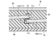
- FIG. 1A and FIG. 1B show a solar cell module M according to an embodiment.
- the solar cell module M includes the solar cell string 10, the sealing material layer 20 in which the solar cell string 10 is embedded in the middle portion in the thickness direction, and the light receiving surface side of the sealing material layer 20 A light receiving surface side protection member 30 and a back surface side protection member 40 stacked on the back surface side of the sealing material layer 20 are included.
- the solar cell string 10 connects a plurality of solar cells 11 mechanically and electrically.
- the plurality of solar cells 11 are in appearance as a string like yarn and they are electrically connected, they are referred to as solar cell strings 10.
- Each of the plurality of solar cells 11 includes an n-type or p-type semiconductor substrate 111 serving as a cell body, an n-type semiconductor layer (not shown), and a p-type semiconductor layer (not shown).
- the n-type semiconductor substrate 111 include a single crystal silicon substrate doped with an n-type dopant for introducing an electron into a silicon atom such as phosphorus.
- the p-type semiconductor substrate 111 include a single crystal silicon substrate in which a p-type dopant for introducing holes into a silicon atom such as boron is doped.
- one side main surface is the back surface, and the other side main surface opposite to that is the light receiving surface It is called respectively.
- stacked on the semiconductor substrate 111 and which doped the n-type dopant etc. are mentioned, for example.
- the p-type semiconductor layer include a silicon-based thin film layer doped with a p-type dopant and laminated on the semiconductor substrate 111.
- Each of the plurality of solar cells 11 is a first one of an n-type electrode electrically connected to the n-type semiconductor layer and a p-type electrode electrically connected to the p-type semiconductor layer on the back surface.
- An electrode 121 and the other second electrode 122 are provided.
- Such a solar battery cell 11 is called a "back contact type”.
- the first electrode 121 and the second electrode 122 collect carriers such as holes or electrons.
- the first electrode 121 and the second electrode 122 are preferably metal electrodes. However, it is not limited to this. In addition, a transparent conductive layer such as a metal oxide may be provided between the first electrode 121 and the second electrode 122 and the semiconductor layer that is the lower layer thereof.
- the first electrode 121 and the second electrode 122 of the metal electrode are formed by a known method such as printing or plating. Specifically, for example, an Ag electrode is formed by screen printing of Ag paste, and a copper plating electrode is formed by electrolytic plating.
- Each of the plurality of solar battery cells 11 preferably has a concavo-convex structure formed on the light receiving surface from the viewpoint of capturing a large amount of light and enhancing the conversion efficiency.
- the concavo-convex structure is preferably configured by an assembly of quadrangular pyramidal shapes (pyramid shapes).
- the pyramid-shaped uneven structure can be formed, for example, by subjecting the surface of the semiconductor substrate 111 to anisotropic etching.
- the height of the unevenness of the uneven structure is, for example, 0.5 ⁇ m or more and 10 ⁇ m or less, preferably 1 ⁇ m or more and 5 ⁇ m or less.
- the uneven structure may be formed on the back surface of the solar battery cell 11.
- Each of the plurality of solar cells 11 has one end 11a and the other end 11b arranged to extend in parallel.
- the back surface at one end 11a of one of the pair of solar cells 11A is at the other end 11b of the other solar cell 11B. It is disposed to overlap the light receiving surface, and is mechanically and electrically connected.
- Such connection is called a shingling connection because the solar cells 11 are arranged and connected as if roofing is covered with tiles.
- the overlapping width of the one end 11a of one solar cell 11A and the other end 11b of the other solar cell 11B is, for example, 0.5 mm or more and 3.0 mm or less.
- the first electrode 121 of one solar battery cell 11A and the second electrode 122 of the other solar battery cell 11B are electrically connected via the conductive connection member 50.
- the conductive connection member 50 is formed in a U-shaped cross section, in other words, a curved shape, by a strip-shaped metal foil of 10 ⁇ m to 100 ⁇ m.
- the metal material forming the metal foil is preferably a copper or a copper alloy containing copper as a main component, or an aluminum or an aluminum alloy containing aluminum as a main component, from the viewpoint of low cost.
- the metal foil forming the conductive connection member 50 may be plated with solder, tin, nickel or silver, or may be coated with a conductive paste or conductive adhesive.
- the conductive connecting member 50 is formed on the other end 11b of the other solar battery cell 11B on the lower side (for example, the back surface side of the solar battery module M) of the stacked solar battery cells 11A and 11B. It is arranged to cover. That is, the conductive connection member 50 extends from the back surface of the other solar cell 11B, which is one of the stacked solar cells 11A and 11B, toward the light receiving surface. And it is one end of conductive connecting member 50, and a part inside [curvature] is electrically connected to the 2nd electrode 122 of the back of other end 11b of other solar cell 11B via a connecting material. Be done.
- the conductive connection members 50 extending over both main surfaces of the other solar cell 11B are stacked solar cells on the back surface of the other solar cell 11B (that is, on both main surfaces of the other solar cell 11).
- a portion of the battery cells 11A and 11B facing the one main surface away from the solar battery cell 11A is connected to the second electrode 122 via the connection material.
- the other end with respect to one end which is a connection portion to the second electrode 122 of the back surface of the other end 11b of the other solar battery cell 11B is as follows. That is, the other end of the conductive connection member 50 and a part of the outer side of the warped shape are disposed on the upper side (for example, the light receiving surface side of the solar cell module M) of the stacked solar cells 11A and 11B. It is electrically connected to the 1st electrode 121 of the back of one end 11a of one photovoltaic cell 11A via a connection material.
- the conductive connection member 50 which is spread over both main surfaces of the other solar battery cell 11B has a portion facing the back surface of one solar battery cell 11A of the stacked solar battery cells 11A and 11B, It connects to the 1st electrode 121 of one solar cell 11A via a connection material.
- connection material examples include solder, solder paste containing solder particles, and conductive paste containing metal particles.
- connection material is not limited to this, and it is an insulating material if it can be connected so as to electrically connect the conductive connection member 50 and the electrode (first electrode 121 / second electrode 122). It may be a connecting material (for example, an adhesive).
- the conductivity type of the semiconductor substrate 111 which is the cell body of the solar battery cell 11 and the conductivity type of the semiconductor layer to which the second electrode 122 is electrically connected are the same. That is, when the semiconductor substrate 111 of the solar battery cell 11 is an n-type semiconductor substrate, the second electrode 122 on the back surface of the other end 11b of the other solar battery cell 11B disposed on the back surface side becomes an n-type electrode The 1st electrode 121 of the back of one end 11a of one photovoltaic cell 11A arranged at the side turns into a p type electrode.
- the semiconductor substrate 111 of the solar battery cell 11 is a p-type semiconductor substrate
- the second electrode 122 on the back surface of the other end 11b of the other solar battery cell 11B disposed on the back surface side becomes a p-type electrode
- the 1st electrode 121 of the back of one end 11a of one solar cell 11A arranged at the side turns into an n type electrode.
- the first electrode 121 of the back surface of one of the solar cells 11A disposed on the light receiving surface side and the first electrode 121 of the other solar cell 11B disposed on the back surface Even if the conductive connection member 50 is provided between the two electrodes 122 and the conductive connection member 50 is in contact with the semiconductor substrate 111 of the other solar battery cell 11B, the conductivity type of the semiconductor substrate 111 and Since the conductivity type of the semiconductor layer to which the two electrodes 122 are electrically connected is the same, a leak path does not occur and the shunt resistance does not decrease. As a result, high power generation efficiency can be obtained.
- the conductivity type of the semiconductor substrate 111 and the conductivity type of the semiconductor layer to which the second electrode 122 is electrically connected are preferably n-type.
- the high designability by which the connection structure of an electrode is not visually recognized from the light-receiving surface side is also obtained by shingling connection.
- the conductive connection member 50 is, as shown in FIG. 2A, a linear portion provided along one end portion 11a of one solar cell 11A in the first electrode 121 of the back surface of one solar cell 11A. Or as shown to FIG. 2B, you may electrically connect to the dotted
- the conductive connection member 50 is a linear member provided along the other end 11b of the other solar cell 11B in the second electrode 122 on the back surface of the other solar cell 11B. Or, as shown in FIG. 3B, may be electrically connected to a point-like portion provided along the other end 11b.
- an insulating buffer member 60 may be interposed between the conductive connection member 50 and the other solar battery cell 11B.
- the insulating buffer member 60 is provided so as to cover a part of the light receiving surface including the end of the other end 11b of the other solar battery cell 11B and a part of the side end surface.
- the pressure at the time of sealing of the solar battery string 10 in the sealing material layer 20 becomes conductive.
- the insulating connecting member 50 acts on the insulating connecting member 50, it acts as a cushion, and the conductive connecting member 50 contacts the other solar cell 11B to cause the solar cell 11B to crack. Suppress.
- the insulating buffer member 60 covers the end of the light receiving surface of the other end 11b of the other solar cell 11B.
- the insulating buffer member 60 is a member of one solar battery cell 11A overlapping the other end 11b of the other solar battery cell 11B by the action of pressure at the time of sealing of the solar battery string 10 in the sealing material layer 20. It is preferable that it is transparent from a viewpoint of suppressing the reduction
- the material of the insulating buffer member 60 include polyimide (PI), polyethylene terephthalate (PET), ethylene / vinyl acetate copolymer (EVA), acrylic resin, polyvinyl fluoride resin, and olefin resin.
- the solar battery cell 11 may be comprised by the division piece obtained by dividing
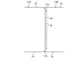
- FIG. 6 shows an example of the solar battery cell 11.
- the large-sized solar battery cell 11X is formed in a semi-square-type square shape having a side length of, for example, about 20 mm or more and about 200 mm or less and provided with the notch portions 13 at four corners.
- the solar battery cell 11 is obtained by dividing the large-sized solar battery cell 11X into two along a dividing line C1-C2 in the center of FIG. Therefore, the long side 14 has a length of, for example, about 20 mm to 200 mm, and the short side 15 has a length of, for example, about 10 mm to 100 mm. Notches 13 are provided at the corners.
- the divided solar battery cell 11 When the solar battery cell 11 obtained by dividing such a large-sized solar battery cell 11X is used to form the solar battery module M, the divided solar battery cell 11 has a smaller mounting area than the large-sized solar battery cell 11X. Many are implemented. That is, the mounting amount (power generation area) of the solar cells in the solar cell module M is increased. Therefore, the solar battery module M mounting the divided solar battery cells 11 can increase the amount of power generation more than the solar battery module M mounting the large-sized solar battery cells 11X.
- the large-sized solar battery cell 11X divides the surface of the large-sized semiconductor substrate 111X, which is the back surface, into two semiconductor substrates 111 for forming each solar battery cell 11, and the n-type region And a first conductivity type region which is one of p type regions and a second conductivity type region which is the other. Then, based on a known method, the first electrode 121 is provided on the first conductivity type region and the second electrode 122 is provided on the second conductivity type region. To form the first and second conductivity type regions, a technique of providing a doping region on the large-size semiconductor substrate 111X and a technique of forming a semiconductor thin film such as an amorphous silicon thin film on the large-size semiconductor substrate 111X are applied.
- an intrinsic semiconductor thin film such as an intrinsic amorphous silicon thin film is provided between the large format semiconductor substrate 111X and the conductive type semiconductor thin film.
- an intrinsic semiconductor thin film such as an intrinsic amorphous silicon thin film is provided between the large format semiconductor substrate 111X and the conductive type semiconductor thin film.
- the first electrode 121 and the second electrode 122 have a comb shape and be patterned so that the comb teeth mesh with each other.
- the first electrode 121 is formed in a comb shape having a plurality of first electrode finger portions 121a and a single first electrode bus bar portion 121b.
- Each of the plurality of first electrode finger portions 121 a extends in parallel to the short side 15 of the solar battery cell 11 and is disposed at an interval in the direction in which the long side 14 of the solar battery cell 11 extends.
- the first electrode bus bar portion 121b is connected to the long side 14 of the plurality of first electrode finger portions 121a so as to connect the end on the long side 14 side where the cutout portion 13 of the solar battery cell 11 is provided.
- the second electrode 122 is also formed in a comb shape having a plurality of second electrode finger portions 122a and a single second electrode bus bar portion 122b.
- Each of the plurality of second electrode finger portions 122 a extends in parallel to the short side 15 of the solar battery cell 11 and is arranged at intervals in the extending direction of the long side 14 of the solar battery cell 11.
- the second electrode bus bar portion 122 b is connected to the long side 14 of the plurality of second electrode finger portions 122 a so as to connect the end on the long side 14 side where the cutout portion 13 of the solar battery cell 11 is not provided. That is, it is provided to extend along the other end 11b.
- the first electrode 121 and the second electrode 122 are arranged such that the first electrode finger portion 121 a and the second electrode finger portion 122 a are alternately engaged in the extending direction of the long side 14 of the solar battery cell 11.
- the lengths of the first electrode finger portion 121a and the second electrode finger portion 122a are about half of the lengths of the first electrode bus bar portion 121b and the second electrode bus bar portion 122b, the first electrode finger portion 121a And, the carrier recovery loss due to the line resistance of the second electrode finger portion 122a is reduced.
- Conductive connection member 50 is preferably electrically connected to linear first electrode bus bar portion 121 b of first electrode 121 extending along one end 11 a of solar battery cell 11, and conductive connection member 50. Is preferably electrically connected to the linear second electrode bus bar portion 122 b of the second electrode 122 extending along the other end 11 b of the solar battery cell 11.
- the large-sized solar battery cell 11X is preferably designed so as to obtain two identical solar battery cells 11 by division. Therefore, it is preferable that the first conductivity type region and the second conductivity type region be patterned on the large-size semiconductor substrate 111X so as to be 180 ° rotational symmetric about the substrate center. As described above, when the same solar battery cell 11 is obtained from the large-sized solar battery cell 11X, handling of the solar battery cell 11 after division becomes easy by using the division end of the solar battery cell 11 as a clue. The workability when forming the string 10 is good. In particular, if a large-sized solar battery cell 11X formed in a semisquare square shape as shown in FIG. 5 is divided into two to obtain a solar battery cell 11 as shown in FIG.
- the first electrode bus bar portion 121b extends along the longer side 14 of the first electrode, and the second electrode bus bar portion 122b extends along the longer side 14 where the notch 13 is not provided. Since it can be easily identified, the handling of the photovoltaic cell 11 after division becomes easier.
- Examples of the method of dividing the large-sized solar battery cell 11X include laser processing.
- the large-sized solar battery cell 11X is divided into two by forming a groove by irradiating the large-sized solar battery cell 11X with laser light along the dividing line and breaking the groove as a fragile portion.
- the formation of the groove may be performed on either the light receiving surface side or the back surface side.
- the reflecting portion 16 is provided along the long side 14 on the light receiving surface of the one end portion 11a corresponding to the outer peripheral edge of the large format solar cell 11X. It may be provided.
- the film thickness of the semiconductor thin film becomes uneven at the outer peripheral edge.
- the outer peripheral edge of the large-sized solar battery cell 11X is highly likely to be rubbed or scratched on the surface in handling or the like at the time of its production. Therefore, in the solar battery cell 11 obtained from the large-sized solar battery cell 11X, the portion corresponding to the outer peripheral edge of the large-sized solar battery cell 11X has a larger power generation loss due to carrier recombination or the like than the portion corresponding to the central portion. The power generation efficiency tends to be relatively low.
- the reflection part 16 when the reflection part 16 is provided in the part of the light receiving surface side corresponding to the outer periphery of the large-sized solar battery cell 11X, the light irradiated to the area of the reflection part 16 is reflected by the reflection part 16 and the solar cell It does not enter the cell 11 directly.
- the light reflected by the reflecting portion 16 is re-reflected by another member or the like and contributes to power generation by being incident on the solar battery cell 11 from a region where the reflecting portion 16 is not provided. It is not necessary for the light to be incident on the solar battery cell 11 in which the light is reflected by the reflection part 16, and another solar battery cell 11 included in the solar battery string 10 may be used.
- the power generation loss due to the light entering the portion with low power generation efficiency corresponding to the outer peripheral edge of the large format solar battery cell 11X is reduced, and the light reflected by the reflection portion 16 is a region with high power generation efficiency High power generation output can be obtained by injecting the light into the normal region of the part).
- the reflection part 16 should just be provided in at least one part of the light-receiving surface side of the one end part 11a of one solar battery cell 11A, for example, as shown in FIG. It may be provided along both sides 15 and may be provided only along the short side 15 of the solar battery cell 11.
- the material of the reflective portion 16 is not particularly limited as long as it can reflect light, but a metal such as copper, aluminum, silver, gold, tin, or an alloy thereof is preferable because the reflectance is high. In addition, it is sufficient that the light receiving surface side of the reflecting unit 16 has light reflectivity, and the reflecting unit 16 may be formed of a reflecting member in which a reflecting layer such as metal is provided on the surface of a resin material.
- the reflecting portion 16 may be provided by printing a metal layer or the like, or may be provided by bonding a reflecting member.
- the reflecting portion 16 may be provided with asperities on the surface on the light receiving surface side in order to reflect light in an oblique direction and to increase the incident amount of the reflected light to other portions. From the same point of view, the reflecting portion 16 may have a surface inclined with respect to the light receiving surface of the solar battery cell 11. For example, as shown in FIG. The inclination angle of the inclined surface in the ridge of the reflecting section 16 which is continuous and may be formed to extend in the length direction (the extending direction of the short side 15) is set to a predetermined range.
- the incident angle of the light reflected by the reflecting portion 16 to the light receiving surface side protective member 30 is increased, and the reflectance at the interface between the light receiving surface side protective member 30 and the air is increased accordingly, and the reflective portion
- the light reflected by the light source 16 is reflected by the light receiving surface side protective member 30 and enters the solar battery cell 11, and the amount of light is increased to improve the power generation efficiency.
- the surface of the light receiving surface side may be formed to be a curved surface, for example, as shown in FIG. 9B, the reflecting portion 16 may be formed by a ridge having a semicircular cross section.
- the material of the sealing material layer 20 has high light transmissivity and high resistance to ultraviolet light. Moreover, it is preferable that the adhesiveness with the photovoltaic cell 11 contained in the solar cell string 10, the light-receiving surface side protection member 30, and the back surface side protection member 40 of the material of the sealing material layer 20 is high.
- the material of the encapsulant layer 20 include ethylene / vinyl acetate copolymer (EVA), ethylene / ⁇ -olefin copolymer, ethylene / vinyl acetate / trially isocyanurate (Evat), polyvinyl butyrate And light transmissive resins such as acrylic resins, urethane resins, and silicone resins.
- the sealing material layer 20 may be formed of a single material, or may be formed of different materials in the portion on the light receiving surface side and the portion on the back surface side of the solar cell string 10.
- the material of the encapsulating material layer 20 contains additives such as organic peroxide, silane coupling agent, ultraviolet absorber, wavelength conversion additive, crosslinking assistant, heat resistant stabilizer, light resistant stabilizer and the like. It is also good.
- the material of the light receiving surface side protective member 30 has high light transmissivity and high resistance to ultraviolet light.
- the material of the light receiving surface side protective member 30 include glass, and transparent resin such as acrylic resin or polycarbonate resin. Asperities may be provided on the surface of the light receiving surface side of the light receiving surface side protective member 30.
- the surface on the light receiving surface side of the light receiving surface side protective member 30 may be coated with an antireflective coating layer. When such an antireflective coating layer is provided, reflection of light is suppressed and more light can be guided to the solar battery cell 11.
- the material of the back surface side protective member 40 has high water permeability so as to restrict the infiltration of water or the like.
- the material of the back side protection member 40 include olefin resins such as polyethylene terephthalate (PET) and polyethylene (PE), fluorine-containing resins, silicone-containing resins, and the like.
- the back surface side protection member 40 may have light reflectivity.
- the light-reflecting back surface side protective member 40 preferably exhibits a metallic color or a white color, and may be formed of, for example, a white resin film or a laminate in which a metal foil such as aluminum is sandwiched between resin films.
- the back surface side protection member 40 may have light absorbency.
- the back side protection member 40 having light absorbability is formed of a black resin layer or the like whose appearance is black. If a black one is used as the back side protection member 40, the appearance color is similar to that of the solar cell string 10 including the plurality of solar cells 11, and thus the solar cell module M with high designability is unified in black on the entire surface. Become. In addition, the back surface side protection member 40 may have light transmittance.
- the solar cell module M is a sheet material that forms the light receiving surface side protection member 30 after forming the solar cell string 10 by connecting the plurality of solar battery cells 11 using the conductive connection member 50, and a seal A sheet material which forms a portion on the light receiving surface side of the fixing material layer 20, a solar cell string 10, a sheet material which forms a portion on the back surface side of the sealing material layer 20, and a lamination in which a back surface side protection member 40 is overlapped in this order
- the body is manufactured by heating and pressurizing at a predetermined temperature and pressure using a laminator or the like which performs evacuation.
- Example 1 First, in a solar cell similar to that shown in FIG. 6, a plurality of n-type single crystal silicon substrates are used as a semiconductor substrate, a first electrode is a p-type electrode, and a second electrode is an n-type electrode.
- a first electrode is a p-type electrode
- a second electrode is an n-type electrode.
- To create multiple solar cell strings (see FIGS. 1A and 1B).
- each solar cell string in any pair of solar cells adjacent to each other, one end of one of them is provided so as to overlap 1.5 mm on the light receiving surface side of the other end of the other, and one end Solder the conductive connecting members made of 50- ⁇ m-thick band-like copper foil to the first electrode bus bar on the back of the second part and the second electrode bus bar on the back on the other end of the other part. Electrically connected.
- the sheet material forming the light receiving surface side protective member and the sheet material forming the portion on the light receiving surface side of the sealing material layer are laminated in order, and the plurality of solar cell strings produced in the width direction The spacing was 3 mm.
- the adjacent string ends were electrically connected such that the plurality of solar cell strings continued in a ninety nine-fold manner, whereby all the solar cells were connected in series.
- the sheet material which forms the part by the side of the back of a sealing agent layer on a plurality of solar cell strings, and the back side protection member were piled up in order, and the layered product was obtained.
- the laminated body is subjected to thermocompression bonding for 5 minutes under atmospheric pressure, and then held at 150 ° C. for 60 minutes to crosslink the sealing material layer, as shown in FIGS. 1A and 1B.
- a solar cell module of Example 1 similar to that shown in was produced.
- Sheet material for forming the light receiving surface side protection member White sheet glass, sheet material for forming the light receiving surface side portion and the back surface side portion of the sealing material layer EVA sheet, and sheet material forming the back surface side protection member
- a laminated sheet of a PET sheet and a black resin layer was used.
- Example 2 A solar cell module of Example 2 similar to that shown in FIG. 4 was produced, except that an insulating buffer member was interposed between the conductive connection member and the other solar battery cell. did. Here, an EVA sheet was used as the insulating buffer member.
- Example 7 is the same as Example 2 shown in FIGS. 7A and 7B except that a reflection part extending along the long side is provided on the light receiving surface side of one end of one solar cell.
- a solar cell module was produced.
- a light diffusion tab wiring of 2 mm in width in which the surface of the copper foil on which the concavo-convex structure was formed was coated with silver was used for the reflective portion.
- Comparative Example As a solar cell, a solar cell module of the same comparative example as in Example 1 was produced except that the first electrode was an n-type electrode and the second electrode was a p-type electrode.
- Test evaluation result The test evaluation results are shown in Table 1.
- Example 1 has a higher fill factor (FF).
- the conductive connecting member for electrically connecting the n-type electrode on the back surface of the solar cell on the light receiving surface side to the p-type electrode on the back surface of the solar cell on the back surface is the solar cell on the back surface It is considered that the occurrence of a leak path in contact with the n-type single crystal silicon substrate of (1) lowers the shunt resistance, thereby causing a reduction in performance.
- Example 1 the conductive connecting member for electrically connecting the p-type electrode on the back surface of the solar cell on the light receiving surface side and the n-type electrode on the back surface of the solar cell on the back surface Even when the solar cell is in contact with the n-type single crystal silicon substrate of the side solar cell, since the conductivity type is all n-type, it is considered that the shunt resistance is kept high without generating a leak path.
- Example 2 has a higher fill factor (FF).
- FF fill factor
- Example 2 when the insulating buffer member is provided between the conductive connection member and the other solar cell on the back surface side, when the solar cell string is sealed in the sealing material layer The insulating cushioning member plays the role of a cushion even if the pressure of Thereby, generation
- Example 3 has a higher maximum output (Pmax). This is because, in the third embodiment, since the reflection portion is provided on the light receiving surface side of one end of the solar battery cell corresponding to the outer peripheral edge of the large-sized solar battery cell having relatively low power generation efficiency, the power generation efficiency is relatively It is considered that a higher output than in Example 2 can be obtained because the amount of light incident on the high region increases.
Abstract
This solar battery module (M) comprises a plurality of solar battery cells (11A, 11B). The solar battery cells (11A, 11B) include an n type or p type semiconductor substrate (111). On a primary surface of one side of the semiconductor substrate (111) are provided a first electrode (121) connected to one of the n type semiconductor layer and the p type semiconductor layer, and a second electrode (122) connected to the other. A primary surface of one side on one end part (11a) of one of the pair of solar battery cells (11A, 11B) overlaps the primary surface of the other side of another end part (11b) of the other of the pair of solar battery cells (11A, 11B). The first electrode (121) of the one of the pair of solar battery cells (11A, 11B) and the second electrode (122) of the other of the pair of solar battery cells (11A, 11B) are connected with an electrically conductive connection member (50) interposed. The electrically conductive type of the semiconductor substrate (111) and the electrically conductive type of the semiconductor layer that is electrically connected to the second electrode (122) are the same.
Description
本発明は、太陽電池モジュールに関する。
The present invention relates to a solar cell module.
単一の太陽電池セルだけでは、面積が小さいために高出力を得ることができない。そのため、通常、複数の太陽電池セルを電気的に接続して連ねた太陽電池モジュールとして高出力化を図っている。例えば、特許文献1には、受光面とは反対側の裏面にn型電極及びp型電極の両方が設けられた裏面電極型の複数の太陽電池セルを備え、それらの複数の太陽電池セルの一端部及び他端部を重ねてシングリング接続した太陽電池モジュールが開示されている。
With a single solar cell alone, high output can not be obtained because the area is small. Therefore, high output is usually achieved as a solar cell module in which a plurality of solar cells are electrically connected and connected. For example, Patent Document 1 includes a plurality of back surface electrode type solar cells in which both an n-type electrode and a p-type electrode are provided on the back surface opposite to the light receiving surface. A solar cell module is disclosed in which one end and the other end are stacked and shingled.
本発明は、電気的に接続されて連なる複数の太陽電池セルを備えた太陽電池モジュールであって、前記複数の太陽電池セルのそれぞれは、n型又はp型の半導体基板と、n型半導体層と、p型半導体層とを含むとともに、前記半導体基板における一方側主面及び他方側主面のうちの前記一方側主面に、前記n型半導体層に電気的に接続されたn型電極及び前記p型半導体層に電気的に接続されたp型電極のうちの一方である第1電極及び他方である第2電極が設けられ、且つ並行に延びるように配置された一端部及び他端部を有しており、前記複数の太陽電池セルのうちの相互に隣接する任意の一対において、前記一対のうちの一方の太陽電池セルの前記一端部における前記一方側主面が、他方の太陽電池セルの前記他端部における前記他方側主面に重ねられるとともに、前記一方の太陽電池セルの前記第1電極と前記他方の太陽電池セルの前記第2電極とが導電性接続部材を介して電気的に接続されており、前記半導体基板の導電型と、前記第2電極に電気的に接続された半導体層の導電型とが同一である。
The present invention is a solar cell module including a plurality of solar cells electrically connected and connected, wherein each of the plurality of solar cells is an n-type or p-type semiconductor substrate, an n-type semiconductor layer An n-type electrode electrically connected to the n-type semiconductor layer, the p-type semiconductor layer being electrically connected to the one-side main surface of the one-side main surface and the other-side main surface of the semiconductor substrate; One end and the other end provided with a first electrode that is one of the p-type electrodes electrically connected to the p-type semiconductor layer and a second electrode that is the other, and extending in parallel In one of the plurality of solar cells adjacent to each other, the one main surface of the one end portion of one of the solar cells of the pair is the other solar cell The other at the other end of the cell The first electrode of the one solar cell and the second electrode of the other solar cell are electrically connected to each other through the conductive connection member while being overlapped on the side main surface. The conductivity type of the substrate and the conductivity type of the semiconductor layer electrically connected to the second electrode are the same.
以下、実施形態について詳細に説明する。
Hereinafter, the embodiment will be described in detail.
図1A及び図1Bは、実施形態に係る太陽電池モジュールMを示す。
FIG. 1A and FIG. 1B show a solar cell module M according to an embodiment.
実施形態に係る太陽電池モジュールMは、太陽電池ストリング10と、その太陽電池ストリング10を厚さ方向の中間部に埋め込む封止材層20と、その封止材層20の受光面側に積み重ねた受光面側保護部材30と、封止材層20の裏面側に積み重ねた裏面側保護部材40とを含む。
The solar cell module M according to the embodiment includes the solar cell string 10, the sealing material layer 20 in which the solar cell string 10 is embedded in the middle portion in the thickness direction, and the light receiving surface side of the sealing material layer 20 A light receiving surface side protection member 30 and a back surface side protection member 40 stacked on the back surface side of the sealing material layer 20 are included.
太陽電池ストリング10は、複数の太陽電池セル11を機械的かつ電気的に接続して連ねる。換言すると、複数の太陽電池セル11が、外観上、糸のように一連状になっており、電気的に接続されていれば、それを太陽電池ストリング10と称する。
The solar cell string 10 connects a plurality of solar cells 11 mechanically and electrically. In other words, if the plurality of solar cells 11 are in appearance as a string like yarn and they are electrically connected, they are referred to as solar cell strings 10.
複数の太陽電池セル11のそれぞれは、セル本体となるn型又はp型の半導体基板111と、n型半導体層(不図示)と、p型半導体層(不図示)とを含む。n型の半導体基板111としては、例えば、リンのようなシリコン原子に電子を導入するためのn型ドーパントをドープした単結晶シリコン基板等が挙げられる。p型の半導体基板111としては、例えば、ホウ素のようなシリコン原子に正孔を導入するためのp型ドーパントをドープした単結晶シリコン基板等が挙げられる。なお、以下では、太陽電池セル11及び半導体基板111における一方側主面及び他方側主面の2つの主面のうち、一方側主面を裏面、及びその反対側の他方側主面を受光面とそれぞれ称する。
Each of the plurality of solar cells 11 includes an n-type or p-type semiconductor substrate 111 serving as a cell body, an n-type semiconductor layer (not shown), and a p-type semiconductor layer (not shown). Examples of the n-type semiconductor substrate 111 include a single crystal silicon substrate doped with an n-type dopant for introducing an electron into a silicon atom such as phosphorus. Examples of the p-type semiconductor substrate 111 include a single crystal silicon substrate in which a p-type dopant for introducing holes into a silicon atom such as boron is doped. In addition, below, among the two main surfaces of one side main surface and the other side main surface in the solar battery cell 11 and the semiconductor substrate 111, one side main surface is the back surface, and the other side main surface opposite to that is the light receiving surface It is called respectively.
n型半導体層としては、例えば、半導体基板111に積層された、n型ドーパントをドープしたシリコン系薄膜層等が挙げられる。p型半導体層としては、例えば、半導体基板111に積層された、p型ドーパントをドープしたシリコン系薄膜層等が挙げられる。
As an n-type semiconductor layer, the silicon-type thin film layer etc. which were laminated | stacked on the semiconductor substrate 111 and which doped the n-type dopant etc. are mentioned, for example. Examples of the p-type semiconductor layer include a silicon-based thin film layer doped with a p-type dopant and laminated on the semiconductor substrate 111.
複数の太陽電池セル11のそれぞれは、裏面に、n型半導体層に電気的に接続されたn型電極及びp型半導体層に電気的に接続されたp型電極のうちの一方である第1電極121及び他方である第2電極122が設けられる。このような太陽電池セル11は、「バックコンタクト型」と称される。第1電極121及び第2電極122は、正孔または電子といったキャリアを回収する。
Each of the plurality of solar cells 11 is a first one of an n-type electrode electrically connected to the n-type semiconductor layer and a p-type electrode electrically connected to the p-type semiconductor layer on the back surface. An electrode 121 and the other second electrode 122 are provided. Such a solar battery cell 11 is called a "back contact type". The first electrode 121 and the second electrode 122 collect carriers such as holes or electrons.
第1電極121及び第2電極122は、金属電極であると好ましい。ただし、これに限定されるものではない。また、第1電極121及び第2電極122と、それらの下層である半導体層との間には、金属酸化物等の透明導電層が設けられていてもよい。金属電極の第1電極121及び第2電極122は、印刷またはメッキ等の公知の方法により形成される。具体的には、例えば、Ag電極は、Agペーストのスクリーン印刷により形成され、銅メッキ電極は、電解メッキにより形成される。
The first electrode 121 and the second electrode 122 are preferably metal electrodes. However, it is not limited to this. In addition, a transparent conductive layer such as a metal oxide may be provided between the first electrode 121 and the second electrode 122 and the semiconductor layer that is the lower layer thereof. The first electrode 121 and the second electrode 122 of the metal electrode are formed by a known method such as printing or plating. Specifically, for example, an Ag electrode is formed by screen printing of Ag paste, and a copper plating electrode is formed by electrolytic plating.
複数の太陽電池セル11のそれぞれは、多くの光を取り込むとともに、その変換効率を高める観点から、受光面に凹凸構造が形成されていることが好ましい。凹凸構造は、四角錐形状(ピラミッド形状)の集合体で構成されていることが好ましい。ピラミッド形状の凹凸構造は、例えば、半導体基板111の表面に異方性エッチング処理を施すことにより形成することができる。凹凸構造の凹凸の高さは、例えば0.5μm以上10μm以下であり、好ましくは1μm以上5μm以下である。なお、太陽電池セル11の裏面にも凹凸構造が形成されていてもよい。
Each of the plurality of solar battery cells 11 preferably has a concavo-convex structure formed on the light receiving surface from the viewpoint of capturing a large amount of light and enhancing the conversion efficiency. The concavo-convex structure is preferably configured by an assembly of quadrangular pyramidal shapes (pyramid shapes). The pyramid-shaped uneven structure can be formed, for example, by subjecting the surface of the semiconductor substrate 111 to anisotropic etching. The height of the unevenness of the uneven structure is, for example, 0.5 μm or more and 10 μm or less, preferably 1 μm or more and 5 μm or less. In addition, the uneven structure may be formed on the back surface of the solar battery cell 11.
複数の太陽電池セル11のそれぞれは、並行に延びるように配置された一端部11a及び他端部11bを有する。複数の太陽電池セル11のうちの相互に隣接する任意の一対において、それらの一対のうちの一方の太陽電池セル11Aの一端部11aにおける裏面が、他方の太陽電池セル11Bの他端部11bにおける受光面に重なるように配置され、機械的かつ電気的に接続される。このように、屋根に瓦を葺いたように、太陽電池セル11を配置、接続させていることから、このような接続は、シングリング接続と称される。なお、一方の太陽電池セル11Aの一端部11a及び他方の太陽電池セル11Bの他端部11bの重なり幅は、例えば0.5mm以上3.0mm以下である。
Each of the plurality of solar cells 11 has one end 11a and the other end 11b arranged to extend in parallel. In an arbitrary pair of the plurality of solar cells 11 that are adjacent to each other, the back surface at one end 11a of one of the pair of solar cells 11A is at the other end 11b of the other solar cell 11B. It is disposed to overlap the light receiving surface, and is mechanically and electrically connected. Thus, such connection is called a shingling connection because the solar cells 11 are arranged and connected as if roofing is covered with tiles. The overlapping width of the one end 11a of one solar cell 11A and the other end 11b of the other solar cell 11B is, for example, 0.5 mm or more and 3.0 mm or less.
一方の太陽電池セル11Aの第1電極121と他方の太陽電池セル11Bの第2電極122とは、導電性接続部材50を介して電気的に接続されている。導電性接続部材50は、例えば10μm以上100μm以下の帯状の金属箔により断面U字状、換言すると、反り返った形状に形成されている。この金属箔を形成する金属材料は、低コストであるという観点から、銅若しくは銅を主成分とする銅合金、または、アルミニウム若しくはアルミニウムを主成分とするアルミニウム合金が好ましい。導電性接続部材50を形成する金属箔は、はんだ、錫、ニッケル、または銀でメッキされていてもよいし、導電性ペースト、または導電性接着剤で被覆されていてもよい。
The first electrode 121 of one solar battery cell 11A and the second electrode 122 of the other solar battery cell 11B are electrically connected via the conductive connection member 50. The conductive connection member 50 is formed in a U-shaped cross section, in other words, a curved shape, by a strip-shaped metal foil of 10 μm to 100 μm. The metal material forming the metal foil is preferably a copper or a copper alloy containing copper as a main component, or an aluminum or an aluminum alloy containing aluminum as a main component, from the viewpoint of low cost. The metal foil forming the conductive connection member 50 may be plated with solder, tin, nickel or silver, or may be coated with a conductive paste or conductive adhesive.
導電性接続部材50は、反り返り形状の内側を、積み重なった太陽電池セル11A,11B同士のうち下側(例えば、太陽電池モジュールMの裏面側)の他方の太陽電池セル11Bの他端部11bに被せるように配置される。すなわち、導電性接続部材50は、積み重なった太陽電池セル11A,11B同士のうちの1つである他方の太陽電池セル11Bにおける裏面から受光面に向かって掛け渡る。そして、導電性接続部材50の一端であって反り返り形状の内側の一部は、他方の太陽電池セル11Bの他端部11bの裏面の第2電極122に、接続材を介して電気的に接続される。つまり、他方の太陽電池セル11Bの両主面に掛け渡った導電性接続部材50は、その他方の太陽電池セル11Bの裏面(すなわち、他方の太陽電池セル11の両主面において、積み重なった太陽電池セル11A,11B同士のうちの一方の太陽電池セル11Aから乖離する側の主面)に対向する部分を、接続材を介して、第2電極122に接続する。
The conductive connecting member 50 is formed on the other end 11b of the other solar battery cell 11B on the lower side (for example, the back surface side of the solar battery module M) of the stacked solar battery cells 11A and 11B. It is arranged to cover. That is, the conductive connection member 50 extends from the back surface of the other solar cell 11B, which is one of the stacked solar cells 11A and 11B, toward the light receiving surface. And it is one end of conductive connecting member 50, and a part inside [curvature] is electrically connected to the 2nd electrode 122 of the back of other end 11b of other solar cell 11B via a connecting material. Be done. That is, the conductive connection members 50 extending over both main surfaces of the other solar cell 11B are stacked solar cells on the back surface of the other solar cell 11B (that is, on both main surfaces of the other solar cell 11). A portion of the battery cells 11A and 11B facing the one main surface away from the solar battery cell 11A is connected to the second electrode 122 via the connection material.
また、導電性接続部材50において、他方の太陽電池セル11Bの他端部11bの裏面の第2電極122への接続個所である一端に対する他端は、以下のようにされる。すなわち、導電性接続部材50の他端であって反り返り形状の外側の一部は、積み重なった太陽電池セル11A,11B同士のうち上側(例えば、太陽電池モジュールMの受光面側)に配置された一方の太陽電池セル11Aの一端部11aの裏面の第1電極121に、接続材を介して電気的に接続される。換言すると、他方の太陽電池セル11Bの両主面に掛け渡った導電性接続部材50は、積み重なった太陽電池セル11A,11B同士のうちの一方の太陽電池セル11Aの裏面に対向する部分を、接続材を介して、その一方の太陽電池セル11Aの第1電極121に接続する。
Moreover, in the conductive connection member 50, the other end with respect to one end which is a connection portion to the second electrode 122 of the back surface of the other end 11b of the other solar battery cell 11B is as follows. That is, the other end of the conductive connection member 50 and a part of the outer side of the warped shape are disposed on the upper side (for example, the light receiving surface side of the solar cell module M) of the stacked solar cells 11A and 11B. It is electrically connected to the 1st electrode 121 of the back of one end 11a of one photovoltaic cell 11A via a connection material. In other words, the conductive connection member 50 which is spread over both main surfaces of the other solar battery cell 11B has a portion facing the back surface of one solar battery cell 11A of the stacked solar battery cells 11A and 11B, It connects to the 1st electrode 121 of one solar cell 11A via a connection material.
なお、接続材としては、例えば、はんだ、はんだ粒子を含有するはんだペースト、金属粒子を含有する導電性ペースト等が挙げられる。ただし、接続材は、これに限定されるものではなく、導電性接続部材50と、電極(第1電極121/第2電極122)とを導通させるように接続させられるのであれば、絶縁性の接続材(例えば接着剤)であっても構わない。
Examples of the connection material include solder, solder paste containing solder particles, and conductive paste containing metal particles. However, the connection material is not limited to this, and it is an insulating material if it can be connected so as to electrically connect the conductive connection member 50 and the electrode (first electrode 121 / second electrode 122). It may be a connecting material (for example, an adhesive).
実施形態に係る太陽電池モジュールMでは、太陽電池セル11のセル本体である半導体基板111の導電型と、第2電極122が電気的に接続された半導体層の導電型とが同一である。すなわち、太陽電池セル11の半導体基板111がn型半導体基板のとき、裏面側に配置された他方の太陽電池セル11Bの他端部11bの裏面の第2電極122はn型電極となり、受光面側に配置された一方の太陽電池セル11Aの一端部11aの裏面の第1電極121はp型電極となる。また、太陽電池セル11の半導体基板111がp型半導体基板のとき、裏面側に配置された他方の太陽電池セル11Bの他端部11bの裏面の第2電極122はp型電極となり、受光面側に配置された一方の太陽電池セル11Aの一端部11aの裏面の第1電極121はn型電極となる。
In the solar cell module M according to the embodiment, the conductivity type of the semiconductor substrate 111 which is the cell body of the solar battery cell 11 and the conductivity type of the semiconductor layer to which the second electrode 122 is electrically connected are the same. That is, when the semiconductor substrate 111 of the solar battery cell 11 is an n-type semiconductor substrate, the second electrode 122 on the back surface of the other end 11b of the other solar battery cell 11B disposed on the back surface side becomes an n-type electrode The 1st electrode 121 of the back of one end 11a of one photovoltaic cell 11A arranged at the side turns into a p type electrode. When the semiconductor substrate 111 of the solar battery cell 11 is a p-type semiconductor substrate, the second electrode 122 on the back surface of the other end 11b of the other solar battery cell 11B disposed on the back surface side becomes a p-type electrode The 1st electrode 121 of the back of one end 11a of one solar cell 11A arranged at the side turns into an n type electrode.
実施形態に係る太陽電池モジュールMによれば、受光面側に配置された一方の太陽電池セル11Aの裏面の第1電極121と、裏面側に配置された他方の太陽電池セル11Bの裏面の第2電極122との間に導電性接続部材50が設けられ、その導電性接続部材50が他方の太陽電池セル11Bの半導体基板111に接触することがあっても、半導体基板111の導電型と第2電極122が電気的に接続された半導体層の導電型とが同一であるので、リークパスが発生してシャント抵抗が低下することもなく、その結果、高い発電効率が得られる。このような高い発電効率を得る観点からは、半導体基板111の導電型及び第2電極122が電気的に接続された半導体層の導電型はn型であることが好ましい。また、実施形態に係る太陽電池モジュールMによれば、シングリング接続により、受光面側から電極の接続構造が視認されない高い意匠性も得られる。
According to the solar cell module M according to the embodiment, the first electrode 121 of the back surface of one of the solar cells 11A disposed on the light receiving surface side and the first electrode 121 of the other solar cell 11B disposed on the back surface Even if the conductive connection member 50 is provided between the two electrodes 122 and the conductive connection member 50 is in contact with the semiconductor substrate 111 of the other solar battery cell 11B, the conductivity type of the semiconductor substrate 111 and Since the conductivity type of the semiconductor layer to which the two electrodes 122 are electrically connected is the same, a leak path does not occur and the shunt resistance does not decrease. As a result, high power generation efficiency can be obtained. From the viewpoint of obtaining such high power generation efficiency, the conductivity type of the semiconductor substrate 111 and the conductivity type of the semiconductor layer to which the second electrode 122 is electrically connected are preferably n-type. Moreover, according to the solar cell module M which concerns on embodiment, the high designability by which the connection structure of an electrode is not visually recognized from the light-receiving surface side is also obtained by shingling connection.
導電性接続部材50は、図2Aに示すように、一方の太陽電池セル11Aの裏面の第1電極121における一方の太陽電池セル11Aの一端部11aに沿うように設けられた線状の部分、又は、図2Bに示すように、一端部11aに沿うように設けられた点状の部分に電気的に接続されていてもよい。また、導電性接続部材50は、図3Aに示すように、他方の太陽電池セル11Bの裏面の第2電極122における他方の太陽電池セル11Bの他端部11bに沿うように設けられた線状の部分、又は、図3Bに示すように、他端部11bに沿うように設けられた点状の部分に電気的に接続されていてもよい。
The conductive connection member 50 is, as shown in FIG. 2A, a linear portion provided along one end portion 11a of one solar cell 11A in the first electrode 121 of the back surface of one solar cell 11A. Or as shown to FIG. 2B, you may electrically connect to the dotted | punctate part provided along the one end part 11a. In addition, as shown in FIG. 3A, the conductive connection member 50 is a linear member provided along the other end 11b of the other solar cell 11B in the second electrode 122 on the back surface of the other solar cell 11B. Or, as shown in FIG. 3B, may be electrically connected to a point-like portion provided along the other end 11b.
導電性接続部材50と他方の太陽電池セル11Bとの間には、図4に示すように、絶縁性緩衝部材60が介在されていてもよい。絶縁性緩衝部材60は、他方の太陽電池セル11Bの他端部11bの端を含む受光面の一部及び側端面の一部を覆うように設けられている。このように導電性接続部材50と他方の太陽電池セル11Bとの間に絶縁性緩衝部材60が介在されていると、太陽電池ストリング10の封止材層20内への封入時の圧力が導電性接続部材50に作用しても、絶縁性緩衝部材60がクッションの役割を果たし、導電性接続部材50が他方の太陽電池セル11Bに接触して、その太陽電池セル11Bにクラックを生じさせることを抑制する。しかも、他方の太陽電池セル11Bの他端部11bの端には大きな力が作用するので、絶縁性緩衝部材60が、その他方の太陽電池セル11Bの他端部11bの受光面の端を覆うように設けられていることにより、特に高いクラック抑制効果を得ることができる。
As shown in FIG. 4, an insulating buffer member 60 may be interposed between the conductive connection member 50 and the other solar battery cell 11B. The insulating buffer member 60 is provided so as to cover a part of the light receiving surface including the end of the other end 11b of the other solar battery cell 11B and a part of the side end surface. Thus, when the insulating buffer member 60 is interposed between the conductive connection member 50 and the other solar battery cell 11B, the pressure at the time of sealing of the solar battery string 10 in the sealing material layer 20 becomes conductive. Even if the insulating connecting member 50 acts on the insulating connecting member 50, it acts as a cushion, and the conductive connecting member 50 contacts the other solar cell 11B to cause the solar cell 11B to crack. Suppress. Moreover, since a large force acts on the end of the other end 11b of the other solar cell 11B, the insulating buffer member 60 covers the end of the light receiving surface of the other end 11b of the other solar cell 11B. By being provided as described above, a particularly high crack suppressing effect can be obtained.
絶縁性緩衝部材60は、太陽電池ストリング10の封止材層20内への封入時の圧力の作用により、他方の太陽電池セル11Bの他端部11bに重なっている一方の太陽電池セル11Aの一端部11aからはみ出すことによる受光量の減少を抑止する観点から、透明であることが好ましい。絶縁性緩衝部材60の材料としては、例えば、ポリイミド(PI)、ポリエチレンテレフタレート(PET)、エチレン/酢酸ビニル共重合体(EVA)、アクリル樹脂、ポリフッ化ビニル樹脂、オレフィン系樹脂等が挙げられる。
The insulating buffer member 60 is a member of one solar battery cell 11A overlapping the other end 11b of the other solar battery cell 11B by the action of pressure at the time of sealing of the solar battery string 10 in the sealing material layer 20. It is preferable that it is transparent from a viewpoint of suppressing the reduction | decrease of the light reception amount by protruding from the one end part 11a. Examples of the material of the insulating buffer member 60 include polyimide (PI), polyethylene terephthalate (PET), ethylene / vinyl acetate copolymer (EVA), acrylic resin, polyvinyl fluoride resin, and olefin resin.
太陽電池セル11は、図5に示すような大判太陽電池セル11Xを分割することにより得られる分割片で構成されていてもよい。図6は、その太陽電池セル11の一例を示す。
The solar battery cell 11 may be comprised by the division piece obtained by dividing | segmenting the large sized solar battery cell 11X as shown in FIG. FIG. 6 shows an example of the solar battery cell 11.
大判太陽電池セル11Xは、一辺の長さが例えば20mm以上200mm以下程度で、且つ4つの角に切り欠き部13が設けられたセミスクエア型の正方形状に形成されている。太陽電池セル11は、この大判太陽電池セル11Xを図5中央の分割線C1-C2で2分割して得られる。したがって、長辺14の長さが例えば20mm以上200mm以下程度、短辺15の長さがその半分の例えば10mm以上100mm以下程度の長方形状に形成され、また、もう一方の長辺14の両端の角に切り欠き部13が設けられている。このような大判太陽電池セル11Xを分割した太陽電池セル11が太陽電池モジュールMの形成に用いられる場合、その分割した太陽電池セル11は、限られた実装面積において、大判太陽電池セル11Xよりも多く実装される。つまり、太陽電池モジュールMにおける太陽電池の実装量(発電面積)が大きくなる。したがって、分割した太陽電池セル11を実装した太陽電池モジュールMは、大判太陽電池セル11Xを実装した太陽電池モジュールMよりも、発電量を高められる。
The large-sized solar battery cell 11X is formed in a semi-square-type square shape having a side length of, for example, about 20 mm or more and about 200 mm or less and provided with the notch portions 13 at four corners. The solar battery cell 11 is obtained by dividing the large-sized solar battery cell 11X into two along a dividing line C1-C2 in the center of FIG. Therefore, the long side 14 has a length of, for example, about 20 mm to 200 mm, and the short side 15 has a length of, for example, about 10 mm to 100 mm. Notches 13 are provided at the corners. When the solar battery cell 11 obtained by dividing such a large-sized solar battery cell 11X is used to form the solar battery module M, the divided solar battery cell 11 has a smaller mounting area than the large-sized solar battery cell 11X. Many are implemented. That is, the mounting amount (power generation area) of the solar cells in the solar cell module M is increased. Therefore, the solar battery module M mounting the divided solar battery cells 11 can increase the amount of power generation more than the solar battery module M mounting the large-sized solar battery cells 11X.
大判太陽電池セル11Xは、その裏面となる大判半導体基板111Xの表面を、各太陽電池セル11を作り込むための2つの半導体基板111となる領域に分け、それぞれに、半導体積層手段によってn型領域及びp型領域のうちの一方である第1導電型領域及び他方である第2導電型領域を設ける。そして、公知の方法に基づいて、第1導電型領域上に第1電極121及び第2導電型領域上に第2電極122をそれぞれ設ける。第1及び第2導電型領域の形成には、大判半導体基板111Xにドーピング領域を設ける技術、大判半導体基板111X上に非晶質シリコン薄膜等の半導体薄膜を形成する技術が適用される。なお、大判半導体基板111X上にn型又はp型の導電型半導体薄膜が設けられる場合、大判半導体基板111Xと導電型半導体薄膜との間に、真性非晶質シリコン薄膜等の真性半導体薄膜が設けられることにより、大判半導体基板111Xの表面のパッシベーション効果を得られる。
The large-sized solar battery cell 11X divides the surface of the large-sized semiconductor substrate 111X, which is the back surface, into two semiconductor substrates 111 for forming each solar battery cell 11, and the n-type region And a first conductivity type region which is one of p type regions and a second conductivity type region which is the other. Then, based on a known method, the first electrode 121 is provided on the first conductivity type region and the second electrode 122 is provided on the second conductivity type region. To form the first and second conductivity type regions, a technique of providing a doping region on the large-size semiconductor substrate 111X and a technique of forming a semiconductor thin film such as an amorphous silicon thin film on the large-size semiconductor substrate 111X are applied. When an n-type or p-type conductive semiconductor thin film is provided on the large format semiconductor substrate 111X, an intrinsic semiconductor thin film such as an intrinsic amorphous silicon thin film is provided between the large format semiconductor substrate 111X and the conductive type semiconductor thin film. Thus, the passivation effect of the surface of the large-sized semiconductor substrate 111X can be obtained.
第1電極121及び第2電極122は、各々が櫛形状であって、互いに櫛歯が噛み合うようにパターニングされると好ましい。具体的には、第1電極121は、複数本の第1電極フィンガー部分121aと、1本の第1電極バスバー部分121bとを有する櫛形状に形成されている。複数本の第1電極フィンガー部分121aは、各々が太陽電池セル11の短辺15に並行に延びるとともに、太陽電池セル11の長辺14の延びる方向に間隔をおいて配置されている。第1電極バスバー部分121bは、複数本の第1電極フィンガー部分121aの太陽電池セル11の切り欠き部13が設けられている方の長辺14側の端を連結するように、その長辺14、すなわち、一端部11aに沿って延びるように設けられている。第2電極122も、複数本の第2電極フィンガー部分122aと、1本の第2電極バスバー部分122bとを有する櫛形状に形成されている。複数本の第2電極フィンガー部分122aは、各々が太陽電池セル11の短辺15に並行に延びるとともに、太陽電池セル11の長辺14の延びる方向に間隔をおいて配置されている。第2電極バスバー部分122bは、複数本の第2電極フィンガー部分122aの太陽電池セル11の切り欠き部13が設けられていない方の長辺14側の端を連結するように、その長辺14、すなわち、他端部11bに沿って延びるように設けられている。
It is preferable that the first electrode 121 and the second electrode 122 have a comb shape and be patterned so that the comb teeth mesh with each other. Specifically, the first electrode 121 is formed in a comb shape having a plurality of first electrode finger portions 121a and a single first electrode bus bar portion 121b. Each of the plurality of first electrode finger portions 121 a extends in parallel to the short side 15 of the solar battery cell 11 and is disposed at an interval in the direction in which the long side 14 of the solar battery cell 11 extends. The first electrode bus bar portion 121b is connected to the long side 14 of the plurality of first electrode finger portions 121a so as to connect the end on the long side 14 side where the cutout portion 13 of the solar battery cell 11 is provided. That is, it is provided to extend along one end 11a. The second electrode 122 is also formed in a comb shape having a plurality of second electrode finger portions 122a and a single second electrode bus bar portion 122b. Each of the plurality of second electrode finger portions 122 a extends in parallel to the short side 15 of the solar battery cell 11 and is arranged at intervals in the extending direction of the long side 14 of the solar battery cell 11. The second electrode bus bar portion 122 b is connected to the long side 14 of the plurality of second electrode finger portions 122 a so as to connect the end on the long side 14 side where the cutout portion 13 of the solar battery cell 11 is not provided. That is, it is provided to extend along the other end 11b.
第1電極121及び第2電極122は、太陽電池セル11の長辺14の延びる方向に、第1電極フィンガー部分121a及び第2電極フィンガー部分122aが交互に噛み合うように配置される。この場合、第1電極フィンガー部分121a及び第2電極フィンガー部分122aの長さが、第1電極バスバー部分121b及び第2電極バスバー部分122bの長さの約半分となるので、第1電極フィンガー部分121a及び第2電極フィンガー部分122aのライン抵抗に起因するキャリア回収ロスが低減される。また、導電性接続部材50は、太陽電池セル11の一端部11aに沿って延びる第1電極121の線状の第1電極バスバー部分121bに電気的に接続することが好ましく、導電性接続部材50は、太陽電池セル11の他端部11bに沿って延びる第2電極122の線状の第2電極バスバー部分122bに電気的に接続することが好ましい。
The first electrode 121 and the second electrode 122 are arranged such that the first electrode finger portion 121 a and the second electrode finger portion 122 a are alternately engaged in the extending direction of the long side 14 of the solar battery cell 11. In this case, since the lengths of the first electrode finger portion 121a and the second electrode finger portion 122a are about half of the lengths of the first electrode bus bar portion 121b and the second electrode bus bar portion 122b, the first electrode finger portion 121a And, the carrier recovery loss due to the line resistance of the second electrode finger portion 122a is reduced. Conductive connection member 50 is preferably electrically connected to linear first electrode bus bar portion 121 b of first electrode 121 extending along one end 11 a of solar battery cell 11, and conductive connection member 50. Is preferably electrically connected to the linear second electrode bus bar portion 122 b of the second electrode 122 extending along the other end 11 b of the solar battery cell 11.
大判太陽電池セル11Xは、分割により同一の2個の太陽電池セル11が得られるように設計されていると好ましい。したがって、大判半導体基板111Xには、基板中心を軸とした180°回転対称となるように第1導電型領域及び第2導電型領域がパターニングされていると好ましい。このように大判太陽電池セル11Xから同一の太陽電池セル11が得られれば、太陽電池セル11の分割端を手掛かりとすることで、分割後の太陽電池セル11の取り扱いが容易となり、例えば太陽電池ストリング10を形成するときの作業性が良好なものとなる。特に、図5に示すようなセミスクエア型の正方形状に形成された大判太陽電池セル11Xを2分割して図6に示すような太陽電池セル11が得られれば、切欠き部13が設けられている方の長辺14に沿って延びるのが第1電極バスバー部分121bであり、切欠き部13が設けられていない方の長辺14に沿って延びるのが第2電極バスバー部分122bであることを容易に識別することができるので、分割後の太陽電池セル11の取り扱いがより一層容易なものとなる。
The large-sized solar battery cell 11X is preferably designed so as to obtain two identical solar battery cells 11 by division. Therefore, it is preferable that the first conductivity type region and the second conductivity type region be patterned on the large-size semiconductor substrate 111X so as to be 180 ° rotational symmetric about the substrate center. As described above, when the same solar battery cell 11 is obtained from the large-sized solar battery cell 11X, handling of the solar battery cell 11 after division becomes easy by using the division end of the solar battery cell 11 as a clue. The workability when forming the string 10 is good. In particular, if a large-sized solar battery cell 11X formed in a semisquare square shape as shown in FIG. 5 is divided into two to obtain a solar battery cell 11 as shown in FIG. The first electrode bus bar portion 121b extends along the longer side 14 of the first electrode, and the second electrode bus bar portion 122b extends along the longer side 14 where the notch 13 is not provided. Since it can be easily identified, the handling of the photovoltaic cell 11 after division becomes easier.
大判太陽電池セル11Xの分割方法として、例えばレーザ加工が挙げられる。この場合、大判太陽電池セル11Xに、分割線に沿ってレーザ光を照射することにより溝を形成し、その溝を脆弱部として折り割ることにより、大判太陽電池セル11Xが2分割される。この溝の形成は、受光面側及び裏面側のいずれに行ってもよい。
Examples of the method of dividing the large-sized solar battery cell 11X include laser processing. In this case, the large-sized solar battery cell 11X is divided into two by forming a groove by irradiating the large-sized solar battery cell 11X with laser light along the dividing line and breaking the groove as a fragile portion. The formation of the groove may be performed on either the light receiving surface side or the back surface side.
一方の太陽電池セル11Aには、図7A及び図7Bに示すように、大判太陽電池セル11Xの外周縁に対応して、一端部11aの受光面に、長辺14に沿って反射部16が設けられていてもよい。
In one of the solar cells 11A, as shown in FIGS. 7A and 7B, the reflecting portion 16 is provided along the long side 14 on the light receiving surface of the one end portion 11a corresponding to the outer peripheral edge of the large format solar cell 11X. It may be provided.
大判太陽電池セル11Xの作製時において、その外周縁では、半導体薄膜の膜厚が不均一になる可能性が高い。また、大判太陽電池セル11Xの外周縁は、その作製時のハンドリング等において、表面に擦れや傷が生じる可能性も高い。そのため、大判太陽電池セル11Xから得られる太陽電池セル11では、大判太陽電池セル11Xの外周縁に対応する部分は、中央部分に対応する部分よりも、キャリア再結合等に起因する発電ロスが大きく、発電効率が相対的に低い傾向がある。
At the time of production of the large-sized solar battery cell 11X, there is a high possibility that the film thickness of the semiconductor thin film becomes uneven at the outer peripheral edge. Further, the outer peripheral edge of the large-sized solar battery cell 11X is highly likely to be rubbed or scratched on the surface in handling or the like at the time of its production. Therefore, in the solar battery cell 11 obtained from the large-sized solar battery cell 11X, the portion corresponding to the outer peripheral edge of the large-sized solar battery cell 11X has a larger power generation loss due to carrier recombination or the like than the portion corresponding to the central portion. The power generation efficiency tends to be relatively low.
しかしながら、大判太陽電池セル11Xの外周縁に対応する受光面側の部分に反射部16が設けられていると、反射部16の領域に照射された光は、反射部16により反射されて太陽電池セル11には直接入射しない。反射部16で反射された光は、他部材等で再反射して反射部16が設けられていない領域から太陽電池セル11に入射することにより発電に寄与する。この光が入射するのは、必ずしも反射部16で光を反射した太陽電池セル11である必要はなく、太陽電池ストリング10に含まれる別の太陽電池セル11であってもよい。これにより大判太陽電池セル11Xの外周縁に対応する発電効率の低い部分に光が入射することによる発電ロスを低減し、反射部16で反射した光を発電効率の高い領域(セルの面内中央部の正常領域)に入射させることにより高い発電出力が得られる。
However, when the reflection part 16 is provided in the part of the light receiving surface side corresponding to the outer periphery of the large-sized solar battery cell 11X, the light irradiated to the area of the reflection part 16 is reflected by the reflection part 16 and the solar cell It does not enter the cell 11 directly. The light reflected by the reflecting portion 16 is re-reflected by another member or the like and contributes to power generation by being incident on the solar battery cell 11 from a region where the reflecting portion 16 is not provided. It is not necessary for the light to be incident on the solar battery cell 11 in which the light is reflected by the reflection part 16, and another solar battery cell 11 included in the solar battery string 10 may be used. As a result, the power generation loss due to the light entering the portion with low power generation efficiency corresponding to the outer peripheral edge of the large format solar battery cell 11X is reduced, and the light reflected by the reflection portion 16 is a region with high power generation efficiency High power generation output can be obtained by injecting the light into the normal region of the part).
反射部16は、一方の太陽電池セル11Aの一端部11aの受光面側の少なくとも一部に設けられていればよく、例えば、図8に示すように、太陽電池セル11の長辺14及び短辺15の両方に沿って設けられていてもよく、また、太陽電池セル11の短辺15に沿ってのみに設けられていてもよい。
The reflection part 16 should just be provided in at least one part of the light-receiving surface side of the one end part 11a of one solar battery cell 11A, for example, as shown in FIG. It may be provided along both sides 15 and may be provided only along the short side 15 of the solar battery cell 11.
反射部16の材料は、光を反射できるものであれば特に限定されないが、反射率が高いことから、銅、アルミニウム、銀、金、スズ、又はこれらの合金のような金属が好ましい。また、反射部16は、受光面側が光反射性を有していればよく、樹脂材の表面に金属等の反射層が設けられた反射部材で形成されてもよい。反射部16は、金属層等を印刷することにより設けても、また、反射部材を接合することにより設けても、いずれでもよい。
The material of the reflective portion 16 is not particularly limited as long as it can reflect light, but a metal such as copper, aluminum, silver, gold, tin, or an alloy thereof is preferable because the reflectance is high. In addition, it is sufficient that the light receiving surface side of the reflecting unit 16 has light reflectivity, and the reflecting unit 16 may be formed of a reflecting member in which a reflecting layer such as metal is provided on the surface of a resin material. The reflecting portion 16 may be provided by printing a metal layer or the like, or may be provided by bonding a reflecting member.
反射部16は、光を斜め方向に反射し、その反射光の他の部分への入射量を増大させる観点から、受光面側の表面に凹凸が設けられていてもよい。反射部16は、同様の観点から、太陽電池セル11の受光面に対して傾斜した面を有していてもよく、例えば、図9Aに示すように、断面三角形状の突条が幅方向に連らなり、長さ方向(短辺15の延び方向)に延びるように形成されていてもよい反射部16の断面が三角形状の突条における傾斜面の傾斜角度を所定の範囲に設定することにより、反射部16で反射された光の受光面側保護部材30への入射角が大きくなるとともに、それに伴って受光面側保護部材30と空気との界面での反射率が高くなり、反射部16で反射された光が受光面側保護部材30で反射して太陽電池セル11に入射し、その光量が増大することとなって発電効率が向上する。また、反射部16は、受光面側の表面が曲面に形成されていてもよく、例えば、図9Bに示すように、断面半円形状の突条で形成されていてもよい。
The reflecting portion 16 may be provided with asperities on the surface on the light receiving surface side in order to reflect light in an oblique direction and to increase the incident amount of the reflected light to other portions. From the same point of view, the reflecting portion 16 may have a surface inclined with respect to the light receiving surface of the solar battery cell 11. For example, as shown in FIG. The inclination angle of the inclined surface in the ridge of the reflecting section 16 which is continuous and may be formed to extend in the length direction (the extending direction of the short side 15) is set to a predetermined range. As a result, the incident angle of the light reflected by the reflecting portion 16 to the light receiving surface side protective member 30 is increased, and the reflectance at the interface between the light receiving surface side protective member 30 and the air is increased accordingly, and the reflective portion The light reflected by the light source 16 is reflected by the light receiving surface side protective member 30 and enters the solar battery cell 11, and the amount of light is increased to improve the power generation efficiency. In addition, the surface of the light receiving surface side may be formed to be a curved surface, for example, as shown in FIG. 9B, the reflecting portion 16 may be formed by a ridge having a semicircular cross section.
封止材層20の材料は、光透光性が高いとともに、紫外光に対する耐性が高いと好ましい。また、封止材層20の材料は、太陽電池ストリング10に含まれる太陽電池セル11、受光面側保護部材30、及び裏面側保護部材40との接着性が高いことが好ましい。かかる封止材層20の材料としては、例えば、エチレン/酢酸ビニル共重合体(EVA)、エチレン/α-オレフィン共重合体、エチレン/酢酸ビニル/トリアリルイソシアヌレート(EVAT)、ポリビニルブチラート(PVB)、アクリル樹脂、ウレタン樹脂、シリコーン樹脂等の透光性樹脂が挙げられる。封止材層20は、単一材料で形成されていても、また、太陽電池ストリング10の受光面側の部分と裏面側の部分とで異なる材料で形成されていても、いずれでもよい。なお、封止材層20の材料は、有機過酸化物、シランカップリング剤、紫外線吸収剤、波長変換添加剤、架橋助剤、耐熱安定剤、耐光安定剤等の添加剤が含有されていてもよい。
It is preferable that the material of the sealing material layer 20 has high light transmissivity and high resistance to ultraviolet light. Moreover, it is preferable that the adhesiveness with the photovoltaic cell 11 contained in the solar cell string 10, the light-receiving surface side protection member 30, and the back surface side protection member 40 of the material of the sealing material layer 20 is high. Examples of the material of the encapsulant layer 20 include ethylene / vinyl acetate copolymer (EVA), ethylene / α-olefin copolymer, ethylene / vinyl acetate / trially isocyanurate (Evat), polyvinyl butyrate And light transmissive resins such as acrylic resins, urethane resins, and silicone resins. The sealing material layer 20 may be formed of a single material, or may be formed of different materials in the portion on the light receiving surface side and the portion on the back surface side of the solar cell string 10. The material of the encapsulating material layer 20 contains additives such as organic peroxide, silane coupling agent, ultraviolet absorber, wavelength conversion additive, crosslinking assistant, heat resistant stabilizer, light resistant stabilizer and the like. It is also good.
受光面側保護部材30の材料は、光透光性が高いとともに、紫外光に対する耐性が高いと好ましい。かかる受光面側保護部材30の材料としては、例えば、ガラス、および、アクリル樹脂若しくはポリカーボネート樹脂などの透明樹脂等が挙げられる。受光面側保護部材30の受光面側の表面には、凹凸が設けられていてもよい。受光面側保護部材30の受光面側の表面は、反射防止コーティング層で被覆されていてもよい。このような反射防止コーティング層が設けられていると、光の反射が抑制され、より多くの光が太陽電池セル11に導ける。
It is preferable that the material of the light receiving surface side protective member 30 has high light transmissivity and high resistance to ultraviolet light. Examples of the material of the light receiving surface side protective member 30 include glass, and transparent resin such as acrylic resin or polycarbonate resin. Asperities may be provided on the surface of the light receiving surface side of the light receiving surface side protective member 30. The surface on the light receiving surface side of the light receiving surface side protective member 30 may be coated with an antireflective coating layer. When such an antireflective coating layer is provided, reflection of light is suppressed and more light can be guided to the solar battery cell 11.
裏面側保護部材40の材料は、水等の浸入を規制するように遮水性が高いことが好ましい。かかる裏面側保護部材40の材料としては、例えば、ポリエチレンテレフタレート(PET)、ポリエチレン(PE)などのオレフィン系樹脂、含フッ素樹脂、含シリコーン樹脂等が挙げられる。裏面側保護部材40は、光反射性を有していてもよい。光反射性を有する裏面側保護部材40は、金属色又は白色等を呈すると好ましく、例えば、白色樹脂フィルムまたは樹脂フィルム間にアルミニウム等の金属箔を挟持した積層体等で形成されてもよい。また、裏面側保護部材40は、光吸収性を有していてもよい。光吸収性を有する裏面側保護部材40は、黒色樹脂層等の外観が黒色であるもので形成されると好ましい。裏面側保護部材40として、黒色のものを用いれば、複数の太陽電池セル11を含む太陽電池ストリング10と外観色が近くなるので、全面が黒色で統一された意匠性の高い太陽電池モジュールMとなる。なお、裏面側保護部材40は、光透過性を有していてもよい。
It is preferable that the material of the back surface side protective member 40 has high water permeability so as to restrict the infiltration of water or the like. Examples of the material of the back side protection member 40 include olefin resins such as polyethylene terephthalate (PET) and polyethylene (PE), fluorine-containing resins, silicone-containing resins, and the like. The back surface side protection member 40 may have light reflectivity. The light-reflecting back surface side protective member 40 preferably exhibits a metallic color or a white color, and may be formed of, for example, a white resin film or a laminate in which a metal foil such as aluminum is sandwiched between resin films. Moreover, the back surface side protection member 40 may have light absorbency. It is preferable that the back side protection member 40 having light absorbability is formed of a black resin layer or the like whose appearance is black. If a black one is used as the back side protection member 40, the appearance color is similar to that of the solar cell string 10 including the plurality of solar cells 11, and thus the solar cell module M with high designability is unified in black on the entire surface. Become. In addition, the back surface side protection member 40 may have light transmittance.
実施形態に係る太陽電池モジュールMは、導電性接続部材50を用いて複数の太陽電池セル11を連ねることにより太陽電池ストリング10を作製した後、受光面側保護部材30を形成するシート材、封止材層20の受光面側の部分を形成するシート材、太陽電池ストリング10、封止材層20の裏面側の部分を形成するシート材、及び裏面側保護部材40をこの順で重ねた積層体を、真空排気を行うラミネータ等を用いて、所定の温度及び圧力で加熱及び加圧することにより製造する。
The solar cell module M according to the embodiment is a sheet material that forms the light receiving surface side protection member 30 after forming the solar cell string 10 by connecting the plurality of solar battery cells 11 using the conductive connection member 50, and a seal A sheet material which forms a portion on the light receiving surface side of the fixing material layer 20, a solar cell string 10, a sheet material which forms a portion on the back surface side of the sealing material layer 20, and a lamination in which a back surface side protection member 40 is overlapped in this order The body is manufactured by heating and pressurizing at a predetermined temperature and pressure using a laminator or the like which performs evacuation.
(太陽電池モジュール)
以下の実施例1~3及び比較例の太陽電池モジュールを作製した。 (Solar cell module)
Solar cell modules of the following Examples 1 to 3 and a comparative example were produced.
以下の実施例1~3及び比較例の太陽電池モジュールを作製した。 (Solar cell module)
Solar cell modules of the following Examples 1 to 3 and a comparative example were produced.
<実施例1>
まず、図6に示すのと同様の太陽電池セルにおいて、n型単結晶シリコン基板を半導体基板とし、第1電極をp型電極、第2電極をn型電極としたものを複数準備し、それらを用いて、複数の太陽電池ストリングを作製した(図1Aおよび図1B参照)。各太陽電池ストリングでは、相互に隣接する任意の一対の太陽電池セルにおいて、それらのうちの一方の一端部を他方の他端部の受光面側に1.5mm重ねるように設けるとともに、一方の一端部の裏面の第1電極バスバー部分と、他方の他端部の裏面の第2電極バスバー部分とを、厚さ50μmの帯状の銅箔で構成された導電性接続部材をそれぞれにはんだ付けして電気的に接続した。 Example 1
First, in a solar cell similar to that shown in FIG. 6, a plurality of n-type single crystal silicon substrates are used as a semiconductor substrate, a first electrode is a p-type electrode, and a second electrode is an n-type electrode. To create multiple solar cell strings (see FIGS. 1A and 1B). In each solar cell string, in any pair of solar cells adjacent to each other, one end of one of them is provided so as to overlap 1.5 mm on the light receiving surface side of the other end of the other, and one end Solder the conductive connecting members made of 50-μm-thick band-like copper foil to the first electrode bus bar on the back of the second part and the second electrode bus bar on the back on the other end of the other part. Electrically connected.
続いて、受光面側保護部材を形成するシート材、及び封止材層の受光面側の部分を形成するシート材を順に積層し、その上に、作製した複数の太陽電池ストリングを幅方向の間隔が3mmとなるように配置した。このとき、複数の太陽電池ストリングが九十九折り状に連続するように隣接ストリング端間を電気的に接続し、それにより全ての太陽電池セルを直列接続した。次いで、複数の太陽電池ストリングの上に、封止材層の裏面側の部分を形成するシート材、及び裏面側保護部材を順で重ねて積層体を得た。
Subsequently, the sheet material forming the light receiving surface side protective member and the sheet material forming the portion on the light receiving surface side of the sealing material layer are laminated in order, and the plurality of solar cell strings produced in the width direction The spacing was 3 mm. At this time, the adjacent string ends were electrically connected such that the plurality of solar cell strings continued in a ninety nine-fold manner, whereby all the solar cells were connected in series. Subsequently, the sheet material which forms the part by the side of the back of a sealing agent layer on a plurality of solar cell strings, and the back side protection member were piled up in order, and the layered product was obtained.
そして、真空排気を行うラミネータを用い、積層体に大気圧下で5分間の加熱圧着を行い、その後、150℃で60分間保持して封止材層を架橋させることにより、図1A及び図1Bに示すのと同様の実施例1の太陽電池モジュールを作製した。
Then, using a laminator that performs vacuum evacuation, the laminated body is subjected to thermocompression bonding for 5 minutes under atmospheric pressure, and then held at 150 ° C. for 60 minutes to crosslink the sealing material layer, as shown in FIGS. 1A and 1B. A solar cell module of Example 1 similar to that shown in was produced.
受光面側保護部材を形成するシート材には白板ガラス、封止材層の受光面側の部分及び裏面側の部分を形成するシート材にはEVAシート、及び裏面側保護部材を形成するシート材にはPETシートと黒色樹脂層との積層シートをそれぞれ用いた。
Sheet material for forming the light receiving surface side protection member White sheet glass, sheet material for forming the light receiving surface side portion and the back surface side portion of the sealing material layer EVA sheet, and sheet material forming the back surface side protection member In each case, a laminated sheet of a PET sheet and a black resin layer was used.
<実施例2>
導電性接続部材と他方の太陽電池セルとの間に絶縁性緩衝部材を介在させたことを除いて実施例1と同一で、図4に示すのと同様の実施例2の太陽電池モジュールを作製した。ここで、絶縁性緩衝部材にはEVAシートを用いた。 Example 2
A solar cell module of Example 2 similar to that shown in FIG. 4 was produced, except that an insulating buffer member was interposed between the conductive connection member and the other solar battery cell. did. Here, an EVA sheet was used as the insulating buffer member.
<実施例3>
一方の太陽電池セルの一端部の受光面側に長辺に沿って延びる反射部を設けたことを除いて実施例2と同一で、図7A及び図7Bに示すのと同様の実施例3の太陽電池モジュールを作製した。ここで、反射部には、凹凸構造が形成された銅箔の表面を銀で被覆した幅2mmの光拡散タブ配線を用いた。 Example 3
Example 7 is the same as Example 2 shown in FIGS. 7A and 7B except that a reflection part extending along the long side is provided on the light receiving surface side of one end of one solar cell. A solar cell module was produced. Here, a light diffusion tab wiring of 2 mm in width in which the surface of the copper foil on which the concavo-convex structure was formed was coated with silver was used for the reflective portion.
<比較例>
太陽電池セルとして、第1電極をn型電極、第2電極をp型電極としたものを用いたことを除いて実施例1と同一の比較例の太陽電池モジュールを作製した。 Comparative Example
As a solar cell, a solar cell module of the same comparative example as in Example 1 was produced except that the first electrode was an n-type electrode and the second electrode was a p-type electrode.
太陽電池セルとして、第1電極をn型電極、第2電極をp型電極としたものを用いたことを除いて実施例1と同一の比較例の太陽電池モジュールを作製した。 Comparative Example
As a solar cell, a solar cell module of the same comparative example as in Example 1 was produced except that the first electrode was an n-type electrode and the second electrode was a p-type electrode.
(試験評価方法)
実施例1~3及び比較例のそれぞれの太陽電池モジュールについて変換特性を測定し、短絡電流(Isc)、開放電圧(Voc)、曲線因子(FF)、及び最大出力(Pmax)を求めた。そして、比較例の特性値を100.0とした相対値を算出した。 (Test evaluation method)
The conversion characteristics of the solar cell modules of Examples 1 to 3 and Comparative Example were measured, and the short circuit current (Isc), open circuit voltage (Voc), fill factor (FF), and maximum output (Pmax) were determined. And the relative value which set the characteristic value of a comparative example to 100.0 was computed.
(試験評価結果)
試験評価結果を表1に示す。 (Test evaluation result)
The test evaluation results are shown in Table 1.
試験評価結果を表1に示す。 (Test evaluation result)
The test evaluation results are shown in Table 1.

表1によれば、実施例1と比較例とを比較すると、実施例1の方が、曲線因子(FF)が高いことが分かる。比較例では、受光面側の太陽電池セルの裏面のn型電極と、裏面側の太陽電池セルの裏面のp型電極とを電気的に接続する導電性接続部材が、裏面側の太陽電池セルのn型単結晶シリコン基板に接触してリークパスが発生することによりシャント抵抗が低下し、それによって性能低下が引き起こされたものと考えられる。これに対し、実施例1では、受光面側の太陽電池セルの裏面のp型電極と、裏面側の太陽電池セルの裏面のn型電極とを電気的に接続する導電性接続部材が、裏面側の太陽電池セルのn型単結晶シリコン基板に接触しても、導電型がいずれもn型であるため、リークパスが発生せずにシャント抵抗が高く保たれたものと考えられる。
According to Table 1, when Example 1 and a comparative example are compared, it is understood that Example 1 has a higher fill factor (FF). In the comparative example, the conductive connecting member for electrically connecting the n-type electrode on the back surface of the solar cell on the light receiving surface side to the p-type electrode on the back surface of the solar cell on the back surface is the solar cell on the back surface It is considered that the occurrence of a leak path in contact with the n-type single crystal silicon substrate of (1) lowers the shunt resistance, thereby causing a reduction in performance. On the other hand, in Example 1, the conductive connecting member for electrically connecting the p-type electrode on the back surface of the solar cell on the light receiving surface side and the n-type electrode on the back surface of the solar cell on the back surface Even when the solar cell is in contact with the n-type single crystal silicon substrate of the side solar cell, since the conductivity type is all n-type, it is considered that the shunt resistance is kept high without generating a leak path.
実施例1と実施例2とを比較すると、実施例2の方が、曲線因子(FF)が高いことが分かる。実施例1では、導電性接続部材と裏面側の他方の太陽電池セルとの間に絶縁性緩衝部材を設けていないので、太陽電池ストリングの封止材層内への封入時の圧力の作用により、導電性接続部材が接触してクラックの生じた太陽電池セルが含まれることとなり、それによって出力低下を招いたものと考えられる。これに対し、実施例2では、導電性接続部材と裏面側の他方の太陽電池セルとの間に絶縁性緩衝部材を設けていることにより、太陽電池ストリングの封止材層内への封入時の圧力が作用しても、絶縁性緩衝部材がクッションの役割を果たす。これにより、導電性接続部材が太陽電池セルに接触することによるクラックの発生が抑制されることとなり、出力低下が回避されたものと考えられる。
A comparison of Example 1 with Example 2 shows that Example 2 has a higher fill factor (FF). In Example 1, since the insulating buffer member is not provided between the conductive connection member and the other solar cell on the back surface side, the pressure at the time of sealing in the sealing material layer of the solar cell string acts. It is considered that the conductive connection member comes in contact and a cracked solar battery cell is included, thereby causing a decrease in output. On the other hand, in Example 2, when the insulating buffer member is provided between the conductive connection member and the other solar cell on the back surface side, when the solar cell string is sealed in the sealing material layer The insulating cushioning member plays the role of a cushion even if the pressure of Thereby, generation | occurrence | production of the crack by a conductive connection member contacting a solar cell is suppressed, and it is thought that the output fall was avoided.
実施例2と実施例3とを比較すると、実施例3の方が、最大出力(Pmax)が高いことが分かる。これは、実施例3では、発電効率が相対的に低い大判太陽電池セルの外周縁に対応する太陽電池セルの一端部の受光面側に反射部を設けているので、発電効率が相対的に高い領域に入射する光量が多くなるため、実施例2よりも高い出力を得ることができたものであると考えられる。
When Example 2 and Example 3 are compared, it is understood that Example 3 has a higher maximum output (Pmax). This is because, in the third embodiment, since the reflection portion is provided on the light receiving surface side of one end of the solar battery cell corresponding to the outer peripheral edge of the large-sized solar battery cell having relatively low power generation efficiency, the power generation efficiency is relatively It is considered that a higher output than in Example 2 can be obtained because the amount of light incident on the high region increases.
M 太陽電池モジュール
10 太陽電池ストリング
11,11A,11B 太陽電池セル
11a 一端部
11b 他端部
11X 大判太陽電池セル
111 半導体基板
111X 大判半導体基板
121 第1電極
121a 第1電極フィンガー部分
121b 第1電極バスバー部分
122 第2電極
122a 第2電極フィンガー部分
122b 第2電極バスバー部分
13 切り欠き部
14 長辺
15 短辺
16 反射部
20 封止材層
30 受光面側保護部材
40 裏面側保護部材
50 導電性接続部材
60 絶縁性緩衝部材 MSolar Cell Module 10 Solar Cell String 11, 11A, 11B Solar Cell 11a One End 11b Other End 11X Large-sized Solar Cell 111 Semiconductor Substrate 111X Large-sized Semiconductor Substrate 121 First electrode 121a First electrode finger portion 121b First electrode bus bar Portion 122 Second electrode 122a Second electrode finger portion 122b Second electrode bus bar portion 13 Notched portion 14 Long side 15 Short side 16 Reflecting portion 20 Sealing material layer 30 Light receiving surface side protective member 40 Back side protective member 50 Conductive connection Member 60 insulating buffer member
10 太陽電池ストリング
11,11A,11B 太陽電池セル
11a 一端部
11b 他端部
11X 大判太陽電池セル
111 半導体基板
111X 大判半導体基板
121 第1電極
121a 第1電極フィンガー部分
121b 第1電極バスバー部分
122 第2電極
122a 第2電極フィンガー部分
122b 第2電極バスバー部分
13 切り欠き部
14 長辺
15 短辺
16 反射部
20 封止材層
30 受光面側保護部材
40 裏面側保護部材
50 導電性接続部材
60 絶縁性緩衝部材 M
Claims (10)
- 電気的に接続されて連なる複数の太陽電池セルを備えた太陽電池モジュールであって、
前記複数の太陽電池セルのそれぞれは、n型又はp型の半導体基板と、n型半導体層と、p型半導体層と、を含むとともに、前記半導体基板における一方側主面及び他方側主面のうちの前記一方側主面に、前記n型半導体層に電気的に接続されたn型電極及び前記p型半導体層に電気的に接続されたp型電極のうちの一方である第1電極及び他方である第2電極が設けられ、且つ並行に延びるように配置された一端部及び他端部を有しており、
前記複数の太陽電池セルのうちの相互に隣接する任意の一対において、前記一対のうちの一方の太陽電池セルの前記一端部における前記一方側主面が、他方の太陽電池セルの前記他端部における前記他方側主面に重ねられるとともに、前記一方の太陽電池セルの前記第1電極と前記他方の太陽電池セルの前記第2電極とが導電性接続部材を介して電気的に接続されており、
前記半導体基板の導電型と、前記第2電極に電気的に接続された半導体層の導電型とが同一である太陽電池モジュール。 A solar cell module comprising a plurality of solar cells electrically connected and connected to each other,
Each of the plurality of solar battery cells includes an n-type or p-type semiconductor substrate, an n-type semiconductor layer, and a p-type semiconductor layer, and the one main surface and the other main surface of the semiconductor substrate A first electrode, which is one of an n-type electrode electrically connected to the n-type semiconductor layer and a p-type electrode electrically connected to the p-type semiconductor layer, on the one side main surface thereof; The other second electrode is provided and has one end and the other end arranged to extend in parallel,
In an arbitrary pair adjacent to each other among the plurality of solar cells, the one side main surface of the one end of one of the pair of solar cells is the other end of the other solar cell And the first electrode of the one solar cell and the second electrode of the other solar cell are electrically connected through the conductive connection member. ,
The solar cell module, wherein the conductivity type of the semiconductor substrate and the conductivity type of the semiconductor layer electrically connected to the second electrode are the same. - 前記導電性接続部材と前記他方の太陽電池セルとの間に絶縁性緩衝部材が介在している請求項1に記載された太陽電池モジュール。 The solar cell module according to claim 1, wherein an insulating buffer member is interposed between the conductive connection member and the other solar cell.
- 前記絶縁性緩衝部材は、前記他方の太陽電池セルの前記他方側主面の端を覆うように設けられている請求項2に記載された太陽電池モジュール。 The solar cell module according to claim 2, wherein the insulating buffer member is provided to cover an end of the other side main surface of the other solar cell.
- 前記絶縁性緩衝部材が透明である請求項2又は3に記載された太陽電池モジュール。 The solar cell module according to claim 2, wherein the insulating buffer member is transparent.
- 前記導電性接続部材は、前記第1電極における前記一方の太陽電池セルの前記一端部に沿うように設けられた線状、又は、前記一端部に沿うように設けられた点状の部分に電気的に接続されるとともに、前記第2電極における前記他方の太陽電池セルの前記他端部に沿うように設けられた線状、又は、前記一端部に沿うように設けられた点状の部分に電気的に接続されている請求項1乃至4のいずれかに記載された太陽電池モジュール。 The conductive connection member may be a linear member provided along the one end of the one solar battery cell in the first electrode, or a point-like part provided along the one end. Linearly connected along the other end of the other solar battery cell in the second electrode, or in a point-like portion provided along the one end The solar cell module according to any one of claims 1 to 4, which is electrically connected.
- 前記半導体基板の導電型及び前記第2電極が電気的に接続された半導体層の導電型がn型である請求項1乃至5のいずれかに記載された太陽電池モジュール。 The solar cell module according to any one of claims 1 to 5, wherein the conductivity type of the semiconductor substrate and the conductivity type of the semiconductor layer to which the second electrode is electrically connected are n-type.
- 前記一方の太陽電池セルの前記一端部の前記他方側主面の少なくとも一部に反射部が設けられている請求項1乃至6のいずれかに記載された太陽電池モジュール。 The solar cell module according to any one of claims 1 to 6, wherein a reflecting portion is provided on at least a part of the other side main surface of the one end of the one solar cell.
- 前記反射部が前記一方の太陽電池セルの前記一端部の前記他方側主面の辺に沿って設けられている請求項7に記載された太陽電池モジュール。 The solar cell module according to claim 7, wherein the reflection portion is provided along the side of the other side main surface of the one end portion of the one solar battery cell.
- 前記反射部は、前記他方側主面側の表面に凹凸が設けられている請求項7又は8に記載された太陽電池モジュール。 The solar cell module according to claim 7 or 8, wherein the reflection portion is provided with unevenness on the surface on the other main surface side.
- 前記反射部が前記一方の太陽電池セルの前記他方側主面対して傾斜した面を有している請求項7乃至9のいずれかに記載された太陽電池モジュール。 The solar cell module according to any one of claims 7 to 9, wherein the reflection portion has a surface inclined with respect to the other side main surface of the one solar cell.
Priority Applications (4)
| Application Number | Priority Date | Filing Date | Title |
|---|---|---|---|
| CN201880087210.5A CN111615752B (en) | 2018-01-25 | 2018-12-27 | Solar cell module |
| JP2019567940A JPWO2019146366A1 (en) | 2018-01-25 | 2018-12-27 | Solar cell module |
| EP18902425.0A EP3731282B1 (en) | 2018-01-25 | 2018-12-27 | Solar battery module |
| US16/934,968 US20200350453A1 (en) | 2018-01-25 | 2020-07-21 | Solar battery module |
Applications Claiming Priority (2)
| Application Number | Priority Date | Filing Date | Title |
|---|---|---|---|
| JP2018010332 | 2018-01-25 | ||
| JP2018-010332 | 2018-01-25 |
Related Child Applications (1)
| Application Number | Title | Priority Date | Filing Date |
|---|---|---|---|
| US16/934,968 Continuation-In-Part US20200350453A1 (en) | 2018-01-25 | 2020-07-21 | Solar battery module |
Publications (1)
| Publication Number | Publication Date |
|---|---|
| WO2019146366A1 true WO2019146366A1 (en) | 2019-08-01 |
Family
ID=67395908
Family Applications (1)
| Application Number | Title | Priority Date | Filing Date |
|---|---|---|---|
| PCT/JP2018/048033 WO2019146366A1 (en) | 2018-01-25 | 2018-12-27 | Solar battery module |
Country Status (5)
| Country | Link |
|---|---|
| US (1) | US20200350453A1 (en) |
| EP (1) | EP3731282B1 (en) |
| JP (1) | JPWO2019146366A1 (en) |
| CN (1) | CN111615752B (en) |
| WO (1) | WO2019146366A1 (en) |
Cited By (7)
| Publication number | Priority date | Publication date | Assignee | Title |
|---|---|---|---|---|
| JPWO2021117740A1 (en) * | 2019-12-11 | 2021-06-17 | ||
| JP2021101441A (en) * | 2019-12-24 | 2021-07-08 | 株式会社カネカ | Method of manufacturing solar cell string and solar cell string |
| JP2021111736A (en) * | 2020-01-15 | 2021-08-02 | 株式会社カネカ | Solar cell module |
| WO2022030471A1 (en) * | 2020-08-06 | 2022-02-10 | 株式会社カネカ | Solar cell and solar cell manufacturing method |
| WO2022138941A1 (en) * | 2020-12-25 | 2022-06-30 | 株式会社カネカ | Solar battery unit, device for determining quality of solar battery unit, etching device for solar battery unit, and method for manufacturing solar battery unit |
| WO2023074573A1 (en) * | 2021-10-29 | 2023-05-04 | 出光興産株式会社 | Photoelectric conversion module, paddle, and method for manufacturing photoelectric conversion module |
| WO2023145370A1 (en) * | 2022-01-28 | 2023-08-03 | 株式会社カネカ | Solar battery module |
Families Citing this family (3)
| Publication number | Priority date | Publication date | Assignee | Title |
|---|---|---|---|---|
| EP3852150A4 (en) * | 2018-10-02 | 2021-10-06 | Kaneka Corporation | Photovoltaic device and photovoltaic module |
| EP3855508A4 (en) * | 2018-12-12 | 2021-10-06 | Kaneka Corporation | Solar cell device and solar cell module |
| DE102021106598B4 (en) | 2021-03-18 | 2023-12-28 | Fraunhofer-Gesellschaft zur Förderung der angewandten Forschung eingetragener Verein | Solar cell string and method for producing a solar cell string |
Citations (7)
| Publication number | Priority date | Publication date | Assignee | Title |
|---|---|---|---|---|
| JP2005019901A (en) * | 2003-06-27 | 2005-01-20 | Sanyo Electric Co Ltd | Solar cell module |
| WO2014162790A1 (en) * | 2013-04-05 | 2014-10-09 | 三菱電機株式会社 | Photoelectric conversion apparatus |
| WO2015152020A1 (en) * | 2014-03-31 | 2015-10-08 | 株式会社カネカ | Solar cell module and method for manufacturing same |
| JP2015534288A (en) | 2012-11-08 | 2015-11-26 | コジェンラ ソーラー インコーポレイテッド | High efficiency configuration for solar array |
| WO2017217219A1 (en) * | 2016-06-15 | 2017-12-21 | 株式会社カネカ | Solar cell and production method therefor, and solar cell module |
| KR101816164B1 (en) * | 2016-09-22 | 2018-01-08 | 엘지전자 주식회사 | Solar cell module |
| JP2018163988A (en) * | 2017-03-24 | 2018-10-18 | 株式会社カネカ | Solar cell module |
Family Cites Families (3)
| Publication number | Priority date | Publication date | Assignee | Title |
|---|---|---|---|---|
| US20140124013A1 (en) * | 2012-11-08 | 2014-05-08 | Cogenra Solar, Inc. | High efficiency configuration for solar cell string |
| CN106098819B (en) * | 2015-05-22 | 2017-08-29 | 苏州沃特维自动化系统有限公司 | Solar battery sheet, solar cell module, battery blade unit and preparation method thereof |
| EP3855508A4 (en) * | 2018-12-12 | 2021-10-06 | Kaneka Corporation | Solar cell device and solar cell module |
-
2018
- 2018-12-27 JP JP2019567940A patent/JPWO2019146366A1/en active Pending
- 2018-12-27 WO PCT/JP2018/048033 patent/WO2019146366A1/en unknown
- 2018-12-27 CN CN201880087210.5A patent/CN111615752B/en active Active
- 2018-12-27 EP EP18902425.0A patent/EP3731282B1/en active Active
-
2020
- 2020-07-21 US US16/934,968 patent/US20200350453A1/en not_active Abandoned
Patent Citations (7)
| Publication number | Priority date | Publication date | Assignee | Title |
|---|---|---|---|---|
| JP2005019901A (en) * | 2003-06-27 | 2005-01-20 | Sanyo Electric Co Ltd | Solar cell module |
| JP2015534288A (en) | 2012-11-08 | 2015-11-26 | コジェンラ ソーラー インコーポレイテッド | High efficiency configuration for solar array |
| WO2014162790A1 (en) * | 2013-04-05 | 2014-10-09 | 三菱電機株式会社 | Photoelectric conversion apparatus |
| WO2015152020A1 (en) * | 2014-03-31 | 2015-10-08 | 株式会社カネカ | Solar cell module and method for manufacturing same |
| WO2017217219A1 (en) * | 2016-06-15 | 2017-12-21 | 株式会社カネカ | Solar cell and production method therefor, and solar cell module |
| KR101816164B1 (en) * | 2016-09-22 | 2018-01-08 | 엘지전자 주식회사 | Solar cell module |
| JP2018163988A (en) * | 2017-03-24 | 2018-10-18 | 株式会社カネカ | Solar cell module |
Cited By (10)
| Publication number | Priority date | Publication date | Assignee | Title |
|---|---|---|---|---|
| JPWO2021117740A1 (en) * | 2019-12-11 | 2021-06-17 | ||
| WO2021117740A1 (en) * | 2019-12-11 | 2021-06-17 | 株式会社カネカ | Solar battery cell, solar battery device, and solar battery module |
| JP7433340B2 (en) | 2019-12-11 | 2024-02-19 | 株式会社カネカ | Solar cells, solar devices and solar modules |
| JP2021101441A (en) * | 2019-12-24 | 2021-07-08 | 株式会社カネカ | Method of manufacturing solar cell string and solar cell string |
| JP7330880B2 (en) | 2019-12-24 | 2023-08-22 | 株式会社カネカ | SOLAR BATTERY STRING MANUFACTURING METHOD AND SOLAR BATTERY STRING |
| JP2021111736A (en) * | 2020-01-15 | 2021-08-02 | 株式会社カネカ | Solar cell module |
| WO2022030471A1 (en) * | 2020-08-06 | 2022-02-10 | 株式会社カネカ | Solar cell and solar cell manufacturing method |
| WO2022138941A1 (en) * | 2020-12-25 | 2022-06-30 | 株式会社カネカ | Solar battery unit, device for determining quality of solar battery unit, etching device for solar battery unit, and method for manufacturing solar battery unit |
| WO2023074573A1 (en) * | 2021-10-29 | 2023-05-04 | 出光興産株式会社 | Photoelectric conversion module, paddle, and method for manufacturing photoelectric conversion module |
| WO2023145370A1 (en) * | 2022-01-28 | 2023-08-03 | 株式会社カネカ | Solar battery module |
Also Published As
| Publication number | Publication date |
|---|---|
| EP3731282A4 (en) | 2021-03-03 |
| EP3731282A1 (en) | 2020-10-28 |
| US20200350453A1 (en) | 2020-11-05 |
| CN111615752A (en) | 2020-09-01 |
| JPWO2019146366A1 (en) | 2021-01-07 |
| CN111615752B (en) | 2023-11-10 |
| EP3731282B1 (en) | 2023-05-17 |
Similar Documents
| Publication | Publication Date | Title |
|---|---|---|
| WO2019146366A1 (en) | Solar battery module | |
| CN108475706B (en) | Solar cell module | |
| KR20140003691A (en) | Solar cell module and ribbon assembly | |
| JP6986357B2 (en) | Solar cell module | |
| US9425340B2 (en) | Solar cell and solar cell module | |
| US20190123229A1 (en) | Solar cell module | |
| JP7291715B2 (en) | Solar cell device and solar cell module | |
| US10622499B2 (en) | Solar cell module | |
| WO2017179523A1 (en) | Solar cell wiring member and solar cell module | |
| JP7353272B2 (en) | Solar cell device and method for manufacturing solar cell device | |
| JP7270631B2 (en) | solar module | |
| JP6995828B2 (en) | Solar cell module | |
| WO2019087590A1 (en) | Double-sided electrode type solar cell and solar cell module | |
| US11362225B2 (en) | Connection member set for solar battery cell, and solar cell string and solar cell module using same | |
| JP7270607B2 (en) | Solar cell manufacturing method, solar cell module manufacturing method, and solar cell module | |
| JP6684278B2 (en) | Solar cell module | |
| WO2023037885A1 (en) | Solar battery device and solar battery module | |
| WO2023127382A1 (en) | Solar cell device and solar cell module | |
| WO2022186274A1 (en) | Crystalline silicon solar battery cell, solar battery device, and solar battery module | |
| WO2022030471A1 (en) | Solar cell and solar cell manufacturing method | |
| WO2015008455A1 (en) | Solar-cell module | |
| KR101806985B1 (en) | Solar cell module | |
| JP2016086154A (en) | Solar battery module | |
| JP2022134495A (en) | Crystalline silicon solar battery cell, solar battery device, and solar battery module | |
| CN117957933A (en) | Solar cell device and solar cell module |
Legal Events
| Date | Code | Title | Description |
|---|---|---|---|
| 121 | Ep: the epo has been informed by wipo that ep was designated in this application |
Ref document number: 18902425 Country of ref document: EP Kind code of ref document: A1 |
|
| ENP | Entry into the national phase |
Ref document number: 2019567940 Country of ref document: JP Kind code of ref document: A |
|
| NENP | Non-entry into the national phase |
Ref country code: DE |
|
| ENP | Entry into the national phase |
Ref document number: 2018902425 Country of ref document: EP Effective date: 20200723 |