WO2019138751A1 - 画像表示装置 - Google Patents
画像表示装置 Download PDFInfo
- Publication number
- WO2019138751A1 WO2019138751A1 PCT/JP2018/045136 JP2018045136W WO2019138751A1 WO 2019138751 A1 WO2019138751 A1 WO 2019138751A1 JP 2018045136 W JP2018045136 W JP 2018045136W WO 2019138751 A1 WO2019138751 A1 WO 2019138751A1
- Authority
- WO
- WIPO (PCT)
- Prior art keywords
- cover member
- image display
- layer
- display device
- transparent substrate
- Prior art date
- Legal status (The legal status is an assumption and is not a legal conclusion. Google has not performed a legal analysis and makes no representation as to the accuracy of the status listed.)
- Ceased
Links
Images



Classifications
-
- H—ELECTRICITY
- H10—SEMICONDUCTOR DEVICES; ELECTRIC SOLID-STATE DEVICES NOT OTHERWISE PROVIDED FOR
- H10K—ORGANIC ELECTRIC SOLID-STATE DEVICES
- H10K59/00—Integrated devices, or assemblies of multiple devices, comprising at least one organic light-emitting element covered by group H10K50/00
- H10K59/80—Constructional details
- H10K59/8791—Arrangements for improving contrast, e.g. preventing reflection of ambient light
-
- G—PHYSICS
- G02—OPTICS
- G02B—OPTICAL ELEMENTS, SYSTEMS OR APPARATUS
- G02B1/00—Optical elements characterised by the material of which they are made; Optical coatings for optical elements
- G02B1/10—Optical coatings produced by application to, or surface treatment of, optical elements
- G02B1/11—Anti-reflection coatings
-
- G—PHYSICS
- G02—OPTICS
- G02B—OPTICAL ELEMENTS, SYSTEMS OR APPARATUS
- G02B5/00—Optical elements other than lenses
- G02B5/02—Diffusing elements; Afocal elements
-
- G—PHYSICS
- G02—OPTICS
- G02F—OPTICAL DEVICES OR ARRANGEMENTS FOR THE CONTROL OF LIGHT BY MODIFICATION OF THE OPTICAL PROPERTIES OF THE MEDIA OF THE ELEMENTS INVOLVED THEREIN; NON-LINEAR OPTICS; FREQUENCY-CHANGING OF LIGHT; OPTICAL LOGIC ELEMENTS; OPTICAL ANALOGUE/DIGITAL CONVERTERS
- G02F1/00—Devices or arrangements for the control of the intensity, colour, phase, polarisation or direction of light arriving from an independent light source, e.g. switching, gating or modulating; Non-linear optics
- G02F1/01—Devices or arrangements for the control of the intensity, colour, phase, polarisation or direction of light arriving from an independent light source, e.g. switching, gating or modulating; Non-linear optics for the control of the intensity, phase, polarisation or colour
- G02F1/13—Devices or arrangements for the control of the intensity, colour, phase, polarisation or direction of light arriving from an independent light source, e.g. switching, gating or modulating; Non-linear optics for the control of the intensity, phase, polarisation or colour based on liquid crystals, e.g. single liquid crystal display cells
- G02F1/133—Constructional arrangements; Operation of liquid crystal cells; Circuit arrangements
- G02F1/1333—Constructional arrangements; Manufacturing methods
-
- G—PHYSICS
- G02—OPTICS
- G02F—OPTICAL DEVICES OR ARRANGEMENTS FOR THE CONTROL OF LIGHT BY MODIFICATION OF THE OPTICAL PROPERTIES OF THE MEDIA OF THE ELEMENTS INVOLVED THEREIN; NON-LINEAR OPTICS; FREQUENCY-CHANGING OF LIGHT; OPTICAL LOGIC ELEMENTS; OPTICAL ANALOGUE/DIGITAL CONVERTERS
- G02F1/00—Devices or arrangements for the control of the intensity, colour, phase, polarisation or direction of light arriving from an independent light source, e.g. switching, gating or modulating; Non-linear optics
- G02F1/01—Devices or arrangements for the control of the intensity, colour, phase, polarisation or direction of light arriving from an independent light source, e.g. switching, gating or modulating; Non-linear optics for the control of the intensity, phase, polarisation or colour
- G02F1/13—Devices or arrangements for the control of the intensity, colour, phase, polarisation or direction of light arriving from an independent light source, e.g. switching, gating or modulating; Non-linear optics for the control of the intensity, phase, polarisation or colour based on liquid crystals, e.g. single liquid crystal display cells
- G02F1/133—Constructional arrangements; Operation of liquid crystal cells; Circuit arrangements
- G02F1/1333—Constructional arrangements; Manufacturing methods
- G02F1/1335—Structural association of cells with optical devices, e.g. polarisers or reflectors
-
- G—PHYSICS
- G09—EDUCATION; CRYPTOGRAPHY; DISPLAY; ADVERTISING; SEALS
- G09F—DISPLAYING; ADVERTISING; SIGNS; LABELS OR NAME-PLATES; SEALS
- G09F9/00—Indicating arrangements for variable information in which the information is built-up on a support by selection or combination of individual elements
-
- G—PHYSICS
- G09—EDUCATION; CRYPTOGRAPHY; DISPLAY; ADVERTISING; SEALS
- G09F—DISPLAYING; ADVERTISING; SIGNS; LABELS OR NAME-PLATES; SEALS
- G09F9/00—Indicating arrangements for variable information in which the information is built-up on a support by selection or combination of individual elements
- G09F9/30—Indicating arrangements for variable information in which the information is built-up on a support by selection or combination of individual elements in which the desired character or characters are formed by combining individual elements
-
- H—ELECTRICITY
- H05—ELECTRIC TECHNIQUES NOT OTHERWISE PROVIDED FOR
- H05B—ELECTRIC HEATING; ELECTRIC LIGHT SOURCES NOT OTHERWISE PROVIDED FOR; CIRCUIT ARRANGEMENTS FOR ELECTRIC LIGHT SOURCES, IN GENERAL
- H05B33/00—Electroluminescent light sources
- H05B33/02—Details
- H05B33/04—Sealing arrangements, e.g. against humidity
Definitions
- the present invention relates to an image display device.
- an image display apparatus such as a liquid crystal display, an organic EL display, and a plasma display is provided with a cover glass for protecting the display element on the display surface side of the display element.
- a cover glass for protecting the display element on the display surface side of the display element.
- the antiglare treatment scatters the reflected light of light incident on the cover glass from the outside, thereby suppressing the reflection of external light on the cover glass.
- a method of etching the surface of a cover glass to form unevenness for example, Patent Document 1
- a method of coating an unevenness layer on the surface of the cover glass, and the like are known (for example, Patent Document 1).
- the present invention has been made in view of such a background, and the present invention provides an image display apparatus having a cover member capable of suppressing reflection of external light and having improved scratch resistance.
- the purpose is to
- An image display device A display element, A cover member disposed on the display element and having a transparent substrate;
- the image display apparatus is provided, wherein the cover member has an uneven surface on the side of the display element and has a smooth outer surface on the side opposite to the display element.
- an image display apparatus having a cover member capable of suppressing reflection of external light and having improved scratch resistance.
- FIG. 1 schematically shows a cross section of an image display device according to an embodiment of the present invention.
- FIG. 5 schematically illustrates a cross section of another image display device according to an embodiment of the present invention.
- FIG. 7 schematically illustrates a cross section of yet another image display device according to an embodiment of the present invention.
- FIG. 7 schematically illustrates a cross section of yet another image display device according to an embodiment of the present invention. It is the figure which showed typically an example of the measuring apparatus used when measuring reflected image diffusivity index value R. It is the figure which showed typically an example of the measuring apparatus used when measuring reflected image diffusivity index value R.
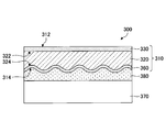
- FIG. 1 schematically shows a cross section of an image display apparatus (hereinafter, referred to as “first image display apparatus”) according to an embodiment of the present invention.
- the first image display device 100 has a cover member 110 and a display element 170.
- the cover member 110 is installed in front of the display element 170 (image display surface side). That is, the cover member 110 has an outer surface 112 and an inner surface 114, and the cover member 110 is disposed such that the inner surface 114 faces the display element 170.
- the cover member 110 has a role of protecting the display element 170.
- the outer surface 112 of the cover member 110 is a flat surface, and the inner surface 114 is an uneven surface.
- a flat surface (of the cover member 110) means a surface having an arithmetic mean roughness Ra of less than 8 nm.
- corrugated surface of the cover member 110 means the surface whose arithmetic mean roughness Ra is more than 10 nm.
- the display element 170 is configured of, for example, an element such as a liquid crystal display element, an organic EL display element, or a plasma display element capable of displaying an image on the image display surface side, that is, the cover member 110 side.
- a gap that is, an air layer S is formed between the cover member 110 and the display element 170.
- one or more transparent spacer members may be installed between the cover member 110 and the display element 170.
- the cover member 110 has a transparent substrate 120.
- the transparent substrate 120 has a first surface 122 and a second surface 124 facing each other, and the second surface 124 is disposed on the side of the display element 170.
- the cover member 110 further has a low reflective layer 130 disposed on the first surface 122 of the transparent substrate 120.
- the low reflective layer 130 has a role of suppressing reflection of external light incident from the outer surface 112 of the first image display device 100.
- the outer surface of the low reflective layer 130 constitutes the outer surface 112 of the cover member 110. Accordingly, the outer surface of the low reflective layer 130 has the aforementioned "flat surface”.
- the second surface 124 of the transparent substrate 120 constitutes the inner surface 114 of the cover member 110. Accordingly, the second surface 124 of the transparent substrate 120 has the aforementioned "concave and convex surface".
- the incident light is reflected by the effect of the low reflective layer 130 of the cover member 110. Reflection to the viewer can be significantly suppressed.
- part of the external light enters the transparent base 120 through the low reflection layer 130, such light is scattered by the inner surface 114 of the cover member 110 and hardly reflected to the viewer side Become. For this reason, the influence of light entering the inside of the first image display device 100 and reflected by the inner surface 114 of the cover member 110 is also significantly suppressed. As a result, the reflection image that may be generated due to the reflection of external light becomes unclear, and reflection of external light can be significantly suppressed.
- the outer surface 112 of the cover member 110 is a flat surface, and thus the cover member 110 has good scratch resistance.
- the first image display device 100 reflection of external light can be significantly suppressed, and the scratch resistance of the cover member 110 can be significantly improved.
- each component included in the first image display device 100 will be described in more detail.
- the referential mark shown in FIG. 1 is used.
- the transparent substrate 120 is made of, for example, a transparent material such as glass or resin. When the transparent substrate 120 is made of glass, the transparent substrate 120 may be chemically strengthened.
- the second surface 124 of the transparent substrate 120 is an uneven surface as described above.
- This textured surface may have the following shape parameters: Arithmetic average roughness Ra; 10 nm to 50 nm, preferably 13 nm to 40 nm maximum height Rz: 100 nm to 500 nm Element average length RSm of roughness curve; 9 ⁇ m to 25 ⁇ m
- Such second surface 124 may be formed, for example, by etching the surface of the transparent substrate 120.
- the first surface 122 of the transparent substrate 120 may be a flat surface.
- the first surface 122 may have an arithmetic mean roughness Ra of less than 8 nm.
- the thickness of the transparent substrate 120 is, for example, 0.5 mm to 5.0 mm.
- the low reflective layer 130 has a function of reducing the specular reflectance of external light.
- the low reflective layer 130 may be made of, for example, a multilayer film having a repeated structure of a low refractive index layer and a high refractive index layer.
- the low refractive index layer may have, for example, a refractive index of 1.1 to 1.5.
- the low refractive index layer may be made of, for example, silicon oxide (SiO 2 ).
- the high refractive index layer is, for example, selected from the group consisting of niobium oxide (Nb 2 O 5 ), titanium oxide (TiO 2 ), zirconium oxide (ZrO 2 ), silicon nitride (SiN), and tantalum oxide (Ta 2 O 5 ). It may be configured of one or more selected.
- the number of repetitions is, for example, 2 to 6.
- the outer surface of the low reflective layer 130 has a flat surface.
- the outer surface may have an arithmetic mean roughness Ra of 8 nm or less.
- the low reflective layer 130 is not an essential component. That is, when desired optical characteristics are obtained in the first image display device 100, the low reflective layer 130 may be omitted. In that case, the first surface 122 of the transparent substrate 120 may be the outer surface of the cover member 110, and thus the first surface 122 may have a flat surface.
- the thickness of the low reflective layer 130 is, for example, 200 nm to 500 nm.
- the cover member 110 may have a reflection image diffusive index value R measured from the flat outer surface 112 side of more than 0.015. In this case, reflection of external light can be further suppressed.
- the cover member 110 may have a haze ratio of less than 10% as measured from the outer surface 112 side. In this case, when the cover member 110 is disposed on the display element, the decrease in the visibility of the image can be significantly suppressed.
- the glossiness of the cover member 110 measured from the outer surface 112 may be less than 130. In this case, glare caused by the reflected image can be significantly suppressed.
- the display element 170 may have any configuration as long as an image can be displayed on the front side (the side of the cover member 110).
- the display element 170 may be, for example, a liquid crystal display element, an organic EL display element, or a plasma display element.
- FIG. 2 schematically shows a cross section of another image display device (hereinafter, referred to as “second image display device”) according to an embodiment of the present invention.
- the second image display device 200 basically has the same configuration as that of the first image display device 100 described above. That is, the second image display device 200 includes the cover member 210 and the display element 270. In addition, an air layer S is interposed between the cover member 210 and the display element 270.
- the configuration of the cover member 210 is different from the configuration of the cover member 110 of the first image display device 100. That is, the cover member 210 has the uneven layer 240 on the second surface 224 of the transparent substrate 220.
- the inner surface 214 of the cover member 210 corresponds to the outer surface of the uneven layer 240, and the uneven layer 240 thus forms the uneven surface of the cover member 210.
- the uneven layer 240 is configured such that the refractive index is close to the refractive index of the transparent substrate 220.
- the concavo-convex layer 240 may be made of silica.
- the point that the cover member 210 includes the low reflective layer 230 having a flat surface on the outer surface 212 is the same as that of the first image display device 100. Also, the first surface 222 of the transparent substrate 220 may be flat.
- the same effect as that of the first image display device 100 can be obtained.
- the low reflection layer 230 allows the incident light to reach the viewer. Reflection can be significantly suppressed.
- the outer surface 212 of the cover member 210 is a flat surface. Therefore, the scratch resistance of the cover member 210 can be significantly improved.
- each component components constituting the second image display device 200 will be described in detail. However, with regard to most of the members constituting the second image display device 200, the descriptions regarding the constituent members constituting the first image display device 100 described above can be referred to. Therefore, the uneven layer 240 will be particularly described here.
- the uneven layer 240 constitutes the inner surface 214 of the cover member 210, that is, the uneven surface. Therefore, the concavo-convex layer 240 has an arithmetic average roughness Ra of more than 10 nm.
- the uneven surface of the uneven layer 240 may have the same shape parameter as the unevenness of the transparent substrate 120.
- the uneven layer 240 is formed of, for example, a layer containing silica as a main component.
- silica as a main component.
- “having silica as a main component” means that 90% by mass or more of SiO 2 is contained.
- the thickness of the uneven layer 240 is, for example, 200 nm to 500 nm.
- the uneven layer 240 is, for example, (I) a step of preparing a coating composition (preparation step); (Ii) applying the coating composition to the second surface of the transparent substrate (application step); (Iii) a step of firing the coating composition (firing step); It is formed through Each step will be described below.
- the coating composition has at least one of silica precursor A and particles C, and solvent B, and is prepared as follows.
- silica precursor A means the substance which forms the matrix which has a silica as a main component.
- the silica precursor A is, for example, a silane compound such as alkoxysilane, and a hydrolytic condensate thereof.
- the silica precursor A preferably contains at least one of tetraalkoxysilane and its hydrolysis condensate.
- solvent B has a function of dissolving or dispersing the silica precursor A and / or a function of dispersing the particles C.
- the solvent B may have both the function of dissolving or dispersing the silica precursor A and the function of dispersing the particles C as a dispersion medium.
- the solvent B contains at least a first solvent B1 having a boiling point of 150 ° C. or less.
- the boiling point of the first solvent B1 is preferably 50 ° C to 145 ° C, and more preferably 55 ° C to 140 ° C.
- the solvent B1 may be water.
- the solvent B may further include a second solvent having a boiling point of 150 ° C. or more.
- the particles C are made of, for example, metal oxides, metals, pigments or resins.
- the metal oxide include Al 2 O 3 , SiO 2 , SnO 2 , TiO 2 , ZrO 2 , ZnO, CeO 2 , Sb-containing SnO x , Sn-containing In 2 O 3 , RuO 2 and the like.
- the particles C may be solid particles or hollow particles, or may be porous particles or the like.
- the particles C may be used alone or in combination of two or more.
- the particles C are preferably spherical, scaly, rod-like, and needle-like silica particles from the viewpoint of suppressing the increase in the refractive index of the uneven layer 240 and reducing the reflectance.
- "Square-like" means a flat shape.
- spherical silica particles or scaly silica particles are preferable.
- composition The total amount of the silica precursor A and the particles C contained in the coating composition is 30% by mass to 100% by mass of the solid content in the coating composition (however, the silica precursor A is converted to SiO 2 ) Preferably, 40% by mass to 100% by mass is more preferable. If it is this range, the uneven
- the solid content of the coating composition is represented by the sum of the contents of all the components except the solvent B in the coating composition.
- the solid content concentration of the coating composition is preferably 0.05% by mass to 2% by mass, and more preferably 0.1% by mass to 1% by mass, with respect to the total amount of the coating composition.
- the viscosity at the application temperature of the coating composition (hereinafter also referred to as “liquid viscosity”) is, for example, 0.003 Pa ⁇ S or less, and preferably 0.001 to 0.003 Pa ⁇ S.
- the viscosity of the coating composition is a value measured by a B-type viscometer.
- the coating composition described above is applied onto the second surface 224 of the transparent substrate 220.
- the method of applying the coating composition is not particularly limited.
- the coating composition may be applied on the transparent substrate 220 by, for example, a spray method or a brush coating method.
- a drying treatment may be performed after the application step.
- the coating composition is fired to form the uneven layer 240.
- the firing temperature is, for example, 100 ° C. to 750 ° C., and preferably 150 ° C. to 550 ° C.
- the uneven layer 240 can be formed on the second surface 224 of the transparent substrate 220.
- the cover member 210 may have a haze ratio of 10% or less measured from the side of the flat outer surface 212.
- the cover member 210 may have a reflection image diffusive index value R measured from the outer surface 212 side of 0.015 or more.
- the cover member 210 may have a glossiness of 130 or less measured from the side of the outer surface 212.
- FIG. 3 schematically shows a cross section of still another image display device (hereinafter, referred to as “third image display device”) according to an embodiment of the present invention.
- the third image display apparatus 300 has a cover member 310, a display element 370, and an adhesive layer 380 disposed between the two.
- the cover member 310 is installed in front of the display element 370 (image display surface side). That is, cover member 310 has an outer surface 312 and an inner surface 314, and cover member 310 is arranged such that inner surface 314 is in contact with adhesive layer 380.
- the outer surface 312 of the cover member 310 is a flat surface, and the inner surface 314 is an uneven surface.
- the display element 370 is configured of an element capable of displaying an image on the image display surface side, that is, the cover member 310 side.
- the adhesive layer 380 also has a role of bonding the cover member 310 and the display element 370.
- the cover member 310 has a transparent substrate 320.
- the transparent substrate 320 has a first surface 322 and a second surface 324 facing each other, and the second surface 324 is disposed on the side of the display element 370.
- the cover member 310 further has a low reflective layer 330 disposed on the first surface 322 of the transparent substrate 320.
- the low reflective layer 330 has a role of suppressing reflection of external light incident from the outer surface 312 of the third image display device 300.
- the low reflective layer 330 has a flat surface, and the outer surface of the low reflective layer 330 constitutes the outer surface 312 of the cover member 310.
- the second surface 324 of the transparent substrate 320 has an uneven surface
- the reflective scattering layer 360 is provided on the second surface 324. Because the reflective scattering layer 360 has a small thickness, the surface morphology of the reflective scattering layer 360 reflects the shape of the second surface 324 of the transparent substrate 320. Therefore, the surface of the reflective scattering layer 360 is an uneven surface. Also, the uneven surface of the reflective scattering layer 360 constitutes the uneven surface of the inner surface 314 of the cover member 310.
- the reflective scattering layer 360 has a role of reflecting a part of incident light to the viewing side as scattered light.
- the same effects as those of the first and second image display devices 100 and 200 described above can be obtained.
- the low reflection layer 330 allows the incident light to reach the viewer. Reflection can be significantly suppressed.
- the influence of light entering the third image display device 300 and reflected by the inner surface 314 of the cover member 310 is also significantly suppressed. As a result, reflection of external light on the cover member 310 can be significantly suppressed.
- the outer surface 312 of the cover member 310 is a flat surface, and therefore, the scratch resistance of the cover member 310 can be significantly enhanced.
- components constituting the third image display device 300 will be described in detail. However, with regard to most of the members constituting the third image display device 300, the descriptions regarding the constituent members constituting the first image display device 100 described above can be referred to. Accordingly, the reflective scattering layer 360 and the adhesive layer 380 will be described in detail here.
- the reflective scattering layer 360 constitutes the inner surface 314 of the cover member 310, that is, the uneven surface.
- the outer surface of the reflective scattering layer 360 has a maximum surface roughness Ra greater than 10 nm.
- the outer surface of the reflective scattering layer 360 may have the following shape parameters: Arithmetic average roughness Ra; 50 nm to 200 nm, preferably 80 nm to 160 nm maximum height; 500 nm to 2000 nm Element average length RSm of roughness curve; 15 ⁇ m to 50 ⁇ m
- the reflective scattering layer 360 may be formed of, for example, a multilayer film having a repeating structure of a low refractive index layer and a high refractive index layer.
- the low refractive index layer may have, for example, a refractive index of 1.1 to 1.5.
- the low refractive index layer may be made of, for example, silicon oxide (SiO 2 ).
- the high refractive index layer is, for example, selected from the group consisting of niobium oxide (Nb 2 O 5 ), titanium oxide (TiO 2 ), zirconium oxide (ZrO 2 ), silicon nitride (SiN), and tantalum oxide (Ta 2 O 5 ). It may be configured of one or more selected.
- the number of repetitions is, for example, 2 to 6.
- the thickness of the reflective scattering layer 360 is, for example, 50 nm to 200 nm.
- the adhesive layer 380 is made of, for example, a transparent resin.
- the adhesive layer 380 may be an adhesive.
- the adhesive for example, optical pressure-sensitive adhesive SK dyne (registered trademark) series (manufactured by Soken Chemical Co., Ltd.), optically transparent adhesive Locktite (registered trademark) series (manufactured by Henkel), and optical transparent adhesive sheet LUCIACS (registered Trademark CS986 series (manufactured by Nitto Denko Corporation) and the like.
- the thickness of the adhesive layer 380 is, for example, 20 ⁇ m to 500 ⁇ m.
- the adhesive layer 380 may be composed of a plurality of layers.
- the absolute value ⁇ n of the refractive index difference between the adhesive layer 380 and the transparent substrate 320 is 0 to 0.1.
- the ⁇ n is preferably 0.07 or less, more preferably 0.05 or less.
- the cover member 310 may have a haze ratio of less than 20% measured from the side of the flat outer surface 312. Further, the cover member 310 may have a reflection image diffusive index value R measured from the side of the outer surface 312 of 0.03 or more. Furthermore, the cover member 310 may have a glossiness of 85 or less as measured from the outer surface 312 side.
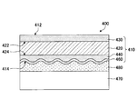
- FIG. 4 schematically shows a cross section of still another image display device (hereinafter, referred to as “fourth image display device”) according to an embodiment of the present invention.
- the fourth image display apparatus 400 basically has the same configuration as the above-described third image display apparatus 300. That is, the fourth image display device 400 includes the cover member 410 and the display element 470. Further, the cover member 410 and the display element 470 are bonded to each other by the adhesive layer 480.
- the configuration of the cover member 410 is different from the configuration of the cover member 310 of the third image display apparatus 300. That is, the cover member 410 has the uneven layer 440 on the second surface 424 of the transparent substrate 420, and the reflective scattering layer 460 is disposed on the uneven layer 440.
- the surface shape of the reflective scattering layer 460 reflects the surface shape of the uneven layer 440. Therefore, the surface of the reflective scattering layer 460 is an uneven surface. Further, the uneven surface of the reflective scattering layer 460 is the uneven surface of the inner surface 414 of the cover member 410.
- the uneven layer 440 is configured such that the refractive index approaches the refractive index of the transparent substrate 420.
- the concavo-convex layer 440 may be made of silica.
- the description of the concavo-convex layer 240 in the second image display device 200 can be referred to.
- the point that the cover member 410 includes the low reflective layer 430 having a flat surface on the outer surface 412 is the same as that of the third image display device 300.
- the first surface 422 of the transparent substrate 420 may be a flat surface.
- the same effects as those of the first image display device 100 to the third image display device 300 can be obtained.
- the low reflection layer 430 allows the incident light to reach the viewer. Reflection can be significantly suppressed. Also, even if part of the external light enters the transparent base 420 through the low reflective layer 430, such light is scattered by the inner surface 414 of the cover member 410 and is less likely to be reflected by the viewer Become. Therefore, the influence of light entering the fourth image display apparatus 400 and reflected by the inner surface 414 of the cover member 410 is also significantly suppressed. As a result, the reflection image of the external light becomes unclear, and reflection of the external light onto the cover member 410 can be significantly suppressed.
- the outer surface 412 of the cover member 410 is a flat surface, which can significantly enhance the scratch resistance of the cover member 410.
- the cover member 410 may have a haze ratio measured from the side of the flat outer surface 412 of less than 20%.
- the cover member 410 may have a reflection image diffusive index value R measured from the outer surface 412 side of 0.03 or more.
- the cover member 410 may have a glossiness of 85 or less measured from the side of the outer surface 412.
- constituent members of the first image display device 100 to the third image display device 300 can be referred to for constituent members of the fourth image display device 400. Therefore, it will not be described further here.
- Examples 1 to 14 and Examples 31 to 41 are Examples. Further, Examples 51 to 52 are comparative examples.
- Example 1 The cover member having the configuration as shown in FIG. 2 was produced by the following method.
- a soda lime glass substrate (FL 1.1; manufactured by Asahi Glass Co., Ltd.) of 100 mm long ⁇ 100 mm wide ⁇ 1 mm thick was used.
- the average transmittance of this glass substrate to light of wavelengths 400 nm to 1100 nm is 90.5%.
- the arithmetic mean roughness Ra of the first and second surfaces is 0.5 nm.
- a low reflection layer was formed on the first surface of this transparent substrate.
- the low reflective layer has a repetitive structure of a niobium oxide film (refractive index of about 2.35 at a wavelength of 632 nm) and a silicon oxide film (refractive index of about 1.47 at a wavelength of 632 nm) by post reaction sputtering.
- the film was formed.
- the number of repetitions was four, that is, four niobium oxide films and four silicon oxide films were formed.
- ULDis manufactured by ULVAC, Inc.
- a metal niobium target was used as a target for forming the niobium oxide film.
- the deposition gas was argon (40 sccm), and the sputtering power was 5 kW.
- Oxygen (100 sccm) was used as the oxidizing source gas, and the oxidizing source power was 2 kW.
- the deposition rate was 0.42 nm / min.
- polysilicon was used as a target for forming a silicon oxide film.
- the deposition gas was argon (40 sccm), and the sputtering power was 6 kW.
- Oxygen (100 sccm) was used as the oxidizing source gas, and the oxidizing source power was 1 kW.
- the deposition rate was 0.3 nm / min.
- each film is, in the order from the transparent substrate, 4.5 nm (first niobium oxide film), 61.0 nm (first silicon oxide film), 19.5 nm (second niobium oxide film), 30.0 nm (second silicon oxide film), 98.5 nm (third niobium oxide film), 16.5 nm (third silicon oxide film), 14.0 nm (fourth niobium oxide film), and 48 .0 nm (the fourth silicon oxide film).
- the low reflective layer having such a configuration is referred to as “AR1”.
- the uneven layer was formed on the second surface of the transparent substrate by the following method.
- tetraethoxysilane and KBM-3066 correspond to the silica precursor A described above.
- the SLV liquid is a dispersion obtained by crushing and dispersing scaly silica particles (Sun Green LFS HN 150; manufactured by AGC S IT Co., Ltd.), and corresponds to the particle C described above.
- the dispersion medium is water, and the concentration of particles is 5 wt%.
- the average particle size of the particles is 185 nm, and the average aspect ratio is 80.
- solution I a solution containing silica precursor A, particles C, and solvent B (hereinafter referred to as “solution I”) was obtained.
- the coating composition was spray-coated on the second surface of the transparent substrate using an electrostatic coating apparatus (a liquid electrostatic core; manufactured by Asahi Sanac Co., Ltd.) equipped with an electrostatic coating gun.
- an electrostatic coating gun a rotary atomization type automatic electrostatic gun with a cup diameter of 70 mm (San Bell, ESA 120; manufactured by Asahi Sanac Co., Ltd.) was used. The number of times of application was 3 times.
- the coating composition was baked at 300 ° C. for 1 hour to form an uneven layer on the second surface of the transparent substrate.
- cover member according to Example 1 a cover member (hereinafter, referred to as “cover member according to Example 1") was manufactured.
- the surface of the low reflection layer corresponds to the outer surface of the cover member
- the surface of the uneven layer corresponds to the inner surface of the cover member.
- Example 2 A cover member was produced in the same manner as in Example 1.
- cover members (hereinafter, referred to as “cover members according to Examples 2 to 6”) were manufactured.
- Example 7 A cover member was produced in the same manner as in Example 1.
- Example 7 the configuration (film thickness) of the low reflective layer was changed from that of Example 1.
- the low reflective layer is, in order from the transparent substrate, 7.0 nm (first niobium oxide film), 60.2 nm (first silicon oxide film), 19.0 nm (second niobium oxide film), 20.0 nm (second silicon oxide film), 94.92 nm (third niobium oxide film), 17.12 nm (third silicon oxide film), 9.32 nm (fourth niobium oxide film), and 77 .21 nm (fourth silicon oxide film).
- AR2 the low reflective layer having such a configuration is referred to as "AR2".
- cover member according to Example 7 The other manufacturing conditions are the same as in Example 1. Thereby, a cover member (hereinafter, referred to as “cover member according to Example 7") was manufactured.
- Example 8 to Example 14 A cover member was produced in the same manner as in Example 7.
- cover member (hereinafter, referred to as “cover member according to each of Examples 8 to 14”) was manufactured.
- Table 1 below collectively shows the specifications and the like of the low reflective layer and the uneven layer in the cover member according to Examples 1 to 14.
- the shape parameter of the surface of the uneven layer was measured according to the method defined in JIS B0601-2013. Specifically, the arithmetic mean roughness Ra, maximum height Rz, root mean square height Rq, element mean length RSm of roughness curve, root mean square slope R ⁇ q, skewness Rsk, and kurtosis Rku of the uneven layer are measured. did.
- the measurement was performed in the area near the center of the cover member.
- the measured value is the arithmetic mean at three points in the region.
- the scratch resistance of the outer surface (the surface on the low reflection layer side) of each cover member was evaluated.
- the scratch resistance was evaluated by pencil hardness.
- the pencil hardness was measured in accordance with JIS K5600-5-4.
- the antiglare property was evaluated using a reflection image diffuseness index value R (Reflection Image Diffusiveness index value).
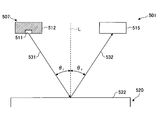
- FIG. 5A schematically shows an example of a measuring apparatus used when measuring the reflection image diffusive index value R of the cover member.
- the measuring device 501 has a linear light source device 507 and a surface luminance measuring device 515.
- the linear light source device 507 has a light source 511 and a black flat plate 512 around it.
- the light source 511 is a linear light source extending in a direction perpendicular to the paper in FIG. 5A, and is installed in a slit-like opening provided at the center of the black flat plate 512.
- the surface brightness measuring device 515 is disposed on a plane perpendicular to the longitudinal axis of the light source 511 and passing substantially through the center of the light source 511. Therefore, the surface brightness measuring device 515 is disposed to face the light source 511 at a position approximately at the center of the light source 511 along the longitudinal axis.
- the distance between the surface brightness measuring device 515 and the light source 511 is about 60 mm.
- the focus of the surface brightness measuring device 515 is focused on the image of the linear light source device 507 reflected by the outer surface 522 of the cover member 520.
- the cover member 520 to be measured is disposed in the measuring device 501 such that the outer surface 522 is on the side of the linear light source device 507 and the surface luminance measuring device 515.
- the outer surface 522 is the outer surface of the low reflection layer.
- Light emitted from the linear light source device 507 is incident on the outer surface 522 of the cover member 520 at an incident angle theta i. Further, this light is reflected and / or scattered by the outer surface 522 of the cover member 520 at the reflection angle ⁇ r , and is incident on the surface brightness measuring device 515.
- FIG. 5A shows that the first incident light 531 from the linear light source device 507 is specularly reflected on the outer surface 522 to become the first reflected light 532 and is incident on the surface luminance measuring device 515. ing.
- ⁇ r ⁇ i 0 ° holds between the incident angle ⁇ i of the first incident light 531 and the reflection angle ⁇ r of the first reflected light 532.
- the luminance of the first reflected light 532 measured by the surface luminance measuring instrument 515 is R 1 and Do.
- FIG. 5B shows how the second incident light 533 from the linear light source device 507 is scattered and reflected by the outer surface 522 to become the second reflected light 534 and is incident on the surface luminance measuring device 515. It is done.
- ⁇ r ⁇ i 0.5 ° ⁇ 0.1 ° when established, are measured in the plane luminance meter 515, the luminance of the second reflected light 534 and R 2.
- ⁇ r ⁇ i ⁇ 0.5 ° ⁇ 0.1 ° is established between the incident angle ⁇ i of the second incident light 533 and the reflection angle ⁇ r of the second reflected light 534
- the luminance of the second reflected light 534 measured by the surface luminance measuring device 515 in this case is R 3 .
- Such measurement can be performed, for example, by using an apparatus SMS-1000 manufactured by DM & S. If this device is used, a C1614A lens with a camera lens focal length of 16 mm is used with a stop 5.6. In addition, the distance from the outer surface 522 to the camera lens is about 300 mm, and the imaging scale is set in the range of 0.0276 to 0.0278.
- the dimension of the opening of the slit formed in the black flat plate 512 of the linear light source device 507 is 101 mm ⁇ 1 mm.
- the cover member to be measured is disposed on a commercially available display device (in this case, using iPad-Air (registered trademark)) via an adhesive sheet.
- an acrylic optical transparent pressure-sensitive adhesive sheet having a thickness of 500 ⁇ m was used. Further, at the time of bonding, the cover member was disposed on the display device such that the side of the second surface of the transparent substrate, that is, the side of the uneven layer faced the display device. Therefore, the cover member is disposed such that the low reflection layer side is the outer surface (viewing side).
- the display device is turned on to display a green single color image (RGB (0, 255, 0)) on the entire display screen.
- the cover members according to Examples 1 to 14 all had a flat outer surface, and the inner surface was an uneven surface.
- the reflection image diffusive index value R is 0.016 or more in all cases. From this, it was found that the cover members according to Examples 1 to 14 can significantly suppress the reflection of external light when disposed on the display element.
- Example 31 A cover member having a configuration as shown in FIG. 4 was produced by the following method.
- Example 31 the structure of a transparent base material and a low reflection layer is the same as that of the case of the above-mentioned Example 7.
- the uneven layer was formed on the second surface of the transparent substrate by the following method.
- the coating composition was spray-coated on the second surface of the transparent substrate using an electrostatic coating apparatus (a liquid electrostatic core; manufactured by Asahi Sanac Co., Ltd.) equipped with the aforementioned electrostatic coating gun. .
- the number of times of application was two.
- the coating composition was baked at 300 ° C. for 1 hour to form an uneven layer on the second surface of the transparent substrate.
- the reflective layer has a repetitive structure of a niobium oxide film (refractive index of about 2.35 at a wavelength of 632 nm) and a silicon oxide film (refractive index of about 1.47 at a wavelength of 632 nm). I made a film. The number of repetitions was 2.5, that is, three niobium oxide films and two silicon oxide films were formed.
- the film forming conditions are the same as the conditions shown in the column of (formation of low reflective layer) in Example 1.
- each film is 16.0 nm (first niobium oxide film), 34.75 nm (first silicon oxide film), 72.0 nm (second niobium oxide film) in the order from the transparent substrate, The thicknesses were 17.5 nm (second silicon oxide film) and 20.0 nm (third niobium oxide film).
- Reflect layer of the structure which concerns is called "Re1".
- cover member according to Example 31 a cover member (hereinafter, referred to as “cover member according to Example 31") was manufactured.
- the surface of the low reflective layer corresponds to the outer surface of the cover member
- the surface of the reflective layer corresponds to the inner surface of the cover member.
- Example 32 to Example 36 A cover member was produced in the same manner as in Example 31.
- Example 32 to 36 the amounts of components contained in the coating composition used in forming the uneven layer and the number of times of application by the electrostatic coating gun were changed from those in Example 31.
- cover member (hereinafter, referred to as “cover member according to each of Examples 32 to 36”) was manufactured.
- Example 37 A cover member was produced in the same manner as in Example 31.
- Example 37 the number of times of application of the coating composition was set to 3 when forming the uneven layer.
- the configuration (film thickness) of the reflective layer was changed from that of Example 31.
- the reflective layer is 16.0 nm (first niobium oxide film), 35.0 nm (first silicon oxide film), 64.0 nm (second niobium oxide film), 12 in order of increasing distance from the transparent substrate. .0 nm (second silicon oxide film) and 18.0 nm (third niobium oxide film).
- the reflective layer having such a configuration is referred to as “Re2”.
- cover member according to example 37 a cover member (hereinafter, referred to as “cover member according to example 37") was manufactured.
- Example 38 to Example 41 A cover member was produced in the same manner as in Example 37.
- cover member (hereinafter, referred to as “cover member according to each of Examples 38 to 41”) was manufactured.
- Table 3 below collectively shows the specifications of the low reflective layer, the uneven layer, the reflective layer, and the like in the cover members according to Examples 31 to 41.
- the Ra on the surface of the reflective layer is more than 10 nm.
- the surface roughness (Ra) of the surface of the low reflective layer was 8 nm or less.
- the reflection image diffusive index value R is 0.03 or more in all cases. From this, it was found that the cover members according to Examples 31 to 41 can significantly suppress the reflection of external light when disposed on the display element.
- the cover members according to Examples 31 to 41 it was found that the haze was less than 20%, and there was little possibility of lowering the visibility of the image when disposed on the display element. In addition, it was found that glare was also significantly suppressed in the cover members according to Examples 31 to 41. Further, in the cover members according to Examples 31 to 39, it was found that the glossiness was less than 85, and the glare caused by the reflected image was also significantly suppressed.
- Example 51 The cover member was produced by the following method.
- a washed transparent substrate was prepared.
- the same glass substrate (FL 1.1; manufactured by Asahi Glass Co., Ltd.) as in Example 1 was used.
- the uneven layer was formed as follows.
- a solution I was prepared by the same method as in Example 1 described above.
- the coating composition was then spray applied to the first surface of the transparent substrate using an electrostatic coating apparatus equipped with the aforementioned electrostatic coating gun.
- the number of times of application was 3 times.
- corrugated layer was formed in the 1st surface of a transparent base material by baking a coating composition at 300 degreeC for 1 hour.
- cover member according to example 51 a cover member (hereinafter, referred to as “cover member according to example 51") was manufactured.
- the surface of the uneven layer corresponds to the outer surface of the cover member
- the second surface of the transparent substrate is the surface of the cover member. Correspond to the inner surface.
- Example 52 A cover member was produced in the same manner as in Example 51.
- cover member according to example 52 a cover member (hereinafter referred to as "cover member according to example 52") was manufactured.
- Table 5 below collectively shows the specifications of the concavo-convex layers in the cover members according to Examples 51 to 52.
- the measurement of the reflective image diffusive index value R was performed such that the side of the concavo-convex layer was on the side of the linear light source device 507 and the surface luminance measuring instrument 515.
- Ra on the surface of the concavo-convex layer is more than 10 nm. It turns out that it is the surface.
- the cover members according to Example 51 to Example 52 each had a pencil hardness of only about 6 H on the outer surface. Therefore, when these cover members are arranged such that the side of the second surface of the transparent substrate faces the display element, it can be said that the outer surface does not have very good scratch resistance.
- the display device As described above, in the display device according to the embodiment of the present invention, it is possible to significantly suppress the reflection of external light, and to significantly improve the scratch resistance of the outer surface of the cover member as compared with the conventional case. confirmed.
- first image display device 110 cover member 112 outer surface (flat surface) of the cover member 114 Inner surface of cover member (rough surface) 120 Transparent substrate 122 First surface 124 Second surface 130 Low reflection layer 170 Display element 200 Second image display device 210 Cover member 212 Outer surface of cover member (flat surface) 214 Inner surface of cover member (rough surface) 220 Transparent substrate 222 First surface 224 Second surface 230 Low reflective layer 240 Irregular layer 270 Display element 300 Third image display device 310 Cover member 312 Outer surface of cover member (flat surface) 314 Inner surface of cover member (rough surface) 320 Transparent substrate 322 First surface 324 Second surface 330 Low reflective layer 360 Reflective scattering layer 370 Display element 380 Adhesive layer 400 Fourth image display device 410 Cover member 412 Outer surface of cover member (flat surface) 414 Inner surface of cover member (rough surface) 420 transparent substrate 422 first surface 424 second surface 430 low reflective layer 440 uneven layer 460 reflective scattering layer 470 display element 480 adhesive layer 501 measuring device 507 linear light
Landscapes
- Physics & Mathematics (AREA)
- General Physics & Mathematics (AREA)
- Nonlinear Science (AREA)
- Optics & Photonics (AREA)
- Crystallography & Structural Chemistry (AREA)
- Chemical & Material Sciences (AREA)
- Mathematical Physics (AREA)
- Engineering & Computer Science (AREA)
- Theoretical Computer Science (AREA)
- Devices For Indicating Variable Information By Combining Individual Elements (AREA)
- Liquid Crystal (AREA)
- Surface Treatment Of Optical Elements (AREA)
- Electroluminescent Light Sources (AREA)
- Optical Elements Other Than Lenses (AREA)
Abstract
画像表示装置であって、表示素子と、該表示素子上に設置された、透明基材を有するカバー部材と、を有し、前記カバー部材は、前記表示素子の側に、凹凸表面を有し、前記表示素子とは反対の側に、平滑な外表面を有する、画像表示装置。
Description
本発明は、画像表示装置に関する。
通常、液晶ディスプレイ、有機ELディスプレイ、およびプラズマディスプレイ等の画像表示装置は、表示素子の表示面側に、表示素子の保護のためのカバーガラスを備えている。そのような画像表示装置において、室内照明等の外部光がカバーガラスに映り込むと、表示素子から投影される画像の視認性が低下する。
そこで、そのような外部光の映り込みを抑制するため、カバーガラスの外表面には、しばしば微細な凹凸が形成される(防眩処理)。
防眩処理により、外部からカバーガラスに入射される光の反射光が散乱され、カバーガラスへの外部光の映り込みが抑制される。防眩処理としては、例えば、カバーガラスの表面をエッチングして凹凸を形成する方法、およびカバーガラスの表面に凹凸層をコーティングする方法などが知られている(例えば、特許文献1)。
前述のような外部光の映り込みをより抑制するには、カバーガラスの表面に設けられる凹凸をなるべく大きくすることが有効である。
しかしながら、そのような凹凸が大きくなればなるほど、今度はカバーガラスの表面に傷が付きやすくなり、すなわちカバーガラスの耐擦傷性が低下するという問題が生じ得る。
本発明は、このような背景に鑑みなされたものであり、本発明では、外部光の映り込みを抑制することができる上、耐擦傷性が改善された、カバー部材を有する画像表示装置を提供することを目的とする。
本発明では、
画像表示装置であって、
表示素子と、
該表示素子上に設置された、透明基材を有するカバー部材と、
を有し、
前記カバー部材は、前記表示素子の側に、凹凸表面を有し、前記表示素子とは反対の側に、平滑な外表面を有する、画像表示装置が提供される。
画像表示装置であって、
表示素子と、
該表示素子上に設置された、透明基材を有するカバー部材と、
を有し、
前記カバー部材は、前記表示素子の側に、凹凸表面を有し、前記表示素子とは反対の側に、平滑な外表面を有する、画像表示装置が提供される。
本発明では、外部光の映り込みを抑制することができる上、耐擦傷性が改善されたカバー部材を有する画像表示装置を提供することができる。
以下、図面を参照して、本発明の一実施形態について説明する。
(本発明の一実施形態による画像表示装置)
図1を参照して、本発明の一実施形態による画像表示装置について説明する。
図1を参照して、本発明の一実施形態による画像表示装置について説明する。
図1には、本発明の一実施形態による画像表示装置(以下、「第1の画像表示装置」と称する)の断面を概略的に示す。
図1に示すように、第1の画像表示装置100は、カバー部材110と、表示素子170とを有する。
カバー部材110は、表示素子170の前方(画像表示面側)に設置される。すなわち、カバー部材110は、外表面112および内表面114を有し、カバー部材110は、内表面114が表示素子170と対面するように配置される。
カバー部材110は、表示素子170を保護する役割を有する。カバー部材110の外表面112は、平坦な表面であり、内表面114は、凹凸表面である。
ここで、「(カバー部材110の)平坦な表面」とは、算術平均粗さRaが8nm未満の表面を意味する。また、「カバー部材110の」凹凸表面」とは、算術平均粗さRaが10nm超の表面を意味する。
表示素子170は、例えば、液晶表示素子、有機EL表示素子、またはプラズマ表示素子など、画像表示面側、すなわちカバー部材110側に、画像を表示できる素子で構成される。
なお、カバー部材110と表示素子170の間には、隙間、すなわち空気層Sが形成される。このため、カバー部材110と表示素子170の間には、1または2以上の透明なスペーサ部材(図示されていない)が設置されても良い。
カバー部材110は、透明基材120を有する。透明基材120は、相互に対向する第1の表面122および第2の表面124を有し、第2の表面124が表示素子170の側となるように配置される。
カバー部材110は、さらに、透明基材120の第1の表面122に設置された、低反射層130を有する。低反射層130は、第1の画像表示装置100の外表面112から入射される外光の反射を抑制する役割を有する。
低反射層130の外表面は、カバー部材110の外表面112を構成する。従って、低反射層130の外表面は、前述の「平坦な表面」を有する。
一方、透明基材120の第2の表面124は、カバー部材110の内表面114を構成する。従って、透明基材120の第2の表面124は、前述の「凹凸表面」を有する。
このような構成の第1の画像表示装置100では、カバー部材110の低反射層130の効果により、第1の画像表示装置100に外部から光(外部光)が入射しても、入射光が観者の方に反射されることを有意に抑制することができる。また、外部光の一部が低反射層130を介して透明基材120まで入射しても、そのような光は、カバー部材110の内表面114で散乱され、観者側には反射されにくくなる。このため、第1の画像表示装置100の内部に進入し、カバー部材110の内表面114で反射される光による影響も、有意に抑制される。その結果、外部光の反射によって生じ得る反射像が不鮮明になり、外部光の映り込みを有意に抑制することが可能になる。
また、第1の画像表示装置100では、カバー部材110の外表面112が、平坦な表面となっており、このため、カバー部材110は、良好な耐擦傷性を有する。
従って、第1の画像表示装置100では、外部光の映り込みを有意に抑制することができるとともに、カバー部材110の耐擦傷性を有意に高めることができる。
(各構成部材)
次に、第1の画像表示装置100に含まれる各構成部材について、より詳しく説明する。なお、各構成部材を表す際には、図1に示した参照符号を使用する。
次に、第1の画像表示装置100に含まれる各構成部材について、より詳しく説明する。なお、各構成部材を表す際には、図1に示した参照符号を使用する。
(透明基材120)
透明基材120は、例えば、ガラスまたは樹脂などの透明な材料で構成される。透明基材120がガラスで構成される場合、透明基材120は化学強化されていても良い。
透明基材120は、例えば、ガラスまたは樹脂などの透明な材料で構成される。透明基材120がガラスで構成される場合、透明基材120は化学強化されていても良い。
透明基材120の第2の表面124は、前述のように、凹凸表面である。
この凹凸表面は、以下のような形状パラメータを有しても良い:
算術平均粗さRa;10nm~50nmであり、13nm~40nmが好ましい
最大高さRz;100nm~500nm
粗さ曲線の要素平均長さRSm;9μm~25μm
そのような第2の表面124は、例えば、透明基材120の表面をエッチングすることにより、形成されても良い。
算術平均粗さRa;10nm~50nmであり、13nm~40nmが好ましい
最大高さRz;100nm~500nm
粗さ曲線の要素平均長さRSm;9μm~25μm
そのような第2の表面124は、例えば、透明基材120の表面をエッチングすることにより、形成されても良い。
一方、透明基材120の第1の表面122は、平坦な表面であっても良い。例えば、第1の表面122は、算術平均粗さRaが8nm未満であっても良い。
透明基材120の厚さは、例えば、0.5mm~5.0mmである。
(低反射層130)
低反射層130は、外部光の正反射率を低下させる機能を有する。
低反射層130は、外部光の正反射率を低下させる機能を有する。
低反射層130は、例えば、低屈折率層と高屈折率層の繰り返し構造を有する多層膜で構成されても良い。
低屈折率層は、例えば、1.1~1.5の屈折率を有しても良い。低屈折率層は、例えば、酸化ケイ素(SiO2)で構成されても良い。
高屈折率層は、例えば、酸化ニオブ(Nb2O5)、酸化チタン(TiO2)、酸化ジルコニウム(ZrO2)、窒化ケイ素(SiN)、および酸化タンタル(Ta2O5)からなる群から選択された1種以上で構成されても良い。
なお、繰り返し数は、例えば2~6である。
低反射層130の外表面は、平坦な表面を有する。外表面は、算術平均粗さRaが8nm以下であっても良い。
なお、低反射層130は、必須の構成ではない。すなわち、第1の画像表示装置100に所望の光学特性が得られる場合、低反射層130は省略しても良い。その場合、透明基材120の第1の表面122がカバー部材110の外表面となり、従って、第1の表面122が平坦な表面を有しても良い。
低反射層130の厚さは、例えば、200nm~500nmである。
(カバー部材110)
カバー部材110は、平坦な外表面112の側から測定される反射像拡散性指標値Rが0.015超であっても良い。この場合、外光の映り込みをよりいっそう抑制することができる。
カバー部材110は、平坦な外表面112の側から測定される反射像拡散性指標値Rが0.015超であっても良い。この場合、外光の映り込みをよりいっそう抑制することができる。
また、カバー部材110は、外表面112の側から測定されるヘイズ率が10%未満であっても良い。この場合、表示素子の上にカバー部材110を配置した際に、画像の視認性の低下を、有意に抑制することができる。
また、カバー部材110は、外表面112の側から測定される光沢度が130未満であっても良い。この場合、反射像による眩しさを、有意に抑制することができる。
なお、これらの光学パラメータの測定方法については、後述する。
(表示素子170)
表示素子170は、前方(カバー部材110の側)に画像を表示することができる限り、いかなる構成を有しても良い。表示素子170は、例えば、液晶表示素子、有機EL表示素子、またはプラズマ表示素子であっても良い。
表示素子170は、前方(カバー部材110の側)に画像を表示することができる限り、いかなる構成を有しても良い。表示素子170は、例えば、液晶表示素子、有機EL表示素子、またはプラズマ表示素子であっても良い。
(本発明の一実施形態による別の画像表示装置)
次に、図2を参照して、本発明の一実施形態による別の画像表示装置について説明する。
次に、図2を参照して、本発明の一実施形態による別の画像表示装置について説明する。
図2には、本発明の一実施形態による別の画像表示装置(以下、「第2の画像表示装置」と称する)の断面を概略的に示す。
図2に示すように、第2の画像表示装置200は、基本的に、前述の第1の画像表示装置100と同様の構成を有する。すなわち、第2の画像表示装置200は、カバー部材210と、表示素子270とを有する。また、カバー部材210と表示素子270の間には、空気層Sが介在される。
ただし、第2の画像表示装置200においては、カバー部材210の構成が、第1の画像表示装置100のカバー部材110の構成とは異なっている。すなわち、カバー部材210は、透明基材220の第2の表面224に、凹凸層240を有する。
換言すれば、カバー部材210の内表面214は、凹凸層240の外表面に対応し、従って、凹凸層240によって、カバー部材210の凹凸面が形成される。
凹凸層240は、屈折率が透明基材220の屈折率と接近するように構成される。例えば、透明基材220がガラスで構成される場合、凹凸層240は、シリカで構成されても良い。
なお、カバー部材210が外表面212に、平坦な表面を有する低反射層230を備える点は、第1の画像表示装置100の場合と同様である。また、透明基材220の第1の表面222は、平坦であっても良い。
このような構成を有する第2の画像表示装置200においても、第1の画像表示装置100と同様の効果を得ることができる。
すなわち、第2の画像表示装置200では、第2の画像表示装置200のカバー部材210に外部から光(外部光)が入射しても、低反射層230によって、入射光が観者の方に反射されることを有意に抑制することができる。
また、外部光の一部が低反射層230を介して透明基材220まで入射しても、そのような光は、カバー部材210の内表面214(凹凸層240)で散乱され、観者側には反射されにくくなる。このため、第2の画像表示装置200の内部に進入し、カバー部材210の内表面214で反射される光による影響も、有意に抑制される。その結果、カバー部材210への外部光の映り込みを有意に抑制することが可能になる。
また、第2の画像表示装置200では、カバー部材210の外表面212が、平坦な表面となっている。このため、カバー部材210の耐擦傷性を有意に高めることができる。
(各構成部材)
次に、第2の画像表示装置200を構成する構成部材について、詳しく説明する。ただし、第2の画像表示装置200を構成する大部分の部材については、前述の第1の画像表示装置100を構成する構成部材に関する記載が参照できる。従って、ここでは、特に凹凸層240について説明する。
次に、第2の画像表示装置200を構成する構成部材について、詳しく説明する。ただし、第2の画像表示装置200を構成する大部分の部材については、前述の第1の画像表示装置100を構成する構成部材に関する記載が参照できる。従って、ここでは、特に凹凸層240について説明する。
(凹凸層240)
凹凸層240は、カバー部材210の内表面214、すなわち凹凸表面を構成する。従って、凹凸層240は、算術平均粗さRaが10nm超である。
凹凸層240は、カバー部材210の内表面214、すなわち凹凸表面を構成する。従って、凹凸層240は、算術平均粗さRaが10nm超である。
また、凹凸層240の凹凸表面は、透明基材120の凹凸と同様の形状パラメータを有しても良い。
凹凸層240は、例えば、シリカを主成分とする層で構成される。ここで、「シリカを主成分とする」とは、SiO2を90質量%以上含むことを意味する。
凹凸層240の厚さは、例えば、200nm~500nmである。
(凹凸層240の形成方法)
次に、凹凸層240の形成方法の一例について説明する。
次に、凹凸層240の形成方法の一例について説明する。
凹凸層240は、例えば、
(i)塗布組成物を調製する工程(調製工程)と、
(ii)前記塗布組成物を透明基材の第2の表面に塗布する工程(塗布工程)と、
(iii)前記塗布組成物を焼成する工程(焼成工程)と、
を経て形成される。以下、各工程について説明する。
(i)塗布組成物を調製する工程(調製工程)と、
(ii)前記塗布組成物を透明基材の第2の表面に塗布する工程(塗布工程)と、
(iii)前記塗布組成物を焼成する工程(焼成工程)と、
を経て形成される。以下、各工程について説明する。
(調製工程)
まず、塗布組成物が調整される。塗布組成物は、シリカ前駆体Aおよび粒子Cの少なくとも一方と、溶媒Bとを有し、以下のように調製される。なお、「シリカ前駆体A」とは、シリカを主成分とするマトリクスを形成する物質を意味する。
まず、塗布組成物が調整される。塗布組成物は、シリカ前駆体Aおよび粒子Cの少なくとも一方と、溶媒Bとを有し、以下のように調製される。なお、「シリカ前駆体A」とは、シリカを主成分とするマトリクスを形成する物質を意味する。
以下、それぞれについて説明する。
(シリカ前駆体A)
シリカ前駆体Aは、例えば、アルコキシシラン等のシラン化合物、およびその加水分解縮合物である。シリカ前駆体Aは、テトラアルコキシシランおよびその加水分解縮合物の少なくとも一方を含むことが好ましい。
シリカ前駆体Aは、例えば、アルコキシシラン等のシラン化合物、およびその加水分解縮合物である。シリカ前駆体Aは、テトラアルコキシシランおよびその加水分解縮合物の少なくとも一方を含むことが好ましい。
(溶媒B)
溶媒Bは、シリカ前駆体Aを溶解または分散する機能、および/または粒子Cを分散する機能を有する。溶媒Bは、シリカ前駆体Aを溶解または分散する機能と、粒子Cを分散する分散媒としての機能の両方を有しても良い。
溶媒Bは、シリカ前駆体Aを溶解または分散する機能、および/または粒子Cを分散する機能を有する。溶媒Bは、シリカ前駆体Aを溶解または分散する機能と、粒子Cを分散する分散媒としての機能の両方を有しても良い。
溶媒Bは、少なくとも、沸点が150℃以下の第1の溶媒B1を含む。第1の溶媒B1の沸点は、50℃~145℃が好ましく、55℃~140℃がより好ましい。溶媒B1は、水であっても良い。
溶媒Bは、さらに、沸点が150℃超の第2の溶媒を含んでも良い。
(粒子C)
粒子Cは、例えば、金属酸化物、金属、顔料または樹脂などで構成される。金属酸化物としては、Al2O3、SiO2、SnO2、TiO2、ZrO2、ZnO、CeO2、Sb含有SnOx、Sn含有In2O3、RuO2等が挙げられる。
粒子Cは、例えば、金属酸化物、金属、顔料または樹脂などで構成される。金属酸化物としては、Al2O3、SiO2、SnO2、TiO2、ZrO2、ZnO、CeO2、Sb含有SnOx、Sn含有In2O3、RuO2等が挙げられる。
粒子Cは、中実粒子でも中空粒子でも良く、多孔質粒子等でも良い。粒子Cは、1種を単独で用いても、2種以上を併用しても良い。
粒子Cとしては、凹凸層240の屈折率上昇を抑え、反射率を下げることができる点から、球状、鱗片状、棒状、および針状等のシリカ粒子が好ましい。「鱗片状」とは、扁平な形状を意味する。特に、粒子Cとしては、球状シリカ粒子または鱗片状シリカ粒子が好ましい。
(組成)
塗布組成物に含まれるシリカ前駆体Aと粒子Cの合計量は、塗布組成物中の固形分(ただし、シリカ前駆体AはSiO2換算とする)のうち、30質量%~100質量%が好ましく、40質量%~100質量%がより好ましい。この範囲であれば、透明基材220との密着性に優れる凹凸層240を形成できる。
塗布組成物に含まれるシリカ前駆体Aと粒子Cの合計量は、塗布組成物中の固形分(ただし、シリカ前駆体AはSiO2換算とする)のうち、30質量%~100質量%が好ましく、40質量%~100質量%がより好ましい。この範囲であれば、透明基材220との密着性に優れる凹凸層240を形成できる。
塗布組成物の固形分は、塗布組成物中の、溶媒Bを除く全成分の含有量の合計で表される。
塗布組成物の固形分濃度は、塗布組成物の全量に対し、0.05質量%~2質量%が好ましく、0.1質量%~1質量%がより好ましい。
塗布組成物の塗布温度における粘度(以下、「液粘度」ともいう)は、例えば、0.003Pa・S以下であり、0.001~0.003Pa・Sであることが好ましい。塗布組成物の粘度は、B型粘度計により測定される値である。
(塗布工程)
次に、前述の塗布組成物が、透明基材220の第2の表面224上に塗布される。塗布組成物の塗布の方法は、特に限られない。塗布組成物は、例えば、スプレー法、または刷毛塗り法などにより、透明基材220上に塗布されても良い。
次に、前述の塗布組成物が、透明基材220の第2の表面224上に塗布される。塗布組成物の塗布の方法は、特に限られない。塗布組成物は、例えば、スプレー法、または刷毛塗り法などにより、透明基材220上に塗布されても良い。
必要な場合、塗布工程の後に、乾燥処理を行っても良い。
(焼成工程)
次に、塗布組成物が焼成され、これにより、凹凸層240が形成される。焼成温度は、例えば、100℃~750℃であり、150℃~550℃であることが好ましい。
次に、塗布組成物が焼成され、これにより、凹凸層240が形成される。焼成温度は、例えば、100℃~750℃であり、150℃~550℃であることが好ましい。
以上の工程により、透明基材220の第2の表面224に、凹凸層240を形成することができる。
(カバー部材210)
第2の画像表示装置200において、カバー部材210は、平坦な外表面212の側から測定されるヘイズ率が10%以下であっても良い。また、カバー部材210は、外表面212の側から測定される反射像拡散性指標値Rが0.015以上であっても良い。さらに、カバー部材210は、外表面212の側から測定される光沢度が130以下であっても良い。
第2の画像表示装置200において、カバー部材210は、平坦な外表面212の側から測定されるヘイズ率が10%以下であっても良い。また、カバー部材210は、外表面212の側から測定される反射像拡散性指標値Rが0.015以上であっても良い。さらに、カバー部材210は、外表面212の側から測定される光沢度が130以下であっても良い。
(本発明の一実施形態によるさらに別の画像表示装置)
次に、図3を参照して、本発明の一実施形態によるさらに別の画像表示装置について説明する。
次に、図3を参照して、本発明の一実施形態によるさらに別の画像表示装置について説明する。
図3には、本発明の一実施形態によるさらに別の画像表示装置(以下、「第3の画像表示装置」と称する)の断面を概略的に示す。
図3に示すように、第3の画像表示装置300は、カバー部材310と、表示素子370と、両者の間に設置された接着層380とを有する。
カバー部材310は、表示素子370の前方(画像表示面側)に設置される。すなわち、カバー部材310は、外表面312および内表面314を有し、カバー部材310は、内表面314が接着層380と接触するように配置される。
カバー部材310の外表面312は、平坦な表面であり、内表面314は、凹凸表面である。
表示素子370は、前述のように、画像表示面側、すなわちカバー部材310側に、画像を表示できる素子で構成される。
また、接着層380は、カバー部材310と表示素子370とを接合する役割を有する。
カバー部材310は、透明基材320を有する。透明基材320は、相互に対向する第1の表面322および第2の表面324を有し、第2の表面324が表示素子370の側となるように配置される。
カバー部材310は、さらに、透明基材320の第1の表面322に設置された、低反射層330を有する。低反射層330は、第3の画像表示装置300の外表面312から入射される外部光の反射を抑制する役割を有する。
低反射層330は、平坦な表面を有し、低反射層330の外表面がカバー部材310の外表面312を構成する。
一方、透明基材320の第2の表面324は、凹凸表面を有し、この第2の表面324には、反射散乱層360が設置される。反射散乱層360は、厚さが薄いため、反射散乱層360の表面形態には、透明基材320の第2の表面324の形状が反映される。従って、反射散乱層360の表面は、凹凸表面である。また、反射散乱層360の凹凸表面が、カバー部材310の内表面314の凹凸表面を構成する。
反射散乱層360は、入射光の一部を視認側に散乱光として反射する役割を有する。
このような構成を有する第3の画像表示装置300においても、前述の第1および第2の画像表示装置100、200と同様の効果を得ることができる。
すなわち、第3の画像表示装置300では、第3の画像表示装置300のカバー部材310に外部から光(外部光)が入射しても、低反射層330によって、入射光が観者の方に反射されることを有意に抑制することができる。
また、外部光の一部が低反射層330を介して透明基材320まで入射しても、そのような光は、カバー部材310の内表面314で散乱され、観者側には反射されにくくなる。このため、第3の画像表示装置300の内部に進入し、カバー部材310の内表面314で反射される光による影響も、有意に抑制される。その結果、カバー部材310への外部光の映り込みを有意に抑制することが可能になる。
また、外部光の一部が低反射層330を介して透明基材320まで入射しても、そのような光は、カバー部材310の内表面314で散乱され、観者側には反射されにくくなる。このため、第3の画像表示装置300の内部に進入し、カバー部材310の内表面314で反射される光による影響も、有意に抑制される。その結果、カバー部材310への外部光の映り込みを有意に抑制することが可能になる。
また、第3の画像表示装置300では、カバー部材310の外表面312が、平坦な表面となっており、このため、カバー部材310の耐擦傷性を有意に高めることができる。
(第3の画像表示装置の構成部材)
次に、第3の画像表示装置300を構成する構成部材について、詳しく説明する。ただし、第3の画像表示装置300を構成する大部分の部材については、前述の第1の画像表示装置100を構成する構成部材に関する記載が参照できる。従って、ここでは、反射散乱層360および接着層380について詳しく説明する。
次に、第3の画像表示装置300を構成する構成部材について、詳しく説明する。ただし、第3の画像表示装置300を構成する大部分の部材については、前述の第1の画像表示装置100を構成する構成部材に関する記載が参照できる。従って、ここでは、反射散乱層360および接着層380について詳しく説明する。
(反射散乱層360)
反射散乱層360は、カバー部材310の内表面314、すなわち凹凸表面を構成する。
反射散乱層360は、カバー部材310の内表面314、すなわち凹凸表面を構成する。
従って、反射散乱層360の外表面は、10nm超の最大表面粗さRaを有する。
反射散乱層360の外表面は、以下のような形状パラメータを有しても良い:
算術平均粗さRa;50nm~200nmであり、80nm~160nmが好ましい
最大高さ;500nm~2000nm
粗さ曲線の要素平均長さRSm;15μm~50μm
反射散乱層360は、例えば、低屈折率層と高屈折率層の繰り返し構造を有する多層膜で構成されても良い。
算術平均粗さRa;50nm~200nmであり、80nm~160nmが好ましい
最大高さ;500nm~2000nm
粗さ曲線の要素平均長さRSm;15μm~50μm
反射散乱層360は、例えば、低屈折率層と高屈折率層の繰り返し構造を有する多層膜で構成されても良い。
低屈折率層は、例えば、1.1~1.5の屈折率を有しても良い。低屈折率層は、例えば、酸化ケイ素(SiO2)で構成されても良い。
高屈折率層は、例えば、酸化ニオブ(Nb2O5)、酸化チタン(TiO2)、酸化ジルコニウム(ZrO2)、窒化ケイ素(SiN)、および酸化タンタル(Ta2O5)からなる群から選択された1種以上で構成されても良い。
なお、繰り返し数は、例えば2~6である。
反射散乱層360の厚さは、例えば、50nm~200nmである。
(接着層380)
接着層380は、例えば、透明な樹脂で構成される。
接着層380は、例えば、透明な樹脂で構成される。
接着層380は、接着剤であっても良い。接着剤としては、例えば、光学用粘着剤SKダイン(登録商標)シリーズ(綜研化学社製)、光学透明接着剤ロックタイト(登録商標)シリーズ(Henkel社製)、および光学用透明粘着シートLUCIACS(登録商標)CS986シリーズ(日東電工株式会社製)などが挙げられる。
接着層380の厚さは、例えば、20μm~500μmである。
なお、接着層380は、複数の層で構成されても良い。
接着層380と透明基材320の間の屈折率差の絶対値Δnは、0~0.1である。このような構成とすることにより、透明基材320と反射散乱層360との界面、および反射散乱層360と接着層380との界面における屈折角度の差異が抑制され、視認性の低下を有意に抑制することができる。
Δnは、0.07以下であることが好ましく、0.05以下であることがより好ましい。
(カバー部材310)
カバー部材310は、平坦な外表面312の側から測定されるヘイズ率が20%未満であっても良い。また、カバー部材310は、外表面312の側から測定される反射像拡散性指標値Rが0.03以上であっても良い。さらに、カバー部材310は、外表面312の側から測定される光沢度が85以下であっても良い。
カバー部材310は、平坦な外表面312の側から測定されるヘイズ率が20%未満であっても良い。また、カバー部材310は、外表面312の側から測定される反射像拡散性指標値Rが0.03以上であっても良い。さらに、カバー部材310は、外表面312の側から測定される光沢度が85以下であっても良い。
(本発明の一実施形態によるさらに別の画像表示装置)
次に、図4を参照して、本発明の一実施形態によるさらに別の画像表示装置について説明する。
次に、図4を参照して、本発明の一実施形態によるさらに別の画像表示装置について説明する。
図4には、本発明の一実施形態によるさらに別の画像表示装置(以下、「第4の画像表示装置」と称する)の断面を概略的に示す。
図4に示すように、第4の画像表示装置400は、基本的に、前述の第3の画像表示装置300と同様の構成を有する。すなわち、第4の画像表示装置400は、カバー部材410と、表示素子470とを有する。また、カバー部材410と表示素子470は、接着層480により、相互に接合される。
ただし、第4の画像表示装置400においては、カバー部材410の構成が、第3の画像表示装置300のカバー部材310の構成とは異なっている。すなわち、カバー部材410は、透明基材420の第2の表面424に、凹凸層440を有し、反射散乱層460は、この凹凸層440の上に配置される。
前述のように、反射散乱層460は、厚さが薄いため、反射散乱層460の表面形態には、凹凸層440の表面形状が反映される。従って、反射散乱層460の表面は、凹凸表面である。また、反射散乱層460の凹凸表面が、カバー部材410の内表面414の凹凸表面となる。
凹凸層440は、屈折率が透明基材420の屈折率と接近するように構成される。例えば、透明基材420がガラスで構成される場合、凹凸層440は、シリカで構成されても良い。なお、凹凸層440の詳細については、前述の第2の画像表示装置200における凹凸層240に関する説明が参照できる。
また、カバー部材410が外表面412に、平坦な表面を有する低反射層430を備える点は、第3の画像表示装置300の場合と同様である。また、透明基材420の第1の表面422は、平坦な表面であっても良い。
このような構成を有する第4の画像表示装置400においても、第1の画像表示装置100~第3の画像表示装置300と同様の効果を得ることができる。
すなわち、第4の画像表示装置400では、第4の画像表示装置400のカバー部材410に外部から光(外部光)が入射しても、低反射層430によって、入射光が観者の方に反射されることを有意に抑制することができる。また、外部光の一部が低反射層430を介して透明基材420まで入射しても、そのような光は、カバー部材410の内表面414で散乱され、観者側には反射されにくくなる。このため、第4の画像表示装置400の内部に進入し、カバー部材410の内表面414で反射される光による影響も、有意に抑制される。その結果、外部光の反射像が不鮮明になり、カバー部材410への外光の映り込みを有意に抑制することが可能になる。
また、第4の画像表示装置400では、カバー部材410の外表面412が、平坦な表面となっており、このため、カバー部材410の耐擦傷性を有意に高めることができる。
第4の画像表示装置400において、カバー部材410は、平坦な外表面412の側から測定されるヘイズ率が20%未満であっても良い。また、カバー部材410は、外表面412の側から測定される反射像拡散性指標値Rが0.03以上であっても良い。また、カバー部材410は、外表面412の側から測定される光沢度が、85以下であっても良い。
なお、第4の画像表示装置400を構成する構成部材については、前述の第1の画像表示装置100~第3の画像表示装置300の構成部材に関する記載が参照できる。従って、ここでは、これ以上説明しない。
以上、第1の画像表示装置100~第4の画像表示装置400を参照して、本発明の一実施形態について説明した。しかしながら、これらは単なる一例であって、本発明がこれらの実施例に限られないことは、当業者には明らかである。
以下、本発明の実施例について説明する。なお、以下の説明において、例1~例14、および例31~例41は、実施例である。また、例51~例52は、比較例である。
(例1)
以下の方法により、前述の図2に示したような構成のカバー部材を作製した。
以下の方法により、前述の図2に示したような構成のカバー部材を作製した。
(低反射層の形成)
まず、洗浄された透明基材を準備した。
まず、洗浄された透明基材を準備した。
透明基材には、縦100mm×横100mm×厚さ1mmのソーダライム製のガラス基板(FL1.1;旭硝子社製)を使用した。このガラス基板の波長400nm~1100nmの光に対する平均透過率は、90.5%である。また、第1および第2の表面の算術平均粗さRaは、いずれも0.5nmである。
この透明基材の第1の表面に、低反射層を形成した。
低反射層は、酸化ニオブ膜(波長632nmにおける屈折率は、約2.35)と酸化ケイ素膜(波長632nmにおける屈折率は、屈折率約1.47)の繰り返し構造とし、後反応スパッタ法により成膜した。繰り返し数は4とし、すなわち、酸化ニオブ膜と酸化ケイ素膜とをそれぞれ、4層ずつ成膜した。
後反応スパッタ装置には、ULDis(アルバック社製)を使用した。酸化ニオブ膜の成膜の際のターゲットには、メタルニオブターゲットを使用した。成膜ガスはアルゴン(40sccm)とし、スパッタ電力は5kWとした。酸化源ガスには酸素(100sccm)を使用し、酸化源電力は2kWとした。成膜速度は、0.42nm/分とした。
一方、酸化ケイ素膜の成膜の際のターゲットには、ポリシリコンを使用した。成膜ガスはアルゴン(40sccm)とし、スパッタ電力6kWとした。酸化源ガスには酸素(100sccm)を使用し、酸化源電力は1kWとした。成膜速度は、0.3nm/分とした。
各膜の厚さは、透明基材から近い順に、4.5nm(第1の酸化ニオブ膜)、61.0nm(第1の酸化ケイ素膜)、19.5nm(第2の酸化ニオブ膜)、30.0nm(第2の酸化ケイ素膜)、98.5nm(第3の酸化ニオブ膜)、16.5nm(第3の酸化ケイ素膜)、14.0nm(第4の酸化ニオブ膜)、および48.0nm(第4の酸化ケイ素膜)とした。以下、係る構成の低反射層を、「AR1」と称する。
(凹凸層の形成)
次に、透明基材の第2の表面に、以下の方法で、凹凸層を形成した。
次に、透明基材の第2の表面に、以下の方法で、凹凸層を形成した。
(塗布組成物の調製)
25℃において、150.7gのソルミックスAP-11(日本アルコール販売社製)を撹拌しながら、19gのテトラエトキシシラン、1.1gのKBM-3066(信越化学社製)、6.2gのSLV液、および21.8gの水を添加した。
25℃において、150.7gのソルミックスAP-11(日本アルコール販売社製)を撹拌しながら、19gのテトラエトキシシラン、1.1gのKBM-3066(信越化学社製)、6.2gのSLV液、および21.8gの水を添加した。
このうち、テトラエトキシシランおよびKBM-3066(アルコキシシラン)は、前述のシリカ前駆体Aに相当する。また、SLV液は、鱗片状シリカ粒子(サンラブリーLFS HN150;AGCエスアイテック社製)を解砕、分散させた分散液であり、前述の粒子Cに対応する。分散媒は水であり、粒子の濃度は、5wt%である。また、粒子の平均粒子径は、185nmであり、平均アスペクト比は80である。
この混合液に、10質量%の硝酸水溶液を1.1g添加し、60℃で60分間混合した。
これにより、シリカ前駆体A、粒子C、および溶媒Bを含む溶液(以下、「溶液I」と称する)が得られた。
次に、27.7gの溶液Iに、372.3gのAP-11を加え、十分に撹拌した。これにより、凹凸層形成用の塗布組成物を得た。
(塗布組成物の塗布)
次に、静電塗装ガンを備える静電塗装装置(液体静電コ一夕ー;旭サナック社製)を用いて、透明基材の第2の表面に、塗布組成物をスプレー塗布した。静電塗装ガンには、カップ径が70mmの回転霧化式自動静電ガン(サンベル、ESA120;旭サナック社製)を使用した。塗布の回数は、3回とした。
次に、静電塗装ガンを備える静電塗装装置(液体静電コ一夕ー;旭サナック社製)を用いて、透明基材の第2の表面に、塗布組成物をスプレー塗布した。静電塗装ガンには、カップ径が70mmの回転霧化式自動静電ガン(サンベル、ESA120;旭サナック社製)を使用した。塗布の回数は、3回とした。
その後、塗布組成物を300℃で1時間焼成することにより、透明基材の第2の表面に凹凸層が形成された。
以上の方法により、カバー部材(以下、「例1に係るカバー部材」と称する)が製造された。なお、例1に係るカバー部材において、低反射層の表面は、カバー部材の外表面に対応し、凹凸層の表面は、カバー部材の内表面に対応する。
(例2~例6)
例1と同様の方法により、カバー部材を作製した。
例1と同様の方法により、カバー部材を作製した。
ただし、これらの例2~例6では、凹凸層を形成する際に使用する塗布組成物に含まれる成分量、および静電塗装ガンによる塗布の回数を、例1の場合とは変化させた。
これにより、カバー部材(以下、それぞれ、「例2~例6に係るカバー部材」と称する)が製造された。
(例7)
例1と同様の方法により、カバー部材を作製した。
例1と同様の方法により、カバー部材を作製した。
ただし、この例7では、低反射層の構成(膜厚)を、例1の場合とは変化させた。
すなわち、低反射層は、透明基材から近い順に、7.0nm(第1の酸化ニオブ膜)、60.2nm(第1の酸化ケイ素膜)、19.0nm(第2の酸化ニオブ膜)、20.0nm(第2の酸化ケイ素膜)、94.92nm(第3の酸化ニオブ膜)、17.12nm(第3の酸化ケイ素膜)、9.32nm(第4の酸化ニオブ膜)、および77.21nm(第4の酸化ケイ素膜)とした。以下、係る構成の低反射層を、「AR2」と称する。
その他の製造条件は、例1の場合と同様である。これにより、カバー部材(以下、「例7に係るカバー部材」と称する)が製造された。
(例8~例14)
例7と同様の方法により、カバー部材を作製した。
例7と同様の方法により、カバー部材を作製した。
ただし、これらの例8~例14では、凹凸層を形成する際に使用する塗布組成物に含まれる成分量、および静電塗装ガンによる塗布の回数を、例7の場合とは変化させた。
これにより、カバー部材(以下、それぞれ、「例8~例14に係るカバー部材」と称する)が製造された。
以下の表1には、例1~例14に係るカバー部材における低反射層および凹凸層の仕様などを、まとめて示した。

例1~例14に係るカバー部材を用いて、以下の評価を実施した。
(表面形状の評価)
各カバー部材において、凹凸層の表面の形状パラメータは、JIS B0601-2013に規定されている方法に従って測定した。具体的には、凹凸層の算術平均粗さRa、最大高さRz、二乗平均平方根高さRq、粗さ曲線の要素平均長さRSm、二乗平均平方根傾斜RΔq、スキューネスRsk、およびクルトシスRkuを測定した。
各カバー部材において、凹凸層の表面の形状パラメータは、JIS B0601-2013に規定されている方法に従って測定した。具体的には、凹凸層の算術平均粗さRa、最大高さRz、二乗平均平方根高さRq、粗さ曲線の要素平均長さRSm、二乗平均平方根傾斜RΔq、スキューネスRsk、およびクルトシスRkuを測定した。
測定は、カバー部材の中央近傍領域で実施した。測定値は、その領域の3点での算術平均である。
(耐擦傷性の評価)
各カバー部材において、外表面(低反射層側の表面)の耐擦傷性を評価した。耐擦傷性は、鉛筆硬度で評価した。鉛筆硬度は、JIS K5600-5-4に準拠して測定した。
各カバー部材において、外表面(低反射層側の表面)の耐擦傷性を評価した。耐擦傷性は、鉛筆硬度で評価した。鉛筆硬度は、JIS K5600-5-4に準拠して測定した。
(光学特性の評価)
各カバー部材を用いて、以下の光学特性を評価した。
各カバー部材を用いて、以下の光学特性を評価した。
(ヘイズ率)
ヘイズ率は、低反射層の側から、JIS K7136:2000(ISO14782:1999)に準拠した方法により測定した。
ヘイズ率は、低反射層の側から、JIS K7136:2000(ISO14782:1999)に準拠した方法により測定した。
(光沢度)
光沢度は、低反射層の側から、JIS Z8741:1997(ISO2813:1994)に記載の60°鏡面光沢度の評価方法に従って測定した。
光沢度は、低反射層の側から、JIS Z8741:1997(ISO2813:1994)に記載の60°鏡面光沢度の評価方法に従って測定した。
(防眩性)
防眩性は、反射像拡散性指標値R(Reflection Image Diffusiveness index value)を用いて評価した。
防眩性は、反射像拡散性指標値R(Reflection Image Diffusiveness index value)を用いて評価した。
以下、図5Aおよび図5Bを参照して、反射像拡散性指標値Rの測定方法について説明する。
図5Aには、カバー部材の反射像拡散性指標値Rを測定する際に使用される測定装置の一例を模式的に示す。
図5Aに示すように、測定装置501は、線状光源装置507および面輝度測定器515を有する。
線状光源装置507は、光源511と、その周囲の黒色平板512とを有する。光源511は、図5Aにおいて、紙面に垂直な方向に延伸する線状光源であり、黒色平板512の中央に設けられたスリット状の開口部に設置される。
面輝度測定器515は、光源511の長手軸と直交する平面であって、光源511のほぼ中央を通る平面上に配置される。従って、面輝度測定器515は、長手軸に沿った光源511ほぼ中央の位置で、光源511と対向するように配置される。面輝度測定器515と光源511との間の距離は、約60mmである。
また、面輝度測定器515の焦点は、カバー部材520の外表面522で反射した線状光源装置507の像に合わせられる。
測定対象となるカバー部材520は、外表面522が線状光源装置507および面輝度測定器515の側となるようにして、測定装置501内に配置される。例1~例14に係るカバー部材の場合、外表面522は、低反射層の外表面である。
測定装置501を用いて、カバー部材520の反射像拡散性指標値Rを測定する際には、線状光源装置507の光源511から、カバー部材520の外表面522に向かって光が照射される。
線状光源装置507から照射された光は、入射角θiでカバー部材520の外表面522に入射される。また、この光は、反射角θrでカバー部材520の外表面522で反射および/または散乱され、面輝度測定器515に入射される。
例えば、図5Aには、線状光源装置507からの第1の入射光531が外表面522で正反射され、第1の反射光532となり、面輝度測定器515に入射される様子が示されている。
この場合、第1の入射光531の入射角θiと、第1の反射光532の反射角θrとの間には、θr-θi=0°が成立する。
このような正反射の場合において、特に、入射角θi=反射角θr=5.7°の場合に、面輝度測定器515において測定される第1の反射光532の輝度をR1とする。ただし、実際には誤差が含まれるので、輝度R1は、θr-θi=5.7°±0.1°において測定される第1の反射光532の輝度である。
一方、図5Bには、線状光源装置507からの第2の入射光533が外表面522で散乱、反射され、第2の反射光534となり、面輝度測定器515に入射される様子が示されている。
ここで、特に、第2の入射光533の入射角θiと、第2の反射光534の反射角θrとの間で、θr-θi=0.5°±0.1°が成立する場合の、面輝度測定器515において測定される、第2の反射光534の輝度をR2とする。
また、第2の入射光533の入射角θiと、第2の反射光534の反射角θrとの間で、θr-θi=-0.5°±0.1°が成立する場合の、面輝度測定器515において測定される、第2の反射光534の輝度をR3とする。
このようにして得られた各輝度R1、R2、およびR3を用いて、以下の(1)式により、カバー部材520の反射像拡散性指標値Rが算出される:
反射像拡散性指標値R=(R2+R3)/(2×R1) (1)式
このような反射像拡散性指標値Rは、観察者の目視による防眩性の判断結果と良好な相関関係を示すことが確認されている。例えば、反射像拡散性指標値Rが小さな(0に近い)値を示すカバー部材520は防眩性が劣り、逆に反射像拡散性指標値Rが大きな値(1に近いほど大きい)を示すカバー部材520は、良好な防眩性を有する。
反射像拡散性指標値R=(R2+R3)/(2×R1) (1)式
このような反射像拡散性指標値Rは、観察者の目視による防眩性の判断結果と良好な相関関係を示すことが確認されている。例えば、反射像拡散性指標値Rが小さな(0に近い)値を示すカバー部材520は防眩性が劣り、逆に反射像拡散性指標値Rが大きな値(1に近いほど大きい)を示すカバー部材520は、良好な防眩性を有する。
なお、このような測定は、例えば、DM&S社製の装置SMS-1000を使用することにより実施できる。この装置を使用する場合、カメラレンズの焦点距離が16mmのC1614Aレンズを絞り5.6で使用する。また、外表面522からカメラレンズまでの距離は、約300mmであり、Imaging Scaleは、0.0276~0.0278の範囲に設定される。
また、この装置では、線状光源装置507の黒色平板512に形成されるスリットの開口部の寸法は、101mm×1mmである。
(ぎらつき)
カバー部材のぎらつきは、以下の方法により評価した。
カバー部材のぎらつきは、以下の方法により評価した。
測定対象のカバー部材を、粘着シートを介して、市販の表示装置(ここでは、iPad-Air(登録商標)を使用)の上に配置する。
粘着シートには、厚さが500μmのアクリル系光学用透明粘着シート(OCA)を使用した。また、接着の際には、カバー部材は、透明基材の第2の表面の側、すなわち、凹凸層の側が表示装置と対面するようにして、表示装置上に配置した。従って、カバー部材は、低反射層の側が外表面(視認側)となるように配置した。
次に、表示装置をONにして、表示画面全体に、緑単色の画像(RGB(0,255,0))を表示させる。
カバー部材を介してこの画像を視認した際に、ぎらつきが感じられる場合を×と判定し、ぎらつきが感じられない場合を○と判定した。
以下の表2には、例1~例14に係るカバー部材において得られた評価結果を、まとめて示した。
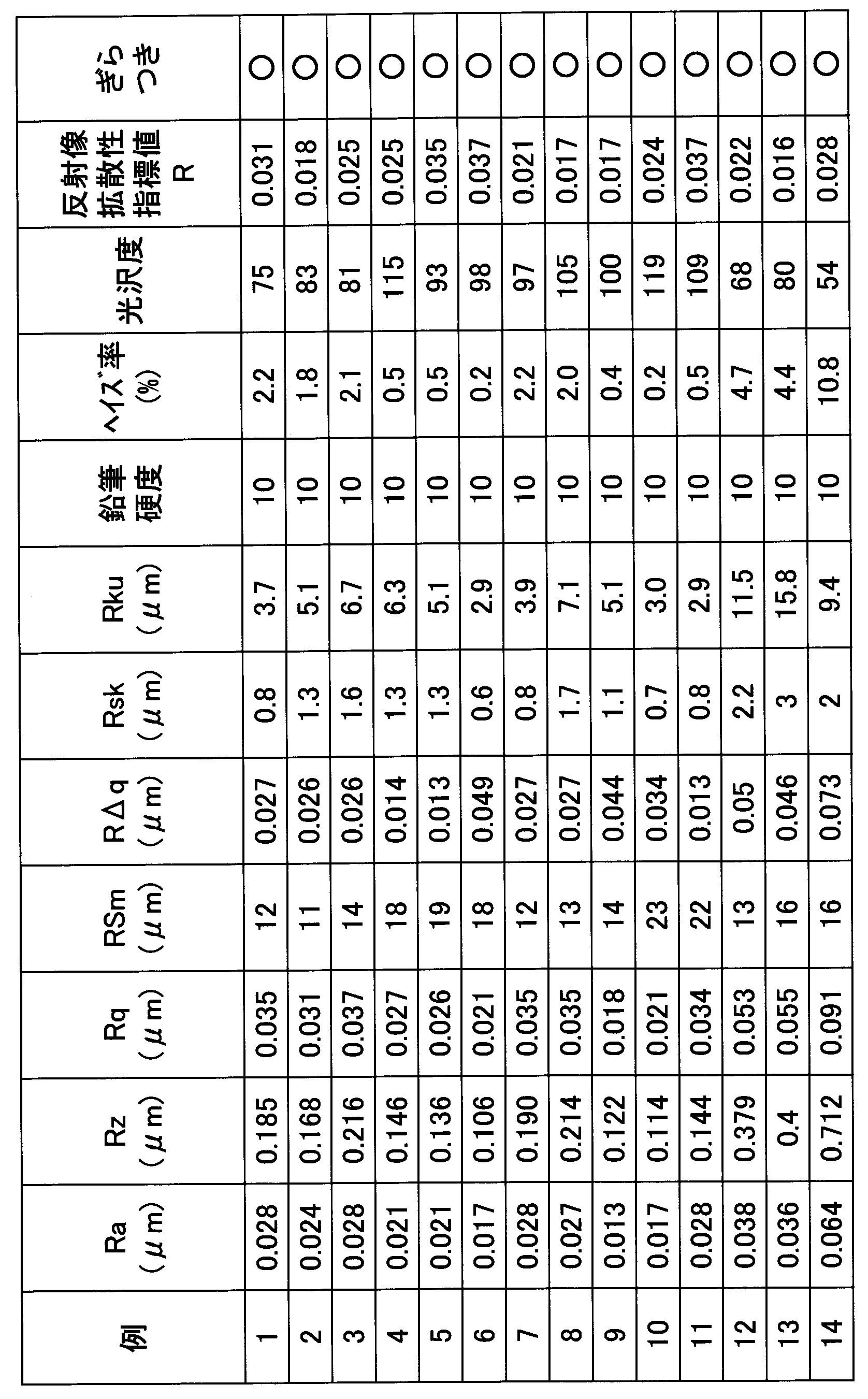
従って、例1~例14に係るカバー部材は、いずれも、外表面が平坦な表面となっており、かつ内表面は、凹凸表面であることがわかった。
また、耐擦傷性の評価結果から、例1~例14に係るカバー部材は、外表面が、いずれも10H以上の鉛筆硬度を有することがわかった。従って、これらのカバー部材を、凹凸層の側が表示素子の側となるように配置して使用した場合、良好な耐擦傷性が得られると言える。
また、例1~例14に係るカバー部材では、反射像拡散性指標値Rが、いずれも0.016以上となっている。このことから、例1~例14に係るカバー部材では、表示素子の上に配置した際に、外光の映り込みを有意に抑制できることがわかった。
また、例1~例14に係るカバー部材では、光沢度が130未満となっており、反射像による眩しさも、有意に抑制されることがわかった。また、例1~例14に係るカバー部材では、ぎらつきも、有意に抑制されていることがわかった。
さらに、例1~例13に係るカバー部材では、ヘイズが10%未満となっており、表示素子の上に配置した際に、画像の視認性を低下させるおそれは少ないことがわかった。
(例31)
以下の方法により、前述の図4に示したような構成のカバー部材を作製した。
以下の方法により、前述の図4に示したような構成のカバー部材を作製した。
なお、この例31において、透明基材および低反射層の構成は、前述の例7の場合と同様である。そこで、ここでは、凹凸層および反射層の形成方法について説明する。
(凹凸層の形成)
透明基材の第2の表面に、以下の方法で、凹凸層を形成した。
透明基材の第2の表面に、以下の方法で、凹凸層を形成した。
(塗布組成物の調製)
まず、前述の例1と同様の方法により、溶液Iを調製した。
まず、前述の例1と同様の方法により、溶液Iを調製した。
次に、166.1gの溶液Iに、233.9gのAP-11を加え、十分に撹拌した。これにより、凹凸層形成用の塗布組成物を得た。
(塗布組成物の塗布)
次に、前述の静電塗装ガンを備える静電塗装装置(液体静電コ一夕ー;旭サナック社製)を用いて、透明基材の第2の表面に、塗布組成物をスプレー塗布した。塗布の回数は、2回とした。
次に、前述の静電塗装ガンを備える静電塗装装置(液体静電コ一夕ー;旭サナック社製)を用いて、透明基材の第2の表面に、塗布組成物をスプレー塗布した。塗布の回数は、2回とした。
その後、塗布組成物を300℃で1時間焼成することにより、透明基材の第2の表面に凹凸層が形成された。
(反射層の形成)
次に、凹凸層の上に、反射層を形成した。
次に、凹凸層の上に、反射層を形成した。
反射層は、酸化ニオブ膜(波長632nmにおける屈折率は、約2.35)と酸化ケイ素膜(波長632nmにおける屈折率は、屈折率約1.47)の繰り返し構造とし、後反応スパッタ法により成膜した。繰り返し数は2.5回とし、すなわち、酸化ニオブ膜を3層、および酸化ケイ素膜を2層成膜した。
成膜条件は、例1における(低反射層の形成)の欄に示した条件と同様である。
各膜の厚さは、透明基材から近い順に、16.0nm(第1の酸化ニオブ膜)、34.75nm(第1の酸化ケイ素膜)、72.0nm(第2の酸化ニオブ膜)、17.5nm(第2の酸化ケイ素膜)、および20.0nm(第3の酸化ニオブ膜)とした。以下、係る構成の反射層を、「Re1」と称する。
以上の方法により、カバー部材(以下、「例31に係るカバー部材」と称する)が製造された。なお、例31に係るカバー部材において、低反射層の表面は、カバー部材の外表面に対応し、反射層の表面は、カバー部材の内表面に対応する。
(例32~例36)
例31と同様の方法により、カバー部材を作製した。
例31と同様の方法により、カバー部材を作製した。
ただし、これらの例32~例36では、凹凸層を形成する際に使用する塗布組成物に含まれる成分量、および静電塗装ガンによる塗布の回数を、例31の場合とは変化させた。
これにより、カバー部材(以下、それぞれ、「例32~例36に係るカバー部材」と称する)が製造された。
(例37)
例31と同様の方法により、カバー部材を作製した。
例31と同様の方法により、カバー部材を作製した。
ただし、この例37では、凹凸層の形成の際に、塗布組成物の塗布回数を3回とした。また、反射層の構成(膜厚)を、例31の場合とは変化させた。
すなわち、反射層は、透明基材から近い順に、16.0nm(第1の酸化ニオブ膜)、35.0nm(第1の酸化ケイ素膜)、64.0nm(第2の酸化ニオブ膜)、12.0nm(第2の酸化ケイ素膜)、および18.0nm(第3の酸化ニオブ膜)とした。以下、係る構成の反射層を、「Re2」と称する。
その他の製造条件は、例31の場合と同様である。これにより、カバー部材(以下、「例37に係るカバー部材」と称する)が製造された。
(例38~例41)
例37と同様の方法により、カバー部材を作製した。
例37と同様の方法により、カバー部材を作製した。
ただし、これらの例38~例41では、凹凸層を形成する際に使用する塗布組成物に含まれる成分量、および静電塗装ガンによる塗布の回数を、例37の場合とは変化させた。
これにより、カバー部材(以下、それぞれ、「例38~例41に係るカバー部材」と称する)が製造された。
以下の表3には、例31~例41に係るカバー部材における低反射層、凹凸層、および反射層の仕様などを、まとめて示した。
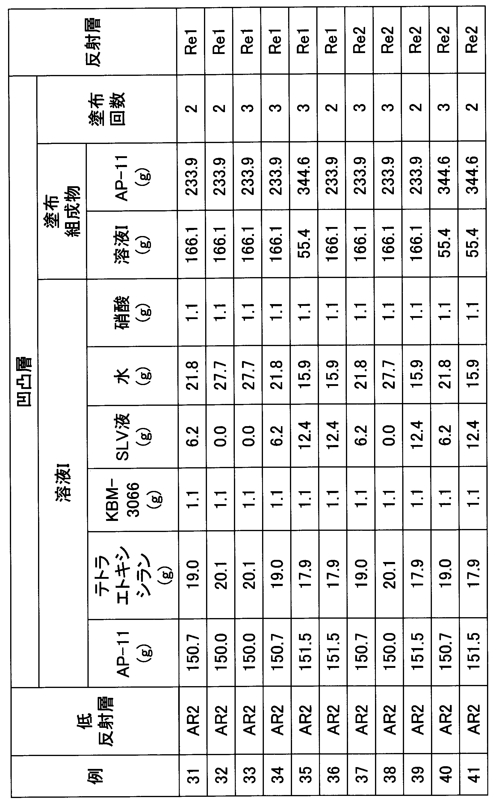
例31~例41に係るカバー部材を用いて、前述の評価を実施した。
以下の表4には、例31~例41に係るカバー部材において得られた評価結果を、まとめて示した。

従って、例31~例41に係るカバー部材は、いずれも、外表面が平坦な表面となっており、かつ内表面は、凹凸表面であることがわかった。
また、耐擦傷性の評価結果から、例31~例41に係るカバー部材は、外表面が、いずれも10H以上の鉛筆硬度を有することがわかった。従って、これらのカバー部材を、凹凸層の側が表示素子の側となるように配置して使用した場合、良好な耐擦傷性が得られると言える。
また、例31~例41に係るカバー部材では、反射像拡散性指標値Rが、いずれも0.03以上となっている。このことから、例31~例41に係るカバー部材では、表示素子の上に配置した際に、外光の映り込みを有意に抑制できることがわかった。
さらに、例31~例41に係るカバー部材では、ヘイズが20%未満となっており、表示素子の上に配置した際に、画像の視認性を低下させるおそれは少ないことがわかった。また、例31~例41に係るカバー部材では、ぎらつきも、有意に抑制されていることがわかった。また、例31~例39に係るカバー部材では、光沢度が85未満となっており、反射像による眩しさも、有意に抑制されることがわかった。
(例51)
以下の方法により、カバー部材を作製した。
以下の方法により、カバー部材を作製した。
まず、洗浄された透明基材を準備した。透明基材には、例1の場合と同様のガラス基板(FL1.1;旭硝子社製)を使用した。
次に、この透明基材の第1の表面に、凹凸層を形成した。凹凸層は、以下のように形成した。
まず、前述の例1と同様の方法により、溶液Iを調製した。
次に、110.7gの溶液Iに、289.3gのAP-11を加え、十分に撹拌した。これにより、凹凸層形成用の塗布組成物を得た。
次に、前述の静電塗装ガンを備える静電塗装装置を用いて、透明基材の第1の表面に、塗布組成物をスプレー塗布した。塗布の回数は、3回とした。
その後、塗布組成物を300℃で1時間焼成することにより、透明基材の第1の表面に凹凸層が形成された。
以上の方法により、カバー部材(以下、「例51に係るカバー部材」と称する)が製造された。なお、例51に係るカバー部材において、凹凸層の表面は、カバー部材の外表面に対応し、透明基材の第2の表面(第1の表面とは反対側の表面)は、カバー部材の内表面に対応する。
(例52)
例51と同様の方法により、カバー部材を作製した。
例51と同様の方法により、カバー部材を作製した。
ただし、この例52では、凹凸層を形成する際に使用する塗布組成物に含まれる成分量を、例51の場合とは変化させた。
これにより、カバー部材(以下「例52に係るカバー部材」と称する)が製造された。
以下の表5には、例51~例52に係るカバー部材における凹凸層の仕様を、まとめて示した。

例51~例52に係るカバー部材を用いて、前述の評価を実施した。
以下の表6には、例51~例52に係るカバー部材において得られた評価結果を、まとめて示した。
なお、例51~例52に係るカバー部材では、凹凸層の側が、線状光源装置507および面輝度測定器515の側となるようにして、反射像拡散性指標値Rの測定を実施した。

また、耐擦傷性の評価結果から、例51~例52に係るカバー部材は、外表面の鉛筆硬度が、いずれも6H程度しかないことがわかった。従って、これらのカバー部材を、透明基材の第2の表面の側が表示素子と面するように配置した場合、外表面は、あまり良好な耐擦傷性を有さないと言える。
このように、本発明の一実施形態による表示装置では、外部光の映り込みを有意に抑制することができる上、従来に比べてカバー部材の外表面の耐擦傷性を有意に高められることが確認された。
本願は、2018年1月15日に出願した日本国特許出願2018-004094号に基づく優先権を主張するものであり、同日本国出願の全内容を本願に参照により援用する。
100 第1の画像表示装置
110 カバー部材
112 カバー部材の外表面(平坦な表面)
114 カバー部材の内表面(凹凸表面)
120 透明基材
122 第1の表面
124 第2の表面
130 低反射層
170 表示素子
200 第2の画像表示装置
210 カバー部材
212 カバー部材の外表面(平坦表面)
214 カバー部材の内表面(凹凸表面)
220 透明基材
222 第1の表面
224 第2の表面
230 低反射層
240 凹凸層
270 表示素子
300 第3の画像表示装置
310 カバー部材
312 カバー部材の外表面(平坦な表面)
314 カバー部材の内表面(凹凸表面)
320 透明基材
322 第1の表面
324 第2の表面
330 低反射層
360 反射散乱層
370 表示素子
380 接着層
400 第4の画像表示装置
410 カバー部材
412 カバー部材の外表面(平坦な表面)
414 カバー部材の内表面(凹凸表面)
420 透明基材
422 第1の表面
424 第2の表面
430 低反射層
440 凹凸層
460 反射散乱層
470 表示素子
480 接着層
501 測定装置
507 線状光源装置
511 光源
512 黒色平板
515 面輝度測定器
520 カバー部材
522 外表面
531 第1の入射光
532 第1の反射光
533 第2の入射光
534 第2の反射光
S 空気層(隙間)
110 カバー部材
112 カバー部材の外表面(平坦な表面)
114 カバー部材の内表面(凹凸表面)
120 透明基材
122 第1の表面
124 第2の表面
130 低反射層
170 表示素子
200 第2の画像表示装置
210 カバー部材
212 カバー部材の外表面(平坦表面)
214 カバー部材の内表面(凹凸表面)
220 透明基材
222 第1の表面
224 第2の表面
230 低反射層
240 凹凸層
270 表示素子
300 第3の画像表示装置
310 カバー部材
312 カバー部材の外表面(平坦な表面)
314 カバー部材の内表面(凹凸表面)
320 透明基材
322 第1の表面
324 第2の表面
330 低反射層
360 反射散乱層
370 表示素子
380 接着層
400 第4の画像表示装置
410 カバー部材
412 カバー部材の外表面(平坦な表面)
414 カバー部材の内表面(凹凸表面)
420 透明基材
422 第1の表面
424 第2の表面
430 低反射層
440 凹凸層
460 反射散乱層
470 表示素子
480 接着層
501 測定装置
507 線状光源装置
511 光源
512 黒色平板
515 面輝度測定器
520 カバー部材
522 外表面
531 第1の入射光
532 第1の反射光
533 第2の入射光
534 第2の反射光
S 空気層(隙間)
Claims (14)
- 画像表示装置であって、
表示素子と、
該表示素子上に設置された、透明基材を有するカバー部材と、
を有し、
前記カバー部材は、前記表示素子の側に、凹凸表面を有し、前記表示素子とは反対の側に、平滑な外表面を有する、画像表示装置。 - 前記透明基材は、相互に対向する第1および第2の表面を有し、
前記透明基材の前記第1の表面には、前記平滑な外表面を形成する低反射層が設置される、請求項1に記載の画像表示装置。 - 前記透明基材の前記第2の表面は、前記凹凸表面である、請求項2に記載の画像表示装置。
- 前記透明基材の前記第2の表面には、前記凹凸表面を形成する凹凸層が設置される、請求項2に記載の画像表示装置。
- 前記カバー部材と前記表示素子との間には、空気層が設置される、請求項2乃至4のいずれか一つに記載の画像表示装置。
- 前記カバー部材は、ヘイズ率が10%以下である、請求項5に記載の画像表示装置。
- 前記カバー部材は、反射像拡散性指標値Rが0.015以上である、請求項5または6に記載の画像表示装置。
- 前記カバー部材は、光沢度が130未満である、請求項5乃至7のいずれか一つに記載の画像表示装置。
- 前記カバー部材は、前記表示素子の側に、前記凹凸表面を形成する反射散乱層を有し、
前記カバー部材と前記表示素子との間には、接着層が設置され、
前記接着層は、前記透明基材との屈折率の差nの絶対値Δnが0.07以下である、請求項2に記載の画像表示装置。 - 前記透明基材の前記第2の表面には、凹凸層が設置される、請求項9に記載の画像表示装置。
- 前記カバー部材は、ヘイズ率が20%未満である、請求項9または10に記載の画像表示装置。
- 前記カバー部材は、反射像拡散性指標値Rが0.03以上である、請求項9乃至11のいずれか一つに記載の画像表示装置。
- 前記カバー部材は、光沢度が85未満である、請求項9乃至12のいずれか一つに記載の画像表示装置。
- 前記表示素子は、液晶表示素子、有機EL表示素子、およびプラズマ表示素子のいずれか一つである、請求項1乃至13のいずれか一つに記載の画像表示装置。
Applications Claiming Priority (2)
| Application Number | Priority Date | Filing Date | Title |
|---|---|---|---|
| JP2018-004094 | 2018-01-15 | ||
| JP2018004094A JP2021056250A (ja) | 2018-01-15 | 2018-01-15 | 画像表示装置 |
Publications (1)
| Publication Number | Publication Date |
|---|---|
| WO2019138751A1 true WO2019138751A1 (ja) | 2019-07-18 |
Family
ID=67218273
Family Applications (1)
| Application Number | Title | Priority Date | Filing Date |
|---|---|---|---|
| PCT/JP2018/045136 Ceased WO2019138751A1 (ja) | 2018-01-15 | 2018-12-07 | 画像表示装置 |
Country Status (2)
| Country | Link |
|---|---|
| JP (1) | JP2021056250A (ja) |
| WO (1) | WO2019138751A1 (ja) |
Cited By (3)
| Publication number | Priority date | Publication date | Assignee | Title |
|---|---|---|---|---|
| JP2023510080A (ja) * | 2019-11-25 | 2023-03-13 | アイピーシー ワークス リミテッド | 光フィルタ及びその方法 |
| WO2023163149A1 (ja) * | 2022-02-28 | 2023-08-31 | 日東電工株式会社 | Oled表示装置用光学積層体 |
| WO2025023002A1 (ja) * | 2023-07-27 | 2025-01-30 | Agc株式会社 | 防眩カバーの製造方法、oledディスプレイユニットの製造方法、防眩カバー、及びoledディスプレイユニット |
Families Citing this family (2)
| Publication number | Priority date | Publication date | Assignee | Title |
|---|---|---|---|---|
| JP2023125926A (ja) * | 2022-02-28 | 2023-09-07 | Agc株式会社 | 自発光型表示装置 |
| JP2024121464A (ja) * | 2023-02-27 | 2024-09-06 | 三菱瓦斯化学株式会社 | 防眩性積層体及びその製造方法 |
Citations (5)
| Publication number | Priority date | Publication date | Assignee | Title |
|---|---|---|---|---|
| JP2006126628A (ja) * | 2004-10-29 | 2006-05-18 | Dainippon Printing Co Ltd | リバーシブル型光学用部材 |
| JP2009104103A (ja) * | 2007-10-01 | 2009-05-14 | Omron Corp | 反射防止シート、表示素子及びディスプレイ装置 |
| WO2013125312A1 (ja) * | 2012-02-20 | 2013-08-29 | シャープ株式会社 | 表示装置 |
| JP2014041206A (ja) * | 2012-08-21 | 2014-03-06 | Dainippon Printing Co Ltd | 光学フィルム用基材、光学フィルム、偏光板、液晶パネルおよび画像表示装置 |
| JP2017173736A (ja) * | 2016-03-25 | 2017-09-28 | 三菱ケミカル株式会社 | 粘着剤付き微細凹凸構造体および接合体 |
-
2018
- 2018-01-15 JP JP2018004094A patent/JP2021056250A/ja active Pending
- 2018-12-07 WO PCT/JP2018/045136 patent/WO2019138751A1/ja not_active Ceased
Patent Citations (5)
| Publication number | Priority date | Publication date | Assignee | Title |
|---|---|---|---|---|
| JP2006126628A (ja) * | 2004-10-29 | 2006-05-18 | Dainippon Printing Co Ltd | リバーシブル型光学用部材 |
| JP2009104103A (ja) * | 2007-10-01 | 2009-05-14 | Omron Corp | 反射防止シート、表示素子及びディスプレイ装置 |
| WO2013125312A1 (ja) * | 2012-02-20 | 2013-08-29 | シャープ株式会社 | 表示装置 |
| JP2014041206A (ja) * | 2012-08-21 | 2014-03-06 | Dainippon Printing Co Ltd | 光学フィルム用基材、光学フィルム、偏光板、液晶パネルおよび画像表示装置 |
| JP2017173736A (ja) * | 2016-03-25 | 2017-09-28 | 三菱ケミカル株式会社 | 粘着剤付き微細凹凸構造体および接合体 |
Cited By (4)
| Publication number | Priority date | Publication date | Assignee | Title |
|---|---|---|---|---|
| JP2023510080A (ja) * | 2019-11-25 | 2023-03-13 | アイピーシー ワークス リミテッド | 光フィルタ及びその方法 |
| US12481092B2 (en) | 2019-11-25 | 2025-11-25 | Innoworks Product Creation Limited | Light filter and the method thereof |
| WO2023163149A1 (ja) * | 2022-02-28 | 2023-08-31 | 日東電工株式会社 | Oled表示装置用光学積層体 |
| WO2025023002A1 (ja) * | 2023-07-27 | 2025-01-30 | Agc株式会社 | 防眩カバーの製造方法、oledディスプレイユニットの製造方法、防眩カバー、及びoledディスプレイユニット |
Also Published As
| Publication number | Publication date |
|---|---|
| JP2021056250A (ja) | 2021-04-08 |
Similar Documents
| Publication | Publication Date | Title |
|---|---|---|
| US11772356B2 (en) | Translucent structure | |
| CN107918167B (zh) | 带防眩膜的基体、用于形成防眩膜的液态组合物和带防眩膜的基体的制造方法 | |
| JP7010324B2 (ja) | 防眩膜付基体 | |
| US10802318B2 (en) | Transparent substrate with antifouling film and capacitance in-cell touch panel-type liquid crystal display device | |
| JP2019144475A (ja) | 透光性構造体 | |
| JP2021056250A (ja) | 画像表示装置 | |
| WO2012086806A1 (ja) | 低反射膜を有する物品 | |
| TW201433830A (zh) | 介電鏡體 | |
| JP7298071B2 (ja) | 防眩膜付き透明基体 | |
| US20200055771A1 (en) | Film-attached glass substrate, article, and method for producing film-attached glass substrate | |
| JP7151710B2 (ja) | 表示装置用の前面板 | |
| US20170291392A1 (en) | Article having low reflection film | |
| JP6164120B2 (ja) | 反射防止膜付き基材および物品 | |
| WO2019073946A1 (ja) | カバー部材 | |
| JP7563019B2 (ja) | カバーガラス | |
| JP7847984B2 (ja) | カバーガラス及びデジタルサイネージ | |
| JP2021092693A (ja) | カバーガラス | |
| TW202200360A (zh) | 遮光構件 | |
| WO2024248071A1 (ja) | 反射防止膜付透明基体および画像表示装置 | |
| JP2024006900A (ja) | 膜付きガラス基板及びその製造方法 | |
| WO2024004707A1 (ja) | 膜付きガラス基板及びその製造方法 |
Legal Events
| Date | Code | Title | Description |
|---|---|---|---|
| 121 | Ep: the epo has been informed by wipo that ep was designated in this application |
Ref document number: 18899614 Country of ref document: EP Kind code of ref document: A1 |
|
| NENP | Non-entry into the national phase |
Ref country code: DE |
|
| 122 | Ep: pct application non-entry in european phase |
Ref document number: 18899614 Country of ref document: EP Kind code of ref document: A1 |
|
| NENP | Non-entry into the national phase |
Ref country code: JP |