WO2019124415A1 - Charge-transporting varnish - Google Patents
Charge-transporting varnish Download PDFInfo
- Publication number
- WO2019124415A1 WO2019124415A1 PCT/JP2018/046693 JP2018046693W WO2019124415A1 WO 2019124415 A1 WO2019124415 A1 WO 2019124415A1 JP 2018046693 W JP2018046693 W JP 2018046693W WO 2019124415 A1 WO2019124415 A1 WO 2019124415A1
- Authority
- WO
- WIPO (PCT)
- Prior art keywords
- group
- carbon atoms
- charge transporting
- compound
- bis
- Prior art date
Links
- 239000002966 varnish Substances 0.000 title claims abstract description 135
- -1 aryl sulfonate ester compound Chemical class 0.000 claims abstract description 302
- 229910052757 nitrogen Inorganic materials 0.000 claims abstract description 29
- 125000004433 nitrogen atom Chemical group N* 0.000 claims abstract description 24
- 239000003960 organic solvent Substances 0.000 claims abstract description 16
- 125000005264 aryl amine group Chemical group 0.000 claims abstract description 9
- 125000004432 carbon atom Chemical group C* 0.000 claims description 176
- 125000003118 aryl group Chemical group 0.000 claims description 87
- 125000000217 alkyl group Chemical group 0.000 claims description 71
- 125000004435 hydrogen atom Chemical group [H]* 0.000 claims description 66
- 150000001875 compounds Chemical class 0.000 claims description 60
- 150000002430 hydrocarbons Chemical group 0.000 claims description 48
- 125000005843 halogen group Chemical group 0.000 claims description 45
- 239000010409 thin film Substances 0.000 claims description 38
- 239000002253 acid Substances 0.000 claims description 30
- UFWIBTONFRDIAS-UHFFFAOYSA-N Naphthalene Chemical compound C1=CC=CC2=CC=CC=C21 UFWIBTONFRDIAS-UHFFFAOYSA-N 0.000 claims description 28
- 125000001424 substituent group Chemical group 0.000 claims description 28
- 125000004093 cyano group Chemical group *C#N 0.000 claims description 26
- MWPLVEDNUUSJAV-UHFFFAOYSA-N anthracene Chemical compound C1=CC=CC2=CC3=CC=CC=C3C=C21 MWPLVEDNUUSJAV-UHFFFAOYSA-N 0.000 claims description 24
- 125000001931 aliphatic group Chemical group 0.000 claims description 21
- 229910052799 carbon Inorganic materials 0.000 claims description 21
- 125000001153 fluoro group Chemical group F* 0.000 claims description 21
- 229910052731 fluorine Inorganic materials 0.000 claims description 20
- 125000000449 nitro group Chemical group [O-][N+](*)=O 0.000 claims description 19
- 125000003342 alkenyl group Chemical group 0.000 claims description 18
- OKTJSMMVPCPJKN-UHFFFAOYSA-N Carbon Chemical compound [C] OKTJSMMVPCPJKN-UHFFFAOYSA-N 0.000 claims description 13
- 125000002947 alkylene group Chemical group 0.000 claims description 9
- ONUFSRWQCKNVSL-UHFFFAOYSA-N 1,2,3,4,5-pentafluoro-6-(2,3,4,5,6-pentafluorophenyl)benzene Chemical group FC1=C(F)C(F)=C(F)C(F)=C1C1=C(F)C(F)=C(F)C(F)=C1F ONUFSRWQCKNVSL-UHFFFAOYSA-N 0.000 claims description 5
- 125000002915 carbonyl group Chemical group [*:2]C([*:1])=O 0.000 claims description 4
- 239000011737 fluorine Substances 0.000 claims description 3
- YCKRFDGAMUMZLT-UHFFFAOYSA-N Fluorine atom Chemical group [F] YCKRFDGAMUMZLT-UHFFFAOYSA-N 0.000 claims description 2
- 125000005313 fatty acid group Chemical group 0.000 claims description 2
- 239000010410 layer Substances 0.000 description 137
- 238000000034 method Methods 0.000 description 60
- 239000000758 substrate Substances 0.000 description 55
- 229910052741 iridium Inorganic materials 0.000 description 45
- 239000002904 solvent Substances 0.000 description 43
- GKOZUEZYRPOHIO-UHFFFAOYSA-N iridium atom Chemical compound [Ir] GKOZUEZYRPOHIO-UHFFFAOYSA-N 0.000 description 42
- 125000001997 phenyl group Chemical group [H]C1=C([H])C([H])=C(*)C([H])=C1[H] 0.000 description 40
- 238000002347 injection Methods 0.000 description 38
- 239000007924 injection Substances 0.000 description 38
- 238000007789 sealing Methods 0.000 description 37
- HEDRZPFGACZZDS-UHFFFAOYSA-N Chloroform Chemical compound ClC(Cl)Cl HEDRZPFGACZZDS-UHFFFAOYSA-N 0.000 description 34
- 230000000052 comparative effect Effects 0.000 description 28
- UHOVQNZJYSORNB-UHFFFAOYSA-N Benzene Chemical compound C1=CC=CC=C1 UHOVQNZJYSORNB-UHFFFAOYSA-N 0.000 description 27
- 239000000463 material Substances 0.000 description 26
- 239000000243 solution Substances 0.000 description 23
- YXFVVABEGXRONW-UHFFFAOYSA-N Toluene Chemical compound CC1=CC=CC=C1 YXFVVABEGXRONW-UHFFFAOYSA-N 0.000 description 21
- 239000010408 film Substances 0.000 description 19
- 125000002496 methyl group Chemical group [H]C([H])([H])* 0.000 description 19
- 239000011148 porous material Substances 0.000 description 19
- XEKOWRVHYACXOJ-UHFFFAOYSA-N Ethyl acetate Chemical compound CCOC(C)=O XEKOWRVHYACXOJ-UHFFFAOYSA-N 0.000 description 18
- ZUOUZKKEUPVFJK-UHFFFAOYSA-N diphenyl Chemical compound C1=CC=CC=C1C1=CC=CC=C1 ZUOUZKKEUPVFJK-UHFFFAOYSA-N 0.000 description 18
- 125000001495 ethyl group Chemical group [H]C([H])([H])C([H])([H])* 0.000 description 16
- 229910052782 aluminium Inorganic materials 0.000 description 15
- XAGFODPZIPBFFR-UHFFFAOYSA-N aluminium Chemical compound [Al] XAGFODPZIPBFFR-UHFFFAOYSA-N 0.000 description 15
- 125000001072 heteroaryl group Chemical group 0.000 description 15
- 230000005525 hole transport Effects 0.000 description 15
- JUJWROOIHBZHMG-UHFFFAOYSA-N Pyridine Chemical compound C1=CC=NC=C1 JUJWROOIHBZHMG-UHFFFAOYSA-N 0.000 description 14
- 239000003795 chemical substances by application Substances 0.000 description 14
- 125000004123 n-propyl group Chemical group [H]C([H])([H])C([H])([H])C([H])([H])* 0.000 description 14
- 239000007787 solid Substances 0.000 description 14
- FYSNRJHAOHDILO-UHFFFAOYSA-N thionyl chloride Chemical compound ClS(Cl)=O FYSNRJHAOHDILO-UHFFFAOYSA-N 0.000 description 14
- ZMXDDKWLCZADIW-UHFFFAOYSA-N N,N-Dimethylformamide Chemical compound CN(C)C=O ZMXDDKWLCZADIW-UHFFFAOYSA-N 0.000 description 13
- 239000000203 mixture Substances 0.000 description 13
- POILWHVDKZOXJZ-ARJAWSKDSA-M (z)-4-oxopent-2-en-2-olate Chemical compound C\C([O-])=C\C(C)=O POILWHVDKZOXJZ-ARJAWSKDSA-M 0.000 description 12
- 125000001637 1-naphthyl group Chemical group [H]C1=C([H])C([H])=C2C(*)=C([H])C([H])=C([H])C2=C1[H] 0.000 description 12
- 238000000151 deposition Methods 0.000 description 12
- 230000008021 deposition Effects 0.000 description 12
- 239000012046 mixed solvent Substances 0.000 description 12
- VLKZOEOYAKHREP-UHFFFAOYSA-N n-Hexane Chemical compound CCCCCC VLKZOEOYAKHREP-UHFFFAOYSA-N 0.000 description 12
- 239000000126 substance Substances 0.000 description 12
- 125000000999 tert-butyl group Chemical group [H]C([H])([H])C(*)(C([H])([H])[H])C([H])([H])[H] 0.000 description 12
- WZFUQSJFWNHZHM-UHFFFAOYSA-N 2-[4-[2-(2,3-dihydro-1H-inden-2-ylamino)pyrimidin-5-yl]piperazin-1-yl]-1-(2,4,6,7-tetrahydrotriazolo[4,5-c]pyridin-5-yl)ethanone Chemical compound C1C(CC2=CC=CC=C12)NC1=NC=C(C=N1)N1CCN(CC1)CC(=O)N1CC2=C(CC1)NN=N2 WZFUQSJFWNHZHM-UHFFFAOYSA-N 0.000 description 11
- 125000001622 2-naphthyl group Chemical group [H]C1=C([H])C([H])=C2C([H])=C(*)C([H])=C([H])C2=C1[H] 0.000 description 11
- 239000007983 Tris buffer Substances 0.000 description 11
- 230000015572 biosynthetic process Effects 0.000 description 11
- 125000000959 isobutyl group Chemical group [H]C([H])([H])C([H])(C([H])([H])[H])C([H])([H])* 0.000 description 11
- 125000001449 isopropyl group Chemical group [H]C([H])([H])C([H])(*)C([H])([H])[H] 0.000 description 11
- 125000004108 n-butyl group Chemical group [H]C([H])([H])C([H])([H])C([H])([H])C([H])([H])* 0.000 description 11
- 229920000642 polymer Polymers 0.000 description 11
- 239000004810 polytetrafluoroethylene Substances 0.000 description 11
- 229920001343 polytetrafluoroethylene Polymers 0.000 description 11
- 239000002356 single layer Substances 0.000 description 11
- 239000000853 adhesive Substances 0.000 description 10
- 230000001070 adhesive effect Effects 0.000 description 10
- QVGXLLKOCUKJST-UHFFFAOYSA-N atomic oxygen Chemical compound [O] QVGXLLKOCUKJST-UHFFFAOYSA-N 0.000 description 10
- 239000004305 biphenyl Substances 0.000 description 10
- 238000006243 chemical reaction Methods 0.000 description 10
- 238000004519 manufacturing process Methods 0.000 description 10
- 239000001301 oxygen Substances 0.000 description 10
- 229910052760 oxygen Inorganic materials 0.000 description 10
- 125000000391 vinyl group Chemical group [H]C([*])=C([H])[H] 0.000 description 10
- XLYOFNOQVPJJNP-UHFFFAOYSA-N water Substances O XLYOFNOQVPJJNP-UHFFFAOYSA-N 0.000 description 10
- YJLUBHOZZTYQIP-UHFFFAOYSA-N 2-[5-[2-(2,3-dihydro-1H-inden-2-ylamino)pyrimidin-5-yl]-1,3,4-oxadiazol-2-yl]-1-(2,4,6,7-tetrahydrotriazolo[4,5-c]pyridin-5-yl)ethanone Chemical compound C1C(CC2=CC=CC=C12)NC1=NC=C(C=N1)C1=NN=C(O1)CC(=O)N1CC2=C(CC1)NN=N2 YJLUBHOZZTYQIP-UHFFFAOYSA-N 0.000 description 9
- 235000010290 biphenyl Nutrition 0.000 description 9
- 238000000576 coating method Methods 0.000 description 9
- MTHSVFCYNBDYFN-UHFFFAOYSA-N diethylene glycol Chemical compound OCCOCCO MTHSVFCYNBDYFN-UHFFFAOYSA-N 0.000 description 9
- 125000001280 n-hexyl group Chemical group C(CCCCC)* 0.000 description 9
- 238000003786 synthesis reaction Methods 0.000 description 9
- CXWXQJXEFPUFDZ-UHFFFAOYSA-N tetralin Chemical compound C1=CC=C2CCCCC2=C1 CXWXQJXEFPUFDZ-UHFFFAOYSA-N 0.000 description 9
- CTQNGGLPUBDAKN-UHFFFAOYSA-N O-Xylene Chemical compound CC1=CC=CC=C1C CTQNGGLPUBDAKN-UHFFFAOYSA-N 0.000 description 8
- 150000001491 aromatic compounds Chemical class 0.000 description 8
- XSIFPSYPOVKYCO-UHFFFAOYSA-N butyl benzoate Chemical compound CCCCOC(=O)C1=CC=CC=C1 XSIFPSYPOVKYCO-UHFFFAOYSA-N 0.000 description 8
- 125000000113 cyclohexyl group Chemical group [H]C1([H])C([H])([H])C([H])([H])C([H])(*)C([H])([H])C1([H])[H] 0.000 description 8
- 125000001511 cyclopentyl group Chemical group [H]C1([H])C([H])([H])C([H])([H])C([H])(*)C1([H])[H] 0.000 description 8
- 239000002019 doping agent Substances 0.000 description 8
- 230000002140 halogenating effect Effects 0.000 description 8
- 125000003136 n-heptyl group Chemical group [H]C([H])([H])C([H])([H])C([H])([H])C([H])([H])C([H])([H])C([H])([H])C([H])([H])* 0.000 description 8
- 125000000740 n-pentyl group Chemical group [H]C([H])([H])C([H])([H])C([H])([H])C([H])([H])C([H])([H])* 0.000 description 8
- BBEAQIROQSPTKN-UHFFFAOYSA-N pyrene Chemical compound C1=CC=C2C=CC3=CC=CC4=CC=C1C2=C43 BBEAQIROQSPTKN-UHFFFAOYSA-N 0.000 description 8
- 125000002914 sec-butyl group Chemical group [H]C([H])([H])C([H])([H])C([H])(*)C([H])([H])[H] 0.000 description 8
- 239000008096 xylene Substances 0.000 description 8
- HMUNWXXNJPVALC-UHFFFAOYSA-N 1-[4-[2-(2,3-dihydro-1H-inden-2-ylamino)pyrimidin-5-yl]piperazin-1-yl]-2-(2,4,6,7-tetrahydrotriazolo[4,5-c]pyridin-5-yl)ethanone Chemical compound C1C(CC2=CC=CC=C12)NC1=NC=C(C=N1)N1CCN(CC1)C(CN1CC2=C(CC1)NN=N2)=O HMUNWXXNJPVALC-UHFFFAOYSA-N 0.000 description 7
- 238000005160 1H NMR spectroscopy Methods 0.000 description 7
- 125000004975 3-butenyl group Chemical group C(CC=C)* 0.000 description 7
- 125000001309 chloro group Chemical group Cl* 0.000 description 7
- 125000004122 cyclic group Chemical group 0.000 description 7
- 238000010438 heat treatment Methods 0.000 description 7
- PQXKHYXIUOZZFA-UHFFFAOYSA-M lithium fluoride Chemical compound [Li+].[F-] PQXKHYXIUOZZFA-UHFFFAOYSA-M 0.000 description 7
- IBHBKWKFFTZAHE-UHFFFAOYSA-N n-[4-[4-(n-naphthalen-1-ylanilino)phenyl]phenyl]-n-phenylnaphthalen-1-amine Chemical compound C1=CC=CC=C1N(C=1C2=CC=CC=C2C=CC=1)C1=CC=C(C=2C=CC(=CC=2)N(C=2C=CC=CC=2)C=2C3=CC=CC=C3C=CC=2)C=C1 IBHBKWKFFTZAHE-UHFFFAOYSA-N 0.000 description 7
- 239000012299 nitrogen atmosphere Substances 0.000 description 7
- 239000002798 polar solvent Substances 0.000 description 7
- 238000007740 vapor deposition Methods 0.000 description 7
- CHLICZRVGGXEOD-UHFFFAOYSA-N 1-Methoxy-4-methylbenzene Chemical compound COC1=CC=C(C)C=C1 CHLICZRVGGXEOD-UHFFFAOYSA-N 0.000 description 6
- 125000004973 1-butenyl group Chemical group C(=CCC)* 0.000 description 6
- 125000006021 1-methyl-2-propenyl group Chemical group 0.000 description 6
- 125000006017 1-propenyl group Chemical group 0.000 description 6
- FSEXLNMNADBYJU-UHFFFAOYSA-N 2-phenylquinoline Chemical compound C1=CC=CC=C1C1=CC=C(C=CC=C2)C2=N1 FSEXLNMNADBYJU-UHFFFAOYSA-N 0.000 description 6
- WYURNTSHIVDZCO-UHFFFAOYSA-N Tetrahydrofuran Chemical compound C1CCOC1 WYURNTSHIVDZCO-UHFFFAOYSA-N 0.000 description 6
- ZMANZCXQSJIPKH-UHFFFAOYSA-N Triethylamine Chemical compound CCN(CC)CC ZMANZCXQSJIPKH-UHFFFAOYSA-N 0.000 description 6
- 239000012298 atmosphere Substances 0.000 description 6
- 239000011248 coating agent Substances 0.000 description 6
- MHDVGSVTJDSBDK-UHFFFAOYSA-N dibenzyl ether Chemical compound C=1C=CC=CC=1COCC1=CC=CC=C1 MHDVGSVTJDSBDK-UHFFFAOYSA-N 0.000 description 6
- MTZQAGJQAFMTAQ-UHFFFAOYSA-N ethyl benzoate Chemical compound CCOC(=O)C1=CC=CC=C1 MTZQAGJQAFMTAQ-UHFFFAOYSA-N 0.000 description 6
- 125000000555 isopropenyl group Chemical group [H]\C([H])=C(\*)C([H])([H])[H] 0.000 description 6
- UMJSCPRVCHMLSP-UHFFFAOYSA-N pyridine Natural products COC1=CC=CN=C1 UMJSCPRVCHMLSP-UHFFFAOYSA-N 0.000 description 6
- 125000001140 1,4-phenylene group Chemical group [H]C1=C([H])C([*:2])=C([H])C([H])=C1[*:1] 0.000 description 5
- 125000004974 2-butenyl group Chemical group C(C=CC)* 0.000 description 5
- 125000003903 2-propenyl group Chemical group [H]C([*])([H])C([H])=C([H])[H] 0.000 description 5
- CONKBQPVFMXDOV-QHCPKHFHSA-N 6-[(5S)-5-[[4-[2-(2,3-dihydro-1H-inden-2-ylamino)pyrimidin-5-yl]piperazin-1-yl]methyl]-2-oxo-1,3-oxazolidin-3-yl]-3H-1,3-benzoxazol-2-one Chemical compound C1C(CC2=CC=CC=C12)NC1=NC=C(C=N1)N1CCN(CC1)C[C@H]1CN(C(O1)=O)C1=CC2=C(NC(O2)=O)C=C1 CONKBQPVFMXDOV-QHCPKHFHSA-N 0.000 description 5
- 125000000304 alkynyl group Chemical group 0.000 description 5
- 239000010405 anode material Substances 0.000 description 5
- 125000002078 anthracen-1-yl group Chemical group [H]C1=C([H])C([H])=C2C([H])=C3C([*])=C([H])C([H])=C([H])C3=C([H])C2=C1[H] 0.000 description 5
- 125000000748 anthracen-2-yl group Chemical group [H]C1=C([H])C([H])=C2C([H])=C3C([H])=C([*])C([H])=C([H])C3=C([H])C2=C1[H] 0.000 description 5
- 230000000903 blocking effect Effects 0.000 description 5
- 230000015556 catabolic process Effects 0.000 description 5
- 238000006731 degradation reaction Methods 0.000 description 5
- 238000001035 drying Methods 0.000 description 5
- 238000001914 filtration Methods 0.000 description 5
- 125000006038 hexenyl group Chemical group 0.000 description 5
- 238000005259 measurement Methods 0.000 description 5
- 229910052751 metal Inorganic materials 0.000 description 5
- 239000002184 metal Substances 0.000 description 5
- 230000007935 neutral effect Effects 0.000 description 5
- 239000011734 sodium Substances 0.000 description 5
- KBPLFHHGFOOTCA-UHFFFAOYSA-N 1-Octanol Chemical compound CCCCCCCCO KBPLFHHGFOOTCA-UHFFFAOYSA-N 0.000 description 4
- JOLQKTGDSGKSKJ-UHFFFAOYSA-N 1-ethoxypropan-2-ol Chemical compound CCOCC(C)O JOLQKTGDSGKSKJ-UHFFFAOYSA-N 0.000 description 4
- PRPINYUDVPFIRX-UHFFFAOYSA-N 1-naphthaleneacetic acid Chemical compound C1=CC=C2C(CC(=O)O)=CC=CC2=C1 PRPINYUDVPFIRX-UHFFFAOYSA-N 0.000 description 4
- IJGRMHOSHXDMSA-UHFFFAOYSA-N Atomic nitrogen Chemical compound N#N IJGRMHOSHXDMSA-UHFFFAOYSA-N 0.000 description 4
- WKBOTKDWSSQWDR-UHFFFAOYSA-N Bromine atom Chemical group [Br] WKBOTKDWSSQWDR-UHFFFAOYSA-N 0.000 description 4
- 239000004215 Carbon black (E152) Substances 0.000 description 4
- 125000002252 acyl group Chemical group 0.000 description 4
- XJHCXCQVJFPJIK-UHFFFAOYSA-M caesium fluoride Chemical compound [F-].[Cs+] XJHCXCQVJFPJIK-UHFFFAOYSA-M 0.000 description 4
- 239000003054 catalyst Substances 0.000 description 4
- 229910052801 chlorine Inorganic materials 0.000 description 4
- 238000004140 cleaning Methods 0.000 description 4
- 239000012043 crude product Substances 0.000 description 4
- 238000000605 extraction Methods 0.000 description 4
- GVEPBJHOBDJJJI-UHFFFAOYSA-N fluoranthrene Natural products C1=CC(C2=CC=CC=C22)=C3C2=CC=CC3=C1 GVEPBJHOBDJJJI-UHFFFAOYSA-N 0.000 description 4
- 229930195733 hydrocarbon Natural products 0.000 description 4
- AWJUIBRHMBBTKR-UHFFFAOYSA-N isoquinoline Chemical compound C1=NC=CC2=CC=CC=C21 AWJUIBRHMBBTKR-UHFFFAOYSA-N 0.000 description 4
- 125000001624 naphthyl group Chemical group 0.000 description 4
- 239000012044 organic layer Substances 0.000 description 4
- 125000001181 organosilyl group Chemical group [SiH3]* 0.000 description 4
- 125000001037 p-tolyl group Chemical group [H]C1=C([H])C(=C([H])C([H])=C1*)C([H])([H])[H] 0.000 description 4
- BASFCYQUMIYNBI-UHFFFAOYSA-N platinum Chemical compound [Pt] BASFCYQUMIYNBI-UHFFFAOYSA-N 0.000 description 4
- 239000002861 polymer material Substances 0.000 description 4
- 238000002360 preparation method Methods 0.000 description 4
- 238000000746 purification Methods 0.000 description 4
- 125000005504 styryl group Chemical group 0.000 description 4
- 125000002023 trifluoromethyl group Chemical group FC(F)(F)* 0.000 description 4
- 229920002554 vinyl polymer Polymers 0.000 description 4
- SNAQINZKMQFYFV-UHFFFAOYSA-N 1-[2-[2-(2-methoxyethoxy)ethoxy]ethoxy]butane Chemical compound CCCCOCCOCCOCCOC SNAQINZKMQFYFV-UHFFFAOYSA-N 0.000 description 3
- UDONPJKEOAWFGI-UHFFFAOYSA-N 1-methyl-3-phenoxybenzene Chemical compound CC1=CC=CC(OC=2C=CC=CC=2)=C1 UDONPJKEOAWFGI-UHFFFAOYSA-N 0.000 description 3
- VZSRBBMJRBPUNF-UHFFFAOYSA-N 2-(2,3-dihydro-1H-inden-2-ylamino)-N-[3-oxo-3-(2,4,6,7-tetrahydrotriazolo[4,5-c]pyridin-5-yl)propyl]pyrimidine-5-carboxamide Chemical compound C1C(CC2=CC=CC=C12)NC1=NC=C(C=N1)C(=O)NCCC(N1CC2=C(CC1)NN=N2)=O VZSRBBMJRBPUNF-UHFFFAOYSA-N 0.000 description 3
- POXIZPBFFUKMEQ-UHFFFAOYSA-N 2-cyanoethenylideneazanide Chemical group [N-]=C=[C+]C#N POXIZPBFFUKMEQ-UHFFFAOYSA-N 0.000 description 3
- 125000004105 2-pyridyl group Chemical group N1=C([*])C([H])=C([H])C([H])=C1[H] 0.000 description 3
- 125000003349 3-pyridyl group Chemical group N1=C([H])C([*])=C([H])C([H])=C1[H] 0.000 description 3
- ZCYVEMRRCGMTRW-UHFFFAOYSA-N 7553-56-2 Chemical group [I] ZCYVEMRRCGMTRW-UHFFFAOYSA-N 0.000 description 3
- WEVYAHXRMPXWCK-UHFFFAOYSA-N Acetonitrile Chemical compound CC#N WEVYAHXRMPXWCK-UHFFFAOYSA-N 0.000 description 3
- LYCAIKOWRPUZTN-UHFFFAOYSA-N Ethylene glycol Chemical compound OCCO LYCAIKOWRPUZTN-UHFFFAOYSA-N 0.000 description 3
- OKKJLVBELUTLKV-UHFFFAOYSA-N Methanol Chemical compound OC OKKJLVBELUTLKV-UHFFFAOYSA-N 0.000 description 3
- NBIIXXVUZAFLBC-UHFFFAOYSA-N Phosphoric acid Chemical group OP(O)(O)=O NBIIXXVUZAFLBC-UHFFFAOYSA-N 0.000 description 3
- PMZURENOXWZQFD-UHFFFAOYSA-L Sodium Sulfate Chemical compound [Na+].[Na+].[O-]S([O-])(=O)=O PMZURENOXWZQFD-UHFFFAOYSA-L 0.000 description 3
- 125000003277 amino group Chemical group 0.000 description 3
- 150000001721 carbon Chemical group 0.000 description 3
- 239000010406 cathode material Substances 0.000 description 3
- 238000012512 characterization method Methods 0.000 description 3
- 239000007810 chemical reaction solvent Substances 0.000 description 3
- HHNHBFLGXIUXCM-GFCCVEGCSA-N cyclohexylbenzene Chemical compound [CH]1CCCC[C@@H]1C1=CC=CC=C1 HHNHBFLGXIUXCM-GFCCVEGCSA-N 0.000 description 3
- WVIIMZNLDWSIRH-UHFFFAOYSA-N cyclohexylcyclohexane Chemical group C1CCCCC1C1CCCCC1 WVIIMZNLDWSIRH-UHFFFAOYSA-N 0.000 description 3
- 238000001704 evaporation Methods 0.000 description 3
- 230000008020 evaporation Effects 0.000 description 3
- RAXXELZNTBOGNW-UHFFFAOYSA-N imidazole Natural products C1=CNC=N1 RAXXELZNTBOGNW-UHFFFAOYSA-N 0.000 description 3
- 229910052740 iodine Inorganic materials 0.000 description 3
- MILUBEOXRNEUHS-UHFFFAOYSA-N iridium(3+) Chemical compound [Ir+3] MILUBEOXRNEUHS-UHFFFAOYSA-N 0.000 description 3
- 125000000611 organothio group Chemical group 0.000 description 3
- 125000005561 phenanthryl group Chemical group 0.000 description 3
- 229920000123 polythiophene Polymers 0.000 description 3
- BWHMMNNQKKPAPP-UHFFFAOYSA-L potassium carbonate Chemical compound [K+].[K+].[O-]C([O-])=O BWHMMNNQKKPAPP-UHFFFAOYSA-L 0.000 description 3
- 125000002924 primary amino group Chemical group [H]N([H])* 0.000 description 3
- 239000000047 product Substances 0.000 description 3
- 238000010992 reflux Methods 0.000 description 3
- 229910000077 silane Inorganic materials 0.000 description 3
- 238000010898 silica gel chromatography Methods 0.000 description 3
- 229910052938 sodium sulfate Inorganic materials 0.000 description 3
- 235000011152 sodium sulphate Nutrition 0.000 description 3
- 125000002130 sulfonic acid ester group Chemical group 0.000 description 3
- 238000004381 surface treatment Methods 0.000 description 3
- YLQBMQCUIZJEEH-UHFFFAOYSA-N tetrahydrofuran Natural products C=1C=COC=1 YLQBMQCUIZJEEH-UHFFFAOYSA-N 0.000 description 3
- 125000003944 tolyl group Chemical group 0.000 description 3
- YFNKIDBQEZZDLK-UHFFFAOYSA-N triglyme Chemical compound COCCOCCOCCOC YFNKIDBQEZZDLK-UHFFFAOYSA-N 0.000 description 3
- PUPZLCDOIYMWBV-UHFFFAOYSA-N (+/-)-1,3-Butanediol Chemical compound CC(O)CCO PUPZLCDOIYMWBV-UHFFFAOYSA-N 0.000 description 2
- SCYULBFZEHDVBN-UHFFFAOYSA-N 1,1-Dichloroethane Chemical compound CC(Cl)Cl SCYULBFZEHDVBN-UHFFFAOYSA-N 0.000 description 2
- 125000001989 1,3-phenylene group Chemical group [H]C1=C([H])C([*:1])=C([H])C([*:2])=C1[H] 0.000 description 2
- KZEVSDGEBAJOTK-UHFFFAOYSA-N 1-(2,4,6,7-tetrahydrotriazolo[4,5-c]pyridin-5-yl)-2-[5-[2-[[3-(trifluoromethoxy)phenyl]methylamino]pyrimidin-5-yl]-1,3,4-oxadiazol-2-yl]ethanone Chemical compound N1N=NC=2CN(CCC=21)C(CC=1OC(=NN=1)C=1C=NC(=NC=1)NCC1=CC(=CC=C1)OC(F)(F)F)=O KZEVSDGEBAJOTK-UHFFFAOYSA-N 0.000 description 2
- WFQFDAGQJUVDKP-UHFFFAOYSA-N 2,8-ditert-butyl-5,11-bis(4-tert-butylphenyl)-6,12-diphenyltetracene Chemical compound C1=CC(C(C)(C)C)=CC=C1C(C1=C(C=2C=CC=CC=2)C2=CC(=CC=C2C(C=2C=CC(=CC=2)C(C)(C)C)=C11)C(C)(C)C)=C(C=CC(=C2)C(C)(C)C)C2=C1C1=CC=CC=C1 WFQFDAGQJUVDKP-UHFFFAOYSA-N 0.000 description 2
- LDXJRKWFNNFDSA-UHFFFAOYSA-N 2-(2,4,6,7-tetrahydrotriazolo[4,5-c]pyridin-5-yl)-1-[4-[2-[[3-(trifluoromethoxy)phenyl]methylamino]pyrimidin-5-yl]piperazin-1-yl]ethanone Chemical compound C1CN(CC2=NNN=C21)CC(=O)N3CCN(CC3)C4=CN=C(N=C4)NCC5=CC(=CC=C5)OC(F)(F)F LDXJRKWFNNFDSA-UHFFFAOYSA-N 0.000 description 2
- ZWEHNKRNPOVVGH-UHFFFAOYSA-N 2-Butanone Chemical compound CCC(C)=O ZWEHNKRNPOVVGH-UHFFFAOYSA-N 0.000 description 2
- XMVBHZBLHNOQON-UHFFFAOYSA-N 2-butyl-1-octanol Chemical compound CCCCCCC(CO)CCCC XMVBHZBLHNOQON-UHFFFAOYSA-N 0.000 description 2
- VQGHOUODWALEFC-UHFFFAOYSA-N 2-phenylpyridine Chemical compound C1=CC=CC=C1C1=CC=CC=N1 VQGHOUODWALEFC-UHFFFAOYSA-N 0.000 description 2
- GYSCXPVAKHVAAY-UHFFFAOYSA-N 3-Nonanol Chemical compound CCCCCCC(O)CC GYSCXPVAKHVAAY-UHFFFAOYSA-N 0.000 description 2
- 125000000339 4-pyridyl group Chemical group N1=C([H])C([H])=C([*])C([H])=C1[H] 0.000 description 2
- XKRFYHLGVUSROY-UHFFFAOYSA-N Argon Chemical compound [Ar] XKRFYHLGVUSROY-UHFFFAOYSA-N 0.000 description 2
- LSNNMFCWUKXFEE-UHFFFAOYSA-M Bisulfite Chemical compound OS([O-])=O LSNNMFCWUKXFEE-UHFFFAOYSA-M 0.000 description 2
- IAZDPXIOMUYVGZ-UHFFFAOYSA-N Dimethylsulphoxide Chemical compound CS(C)=O IAZDPXIOMUYVGZ-UHFFFAOYSA-N 0.000 description 2
- LFQSCWFLJHTTHZ-UHFFFAOYSA-N Ethanol Chemical compound CCO LFQSCWFLJHTTHZ-UHFFFAOYSA-N 0.000 description 2
- YNQLUTRBYVCPMQ-UHFFFAOYSA-N Ethylbenzene Chemical compound CCC1=CC=CC=C1 YNQLUTRBYVCPMQ-UHFFFAOYSA-N 0.000 description 2
- DGAQECJNVWCQMB-PUAWFVPOSA-M Ilexoside XXIX Chemical compound C[C@@H]1CC[C@@]2(CC[C@@]3(C(=CC[C@H]4[C@]3(CC[C@@H]5[C@@]4(CC[C@@H](C5(C)C)OS(=O)(=O)[O-])C)C)[C@@H]2[C@]1(C)O)C)C(=O)O[C@H]6[C@@H]([C@H]([C@@H]([C@H](O6)CO)O)O)O.[Na+] DGAQECJNVWCQMB-PUAWFVPOSA-M 0.000 description 2
- XEEYBQQBJWHFJM-UHFFFAOYSA-N Iron Chemical compound [Fe] XEEYBQQBJWHFJM-UHFFFAOYSA-N 0.000 description 2
- WHXSMMKQMYFTQS-UHFFFAOYSA-N Lithium Chemical compound [Li] WHXSMMKQMYFTQS-UHFFFAOYSA-N 0.000 description 2
- JGFZNNIVVJXRND-UHFFFAOYSA-N N,N-Diisopropylethylamine (DIPEA) Chemical compound CCN(C(C)C)C(C)C JGFZNNIVVJXRND-UHFFFAOYSA-N 0.000 description 2
- IMNFDUFMRHMDMM-UHFFFAOYSA-N N-Heptane Chemical compound CCCCCCC IMNFDUFMRHMDMM-UHFFFAOYSA-N 0.000 description 2
- AFCARXCZXQIEQB-UHFFFAOYSA-N N-[3-oxo-3-(2,4,6,7-tetrahydrotriazolo[4,5-c]pyridin-5-yl)propyl]-2-[[3-(trifluoromethoxy)phenyl]methylamino]pyrimidine-5-carboxamide Chemical compound O=C(CCNC(=O)C=1C=NC(=NC=1)NCC1=CC(=CC=C1)OC(F)(F)F)N1CC2=C(CC1)NN=N2 AFCARXCZXQIEQB-UHFFFAOYSA-N 0.000 description 2
- 238000005481 NMR spectroscopy Methods 0.000 description 2
- PXHVJJICTQNCMI-UHFFFAOYSA-N Nickel Chemical compound [Ni] PXHVJJICTQNCMI-UHFFFAOYSA-N 0.000 description 2
- JKRZOJADNVOXPM-UHFFFAOYSA-N Oxalic acid dibutyl ester Chemical compound CCCCOC(=O)C(=O)OCCCC JKRZOJADNVOXPM-UHFFFAOYSA-N 0.000 description 2
- KDLHZDBZIXYQEI-UHFFFAOYSA-N Palladium Chemical compound [Pd] KDLHZDBZIXYQEI-UHFFFAOYSA-N 0.000 description 2
- SMWDFEZZVXVKRB-UHFFFAOYSA-N Quinoline Chemical compound N1=CC=CC2=CC=CC=C21 SMWDFEZZVXVKRB-UHFFFAOYSA-N 0.000 description 2
- KJTLSVCANCCWHF-UHFFFAOYSA-N Ruthenium Chemical compound [Ru] KJTLSVCANCCWHF-UHFFFAOYSA-N 0.000 description 2
- KEAYESYHFKHZAL-UHFFFAOYSA-N Sodium Chemical compound [Na] KEAYESYHFKHZAL-UHFFFAOYSA-N 0.000 description 2
- RTAQQCXQSZGOHL-UHFFFAOYSA-N Titanium Chemical compound [Ti] RTAQQCXQSZGOHL-UHFFFAOYSA-N 0.000 description 2
- 239000005456 alcohol based solvent Substances 0.000 description 2
- 125000003545 alkoxy group Chemical group 0.000 description 2
- 229910045601 alloy Inorganic materials 0.000 description 2
- 239000000956 alloy Substances 0.000 description 2
- 150000001448 anilines Chemical class 0.000 description 2
- RDOXTESZEPMUJZ-UHFFFAOYSA-N anisole Chemical compound COC1=CC=CC=C1 RDOXTESZEPMUJZ-UHFFFAOYSA-N 0.000 description 2
- 150000004945 aromatic hydrocarbons Chemical class 0.000 description 2
- 125000003710 aryl alkyl group Chemical group 0.000 description 2
- 125000000319 biphenyl-4-yl group Chemical group [H]C1=C([H])C([H])=C([H])C([H])=C1C1=C([H])C([H])=C([*])C([H])=C1[H] 0.000 description 2
- BJQHLKABXJIVAM-UHFFFAOYSA-N bis(2-ethylhexyl) phthalate Chemical compound CCCCC(CC)COC(=O)C1=CC=CC=C1C(=O)OCC(CC)CCCC BJQHLKABXJIVAM-UHFFFAOYSA-N 0.000 description 2
- UORVGPXVDQYIDP-UHFFFAOYSA-N borane Chemical compound B UORVGPXVDQYIDP-UHFFFAOYSA-N 0.000 description 2
- 150000001768 cations Chemical class 0.000 description 2
- MVPPADPHJFYWMZ-UHFFFAOYSA-N chlorobenzene Chemical compound ClC1=CC=CC=C1 MVPPADPHJFYWMZ-UHFFFAOYSA-N 0.000 description 2
- JHIVVAPYMSGYDF-UHFFFAOYSA-N cyclohexanone Chemical compound O=C1CCCCC1 JHIVVAPYMSGYDF-UHFFFAOYSA-N 0.000 description 2
- MWKFXSUHUHTGQN-UHFFFAOYSA-N decan-1-ol Chemical compound CCCCCCCCCCO MWKFXSUHUHTGQN-UHFFFAOYSA-N 0.000 description 2
- 125000002704 decyl group Chemical group [H]C([H])([H])C([H])([H])C([H])([H])C([H])([H])C([H])([H])C([H])([H])C([H])([H])C([H])([H])C([H])([H])C([H])([H])* 0.000 description 2
- UZILCZKGXMQEQR-UHFFFAOYSA-N decyl-Benzene Chemical compound CCCCCCCCCCC1=CC=CC=C1 UZILCZKGXMQEQR-UHFFFAOYSA-N 0.000 description 2
- 125000004986 diarylamino group Chemical group 0.000 description 2
- DMBHHRLKUKUOEG-UHFFFAOYSA-N diphenylamine Chemical compound C=1C=CC=CC=1NC1=CC=CC=C1 DMBHHRLKUKUOEG-UHFFFAOYSA-N 0.000 description 2
- 238000005516 engineering process Methods 0.000 description 2
- 230000002708 enhancing effect Effects 0.000 description 2
- 125000004185 ester group Chemical group 0.000 description 2
- 238000011156 evaluation Methods 0.000 description 2
- 238000010304 firing Methods 0.000 description 2
- NIHNNTQXNPWCJQ-UHFFFAOYSA-N fluorene Chemical compound C1=CC=C2CC3=CC=CC=C3C2=C1 NIHNNTQXNPWCJQ-UHFFFAOYSA-N 0.000 description 2
- 238000005227 gel permeation chromatography Methods 0.000 description 2
- AOGQPLXWSUTHQB-UHFFFAOYSA-N hexyl acetate Chemical compound CCCCCCOC(C)=O AOGQPLXWSUTHQB-UHFFFAOYSA-N 0.000 description 2
- 239000012535 impurity Substances 0.000 description 2
- 239000011261 inert gas Substances 0.000 description 2
- YERGTYJYQCLVDM-UHFFFAOYSA-N iridium(3+);2-(4-methylphenyl)pyridine Chemical compound [Ir+3].C1=CC(C)=CC=C1C1=CC=CC=N1.C1=CC(C)=CC=C1C1=CC=CC=N1.C1=CC(C)=CC=C1C1=CC=CC=N1 YERGTYJYQCLVDM-UHFFFAOYSA-N 0.000 description 2
- HJOVHMDZYOCNQW-UHFFFAOYSA-N isophorone Chemical compound CC1=CC(=O)CC(C)(C)C1 HJOVHMDZYOCNQW-UHFFFAOYSA-N 0.000 description 2
- 125000005647 linker group Chemical group 0.000 description 2
- 239000007788 liquid Substances 0.000 description 2
- 229910052744 lithium Inorganic materials 0.000 description 2
- 238000004020 luminiscence type Methods 0.000 description 2
- 239000000395 magnesium oxide Substances 0.000 description 2
- CPLXHLVBOLITMK-UHFFFAOYSA-N magnesium oxide Inorganic materials [Mg]=O CPLXHLVBOLITMK-UHFFFAOYSA-N 0.000 description 2
- AXZKOIWUVFPNLO-UHFFFAOYSA-N magnesium;oxygen(2-) Chemical compound [O-2].[Mg+2] AXZKOIWUVFPNLO-UHFFFAOYSA-N 0.000 description 2
- QPJVMBTYPHYUOC-UHFFFAOYSA-N methyl benzoate Chemical compound COC(=O)C1=CC=CC=C1 QPJVMBTYPHYUOC-UHFFFAOYSA-N 0.000 description 2
- JKQOBWVOAYFWKG-UHFFFAOYSA-N molybdenum trioxide Chemical compound O=[Mo](=O)=O JKQOBWVOAYFWKG-UHFFFAOYSA-N 0.000 description 2
- 239000012454 non-polar solvent Substances 0.000 description 2
- ZWRUINPWMLAQRD-UHFFFAOYSA-N nonan-1-ol Chemical compound CCCCCCCCCO ZWRUINPWMLAQRD-UHFFFAOYSA-N 0.000 description 2
- CTSLXHKWHWQRSH-UHFFFAOYSA-N oxalyl chloride Chemical compound ClC(=O)C(Cl)=O CTSLXHKWHWQRSH-UHFFFAOYSA-N 0.000 description 2
- 125000002080 perylenyl group Chemical group C1(=CC=C2C=CC=C3C4=CC=CC5=CC=CC(C1=C23)=C45)* 0.000 description 2
- CSHWQDPOILHKBI-UHFFFAOYSA-N peryrene Natural products C1=CC(C2=CC=CC=3C2=C2C=CC=3)=C3C2=CC=CC3=C1 CSHWQDPOILHKBI-UHFFFAOYSA-N 0.000 description 2
- YNPNZTXNASCQKK-UHFFFAOYSA-N phenanthrene Chemical compound C1=CC=C2C3=CC=CC=C3C=CC2=C1 YNPNZTXNASCQKK-UHFFFAOYSA-N 0.000 description 2
- 125000000286 phenylethyl group Chemical group [H]C1=C([H])C([H])=C(C([H])=C1[H])C([H])([H])C([H])([H])* 0.000 description 2
- XHXFXVLFKHQFAL-UHFFFAOYSA-N phosphoryl trichloride Chemical compound ClP(Cl)(Cl)=O XHXFXVLFKHQFAL-UHFFFAOYSA-N 0.000 description 2
- 230000000704 physical effect Effects 0.000 description 2
- 229910052697 platinum Inorganic materials 0.000 description 2
- 229920003227 poly(N-vinyl carbazole) Polymers 0.000 description 2
- 239000002243 precursor Substances 0.000 description 2
- 238000005215 recombination Methods 0.000 description 2
- 230000006798 recombination Effects 0.000 description 2
- 229910052707 ruthenium Inorganic materials 0.000 description 2
- 229910052706 scandium Inorganic materials 0.000 description 2
- SIXSYDAISGFNSX-UHFFFAOYSA-N scandium atom Chemical compound [Sc] SIXSYDAISGFNSX-UHFFFAOYSA-N 0.000 description 2
- 229910052708 sodium Inorganic materials 0.000 description 2
- 239000012312 sodium hydride Substances 0.000 description 2
- 229910000104 sodium hydride Inorganic materials 0.000 description 2
- 238000004528 spin coating Methods 0.000 description 2
- 239000007921 spray Substances 0.000 description 2
- 238000003756 stirring Methods 0.000 description 2
- 150000003459 sulfonic acid esters Chemical class 0.000 description 2
- VZGDMQKNWNREIO-UHFFFAOYSA-N tetrachloromethane Chemical compound ClC(Cl)(Cl)Cl VZGDMQKNWNREIO-UHFFFAOYSA-N 0.000 description 2
- 229910052719 titanium Inorganic materials 0.000 description 2
- 239000010936 titanium Substances 0.000 description 2
- 238000010023 transfer printing Methods 0.000 description 2
- DETFWTCLAIIJRZ-UHFFFAOYSA-N triphenyl-(4-triphenylsilylphenyl)silane Chemical compound C1=CC=CC=C1[Si](C=1C=CC(=CC=1)[Si](C=1C=CC=CC=1)(C=1C=CC=CC=1)C=1C=CC=CC=1)(C=1C=CC=CC=1)C1=CC=CC=C1 DETFWTCLAIIJRZ-UHFFFAOYSA-N 0.000 description 2
- ODHXBMXNKOYIBV-UHFFFAOYSA-N triphenylamine Chemical class C1=CC=CC=C1N(C=1C=CC=CC=1)C1=CC=CC=C1 ODHXBMXNKOYIBV-UHFFFAOYSA-N 0.000 description 2
- 238000005406 washing Methods 0.000 description 2
- 125000005023 xylyl group Chemical group 0.000 description 2
- KGANAERDZBAECK-UHFFFAOYSA-N (3-phenoxyphenyl)methanol Chemical compound OCC1=CC=CC(OC=2C=CC=CC=2)=C1 KGANAERDZBAECK-UHFFFAOYSA-N 0.000 description 1
- NMRPBPVERJPACX-UHFFFAOYSA-N (3S)-octan-3-ol Natural products CCCCCC(O)CC NMRPBPVERJPACX-UHFFFAOYSA-N 0.000 description 1
- DNIAPMSPPWPWGF-GSVOUGTGSA-N (R)-(-)-Propylene glycol Chemical compound C[C@@H](O)CO DNIAPMSPPWPWGF-GSVOUGTGSA-N 0.000 description 1
- IWZZBBJTIUYDPZ-DVACKJPTSA-N (z)-4-hydroxypent-3-en-2-one;iridium;2-phenylpyridine Chemical compound [Ir].C\C(O)=C\C(C)=O.[C-]1=CC=CC=C1C1=CC=CC=N1.[C-]1=CC=CC=C1C1=CC=CC=N1 IWZZBBJTIUYDPZ-DVACKJPTSA-N 0.000 description 1
- DKUJXOSWDSZVLE-UHFFFAOYSA-N 1,2-bis(3,5-diphenylphenyl)-9-phenylcarbazole Chemical compound C1(=CC=CC=C1)C=1C=C(C=C(C=1)C1=CC=CC=C1)C1=C(C=2N(C3=CC=CC=C3C=2C=C1)C1=CC=CC=C1)C1=CC(=CC(=C1)C1=CC=CC=C1)C1=CC=CC=C1 DKUJXOSWDSZVLE-UHFFFAOYSA-N 0.000 description 1
- CYSGHNMQYZDMIA-UHFFFAOYSA-N 1,3-Dimethyl-2-imidazolidinon Chemical compound CN1CCN(C)C1=O CYSGHNMQYZDMIA-UHFFFAOYSA-N 0.000 description 1
- IOYYUNPMQBXJMX-UHFFFAOYSA-N 1,3-diphenylpropane-1,3-dione europium 1,10-phenanthroline Chemical compound [Eu].c1cnc2c(c1)ccc1cccnc21.O=C(CC(=O)c1ccccc1)c1ccccc1.O=C(CC(=O)c1ccccc1)c1ccccc1.O=C(CC(=O)c1ccccc1)c1ccccc1 IOYYUNPMQBXJMX-UHFFFAOYSA-N 0.000 description 1
- RYHBNJHYFVUHQT-UHFFFAOYSA-N 1,4-Dioxane Chemical compound C1COCCO1 RYHBNJHYFVUHQT-UHFFFAOYSA-N 0.000 description 1
- UHXOHPVVEHBKKT-UHFFFAOYSA-N 1-(2,2-diphenylethenyl)-4-[4-(2,2-diphenylethenyl)phenyl]benzene Chemical group C=1C=C(C=2C=CC(C=C(C=3C=CC=CC=3)C=3C=CC=CC=3)=CC=2)C=CC=1C=C(C=1C=CC=CC=1)C1=CC=CC=C1 UHXOHPVVEHBKKT-UHFFFAOYSA-N 0.000 description 1
- YIWGJFPJRAEKMK-UHFFFAOYSA-N 1-(2H-benzotriazol-5-yl)-3-methyl-8-[2-[[3-(trifluoromethoxy)phenyl]methylamino]pyrimidine-5-carbonyl]-1,3,8-triazaspiro[4.5]decane-2,4-dione Chemical compound CN1C(=O)N(c2ccc3n[nH]nc3c2)C2(CCN(CC2)C(=O)c2cnc(NCc3cccc(OC(F)(F)F)c3)nc2)C1=O YIWGJFPJRAEKMK-UHFFFAOYSA-N 0.000 description 1
- GHDZTXRYFQBMKP-UHFFFAOYSA-N 1-(3-pyren-1-ylphenyl)pyrene Chemical compound C1=C2C(C=3C=CC=C(C=3)C=3C4=CC=C5C=CC=C6C=CC(C4=C65)=CC=3)=CC=C(C=C3)C2=C2C3=CC=CC2=C1 GHDZTXRYFQBMKP-UHFFFAOYSA-N 0.000 description 1
- IJJYNFWMKNYNEW-UHFFFAOYSA-N 1-(4-pyren-1-ylphenyl)pyrene Chemical compound C1=CC(C=2C=CC(=CC=2)C=2C3=CC=C4C=CC=C5C=CC(C3=C54)=CC=2)=C2C=CC3=CC=CC4=CC=C1C2=C43 IJJYNFWMKNYNEW-UHFFFAOYSA-N 0.000 description 1
- 239000005968 1-Decanol Substances 0.000 description 1
- JWNKSVWLGXYZGW-UHFFFAOYSA-N 1-N,4-N-bis(3-methylphenyl)-1-N,4-diphenylcyclohexa-1,5-diene-1,4-diamine Chemical compound C1(=CC=CC=C1)C1(CC=C(C=C1)N(C=1C=C(C=CC=1)C)C1=CC=CC=C1)NC=1C=C(C=CC=1)C JWNKSVWLGXYZGW-UHFFFAOYSA-N 0.000 description 1
- DSLZBUZGDYSDHD-UHFFFAOYSA-N 1-[(2,4-difluorophenyl)methyl]-3-methylbenzimidazol-3-ium Chemical compound C12=CC=CC=C2[N+](C)=CN1CC1=CC=C(F)C=C1F DSLZBUZGDYSDHD-UHFFFAOYSA-N 0.000 description 1
- HYLLZXPMJRMUHH-UHFFFAOYSA-N 1-[2-(2-methoxyethoxy)ethoxy]butane Chemical compound CCCCOCCOCCOC HYLLZXPMJRMUHH-UHFFFAOYSA-N 0.000 description 1
- HDMYKJVSQIHZLM-UHFFFAOYSA-N 1-[3,5-di(pyren-1-yl)phenyl]pyrene Chemical compound C1=CC(C=2C=C(C=C(C=2)C=2C3=CC=C4C=CC=C5C=CC(C3=C54)=CC=2)C=2C3=CC=C4C=CC=C5C=CC(C3=C54)=CC=2)=C2C=CC3=CC=CC4=CC=C1C2=C43 HDMYKJVSQIHZLM-UHFFFAOYSA-N 0.000 description 1
- WHLKCPQPGTUZBU-UHFFFAOYSA-N 1-[4-[9-(4-pyren-1-ylphenyl)fluoren-9-yl]phenyl]pyrene Chemical compound C1=C2C(C3=CC=C(C=C3)C3(C=4C=CC(=CC=4)C=4C5=CC=C6C=CC=C7C=CC(C5=C76)=CC=4)C4=CC=CC=C4C=4C3=CC=CC=4)=CC=C(C=C3)C2=C2C3=CC=CC2=C1 WHLKCPQPGTUZBU-UHFFFAOYSA-N 0.000 description 1
- WMZCREDANYEXRT-UHFFFAOYSA-N 1-[phenyl(pyren-1-yl)phosphoryl]pyrene Chemical compound C=1C=C(C2=C34)C=CC3=CC=CC4=CC=C2C=1P(C=1C2=CC=C3C=CC=C4C=CC(C2=C43)=CC=1)(=O)C1=CC=CC=C1 WMZCREDANYEXRT-UHFFFAOYSA-N 0.000 description 1
- RWNUSVWFHDHRCJ-UHFFFAOYSA-N 1-butoxypropan-2-ol Chemical compound CCCCOCC(C)O RWNUSVWFHDHRCJ-UHFFFAOYSA-N 0.000 description 1
- 125000006019 1-methyl-1-propenyl group Chemical group 0.000 description 1
- IBLKWZIFZMJLFL-UHFFFAOYSA-N 1-phenoxypropan-2-ol Chemical compound CC(O)COC1=CC=CC=C1 IBLKWZIFZMJLFL-UHFFFAOYSA-N 0.000 description 1
- LPCWDYWZIWDTCV-UHFFFAOYSA-N 1-phenylisoquinoline Chemical compound C1=CC=CC=C1C1=NC=CC2=CC=CC=C12 LPCWDYWZIWDTCV-UHFFFAOYSA-N 0.000 description 1
- JUXFRTZAPVOOCK-UHFFFAOYSA-N 10-(10-amino-10-benzo[a]anthracen-1-yl-1H-anthracen-9-yl)anthracen-9-amine Chemical compound C1(=CC=CC2=CC=C3C=C4C=CC=CC4=CC3=C12)C1(C2=CC=CCC2=C(C2=CC=CC=C12)C=1C2=CC=CC=C2C(=C2C=CC=CC=12)N)N JUXFRTZAPVOOCK-UHFFFAOYSA-N 0.000 description 1
- MJXRNMQMLMXICM-UHFFFAOYSA-N 2',7'-di(pyren-1-yl)-9,9'-spirobi[fluorene] Chemical compound C1=C2C(C=3C=C4C5(C6=CC(=CC=C6C4=CC=3)C=3C4=CC=C6C=CC=C7C=CC(C4=C76)=CC=3)C3=CC=CC=C3C=3C5=CC=CC=3)=CC=C(C=C3)C2=C2C3=CC=CC2=C1 MJXRNMQMLMXICM-UHFFFAOYSA-N 0.000 description 1
- MAPCFLKVLLDGMV-UHFFFAOYSA-N 2,2'-di(pyren-1-yl)-9,9'-spirobi[fluorene] Chemical compound C1=C2C(C3=CC=C4C=5C(C6(C7=CC(=CC=C7C7=CC=CC=C76)C=6C7=CC=C8C=CC=C9C=CC(C7=C98)=CC=6)C4=C3)=CC=CC=5)=CC=C(C=C3)C2=C2C3=CC=CC2=C1 MAPCFLKVLLDGMV-UHFFFAOYSA-N 0.000 description 1
- 125000004206 2,2,2-trifluoroethyl group Chemical group [H]C([H])(*)C(F)(F)F 0.000 description 1
- BFTIPCRZWILUIY-UHFFFAOYSA-N 2,5,8,11-tetratert-butylperylene Chemical group CC(C)(C)C1=CC(C2=CC(C(C)(C)C)=CC=3C2=C2C=C(C=3)C(C)(C)C)=C3C2=CC(C(C)(C)C)=CC3=C1 BFTIPCRZWILUIY-UHFFFAOYSA-N 0.000 description 1
- 125000004959 2,6-naphthylene group Chemical group [H]C1=C([H])C2=C([H])C([*:1])=C([H])C([H])=C2C([H])=C1[*:2] 0.000 description 1
- ZCJJIQHVZCFSGZ-UHFFFAOYSA-N 2,8-bis(diphenylphosphoryl)dibenzothiophene Chemical compound C=1C=CC=CC=1P(C=1C=C2C3=CC(=CC=C3SC2=CC=1)P(=O)(C=1C=CC=CC=1)C=1C=CC=CC=1)(=O)C1=CC=CC=C1 ZCJJIQHVZCFSGZ-UHFFFAOYSA-N 0.000 description 1
- STTGYIUESPWXOW-UHFFFAOYSA-N 2,9-dimethyl-4,7-diphenyl-1,10-phenanthroline Chemical compound C=12C=CC3=C(C=4C=CC=CC=4)C=C(C)N=C3C2=NC(C)=CC=1C1=CC=CC=C1 STTGYIUESPWXOW-UHFFFAOYSA-N 0.000 description 1
- XESMNQMWRSEIET-UHFFFAOYSA-N 2,9-dinaphthalen-2-yl-4,7-diphenyl-1,10-phenanthroline Chemical compound C1=CC=CC=C1C1=CC(C=2C=C3C=CC=CC3=CC=2)=NC2=C1C=CC1=C(C=3C=CC=CC=3)C=C(C=3C=C4C=CC=CC4=CC=3)N=C21 XESMNQMWRSEIET-UHFFFAOYSA-N 0.000 description 1
- XANIFASCQKHXRC-UHFFFAOYSA-N 2-(1,3-benzothiazol-2-yl)phenol zinc Chemical compound [Zn].Oc1ccccc1-c1nc2ccccc2s1.Oc1ccccc1-c1nc2ccccc2s1 XANIFASCQKHXRC-UHFFFAOYSA-N 0.000 description 1
- VXQBJTKSVGFQOL-UHFFFAOYSA-N 2-(2-butoxyethoxy)ethyl acetate Chemical compound CCCCOCCOCCOC(C)=O VXQBJTKSVGFQOL-UHFFFAOYSA-N 0.000 description 1
- FPZWZCWUIYYYBU-UHFFFAOYSA-N 2-(2-ethoxyethoxy)ethyl acetate Chemical compound CCOCCOCCOC(C)=O FPZWZCWUIYYYBU-UHFFFAOYSA-N 0.000 description 1
- SBASXUCJHJRPEV-UHFFFAOYSA-N 2-(2-methoxyethoxy)ethanol Chemical compound COCCOCCO SBASXUCJHJRPEV-UHFFFAOYSA-N 0.000 description 1
- ZUAURMBNZUCEAF-UHFFFAOYSA-N 2-(2-phenoxyethoxy)ethanol Chemical compound OCCOCCOC1=CC=CC=C1 ZUAURMBNZUCEAF-UHFFFAOYSA-N 0.000 description 1
- FQJQNLKWTRGIEB-UHFFFAOYSA-N 2-(4-tert-butylphenyl)-5-[3-[5-(4-tert-butylphenyl)-1,3,4-oxadiazol-2-yl]phenyl]-1,3,4-oxadiazole Chemical compound C1=CC(C(C)(C)C)=CC=C1C1=NN=C(C=2C=C(C=CC=2)C=2OC(=NN=2)C=2C=CC(=CC=2)C(C)(C)C)O1 FQJQNLKWTRGIEB-UHFFFAOYSA-N 0.000 description 1
- RASFLGVDOLMZBD-UHFFFAOYSA-N 2-(9,9'-spirobi[fluorene]-2-yl)-9,9'-spirobi[fluorene] Chemical compound C12=CC=CC=C2C2=CC=CC=C2C1(C1=C2)C3=CC=CC=C3C1=CC=C2C(C=C12)=CC=C2C2=CC=CC=C2C21C1=CC=CC=C1C1=CC=CC=C21 RASFLGVDOLMZBD-UHFFFAOYSA-N 0.000 description 1
- WHHNAXUPYPAMDD-UHFFFAOYSA-N 2-(9,9-dimethylfluoren-2-yl)quinoline Chemical compound C1=CC=CC2=NC(C3=CC=C4C5=CC=CC=C5C(C4=C3)(C)C)=CC=C21 WHHNAXUPYPAMDD-UHFFFAOYSA-N 0.000 description 1
- WOFPPJOZXUTRAU-UHFFFAOYSA-N 2-Ethyl-1-hexanol Natural products CCCCC(O)CCC WOFPPJOZXUTRAU-UHFFFAOYSA-N 0.000 description 1
- NBYLBWHHTUWMER-UHFFFAOYSA-N 2-Methylquinolin-8-ol Chemical compound C1=CC=C(O)C2=NC(C)=CC=C21 NBYLBWHHTUWMER-UHFFFAOYSA-N 0.000 description 1
- KSSABTOENVKMLW-UHFFFAOYSA-N 2-N,2-N,2-N',2-N'-tetrakis(4-phenylphenyl)-9,9'-spirobi[fluorene]-2,2'-diamine Chemical compound C1=CC=CC=C1C1=CC=C(N(C=2C=CC(=CC=2)C=2C=CC=CC=2)C=2C=C3C4(C5=CC(=CC=C5C5=CC=CC=C54)N(C=4C=CC(=CC=4)C=4C=CC=CC=4)C=4C=CC(=CC=4)C=4C=CC=CC=4)C4=CC=CC=C4C3=CC=2)C=C1 KSSABTOENVKMLW-UHFFFAOYSA-N 0.000 description 1
- YLYPIBBGWLKELC-RMKNXTFCSA-N 2-[2-[(e)-2-[4-(dimethylamino)phenyl]ethenyl]-6-methylpyran-4-ylidene]propanedinitrile Chemical compound C1=CC(N(C)C)=CC=C1\C=C\C1=CC(=C(C#N)C#N)C=C(C)O1 YLYPIBBGWLKELC-RMKNXTFCSA-N 0.000 description 1
- JQMFQLVAJGZSQS-UHFFFAOYSA-N 2-[4-[2-(2,3-dihydro-1H-inden-2-ylamino)pyrimidin-5-yl]piperazin-1-yl]-N-(2-oxo-3H-1,3-benzoxazol-6-yl)acetamide Chemical compound C1C(CC2=CC=CC=C12)NC1=NC=C(C=N1)N1CCN(CC1)CC(=O)NC1=CC2=C(NC(O2)=O)C=C1 JQMFQLVAJGZSQS-UHFFFAOYSA-N 0.000 description 1
- IHCCLXNEEPMSIO-UHFFFAOYSA-N 2-[4-[2-(2,3-dihydro-1H-inden-2-ylamino)pyrimidin-5-yl]piperidin-1-yl]-1-(2,4,6,7-tetrahydrotriazolo[4,5-c]pyridin-5-yl)ethanone Chemical compound C1C(CC2=CC=CC=C12)NC1=NC=C(C=N1)C1CCN(CC1)CC(=O)N1CC2=C(CC1)NN=N2 IHCCLXNEEPMSIO-UHFFFAOYSA-N 0.000 description 1
- UICMBMCOVLMLIE-UHFFFAOYSA-N 2-[4-[4-(4,6-diphenyl-1,3,5-triazin-2-yl)phenyl]phenyl]-4,6-diphenyl-1,3,5-triazine Chemical group C1=CC=CC=C1C1=NC(C=2C=CC=CC=2)=NC(C=2C=CC(=CC=2)C=2C=CC(=CC=2)C=2N=C(N=C(N=2)C=2C=CC=CC=2)C=2C=CC=CC=2)=N1 UICMBMCOVLMLIE-UHFFFAOYSA-N 0.000 description 1
- BIXGISJFDUHZEB-UHFFFAOYSA-N 2-[9,9-bis(4-methylphenyl)fluoren-2-yl]-9,9-bis(4-methylphenyl)fluorene Chemical compound C1=CC(C)=CC=C1C1(C=2C=CC(C)=CC=2)C2=CC(C=3C=C4C(C5=CC=CC=C5C4=CC=3)(C=3C=CC(C)=CC=3)C=3C=CC(C)=CC=3)=CC=C2C2=CC=CC=C21 BIXGISJFDUHZEB-UHFFFAOYSA-N 0.000 description 1
- POAOYUHQDCAZBD-UHFFFAOYSA-N 2-butoxyethanol Chemical compound CCCCOCCO POAOYUHQDCAZBD-UHFFFAOYSA-N 0.000 description 1
- RKVIAZWOECXCCM-UHFFFAOYSA-N 2-carbazol-9-yl-n,n-diphenylaniline Chemical compound C1=CC=CC=C1N(C=1C(=CC=CC=1)N1C2=CC=CC=C2C2=CC=CC=C21)C1=CC=CC=C1 RKVIAZWOECXCCM-UHFFFAOYSA-N 0.000 description 1
- YIWUKEYIRIRTPP-UHFFFAOYSA-N 2-ethylhexan-1-ol Chemical compound CCCCC(CC)CO YIWUKEYIRIRTPP-UHFFFAOYSA-N 0.000 description 1
- 125000002941 2-furyl group Chemical group O1C([*])=C([H])C([H])=C1[H] 0.000 description 1
- UPGSWASWQBLSKZ-UHFFFAOYSA-N 2-hexoxyethanol Chemical compound CCCCCCOCCO UPGSWASWQBLSKZ-UHFFFAOYSA-N 0.000 description 1
- 125000006020 2-methyl-1-propenyl group Chemical group 0.000 description 1
- 125000006022 2-methyl-2-propenyl group Chemical group 0.000 description 1
- TZYPEOJJHBWOKE-UHFFFAOYSA-N 2-methyl-4-[3-methyl-4-(3-methyl-n-(3-methylphenyl)anilino)phenyl]-n,n-bis(3-methylphenyl)aniline Chemical compound CC1=CC=CC(N(C=2C=C(C)C=CC=2)C=2C(=CC(=CC=2)C=2C=C(C)C(N(C=3C=C(C)C=CC=3)C=3C=C(C)C=CC=3)=CC=2)C)=C1 TZYPEOJJHBWOKE-UHFFFAOYSA-N 0.000 description 1
- HNWFFTUWRIGBNM-UHFFFAOYSA-N 2-methyl-9,10-dinaphthalen-2-ylanthracene Chemical compound C1=CC=CC2=CC(C3=C4C=CC=CC4=C(C=4C=C5C=CC=CC5=CC=4)C4=CC=C(C=C43)C)=CC=C21 HNWFFTUWRIGBNM-UHFFFAOYSA-N 0.000 description 1
- QZTQQBIGSZWRGI-UHFFFAOYSA-N 2-n',7-n'-bis(3-methylphenyl)-2-n',7-n'-diphenyl-9,9'-spirobi[fluorene]-2',7'-diamine Chemical compound CC1=CC=CC(N(C=2C=CC=CC=2)C=2C=C3C4(C5=CC=CC=C5C5=CC=CC=C54)C4=CC(=CC=C4C3=CC=2)N(C=2C=CC=CC=2)C=2C=C(C)C=CC=2)=C1 QZTQQBIGSZWRGI-UHFFFAOYSA-N 0.000 description 1
- ZDAWFMCVTXSZTC-UHFFFAOYSA-N 2-n',7-n'-dinaphthalen-1-yl-2-n',7-n'-diphenyl-9,9'-spirobi[fluorene]-2',7'-diamine Chemical compound C1=CC=CC=C1N(C=1C2=CC=CC=C2C=CC=1)C1=CC=C(C=2C(=CC(=CC=2)N(C=2C=CC=CC=2)C=2C3=CC=CC=C3C=CC=2)C23C4=CC=CC=C4C4=CC=CC=C43)C2=C1 ZDAWFMCVTXSZTC-UHFFFAOYSA-N 0.000 description 1
- ZOSISXPKNIMGRP-UHFFFAOYSA-N 2-n,2-n,2-n',2-n'-tetraphenyl-9,9'-spirobi[fluorene]-2,2'-diamine Chemical compound C1=CC=CC=C1N(C=1C=C2C3(C4=CC(=CC=C4C4=CC=CC=C43)N(C=3C=CC=CC=3)C=3C=CC=CC=3)C3=CC=CC=C3C2=CC=1)C1=CC=CC=C1 ZOSISXPKNIMGRP-UHFFFAOYSA-N 0.000 description 1
- LEXCBRKPOZULQO-UHFFFAOYSA-N 2-n,2-n,6-n,6-n-tetraphenylnaphthalene-2,6-diamine Chemical compound C1=CC=CC=C1N(C=1C=C2C=CC(=CC2=CC=1)N(C=1C=CC=CC=1)C=1C=CC=CC=1)C1=CC=CC=C1 LEXCBRKPOZULQO-UHFFFAOYSA-N 0.000 description 1
- NFZUWPDINLFCGG-UHFFFAOYSA-N 2-n,7-n-bis(3-methylphenyl)-2-n,7-n,9,9-tetraphenylfluorene-2,7-diamine Chemical compound CC1=CC=CC(N(C=2C=CC=CC=2)C=2C=C3C(C4=CC(=CC=C4C3=CC=2)N(C=2C=CC=CC=2)C=2C=C(C)C=CC=2)(C=2C=CC=CC=2)C=2C=CC=CC=2)=C1 NFZUWPDINLFCGG-UHFFFAOYSA-N 0.000 description 1
- PQCAURRJHOJJNQ-UHFFFAOYSA-N 2-n,7-n-dinaphthalen-1-yl-2-n,7-n,9,9-tetraphenylfluorene-2,7-diamine Chemical compound C1=CC=CC=C1N(C=1C2=CC=CC=C2C=CC=1)C1=CC=C(C=2C(=CC(=CC=2)N(C=2C=CC=CC=2)C=2C3=CC=CC=C3C=CC=2)C2(C=3C=CC=CC=3)C=3C=CC=CC=3)C2=C1 PQCAURRJHOJJNQ-UHFFFAOYSA-N 0.000 description 1
- HONWGFNQCPRRFM-UHFFFAOYSA-N 2-n-(3-methylphenyl)-1-n,1-n,2-n-triphenylbenzene-1,2-diamine Chemical compound CC1=CC=CC(N(C=2C=CC=CC=2)C=2C(=CC=CC=2)N(C=2C=CC=CC=2)C=2C=CC=CC=2)=C1 HONWGFNQCPRRFM-UHFFFAOYSA-N 0.000 description 1
- CELPGKFEUDCZOU-UHFFFAOYSA-N 2-naphthalen-2-yl-4,7-diphenyl-1,10-phenanthroline Chemical compound C1=CC=CC=C1C1=CC=NC2=C1C=CC1=C(C=3C=CC=CC=3)C=C(C=3C=C4C=CC=CC4=CC=3)N=C21 CELPGKFEUDCZOU-UHFFFAOYSA-N 0.000 description 1
- QCDWFXQBSFUVSP-UHFFFAOYSA-N 2-phenoxyethanol Chemical compound OCCOC1=CC=CC=C1 QCDWFXQBSFUVSP-UHFFFAOYSA-N 0.000 description 1
- CUZKCNWZBXLAJX-UHFFFAOYSA-N 2-phenylmethoxyethanol Chemical compound OCCOCC1=CC=CC=C1 CUZKCNWZBXLAJX-UHFFFAOYSA-N 0.000 description 1
- OBAJPWYDYFEBTF-UHFFFAOYSA-N 2-tert-butyl-9,10-dinaphthalen-2-ylanthracene Chemical compound C1=CC=CC2=CC(C3=C4C=CC=CC4=C(C=4C=C5C=CC=CC5=CC=4)C4=CC=C(C=C43)C(C)(C)C)=CC=C21 OBAJPWYDYFEBTF-UHFFFAOYSA-N 0.000 description 1
- 125000000175 2-thienyl group Chemical group S1C([*])=C([H])C([H])=C1[H] 0.000 description 1
- VRSVVHUWDXKOIB-UHFFFAOYSA-N 3,10-dinaphthalen-2-ylperylene Chemical group C=12C3=CC=C(C=4C=C5C=CC=CC5=CC=4)C2=CC=CC=1C1=CC=CC2=C1C3=CC=C2C1=CC2=CC=CC=C2C=C1 VRSVVHUWDXKOIB-UHFFFAOYSA-N 0.000 description 1
- WYCOJIVDCGJKDB-UHFFFAOYSA-N 3,4-dimethylbenzenesulfonic acid Chemical compound CC1=CC=C(S(O)(=O)=O)C=C1C WYCOJIVDCGJKDB-UHFFFAOYSA-N 0.000 description 1
- YNTQHSDEZACXAP-UHFFFAOYSA-N 3,5-di(pyren-1-yl)pyridine Chemical compound c1cc2ccc3ccc(-c4cncc(c4)-c4ccc5ccc6cccc7ccc4c5c67)c4ccc(c1)c2c34 YNTQHSDEZACXAP-UHFFFAOYSA-N 0.000 description 1
- WVEOTOUYEMTBJP-UHFFFAOYSA-N 3,9-dinaphthalen-2-ylperylene Chemical group C1=CC=CC2=CC(C3=C4C=CC=C5C6=CC=C(C=7C=CC=C(C6=7)C(C=C3)=C54)C3=CC4=CC=CC=C4C=C3)=CC=C21 WVEOTOUYEMTBJP-UHFFFAOYSA-N 0.000 description 1
- GOLORTLGFDVFDW-UHFFFAOYSA-N 3-(1h-benzimidazol-2-yl)-7-(diethylamino)chromen-2-one Chemical compound C1=CC=C2NC(C3=CC4=CC=C(C=C4OC3=O)N(CC)CC)=NC2=C1 GOLORTLGFDVFDW-UHFFFAOYSA-N 0.000 description 1
- YLZOPXRUQYQQID-UHFFFAOYSA-N 3-(2,4,6,7-tetrahydrotriazolo[4,5-c]pyridin-5-yl)-1-[4-[2-[[3-(trifluoromethoxy)phenyl]methylamino]pyrimidin-5-yl]piperazin-1-yl]propan-1-one Chemical compound N1N=NC=2CN(CCC=21)CCC(=O)N1CCN(CC1)C=1C=NC(=NC=1)NCC1=CC(=CC=C1)OC(F)(F)F YLZOPXRUQYQQID-UHFFFAOYSA-N 0.000 description 1
- VQCRGBGOKRVGOG-UHFFFAOYSA-K 3-(2,4-difluorophenyl)pyridine-2-carboxylate iridium(3+) 5-pyridin-2-yl-3-(trifluoromethyl)pyrazole-3-carboxylate Chemical compound [Ir+3].FC1=CC=C(C(=C1)F)C=1C(=NC=CC1)C(=O)[O-].FC(C1(N=NC(=C1)C1=NC=CC=C1)C(=O)[O-])(F)F.FC(C1(N=NC(=C1)C1=NC=CC=C1)C(=O)[O-])(F)F VQCRGBGOKRVGOG-UHFFFAOYSA-K 0.000 description 1
- QCAHUFWKIQLBNB-UHFFFAOYSA-N 3-(3-methoxypropoxy)propan-1-ol Chemical compound COCCCOCCCO QCAHUFWKIQLBNB-UHFFFAOYSA-N 0.000 description 1
- MLLAPOCBLWUFAP-UHFFFAOYSA-N 3-Methylbutyl benzoate Chemical compound CC(C)CCOC(=O)C1=CC=CC=C1 MLLAPOCBLWUFAP-UHFFFAOYSA-N 0.000 description 1
- CWKORCBYPSSTRH-UHFFFAOYSA-N 3-[2,7-bis(diphenylphosphoryl)-9-phenylfluoren-9-yl]-9-phenylcarbazole Chemical compound O=P(c1ccccc1)(c1ccccc1)c1ccc2-c3ccc(cc3C(c2c1)(c1ccccc1)c1ccc2n(-c3ccccc3)c3ccccc3c2c1)P(=O)(c1ccccc1)c1ccccc1 CWKORCBYPSSTRH-UHFFFAOYSA-N 0.000 description 1
- GFMFFNAOXIHABA-UHFFFAOYSA-N 3-[2-[2-[3-(4-methyl-n-(4-methylphenyl)anilino)phenyl]phenyl]phenyl]-n,n-bis(4-methylphenyl)aniline Chemical group C1=CC(C)=CC=C1N(C=1C=C(C=CC=1)C=1C(=CC=CC=1)C=1C(=CC=CC=1)C=1C=C(C=CC=1)N(C=1C=CC(C)=CC=1)C=1C=CC(C)=CC=1)C1=CC=C(C)C=C1 GFMFFNAOXIHABA-UHFFFAOYSA-N 0.000 description 1
- WCXKTQVEKDHQIY-UHFFFAOYSA-N 3-[3-[3-(3,5-dipyridin-3-ylphenyl)phenyl]-5-pyridin-3-ylphenyl]pyridine Chemical compound C1=CN=CC(C=2C=C(C=C(C=2)C=2C=NC=CC=2)C=2C=C(C=CC=2)C=2C=C(C=C(C=2)C=2C=NC=CC=2)C=2C=NC=CC=2)=C1 WCXKTQVEKDHQIY-UHFFFAOYSA-N 0.000 description 1
- SLYUKEJWEOFDHR-UHFFFAOYSA-N 3-diphenylphosphoryl-9-(4-diphenylphosphorylphenyl)carbazole Chemical compound C=1C=CC=CC=1P(C=1C=CC(=CC=1)N1C2=CC=C(C=C2C2=CC=CC=C21)P(=O)(C=1C=CC=CC=1)C=1C=CC=CC=1)(=O)C1=CC=CC=C1 SLYUKEJWEOFDHR-UHFFFAOYSA-N 0.000 description 1
- 125000003682 3-furyl group Chemical group O1C([H])=C([*])C([H])=C1[H] 0.000 description 1
- OOWFYDWAMOKVSF-UHFFFAOYSA-N 3-methoxypropanenitrile Chemical compound COCCC#N OOWFYDWAMOKVSF-UHFFFAOYSA-N 0.000 description 1
- BSVILDUORGWESI-UHFFFAOYSA-N 3-methyl-2-(4-naphthalen-2-ylphenyl)imidazo[4,5-f][1,10]phenanthroline Chemical compound C1=CC=CC2=CC(C3=CC=C(C=C3)C=3N(C4=C(C5=CC=CN=C5C5=NC=CC=C54)N=3)C)=CC=C21 BSVILDUORGWESI-UHFFFAOYSA-N 0.000 description 1
- OGGKVJMNFFSDEV-UHFFFAOYSA-N 3-methyl-n-[4-[4-(n-(3-methylphenyl)anilino)phenyl]phenyl]-n-phenylaniline Chemical compound CC1=CC=CC(N(C=2C=CC=CC=2)C=2C=CC(=CC=2)C=2C=CC(=CC=2)N(C=2C=CC=CC=2)C=2C=C(C)C=CC=2)=C1 OGGKVJMNFFSDEV-UHFFFAOYSA-N 0.000 description 1
- DCPGBPKLXYETTA-UHFFFAOYSA-N 3-methylphenanthro[9,10-b]pyrazine Chemical compound C1=CC=C2C3=NC(C)=CN=C3C3=CC=CC=C3C2=C1 DCPGBPKLXYETTA-UHFFFAOYSA-N 0.000 description 1
- LDMRLRNXHLPZJN-UHFFFAOYSA-N 3-propoxypropan-1-ol Chemical compound CCCOCCCO LDMRLRNXHLPZJN-UHFFFAOYSA-N 0.000 description 1
- 125000001541 3-thienyl group Chemical group S1C([H])=C([*])C([H])=C1[H] 0.000 description 1
- ZEPNEZBNLFFDDA-UHFFFAOYSA-N 4,7-di(carbazol-9-yl)-1,10-phenanthroline Chemical compound C12=CC=CC=C2C2=CC=CC=C2N1C1=CC=NC2=C1C=CC1=C(N3C4=CC=CC=C4C4=CC=CC=C43)C=CN=C21 ZEPNEZBNLFFDDA-UHFFFAOYSA-N 0.000 description 1
- DHDHJYNTEFLIHY-UHFFFAOYSA-N 4,7-diphenyl-1,10-phenanthroline Chemical compound C1=CC=CC=C1C1=CC=NC2=C1C=CC1=C(C=3C=CC=CC=3)C=CN=C21 DHDHJYNTEFLIHY-UHFFFAOYSA-N 0.000 description 1
- RUERFVDCGFKEJD-UHFFFAOYSA-N 4-(4-aminophenyl)-1-N',4-N-dinaphthalen-2-yl-1-N',4-N-diphenylcyclohexa-2,5-diene-1,1,4-triamine Chemical compound C1=C(C=CC2=CC=CC=C12)N(C1(C=CC(N)(C=C1)N(C1=CC=CC=C1)C1=CC2=CC=CC=C2C=C1)C1=CC=C(N)C=C1)C1=CC=CC=C1 RUERFVDCGFKEJD-UHFFFAOYSA-N 0.000 description 1
- KBXXZTIBAVBLPP-UHFFFAOYSA-N 4-[[4-(diethylamino)-2-methylphenyl]-(4-methylphenyl)methyl]-n,n-diethyl-3-methylaniline Chemical compound CC1=CC(N(CC)CC)=CC=C1C(C=1C(=CC(=CC=1)N(CC)CC)C)C1=CC=C(C)C=C1 KBXXZTIBAVBLPP-UHFFFAOYSA-N 0.000 description 1
- LGDCSNDMFFFSHY-UHFFFAOYSA-N 4-butyl-n,n-diphenylaniline Polymers C1=CC(CCCC)=CC=C1N(C=1C=CC=CC=1)C1=CC=CC=C1 LGDCSNDMFFFSHY-UHFFFAOYSA-N 0.000 description 1
- 125000004860 4-ethylphenyl group Chemical group [H]C1=C([H])C(=C([H])C([H])=C1*)C([H])([H])C([H])([H])[H] 0.000 description 1
- OSQXTXTYKAEHQV-WXUKJITCSA-N 4-methyl-n-[4-[(e)-2-[4-[4-[(e)-2-[4-(4-methyl-n-(4-methylphenyl)anilino)phenyl]ethenyl]phenyl]phenyl]ethenyl]phenyl]-n-(4-methylphenyl)aniline Chemical group C1=CC(C)=CC=C1N(C=1C=CC(\C=C\C=2C=CC(=CC=2)C=2C=CC(\C=C\C=3C=CC(=CC=3)N(C=3C=CC(C)=CC=3)C=3C=CC(C)=CC=3)=CC=2)=CC=1)C1=CC=C(C)C=C1 OSQXTXTYKAEHQV-WXUKJITCSA-N 0.000 description 1
- 125000000590 4-methylphenyl group Chemical group [H]C1=C([H])C(=C([H])C([H])=C1*)C([H])([H])[H] 0.000 description 1
- DIVZFUBWFAOMCW-UHFFFAOYSA-N 4-n-(3-methylphenyl)-1-n,1-n-bis[4-(n-(3-methylphenyl)anilino)phenyl]-4-n-phenylbenzene-1,4-diamine Chemical compound CC1=CC=CC(N(C=2C=CC=CC=2)C=2C=CC(=CC=2)N(C=2C=CC(=CC=2)N(C=2C=CC=CC=2)C=2C=C(C)C=CC=2)C=2C=CC(=CC=2)N(C=2C=CC=CC=2)C=2C=C(C)C=CC=2)=C1 DIVZFUBWFAOMCW-UHFFFAOYSA-N 0.000 description 1
- AOQKGYRILLEVJV-UHFFFAOYSA-N 4-naphthalen-1-yl-3,5-diphenyl-1,2,4-triazole Chemical compound C1=CC=CC=C1C(N1C=2C3=CC=CC=C3C=CC=2)=NN=C1C1=CC=CC=C1 AOQKGYRILLEVJV-UHFFFAOYSA-N 0.000 description 1
- NXVNUSIHWZLMGF-UHFFFAOYSA-N 4-phenyl-N-(4-phenylphenyl)-N-[4-[9-[4-(4-phenyl-N-(4-phenylphenyl)anilino)phenyl]fluoren-9-yl]phenyl]aniline Chemical compound C1=CC=CC=C1C1=CC=C(N(C=2C=CC(=CC=2)C=2C=CC=CC=2)C=2C=CC(=CC=2)C2(C3=CC=CC=C3C3=CC=CC=C32)C=2C=CC(=CC=2)N(C=2C=CC(=CC=2)C=2C=CC=CC=2)C=2C=CC(=CC=2)C=2C=CC=CC=2)C=C1 NXVNUSIHWZLMGF-UHFFFAOYSA-N 0.000 description 1
- JIPXYKHMDJAJNU-UHFFFAOYSA-N 4-quinolin-8-yl-n,n-bis(4-quinolin-8-ylphenyl)aniline Chemical compound C1=CN=C2C(C3=CC=C(C=C3)N(C=3C=CC(=CC=3)C=3C4=NC=CC=C4C=CC=3)C3=CC=C(C=C3)C=3C4=NC=CC=C4C=CC=3)=CC=CC2=C1 JIPXYKHMDJAJNU-UHFFFAOYSA-N 0.000 description 1
- SCZWJXTUYYSKGF-UHFFFAOYSA-N 5,12-dimethylquinolino[2,3-b]acridine-7,14-dione Chemical compound CN1C2=CC=CC=C2C(=O)C2=C1C=C1C(=O)C3=CC=CC=C3N(C)C1=C2 SCZWJXTUYYSKGF-UHFFFAOYSA-N 0.000 description 1
- PZPCFCMBWVLRFR-UHFFFAOYSA-N 6,13-bis(4-phenylphenyl)pentacene Chemical compound C1=CC=CC=C1C1=CC=C(C=2C3=CC4=CC=CC=C4C=C3C(C=3C=CC(=CC=3)C=3C=CC=CC=3)=C3C=C4C=CC=CC4=CC3=2)C=C1 PZPCFCMBWVLRFR-UHFFFAOYSA-N 0.000 description 1
- YJULTVLLOWTBRW-UHFFFAOYSA-N 6-(2,4,6-trimethylphenyl)-n-[6-(2,4,6-trimethylphenyl)quinolin-2-yl]quinolin-2-amine Chemical compound CC1=CC(C)=CC(C)=C1C1=CC=C(N=C(NC=2N=C3C=CC(=CC3=CC=2)C=2C(=CC(C)=CC=2C)C)C=C2)C2=C1 YJULTVLLOWTBRW-UHFFFAOYSA-N 0.000 description 1
- UBFXCBRNQSHADT-UHFFFAOYSA-N 6-methyl-2-[4-[10-[4-(6-methyl-1,3-benzothiazol-2-yl)phenyl]anthracen-9-yl]phenyl]-1,3-benzothiazole Chemical compound C12=CC=CC=C2C(C2=CC=C(C=C2)C2=NC3=CC=C(C=C3S2)C)=C(C=CC=C2)C2=C1C1=CC=C(C=2SC3=CC(C)=CC=C3N=2)C=C1 UBFXCBRNQSHADT-UHFFFAOYSA-N 0.000 description 1
- XLITZAVSBAQYNG-UHFFFAOYSA-N 7-[7-[9,9-dimethyl-7-(N-naphthalen-2-ylanilino)fluoren-2-yl]-9,9-dimethylfluoren-2-yl]-9,9-dimethyl-N-naphthalen-2-yl-N-phenylfluoren-2-amine Chemical compound CC1(C)C2=C(C=CC(=C2)N(C2=CC=CC=C2)C2=CC3=CC=CC=C3C=C2)C2=C1C=C(C=C2)C1=CC2=C(C=C1)C1=C(C=C(C=C1)C1=CC3=C(C=C1)C1=C(C=C(C=C1)N(C1=CC=CC=C1)C1=CC=C4C=CC=CC4=C1)C3(C)C)C2(C)C XLITZAVSBAQYNG-UHFFFAOYSA-N 0.000 description 1
- VIZUPBYFLORCRA-UHFFFAOYSA-N 9,10-dinaphthalen-2-ylanthracene Chemical compound C12=CC=CC=C2C(C2=CC3=CC=CC=C3C=C2)=C(C=CC=C2)C2=C1C1=CC=C(C=CC=C2)C2=C1 VIZUPBYFLORCRA-UHFFFAOYSA-N 0.000 description 1
- YUBXDAMWVRMLOG-UHFFFAOYSA-N 9,9-dimethyl-2-n,7-n-bis(3-methylphenyl)-2-n,7-n-diphenylfluorene-2,7-diamine Chemical compound CC1=CC=CC(N(C=2C=CC=CC=2)C=2C=C3C(C)(C)C4=CC(=CC=C4C3=CC=2)N(C=2C=CC=CC=2)C=2C=C(C)C=CC=2)=C1 YUBXDAMWVRMLOG-UHFFFAOYSA-N 0.000 description 1
- MZYDBGLUVPLRKR-UHFFFAOYSA-N 9-(3-carbazol-9-ylphenyl)carbazole Chemical compound C12=CC=CC=C2C2=CC=CC=C2N1C1=CC(N2C3=CC=CC=C3C3=CC=CC=C32)=CC=C1 MZYDBGLUVPLRKR-UHFFFAOYSA-N 0.000 description 1
- KIQHGZHPNCGQJY-UHFFFAOYSA-N 9-(4-phenylphenyl)-10-[10-(4-phenylphenyl)anthracen-9-yl]anthracene Chemical compound C1=CC=CC=C1C1=CC=C(C=2C3=CC=CC=C3C(C=3C4=CC=CC=C4C(C=4C=CC(=CC=4)C=4C=CC=CC=4)=C4C=CC=CC4=3)=C3C=CC=CC3=2)C=C1 KIQHGZHPNCGQJY-UHFFFAOYSA-N 0.000 description 1
- UDECBOWBCXTHEY-UHFFFAOYSA-N 9-(7'-carbazol-9-yl-9,9'-spirobi[fluorene]-2'-yl)carbazole Chemical compound C12=CC=CC=C2C2=CC=CC=C2N1C1=CC=C(C=2C(C34C5=CC=CC=C5C=5C3=CC=CC=5)=CC(=CC=2)N2C3=CC=CC=C3C3=CC=CC=C32)C4=C1 UDECBOWBCXTHEY-UHFFFAOYSA-N 0.000 description 1
- IEQGNDONCZPWMW-UHFFFAOYSA-N 9-(7-carbazol-9-yl-9,9-dimethylfluoren-2-yl)carbazole Chemical compound C12=CC=CC=C2C2=CC=CC=C2N1C1=CC=C(C=2C(C3(C)C)=CC(=CC=2)N2C4=CC=CC=C4C4=CC=CC=C42)C3=C1 IEQGNDONCZPWMW-UHFFFAOYSA-N 0.000 description 1
- AIWFEGDZTHWDTG-UHFFFAOYSA-N 9-(7-carbazol-9-yl-9,9-dioctylfluoren-2-yl)carbazole Chemical compound C12=CC=CC=C2C2=CC=CC=C2N1C1=CC=C(C=2C(C3(CCCCCCCC)CCCCCCCC)=CC(=CC=2)N2C4=CC=CC=C4C4=CC=CC=C42)C3=C1 AIWFEGDZTHWDTG-UHFFFAOYSA-N 0.000 description 1
- PUMJBASCKOPOOW-UHFFFAOYSA-N 9-[2',7,7'-tri(carbazol-9-yl)-9,9'-spirobi[fluorene]-2-yl]carbazole Chemical compound C12=CC=CC=C2C2=CC=CC=C2N1C1=CC=C(C=2C(=CC(=CC=2)N2C3=CC=CC=C3C3=CC=CC=C32)C23C4=CC(=CC=C4C4=CC=C(C=C42)N2C4=CC=CC=C4C4=CC=CC=C42)N2C4=CC=CC=C4C4=CC=CC=C42)C3=C1 PUMJBASCKOPOOW-UHFFFAOYSA-N 0.000 description 1
- DVNOWTJCOPZGQA-UHFFFAOYSA-N 9-[3,5-di(carbazol-9-yl)phenyl]carbazole Chemical compound C12=CC=CC=C2C2=CC=CC=C2N1C1=CC(N2C3=CC=CC=C3C3=CC=CC=C32)=CC(N2C3=CC=CC=C3C3=CC=CC=C32)=C1 DVNOWTJCOPZGQA-UHFFFAOYSA-N 0.000 description 1
- LTUJKAYZIMMJEP-UHFFFAOYSA-N 9-[4-(4-carbazol-9-yl-2-methylphenyl)-3-methylphenyl]carbazole Chemical group C12=CC=CC=C2C2=CC=CC=C2N1C1=CC=C(C=2C(=CC(=CC=2)N2C3=CC=CC=C3C3=CC=CC=C32)C)C(C)=C1 LTUJKAYZIMMJEP-UHFFFAOYSA-N 0.000 description 1
- ZWHCLDHSEXFKIK-MBALSZOMSA-N 9-[4-[(e)-2-[4-[(e)-2-(4-carbazol-9-ylphenyl)ethenyl]phenyl]ethenyl]phenyl]carbazole Chemical compound C12=CC=CC=C2C2=CC=CC=C2N1C(C=C1)=CC=C1/C=C/C(C=C1)=CC=C1/C=C/C1=CC=C(N2C3=CC=CC=C3C3=CC=CC=C32)C=C1 ZWHCLDHSEXFKIK-MBALSZOMSA-N 0.000 description 1
- GFEWJHOBOWFNRV-UHFFFAOYSA-N 9-[4-[9-(4-carbazol-9-ylphenyl)fluoren-9-yl]phenyl]carbazole Chemical compound C12=CC=CC=C2C2=CC=CC=C2N1C(C=C1)=CC=C1C1(C=2C=CC(=CC=2)N2C3=CC=CC=C3C3=CC=CC=C32)C2=CC=CC=C2C2=CC=CC=C12 GFEWJHOBOWFNRV-UHFFFAOYSA-N 0.000 description 1
- MKOZLTYWWOHJAU-UHFFFAOYSA-N 9-[7-carbazol-9-yl-9,9-bis(4-methylphenyl)fluoren-2-yl]carbazole Chemical compound C1=CC(C)=CC=C1C1(C=2C=CC(C)=CC=2)C2=CC(N3C4=CC=CC=C4C4=CC=CC=C43)=CC=C2C2=CC=C(N3C4=CC=CC=C4C4=CC=CC=C43)C=C21 MKOZLTYWWOHJAU-UHFFFAOYSA-N 0.000 description 1
- RAPHUPWIHDYTKU-WXUKJITCSA-N 9-ethyl-3-[(e)-2-[4-[4-[(e)-2-(9-ethylcarbazol-3-yl)ethenyl]phenyl]phenyl]ethenyl]carbazole Chemical group C1=CC=C2C3=CC(/C=C/C4=CC=C(C=C4)C4=CC=C(C=C4)/C=C/C=4C=C5C6=CC=CC=C6N(C5=CC=4)CC)=CC=C3N(CC)C2=C1 RAPHUPWIHDYTKU-WXUKJITCSA-N 0.000 description 1
- LMTXHBDTVAIIQY-UHFFFAOYSA-N 9-n,10-n-bis(3-methylphenyl)-9-n,10-n-diphenylanthracene-9,10-diamine Chemical compound CC1=CC=CC(N(C=2C=CC=CC=2)C=2C3=CC=CC=C3C(N(C=3C=CC=CC=3)C=3C=C(C)C=CC=3)=C3C=CC=CC3=2)=C1 LMTXHBDTVAIIQY-UHFFFAOYSA-N 0.000 description 1
- FWXNJWAXBVMBGL-UHFFFAOYSA-N 9-n,9-n,10-n,10-n-tetrakis(4-methylphenyl)anthracene-9,10-diamine Chemical compound C1=CC(C)=CC=C1N(C=1C2=CC=CC=C2C(N(C=2C=CC(C)=CC=2)C=2C=CC(C)=CC=2)=C2C=CC=CC2=1)C1=CC=C(C)C=C1 FWXNJWAXBVMBGL-UHFFFAOYSA-N 0.000 description 1
- 229910001316 Ag alloy Inorganic materials 0.000 description 1
- 229910018072 Al 2 O 3 Inorganic materials 0.000 description 1
- 229910001148 Al-Li alloy Inorganic materials 0.000 description 1
- UIOIXPJUYHWZCL-VRFNQFQPSA-N C1(=CC=CC=C1)N(C1=CC=C(/C=C/C=2C=C3C=CC(=CC3=CC2)/C=C/C2=CC=C(C=C2)N(C2=CC=CC=C2)C2=CC=CC=C2)C=C1)C1=CC=CC=C1.C1(=CC=CC=C1)N(C1=CC=2C(C3=CC(=CC=C3C2C=C1)C1=CC=2C(C3=CC(=CC=C3C2C=C1)C1=CC=C2C=3C=CC(=CC3C(C2=C1)(C)C)N(C=1C=C(C=CC1)C)C1=CC=CC=C1)(C)C)(C)C)C=1C=C(C=CC1)C Chemical compound C1(=CC=CC=C1)N(C1=CC=C(/C=C/C=2C=C3C=CC(=CC3=CC2)/C=C/C2=CC=C(C=C2)N(C2=CC=CC=C2)C2=CC=CC=C2)C=C1)C1=CC=CC=C1.C1(=CC=CC=C1)N(C1=CC=2C(C3=CC(=CC=C3C2C=C1)C1=CC=2C(C3=CC(=CC=C3C2C=C1)C1=CC=C2C=3C=CC(=CC3C(C2=C1)(C)C)N(C=1C=C(C=CC1)C)C1=CC=CC=C1)(C)C)(C)C)C=1C=C(C=CC1)C UIOIXPJUYHWZCL-VRFNQFQPSA-N 0.000 description 1
- DVZJTXXYEREWJL-UHFFFAOYSA-L C1(=CC=CC=C1)P(C)C1=CC=CC=C1.FC(C1(N=NC(=N1)C1=NC=CC(=C1)C(C)(C)C)C(=O)[O-])(F)F.FC(C1(N=NC(=N1)C1=NC=CC(=C1)C(C)(C)C)C(=O)[O-])(F)F.[Os+2] Chemical compound C1(=CC=CC=C1)P(C)C1=CC=CC=C1.FC(C1(N=NC(=N1)C1=NC=CC(=C1)C(C)(C)C)C(=O)[O-])(F)F.FC(C1(N=NC(=N1)C1=NC=CC(=C1)C(C)(C)C)C(=O)[O-])(F)F.[Os+2] DVZJTXXYEREWJL-UHFFFAOYSA-L 0.000 description 1
- BFDFHGPJXDFXBA-UHFFFAOYSA-N C12=CC=CC=C2C2=CC=CC=C2C1(C1=C2)C3=CC=CC=C3C1=CC=C2C(C=C1C2(C3=CC=CC=C3C3=CC=CC=C32)C2=C3)=CC=C1C2=CC=C3C(C=C12)=CC=C2C2=CC=CC=C2C21C1=CC=CC=C1C1=CC=CC=C21 Chemical compound C12=CC=CC=C2C2=CC=CC=C2C1(C1=C2)C3=CC=CC=C3C1=CC=C2C(C=C1C2(C3=CC=CC=C3C3=CC=CC=C32)C2=C3)=CC=C1C2=CC=C3C(C=C12)=CC=C2C2=CC=CC=C2C21C1=CC=CC=C1C1=CC=CC=C21 BFDFHGPJXDFXBA-UHFFFAOYSA-N 0.000 description 1
- VMPLMOXGWULJTH-UHFFFAOYSA-N C1=CC(C)=CC=C1N(C=1C=C2C3(C4=CC(=CC=C4C2=CC=1)N(C=1C=CC(C)=CC=1)C=1C=CC(C)=CC=1)C1=CC(=CC=C1C1=CC=C(C=C13)N(C=1C=CC(C)=CC=1)C=1C=CC(C)=CC=1)N(C=1C=CC(C)=CC=1)C=1C=CC(C)=CC=1)C1=CC=C(C)C=C1 Chemical compound C1=CC(C)=CC=C1N(C=1C=C2C3(C4=CC(=CC=C4C2=CC=1)N(C=1C=CC(C)=CC=1)C=1C=CC(C)=CC=1)C1=CC(=CC=C1C1=CC=C(C=C13)N(C=1C=CC(C)=CC=1)C=1C=CC(C)=CC=1)N(C=1C=CC(C)=CC=1)C=1C=CC(C)=CC=1)C1=CC=C(C)C=C1 VMPLMOXGWULJTH-UHFFFAOYSA-N 0.000 description 1
- RECARWSUVKIFDV-UHFFFAOYSA-N C1=CC=CC2=C(C3=CC=CC=C3C(=C12)C=1C2=CC=CC=C2C=C2C=CC=CC=12)C1=CC=C2C=3C=CC(=CC=3C(C2=C1)(C)C)C1=CC=C2C=CC3=CC=CC4=CC=C1C2=C34 Chemical compound C1=CC=CC2=C(C3=CC=CC=C3C(=C12)C=1C2=CC=CC=C2C=C2C=CC=CC=12)C1=CC=C2C=3C=CC(=CC=3C(C2=C1)(C)C)C1=CC=C2C=CC3=CC=CC4=CC=C1C2=C34 RECARWSUVKIFDV-UHFFFAOYSA-N 0.000 description 1
- PGMULFFCZQNXAN-UHFFFAOYSA-N C1=CC=CC=2C3=CC=CC=C3N(C12)C=1C=C(C=CC1)C1=NC(=CC=C1)C1=CC(=CC=C1)N1C2=CC=CC=C2C=2C=CC=CC12.C(C)(C)(C)C1=CC=C(C=C1)N1C2=CC=C(C=C2C=2C=C(C=CC12)C1(C2=CC=CC=C2C=2C=CC=CC12)C1=CC=C(C=C1)OC)C1(C2=CC=CC=C2C=2C=CC=CC12)C1=CC=C(C=C1)OC Chemical compound C1=CC=CC=2C3=CC=CC=C3N(C12)C=1C=C(C=CC1)C1=NC(=CC=C1)C1=CC(=CC=C1)N1C2=CC=CC=C2C=2C=CC=CC12.C(C)(C)(C)C1=CC=C(C=C1)N1C2=CC=C(C=C2C=2C=C(C=CC12)C1(C2=CC=CC=C2C=2C=CC=CC12)C1=CC=C(C=C1)OC)C1(C2=CC=CC=C2C=2C=CC=CC12)C1=CC=C(C=C1)OC PGMULFFCZQNXAN-UHFFFAOYSA-N 0.000 description 1
- LFIYMKYMOHCZMO-UHFFFAOYSA-N C1=CC=CC=C1N(C=1C2=CC=CC=C2C=CC=1)C1=CC=C(C=2C(=CC(=CC=2)N(C=2C=CC=CC=2)C=2C3=CC=CC=C3C=CC=2)C23C4=CC(=CC=C4C4=CC=C(C=C42)N(C=2C=CC=CC=2)C=2C4=CC=CC=C4C=CC=2)N(C=2C=CC=CC=2)C=2C4=CC=CC=C4C=CC=2)C3=C1 Chemical compound C1=CC=CC=C1N(C=1C2=CC=CC=C2C=CC=1)C1=CC=C(C=2C(=CC(=CC=2)N(C=2C=CC=CC=2)C=2C3=CC=CC=C3C=CC=2)C23C4=CC(=CC=C4C4=CC=C(C=C42)N(C=2C=CC=CC=2)C=2C4=CC=CC=C4C=CC=2)N(C=2C=CC=CC=2)C=2C4=CC=CC=C4C=CC=2)C3=C1 LFIYMKYMOHCZMO-UHFFFAOYSA-N 0.000 description 1
- SUMCCQSRZIWCIX-UHFFFAOYSA-N CC1(C2=CC(=CC=C2C=2C=CC(=CC12)N(C1=CC=CC=C1)C1=CC=CC=C1)C1=CC=C(C=C1)C1=NC2=C(N1C1=CC=CC=C1)C=CC=C2)C Chemical compound CC1(C2=CC(=CC=C2C=2C=CC(=CC12)N(C1=CC=CC=C1)C1=CC=CC=C1)C1=CC=C(C=C1)C1=NC2=C(N1C1=CC=CC=C1)C=CC=C2)C SUMCCQSRZIWCIX-UHFFFAOYSA-N 0.000 description 1
- PJKMZQJURHKAGN-UHFFFAOYSA-N CCCCC(CC)CN1C2=C(C=C(C=C2)N3C4=CC=CC=C4C5=CC=CC=C53)C6=CC=CC=C61 Chemical compound CCCCC(CC)CN1C2=C(C=C(C=C2)N3C4=CC=CC=C4C5=CC=CC=C53)C6=CC=CC=C61 PJKMZQJURHKAGN-UHFFFAOYSA-N 0.000 description 1
- JUADPKAEPWZELR-UHFFFAOYSA-N CCCCCCC1(CCCCCC)c2cc(ccc2-c2ccc(cc12)-c1c2ccccc2c(-c2c3ccccc3cc3ccccc23)c2ccccc12)-c1ccc2ccc3cccc4ccc1c2c34 Chemical compound CCCCCCC1(CCCCCC)c2cc(ccc2-c2ccc(cc12)-c1c2ccccc2c(-c2c3ccccc3cc3ccccc23)c2ccccc12)-c1ccc2ccc3cccc4ccc1c2c34 JUADPKAEPWZELR-UHFFFAOYSA-N 0.000 description 1
- FSLBFWSUIWMADR-UHFFFAOYSA-L CP(C1=CC=CC=C1)C.FC(C1(N=NC(=N1)C1=NC=CC(=C1)C(C)(C)C)C(=O)[O-])(F)F.FC(C1(N=NC(=N1)C1=NC=CC(=C1)C(C)(C)C)C(=O)[O-])(F)F.[Os+2] Chemical compound CP(C1=CC=CC=C1)C.FC(C1(N=NC(=N1)C1=NC=CC(=C1)C(C)(C)C)C(=O)[O-])(F)F.FC(C1(N=NC(=N1)C1=NC=CC(=C1)C(C)(C)C)C(=O)[O-])(F)F.[Os+2] FSLBFWSUIWMADR-UHFFFAOYSA-L 0.000 description 1
- 0 Cc1c(*)c(*)c(C)c(*)c1* Chemical compound Cc1c(*)c(*)c(C)c(*)c1* 0.000 description 1
- 229910052684 Cerium Inorganic materials 0.000 description 1
- VYZAMTAEIAYCRO-UHFFFAOYSA-N Chromium Chemical compound [Cr] VYZAMTAEIAYCRO-UHFFFAOYSA-N 0.000 description 1
- RYGMFSIKBFXOCR-UHFFFAOYSA-N Copper Chemical compound [Cu] RYGMFSIKBFXOCR-UHFFFAOYSA-N 0.000 description 1
- XDTMQSROBMDMFD-UHFFFAOYSA-N Cyclohexane Chemical compound C1CCCCC1 XDTMQSROBMDMFD-UHFFFAOYSA-N 0.000 description 1
- SNRUBQQJIBEYMU-UHFFFAOYSA-N Dodecane Natural products CCCCCCCCCCCC SNRUBQQJIBEYMU-UHFFFAOYSA-N 0.000 description 1
- 229910052692 Dysprosium Inorganic materials 0.000 description 1
- 229910052691 Erbium Inorganic materials 0.000 description 1
- 229910052693 Europium Inorganic materials 0.000 description 1
- DHYHKXUEGMLXEZ-UHFFFAOYSA-N FC(C(C(F)(F)F)(c(cc1)ccc1N(c1ccccc1)c(cc1)ccc1-c(cc1)ccc1N(c1ccccc1)c1c(cccc2)c2ccc1)c(cc1)ccc1N(c1ccccc1)c(cc1)ccc1-c(cc1)ccc1N(c1ccccc1)c1c(cccc2)c2ccc1)(F)F Chemical compound FC(C(C(F)(F)F)(c(cc1)ccc1N(c1ccccc1)c(cc1)ccc1-c(cc1)ccc1N(c1ccccc1)c1c(cccc2)c2ccc1)c(cc1)ccc1N(c1ccccc1)c(cc1)ccc1-c(cc1)ccc1N(c1ccccc1)c1c(cccc2)c2ccc1)(F)F DHYHKXUEGMLXEZ-UHFFFAOYSA-N 0.000 description 1
- PSNVLELGORSYJF-UHFFFAOYSA-N FC(C(C(F)(F)F)(c(cc1)ccc1Oc(cc1)ccc1N(c1c(cccc2)c2ccc1)c1c(cccc2)c2ccc1)c(cc1)ccc1Oc(cc1)ccc1N(c1c(cccc2)c2ccc1)c1c(cccc2)c2ccc1)(F)F Chemical compound FC(C(C(F)(F)F)(c(cc1)ccc1Oc(cc1)ccc1N(c1c(cccc2)c2ccc1)c1c(cccc2)c2ccc1)c(cc1)ccc1Oc(cc1)ccc1N(c1c(cccc2)c2ccc1)c1c(cccc2)c2ccc1)(F)F PSNVLELGORSYJF-UHFFFAOYSA-N 0.000 description 1
- 229910052688 Gadolinium Inorganic materials 0.000 description 1
- GYHNNYVSQQEPJS-UHFFFAOYSA-N Gallium Chemical compound [Ga] GYHNNYVSQQEPJS-UHFFFAOYSA-N 0.000 description 1
- 229910052689 Holmium Inorganic materials 0.000 description 1
- ZOKXTWBITQBERF-UHFFFAOYSA-N Molybdenum Chemical compound [Mo] ZOKXTWBITQBERF-UHFFFAOYSA-N 0.000 description 1
- FXHOOIRPVKKKFG-UHFFFAOYSA-N N,N-Dimethylacetamide Chemical compound CN(C)C(C)=O FXHOOIRPVKKKFG-UHFFFAOYSA-N 0.000 description 1
- SECXISVLQFMRJM-UHFFFAOYSA-N N-Methylpyrrolidone Chemical compound CN1CCCC1=O SECXISVLQFMRJM-UHFFFAOYSA-N 0.000 description 1
- MKYBYDHXWVHEJW-UHFFFAOYSA-N N-[1-oxo-1-(2,4,6,7-tetrahydrotriazolo[4,5-c]pyridin-5-yl)propan-2-yl]-2-[[3-(trifluoromethoxy)phenyl]methylamino]pyrimidine-5-carboxamide Chemical compound O=C(C(C)NC(=O)C=1C=NC(=NC=1)NCC1=CC(=CC=C1)OC(F)(F)F)N1CC2=C(CC1)NN=N2 MKYBYDHXWVHEJW-UHFFFAOYSA-N 0.000 description 1
- NIPNSKYNPDTRPC-UHFFFAOYSA-N N-[2-oxo-2-(2,4,6,7-tetrahydrotriazolo[4,5-c]pyridin-5-yl)ethyl]-2-[[3-(trifluoromethoxy)phenyl]methylamino]pyrimidine-5-carboxamide Chemical compound O=C(CNC(=O)C=1C=NC(=NC=1)NCC1=CC(=CC=C1)OC(F)(F)F)N1CC2=C(CC1)NN=N2 NIPNSKYNPDTRPC-UHFFFAOYSA-N 0.000 description 1
- VCUFZILGIRCDQQ-KRWDZBQOSA-N N-[[(5S)-2-oxo-3-(2-oxo-3H-1,3-benzoxazol-6-yl)-1,3-oxazolidin-5-yl]methyl]-2-[[3-(trifluoromethoxy)phenyl]methylamino]pyrimidine-5-carboxamide Chemical compound O=C1O[C@H](CN1C1=CC2=C(NC(O2)=O)C=C1)CNC(=O)C=1C=NC(=NC=1)NCC1=CC(=CC=C1)OC(F)(F)F VCUFZILGIRCDQQ-KRWDZBQOSA-N 0.000 description 1
- CBENFWSGALASAD-UHFFFAOYSA-N Ozone Chemical compound [O-][O+]=O CBENFWSGALASAD-UHFFFAOYSA-N 0.000 description 1
- 239000004793 Polystyrene Substances 0.000 description 1
- ZLMJMSJWJFRBEC-UHFFFAOYSA-N Potassium Chemical compound [K] ZLMJMSJWJFRBEC-UHFFFAOYSA-N 0.000 description 1
- NPYPAHLBTDXSSS-UHFFFAOYSA-N Potassium ion Chemical compound [K+] NPYPAHLBTDXSSS-UHFFFAOYSA-N 0.000 description 1
- 229910052777 Praseodymium Inorganic materials 0.000 description 1
- 229910052773 Promethium Inorganic materials 0.000 description 1
- NRCMAYZCPIVABH-UHFFFAOYSA-N Quinacridone Chemical compound N1C2=CC=CC=C2C(=O)C2=C1C=C1C(=O)C3=CC=CC=C3NC1=C2 NRCMAYZCPIVABH-UHFFFAOYSA-N 0.000 description 1
- 229910052772 Samarium Inorganic materials 0.000 description 1
- FKNQFGJONOIPTF-UHFFFAOYSA-N Sodium cation Chemical compound [Na+] FKNQFGJONOIPTF-UHFFFAOYSA-N 0.000 description 1
- PJANXHGTPQOBST-VAWYXSNFSA-N Stilbene Natural products C=1C=CC=CC=1/C=C/C1=CC=CC=C1 PJANXHGTPQOBST-VAWYXSNFSA-N 0.000 description 1
- 229910052771 Terbium Inorganic materials 0.000 description 1
- 229910052775 Thulium Inorganic materials 0.000 description 1
- 229910052769 Ytterbium Inorganic materials 0.000 description 1
- HCHKCACWOHOZIP-UHFFFAOYSA-N Zinc Chemical compound [Zn] HCHKCACWOHOZIP-UHFFFAOYSA-N 0.000 description 1
- QCWXUUIWCKQGHC-UHFFFAOYSA-N Zirconium Chemical compound [Zr] QCWXUUIWCKQGHC-UHFFFAOYSA-N 0.000 description 1
- 239000001089 [(2R)-oxolan-2-yl]methanol Substances 0.000 description 1
- GWFGARXUJNKOMY-UHFFFAOYSA-N [3,5-di(carbazol-9-yl)phenyl]-triphenylsilane Chemical compound C1=CC=CC=C1[Si](C=1C=C(C=C(C=1)N1C2=CC=CC=C2C2=CC=CC=C21)N1C2=CC=CC=C2C2=CC=CC=C21)(C=1C=CC=CC=1)C1=CC=CC=C1 GWFGARXUJNKOMY-UHFFFAOYSA-N 0.000 description 1
- JAWMENYCRQKKJY-UHFFFAOYSA-N [3-(2,4,6,7-tetrahydrotriazolo[4,5-c]pyridin-5-ylmethyl)-1-oxa-2,8-diazaspiro[4.5]dec-2-en-8-yl]-[2-[[3-(trifluoromethoxy)phenyl]methylamino]pyrimidin-5-yl]methanone Chemical compound N1N=NC=2CN(CCC=21)CC1=NOC2(C1)CCN(CC2)C(=O)C=1C=NC(=NC=1)NCC1=CC(=CC=C1)OC(F)(F)F JAWMENYCRQKKJY-UHFFFAOYSA-N 0.000 description 1
- WIHKEPSYODOQJR-UHFFFAOYSA-N [9-(4-tert-butylphenyl)-6-triphenylsilylcarbazol-3-yl]-triphenylsilane Chemical compound C1=CC(C(C)(C)C)=CC=C1N1C2=CC=C([Si](C=3C=CC=CC=3)(C=3C=CC=CC=3)C=3C=CC=CC=3)C=C2C2=CC([Si](C=3C=CC=CC=3)(C=3C=CC=CC=3)C=3C=CC=CC=3)=CC=C21 WIHKEPSYODOQJR-UHFFFAOYSA-N 0.000 description 1
- NSTHTAKLHRZVCQ-UHFFFAOYSA-K [Ir+3].CC(C(=O)[O-])(C(CC(C(C)(C)C)=O)=O)C.C1(=CC=CC=C1)C1=NC=CC2=CC=CC=C12.C1(=CC=CC=C1)C1=NC=CC2=CC=CC=C12.CC(C(=O)[O-])(C(CC(C(C)(C)C)=O)=O)C.CC(C(=O)[O-])(C(CC(C(C)(C)C)=O)=O)C Chemical compound [Ir+3].CC(C(=O)[O-])(C(CC(C(C)(C)C)=O)=O)C.C1(=CC=CC=C1)C1=NC=CC2=CC=CC=C12.C1(=CC=CC=C1)C1=NC=CC2=CC=CC=C12.CC(C(=O)[O-])(C(CC(C(C)(C)C)=O)=O)C.CC(C(=O)[O-])(C(CC(C(C)(C)C)=O)=O)C NSTHTAKLHRZVCQ-UHFFFAOYSA-K 0.000 description 1
- PWXACFIDZXFIKL-UHFFFAOYSA-K [Ir+3].CC=1C=C(C=CC1)C1(NC=CC=C1)C(=O)[O-].C1(=CC=CC=C1)C1=NC2=CC=CC=C2C=C1.C1(=CC=CC=C1)C1=NC2=CC=CC=C2C=C1.CC=1C=C(C=CC1)C1(NC=CC=C1)C(=O)[O-].CC=1C=C(C=CC1)C1(NC=CC=C1)C(=O)[O-] Chemical compound [Ir+3].CC=1C=C(C=CC1)C1(NC=CC=C1)C(=O)[O-].C1(=CC=CC=C1)C1=NC2=CC=CC=C2C=C1.C1(=CC=CC=C1)C1=NC2=CC=CC=C2C=C1.CC=1C=C(C=CC1)C1(NC=CC=C1)C(=O)[O-].CC=1C=C(C=CC1)C1(NC=CC=C1)C(=O)[O-] PWXACFIDZXFIKL-UHFFFAOYSA-K 0.000 description 1
- MBJRWUAYUSRWCK-UHFFFAOYSA-K [Ir+3].FC1=C(CC2=C(C=CC=C2)P([O-])(=O)C2=CC=CC=C2)C=CC(=C1)F.FC(C1=NNC(=C1)C1=NC=CC=C1)(F)F.FC(C1=NNC(=C1)C1=NC=CC=C1)(F)F.FC1=C(CC2=C(C=CC=C2)P([O-])(=O)C2=CC=CC=C2)C=CC(=C1)F.FC1=C(CC2=C(C=CC=C2)P([O-])(=O)C2=CC=CC=C2)C=CC(=C1)F Chemical compound [Ir+3].FC1=C(CC2=C(C=CC=C2)P([O-])(=O)C2=CC=CC=C2)C=CC(=C1)F.FC(C1=NNC(=C1)C1=NC=CC=C1)(F)F.FC(C1=NNC(=C1)C1=NC=CC=C1)(F)F.FC1=C(CC2=C(C=CC=C2)P([O-])(=O)C2=CC=CC=C2)C=CC(=C1)F.FC1=C(CC2=C(C=CC=C2)P([O-])(=O)C2=CC=CC=C2)C=CC(=C1)F MBJRWUAYUSRWCK-UHFFFAOYSA-K 0.000 description 1
- HYGAZNXTUCMYLK-UHFFFAOYSA-K [Ir+3].N1=C(C=CC=C1)C1(C(OC2=CC=CC=C2C1)=O)C(=O)[O-].C1(=CC=CC=C1)C1=NC=CC=C1.C1(=CC=CC=C1)C1=NC=CC=C1.N1=C(C=CC=C1)C1(C(OC2=CC=CC=C2C1)=O)C(=O)[O-].N1=C(C=CC=C1)C1(C(OC2=CC=CC=C2C1)=O)C(=O)[O-] Chemical compound [Ir+3].N1=C(C=CC=C1)C1(C(OC2=CC=CC=C2C1)=O)C(=O)[O-].C1(=CC=CC=C1)C1=NC=CC=C1.C1(=CC=CC=C1)C1=NC=CC=C1.N1=C(C=CC=C1)C1(C(OC2=CC=CC=C2C1)=O)C(=O)[O-].N1=C(C=CC=C1)C1(C(OC2=CC=CC=C2C1)=O)C(=O)[O-] HYGAZNXTUCMYLK-UHFFFAOYSA-K 0.000 description 1
- SMFQHVSXWABQAU-UHFFFAOYSA-K [Ir+3].N1=C(C=CC=C1)C1(N=NNN1)C(=O)[O-].N1=C(C=CC=C1)C1(N=NNN1)C(=O)[O-].N1=C(C=CC=C1)C1(N=NNN1)C(=O)[O-] Chemical compound [Ir+3].N1=C(C=CC=C1)C1(N=NNN1)C(=O)[O-].N1=C(C=CC=C1)C1(N=NNN1)C(=O)[O-].N1=C(C=CC=C1)C1(N=NNN1)C(=O)[O-] SMFQHVSXWABQAU-UHFFFAOYSA-K 0.000 description 1
- JPVUAQMACMDZFI-UHFFFAOYSA-N [Ir].C(CCCCC)C1=CC=C(C=C1)C1=NC2=CC=CC=C2C=C1.C(CCCCC)C1=CC=C(C=C1)C1=NC2=CC=CC=C2C=C1.C(CCCCC)C1=CC=C(C=C1)C1=NC2=CC=CC=C2C=C1 Chemical compound [Ir].C(CCCCC)C1=CC=C(C=C1)C1=NC2=CC=CC=C2C=C1.C(CCCCC)C1=CC=C(C=C1)C1=NC2=CC=CC=C2C=C1.C(CCCCC)C1=CC=C(C=C1)C1=NC2=CC=CC=C2C=C1 JPVUAQMACMDZFI-UHFFFAOYSA-N 0.000 description 1
- GJNGTALCSUHZRC-UHFFFAOYSA-N [Ir].C1(=CC=CC=C1)C1=NC2=CC=CC=C2C(=C1)C.C1(=CC=CC=C1)C1=NC2=CC=CC=C2C(=C1)C.C1(=CC=CC=C1)C1=NC2=CC=CC=C2C(=C1)C Chemical compound [Ir].C1(=CC=CC=C1)C1=NC2=CC=CC=C2C(=C1)C.C1(=CC=CC=C1)C1=NC2=CC=CC=C2C(=C1)C.C1(=CC=CC=C1)C1=NC2=CC=CC=C2C(=C1)C GJNGTALCSUHZRC-UHFFFAOYSA-N 0.000 description 1
- JFBZPFYRPYOZCQ-UHFFFAOYSA-N [Li].[Al] Chemical compound [Li].[Al] JFBZPFYRPYOZCQ-UHFFFAOYSA-N 0.000 description 1
- GBKYFASVJPZWLI-UHFFFAOYSA-N [Pt+2].N1C(C=C2C(=C(CC)C(C=C3C(=C(CC)C(=C4)N3)CC)=N2)CC)=C(CC)C(CC)=C1C=C1C(CC)=C(CC)C4=N1 Chemical compound [Pt+2].N1C(C=C2C(=C(CC)C(C=C3C(=C(CC)C(=C4)N3)CC)=N2)CC)=C(CC)C(CC)=C1C=C1C(CC)=C(CC)C4=N1 GBKYFASVJPZWLI-UHFFFAOYSA-N 0.000 description 1
- HDGNFKSZZTUTIF-UHFFFAOYSA-N [Ru+3].CC(C)(C)C1=CC=NC(C=2N=CC=C(C=2)C(C)(C)C)=C1.CC(C)(C)C1=CC=NC(C=2N=CC=C(C=2)C(C)(C)C)=C1.CC(C)(C)C1=CC=NC(C=2N=CC=C(C=2)C(C)(C)C)=C1 Chemical compound [Ru+3].CC(C)(C)C1=CC=NC(C=2N=CC=C(C=2)C(C)(C)C)=C1.CC(C)(C)C1=CC=NC(C=2N=CC=C(C=2)C(C)(C)C)=C1.CC(C)(C)C1=CC=NC(C=2N=CC=C(C=2)C(C)(C)C)=C1 HDGNFKSZZTUTIF-UHFFFAOYSA-N 0.000 description 1
- 125000002777 acetyl group Chemical group [H]C([H])([H])C(*)=O 0.000 description 1
- CUJRVFIICFDLGR-UHFFFAOYSA-N acetylacetonate Chemical compound CC(=O)[CH-]C(C)=O CUJRVFIICFDLGR-UHFFFAOYSA-N 0.000 description 1
- 125000005595 acetylacetonate group Chemical group 0.000 description 1
- 150000001298 alcohols Chemical class 0.000 description 1
- 150000001338 aliphatic hydrocarbons Chemical class 0.000 description 1
- 125000003302 alkenyloxy group Chemical group 0.000 description 1
- 125000003282 alkyl amino group Chemical group 0.000 description 1
- 125000004414 alkyl thio group Chemical group 0.000 description 1
- PNEYBMLMFCGWSK-UHFFFAOYSA-N aluminium oxide Inorganic materials [O-2].[O-2].[O-2].[Al+3].[Al+3] PNEYBMLMFCGWSK-UHFFFAOYSA-N 0.000 description 1
- 229910000147 aluminium phosphate Inorganic materials 0.000 description 1
- 125000003368 amide group Chemical group 0.000 description 1
- 150000001408 amides Chemical class 0.000 description 1
- 238000004458 analytical method Methods 0.000 description 1
- 150000001450 anions Chemical class 0.000 description 1
- 229910052786 argon Inorganic materials 0.000 description 1
- 150000004982 aromatic amines Chemical group 0.000 description 1
- 125000006615 aromatic heterocyclic group Chemical group 0.000 description 1
- 125000004104 aryloxy group Chemical group 0.000 description 1
- 125000004429 atom Chemical group 0.000 description 1
- 125000003236 benzoyl group Chemical group [H]C1=C([H])C([H])=C(C([H])=C1[H])C(*)=O 0.000 description 1
- JUULYWYSYSYSQU-UHFFFAOYSA-N benzyl diphenyl phosphite Chemical compound C=1C=CC=CC=1COP(OC=1C=CC=CC=1)OC1=CC=CC=C1 JUULYWYSYSYSQU-UHFFFAOYSA-N 0.000 description 1
- 125000001797 benzyl group Chemical group [H]C1=C([H])C([H])=C(C([H])=C1[H])C([H])([H])* 0.000 description 1
- 229910052790 beryllium Inorganic materials 0.000 description 1
- ATBAMAFKBVZNFJ-UHFFFAOYSA-N beryllium atom Chemical compound [Be] ATBAMAFKBVZNFJ-UHFFFAOYSA-N 0.000 description 1
- 150000003519 bicyclobutyls Chemical group 0.000 description 1
- 150000005350 bicyclononyls Chemical group 0.000 description 1
- QJXVCEINEQQSPK-UHFFFAOYSA-N bis(2-methylphenyl)-diphenylsilane Chemical compound CC1=CC=CC=C1[Si](C=1C(=CC=CC=1)C)(C=1C=CC=CC=1)C1=CC=CC=C1 QJXVCEINEQQSPK-UHFFFAOYSA-N 0.000 description 1
- UFVXQDWNSAGPHN-UHFFFAOYSA-K bis[(2-methylquinolin-8-yl)oxy]-(4-phenylphenoxy)alumane Chemical compound [Al+3].C1=CC=C([O-])C2=NC(C)=CC=C21.C1=CC=C([O-])C2=NC(C)=CC=C21.C1=CC([O-])=CC=C1C1=CC=CC=C1 UFVXQDWNSAGPHN-UHFFFAOYSA-K 0.000 description 1
- FCDNEESKPPIAJZ-UHFFFAOYSA-N bis[3,5-di(carbazol-9-yl)phenyl]-diphenylsilane Chemical compound C1=CC=CC=C1[Si](C=1C=C(C=C(C=1)N1C2=CC=CC=C2C2=CC=CC=C21)N1C2=CC=CC=C2C2=CC=CC=C21)(C=1C=C(C=C(C=1)N1C2=CC=CC=C2C2=CC=CC=C21)N1C2=CC=CC=C2C2=CC=CC=C21)C1=CC=CC=C1 FCDNEESKPPIAJZ-UHFFFAOYSA-N 0.000 description 1
- 229910052797 bismuth Inorganic materials 0.000 description 1
- JCXGWMGPZLAOME-UHFFFAOYSA-N bismuth atom Chemical compound [Bi] JCXGWMGPZLAOME-UHFFFAOYSA-N 0.000 description 1
- 238000009835 boiling Methods 0.000 description 1
- 229910000085 borane Inorganic materials 0.000 description 1
- OWBTYPJTUOEWEK-UHFFFAOYSA-N butane-2,3-diol Chemical compound CC(O)C(C)O OWBTYPJTUOEWEK-UHFFFAOYSA-N 0.000 description 1
- 125000004369 butenyl group Chemical group C(=CCC)* 0.000 description 1
- 125000006309 butyl amino group Chemical group 0.000 description 1
- XZCJVWCMJYNSQO-UHFFFAOYSA-N butyl pbd Chemical compound C1=CC(C(C)(C)C)=CC=C1C1=NN=C(C=2C=CC(=CC=2)C=2C=CC=CC=2)O1 XZCJVWCMJYNSQO-UHFFFAOYSA-N 0.000 description 1
- 125000004063 butyryl group Chemical group O=C([*])C([H])([H])C([H])([H])C([H])([H])[H] 0.000 description 1
- FCSMLGYIZGUXEK-UHFFFAOYSA-N c(cc1)ccc1-[n]1c(ccc(N(c(cc2)ccc2N(c(cc2c3ccccc33)ccc2[n]3-c2ccccc2)c(cc2c3c4cccc3)ccc2[n]4-c2ccccc2)c(cc2)ccc2N(c(cc2c3ccccc33)ccc2[n]3-c2ccccc2)c(cc2)cc(c3c4cccc3)c2[n]4-c2ccccc2)c2)c2c2ccccc12 Chemical compound c(cc1)ccc1-[n]1c(ccc(N(c(cc2)ccc2N(c(cc2c3ccccc33)ccc2[n]3-c2ccccc2)c(cc2c3c4cccc3)ccc2[n]4-c2ccccc2)c(cc2)ccc2N(c(cc2c3ccccc33)ccc2[n]3-c2ccccc2)c(cc2)cc(c3c4cccc3)c2[n]4-c2ccccc2)c2)c2c2ccccc12 FCSMLGYIZGUXEK-UHFFFAOYSA-N 0.000 description 1
- HFUZCVTVOQHYBZ-UHFFFAOYSA-N c1ccc2c(cccc2c1)-c1c2ccccc2c(-c2ccc(cc2)-c2ccc(cc2)-c2c3ccccc3c(-c3cccc4ccccc34)c3ccccc23)c2ccccc12 Chemical group c1ccc2c(cccc2c1)-c1c2ccccc2c(-c2ccc(cc2)-c2ccc(cc2)-c2c3ccccc3c(-c3cccc4ccccc34)c3ccccc23)c2ccccc12 HFUZCVTVOQHYBZ-UHFFFAOYSA-N 0.000 description 1
- 229910052793 cadmium Inorganic materials 0.000 description 1
- BDOSMKKIYDKNTQ-UHFFFAOYSA-N cadmium atom Chemical compound [Cd] BDOSMKKIYDKNTQ-UHFFFAOYSA-N 0.000 description 1
- 229910052792 caesium Inorganic materials 0.000 description 1
- TVFDJXOCXUVLDH-UHFFFAOYSA-N caesium atom Chemical compound [Cs] TVFDJXOCXUVLDH-UHFFFAOYSA-N 0.000 description 1
- 238000001354 calcination Methods 0.000 description 1
- 239000003990 capacitor Substances 0.000 description 1
- 125000004556 carbazol-9-yl group Chemical group C1=CC=CC=2C3=CC=CC=C3N(C12)* 0.000 description 1
- 125000003178 carboxy group Chemical group [H]OC(*)=O 0.000 description 1
- ZMIGMASIKSOYAM-UHFFFAOYSA-N cerium Chemical compound [Ce][Ce][Ce][Ce][Ce][Ce][Ce][Ce][Ce][Ce][Ce][Ce][Ce][Ce][Ce][Ce][Ce][Ce][Ce][Ce][Ce][Ce][Ce][Ce][Ce][Ce][Ce][Ce][Ce][Ce][Ce][Ce][Ce][Ce][Ce][Ce][Ce][Ce] ZMIGMASIKSOYAM-UHFFFAOYSA-N 0.000 description 1
- 238000004587 chromatography analysis Methods 0.000 description 1
- 229910052804 chromium Inorganic materials 0.000 description 1
- 239000011651 chromium Substances 0.000 description 1
- 238000010549 co-Evaporation Methods 0.000 description 1
- 229910017052 cobalt Inorganic materials 0.000 description 1
- 239000010941 cobalt Substances 0.000 description 1
- GUTLYIVDDKVIGB-UHFFFAOYSA-N cobalt atom Chemical compound [Co] GUTLYIVDDKVIGB-UHFFFAOYSA-N 0.000 description 1
- 239000004020 conductor Substances 0.000 description 1
- 238000007796 conventional method Methods 0.000 description 1
- 238000001816 cooling Methods 0.000 description 1
- 229910052802 copper Inorganic materials 0.000 description 1
- 239000010949 copper Substances 0.000 description 1
- VBVAVBCYMYWNOU-UHFFFAOYSA-N coumarin 6 Chemical compound C1=CC=C2SC(C3=CC4=CC=C(C=C4OC3=O)N(CC)CC)=NC2=C1 VBVAVBCYMYWNOU-UHFFFAOYSA-N 0.000 description 1
- 125000006165 cyclic alkyl group Chemical group 0.000 description 1
- 125000001995 cyclobutyl group Chemical group [H]C1([H])C([H])([H])C([H])(*)C1([H])[H] 0.000 description 1
- 125000000582 cycloheptyl group Chemical group [H]C1([H])C([H])([H])C([H])([H])C([H])([H])C([H])(*)C([H])([H])C1([H])[H] 0.000 description 1
- ARUKYTASOALXFG-UHFFFAOYSA-N cycloheptylcycloheptane Chemical group C1CCCCCC1C1CCCCCC1 ARUKYTASOALXFG-UHFFFAOYSA-N 0.000 description 1
- 125000006547 cyclononyl group Chemical group [H]C1([H])C([H])([H])C([H])([H])C([H])([H])C([H])([H])C([H])(*)C([H])([H])C([H])([H])C1([H])[H] 0.000 description 1
- 125000000640 cyclooctyl group Chemical group [H]C1([H])C([H])([H])C([H])([H])C([H])([H])C([H])(*)C([H])([H])C([H])([H])C1([H])[H] 0.000 description 1
- NLUNLVTVUDIHFE-UHFFFAOYSA-N cyclooctylcyclooctane Chemical group C1CCCCCCC1C1CCCCCCC1 NLUNLVTVUDIHFE-UHFFFAOYSA-N 0.000 description 1
- MAWOHFOSAIXURX-UHFFFAOYSA-N cyclopentylcyclopentane Chemical group C1CCCC1C1CCCC1 MAWOHFOSAIXURX-UHFFFAOYSA-N 0.000 description 1
- 125000001559 cyclopropyl group Chemical group [H]C1([H])C([H])([H])C1([H])* 0.000 description 1
- 238000003795 desorption Methods 0.000 description 1
- 239000003599 detergent Substances 0.000 description 1
- 230000006866 deterioration Effects 0.000 description 1
- 125000004663 dialkyl amino group Chemical group 0.000 description 1
- JBSLOWBPDRZSMB-FPLPWBNLSA-N dibutyl (z)-but-2-enedioate Chemical compound CCCCOC(=O)\C=C/C(=O)OCCCC JBSLOWBPDRZSMB-FPLPWBNLSA-N 0.000 description 1
- SBZXBUIDTXKZTM-UHFFFAOYSA-N diglyme Chemical compound COCCOCCOC SBZXBUIDTXKZTM-UHFFFAOYSA-N 0.000 description 1
- XUCJHNOBJLKZNU-UHFFFAOYSA-M dilithium;hydroxide Chemical compound [Li+].[Li+].[OH-] XUCJHNOBJLKZNU-UHFFFAOYSA-M 0.000 description 1
- 239000000539 dimer Substances 0.000 description 1
- AFBMXTJJCXKVRZ-UHFFFAOYSA-N dimethyl(phenyl)phosphane osmium(2+) 2-[5-(trifluoromethyl)-1H-1,2,4-triazol-3-yl]pyridine Chemical compound [Os+2].CP(C)C1=CC=CC=C1.FC(F)(F)C1=NNC(C=2N=CC=CC=2)=N1.FC(F)(F)C1=NNC(C=2N=CC=CC=2)=N1 AFBMXTJJCXKVRZ-UHFFFAOYSA-N 0.000 description 1
- HASCQPSFPAKVEK-UHFFFAOYSA-N dimethyl(phenyl)phosphine Chemical compound CP(C)C1=CC=CC=C1 HASCQPSFPAKVEK-UHFFFAOYSA-N 0.000 description 1
- UIJLKECZHOSSHF-UHFFFAOYSA-N diphenyl-bis(4-pyridin-3-ylphenyl)silane Chemical compound C1=CC=CC=C1[Si](C=1C=CC(=CC=1)C=1C=NC=CC=1)(C=1C=CC(=CC=1)C=1C=NC=CC=1)C1=CC=CC=C1 UIJLKECZHOSSHF-UHFFFAOYSA-N 0.000 description 1
- SZXQTJUDPRGNJN-UHFFFAOYSA-N dipropylene glycol Chemical compound OCCCOCCCO SZXQTJUDPRGNJN-UHFFFAOYSA-N 0.000 description 1
- 239000006185 dispersion Substances 0.000 description 1
- 238000004090 dissolution Methods 0.000 description 1
- 125000003438 dodecyl group Chemical group [H]C([H])([H])C([H])([H])C([H])([H])C([H])([H])C([H])([H])C([H])([H])C([H])([H])C([H])([H])C([H])([H])C([H])([H])C([H])([H])C([H])([H])* 0.000 description 1
- KBQHZAAAGSGFKK-UHFFFAOYSA-N dysprosium atom Chemical compound [Dy] KBQHZAAAGSGFKK-UHFFFAOYSA-N 0.000 description 1
- 230000000694 effects Effects 0.000 description 1
- UYAHIZSMUZPPFV-UHFFFAOYSA-N erbium Chemical compound [Er] UYAHIZSMUZPPFV-UHFFFAOYSA-N 0.000 description 1
- 150000002148 esters Chemical class 0.000 description 1
- 125000005678 ethenylene group Chemical group [H]C([*:1])=C([H])[*:2] 0.000 description 1
- 239000004210 ether based solvent Substances 0.000 description 1
- 150000002170 ethers Chemical class 0.000 description 1
- XDRMBCMMABGNMM-UHFFFAOYSA-N ethyl benzenesulfonate Chemical compound CCOS(=O)(=O)C1=CC=CC=C1 XDRMBCMMABGNMM-UHFFFAOYSA-N 0.000 description 1
- 125000000031 ethylamino group Chemical group [H]C([H])([H])C([H])([H])N([H])[*] 0.000 description 1
- 125000002534 ethynyl group Chemical group [H]C#C* 0.000 description 1
- OGPBJKLSAFTDLK-UHFFFAOYSA-N europium atom Chemical compound [Eu] OGPBJKLSAFTDLK-UHFFFAOYSA-N 0.000 description 1
- 150000002220 fluorenes Chemical class 0.000 description 1
- 125000002485 formyl group Chemical group [H]C(*)=O 0.000 description 1
- 239000000446 fuel Substances 0.000 description 1
- UIWYJDYFSGRHKR-UHFFFAOYSA-N gadolinium atom Chemical compound [Gd] UIWYJDYFSGRHKR-UHFFFAOYSA-N 0.000 description 1
- 229910052733 gallium Inorganic materials 0.000 description 1
- 239000011521 glass Substances 0.000 description 1
- 150000002334 glycols Chemical class 0.000 description 1
- PCHJSUWPFVWCPO-UHFFFAOYSA-N gold Chemical compound [Au] PCHJSUWPFVWCPO-UHFFFAOYSA-N 0.000 description 1
- 229910052737 gold Inorganic materials 0.000 description 1
- 239000010931 gold Substances 0.000 description 1
- 229910052735 hafnium Inorganic materials 0.000 description 1
- VBJZVLUMGGDVMO-UHFFFAOYSA-N hafnium atom Chemical compound [Hf] VBJZVLUMGGDVMO-UHFFFAOYSA-N 0.000 description 1
- 125000001245 hexylamino group Chemical group [H]N([*])C([H])([H])C([H])([H])C([H])([H])C([H])([H])C(C([H])([H])[H])([H])[H] 0.000 description 1
- KJZYNXUDTRRSPN-UHFFFAOYSA-N holmium atom Chemical compound [Ho] KJZYNXUDTRRSPN-UHFFFAOYSA-N 0.000 description 1
- 239000012456 homogeneous solution Substances 0.000 description 1
- 239000001257 hydrogen Substances 0.000 description 1
- 229910052739 hydrogen Inorganic materials 0.000 description 1
- 125000002887 hydroxy group Chemical group [H]O* 0.000 description 1
- 125000002883 imidazolyl group Chemical group 0.000 description 1
- 230000001771 impaired effect Effects 0.000 description 1
- 229910052738 indium Inorganic materials 0.000 description 1
- APFVFJFRJDLVQX-UHFFFAOYSA-N indium atom Chemical compound [In] APFVFJFRJDLVQX-UHFFFAOYSA-N 0.000 description 1
- AMGQUBHHOARCQH-UHFFFAOYSA-N indium;oxotin Chemical compound [In].[Sn]=O AMGQUBHHOARCQH-UHFFFAOYSA-N 0.000 description 1
- CECAIMUJVYQLKA-UHFFFAOYSA-N iridium 1-phenylisoquinoline Chemical compound [Ir].C1=CC=CC=C1C1=NC=CC2=CC=CC=C12.C1=CC=CC=C1C1=NC=CC2=CC=CC=C12.C1=CC=CC=C1C1=NC=CC2=CC=CC=C12 CECAIMUJVYQLKA-UHFFFAOYSA-N 0.000 description 1
- QTRRAHGRSMFAKW-UHFFFAOYSA-N iridium(3+);1-phenylpyrazole Chemical compound [Ir+3].C1=CC=NN1C1=CC=CC=[C-]1.C1=CC=NN1C1=CC=CC=[C-]1.C1=CC=NN1C1=CC=CC=[C-]1 QTRRAHGRSMFAKW-UHFFFAOYSA-N 0.000 description 1
- UEEXRMUCXBPYOV-UHFFFAOYSA-N iridium;2-phenylpyridine Chemical compound [Ir].C1=CC=CC=C1C1=CC=CC=N1.C1=CC=CC=C1C1=CC=CC=N1.C1=CC=CC=C1C1=CC=CC=N1 UEEXRMUCXBPYOV-UHFFFAOYSA-N 0.000 description 1
- 229910052742 iron Inorganic materials 0.000 description 1
- 239000005453 ketone based solvent Substances 0.000 description 1
- 229910052746 lanthanum Inorganic materials 0.000 description 1
- FZLIPJUXYLNCLC-UHFFFAOYSA-N lanthanum atom Chemical compound [La] FZLIPJUXYLNCLC-UHFFFAOYSA-N 0.000 description 1
- 239000002346 layers by function Substances 0.000 description 1
- 239000007791 liquid phase Substances 0.000 description 1
- XIXADJRWDQXREU-UHFFFAOYSA-M lithium acetate Chemical compound [Li+].CC([O-])=O XIXADJRWDQXREU-UHFFFAOYSA-M 0.000 description 1
- 239000001989 lithium alloy Substances 0.000 description 1
- 229940031993 lithium benzoate Drugs 0.000 description 1
- ZQNWVCDSOIVSDI-UHFFFAOYSA-M lithium;8-hydroxyquinolin-2-olate Chemical compound [Li+].C1=C([O-])N=C2C(O)=CC=CC2=C1 ZQNWVCDSOIVSDI-UHFFFAOYSA-M 0.000 description 1
- LDJNSLOKTFFLSL-UHFFFAOYSA-M lithium;benzoate Chemical compound [Li+].[O-]C(=O)C1=CC=CC=C1 LDJNSLOKTFFLSL-UHFFFAOYSA-M 0.000 description 1
- 125000000040 m-tolyl group Chemical group [H]C1=C([H])C(*)=C([H])C(=C1[H])C([H])([H])[H] 0.000 description 1
- ORUIBWPALBXDOA-UHFFFAOYSA-L magnesium fluoride Chemical compound [F-].[F-].[Mg+2] ORUIBWPALBXDOA-UHFFFAOYSA-L 0.000 description 1
- SJCKRGFTWFGHGZ-UHFFFAOYSA-N magnesium silver Chemical compound [Mg].[Ag] SJCKRGFTWFGHGZ-UHFFFAOYSA-N 0.000 description 1
- WPBNNNQJVZRUHP-UHFFFAOYSA-L manganese(2+);methyl n-[[2-(methoxycarbonylcarbamothioylamino)phenyl]carbamothioyl]carbamate;n-[2-(sulfidocarbothioylamino)ethyl]carbamodithioate Chemical compound [Mn+2].[S-]C(=S)NCCNC([S-])=S.COC(=O)NC(=S)NC1=CC=CC=C1NC(=S)NC(=O)OC WPBNNNQJVZRUHP-UHFFFAOYSA-L 0.000 description 1
- 229910044991 metal oxide Inorganic materials 0.000 description 1
- 150000004706 metal oxides Chemical class 0.000 description 1
- 150000002739 metals Chemical class 0.000 description 1
- UZKWTJUDCOPSNM-UHFFFAOYSA-N methoxybenzene Substances CCCCOC=C UZKWTJUDCOPSNM-UHFFFAOYSA-N 0.000 description 1
- 229940095102 methyl benzoate Drugs 0.000 description 1
- UJNZOIKQAUQOCN-UHFFFAOYSA-N methyl(diphenyl)phosphane Chemical compound C=1C=CC=CC=1P(C)C1=CC=CC=C1 UJNZOIKQAUQOCN-UHFFFAOYSA-N 0.000 description 1
- 125000000250 methylamino group Chemical group [H]N(*)C([H])([H])[H] 0.000 description 1
- 229910052750 molybdenum Inorganic materials 0.000 description 1
- 239000011733 molybdenum Substances 0.000 description 1
- 125000004573 morpholin-4-yl group Chemical group N1(CCOCC1)* 0.000 description 1
- GXMIHVHJTLPVKL-UHFFFAOYSA-N n,n,2-trimethylpropanamide Chemical compound CC(C)C(=O)N(C)C GXMIHVHJTLPVKL-UHFFFAOYSA-N 0.000 description 1
- ZJFKMIYGRJGWIB-UHFFFAOYSA-N n-[3-methyl-4-[2-methyl-4-(n-naphthalen-1-ylanilino)phenyl]phenyl]-n-phenylnaphthalen-1-amine Chemical compound CC1=CC(N(C=2C=CC=CC=2)C=2C3=CC=CC=C3C=CC=2)=CC=C1C(C(=C1)C)=CC=C1N(C=1C2=CC=CC=C2C=CC=1)C1=CC=CC=C1 ZJFKMIYGRJGWIB-UHFFFAOYSA-N 0.000 description 1
- CLTPAQDLCMKBIS-UHFFFAOYSA-N n-[4-[4-(dinaphthalen-1-ylamino)phenyl]phenyl]-n-naphthalen-1-ylnaphthalen-1-amine Chemical compound C1=CC=C2C(N(C=3C=CC(=CC=3)C=3C=CC(=CC=3)N(C=3C4=CC=CC=C4C=CC=3)C=3C4=CC=CC=C4C=CC=3)C=3C4=CC=CC=C4C=CC=3)=CC=CC2=C1 CLTPAQDLCMKBIS-UHFFFAOYSA-N 0.000 description 1
- QKCGXXHCELUCKW-UHFFFAOYSA-N n-[4-[4-(dinaphthalen-2-ylamino)phenyl]phenyl]-n-naphthalen-2-ylnaphthalen-2-amine Chemical compound C1=CC=CC2=CC(N(C=3C=CC(=CC=3)C=3C=CC(=CC=3)N(C=3C=C4C=CC=CC4=CC=3)C=3C=C4C=CC=CC4=CC=3)C3=CC4=CC=CC=C4C=C3)=CC=C21 QKCGXXHCELUCKW-UHFFFAOYSA-N 0.000 description 1
- BLFVVZKSHYCRDR-UHFFFAOYSA-N n-[4-[4-(n-naphthalen-2-ylanilino)phenyl]phenyl]-n-phenylnaphthalen-2-amine Chemical compound C1=CC=CC=C1N(C=1C=C2C=CC=CC2=CC=1)C1=CC=C(C=2C=CC(=CC=2)N(C=2C=CC=CC=2)C=2C=C3C=CC=CC3=CC=2)C=C1 BLFVVZKSHYCRDR-UHFFFAOYSA-N 0.000 description 1
- LBFXFIPIIMAZPK-UHFFFAOYSA-N n-[4-[4-(n-phenanthren-9-ylanilino)phenyl]phenyl]-n-phenylphenanthren-9-amine Chemical compound C1=CC=CC=C1N(C=1C2=CC=CC=C2C2=CC=CC=C2C=1)C1=CC=C(C=2C=CC(=CC=2)N(C=2C=CC=CC=2)C=2C3=CC=CC=C3C3=CC=CC=C3C=2)C=C1 LBFXFIPIIMAZPK-UHFFFAOYSA-N 0.000 description 1
- PKQHEBAYOGHIPX-UHFFFAOYSA-N n-[4-[9-[4-(dinaphthalen-2-ylamino)phenyl]fluoren-9-yl]phenyl]-n-naphthalen-2-ylnaphthalen-2-amine Chemical compound C1=CC=CC2=CC(N(C=3C=C4C=CC=CC4=CC=3)C3=CC=C(C=C3)C3(C=4C=CC(=CC=4)N(C=4C=C5C=CC=CC5=CC=4)C=4C=C5C=CC=CC5=CC=4)C4=CC=CC=C4C=4C3=CC=CC=4)=CC=C21 PKQHEBAYOGHIPX-UHFFFAOYSA-N 0.000 description 1
- SFMJNHNUOVADRW-UHFFFAOYSA-N n-[5-[9-[4-(methanesulfonamido)phenyl]-2-oxobenzo[h][1,6]naphthyridin-1-yl]-2-methylphenyl]prop-2-enamide Chemical compound C1=C(NC(=O)C=C)C(C)=CC=C1N1C(=O)C=CC2=C1C1=CC(C=3C=CC(NS(C)(=O)=O)=CC=3)=CC=C1N=C2 SFMJNHNUOVADRW-UHFFFAOYSA-N 0.000 description 1
- RYZPDEZIQWOVPJ-UHFFFAOYSA-N n-naphthalen-1-yl-n-[4-[4-[naphthalen-1-yl(naphthalen-2-yl)amino]phenyl]phenyl]naphthalen-2-amine Chemical compound C1=CC=C2C(N(C=3C=CC(=CC=3)C=3C=CC(=CC=3)N(C=3C=C4C=CC=CC4=CC=3)C=3C4=CC=CC=C4C=CC=3)C3=CC4=CC=CC=C4C=C3)=CC=CC2=C1 RYZPDEZIQWOVPJ-UHFFFAOYSA-N 0.000 description 1
- 229910052759 nickel Inorganic materials 0.000 description 1
- 229910052758 niobium Inorganic materials 0.000 description 1
- 239000010955 niobium Substances 0.000 description 1
- GUCVJGMIXFAOAE-UHFFFAOYSA-N niobium atom Chemical compound [Nb] GUCVJGMIXFAOAE-UHFFFAOYSA-N 0.000 description 1
- 125000003261 o-tolyl group Chemical group [H]C1=C([H])C(*)=C(C([H])=C1[H])C([H])([H])[H] 0.000 description 1
- 150000002894 organic compounds Chemical class 0.000 description 1
- 229910052762 osmium Inorganic materials 0.000 description 1
- SYQBFIAQOQZEGI-UHFFFAOYSA-N osmium atom Chemical compound [Os] SYQBFIAQOQZEGI-UHFFFAOYSA-N 0.000 description 1
- MQZFZDIZKWNWFX-UHFFFAOYSA-N osmium(2+) Chemical compound [Os+2] MQZFZDIZKWNWFX-UHFFFAOYSA-N 0.000 description 1
- 125000004430 oxygen atom Chemical group O* 0.000 description 1
- 229910052763 palladium Inorganic materials 0.000 description 1
- 125000004894 pentylamino group Chemical group C(CCCC)N* 0.000 description 1
- 229960005323 phenoxyethanol Drugs 0.000 description 1
- WVDDGKGOMKODPV-ZQBYOMGUSA-N phenyl(114C)methanol Chemical compound O[14CH2]C1=CC=CC=C1 WVDDGKGOMKODPV-ZQBYOMGUSA-N 0.000 description 1
- 125000004351 phenylcyclohexyl group Chemical group C1(=CC=CC=C1)C1(CCCCC1)* 0.000 description 1
- 125000000843 phenylene group Chemical group C1(=C(C=CC=C1)*)* 0.000 description 1
- UHZYTMXLRWXGPK-UHFFFAOYSA-N phosphorus pentachloride Chemical compound ClP(Cl)(Cl)(Cl)Cl UHZYTMXLRWXGPK-UHFFFAOYSA-N 0.000 description 1
- 238000009832 plasma treatment Methods 0.000 description 1
- 239000003495 polar organic solvent Substances 0.000 description 1
- 229920000767 polyaniline Polymers 0.000 description 1
- 238000012643 polycondensation polymerization Methods 0.000 description 1
- 229920002098 polyfluorene Polymers 0.000 description 1
- 229920000734 polysilsesquioxane polymer Polymers 0.000 description 1
- 229920002223 polystyrene Polymers 0.000 description 1
- 239000011591 potassium Substances 0.000 description 1
- 229910052700 potassium Inorganic materials 0.000 description 1
- 229910000027 potassium carbonate Inorganic materials 0.000 description 1
- 229910001414 potassium ion Inorganic materials 0.000 description 1
- PUDIUYLPXJFUGB-UHFFFAOYSA-N praseodymium atom Chemical compound [Pr] PUDIUYLPXJFUGB-UHFFFAOYSA-N 0.000 description 1
- VQMWBBYLQSCNPO-UHFFFAOYSA-N promethium atom Chemical compound [Pm] VQMWBBYLQSCNPO-UHFFFAOYSA-N 0.000 description 1
- 125000004368 propenyl group Chemical group C(=CC)* 0.000 description 1
- 125000001501 propionyl group Chemical group O=C([*])C([H])([H])C([H])([H])[H] 0.000 description 1
- 125000006308 propyl amino group Chemical group 0.000 description 1
- 230000001681 protective effect Effects 0.000 description 1
- JUJWROOIHBZHMG-UHFFFAOYSA-O pyridinium Chemical compound C1=CC=[NH+]C=C1 JUJWROOIHBZHMG-UHFFFAOYSA-O 0.000 description 1
- WRHZVMBBRYBTKZ-UHFFFAOYSA-N pyrrole-2-carboxylic acid Chemical compound OC(=O)C1=CC=CN1 WRHZVMBBRYBTKZ-UHFFFAOYSA-N 0.000 description 1
- 125000001453 quaternary ammonium group Chemical group 0.000 description 1
- 238000001953 recrystallisation Methods 0.000 description 1
- 238000001226 reprecipitation Methods 0.000 description 1
- 229910052702 rhenium Inorganic materials 0.000 description 1
- WUAPFZMCVAUBPE-UHFFFAOYSA-N rhenium atom Chemical compound [Re] WUAPFZMCVAUBPE-UHFFFAOYSA-N 0.000 description 1
- 229910052703 rhodium Inorganic materials 0.000 description 1
- 239000010948 rhodium Substances 0.000 description 1
- MHOVAHRLVXNVSD-UHFFFAOYSA-N rhodium atom Chemical compound [Rh] MHOVAHRLVXNVSD-UHFFFAOYSA-N 0.000 description 1
- YYMBJDOZVAITBP-UHFFFAOYSA-N rubrene Chemical compound C1=CC=CC=C1C(C1=C(C=2C=CC=CC=2)C2=CC=CC=C2C(C=2C=CC=CC=2)=C11)=C(C=CC=C2)C2=C1C1=CC=CC=C1 YYMBJDOZVAITBP-UHFFFAOYSA-N 0.000 description 1
- KZUNJOHGWZRPMI-UHFFFAOYSA-N samarium atom Chemical compound [Sm] KZUNJOHGWZRPMI-UHFFFAOYSA-N 0.000 description 1
- 125000005372 silanol group Chemical group 0.000 description 1
- 125000003808 silyl group Chemical group [H][Si]([H])([H])[*] 0.000 description 1
- PUZPDOWCWNUUKD-UHFFFAOYSA-M sodium fluoride Chemical compound [F-].[Na+] PUZPDOWCWNUUKD-UHFFFAOYSA-M 0.000 description 1
- 229910001415 sodium ion Inorganic materials 0.000 description 1
- 125000003003 spiro group Chemical group 0.000 description 1
- 238000010561 standard procedure Methods 0.000 description 1
- PJANXHGTPQOBST-UHFFFAOYSA-N stilbene Chemical compound C=1C=CC=CC=1C=CC1=CC=CC=C1 PJANXHGTPQOBST-UHFFFAOYSA-N 0.000 description 1
- 235000021286 stilbenes Nutrition 0.000 description 1
- FVRNDBHWWSPNOM-UHFFFAOYSA-L strontium fluoride Chemical compound [F-].[F-].[Sr+2] FVRNDBHWWSPNOM-UHFFFAOYSA-L 0.000 description 1
- 229910001637 strontium fluoride Inorganic materials 0.000 description 1
- 125000005651 substituted 1,4-phenylene group Chemical group 0.000 description 1
- 150000005846 sugar alcohols Polymers 0.000 description 1
- 125000000020 sulfo group Chemical group O=S(=O)([*])O[H] 0.000 description 1
- 125000000542 sulfonic acid group Chemical group 0.000 description 1
- 150000003462 sulfoxides Chemical class 0.000 description 1
- 229910052717 sulfur Inorganic materials 0.000 description 1
- 125000004434 sulfur atom Chemical group 0.000 description 1
- 239000000725 suspension Substances 0.000 description 1
- 230000002194 synthesizing effect Effects 0.000 description 1
- GZCRRIHWUXGPOV-UHFFFAOYSA-N terbium atom Chemical compound [Tb] GZCRRIHWUXGPOV-UHFFFAOYSA-N 0.000 description 1
- BSYVTEYKTMYBMK-UHFFFAOYSA-N tetrahydrofurfuryl alcohol Chemical compound OCC1CCCO1 BSYVTEYKTMYBMK-UHFFFAOYSA-N 0.000 description 1
- 229910052716 thallium Inorganic materials 0.000 description 1
- BKVIYDNLLOSFOA-UHFFFAOYSA-N thallium Chemical compound [Tl] BKVIYDNLLOSFOA-UHFFFAOYSA-N 0.000 description 1
- 150000007970 thio esters Chemical group 0.000 description 1
- 125000003396 thiol group Chemical group [H]S* 0.000 description 1
- 238000012546 transfer Methods 0.000 description 1
- TVIVIEFSHFOWTE-UHFFFAOYSA-K tri(quinolin-8-yloxy)alumane Chemical compound [Al+3].C1=CN=C2C([O-])=CC=CC2=C1.C1=CN=C2C([O-])=CC=CC2=C1.C1=CN=C2C([O-])=CC=CC2=C1 TVIVIEFSHFOWTE-UHFFFAOYSA-K 0.000 description 1
- 125000004665 trialkylsilyl group Chemical group 0.000 description 1
- 125000005259 triarylamine group Chemical group 0.000 description 1
- 125000002306 tributylsilyl group Chemical group C(CCC)[Si](CCCC)(CCCC)* 0.000 description 1
- ZIBGPFATKBEMQZ-UHFFFAOYSA-N triethylene glycol Chemical compound OCCOCCOCCO ZIBGPFATKBEMQZ-UHFFFAOYSA-N 0.000 description 1
- JLGLQAWTXXGVEM-UHFFFAOYSA-N triethylene glycol monomethyl ether Chemical compound COCCOCCOCCO JLGLQAWTXXGVEM-UHFFFAOYSA-N 0.000 description 1
- 125000000026 trimethylsilyl group Chemical group [H]C([H])([H])[Si]([*])(C([H])([H])[H])C([H])([H])[H] 0.000 description 1
- XSVXWCZFSFKRDO-UHFFFAOYSA-N triphenyl-(3-triphenylsilylphenyl)silane Chemical compound C1=CC=CC=C1[Si](C=1C=C(C=CC=1)[Si](C=1C=CC=CC=1)(C=1C=CC=CC=1)C=1C=CC=CC=1)(C=1C=CC=CC=1)C1=CC=CC=C1 XSVXWCZFSFKRDO-UHFFFAOYSA-N 0.000 description 1
- LNQMQGXHWZCRFZ-UHFFFAOYSA-N triphenyl-[4-(4-triphenylsilylphenyl)phenyl]silane Chemical group C1=CC=CC=C1[Si](C=1C=CC(=CC=1)C=1C=CC(=CC=1)[Si](C=1C=CC=CC=1)(C=1C=CC=CC=1)C=1C=CC=CC=1)(C=1C=CC=CC=1)C1=CC=CC=C1 LNQMQGXHWZCRFZ-UHFFFAOYSA-N 0.000 description 1
- HITRWHKLCHWBNZ-UHFFFAOYSA-N triphenyl-[4-(9-phenylfluoren-9-yl)phenyl]silane Chemical compound C1=CC=CC=C1C1(C=2C=CC(=CC=2)[Si](C=2C=CC=CC=2)(C=2C=CC=CC=2)C=2C=CC=CC=2)C2=CC=CC=C2C2=CC=CC=C21 HITRWHKLCHWBNZ-UHFFFAOYSA-N 0.000 description 1
- LENZDBCJOHFCAS-UHFFFAOYSA-N tris Chemical compound OCC(N)(CO)CO LENZDBCJOHFCAS-UHFFFAOYSA-N 0.000 description 1
- WFKWXMTUELFFGS-UHFFFAOYSA-N tungsten Chemical compound [W] WFKWXMTUELFFGS-UHFFFAOYSA-N 0.000 description 1
- 229910052721 tungsten Inorganic materials 0.000 description 1
- 239000010937 tungsten Substances 0.000 description 1
- 238000001132 ultrasonic dispersion Methods 0.000 description 1
- 238000001771 vacuum deposition Methods 0.000 description 1
- 125000003774 valeryl group Chemical group O=C([*])C([H])([H])C([H])([H])C([H])([H])C([H])([H])[H] 0.000 description 1
- 229910052720 vanadium Inorganic materials 0.000 description 1
- GPPXJZIENCGNKB-UHFFFAOYSA-N vanadium Chemical compound [V]#[V] GPPXJZIENCGNKB-UHFFFAOYSA-N 0.000 description 1
- 239000003643 water by type Substances 0.000 description 1
- NAWDYIZEMPQZHO-UHFFFAOYSA-N ytterbium Chemical compound [Yb] NAWDYIZEMPQZHO-UHFFFAOYSA-N 0.000 description 1
- 229910052727 yttrium Inorganic materials 0.000 description 1
- VWQVUPCCIRVNHF-UHFFFAOYSA-N yttrium atom Chemical compound [Y] VWQVUPCCIRVNHF-UHFFFAOYSA-N 0.000 description 1
- 229910052725 zinc Inorganic materials 0.000 description 1
- 239000011701 zinc Substances 0.000 description 1
- YVTHLONGBIQYBO-UHFFFAOYSA-N zinc indium(3+) oxygen(2-) Chemical compound [O--].[Zn++].[In+3] YVTHLONGBIQYBO-UHFFFAOYSA-N 0.000 description 1
- HTPBWAPZAJWXKY-UHFFFAOYSA-L zinc;quinolin-8-olate Chemical compound [Zn+2].C1=CN=C2C([O-])=CC=CC2=C1.C1=CN=C2C([O-])=CC=CC2=C1 HTPBWAPZAJWXKY-UHFFFAOYSA-L 0.000 description 1
- 229910052726 zirconium Inorganic materials 0.000 description 1
Classifications
-
- C—CHEMISTRY; METALLURGY
- C07—ORGANIC CHEMISTRY
- C07C—ACYCLIC OR CARBOCYCLIC COMPOUNDS
- C07C211/00—Compounds containing amino groups bound to a carbon skeleton
- C07C211/43—Compounds containing amino groups bound to a carbon skeleton having amino groups bound to carbon atoms of six-membered aromatic rings of the carbon skeleton
- C07C211/54—Compounds containing amino groups bound to a carbon skeleton having amino groups bound to carbon atoms of six-membered aromatic rings of the carbon skeleton having amino groups bound to two or three six-membered aromatic rings
-
- C—CHEMISTRY; METALLURGY
- C07—ORGANIC CHEMISTRY
- C07C—ACYCLIC OR CARBOCYCLIC COMPOUNDS
- C07C211/00—Compounds containing amino groups bound to a carbon skeleton
- C07C211/43—Compounds containing amino groups bound to a carbon skeleton having amino groups bound to carbon atoms of six-membered aromatic rings of the carbon skeleton
- C07C211/57—Compounds containing amino groups bound to a carbon skeleton having amino groups bound to carbon atoms of six-membered aromatic rings of the carbon skeleton having amino groups bound to carbon atoms of six-membered aromatic rings being part of condensed ring systems of the carbon skeleton
- C07C211/61—Compounds containing amino groups bound to a carbon skeleton having amino groups bound to carbon atoms of six-membered aromatic rings of the carbon skeleton having amino groups bound to carbon atoms of six-membered aromatic rings being part of condensed ring systems of the carbon skeleton with at least one of the condensed ring systems formed by three or more rings
-
- C—CHEMISTRY; METALLURGY
- C09—DYES; PAINTS; POLISHES; NATURAL RESINS; ADHESIVES; COMPOSITIONS NOT OTHERWISE PROVIDED FOR; APPLICATIONS OF MATERIALS NOT OTHERWISE PROVIDED FOR
- C09D—COATING COMPOSITIONS, e.g. PAINTS, VARNISHES OR LACQUERS; FILLING PASTES; CHEMICAL PAINT OR INK REMOVERS; INKS; CORRECTING FLUIDS; WOODSTAINS; PASTES OR SOLIDS FOR COLOURING OR PRINTING; USE OF MATERIALS THEREFOR
- C09D5/00—Coating compositions, e.g. paints, varnishes or lacquers, characterised by their physical nature or the effects produced; Filling pastes
- C09D5/24—Electrically-conducting paints
-
- C—CHEMISTRY; METALLURGY
- C09—DYES; PAINTS; POLISHES; NATURAL RESINS; ADHESIVES; COMPOSITIONS NOT OTHERWISE PROVIDED FOR; APPLICATIONS OF MATERIALS NOT OTHERWISE PROVIDED FOR
- C09D—COATING COMPOSITIONS, e.g. PAINTS, VARNISHES OR LACQUERS; FILLING PASTES; CHEMICAL PAINT OR INK REMOVERS; INKS; CORRECTING FLUIDS; WOODSTAINS; PASTES OR SOLIDS FOR COLOURING OR PRINTING; USE OF MATERIALS THEREFOR
- C09D7/00—Features of coating compositions, not provided for in group C09D5/00; Processes for incorporating ingredients in coating compositions
- C09D7/20—Diluents or solvents
-
- C—CHEMISTRY; METALLURGY
- C09—DYES; PAINTS; POLISHES; NATURAL RESINS; ADHESIVES; COMPOSITIONS NOT OTHERWISE PROVIDED FOR; APPLICATIONS OF MATERIALS NOT OTHERWISE PROVIDED FOR
- C09D—COATING COMPOSITIONS, e.g. PAINTS, VARNISHES OR LACQUERS; FILLING PASTES; CHEMICAL PAINT OR INK REMOVERS; INKS; CORRECTING FLUIDS; WOODSTAINS; PASTES OR SOLIDS FOR COLOURING OR PRINTING; USE OF MATERIALS THEREFOR
- C09D7/00—Features of coating compositions, not provided for in group C09D5/00; Processes for incorporating ingredients in coating compositions
- C09D7/40—Additives
- C09D7/60—Additives non-macromolecular
- C09D7/61—Additives non-macromolecular inorganic
-
- C—CHEMISTRY; METALLURGY
- C09—DYES; PAINTS; POLISHES; NATURAL RESINS; ADHESIVES; COMPOSITIONS NOT OTHERWISE PROVIDED FOR; APPLICATIONS OF MATERIALS NOT OTHERWISE PROVIDED FOR
- C09D—COATING COMPOSITIONS, e.g. PAINTS, VARNISHES OR LACQUERS; FILLING PASTES; CHEMICAL PAINT OR INK REMOVERS; INKS; CORRECTING FLUIDS; WOODSTAINS; PASTES OR SOLIDS FOR COLOURING OR PRINTING; USE OF MATERIALS THEREFOR
- C09D7/00—Features of coating compositions, not provided for in group C09D5/00; Processes for incorporating ingredients in coating compositions
- C09D7/40—Additives
- C09D7/60—Additives non-macromolecular
- C09D7/63—Additives non-macromolecular organic
-
- H—ELECTRICITY
- H10—SEMICONDUCTOR DEVICES; ELECTRIC SOLID-STATE DEVICES NOT OTHERWISE PROVIDED FOR
- H10K—ORGANIC ELECTRIC SOLID-STATE DEVICES
- H10K71/00—Manufacture or treatment specially adapted for the organic devices covered by this subclass
- H10K71/10—Deposition of organic active material
- H10K71/16—Deposition of organic active material using physical vapour deposition [PVD], e.g. vacuum deposition or sputtering
- H10K71/164—Deposition of organic active material using physical vapour deposition [PVD], e.g. vacuum deposition or sputtering using vacuum deposition
-
- H—ELECTRICITY
- H10—SEMICONDUCTOR DEVICES; ELECTRIC SOLID-STATE DEVICES NOT OTHERWISE PROVIDED FOR
- H10K—ORGANIC ELECTRIC SOLID-STATE DEVICES
- H10K85/00—Organic materials used in the body or electrodes of devices covered by this subclass
- H10K85/10—Organic polymers or oligomers
- H10K85/111—Organic polymers or oligomers comprising aromatic, heteroaromatic, or aryl chains, e.g. polyaniline, polyphenylene or polyphenylene vinylene
- H10K85/115—Polyfluorene; Derivatives thereof
-
- H—ELECTRICITY
- H10—SEMICONDUCTOR DEVICES; ELECTRIC SOLID-STATE DEVICES NOT OTHERWISE PROVIDED FOR
- H10K—ORGANIC ELECTRIC SOLID-STATE DEVICES
- H10K85/00—Organic materials used in the body or electrodes of devices covered by this subclass
- H10K85/60—Organic compounds having low molecular weight
- H10K85/615—Polycyclic condensed aromatic hydrocarbons, e.g. anthracene
- H10K85/626—Polycyclic condensed aromatic hydrocarbons, e.g. anthracene containing more than one polycyclic condensed aromatic rings, e.g. bis-anthracene
-
- H—ELECTRICITY
- H10—SEMICONDUCTOR DEVICES; ELECTRIC SOLID-STATE DEVICES NOT OTHERWISE PROVIDED FOR
- H10K—ORGANIC ELECTRIC SOLID-STATE DEVICES
- H10K85/00—Organic materials used in the body or electrodes of devices covered by this subclass
- H10K85/60—Organic compounds having low molecular weight
- H10K85/631—Amine compounds having at least two aryl rest on at least one amine-nitrogen atom, e.g. triphenylamine
- H10K85/636—Amine compounds having at least two aryl rest on at least one amine-nitrogen atom, e.g. triphenylamine comprising heteroaromatic hydrocarbons as substituents on the nitrogen atom
-
- H—ELECTRICITY
- H10—SEMICONDUCTOR DEVICES; ELECTRIC SOLID-STATE DEVICES NOT OTHERWISE PROVIDED FOR
- H10K—ORGANIC ELECTRIC SOLID-STATE DEVICES
- H10K85/00—Organic materials used in the body or electrodes of devices covered by this subclass
- H10K85/60—Organic compounds having low molecular weight
- H10K85/649—Aromatic compounds comprising a hetero atom
- H10K85/657—Polycyclic condensed heteroaromatic hydrocarbons
- H10K85/6572—Polycyclic condensed heteroaromatic hydrocarbons comprising only nitrogen in the heteroaromatic polycondensed ring system, e.g. phenanthroline or carbazole
-
- H—ELECTRICITY
- H10—SEMICONDUCTOR DEVICES; ELECTRIC SOLID-STATE DEVICES NOT OTHERWISE PROVIDED FOR
- H10K—ORGANIC ELECTRIC SOLID-STATE DEVICES
- H10K85/00—Organic materials used in the body or electrodes of devices covered by this subclass
- H10K85/60—Organic compounds having low molecular weight
- H10K85/649—Aromatic compounds comprising a hetero atom
- H10K85/657—Polycyclic condensed heteroaromatic hydrocarbons
- H10K85/6574—Polycyclic condensed heteroaromatic hydrocarbons comprising only oxygen in the heteroaromatic polycondensed ring system, e.g. cumarine dyes
-
- H—ELECTRICITY
- H10—SEMICONDUCTOR DEVICES; ELECTRIC SOLID-STATE DEVICES NOT OTHERWISE PROVIDED FOR
- H10K—ORGANIC ELECTRIC SOLID-STATE DEVICES
- H10K85/00—Organic materials used in the body or electrodes of devices covered by this subclass
- H10K85/60—Organic compounds having low molecular weight
- H10K85/649—Aromatic compounds comprising a hetero atom
- H10K85/657—Polycyclic condensed heteroaromatic hydrocarbons
- H10K85/6576—Polycyclic condensed heteroaromatic hydrocarbons comprising only sulfur in the heteroaromatic polycondensed ring system, e.g. benzothiophene
-
- C—CHEMISTRY; METALLURGY
- C08—ORGANIC MACROMOLECULAR COMPOUNDS; THEIR PREPARATION OR CHEMICAL WORKING-UP; COMPOSITIONS BASED THEREON
- C08K—Use of inorganic or non-macromolecular organic substances as compounding ingredients
- C08K5/00—Use of organic ingredients
- C08K5/16—Nitrogen-containing compounds
- C08K5/17—Amines; Quaternary ammonium compounds
- C08K5/18—Amines; Quaternary ammonium compounds with aromatically bound amino groups
-
- H—ELECTRICITY
- H10—SEMICONDUCTOR DEVICES; ELECTRIC SOLID-STATE DEVICES NOT OTHERWISE PROVIDED FOR
- H10K—ORGANIC ELECTRIC SOLID-STATE DEVICES
- H10K50/00—Organic light-emitting devices
- H10K50/10—OLEDs or polymer light-emitting diodes [PLED]
- H10K50/14—Carrier transporting layers
- H10K50/15—Hole transporting layers
-
- H—ELECTRICITY
- H10—SEMICONDUCTOR DEVICES; ELECTRIC SOLID-STATE DEVICES NOT OTHERWISE PROVIDED FOR
- H10K—ORGANIC ELECTRIC SOLID-STATE DEVICES
- H10K50/00—Organic light-emitting devices
- H10K50/10—OLEDs or polymer light-emitting diodes [PLED]
- H10K50/14—Carrier transporting layers
- H10K50/16—Electron transporting layers
- H10K50/166—Electron transporting layers comprising a multilayered structure
-
- H—ELECTRICITY
- H10—SEMICONDUCTOR DEVICES; ELECTRIC SOLID-STATE DEVICES NOT OTHERWISE PROVIDED FOR
- H10K—ORGANIC ELECTRIC SOLID-STATE DEVICES
- H10K50/00—Organic light-emitting devices
- H10K50/10—OLEDs or polymer light-emitting diodes [PLED]
- H10K50/17—Carrier injection layers
-
- H—ELECTRICITY
- H10—SEMICONDUCTOR DEVICES; ELECTRIC SOLID-STATE DEVICES NOT OTHERWISE PROVIDED FOR
- H10K—ORGANIC ELECTRIC SOLID-STATE DEVICES
- H10K50/00—Organic light-emitting devices
- H10K50/10—OLEDs or polymer light-emitting diodes [PLED]
- H10K50/17—Carrier injection layers
- H10K50/171—Electron injection layers
Definitions
- the present invention relates to a charge transporting varnish.
- a charge transporting thin film made of an organic compound is used as a light emitting layer or a charge injection layer.
- the hole injection layer is responsible for charge transfer between the anode and the hole transport layer or the light emitting layer, and plays an important function to achieve low voltage drive and high luminance of the organic EL element.
- the formation method of the hole injection layer is roughly classified into a dry process represented by a vapor deposition method and a wet process represented by a spin coating method. By comparing these processes, the wet process can efficiently produce a thin film having a large area and high flatness. Therefore, as the area of the organic EL display is increased, a hole injection layer that can be formed by a wet process is desired at present.
- the inventor of the present invention is applicable to various wet processes, and a charge transportable material which gives a thin film which can realize excellent characteristics when applied to a hole injection layer of an organic EL element, Compounds having good solubility in organic solvents used therein and charge transporting varnishes have been developed (see, for example, Patent Documents 1 to 5).
- arylamine compounds are widely researched and developed as charge transport materials soluble in organic solvents, and further, tertiary arylamine compounds are dry processes (see, for example, Non-Patent Document 1), wet processes (for example, patents) Both are used as a hole injection material in the references 5 and 6).
- the conductivity of the tertiary arylamine compound As a method of expressing the conductivity of the tertiary arylamine compound, it is generally known to combine with a metal oxide or a cyano compound (see, for example, Patent Documents 5 and 6, Non-patent Document 1). In addition, conductivity can also be expressed by cationizing a tertiary arylamine compound and coexistence with an anionized sulfonic acid compound (see, for example, Patent Document 6). On the other hand, the expression of conductivity by the combination of a tertiary arylamine compound in a neutral state and a sulfonic acid compound in a neutral state is not known.
- Patent Document 7 The inventor of the present invention has reported that, by esterifying a sulfonic acid compound, it solubilizes not only in polar solvents but also in nonpolar solvents. According to the same report, it became clear that the conductivity of the secondary arylamine compound is developed by combining it with the sulfonic acid ester compound, but on the other hand, the conductivity of the tertiary arylamine compound is improved by the sulfonic acid ester compound. It was unclear whether it was expressed.
- the present invention has been made in view of the above circumstances, and it is an object of the present invention to provide a charge-transporting varnish comprising an arylsulfonic acid ester compound and a tertiary arylamine compound, which exhibit conductivity when a thin film is formed. To aim.
- the present inventor has found that arylsulfonic acid ester compounds and tertiary arylamines having at least one nitrogen atom, and all nitrogen atoms having a tertiary arylamine structure
- the thin film obtained by using a charge transporting varnish containing a compound was found to exhibit conductivity, and the present invention has been completed.
- the present invention provides the following charge transporting varnish.
- Charge transport comprising (A) an aryl sulfonic acid ester compound, (B) a tertiary arylamine compound having at least one nitrogen atom, and all nitrogen atoms having a tertiary arylamine structure, and (C) an organic solvent Sex varnish.
- a 1 represents a hydrocarbon group having 6 to 20 carbon atoms, which may have a substituent, and which has one or more aromatic rings, or a following formula (2) or (3)
- An m-valent group derived from the compound (Wherein, W 1 and W 2 each independently represent —O—, —S—, —S (O) — or —S (O 2 ) —, or —N which may have a substituent.
- a 2 is -O-, -S- or -NH-;
- a 3 represents an (n + 1) -valent aromatic group having 6 to 20 carbon atoms;
- X 1 is an alkylene group having 2 to 5 carbon atoms, and —O—, —S— or a carbonyl group may be interposed between carbon atoms of the alkylene group, and one of hydrogen atoms of the alkylene group is Part or all may be further substituted with an alkyl group having 1 to 20 carbon atoms;
- X 2 is a single bond, -O-, -S- or -NR-, and R is a hydrogen atom or a monovalent hydrocarbon group having 1 to 10 carbon atoms;
- X 3 represents a monovalent hydrocarbon group having 1 to 20 carbon atoms which may have a substituent;
- m is an integer satisfying 1 ⁇ m ⁇ 4;
- n is an integer satisfying 1 ⁇ n ⁇
- a 1 is a fluorine atom-substituted m-valent hydrocarbon group having 6 to 20 carbon atoms including one or more aromatic rings, which is substituted by a fluorine atom, or m derived from the compound represented by the formula (2) or (3)
- R s1 to R s4 are each independently a hydrogen atom or a linear or branched alkyl group having 1 to 6 carbon atoms, and R s5 may have a substituent A monovalent hydrocarbon group of 2 to 20 carbon atoms;
- a 11 is an m-valent group derived from perfluorobiphenyl,
- a 12 is —O— or —S—,
- a 13 is a (n + 1) -valent group derived from naphthalene or anthracene Yes; m and n are the same as above.
- R s6 and R s7 are each independently a hydrogen atom or a linear or branched monovalent aliphatic hydrocarbon group, and R s8 is a linear or branched monovalent fatty acid Group hydrocarbon group, but the total carbon number of R s6 , R s7 and R s8 is 6 or more;
- a 14 is an m-valent hydrocarbon group containing one or more aromatic rings which may have a substituent, A 15 is —O— or —S—, and A 16 is n + 1) valent aromatic group; m and n are the same as above.
- R s9 to R s13 each independently represent a hydrogen atom, a nitro group, a cyano group, a halogen atom, an alkyl group having 1 to 10 carbon atoms, a halogenated alkyl group having 1 to 10 carbon atoms, or a carbon number 2 to 10 halogenated alkenyl groups;
- R s14 to R s17 are each independently a hydrogen atom or a linear or branched monovalent aliphatic hydrocarbon group having 1 to 20 carbon atoms;
- R s18 is a linear or branched monovalent aliphatic hydrocarbon group having 1 to 20 carbon atoms, or -OR s19 , and R s19 has 2 to 20 carbon atoms which may have a substituent.
- a monovalent hydrocarbon group of A 17 is -O-, -S- or -NH-;
- a 18 is an (n + 1) -valent aromatic group; n is the same as the above. ) 6.
- a charge transporting thin film obtained from any one of the charge transporting varnishes according to 8.1 to 7.
- the organic electroluminescent element provided with the charge transportable thin film of 9.8.
- the sulfonic acid ester compound in the charge transporting varnish of the present invention can act widely on tertiary arylamine compounds regardless of whether they are low molecular weight or high molecular weight, and can exhibit conductivity.
- both the sulfonic acid compound and the conductive material are in a neutral state, and unlike the varnish containing an anion or a cation, the ink conductivity becomes zero.
- the thin film obtained from the charge transporting varnish of the present invention exhibits high charge transporting property, the driving voltage of the organic EL device can be reduced when used as a hole injecting layer or a hole transporting layer.
- Application to a hole transport layer of a solar cell, a fuel cell electrode, a capacitor electrode protective film, and an antistatic film is also possible by utilizing the high flatness and high charge transportability of this thin film.
- the charge transporting varnish of the present invention comprises (A) an arylsulfonic acid ester compound, (B) a tertiary arylamine compound having at least one nitrogen atom, and all nitrogen atoms having a tertiary arylamine structure, and (C) contains an organic solvent.
- charge transportability is synonymous with conductivity, and is also synonymous with hole transportability.
- the charge transporting varnish of the present invention may be one having a charge transporting property per se, or may be one having a charge transporting property on a solid film obtained by using the varnish.
- the arylsulfonic acid ester compound of component (A) functions as an electron accepting substance precursor.
- the electron accepting substance is used to improve the electron transporting ability and the film forming uniformity.
- the arylsulfonic acid ester compound is not particularly limited as long as it has an aromatic ring and a sulfonic acid ester group bonded thereto.
- the molecular weight of the arylsulfonic acid ester compound is preferably 100 or more, more preferably 200 or more, preferably 5,000 or less, more preferably 4,000 or less, still more preferably It is 3,000 or less, more preferably 2,000 or less.
- the number of sulfonic acid ester groups contained in the aryl sulfonic acid ester compound is preferably 2 or more, more preferably 3 or more, preferably 6 or less, more preferably 5 or less.
- the arylsulfonic acid ester compound preferably comprises an aromatic ring substituted with fluorine.
- arylsulfonic acid ester compound As said arylsulfonic acid ester compound, what is represented by following formula (1) or (1 ') is preferable.
- a 1 is an m-valent hydrocarbon group having 6 to 20 carbon atoms containing one or more aromatic rings which may have a substituent, or 2) or an m-valent group derived from the compound represented by (3) (ie, obtained by removing m hydrogen atoms on the aromatic ring of the compound represented by the following formula (2) or (3) Group)).
- W 1 and W 2 each independently represent —O—, —S—, —S (O) — or —S (O 2 ) —, or —N which may have a substituent.
- -, -Si-, -P- or -P (O)-
- the C6-C20 m-valent hydrocarbon group containing one or more aromatic rings is obtained by removing m hydrogen atoms from a C6-C20 hydrocarbon containing one or more aromatic rings. It is a group.
- the hydrocarbon containing one or more aromatic rings include benzene, toluene, xylene, biphenyl, naphthalene, anthracene, pyrene and the like.
- a group derived from benzene, biphenyl and the like is preferable.
- part or all of the hydrogen atoms may be further substituted by a substituent.
- substituents include fluorine atom, chlorine atom, bromine atom, iodine atom, nitro group, cyano group, hydroxy group, amino group, silanol group, thiol group, carboxy group, sulfonic acid ester group, phosphoric acid group, phosphoric acid It may be substituted by an ester group, an ester group, a thioester group, an amido group, a monovalent hydrocarbon group, an organooxy group, an organoamino group, an organosilyl group, an organothio group, an acyl group, a sulfo group or the like.
- the monovalent hydrocarbon group methyl group, ethyl group, n-propyl group, isopropyl group, n-butyl group, isobutyl group, sec-butyl group, tert-butyl group, n-pentyl group, cyclopentyl group Alkyl group having 1 to 10 carbon atoms such as n-hexyl group, cyclohexyl group, n-heptyl group, n-octyl group, n-nonyl group and n-decyl group; vinyl group, 1-propenyl group, 2- Alkenyl groups having 2 to 10 carbon atoms, such as propenyl group, isopropenyl group, 1-methyl-2-propenyl group, 1-butenyl group, 2-butenyl group, 3-butenyl group, hexenyl group; phenyl group, xylyl group, Aryl group having 6 to 20 carbon atom
- organooxy group examples include an alkoxy group, an alkenyloxy group and an aryloxy group.
- alkyl group, alkenyl group and aryl group contained in these include the same ones as described above.
- organoamino group examples include methylamino group, ethylamino group, propylamino group, butylamino group, pentylamino group, hexylamino group, cyclohexylamino group, heptylamino group, octylamino group, nonylamino group, decylamino group, and dodecyl.
- Alkylamino group having 1 to 12 carbon atoms such as amino group; dimethylamino, diethylamino, dipropylamino, dibutylamino, dipentylamino, dipentylamino, dihexylamino, dicyclohexylamino, diheptylamino, dioctylamino And dialkylamino groups wherein each alkyl group such as dinonylamino group and didecylamino group is an alkyl group having 1 to 12 carbon atoms; and morpholino group.
- organosilyl group examples include trimethylsilyl, triethylsilyl, tripropylsilyl, tributylsilyl, tripentylsilyl, trihexylsilyl, pentyldimethylsilyl, hexyldimethylsilyl, octyldimethylsilyl and decyldimethyl.
- organosilyl group examples include trimethylsilyl, triethylsilyl, tripropylsilyl, tributylsilyl, tripentylsilyl, trihexylsilyl, pentyldimethylsilyl, hexyldimethylsilyl, octyldimethylsilyl and decyldimethyl.
- examples thereof include trialkylsilyl groups in which each alkyl group such as silyl group is an alkyl group having 1 to 10 carbon atoms.
- organothio group examples include alkylthio groups having 1 to 12 carbon atoms, such as methylthio, ethylthio, propylthio, butylthio, pentylthio, hexylthio, heptylthio, octylthio, nonylthio, decylthio and dodecylthio groups.
- alkylthio groups having 1 to 12 carbon atoms such as methylthio, ethylthio, propylthio, butylthio, pentylthio, hexylthio, heptylthio, octylthio, nonylthio, decylthio and dodecylthio groups.
- acyl group examples include acyl groups having 1 to 10 carbon atoms such as formyl group, acetyl group, propionyl group, butyryl group, isobutyryl group, valeryl group, isovaleryl group and benzoyl group.
- the carbon number of the monovalent hydrocarbon group, organooxy group, organoamino group, organoamino group, organosilyl group, organothio group and acyl group is preferably 1 to 8.
- a fluorine atom, a sulfonic acid group, an alkyl group, an organooxy group and an organosilyl group are more preferable.
- a 2 is —O—, —S— or —NH—.
- -O- is preferred because of easy synthesis.
- a 3 is an (n + 1) -valent aromatic group having 6 to 20 carbon atoms.
- the aromatic group is a group obtained by removing (n + 1) hydrogen atoms on an aromatic ring from an aromatic compound having 6 to 20 carbon atoms.
- the aromatic compound means an aromatic hydrocarbon and an aromatic heterocyclic compound. Examples of the aromatic compound include benzene, toluene, xylene, biphenyl, naphthalene, anthracene, pyrene and the like, and among these, as an aromatic group represented by A 3 , a group derived from naphthalene or anthracene Is preferred.
- X 1 is an alkylene group having 2 to 5 carbon atoms, and the alkylene group is one having —O—, —S— or a carbonyl group between carbon atoms thereof It may be interposed, and part or all of the hydrogen atoms may be further substituted by an alkyl group having 1 to 20 carbon atoms.
- X 1 ethylene, trimethylene, methyleneoxymethylene, methylenethiomethylene and the like are preferable, and part or all of the hydrogen atoms of these groups are further substituted with an alkyl group having 1 to 20 carbon atoms.
- alkyl group examples include methyl, ethyl, n-propyl, isopropyl, n-butyl, isobutyl, sec-butyl, tert-butyl, n-pentyl, cyclopentyl and n-hexyl And cyclohexyl, n-heptyl, n-octyl, n-nonyl, n-decyl, n-undecyl, n-dodecyl, bicyclohexyl and the like.
- X 2 is a single bond, —O—, —S— or —NR—.
- R is a hydrogen atom or a monovalent hydrocarbon group having 1 to 10 carbon atoms.
- the monovalent hydrocarbon group is preferably an alkyl group such as a methyl group, an ethyl group or an n-propyl group.
- X 2 a single bond, —O— or —S— is preferable, and a single bond or —O— is more preferable.
- X 3 is a monovalent hydrocarbon group having 1 to 20 carbon atoms which may be substituted.
- Examples of the monovalent hydrocarbon group include methyl, ethyl, n-propyl, isopropyl, n-butyl, isobutyl, sec-butyl, tert-butyl, n-pentyl, cyclopentyl and n.
- Alkyl groups having 1 to 20 carbon atoms such as -hexyl, cyclohexyl, n-heptyl, n-octyl, n-nonyl, n-decyl, n-undecyl, n-dodecyl and bicyclohexyl
- a vinyl group 1-propenyl group, 2-propenyl group, isopropenyl group, 1-methyl-2-propenyl group, 1-butenyl group, 2-butenyl group, 3-butenyl group, hexenyl group, etc.
- alkenyl groups phenyl group, xylyl group, tolyl group, 1-naphthyl group, 2-naphthyl group, 1-anthryl group, 2-anthryl group, 9-anthryl group, -An aryl group having a carbon number of 6 to 20, such as phenanthryl group, 2-phenanthryl group, 3-phenanthryl group, 4-phenanthryl group, 9-phenanthryl group, 9-phenanthryl group, 9-phenanthryl group, 2-biphenylyl group, 3-biphenylyl group, 4-biphenylyl group, etc .; And aralkyl groups having 7 to 20 carbon atoms such as phenylethyl group and phenylcyclohexyl group.
- a part or all of hydrogen atoms of the monovalent hydrocarbon group may be further substituted by a substituent.
- substituents include the same as those described in the description of A 1 .
- X 3 an alkyl group having 1 to 20 carbon atoms or an aryl group having 6 to 20 carbon atoms is preferable.
- n is an integer satisfying 1 ⁇ n ⁇ 4, and is preferably 2.
- the aryl sulfonic acid ester compound represented by the formula (1) or (1 ′) exhibits high solubility in a wide range of solvents including low polar solvents, so that various physical properties of the solution are prepared using a wide variety of solvents. It is possible that the coating properties are high. Therefore, it is preferable to apply
- the temperature at which sulfonic acid is generated from the sulfonic acid ester is preferably 40 to 260 ° C. because it is stable at room temperature and preferably not higher than the calcination temperature. Furthermore, in view of high stability in the varnish and ease of desorption at the time of firing, 80 to 230 ° C. is preferable, and 120 to 180 ° C. is more preferable.
- arylsulfonic acid ester compound represented by the formula (1) compounds represented by any of the following formulas (1-1) to (1-3) are preferable. (Wherein, m and n are as defined above)
- a 11 is an m-valent group derived from perfluorobiphenyl (that is, a group obtained by removing m fluorine atoms from perfluorobiphenyl).
- a 12 is —O— or —S—, preferably —O—.
- a 13 is a (n + 1) -valent group derived from naphthalene or anthracene, but a group derived from naphthalene is preferable.
- R s1 to R s4 are each independently a hydrogen atom or a linear or branched alkyl group having 1 to 6 carbon atoms, and R s5 may be substituted even if it is substituted It is a good C2-C20 monovalent hydrocarbon group.
- the linear or branched alkyl group is not particularly limited, and a methyl group, an ethyl group, an n-propyl group, an isopropyl group, an n-butyl group, an isobutyl group, an tert-butyl group, an n-hexyl group, etc. Can be mentioned. Among these, an alkyl group having 1 to 3 carbon atoms is preferable.
- Examples of the monovalent hydrocarbon group having 2 to 20 carbon atoms include alkyl groups such as ethyl group, n-propyl group, isopropyl group, n-butyl group, isobutyl group and tert-butyl group, phenyl group, naphthyl group, phenanthryl group And aryl groups such as groups.
- R s1 to R s 4 it is preferable that R s1 or R s3 is a linear alkyl group having 1 to 3 carbon atoms, and the remaining is a hydrogen atom. Furthermore, it is preferable that R s1 is a linear alkyl group having 1 to 3 carbon atoms, and R s2 to R s4 are hydrogen atoms.
- the linear alkyl group having 1 to 3 carbon atoms is preferably a methyl group.
- R s5 a linear alkyl group having 2 to 4 carbon atoms or a phenyl group is preferable.
- a 14 is an m-valent hydrocarbon group having 6 to 20 carbon atoms, which may be substituted, including one or more aromatic rings.
- the hydrocarbon group is a group obtained by removing m hydrogen atoms from an m-valent hydrocarbon having 6 to 20 carbon atoms including one or more aromatic rings.
- the hydrocarbon include benzene, toluene, xylene, ethylbenzene, biphenyl, naphthalene, anthracene, phenanthrene and the like.
- a part or all of the hydrogen atoms may be further substituted by a substituent, and examples of the substituent include the same as those described in the description of A 1 .
- Preferred examples of A 14 include the same as those described as preferred examples of A 1 .
- a 15 is, -O- or -S- and although, -O- is preferable.
- a 16 is an (n + 1) -valent aromatic group having 6 to 20 carbon atoms.
- the aromatic group is a group obtained by removing (n + 1) hydrogen atoms from the aromatic ring of the aromatic compound having 6 to 20 carbon atoms.
- the aromatic compound include benzene, toluene, xylene, biphenyl, naphthalene, anthracene, pyrene and the like.
- a 16 is preferably a group derived from naphthalene or anthracene, and more preferably a group derived from naphthalene.
- R s6 and R s7 are each independently a hydrogen atom or a linear or branched monovalent aliphatic hydrocarbon group.
- R s8 is a linear or branched monovalent aliphatic hydrocarbon group.
- the total of the carbon number of R s6 , R s7 and R s8 is 6 or more.
- the upper limit of the total carbon number of R s6 , R s7 and R s8 is not particularly limited, but is preferably 20 or less, more preferably 10 or less.
- the linear or branched monovalent aliphatic hydrocarbon group is not particularly limited, and a methyl group, an ethyl group, an n-propyl group, an isopropyl group, an n-butyl group, an isobutyl group, a tert-butyl group, an alkyl group having 1 to 20 carbon atoms such as n-hexyl group, n-octyl group, 2-ethylhexyl group, decyl group; vinyl group, 1-propenyl group, 2-propenyl group, isopropenyl group, 1-methyl-2 And alkenyl groups having 2 to 20 carbon atoms such as -propenyl group, 1-butenyl group, 2-butenyl group, 3-butenyl group and hexenyl group, and the like.
- R s6 a hydrogen atom is preferable, and as R s7 and R s8 , an alkyl group having 1 to 6 carbon atoms is preferable. In this case, R s7 and R s8 may be the same or different.
- n is an integer satisfying 1 ⁇ n ⁇ 4, and is preferably 2.
- R s9 to R s13 each independently represent a hydrogen atom, a nitro group, a cyano group, a halogen atom, an alkyl group having 1 to 10 carbon atoms, or a halogenated alkyl group having 1 to 10 carbon atoms Or a halogenated alkenyl group having 2 to 10 carbon atoms.
- the alkyl group having 1 to 10 carbon atoms may be linear, branched or cyclic, and specific examples thereof include methyl group, ethyl group, n-propyl group, isopropyl group, n-butyl group and isobutyl group Group, sec-butyl group, tert-butyl group, n-pentyl group, cyclopentyl group, n-hexyl group, cyclohexyl group, n-heptyl group, n-octyl group, n-nonyl group, n-decyl group etc.
- the halogenated alkyl group having 1 to 10 carbon atoms is not particularly limited as long as it is a group in which part or all of hydrogen atoms of the alkyl group having 1 to 10 carbon atoms are substituted with a halogen atom.
- the halogenated alkyl group may be linear, branched or cyclic, and specific examples thereof include trifluoromethyl group, 2,2,2-trifluoroethyl group, 1,1,2,2,2, 2-pentafluoroethyl group, 3,3,3-trifluoropropyl group, 2,2,3,3,3-pentafluoropropyl group, 1,1,2,2,3,3,3-heptafluoropropyl group Group, 4,4,4-trifluorobutyl group, 3,3,4,4,4-pentafluorobutyl group, 2,2,3,3,4,4,4-heptafluorobutyl group, 1,1 And 2,2,2,3,3,4,4,4-nonafluorobutyl and the like.
- the halogenated alkenyl group having 2 to 10 carbon atoms is not particularly limited as long as it is a group in which part or all of the hydrogen atoms of the alkenyl group having 2 to 10 carbon atoms are substituted with a halogen atom.
- Specific examples thereof include perfluorovinyl group, perfluoro-1-propenyl group, perfluoro-2-propenyl group, perfluoro-1-butenyl group, perfluoro-2-butenyl group, perfluoro-3-butenyl group Etc.
- R s 9 is preferably a nitro group, a cyano group, a halogenated alkyl group having 1 to 10 carbon atoms, a halogenated alkenyl group having 2 to 10 carbon atoms, etc.
- a halogenated alkyl group of 4 or a halogenated alkenyl group having 2 to 4 carbon atoms is more preferable, and a nitro group, a cyano group, a trifluoromethyl group, a perfluoropropenyl group or the like is still more preferable.
- R s10 to R s13 a halogen atom is preferable, and a fluorine atom is more preferable.
- a 17 is —O—, —S— or —NH—, preferably —O—.
- a 18 is an (n + 1) -valent aromatic group having 6 to 20 carbon atoms.
- the aromatic group is a group obtained by removing (n + 1) hydrogen atoms from the aromatic ring of the aromatic compound having 6 to 20 carbon atoms.
- the aromatic compound include benzene, toluene, xylene, biphenyl, naphthalene, anthracene, pyrene and the like.
- a 18 is preferably a group derived from naphthalene or anthracene, and more preferably a group derived from naphthalene.
- R s14 to R s17 each independently represent a hydrogen atom or a linear or branched monovalent aliphatic hydrocarbon group having 1 to 20 carbon atoms.
- alkyl group having 1 to 20 carbon atoms is preferable, an alkyl group having 1 to 10 carbon atoms is more preferable, and an alkyl group having 1 to 8 carbon atoms is more preferable.
- R s18 represents a linear or branched monovalent aliphatic hydrocarbon group having 1 to 20 carbon atoms, or —OR s19 .
- R s19 is an optionally substituted monovalent hydrocarbon group of 2 to 20 carbon atoms.
- R s 18 examples include the same ones as described above.
- R s18 is a monovalent aliphatic hydrocarbon group
- R s18 is preferably an alkyl group having 1 to 20 carbon atoms, more preferably an alkyl group having 1 to 10 carbon atoms, and an alkyl group having 1 to 8 carbon atoms Is even more preferred.
- Examples of the monovalent hydrocarbon group having 2 to 20 carbon atoms represented by R s19 include, in addition to the above-mentioned monovalent aliphatic hydrocarbon groups other than methyl group, aryl groups such as phenyl group, naphthyl group, phenanthryl group, etc. Etc. Among these, a linear alkyl group having 2 to 4 carbon atoms or a phenyl group is preferable as R s19 .
- examples of the substituent which the monovalent hydrocarbon group may have include a fluoro group, an alkoxy group having 1 to 4 carbon atoms, a nitro group, a cyano group and the like.
- n is an integer satisfying 1 ⁇ n ⁇ 4, but 2 is preferable.
- arylsulfonic acid ester compound represented by the formula (1-3) one represented by the following formula (1-3-1) or (1-3-2) is particularly preferable.
- R s9 ⁇ R s17, R s19 and n are as defined above.
- R s20 is a linear or branched monovalent aliphatic hydrocarbon group having 1 to 20 carbon atoms, and specific examples thereof include the same ones as described in the description of R s18 .
- R s14 to R s17 is a linear alkyl group having 1 to 3 carbon atoms, and the remainder is hydrogen It is preferably an atom.
- R s14 is a linear alkyl group having 1 to 3 carbon atoms
- R s15 to R s17 are hydrogen atoms.
- the linear alkyl group having 1 to 3 carbon atoms is preferably a methyl group.
- R s19 a linear alkyl group having 2 to 4 carbon atoms or a phenyl group is preferable.
- the total carbon number of R s14 , R s16 and R s20 is preferably 6 or more.
- the upper limit of the total carbon number of R s14 , R s16 and R s20 is preferably 20 or less, more preferably 10 or less.
- a hydrogen atom is preferable as R s14
- an alkyl group having 1 to 6 carbon atoms is preferable as R s16 and R s20 .
- R s16 and R s20 may be the same as or different from each other.
- the arylsulfonic acid ester compounds represented by the formula (1) may be used alone or in combination of two or more.
- the arylsulfonic acid ester compound represented by the formula (1) is produced, for example, by reacting the sulfonate compound represented by the formula (1A) with a halogenating agent, as shown in the following scheme A, Synthesizing the sulfonyl halide compound represented by 1B) (hereinafter, also referred to as step 1), and reacting the sulfonyl halide compound with the compound represented by the formula (1C) (hereinafter, also referred to as step 2).
- step 1C the compound represented by the formula (1C)
- M + is a monovalent cation such as sodium ion, potassium ion, pyridinium ion, quaternary ammonium ion, etc.
- Hal is a halogen atom such as chlorine atom or bromine atom.
- the sulfonate compound represented by the formula (1A) can be synthesized according to a known method.
- halogenating agent used in step 1 examples include halogenating agents such as thionyl chloride, oxalyl chloride, phosphorus oxychloride and phosphorus (V) chloride, and thionyl chloride is preferable.
- the amount of the halogenating agent to be used is not limited as long as it is at least 1 times the molar amount with respect to the sulfonate compound, but it is preferable to use 2 to 10 times the mass of the sulfonate compound.
- the reaction solvent used in step 1 is preferably a solvent which does not react with a halogenating agent, and examples thereof include chloroform, dichloroethane, carbon tetrachloride, hexane, heptane and the like.
- the reaction can be carried out without a solvent, and in this case, it is preferable to use the halogenating agent in an amount equal to or more than a homogeneous solution at the end of the reaction.
- a catalyst such as N, N-dimethylformamide may be used to accelerate the reaction.
- the reaction temperature can be about 0 to 150 ° C., but is preferably 20 to 100 ° C. and not higher than the boiling point of the halogenating agent used.
- the crude product obtained by concentration under reduced pressure or the like is used in the next step.
- Examples of the compound represented by the formula (1C) include glycols such as propylene glycol monoethyl ether, propylene glycol monopropyl ether, propylene glycol monobutyl ether, propylene glycol monophenyl ether, ethylene glycol monobutyl ether, ethylene glycol monohexyl ether and the like Ethers; alcohols such as 2-ethyl-1-hexanol, 2-butyl-1-octanol, 1-octanol, 3-nonanol etc. may be mentioned.
- glycols such as propylene glycol monoethyl ether, propylene glycol monopropyl ether, propylene glycol monobutyl ether, propylene glycol monophenyl ether, ethylene glycol monobutyl ether, ethylene glycol monohexyl ether and the like Ethers
- alcohols such as 2-ethyl-1-hexanol, 2-butyl-1-
- a base may be used in combination.
- usable bases include sodium hydride, pyridine, triethylamine, diisopropylethylamine and the like, with sodium hydride, pyridine and triethylamine being preferred.
- the amount of the base used is preferably 1-fold mole to solvent amount to the sulfonyl halide compound.
- reaction solvent used in the step 2 tetrahydrofuran, dichloroethane, chloroform and pyridine are preferable.
- the reaction temperature is not particularly limited, but 0 to 80 ° C. is preferable.
- post treatment and purification can be performed using conventional methods such as vacuum concentration, liquid phase extraction, water washing, reprecipitation, recrystallization, chromatography and the like to obtain a pure aryl sulfonic acid ester compound.
- it can also be led to a highly pure sulfonic acid compound by subjecting the obtained pure aryl sulfonic acid ester compound to a heat treatment or the like.
- the arylsulfonic acid ester compound represented by Formula (1) can also be synthesize
- the halogenating agent used in the first and second stage reactions, the compound represented by the formula (1C), the reaction solvent and the other components are the same as steps 1 and 2 in scheme A. Can be used. (Wherein, A 1 to A 3 , X 1 to X 3 , Hal, m and n are as defined above)
- the sulfonic acid compound represented by the formula (1D) can be synthesized according to a known method.
- the arylsulfonic acid ester compound represented by the formula (1 ′) can be synthesized according to a conventionally known method, for example, the method described in Japanese Patent No. 5136795.
- the tertiary arylamine compound of component (B) is one having at least one nitrogen atom, and all nitrogen atoms have a tertiary arylamine structure.
- the tertiary arylamine compound has at least one nitrogen atom, and has a structure in which three aromatic groups are bonded to all nitrogen atoms.
- the number of nitrogen atoms in the tertiary arylamine compound is preferably two or more.
- the tertiary arylamine compound of component (B) functions as a charge transporting substance.
- the compound represented by following formula (A1) or (A2) is mentioned, for example.
- R 1 and R 2 each independently represent a hydrogen atom, a halogen atom, a nitro group or a cyano group, or an alkyl group having 1 to 20 carbon atoms which may be substituted with a halogen atom, carbon
- the alkenyl group is an alkenyl group of 2 to 20, an alkynyl group of 2 to 20 carbon atoms, an aryl group of 6 to 20 carbon atoms or a heteroaryl group of 2 to 20 carbon atoms.
- halogen atom a fluorine atom, a chlorine atom, a bromine atom, an iodine atom etc. are mentioned.
- the alkyl group having 1 to 20 carbon atoms may be linear, branched or cyclic, and specific examples thereof include methyl group, ethyl group, n-propyl group, isopropyl group, n-butyl group and isobutyl group Group having 1 to 20 carbon atoms such as sec-butyl group, tert-butyl group, n-pentyl group, n-hexyl group, n-heptyl group, n-octyl group, n-nonyl group and n-decyl group Linear or branched alkyl group; cyclopropyl group, cyclobutyl group, cyclopentyl group, cyclohexyl group, cycloheptyl group, cyclooctyl group, cyclononyl group, cyclodecyl group, bicyclobutyl group, bicyclopentyl group, bicyclohexyl
- the above-mentioned alkenyl group having 2 to 20 carbon atoms may be linear, branched or cyclic, and specific examples thereof include vinyl group, n-1-propenyl group, n-2-propenyl group, 1-methyl group Vinyl group, n-1-butenyl group, n-2-butenyl group, n-3-butenyl group, 2-methyl-1-propenyl group, 2-methyl-2-propenyl group, 1-ethylvinyl group, 1-methyl -1-propenyl group, 1-methyl-2-propenyl group, n-1-pentenyl group, n-1-decenyl group, n-1-eicosenyl group and the like.
- alkynyl group having 2 to 20 carbon atoms may be linear, branched or cyclic and specific examples thereof include ethynyl group, n-1-propynyl group, n-2-propynyl group, n-1 -Butynyl group, n-2-butynyl group, n-3-butynyl group, 1-methyl-2-propynyl group, n-1-pentynyl group, n-2-pentynyl group, n-3-pentynyl group, n- 4-pentynyl group, 1-methyl-n-butynyl group, 2-methyl-n-butynyl group, 3-methyl-n-butynyl group, 1,1-dimethyl-n-propynyl group, n-1-hexynyl group, Examples include n-1-decynyl group, n-1-pentadecynyl group,
- Examples of the aryl group having 6 to 20 carbon atoms include phenyl group, 1-naphthyl group, 2-naphthyl group, 1-anthryl group, 2-anthryl group, 9-anthryl group, 1-phenanthryl group, 2-phenanthryl group, Examples thereof include 3-phenanthryl group, 4-phenanthryl group, 9-phenanthryl group and the like.
- heteroaryl group having 2 to 20 carbon atoms examples include 2-thienyl group, 3-thienyl group, 2-furanyl group, 3-furanyl group, 2-oxazolyl group, 4-oxazolyl group, 5-oxazolyl group, 3- Isoxazolyl group, 4-isoxazolyl group, 5-isoxazolyl group, 2-thiazolyl group, 4-thiazolyl group, 5-thiazolyl group, 3-isothiazolyl group, 4-isothiazolyl group, 5-isothiazolyl group, 2-imidazolyl group, 4- Examples thereof include imidazolyl group, 2-pyridyl group, 3-pyridyl group, 4-pyridyl group and the like.
- a 6 to 20 aryl group or a heteroaryl group having 2 to 20 carbon atoms which may be substituted by a halogen atom is preferred, and a hydrogen atom, a fluorine atom, a cyano group or a carbon atom optionally substituted by a halogen atom is preferably 1
- An alkyl group of -10 or a phenyl group which may be substituted with a halogen atom is more preferable, a hydrogen atom or a fluorine atom is more preferable, and a hydrogen atom is optimum.
- Ph 1 is a group represented by formula (P1).
- each of R 3 to R 6 independently represents a hydrogen atom, a halogen atom, a nitro group or a cyano group, or an alkyl group having 1 to 20 carbon atoms, which may be substituted with a halogen atom, or a carbon number of 2 to 20 20 alkenyl group, alkynyl group having 2 to 20 carbon atoms, aryl group having 6 to 20 carbon atoms or heteroaryl group having 2 to 20 carbon atoms. Specific examples thereof include the same ones as those described for the aforementioned R 1 and R 2 .
- a hydrogen atom, a fluorine atom, a cyano group, an alkyl group having 1 to 20 carbon atoms which may be substituted by a halogen atom, a carbon atom 6 to 6 which may be substituted by a halogen atom 20 aryl groups or heteroaryl groups having 2 to 20 carbon atoms which may be substituted by halogen atoms are preferred, and hydrogen atoms, fluorine atoms, cyano groups, carbon atoms optionally substituted by halogen atoms 1 to 10 Or a phenyl group which may be substituted by a halogen atom, more preferably a hydrogen atom or a fluorine atom, and most preferably a hydrogen atom.
- Ph 1 examples include, but are not limited to, 1,4-phenylene and the like.
- Ar 1 is each independently a group represented by any one of Formulas (B1) to (B11), and in particular, any one of Formulas (B1 ′) to (B11 ′) The groups represented are preferred.
- R 7 to R 27 , R 30 to R 51 and R 53 to R 154 each independently represent a hydrogen atom, a halogen atom, A diphenylamino group, an alkyl group having 1 to 20 carbon atoms, an alkenyl group having 2 to 20 carbon atoms, an alkynyl group having 2 to 20 carbon atoms, which may be substituted with a nitro group or a cyano group, or a halogen atom It is an aryl group of 6 to 20 or a heteroaryl group having 2 to 20 carbon atoms.
- R 28 and R 29 each independently represent an aryl group having 6 to 20 carbon atoms or a heteroaryl group having 2 to 20 carbon atoms, which may be substituted with Z 1 .
- R 52 is an aryl group having 6 to 20 carbon atoms or a heteroaryl group having 2 to 20 carbon atoms, which may be substituted with Z 1 .
- Z 1 is a halogen atom, a nitro group or a cyano group, or an alkyl group having 1 to 20 carbon atoms, an alkenyl group having 2 to 20 carbon atoms or an alkynyl group having 2 to 20 carbon atoms which may be substituted by Z 2 It is.
- Z 2 is a halogen atom, a nitro group or a cyano group, or an aryl group having 6 to 20 carbon atoms or a heteroaryl group having 2 to 20 carbon atoms which may be substituted by Z 3 .
- Z 3 is a halogen atom, a nitro group or a cyano group.
- a hydrogen atom, a fluorine atom, a cyano group, a diphenylamino group which may be substituted by a halogen atom, or a halogen atom is substituted
- a hydrogen atom, a fluorine atom, a cyano group, an alkyl group having 1 to 10 carbon atoms which may be substituted with a halogen atom, or a phenyl group which may be substituted with a halogen atom is more preferable, and a hydrogen atom or a fluorine atom is preferable. Is more preferable, and a hydrogen atom is optimal.
- an aryl group having 6 to 14 carbon atoms which may be substituted by a halogen atom, or a heteroaryl group having 2 to 14 carbon atoms which may be substituted by a halogen atom is preferable, and a halogen atom is preferable.
- a phenyl group which may be substituted or a naphthyl group which may be substituted with a halogen atom is more preferably a phenyl group which may be substituted or a naphthyl group which may be substituted with a halogen atom, still more preferably a phenyl group which may be substituted with a halogen atom, and still more preferably a phenyl group.
- a hydrogen atom is preferably an aryl group of Z 1 is carbon atoms 6 also be ⁇ 20 substituted by a hydrogen atom, an optionally substituted phenyl group Z 1, or substituted with Z 1
- a naphthyl group which is also preferable is more preferable, a phenyl group which may be substituted by Z 1 is still more preferable, and a phenyl group is still more preferable.
- Ar 4 is each independently substituted with a diarylamino group in which each aryl group is an aryl group having 6 to 20 carbon atoms It may be an aryl group having 6 to 20 carbon atoms.
- Specific examples of the aryl group having 6 to 20 carbon atoms include the same as those described for R 1 and R 2 above, and specific examples of the diarylamino group include diphenylamino group and 1-naphthylphenyl. Examples include amino group, di (1-naphthyl) amino group, 1-naphthyl-2-naphthylamino group, di (2-naphthyl) amino group and the like.
- Ar 2 is each independently a group represented by any one of Formulas (C1) to (C18), and in particular, Formulas (C1′-1) to (C18′-2) The group represented by either of is preferable.
- Ar 4 is the same as described above, and DPA is a diphenylamino group.
- R 155 represents a hydrogen atom, an aryl group of Z 1 ⁇ carbon atoms 6 be replaced by 14, or substituted with Z 1 It is a C 2-14 heteroaryl group which may be substituted. Examples of the aryl group and the heteroaryl group include the same as those described in the description of R 1 and R 2 .
- R 155 a hydrogen atom, Z 1 optionally substituted by a phenyl group, Z 1 in optionally substituted 1-naphthyl group, which may have been or 2-naphthyl substituted with Z 1 group, may be substituted with Z 1 in optionally substituted 2-pyridyl group, optionally substituted 3-pyridyl group by a phenyl group which may be substituted with Z 1, or Z 1 4 -Pyridyl group is preferable, a phenyl group which may be substituted by Z 1 is more preferable, and a phenyl group or (2,3,5,6-tetrafluoro-4- (trifluoromethyl) phenyl) group is further preferable .
- R 156 and R 157 each have 6 to 14 carbon atoms which may be substituted by a phenyl group which may be substituted by Z 1 And a heteroaryl group having 2 to 14 carbon atoms which may be substituted by a phenyl group which may be substituted by Z 1 .
- Examples of the aryl group and the heteroaryl group include the same as those described in the description of R 1 and R 2 .
- an aryl group optionally having 6 to 14 carbon atoms is preferably substituted by a phenyl group which may be substituted with Z 1, which may be substituted with Z 1
- Ar 3 is a group represented by any one of the formulas (D1) to (D8), and in particular, a group represented by any one of (D1 ′) to (D8 ′) is preferred. .
- p is an integer of 1 to 10, but is preferably 1 to 5, more preferably 1 to 3, and still more preferably 1 or 2 from the viewpoint of enhancing the solubility of the compound in an organic solvent. , 1 is the best.
- q is 1 or 2.
- the aniline derivative represented by Formula (A1) and the aniline derivative represented by Formula (A2) can be manufactured, for example according to the method as described in WO 2015/050253.
- r is an integer of 2 to 4.
- Ar 11 is a C6-C20 r-valent aromatic group which may be substituted.
- the aromatic group is a group obtained by removing r hydrogen atoms from the aromatic ring of the aromatic compound having 6 to 20 carbon atoms.
- the aromatic group is particularly preferably a group derived from a compound represented by any one of the following formulas (A3-1) to (A3-8).
- L 1 to L 3 each independently represent a single bond,-(CR 201 R 202 ) s- , -C (O)-, -O-, -S- , -S (O)-,- S (O 2) - or -NR 203 - a.
- s is an integer of 1 to 6.
- L 4 ⁇ L 13 each independently represent a single bond, -CR 201 R 202 -, - C (O) -, - O -, - S -, - S (O) -, - S (O 2) - or -NR 203 - it is.
- R 201 and R 202 each independently represent a hydrogen atom or a monovalent hydrocarbon group having 1 to 20 carbon atoms, and R 201 and R 202 are bonded to each other to form a ring with the carbon atom to which they are bonded It may be done.
- R 203 is a hydrogen atom or a monovalent hydrocarbon group having 1 to 20 carbon atoms.
- part or all of the hydrogen atoms may be further substituted by a substituent.
- substituents include the same as those described in the explanation of A 1 in the formula (1), and examples thereof include a halogen atom, a nitro group, a cyano group or a monovalent hydrocarbon group having 1 to 20 carbon atoms. Is preferred.
- an optionally substituted 1,4-phenylene group, a fluorene-2,7-diyl group, a 9,9-dimethylfluorene-2,7-diyl group and the like are preferable, and even if it is substituted, More preferred is a 1,4-phenylene group or a biphenyl-4,4'-diyl group.
- Ar 12 and Ar 13 are each independently a monovalent aromatic group having 6 to 20 carbon atoms which may be substituted with Z 11 and Ar 12 and Ar 13 are bonded to each other May form a ring with the nitrogen atom to which they are attached. Further, each of Ar 12 and Ar 13 may be the same as or different from each other.
- Z 11 represents a halogen atom, a nitro group or a cyano group, or a monovalent aliphatic hydrocarbon group or monovalent aromatic group having 1 to 20 carbon atoms, which may be substituted with a halogen atom, or a polymerizable group .
- Examples of the monovalent aromatic group include phenyl group, 1-naphthyl group, 2-naphthyl group, 1-anthryl group, 2-anthryl group, 9-anthryl group, 1-phenanthryl group, 2-phenanthryl group, 3-phenanthryl group And aryl groups such as 4-phenanthryl group, 9-phenanthryl group, 2-biphenylyl group, 3-biphenylyl group, 4-biphenylyl group and the like.
- the monovalent aliphatic hydrocarbon may be linear, branched or cyclic, and specific examples thereof include methyl, ethyl, n-propyl, isopropyl, n-butyl and isobutyl , Sec-butyl group, tert-butyl group, n-pentyl group, cyclopentyl group, n-hexyl group, cyclohexyl group, n-heptyl group, n-octyl group, n-nonyl group, n-decyl group, n-undecyl group Group, an alkyl group having 1 to 20 carbon atoms such as n-dodecyl group; vinyl group, 1-propenyl group, 2-propenyl group, isopropenyl group, 1-methyl-2-propenyl group, 1-butenyl group, 2- Alkenyl groups having 2 to 20 carbon atoms such as butenyl group, 3-buten
- Examples of the polymerizable group include those represented by the following formulas, but are not limited thereto.
- R a is a hydrogen atom or a methyl group.
- R b and R d each independently represent a hydrogen atom or an alkyl group having 1 to 6 carbon atoms, preferably a methyl group or an ethyl group.
- R c , R e and R f each independently represent a single bond, or an alkylene group having 1 to 8 carbon atoms which may contain an oxygen atom, a sulfur atom or a nitrogen atom.
- R g , R h and R i each independently represent a hydrogen atom, or an alkyl group having 1 to 10 carbon atoms such as methyl, ethyl or n-propyl.
- Y a and Y b are each independently a single bond or a divalent aromatic group having 6 to 20 carbon atoms.
- divalent aromatic group 1,3-phenylene group, 1,4-phenylene group, 1,5-naphthylene group, 1,6-naphthylene group, 1,7-naphthylene group, 2,6-naphthylene group And 4,4'-biphenylylene group.
- a 1,3-phenylene group or a 1,4-phenylene group is preferable.
- Ar a is a C 6-20 monovalent aromatic group which may have a substituent.
- As said monovalent aromatic group the thing similar to what was mentioned above is mentioned.
- the Z 11, a methyl group, an ethyl group, and a polymerizable group represented by the following formula are preferable.
- the compounds represented by the formula (A3) can be synthesized by known methods, and commercially available products can also be used.
- Ar 21 to Ar 23 each independently represent a divalent aromatic group having 6 to 20 carbon atoms.
- the divalent aromatic group is more preferably a divalent group derived from the compound represented by the above-mentioned formula (A3-1), (A3-3) or (A3-4).
- Ar 21 to Ar 23 are preferably 1,4-phenylene, biphenyl-4,4′-diyl, terphenyl-4,4 ′ ′-diyl, etc. Or a biphenyl-4,4'-diyl group is more preferred.
- Ar 24 to Ar 29 each independently represent a monovalent aromatic group having 6 to 20 carbon atoms which may be substituted with Z 21 .
- the monovalent aromatic group include phenyl group, 1-naphthyl group, 2-naphthyl group, 1-anthryl group, 2-anthryl group, 9-anthryl group, 1-phenanthryl group, 2-phenanthryl group, 3-phenanthryl group And aryl groups such as 4-phenanthryl group, 9-phenanthryl group, 2-biphenylyl group, 3-biphenylyl group, 4-biphenylyl group and the like.
- Z 21 represents a halogen atom, a nitro group or a cyano group, or a monovalent aliphatic hydrocarbon group having 1 to 20 carbon atoms which may be substituted with a halogen atom, a nitro group or a cyano group, —N (Ar 30 ) ( Ar 31 ) or a polymerizable group.
- the monovalent aliphatic hydrocarbon group having 1 to 20 carbon atoms may be linear, branched or cyclic, and specific examples thereof include methyl, ethyl, n-propyl and isopropyl groups n-butyl group, isobutyl group, sec-butyl group, tert-butyl group, n-pentyl group, cyclopentyl group, n-hexyl group, cyclohexyl group, n-heptyl group, n-octyl group, n-nonyl group, n Alkyl groups having 1 to 20 carbon atoms such as decyl, n-undecyl and n-dodecyl; vinyl, 1-propenyl, 2-propenyl, isopropenyl, 1-methyl-2-propenyl, Examples thereof include alkenyl groups having 2 to 20 carbon atoms such as 1-butenyl group, 2-butenyl group, 3-
- Ar 30 and Ar 31 are each independently an aryl group having 6 to 20 carbon atoms which may be substituted with Z 22 and these are bonded to form a ring together with the nitrogen atom to which they are bonded Good.
- Z 22 is a halogen atom, a nitro group or a cyano group, or a monovalent aliphatic hydrocarbon group having 1 to 20 carbon atoms which may be substituted with a halogen atom, a nitro group or a cyano group.
- Examples of the aryl group having 6 to 20 carbon atoms and the monovalent aliphatic hydrocarbon group having 1 to 20 carbon atoms include the same as those described above.
- a phenyl group, 1-naphthyl group, 2-naphthyl group, 1-biphenylyl group is preferable, and a phenyl group, 1-biphenylyl group and the like are more preferable.
- -N (Ar 30 ) (Ar 31 ) is preferably a diphenylamino group, a phenyl (4-biphenylyl) amino group, a bis (4-biphenylyl) amino group, an N-carbazolyl group and the like.
- an alkyl group having 1 to 10 carbon atoms, -N (Ar 30 ) (Ar 31 ) or the like is preferable.
- a phenyl group, 4-biphenylyl group, 4-diphenylaminophenyl group, 4-phenyl (4-biphenylyl) aminophenyl group, bis (4-biphenylyl) aminophenyl group, 4′-diphenylamino -4-biphenylyl group, 4-phenyl (4-biphenylyl) amino-4-biphenylyl group, 4'-bis (4-biphenylyl) amino-4-biphenylyl group, N-carbazolylphenyl group, 4'-N- Carbazolyl-4-biphenylyl and the like are preferable.
- the compound represented by Formula (A4) can be synthesize
- the polymer containing the repeating unit represented by a following formula (A5a) and the following formula (A5b) is mentioned, for example.
- Ar 41 is a divalent aromatic group having 6 to 20 carbon atoms.
- Examples of the divalent aromatic group include the same as those described in the description of Ar 21 to Ar 23 in formula (A4). Among these, a 1,4-phenylene group or a biphenyl-4,4'-diyl group is preferable.
- R 301 to R 304 each independently represent a monovalent hydrocarbon group having 1 to 20 carbon atoms, and one of —CH 2 — which constitutes the monovalent hydrocarbon group. A part may be substituted with —O—, —S—, —S (O) —, —S (O 2 ) —, —NR′—, a carbonyl group, an ester bond or a sulfonic acid ester bond.
- R ′ is a hydrogen atom or a monovalent hydrocarbon group having 1 to 10 carbon atoms.
- the monovalent hydrocarbon group is preferably an alkyl group such as a methyl group, an ethyl group or an n-propyl group.
- R 305 and R 306 each independently represent a hydrogen atom or a monovalent hydrocarbon group having 1 to 20 carbon atoms.
- said monovalent hydrocarbon group the thing similar to what was described in description of X 3 in Formula (1) is mentioned.
- an alkyl group having 1 to 10 carbon atoms is preferable, and an alkyl group having 1 to 6 carbon atoms is more preferable.
- t is 0 or 1.
- n 1 and m 2 each independently represent an integer of 0 to 4, preferably 1 or 2, and more preferably 1.
- m 3 and m 4 are each independently an integer of 0 to 3, but 0 or 1 is preferable, and 0 is more preferable.
- the terminal of the polymer may be sealed with a polymerizable group.
- a polymerizable group As said polymeric group, the thing similar to what was mentioned above is mentioned.
- the lower limit of the weight average molecular weight (Mw) of the polymer is preferably 1,000, more preferably 5,000, still more preferably 10,000, and 15,000. Is more preferred and 20,000 is most preferred.
- the upper limit thereof is preferably 1,000,000, more preferably 500,000, and even more preferably 200,000.
- Mw is a polystyrene conversion value measured by gel permeation chromatography (GPC) using tetrahydrofuran as a solvent.
- the polymer can be synthesized by condensation polymerization of a triphenylamine compound giving a repeating unit represented by the formula (A5a) and a fluorene derivative giving a repeating unit represented by the formula (A5b), and Commercially available products can also be used.
- Ar 51 and Ar 52 are each independently a phenyl group, a 1-naphthyl group or a 2-naphthyl group.
- R 401 and R 402 each independently represent a hydrogen atom, a diarylaminophenyl group in which each aryl group is an aryl group having 6 to 20 carbon atoms, a chlorine atom, a bromine atom, or an iodine atom. Examples of the aryl group include the same as those described in the description of R 1 and R 2 in the formula (A2).
- L 21 is a divalent linking group containing propane-2,2-diyl group or 1,1,1,3,3,3-hexafluoropropane-2,2-diyl group.
- x is an integer of 1 or more.
- the compound represented by Formula (A6) can be synthesize
- Ar 61 and Ar 62 are each independently a monovalent aromatic group which may be substituted.
- Ar 63 to Ar 65 each independently represent a divalent aromatic group which may be substituted.
- L 31 is a linking group represented by any of the following formulas.
- Ar 66 to Ar 71 and Ar 74 to Ar 78 are each independently a divalent aromatic group which may be substituted.
- Ar 72 and Ar 73 are each independently a monovalent aromatic group which may be substituted.
- R 501 and R 502 are each independently a hydrogen atom or an optional substituent.
- the substituent is not particularly limited as long as the effects of the present invention are not impaired, and examples thereof include the same as the substituents described in the description of A 1 in Formula (1).
- the compounds represented by the formula (A7) can be synthesized by known methods, and commercially available products can also be used.
- the tertiary arylamine compound is not limited to the above as long as it has at least one nitrogen atom and all nitrogen atoms have a tertiary arylamine structure.
- a tertiary arylamine compound which can be used in the present invention for example, an arylamine compound described in WO 2005/094133, a polymer described in paragraph [0180] of WO 2011/132702 , An aromatic tertiary amine polymer compound described in WO 2014/073683, a fluorine atom-containing polymer described in WO 2016/006674, a triarylamine described in Japanese Patent No.
- Preferred examples of the tertiary arylamine compound include, but are not limited to, those shown below.
- k is an integer of 1 or more.
- a highly soluble solvent capable of satisfactorily dissolving the arylsulfonic acid ester compound and the tertiary arylamine compound can be used.
- a low polarity solvent In order to dissolve the tertiary arylamine compound and obtain an amorphous coating film, it is preferable to use a low polarity solvent.
- the low polar solvent is defined as one having a relative dielectric constant of less than 7 at a frequency of 100 kHz
- the high polar solvent is defined as one having a relative dielectric constant of 7 or more at a frequency of 100 kHz.
- Chlorinated solvents such as chloroform and chlorobenzene
- Aromatic hydrocarbon solvents such as toluene, xylene, tetralin, cyclohexylbenzene and decylbenzene
- Aliphatic alcohol solvents such as 1-octanol, 1-nonanol, 1-decanol
- Ether solvents such as tetrahydrofuran, dioxane, anisole, 4-methoxytoluene, 3-phenoxytoluene, dibenzyl ether, diethylene glycol dimethyl ether, diethylene glycol butyl methyl ether, triethylene glycol dimethyl ether, triethylene glycol butyl methyl ether
- Esters such as methyl benzoate, ethyl benzoate, butyl benzoate, isoamyl benzoate, bis (2-ethylhexyl) phthalate, dibutyl maleate, dibutyl
- Amide solvents such as N, N-dimethylformamide, N, N-dimethylacetamide, N, N-dimethylisobutyramide, N-methylpyrrolidone, 1,3-dimethyl-2-imidazolidinone and the like; Ketone solvents such as ethyl methyl ketone, isophorone, cyclohexanone; Cyano solvents such as acetonitrile and 3-methoxypropionitrile; Polyhydric alcohol solvents such as ethylene glycol, diethylene glycol, triethylene glycol, dipropylene glycol, 1,3-butanediol, 2,3-butanediol; Other than aliphatic alcohols such as diethylene glycol monomethyl ether, diethylene glycol monophenyl ether, triethylene glycol monomethyl ether, dipropylene glycol monomethyl ether, benzyl alcohol, 2-phenoxyethanol, 2-benzyloxyethanol,
- the charge transporting substance is preferably either completely dissolved in the solvent or uniformly dispersed, and more preferably completely dissolved.
- the method of preparing the charge transporting varnish is not particularly limited, and examples thereof include a method of adding the component (A) and the component (B) or the like to the solvent in any order or simultaneously.
- a method of adding the component (A) and the component (B) or the like to the solvent in any order or simultaneously.
- the component (A), the component (B), etc. may be dissolved in one type of solvent, and another solvent may be added thereto, to a mixed solvent of a plurality of organic solvents, The component (A), the component (B), etc. may be dissolved sequentially or simultaneously.
- the charge transporting varnish is prepared by dissolving the components (A) and (B) in an organic solvent, and then filtering using a submicro-order filter or the like. It is desirable to do.
- the solid content concentration in the varnish of the present invention is usually about 0.1 to 20% by mass, preferably 0.5 to 10% by mass, from the viewpoint of securing a sufficient film thickness while suppressing the deposition of the charge transporting substance. It is.
- solid content here means components other than a solvent among the components contained in a varnish.
- the viscosity of the varnish of the present invention is usually 1 to 50 mPa ⁇ s at 25 ° C.
- the content of the electron accepting substance precursor in the solid content is preferably about 0.01 to 20, more preferably about 0.05 to 15 with respect to the charge transporting substance 1 in molar ratio. .
- the charge transporting varnish of the present invention may further contain an organic silane compound.
- organic silane compound examples include dialkoxysilane compounds, trialkoxysilane compounds and tetraalkoxysilane compounds.
- a dialkoxysilane compound or a trialkoxysilane compound is preferable, and a trialkoxysilane compound is more preferable.
- the content of the organosilane compound is usually about 0.1 to 50% by mass with respect to the total mass of the charge transporting substance and the dopant, but the decrease in charge transportability of the obtained thin film is suppressed, and the holes are In consideration of enhancing the hole injection ability to a layer stacked on the opposite side to the anode, such as the transport layer or the light emitting layer, preferably about 0.5 to 40% by mass, more preferably Is about 0.8 to 30% by mass, and more preferably about 1 to 20% by mass.
- Examples of the method of applying the varnish include, but are not limited to, dip method, spin coat method, transfer printing method, roll coat method, brush coating, ink jet method, spray method, slit coat method and the like. It is preferable to adjust the viscosity and surface tension of the varnish depending on the application method.
- the drying conditions in particular of a liquid film are not limited, either, for example, there exists heating baking using a hot plate.
- a dried film is obtained by heating and baking usually in the range of about 100 to 260 ° C. for about 1 minute to about 1 hour.
- the firing atmosphere is also not particularly limited.
- the thickness of the charge transporting thin film is not particularly limited, but is preferably 5 to 200 nm when used as a functional layer of an organic EL element.
- a method of changing the film thickness there are methods such as changing the solid content concentration in the varnish or changing the amount of solution on the substrate at the time of application.
- Organic EL element The organic EL device of the present invention has a pair of electrodes, and the charge transporting thin film of the present invention described above is provided between these electrodes.
- Representative configurations of the organic EL element include the following (a) to (f), but are not limited thereto.
- an electron blocking layer or the like can be provided between the light emitting layer and the anode, and a hole blocking layer or the like can be provided between the light emitting layer and the cathode.
- the hole injection layer, the hole transport layer, or the hole injection transport layer may have a function as an electron block layer or the like, and the electron injection layer, the electron transport layer, or the electron injection transport layer may be a hole block layer or the like You may have the function as.
- A anode / hole injection layer / hole transport layer / emission layer / electron transport layer / electron injection layer / cathode
- b anode / hole injection layer / hole transport layer / emission layer / electron injection transport layer / Cathode
- c anode / hole injection transport layer / light emitting layer / electron transport layer / electron injection layer / cathode
- d anode / hole injection transport layer / light emitting layer / electron injection transport layer / cathode
- e anode / positive Hole injection layer / hole transport layer / light emitting layer / cathode
- f anode / hole injection transport layer / light emitting layer / cathode
- the “hole injection layer”, “hole transport layer” and “hole injection transport layer” are layers formed between the light emitting layer and the anode, and transport holes from the anode to the light emitting layer It has a function.
- the layer of the hole transporting material between the light emitting layer and the anode, it is the “hole injecting and transporting layer”, and the layer of the hole transporting material between the light emitting layer and the anode
- the layer near the anode is the "hole injection layer”
- the other layers are the "hole transport layer”.
- the hole injecting layer and the hole injecting and transporting layer thin films excellent in hole injecting property to the hole transporting layer and the light emitting layer as well as the hole accepting property from the anode are used.
- the “electron injection layer”, “electron transport layer” and “electron injection transport layer” are layers formed between the light emitting layer and the cathode, and have the function of transporting electrons from the cathode to the light emitting layer It is.
- the “electron injecting and transporting layer” When only one layer of the electron transporting material is provided between the light emitting layer and the cathode, it is the “electron injecting and transporting layer”, and the layer of the electron transporting material is two layers between the light emitting layer and the cathode.
- the layer near the cathode is the “electron injection layer”
- the other layers are the “electron transport layer”.
- the “light emitting layer” is an organic layer having a light emitting function, and includes a host material and a dopant material when a doping system is employed.
- the host material mainly promotes recombination of electrons and holes, and has a function of confining excitons in the light emitting layer, and the dopant material causes the excitons obtained by recombination to efficiently emit light. It has a function.
- the host material mainly has a function of confining excitons generated with a dopant in the light emitting layer.
- Examples of materials and methods for producing an organic EL device using the charge transporting varnish of the present invention include, but are not limited to, the following.
- the electrode substrate to be used is preferably cleaned in advance by liquid cleaning with detergent, alcohol, pure water, etc.
- surface treatment such as UV ozone treatment or oxygen-plasma treatment is performed immediately before use. Is preferred.
- the anode material contains an organic substance as a main component, the surface treatment may not be performed.
- An example of the method for producing the organic EL device of the present invention in the case where the thin film obtained from the charge transporting varnish of the present invention is a hole injection layer is as follows.
- the charge transporting varnish of the present invention is applied onto the anode substrate and baked by the above-mentioned method to prepare a hole injecting layer on the electrode.
- a hole transport layer, a light emitting layer, an electron transport layer, an electron injection layer, and a cathode are provided in this order.
- the hole transporting layer, the light emitting layer, the electron transporting layer, and the electron injecting layer may be formed by either a vapor deposition method or a coating method (wet process) depending on the characteristics of the material to be used.
- anode material examples include a transparent electrode represented by indium tin oxide (ITO) and indium zinc oxide (IZO), a metal anode represented by a metal represented by aluminum, an alloy thereof, etc. It is preferable to carry out the chemical treatment.
- ITO indium tin oxide
- IZO indium zinc oxide
- a polythiophene derivative or polyaniline derivative having high charge transportability can also be used.
- metals that constitute the metal anode include scandium, titanium, vanadium, chromium, manganese, iron, cobalt, nickel, copper, zinc, gallium, yttrium, zirconium, niobium, molybdenum, ruthenium, rhodium, palladium, cadmium , Indium, scandium, lanthanum, cerium, praseodymium, neomethium, promethium, samarium, europium, gadolinium, terbium, dysprosium, holmium, erbium, thulium, ytterbium, hafnium, thallium, tungsten, rhenium, osmium, iridium, platinum, gold, titanium And lead, bismuth and alloys thereof, but not limited thereto.
- (triphenylamine) dimer derivatives As materials for forming the hole transport layer, (triphenylamine) dimer derivatives, [(triphenylamine) dimer] spiro dimers, N, N'-bis (naphthalen-1-yl) -N, N'-bis (Phenyl) -benzidine ( ⁇ -NPD), N, N'-bis (naphthalen-2-yl) -N, N'-bis (phenyl) -benzidine, N, N'-bis (3-methylphenyl)- N, N'-bis (phenyl) -benzidine, N, N'-bis (3-methylphenyl) -N, N'-bis (phenyl) -9,9-spirobifluorene, N, N'-bis ( Naphthalen-1-yl) -N, N′-bis (phenyl) -9,9-spirobifluorene, N, N′-bis (3-methylphenyl) -N, N′
- cathode material aluminum, magnesium-silver alloy, aluminum-lithium alloy, lithium, sodium, potassium, cesium and the like can be mentioned.
- the other example of the manufacturing method of the organic EL element of this invention in case the thin film obtained from the charge transportable varnish of this invention is a positive hole injection layer is as follows.
- the charge of the present invention is formed by sequentially forming the hole transport layer and the light emitting layer instead of performing the vacuum deposition operation of the hole transport layer, the light emitting layer, the electron transport layer and the electron injection layer.
- An organic EL device having a charge transporting thin film formed by a transporting varnish can be produced.
- the charge transporting varnish of the present invention is coated on an anode substrate to prepare a hole injecting layer by the above method, a hole transporting layer and a light emitting layer are sequentially formed thereon, and a cathode material is further formed. To form an organic EL device.
- the thing similar to the above-mentioned thing can be used, and the same washing process and surface treatment can be performed.
- a solvent is added to a hole transporting polymer material or a light emitting polymer material, or a material obtained by adding a dopant to these materials, or dissolved or uniformly dispersed, After applying on a positive hole injection layer or a positive hole transport layer, the method of forming into a film by baking is mentioned.
- polyfluorene derivatives such as poly (9,9-dialkylfluorene) (PDAF), poly (2-methoxy-5- (2'-ethylhexoxy) -1,4-phenylenevinylene) (MEH And polythiophene vinylene derivatives such as -PPV), polythiophene derivatives such as poly (3-alkylthiophene) (PAT), and polyvinylcarbazole (PVCz).
- the solvent examples include toluene, xylene, chloroform and the like.
- dissolution or uniform dispersion method methods such as stirring, heating and stirring, ultrasonic dispersion and the like can be mentioned.
- the coating method is not particularly limited, and examples thereof include an inkjet method, a spray method, a dip method, a spin coating method, a transfer printing method, a roll coating method, and a brush coating.
- the application is preferably performed under an inert gas such as nitrogen or argon.
- a baking method a method of heating with an oven or a hot plate under an inert gas or in vacuum is mentioned.
- An example of the method for producing the organic EL device of the present invention in the case where the thin film obtained from the charge transporting varnish of the present invention is a hole injecting and transporting layer is as follows.
- a hole injecting and transporting layer is formed on the anode substrate, and a light emitting layer, an electron transporting layer, an electron injecting layer, and a cathode are provided in this order on the hole injecting and transporting layer.
- a light emitting layer, an electron transporting layer, an electron injecting layer, and a cathode are provided in this order on the hole injecting and transporting layer.
- anode material examples include the same as those described above.
- a hole blocking layer, an electron blocking layer, or the like may be provided between the electrode and each of the layers.
- a material for forming the electron blocking layer tris (phenylpyrazole) iridium and the like can be mentioned.
- the materials constituting the anode and the cathode and the layer formed between them differ depending on whether the element having the bottom emission structure or the top emission structure is manufactured, so the material is appropriately selected in consideration of that point .
- a transparent anode is used on the substrate side and light is extracted from the substrate side
- a reflective anode made of metal is used, in the opposite direction to the substrate Light is extracted from the side of a transparent electrode (cathode). Therefore, for example, in the case of an anode material, a transparent anode such as ITO is used to manufacture an element having a bottom emission structure, and a reflective anode such as Al / Nd is used to manufacture an element having a top emission structure.
- the organic EL device of the present invention may be sealed together with a water-capturing agent or the like according to a standard method, as required, in order to prevent deterioration of the characteristics.
- devices used for preparation of samples and analysis of physical properties are as follows.
- LC / MS manufactured by Waters, ZQ 2000
- Coating of varnish manufactured by Mikasa Co., Ltd., spin coater MS-A100
- Film thickness measurement manufactured by Kosaka Laboratory Ltd., fine shape measuring apparatus Surf coder ET-4000
- Fabrication of EL element Multifunctional deposition system C-E2L1G1-N manufactured by Choshu Sangyo Co., Ltd.
- NSO-2-PGEE arylsulfonic acid ester compound NSO-2-PGEE (hereinafter referred to as NSO-2-PGEE-1). ) 1.09 g was obtained as a white solid (yield 44% (2 step yield from NSO-2-Na)).
- the measurement results of 1 H-NMR and LC / MS are shown below.
- NSO-2-PGEE sulfonic acid ester compound NSO-2-PGEE
- Embodiment 1-2 A mixture of a compound H2 (12.5 mg) represented by the following formula (H2) synthesized according to the method described in WO 2013/098175 and NSO-2-PGEE-1 (12.5 mg) was chloroform ( 5 g) was added, and stirred at room temperature to dissolve, and the obtained solution was filtered with a syringe filter with a pore size of 0.2 ⁇ m to obtain charge transporting varnish B1.
- Embodiment 1-3 In a mixture of a compound H3 (TFB polymer, LT-N148 manufactured by Luminescence Technology) (12.5 mg) represented by the following formula (H3) and NSO-2-PGEE-1 (12.5 mg), chloroform (5 g) ) was added and stirred at room temperature to dissolve, and the obtained solution was filtered with a syringe filter with a pore size of 0.2 ⁇ m to obtain a charge transporting varnish C1.
- a compound H3 TFB polymer, LT-N148 manufactured by Luminescence Technology
- Embodiment 1-4 Compound H4 (190 mg) represented by the following formula (H4) synthesized according to the method described in Synthesis Example 18 of WO 2015/050253, and NSO-2-PGEE-2 (337 mg) It was added to a mixed solvent of (5 g) and tetralin (5 g), and heated and stirred at 50 ° C., 400 rpm for 5 minutes. Thereby, NSO-2-PGEE-2 was completely dissolved in the solvent. The resulting solution was filtered using a PTFE filter with a pore size of 0.2 ⁇ m to obtain a charge transporting varnish D.
- H4 represented by the following formula (H4) synthesized according to the method described in Synthesis Example 18 of WO 2015/050253, and NSO-2-PGEE-2 (337 mg) It was added to a mixed solvent of (5 g) and tetralin (5 g), and heated and stirred at 50 ° C., 400 rpm for 5 minutes. Thereby, NSO-2-PGEE-2 was completely
- Example 1-5 Compound H4 (48 mg), compound H5 (149 mg) represented by the following formula (H5) synthesized according to the method described in Production Example 24-2 of WO 2015/050253, and NSO-2-PGEE-2 ( 329 mg) was added to a mixed solvent of 3-phenoxytoluene (5 g) and tetralin (5 g), and heated and stirred at 50 ° C., 400 rpm for 5 minutes. Thereby, NSO-2-PGEE-2 was completely dissolved in the solvent. The resulting solution was filtered using a PTFE filter with a pore size of 0.2 ⁇ m to obtain charge transporting varnish E.
- Example 1-6 Compound H4 (190 mg) and NSO-2-PGEE-2 (337 mg) were added to a mixed solvent of triethylene glycol butyl methyl ether (7 g) and butyl benzoate (3 g), and heated and stirred at 50 ° C., 400 rpm for 5 minutes . Thereby, NSO-2-PGEE-2 was completely dissolved in the solvent. The resulting solution was filtered using a PTFE filter with a pore size of 0.2 ⁇ m to obtain a charge transporting varnish F.
- Example 1-7 Compound H4 (48 mg), compound H5 (149 mg) and NSO-2-PGEE-2 (329 mg) are added to a mixed solvent of triethylene glycol butyl methyl ether (7 g) and butyl benzoate (3 g), 50 ° C., 400 rpm The mixture was heated and stirred for 5 minutes. Thereby, NSO-2-PGEE-2 was completely dissolved in the solvent. The resulting solution was filtered using a PTFE filter with a pore size of 0.2 ⁇ m to obtain a charge transporting varnish G.
- Example 1-8 Compound H4 (190 mg) and NSO-2-PGEE-2 (337 mg) were added to a mixed solvent of 4-methoxytoluene (7 g) and cyclohexylbenzene (3 g), and heated and stirred at 50 ° C., 400 rpm for 5 minutes. Thereby, NSO-2-PGEE-2 was completely dissolved in the solvent. The resulting solution was filtered using a PTFE filter with a pore size of 0.2 ⁇ m to obtain charge transporting varnish H.
- Example 1-9 Compound H4 (48 mg), compound H5 (149 mg) and NSO-2-PGEE-2 (329 mg) are added to a mixed solvent of 4-methoxytoluene (7 g) and cyclohexylbenzene (3 g), and 5 ° C., 400 rpm, 5 minutes Heated and stirred. Thereby, NSO-2-PGEE-2 was completely dissolved in the solvent. The resulting solution was filtered using a PTFE filter having a pore size of 0.2 ⁇ m to obtain charge transporting varnish I.
- Example 1-11 Compound H4 (48 mg), compound H5 (149 mg) and NSO-2-PGEE-2 (329 mg) are added to a mixed solvent of ethyl benzoate (7 g) and dibenzyl ether (3 g), and 50 ° C., 400 rpm, 5 minutes Heated and stirred. Thereby, NSO-2-PGEE-2 was completely dissolved in the solvent. The resulting solution was filtered using a PTFE filter with a pore size of 0.2 ⁇ m to obtain a charge transporting varnish K.
- Example 1-12 Compound H4 (270 mg) and 4FNS-4-PGEE (257 mg) were added to a mixed solvent of 3-phenoxytoluene (3 g) and butyl benzoate (7 g), and heated and stirred at 50 ° C., 350 rpm for 10 minutes. Thus, 4FNS-4-PGEE was completely dissolved in the solvent. The resulting solution was filtered using a PTFE filter with a pore size of 0.2 ⁇ m to obtain a charge transporting varnish L.
- Example 1-13 Compound H4 (105 mg) and 4FNS-4-PGEE (100 mg) are added to a mixed solvent of diethylene glycol (4 g, dielectric constant: 25.2) and triethylene glycol dimethyl ether (6 g, dielectric constant: 5.1), The mixture was heated and stirred at 50 ° C. and 350 rpm for 10 minutes. Thus, 4FNS-4-PGEE was completely dissolved in the solvent. The resulting solution was filtered using a PTFE filter with a pore size of 0.2 ⁇ m to obtain a charge transporting varnish M.
- Comparative Example 1-7 Compound H4 (120 mg) and 4FNS-4 (85 mg) were added to a mixed solvent of diethylene glycol (4 g) and triethylene glycol dimethyl ether (6 g), and heated and stirred at 50 ° C., 350 rpm for 10 minutes. Thus, 4FNS-4 completely dissolved in the solvent. The resulting solution was filtered using a PTFE filter with a pore size of 0.2 ⁇ m to obtain charge transporting varnish N.
- Example 1-14 Chloroform (5 g) is added to a mixture of compound H3 (25 mg) and methyl p-toluenesulfonic acid (manufactured by Tokyo Chemical Industry Co., Ltd.) (38 mg), stirred at room temperature to dissolve, and the obtained solution is The mixture was filtered with a syringe filter having a pore size of 0.2 ⁇ m to obtain a charge transporting varnish O.
- Example 1-15 Chloroform (5 g) is added to a mixture of compound H3 (25 mg) and ethyl benzene sulfonate (manufactured by Tokyo Chemical Industry Co., Ltd.) (38 mg), stirred at room temperature to dissolve, and the obtained solution has a pore size of 0 The mixture was filtered through a 2 ⁇ m syringe filter to obtain a charge transporting varnish P.
- Example 2-1 The charge transporting varnish A1 was applied to the ITO substrate using a spin coater, and then baked at 230 ° C. for 15 minutes in the atmosphere to form a 60 nm thin film on the ITO substrate.
- a thin film of aluminum was laminated thereon using a vapor deposition apparatus (vacuum degree 2.0 ⁇ 10 ⁇ 5 Pa) to obtain a single layer element.
- the deposition was performed under the conditions of a deposition rate of 0.2 nm / sec.
- the film thickness of the aluminum thin film was 80 nm.
- the single-layer device was sealed with a sealing substrate and then the characteristics were evaluated. Sealing was performed in the following procedure.
- the single-layer element is housed between the sealing substrates in a nitrogen atmosphere with an oxygen concentration of 2 ppm or less and a dew point of -85 ° C. or less, and the sealing substrate is made of an adhesive (Moreless moist cut WB90US (P) manufactured by MORESCO) I stuck it.
- a water-capturing agent (HD-071010W-40, manufactured by Dynik Co., Ltd.) was placed in the sealing substrate together with the single layer element.
- the bonded sealing substrate was irradiated with ultraviolet light (wavelength 365 nm, irradiation amount 6,000 mJ / cm 2 ), and then annealed at 80 ° C. for 1 hour to cure the adhesive.
- Comparative Example 2-1 A single layer device was produced in the same manner as in Example 2-1 except that the charge transporting varnish A2 was used instead of the charge transporting varnish A1.
- Embodiment 2-2 A single layer device was produced in the same manner as in Example 2-1 except that the charge transporting varnish B1 was used instead of the charge transporting varnish A1.
- Comparative Example 2-2 A single layer device was produced in the same manner as in Example 2-1 except that the charge transporting varnish B2 was used instead of the charge transporting varnish A1.
- Example 2-3 A single layer device was produced in the same manner as in Example 2-1 except that the charge transporting varnish C1 was used instead of the charge transporting varnish A1.
- Comparative Example 2-3 A single layer device was produced in the same manner as in Example 2-1 except that the charge transporting varnish C2 was used instead of the charge transporting varnish A1.
- HOD hole-only device
- Example 3-1 The charge transporting varnish A1 was applied to the ITO substrate using a spin coater, and then baked at 230 ° C. for 15 minutes in the atmosphere to form a 60 nm thin film on the ITO substrate.
- a thin film of ⁇ -NPD and aluminum was sequentially laminated thereon using a vapor deposition apparatus (vacuum degree 2.0 ⁇ 10 ⁇ 5 Pa) to obtain a HOD.
- the deposition was performed under the conditions of a deposition rate of 0.2 nm / sec.
- the film thicknesses of the ⁇ -NPD and aluminum thin films were 30 nm and 80 nm, respectively.
- the HOD was evaluated by the sealing substrate after sealing by the sealing substrate. Sealing was performed in the following procedure. In a nitrogen atmosphere with an oxygen concentration of 2 ppm or less and a dew point of -85 ° C. or less, the HOD is contained between the sealing substrate, and the sealing substrate is bonded with an adhesive (MORE COS CORP The At this time, a water-capturing agent (HD-071010W-40, manufactured by Dynik Co., Ltd.) was placed in the sealing substrate together with the HOD. The bonded sealing substrate was irradiated with ultraviolet light (wavelength 365 nm, irradiation amount 6,000 mJ / cm 2 ), and then annealed at 80 ° C. for 1 hour to cure the adhesive.
- ultraviolet light wavelength 365 nm, irradiation amount 6,000 mJ / cm 2
- Comparative Example 3-1 A HOD was produced in the same manner as in Example 3-1 except that the charge transporting varnish A2 was used instead of the charge transporting varnish A1.
- Example 3-2 A HOD was produced in the same manner as in Example 3-1 except that the charge transporting varnish B1 was used instead of the charge transporting varnish A1.
- Comparative Example 3-2 A HOD was produced in the same manner as in Example 3-1 except that the charge transporting varnish B2 was used instead of the charge transporting varnish A1.
- Embodiment 3-3 A HOD was produced in the same manner as in Example 3-1 except that the charge transporting varnish C1 was used instead of the charge transporting varnish A1.
- Comparative Example 3-3 A HOD was produced in the same manner as in Example 3-1 except that the charge transporting varnish C2 was used instead of the charge transporting varnish A1.
- the charge transporting varnish of the present invention containing the arylsulfonic acid ester compound exhibits high conductivity and high hole transportability as compared with those not containing the arylsulfonic acid ester compound.
- Example 4-1 The charge transport varnish D is applied to the ITO substrate using a spin coater, and then pre-baked at 120 ° C. for 1 minute in the atmosphere, followed by main baking at 230 ° C. for 15 minutes, and 30 nm on the ITO substrate. A hole injection layer thin film was formed. Next, a 0.6 mass% xylene solution of TFB polymer (LT-N148 manufactured by Luminescence Technology) is spin-coated on the hole injection layer in a glove box under a nitrogen atmosphere, and the film is formed at 130 ° C. for 10 minutes. Heating and baking were performed to form a 40 nm hole transport layer thin film.
- TFB polymer LT-N148 manufactured by Luminescence Technology
- a thin film of aluminum was laminated thereon using a vapor deposition apparatus (vacuum degree 2.0 ⁇ 10 ⁇ 5 Pa) to obtain a HOD.
- the deposition was performed under the conditions of a deposition rate of 0.2 nm / sec.
- the film thickness of the aluminum thin film was 80 nm.
- the HOD was evaluated by the sealing substrate after sealing by the sealing substrate. Sealing was performed in the following procedure. In a nitrogen atmosphere with an oxygen concentration of 2 ppm or less and a dew point of -85 ° C.
- the HOD is contained between the sealing substrate, and the sealing substrate is bonded with an adhesive (MORE COS CORP The At this time, a water-capturing agent (HD-071010W-40, manufactured by Dynik Co., Ltd.) was placed in the sealing substrate together with the HOD.
- the bonded sealing substrate was irradiated with ultraviolet light (wavelength 365 nm, irradiation amount 6,000 mJ / cm 2 ), and then annealed at 80 ° C. for 1 hour to cure the adhesive.
- Embodiment 4-2 A HOD was produced in the same manner as in Example 4-1 except that the charge transporting varnish E was used instead of the charge transporting varnish D.
- Example 4-3 A HOD was produced in the same manner as in Example 4-1 except that the charge transporting varnish F was used instead of the charge transporting varnish D.
- Example 4-4 A HOD was produced in the same manner as in Example 4-1 except that the charge transporting varnish G was used instead of the charge transporting varnish D.
- Example 4-5 A HOD was produced in the same manner as in Example 4-1 except that the charge transporting varnish H was used instead of the charge transporting varnish D.
- Embodiment 4-6 A HOD was produced in the same manner as in Example 4-1 except that the charge transporting varnish I was used instead of the charge transporting varnish D.
- Example 4-7 A HOD was produced in the same manner as in Example 4-1 except that the charge transporting varnish J was used instead of the charge transporting varnish D.
- Example 4-8 A HOD was produced in the same manner as in Example 4-1 except that the charge transporting varnish K was used instead of the charge transporting varnish D.
- Comparative Example 4-1 An HOD was produced in the same manner as in Example 4-1 except that the hole injection layer was not formed.
- the charge transporting varnish containing the sulfonic acid ester compound of the present invention showed high hole transportability.
- Example 5-1 The charge transport varnish L is applied to an ITO substrate using a spin coater, and then temporary baking is performed at 120 ° C. for 1 minute in the atmosphere, and then main baking is performed at 230 ° C. for 15 minutes. A thin film was formed. A thin film of ⁇ -NPD and aluminum was sequentially laminated thereon using a vapor deposition apparatus (vacuum degree 2.0 ⁇ 10 ⁇ 5 Pa) to obtain a HOD. The deposition was performed under the conditions of a deposition rate of 0.2 nm / sec. The film thicknesses of the ⁇ -NPD and aluminum thin films were 30 nm and 80 nm, respectively.
- the HOD was evaluated by the sealing substrate after sealing by the sealing substrate. Sealing was performed in the following procedure. In a nitrogen atmosphere with an oxygen concentration of 2 ppm or less and a dew point of -85 ° C. or less, the HOD is contained between the sealing substrate, and the sealing substrate is bonded with an adhesive (MORE COS CORP The At this time, a water-capturing agent (HD-071010W-40, manufactured by Dynik Co., Ltd.) was placed in the sealing substrate together with the HOD. The bonded sealing substrate was irradiated with ultraviolet light (wavelength 365 nm, irradiation amount 6,000 mJ / cm 2 ), and then annealed at 80 ° C. for 1 hour to cure the adhesive.
- ultraviolet light wavelength 365 nm, irradiation amount 6,000 mJ / cm 2
- Example 5-2 A HOD was produced in the same manner as in Example 5-1 except that the charge transporting varnish M was used instead of the charge transporting varnish L.
- Comparative Example 5-1 A HOD was produced in the same manner as in Example 5-1 except that the charge transporting varnish N was used instead of the charge transporting varnish L.
- the charge transporting varnish containing the sulfonic acid ester compound of the present invention showed higher hole transporting property than the charge transporting varnish containing the conventional sulfonic acid compound which was not esterified. .
- the deposition rate was 0.02 nm / second for lithium fluoride and 0.2 nm / second for aluminum.
- the film thicknesses of the lithium fluoride and aluminum thin films were 0.5 nm and 80 nm, respectively.
- Sealing was performed in the following procedure. The organic EL element is housed between the sealing substrate in a nitrogen atmosphere with an oxygen concentration of 2 ppm or less and a dew point of -85 ° C. or less, and the sealing substrate is made of an adhesive (Moreless Co., Ltd.
- a water-capturing agent (HD-071010W-40, manufactured by Dynik Co., Ltd.) was placed in the sealing substrate together with the organic EL element.
- the bonded sealing substrate was irradiated with ultraviolet light (wavelength 365 nm, irradiation amount 6,000 mJ / cm 2 ), and then annealed at 80 ° C. for 1 hour to cure the adhesive.
- Comparative Example 6-1 An organic EL device was produced in the same manner as in Example 6-1 except that the charge transporting varnish A2 was used instead of the charge transporting varnish A1.
- Example 6-2 An organic EL device was produced in the same manner as in Example 6-1 except that the charge transporting varnish B1 was used instead of the charge transporting varnish A1.
- Comparative Example 6-2 An organic EL device was produced in the same manner as in Example 6-1 except that the charge transporting varnish B2 was used instead of the charge transporting varnish A1.
- Example 6-3 An organic EL device was produced in the same manner as in Example 6-1 except that the charge transporting varnish C1 was used instead of the charge transporting varnish A1.
- Example 6-4 An organic EL device was produced in the same manner as in Example 6-1 except that the charge transporting varnish O was used instead of the charge transporting varnish A1.
- Example 6-5 An organic EL device was produced in the same manner as in Example 6-1 except that the charge transporting varnish P was used instead of the charge transporting varnish A1.
- Comparative Example 6-3 An organic EL device was produced in the same manner as in Example 6-1 except that the charge transporting varnish C2 was used instead of the charge transporting varnish A1.
- the charge transporting varnish of the present invention containing the aryl sulfonic acid ester compound showed higher organic EL characteristics as compared with the one not containing the aryl sulfonic acid ester compound.
Abstract
Description
1.(A)アリールスルホン酸エステル化合物、(B)少なくとも1つの窒素原子を有し、かつ全ての窒素原子が3級アリールアミン構造を有する3級アリールアミン化合物、及び(C)有機溶媒を含む電荷輸送性ワニス。
2.前記アリールスルホン酸エステル化合物が、フッ素原子含有アリールスルホン酸エステル化合物である1の電荷輸送性ワニス。
3.前記アリールスルホン酸エステル化合物が、下記式(1)又は(1')で表されるものである1の電荷輸送性ワニス。


A2は、-O-、-S-又は-NH-であり;
A3は、又は炭素数6~20の(n+1)価の芳香族基であり;
X1は、炭素数2~5のアルキレン基であり、該アルキレン基の炭素原子間に、-O-、-S-又はカルボニル基が介在していてもよく、該アルキレン基の水素原子の一部又は全部が、更に炭素数1~20のアルキル基で置換されていてもよく;
X2は、単結合、-O-、-S-又は-NR-であり、Rは、水素原子又は炭素数1~10の1価炭化水素基であり;
X3は、置換基を有していてもよい炭素数1~20の1価炭化水素基であり;
mは、1≦m≦4を満たす整数であり;
nは、1≦n≦4を満たす整数である。]
4.A1が、フッ素原子で置換された、1つ以上の芳香環を含む炭素数6~20のm価の炭化水素基又は式(2)若しくは(3)で表される化合物から誘導されるm価の基である3の電荷輸送性ワニス。
5.前記アリールスルホン酸エステル化合物が、下記式(1-1)~(1-3)のいずれかで表されるものである1~4のいずれかの電荷輸送性ワニス。

A11は、パーフルオロビフェニルから誘導されるm価の基であり、A12は、-O-又は-S-であり、A13は、ナフタレン又はアントラセンから誘導される(n+1)価の基であり;
m及びnは、前記と同じである。)
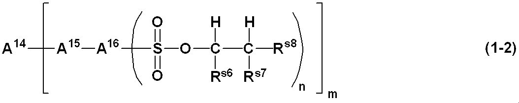
A14は、置換基を有していてもよい、1つ以上の芳香環を含むm価の炭化水素基であり、A15は、-O-又は-S-であり、A16は、(n+1)価の芳香族基であり;
m及びnは、前記と同じである。)

Rs14~Rs17は、それぞれ独立に、水素原子、又は直鎖状若しくは分岐状の炭素数1~20の1価脂肪族炭化水素基であり;
Rs18は、直鎖状若しくは分岐状の炭素数1~20の1価脂肪族炭化水素基、又は-ORs19であり、Rs19は、置換基を有していてもよい炭素数2~20の1価炭化水素基であり;
A17は、-O-、-S-又は-NH-であり;
A18は、(n+1)価の芳香族基であり;
nは、前記と同じである。)
6.前記3級アリールアミン化合物が、少なくとも2つの窒素原子を有し、かつ全ての窒素原子が3級アリールアミン構造を有するものである1~5のいずれかの電荷輸送性ワニス。
7.前記有機溶媒が、低極性有機溶媒である1~6のいずれかの電荷輸送性ワニス。
8.1~7のいずれかの電荷輸送性ワニスから得られる電荷輸送性薄膜。
9.8の電荷輸送性薄膜を備える有機EL素子。 Accordingly, the present invention provides the following charge transporting varnish.
1. Charge transport comprising (A) an aryl sulfonic acid ester compound, (B) a tertiary arylamine compound having at least one nitrogen atom, and all nitrogen atoms having a tertiary arylamine structure, and (C) an organic solvent Sex varnish.
2. 5. The charge transporting varnish according to 1, wherein the arylsulfonic acid ester compound is a fluorine atom-containing arylsulfonic acid ester compound.
3. The charge transporting varnish according to 1, wherein the arylsulfonic acid ester compound is represented by the following formula (1) or (1 ′).
A 2 is -O-, -S- or -NH-;
Or A 3 represents an (n + 1) -valent aromatic group having 6 to 20 carbon atoms;
X 1 is an alkylene group having 2 to 5 carbon atoms, and —O—, —S— or a carbonyl group may be interposed between carbon atoms of the alkylene group, and one of hydrogen atoms of the alkylene group is Part or all may be further substituted with an alkyl group having 1 to 20 carbon atoms;
X 2 is a single bond, -O-, -S- or -NR-, and R is a hydrogen atom or a monovalent hydrocarbon group having 1 to 10 carbon atoms;
X 3 represents a monovalent hydrocarbon group having 1 to 20 carbon atoms which may have a substituent;
m is an integer satisfying 1 ≦ m ≦ 4;
n is an integer satisfying 1 ≦ n ≦ 4. ]
4. A 1 is a fluorine atom-substituted m-valent hydrocarbon group having 6 to 20 carbon atoms including one or more aromatic rings, which is substituted by a fluorine atom, or m derived from the compound represented by the formula (2) or (3) Charge-transporting varnish of 3, which is a divalent group.
5. The charge transporting varnish according to any one of 1 to 4, wherein the arylsulfonic acid ester compound is represented by any one of the following formulas (1-1) to (1-3).
A 11 is an m-valent group derived from perfluorobiphenyl, A 12 is —O— or —S—, A 13 is a (n + 1) -valent group derived from naphthalene or anthracene Yes;
m and n are the same as above. )
A 14 is an m-valent hydrocarbon group containing one or more aromatic rings which may have a substituent, A 15 is —O— or —S—, and A 16 is n + 1) valent aromatic group;
m and n are the same as above. )
R s14 to R s17 are each independently a hydrogen atom or a linear or branched monovalent aliphatic hydrocarbon group having 1 to 20 carbon atoms;
R s18 is a linear or branched monovalent aliphatic hydrocarbon group having 1 to 20 carbon atoms, or -OR s19 , and R s19 has 2 to 20 carbon atoms which may have a substituent. A monovalent hydrocarbon group of
A 17 is -O-, -S- or -NH-;
A 18 is an (n + 1) -valent aromatic group;
n is the same as the above. )
6. 5. The charge transporting varnish according to any one of 1 to 5, wherein the tertiary arylamine compound has at least two nitrogen atoms, and all nitrogen atoms have a tertiary arylamine structure.
7. 6. The charge transporting varnish according to any one of 1 to 6, wherein the organic solvent is a low polar organic solvent.
A charge transporting thin film obtained from any one of the charge transporting varnishes according to 8.1 to 7.
The organic electroluminescent element provided with the charge transportable thin film of 9.8.
本発明の電荷輸送性ワニスは、(A)アリールスルホン酸エステル化合物、(B)少なくとも1つの窒素原子を有し、かつ全ての窒素原子が3級アリールアミン構造を有する3級アリールアミン化合物、及び(C)有機溶媒を含むものである。なお、本発明において電荷輸送性とは、導電性と同義であり、正孔輸送性とも同義である。また、本発明の電荷輸送性ワニスは、それ自体に電荷輸送性があるものでもよく、ワニスを使用して得られる固体膜に電荷輸送性があるものでもよい。 [Charge Transportable Varnish]
The charge transporting varnish of the present invention comprises (A) an arylsulfonic acid ester compound, (B) a tertiary arylamine compound having at least one nitrogen atom, and all nitrogen atoms having a tertiary arylamine structure, and (C) contains an organic solvent. In the present invention, charge transportability is synonymous with conductivity, and is also synonymous with hole transportability. Further, the charge transporting varnish of the present invention may be one having a charge transporting property per se, or may be one having a charge transporting property on a solid film obtained by using the varnish.
(A)成分のアリールスルホン酸エステル化合物は、電子受容性物質前駆体として機能するものである。なお、本発明において電子受容性物質とは、電子輸送能及び成膜均一性を向上させるために用いられるものである。前記アリールスルホン酸エステル化合物は、芳香環上にスルホン酸エステル基が結合したものであれば特に限定されない。 [(A) aryl sulfonic acid ester compound]
The arylsulfonic acid ester compound of component (A) functions as an electron accepting substance precursor. In the present invention, the electron accepting substance is used to improve the electron transporting ability and the film forming uniformity. The arylsulfonic acid ester compound is not particularly limited as long as it has an aromatic ring and a sulfonic acid ester group bonded thereto.
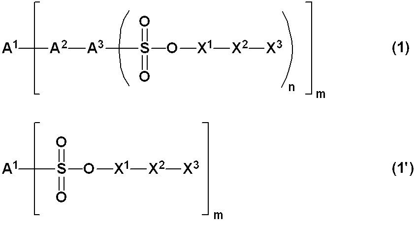
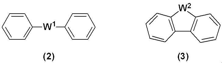
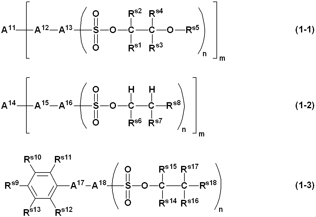
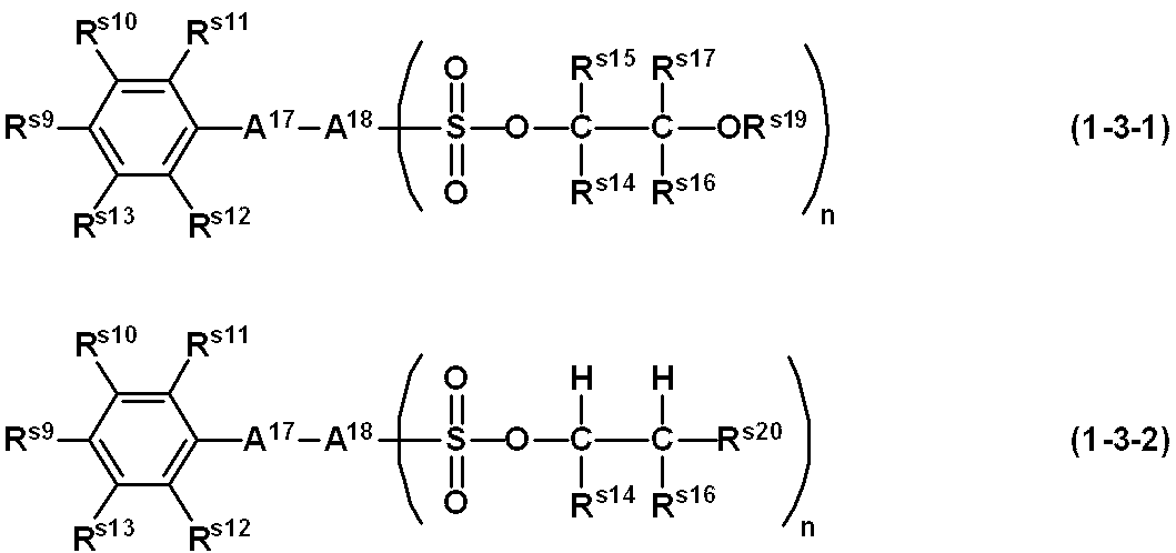

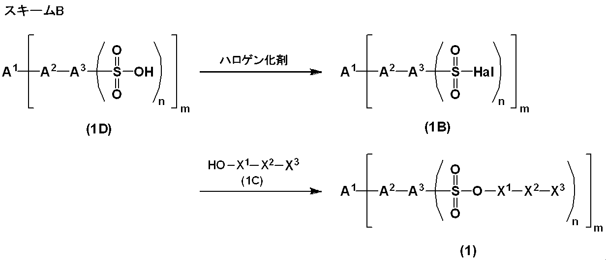
(B)成分の3級アリールアミン化合物は、少なくとも1つの窒素原子を有し、かつ全ての窒素原子が3級アリールアミン構造を有するものである。換言すれば、前記3級アリールアミン化合物は、少なくとも1つの窒素原子を有し、全ての窒素原子に3つの芳香族基が結合した構造を有するものである。前記3級アリールアミン化合物中、窒素原子は、2つ以上あることが好ましい。(B)成分の3級アリールアミン化合物は、電荷輸送性物質として機能する。 [(B) Tertiary arylamine compound]
The tertiary arylamine compound of component (B) is one having at least one nitrogen atom, and all nitrogen atoms have a tertiary arylamine structure. In other words, the tertiary arylamine compound has at least one nitrogen atom, and has a structure in which three aromatic groups are bonded to all nitrogen atoms. The number of nitrogen atoms in the tertiary arylamine compound is preferably two or more. The tertiary arylamine compound of component (B) functions as a charge transporting substance.


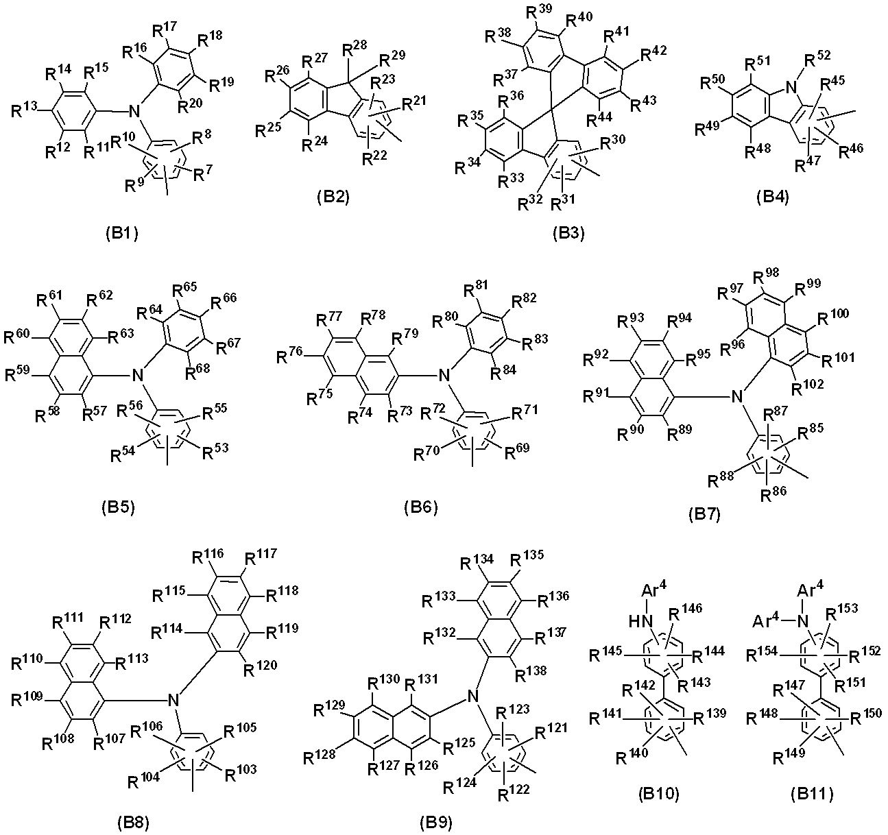
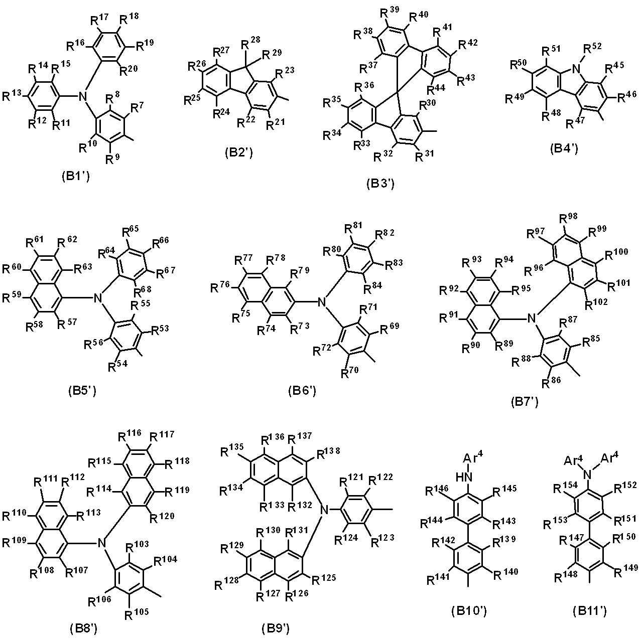


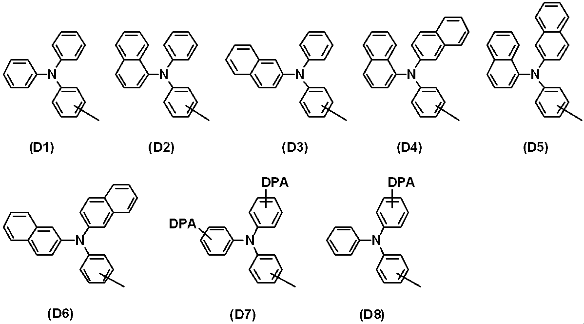

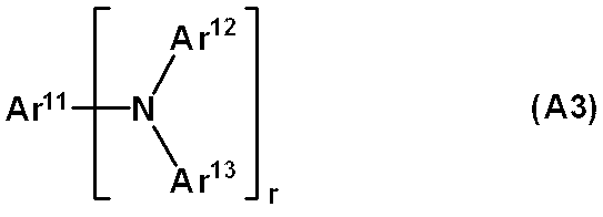

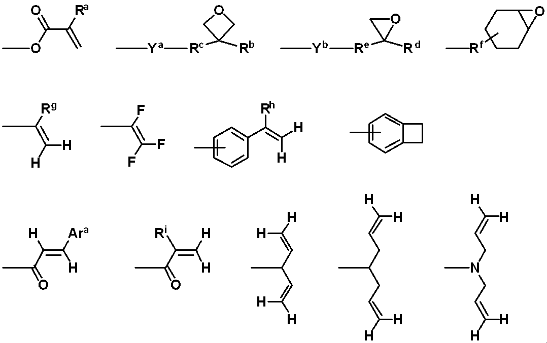

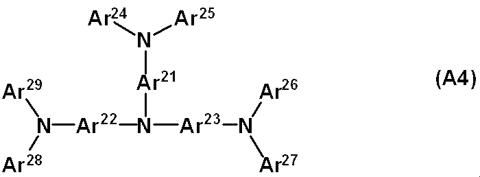

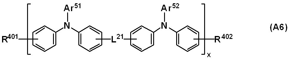
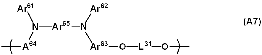
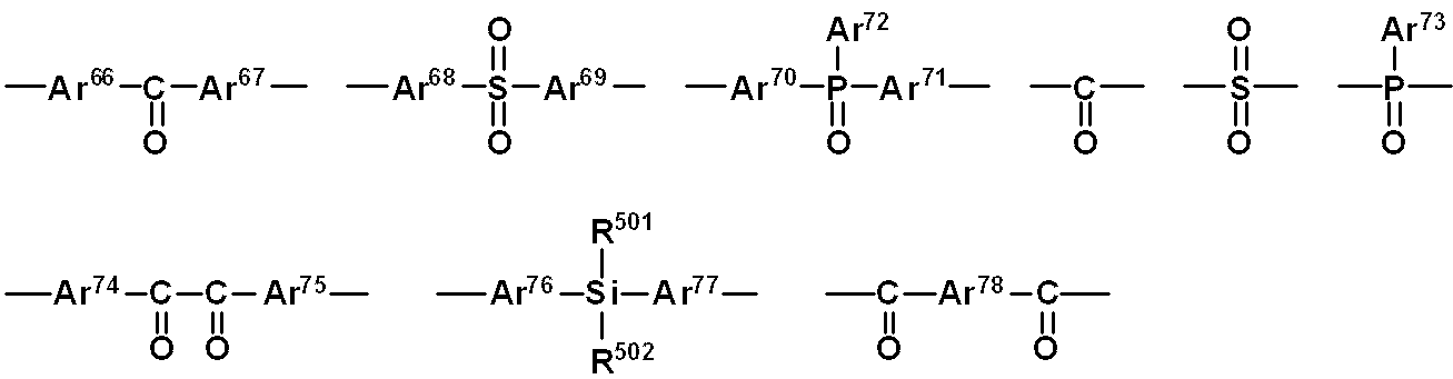

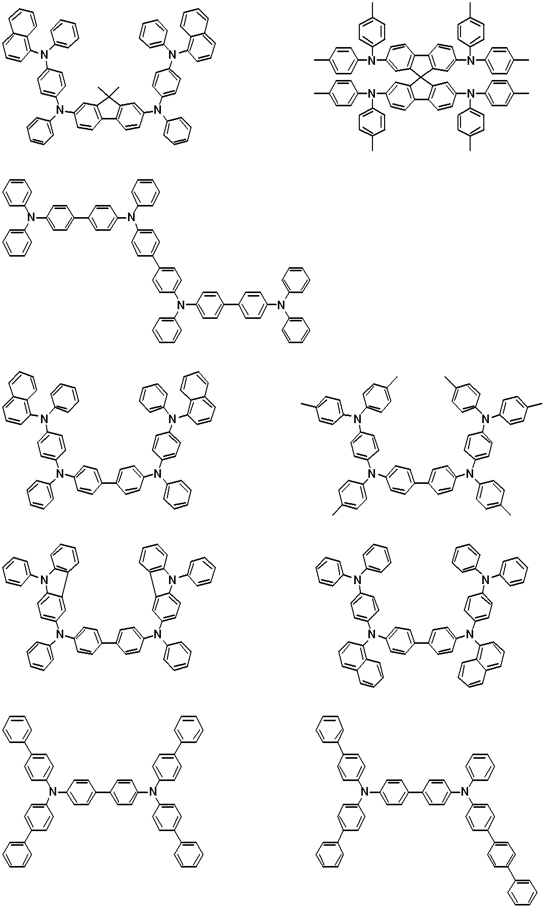

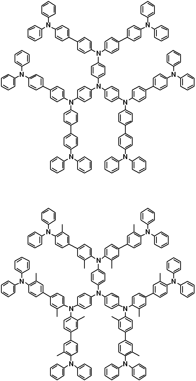
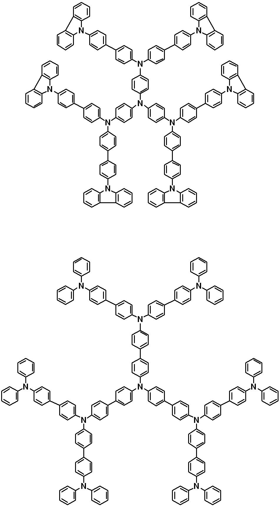
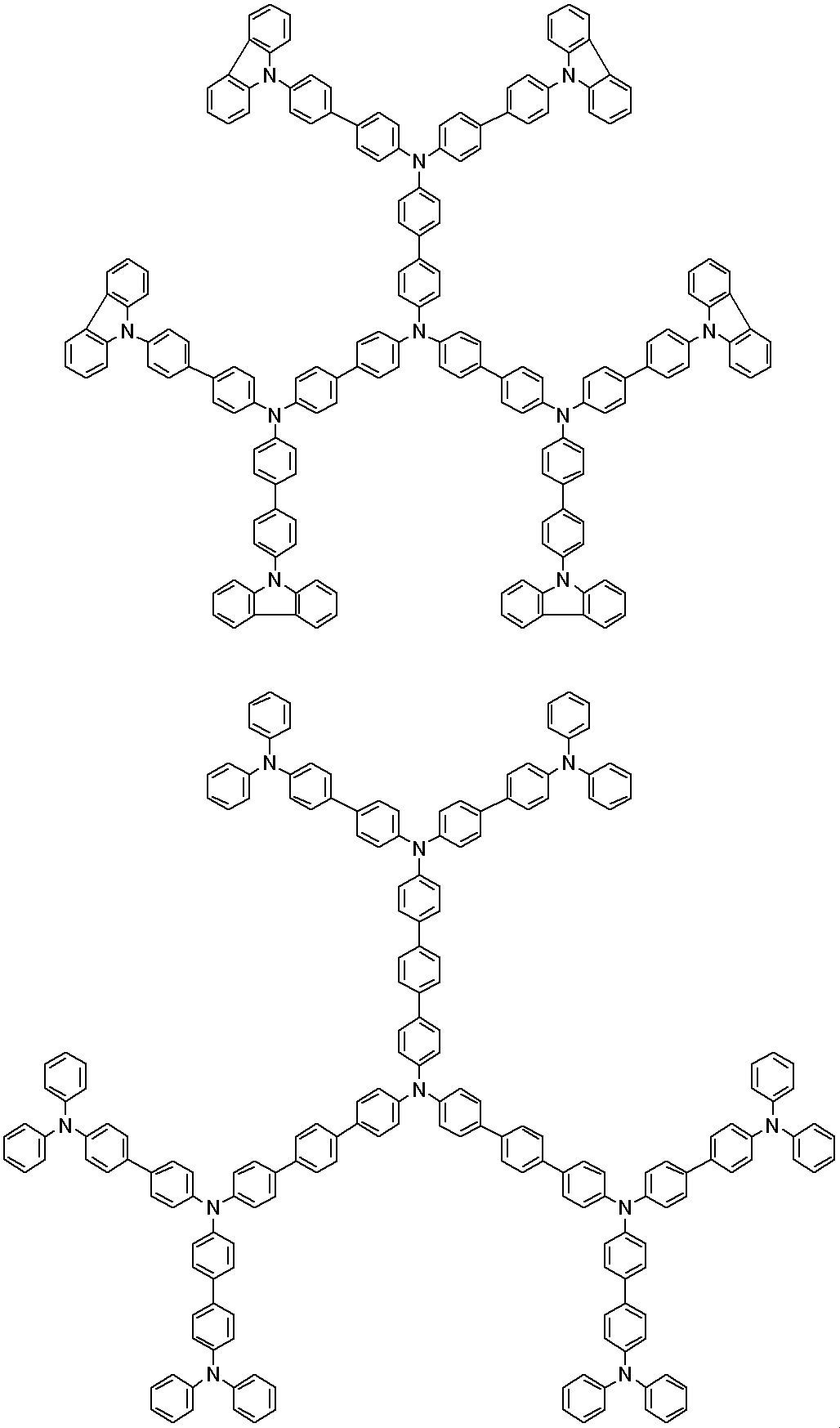


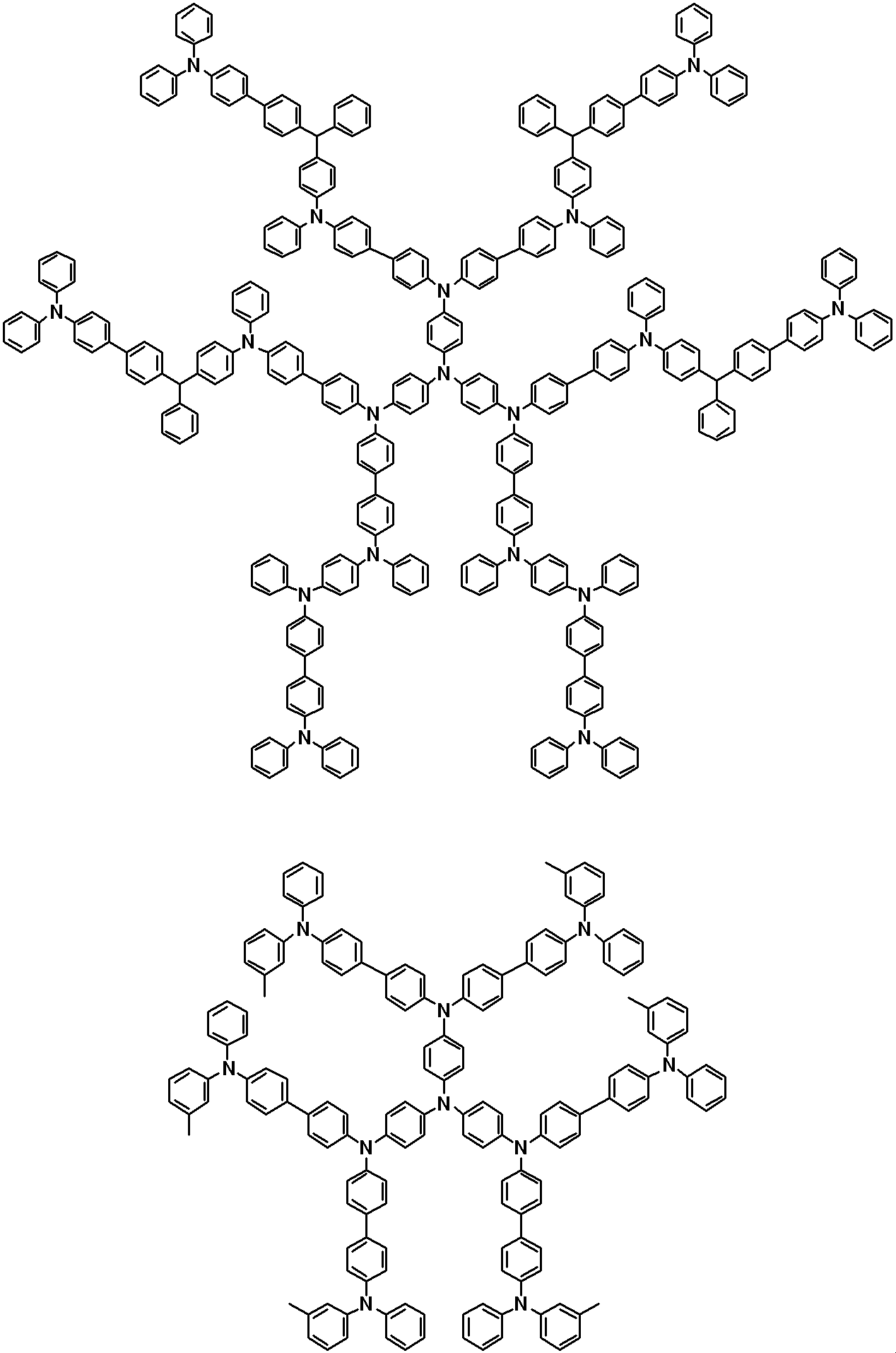


本発明の電荷輸送性ワニスを調製する際に用いられる有機溶媒としては、前記アリールスルホン酸エステル化合物及び前記3級アリールアミン化合物を良好に溶解し得る高溶解性溶媒を用いることができる。前記3級アリールアミン化合物を溶解させ、かつ非晶質な塗膜を得るためには、低極性溶媒を用いることが好ましい。エステル化されていないスルホン酸化合物を溶解させるためには、少なくとも1種の高極性溶媒を含有させることが必要であるのに対し、前記アリールスルホン酸エステル化合物は、溶媒の極性を問わず、溶媒中に溶解することが可能である。本発明において、低極性溶媒とは周波数100kHzでの比誘電率が7未満のものを、高極性溶媒とは周波数100kHzでの比誘電率が7以上のものと定義する。 [(C) organic solvent]
As the organic solvent used when preparing the charge transporting varnish of the present invention, a highly soluble solvent capable of satisfactorily dissolving the arylsulfonic acid ester compound and the tertiary arylamine compound can be used. In order to dissolve the tertiary arylamine compound and obtain an amorphous coating film, it is preferable to use a low polarity solvent. In order to dissolve the non-esterified sulfonic acid compound, it is necessary to contain at least one high polar solvent, while the arylsulfonic acid ester compound is a solvent regardless of the polarity of the solvent. It is possible to dissolve in. In the present invention, the low polar solvent is defined as one having a relative dielectric constant of less than 7 at a frequency of 100 kHz, and the high polar solvent is defined as one having a relative dielectric constant of 7 or more at a frequency of 100 kHz.
クロロホルム、クロロベンゼン等の塩素系溶媒;
トルエン、キシレン、テトラリン、シクロヘキシルベンゼン、デシルベンゼン等の芳香族炭化水素系溶媒、
1-オクタノール、1-ノナノール、1-デカノール等の脂肪族アルコール系溶媒;
テトラヒドロフラン、ジオキサン、アニソール、4-メトキシトルエン、3-フェノキシトルエン、ジベンジルエーテル、ジエチレングリコールジメチルエーテル、ジエチレングリコールブチルメチルエーテル、トリエチレングリコールジメチルエーテル、トリエチレングリコールブチルメチルエーテル等のエーテル系溶媒;
安息香酸メチル、安息香酸エチル、安息香酸ブチル、安息香酸イソアミル、フタル酸ビス(2-エチルヘキシル)、マレイン酸ジブチル、シュウ酸ジブチル、酢酸ヘキシル、ジエチレングリコールモノエチルエーテルアセテート、ジエチレングリコールモノブチルエーテルアセテート等のエステル系溶媒
等が挙げられる。 As a low polarity solvent, for example,
Chlorinated solvents such as chloroform and chlorobenzene;
Aromatic hydrocarbon solvents such as toluene, xylene, tetralin, cyclohexylbenzene and decylbenzene
Aliphatic alcohol solvents such as 1-octanol, 1-nonanol, 1-decanol;
Ether solvents such as tetrahydrofuran, dioxane, anisole, 4-methoxytoluene, 3-phenoxytoluene, dibenzyl ether, diethylene glycol dimethyl ether, diethylene glycol butyl methyl ether, triethylene glycol dimethyl ether, triethylene glycol butyl methyl ether;
Esters such as methyl benzoate, ethyl benzoate, butyl benzoate, isoamyl benzoate, bis (2-ethylhexyl) phthalate, dibutyl maleate, dibutyl oxalate, hexyl acetate, diethylene glycol monoethyl ether acetate, diethylene glycol monobutyl ether acetate Solvent etc. are mentioned.
N,N-ジメチルホルムアミド、N,N-ジメチルアセトアミド、N,N-ジメチルイソブチルアミド、N-メチルピロリドン、1,3-ジメチル-2-イミダゾリジノン等のアミド系溶媒;
エチルメチルケトン、イソホロン、シクロヘキサノン等のケトン系溶媒;
アセトニトリル、3-メトキシプロピオニトリル等のシアノ系溶媒;
エチレングリコール、ジエチレングリコール、トリエチレングリコール、ジプロピレングリコール、1,3-ブタンジオール、2,3-ブタンジオール等の多価アルコール系溶媒;
ジエチレングリコールモノメチルエーテル、ジエチレングリコールモノフェニルエーテル、トリエチレングリコールモノメチルエーテル、ジプロピレングリコールモノメチルエーテル、ベンジルアルコール、2-フェノキシエタノール、2-ベンジルオキシエタノール、3-フェノキシベンジルアルコール、テトラヒドロフルフリルアルコール等の脂肪族アルコール以外の1価アルコール系溶媒;
ジメチルスルホキシド等のスルホキシド系溶媒
等が挙げられる。 Moreover, as a high polar solvent, for example,
Amide solvents such as N, N-dimethylformamide, N, N-dimethylacetamide, N, N-dimethylisobutyramide, N-methylpyrrolidone, 1,3-dimethyl-2-imidazolidinone and the like;
Ketone solvents such as ethyl methyl ketone, isophorone, cyclohexanone;
Cyano solvents such as acetonitrile and 3-methoxypropionitrile;
Polyhydric alcohol solvents such as ethylene glycol, diethylene glycol, triethylene glycol, dipropylene glycol, 1,3-butanediol, 2,3-butanediol;
Other than aliphatic alcohols such as diethylene glycol monomethyl ether, diethylene glycol monophenyl ether, triethylene glycol monomethyl ether, dipropylene glycol monomethyl ether, benzyl alcohol, 2-phenoxyethanol, 2-benzyloxyethanol, 3-phenoxybenzyl alcohol, tetrahydrofurfuryl alcohol A monohydric alcohol solvent;
Sulfoxide solvents such as dimethyl sulfoxide and the like can be mentioned.
本発明の電荷輸送性ワニスを基材上に塗布して乾燥させることで、基材上に電荷輸送性薄膜を形成させることができる。 [Charge transportable thin film]
By applying the charge transporting varnish of the present invention on a substrate and drying it, a charge transporting thin film can be formed on the substrate.
本発明の有機EL素子は、一対の電極を有し、これら電極の間に、前述した本発明の電荷輸送性薄膜を備えるものである。 [Organic EL element]
The organic EL device of the present invention has a pair of electrodes, and the charge transporting thin film of the present invention described above is provided between these electrodes.
(a)陽極/正孔注入層/正孔輸送層/発光層/電子輸送層/電子注入層/陰極
(b)陽極/正孔注入層/正孔輸送層/発光層/電子注入輸送層/陰極
(c)陽極/正孔注入輸送層/発光層/電子輸送層/電子注入層/陰極
(d)陽極/正孔注入輸送層/発光層/電子注入輸送層/陰極
(e)陽極/正孔注入層/正孔輸送層/発光層/陰極
(f)陽極/正孔注入輸送層/発光層/陰極 Representative configurations of the organic EL element include the following (a) to (f), but are not limited thereto. In the following configuration, if necessary, an electron blocking layer or the like can be provided between the light emitting layer and the anode, and a hole blocking layer or the like can be provided between the light emitting layer and the cathode. In addition, the hole injection layer, the hole transport layer, or the hole injection transport layer may have a function as an electron block layer or the like, and the electron injection layer, the electron transport layer, or the electron injection transport layer may be a hole block layer or the like You may have the function as.
(A) anode / hole injection layer / hole transport layer / emission layer / electron transport layer / electron injection layer / cathode (b) anode / hole injection layer / hole transport layer / emission layer / electron injection transport layer / Cathode (c) anode / hole injection transport layer / light emitting layer / electron transport layer / electron injection layer / cathode (d) anode / hole injection transport layer / light emitting layer / electron injection transport layer / cathode (e) anode / positive Hole injection layer / hole transport layer / light emitting layer / cathode (f) anode / hole injection transport layer / light emitting layer / cathode
(1)1H-NMR、19F-NMR:JEOL(株)製、核磁気共鳴装置AL-300
(2)LC/MS:Waters社製、ZQ 2000
(3)基板洗浄:長州産業(株)製、基板洗浄装置(減圧プラズマ方式)
(4)ワニスの塗布:ミカサ(株)製、スピンコーターMS-A100
(5)膜厚測定:(株)小坂研究所製、微細形状測定機サーフコーダET-4000
(6)EL素子の作製:長州産業(株)製、多機能蒸着装置システムC-E2L1G1-N
(7)EL素子の輝度等の測定:(株)イーエッチシー製、多チャンネルIVL測定装置 Hereinafter, the present invention will be more specifically described by way of examples and comparative examples, but the present invention is not limited to the following examples. In the examples, devices used for preparation of samples and analysis of physical properties are as follows.
(1) 1 H-NMR, 19 F-NMR: manufactured by JEOL Ltd., nuclear magnetic resonance apparatus AL-300
(2) LC / MS: manufactured by Waters, ZQ 2000
(3) Substrate cleaning: manufactured by Choshu Sangyo Co., Ltd., substrate cleaning apparatus (reduced pressure plasma system)
(4) Coating of varnish: manufactured by Mikasa Co., Ltd., spin coater MS-A100
(5) Film thickness measurement: manufactured by Kosaka Laboratory Ltd., fine shape measuring apparatus Surf coder ET-4000
(6) Fabrication of EL element: Multifunctional deposition system C-E2L1G1-N manufactured by Choshu Sangyo Co., Ltd.
(7) Measurement of the luminance of the EL element, etc .: Multi-channel IVL measuring device manufactured by EHC Co., Ltd.
[合成例1-1]NSO-2-PGEEの合成-1
下記スキームに従って、アリールスルホン酸エステル化合物NSO-2-PGEEを合成した。
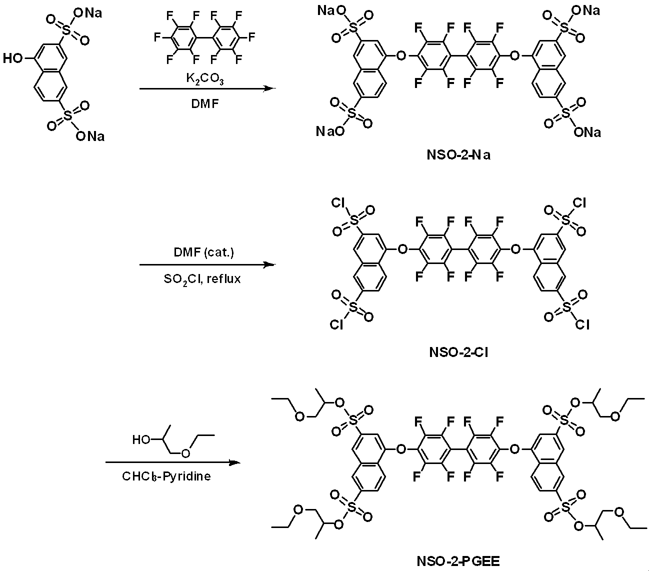
The arylsulfonic acid ester compound NSO-2-PGEE was synthesized according to the following scheme.
1H-NMR(500MHz, CDCl3): δ 0.92-0.97(m, 12H), 1.34 and 1.40(a pair of d, J=6.5Hz, 12H), 3.32-3.52(m, 16H), 4.80-4.87(m, 4H), 7.37(s, 2H), 8.22(d, J=8.5Hz, 2H), 8.45(s, 2H), 8.61(d, J=8.5Hz, 2H) , 8.69(s, 2H).
LC/MS (ESI+) m/z; 1264 [M+NH4]+ Chloroform (12 mL) and pyridine (8 mL) were added to the solid, and 2.50 g (24 mmol) of propylene glycol monoethyl ether (manufactured by Junsei Chemical Co., Ltd.) was added at 0 ° C. The temperature was raised to room temperature and then stirred for 3 hours. After evaporation of the solvent, water was added, extraction was performed with ethyl acetate, and the organic layer was dried over sodium sulfate. After filtration and concentration, the obtained crude product is purified by silica gel column chromatography (hexane / ethyl acetate) to obtain arylsulfonic acid ester compound NSO-2-PGEE (hereinafter referred to as NSO-2-PGEE-1). ) 1.09 g was obtained as a white solid (yield 44% (2 step yield from NSO-2-Na)). The measurement results of 1 H-NMR and LC / MS are shown below.
1 H-NMR (500 MHz, CDCl 3 ): δ 0.92-0.97 (m, 12 H), 1.34 and 1.40 (a pair of d, J = 6.5 Hz, 12 H), 3.32-3.52 (m, 16 H), 4.80-4.87 (m, 4 H), 7. 37 (s, 2 H), 8.22 (d, J = 8.5 Hz, 2 H), 8. 45 (s, 2 H), 8.61 (d, J = 8.5 Hz, 2 H), 8. 69 (s, 2 H) .
LC / MS (ESI + ) m / z; 1264 [M + NH 4 ] +
下記スキームに従ってスルホン酸エステル化合物NSO-2-PGEEを合成した。
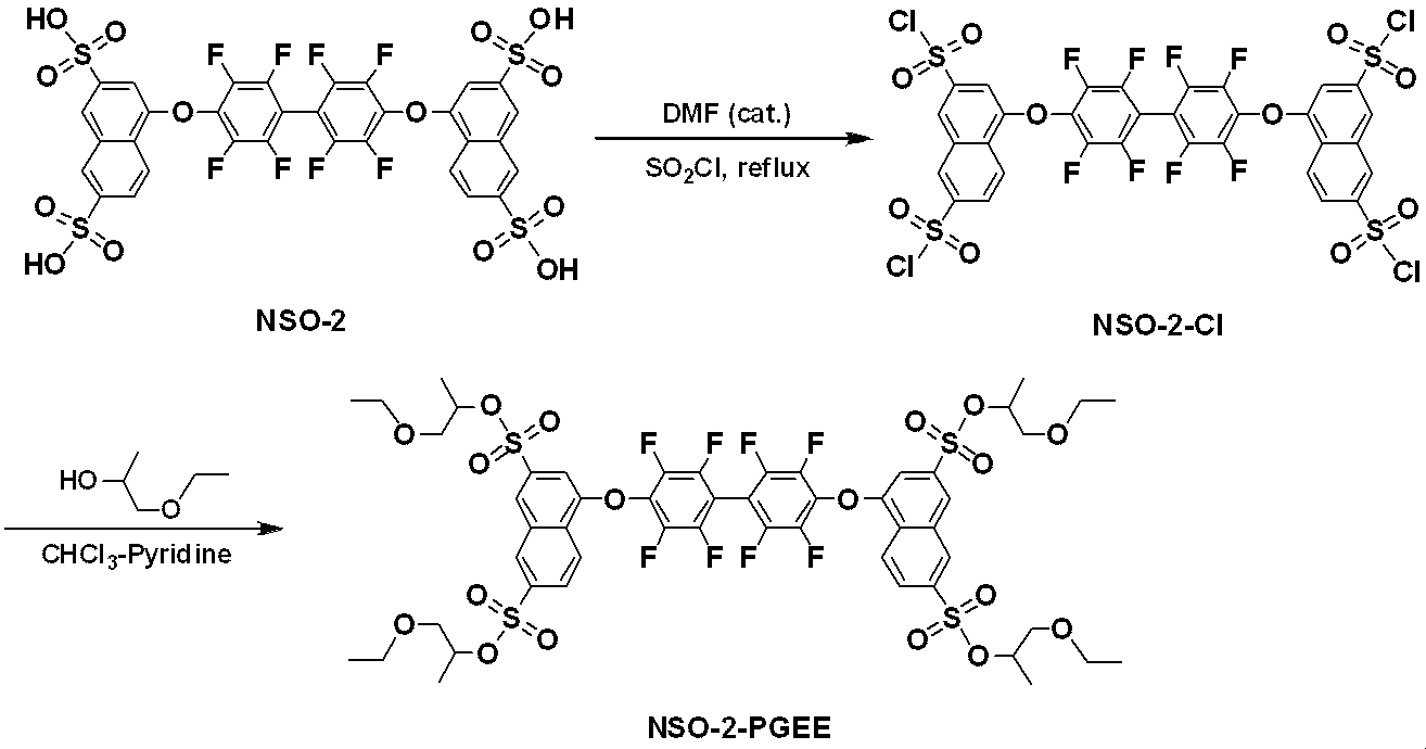
The sulfonic acid ester compound NSO-2-PGEE was synthesized according to the following scheme.
1H-NMR(500MHz, CDCl3): δ 0.92-0.97(m, 12H), 1.34 and 1.40(a pair of d, J=6.5Hz, 12H), 3.32-3.52(m, 16H), 4.80-4.87(m, 4H), 7.37(s, 2H), 8.22(d, J=8.5Hz, 2H), 8.45(s, 2H), 8.61(d, J=8.5Hz, 2H) , 8.69(s, 2H).
LC/MS (ESI+) m/z; 1264 [M+NH4]+ Thionyl chloride (8 mL) and DMF (85 μL) as a catalyst are added to 2 g (2.2 mmol) of NSO-2 synthesized according to the method described in WO 2006/025342, and after heating under reflux for 1 hour, thionyl chloride The solvent was distilled off to obtain a solid containing NSO-2-Cl. The compound was used in the next step without further purification. Chloroform (12 mL) and pyridine (8 mL) were added to the solid, and 2.75 g (26.4 mmol) of propylene glycol monoethyl ether (manufactured by Junsei Chemical Co., Ltd.) was added at 0 ° C. The temperature was raised to room temperature and then stirred for 3 hours. After evaporation of the solvent, water was added, extraction was performed with ethyl acetate, and the organic layer was dried over sodium sulfate. After filtration and concentration, the obtained crude product is purified by silica gel column chromatography (hexane / ethyl acetate) to obtain sulfonic acid ester compound NSO-2-PGEE (hereinafter referred to as NSO-2-PGEE-2). 1.50 g were obtained as a white solid (yield 54% (2 step yield from NSO-2)). The measurement results of 1 H-NMR and LC / MS are shown below.
1 H-NMR (500 MHz, CDCl 3 ): δ 0.92-0.97 (m, 12 H), 1.34 and 1.40 (a pair of d, J = 6.5 Hz, 12 H), 3.32-3.52 (m, 16 H), 4.80-4.87 (m, 4 H), 7. 37 (s, 2 H), 8.22 (d, J = 8.5 Hz, 2 H), 8. 45 (s, 2 H), 8.61 (d, J = 8.5 Hz, 2 H), 8. 69 (s, 2 H) .
LC / MS (ESI + ) m / z; 1264 [M + NH 4 ] +
下記スキームに従って、スルホン酸エステル化合物4FNS-4-PGEEを合成した。
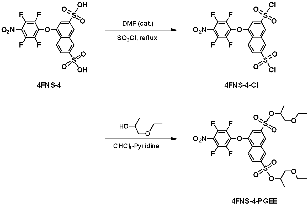
1H-NMR(500MHz, CDCl3): δ 0.89-0.95(m, 6H), 1.34 and 1.39(a pair of d, J=6.5Hz, 6H), 3.28-3.50(m, 8H), 4.81-4.87(m, 2H), 7.26(s, 1H), 8.22(d, J=9.0Hz, 1H), 8.47(s, 1H), 8.54(d, J=9.0Hz, 1H) , 8.68(s, 1H).
LC/MS (ESI+) m/z; 687 [M+NH4]+ Chloroform (30 mL) and pyridine (20 mL) were added to the solid, and 6.24 g (60 mmol) of propylene glycol monoethyl ether was added at 0 ° C. The temperature was raised to room temperature and then stirred for 1.5 hours. After evaporation of the solvent, water was added, extraction was performed with ethyl acetate, and the organic layer was dried over sodium sulfate. After filtration and concentration, the obtained crude product was purified by silica gel column chromatography (hexane / ethyl acetate) to obtain 1.32 g of sulfonic acid ester compound 4FNS-4-PGEE as a white solid (yield 20%) (2 step yield from 4 FNS-4)). The measurement results of 1 H-NMR and LC / MS are shown below.
1 H-NMR (500 MHz, CDCl 3 ): δ 0.89-0.95 (m, 6 H), 1.34 and 1. 39 (a pair of d, J = 6.5 Hz, 6 H), 3.28-3. 50 (m, 8 H), 4.81-4.87 (m, 2H), 7.26 (s, 1H), 8.22 (d, J = 9.0 Hz, 1 H), 8.47 (s, 1 H), 8.54 (d, J = 9.0 Hz, 1 H), 8.68 (s, 1 H) .
LC / MS (ESI + ) m / z; 687 [M + NH 4 ] +
[実施例1-1]
国際公開第2005/094133号記載の方法に従って合成した下記式(H1)で表される化合物H1(12.5mg)と、NSO-2-PGEE-1(12.5mg)との混合物に、クロロホルム(5g)を加えて室温で攪拌して溶解させ、得られた溶液を孔径0.2μmのシリンジフィルターでろ過して、電荷輸送性ワニスA1を得た。 [2] Preparation of Charge-Transporting Varnish [Example 1-1]
A mixture of a compound H1 (12.5 mg) represented by the following formula (H1) (12.5 mg) synthesized according to the method described in WO 2005/094133 and NSO-2-PGEE-1 (12.5 mg) 5 g) was added and stirred at room temperature to dissolve, and the resulting solution was filtered with a syringe filter with a pore size of 0.2 μm to obtain charge transporting varnish A1.
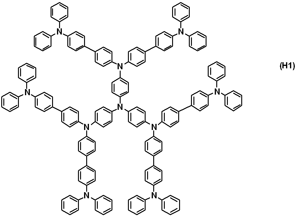
化合物H1(25mg)に、クロロホルム(5g)を加えて室温で攪拌して溶解させ、得られた溶液を孔径0.2μmのシリンジフィルターでろ過して、電荷輸送性ワニスA2を得た。 Comparative Example 1-1
Chloroform (5 g) was added to compound H1 (25 mg), and stirred at room temperature to dissolve, and the resulting solution was filtered with a syringe filter with a pore size of 0.2 μm to obtain charge transporting varnish A2.
国際公開第2013/098175号記載の方法に従って合成した下記式(H2)で表される化合物H2(12.5mg)と、NSO-2-PGEE-1(12.5mg)との混合物に、クロロホルム(5g)を加えて、室温で攪拌して溶解させ、得られた溶液を孔径0.2μmのシリンジフィルターでろ過して、電荷輸送性ワニスB1を得た。 Embodiment 1-2
A mixture of a compound H2 (12.5 mg) represented by the following formula (H2) synthesized according to the method described in WO 2013/098175 and NSO-2-PGEE-1 (12.5 mg) was chloroform ( 5 g) was added, and stirred at room temperature to dissolve, and the obtained solution was filtered with a syringe filter with a pore size of 0.2 μm to obtain charge transporting varnish B1.
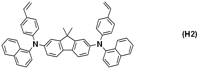
化合物H2(25mg)に、クロロホルム(5g)を加えて室温で攪拌して溶解させ、得られた溶液を孔径0.2μmのシリンジフィルターでろ過して、電荷輸送性ワニスB2を得た。 Comparative Example 1-2
Chloroform (5 g) was added to compound H2 (25 mg), and stirred at room temperature to dissolve, and the resulting solution was filtered with a syringe filter with a pore size of 0.2 μm to obtain charge transporting varnish B2.
下記式(H3)で表される化合物H3(TFBポリマー、Luminescence Technology社製LT-N148)(12.5mg)と、NSO-2-PGEE-1(12.5mg)との混合物に、クロロホルム(5g)を加えて室温で攪拌して溶解させ、得られた溶液を孔径0.2μmのシリンジフィルターでろ過して、電荷輸送性ワニスC1を得た。
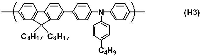
In a mixture of a compound H3 (TFB polymer, LT-N148 manufactured by Luminescence Technology) (12.5 mg) represented by the following formula (H3) and NSO-2-PGEE-1 (12.5 mg), chloroform (5 g) ) Was added and stirred at room temperature to dissolve, and the obtained solution was filtered with a syringe filter with a pore size of 0.2 μm to obtain a charge transporting varnish C1.
化合物H3(25mg)に、クロロホルム(5g)を加えて室温で攪拌して溶解させ、得られた溶液を孔径0.2μmのシリンジフィルターでろ過して、電荷輸送性ワニスC2を得た。 Comparative Example 1-3
Chloroform (5 g) was added to compound H3 (25 mg), and stirred at room temperature to dissolve, and the resulting solution was filtered with a syringe filter with a pore size of 0.2 μm to obtain charge transporting varnish C2.
化合物H1(12.5mg)と、NSO-2(12.5mg)との混合物に、クロロホルム(5g)を加えて、室温、350rpm、60分間攪拌したが、NSO-2は全く溶解しなかった。 Comparative Example 1-4
Chloroform (5 g) was added to a mixture of compound H1 (12.5 mg) and NSO-2 (12.5 mg), and stirred at room temperature at 350 rpm for 60 minutes, but NSO-2 did not dissolve at all.
化合物H2(12.5mg)と、NSO-2(12.5mg)との混合物に、クロロホルム(5g)を加えて、室温、350rpm、60分間攪拌したが、NSO-2は全く溶解しなかった。 Comparative Example 1-5
Chloroform (5 g) was added to a mixture of compound H2 (12.5 mg) and NSO-2 (12.5 mg) and stirred at room temperature at 350 rpm for 60 minutes, but NSO-2 did not dissolve at all.
化合物H3(12.5mg)と、NSO-2(12.5mg)との混合物に、クロロホルム(5g)を加えて、室温、350rpm、60分間攪拌したが、NSO-2は全く溶解しなかった。 Comparative Example 1-6
Chloroform (5 g) was added to a mixture of compound H3 (12.5 mg) and NSO-2 (12.5 mg), and stirred at room temperature at 350 rpm for 60 minutes, but NSO-2 did not dissolve at all.
国際公開第2015/050253号の合成例18に記載の方法に従って合成した下記式(H4)で表される化合物H4(190mg)、及びNSO-2-PGEE-2(337mg)を、3-フェノキシトルエン(5g)及びテトラリン(5g)の混合溶媒に加え、50℃、400rpm、5分間加熱攪拌した。これにより、NSO-2-PGEE-2は完全に溶媒に溶解した。得られた溶液を孔径0.2μmのPTFE製フィルターを用いて濾過し、電荷輸送性ワニスDを得た。

Compound H4 (190 mg) represented by the following formula (H4) synthesized according to the method described in Synthesis Example 18 of WO 2015/050253, and NSO-2-PGEE-2 (337 mg) It was added to a mixed solvent of (5 g) and tetralin (5 g), and heated and stirred at 50 ° C., 400 rpm for 5 minutes. Thereby, NSO-2-PGEE-2 was completely dissolved in the solvent. The resulting solution was filtered using a PTFE filter with a pore size of 0.2 μm to obtain a charge transporting varnish D.
化合物H4(48mg)、国際公開第2015/050253号の製造例24-2に記載の方法に従って合成した下記式(H5)で表される化合物H5(149mg)、及びNSO-2-PGEE-2(329mg)を、3-フェノキシトルエン(5g)及びテトラリン(5g)の混合溶媒に加え、50℃、400rpm、5分間加熱攪拌した。これにより、NSO-2-PGEE-2は完全に溶媒に溶解した。得られた溶液を孔径0.2μmのPTFE製フィルターを用いて濾過し、電荷輸送性ワニスEを得た。
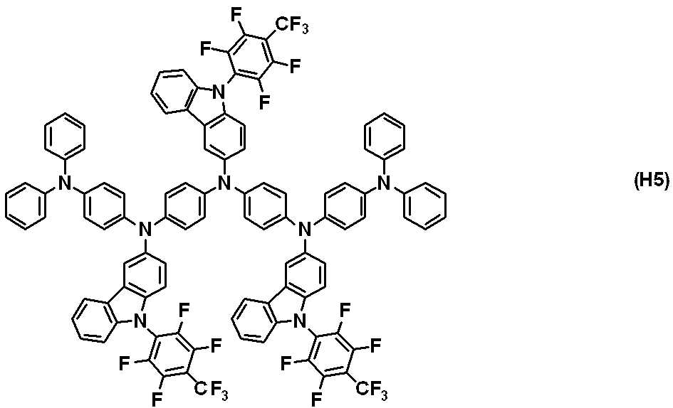
Compound H4 (48 mg), compound H5 (149 mg) represented by the following formula (H5) synthesized according to the method described in Production Example 24-2 of WO 2015/050253, and NSO-2-PGEE-2 ( 329 mg) was added to a mixed solvent of 3-phenoxytoluene (5 g) and tetralin (5 g), and heated and stirred at 50 ° C., 400 rpm for 5 minutes. Thereby, NSO-2-PGEE-2 was completely dissolved in the solvent. The resulting solution was filtered using a PTFE filter with a pore size of 0.2 μm to obtain charge transporting varnish E.
化合物H4(190mg)及びNSO-2-PGEE-2(337mg)を、トリエチレングリコールブチルメチルエーテル(7g)及び安息香酸ブチル(3g)の混合溶媒に加え、50℃、400rpm、5分間加熱攪拌した。これにより、NSO-2-PGEE-2は完全に溶媒に溶解した。得られた溶液を孔径0.2μmのPTFE製フィルターを用いて濾過し、電荷輸送性ワニスFを得た。 [Example 1-6]
Compound H4 (190 mg) and NSO-2-PGEE-2 (337 mg) were added to a mixed solvent of triethylene glycol butyl methyl ether (7 g) and butyl benzoate (3 g), and heated and stirred at 50 ° C., 400 rpm for 5 minutes . Thereby, NSO-2-PGEE-2 was completely dissolved in the solvent. The resulting solution was filtered using a PTFE filter with a pore size of 0.2 μm to obtain a charge transporting varnish F.
化合物H4(48mg)、化合物H5(149mg)及びNSO-2-PGEE-2(329mg)を、トリエチレングリコールブチルメチルエーテル(7g)及び安息香酸ブチル(3g)の混合溶媒に加え、50℃、400rpm、5分間加熱攪拌した。これにより、NSO-2-PGEE-2は完全に溶媒に溶解した。得られた溶液を孔径0.2μmのPTFE製フィルターを用いて濾過し、電荷輸送性ワニスGを得た。 [Example 1-7]
Compound H4 (48 mg), compound H5 (149 mg) and NSO-2-PGEE-2 (329 mg) are added to a mixed solvent of triethylene glycol butyl methyl ether (7 g) and butyl benzoate (3 g), 50 ° C., 400 rpm The mixture was heated and stirred for 5 minutes. Thereby, NSO-2-PGEE-2 was completely dissolved in the solvent. The resulting solution was filtered using a PTFE filter with a pore size of 0.2 μm to obtain a charge transporting varnish G.
化合物H4(190mg)及びNSO-2-PGEE-2(337mg)を、4-メトキシトルエン(7g)及びシクロヘキシルベンゼン(3g)の混合溶媒に加え、50℃、400rpm、5分間加熱攪拌した。これにより、NSO-2-PGEE-2は完全に溶媒に溶解した。得られた溶液を孔径0.2μmのPTFE製フィルターを用いて濾過し、電荷輸送性ワニスHを得た。 [Example 1-8]
Compound H4 (190 mg) and NSO-2-PGEE-2 (337 mg) were added to a mixed solvent of 4-methoxytoluene (7 g) and cyclohexylbenzene (3 g), and heated and stirred at 50 ° C., 400 rpm for 5 minutes. Thereby, NSO-2-PGEE-2 was completely dissolved in the solvent. The resulting solution was filtered using a PTFE filter with a pore size of 0.2 μm to obtain charge transporting varnish H.
化合物H4(48mg)、化合物H5(149mg)及びNSO-2-PGEE-2(329mg)を、4-メトキシトルエン(7g)及びシクロヘキシルベンゼン(3g)の混合溶媒に加え、5℃、400rpm、5分間加熱攪拌した。これにより、NSO-2-PGEE-2は完全に溶媒に溶解した。得られた溶液を孔径0.2μmのPTFE製フィルターを用いて濾過し、電荷輸送性ワニスIを得た。 [Example 1-9]
Compound H4 (48 mg), compound H5 (149 mg) and NSO-2-PGEE-2 (329 mg) are added to a mixed solvent of 4-methoxytoluene (7 g) and cyclohexylbenzene (3 g), and 5 ° C., 400 rpm, 5 minutes Heated and stirred. Thereby, NSO-2-PGEE-2 was completely dissolved in the solvent. The resulting solution was filtered using a PTFE filter having a pore size of 0.2 μm to obtain charge transporting varnish I.
化合物H4(190mg)及びNSO-2-PGEE-2(337mg)を、安息香酸エチル(7g)及びジベンジルエーテル(3g)の混合溶媒に加え、50℃、400rpm、5分間加熱攪拌した。これにより、NSO-2-PGEE-2は完全に溶媒に溶解した。得られた溶液を孔径0.2μmのPTFE製フィルターを用いて濾過し、電荷輸送性ワニスJを得た。 [Example 1-10]
Compound H4 (190 mg) and NSO-2-PGEE-2 (337 mg) were added to a mixed solvent of ethyl benzoate (7 g) and dibenzyl ether (3 g), and heated and stirred at 50 ° C., 400 rpm for 5 minutes. Thereby, NSO-2-PGEE-2 was completely dissolved in the solvent. The resulting solution was filtered using a PTFE filter with a pore size of 0.2 μm to obtain a charge transporting varnish J.
化合物H4(48mg)、化合物H5(149mg)及びNSO-2-PGEE-2(329mg)を、安息香酸エチル(7g)及びジベンジルエーテル(3g)の混合溶媒に加え、50℃、400rpm、5分間加熱攪拌した。これにより、NSO-2-PGEE-2は完全に溶媒に溶解した。得られた溶液を孔径0.2μmのPTFE製フィルターを用いて濾過し、電荷輸送性ワニスKを得た。 Example 1-11
Compound H4 (48 mg), compound H5 (149 mg) and NSO-2-PGEE-2 (329 mg) are added to a mixed solvent of ethyl benzoate (7 g) and dibenzyl ether (3 g), and 50 ° C., 400 rpm, 5 minutes Heated and stirred. Thereby, NSO-2-PGEE-2 was completely dissolved in the solvent. The resulting solution was filtered using a PTFE filter with a pore size of 0.2 μm to obtain a charge transporting varnish K.
化合物H4(270mg)及び4FNS-4-PGEE(257mg)を、3-フェノキシトルエン(3g)及び安息香酸ブチル(7g)の混合溶媒に加え、50℃、350rpm、10分間加熱攪拌した。これにより、4FNS-4-PGEEは完全に溶媒に溶解した。得られた溶液を孔径0.2μmのPTFE製フィルターを用いて濾過し、電荷輸送性ワニスLを得た。 Example 1-12
Compound H4 (270 mg) and 4FNS-4-PGEE (257 mg) were added to a mixed solvent of 3-phenoxytoluene (3 g) and butyl benzoate (7 g), and heated and stirred at 50 ° C., 350 rpm for 10 minutes. Thus, 4FNS-4-PGEE was completely dissolved in the solvent. The resulting solution was filtered using a PTFE filter with a pore size of 0.2 μm to obtain a charge transporting varnish L.
化合物H4(105mg)及び4FNS-4-PGEE(100mg)を、ジエチレングリコール(4g、比誘電率:25.2)及びトリエチレングリコールジメチルエーテル(6g、比誘電率:5.1)の混合溶媒に加え、50℃、350rpm、10分間加熱攪拌した。これにより、4FNS-4-PGEEは完全に溶媒に溶解した。得られた溶液を孔径0.2μmのPTFE製フィルターを用いて濾過し、電荷輸送性ワニスMを得た。 [Example 1-13]
Compound H4 (105 mg) and 4FNS-4-PGEE (100 mg) are added to a mixed solvent of diethylene glycol (4 g, dielectric constant: 25.2) and triethylene glycol dimethyl ether (6 g, dielectric constant: 5.1), The mixture was heated and stirred at 50 ° C. and 350 rpm for 10 minutes. Thus, 4FNS-4-PGEE was completely dissolved in the solvent. The resulting solution was filtered using a PTFE filter with a pore size of 0.2 μm to obtain a charge transporting varnish M.
化合物H4(120mg)及び4FNS-4(85mg)を、ジエチレングリコール(4g)及びトリエチレングリコールジメチルエーテル(6g)の混合溶媒に加え、50℃、350rpm、10分間加熱攪拌した。これにより、4FNS-4は完全に溶媒に溶解した。得られた溶液を孔径0.2μmのPTFE製フィルターを用いて濾過し、電荷輸送性ワニスNを得た。 Comparative Example 1-7
Compound H4 (120 mg) and 4FNS-4 (85 mg) were added to a mixed solvent of diethylene glycol (4 g) and triethylene glycol dimethyl ether (6 g), and heated and stirred at 50 ° C., 350 rpm for 10 minutes. Thus, 4FNS-4 completely dissolved in the solvent. The resulting solution was filtered using a PTFE filter with a pore size of 0.2 μm to obtain charge transporting varnish N.
化合物H3(25mg)と、p-トルエンスルホン酸メチル(東京化成工業(株)製)(38mg)との混合物に、クロロホルム(5g)を加えて室温で攪拌して溶解させ、得られた溶液を孔径0.2μmのシリンジフィルターでろ過して、電荷輸送性ワニスOを得た。 [Example 1-14]
Chloroform (5 g) is added to a mixture of compound H3 (25 mg) and methyl p-toluenesulfonic acid (manufactured by Tokyo Chemical Industry Co., Ltd.) (38 mg), stirred at room temperature to dissolve, and the obtained solution is The mixture was filtered with a syringe filter having a pore size of 0.2 μm to obtain a charge transporting varnish O.
化合物H3(25mg)と、ベンゼンスルホン酸エチル(東京化成工業(株)製)(38mg)との混合物に、クロロホルム(5g)を加えて室温で攪拌して溶解させ、得られた溶液を孔径0.2μmのシリンジフィルターでろ過して、電荷輸送性ワニスPを得た。 [Example 1-15]
Chloroform (5 g) is added to a mixture of compound H3 (25 mg) and ethyl benzene sulfonate (manufactured by Tokyo Chemical Industry Co., Ltd.) (38 mg), stirred at room temperature to dissolve, and the obtained solution has a pore size of 0 The mixture was filtered through a 2 μm syringe filter to obtain a charge transporting varnish P.
以下の実施例及び比較例において、ITO基板としては、ITOが表面上に膜厚150nmでパターニングされた25mm×25mm×0.7tのガラス基板を用い、使用前にO2プラズマ洗浄装置(150W、30秒間)によって表面上の不純物を除去したものを使用した。 [3] Single-Layer Device and Characteristic Evaluation In the following examples and comparative examples, a glass substrate of 25 mm × 25 mm × 0.7 t on which ITO is patterned with a film thickness of 150 nm is used as an ITO substrate The impurities on the surface were removed by an O 2 plasma cleaning device (150 W, 30 seconds).
電荷輸送性ワニスA1を、スピンコーターを用いてITO基板に塗布した後、大気下230℃で15分間焼成し、ITO基板上に60nmの薄膜を形成した。
その上に、蒸着装置(真空度2.0×10⁻⁵Pa)を用いてアルミニウムの薄膜を積層し、単層素子を得た。蒸着は、蒸着レート0.2nm/秒の条件で行った。アルミニウムの薄膜の膜厚は80nmとした。
なお、空気中の酸素、水等の影響による特性劣化を防止するため、単層素子は封止基板により封止した後、その特性を評価した。封止は、以下の手順で行った。
酸素濃度2ppm以下、露点-85℃以下の窒素雰囲気中で、単層素子を封止基板の間に収め、封止基板を接着材((株)MORESCO製モレスコモイスチャーカットWB90US(P))により貼り合わせた。この際、捕水剤(ダイニック(株)製HD-071010W-40)を単層素子と共に封止基板内に収めた。貼り合わせた封止基板に対し、紫外線を照射(波長365nm、照射量6,000mJ/cm2)した後、80℃で1時間、アニーリング処理して接着材を硬化させた。 Example 2-1
The charge transporting varnish A1 was applied to the ITO substrate using a spin coater, and then baked at 230 ° C. for 15 minutes in the atmosphere to form a 60 nm thin film on the ITO substrate.
A thin film of aluminum was laminated thereon using a vapor deposition apparatus (vacuum degree 2.0 × 10 −5 Pa) to obtain a single layer element. The deposition was performed under the conditions of a deposition rate of 0.2 nm / sec. The film thickness of the aluminum thin film was 80 nm.
In addition, in order to prevent the characteristic degradation due to the influence of oxygen in the air, water and the like, the single-layer device was sealed with a sealing substrate and then the characteristics were evaluated. Sealing was performed in the following procedure.
The single-layer element is housed between the sealing substrates in a nitrogen atmosphere with an oxygen concentration of 2 ppm or less and a dew point of -85 ° C. or less, and the sealing substrate is made of an adhesive (Moreless moist cut WB90US (P) manufactured by MORESCO) I stuck it. At this time, a water-capturing agent (HD-071010W-40, manufactured by Dynik Co., Ltd.) was placed in the sealing substrate together with the single layer element. The bonded sealing substrate was irradiated with ultraviolet light (wavelength 365 nm, irradiation amount 6,000 mJ / cm 2 ), and then annealed at 80 ° C. for 1 hour to cure the adhesive.
電荷輸送性ワニスA1のかわりに電荷輸送性ワニスA2を用いた以外は、実施例2-1と同様の方法で単層素子を作製した。 Comparative Example 2-1
A single layer device was produced in the same manner as in Example 2-1 except that the charge transporting varnish A2 was used instead of the charge transporting varnish A1.
電荷輸送性ワニスA1のかわりに電荷輸送性ワニスB1を用いた以外は、実施例2-1と同様の方法で単層素子を作製した。 Embodiment 2-2
A single layer device was produced in the same manner as in Example 2-1 except that the charge transporting varnish B1 was used instead of the charge transporting varnish A1.
電荷輸送性ワニスA1のかわりに電荷輸送性ワニスB2を用いた以外は、実施例2-1と同様の方法で単層素子を作製した。 Comparative Example 2-2
A single layer device was produced in the same manner as in Example 2-1 except that the charge transporting varnish B2 was used instead of the charge transporting varnish A1.
電荷輸送性ワニスA1のかわりに電荷輸送性ワニスC1を用いた以外は、実施例2-1と同様の方法で単層素子を作製した。 Example 2-3
A single layer device was produced in the same manner as in Example 2-1 except that the charge transporting varnish C1 was used instead of the charge transporting varnish A1.
電荷輸送性ワニスA1のかわりに電荷輸送性ワニスC2を用いた以外は、実施例2-1と同様の方法で単層素子を作製した。 Comparative Example 2-3
A single layer device was produced in the same manner as in Example 2-1 except that the charge transporting varnish C2 was used instead of the charge transporting varnish A1.

以下の実施例及び比較例において、ITO基板としては、前記と同様のものを使用した。 [4] Fabrication and characterization of hole-only device (HOD) -1
In the following examples and comparative examples, the same ones as described above were used as the ITO substrate.
電荷輸送性ワニスA1を、スピンコーターを用いてITO基板に塗布した後、大気下230℃で15分間焼成し、ITO基板上に60nmの薄膜を形成した。
その上に、蒸着装置(真空度2.0×10⁻⁵Pa)を用いてα-NPD及びアルミニウムの薄膜を順次積層し、HODを得た。蒸着は、蒸着レート0.2nm/秒の条件で行った。α-NPD及びアルミニウムの薄膜の膜厚は、それぞれ30nm及び80nmとした。
なお、空気中の酸素、水等の影響による特性劣化を防止するため、HODは封止基板により封止した後、その特性を評価した。封止は、以下の手順で行った。
酸素濃度2ppm以下、露点-85℃以下の窒素雰囲気中で、HODを封止基板の間に収め、封止基板を接着材((株)MORESCO製モレスコモイスチャーカットWB90US(P))により貼り合わせた。この際、捕水剤(ダイニック(株)製HD-071010W-40)をHODと共に封止基板内に収めた。貼り合わせた封止基板に対し、紫外線を照射(波長365nm、照射量6,000mJ/cm2)した後、80℃で1時間、アニーリング処理して接着材を硬化させた。 Example 3-1
The charge transporting varnish A1 was applied to the ITO substrate using a spin coater, and then baked at 230 ° C. for 15 minutes in the atmosphere to form a 60 nm thin film on the ITO substrate.
A thin film of α-NPD and aluminum was sequentially laminated thereon using a vapor deposition apparatus (vacuum degree 2.0 × 10 −5 Pa) to obtain a HOD. The deposition was performed under the conditions of a deposition rate of 0.2 nm / sec. The film thicknesses of the α-NPD and aluminum thin films were 30 nm and 80 nm, respectively.
In addition, in order to prevent the characteristic degradation by the influence of oxygen in the air, water, etc., the HOD was evaluated by the sealing substrate after sealing by the sealing substrate. Sealing was performed in the following procedure.
In a nitrogen atmosphere with an oxygen concentration of 2 ppm or less and a dew point of -85 ° C. or less, the HOD is contained between the sealing substrate, and the sealing substrate is bonded with an adhesive (MORE COS CORP The At this time, a water-capturing agent (HD-071010W-40, manufactured by Dynik Co., Ltd.) was placed in the sealing substrate together with the HOD. The bonded sealing substrate was irradiated with ultraviolet light (wavelength 365 nm, irradiation amount 6,000 mJ / cm 2 ), and then annealed at 80 ° C. for 1 hour to cure the adhesive.
電荷輸送性ワニスA1のかわりに電荷輸送性ワニスA2を用いた以外は、実施例3-1と同様の方法でHODを作製した。 Comparative Example 3-1
A HOD was produced in the same manner as in Example 3-1 except that the charge transporting varnish A2 was used instead of the charge transporting varnish A1.
電荷輸送性ワニスA1のかわりに電荷輸送性ワニスB1を用いた以外は、実施例3-1と同様の方法でHODを作製した。 Example 3-2
A HOD was produced in the same manner as in Example 3-1 except that the charge transporting varnish B1 was used instead of the charge transporting varnish A1.
電荷輸送性ワニスA1のかわりに電荷輸送性ワニスB2を用いた以外は、実施例3-1と同様の方法でHODを作製した。 Comparative Example 3-2
A HOD was produced in the same manner as in Example 3-1 except that the charge transporting varnish B2 was used instead of the charge transporting varnish A1.
電荷輸送性ワニスA1のかわりに電荷輸送性ワニスC1を用いた以外は、実施例3-1と同様の方法でHODを作製した。 Embodiment 3-3
A HOD was produced in the same manner as in Example 3-1 except that the charge transporting varnish C1 was used instead of the charge transporting varnish A1.
電荷輸送性ワニスA1のかわりに電荷輸送性ワニスC2を用いた以外は、実施例3-1と同様の方法でHODを作製した。 Comparative Example 3-3
A HOD was produced in the same manner as in Example 3-1 except that the charge transporting varnish C2 was used instead of the charge transporting varnish A1.
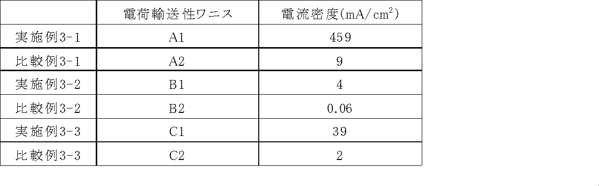
以下の実施例及び比較例において、ITO基板としては、前記と同様のものを使用した。 [5] Production and characterization of HOD-2
In the following examples and comparative examples, the same ones as described above were used as the ITO substrate.
電荷輸送性ワニスDを、スピンコーターを用いてITO基板に塗布した後、大気下で、120℃で1分間仮焼成をし、次いで230℃で15分間本焼成をし、ITO基板上に30nmの正孔注入層薄膜を形成した。
次に、窒素雰囲気のグローブボックス内で、TFBポリマー(Luminescence Technology社製LT-N148)の0.6質量%キシレン溶液を正孔注入層上にスピンコートにより成膜し、130℃で10分間の加熱焼成を行い、40nmの正孔輸送層薄膜を形成した。
その上に、蒸着装置(真空度2.0×10⁻⁵Pa)を用いてアルミニウムの薄膜を積層し、HODを得た。蒸着は、蒸着レート0.2nm/秒の条件で行った。アルミニウムの薄膜の膜厚は、80nmとした。
なお、空気中の酸素、水等の影響による特性劣化を防止するため、HODは封止基板により封止した後、その特性を評価した。封止は、以下の手順で行った。
酸素濃度2ppm以下、露点-85℃以下の窒素雰囲気中で、HODを封止基板の間に収め、封止基板を接着材((株)MORESCO製モレスコモイスチャーカットWB90US(P))により貼り合わせた。この際、捕水剤(ダイニック(株)製HD-071010W-40)をHODと共に封止基板内に収めた。貼り合わせた封止基板に対し、紫外線を照射(波長365nm、照射量6,000mJ/cm2)した後、80℃で1時間、アニーリング処理して接着材を硬化させた。 Example 4-1
The charge transport varnish D is applied to the ITO substrate using a spin coater, and then pre-baked at 120 ° C. for 1 minute in the atmosphere, followed by main baking at 230 ° C. for 15 minutes, and 30 nm on the ITO substrate. A hole injection layer thin film was formed.
Next, a 0.6 mass% xylene solution of TFB polymer (LT-N148 manufactured by Luminescence Technology) is spin-coated on the hole injection layer in a glove box under a nitrogen atmosphere, and the film is formed at 130 ° C. for 10 minutes. Heating and baking were performed to form a 40 nm hole transport layer thin film.
A thin film of aluminum was laminated thereon using a vapor deposition apparatus (vacuum degree 2.0 × 10 −5 Pa) to obtain a HOD. The deposition was performed under the conditions of a deposition rate of 0.2 nm / sec. The film thickness of the aluminum thin film was 80 nm.
In addition, in order to prevent the characteristic degradation by the influence of oxygen in the air, water, etc., the HOD was evaluated by the sealing substrate after sealing by the sealing substrate. Sealing was performed in the following procedure.
In a nitrogen atmosphere with an oxygen concentration of 2 ppm or less and a dew point of -85 ° C. or less, the HOD is contained between the sealing substrate, and the sealing substrate is bonded with an adhesive (MORE COS CORP The At this time, a water-capturing agent (HD-071010W-40, manufactured by Dynik Co., Ltd.) was placed in the sealing substrate together with the HOD. The bonded sealing substrate was irradiated with ultraviolet light (wavelength 365 nm, irradiation amount 6,000 mJ / cm 2 ), and then annealed at 80 ° C. for 1 hour to cure the adhesive.
電荷輸送性ワニスDのかわりに電荷輸送性ワニスEを用いた以外は、実施例4-1と同様の方法でHODを作製した。 Embodiment 4-2
A HOD was produced in the same manner as in Example 4-1 except that the charge transporting varnish E was used instead of the charge transporting varnish D.
電荷輸送性ワニスDのかわりに電荷輸送性ワニスFを用いた以外は、実施例4-1と同様の方法でHODを作製した。 Example 4-3
A HOD was produced in the same manner as in Example 4-1 except that the charge transporting varnish F was used instead of the charge transporting varnish D.
電荷輸送性ワニスDのかわりに電荷輸送性ワニスGを用いた以外は、実施例4-1と同様の方法でHODを作製した。 Example 4-4
A HOD was produced in the same manner as in Example 4-1 except that the charge transporting varnish G was used instead of the charge transporting varnish D.
電荷輸送性ワニスDのかわりに電荷輸送性ワニスHを用いた以外は、実施例4-1と同様の方法でHODを作製した。 Example 4-5
A HOD was produced in the same manner as in Example 4-1 except that the charge transporting varnish H was used instead of the charge transporting varnish D.
電荷輸送性ワニスDのかわりに電荷輸送性ワニスIを用いた以外は、実施例4-1と同様の方法でHODを作製した。 Embodiment 4-6
A HOD was produced in the same manner as in Example 4-1 except that the charge transporting varnish I was used instead of the charge transporting varnish D.
電荷輸送性ワニスDのかわりに電荷輸送性ワニスJを用いた以外は、実施例4-1と同様の方法でHODを作製した。 [Example 4-7]
A HOD was produced in the same manner as in Example 4-1 except that the charge transporting varnish J was used instead of the charge transporting varnish D.
電荷輸送性ワニスDのかわりに電荷輸送性ワニスKを用いた以外は、実施例4-1と同様の方法でHODを作製した。 [Example 4-8]
A HOD was produced in the same manner as in Example 4-1 except that the charge transporting varnish K was used instead of the charge transporting varnish D.
正孔注入層を形成しなかったこと以外は、実施例4-1と同様の方法でHODを作製した。 Comparative Example 4-1
An HOD was produced in the same manner as in Example 4-1 except that the hole injection layer was not formed.

以下の実施例及び比較例において、ITO基板としては、前記と同様のものを使用した。 [6] Preparation and characterization of HOD-3
In the following examples and comparative examples, the same ones as described above were used as the ITO substrate.
電荷輸送性ワニスLを、スピンコーターを用いてITO基板に塗布した後、大気下で、120℃で1分間仮焼成をし、次いで230℃で15分間本焼成をし、ITO基板上に40nmの薄膜を形成した。
その上に、蒸着装置(真空度2.0×10⁻⁵Pa)を用いてα-NPD及びアルミニウムの薄膜を順次積層し、HODを得た。蒸着は、蒸着レート0.2nm/秒の条件で行った。α-NPD及びアルミニウムの薄膜の膜厚は、それぞれ30nm及び80nmとした。
なお、空気中の酸素、水等の影響による特性劣化を防止するため、HODは封止基板により封止した後、その特性を評価した。封止は、以下の手順で行った。
酸素濃度2ppm以下、露点-85℃以下の窒素雰囲気中で、HODを封止基板の間に収め、封止基板を接着材((株)MORESCO製モレスコモイスチャーカットWB90US(P))により貼り合わせた。この際、捕水剤(ダイニック(株)製HD-071010W-40)をHODと共に封止基板内に収めた。貼り合わせた封止基板に対し、紫外線を照射(波長365nm、照射量6,000mJ/cm2)した後、80℃で1時間、アニーリング処理して接着材を硬化させた。 Example 5-1
The charge transport varnish L is applied to an ITO substrate using a spin coater, and then temporary baking is performed at 120 ° C. for 1 minute in the atmosphere, and then main baking is performed at 230 ° C. for 15 minutes. A thin film was formed.
A thin film of α-NPD and aluminum was sequentially laminated thereon using a vapor deposition apparatus (vacuum degree 2.0 × 10 −5 Pa) to obtain a HOD. The deposition was performed under the conditions of a deposition rate of 0.2 nm / sec. The film thicknesses of the α-NPD and aluminum thin films were 30 nm and 80 nm, respectively.
In addition, in order to prevent the characteristic degradation by the influence of oxygen in the air, water, etc., the HOD was evaluated by the sealing substrate after sealing by the sealing substrate. Sealing was performed in the following procedure.
In a nitrogen atmosphere with an oxygen concentration of 2 ppm or less and a dew point of -85 ° C. or less, the HOD is contained between the sealing substrate, and the sealing substrate is bonded with an adhesive (MORE COS CORP The At this time, a water-capturing agent (HD-071010W-40, manufactured by Dynik Co., Ltd.) was placed in the sealing substrate together with the HOD. The bonded sealing substrate was irradiated with ultraviolet light (wavelength 365 nm, irradiation amount 6,000 mJ / cm 2 ), and then annealed at 80 ° C. for 1 hour to cure the adhesive.
電荷輸送性ワニスLのかわりに電荷輸送性ワニスMを用いた以外は、実施例5-1と同様の方法でHODを作製した。 Example 5-2
A HOD was produced in the same manner as in Example 5-1 except that the charge transporting varnish M was used instead of the charge transporting varnish L.
電荷輸送性ワニスLのかわりに電荷輸送性ワニスNを用いた以外は、実施例5-1と同様の方法でHODを作製した。 Comparative Example 5-1
A HOD was produced in the same manner as in Example 5-1 except that the charge transporting varnish N was used instead of the charge transporting varnish L.

[実施例6-1]
電荷輸送性ワニスA1を、スピンコーターを用いてITO基板に塗布した後、大気下230℃で15分間焼成し、ITO基板上に60nmの薄膜を形成した。
その上に、蒸着装置(真空度2.0×10⁻⁵Pa)を用いてα-NPD 30nm、Alq3 40nmを、順次積層した。この際の蒸着レートは、0.2nm/秒とした。次いで、フッ化リチウム及びアルミニウムの薄膜を順次積層して有機EL素子を得た。この際、蒸着レートは、フッ化リチウムについては0.02nm/秒、アルミニウムについては0.2nm/秒とした。フッ化リチウム及びアルミニウムの薄膜の膜厚は、それぞれ0.5nm及び80nmとした。
なお、空気中の酸素、水等の影響による特性劣化を防止するため、有機EL素子は封止基板により封止した後、その特性を評価した。封止は、以下の手順で行った。
酸素濃度2ppm以下、露点-85℃以下の窒素雰囲気中で、有機EL素子を封止基板の間に収め、封止基板を接着材((株)MORESCO製モレスコモイスチャーカットWB90US(P))により貼り合わせた。この際、捕水剤(ダイニック(株)製HD-071010W-40)を有機EL素子と共に封止基板内に収めた。貼り合わせた封止基板に対し、紫外線を照射(波長365nm、照射量6,000mJ/cm2)した後、80℃で1時間、アニーリング処理して接着材を硬化させた。 [7] Preparation of organic EL element and characteristic evaluation [Example 6-1]
The charge transporting varnish A1 was applied to the ITO substrate using a spin coater, and then baked at 230 ° C. for 15 minutes in the atmosphere to form a 60 nm thin film on the ITO substrate.
On that, α-NPD 30 nm and Alq 3 40 nm were sequentially laminated using a vapor deposition apparatus (vacuum degree 2.0 × 10 −5 Pa). The deposition rate at this time was 0.2 nm / second. Subsequently, thin films of lithium fluoride and aluminum were sequentially laminated to obtain an organic EL element. At this time, the deposition rate was 0.02 nm / second for lithium fluoride and 0.2 nm / second for aluminum. The film thicknesses of the lithium fluoride and aluminum thin films were 0.5 nm and 80 nm, respectively.
In addition, in order to prevent the characteristic degradation by the influence of oxygen in the air, water, etc., after sealing the organic EL element with a sealing substrate, the characteristic was evaluated. Sealing was performed in the following procedure.
The organic EL element is housed between the sealing substrate in a nitrogen atmosphere with an oxygen concentration of 2 ppm or less and a dew point of -85 ° C. or less, and the sealing substrate is made of an adhesive (Moreless Co., Ltd. Moresco Cut WB90 US (P) manufactured by MORESCO) I stuck it. At this time, a water-capturing agent (HD-071010W-40, manufactured by Dynik Co., Ltd.) was placed in the sealing substrate together with the organic EL element. The bonded sealing substrate was irradiated with ultraviolet light (wavelength 365 nm, irradiation amount 6,000 mJ / cm 2 ), and then annealed at 80 ° C. for 1 hour to cure the adhesive.
電荷輸送性ワニスA1のかわりに電荷輸送性ワニスA2を用いた以外は、実施例6-1と同様の方法で有機EL素子を作製した。 Comparative Example 6-1
An organic EL device was produced in the same manner as in Example 6-1 except that the charge transporting varnish A2 was used instead of the charge transporting varnish A1.
電荷輸送性ワニスA1のかわりに電荷輸送性ワニスB1を用いた以外は、実施例6-1と同様の方法で有機EL素子を作製した。 Example 6-2
An organic EL device was produced in the same manner as in Example 6-1 except that the charge transporting varnish B1 was used instead of the charge transporting varnish A1.
電荷輸送性ワニスA1のかわりに電荷輸送性ワニスB2を用いた以外は、実施例6-1と同様の方法で有機EL素子を作製した。 Comparative Example 6-2
An organic EL device was produced in the same manner as in Example 6-1 except that the charge transporting varnish B2 was used instead of the charge transporting varnish A1.
電荷輸送性ワニスA1のかわりに電荷輸送性ワニスC1を用いた以外は、実施例6-1と同様の方法で有機EL素子を作製した。 Example 6-3
An organic EL device was produced in the same manner as in Example 6-1 except that the charge transporting varnish C1 was used instead of the charge transporting varnish A1.
電荷輸送性ワニスA1のかわりに電荷輸送性ワニスOを用いた以外は、実施例6-1と同様の方法で有機EL素子を作製した。 Example 6-4
An organic EL device was produced in the same manner as in Example 6-1 except that the charge transporting varnish O was used instead of the charge transporting varnish A1.
電荷輸送性ワニスA1のかわりに電荷輸送性ワニスPを用いた以外は、実施例6-1と同様の方法で有機EL素子を作製した。 [Example 6-5]
An organic EL device was produced in the same manner as in Example 6-1 except that the charge transporting varnish P was used instead of the charge transporting varnish A1.
電荷輸送性ワニスA1のかわりに電荷輸送性ワニスC2を用いた以外は、実施例6-1と同様の方法で有機EL素子を作製した。 Comparative Example 6-3
An organic EL device was produced in the same manner as in Example 6-1 except that the charge transporting varnish C2 was used instead of the charge transporting varnish A1.
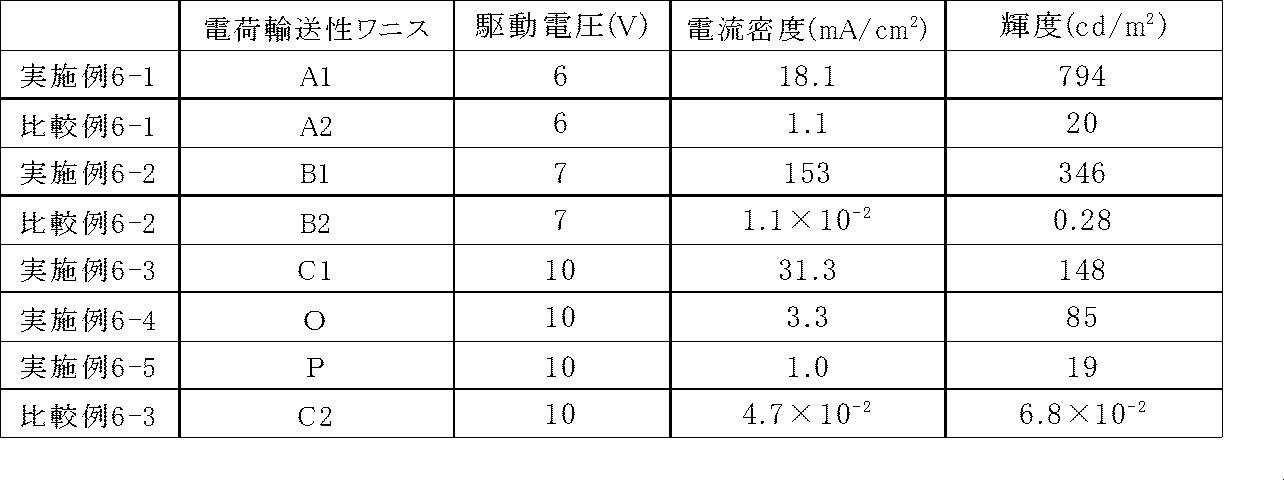
Claims (9)
- (A)アリールスルホン酸エステル化合物、(B)少なくとも1つの窒素原子を有し、かつ全ての窒素原子が3級アリールアミン構造を有する3級アリールアミン化合物、及び(C)有機溶媒を含む電荷輸送性ワニス。 Charge transport comprising (A) an aryl sulfonic acid ester compound, (B) a tertiary arylamine compound having at least one nitrogen atom, and all nitrogen atoms having a tertiary arylamine structure, and (C) an organic solvent Sex varnish.
- 前記アリールスルホン酸エステル化合物が、フッ素原子含有アリールスルホン酸エステル化合物である請求項1記載の電荷輸送性ワニス。 The charge transporting varnish according to claim 1, wherein the arylsulfonic acid ester compound is a fluorine atom-containing arylsulfonic acid ester compound.
- 前記アリールスルホン酸エステル化合物が、下記式(1)又は(1')で表されるものである請求項1記載の電荷輸送性ワニス。
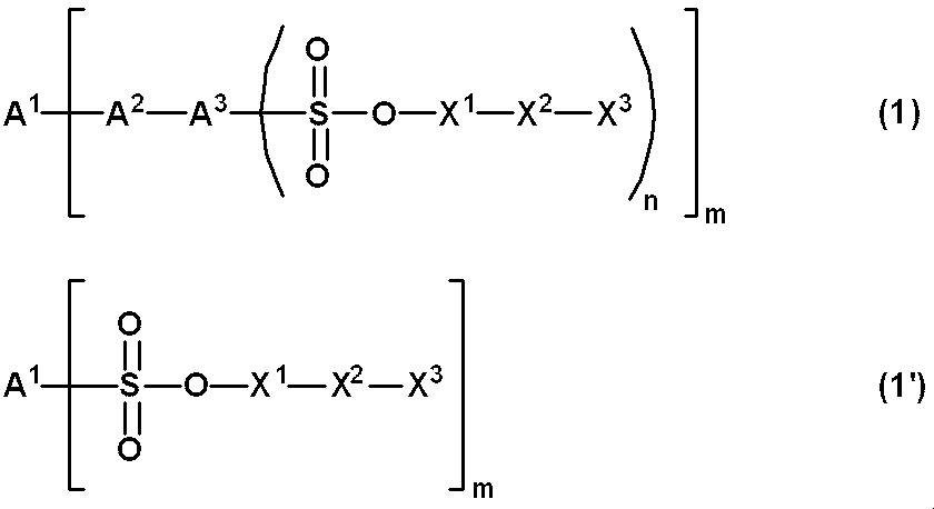
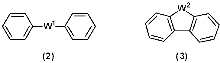
A2は、-O-、-S-又は-NH-であり;
A3は、又は炭素数6~20の(n+1)価の芳香族基であり;
X1は、炭素数2~5のアルキレン基であり、該アルキレン基の炭素原子間に、-O-、-S-又はカルボニル基が介在していてもよく、該アルキレン基の水素原子の一部又は全部が、更に炭素数1~20のアルキル基で置換されていてもよく;
X2は、単結合、-O-、-S-又は-NR-であり、Rは、水素原子又は炭素数1~10の1価炭化水素基であり;
X3は、置換基を有していてもよい炭素数1~20の1価炭化水素基であり;
mは、1≦m≦4を満たす整数であり;
nは、1≦n≦4を満たす整数である。] The charge transporting varnish according to claim 1, wherein the arylsulfonic acid ester compound is represented by the following formula (1) or (1 ').
A 2 is -O-, -S- or -NH-;
Or A 3 represents an (n + 1) -valent aromatic group having 6 to 20 carbon atoms;
X 1 is an alkylene group having 2 to 5 carbon atoms, and —O—, —S— or a carbonyl group may be interposed between carbon atoms of the alkylene group, and one of hydrogen atoms of the alkylene group is Part or all may be further substituted with an alkyl group having 1 to 20 carbon atoms;
X 2 is a single bond, -O-, -S- or -NR-, and R is a hydrogen atom or a monovalent hydrocarbon group having 1 to 10 carbon atoms;
X 3 represents a monovalent hydrocarbon group having 1 to 20 carbon atoms which may have a substituent;
m is an integer satisfying 1 ≦ m ≦ 4;
n is an integer satisfying 1 ≦ n ≦ 4. ] - A1が、フッ素原子で置換された、1つ以上の芳香環を含む炭素数6~20のm価の炭化水素基又は式(2)若しくは(3)で表される化合物から誘導されるm価の基である請求項3記載の電荷輸送性ワニス。 A 1 is a fluorine atom-substituted m-valent hydrocarbon group having 6 to 20 carbon atoms including one or more aromatic rings, which is substituted by a fluorine atom, or m derived from the compound represented by the formula (2) or (3) The charge transporting varnish according to claim 3, which is a monovalent group.
- 前記アリールスルホン酸エステル化合物が、下記式(1-1)~(1-3)のいずれかで表されるものである請求項1~4のいずれか1項記載の電荷輸送性ワニス。
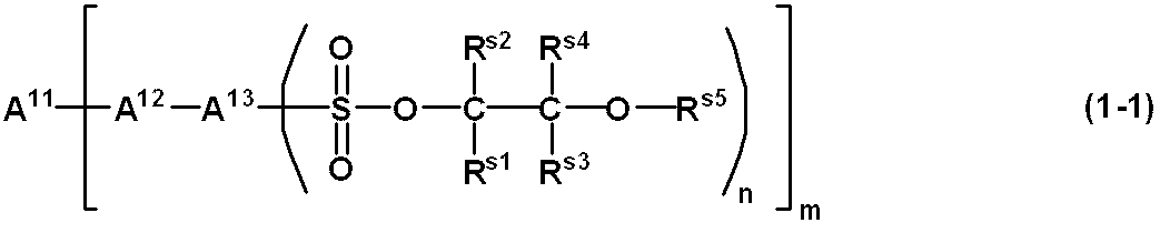
A11は、パーフルオロビフェニルから誘導されるm価の基であり、A12は、-O-又は-S-であり、A13は、ナフタレン又はアントラセンから誘導される(n+1)価の基であり;
m及びnは、前記と同じである。)

A14は、置換基を有していてもよい、1つ以上の芳香環を含むm価の炭化水素基であり、A15は、-O-又は-S-であり、A16は、(n+1)価の芳香族基であり;
m及びnは、前記と同じである。)
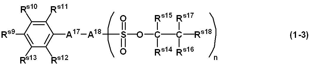
Rs14~Rs17は、それぞれ独立に、水素原子、又は直鎖状若しくは分岐状の炭素数1~20の1価脂肪族炭化水素基であり;
Rs18は、直鎖状若しくは分岐状の炭素数1~20の1価脂肪族炭化水素基、又は-ORs19であり、Rs19は、置換基を有していてもよい炭素数2~20の1価炭化水素基であり;
A17は、-O-、-S-又は-NH-であり;
A18は、(n+1)価の芳香族基であり;
nは、前記と同じである。) The charge transporting varnish according to any one of claims 1 to 4, wherein the arylsulfonic acid ester compound is represented by any one of the following formulas (1-1) to (1-3).
A 11 is an m-valent group derived from perfluorobiphenyl, A 12 is —O— or —S—, A 13 is a (n + 1) -valent group derived from naphthalene or anthracene Yes;
m and n are the same as above. )
A 14 is an m-valent hydrocarbon group containing one or more aromatic rings which may have a substituent, A 15 is —O— or —S—, and A 16 is n + 1) valent aromatic group;
m and n are the same as above. )
R s14 to R s17 are each independently a hydrogen atom or a linear or branched monovalent aliphatic hydrocarbon group having 1 to 20 carbon atoms;
R s18 is a linear or branched monovalent aliphatic hydrocarbon group having 1 to 20 carbon atoms, or -OR s19 , and R s19 has 2 to 20 carbon atoms which may have a substituent. A monovalent hydrocarbon group of
A 17 is -O-, -S- or -NH-;
A 18 is an (n + 1) -valent aromatic group;
n is the same as the above. ) - 前記3級アリールアミン化合物が、少なくとも2つの窒素原子を有し、かつ全ての窒素原子が3級アリールアミン構造を有するものである請求項1~5のいずれか1項記載の電荷輸送性ワニス。 The charge transporting varnish according to any one of claims 1 to 5, wherein the tertiary arylamine compound has at least two nitrogen atoms, and all the nitrogen atoms have a tertiary arylamine structure.
- 前記有機溶媒が、低極性有機溶媒である請求項1~6のいずれか1項記載の電荷輸送性ワニス。 The charge transporting varnish according to any one of claims 1 to 6, wherein the organic solvent is a low polarity organic solvent.
- 請求項1~7のいずれか1項記載の電荷輸送性ワニスから得られる電荷輸送性薄膜。 A charge transporting thin film obtained from the charge transporting varnish according to any one of claims 1 to 7.
- 請求項8記載の電荷輸送性薄膜を備える有機エレクトロルミネッセンス素子。 An organic electroluminescent device comprising the charge transporting thin film according to claim 8.
Priority Applications (5)
| Application Number | Priority Date | Filing Date | Title |
|---|---|---|---|
| US16/956,234 US20210078934A1 (en) | 2017-12-20 | 2018-12-19 | Charge-transporting varnish |
| JP2019560518A JP7310609B2 (en) | 2017-12-20 | 2018-12-19 | charge transport varnish |
| CN201880082195.5A CN111512459A (en) | 2017-12-20 | 2018-12-19 | Charge-transporting varnish |
| EP18890018.7A EP3731290A4 (en) | 2017-12-20 | 2018-12-19 | Charge-transporting varnish |
| KR1020207020935A KR20200098661A (en) | 2017-12-20 | 2018-12-19 | Charge transport varnish |
Applications Claiming Priority (2)
| Application Number | Priority Date | Filing Date | Title |
|---|---|---|---|
| JP2017-243550 | 2017-12-20 | ||
| JP2017243550 | 2017-12-20 |
Publications (1)
| Publication Number | Publication Date |
|---|---|
| WO2019124415A1 true WO2019124415A1 (en) | 2019-06-27 |
Family
ID=66994007
Family Applications (1)
| Application Number | Title | Priority Date | Filing Date |
|---|---|---|---|
| PCT/JP2018/046693 WO2019124415A1 (en) | 2017-12-20 | 2018-12-19 | Charge-transporting varnish |
Country Status (7)
| Country | Link |
|---|---|
| US (1) | US20210078934A1 (en) |
| EP (1) | EP3731290A4 (en) |
| JP (1) | JP7310609B2 (en) |
| KR (1) | KR20200098661A (en) |
| CN (1) | CN111512459A (en) |
| TW (1) | TWI808111B (en) |
| WO (1) | WO2019124415A1 (en) |
Cited By (2)
| Publication number | Priority date | Publication date | Assignee | Title |
|---|---|---|---|---|
| WO2020100013A1 (en) * | 2018-11-16 | 2020-05-22 | 株式会社半導体エネルギー研究所 | Organic compound, el device, light-emitting device, electronic equipment, lighting device and electronic device |
| WO2020218316A1 (en) * | 2019-04-26 | 2020-10-29 | 日産化学株式会社 | Method for producing arylsulfonic acid ester compound |
Families Citing this family (2)
| Publication number | Priority date | Publication date | Assignee | Title |
|---|---|---|---|---|
| KR102550692B1 (en) | 2018-04-24 | 2023-07-04 | 삼성디스플레이 주식회사 | Organic light emitting device and method manufacturing the same |
| CN114105838A (en) * | 2021-11-19 | 2022-03-01 | 北京大学深圳研究生院 | Flexible thermoelectric material and preparation method thereof |
Citations (28)
| Publication number | Priority date | Publication date | Assignee | Title |
|---|---|---|---|---|
| JPS5136795B2 (en) | 1971-11-12 | 1976-10-12 | ||
| JPS562191B2 (en) | 1976-03-13 | 1981-01-19 | ||
| WO1997049548A1 (en) * | 1996-06-25 | 1997-12-31 | Northwestern University | Organic light-emitting diodes and methods for assembly and emission control |
| WO2005094133A1 (en) | 2004-03-25 | 2005-10-06 | Hodogaya Chemical Co., Ltd. | Arylamine compound and organic electroluminescent device |
| WO2006025342A1 (en) | 2004-08-31 | 2006-03-09 | Nissan Chemical Industries, Ltd. | Arylsulfonic acid compound and use thereof as electron-acceptor material |
| JP2007137801A (en) * | 2005-11-16 | 2007-06-07 | Fuji Xerox Co Ltd | Charge transporting compound, charge transporting film and electroluminescent device using the same |
| WO2007099808A1 (en) * | 2006-02-23 | 2007-09-07 | Nissan Chemical Industries, Ltd. | Sulfonic acid ester compound and use thereof |
| WO2008032616A1 (en) | 2006-09-13 | 2008-03-20 | Nissan Chemical Industries, Ltd. | Oligoaniline compounds |
| WO2008129947A1 (en) | 2007-04-12 | 2008-10-30 | Nissan Chemical Industries, Ltd. | Oligoaniline compound |
| JP2009510795A (en) * | 2005-10-04 | 2009-03-12 | ゼネラル・エレクトリック・カンパニイ | Organic light-emitting device having latent activation layer and method of manufacturing |
| WO2010058777A1 (en) | 2008-11-19 | 2010-05-27 | 日産化学工業株式会社 | Charge transporting material and charge transporting varnish |
| JP2011022509A (en) * | 2009-07-17 | 2011-02-03 | Fujifilm Corp | Positive photosensitive resin composition for organic insulating film, organic insulating film, organic el display device and liquid crystal display device |
| WO2011132702A1 (en) | 2010-04-22 | 2011-10-27 | 日立化成工業株式会社 | Organic electronic material, polymerization initiator and thermal polymerization initiator, ink composition, organic thin film and production method for same, organic electronic element, organic electroluminescent element, lighting device, display element, and display device |
| WO2013098175A1 (en) | 2011-12-28 | 2013-07-04 | Solvay Sa | Crosslinkable arylamine compounds |
| JP5287455B2 (en) | 2008-04-16 | 2013-09-11 | 三菱化学株式会社 | Hole injection transport layer forming composition, method for manufacturing hole injection transport layer forming composition, organic electroluminescence device, organic EL display, and organic EL lighting |
| JP5381931B2 (en) | 2004-03-11 | 2014-01-08 | 三菱化学株式会社 | Charge transport film composition and ionic compound, charge transport film and organic electroluminescent device using the same, method for producing organic electroluminescent device, and method for producing charge transport film |
| WO2014073683A1 (en) | 2012-11-12 | 2014-05-15 | 三菱化学株式会社 | Organic electroluminescent element and method for manufacturing same |
| WO2014188998A1 (en) * | 2013-05-20 | 2014-11-27 | 日産化学工業株式会社 | Triphenylamine derivative and use therefor |
| WO2015050253A1 (en) | 2013-10-04 | 2015-04-09 | 日産化学工業株式会社 | Aniline derivatives and uses thereof |
| WO2015111654A1 (en) | 2014-01-27 | 2015-07-30 | 日産化学工業株式会社 | Aryl sulfonic acid compound and use of same |
| WO2015146965A1 (en) * | 2014-03-27 | 2015-10-01 | 日産化学工業株式会社 | Triarylamine derivative and use of same |
| WO2016006674A1 (en) | 2014-07-10 | 2016-01-14 | 日産化学工業株式会社 | Fluorine-atom-containing polymer and use thereof |
| JP5994213B2 (en) | 2011-05-31 | 2016-09-21 | 日立化成株式会社 | Electron-accepting compound and method for producing the same, polymerization initiator containing the compound, organic electronics material, organic thin film, organic electronics element, organic electroluminescent element, display element, lighting device, and display apparatus using the same |
| WO2016190326A1 (en) * | 2015-05-27 | 2016-12-01 | 日産化学工業株式会社 | Charge-transporting varnish, and organic electroluminescent element |
| JP6177771B2 (en) | 2011-06-17 | 2017-08-09 | メルク パテント ゲーエムベーハー | Materials for organic electroluminescent devices |
| CN107118206A (en) * | 2017-04-07 | 2017-09-01 | 同济大学 | The pyridine derivate Zn of one class quinoline two2+Fluorescence probe and its application |
| WO2017217457A1 (en) * | 2016-06-16 | 2017-12-21 | 日産化学工業株式会社 | Sulfonic acid ester compound and use therefor |
| WO2017217455A1 (en) * | 2016-06-16 | 2017-12-21 | 日産化学工業株式会社 | Sulfonic acid ester compound and use therefor |
Family Cites Families (4)
| Publication number | Priority date | Publication date | Assignee | Title |
|---|---|---|---|---|
| JP4596165B2 (en) * | 2003-06-25 | 2010-12-08 | 日産化学工業株式会社 | 1,4-Benzodioxane sulfonic acid compound and use as electron accepting substance |
| CN106030843B (en) * | 2014-02-18 | 2019-01-18 | 日产化学工业株式会社 | Charge-transporting varnish |
| JP6414213B2 (en) * | 2014-06-05 | 2018-10-31 | 日産化学株式会社 | Varnish for forming hole injection layer of organic electroluminescence device |
| EP3249710B1 (en) * | 2015-01-21 | 2019-11-13 | Nissan Chemical Corporation | Charge-transporting varnish, charge-transporting film, and organic electroluminescent element |
-
2018
- 2018-12-19 CN CN201880082195.5A patent/CN111512459A/en active Pending
- 2018-12-19 TW TW107145812A patent/TWI808111B/en active
- 2018-12-19 KR KR1020207020935A patent/KR20200098661A/en not_active Application Discontinuation
- 2018-12-19 EP EP18890018.7A patent/EP3731290A4/en not_active Withdrawn
- 2018-12-19 WO PCT/JP2018/046693 patent/WO2019124415A1/en unknown
- 2018-12-19 JP JP2019560518A patent/JP7310609B2/en active Active
- 2018-12-19 US US16/956,234 patent/US20210078934A1/en not_active Abandoned
Patent Citations (28)
| Publication number | Priority date | Publication date | Assignee | Title |
|---|---|---|---|---|
| JPS5136795B2 (en) | 1971-11-12 | 1976-10-12 | ||
| JPS562191B2 (en) | 1976-03-13 | 1981-01-19 | ||
| WO1997049548A1 (en) * | 1996-06-25 | 1997-12-31 | Northwestern University | Organic light-emitting diodes and methods for assembly and emission control |
| JP5381931B2 (en) | 2004-03-11 | 2014-01-08 | 三菱化学株式会社 | Charge transport film composition and ionic compound, charge transport film and organic electroluminescent device using the same, method for producing organic electroluminescent device, and method for producing charge transport film |
| WO2005094133A1 (en) | 2004-03-25 | 2005-10-06 | Hodogaya Chemical Co., Ltd. | Arylamine compound and organic electroluminescent device |
| WO2006025342A1 (en) | 2004-08-31 | 2006-03-09 | Nissan Chemical Industries, Ltd. | Arylsulfonic acid compound and use thereof as electron-acceptor material |
| JP2009510795A (en) * | 2005-10-04 | 2009-03-12 | ゼネラル・エレクトリック・カンパニイ | Organic light-emitting device having latent activation layer and method of manufacturing |
| JP2007137801A (en) * | 2005-11-16 | 2007-06-07 | Fuji Xerox Co Ltd | Charge transporting compound, charge transporting film and electroluminescent device using the same |
| WO2007099808A1 (en) * | 2006-02-23 | 2007-09-07 | Nissan Chemical Industries, Ltd. | Sulfonic acid ester compound and use thereof |
| WO2008032616A1 (en) | 2006-09-13 | 2008-03-20 | Nissan Chemical Industries, Ltd. | Oligoaniline compounds |
| WO2008129947A1 (en) | 2007-04-12 | 2008-10-30 | Nissan Chemical Industries, Ltd. | Oligoaniline compound |
| JP5287455B2 (en) | 2008-04-16 | 2013-09-11 | 三菱化学株式会社 | Hole injection transport layer forming composition, method for manufacturing hole injection transport layer forming composition, organic electroluminescence device, organic EL display, and organic EL lighting |
| WO2010058777A1 (en) | 2008-11-19 | 2010-05-27 | 日産化学工業株式会社 | Charge transporting material and charge transporting varnish |
| JP2011022509A (en) * | 2009-07-17 | 2011-02-03 | Fujifilm Corp | Positive photosensitive resin composition for organic insulating film, organic insulating film, organic el display device and liquid crystal display device |
| WO2011132702A1 (en) | 2010-04-22 | 2011-10-27 | 日立化成工業株式会社 | Organic electronic material, polymerization initiator and thermal polymerization initiator, ink composition, organic thin film and production method for same, organic electronic element, organic electroluminescent element, lighting device, display element, and display device |
| JP5994213B2 (en) | 2011-05-31 | 2016-09-21 | 日立化成株式会社 | Electron-accepting compound and method for producing the same, polymerization initiator containing the compound, organic electronics material, organic thin film, organic electronics element, organic electroluminescent element, display element, lighting device, and display apparatus using the same |
| JP6177771B2 (en) | 2011-06-17 | 2017-08-09 | メルク パテント ゲーエムベーハー | Materials for organic electroluminescent devices |
| WO2013098175A1 (en) | 2011-12-28 | 2013-07-04 | Solvay Sa | Crosslinkable arylamine compounds |
| WO2014073683A1 (en) | 2012-11-12 | 2014-05-15 | 三菱化学株式会社 | Organic electroluminescent element and method for manufacturing same |
| WO2014188998A1 (en) * | 2013-05-20 | 2014-11-27 | 日産化学工業株式会社 | Triphenylamine derivative and use therefor |
| WO2015050253A1 (en) | 2013-10-04 | 2015-04-09 | 日産化学工業株式会社 | Aniline derivatives and uses thereof |
| WO2015111654A1 (en) | 2014-01-27 | 2015-07-30 | 日産化学工業株式会社 | Aryl sulfonic acid compound and use of same |
| WO2015146965A1 (en) * | 2014-03-27 | 2015-10-01 | 日産化学工業株式会社 | Triarylamine derivative and use of same |
| WO2016006674A1 (en) | 2014-07-10 | 2016-01-14 | 日産化学工業株式会社 | Fluorine-atom-containing polymer and use thereof |
| WO2016190326A1 (en) * | 2015-05-27 | 2016-12-01 | 日産化学工業株式会社 | Charge-transporting varnish, and organic electroluminescent element |
| WO2017217457A1 (en) * | 2016-06-16 | 2017-12-21 | 日産化学工業株式会社 | Sulfonic acid ester compound and use therefor |
| WO2017217455A1 (en) * | 2016-06-16 | 2017-12-21 | 日産化学工業株式会社 | Sulfonic acid ester compound and use therefor |
| CN107118206A (en) * | 2017-04-07 | 2017-09-01 | 同济大学 | The pyridine derivate Zn of one class quinoline two2+Fluorescence probe and its application |
Non-Patent Citations (1)
| Title |
|---|
| JAPANESE JOURNAL OF APPLIED PHYSICS, vol. 45, no. 12, 2006, pages 9219 - 9223 |
Cited By (2)
| Publication number | Priority date | Publication date | Assignee | Title |
|---|---|---|---|---|
| WO2020100013A1 (en) * | 2018-11-16 | 2020-05-22 | 株式会社半導体エネルギー研究所 | Organic compound, el device, light-emitting device, electronic equipment, lighting device and electronic device |
| WO2020218316A1 (en) * | 2019-04-26 | 2020-10-29 | 日産化学株式会社 | Method for producing arylsulfonic acid ester compound |
Also Published As
| Publication number | Publication date |
|---|---|
| TWI808111B (en) | 2023-07-11 |
| EP3731290A4 (en) | 2021-09-29 |
| TW201939782A (en) | 2019-10-01 |
| US20210078934A1 (en) | 2021-03-18 |
| JPWO2019124415A1 (en) | 2020-12-24 |
| KR20200098661A (en) | 2020-08-20 |
| CN111512459A (en) | 2020-08-07 |
| JP7310609B2 (en) | 2023-07-19 |
| EP3731290A1 (en) | 2020-10-28 |
Similar Documents
| Publication | Publication Date | Title |
|---|---|---|
| JP6443588B2 (en) | Sulfonic acid ester compounds and use thereof | |
| JP6443587B2 (en) | Sulfonic acid ester compounds and use thereof | |
| JP7310609B2 (en) | charge transport varnish | |
| JP6760455B2 (en) | Aniline derivative and its manufacturing method | |
| JP7234937B2 (en) | Sulfonic acid ester compound and its use | |
| WO2015146965A1 (en) | Triarylamine derivative and use of same | |
| JP6424835B2 (en) | Aryl sulfonic acid compound and use thereof | |
| JP6551693B2 (en) | Charge transporting varnish, charge transporting thin film and method for producing the same, organic electroluminescent device and method for producing the same | |
| JP6402724B2 (en) | Arylsulfonic acid compounds and uses thereof | |
| JP6418234B2 (en) | Fluorene derivatives and uses thereof | |
| JP6488616B2 (en) | Charge transporting thin film forming varnish, charge transporting thin film and organic electroluminescent device | |
| WO2020262419A1 (en) | Charge-transporting varnish | |
| JPWO2019177043A1 (en) | Aniline derivatives and their uses | |
| JPWO2020009184A1 (en) | Composition for forming a charge-transporting thin film | |
| JP2015092561A (en) | Electric charge transportation type varnish, electric charge transportation type thin film and organic electroluminescent element | |
| JP6368943B2 (en) | Aryl sulfonic acid compound and use thereof, and method for producing aryl sulfonic acid compound | |
| JP6132016B2 (en) | Charge transport varnish |
Legal Events
| Date | Code | Title | Description |
|---|---|---|---|
| 121 | Ep: the epo has been informed by wipo that ep was designated in this application |
Ref document number: 18890018 Country of ref document: EP Kind code of ref document: A1 |
|
| ENP | Entry into the national phase |
Ref document number: 2019560518 Country of ref document: JP Kind code of ref document: A |
|
| NENP | Non-entry into the national phase |
Ref country code: DE |
|
| ENP | Entry into the national phase |
Ref document number: 20207020935 Country of ref document: KR Kind code of ref document: A |
|
| ENP | Entry into the national phase |
Ref document number: 2018890018 Country of ref document: EP Effective date: 20200720 |