WO2019124012A1 - 太陽電池 - Google Patents
太陽電池 Download PDFInfo
- Publication number
- WO2019124012A1 WO2019124012A1 PCT/JP2018/043782 JP2018043782W WO2019124012A1 WO 2019124012 A1 WO2019124012 A1 WO 2019124012A1 JP 2018043782 W JP2018043782 W JP 2018043782W WO 2019124012 A1 WO2019124012 A1 WO 2019124012A1
- Authority
- WO
- WIPO (PCT)
- Prior art keywords
- layer
- solar cell
- electrode
- absorption layer
- energy
- Prior art date
- Legal status (The legal status is an assumption and is not a legal conclusion. Google has not performed a legal analysis and makes no representation as to the accuracy of the status listed.)
- Ceased
Links
Images





Classifications
-
- H—ELECTRICITY
- H10—SEMICONDUCTOR DEVICES; ELECTRIC SOLID-STATE DEVICES NOT OTHERWISE PROVIDED FOR
- H10F—INORGANIC SEMICONDUCTOR DEVICES SENSITIVE TO INFRARED RADIATION, LIGHT, ELECTROMAGNETIC RADIATION OF SHORTER WAVELENGTH OR CORPUSCULAR RADIATION
- H10F77/00—Constructional details of devices covered by this subclass
- H10F77/20—Electrodes
-
- H—ELECTRICITY
- H10—SEMICONDUCTOR DEVICES; ELECTRIC SOLID-STATE DEVICES NOT OTHERWISE PROVIDED FOR
- H10F—INORGANIC SEMICONDUCTOR DEVICES SENSITIVE TO INFRARED RADIATION, LIGHT, ELECTROMAGNETIC RADIATION OF SHORTER WAVELENGTH OR CORPUSCULAR RADIATION
- H10F77/00—Constructional details of devices covered by this subclass
- H10F77/60—Arrangements for cooling, heating, ventilating or compensating for temperature fluctuations
- H10F77/63—Arrangements for cooling directly associated or integrated with photovoltaic cells, e.g. heat sinks directly associated with the photovoltaic cells or integrated Peltier elements for active cooling
- H10F77/67—Arrangements for cooling directly associated or integrated with photovoltaic cells, e.g. heat sinks directly associated with the photovoltaic cells or integrated Peltier elements for active cooling including means to utilise heat energy directly associated with the photovoltaic cells, e.g. integrated Seebeck elements
-
- Y—GENERAL TAGGING OF NEW TECHNOLOGICAL DEVELOPMENTS; GENERAL TAGGING OF CROSS-SECTIONAL TECHNOLOGIES SPANNING OVER SEVERAL SECTIONS OF THE IPC; TECHNICAL SUBJECTS COVERED BY FORMER USPC CROSS-REFERENCE ART COLLECTIONS [XRACs] AND DIGESTS
- Y02—TECHNOLOGIES OR APPLICATIONS FOR MITIGATION OR ADAPTATION AGAINST CLIMATE CHANGE
- Y02E—REDUCTION OF GREENHOUSE GAS [GHG] EMISSIONS, RELATED TO ENERGY GENERATION, TRANSMISSION OR DISTRIBUTION
- Y02E10/00—Energy generation through renewable energy sources
- Y02E10/50—Photovoltaic [PV] energy
- Y02E10/549—Organic PV cells
Definitions
- the present invention relates to a photovoltaic cell using photoelectric conversion and thermal energy.
- the solar cell is said to have a conversion efficiency of about 29.5% according to the Shockley-Quaser theory (see, for example, Non-Patent Document 1).
- a multijunction solar cell and a hot carrier solar cell have been proposed (see, for example, non-patent documents 2 to 4).
- a hot carrier solar cell is a principle that is generated by light absorption in a semiconductor layer, and the excited hot carrier is taken out to an electrode for a thermal relaxation time, for example, less than 1 ps (picosecond) in the case of silicon, Is difficult to realize, and no proof of principle has been made yet.
- An object of the present invention is to provide a solar cell capable of improving conversion efficiency.
- a solar cell using heat for power generation comprising: an absorption layer having a semiconductor material that generates first and second carriers upon receiving light; and the absorption layer.
- a first carrier provided between the first and second electrodes, the absorption layer, and the first electrode, the first carrier controlling movement from the absorption layer to the first electrode;
- a filter layer, and a second filter layer provided between the absorbing layer and the second electrode, the second carrier controlling the movement of the second carrier from the absorbing layer;
- the first and second filter layers are made of a semiconductor material, and the energy gap thereof is larger than the energy gap of the absorption layer, and the heat raises the temperature of the absorption layer to increase the temperature of the first and second electrodes. By raising the temperature It is possible to improve the conversion efficiency of the solar cell, the solar cell is provided.
- the energy gap of the first and second filter layers is larger than the energy gap of the absorption layer, when sunlight is received in the absorption layer, electron-hole pairs are generated, and the first filter layer Electrons having an energy greater than the energy gap of the first filter layer flow to the first electrode, and holes having an energy greater than the energy gap of the second filter layer pass through the second filter layer It passes and flows to the second electrode.
- the temperature of the absorbing layer is higher than the temperatures of the first and second electrodes, the heat energy of the absorbing layer, that is, the energy due to lattice vibration causes the energy of electrons and holes to be high, and the first and second electrodes are In each case, electrons and holes with high energy are taken out.
- the difference between the chemical potential of the first electrode and the chemical potential of the second electrode is increased, the open circuit voltage is increased, and a solar cell with improved conversion efficiency can be provided.
- electron-hole pairs generated in the absorption layer receiving light that is, carriers are high due to thermal energy obtained by converting a part of light energy of sunlight or thermal energy flowing into the absorption layer from the outside It takes advantage of being in an energy state.
- temperature of absorbing layer and “temperature of electrode” refer to temperatures measured by ordinary measurement, for example, a thermocouple thermometer, which are the principle of the present invention And in the explanation of simulation, in order to distinguish from the carrier temperature, they may also be expressed as “lattice temperature of absorption layer” and “lattice temperature of electrode”, respectively.
- FIG. 1 is a view showing the configuration of a solar cell according to an embodiment of the present invention.
- FIG. 2 is an energy diagram corresponding to the configuration of the solar cell according to the embodiment of the present invention.
- the solar cell 10 includes an absorbing layer 11, a first electrode 12 and a second electrode 13 provided on the absorbing layer 11, an absorbing layer 11, and A first filter layer 14 provided between the first electrode 12 and the second filter layer 15 provided between the absorption layer 11 and the second electrode 13 is provided.
- the first filter layer 14 and the second filter layer 15 are made of a semiconductor material, and a semiconductor material whose energy gap E g X is larger than the energy gap E g A of the semiconductor material of the absorption layer 11 is used.
- the absorption layer 11 In the solar cell 10, when the absorption layer 11 receives sunlight, one photon generates a pair of electron-hole pairs.
- the absorption layer 11 among the electrons having an energy distribution, electrons having an energy larger than the energy gap E g X of the first filter layer 14 pass through the first filter layer 14 and flow to the first electrode 12.
- holes having an energy larger than the energy gap of the second filter layer 15 pass through the second filter layer 15 and flow to the second electrode 13. In this manner, power is supplied to the load connected to the first electrode 12 and the second electrode 13 or the secondary battery (not shown).
- part of the light energy absorbed in the absorption layer 11 is converted to heat energy, or heat energy is supplied from the outside using a high-temperature body such as exhaust heat from a blast furnace or a plant or geothermal heat.
- a high-temperature body such as exhaust heat from a blast furnace or a plant or geothermal heat.
- the absorption layer 11 contains a semiconductor material, for example, silicon, amorphous silicon, SiC, BaSi 2 which is a silicide semiconductor, OsSi 2 , Ca 2 Si, etc., Se, a compound semiconductor such as InP, GaAs, AlSb, CdTe, CdSe.
- a semiconductor material for example, silicon, amorphous silicon, SiC, BaSi 2 which is a silicide semiconductor, OsSi 2 , Ca 2 Si, etc., Se, a compound semiconductor such as InP, GaAs, AlSb, CdTe, CdSe.
- materials having a perovskite crystal structure such as Al x Ga 1 -x As, Ga x In 1 -x As, In x Ga 1 -x P, In x Ga 1-x N, etc., which are multi-component mixed crystals MAPI (CH 3 NH 3 PbI 3 ), an analog in which this lead (Pb) is replaced with Sn or Ge, formamidinium lead iodide (FAPI), complex halide (FA, MA) PbI 3 (FAMAPI), and the like Analogs, CIGS materials (compounds using Cu, In, Ge, Se, S as raw materials), CZTS materials (compounds using Cu. Zn, Sn, S as raw materials), organic semiconductors Ofen (P3HT) etc. are mentioned.
- the absorbing layer 11 is preferably smaller than the thermal conductivity of the first electrode 12 and the second electrode 13. As a result, the conduction of heat from sunlight or the like to the first electrode 12 and the second electrode 13 is suppressed, heat is stored in the absorption layer 11, and the temperature rises.
- the absorption layer 11 preferably has a thickness equal to or less than the minority carrier diffusion length. Thereby, heat is stored and the temperature rises. Moreover, it is preferable that the absorption layer 11 texturing is performed to the surface 11a which sunlight injects, the surface 11b on the opposite side, or both. In this way, for ideal texturing, all absorption conditions in the Yablonovitch limit (E. Yablonovitch, “Statistical ray optics”, J. Opt. Soc. Am., 1982, Vol. 72, p. 899) are realized, The thickness w A can satisfy the relation w A > 1 / (4 n 2 ⁇ ).
- ⁇ is the absorption coefficient (cm ⁇ 1 ) of the absorption layer 11.
- a semiconductor having an oxide semiconductor for example, amorphous silicon (1.4 to 1.8 eV, including mixed crystals with SiC etc.), silicide semiconductor BaSi 2 (1.3 eV), OsSi 2 (1.8 eV , Ca 2 Si (1.9 eV), etc., Se (1.74 eV), and as a compound semiconductor, InP (1.35 eV), GaAs (1.42 eV), AlSb (1.6 eV), CdTe (1.
- oxide semiconductor for example, amorphous silicon (1.4 to 1.8 eV, including mixed crystals with SiC etc.), silicide semiconductor BaSi 2 (1.3 eV), OsSi 2 (1.8 eV , Ca 2 Si (1.9 eV), etc., Se (1.74 eV), and as a compound semiconductor, InP (1.35 eV), GaAs (1.42 eV), AlSb (1.6 eV), CdTe (1.
- CdSe (1.73 eV) such as Al x Ga 1 -x As (1.42 to 2.16 eV) which is a multicomponent compound mixed crystal, Ga x In 1-x As (0.36 to 1.42 eV) ), In x Ga 1-x P (1.35-2.26 eV), In x Ga 1-x N (0.7-3.4 eV) ))
- MAPI CH 3 NH 3 PbI 3
- FAPI formamidinium lead iodide
- FAMAPI complex halide
- CIGS materials compounds using Cu, In, Ge, Se, S as raw materials
- CZTS materials Cu.
- () indicates the range of possible energy gaps of the respective semiconductor materials, and when applied to the solar cell 10, a semiconductor having an energy gap E g X larger than the energy gap E g A of the absorbing layer 11 It is selected from the materials and their compositions.
- the first filter layer 14 and the second filter layer 15 may use semiconductor materials having different energy gaps. However, for convenience of description, the first filter layer 14 and the second filter layer 15 are described as semiconductor materials having the same energy gap.
- the first electrode 12 and the second electrode 13 are made of a conductive material, for example, metals such as aluminum, nickel, copper, palladium, silver, platinum, gold and the like, and alloys thereof, semiconductor materials such as silicon doped with impurity ions Titanium oxide (TiO 2 ), tin-doped indium oxide (ITO), zinc oxide (ZnO), aluminum oxide (Al 2 O 3 ), AZO (ZnO: Al), GZO (ZnO: Ga), ATO (SnO 2 : It is selected from conductive metal oxides such as Sb), FTO (SnO 2 : F), ZnMgO, and mixtures thereof, conductive pastes, and the like.
- the first electrode 12 and the second electrode 13 may each be formed by laminating the above-described different conductive materials.
- the absorbing layer 11 has an n-type doped region 11 n in a portion in contact with the first filter layer 14 and a p-type doped region 11 p in a portion in contact with the second filter layer 15.
- the absorption layer 11 is Si
- the dopant for example, P, As, Sb can be used as the n-type doped region 11 n
- B, Al, Ga, In can be used as the p-type doped region 11 p.
- an n-type doped region may be provided in the first filter layer 14 and a p-type doped region may be provided in the second filter layer 15.
- the electrode 12 may be provided with an n-type doped region, the second electrode may be provided with a p-type doped region, or these may be appropriately combined.
- an insulating layer may be provided at least between the two electrodes 13.
- the time for taking out the carrier from the absorbing layer 11 to the first electrode 12 and / or the second electrode 13 can be adjusted, and the heat flow can be indirectly controlled.
- an electrically insulating material or a semiconductor material not doped with a dopant can be used.
- the carrier extraction time is the time from the generation of carriers (electron-hole pairs) to the extraction to the first electrode 12 or the second electrode 13.
- the absorption layer 11 may form a passivation layer (not shown) in the part which the surface exposes.
- a passivation layer for example, amorphous silicon (a-Si: H), thermal oxide film (SiO 2 ), silicon nitride film (a-Si 1-x N x : H) can be used.
- the first electrode 12 and the second electrode 13 are disposed on the surface 11b opposite to the surface 11a of the absorption layer 11 on which the sunlight is incident, shadow loss of sunlight can be avoided. Further, since the first electrode 12 and the second electrode 13 are disposed on one surface 11 b on the absorbing layer 11, the first electrode 12, the first filter layer 14, the second electrode 13 and the second filter layer 15 are It is easy to form.
- the first electrode 12 and the second electrode 13 will be described below as metal materials for the convenience of description, but when the solar cell 10 receives the light from the absorption layer 11, one photon is separated from the other. Electron-hole pairs are generated. That is, when the energy of the received light is larger than the energy gap E g A of the absorption layer 11, electrons are excited from the valence band VLB to the conduction band CDB. Electron conduction band CDB absorbent layer 11, absorption layer 11 when the temperature than the first electrode 12 is high, with the thermal energy E A from the lattice of the absorbing layer 11, its energy increases.
- the energy gap E g X of the first filter layer 14 is larger than the energy gap E g A of the absorbing layer 11, the electrons that can flow out to the first electrode 12 have their increased energy be the energy gap E of the first filter layer 14 It is larger than g X.
- a hole in the valence band VLB of the absorber layer 11, with the thermal energy E A from the lattice of the absorbing layer 11, its energy increases.
- the energy gap E g X of the second filter layer 15 is larger than the energy gap E g A of the absorbing layer 11, the increased energy of holes that can flow out to the second electrode 13 is the energy gap of the second filter layer 15 It is larger than E g X. This mechanism is explained in more detail in FIG.
- FIG. 3 is a view for explaining the operation of the solar cell according to one embodiment of the present invention, and for the convenience of description, the side from which electrons flow as carriers, that is, the absorption layer 11 and the first filter layer 14 (Hereinafter, it is abbreviated as “filter layer 14") and the first electrode 12 (hereinafter, abbreviated as “electrode 12") will be described in detail.
- (a) is an example of the solar cell 10 which concerns on this embodiment, is an example in which the filter layer 14 is provided,
- (b) is an example in which the filter layer is not provided as a comparative example.
- the left side of each of (a) and (b) shows the carrier distribution N c A flowing out from the absorption layer 11 to the electrode 12, and the right side shows the carrier distribution N c E flowing from the electrode 12 into the absorption layer 11. .
- the hatched portion corresponds to the carrier distribution flowing in and out.
- the horizontal axis of each figure is the carrier density N c
- the vertical axis is the energy E.
- the absorption layer 11 when the temperature T PH of the absorption layer 11 shown in the upper part is equal to the temperature T c of the electrode 12 of the solar cell 10, the absorption layer 11 is The carrier distribution N c A flowing out from the electrode 12 to the carrier distribution N c E flowing from the electrode 12 into the absorbing layer 11 is equal, whereby the carrier distribution having an energy larger than the energy gap E g X of the filter layer 14 (Hatched parts) are equal to one another.
- the carrier energy of the absorption layer 11 increases due to the increase of the temperature T PH of the absorption layer 11 Carrier distribution N c A spreads to the high energy side. Accordingly, carriers having energy larger than the energy gap E g X of the filter layer 14 flow out from the absorbing layer 11 to the electrode 12. As a result, the chemical potential (chemical potential ⁇ c shown in FIG. 2) of the electrode 12 is increased, the open circuit voltage of the solar cell 10 is increased, and the conversion efficiency of the solar cell 10 is improved. Further, it is understood that the higher the temperature T PH of the absorbing layer 11 is, the more preferable it is in that the open circuit voltage of the solar cell 10 is increased.
- the carrier distribution N c A and the carrier distribution It is equal to N c E.
- the carrier energy of the absorption layer 11 is increased by the temperature increase of the absorption layer 11, and the carrier distribution N c A is high energy Spread to the side.
- the same hole outflow occurs on the side from which the holes flow out, that is, the side from which the electrons flow out of the absorption layer 11, the second filter layer 15, and the second electrode 13 as well. That is, the chemical potential (chemical potential ⁇ v shown in FIG. 2) changes in the direction in which the absolute value of ⁇ c - ⁇ v increases, and the open circuit voltage of the solar cell 10 increases. As a result, conversion of the solar cell 10 Efficiency is improved.
- FIG. 4 is a schematic perspective view of a solar cell according to an embodiment of the present invention.
- the solar cells 20 extend in the Y direction and are alternately arranged in the X direction on the absorption layer 11 and the surface 11 b opposite to the surface 11 a on which the sunlight is incident.
- a first electrode 121,2 and a first filter layer 141,2 and a second electrode 131,2 and a second filter layer 151,2 are provided.
- the n-type doped region and the p-type doped region are not shown.
- the first electrode 12 1 and the first filter layer 14 1 and the second electrode 13 1 and the second filter layer 15 1 has the X-direction interval L 1, L 2.
- the spacings L 1 and L 2 are preferably arranged to be larger than the widths D 1 and D 2 . As a result, the heat flow from the absorbing layer 11 to the first electrode 121, 2 and the second electrode 131, 2 can be suppressed, and the temperature of the absorbing layer 11 can be further raised.
- the width D 1 may be the same as the width D 2, may be different.
- Distance L 1 may be the same as the spacing L 2, it may be different.
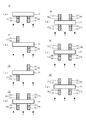
- FIG. 5 is a view showing the configuration of a modification of the solar cell according to one embodiment of the present invention.
- the arrangement of the first electrode 12 and the first filter layer 14 is different from the arrangement of the second electrode 13 and the second filter layer 15. It is a modification of the solar cell 10 shown to.
- a laminate of the first electrode 12 and the first filter layer 14 is referred to as a first laminate 16, and a laminate of the second electrode 13 and the second filter layer 14 is referred to as a second laminate 17.
- the arrow on the lower side of each figure represents the incident direction of sunlight.
- the solar cell 30 is provided with the first stacked body 16 and the second stacked body 17 on the surface of the absorption layer 11 on which the sunlight is incident. Thereby, the solar cell 30 can be easily provided in contact with the absorption layer 11 with an infrared absorption layer described later on the surface opposite to the surface on which the sunlight is incident.
- the solar cell 31 is provided with the first stacked body 16 on the surface of the absorption layer 11 on which the sunlight is incident, and the second stacked body 17 is the absorption layer 11.
- the surface of the absorption layer 11 which provides the 1st laminated body 16 and the 2nd laminated body 17 is reverse. Note that one of these solar cells 31 and solar cells 32 may be combined with each other to form a solar cell having a plurality of cells.
- the solar cell 33 is provided with one of the first laminate 16 1 and the other of the first stacked body 16 2 is spaced to the surface of the sunlight-incident side of the absorbent layer 11 is, 2 one of the second laminate 17 1 and the other for the second stack 17 is provided on the opposite side of the absorbent layer 11. Furthermore, the solar cell 33, first laminate 16 1 and has a 1 second stack 17 is arranged on opposite sides of the absorbent layer 11, and the 2 first laminate 16 and second laminate 17 2 Are disposed to face each other across the absorption layer 11.
- the solar cell 34 has one surface on the side opposite to the incident side surface of the sunlight first laminate 16 1 and the other of the first laminate 16 2 absorption layer 11 the provided spaced apart, 2 one of the second laminate 17 1 and the other for the second stack 17 is provided on a surface of the sunlight-incident side of the absorbent layer 11.
- the first and the laminate 16 1 has a 1 second stack 17 is arranged on opposite sides of the absorbing layer 11, a first laminate 16 2 and 2 second stack 17 across the absorbing layer 11 It is arranged facing each other.
- the solar cell 35 one first laminate 16 1 is provided on the surface of the incident side of sunlight absorption layer 11, the first laminate 16 2 of the other absorbent It is provided on the opposite side of the layer 11 and is disposed opposite to each other with the absorbing layer 11 in between.
- Solar cell 35 has one second laminate 17 1 is provided on a surface of the incident side of sunlight absorption layer 11, the second stack 17 2 the other is provided on the opposite side of the absorbent layer 11 is, the second laminate 17 1 and a 2 second stack 17 are arranged on opposite sides of the absorbent layer 11.
- First laminate 16 1 and 1 second stack 17 are spaced apart from the surface on the side where the incident sunlight, and the first laminate 16 2 and 2 second laminate 17 is on the opposite side It is placed apart.
- the solar cell 36 one first laminate 16 1 is provided on the surface of the incident side of sunlight absorption layer 11, the first laminate 16 2 of the other absorbent It is provided on the opposite side of the layer 11.
- Solar cell 36 has one second laminate 17 1 is provided on a surface of the incident side of sunlight absorption layer 11, the second stack 17 2 the other is provided on the opposite side of the absorbent layer 11 It is done.
- First laminate 16 1 and has a 2 second stack 17 is arranged on opposite sides of the absorbing layer 11, a first laminate 16 2 and 1 second stack 17 across the absorbing layer 11 It is arranged facing each other.
- the first stacked body 161 , 2 and the second stacked body 171, 2 the first stacked body 161 , 2 and / or It is preferable not to arrange the laminates 171 and 2 in that shadow loss can be avoided.
- the arrangement of the solar cells 35 is preferable, and the arrangement of the solar cells 33, 34, 36 is more preferable, in that the recovery rate of the carriers generated in the absorption layer 11 is high.
- the absorption layer 11 is first laminated body 16 1, 2 or point tends to form a second stack 17 1,2 on, the solar cell 34 and 35 is preferred, the solar cell 30, 31, 32 is more preferred.
- the n-type doped region 11n and the p-type doped region 11p shown in FIG. 1 are omitted in FIGS. 5 (a) to 5 (g), they are provided in the same manner.
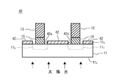
- FIG. 6 is a view showing the configuration of another modification of the solar cell according to one embodiment of the present invention.
- the solar cell 40 has an infrared absorbing layer 42 in contact with the surface 11b opposite to the surface 11a of the absorbing layer 11 irradiated with sunlight, and the other configuration is shown in FIG. It is similar to the solar cell 10.
- the infrared absorbing layer 42 is made of a material having a high absorptivity in the infrared wavelength region, and examples thereof include a member to which nitric acid treatment NiP plating has been applied, VANTA black, Metal Velvet (registered trademark), and the like.
- the infrared absorption layer 42 By absorbing light transmitted through the absorption layer 11, particularly infrared rays, and converting it into heat, the temperature of the infrared absorption layer 42 rises, and the absorption layer 11 in contact therewith is heated by heat conduction to raise the temperature of the absorption layer 11 can do. That is, the infrared absorption layer 42 functions as a heating unit of the absorption layer 11.
- the infrared absorbing layer 42 is provided with an air gap in order to prevent the side surface 42 a of the first electrode 12 and the first filter layer 14 from contacting each other.
- the infrared absorbing layer 42 is provided with an air gap in order to prevent the side surface 42 b of the infrared absorbing layer 42 from contacting the second electrode 13 and the second filter layer 15. Thereby, the heat flow is prevented from flowing from the infrared absorption layer 42 to the first electrode 12 and the second electrode 13, and the temperature rise of the first electrode 12 and the second electrode 13 is suppressed.
- the infrared absorption layer 42 is conductive, it is preferable to provide an insulating layer (not shown) that electrically insulates between the infrared absorption layer 42 and the absorption layer 11.
- the infrared absorbing layer 42 may be replaced with a heat conductor (not shown) having a good heat conductivity, and the heat conductor may be supplied with heat energy from the outside.
- the absorption layer 11 can be heated.
- a heat energy source exhaust heat of a plant, geothermal heat, etc. can be used, and what condensed sunlight and converted into thermal energy may be supplied. Heat may be supplied to the absorption layer 11 from the outside without providing a heat conductor.
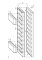
- FIG. 7 is an exploded perspective view showing the configuration of another modification of the solar cell according to one embodiment of the present invention.
- the solar cell 50 includes an absorption layer 51 stacked so that the first semiconductor layer 51 a and the second semiconductor layer 51 b are electrically conductive, and the second semiconductor layer 51 b . , And a laminate of the first filter layer 14 and the first electrode 12 and a laminate of the second filter layer 15 and the second electrode 13 which are separated from each other.
- the first semiconductor layer 51 a and the second semiconductor layer 51 b respectively to form a row in which a plurality of holes 51 ah, 51 bh are periodically arranged in the Y direction through the thickness direction (Z direction),
- the columns are periodically arranged in the X direction.
- the phonon transport that propagates heat in the in-plane direction of the absorption layer 51 that is, the X direction and the Y direction is inhibited, so that the thermal conductivity can be reduced.
- Heat conduction to the laminate of the electrode 12 and the laminate of the second filter layer 15 and the second electrode 13 can be suppressed, and heat can be stored in the absorption layer 51 to raise its temperature.
- a first semiconductor layer 51 a and the second semiconductor layer 51 b, the hole portion 51 ah, 51 bh are stacked so as not to overlap each other. Thereby, the reduction of the light absorption area can be suppressed.
- the hole 51 bh may or may not be provided on the lower surface of the first filter layer 14 and the second filter layer 15 as shown in FIG. 7.
- the holes 51 ah and 51 bh preferably have an inner diameter of 1 ⁇ m or less in that the thermal conductivity in the in-plane direction (XY direction) due to the phononic crystal structure is sufficiently reduced.
- the holes 51 ah and 51 bh are cylindrical hollows in FIG. 7, the present invention is not limited thereto, and may be polygonal hollows.
- the holes 51 ah and 51 bh preferably have a gap of 1 ⁇ m or less from the viewpoint of sufficiently reducing the thermal conductivity in the in-plane direction (X-Y direction) by the phononic crystal structure.
- first filter layer 14 and the first electrode 12 and the second filter layer 15 and the second electrode 13 in the X direction is sufficiently larger than the width (thickness) in the X direction, they will be described with reference to FIG.
- the intervals are shown as narrow for convenience.
- the solar cell 50, the in-plane direction of the thermal conductivity of the absorber layer 51, and the first semiconductor layer 51 a and the second semiconductor layer 51 b is a two-dimensional phononic crystal structure thermal Since the conduction is suppressed, the heat absorption of the absorption layer 51 is facilitated, and the temperature can be maintained high. Thereby, the solar cell 50 with high conversion efficiency can be realized.
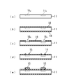
- FIG. 8 is a manufacturing process diagram of a solar cell according to an embodiment of the present invention. Each step will be described below with reference to FIGS. 8 (a) to 8 (e).
- the absorption layer 11 is formed, and then the absorption layer 11 is doped with N-type and P-type dopants.
- silicon Si
- Si is formed to a thickness of 10 ⁇ m by, for example, a chemical vapor deposition (CVD) method as the absorption layer 11.
- CVD chemical vapor deposition
- a first filter layer / first electrode and a second filter layer / second layer formed downstream of the manufacturing process by combining patterning method, for example, photolithography, chemical etching, laser processing, etc.
- a mask having an opening at the position of two electrodes is formed.
- an n-type doped region 11n and a p-type doped region 11p are formed by using, for example, an ion implantation method, a thermal diffusion method, a CVD method, and the like, using an N-type dopant and a P-type dopant, respectively.
- the passivation layer 18 is formed on the surface of the absorption layer 11. Specifically, the passivation layer 18 forms a thin film of, eg, a 10 nm-thick amorphous silicon (a-Si: H) by a CVD method.
- a-Si: H amorphous silicon
- a part of the passivation layer 18 is etched to expose the surface of the absorption layer 11. Specifically, the etching is performed, for example, by forming a resist and performing patterning, and a part of the passivation layer 18 is removed by chemical etching, dry etching or the like to form an opening 18 a.
- the first and second filter layers 14 and 15 are formed on the surface of the absorbing layer 11 exposed by the opening 18a.
- the first and second filter layers 14 and 15 each have, for example, a 10 nm-thick a-Si: H film formed by the CVD method.
- the first and second electrodes 12 and 13 are stacked on the first and second filter layers 14 and 15, respectively.
- silver is used to form, for example, a thickness of 30 ⁇ m by a printing method, an evaporation method, a sputtering method, or the like.
- the solar cell according to the present embodiment is formed.
- the first and second filter layers 14 and 15 and the first and second electrodes 12 and 13 may be arranged as in the modification of FIG. 5 described above. Further, the infrared absorption layer 42 shown in FIG. 6 may be formed on the surface of the absorption layer 11 by removing the passivation layer 18 or may be formed on the passivation layer 18.
- silicon is used for the absorption layer, and the solar cell conversion efficiency for the operating voltage and the energy gap of the filter layer, the temperature of the absorption layer and the solar cell for the energy gap of the filter layer
- the open circuit voltage with respect to the temperature of the absorption layer and the energy gap of the filter layer was determined by simulation.
- Rate equation for microscopic distribution function of carriers in absorption layer and solution under steady conditions The energy bands of the electrons in the conduction band and the holes in the valence band of the absorption layer are described using a two-band effective mass approximation consisting of two bands.
- energy based on the bottom of each band is E e (> 0) and E h (> 0) for electrons and holes, respectively.
- Distribution functions of electrons having energy E e and holes having E h (number of occupation of carriers occupying one energy eigenstate) n e Ee , n h Eh are rate equations of the following formulas 1 and 2 It is determined.
- the right side of the first equal sign of Formula 1 and Formula 2 is the generation or loss rate of carriers in each energy state.
- J e, sun Ee and J h, sun Eh is an electronic, generation rate of the hole of the absorbent layer by the respective solar absorber.
- J e, rad Ee and J h, rad Eh are each electron absorption layer by radiative recombination, holes loss rate.
- J e, out Ee and J h, out Eh are the loss rates of electrons and holes in the absorption layer due to extraction to the electrode, respectively.
- Equation 1 and Equation 2 By setting the right side of the second equal sign of Equation 1 and Equation 2 to zero, stationary conditions under constant sunlight irradiation conditions are imposed.
- Each generation or loss rate is derived by the microscopic model as an indirect semiconductor and the absorption layer is given as follows.
- the electron and hole generation rates are represented by Formula 3 and Formula 4 below, respectively.
- ⁇ (E) is the light absorption coefficient of the absorption layer at energy E
- the energy gap of the absorption layer is E g A
- the effective masses of electrons and holes are m e * and m h * , respectively.
- the incident sunlight spectrum (The photon number energy density at energy E incident per unit time per unit area is approximated as follows by the black body radiation spectrum under the condition of zero air mass) did.
- CR is a focusing magnification
- c is the speed of light in vacuum
- R S is the radius of the sun
- L ES is the average distance between the sun and the earth
- D 0 ⁇ (E) E 2 / ( ⁇ 2 h 3 c 3 )
- h Planck's constant / (2 ⁇ )
- T s is the surface temperature of the sun
- k B is Boltzmann's constant.
- the electron-hole recombination loss rate (second term on the right side of the first equal sign of Formula 1 and Formula 2) is represented by the following Formula 6 and Formula 7, respectively.
- the extraction rates of electrons and holes to the electrode are represented by the following Formula 8 and Formula 9, respectively.
- ⁇ out is a carrier extraction time
- E g X is an energy gap of the filter layer.
- ⁇ (z) is a step function which becomes 1 at z> 0.
- the distribution functions at the electron-side and hole-side electrodes are given by the Fermi distribution function of the following equation 10, where the environmental temperature T c and the Fermi energy ⁇ are ⁇ c and ⁇ v respectively.
- the difference between the Fermi energy at the electron side and the hole side electrode and the operating voltage V of the solar cell is expressed by the following equation 11.
- q is an elementary charge.
- the intra-band thermal relaxation rate of electrons and holes (fourth term on the right side of the first equivalent of the formulas 1 and 2) is represented by the following formula 12.
- W e (h) Ei, Ef in electron (hole) band scattering from the initial state with energy E i to the final state with E f, or phonon scattering intensity of the carrier about the reverse process It is a parameter.
- This specific expression is determined by designating the type of phonon involved with the absorption layer. In the numerical calculation for the absorption layer silicon, LA phonon was incorporated as a factor of phonon relaxation.
- f B Tph is the distribution function (Bose-Einstein distribution) of phonons at the lattice temperature T ph and is given by the following equation 13.
- Equation 1 and Equation 2 are obtained with respect to the distribution functions ne e Ee and n h Eh of carriers having all the energy in the band of the absorption layer.
- the energy conversion efficiency ⁇ of the solar cell can be obtained by the following equation 17 using these.
- the energy flow related to the solar cell 10 of the present embodiment includes four energy flows in addition to the above-described solar light incident energy flow P SUN and the work P WORK extracted as electric power.
- PT is a transmission energy flow which is a transmission loss without being absorbed by the absorption layer 11
- P Rad is an energy flow of radiation recombination loss due to light emission recombination in the absorption layer 11
- P Qout is a heat discharged to the electrodes 12 and 13
- the energy flow, P Qin is the energy flow discharged to the lattice of the absorbing layer 11.
- the transmitted energy flow P T is given by Equation 18 below.
- Equation 19 The radiation recombination loss P Rad per unit area is given by the following Equation 19.
- the thermal energy flow P Qout discharged to the electrode is given by Equation 20 below. Also in this case, the distribution function in the absorption layer can be evaluated using the stationary solution of the microscopic rate equation.
- Equations 22 and 23 can be obtained as follows.
- the terms that contribute to the change per unit time of the total number of charges in Equations 1 and 2 are Equations 8 and 9, respectively.
- the number of electron outflows from the absorption layer to the electrode (electron side) per unit time is from the left side of the second equation of Eq. 14, and the number of holes outflow from the absorption layer to the electrode (hole side) per unit time is As long as the second equation of equation (14) is given by the right side of the second equation of the equation, the situation is realized that the total number of electrons and holes flowing out from the absorber layer is equal and there is no temporal variation of the total charge in the absorber layer. Do.
- Equation 24 balances the left side, which means the total number of charges flowing out from the absorption layer to the electrode per unit time, and the right side, which means the total number of charges coming from the electrode to the absorption layer per unit time, It simply means that the net total number of charges in the absorption layer does not fluctuate with time.
- the right side of Equation 24 is 0 (zero) as the condition for the total number of charges per unit time from the electrode to the absorption layer to be zero in Equation 24, the following Equation 25 is obtained.
- Equation 27 Since the content of the first bracket is positive and can not be zero in the left side of Equation 27, the condition that Equation 27 holds is that the content of the second bracket is zero, so the following equation 28 are obtained.
- Formula 22 and Formula 23 are obtained from Formula 29 and Formula 11. That is, under charge neutral conditions in the absorbing layer, the chemical potential at each electrode as a function of the potential difference V is given by Equations 22 and 23.
- Equation 3 Equation 4
- Equation 6 Equation 7, Equation 8, Equation 9, Equation 9 for each generation or loss rate
- Equation 12 the distribution functions ne e Ee and n h Eh regarding all the energies E e and E h which are unknown variables in the rate equation (Eq. 1 and Eq. 2 second equations) remain.
- Equation 9 Equation 9 for each generation or loss rate
- Equation 1 and Equation 2 are written down for all the energy E e and E h , a closed multivariable nonlinear simultaneous equation to be solved for the distribution functions n e Ee and n h Eh is determined Do.
- the distribution functions ne e Ee and n h Eh for all the energy E e and E h can be obtained as a function of the voltage V and other setting parameters.
- equation 8 is substituted into equation 15
- equation 5 is substituted into equation 16
- the value of distribution function determined as a solution of rate equation is substituted into them.
- the conversion efficiency ⁇ was determined for various operating voltages V by substituting P WORK and P SUN obtained thereby into Equation 17. Furthermore, the maximum conversion efficiency and open circuit voltage for each condition were determined while changing the energy gap of the filter layer, the carrier extraction time, the absorption layer temperature, the light collection ratio and the like.
- FIG. 9 is a diagram in which the conversion efficiency of the solar cell according to an embodiment of the present invention is obtained by simulation with the energy gap of each filter layer with respect to the extraction voltage.
- FIG. 10 is a diagram showing the maximum conversion efficiency of the solar cell according to an embodiment of the present invention obtained by simulation at each temperature with respect to the energy gap of the filter layer.
- FIG. 10 plots the same simulation as FIG. 9 with the temperature of the absorption layer changed, with the abscissa representing the energy gap E g X of the filter layer and the ordinate representing the maximum value ⁇ max of the conversion efficiency.
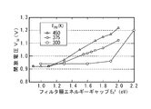
- FIG. 11 is a diagram showing the open circuit voltage of the solar cell according to an embodiment of the present invention obtained by simulation at each temperature with respect to the energy gap of the filter layer.
- FIG. 11 is a simulation similar to FIG. 9 but with the temperature of the absorption layer changed, and the horizontal axis is plotted as the energy gap E g X of the filter layer, and the vertical axis is shown as the open circuit voltage V OC .
- the open circuit voltage V OC is constant at 0.92 eV below 1.12 eV of the energy gap E g A of silicon, but at E G A In the energy gap E g X larger than 1.12 eV, it can be seen that the open circuit voltage V OC increases as the E g X increases. Also, when T PH is compared between 375 K and 450 K, the open circuit voltage V OC is higher at 450 K. This means that the carrier energy of the absorption layer 11 is increased, the carrier distribution N c A is shifted to the high energy side, and the energy larger than the energy gap E g X of the filter layer 14 as described in FIG. The carrier is generated by flowing out of the absorbing layer 11 to the electrode 12. The same is true for holes.
- the heat flow P Qin flowing from the incident sunlight into the absorber lattice is calculated in equation 21 above, and the absorber lattice can be warmed if P Qin is positive.
- L, D, w A respectively indicate the first filter layer 141, 2 and the second filter layer 151, 2 (shown in FIG.
- the average temperature rise of the absorption layer was determined with respect to the distance between the electrodes when the conditions for the solar cell of the present embodiment to operate stably were satisfied. Taking out time ⁇ out , absorbing layer temperature T PH , electrode temperature T c , condensing ratio CR, and filter layer energy gap E g X as shown in Table 1 below, the absorbing layer is calculated from the above equation 21 The heat flow P Qin discharged to the grid was calculated. The distance L is selected from the equation 30 so that the temperature rise due to the heat flow P Qin matches the difference between T PH and T c shown in Table 1. The energy flow and the interval L are shown in Table 1.
- the interval L is sufficiently larger than the width D (L >> D), and the Jablonovich limit described above is adopted on the assumption that ideal texturing is performed for light absorption.
- the thickness w A was 10 ⁇ m, and the thermal conductivity ⁇ of the absorption layer 11 in the in-plane direction was 1 W / (m ⁇ K).
- FIG. 12 is a view showing the relationship between the average temperature rise of the absorption layer and the distance between the electrodes that satisfy the conditions for the solar cell of the example to operate stably. Referring to FIG. 12, the conditions for stably operating the solar cell of the present example satisfying the above equation 30 are shown for the three conditions in Table 1.
- the infrared absorption layer 42 absorbs the transmitted energy flow PT which causes transmission loss without the incident sunlight being absorbed by the absorption layer 11, and the heat thereof
- the average temperature increase is estimated by the following equation 31.
- the average temperature rise of the absorption layer 11 can be increased.
- the carrier energy of the absorption layer 11 is increased by the rise of the temperature T PH of the absorption layer 11, and the carrier distribution N c A is shifted to the high energy side.
- the open circuit voltage of the battery is increased, and the conversion efficiency is improved. Further, in this case, stable operation can be realized with a shorter distance L compared to the case of Table 1, that is, the case where the infrared absorption layer 42 is not used.
- a solar cell that uses heat to generate electricity An absorption layer comprising a semiconductor material that generates first and second carriers upon receipt of light; First and second electrodes provided on the absorption layer; A first filter layer provided between the absorbing layer and the first electrode, wherein a first carrier controls movement from the absorbing layer to the first electrode; A second filter layer provided between the absorbing layer and the second electrode, wherein a second carrier controls the transfer from the absorbing layer to the second electrode; Equipped with The first and second filter layers are made of a semiconductor material, and the energy gap thereof is larger than the energy gap of the absorption layer, The solar cell, wherein the conversion efficiency of the solar cell can be improved by raising the temperature of the absorption layer by the heat and making the temperature higher than the temperatures of the first and second electrodes.
- the first filter layer and the electrode, and the second filter layer and the electrode are disposed on the second surface of the absorption layer opposite to the first surface to be irradiated with light.
- the solar cell according to any one of appendices 1 to 7. (Supplementary Note 10) A first filter layer and an electrode, and the second filter layer and an electrode are disposed on a first surface of the absorption layer to be irradiated with light, and further opposite to the first surface.
- the solar cell according to any one of the preceding claims arranged on the second side of the side.
- the first filter layer and the electrode are disposed on one of the first surface of the absorption layer to be irradiated with light and the second surface opposite to the first surface.
- the first filter layer and the electrode, and the second filter layer and the electrode are disposed apart from each other in the layer direction of the absorption layer with the absorption layer interposed therebetween.
- Solar cell (Supplementary note 13) The solar cell according to supplementary note 11, wherein the first filter layer and the electrode, and the second filter layer and the electrode are disposed to face each other with the absorption layer interposed therebetween.
- the first filter layer and the electrode, and the second filter layer and the electrode are spaced apart by a predetermined distance in one direction in the first or second surface of the absorption layer, 15.
- the absorption layer has a first semiconductor layer and a second semiconductor layer in which a plurality of holes extending in the thickness direction are periodically arranged, and the first semiconductor layer and the second semiconductor layer
- the solar cell according to supplementary note 16 wherein the adjacent hole parts are arranged at a distance of 1 ⁇ m or less from one another.
- (Supplementary note 18) The solar cell according to supplementary note 16 or 17, wherein an inner diameter of the hole is 1 ⁇ m or less.
- the absorption layer has an n-type doped region in a portion in contact with the first filter layer, and has a p-type doped region in a portion in contact with the second filter layer.
- the solar cell according to any one of the above.
- a method of manufacturing a solar cell using heat for power generation Forming an absorption layer of the first semiconductor material; Forming a passivation layer on the surface of the absorption layer; Removing a portion of the passivation layer to expose the surface of the absorbing layer; Forming a first filter layer and a second filter layer of a second semiconductor material separately on the surface of the exposed absorption layer, wherein the energy gap of the second semiconductor material is the first step; Said step higher than the energy gap of the semiconductor material of Forming a first electrode and a second electrode on the first and second filter layers, respectively;
- the above manufacturing method, wherein the conversion efficiency of the solar cell can be improved by raising the temperature of the absorption layer by the heat and making the temperature higher than the temperatures of the first and second electrodes.
Landscapes
- Photovoltaic Devices (AREA)
- Electroluminescent Light Sources (AREA)
Abstract
発電のために熱を利用する太陽電池10であって、受光により第1および第2のキャリアを生成する半導体材料を有する吸収層11と、吸収層の上に設けられた第1および第2の電極12、13と、吸収層と第1の電極との間に設けられ、第1のキャリアが吸収層から第1の電極への移動を制御する第1のフィルタ層14と、吸収層と第2の電極との間に設けられ、第2のキャリアが吸収層から第2の電極への移動を制御する第2のフィルタ層15と、を含み、第1および第2のフィルタ層は半導体材料からなり、そのエネルギーギャップが吸収層のエネルギーギャップよりも大きく、熱によって吸収層の温度を上昇させ、第1および第2の電極の温度よりも高くすることによって太陽電池の変換効率を向上可能である、太陽電池が提供される。
Description
本発明は、光電変換および熱エネルギー利用の太陽電池に関する。
太陽電池は、その変換効率が、ショックレー・クワイサー理論による29.5%程度と言われている(例えば、非特許文献1参照。)。その変換効率を超える太陽電池として、多接合太陽電池やホットキャリア太陽電池が提案されている(例えば、非特許文献2~4参照。)。
W. Schockley, and H. J. Queisser, "Detailed Balance Limit of Efficiency of p-n Junction Solar Cells" Journal of Applied Physics, 1961, Vol. 32, p510- 519
A. De Vos, "Detailed balance limit of the efficiency of tandem solar cells", Journal of Physics D: Applied Physics, 1980, Vol. 13, p839-846
R. T. Ross, A. J. Nozik, "Efficiency of hot-carrier solar energy converters", Journal of Applied Physics, 1982, Vol. 53, p3813-3818
P. Wuerfel, "Solar energy conversion with hot electrons from impact ionization", Solar Energy Materials and Solar Cells, 1997, Vol. 46, p43-52
多接合太陽電池は実現されたものの、高効率化を得るために原料として高コストで毒性のあるガリウム砒素などの化合物半導体を必要とすることから、汎用性の観点から課題が残っている。ホットキャリア太陽電池は、半導体層において光吸収により生成され、励起したホットキャリアを、熱緩和する時間、例えばシリコンの場合1ps(ピコ秒)よりも短い時間で電極に取り出すという原理であり、その構造を実現するのが困難であり、原理の実証も未だ行われていない。
本発明の目的は、変換効率を向上可能な太陽電池を提供することである。
本発明の一態様によれば、発電のために熱を利用する太陽電池であって、受光により第1および第2のキャリアを生成する半導体材料を有する吸収層と、上記吸収層の上に設けられた第1および第2の電極と、上記吸収層と上記第1の電極との間に設けられ、第1のキャリアが上記吸収層から上記第1の電極への移動を制御する第1のフィルタ層と、上記吸収層と上記第2の電極との間に設けられ、第2のキャリアが上記吸収層から上記第2の電極への移動を制御する第2のフィルタ層と、を備え、上記第1および第2のフィルタ層は半導体材料からなり、そのエネルギーギャップが上記吸収層のエネルギーギャップよりも大きく、上記熱によって上記吸収層の温度を上昇させ、上記第1および第2の電極の温度よりも高くすることによって当該太陽電池の変換効率を向上可能である、上記太陽電池が提供される。
上記態様によれば、第1および第2のフィルタ層はそのエネルギーギャップが吸収層のエネルギーギャップよりも大きいので、吸収層において太陽光を受光すると電子正孔対が生成され、第1のフィルタ層のエネルギーギャップよりも大きなエネルギーを有する電子が第1のフィルタ層を通過して第1の電極に流れ、第2のフィルタ層のエネルギーギャップよりも大きなエネルギーを有する正孔が第2のフィルタ層を通過して第2の電極に流れる。吸収層の温度が第1および第2の電極の温度よりも高いことで、吸収層の熱エネルギー、つまり格子振動によるエネルギーにより電子および正孔のエネルギーが高くなり、第1および第2の電極にはそれぞれエネルギーが高くなった電子、正孔が取り出される。これによって、第1の電極の化学ポテンシャルと第2の電極の化学ポテンシャルとの差が増加して、開放電圧が上昇し、変換効率が向上する太陽電池を提供できる。本態様では、光を受光した吸収層で生成された電子正孔対、すなわちキャリアが、太陽光の光エネルギーの一部が変換された熱エネルギー、あるいは外部から吸収層に流入した熱エネルギーによって高いエネルギー状態になることを利用するものである。
本願明細書、特許請求の範囲、および図面において、「吸収層の温度」、「電極の温度」は、通常の測定、例えば熱電対温度計で測定した温度を指し、これらは、本発明の原理およびシミュレーションの説明では、キャリア温度と区別するため、それぞれ、「吸収層の格子温度」、「電極の格子温度」とも表現することがある。
以下、図面に基づいて本発明の一実施形態を説明する。なお、複数の図面間において共通する要素については同じ符号を付し、その要素の詳細な説明の繰り返しを省略する。
図1は、本発明の一実施形態に係る太陽電池の構成を示す図である。図2は、本発明の一実施形態に係る太陽電池の構成に対応するエネルギー図である。
図1および図2を参照するに、本実施形態に係る太陽電池10は、吸収層11と、吸収層11の上に設けられた第1電極12および第2電極13と、吸収層11と第1電極12との間に設けられた第1フィルタ層14と、吸収層11と第2電極13との間に設けられた第2フィルタ層15とを有する。第1フィルタ層14および第2フィルタ層15は半導体材料からなり、そのエネルギーギャップEg
Xが吸収層11の半導体材料のエネルギーギャップEg
Aよりも大きい半導体材料が用いられる。
太陽電池10は、吸収層11が太陽光を受光すると1つの光子から一対の電子正孔対が生成される。吸収層11において、エネルギー分布を有する電子のうち、第1フィルタ層14のエネルギーギャップEg
Xよりも大きなエネルギーを有する電子が第1フィルタ層14を通過して第1電極12に流れる。吸収層11において、エネルギー分布を有する正孔のうち、第2フィルタ層15のエネルギーギャップよりも大きなエネルギーを有する正孔が第2フィルタ層15を通過して第2電極13に流れる。このようにして、第1電極12および第2電極13に接続された負荷または2次電池等(不図示)に電力が供給される。
太陽電池10は、吸収層11において吸収された光エネルギーの一部が熱エネルギーに変化したり、高温体、例えば高炉やプラントの排熱や地熱等を利用して外部から熱エネルギーを供給することによって吸収層11の温度を上昇させると、電子および正孔のエネルギー分布が高エネルギー側に変化する。これにより、第1電極12へ流出する電子および第2電極13を流出する正孔のエネルギーが増加し、動作電圧が高くなる。詳しくは後述する。
吸収層11は、半導体材料を含み、例えば、シリコン、アモルファスシリコン、SiC、シリサイド半導体であるBaSi2、OsSi2、Ca2Si等、Se、化合物半導体としては、InP、GaAs、AlSb、CdTe、CdSe等、多元系化合物混晶であるAlxGa1-xAs、GaxIn1-xAs、InxGa1-xP、InxGa1-xN等、ペロブスカイト結晶構造を有する材料であるMAPI(CH3NH3PbI3)、この鉛(Pb)をSnやGeで置き換えた類似体、ホルムアミジニウムヨウ化鉛(FAPI)、複合ハライド(FA,MA)PbI3(FAMAPI)、およびその類似体、CIGS系材料(Cu,In,Ge,Se,Sを原料とする化合物)、 CZTS系材料(Cu.Zn,Sn,Sを原料とする化合物)、有機系半導体(ポリチオフェン(P3HT)等)等が挙げられる。
吸収層11は、その面内方向の熱伝導率が低い程好ましいが、第1電極12および第2電極13の熱伝導率よりも小さいことが好ましい。これにより、太陽光等による熱が第1電極12および第2電極13に伝導することを抑制して吸収層11に蓄熱され温度が上昇する。
吸収層11は、厚さが少数キャリア拡散長以下であることが好ましい。これにより、熱が蓄熱され温度が上昇する。また、吸収層11は、太陽光が入射する面11aまたは反対側の面11bあるいはその両方にテクスチャリングを施すことが好ましい。これにより、理想的なテクスチャリングでは、ヤブロノビッチ限界(E. Yablonovitch, “Statistical ray optics”, J. Opt. Soc. Am., 1982, Vol. 72, p. 899)における全吸収条件が実現され、厚さwAが、wA>1/(4n2α)の関係を満たすことができる。この全吸収条件は、吸収層11の屈折率をnとすると吸収層11内の有効光路長leffがwAの4n2倍に増大することから得られる(leff=4n2wA>1/α)。なお、αは吸収層11の吸収係数(cm-1)である。
第1フィルタ層14および第2フィルタ層15は、例えば厚さが10nmの半導体材料からなり、上述したように、そのエネルギーギャップEg
Xが吸収層11の半導体材料のエネルギーギャップEg
Aよりも大きい半導体材料を用いる。具体的には、第1フィルタ層14および第2フィルタ層15は、吸収層11がシリコン(Si(EgA=1.12eV))の場合、1.3~2.0eVのエネルギーギャップEg
Xを有する半導体であることが好ましく、例えば、アモルファスシリコン(1.4~1.8eV、SiC等との混晶も含む)、シリサイド半導体であるBaSi2(1.3eV)、OsSi2(1.8eV)、Ca2Si(1.9eV))等、Se(1.74eV)、化合物半導体としては、InP(1.35eV)、GaAs(1.42eV)、AlSb(1.6eV)、CdTe(1.49eV)、CdSe(1.73eV)等、多元系化合物混晶であるAlxGa1-xAs(1.42~2.16eV)、GaxIn1-xAs(0.36-1.42eV)、InxGa1-xP(1.35-2.26eV)、InxGa1-xN(0.7-3.4eV))等、ペロブスカイト結晶構造を有する材料であるMAPI(CH3NH3PbI3)、この鉛(Pb)をSnやGeで置き換えた類似体、ホルムアミジニウムヨウ化鉛(FAPI)、複合ハライド(FA,MA)PbI3(FAMAPI)、およびその類似体、CIGS系材料(Cu,In,Ge,Se,Sを原料とする化合物)、CZTS系材料(Cu.Zn,Sn,Sを原料とする化合物)、有機系半導体(ポリチオフェン(P3HT)等)が挙げられる。なお、()内はそれぞれの半導体材料の可能なエネルギーギャップの範囲を示しており、太陽電池10に適用する場合は、吸収層11のエネルギーギャップEg
Aよりも大きなエネルギーギャップEg
Xの半導体材料およびその組成から選択される。なお、第1フィルタ層14と第2フィルタ層15とは異なるエネルギーギャップを有する半導体材料を用いてもよい。但し、説明の便宜のため、第1フィルタ層14および第2フィルタ層15は、同一のエネルギーギャップを有する半導体材料であるとして説明する。
第1電極12および第2電極13は、導電性材料からなり、例えば、アルミニウム、ニッケル、銅、パラジウム、銀、白金、金等の金属およびこれらの合金、不純物イオンをドープしたケイ素等の半導体材料、酸化チタン(TiO2)、スズ添加酸化インジウム(ITO)、酸化亜鉛(ZnO)、酸化アルミニウム(Al2O3)、AZO(ZnO:Al)、GZO(ZnO:Ga)、ATO(SnO2:Sb)、FTO(SnO2:F)、ZnMgO等の導電性金属酸化物およびそれらの混合物、導電性ペースト等から選択される。また、第1電極12および第2電極13は、それぞれ上記の互いに異なる導電性材料を積層してもよい。
吸収層11は、第1フィルタ層14に接触する部分にn型ドープ領域11nを有し、第2フィルタ層15に接触する部分にp型ドープ領域11pを有する。吸収層11がSiの場合は、ドーパントとしては、n型ドープ領域11nは、例えばP、As、Sb、p型ドープ領域11pは、例えばB、Al、Ga、Inを用いることができる。これにより、吸収層11で生成された電子は電子の伝導度の高いn型ドープ領域11nを流れて第1フィルタ層14に到達し、吸収層11で生成された正孔は正孔の伝導度の高いp型ドープ領域11pを流れて第2フィルタ層15に到達する。
吸収層11にn型およびp型ドープ領域11n、11pを設ける代わりに、第1フィルタ層14にn型ドープ領域、第2フィルタ層15にp型ドープ領域を設けてもよく、また、第1電極12にn型ドープ領域、第2電極にp型ドープ領域を設けてもよく、またはこれらを適宜組み合わせてもよい。
なお、吸収層11と第1フィルタ層14との間、吸収層11と第2フィルタ層15との間、第1フィルタ層14と第1電極12との間、および第2フィルタ層15と第2電極13との間の少なくともいずれかに絶縁層(不図示)を設けてもよい。絶縁層を挿入することで吸収層11から第1電極12および/または第2電極13へのキャリアの取り出し時間を調整することができ、間接的に熱流の制御も可能となる。絶縁層は、電気的に絶縁性の材料あるいはドーパントをドープしていない半導体材料を用いることができる。なお、キャリアの取り出し時間は、キャリア(電子正孔対)が生成されてから第1電極12または第2電極13に取り出されるまでの時間である。
なお、吸収層11は、その表面が露出する部分に、パッシベーション層(不図示)を形成してもよい。パッシベーション層は、例えば、アモルファスシリコン(a-Si:H)、熱酸化膜(SiO2)、シリコンナイトライド膜(a-Si1-xNx:H)を用いることができる。
太陽電池10は、吸収層11の太陽光が入射する面11aと反対側の面11bに第1電極12および第2電極13が配置されているので、太陽光のシャドウロスを回避できる。また、吸収層11上の一方の面11bに第1電極12および第2電極13が配置されているので、第1電極12、第1フィルタ層14、第2電極13および第2フィルタ層15を形成するのが容易である。
図2を参照するに、以下、説明の便宜のため、第1電極12および第2電極13は金属材料として説明するが、太陽電池10は、吸収層11が受光すると、一つの光子から一対の電子正孔対が生成される。つまり、受光した光のエネルギーが吸収層11のエネルギーギャップEg
Aよりも大きい場合、電子は価電子バンドVLBから伝導バンドCDBに励起する。吸収層11の伝導バンドCDBの電子は、吸収層11が第1電極12よりも温度が高い場合、吸収層11の格子から熱エネルギーEAを得て、そのエネルギーが増加する。第1フィルタ層14のエネルギーギャップEg
Xが吸収層11のエネルギーギャップEg
Aよりも大きいため、第1電極12に流出できる電子は、その増加したエネルギーが第1フィルタ層14のエネルギーギャップEg
Xよりも大きいものである。これに対応して、吸収層11の価電子バンドVLBの正孔は、吸収層11の格子から熱エネルギーEAを得て、そのエネルギーが増加する。第2フィルタ層15のエネルギーギャップEg
Xが吸収層11のエネルギーギャップEg
Aよりも大きいため、第2電極13に流出できる正孔は、その増加したエネルギーが第2フィルタ層15のエネルギーギャップEg
Xよりも大きいものである。このメカニズムを図3により詳細に説明する。
図3は、本発明の一実施形態に係る太陽電池の動作を説明するための図であり、説明の便宜のため、キャリアとして電子が流出する側、すなわち、吸収層11と第1フィルタ層14(以下、「フィルタ層14」と略称する。)と第1電極12(以下、「電極12」と略称する。)に関して詳細に説明する。(a)は、本実施形態に係る太陽電池10の例であり、フィルタ層14が設けられている例であり、(b)は、比較例としてフィルタ層が設けられていない例である。(a)および(b)のそれぞれの上段は、吸収層11の温度TPHが電極12の温度Tcに等しい場合、下段は、吸収層11の温度TPHが上昇し、電極12の温度Tcよりも高い場合である。また、(a)および(b)のそれぞれの左側は、吸収層11から電極12に流出するキャリア分布Nc
Aを示し、右側が電極12から吸収層11に流入するキャリア分布Nc
Eを示す。但し、ハッチングした部分が流出入するキャリア分布に相当する。各図の横軸はキャリア密度Nc、縦軸はエネルギーEである。
図3(a)を参照するに、本実施形態の太陽電池10の例では、上段に示す吸収層11の温度TPHが太陽電池10の電極12の温度Tcに等しい場合は、吸収層11から電極12に流出するキャリア分布Nc
Aと電極12から吸収層11に流入するキャリア分布Nc
Eとが等しく、これにより、フィルタ層14のエネルギーギャップEg
Xよりも大きいエネルギーを有するキャリア分布(ハッチング部分)は、互いに等しくなる。これに対して、下段に示す吸収層11の温度TPHが太陽電池10の電極12の温度Tcよりも高い場合は、吸収層11の温度TPHの上昇によって吸収層11のキャリアのエネルギーが増加し、キャリア分布Nc
Aが高エネルギー側に広がる。これに応じて、フィルタ層14のエネルギーギャップEg
Xよりも大きいエネルギーを有するキャリアが吸収層11から電極12に流出する。その結果、電極12の化学ポテンシャル(図2に示す化学ポテンシャルμc)が増加し、太陽電池10の開放電圧が上昇し、太陽電池10の変換効率が向上する。また、吸収層11の温度TPHは高いほど、太陽電池10の開放電圧が上昇する点で、好ましいことが分かる。
図3(b)を参照するに、フィルタ層が設けられていない例では、上段に示す吸収層11の温度TPHが電極12の温度Tcに等しい場合は、キャリア分布Nc
Aとキャリア分布Nc
Eとが等しい。下段に示す吸収層11の温度TPHが電極12の温度Tcよりも高い場合は、吸収層11の温度の上昇によって吸収層11のキャリアのエネルギーが増加し、キャリア分布Nc
Aが高エネルギー側に広がる。これに対して、キャリア分布Nc
Eは変化しない、その結果、電極12の化学ポテンシャルは、TPH=Tcの場合とおおむね同じになり、開放電圧はおおむね変化しない。
なお、正孔が流出する側、すなわち、吸収層11と第2フィルタ層15と第2電極13に関しても電子が流出する側と同様の正孔の流出が生じ、正孔のエネルギーが高くなる方向、つまり、化学ポテンシャル(図2に示す化学ポテンシャルμv)がμc-μvの絶対値が大きくなる方向に変化し、太陽電池10の開放電圧が増加し、その結果、太陽電池10の変換効率が向上する。
図4は、本発明の一実施形態に係る太陽電池の概略斜視図である。図4を参照するに、太陽電池20は、吸収層11と、太陽光が入射する面11aの反対側の面11b上に、Y方向に延在すると共に、X方向に交互に配置された、第1電極121,2および第1フィルタ層141,2と第2電極131,2および第2フィルタ層151,2とを備える。なお、n型ドープ領域およびp型ドープ領域は図示を省略している。
第1電極121,2および第1フィルタ層141,2、第2電極131,2および第2フィルタ層151,2は、それぞれ、X方向の幅D1、D2を有している。第1電極121および第1フィルタ層141と第2電極131および第2フィルタ層151とは、X方向の間隔L1、L2を有している。間隔L1、L2は、幅D1、D2よりも大きくなるように配置されることが好ましい。これにより、吸収層11から第1電極121,2および第2電極131,2へ熱流が流れることを抑制し、吸収層11の温度をより上昇することができる。なお、幅D1は幅D2と同じでもよく、異なってもよい。間隔L1は、間隔L2と同じでもよく、異なってもよい。
また、太陽電池20は、図4では2つの繰り返し単位構造が示されているが、3つ以上の単位構造がX方向に設けられてもよい。
図5は、本発明の一実施形態に係る太陽電池の変形例の構成を示す図である。図5の(a)~(g)に示す太陽電池30~36は、第1電極12および第1フィルタ層14と第2電極13および第2フィルタ層15との配置が異なり、先の図1に示した太陽電池10の変形例である。図5では、第1電極12および第1フィルタ層14の積層体を第1積層体16と称し、第2電極13および第2フィルタ層14の積層体を第2積層体17と称する。なお、各図の下側の矢印は太陽光の入射方向を表している。
図5(a)を参照するに、太陽電池30は、第1積層体16および第2積層体17が吸収層11の太陽光の入射する側の面に設けられている。これにより、太陽電池30は、太陽光の入射する側の面と反対側の面に、後述する赤外線吸収層を吸収層11に接して容易に設けることができる。
図5(b)および(c)を参照するに、太陽電池31は、第1積層体16が吸収層11の太陽光の入射する側の面に設けられ、第2積層体17が吸収層11の反対側の面に設けられており、太陽電池32は、第1積層体16および第2積層体17を設ける吸収層11の面が逆になっている。なお、これらの太陽電池31および太陽電池32の1つのセルを互いに組み合わせて複数のセルを有する太陽電池を形成してもよい。
図5(d)を参照するに、太陽電池33は、一方の第1積層体161と他方の第1積層体162が吸収層11の太陽光の入射する側の面に離隔して設けられ、一方の第2積層体171と他方の第2積層体172が吸収層11の反対側の面に設けられている。さらに、太陽電池33は、第1積層体161と第2積層体171とが吸収層11を挟んで対向して配置されており、第1積層体162と第2積層体172とが吸収層11を挟んで対向して配置されている。
図5(e)を参照するに、太陽電池34は、一方の第1積層体161と他方の第1積層体162が吸収層11の太陽光の入射する側の面と反対側の面に離隔して設けられ、一方の第2積層体171と他方の第2積層体172が吸収層11の太陽光の入射する側の面に設けられている。第1積層体161と第2積層体171とが吸収層11を挟んで対向して配置されており、第1積層体162と第2積層体172とが吸収層11を挟んで対向して配置されている。
図5(f)を参照するに、太陽電池35は、一方の第1積層体161が吸収層11の太陽光の入射する側の面に設けられ、他方の第1積層体162が吸収層11の反対側の面に設けられており、吸収層11を挟んで互いに対向して配置されている。太陽電池35は、一方の第2積層体171が、吸収層11の太陽光の入射する側の面に設けられ、他方の第2積層体172が吸収層11の反対側の面に設けられ、第2積層体171と第2積層体172とが吸収層11を挟んで対向して配置されている。第1積層体161と第2積層体171とが太陽光の入射する側の面に離隔して配置され、第1積層体162と第2積層体172とが反対側の面に離隔して配置されている。
図5(g)を参照するに、太陽電池36は、一方の第1積層体161が吸収層11の太陽光の入射する側の面に設けられ、他方の第1積層体162が吸収層11の反対側の面に設けられている。太陽電池36は、一方の第2積層体171が、吸収層11の太陽光の入射する側の面に設けられ、他方の第2積層体172が吸収層11の反対側の面に設けられている。第1積層体161と第2積層体172とが吸収層11を挟んで対向して配置されており、第1積層体162と第2積層体171とが吸収層11を挟んで対向して配置されている。
上記の変形例30~36では、第1積層体161, 2および第2積層体171,2の配置では、太陽光が入射する面に第1積層体161, 2および/または第2積層体171,2を配置しない方がシャドウロスを回避できる点で好ましい。吸収層11で生成されたキャリアの回収率が高い点で、太陽電池35の配置が好ましく、太陽電池33、34、36の配置がさらに好ましい。また、吸収層11上に第1積層体161, 2あるいは第2積層体171,2を形成し易い点で、太陽電池34、35が好ましく、太陽電池30、31、32がさらに好ましい。なお、図5(a)~(g)では、図1で示したn型ドープ領域11nおよびp型ドープ領域11pを省略しているが、同様の態様で設けられる。
図6は、本発明の一実施形態に係る太陽電池の他の変形例の構成を示す図である。図6を参照するに、太陽電池40は、吸収層11の太陽光が照射される面11aとは反対側の面11bに接して赤外線吸収層42を有し、その他の構成が図1に示した太陽電池10と同様である。赤外線吸収層42は、赤外線の波長領域で吸収率の高い材料からなり、例えば、硝酸処理NiPメッキが施された部材、VANTAブラック、Metal Velvet(登録商標)等が挙げられる。吸収層11を透過した光、特に赤外線を吸収して熱に変換することで、赤外線吸収層42の温度が上昇し、それに接する吸収層11を熱伝導により加熱して吸収層11の温度を上昇することができる。すなわち、赤外線吸収層42が吸収層11の加熱手段として機能する。
赤外線吸収層42は、その側面42aと第1電極12および第1フィルタ層14とが接触を回避するため空隙が設けられている。赤外線吸収層42は、その側面42bと第2電極13および第2フィルタ層15とが接触を回避するため空隙が設けられている。これにより、赤外線吸収層42から第1電極12および第2電極13に熱流が流れることを回避して、第1電極12および第2電極13の温度の上昇を抑制する。また、赤外線吸収層42が導電性を有する場合は、赤外線吸収層42と吸収層11との間に電気的に絶縁する絶縁層(不図示)を設けることが好ましい。
さらなる変形例として、赤外線吸収層42を熱伝導が良好な熱伝導体(不図示)に置き換え、その熱伝導体に外部から熱エネルギーを供給してもよい。これにより吸収層11を加熱することができる。熱エネルギー源としてはプラントの排熱、地熱等を利用することができ、また、太陽光を集光して熱エネルギーに変換したものを供給してもよい。なお、熱伝導体を設けずに吸収層11に熱を外部から供給してもよい。
図7は、本発明の一実施形態に係る太陽電池のその他の変形例の構成を示す分解斜視図である。図7を参照するに、太陽電池50は、第1半導体層51aと第2半導体層51bとが電気的には導通するように積層された吸収層51と、第2半導体層51b上に、互いに離隔された第1フィルタ層14および第1電極12の積層体と第2フィルタ層15および第2電極13の積層体とを有する。第1半導体層51aおよび第2半導体層51bには、それぞれ厚さ方向(Z方向)に貫通する複数の孔部51ah、51bhがY方向に周期的に配列した列を形成し、その列がX方向に周期的に配列されている。これにより、吸収層51の面内方向、すなわちX方向およびY方向に熱を伝搬するフォノン輸送が阻害されるため、熱伝導率を低減できるので、吸収層51から第1フィルタ層14および第1電極12の積層体や第2フィルタ層15および第2電極13の積層体への熱伝導を抑制し、吸収層51に蓄熱してその温度を上昇できる。また、第1半導体層51aと第2半導体層51bとは、孔部51ah、51bhが互いに重ならないように積層されている。これにより、光を吸収面積の減少を抑制できる。
孔部51bhは、第1フィルタ層14および第2フィルタ層15の下面に図7に示すように設けてもよく、設けなくともよい。
孔部51ah、51bhは、内径が1μm以下であることが、フォノニック結晶構造による面内方向(X-Y方向)の熱伝導度を十分に低減する点で好ましい。また、孔部51ah、51bhは、図7では円柱状の空洞になっているが、それに限定されず、多角柱状の空洞でもよい。孔部51ahおよび51bhはそれぞれの間隙が1μm以下であることがフォノニック結晶構造による面内方向(X-Y方向)の熱伝導度を十分に低減する点で好ましい。なお、第1フィルタ層14および第1電極12と第2フィルタ層15および第2電極13とのX方向の間隔はそれぞれのX方向の幅(厚さ)よりも十分大きいが、図7では説明の便宜のため、間隔を狭めて示している。
本実施形態によれば、太陽電池50は、吸収層51の面内方向の熱伝導率が、第1半導体層51aおよび第2半導体層51bが二次元フォノニック結晶構造を有しており熱伝導が抑制されるため、吸収層51が蓄熱し易く温度を高く維持できる。これにより、変換効率の高い太陽電池50を実現できる。
[本実施の形態に係る太陽電池の製造方法]
図8は、本発明の一実施形態に係る太陽電池の製造工程図である。以下、図8(a)~(e)を参照して、各工程を説明する。
図8は、本発明の一実施形態に係る太陽電池の製造工程図である。以下、図8(a)~(e)を参照して、各工程を説明する。
図8(a)では、吸収層11を形成し、次いで吸収層11にN型およびP型ドーパントをドープする。具体的には、吸収層11としてシリコン(Si)を例えば、化学気相成長(CVD)法により、例えば厚さ10μm形成する。次いで、吸収層11の表面に、パターニング法、例えば、フォトリソグラフィ、化学エッチング、レーザ加工等を組み合わせることにより、製造工程の下流で形成する第1フィルタ層/第1電極および第2フィルタ層/第2電極の位置に開口部を有するマスクを形成する。次いで、例えばイオン注入法、熱拡散法、CVD法等により、それぞれN型ドーパント、P型ドーパントを用いて、それぞれ、n型ドープ領域11n、p型ドープ領域11pを形成する。
図8(b)では、吸収層11の表面にパッシベーション層18を形成する。具体的には、パッシベーション層18は、CVD法により、アモルファスシリコン(a-Si:H)の例えば厚さ10nmの薄膜を形成する。
図8(c)では、パッシベーション層18の一部をエッチングして吸収層11の表面を露出する。具体的には、エッチングは、例えばレジストを形成してパターンニングを行い、化学エッチング、ドライエッチング等によりパッシベーション層18の一部を除去し、開口部18aを形成する。
図8(d)では、開口部18aにより露出した吸収層11の表面に第1および第2フィルタ層14、15を形成する。具体的には、第1および第2フィルタ層14、15は、CVD法により、例えば、a-Si:H膜を厚さ10nm形成する。
図8(e)では、第1および第2フィルタ層14、15にそれぞれ第1および第2電極12、13を積層する。具体的には、例えば、銀を用いて、印刷法、蒸着法、スパッタ法等によりにより、例えば厚さ30μm形成する。以上により、本実施形態に係る太陽電池が形成される。
なお、第1および第2フィルタ層14、15並びに第1および第2電極12、13は、先に示した図5の変形例のように配置してもよい。また、図6に示す赤外線吸収層42を、パッシベーション層18を除去して吸収層11の表面に形成してもよく、パッシベーション層18上に形成してもよい。
[本実施の形態に係る太陽電池の原理およびそのシミュレーション]
本実施形態の太陽電池の一実施例として、吸収層にシリコン(Si)を用い、動作電圧およびフィルタ層のエネルギーギャップに対する太陽電池の変換効率、吸収層の温度およびフィルタ層のエネルギーギャップに対する太陽電池の最大変換効率、並びに、吸収層の温度およびフィルタ層のエネルギーギャップに対する開放電圧をシミュレーションにより求めた。
本実施形態の太陽電池の一実施例として、吸収層にシリコン(Si)を用い、動作電圧およびフィルタ層のエネルギーギャップに対する太陽電池の変換効率、吸収層の温度およびフィルタ層のエネルギーギャップに対する太陽電池の最大変換効率、並びに、吸収層の温度およびフィルタ層のエネルギーギャップに対する開放電圧をシミュレーションにより求めた。
<1.吸収層内のキャリアの微視的な分布関数に関するレート方程式および定常条件における解>
吸収層の伝導バンドの電子と価電子バンドの正孔のエネルギーバンドを二つのバンドからなる2バンド有効質量近似を用いて記述する。ここでは、間接遷移型半導体(例えばシリコン)を想定して、各バンドの底を基準としたエネルギーを、電子と正孔についてそれぞれ、Ee (>0)、Eh(>0)とする。エネルギーEeをもつ電子およびEhをもつ正孔の分布関数(一つのエネルギー固有状態を占有するキャリアの占有数)ne Ee、nh Ehは、以下の式1、式2のレート方程式により決定される。

ここで、式1および式2の第1等号の右辺は、各エネルギー状態のキャリアの生成、あるいは損失レートである。Je,sun
EeおよびJh,sun
Ehは、それぞれ太陽光吸収による吸収層内の電子、正孔の生成レートである。Je,rad
EeおよびJh,rad
Ehは、それぞれ発光再結合による吸収層内の電子、正孔の損失レートである。Je,out
EeおよびJh,out
Ehは、それぞれ電極への取り出しによる吸収層内の電子、正孔の損失レートである。dne
Ee/dt|phononおよびdnh
Eh/dt|phononは、それぞれ熱緩和により同一バンド内の他のエネルギー固有状態への散乱によるエネルギーEeをもつ電子、Ehをもつ正孔の損失レートである。
吸収層の伝導バンドの電子と価電子バンドの正孔のエネルギーバンドを二つのバンドからなる2バンド有効質量近似を用いて記述する。ここでは、間接遷移型半導体(例えばシリコン)を想定して、各バンドの底を基準としたエネルギーを、電子と正孔についてそれぞれ、Ee (>0)、Eh(>0)とする。エネルギーEeをもつ電子およびEhをもつ正孔の分布関数(一つのエネルギー固有状態を占有するキャリアの占有数)ne Ee、nh Ehは、以下の式1、式2のレート方程式により決定される。
式1および式2の第2等号の右辺をゼロとすることにより、一定の太陽光照射条件下での定常条件を課す。各生成または損失レートは、吸収層が間接型半導体として微視的なモデルにより導出され以下のように与えられる。
電子および正孔生成レート(式1および式2の第1等号の右辺第1項)は、それぞれ、以下の式3および式4で表される。
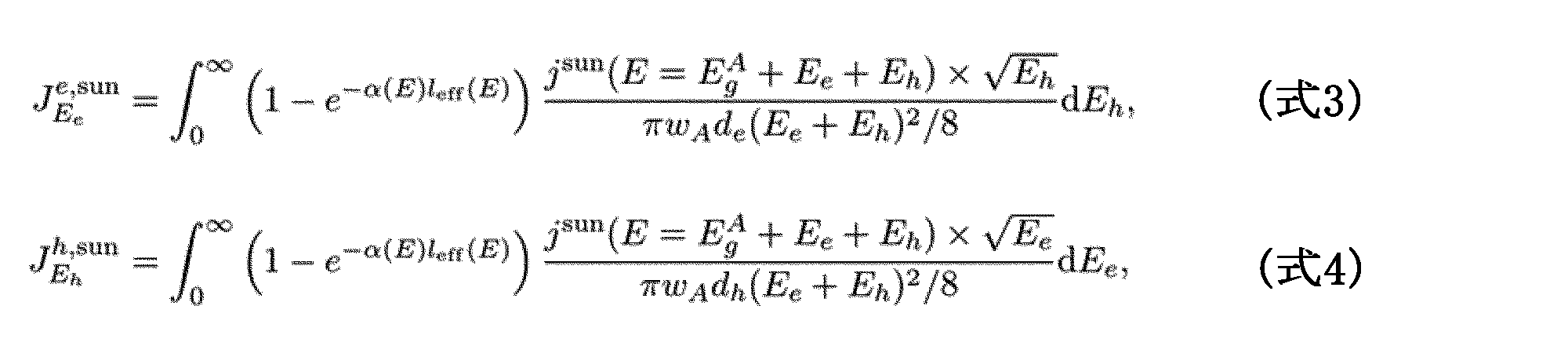
ここで、α(E)はエネルギーEにおける吸収層の光吸収係数、leff(E)は吸収層内における入射光の実効的な光路長であり、表面テクスチャ等がない場合は吸収層厚さwAに等しく、表面テクスチャが施された場合、理想的な条件、つまり上述したヤブロノビッチ限界においては吸収層の屈折率をn(E)としてleff(E)=4(n(E))2wAとなる。吸収層のエネルギーギャップをEg
Aとし、電子及び正孔の有効質量をそれぞれme
*、mh
*とした。単位体積当たりの電子及び正孔の状態密度をそれぞれDe(Ee)=de×(Ee)1/2、Dh(Eh)=dh×(Eh)1/2とした。入射された太陽光スペクトル(単位時間単位面積当たりに入射するエネルギーEにおける光子数エネルギー密度は、大気通過量(Air Mass)が0(零)の条件下の黒体輻射スペクトルにより以下のように近似した。

ここでCRは集光倍率、cは真空中の光速、RSは太陽の半径、LESは太陽と地球の平均距離、D0
γ(E)=E2/(π2h3c3)は真空中におけるエネルギーEをもつ光の単位体積当たりの状態密度、hはプランク定数/(2π)、Tsは太陽の表面温度、kBはボルツマン定数である。
電子・正孔の再結合損失レート(式1および式2の第1等号の右辺第2項)は、それぞれ、以下の式6および式7で表される。

電子・正孔の電極への取り出しレート(式1および式2の第1等号の右辺第3項)は、それぞれ、以下の式8および式9で表される。

ここでτoutはキャリア取り出し時間、Eg
Xはフィルタ層のエネルギーギャップとする。θ(z)はz>0で1となる階段関数である。電子側、正孔側の電極における分布関数は、環境温度Tc、フェルミエネルギーμをそれぞれμc, -μvとした以下の式10のフェルミ分布関数により与えられる。

ここで、電子側および正孔側の電極におけるフェルミエネルギーの差は太陽電池における動作電圧Vとの関係は以下の式11によって表される。

ここでqは電気素量である。
電子・正孔のバンド内熱緩和レート(式1および2の第1等号の右辺第4項)は、以下の式12で表される。

ここで、We(h)
Ei,Ef は電子(正孔)バンドにおいて、エネルギーEiをもつ始状態からEfをもつ終状態への散乱、あるいはその逆過程に関するキャリアのフォノン散乱強度を与えるパラメータである。この具体的な表式は、吸収層と関与するフォノンの種類などを指定することにより決定される。吸収層のシリコンに対する数値計算においては、LAフォノンをフォノン緩和の要因として取り入れた。fB
Tphは格子温度Tphにおけるフォノンの分布関数(ボースアインシュタイン分布)であり、以下の式13で与えられる。

以上により、吸収層のバンド内のすべてのエネルギーを持つキャリアの分布関数ne
Ee、nh
Ehに関して閉じたレート方程式(式1および式2)が得られた。これを定常条件のもとで解くことで、一定の太陽光照射時において吸収層内で実現されるキャリアのエネルギー分布関数が得られる。
<2.電池の変換効率、開放電圧およびエネルギー流の計算>
体積Ω=S(表面積)×wA(厚さ)の吸収層から、電極へと取り出される電流Iは以下の式14で与えられる。

ここで、Je,out
Ee,およびJh,out
Eh は式8および式9ですでに求めたキャリア分布関数を用いることで電流を評価することができる。これより、取り出される単位面積当たりの電力PWORKは以下の式15で与えられる。

体積Ω=S(表面積)×wA(厚さ)の吸収層から、電極へと取り出される電流Iは以下の式14で与えられる。
一方、単位面積あたりに入射する太陽光エネルギーPSUNは、以下の式16で与えられる。

太陽電池のエネルギー変換効率ηはこれらを用いて、以下の式17により求められる。

本実施形態の太陽電池10に関係するエネルギー流は、上述した太陽光入射エネルギー流PSUN および電力として取り出される仕事PWORK に加えて、4つのエネルギー流がある。PTは吸収層11に吸収されずに透過損失となる透過エネルギー流、PRadは 吸収層11における発光再結合による輻射再結合損失のエネルギー流、PQoutは電極12,13へ排出される熱エネルギー流、PQinは吸収層11の格子へ排出されるエネルギー流である。これらはエネルギー保存則PSUN = PT + PRad + PQout +PQin +PWORK により関係している。
透過エネルギー流PTは、以下の式18により与えられる。

単位面積当たりの輻射再結合損失PRadは、以下の式19により与えられる。

ここで、〈nenh〉E はE=Ee+Eh+Eg
Aを満たすような電子正孔対のすべての組み合わせについてその分布関数の積ne
Ee×nh
Ehの平均値をとったものである。したがって、これも吸収層内の分布関数が微視的レート方程式の定常解により得られているので、評価することができる。
電極へ排出される熱エネルギー流PQoutは以下の式20で与えられる。これも吸収層内の分布関数が微視的レート方程式の定常解を用いて評価することができる。

以上の式15、式16、式18~式20およびエネルギー保存則により吸収層格子へ排出されるエネルギー流(単位時間および単位面積当たり)は、以下の式21により計算される。

上述した式11と吸収層内の電荷中性条件、すなわち電子と正孔の総数が等しいという条件から、第1電極と第2電極の化学ポテンシャルは電圧Vの関数として、それぞれ式22、式23で与えられる。

式22および式23は以下のようにして求められる。式1および式2において総電荷数の単位時間当たりの変化に寄与する項は、それぞれ式8および式9となる。単位時間当たりの吸収層から電極(電子側)への電子流出数は式14の第2等式左辺により、単位時間当たりの吸収層から電極(正孔側)への正孔流出数は式14の第2等式右辺により与えられ式(14)の第2等式が成立する限り、吸収層から流れ出る電子と正孔の総数が等しく吸収層内で総電荷の時間的変動がない状況が実現する。式14の第2等式に式8および式9を代入すると以下の式24が得られる。

ここでΔEg≡(Eg
X-ΔEg
A)/2と定義した。式24は、吸収層の中から電極へ単位時間当たりに流れ出る総電荷数を意味する左辺と、電極から吸収層に単位時間当たりに入ってくる総電荷数を意味する右辺がバランスすることで、単に吸収層内の正味の総電荷数が時間的に変動しないことを意味するのである。式24に電極から吸収層へ単位時間当たりに入りこむ総電荷数がゼロになるための条件として式24の右辺を0(ゼロ)と課すことで以下の式25が得られる。

太陽電池動作においては、式10で与えられるフェルミ分布関数が1より十分小さく、ボルツマン分布で近似できるとして、以下の式26が得られる。

並びに、状態密度のエネルギー依存性De
E=de×(E)1/2、Dh
E=dh×(E)1/2を式25に代入すると、以下の式27が得られる。

式27の左辺において一つ目の括弧の中身は正でありゼロとなり得ないことから、式27が成立する条件は、二つ目の括弧の中身がゼロになることであるので、以下の式28が得られる。

式28の両辺の自然対数をとることで以下の式29が得られる。

この式29は、吸収層内が総電荷数を固定(ここではゼロ=電荷中性)するための条件として、電子側電極と正孔側電極における化学ポテンシャルの関係を規定する。式29と式11から式22および式23が得られる。すなわち、吸収層内の電荷中性条件の下で、電位差Vの関数として各電極における化学ポテンシャルは式22および式23で与えられる。
電圧Vおよび設定パラメータ、例えばフィルタ層のエネルギーギャップ、キャリア取り出し時間、吸収層温度、集光倍率を与え、各生成または損失レートの式3、式4、式6、式7、式8,式9、式12を代入すれば、レート方程式(式1および式2の各第2等式)において、未知変数である、全てのエネルギーEeおよびEhに関する分布関数ne
Eeおよびnh
Ehが残り、その他の項はすべて定数として与えられる。すなわち、全てのエネルギーEe,およびEhに関して、式1および式2のレート方程式を書き下せば、分布関数ne
Eeとnh
Ehについて解くべき、閉じた多変数の非線形連立方程式が確定する。これを数値的に、例えばニュートン法を用いて解くことで全てのエネルギーEeおよびEhに関する分布関数ne
Eeおよびnh
Ehを、電圧Vやその他の設定パラメータの関数として求めることができる。
このようにして求められた吸収層内キャリアの分布関数を用いることにより、式8を式15に、式5を式16に代入し、それらにレート方程式の解として決定した分布関数の値を代入する。これにより得られるPWORKとPSUNを式17に代入し、変換効率ηを様々な動作電圧Vに対して求めた。さらに、フィルタ層のエネルギーギャップ、キャリア取り出し時間、吸収層温度、集光倍率などを変えながら各条件ごとの最大変換効率や開放電圧を求めた。
図9は、本発明の一実施形態に係る太陽電池の変換効率を取り出し電圧に対して各フィルタ層のエネルギーギャップでシミュレーションによって求めた図である。このシミュレーションでは、図1に示す第1フィルタ層14と第2フィルタ層15とは同一の半導体材料を用いており(以下、単に「フィルタ層」と称する。)、吸収層11はシリコン(Eg
A=1.12eV)を用いており、吸収層11の厚さwAを10μm、大気通過係数(AM)は0、太陽の表面温度Tsは6000K、電極温度Tcは300K、吸収層の温度TPHは450K、吸収層11から第1電極12および第2電極13へのキャリア取り出し時間τoutは100ns(ナノ秒)、吸収層11におけるフォノン緩和時間(熱化時間)は1ps(ピコ秒)程度とした。
図9を参照するに、フィルタ層のエネルギーギャップEg
Xが吸収層のシリコンのエネルギーギャップEg
Aである1.12eVよりも大きいと変換効率の最大値が29.5%を超え、Eg
Aが1.3eVおよび1.7eVでは、30%台であることが分かる。
図10は、本発明の一実施形態に係る太陽電池の最大変換効率をフィルタ層のエネルギーギャップに対して各温度でシミュレーションによって求めた図である。図10は、図9と同様のシミュレーションを吸収層の温度を変えて行い、横軸をフィルタ層のエネルギーギャップEg
X、縦軸を変換効率の最大値ηmaxとしてプロットしたものである。
図10を参照するに、吸収層の温度TPHが300K、つまり、TPH=Tcの場合、フィルタ層のエネルギーギャップEg
Xが大きくなるにしたがって、最大変換効率が低下することが分かる。これに対して、TPHが375Kおよび450Kの場合、最大変換効率は、シリコンのエネルギーギャップEg
Aの1.12eV以下では29.5%よりも低いが、Eg
Aの1.12eVよりも大きい1.3eVでは増加していることが分かる。TPHが375Kの場合は1.70eV以下では30%を超えており、TPHが450Kの場合は1.87eV以下では30%を超えていることが分かる。
図11は、本発明の一実施形態に係る太陽電池の開放電圧をフィルタ層のエネルギーギャップに対して各温度でシミュレーションによって求めた図である。図11は、図9と同様のシミュレーションを吸収層の温度を変えて行い、横軸をフィルタ層のエネルギーギャップEg
X、縦軸を開放電圧VOCとしてプロットしたものである。
図11を参照するに、TPHが375Kおよび450Kの場合は、開放電圧VOCは、シリコンのエネルギーギャップEg
Aの1.12eV以下では、0.92eVで一定であるが、Eg
Aの1.12eVよりも大きいエネルギーギャップEg
Xでは、Eg
Xの増加にしたがって開放電圧VOCは増加していることが分かる。また、TPHが375Kと450Kとを比較すると、450Kの方が開放電圧VOCが高くなっている。このことは、図3で説明したように、吸収層11のキャリアのエネルギーが増加し、キャリア分布Nc
Aが高エネルギー側にシフトし、フィルタ層14のエネルギーギャップEg
Xよりも大きいエネルギーを有するキャリアが吸収層11から電極12に流出することにより生じている。これは正孔についても同様である。
<3.エネルギー流を用いた太陽電池動作の安定性評価>
本実施形態の太陽電池は、吸収層の格子温度TPHが電極温度TC(例えば300K)よりも高い場合に変換効率の上昇という効果が得られる。TPH>TCは、吸収層の格子温度TPHを上昇させる熱流により実現できる。入射する太陽光の光エネルギーの一部が吸収層を温める熱流となり回収され(すなわち「熱回収型」)、それにより太陽光以外の熱流の供給がない場合でも本実施形態の太陽電池の動作が行われる実施例を以下に説明する。
本実施形態の太陽電池は、吸収層の格子温度TPHが電極温度TC(例えば300K)よりも高い場合に変換効率の上昇という効果が得られる。TPH>TCは、吸収層の格子温度TPHを上昇させる熱流により実現できる。入射する太陽光の光エネルギーの一部が吸収層を温める熱流となり回収され(すなわち「熱回収型」)、それにより太陽光以外の熱流の供給がない場合でも本実施形態の太陽電池の動作が行われる実施例を以下に説明する。
入射太陽光から吸収層格子へ流入する熱流PQinは、上記の式21において計算され、PQinが正となる場合には吸収層格子を温めることができる。吸収層格子の温度TPHの上昇分ΔTPH=TPH-TC(K)の平均値はPQinを用いて以下の式30により与えられる。

ここで、L、D、wAは、それぞれ、先の図4に示した第1フィルタ層141,2および第2フィルタ層151,2(すなわち、第1電極121,2および第2電極131,2)の間隔L1とL2が同じ場合の間隔L、幅D1とD2が同じ場合の幅D、吸収層11の厚さwAであり、κは吸収層11の面内方向の熱伝導度である。この平均温度の上昇分が、すでに仮定している値(TPH-TC)と一致する場合に、太陽光のみにより本実施例の太陽電池が安定して自立的に機能することになる。なお、PQinが正であれば、仮定している温度上昇をどのように与えても、式30を満たすようにL、D、wA、κを選べば、そのような安定動作を得ることができる。
本実施例の太陽電池が安定的に動作する条件を満たす場合において吸収層の平均温度上昇分を電極の間隔に対して求めた。取り出し時間τout、吸収層の温度TPH、電極の温度Tc、集光倍率CRおよびフィルタ層のエネルギーギャップEg
Xを下記の表1のように設定し、上記式21の計算から吸収層格子へ排出される熱流PQinを算出した。この熱流PQinによる温度上昇分は、表1に示すTPHとTcとの差と一致するように式30から間隔Lが選択される。このエネルギー流と間隔Lを表1に示した。なお、式30において、間隔Lは幅Dよりも十分大きく(L>>D)、光吸収については、理想的なテクスチャリングが施されたとして、先に述べたヤブロノビッチ限界を採用した。厚さwAは10μm、吸収層11の面内方向の熱伝導率κを1W/(m・K)とした。

図12は、実施例の太陽電池が安定的に動作する条件を満たす吸収層の平均温度上昇分と電極の間隔との関係を示す図である。図12を参照するに、本実施例の太陽電池が上記の式30を満たす安定的に動作する条件を表1の3つの条件に対して示した。
この結果によれば、τoutが100ns、CRが1の場合、Eg
Xが1.6eVの条件#1では、間隔Lが6.6mmのときに平均温度上昇分が75Kになり、Eg
Xが1.7eVの条件2では、間隔Lが11.8mmのときに平均温度上昇分が150Kになることが分かる。また、τoutが10ns、CRが10の場合、Eg
Xが1.8eVの条件#3では、間隔Lが8.2mmの場合に平均温度上昇分が150Kとなり安定動作することが分かる。さらに、表1に示されるように、上記条件#1~#3のいずれにおいても、30%を超える高い変換効率ηが得られることが分かる。
また、先の図6で示した実施形態の太陽電池40において、入射した太陽光が吸収層11に吸収されずに透過損失となる透過エネルギー流PTを赤外線吸収層42により吸収し、その熱によい吸収層11を加熱する場合は、最大で全ての透過分を赤外吸収層42が吸収したとすると、平均温度上昇分は、以下の式31で見積られる。

この式31から明らかなように、吸収層11を透過する太陽光を赤外線吸収層42で吸収することで、吸収層11の平均温度上昇分を増加できる。これにより、先の図3で説明したように、吸収層11の温度TPHの上昇によって吸収層11のキャリアのエネルギーが増加し、キャリア分布Nc
Aが高エネルギー側にシフトすることで、太陽電池の開放電圧が上昇し、変換効率が向上する。また、この場合は、表1の場合、つまり赤外線吸収層42を用いない場合に比べて、より短い距離Lで安定動作が実現できる。
以上、本発明の実施形態および実施例について詳述したが、本発明は係る特定の実施形態および実施例に限定されるものではなく、請求の範囲に記載された本発明の範囲内において、種々の変形・変更が可能である。
なお、以上の説明に関してさらに実施形態として以下の付記を開示する。
(付記1) 発電のために熱を利用する太陽電池であって、
受光により第1および第2のキャリアを生成する半導体材料を有する吸収層と、
前記吸収層の上に設けられた第1および第2の電極と、
前記吸収層と前記第1の電極との間に設けられ、第1のキャリアが前記吸収層から前記第1の電極への移動を制御する第1のフィルタ層と、
前記吸収層と前記第2の電極との間に設けられ、第2のキャリアが前記吸収層から前記第2の電極への移動を制御する第2のフィルタ層と、
を備え、
前記第1および第2のフィルタ層は半導体材料からなり、そのエネルギーギャップが前記吸収層のエネルギーギャップよりも大きく、
前記熱によって前記吸収層の温度を上昇させ、前記第1および第2の電極の温度よりも高くすることによって当該太陽電池の変換効率を向上可能である、前記太陽電池。
(付記2) 前記熱は、前記吸収層が太陽光の受光により発生する熱である、付記1記載の太陽電池。
(付記3) 前記吸収層に前記熱を供給する加熱手段をさらに備える、付記1または2記載の太陽電池。
(付記4) 前記加熱手段は、前記吸収層に接して配置される赤外線吸収層である、付記3記載の太陽電池。
(付記5) 前記加熱手段は、当該太陽電池の外部から導入する熱を利用する、付記3記載の太陽電池。
(付記6) 前記吸収層の温度は、前記第1および第2の電極の温度よりも高い、請求項1~5のうちいずれか一項記載の太陽電池。
(付記7) 前記吸収層の前記温度が上昇するにしたがって、前記吸収層の前記第1および第2のキャリアのエネルギー分布が高エネルギー方向に変化し、前記吸収層から前記第1および第2の電極にそれぞれ流出する前記第1および第2のキャリアのエネルギーが、前記第1および第2の電極からそれぞれ前記吸収層に流入する第1および第2のキャリアのエネルギーよりも大きい、付記1~6のうちいずれか一項記載の太陽電池。
(付記8) 前記第1のフィルタ層および電極と前記第2のフィルタ層および電極とは、前記吸収層の光が照射される第1の面に配置される、付記1~7のうちいずれか一項記載の太陽電池。
(付記9) 前記第1のフィルタ層および電極と前記第2のフィルタ層および電極とは、前記吸収層の光が照射される第1の面とは反対側の第2の面に配置される、付記1~7のうちいずれか一項記載の太陽電池。
(付記10) 第1のフィルタ層および電極と前記第2のフィルタ層および電極とは、前記吸収層の光が照射される第1の面に配置され、さらに、該第1の面とは反対側の第2の面に配置される、付記1~7のうちいずれか一項記載の太陽電池。
(付記11) 前記第1のフィルタ層および電極は、前記吸収層の光が照射される第1の面および該第1の面とは反対側の第2の面のいずれか一方の面に配置され、前記第2のフィルタ層および前記第2の電極は他方の面に配置される、付記1~7のうちいずれか一項記載の太陽電池。
(付記12) 前記第1のフィルタ層および電極と前記第2のフィルタ層および電極とは、前記吸収層を挟んで、前記吸収層の層内方向に離隔して配置される、付記11記載の太陽電池。
(付記13) 前記第1のフィルタ層および電極と前記第2のフィルタ層および電極とは、前記吸収層を挟んで対向して配置される、付記11記載の太陽電池。
(付記14) 前記第1のフィルタ層および電極と前記第2のフィルタ層および電極とは、前記吸収層の第1または第2の面内の一方向に所定の距離だけ離隔して配置され、該距離は、該一方向の前記第1および第2のフィルタ層の幅よりも大きい、付記1~13のうちいずれか一項記載の太陽電池。
(付記15) 前記吸収層の光が照射される第1の面とは反対側の第2の面に接して赤外線吸収層をさらに備える、付記8~14のうちいずれか一項記載の太陽電池。
(付記16) 前記吸収層は、厚さ方向に延びる複数の孔部が周期的に配列された第1の半導体層と第2の半導体層を有し、該第1の半導体層と第2の半導体層とが、それぞれの孔部が対向しないように積層されてなる、付記1~15のうちいずれか一項記載の太陽電池。
(付記17) 前記隣接する孔部は互いに1μm以下の間隔をもって配置される、付記16記載の太陽電池。
(付記18) 前記孔部の内径が1μm以下である、付記16または17記載の太陽電池。
(付記19) 前記吸収層は、前記第1のフィルタ層に接触する部分にn型ドープ領域を有し、前記第2のフィルタ層に接触する部分にp型ドープ領域を有する、付記1~18のうちいずれか一項記載の太陽電池。
(付記20) 前記第1のフィルタ層はn型ドープされてなり、前記第2のフィルタ層はp型ドープされてなる、付記1~19のうちいずれか一項記載の太陽電池。
(付記21) 前記第1の電極はn型ドープされた半導体材料からなり、前記第2の電極はp型ドープされた半導体材料からなる、付記1~20のうちいずれか一項記載の太陽電池。
(付記22) 前記吸収層と第1のフィルタ層との間、前記吸収層と第2のフィルタ層との間、前記第1のフィルタ層と第1の電極との間、および第2のフィルタ層と第2の電極との少なくともいずれかに絶縁層をさらに備える、付記1~21のうちいずれか一項記載の太陽電池。
(付記23) 発電のために熱を利用する太陽電池の製造方法であって、
第1の半導体材料の吸収層を形成するステップと、
前記吸収層の表面にパッシベーション層を形成するステップと、
前記パッシベーション層の一部を除去して吸収層の表面を露出するステップと、
前記露出した吸収層の表面に、第2の半導体材料の第1のフィルタ層および第2のフィルタ層を離隔して形成するステップであって、該第2の半導体材料のエネルギーギャップが前記第1の半導体材料のエネルギーギャップよりも高い、該ステップと、
前記第1および第2フィルタ層の上に、それぞれ第1の電極および第2の電極を形成するステップと、を含み、
前記熱によって前記吸収層の温度を上昇させ、前記第1および第2の電極の温度よりも高くすることによって当該太陽電池の変換効率を向上可能である、前記製造方法。
(付記1) 発電のために熱を利用する太陽電池であって、
受光により第1および第2のキャリアを生成する半導体材料を有する吸収層と、
前記吸収層の上に設けられた第1および第2の電極と、
前記吸収層と前記第1の電極との間に設けられ、第1のキャリアが前記吸収層から前記第1の電極への移動を制御する第1のフィルタ層と、
前記吸収層と前記第2の電極との間に設けられ、第2のキャリアが前記吸収層から前記第2の電極への移動を制御する第2のフィルタ層と、
を備え、
前記第1および第2のフィルタ層は半導体材料からなり、そのエネルギーギャップが前記吸収層のエネルギーギャップよりも大きく、
前記熱によって前記吸収層の温度を上昇させ、前記第1および第2の電極の温度よりも高くすることによって当該太陽電池の変換効率を向上可能である、前記太陽電池。
(付記2) 前記熱は、前記吸収層が太陽光の受光により発生する熱である、付記1記載の太陽電池。
(付記3) 前記吸収層に前記熱を供給する加熱手段をさらに備える、付記1または2記載の太陽電池。
(付記4) 前記加熱手段は、前記吸収層に接して配置される赤外線吸収層である、付記3記載の太陽電池。
(付記5) 前記加熱手段は、当該太陽電池の外部から導入する熱を利用する、付記3記載の太陽電池。
(付記6) 前記吸収層の温度は、前記第1および第2の電極の温度よりも高い、請求項1~5のうちいずれか一項記載の太陽電池。
(付記7) 前記吸収層の前記温度が上昇するにしたがって、前記吸収層の前記第1および第2のキャリアのエネルギー分布が高エネルギー方向に変化し、前記吸収層から前記第1および第2の電極にそれぞれ流出する前記第1および第2のキャリアのエネルギーが、前記第1および第2の電極からそれぞれ前記吸収層に流入する第1および第2のキャリアのエネルギーよりも大きい、付記1~6のうちいずれか一項記載の太陽電池。
(付記8) 前記第1のフィルタ層および電極と前記第2のフィルタ層および電極とは、前記吸収層の光が照射される第1の面に配置される、付記1~7のうちいずれか一項記載の太陽電池。
(付記9) 前記第1のフィルタ層および電極と前記第2のフィルタ層および電極とは、前記吸収層の光が照射される第1の面とは反対側の第2の面に配置される、付記1~7のうちいずれか一項記載の太陽電池。
(付記10) 第1のフィルタ層および電極と前記第2のフィルタ層および電極とは、前記吸収層の光が照射される第1の面に配置され、さらに、該第1の面とは反対側の第2の面に配置される、付記1~7のうちいずれか一項記載の太陽電池。
(付記11) 前記第1のフィルタ層および電極は、前記吸収層の光が照射される第1の面および該第1の面とは反対側の第2の面のいずれか一方の面に配置され、前記第2のフィルタ層および前記第2の電極は他方の面に配置される、付記1~7のうちいずれか一項記載の太陽電池。
(付記12) 前記第1のフィルタ層および電極と前記第2のフィルタ層および電極とは、前記吸収層を挟んで、前記吸収層の層内方向に離隔して配置される、付記11記載の太陽電池。
(付記13) 前記第1のフィルタ層および電極と前記第2のフィルタ層および電極とは、前記吸収層を挟んで対向して配置される、付記11記載の太陽電池。
(付記14) 前記第1のフィルタ層および電極と前記第2のフィルタ層および電極とは、前記吸収層の第1または第2の面内の一方向に所定の距離だけ離隔して配置され、該距離は、該一方向の前記第1および第2のフィルタ層の幅よりも大きい、付記1~13のうちいずれか一項記載の太陽電池。
(付記15) 前記吸収層の光が照射される第1の面とは反対側の第2の面に接して赤外線吸収層をさらに備える、付記8~14のうちいずれか一項記載の太陽電池。
(付記16) 前記吸収層は、厚さ方向に延びる複数の孔部が周期的に配列された第1の半導体層と第2の半導体層を有し、該第1の半導体層と第2の半導体層とが、それぞれの孔部が対向しないように積層されてなる、付記1~15のうちいずれか一項記載の太陽電池。
(付記17) 前記隣接する孔部は互いに1μm以下の間隔をもって配置される、付記16記載の太陽電池。
(付記18) 前記孔部の内径が1μm以下である、付記16または17記載の太陽電池。
(付記19) 前記吸収層は、前記第1のフィルタ層に接触する部分にn型ドープ領域を有し、前記第2のフィルタ層に接触する部分にp型ドープ領域を有する、付記1~18のうちいずれか一項記載の太陽電池。
(付記20) 前記第1のフィルタ層はn型ドープされてなり、前記第2のフィルタ層はp型ドープされてなる、付記1~19のうちいずれか一項記載の太陽電池。
(付記21) 前記第1の電極はn型ドープされた半導体材料からなり、前記第2の電極はp型ドープされた半導体材料からなる、付記1~20のうちいずれか一項記載の太陽電池。
(付記22) 前記吸収層と第1のフィルタ層との間、前記吸収層と第2のフィルタ層との間、前記第1のフィルタ層と第1の電極との間、および第2のフィルタ層と第2の電極との少なくともいずれかに絶縁層をさらに備える、付記1~21のうちいずれか一項記載の太陽電池。
(付記23) 発電のために熱を利用する太陽電池の製造方法であって、
第1の半導体材料の吸収層を形成するステップと、
前記吸収層の表面にパッシベーション層を形成するステップと、
前記パッシベーション層の一部を除去して吸収層の表面を露出するステップと、
前記露出した吸収層の表面に、第2の半導体材料の第1のフィルタ層および第2のフィルタ層を離隔して形成するステップであって、該第2の半導体材料のエネルギーギャップが前記第1の半導体材料のエネルギーギャップよりも高い、該ステップと、
前記第1および第2フィルタ層の上に、それぞれ第1の電極および第2の電極を形成するステップと、を含み、
前記熱によって前記吸収層の温度を上昇させ、前記第1および第2の電極の温度よりも高くすることによって当該太陽電池の変換効率を向上可能である、前記製造方法。
10、20、30~36、40、50 太陽電池
11、51、 吸収層
12、121、122 第1電極
13、131、132 第2電極
14、141、142 第1フィルタ層
15、151、152 第2フィルタ層
16、161、162 第1積層体
17、171、172 第2積層体
42 赤外線吸収層
51a 第1半導体層
51b 第2半導体層
11、51、 吸収層
12、121、122 第1電極
13、131、132 第2電極
14、141、142 第1フィルタ層
15、151、152 第2フィルタ層
16、161、162 第1積層体
17、171、172 第2積層体
42 赤外線吸収層
51a 第1半導体層
51b 第2半導体層
Claims (13)
- 発電のために熱を利用する太陽電池であって、
受光により第1および第2のキャリアを生成する半導体材料を有する吸収層と、
前記吸収層の上に設けられた第1および第2の電極と、
前記吸収層と前記第1の電極との間に設けられ、第1のキャリアが前記吸収層から前記第1の電極への移動を制御する第1のフィルタ層と、
前記吸収層と前記第2の電極との間に設けられ、第2のキャリアが前記吸収層から前記第2の電極への移動を制御する第2のフィルタ層と、
を備え、
前記第1および第2のフィルタ層は半導体材料からなり、そのエネルギーギャップが前記吸収層のエネルギーギャップよりも大きく、
前記熱によって前記吸収層の温度を上昇させ、前記第1および第2の電極の温度よりも高くすることによって当該太陽電池の変換効率を向上可能である、前記太陽電池。 - 前記熱は、前記吸収層が太陽光の受光により発生する熱である、請求項1記載の太陽電池。
- 前記吸収層に前記熱を供給する加熱手段をさらに備える、請求項1または2記載の太陽電池。
- 前記加熱手段は、前記吸収層に接して配置される赤外線吸収層である、請求項3記載の太陽電池。
- 前記加熱手段は、当該太陽電池の外部から導入する熱を利用する、請求項3記載の太陽電池。
- 前記吸収層の温度は、前記第1および第2の電極の温度よりも高い、請求項1~5のうちいずれか一項記載の太陽電池。
- 前記吸収層の前記温度が上昇するにしたがって、前記吸収層の前記第1および第2のキャリアのエネルギー分布が高エネルギー方向に変化し、前記吸収層から前記第1および第2の電極にそれぞれ流出する前記第1および第2のキャリアのエネルギーが、前記第1および第2の電極からそれぞれ前記吸収層に流入する第1および第2のキャリアのエネルギーよりも大きい、請求項1~6のうちいずれか一項記載の太陽電池。
- 前記第1のフィルタ層および電極と前記第2のフィルタ層および電極とは、前記吸収層の第1または第2の面内の一方向に所定の距離だけ離隔して配置され、該距離は、該一方向の前記第1および第2のフィルタ層の厚さよりも大きい、請求項1~7のうちいずれか一項記載の太陽電池。
- 前記吸収層は、厚さ方向に延びる複数の孔部が周期的に配列された第1の半導体層と第2の半導体層を有し、該第1の半導体層と第2の半導体層とが、それぞれの孔部が対向しないように積層されてなる、請求項1~8のうちいずれか一項記載の太陽電池。
- 前記隣接する孔部は互いに1μm以下の間隔をもって配置される、請求項9記載の太陽電池。
- 前記孔部の内径が1μm以下である、請求項9または10記載の太陽電池。
- 前記吸収層は、前記第1のフィルタ層に接触する部分にn型ドープ領域を有し、前記第2のフィルタ層に接触する部分にp型ドープ領域を有する、請求項1~11のうちいずれか一項記載の太陽電池。
- 前記第1のフィルタ層と前記第1の電極との間および前記第2のフィルタ層と前記第2の電極との間の少なくとも一方に絶縁層をさらに備える、請求項1~12のうちいずれか一項記載の太陽電池。
Applications Claiming Priority (2)
| Application Number | Priority Date | Filing Date | Title |
|---|---|---|---|
| JP2017241808A JP2019110192A (ja) | 2017-12-18 | 2017-12-18 | 太陽電池 |
| JP2017-241808 | 2017-12-18 |
Publications (1)
| Publication Number | Publication Date |
|---|---|
| WO2019124012A1 true WO2019124012A1 (ja) | 2019-06-27 |
Family
ID=66994733
Family Applications (1)
| Application Number | Title | Priority Date | Filing Date |
|---|---|---|---|
| PCT/JP2018/043782 Ceased WO2019124012A1 (ja) | 2017-12-18 | 2018-11-28 | 太陽電池 |
Country Status (2)
| Country | Link |
|---|---|
| JP (1) | JP2019110192A (ja) |
| WO (1) | WO2019124012A1 (ja) |
Cited By (1)
| Publication number | Priority date | Publication date | Assignee | Title |
|---|---|---|---|---|
| CN115720451A (zh) * | 2021-08-23 | 2023-02-28 | 天光材料科技股份有限公司 | 光二极管的结构 |
Citations (7)
| Publication number | Priority date | Publication date | Assignee | Title |
|---|---|---|---|---|
| JPS62163973U (ja) * | 1986-04-08 | 1987-10-17 | ||
| JPH09283778A (ja) * | 1996-02-28 | 1997-10-31 | Hitachi Ltd | 太陽電池 |
| JP2001085712A (ja) * | 1999-09-17 | 2001-03-30 | Oki Electric Ind Co Ltd | 太陽電池 |
| JP2009059915A (ja) * | 2007-08-31 | 2009-03-19 | Toyota Central R&D Labs Inc | 光起電力素子 |
| JP2010219240A (ja) * | 2009-03-16 | 2010-09-30 | Panasonic Electric Works Co Ltd | 有機太陽電池 |
| JP2017143174A (ja) * | 2016-02-10 | 2017-08-17 | 株式会社リコー | 光電変換装置 |
| US20170338766A1 (en) * | 2013-06-11 | 2017-11-23 | Mark W. Miles | Hybrid flow solar thermal collector |
Family Cites Families (4)
| Publication number | Priority date | Publication date | Assignee | Title |
|---|---|---|---|---|
| DE102013105462A1 (de) * | 2013-05-28 | 2014-12-04 | Ernst-Abbe-Fachhochschule Jena | Schichtenfolge zur photoelektrischen Umwandlung von Licht sowie Hot Carrier Solarzelle |
| US20150236175A1 (en) * | 2013-12-02 | 2015-08-20 | Solexel, Inc. | Amorphous silicon passivated contacts for back contact back junction solar cells |
| US9825191B2 (en) * | 2014-06-27 | 2017-11-21 | Sunpower Corporation | Passivation of light-receiving surfaces of solar cells with high energy gap (EG) materials |
| US10079319B2 (en) * | 2015-12-16 | 2018-09-18 | Sunpower Corporation | Solar cell fabrication using laser patterning of ion-implanted etch-resistant layers and the resulting solar cells |
-
2017
- 2017-12-18 JP JP2017241808A patent/JP2019110192A/ja active Pending
-
2018
- 2018-11-28 WO PCT/JP2018/043782 patent/WO2019124012A1/ja not_active Ceased
Patent Citations (7)
| Publication number | Priority date | Publication date | Assignee | Title |
|---|---|---|---|---|
| JPS62163973U (ja) * | 1986-04-08 | 1987-10-17 | ||
| JPH09283778A (ja) * | 1996-02-28 | 1997-10-31 | Hitachi Ltd | 太陽電池 |
| JP2001085712A (ja) * | 1999-09-17 | 2001-03-30 | Oki Electric Ind Co Ltd | 太陽電池 |
| JP2009059915A (ja) * | 2007-08-31 | 2009-03-19 | Toyota Central R&D Labs Inc | 光起電力素子 |
| JP2010219240A (ja) * | 2009-03-16 | 2010-09-30 | Panasonic Electric Works Co Ltd | 有機太陽電池 |
| US20170338766A1 (en) * | 2013-06-11 | 2017-11-23 | Mark W. Miles | Hybrid flow solar thermal collector |
| JP2017143174A (ja) * | 2016-02-10 | 2017-08-17 | 株式会社リコー | 光電変換装置 |
Non-Patent Citations (1)
| Title |
|---|
| KAMIDE, K. ET AL.: "Nonequilibrium theory of solar cells including finite thermalization and extraction time", 78TH JSAP AUTUMN MEETING, 6 September 2017 (2017-09-06), pages 14-052 * |
Cited By (1)
| Publication number | Priority date | Publication date | Assignee | Title |
|---|---|---|---|---|
| CN115720451A (zh) * | 2021-08-23 | 2023-02-28 | 天光材料科技股份有限公司 | 光二极管的结构 |
Also Published As
| Publication number | Publication date |
|---|---|
| JP2019110192A (ja) | 2019-07-04 |
Similar Documents
| Publication | Publication Date | Title |
|---|---|---|
| Gamal et al. | Design of lead-free perovskite solar cell using Zn1-xMgxO as ETL: SCAPS device simulation | |
| Moon et al. | Design and simulation of FeSi2‐based novel heterojunction solar cells for harnessing visible and near‐infrared light | |
| Srivastava et al. | Theoretical study of perovskite solar cell for enhancement of device performance using SCAPS-1D | |
| Du et al. | Device simulation of lead-free CH3NH3SnI3 perovskite solar cells with high efficiency | |
| Park et al. | Lossless hybridization between photovoltaic and thermoelectric devices | |
| US8895839B2 (en) | Multijunction photovoltaic device | |
| Rahman et al. | Numerical modeling and extensive analysis of an extremely efficient RbGeI 3-based perovskite solar cell by incorporating a variety of ETL and HTL materials to enhance PV performance | |
| Maurya et al. | Efficient Sb2Se3 solar cell with a higher fill factor: A theoretical approach based on thickness and temperature | |
| US20100258164A1 (en) | Photovoltaic force device | |
| EP1875517A1 (de) | Heterokontaktsolarzelle mit invertierter schichtstrukturgeometrie | |
| Rani et al. | Opto-electrical modeling of CsPbBr3 based all-inorganic perovskite solar cell | |
| Dakua et al. | Analysis of various hole transport layers (HTLs) on the performance of CZTS-solar cell | |
| Shahadath et al. | Optimization of high efficiency lead-free double perovskite Dy 2 NiMnO 6 (DNMO) for optimal solar cell and renewable energy applications: a numerical SCAPS-1D simulation | |
| Chargui et al. | Improving CZTS/ZTO solar cell efficiency with inorganic BSF layers | |
| Kareem et al. | CHTS/Zn2P3-based solar cells with enhanced efficiency through ETL engineering: A numerical study | |
| Sultana et al. | A new design and optimization of SnSe-based dual absorber solar cell with efficiency above 28% | |
| Danladi et al. | Numerical modeling and analysis of HTM-free heterojunction solar cell using SCAPS-1D | |
| WO2020129539A1 (ja) | 太陽電池および熱電変換素子を有する複合発電装置 | |
| Ekwu et al. | A Qualitative Theoretical Study of Inorganic HTM-Free RbGeI3 Based Perovskite Solar Cells Using SCAPS 1D as a Pathway Towards 3.601% Efficiency | |
| Siddeka et al. | Performance enhancement of SnS solar cell with tungsten disulfide electron transport layer and molybdenum trioxide hole transport layer | |
| Tulka et al. | Efficiency enhancement of an ultra-thin eco-friendly all-inorganic CsGeI3 perovskite photovoltaic cell using SCAPS-1D | |
| Efros et al. | Electric power and current collection in semiconductor devices with suppressed electron–hole recombination | |
| JP2019110192A (ja) | 太陽電池 | |
| Zaidi et al. | Analysis of IVT characteristics of CH3NH3PbBr3 perovskite based Solar Cells | |
| Chaudhary et al. | Enhancing efficiency of Sb2Se3 solar cell through optimized optical and electrical properties with Bi-layer absorber |
Legal Events
| Date | Code | Title | Description |
|---|---|---|---|
| 121 | Ep: the epo has been informed by wipo that ep was designated in this application |
Ref document number: 18892523 Country of ref document: EP Kind code of ref document: A1 |
|
| NENP | Non-entry into the national phase |
Ref country code: DE |
|
| 122 | Ep: pct application non-entry in european phase |
Ref document number: 18892523 Country of ref document: EP Kind code of ref document: A1 |