WO2019119759A1 - 处理悬浮导体的随机行走电容参数提取方法 - Google Patents
处理悬浮导体的随机行走电容参数提取方法 Download PDFInfo
- Publication number
- WO2019119759A1 WO2019119759A1 PCT/CN2018/092482 CN2018092482W WO2019119759A1 WO 2019119759 A1 WO2019119759 A1 WO 2019119759A1 CN 2018092482 W CN2018092482 W CN 2018092482W WO 2019119759 A1 WO2019119759 A1 WO 2019119759A1
- Authority
- WO
- WIPO (PCT)
- Prior art keywords
- point
- conductor
- random
- suspended
- current
- Prior art date
- Legal status (The legal status is an assumption and is not a legal conclusion. Google has not performed a legal analysis and makes no representation as to the accuracy of the status listed.)
- Ceased
Links
Images



Classifications
-
- G—PHYSICS
- G06—COMPUTING OR CALCULATING; COUNTING
- G06F—ELECTRIC DIGITAL DATA PROCESSING
- G06F30/00—Computer-aided design [CAD]
- G06F30/30—Circuit design
- G06F30/39—Circuit design at the physical level
- G06F30/398—Design verification or optimisation, e.g. using design rule check [DRC], layout versus schematics [LVS] or finite element methods [FEM]
Definitions
- the present invention relates to the field of VLSI (Very Large Scale Integrated circuits) physical design technology, and in particular, to a random walk capacitance parameter extraction method for processing a floating conductor.
- VLSI Very Large Scale Integrated circuits
- the function description is first proposed, and then the layout and structure of the semiconductor process are described through logic design and layout design. Finally, the layout verification is performed, that is, the computer software simulation is used to verify whether the above design meets the requirements, and if the requirements are met. Then proceed to the next step of manufacturing; otherwise, return to the logic design, layout design to make the necessary corrections. Interconnect parasitic extraction is an important part of layout verification.
- the scale of circuits has been increasing and the feature size has been shrinking.
- Many chips today contain 10 million or more devices.
- the parasitic effects of the interconnects in the integrated circuit cause the interconnect to affect the circuit delay beyond the device's effect on the circuit delay. Therefore, it is necessary to accurately calculate the parameters such as capacitance and resistance of the interconnect to ensure the correct validity of circuit simulation and verification.
- the extraction of the capacitance parameters between the interconnect lines requires the use of a three-dimensional extraction method, that is, the solution is solved by the three-dimensional field solver, and the calculation using the field solver is often time consuming.
- the present invention aims to solve at least one of the technical problems in the related art to some extent.
- the object of the present invention is to provide a method for extracting random walking capacitance parameters of a floating conductor, which can effectively improve the accuracy of calculation, improve robustness, and improve the computational efficiency of the algorithm.
- an embodiment of the present invention provides a method for extracting a random walking capacitance parameter for processing a floating conductor, comprising the following steps: Step S1: loading a Green's function library and a weight vector required for random walking; Step S2: Each floating conductor block respectively constructs an integral surface, and calculates a required amount for performing a corresponding random jump; step S3: constructing a Gaussian surface for the main conductor, setting an initial value of the capacitor to 0 and an initial value of 0 for the random walking number; step S4: random The number of walks is increased by 1, and a point is randomly taken on the Gaussian surface, and a transfer cube is generated centering on it, and a random point is taken on the surface of the transfer cube according to the probability distribution represented by the Green's function library, according to the weight The value vector calculates a probability distribution randomly taking corresponding weights; step S5: determining whether the current random point is on the surface of the interconnecting conductor; step S6:
- the random walk capacitance parameter extraction method for processing a floating conductor can be deduced by a center-difference approximation derivation method, thereby avoiding each of the floating conductors as interconnecting conductors to perform capacitance extraction one by one, and can accurately and accurately calculate the inclusion.
- the capacitance parameters of the integrated circuit interconnect structure of the floating conductor effectively improve the accuracy of the calculation, improve the robustness, and improve the computational efficiency of the algorithm.
- random walk capacitance parameter extraction method for processing the floating conductor may further have the following additional technical features:
- the constructing an integral plane for each of the suspended conductor blocks and calculating a required amount for performing the corresponding random jump further includes: respectively, exposing the six sides of the conductor to the outside Translating the preset distance to obtain six first type faces, and connecting two adjacent first type faces to obtain twelve second type faces, and connecting adjacent three of the second type faces to obtain 8
- the third type of surface is to obtain a surface that is closed to twenty-six faces.
- the performing the random acquisition point based on the integral surface of the floating conductor and the corresponding jump probability table further includes: pressing the probability density function P F (r) in the integration plane Randomly pick a point, if the obtained random point is r, then the next point of the jump is r out , which is the point from the point r to the distance s(r) along the line perpendicular to the ⁇ , among them, s(r) is the distance from the point r to the suspended conductor F along a line perpendicular to the ⁇ , and ⁇ (r) is the dielectric constant at the point r.
- the performing the random integration point based on the integration plane of each cuboid block of the floating conductor and the corresponding jump probability table and rejecting the sampling further includes: step a: according to a floating conductor block i is randomly selected from the total area of the integral faces of the respective floating conductor blocks; step b: uniformly selecting a point r on the integration surface of the floating conductor block i; step c: if the point r includes Within the integration plane of the other suspended conductor blocks, the point r is discarded, returning to step a; step d: generating a random number x uniformly distributed over the interval (0, 1); step e: if x > P F (r) / U, where U is an upper limit value of the function P F (r), then returns to the step a; step f: obtaining the point r as an effective sampling point on the floating conductor integration surface, the next step The point of the jump is r out , which is the point from the point r to
- 1 is a two-dimensional diagram of a random walk capacitance extraction process in the related art
- FIG. 2 is a two-dimensional schematic diagram of a suspension conductor in the related art
- FIG. 3 is a flow chart of a method for extracting random walking capacitance parameters of a floating conductor according to an embodiment of the present invention
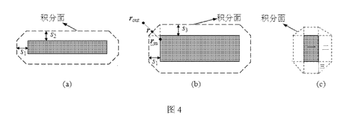
- FIG. 4 is a schematic structural view of a rectangular parallelepiped floating conductor and an integrating surface surrounding the same according to an embodiment of the present invention
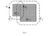
- FIG. 5 is a schematic diagram of an integration surface of a plurality of rectangular parallelepiped suspension conductors and a jump scheme thereof according to an embodiment of the present invention
- FIG. 6 is a flow chart of a method for extracting random walking capacitance parameters of a floating conductor in accordance with an embodiment of the present invention.
- the random walk capacitance extraction algorithm is a popular method in the field solver method for extracting capacitance parameters of integrated circuits. This method is different from the conventional finite difference method, finite element method and boundary element method. It does not need to solve linear equations.
- the main step in the calculation is to randomly take points in space (the process of obtaining a series of points is called For "random walking"). As shown in Figure 1, each random walk begins with a Gaussian surface around the main conductor (that is, the conductor that is to be coupled to the other conductors, such as conductor i in Figure 1), and then centered on the current point.
- the invention is based on the above problems, and proposes a method for extracting random walking capacitance parameters of a floating conductor.
- FIG. 3 is a flow chart of a method for extracting random walking capacitance parameters of a floating conductor according to an embodiment of the present invention.
- the random walk capacitance parameter extraction method for processing the floating conductor includes the following steps:
- step S1 the Green's function library and the weight vector required for random walk are loaded.
- step S2 an integral plane is constructed for each of the suspended conductor blocks, and the amount required to perform the corresponding random jump is calculated.
- the integral surface is separately constructed for each of the suspended conductor blocks, and the amount required to perform the corresponding random jump is calculated, and further includes: respectively shifting the six faces of the conductor outward by a predetermined distance Obtaining six first type faces and connecting two adjacent first type faces to obtain twelve second type faces, and connecting adjacent three second type faces to obtain 8 third type faces to obtain closed density The surface of twenty-six faces.
- the basis for randomly picking points according to the integral plane of the suspended conductor and the corresponding jump probability table is:
- ⁇ (F) is the electrostatic potential of the suspended conductor block F
- ⁇ is the integral plane
- r is the integral point on ⁇
- ⁇ (r) is the dielectric constant at the point r
- s(r) is from the r point
- the distance to the suspended conductor F along a line perpendicular to the ⁇ , r out is the point from the point r along the straight line perpendicular to the ⁇ distance s(r)
- ⁇ (r out ) is the point r out
- Electrostatic potential, P F (r) is a probability density function. Therefore, the above formula shows that the point r out is obtained by randomly taking the point r out from the point perpendicular to the line of s(r) according to the probability density function P F (r). The resulting sample point.
- the embodiment of the present invention can construct a 26-sided body surrounding the rectangular parallelepiped shaped floating conductor, the surface of which is called an integral plane, and a corresponding random jump scheme.
- Fig. 4 (a) is a top view, (b) is a front view, and (c) is a side view.
- three types of faces constituting the entire integral face are marked in the side view, and in the front view, three points r in , r and r out indicate the jump plan.
- s 1 , s 2 , s 3 are the distances of the first type of integrated surface to the suspended conductor.
- ⁇ (F) represents the electrostatic potential of the suspended conductor block F
- ⁇ is the integral plane
- r is the integral point on ⁇
- ⁇ (r) is the dielectric constant at the point r
- s(r) is from the r point
- the line perpendicular to the ⁇ reaches the distance of the suspended conductor F.
- step S2 means calculating the value of K and the function P F (r) so that the probability density function P F (r) can be randomized on the ⁇ Picking points.
- step S3 the Gaussian surface is constructed for the main conductor, and the initial value of the capacitance is set to 0 and the initial value of the random walking number is 0.
- step S4 the number of random walks is increased by 1, the initial value of the capacitance and the initial value of the random walk number are set, and a point is randomly taken on the Gaussian surface, and a transfer cube is generated centering on the surface of the transfer cube according to the Green's function library.
- the probability distribution randomly takes points, and the probability distribution is used to calculate the corresponding weights of the random points according to the weight vector.
- step S5 it is judged whether or not the current random point is not on the surface of the interconnecting conductor.
- step S6 if the current random point is on the surface of the interconnecting conductor, the capacitance value is updated by the weight and the random walking number, and it is judged whether the termination condition is satisfied, and if the termination condition is satisfied, the process ends. If the termination condition is not satisfied, the process proceeds to Step S4.
- step S7 if the current random point is not on the surface of the interconnecting conductor, it is judged whether the current random point is on the surface of the monolithic suspension conductor.
- step S8 if the current random point is on the surface of the monolithic suspension conductor, based on the integration surface of the floating conductor and the corresponding jump probability table, the random acquisition point, and update the current point, and jump to step S5;
- step S9 if the current random point is not on the surface of the monolithic suspension conductor, it is determined whether the current random point is on the surface of the suspended conductor containing the plurality of blocks;
- step S10 if the current random point is on the surface of the floating conductor containing multiple blocks, the random point is updated based on the integral plane of each rectangular block of the floating conductor and the corresponding jump probability table and the rejection sampling mode, the current point is updated, and the jump is made to Step S5;
- step S11 if the current random point is not on the surface of the floating conductor containing multiple blocks, the current random point is the centrally constructed transition cube that does not intersect any conductor, and is distributed on the transfer cube according to the probability represented by the Green's function library. Take a random point to update the current point and jump to step S5.
- the random acquisition point is performed based on the integration plane of each cuboid block of the floating conductor and the corresponding jump probability table and the manner of rejecting the sampling, and further includes: step a: according to each suspension conductor block A total of the integrated area of the integral surface is randomly selected from a floating conductor block i; step b: uniformly randomly selecting a point r on the integral surface of the floating conductor block i; step c: if the point r is included in the integral surface of the other suspended conductor block Internally, the point r is discarded, returning to step a; step d: generating a random number x uniformly distributed over the interval (0, 1); step e: if x>P F (r)/U, where U is a function P An upper limit value of F (r) is returned to step a; step f: obtaining point r is an effective sampling point on the integration surface of the floating conductor, and the falling point of the next jump is r out ,
- the steps of the random walk capacitance parameter extraction method for processing a floating conductor are as follows:
- the current random point r (x) is not on the surface of the suspended conductor k containing multiple blocks, the current random point r (x) is the largest transfer cube that does not intersect any conductor, and is represented by the Green's function library.
- the probability distribution randomly takes a point on the transition cube to update the current point, set the point to r (y) , and jump to (5).
- the embodiment of the present invention performs a capacitance extraction calculation experiment with respect to some high-density on-chip capacitor structures including complex floating conductors, and the results show that the random walk capacitance parameter extraction method for processing the floating conductor is improved by 5 times compared with the related art. Accuracy, and at a maximum accuracy of 3.7 times faster than in the related art.
- the random walk capacitance parameter extraction method for processing a floating conductor is deduced by a center-difference approximation derivation method, thereby avoiding each of the floating conductors as interconnecting conductors for capacitance extraction one by one, which can be accurately calculated quickly.
- the capacitance parameter of the integrated circuit interconnect structure including the floating conductor effectively improves the calculation accuracy, improves the robustness, and improves the computational efficiency of the algorithm.
- first and second are used for descriptive purposes only and are not to be construed as indicating or implying a relative importance or implicitly indicating the number of technical features indicated.
- features defining “first” or “second” may include at least one of the features, either explicitly or implicitly.
- the meaning of "a plurality” is at least two, such as two, three, etc., unless specifically defined otherwise.
- the terms “installation”, “connected”, “connected”, “fixed” and the like shall be understood broadly, and may be either a fixed connection or a detachable connection, unless explicitly stated and defined otherwise. , or integrated; can be mechanical or electrical connection; can be directly connected, or indirectly connected through an intermediate medium, can be the internal communication of two elements or the interaction of two elements, unless otherwise specified Limited.
- the specific meanings of the above terms in the present invention can be understood on a case-by-case basis.
- the first feature "on” or “under” the second feature may be a direct contact of the first and second features, or the first and second features may be indirectly through an intermediate medium, unless otherwise explicitly stated and defined. contact.
- the first feature "above”, “above” and “above” the second feature may be that the first feature is directly above or above the second feature, or merely that the first feature level is higher than the second feature.
- the first feature “below”, “below” and “below” the second feature may be that the first feature is directly below or obliquely below the second feature, or merely that the first feature level is less than the second feature.
Landscapes
- Engineering & Computer Science (AREA)
- Computer Hardware Design (AREA)
- Physics & Mathematics (AREA)
- Theoretical Computer Science (AREA)
- Evolutionary Computation (AREA)
- Geometry (AREA)
- General Engineering & Computer Science (AREA)
- General Physics & Mathematics (AREA)
- Management, Administration, Business Operations System, And Electronic Commerce (AREA)
- Design And Manufacture Of Integrated Circuits (AREA)
Abstract
一种处理悬浮导体的随机行走电容参数提取方法,为每个悬浮导体块构造一个含二十六个面的封闭积分面,并进行相应的随机采样,得到随机行走路径遇到悬浮导体情况时的跳转方案。该方法与拒绝采样技术结合后可以处理由多块长方体组成的复杂形状悬浮导体。将该方法用于悬浮随机行走电容提取方法中,能够较快速、准确地计算包含悬浮导体的集成电路互连线结构的电容参数,提高计算的鲁棒性和计算效率。
Description
相关申请的交叉引用
本申请要求清华大学于2017年12月18日提交的、发明名称为“处理悬浮导体的随机行走电容参数提取方法”的、中国专利申请号“201711362811.6”的优先权。
本发明涉及VLSI(Very Large Scale Integrated circuits,超大规模集成电路)物理设计技术领域,特别涉及一种处理悬浮导体的随机行走电容参数提取方法。
集成电路的设计流程中首先要提出功能描述,然后经过逻辑设计、版图设计得到描述半导体工艺尺寸、结构的版图,最后进行版图验证,即通过计算机软件模拟来验证上述设计是否满足要求,若满足要求,则进行下一步的生产制造;否则,则返回逻辑设计、版图设计进行必要的修正。在版图验证中,互连寄生参数提取是一个重要的环节。
随着集成电路制造技术的发展,电路规模不断增大、特征尺寸不断缩小,当今很多芯片已含有一千万乃至多个器件。然而,集成电路中互连线的寄生效应造成互连线对电路延时的影响已超过了器件对电路延时的影响。因此,需要对互连线的电容、电阻等参数进行准确的计算,以保证电路模拟与验证的正确有效性。为了提高计算精度,互连线之间的电容参数提取需要使用三维提取方法,即利用三维场求解器进行求解,而利用场求解器的计算往往耗时较多。
发明内容
本发明旨在至少在一定程度上解决相关技术中的技术问题之一。
为此,本发明的目的在于提出一种处理悬浮导体的随机行走电容参数提取方法,该方法可以有效提高计算的准确度,提高鲁棒性,并且提高算法的计算效率。
为达到上述目的,本发明实施例提出了一种处理悬浮导体的随机行走电容参数提取方法,包括以下步骤:步骤S1:载入随机行走所需的格林函数库和权值向量;步骤S2:对每个悬浮导体块分别构造积分面,并计算进行相应随机跳转所需量;步骤S3:对主导体构造高斯面,设置电容初值为0和随机行走次数初值为0;步骤S4:随机行走次数加1,并在所述高斯面上随机取点,以它为中心生成转移立方体,在所述转移立方体的表面按照所述格林函数库所表示的概率分布随机取点,根据所述权值向量计算概率分布随机取点相应的 权值;步骤S5:判断当前随机点是否在互连导体的表面;步骤S6:如果所述当前随机点在所述互连导体的表面,通过所述权值和所述随机行走次数更新电容值,并判断是否满足终止条件,如果满足终止条件,则结束,如果不满足终止条件,转至步骤S4;步骤S7:如果所述当前随机点不在所述互连导体的表面,判断所述当前随机点是否在单块悬浮导体表面;步骤S8:如果所述当前随机点在所述单块悬浮导体表面,基于所述悬浮导体的积分面和相应的跳转概率表进行随机采点,并更新当前点,并跳转至步骤S5;步骤S9:如果所述当前随机点不在所述单块悬浮导体表面,判断所述当前随机点是否在含多块的悬浮导体表面;步骤S10:如果所述当前随机点在含多块的悬浮导体表面,基于所述悬浮导体各个长方体块的积分面和相应跳转概率表以及拒绝采样方式进行随机采点,更新当前点,并跳转至步骤S5;步骤S11:如果所述当前随机点不在含多块的悬浮导体表面,所述当前随机点为中心构造最大的、不与任何导体相交的转移立方体,并按照所述格林函数库所表示的概率分布在转移立方体上随机取一点,以更新当前点,并跳转至步骤S5。
本发明实施例的处理悬浮导体的随机行走电容参数提取方法,可以通过基于中心差分近似求导方法推导,避免将每个悬浮导体看成互连导体逐一进行电容提取,能够较快速地准确计算包含悬浮导体的集成电路互连线结构的电容参数,有效提高计算的准确度,提高鲁棒性,并且提高算法的计算效率。
另外,根据本发明上述实施例的处理悬浮导体的随机行走电容参数提取方法还可以具有以下附加的技术特征:
进一步地,在本发明的一个实施例中,所述对每个悬浮导体块分别构造积分面,并计算进行相应随机跳转所需量,进一步包括:将所述导体的六个面分别向外平移预设距离得到六个第一类面,并连接相邻的两个所述第一类面得到十二个第二类面,且连接相邻的三个所述第二类面得到8个第三类面以得到封闭密二十六个面体的表面。
进一步地,在本发明的一个实施例中,所述基于所述悬浮导体的积分面和相应的跳转概率表进行随机采点,进一步包括:按概率密度函数P
F(r)在积分面Γ上随机采点,如得到的随机点为r,则下一步跳转的落点为r
out,其为从r点出发沿着垂直于Γ的直线向外走距离s(r)得到的点,其中,
 s(r)为从r点出发沿着垂直于Γ的直线到达悬浮导体F的距离,ε(r)为r点处的介电常数,

进一步地,在本发明的一个实施例中,所述基于所述悬浮导体的各个长方体块的积分面和相应的跳转概率表以及拒绝采样的方式进行随机采点,进一步包括:步骤a:根据各个 悬浮导体块的积分面的总面积大小随机选取一个悬浮导体块i;步骤b:在所述悬浮导体块i的积分面上均匀地随机选一个点r;步骤c:如果所述点r包含在其他悬浮导体块的积分面内部,则舍弃所述点r,返回所述步骤a;步骤d:生成一个(0,1)区间上均匀分布的随机数x;步骤e:如果x>P
F(r)/U,其中,U为函数P
F(r)的一个上限值,则返回所述步骤a;步骤f:获取所述点r为悬浮导体积分面上的有效采样点,下一步跳转的落点为r
out,其为从所述点r点出发沿着垂直于Γ的直线向外走距离s(r)得到的点。
本发明附加的方面和优点将在下面的描述中部分给出,部分将从下面的描述中变得明显,或通过本发明的实践了解到。
本发明上述的和/或附加的方面和优点从下面结合附图对实施例的描述中将变得明显和容易理解,其中:
图1为相关技术中的随机行走电容提取过程的二维示意图;
图2为相关技术中的悬浮导体的二维示意图;
图3为根据本发明实施例的处理悬浮导体的随机行走电容参数提取方法的流程图;
图4为根据本发明一个实施例的长方体悬浮导体与包围它的积分面的结构示意图;
图5为根据本发明一个实施例的多个长方体组成的悬浮导体的积分面,及其跳转方案示意图;
图6为根据本发明一个具体实施例的处理悬浮导体的随机行走电容参数提取方法的流程图。
下面详细描述本发明的实施例,所述实施例的示例在附图中示出,其中自始至终相同或类似的标号表示相同或类似的元件或具有相同或类似功能的元件。下面通过参考附图描述的实施例是示例性的,旨在用于解释本发明,而不能理解为对本发明的限制。
相关技术中,在集成电路电容参数提取的场求解器方法中,随机行走电容提取算法是一种比较流行的方法。该方法不同于常规的有限差分法、有限元法和边界元法,它无需要求解线性方程组,计算中的主要步骤是在空间中随机取点(其得到一系列点的过程被形象地称为“随机行走”)。如图1所示,每次随机行走都从围绕主导体(即要算它与其他导体间耦合电容的那个导体,如图1中的导体i)的高斯面上开始,然后以当前点为中心构造一个最大、不与导体相交的立方体(称为转移立方体),下一次取点则随机地落在转移立方体的 表面。图1中,S
(1)和S
(2)为两个转移立方体的表面(虚线框)。这个过程重复进行,直到随机取点的位置达到某个导体表面,此时结束一次随机行走。要计算主导体(如图1中的导体i)与其他所有导体之间的电容值,需要进行至少上万次的随机行走,根据每次行走对应计算出的权值求平均可以得到这些电容值。
考虑一般的数字集成电路,所有导体块和整个三维仿真空间都是长方体,并且它们的任何一条边都平行于x,y,z坐标轴中的某一个(这样的几何结构被称为曼哈顿结构)。如图1所示,随机行走算法中使用转移立方体,正是考虑到转移立方体可以与曼哈顿结构导体有较大的接触面。
在集成电路制造过程中,为了保证分层工艺的平整性、或者为了设计一些电容器结构需要在原有的互连线之间加入一些悬浮导体,即一些与电信号绝缘的导体块。它们的引入会影响互连线间的电容值,在进行三维电容提取时必须准确考虑。如图2所示,这些悬浮导体在几何上属于曼哈顿结构,但可能是由多个长方体组成的复杂形状。每个悬浮导体由于与环境绝缘,其电荷量总保持为零,处理包含悬浮导体的结构的一种方法是将每个悬浮导体看成是与互连线导体一样,算出所有导体间的耦合电容,然后计算互连线导体间电容值时需利用电容电路化简的方法消去悬浮导体对应的电路节点。
然而,由于需要把悬浮导体设置为主导体,计算它与其他所有导体间电容,增加了很多额外的计算量(尤其当悬浮导体数目很多时),计算开销很大。
本发明正是基于上述问题,而提出的一种处理悬浮导体的随机行走电容参数提取方法。
下面参照附图描述根据本发明实施例提出的处理悬浮导体的随机行走电容参数提取方法。
图3是本发明实施例的处理悬浮导体的随机行走电容参数提取方法的流程图。
如图3所示,该处理悬浮导体的随机行走电容参数提取方法包括以下步骤:
在步骤S1中,载入随机行走所需的格林函数库和权值向量。
在步骤S2中,对每个悬浮导体块分别构造积分面,并计算进行相应随机跳转所需量。
进一步地,在本发明的一个实施例中,对每个悬浮导体块分别构造积分面,并计算进行相应随机跳转所需量,进一步包括:将导体的六个面分别向外平移预设距离得到六个第一类面,并连接相邻的两个第一类面得到十二个第二类面,且连接相邻的三个第二类面得到8个第三类面以得到封闭密二十六个面体的表面。
进一步地,在本发明的一个实施例中,根据悬浮导体的积分面和相应的跳转概率表进行随机采点的依据为:

其中,φ(F)为悬浮导体块F的静电势,Γ为积分面,r为Γ上的积分点,ε(r)为r点处的介电常数,s(r)为从r点出发沿着垂直于Γ的直线到达悬浮导体F的距离,r
out为从r点出发沿着垂直于Γ的直线向外走距离s(r)得到的点,φ(r
out)为r
out点处的静电势,
 P
F(r)为概率密度函数。因此,上述公式表明,按照概率密度函数P
F(r)在Γ上随机采点r,然后由r点出发沿着垂直于Γ的直线向外走距离s(r)得到点r
out,即为得到的采样点。
P
F(r)为概率密度函数。因此,上述公式表明,按照概率密度函数P
F(r)在Γ上随机采点r,然后由r点出发沿着垂直于Γ的直线向外走距离s(r)得到点r
out,即为得到的采样点。
可以理解的是,本发明实施例可以对长方体形状的悬浮导体构造一个包围它的26面体,其表面称为积分面,以及相应的随机跳转方案。如图4所示,(a)为顶视图,(b)为正视图,(c)为侧视图。其中,在侧视图中标记了构成整个积分面的三种类型的面,在正视图中,r
in,r和r
out三个点示意了跳转方案。s
1,s
2,s
3为第一类积分面到悬浮导体的距离。具体地,它是将导体的6个面分别向外平移一定距离得到6个第一类面,然后连接相邻的两个第一类面得到12个第二类面,最后连接相邻的三个第二类面得到8个第三类面,得到封闭密26面体的表面。在组成积分面的26个面中,第一类、第二类面都是矩形,第三类面是三角形,相应的随机跳转规则遵循如下公式:

其中,
 φ(F)表示悬浮导体块F的静电势,Γ为积分面,r为Γ上的积分点,ε(r)为r点处的介电常数,s(r)为从r点出发沿着垂直于Γ的直线到达悬浮导体F的距离。在计算出K的值和函数P
F(r)之后,上述公式表明可以按概率密度函数P
F(r)在Γ上随机采点,假设得到的随机点为r,则下一步跳转的落点为r
out,它为从r点出发沿着垂直于Γ的直线向外走距离s(r)得到的点,如图4(b)所示。
φ(F)表示悬浮导体块F的静电势,Γ为积分面,r为Γ上的积分点,ε(r)为r点处的介电常数,s(r)为从r点出发沿着垂直于Γ的直线到达悬浮导体F的距离。在计算出K的值和函数P
F(r)之后,上述公式表明可以按概率密度函数P
F(r)在Γ上随机采点,假设得到的随机点为r,则下一步跳转的落点为r
out,它为从r点出发沿着垂直于Γ的直线向外走距离s(r)得到的点,如图4(b)所示。
另外,在步骤S2中的“计算进行相应随机跳转所需的一些量”指的是计算K的值和函数P
F(r),使得可以依照概率密度函数P
F(r)在Γ上随机采点。
在步骤S3中,对主导体构造高斯面,设置电容初值为0和随机行走次数初值为0。
在步骤S4中随机行走次数加1,设置电容初值和随机行走次数初值,并在高斯面上随机取点,以它为中心生成转移立方体,在转移立方体的表面按照格林函数库所表示的概率分布随机取点,根据权值向量计算概率分布随机取点相应的权值。
在步骤S5中,判断当前随机点是否不在互连导体的表面。
在步骤S6中,如果当前随机点在互连导体的表面,通过权值和随机行走次数更新电容值,并判断是否满足终止条件,如果满足终止条件,则结束,如果不满足终止条件,转至步骤S4。
在步骤S7中,如果当前随机点不在互连导体的表面,判断当前随机点是否在单块悬浮导体表面。
在步骤S8中,如果当前随机点在单块悬浮导体表面,基于悬浮导体的积分面和相应的跳转概率表进行随机采点,并更新当前点,并跳转至步骤S5;
在步骤S9中,如果当前随机点不在单块悬浮导体表面,判断当前随机点是否在含多块的悬浮导体表面;
在步骤S10中,如果当前随机点在含多块的悬浮导体表面,基于悬浮导体各个长方体块的积分面和相应跳转概率表以及拒绝采样方式进行随机采点,更新当前点,并跳转至步骤S5;以及
在步骤S11中,如果当前随机点不在含多块的悬浮导体表面,当前随机点为中心构造最大的、不与任何导体相交的转移立方体,并按照格林函数库所表示的概率分布在转移立方体上随机取一点,以更新当前点,并跳转至步骤S5。
进一步地,在本发明的一个实施例中,基于悬浮导体的各个长方体块的积分面和相应的跳转概率表以及拒绝采样的方式进行随机采点,进一步包括:步骤a:根据各个悬浮导体块的积分面的总面积大小随机选取一个悬浮导体块i;步骤b:在悬浮导体块i的积分面上均匀地随机选一个点r;步骤c:如果点r包含在其他悬浮导体块的积分面内部,则舍弃点r,返回步骤a;步骤d:生成一个(0,1)区间上均匀分布的随机数x;步骤e:如果x>P
F(r)/U,其中,U为函数P
F(r)的一个上限值,则返回步骤a;步骤f:获取点r为悬浮导体积分面上的有效采样点,下一步跳转的落点为r
out,其为从点r点出发沿着垂直于Γ的直线向外走距离s(r)得到的点。
可以理解的是,本发明实施例需考虑由多个长方体块组成的较复杂的悬浮导体,其中,每个长方体悬浮导体块的跳转方案已经是可行的。具体地,
a)首先根据各个悬浮导体块的积分面的总面积大小,随机选取一个悬浮导体块i;
b)在悬浮导体块i的积分面上均匀地随机选一个点r;
c)如果点r包含在其他悬浮导体块的积分面内部,如图5的点r
2,则舍弃该点,返回步骤a);
d)生成一个(0,1)区间上均匀分布的随机数x;
e)如果x>P
F(r)/U,其中,U为函数P
F(r)的一个上限值,则返回步骤a);
f)得到r为悬浮导体积分面上的有效采样点,下一步跳转的落点为r
out,它为从r点出发沿着垂直于Γ的直线向外走距离s(r)得到的点,如图4(b)所示。
举例而言,如图6所示,本发明一个具体实施例的处理悬浮导体的随机行走电容参数提取方法的步骤如下:
(1)载入随机行走所需的格林函数库和权值向量。
(2)对每个悬浮导体块,构造它的积分面,并计算进行相应随机跳转所需的一些量。
(3)对主导体i构造高斯面,并设置电容初值:
 设置随机行走次数初值npath:=0;
(4)随机行走次数加1,在主导体i的高斯面上随机取点r,以为中心生成转移立方体,在该转移立方体表面按照格林函数库所表示的概率分布随机取点r
(1),在载入的权值向量的帮助下计算r
(1)相应的权值ω。
(5)判断当前随机点r
(x)是否在互连导体的表面
(6)如果当前随机点r
(x)在互连导体的表面,通过权值和随机行走次数更新电容值,并判断是否满足终止条件,如果满足终止条件,即r
(x):=r
(y)时,则结束,如果不满足终止条件,转至(4);
(7)如果当前随机点r
(x)不在互连导体的表面,判断当前随机点r
(x)是否在单块悬浮导体k表面;
(8)如果当前随机点r
(x)在单块悬浮导体k表面,基于悬浮导体k的积分面和相应的跳转概率表进行随机采点,并更新当前点,将该点设为r
(y),并跳转至(5);
(9)如果当前随机点r
(x)不在单块悬浮导体k表面,判断当前随机点r
(x)是否在含多块的悬浮导体k表面;
(10)如果当前随机点r
(x)在含多块的悬浮导体k表面,基于悬浮导体k各个长方体块的积分面和相应跳转概率表以及拒绝采样方式进行随机采点,更新当前点,将得到的点设为r
(y),并跳转至(5);以及
(11)如果当前随机点r
(x)不在含多块的悬浮导体k表面,当前随机点r
(x)为中心构造最 大的、不与任何导体相交的转移立方体,并按照格林函数库所表示的概率分布在转移立方体上随机取一点,以更新当前点,将该点设为r
(y),并跳转至(5)。
可以理解的是,本发明实施例相对于一些包含复杂悬浮导体的高密度片上电容器结构进行电容提取计算实验,结果表明,处理悬浮导体的随机行走电容参数提取方法相比于相关技术提高了5倍的准确度,并且在相对的准确度要求的情况下最多比相关技术中快3.7倍。
根据本发明实施例提出的处理悬浮导体的随机行走电容参数提取方法,通过基于中心差分近似求导方法推导,避免将每个悬浮导体看成互连导体逐一进行电容提取,能够较快速地准确计算包含悬浮导体的集成电路互连线结构的电容参数,有效提高计算的准确度,提高鲁棒性,并且提高算法的计算效率。
在本发明的描述中,需要理解的是,术语“中心”、“纵向”、“横向”、“长度”、“宽度”、“厚度”、“上”、“下”、“前”、“后”、“左”、“右”、“竖直”、“水平”、“顶”、“底”“内”、“外”、“顺时针”、“逆时针”、“轴向”、“径向”、“周向”等指示的方位或位置关系为基于附图所示的方位或位置关系,仅是为了便于描述本发明和简化描述,而不是指示或暗示所指的装置或元件必须具有特定的方位、以特定的方位构造和操作,因此不能理解为对本发明的限制。
此外,术语“第一”、“第二”仅用于描述目的,而不能理解为指示或暗示相对重要性或者隐含指明所指示的技术特征的数量。由此,限定有“第一”、“第二”的特征可以明示或者隐含地包括至少一个该特征。在本发明的描述中,“多个”的含义是至少两个,例如两个,三个等,除非另有明确具体的限定。
在本发明中,除非另有明确的规定和限定,术语“安装”、“相连”、“连接”、“固定”等术语应做广义理解,例如,可以是固定连接,也可以是可拆卸连接,或成一体;可以是机械连接,也可以是电连接;可以是直接相连,也可以通过中间媒介间接相连,可以是两个元件内部的连通或两个元件的相互作用关系,除非另有明确的限定。对于本领域的普通技术人员而言,可以根据具体情况理解上述术语在本发明中的具体含义。
在本发明中,除非另有明确的规定和限定,第一特征在第二特征“上”或“下”可以是第一和第二特征直接接触,或第一和第二特征通过中间媒介间接接触。而且,第一特征在第二特征“之上”、“上方”和“上面”可是第一特征在第二特征正上方或斜上方,或仅仅表示第一特征水平高度高于第二特征。第一特征在第二特征“之下”、“下方”和“下面”可以是第一特征在第二特征正下方或斜下方,或仅仅表示第一特征水平高度小于第二特征。
在本说明书的描述中,参考术语“一个实施例”、“一些实施例”、“示例”、“具体示例”、或“一些示例”等的描述意指结合该实施例或示例描述的具体特征、结构、材料或者特点包 含于本发明的至少一个实施例或示例中。在本说明书中,对上述术语的示意性表述不必须针对的是相同的实施例或示例。而且,描述的具体特征、结构、材料或者特点可以在任一个或多个实施例或示例中以合适的方式结合。此外,在不相互矛盾的情况下,本领域的技术人员可以将本说明书中描述的不同实施例或示例以及不同实施例或示例的特征进行结合和组合。
尽管上面已经示出和描述了本发明的实施例,可以理解的是,上述实施例是示例性的,不能理解为对本发明的限制,本领域的普通技术人员在本发明的范围内可以对上述实施例进行变化、修改、替换和变型。
Claims (4)
- 一种处理悬浮导体的随机行走电容参数提取方法,其特征在于,包括以下步骤:步骤S1:载入随机行走所需的格林函数库和权值向量;步骤S2:对每个悬浮导体块分别构造积分面,并计算进行相应随机跳转所需量;步骤S3:对主导体构造高斯面,设置电容初值为0和随机行走次数初值为0;步骤S4:随机行走次数加1,并在所述高斯面上随机取点,以它为中心生成转移立方体,在所述转移立方体的表面按照所述格林函数库所表示的概率分布随机取点,根据所述权值向量计算随机取点相应的权值;步骤S5:判断当前随机点是否在互连导体的表面;步骤S6:如果所述当前随机点在所述互连导体的表面,通过所述权值和所述随机行走次数更新电容值,并判断是否满足终止条件,如果满足终止条件,则结束,如果不满足终止条件,转至步骤S4;步骤S7:如果所述当前随机点不在所述互连导体的表面,判断所述当前随机点是否在单块悬浮导体表面;步骤S8:如果所述当前随机点在所述单块悬浮导体表面,基于所述悬浮导体的积分面和相应的跳转概率表进行随机采点,并更新当前点,并跳转至步骤S5;步骤S9:如果所述当前随机点不在所述单块悬浮导体表面,判断所述当前随机点是否在含多块的悬浮导体表面;步骤S10:如果所述当前随机点在含多块的悬浮导体表面,基于所述悬浮导体各个长方体块的积分面和相应跳转概率表以及拒绝采样方式进行随机采点,更新当前点,并跳转至步骤S5;以及步骤S11:如果所述当前随机点不在含多块的悬浮导体表面,所述当前随机点为中心构造最大的、不与任何导体相交的转移立方体,并按照所述格林函数库所表示的概率分布在转移立方体上随机取一点,以更新当前点,并跳转至步骤S5。
- 根据权利要求1所述的处理悬浮导体的随机行走电容参数提取方法,其特征在于,所述对每个悬浮导体块分别构造积分面,并计算进行相应随机跳转所需量,进一步包括:将所述导体的六个面分别向外平移预设距离得到六个第一类面,并连接相邻的两个所述第一类面得到十二个第二类面,且连接相邻的三个所述第二类面得到8个第三类面以得到封闭二十六面体的表面。
- 根据权利要求1或2所述的处理悬浮导体的随机行走电容参数提取方法,其特征在于,所述基于所述悬浮导体的积分面和相应的跳转概率表进行随机采点,进一步包括:按概率密度函数P F(r)在积分面Γ上随机采点,如得到的随机点为r,则下一步跳转的落点为r out,其为从r点出发沿着垂直于Γ的直线向外走距离s(r)得到的点;其中,s(r)为从r点出发沿着垂直于Γ的直线到达悬浮导体F的距离,ε(r)为r点处的介电常数,


- 根据权利要求3所述的处理悬浮导体的随机行走电容参数提取方法,其特征在于,所述基于所述悬浮导体的各个长方体块的积分面和相应的跳转概率表以及拒绝采样的方式进行随机采点,进一步包括:步骤a:根据各个悬浮导体块的积分面的总面积大小随机选取一个悬浮导体块i;步骤b:在所述悬浮导体块i的积分面上均匀地随机选一个点r;步骤c:如果所述点r包含在其他悬浮导体块的积分面内部,则舍弃所述点r,返回所述步骤a;步骤d:生成一个(0,1)区间上均匀分布的随机数x;步骤e:如果x>P F(r)/U,其中,U为函数P F(r)的一个上限值,则返回所述步骤a;步骤f:获取所述点r为悬浮导体积分面上的有效采样点,下一步跳转的落点为r out,其为从所述点r点出发沿着垂直于Γ的直线向外走距离s(r)得到的点。
Applications Claiming Priority (2)
| Application Number | Priority Date | Filing Date | Title |
|---|---|---|---|
| CN201711362811.6A CN107844674B (zh) | 2017-12-18 | 2017-12-18 | 处理悬浮导体的随机行走电容参数提取方法 |
| CN201711362811.6 | 2017-12-18 |
Publications (1)
| Publication Number | Publication Date |
|---|---|
| WO2019119759A1 true WO2019119759A1 (zh) | 2019-06-27 |
Family
ID=61664196
Family Applications (1)
| Application Number | Title | Priority Date | Filing Date |
|---|---|---|---|
| PCT/CN2018/092482 Ceased WO2019119759A1 (zh) | 2017-12-18 | 2018-06-22 | 处理悬浮导体的随机行走电容参数提取方法 |
Country Status (2)
| Country | Link |
|---|---|
| CN (1) | CN107844674B (zh) |
| WO (1) | WO2019119759A1 (zh) |
Cited By (1)
| Publication number | Priority date | Publication date | Assignee | Title |
|---|---|---|---|---|
| CN115906752A (zh) * | 2022-10-24 | 2023-04-04 | 清华大学 | 非分层介质处理方法及装置、电子设备和存储介质 |
Families Citing this family (5)
| Publication number | Priority date | Publication date | Assignee | Title |
|---|---|---|---|---|
| CN107844674B (zh) * | 2017-12-18 | 2019-06-28 | 清华大学 | 处理悬浮导体的随机行走电容参数提取方法 |
| CN114036892A (zh) * | 2022-01-08 | 2022-02-11 | 青岛展诚科技有限公司 | 随机行走在电容抽取中单细粒度的并行处理方法和系统 |
| CN114707463A (zh) * | 2022-04-12 | 2022-07-05 | 杭州行芯科技有限公司 | 基于随机行走的寄生电容提取方法、装置和电子装置 |
| WO2023193812A1 (zh) * | 2022-04-08 | 2023-10-12 | 杭州行芯科技有限公司 | 寄生电容提取方法、电子装置和存储介质 |
| CN117494646B (zh) * | 2023-12-29 | 2024-05-28 | 杭州行芯科技有限公司 | 电容获取方法、电子设备及存储介质 |
Citations (6)
| Publication number | Priority date | Publication date | Assignee | Title |
|---|---|---|---|---|
| CN102651047A (zh) * | 2012-04-11 | 2012-08-29 | 清华大学 | 集成电路设计中基于随机行走的电容参数提取计算方法 |
| CN105335567A (zh) * | 2015-11-05 | 2016-02-17 | 清华大学 | 适应非曼哈顿形体的随机行走电容参数提取方法及系统 |
| US20160180007A1 (en) * | 2014-12-22 | 2016-06-23 | Synopsys, Inc. | Optimization Of Parasitic Capacitance Extraction Using Statistical Variance Reduction Technique |
| CN105930572A (zh) * | 2016-04-15 | 2016-09-07 | 清华大学 | 一种面向触摸屏电容仿真的多介质预刻画方法 |
| US20160342729A1 (en) * | 2015-05-22 | 2016-11-24 | Helic, Inc. | Method of extracting capacitances of arbitrarily oriented 3d interconnects |
| CN107844674A (zh) * | 2017-12-18 | 2018-03-27 | 清华大学 | 处理悬浮导体的随机行走电容参数提取方法 |
Family Cites Families (2)
| Publication number | Priority date | Publication date | Assignee | Title |
|---|---|---|---|---|
| US8122419B2 (en) * | 2008-11-09 | 2012-02-21 | International Business Machines Corporation | System and method for three-dimensional variational capacitance calculation |
| CN104008255B (zh) * | 2014-06-13 | 2017-01-18 | 清华大学 | 面向集成电路电容提取的多介质随机行走方法及系统 |
-
2017
- 2017-12-18 CN CN201711362811.6A patent/CN107844674B/zh active Active
-
2018
- 2018-06-22 WO PCT/CN2018/092482 patent/WO2019119759A1/zh not_active Ceased
Patent Citations (6)
| Publication number | Priority date | Publication date | Assignee | Title |
|---|---|---|---|---|
| CN102651047A (zh) * | 2012-04-11 | 2012-08-29 | 清华大学 | 集成电路设计中基于随机行走的电容参数提取计算方法 |
| US20160180007A1 (en) * | 2014-12-22 | 2016-06-23 | Synopsys, Inc. | Optimization Of Parasitic Capacitance Extraction Using Statistical Variance Reduction Technique |
| US20160342729A1 (en) * | 2015-05-22 | 2016-11-24 | Helic, Inc. | Method of extracting capacitances of arbitrarily oriented 3d interconnects |
| CN105335567A (zh) * | 2015-11-05 | 2016-02-17 | 清华大学 | 适应非曼哈顿形体的随机行走电容参数提取方法及系统 |
| CN105930572A (zh) * | 2016-04-15 | 2016-09-07 | 清华大学 | 一种面向触摸屏电容仿真的多介质预刻画方法 |
| CN107844674A (zh) * | 2017-12-18 | 2018-03-27 | 清华大学 | 处理悬浮导体的随机行走电容参数提取方法 |
Cited By (1)
| Publication number | Priority date | Publication date | Assignee | Title |
|---|---|---|---|---|
| CN115906752A (zh) * | 2022-10-24 | 2023-04-04 | 清华大学 | 非分层介质处理方法及装置、电子设备和存储介质 |
Also Published As
| Publication number | Publication date |
|---|---|
| CN107844674B (zh) | 2019-06-28 |
| CN107844674A (zh) | 2018-03-27 |
Similar Documents
| Publication | Publication Date | Title |
|---|---|---|
| CN107844674B (zh) | 处理悬浮导体的随机行走电容参数提取方法 | |
| US10013522B2 (en) | Method of extracting capacitances of arbitrarily oriented 3D interconnects | |
| CN104008255B (zh) | 面向集成电路电容提取的多介质随机行走方法及系统 | |
| CN103198177B (zh) | 基于gpu的集成电路电容参数提取系统及方法 | |
| CN102651047B (zh) | 集成电路设计中基于随机行走的电容参数提取计算方法 | |
| US6963122B1 (en) | Capacitor structure and automated design flow for incorporating same | |
| CN114662445B (zh) | 用于寄生电容提取的随机行走方法、装置和电子装置 | |
| CN103473402B (zh) | 面向集成电路互连电容参数提取的空间管理数据生成方法 | |
| US8954308B2 (en) | Modeling of multi-layered power/ground planes using triangle elements | |
| CN114373635B (zh) | 量子比特的电容、量子比特及其构建方法 | |
| CN103793557B (zh) | 面向集成电路互连电容提取的线网高斯面采样方法及系统 | |
| US10274533B1 (en) | Pre-computation system and method for transition domain characterization within a floating random walk based multi-dielectric capacitance extraction methodology | |
| CN114036892A (zh) | 随机行走在电容抽取中单细粒度的并行处理方法和系统 | |
| Yu et al. | Floating random walk-based capacitance simulation considering general floating metals | |
| Kasai et al. | Neural network-based 3D IC interconnect capacitance extraction | |
| CN102024083B (zh) | 一种提取含有冗余金属的互连结构的电容的方法 | |
| CN103745069A (zh) | 三维集成电路中tsv的信号传输及功耗模型的建立方法 | |
| Batterywala et al. | A statistical method for fast and accurate capacitance extraction in the presence of floating dummy fills | |
| CN105095567B (zh) | 电容参数提取方法 | |
| CN112800710A (zh) | 面向集成电路互连电容提取的多介质格林函数预刻画方法 | |
| US8413098B2 (en) | T-connections, methodology for designing T-connections, and compact modeling of T-connections | |
| CN114707463A (zh) | 基于随机行走的寄生电容提取方法、装置和电子装置 | |
| CN105930572B (zh) | 一种面向触摸屏电容仿真的多介质预刻画方法 | |
| CN116502595A (zh) | 基于随机行走的电容提取方法及装置、设备、介质 | |
| Ren et al. | 3-D capacitance extraction of IC interconnects using field solvers and homogenization technique |
Legal Events
| Date | Code | Title | Description |
|---|---|---|---|
| 121 | Ep: the epo has been informed by wipo that ep was designated in this application |
Ref document number: 18891728 Country of ref document: EP Kind code of ref document: A1 |
|
| NENP | Non-entry into the national phase |
Ref country code: DE |
|
| 122 | Ep: pct application non-entry in european phase |
Ref document number: 18891728 Country of ref document: EP Kind code of ref document: A1 |