WO2019097699A1 - Power conversion device - Google Patents
Power conversion device Download PDFInfo
- Publication number
- WO2019097699A1 WO2019097699A1 PCT/JP2017/041566 JP2017041566W WO2019097699A1 WO 2019097699 A1 WO2019097699 A1 WO 2019097699A1 JP 2017041566 W JP2017041566 W JP 2017041566W WO 2019097699 A1 WO2019097699 A1 WO 2019097699A1
- Authority
- WO
- WIPO (PCT)
- Prior art keywords
- capacitor
- power conversion
- capacitance
- power
- main circuit
- Prior art date
Links
Images


Classifications
-
- H—ELECTRICITY
- H02—GENERATION; CONVERSION OR DISTRIBUTION OF ELECTRIC POWER
- H02M—APPARATUS FOR CONVERSION BETWEEN AC AND AC, BETWEEN AC AND DC, OR BETWEEN DC AND DC, AND FOR USE WITH MAINS OR SIMILAR POWER SUPPLY SYSTEMS; CONVERSION OF DC OR AC INPUT POWER INTO SURGE OUTPUT POWER; CONTROL OR REGULATION THEREOF
- H02M7/00—Conversion of ac power input into dc power output; Conversion of dc power input into ac power output
- H02M7/02—Conversion of ac power input into dc power output without possibility of reversal
- H02M7/04—Conversion of ac power input into dc power output without possibility of reversal by static converters
-
- H—ELECTRICITY
- H02—GENERATION; CONVERSION OR DISTRIBUTION OF ELECTRIC POWER
- H02M—APPARATUS FOR CONVERSION BETWEEN AC AND AC, BETWEEN AC AND DC, OR BETWEEN DC AND DC, AND FOR USE WITH MAINS OR SIMILAR POWER SUPPLY SYSTEMS; CONVERSION OF DC OR AC INPUT POWER INTO SURGE OUTPUT POWER; CONTROL OR REGULATION THEREOF
- H02M3/00—Conversion of dc power input into dc power output
- H02M3/02—Conversion of dc power input into dc power output without intermediate conversion into ac
- H02M3/04—Conversion of dc power input into dc power output without intermediate conversion into ac by static converters
- H02M3/10—Conversion of dc power input into dc power output without intermediate conversion into ac by static converters using discharge tubes with control electrode or semiconductor devices with control electrode
- H02M3/145—Conversion of dc power input into dc power output without intermediate conversion into ac by static converters using discharge tubes with control electrode or semiconductor devices with control electrode using devices of a triode or transistor type requiring continuous application of a control signal
- H02M3/155—Conversion of dc power input into dc power output without intermediate conversion into ac by static converters using discharge tubes with control electrode or semiconductor devices with control electrode using devices of a triode or transistor type requiring continuous application of a control signal using semiconductor devices only
-
- H—ELECTRICITY
- H02—GENERATION; CONVERSION OR DISTRIBUTION OF ELECTRIC POWER
- H02M—APPARATUS FOR CONVERSION BETWEEN AC AND AC, BETWEEN AC AND DC, OR BETWEEN DC AND DC, AND FOR USE WITH MAINS OR SIMILAR POWER SUPPLY SYSTEMS; CONVERSION OF DC OR AC INPUT POWER INTO SURGE OUTPUT POWER; CONTROL OR REGULATION THEREOF
- H02M7/00—Conversion of ac power input into dc power output; Conversion of dc power input into ac power output
- H02M7/42—Conversion of dc power input into ac power output without possibility of reversal
- H02M7/44—Conversion of dc power input into ac power output without possibility of reversal by static converters
- H02M7/48—Conversion of dc power input into ac power output without possibility of reversal by static converters using discharge tubes with control electrode or semiconductor devices with control electrode
Definitions
- the present invention relates to a power converter including a smoothing capacitor.
- IGBTs insulated gate bipolar transistors
- the capacitance of the smoothing capacitor is increased by connecting a plurality of capacitors in parallel to configure the smoothing capacitor. Also, by connecting a plurality of converter cells provided with a small-capacity capacitor for smoothing in parallel to form a large-capacity power converter, the capacitors are connected in parallel to increase the capacitance of the smoothing capacitor of the power converter. Do.
- LC resonance may occur due to the capacitance of the capacitors and the wiring inductance between the capacitors and the internal inductance of the capacitors.
- the resonant frequency matches the switching frequency of the switching element and its integral multiple, the impedance of the resonant path decreases and the capacitor current increases significantly. As the capacitor current increases, the power loss of the capacitor increases and the life of the capacitor decreases.
- a capacitor having a positive temperature characteristic in which capacitance increases with temperature rise and a capacitor having a negative temperature characteristic in which capacitance decreases with temperature rise are connected in parallel. This offsets the change in capacitance with changes in temperature.
- the present invention can provide a power conversion device capable of suppressing a variation in capacitance of a capacitor due to temperature and suppressing current imbalance in the capacitor.
- a power conversion device comprises a plurality of capacitors connected to the input side or the output side of a power conversion circuit and absorbing harmonic current, and a plurality of capacitors Includes a first capacitor and a second capacitor connected in parallel to each other, and the first capacitor and the second capacitor have internal impedances having capacitances, equivalent series resistances and inductances,
- the first capacitor has positive temperature characteristics in terms of capacitance
- the second capacitor has negative temperature characteristics in terms of capacitance.
- the second capacitor has a static characteristic against temperature variations of the first capacitor and the second capacitor. An increase in the imbalance of the harmonic current in the first capacitor and the second capacitor due to the change in capacitance is either of the components of the internal impedance Mitigated by the change.
- a power conversion device includes a power conversion main circuit and a plurality of capacitors connected to the input side or the output side of the power conversion circuit and absorbing harmonic current.
- the plurality of capacitors include a first capacitor and a second capacitor connected in parallel with one another, the first capacitor having a positive temperature characteristic of capacitance, and the second capacitor being static.
- the capacitance has a negative temperature characteristic
- the first capacitor has a negative frequency characteristic of the capacitance
- the second capacitor has a positive frequency characteristic of the capacitance.
- the power conversion main circuit, and a plurality of capacitors connected to the input side or the output side of the power conversion circuit and absorbing harmonic current which are a plurality of capacitors
- a plurality of capacitors Includes a first capacitor and a second capacitor connected in parallel with one another, the first capacitor having positive temperature characteristics in capacitance, and the second capacitor having negative temperature characteristics in capacitance
- the first capacitor has negative temperature characteristics in the equivalent series resistance
- the second capacitor has positive temperature characteristics in the equivalent series resistance.
- the present invention it is possible to suppress the variation due to the temperature of the capacitance of the capacitor connected to the input side or the output side of the power conversion circuit, and to suppress the current unbalance in the smoothing capacitor.
- the effect is clarified by the following description of the embodiment.
- the frequency characteristic of LC resonance is shown.
- the temperature characteristic of the capacitance of each smoothing capacitor is shown.
- the frequency characteristic of the capacitance of each smoothing capacitor is shown.
- the power converter device which is a modification of Example 1 is shown.
- the power converter which is other modification of Example 1 is shown.
- the temperature characteristic of the equivalent series resistance of each smoothing capacitor is shown.
- the power converter device which is a modification of Example 2 is shown.
- the power converter which is other modification of Example 2 is shown.
- the carrier and modulation wave which are used for PWM control of a power converter in Example 3 are shown.
- the equivalent circuit of a capacitor is shown.
- An example of the frequency characteristic of the impedance of a capacitor is shown.
- the power converter which is a modification of Example 4 is shown.
- the relationship between the element life of the capacitor and the operating temperature is shown.
- the power converter which is a modification of Example 5 is shown.
- the power converter which is other modification of Example 5 is shown.
- a power conversion device includes a power conversion main circuit including a semiconductor element for power conversion, and a plurality of power conversion circuits connected to the input side or the output side of the power conversion circuit to absorb harmonic currents.
- a capacitor eg, a smoothing capacitor or a filter capacitor
- the plurality of capacitors include a first capacitor and a second capacitor connected in parallel with one another, and these capacitors have internal impedances that are components of capacitance, equivalent series resistance and inductance.
- the equivalent circuit of the first capacitor and the second capacitor is, like the known capacitor, a series connection circuit of these components.
- the first capacitor has positive temperature characteristics in capacitance
- the second capacitor has negative temperature characteristics in capacitance.
- the temperature change of the total capacitance of the parallel connection of the first capacitor and the second capacitor is suppressed.
- the ability to absorb harmonic currents is maintained without variation.
- the capacitance value of each capacitor is different, there is a possibility that the magnitude of the harmonic current absorbed by the first capacitor and the second capacitor may vary.
- the increase in the imbalance of the harmonic current in the first capacitor and the second capacitor due to the fluctuation of the capacitance with the temperature fluctuation of the first capacitor and the second capacitor is It is mitigated by the change of the impedance component, that is, the capacitance and either the equivalent series resistance or the inductance.
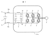
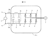
- FIG. 1 is a circuit diagram showing the configuration of a power conversion device according to a first embodiment of the present invention.
- the DC power supply 1 is connected between the input terminals 1a and 1b, and the DC side of the power conversion main circuit configured by the semiconductor switching element 2 is connected to the DC power supply 1. It is connected via a plurality of smoothing capacitors 41 and 42. Further, the AC side of the power conversion main circuit, that is, the output of the power conversion circuit is connected to the load 6.
- the smoothing capacitor 41 has a positive temperature characteristic of electrostatic capacitance.
- the smoothing capacitor 42 connected in parallel to the smoothing capacitor 41 has a negative temperature characteristic of electrostatic capacitance. Therefore, in the present embodiment, the positive and negative values of the amount of change in capacitance of the smoothing capacitor 41 and the smoothing capacitor 42 with temperature change are opposite to each other. As a result, the amounts of change in the capacitances of the smoothing capacitor 41 and the smoothing capacitor 42 cancel each other out, and the temperature fluctuation of the value of the total capacitance of the smoothing capacitor group 4a is suppressed. For example, if the absolute value of each variation is made substantially the same, the total capacitance of the smoothing capacitor group 4a is kept constant even if the temperature fluctuates.
- the plurality of smoothing capacitors 41 and 42 are connected in parallel with each other via the wiring inductance 5 to form a smoothing capacitor group 4 a.
- the smoothing capacitors 41 and 42 constituting the smoothing capacitor group 4a are arranged adjacent to each other.
- the smoothing capacitor group 4a is connected to the DC power supply 1 through the wiring inductance 10a and the input terminals 1a and 1b. Therefore, in the first embodiment, the smoothing capacitor 41 is connected in parallel to the DC power supply through the wiring inductance 10 a among the wiring inductances 5 and 10 a, and parallel to the DC side of the power conversion main circuit through the wiring inductance 5. Connected to Further, the smoothing capacitor 42 is connected in parallel to the DC power supply through the wiring inductance 5 and 10a among the wiring inductances 5 and 10a, and in parallel to the DC side of the power conversion main circuit without the wiring inductance 5 and 10a.
- the value of the wiring inductance 5 is sufficiently smaller than the value of the wiring inductance 10a. That is, the wiring length between the smoothing capacitors 41 and 42 is sufficiently shorter than the wiring length between the smoothing capacitor group 4 a and the DC power supply 1.
- the power conversion main circuit is a three-phase inverter provided with a three-phase full bridge circuit formed of the semiconductor switching element 2, and the load 6 is a three-phase AC load such as a three-phase AC motor.
- the semiconductor switching element 2 an IGBT (Insulated Gate Bipolar Transistor), a MOSFET (Metal Oxide Semiconductor Field Effect Transistor), or the like is applied (in FIG. 1, the IGBT is described).
- one arm of the three-phase full bridge circuit is formed of one semiconductor switching element 2.
- the present invention is not limited to this. Even if a plurality of semiconductor switching elements are connected in series and parallel, good.
- the power conversion device 101a turns DC power supplied from the DC power supply 1 into AC power by turning on / off the semiconductor switching element 2 constituting the power conversion main circuit by switching control such as PWM control (PWM: Pulse Width Modulation). It converts to electric power and outputs this AC power to the load 6. That is, the power conversion device 101a is an inverse converter (inverter). At this time, ripple current flows through the smoothing capacitor group 4, but the magnitude of the ripple current is determined by the capacitance of the smoothing capacitor 41, the capacitance of the smoothing capacitor 42, and the wiring inductance between the smoothing capacitor 41 and the smoothing capacitor 42. 5 depends on LC resonance.
- PWM Pulse Width Modulation
- FIG. 2 shows frequency characteristics of LC resonance.
- the switching frequency of the semiconductor switching element 2 matches the resonant frequency 118
- a large ripple current flows in the smoothing capacitor group 4a.
- the capacitor temperature rises.
- the smoothing capacitor 41 having a positive temperature characteristic in electrostatic capacitance the electrostatic capacitance is increased.
- the smoothing capacitor 42 having a negative temperature characteristic in electrostatic capacitance reduces the electrostatic capacitance.
- the capacitor current i is represented by the equation (1), where C is a capacitance and V is a capacitor voltage.
- dV / dt represents the time rate of change of the capacitor voltage.
- the characteristics of the smoothing capacitor 41 and the smoothing capacitor 42 are made different as described below.
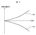
- FIG. 3 shows temperature characteristics of the capacitances of the smoothing capacitor 41 and the smoothing capacitor 42.
- the vertical axis represents the change in capacitance, and the horizontal axis represents temperature.
- the capacitance of the smoothing capacitor 41 has a positive temperature characteristic 102b, and the capacitance of the smoothing capacitor 42 has a negative temperature characteristic 102a.
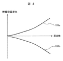
- FIG. 4 shows frequency characteristics of the capacitances of the smoothing capacitor 41 and the smoothing capacitor 42.
- the vertical axis indicates the change in capacitance, and the horizontal axis indicates the frequency.
- the capacitance of the smoothing capacitor 41 has a negative frequency characteristic 103b, and the capacitance of the smoothing capacitor 42 shows a positive frequency characteristic 103a.
- the capacitance of the smoothing capacitor 41 has positive temperature characteristics and negative frequency characteristics
- the increase in capacitance due to temperature rise is due to the negative frequency characteristics at high frequencies close to the resonance frequency. It is offset by the decrease in capacitance. For this reason, the increase in the current flowing to the smoothing capacitor 41 is suppressed.
- the capacitance of the smoothing capacitor 42 has negative temperature characteristics and a positive frequency
- the decrease in the capacitance due to temperature rise is caused by the positive frequency characteristics at high frequencies close to the resonance frequency. Offset by an increase in For this reason, a reduction in the current flowing to the smoothing capacitor 41 is suppressed. For this reason, the increase in current unbalance between the smoothing capacitor 41 and the smoothing capacitor 42 is prevented.
- film capacitors having different dielectric film materials are applied as the smoothing capacitors having different temperature characteristics and frequency characteristics of capacitance.
- the dielectric film material is appropriately selected from polypropylene, polyethylene terephthalate, polyphenylene sulfide, polyethylene, polyester and the like.
- a film capacitor using polypropylene as a dielectric film material is applied as the smoothing capacitor 41
- a film capacitor using polyethylene terephthalate as a dielectric film material is applied as the smoothing capacitor 42.
- An electrolytic capacitor, a ceramic capacitor, or the like may be applied as long as it is a capacitor that can obtain temperature characteristics and frequency characteristics of positive and negative electrostatic capacitances as well as the film capacitors.
- a film capacitor has a relatively high withstand voltage and low loss. Such a feature is suitable for a power converter.
- film capacitors have temperature characteristics of capacitance. Therefore, the first embodiment is particularly suitable when a film capacitor is applied (the same applies to each embodiment and each modification described later).
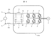
- FIG. 5 shows a power converter according to a modification of the first embodiment.
- the value of the inductance of the wiring inductance 5 is sufficiently smaller than the value of the wiring inductance 10b (corresponding to the wiring inductance 10a in FIG. 1). As well).
- the power conversion device 101b (FIG. 5) has the same circuit configuration as that of the first embodiment (FIG. 1), but operates differently as the first embodiment and operates as a forward converter.
- an AC power supply 7 is connected to the AC side of the power conversion main circuit composed of the semiconductor switching element 2, and the DC side of the power conversion main circuit is through the smoothing capacitor group 4a and the wiring inductance 10b. Load 6 is connected.
- the power conversion device 101 b converts AC power supplied from the AC power supply 7 into DC power, and outputs the DC power to the load 6.
- AC power supply 7 is a three-phase AC power supply
- load 6 is a DC load.
- FIG. 6 shows a power converter according to another modification of the first embodiment. Hereinafter, differences from the first embodiment will be described.
- the power conversion main circuit is a rectifier provided with a three-phase full bridge circuit consisting of diodes 9. Therefore, the power conversion device 101 c operates as a forward converter, converts alternating current power supplied from the alternating current power supply 7 into direct current power, and outputs the direct current power to the load 6.
- AC power supply 7 is a three-phase AC power supply
- load 6 is a DC load.
- Embodiment 2 of the present invention will be described, but mainly points different from Embodiment 1 will be described.
- FIG. 7 is a circuit diagram showing a configuration of a power conversion device according to a second embodiment of the present invention.
- the smoothing capacitor 43 and the smoothing capacitor 44 are connected in parallel via the wiring inductance 5.
- the smoothing capacitor 43 has positive temperature characteristics in terms of electrostatic capacitance
- the smoothing capacitor 44 has negative temperature characteristics in terms of electrostatic capacitance.
- the temperature change of the total capacitance is suppressed as the smoothing capacitor group 4b.
- the temperature characteristics of the equivalent series resistance of the smoothing capacitors 43 and 44 are different from each other.
- the circuit configuration of the power conversion device 101d other than the smoothing capacitor group 4b is the same as that of the first embodiment (FIG. 1).
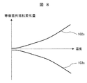
- FIG. 8 shows the temperature characteristics of the equivalent series resistance of the smoothing capacitor 43 and the smoothing capacitor 44.
- the vertical axis represents the change in equivalent series resistance, and the horizontal axis represents temperature.
- the equivalent series resistance of the smoothing capacitor 43 has a positive temperature characteristic 102c
- the equivalent series resistance of the smoothing capacitor 44 has a negative temperature characteristic 103c.
- the equivalent series resistance has a positive temperature characteristic
- the equivalent series resistance increases as the temperature rises. For this reason, the increase in the current flowing to the smoothing capacitor 43 is suppressed.
- the equivalent series resistance has a negative temperature characteristic
- the equivalent series resistance decreases as the temperature rises. For this reason, the decrease in the current flowing to the smoothing capacitor 44 is suppressed. Therefore, an increase in the current unbalance between the smoothing capacitor 43 and the smoothing capacitor 42 due to the difference between the positive and negative temperature characteristics of the capacitance is prevented.
- the smoothing capacitors 43 and 44 film capacitors having different dielectric film materials are applied as the smoothing capacitors having different temperature characteristics of capacitance and temperature characteristics of equivalent series resistance.
- the dielectric film material is appropriately selected from polypropylene, polyethylene terephthalate, polyphenylene sulfide, polyethylene and the like.
- a film capacitor using polypropylene as a dielectric film material is applied as the smoothing capacitor 43
- a film capacitor using polyethylene terephthalate as a dielectric film material is applied as the smoothing capacitor 44.
- electrolytic capacitors, ceramic capacitors, etc. may be applied as long as they are capacitors that can obtain positive / negative temperature characteristics of electrostatic capacitance and positive / negative temperature characteristics of equivalent series resistance.
- FIG. 9 shows a power converter according to a modification of the second embodiment.
- the present modification corresponds to the modification (FIG. 5) of the first embodiment described above.
- the power converter 101e (FIG. 9) has the same circuit configuration as that of the second embodiment (FIG. 7), but operates differently as the forward converter in the second embodiment. .
- FIG. 10 shows a power converter which is another modification of the second embodiment.
- the present modification corresponds to another modification (FIG. 6) of the first embodiment described above.
- the power conversion main circuit is a rectifier provided with a three-phase full bridge circuit consisting of diodes 9. Therefore, the power conversion device 101 f operates as a forward converter.
- smoothing capacitor group 4b in the modification of the second embodiment shown in FIGS. 9 and 10 has the same configuration as that of the second embodiment, the same effect as the second embodiment described above can be obtained also in these modifications. .
- Embodiment 2 of the present invention will be described, but mainly points different from Embodiments 1 and 2 will be described.
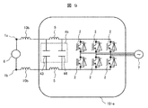
- FIG. 11 is a circuit diagram showing a configuration of a power conversion device according to a third embodiment of the present invention.
- the circuit configuration including the power conversion device 101g is the same as the first embodiment (FIG. 1) and the second embodiment (FIG. 7), but in the third embodiment, the smoothing capacitor group 4b and A voltage sensor 8 is connected between DC terminals 1 c and 1 d between the DC side of the power conversion main circuit consisting of the semiconductor switching element 2.
- the smoothing capacitor 45 in the smoothing capacitor group 4c has positive temperature characteristics and negative frequency characteristics in terms of electrostatic capacitance, as with the smoothing capacitor 41 in the first embodiment (FIG. 1). Further, the smoothing capacitor 46 in the smoothing capacitor group 4c has a negative temperature characteristic and a positive frequency characteristic in electrostatic capacitance, as with the smoothing capacitor 42 in the first embodiment (FIG. 1).
- the detection value of the voltage sensor 8 is used to control AC power output from the power conversion device 101g in a control device (not shown). Furthermore, in the third embodiment, as described later, when occurrence of current unbalance of the smoothing capacitors 45 and 46 is detected based on the detection value of the voltage sensor 8, the carrier frequency used for PWM control is increased. Thereby, the impedance of each smoothing capacitor is increased, and the magnitude of the ripple current flowing in each smoothing capacitor is suppressed. Therefore, excessive current unbalance can be prevented, and the life deterioration of each smoothing capacitor can be prevented.
- the voltage sensor 8 detects the DC voltage input voltage of the power conversion device 101g, that is, the voltage value of the smoothing capacitor group 4c.
- the control device (not shown) detects the magnitude of the voltage change of the smoothing capacitor group 4 c based on the voltage value detected by the voltage sensor 8.
- the magnitude of the voltage change of the smoothing capacitor group 4c indicates the speed of charging / discharging of the smoothing capacitor group 4c, and as shown by the above-mentioned equation (1), the magnitude of the total capacitance of the smoothing capacitor group 4c Change depending on In particular, when the total capacitance of the smoothing capacitor group 4c decreases and the ripple removal performance of the smoothing capacitor group 4c decreases, charging / discharging is accelerated, and the magnitude of the voltage change increases.
- control device determines whether or not the detected value of the magnitude of the voltage change of the smoothing capacitor group 4c exceeds the preset threshold value. It is determined whether or not the total capacitance of the capacitor is reduced, that is, whether the current imbalance of the smoothing capacitors 45 and 46 is generated as the temperature rises.
- FIG. 12 shows a carrier and a modulation wave used for PWM control (PWM: Pulse Width Modulation) of the power conversion device in the third embodiment.
- PWM Pulse Width Modulation
- a modulated wave 116 (voltage command) having a fundamental frequency as shown in FIG. 12 and a triangular wave carrier 117 having a frequency sufficiently higher than that of the modulated wave 116 and having a high frequency corresponding to the switching frequency of the semiconductor switching element 2
- a PWM pulse serving as a switching pattern of the semiconductor switching element 2 is generated.
- the PWM control in the third embodiment is a known technique, and further detailed description is omitted.
- FIG. 13 shows an equivalent circuit of a capacitor.
- the capacitor is represented by a series connection circuit of an internal inductance 113, a capacitance 114, and an equivalent series resistance 115 (ESR: Equivalent Series Resistance).
- ESR Equivalent Series Resistance
- the size of the internal inductance 113 mainly depends on the configuration of the metal conductor such as the internal electrode and the lead of the capacitor, so there is little temperature dependency and frequency dependency.
- the size of the capacitance 114 depends on the characteristics of the dielectric, it has frequency characteristics and temperature characteristics as in the third embodiment and the first and second embodiments.
- the equivalent series resistance 115 is composed of the electrical resistance components of the dielectric and the metal conductor, it has frequency characteristics and temperature characteristics as described in the second embodiment.
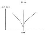
- FIG. 14 shows an example of the frequency characteristic of the impedance of the capacitor.
- the impedance Z of the capacitor is expressed by equation (2) from the equivalent circuit shown in FIG.
- R, L, and C indicate the equivalent series resistance 115, the internal inductance 113, and the electrostatic capacitance 114, respectively.
- ⁇ indicates an angular frequency.
- FIG. 14 shows an example of the relationship between the magnitude of Z and ⁇ expressed by the equation (2), that is, the RLC series resonance characteristic. Therefore, in the third embodiment, the impedances of the smoothing capacitors 45 and 46 have such resonance characteristics.
- the impedance increases as the frequency moves away from the resonance point.
- the reactance component by the electrostatic capacitance 114 is dominant on the low frequency side, and the reactance component by the internal inductance 113 is dominant on the high frequency side. Therefore, on the low frequency side, the difference in capacitance 114 of the capacitor has a large influence on the impedance. Therefore, when the capacitance of each smoothing capacitor varies as the temperature rises, the impedance of the smoothing capacitor is large even if the carrier frequency is lowered to increase the impedance of the smoothing capacitor. Because of variations, it is difficult to prevent current imbalance.
- the difference in the internal inductance 113 of the capacitor has a large influence on the impedance.
- the temperature dependency of the internal inductance 113 is small. Therefore, when variations occur in the capacitance of each smoothing capacitor as the temperature rises, the carrier frequency is made higher than usual to increase the size of the impedance of each smoothing capacitor, whereby the current flows in each smoothing capacitor. Since the magnitude of the ripple current is suppressed, it is possible to prevent excessive current unbalance.
- FIG. 15 is a circuit diagram showing a configuration of a power conversion device that is Embodiment 4 of the present invention.
- the power conversion device of the third embodiment is connected to an AC power system.
- the AC power system is indicated by the system power source 131 and the system inductance 131 and the parasitic capacitance 132 between the AC power source 7 and the power conversion device.
- the power conversion device of the present embodiment includes a power conversion main circuit configured of the semiconductor switching element 2 as in the first to third embodiments (FIGS. 1, 7 and 11).
- the direct current side of the power conversion circuit is connected to a storage device 4 for storing direct current power.
- the AC side of the power conversion main circuit is connected to an AC power system via a harmonic filter 119.
- the power conversion main circuit converts the AC power from the AC power system into DC power and stores the power in the power storage device 4 by controlling the semiconductor switching element 2 on and off, and AC powers the DC power from the power storage device 4 Convert to electric power and output to AC power system.
- the superposition of the harmonic current included in the AC power output from the power conversion device on the AC power system is suppressed by the harmonic filter 119.
- the harmonic filter 119 includes an LC filter circuit configured of a reactor connected in series and a filter capacitor connected to a series connection point of the reactors.
- the LC filter circuit includes a reactor 120 connected in series, and capacitors 121 and 122 connected between a series connection point of the reactor 120 and the ground 123.
- the capacitors 121 and 122 are connected in parallel to each other to form a filter capacitor.
- the capacitor 121 in the filter capacitor has positive temperature characteristics and negative frequency characteristics in terms of electrostatic capacitance, as with the smoothing capacitor 41 in the first embodiment (FIG. 1). Further, the capacitor 122 in the filter capacitor has negative temperature characteristics and positive frequency characteristics in terms of electrostatic capacitance, as with the smoothing capacitor 42 in the first embodiment (FIG. 1).
- the filter performance can be maintained against temperature fluctuation, and the life degradation of the harmonic filter due to the current unbalance can be prevented.
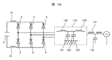
- FIG. 16 shows a power converter which is a modification of the fourth embodiment.
- points different from the fourth embodiment will be described.
- the power conversion main circuit is a rectifier provided with a three-phase full bridge circuit consisting of diodes 9. Accordingly, the power conversion device operates as a forward converter, converts AC power supplied from the power system into DC power, and stores the DC power in the storage device 4.
- the filter capacitor group in this modification has the same configuration as that of the fourth embodiment, the same effect as that of the first embodiment described above can be obtained in this modification as well.
- each of the capacitor 121 and the capacitor 121 described above has a positive temperature characteristic in electrostatic capacitance and a negative temperature dependency in equivalent series resistance and a negative capacitor.
- the effect similar to that of the fourth embodiment can be obtained also as a capacitor having a temperature characteristic and a positive temperature dependency on equivalent series resistance.
- a fifth embodiment of the present invention will next be described, mainly focusing on differences from the first to fourth embodiments.
- FIG. 17 is a circuit diagram showing a configuration of a power conversion device according to a fifth embodiment of the present invention.
- the power conversion device in the fifth embodiment operates as a three-phase inverter as in the first embodiment, but unlike the first embodiment (FIG. 1), the two smoothing capacitor groups 4a are two. It is connected in parallel.
- the smoothing capacitor 41 has positive temperature characteristics and negative frequency characteristics in capacitance
- the smoothing capacitor 42 has negative temperature characteristics in capacitance and It has positive frequency characteristics.
- the total capacitance as the entire smoothing capacitor can be increased by parallel connection of the smoothing capacitor group 4a, and the fluctuation of the total capacitance due to the temperature fluctuation can be suppressed. Further, since the current imbalance of each capacitor can be suppressed, the life deterioration as the whole smoothing capacitor can be suppressed.
- the two smoothing capacitor groups 4 a are connected in parallel to each other via the wiring inductance 5.
- the two smoothing capacitor groups 4a are arranged adjacent to each other, so the four smoothing capacitors in FIG. 17 are arranged adjacent to each other.
- a group of smoothing capacitors (four smoothing capacitors in FIG. 17) constituting two smoothing capacitor groups 4a includes two adjacent smoothing capacitors including smoothing capacitor 41 and smoothing capacitor 42. To be arranged.
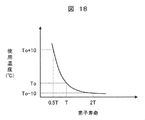
- FIG. 18 shows the relationship between the element life of the capacitor and the operating temperature.
- the element life of the capacitor is reduced by half when the operating temperature is increased by 10.degree.
- the lifetime of the capacitor is greatly influenced by the temperature.
- each smoothing capacitor When a plurality of smoothing capacitors are disposed adjacent to each other as in the fifth embodiment, the operating temperature of each smoothing capacitor affects not only self-heating and ambient temperature, but also the heating of other adjacent smoothing capacitors. Be done. For this reason, when heat generation of a certain smoothing capacitor is increased due to current concentration, not only the temperature of the smoothing capacitor rises but also the temperatures of other adjacent smoothing capacitors. For this reason, there is a possibility that the life deterioration as the whole of a plurality of smoothing capacitors may become large.
- each smoothing capacitor group 4a has a smoothing capacitor 41 having positive temperature characteristics and negative frequency characteristics in electrostatic capacity, and negative temperature characteristics and positive frequency characteristics in electrostatic capacity. Because the smoothing capacitor 42 has the following characteristics, fluctuations in the total capacitance of the plurality of smoothing capacitors as a whole are suppressed with respect to temperature fluctuations, and current concentration due to current imbalance and heat generation due to it are increased. Can be suppressed. Therefore, the life deterioration of the plurality of smoothing capacitors as a whole can be suppressed.
- FIG. 19 shows a power converter which is a modification of the fifth embodiment. Hereinafter, points different from the fifth embodiment will be described.
- the power conversion device (FIG. 19) has the same circuit configuration as that of the first embodiment (FIG. 1), but operates differently as the 19th embodiment as a forward converter.
- an AC power supply 7 is connected to the AC side of the power conversion main circuit formed of the semiconductor switching element 2, and two smoothing capacitor groups 4a and wiring inductance are connected to the DC side of the power conversion main circuit.
- the load 6 is connected via 10b.
- the power conversion device of this modification converts AC power supplied from the AC power supply 7 into DC power, and outputs this DC power to the load 6.
- AC power supply 7 is a three-phase AC power supply
- load 6 is a DC load.
- each smoothing capacitor group 4a in this modification has the same configuration as that of the fifth embodiment, the same effect as that of the above-mentioned fifth embodiment can be obtained also in this modification.
- FIG. 20 shows a power converter which is another modification of the fifth embodiment.
- points different from the fifth embodiment will be described.
- the power conversion main circuit is a rectifier provided with a three-phase full bridge circuit consisting of diodes 9. Therefore, the power conversion device of the present modification operates as a forward converter, converts AC power supplied from the AC power supply 7 into DC power, and outputs the DC power to the load 6.
- AC power supply 7 is a three-phase AC power supply
- load 6 is a DC load.
- each smoothing capacitor group 4a in this modification has the same configuration as that of the first embodiment, the same effect as that of the fifth embodiment described above can be obtained in this modification as well.
- the smoothing capacitor 41 and the smoothing capacitor 42 described above are respectively a capacitor having a positive temperature characteristic in electrostatic capacitance and a negative temperature dependence in equivalent series resistance.
- the effect similar to that of the fifth embodiment can be obtained also as a capacitor having negative temperature characteristics and positive temperature dependency in equivalent series resistance.
- the present invention is not limited to the embodiments described above, but includes various modifications.
- the embodiments described above are described in detail in order to explain the present invention in an easy-to-understand manner, and are not necessarily limited to those having all the configurations described.
- the number of paralleling smoothing capacitors and the number of paralleling smoothing capacitor groups may be any plural numbers.
- the voltage may be increased by configuring the above-mentioned smoothing capacitor by connecting a plurality of single capacitors in series.
Landscapes
- Engineering & Computer Science (AREA)
- Power Engineering (AREA)
- Inverter Devices (AREA)
Abstract
The present invention discloses a power conversion device in which fluctuation of capacitor capacitance due to temperature can be suppressed and current imbalance between capacitors can be suppressed. This power conversion device (101a) is provided with a power conversion main circuit, and a plurality of capacitors (41, 42) which are connected to the input or output side of the power conversion circuit and absorb harmonic currents. The plurality of capacitors include a first capacitor (41) and a second capacitor (42) which are connected in parallel with each other. The first capacitor (41) has a positive temperature characteristic in capacitance, and the second capacitor (42) has a negative temperature characteristic in capacitance. In addition, the first capacitor (41) has a negative frequency characteristic in capacitance, and the second capacitor (42) has a positive frequency characteristic in capacitance. Alternatively, the first capacitor (41) has a negative temperature characteristic in an equivalent series resistor, and the second capacitor (42) has a positive temperature characteristic in an equivalent series resistor.
Description
本発明は、平滑コンデンサを備える電力変換装置に関する。
The present invention relates to a power converter including a smoothing capacitor.
絶縁ゲート型バイポーラトランジスタ(IGBT)等の高速半導体スイッチング素子を用いた電力変換装置が様々な分野で使用されている。近年、半導体技術の進歩により大容量の半導体モジュールが実現され、大容量の電力変換装置の小型化が進んでいる。
Power converters using high-speed semiconductor switching devices such as insulated gate bipolar transistors (IGBTs) are used in various fields. 2. Description of the Related Art In recent years, advances in semiconductor technology have realized large-capacity semiconductor modules, and miniaturization of large-capacity power converters has progressed.
電力変換装置を大容量化するためには、半導体モジュールが複数並列接続される。この場合、電圧安定用の平滑コンデンサの充放電電流が大きくなるため、平滑コンデンサの電圧の変動が大きくなる。充放電電流を抑制するためには、コンデンサを複数並列接続して平滑コンデンサを構成することにより、平滑コンデンサの静電容量を増加させる。また、平滑用の小容量のコンデンサを備える変換器セルを複数並列接続して大容量の電力変換装置を構成することにより、コンデンサを並列接続して電力変換装置の平滑コンデンサの静電容量を増加する。
In order to increase the capacity of the power conversion device, a plurality of semiconductor modules are connected in parallel. In this case, since the charge / discharge current of the voltage stabilization smoothing capacitor becomes large, the fluctuation of the voltage of the smoothing capacitor becomes large. In order to suppress the charge and discharge current, the capacitance of the smoothing capacitor is increased by connecting a plurality of capacitors in parallel to configure the smoothing capacitor. Also, by connecting a plurality of converter cells provided with a small-capacity capacitor for smoothing in parallel to form a large-capacity power converter, the capacitors are connected in parallel to increase the capacitance of the smoothing capacitor of the power converter. Do.
複数のコンデンサが並列接続されると、コンデンサの静電容量とコンデンサ間の配線インダクタンスおよびコンデンサの内部インダクタンスによりLC共振現象が発生する可能性がある。共振周波数と、スイッチング素子のスイッチング周波数およびその整数倍の周波数が一致すると、共振経路のインピーダンスが小さくなり、コンデンサ電流が大幅に増大する。コンデンサ電流が増大すると、コンデンサの電力損失が大きくなったり、コンデンサの寿命が低下したりする。
When a plurality of capacitors are connected in parallel, LC resonance may occur due to the capacitance of the capacitors and the wiring inductance between the capacitors and the internal inductance of the capacitors. When the resonant frequency matches the switching frequency of the switching element and its integral multiple, the impedance of the resonant path decreases and the capacitor current increases significantly. As the capacitor current increases, the power loss of the capacitor increases and the life of the capacitor decreases.
このような共振現象に伴うコンデンサ電流の増大は、配線インダクタンスやスイッチング周波数の調整や最適化などによって抑制できる。しかし、コンデンサの静電容量に温度特性があるため、温度が変動すると共振周波数が変動して、コンデンサ電流が増大する怖れがある。また、静電容量の温度特性は、平滑コンデンサの静電容量自体を変動させる。
An increase in the capacitor current accompanying such a resonance phenomenon can be suppressed by adjusting or optimizing the wiring inductance or the switching frequency. However, since the capacitance of the capacitor has temperature characteristics, if the temperature changes, the resonance frequency may change, and the capacitor current may increase. In addition, the temperature characteristic of the capacitance causes the capacitance itself of the smoothing capacitor to fluctuate.
これに対し、平滑コンデンサの静電容量の温度変動を抑制する従来技術として、特許文献1に記載される技術が知られている。
On the other hand, the technique described in patent document 1 is known as a prior art which suppresses the temperature fluctuation of the electrostatic capacitance of a smoothing capacitor.
本技術では、温度上昇により静電容量が増大する正の温度特性を持つコンデンサと、温度上昇により静電容量が減少する負の温度特性を持つコンデンサが並列接続される。これにより、温度変化に対する静電容量の変化が相殺される。
In the present technology, a capacitor having a positive temperature characteristic in which capacitance increases with temperature rise and a capacitor having a negative temperature characteristic in which capacitance decreases with temperature rise are connected in parallel. This offsets the change in capacitance with changes in temperature.
上記の従来技術では、温度変化による平滑コンデンサの静電容量の変動は抑制できるが、個々のコンデンサの静電容量は異なるため、各コンデンサに流れる電流がアンバランスになる。このため、平滑コンデンサにおいて電流集中が生じるため、平滑コンデンサの寿命劣化を起こす恐れがある。
In the above-mentioned prior art, although the fluctuation of the capacitance of the smoothing capacitor due to the temperature change can be suppressed, since the capacitance of each capacitor is different, the current flowing to each capacitor becomes unbalanced. For this reason, since current concentration occurs in the smoothing capacitor, the life of the smoothing capacitor may be deteriorated.
そこで、本発明は、コンデンサの静電容量の温度による変動を抑制できるとともに、コンデンサにおける電流アンバランスを抑制できる電力変換装置を提供する。
Therefore, the present invention can provide a power conversion device capable of suppressing a variation in capacitance of a capacitor due to temperature and suppressing current imbalance in the capacitor.
上記課題を解決するために、本発明による電力変換装置は、電力変換回路の入力側もしくは出力側に接続され、高調波電流を吸収する複数のコンデンサと、を備えるものであって、複数のコンデンサは、互いに並列接続される第1のコンデンサおよび第2のコンデンサを含み、第1のコンデンサおよび第2のコンデンサは、静電容量と等価直列抵抗とインダクタンスとを成分とする内部インピーダンスを有し、第1のコンデンサは静電容量に正の温度特性を有し、第2のコンデンサは静電容量に負の温度特性を有し、さらに、第1のコンデンサおよび第2のコンデンサの温度変動に対する静電容量の変動に伴う、第1のコンデンサおよび第2のコンデンサにおける高調波電流のアンバランスの増大を、内部インピーダンスの成分のいずれかの変化によって緩和する。
In order to solve the above problems, a power conversion device according to the present invention comprises a plurality of capacitors connected to the input side or the output side of a power conversion circuit and absorbing harmonic current, and a plurality of capacitors Includes a first capacitor and a second capacitor connected in parallel to each other, and the first capacitor and the second capacitor have internal impedances having capacitances, equivalent series resistances and inductances, The first capacitor has positive temperature characteristics in terms of capacitance, and the second capacitor has negative temperature characteristics in terms of capacitance. Furthermore, the second capacitor has a static characteristic against temperature variations of the first capacitor and the second capacitor. An increase in the imbalance of the harmonic current in the first capacitor and the second capacitor due to the change in capacitance is either of the components of the internal impedance Mitigated by the change.
また、上記課題を解決するために、本発明による電力変換装置は、電力変換主回路と、電力変換回路の入力側もしくは出力側に接続され、高調波電流を吸収する複数のコンデンサと、を備えるものであって、複数のコンデンサは、互いに並列接続される第1のコンデンサおよび第2のコンデンサを含み、第1のコンデンサは静電容量に正の温度特性を有し、第2のコンデンサは静電容量に負の温度特性を有し、さらに、第1のコンデンサは静電容量に負の周波数特性を有し、第2のコンデンサは静電容量に正の周波数特性を有する。
Furthermore, in order to solve the above problems, a power conversion device according to the present invention includes a power conversion main circuit and a plurality of capacitors connected to the input side or the output side of the power conversion circuit and absorbing harmonic current. The plurality of capacitors include a first capacitor and a second capacitor connected in parallel with one another, the first capacitor having a positive temperature characteristic of capacitance, and the second capacitor being static. The capacitance has a negative temperature characteristic, the first capacitor has a negative frequency characteristic of the capacitance, and the second capacitor has a positive frequency characteristic of the capacitance.
また、上記課題を解決するために、電力変換主回路と、電力変換回路の入力側もしくは出力側に接続され、高調波電流を吸収する複数のコンデンサと、を備えるものであって、複数のコンデンサは、互いに並列接続される第1のコンデンサおよび第2のコンデンサを含み、第1のコンデンサは静電容量に正の温度特性を有し、第2のコンデンサは静電容量に負の温度特性を有し、さらに、第1のコンデンサは等価直列抵抗に負の温度特性を有し、第2のコンデンサは等価直列抵抗に正の温度特性を有する。
Furthermore, in order to solve the above problems, the power conversion main circuit, and a plurality of capacitors connected to the input side or the output side of the power conversion circuit and absorbing harmonic current, which are a plurality of capacitors Includes a first capacitor and a second capacitor connected in parallel with one another, the first capacitor having positive temperature characteristics in capacitance, and the second capacitor having negative temperature characteristics in capacitance Furthermore, the first capacitor has negative temperature characteristics in the equivalent series resistance, and the second capacitor has positive temperature characteristics in the equivalent series resistance.
本発明によれば、電力変換回路の入力側もしくは出力側に接続されるコンデンサの静電容量の温度による変動を抑制できるとともに、平滑コンデンサにおける電流アンバランスを抑制できる
上記した以外の課題、構成および効果は、以下の実施形態の説明により明らかにされる。 According to the present invention, it is possible to suppress the variation due to the temperature of the capacitance of the capacitor connected to the input side or the output side of the power conversion circuit, and to suppress the current unbalance in the smoothing capacitor. The effect is clarified by the following description of the embodiment.
上記した以外の課題、構成および効果は、以下の実施形態の説明により明らかにされる。 According to the present invention, it is possible to suppress the variation due to the temperature of the capacitance of the capacitor connected to the input side or the output side of the power conversion circuit, and to suppress the current unbalance in the smoothing capacitor. The effect is clarified by the following description of the embodiment.
本発明の一実施形態である電力変換装置は、電力変換用の半導体素子から構成される電力変換主回路と、電力変換回路の入力側もしくは出力側に接続され、高調波電流を吸収する複数のコンデンサ(例えば、平滑コンデンサやフィルタコンデンサ)を備える。この複数のコンデンサは、互いに並列接続される第1のコンデンサおよび第2のコンデンサを含み、これらのコンデンサは、静電容量と等価直列抵抗とインダクタンスとを成分とする内部インピーダンスを有する。なお、第1のコンデンサおよび第2のコンデンサの等価回路は、公知のコンデンサと同様に、これら成分の直列接続回路となる。
A power conversion device according to an embodiment of the present invention includes a power conversion main circuit including a semiconductor element for power conversion, and a plurality of power conversion circuits connected to the input side or the output side of the power conversion circuit to absorb harmonic currents. A capacitor (eg, a smoothing capacitor or a filter capacitor) is provided. The plurality of capacitors include a first capacitor and a second capacitor connected in parallel with one another, and these capacitors have internal impedances that are components of capacitance, equivalent series resistance and inductance. The equivalent circuit of the first capacitor and the second capacitor is, like the known capacitor, a series connection circuit of these components.
ここで、第1のコンデンサは静電容量に正の温度特性を有し、第2のコンデンサは静電容量に負の温度特性を有する。これにより、第1のコンデンサおよび第2のコンデンサの並列接続の総静電容量の温度変化が抑制される。従って、高調波電流を吸収する機能は変動することなく維持される。しかし、個々のコンデンサの静電容量の値は異なるため、第1のコンデンサと第2のコンデンサが吸収する高調波電流の大きさがばらつく怖れがある。
Here, the first capacitor has positive temperature characteristics in capacitance, and the second capacitor has negative temperature characteristics in capacitance. Thereby, the temperature change of the total capacitance of the parallel connection of the first capacitor and the second capacitor is suppressed. Thus, the ability to absorb harmonic currents is maintained without variation. However, since the capacitance value of each capacitor is different, there is a possibility that the magnitude of the harmonic current absorbed by the first capacitor and the second capacitor may vary.
そこで、本実施形態においては、第1のコンデンサおよび第2のコンデンサの温度変動に対する静電容量の変動に伴う、第1のコンデンサおよび第2のコンデンサにおける高調波電流のアンバランスの増大を、内部インピーダンスの成分、すなわち静電容量と等価直列抵抗とインダクタンスのいずれかの変化によって緩和する。
Therefore, in the present embodiment, the increase in the imbalance of the harmonic current in the first capacitor and the second capacitor due to the fluctuation of the capacitance with the temperature fluctuation of the first capacitor and the second capacitor is It is mitigated by the change of the impedance component, that is, the capacitance and either the equivalent series resistance or the inductance.
以下、本発明の実施形態について、下記の実施例1~5により、図面を用いながら、より具体的に説明する。各図において、参照番号が同一のものは同一の構成要件あるいは類似の機能を備えた構成要件を示している。
Hereinafter, embodiments of the present invention will be described more specifically by using the following Examples 1 to 5 with reference to the drawings. In the drawings, those with the same reference numerals indicate components having the same configuration or similar functions.
図1は、本発明の実施例1である電力変換装置の構成を示す回路図である。
FIG. 1 is a circuit diagram showing the configuration of a power conversion device according to a first embodiment of the present invention.
図1に示すように、電力変換装置101aにおいては、入力端子1a,1b間に直流電源1が接続され、この直流電源1に、半導体スイッチング素子2によって構成される電力変換主回路の直流側が、複数の平滑コンデンサ41,42を介して接続される。また、電力変換主回路の交流側、すなわち電力変換回路の出力は、負荷6に接続される。
As shown in FIG. 1, in the power conversion device 101a, the DC power supply 1 is connected between the input terminals 1a and 1b, and the DC side of the power conversion main circuit configured by the semiconductor switching element 2 is connected to the DC power supply 1. It is connected via a plurality of smoothing capacitors 41 and 42. Further, the AC side of the power conversion main circuit, that is, the output of the power conversion circuit is connected to the load 6.
なお、本実施例1において、平滑コンデンサ41は、静電容量に正の温度特性を有する。また、平滑コンデンサ41と並列に接続される平滑コンデンサ42は、静電容量に負の温度特性を有する。従って、本実施例においては、温度変化に伴う、平滑コンデンサ41および平滑コンデンサ42の静電容量の変化量の正負が互いに逆である。これにより、平滑コンデンサ41および平滑コンデンサ42の静電容量の変化量が、互いに相殺し合い、平滑コンデンサ群4aの総静電容量の値の温度変動が抑制される。例えば、各変化量の絶対値を実質同じ値にすれば、平滑コンデンサ群4aの総静電容量は、温度が変動しても、一定に保たれる。
In the first embodiment, the smoothing capacitor 41 has a positive temperature characteristic of electrostatic capacitance. The smoothing capacitor 42 connected in parallel to the smoothing capacitor 41 has a negative temperature characteristic of electrostatic capacitance. Therefore, in the present embodiment, the positive and negative values of the amount of change in capacitance of the smoothing capacitor 41 and the smoothing capacitor 42 with temperature change are opposite to each other. As a result, the amounts of change in the capacitances of the smoothing capacitor 41 and the smoothing capacitor 42 cancel each other out, and the temperature fluctuation of the value of the total capacitance of the smoothing capacitor group 4a is suppressed. For example, if the absolute value of each variation is made substantially the same, the total capacitance of the smoothing capacitor group 4a is kept constant even if the temperature fluctuates.
複数の平滑コンデンサ41,42は、配線インダクタンス5を介して、互いに並列に接続され、平滑コンデンサ群4aを構成する。実装状態では、平滑コンデンサ群4aを構成する平滑コンデンサ41,42は互いに隣接して配置される。
The plurality of smoothing capacitors 41 and 42 are connected in parallel with each other via the wiring inductance 5 to form a smoothing capacitor group 4 a. In the mounted state, the smoothing capacitors 41 and 42 constituting the smoothing capacitor group 4a are arranged adjacent to each other.
平滑コンデンサ群4aは、配線インダクタンス10aおよび入力端子1a,1bを介して直流電源1に接続される。従って、本実施例1では、平滑コンデンサ41は、配線インダクタンス5,10aの内、配線インダクタンス10aを介して直流電源に並列に接続され、配線インダクタンス5を介して電力変換主回路の直流側に並列に接続される。また、平滑コンデンサ42は、配線インダクタンス5,10aの内、配線インダクタンス5および10aを介して直流電源に並列に接続され、配線インダクタンス5および10aを介することなく電力変換主回路の直流側に並列に接続される。なお、本実施例において、配線インダクタンス5の値は、配線インダクタンス10aの値よりも十分小さい。すなわち、平滑コンデンサ41,42間の配線長は、平滑コンデンサ群4aと直流電源1との間の配線長よりも十分短い。
The smoothing capacitor group 4a is connected to the DC power supply 1 through the wiring inductance 10a and the input terminals 1a and 1b. Therefore, in the first embodiment, the smoothing capacitor 41 is connected in parallel to the DC power supply through the wiring inductance 10 a among the wiring inductances 5 and 10 a, and parallel to the DC side of the power conversion main circuit through the wiring inductance 5. Connected to Further, the smoothing capacitor 42 is connected in parallel to the DC power supply through the wiring inductance 5 and 10a among the wiring inductances 5 and 10a, and in parallel to the DC side of the power conversion main circuit without the wiring inductance 5 and 10a. Connected In the present embodiment, the value of the wiring inductance 5 is sufficiently smaller than the value of the wiring inductance 10a. That is, the wiring length between the smoothing capacitors 41 and 42 is sufficiently shorter than the wiring length between the smoothing capacitor group 4 a and the DC power supply 1.
なお、本実施例1において、電力変換主回路は、半導体スイッチング素子2からなる三相フルブリッジ回路を備える三相インバータであり、負荷6は、三相交流電動機などの三相交流負荷である。また、半導体スイッチング素子2としては、IGBT(Insulated Gate Bipolar Transistor)やMOSFET(Metal Oxide Semiconductor Field Effect Transistor)等が適用される(図1中には、IGBTを記す)。なお、図1中では、三相フルブリッジ回路の一つのアームが、一個の半導体スイッチング素子2から構成されているが、これに限らず、複数の半導体スイッチング素子の直並列接続から構成されても良い。
In the first embodiment, the power conversion main circuit is a three-phase inverter provided with a three-phase full bridge circuit formed of the semiconductor switching element 2, and the load 6 is a three-phase AC load such as a three-phase AC motor. Further, as the semiconductor switching element 2, an IGBT (Insulated Gate Bipolar Transistor), a MOSFET (Metal Oxide Semiconductor Field Effect Transistor), or the like is applied (in FIG. 1, the IGBT is described). In FIG. 1, one arm of the three-phase full bridge circuit is formed of one semiconductor switching element 2. However, the present invention is not limited to this. Even if a plurality of semiconductor switching elements are connected in series and parallel, good.
電力変換装置101aは、電力変換主回路を構成する半導体スイッチング素子2をPWM制御(PWM:Pulse Width Modulation)等のスイッチング制御によってオン・オフすることにより、直流電源1から供給される直流電力を交流電力へ変換し、この交流電力を負荷6に出力する。すなわち、電力変換装置101aは、逆変換器(インバータ)である。このとき、平滑コンデンサ群4にはリプル電流が流れるが、リプル電流の大きさは、平滑コンデンサ41の静電容量と、平滑コンデンサ42の静電容量、平滑コンデンサ41と平滑コンデンサ42間の配線インダクタンス5によるLC共振に依存する。
The power conversion device 101a turns DC power supplied from the DC power supply 1 into AC power by turning on / off the semiconductor switching element 2 constituting the power conversion main circuit by switching control such as PWM control (PWM: Pulse Width Modulation). It converts to electric power and outputs this AC power to the load 6. That is, the power conversion device 101a is an inverse converter (inverter). At this time, ripple current flows through the smoothing capacitor group 4, but the magnitude of the ripple current is determined by the capacitance of the smoothing capacitor 41, the capacitance of the smoothing capacitor 42, and the wiring inductance between the smoothing capacitor 41 and the smoothing capacitor 42. 5 depends on LC resonance.
図2は、LC共振の周波数特性を示す。半導体スイッチング素子2のスイッチング周波数が、共振周波数118に一致すると、平滑コンデンサ群4aには大きなリプル電流が流れる。リプル電流が増大すると、コンデンサ温度が上昇する。このため、静電容量に正の温度特性を有する平滑コンデンサ41は静電容量が増大する。また、静電容量に負の温度特性を有する平滑コンデンサ42は静電容量が減少する。
FIG. 2 shows frequency characteristics of LC resonance. When the switching frequency of the semiconductor switching element 2 matches the resonant frequency 118, a large ripple current flows in the smoothing capacitor group 4a. As the ripple current increases, the capacitor temperature rises. For this reason, in the smoothing capacitor 41 having a positive temperature characteristic in electrostatic capacitance, the electrostatic capacitance is increased. In addition, the smoothing capacitor 42 having a negative temperature characteristic in electrostatic capacitance reduces the electrostatic capacitance.
ここで、コンデンサ電流iは、静電容量をCとし、コンデンサ電圧をVとして、式(1)によって表される。dV/dtはコンデンサ電圧の時間変化率を示す。
Here, the capacitor current i is represented by the equation (1), where C is a capacitance and V is a capacitor voltage. dV / dt represents the time rate of change of the capacitor voltage.

このような電流のアンバランスは、半導体スイッチング素子2のスイッチング周波数が、平滑コンデンサ群4aにおけるLC共振の共振周波数に近い場合に顕著になる。これは、温度上昇によって平滑コンデンサ41および平滑コンデンサ42の静電容量の値に差異が生じるのに加えて、半導体スイッチング素子2のスイッチングに伴って平滑コンデンサ41,42に流れるリプル電流における共振周波数に近い周波数成分が多くなるためである。電流のアンバランスが顕著になると、平滑コンデンサ41に電流集中が起きるので、平滑コンデンサ41の寿命が低下する怖れがある。
Such unbalance of the current becomes remarkable when the switching frequency of the semiconductor switching element 2 is close to the resonance frequency of the LC resonance in the smoothing capacitor group 4a. This is because, in addition to the difference in the capacitance values of the smoothing capacitor 41 and the smoothing capacitor 42 due to the temperature rise, the resonance frequency in the ripple current flowing in the smoothing capacitors 41 and 42 along with the switching of the semiconductor switching element 2 This is because close frequency components are increased. If the imbalance of the current becomes significant, current concentration occurs in the smoothing capacitor 41, and the life of the smoothing capacitor 41 may be reduced.
これに対し、本実施例1においては、以下に説明するように、平滑コンデンサ41および平滑コンデンサ42の特性を異ならしめる。
On the other hand, in the first embodiment, the characteristics of the smoothing capacitor 41 and the smoothing capacitor 42 are made different as described below.
図3は、平滑コンデンサ41と平滑コンデンサ42の静電容量の温度特性を示す。なお、縦軸は静電容量の変化分を示し、横軸は温度を示す。
FIG. 3 shows temperature characteristics of the capacitances of the smoothing capacitor 41 and the smoothing capacitor 42. The vertical axis represents the change in capacitance, and the horizontal axis represents temperature.
図3に示すように、平滑コンデンサ41の静電容量は正の温度特性102bを有し、平滑コンデンサ42の静電容量は負の温度特性102aを示す。
As shown in FIG. 3, the capacitance of the smoothing capacitor 41 has a positive temperature characteristic 102b, and the capacitance of the smoothing capacitor 42 has a negative temperature characteristic 102a.
図4は、平滑コンデンサ41と平滑コンデンサ42の静電容量の周波数特性を示す。なお、縦軸は静電容量の変化分を示し、横軸は周波数を示す。
FIG. 4 shows frequency characteristics of the capacitances of the smoothing capacitor 41 and the smoothing capacitor 42. The vertical axis indicates the change in capacitance, and the horizontal axis indicates the frequency.
図4に示すように、平滑コンデンサ41の静電容量は負の周波数特性103bを有し、平滑コンデンサ42の静電容量は正の周波数特性103aを示す。
As shown in FIG. 4, the capacitance of the smoothing capacitor 41 has a negative frequency characteristic 103b, and the capacitance of the smoothing capacitor 42 shows a positive frequency characteristic 103a.
このように、平滑コンデンサ41の静電容量は、正の温度特性および負の周波数特性を有するため、温度上昇による静電容量の増大が、共振周波数に近い高周波数においては、負の周波数特性による静電容量の減少によって相殺される。このため、平滑コンデンサ41に流れる電流の増大が抑制される。また、平滑コンデンサ42の静電容量は、負の温度特性および正の周波数を有するため、温度上昇による静電容量の減少が、共振周波数に近い高周波数においては、正の周波数特性による静電容量の増大によって相殺される。このため、平滑コンデンサ41に流れる電流の減少が抑制される。このため、平滑コンデンサ41と平滑コンデンサ42の電流アンバランスの増大が防止される。
As described above, since the capacitance of the smoothing capacitor 41 has positive temperature characteristics and negative frequency characteristics, the increase in capacitance due to temperature rise is due to the negative frequency characteristics at high frequencies close to the resonance frequency. It is offset by the decrease in capacitance. For this reason, the increase in the current flowing to the smoothing capacitor 41 is suppressed. In addition, since the capacitance of the smoothing capacitor 42 has negative temperature characteristics and a positive frequency, the decrease in the capacitance due to temperature rise is caused by the positive frequency characteristics at high frequencies close to the resonance frequency. Offset by an increase in For this reason, a reduction in the current flowing to the smoothing capacitor 41 is suppressed. For this reason, the increase in current unbalance between the smoothing capacitor 41 and the smoothing capacitor 42 is prevented.
上述のような平滑コンデンサ41,42のように、静電容量の温度特性および周波数特性が互いに異なる平滑コンデンサとしては、誘電体フィルム材料が互いに異なるフィルムコンデンサが適用される。誘電体フィルム材料は、ポリプロピレン(polypropylene)、ポリエチレンテレフタラート(polyethylene terephthalate)、ポリフェニレンサルファルド(polyphenylene sulfide)、ポリエチレン(polyethylene)、ポリエステル(polyester)などから適宜選択される。例えば、平滑コンデンサ41としては、ポリプロピレンを誘電体フィルム材料とするフィルムコンデンサが適用され、平滑コンデンサ42としては、ポリエチレンテレフタラートを誘電体フィルム材料としたフィルムコンデンサが適用される。なお、これらのフィルムコンデンサに限らず、静電容量の正負の温度特性および周波数特性が得られるコンデンサであれば、電解コンデンサやセラミックコンデンサなどを適用しても良い。
As the smoothing capacitors 41 and 42 as described above, film capacitors having different dielectric film materials are applied as the smoothing capacitors having different temperature characteristics and frequency characteristics of capacitance. The dielectric film material is appropriately selected from polypropylene, polyethylene terephthalate, polyphenylene sulfide, polyethylene, polyester and the like. For example, a film capacitor using polypropylene as a dielectric film material is applied as the smoothing capacitor 41, and a film capacitor using polyethylene terephthalate as a dielectric film material is applied as the smoothing capacitor 42. An electrolytic capacitor, a ceramic capacitor, or the like may be applied as long as it is a capacitor that can obtain temperature characteristics and frequency characteristics of positive and negative electrostatic capacitances as well as the film capacitors.
なお、フィルムコンデンサは、一般に、比較的耐電圧が高く、低損失である。このような特徴は、電力変換装置に好適である。しかし、フィルムコンデンサは、静電容量に温度特性を有する。従って、本実施例1は、特に、フィルムコンデンサが適用される場合に、好適である(後述の、各実施例および各変形例についても、同様)。
In general, a film capacitor has a relatively high withstand voltage and low loss. Such a feature is suitable for a power converter. However, film capacitors have temperature characteristics of capacitance. Therefore, the first embodiment is particularly suitable when a film capacitor is applied (the same applies to each embodiment and each modification described later).
図5は、実施例1の変形例である電力変換装置を示す。以下、実施例1と異なる点について、説明する。なお、配線インダクタンス5のインダクタンスの値は、実施例1(図1)と同様に、配線インダクタンス10b(図1における配線インダクタンス10aに対応)の値よりも十分小さい(後述の図6の変形例も同様)。
FIG. 5 shows a power converter according to a modification of the first embodiment. Hereinafter, differences from the first embodiment will be described. As in the first embodiment (FIG. 1), the value of the inductance of the wiring inductance 5 is sufficiently smaller than the value of the wiring inductance 10b (corresponding to the wiring inductance 10a in FIG. 1). As well).
本変形例において、電力変換装置101b(図5)は、回路構成は実施例1(図1)と同様であるが、実施例1とは異なり順変換器として動作する。
In the present modification, the power conversion device 101b (FIG. 5) has the same circuit configuration as that of the first embodiment (FIG. 1), but operates differently as the first embodiment and operates as a forward converter.
図5に示すように、半導体スイッチング素子2から構成される電力変換主回路の交流側には交流電源7が接続され、電力変換主回路の直流側には平滑コンデンサ群4aおよび配線インダクタンス10bを介して負荷6が接続される。
As shown in FIG. 5, an AC power supply 7 is connected to the AC side of the power conversion main circuit composed of the semiconductor switching element 2, and the DC side of the power conversion main circuit is through the smoothing capacitor group 4a and the wiring inductance 10b. Load 6 is connected.
電力変換装置101bは、交流電源7から供給される交流電力を直流電力へ変換し、この直流電力を負荷6に出力する。なお、本変形例において、交流電源7は三相交流電源であり、負荷6は直流負荷である。
The power conversion device 101 b converts AC power supplied from the AC power supply 7 into DC power, and outputs the DC power to the load 6. In this modification, AC power supply 7 is a three-phase AC power supply, and load 6 is a DC load.
本変形例における平滑コンデンサ群4aは、実施例1と同様の構成を有するので、本変形例においても、上述の実施例1と同様の効果が得られる。
Since the smoothing capacitor group 4a in this modification has the same configuration as that of the first embodiment, the same effect as that of the above-described first embodiment can be obtained in this modification as well.
図6は、実施例1の他の変形例である電力変換装置を示す。以下、実施例1と異なる点について、説明する。
FIG. 6 shows a power converter according to another modification of the first embodiment. Hereinafter, differences from the first embodiment will be described.
図6に示すように、本変形例において、電力変換主回路は、ダイオード9からなる三相フルブリッジ回路を備える整流器である。従って、電力変換装置101cは、順変換器として動作し、交流電源7から供給される交流電力を直流電力へ変換し、この直流電力を負荷6に出力する。なお、本変形例において、交流電源7は三相交流電源であり、負荷6は直流負荷である。
As shown in FIG. 6, in the present variation, the power conversion main circuit is a rectifier provided with a three-phase full bridge circuit consisting of diodes 9. Therefore, the power conversion device 101 c operates as a forward converter, converts alternating current power supplied from the alternating current power supply 7 into direct current power, and outputs the direct current power to the load 6. In this modification, AC power supply 7 is a three-phase AC power supply, and load 6 is a DC load.
本変形例における平滑コンデンサ群4aは、実施例1と同様の構成を有するので、本変形例においても、上述の実施例1と同様の効果が得られる。
Since the smoothing capacitor group 4a in this modification has the same configuration as that of the first embodiment, the same effect as that of the above-described first embodiment can be obtained in this modification as well.
次に、本発明の実施例2について説明するが、主に、実施例1と異なる点について説明する。
Next, Embodiment 2 of the present invention will be described, but mainly points different from Embodiment 1 will be described.
図7は、本発明の実施例2である電力変換装置の構成を示す回路図である。
FIG. 7 is a circuit diagram showing a configuration of a power conversion device according to a second embodiment of the present invention.
図7に示すように、平滑コンデンサ群4bにおいて、平滑コンデンサ43および平滑コンデンサ44が、配線インダクタンス5を介して並列に接続される。実施例1と同様に、平滑コンデンサ43は静電容量に正の温度特性を有し、平滑コンデンサ44は静電容量に負の温度特性を有する。このため、実施例1と同様に、平滑コンデンサ群4bとしては、総静電容量の温度変化が抑制される。さらに、本実施例2において、平滑コンデンサ43,44は、後述するように、コンデンサの等価直列抵抗の温度特性が互いに異なっている。なお、平滑コンデンサ群4b以外の電力変換装置101dの回路構成は、実施例1(図1)と同様である。
As shown in FIG. 7, in the smoothing capacitor group 4 b, the smoothing capacitor 43 and the smoothing capacitor 44 are connected in parallel via the wiring inductance 5. As in the first embodiment, the smoothing capacitor 43 has positive temperature characteristics in terms of electrostatic capacitance, and the smoothing capacitor 44 has negative temperature characteristics in terms of electrostatic capacitance. For this reason, as in the first embodiment, the temperature change of the total capacitance is suppressed as the smoothing capacitor group 4b. Furthermore, in the second embodiment, as described later, the temperature characteristics of the equivalent series resistance of the smoothing capacitors 43 and 44 are different from each other. The circuit configuration of the power conversion device 101d other than the smoothing capacitor group 4b is the same as that of the first embodiment (FIG. 1).
図8は、平滑コンデンサ43と平滑コンデンサ44の等価直列抵抗の温度特性を示す。なお、縦軸は等価直列抵抗の変化分を示し、横軸は温度を示す。
FIG. 8 shows the temperature characteristics of the equivalent series resistance of the smoothing capacitor 43 and the smoothing capacitor 44. The vertical axis represents the change in equivalent series resistance, and the horizontal axis represents temperature.
図8に示すように、平滑コンデンサ43の等価直列抵抗は正の温度特性102cを有し、平滑コンデンサ44の等価直列抵抗は負の温度特性103cを有する。
As shown in FIG. 8, the equivalent series resistance of the smoothing capacitor 43 has a positive temperature characteristic 102c, and the equivalent series resistance of the smoothing capacitor 44 has a negative temperature characteristic 103c.
図8に示すように、平滑コンデンサ43においては、等価直列抵抗が正の温度特性を有するので、温度が上昇すると等価直列抵抗が増大する。このため、平滑コンデンサ43に流れる電流の増大が抑制される。また、平滑コンデンサ44においては、等価直列抵抗が負の温度特性を有するので、温度が上昇すると等価直列抵抗が減少する。このため、平滑コンデンサ44に流れる電流の減少が抑制される。従って、静電容量の温度特性の正負の違いに伴う、平滑コンデンサ43と平滑コンデンサ42の電流アンバランスの増大が防止される。
As shown in FIG. 8, in the smoothing capacitor 43, since the equivalent series resistance has a positive temperature characteristic, the equivalent series resistance increases as the temperature rises. For this reason, the increase in the current flowing to the smoothing capacitor 43 is suppressed. Further, in the smoothing capacitor 44, since the equivalent series resistance has a negative temperature characteristic, the equivalent series resistance decreases as the temperature rises. For this reason, the decrease in the current flowing to the smoothing capacitor 44 is suppressed. Therefore, an increase in the current unbalance between the smoothing capacitor 43 and the smoothing capacitor 42 due to the difference between the positive and negative temperature characteristics of the capacitance is prevented.
上述のような平滑コンデンサ43,44のように、静電容量の温度特性および等価直列抵抗の温度特性が互いに異なる平滑コンデンサとしては、誘電体フィルム材料が互いに異なるフィルムコンデンサが適用される。実施例1と同様に、誘電体フィルム材料は、ポリプロピレン、ポリエチレンテレフタラート、ポリフェニレンサルファルド、ポリエチレンなどから適宜選択される。例えば、平滑コンデンサ43としては、ポリプロピレンを誘電体フィルム材料とするフィルムコンデンサが適用され、平滑コンデンサ44としては、ポリエチレンテレフタラートを誘電体フィルム材料としたフィルムコンデンサが適用される。なお、これらのフィルムコンデンサに限らず、静電容量の正負の温度特性および等価直列抵抗の正負の温度特性が得られるコンデンサであれば、電解コンデンサやセラミックコンデンサなどを適用しても良い。
As the smoothing capacitors 43 and 44 as described above, film capacitors having different dielectric film materials are applied as the smoothing capacitors having different temperature characteristics of capacitance and temperature characteristics of equivalent series resistance. As in Example 1, the dielectric film material is appropriately selected from polypropylene, polyethylene terephthalate, polyphenylene sulfide, polyethylene and the like. For example, a film capacitor using polypropylene as a dielectric film material is applied as the smoothing capacitor 43, and a film capacitor using polyethylene terephthalate as a dielectric film material is applied as the smoothing capacitor 44. In addition to these film capacitors, electrolytic capacitors, ceramic capacitors, etc. may be applied as long as they are capacitors that can obtain positive / negative temperature characteristics of electrostatic capacitance and positive / negative temperature characteristics of equivalent series resistance.
図9は、実施例2の変形例である電力変換装置を示す。なお、本変形例は、前述の実施例1の変形例(図5)に対応する。
FIG. 9 shows a power converter according to a modification of the second embodiment. The present modification corresponds to the modification (FIG. 5) of the first embodiment described above.
図9に示すように、本変形例において、電力変換装置101e(図9)は、回路構成は実施例2(図7)と同様であるが、実施例2とは異なり順変換器として動作する。
As shown in FIG. 9, in this modification, the power converter 101e (FIG. 9) has the same circuit configuration as that of the second embodiment (FIG. 7), but operates differently as the forward converter in the second embodiment. .
図10は、実施例2の他の変形例である電力変換装置を示す。なお、本変形例は、前述の実施例1の他の変形例(図6)に対応する。
FIG. 10 shows a power converter which is another modification of the second embodiment. The present modification corresponds to another modification (FIG. 6) of the first embodiment described above.
図10に示すように、本変形例において、電力変換主回路は、ダイオード9からなる三相フルブリッジ回路を備える整流器である。従って、電力変換装置101fは、順変換器として動作する。
As shown in FIG. 10, in this modification, the power conversion main circuit is a rectifier provided with a three-phase full bridge circuit consisting of diodes 9. Therefore, the power conversion device 101 f operates as a forward converter.
これら図9および図10に示す実施例2の変形例における平滑コンデンサ群4bは、実施例2と同様の構成を有するので、これら変形例においても、上述の実施例2と同様の効果が得られる。
Since smoothing capacitor group 4b in the modification of the second embodiment shown in FIGS. 9 and 10 has the same configuration as that of the second embodiment, the same effect as the second embodiment described above can be obtained also in these modifications. .
次に、本発明の実施例2について説明するが、主に、実施例1,2と異なる点について説明する。
Next, Embodiment 2 of the present invention will be described, but mainly points different from Embodiments 1 and 2 will be described.
図11は、本発明の実施例3である電力変換装置の構成を示す回路図である。
FIG. 11 is a circuit diagram showing a configuration of a power conversion device according to a third embodiment of the present invention.
図11に示すように、電力変換装置101gを含む回路構成は、実施例1(図1)および実施例2(図7)と同様であるが、本実施例3においては、平滑コンデンサ群4bと、半導体スイッチング素子2からなる電力変換主回路の直流側との間における直流端子1c,1d間に電圧センサ8が接続される。
As shown in FIG. 11, the circuit configuration including the power conversion device 101g is the same as the first embodiment (FIG. 1) and the second embodiment (FIG. 7), but in the third embodiment, the smoothing capacitor group 4b and A voltage sensor 8 is connected between DC terminals 1 c and 1 d between the DC side of the power conversion main circuit consisting of the semiconductor switching element 2.
なお、平滑コンデンサ群4cにおける平滑コンデンサ45は、実施例1(図1)における平滑コンデンサ41と同様に、静電容量に正の温度特性および負の周波数特性を有する。また、平滑コンデンサ群4cにおける平滑コンデンサ46は、実施例1(図1)における平滑コンデンサ42と同様に、静電容量に負の温度特性および正の周波数特性を有する。
The smoothing capacitor 45 in the smoothing capacitor group 4c has positive temperature characteristics and negative frequency characteristics in terms of electrostatic capacitance, as with the smoothing capacitor 41 in the first embodiment (FIG. 1). Further, the smoothing capacitor 46 in the smoothing capacitor group 4c has a negative temperature characteristic and a positive frequency characteristic in electrostatic capacitance, as with the smoothing capacitor 42 in the first embodiment (FIG. 1).
電圧センサ8の検出値は、図示しない制御装置において、電力変換装置101gが出力する交流電力を制御するために用いられる。さらに、本実施例3においては、後述するように、電圧センサ8の検出値に基づき、平滑コンデンサ45,46の電流アンバランスの発生を検知したら、PWM制御に用いるキャリア周波数を増大する。これにより、各平滑コンデンサのインピーダンスを増大させ、各平滑コンデンサに流れるリプル電流の大きさを抑制する。従って、過度な電流アンバランスが防止され、各平滑コンデンサの寿命劣化を防止することができる。
The detection value of the voltage sensor 8 is used to control AC power output from the power conversion device 101g in a control device (not shown). Furthermore, in the third embodiment, as described later, when occurrence of current unbalance of the smoothing capacitors 45 and 46 is detected based on the detection value of the voltage sensor 8, the carrier frequency used for PWM control is increased. Thereby, the impedance of each smoothing capacitor is increased, and the magnitude of the ripple current flowing in each smoothing capacitor is suppressed. Therefore, excessive current unbalance can be prevented, and the life deterioration of each smoothing capacitor can be prevented.
まず、電圧センサ8による、平滑コンデンサ45,46の電流アンバランスの発生の検知について説明する。
First, the detection of the occurrence of the current unbalance of the smoothing capacitors 45 and 46 by the voltage sensor 8 will be described.
電圧センサ8は、電力変換装置101gの直流電圧入力電圧、すなわち平滑コンデンサ群4cの電圧値を検出する。図示しない制御装置は、電圧センサ8によって検出される電圧値に基づいて、平滑コンデンサ群4cの電圧変化の大きさを検出する。
The voltage sensor 8 detects the DC voltage input voltage of the power conversion device 101g, that is, the voltage value of the smoothing capacitor group 4c. The control device (not shown) detects the magnitude of the voltage change of the smoothing capacitor group 4 c based on the voltage value detected by the voltage sensor 8.
ここで、平滑コンデンサ群4cの電圧変化の大きさは、平滑コンデンサ群4cの充放電の速さを示し、前述の式(1)が示すように、平滑コンデンサ群4cの総静電容量の大きさによって変化する。特に、平滑コンデンサ群4cの総静電容量が減少して、平滑コンデンサ群4cのリプル除去性能が低下する場合には、充放電が速まるので、電圧変化の大きさが増加する。
Here, the magnitude of the voltage change of the smoothing capacitor group 4c indicates the speed of charging / discharging of the smoothing capacitor group 4c, and as shown by the above-mentioned equation (1), the magnitude of the total capacitance of the smoothing capacitor group 4c Change depending on In particular, when the total capacitance of the smoothing capacitor group 4c decreases and the ripple removal performance of the smoothing capacitor group 4c decreases, charging / discharging is accelerated, and the magnitude of the voltage change increases.
そこで、本実施例3においては、図示しない制御装置が、平滑コンデンサ群4cの電圧変化の大きさの検出値が予め設定される閾値を超えているか否かを判定することにより、平滑コンデンサ群4cの総静電容量が減少しているか否か、すなわち温度上昇に伴い平滑コンデンサ45,46の電流アンバランスが発生する状態であるか否かを判定する。
Therefore, in the third embodiment, the control device (not shown) determines whether or not the detected value of the magnitude of the voltage change of the smoothing capacitor group 4c exceeds the preset threshold value. It is determined whether or not the total capacitance of the capacitor is reduced, that is, whether the current imbalance of the smoothing capacitors 45 and 46 is generated as the temperature rises.
次に、電流アンバランスが検知される場合における各平滑コンデンサのインピーダンスを増大について説明する。
Next, the increase of the impedance of each smoothing capacitor when current imbalance is detected will be described.
図12は、本実施例3において電力変換装置のPWM制御(PWM:Pulse Width Modulation)に用いられるキャリアと変調波を示す。
FIG. 12 shows a carrier and a modulation wave used for PWM control (PWM: Pulse Width Modulation) of the power conversion device in the third embodiment.
図12に示すような基本周波数を有する変調波116(電圧指令)と、変調波116よりも十分に高い周波数であり、半導体スイッチング素子2のスイッチング周波数に対応する高周波数を有する三角波キャリア117とを比較することにより、半導体スイッチング素子2のスイッチングパターンとなるPWMパルスが生成される。なお、本実施例3におけるPWM制御は公知技術であり、さらに詳細な説明は省略する。
A modulated wave 116 (voltage command) having a fundamental frequency as shown in FIG. 12 and a triangular wave carrier 117 having a frequency sufficiently higher than that of the modulated wave 116 and having a high frequency corresponding to the switching frequency of the semiconductor switching element 2 By comparison, a PWM pulse serving as a switching pattern of the semiconductor switching element 2 is generated. The PWM control in the third embodiment is a known technique, and further detailed description is omitted.
図12に示す三角波キャリア117の周波数、すなわち半導体スイッチング素子2のスイッチング周波数に相当する高周波数成分を含むリプル電流が、各平滑コンデンサに流れる。
A ripple current including a high frequency component corresponding to the frequency of the triangular wave carrier 117 shown in FIG. 12, that is, the switching frequency of the semiconductor switching element 2 flows to each smoothing capacitor.
図13は、コンデンサの等価回路を示す。
FIG. 13 shows an equivalent circuit of a capacitor.
図13に示すように、コンデンサは、内部インダクタンス113と、静電容量114と、等価直列抵抗115(ESR:Equivalent Series Resistance)の直列接続回路によって表わされる。内部インダクタンス113の大きさは、主にコンデンサの内部電極やリードなどの金属導体の構成に依存するので、温度依存性や周波数依存性は少ない。静電容量114の大きさは、誘電体の特性に依存するので、本実施例3および前述の実施例1,2のように、周波数特性や温度特性を有する。等価直列抵抗115は、誘電体および金属導体の電気抵抗成分から構成されるので、周波数特性や、前述の実施例2のように温度特性を有する。
As shown in FIG. 13, the capacitor is represented by a series connection circuit of an internal inductance 113, a capacitance 114, and an equivalent series resistance 115 (ESR: Equivalent Series Resistance). The size of the internal inductance 113 mainly depends on the configuration of the metal conductor such as the internal electrode and the lead of the capacitor, so there is little temperature dependency and frequency dependency. Since the size of the capacitance 114 depends on the characteristics of the dielectric, it has frequency characteristics and temperature characteristics as in the third embodiment and the first and second embodiments. Since the equivalent series resistance 115 is composed of the electrical resistance components of the dielectric and the metal conductor, it has frequency characteristics and temperature characteristics as described in the second embodiment.
図14は、コンデンサのインピーダンスの周波数特性の一例を示す。
FIG. 14 shows an example of the frequency characteristic of the impedance of the capacitor.
コンデンサのインピーダンスZは、図13に示す等価回路から、式(2)で表される。
The impedance Z of the capacitor is expressed by equation (2) from the equivalent circuit shown in FIG.

図14は、式(2)で表されるZの大きさとωとの関係、すなわちRLC直列共振特性の一例を示している。従って、本実施例3においては、平滑コンデンサ45,46の各インピーダンスがこのような共振特性を有している。
FIG. 14 shows an example of the relationship between the magnitude of Z and ω expressed by the equation (2), that is, the RLC series resonance characteristic. Therefore, in the third embodiment, the impedances of the smoothing capacitors 45 and 46 have such resonance characteristics.
図14が示すように、周波数が共振点から離れると、インピーダンスは増大する。但し、式(2)から判るように、インピーダンスの大きさにおいて、低周波側では静電容量114によるリアクタンス成分が支配的になり、高周波側では内部インダクタンス113によるリアクタンス成分が支配的になる。そのため、低周波側ではコンデンサの静電容量114の違いがインピーダンスに与える影響が大きい。従って、温度上昇に伴って各平滑コンデンサの静電容量にばらつきが生じる場合、キャリアの周波数を通常よりも下げて平滑コンデンサのインピーダンスの大きさを増大させても、平滑コンデンサのインピーダンスの大きさがばらつくので、電流アンバランスを防止することが難しい。
As shown in FIG. 14, the impedance increases as the frequency moves away from the resonance point. However, as understood from the equation (2), in the magnitude of impedance, the reactance component by the electrostatic capacitance 114 is dominant on the low frequency side, and the reactance component by the internal inductance 113 is dominant on the high frequency side. Therefore, on the low frequency side, the difference in capacitance 114 of the capacitor has a large influence on the impedance. Therefore, when the capacitance of each smoothing capacitor varies as the temperature rises, the impedance of the smoothing capacitor is large even if the carrier frequency is lowered to increase the impedance of the smoothing capacitor. Because of variations, it is difficult to prevent current imbalance.
これに対し、高周波側ではコンデンサの内部インダクタンス113の違いがインピーダンスに与える影響が大きい。しかも、上述のように、内部インダクタンス113の温度依存性は小さい。従って、温度上昇に伴って各平滑コンデンサの静電容量にばらつきが生じる場合、キャリアの周波数を通常よりも高くして、各平滑コンデンサのインピーダンスの大きさを増大させることにより、各平滑コンデンサに流れるリプル電流の大きさが抑制されるので、過度な電流アンバランスを防止することができる。
On the other hand, on the high frequency side, the difference in the internal inductance 113 of the capacitor has a large influence on the impedance. Moreover, as described above, the temperature dependency of the internal inductance 113 is small. Therefore, when variations occur in the capacitance of each smoothing capacitor as the temperature rises, the carrier frequency is made higher than usual to increase the size of the impedance of each smoothing capacitor, whereby the current flows in each smoothing capacitor. Since the magnitude of the ripple current is suppressed, it is possible to prevent excessive current unbalance.
なお、実施例3における平滑コンデンサ群4cを、実施例2における平滑コンデンサ群4bように、静電容量に正の温度特性を有するとともに等価直列抵抗に負の温度依存性を有する平滑コンデンサと、静電容量に負の温度特性を有するとともに等価直列抵抗に正の温度依存性を有する平滑コンデンサとで構成しても、本実施例3と同様の効果が得られる。
As in the case of the smoothing capacitor group 4c in the third embodiment, as in the smoothing capacitor group 4b in the second embodiment, a smoothing capacitor having a positive temperature characteristic in electrostatic capacitance and a negative temperature dependency in equivalent series resistance, and a static capacitor Even if it has a negative temperature characteristic in capacitance and a smoothing capacitor having positive temperature dependence in equivalent series resistance, the same effect as that of the third embodiment can be obtained.
次に、本発明の実施例4について説明するが、主に、実施例1~3と異なる点について説明する。
Next, a fourth embodiment of the present invention will be described, and mainly, points different from the first to third embodiments will be described.
図15は、本発明の実施例4である電力変換装置の構成を示す回路図である。
FIG. 15 is a circuit diagram showing a configuration of a power conversion device that is Embodiment 4 of the present invention.
図15に示すように、本実施例3の電力変換装置は交流電力系統に接続される。なお、図15においては、交流電力系統を、交流電源7、交流電源7と電力変換装置との間における系統インダクタンス131および寄生容量132によって示す。
As shown in FIG. 15, the power conversion device of the third embodiment is connected to an AC power system. In FIG. 15, the AC power system is indicated by the system power source 131 and the system inductance 131 and the parasitic capacitance 132 between the AC power source 7 and the power conversion device.
本実施例の電力変換装置は、実施例1~3(図1,7,11)と同様に、半導体スイッチング素子2によって構成される電力変換主回路を備える。電力変換回路の直流側が、直流電力を蓄電する蓄電装置4が接続される。また、電力変換主回路の交流側が、高調波フィルタ119を介して、交流電力系統に接続される。電力変換主回路は、半導体スイッチング素子2をオン・オフ制御することにより、交流電力系統からの交流電力を直流電力に変換して蓄電装置4に蓄電したり、蓄電装置4からの直流電力を交流電力に変換して交流電力系統へ出力したりする。電力変換装置から出力される交流電力に含まれる高調波電流の交流電力系統への重畳は、高調波フィルタ119によって抑制される。
The power conversion device of the present embodiment includes a power conversion main circuit configured of the semiconductor switching element 2 as in the first to third embodiments (FIGS. 1, 7 and 11). The direct current side of the power conversion circuit is connected to a storage device 4 for storing direct current power. Further, the AC side of the power conversion main circuit is connected to an AC power system via a harmonic filter 119. The power conversion main circuit converts the AC power from the AC power system into DC power and stores the power in the power storage device 4 by controlling the semiconductor switching element 2 on and off, and AC powers the DC power from the power storage device 4 Convert to electric power and output to AC power system. The superposition of the harmonic current included in the AC power output from the power conversion device on the AC power system is suppressed by the harmonic filter 119.
高調波フィルタ119は、直列に接続されるリアクトルと、リアクトルの直列接続点に接続されるフィルタコンデンサによって構成されるLCフィルタ回路からなる。本実施例4において、このLCフィルタ回路は、直列に接続されるリアクトル120と、リアクトル120の直列接続点とグラウンド123との間に接続されるコンデンサ121,122によって構成される。コンデンサ121,122は、互いに並列接続されて、フィルタコンデンサを構成する。
The harmonic filter 119 includes an LC filter circuit configured of a reactor connected in series and a filter capacitor connected to a series connection point of the reactors. In the fourth embodiment, the LC filter circuit includes a reactor 120 connected in series, and capacitors 121 and 122 connected between a series connection point of the reactor 120 and the ground 123. The capacitors 121 and 122 are connected in parallel to each other to form a filter capacitor.
フィルタコンデンサにおけるコンデンサ121は、実施例1(図1)における平滑コンデンサ41と同様に、静電容量に正の温度特性および負の周波数特性を有する。また、フィルタコンデンサにおけるコンデンサ122は、実施例1(図1)における平滑コンデンサ42と同様に、静電容量に負の温度特性および正の周波数特性を有する。これにより、実施例1と同様に、温度変動に伴う、フィルタコンデンサの容量の変動を抑制できるとともに、フィルタコンデンサを構成する各コンデンサの電流アンバランスを抑制できる。従って、温度変動に対し、フィルタ性能を保持できるととともに、電流アンバランスによる高調波フィルタの寿命劣化を防止できる。
The capacitor 121 in the filter capacitor has positive temperature characteristics and negative frequency characteristics in terms of electrostatic capacitance, as with the smoothing capacitor 41 in the first embodiment (FIG. 1). Further, the capacitor 122 in the filter capacitor has negative temperature characteristics and positive frequency characteristics in terms of electrostatic capacitance, as with the smoothing capacitor 42 in the first embodiment (FIG. 1). Thus, similarly to the first embodiment, it is possible to suppress the fluctuation of the capacity of the filter capacitor accompanying the temperature fluctuation, and to suppress the current unbalance of the respective capacitors constituting the filter capacitor. Therefore, the filter performance can be maintained against temperature fluctuation, and the life degradation of the harmonic filter due to the current unbalance can be prevented.
図16は、実施例4の変形例である電力変換装置を示す。以下、実施例4と異なる点について、説明する。
FIG. 16 shows a power converter which is a modification of the fourth embodiment. Hereinafter, points different from the fourth embodiment will be described.
図16に示すように、本変形例において、電力変換主回路は、ダイオード9からなる三相フルブリッジ回路を備える整流器である。従って、電力変換装置は、順変換器として動作し、電力系統から供給される交流電力を直流電力へ変換して蓄電装置4に蓄電する。
As shown in FIG. 16, in the present variation, the power conversion main circuit is a rectifier provided with a three-phase full bridge circuit consisting of diodes 9. Accordingly, the power conversion device operates as a forward converter, converts AC power supplied from the power system into DC power, and stores the DC power in the storage device 4.
本変形例におけるフィルタコンデンサ群は、実施例4と同様の構成を有するので、本変形例においても、上述の実施例1と同様の効果が得られる。
Since the filter capacitor group in this modification has the same configuration as that of the fourth embodiment, the same effect as that of the first embodiment described above can be obtained in this modification as well.
なお、実施例2と同様に、上述のコンデンサ121およびコンデンサ121を、それぞれ、静電容量に正の温度特性を有するとともに等価直列抵抗に負の温度依存性を有するコンデンサおよび静電容量に負の温度特性を有するとともに等価直列抵抗に正の温度依存性を有するコンデンサとしても、本実施例4と同様の効果が得られる。
As in the second embodiment, each of the capacitor 121 and the capacitor 121 described above has a positive temperature characteristic in electrostatic capacitance and a negative temperature dependency in equivalent series resistance and a negative capacitor. The effect similar to that of the fourth embodiment can be obtained also as a capacitor having a temperature characteristic and a positive temperature dependency on equivalent series resistance.
次に、本発明の実施例5について説明するが、主に、実施例1~4と異なる点について説明する。
A fifth embodiment of the present invention will next be described, mainly focusing on differences from the first to fourth embodiments.
図17は、本発明の実施例5である電力変換装置の構成を示す回路図である。
FIG. 17 is a circuit diagram showing a configuration of a power conversion device according to a fifth embodiment of the present invention.
図17に示すように、本実施例5における電力変換装置は、実施例1と同様に三相インバータとして動作するが、実施例1(図1)と異なり、2個の平滑コンデンサ群4aが2並列接続されている。
As shown in FIG. 17, the power conversion device in the fifth embodiment operates as a three-phase inverter as in the first embodiment, but unlike the first embodiment (FIG. 1), the two smoothing capacitor groups 4a are two. It is connected in parallel.
実施例1と同様に、各平滑コンデンサ群4aにおいて、平滑コンデンサ41は、静電容量に正の温度特性および負の周波数特性を有し、平滑コンデンサ42は、静電容量に負の温度特性および正の周波数特性を有する。
As in the first embodiment, in each smoothing capacitor group 4a, the smoothing capacitor 41 has positive temperature characteristics and negative frequency characteristics in capacitance, and the smoothing capacitor 42 has negative temperature characteristics in capacitance and It has positive frequency characteristics.
これにより、実施例1と同様に、温度変動に伴う、各平滑コンデンサ群4aの静電容量の変動を抑制できるとともに、各平滑コンデンサ群4aにおける各コンデンサの電流アンバランスを抑制できる。従って、本実施例5によれば、平滑コンデンサ群4aの並列接続により平滑コンデンサ全体としての総静電容量を増加させながらも、温度変動に伴う、総静電容量の変動を抑制できる。また、各コンデンサの電流アンバランスを抑制できるので、平滑コンデンサ全体としての寿命劣化が抑制できる。
As a result, as in the first embodiment, it is possible to suppress the fluctuation of the capacitance of each smoothing capacitor group 4a accompanying the temperature fluctuation, and to suppress the current unbalance of each capacitor in each smoothing capacitor group 4a. Therefore, according to the fifth embodiment, the total capacitance as the entire smoothing capacitor can be increased by parallel connection of the smoothing capacitor group 4a, and the fluctuation of the total capacitance due to the temperature fluctuation can be suppressed. Further, since the current imbalance of each capacitor can be suppressed, the life deterioration as the whole smoothing capacitor can be suppressed.
2個の平滑コンデンサ群4aは、配線インダクタンス5を介して、互いに並列に接続される。実装状態では、2個の平滑コンデンサ群4aは互いに隣接して配置されるので、図17中の4個の平滑コンデンサが互いに隣接して配置される。例えば、実装状態において、2個の平滑コンデンサ群4aを構成する一群の平滑コンデンサ(図17中では、4個の平滑コンデンサ)は、隣接する2個の平滑コンデンサが平滑コンデンサ41および平滑コンデンサ42となるように、配置される。
The two smoothing capacitor groups 4 a are connected in parallel to each other via the wiring inductance 5. In the mounted state, the two smoothing capacitor groups 4a are arranged adjacent to each other, so the four smoothing capacitors in FIG. 17 are arranged adjacent to each other. For example, in the mounted state, a group of smoothing capacitors (four smoothing capacitors in FIG. 17) constituting two smoothing capacitor groups 4a includes two adjacent smoothing capacitors including smoothing capacitor 41 and smoothing capacitor 42. To be arranged.
図18は、コンデンサの素子寿命と使用温度との関係を示す。
FIG. 18 shows the relationship between the element life of the capacitor and the operating temperature.
図18に示すように、また、良く知られているように、コンデンサの素子寿命は、使用温度が10℃増加すると半減する。このように、コンデンサの寿命は温度に大きく影響される。
As shown in FIG. 18 and as well known, the element life of the capacitor is reduced by half when the operating temperature is increased by 10.degree. Thus, the lifetime of the capacitor is greatly influenced by the temperature.
本実施例5のように、複数の平滑コンデンサが互いに隣接して配置される場合、各平滑コンデンサの使用温度は、自己発熱や周囲温度だけでなく、隣接する他の平滑コンデンサの発熱にも影響される。このため、電流集中によりある平滑コンデンサの発熱が増加すると、この平滑コンデンサが温度上昇するだけでなく、隣接する他の平滑コンデンサの温度も上昇する。このため、複数の平滑コンデンサ全体としての寿命劣化が大きくなる恐れがある。
When a plurality of smoothing capacitors are disposed adjacent to each other as in the fifth embodiment, the operating temperature of each smoothing capacitor affects not only self-heating and ambient temperature, but also the heating of other adjacent smoothing capacitors. Be done. For this reason, when heat generation of a certain smoothing capacitor is increased due to current concentration, not only the temperature of the smoothing capacitor rises but also the temperatures of other adjacent smoothing capacitors. For this reason, there is a possibility that the life deterioration as the whole of a plurality of smoothing capacitors may become large.
これに対し、本実施例5では、各平滑コンデンサ群4aが、静電容量に正の温度特性および負の周波数特性を有する平滑コンデンサ41と、静電容量に負の温度特性および正の周波数特性を有する平滑コンデンサ42とによって構成されるので、温度変動に対して、複数の平滑コンデンサ全体としての総静電容量の変動が抑制されるとともに、電流アンバランスにともなう電流集中およびそれによる発熱の増大を抑制することができる。従って、複数の平滑コンデンサ全体としての寿命劣化が抑制できる。
On the other hand, in the fifth embodiment, each smoothing capacitor group 4a has a smoothing capacitor 41 having positive temperature characteristics and negative frequency characteristics in electrostatic capacity, and negative temperature characteristics and positive frequency characteristics in electrostatic capacity. Because the smoothing capacitor 42 has the following characteristics, fluctuations in the total capacitance of the plurality of smoothing capacitors as a whole are suppressed with respect to temperature fluctuations, and current concentration due to current imbalance and heat generation due to it are increased. Can be suppressed. Therefore, the life deterioration of the plurality of smoothing capacitors as a whole can be suppressed.
図19は、実施例5の変形例である電力変換装置を示す。以下、実施例5と異なる点について、説明する。
FIG. 19 shows a power converter which is a modification of the fifth embodiment. Hereinafter, points different from the fifth embodiment will be described.
本変形例において、電力変換装置(図19)は、回路構成は実施例1(図1)と同様であるが、実施例19とは異なり順変換器として動作する。
In this modification, the power conversion device (FIG. 19) has the same circuit configuration as that of the first embodiment (FIG. 1), but operates differently as the 19th embodiment as a forward converter.
図19に示すように、半導体スイッチング素子2から構成される電力変換主回路の交流側には交流電源7が接続され、電力変換主回路の直流側には2個の平滑コンデンサ群4aおよび配線インダクタンス10bを介して負荷6が接続される。
As shown in FIG. 19, an AC power supply 7 is connected to the AC side of the power conversion main circuit formed of the semiconductor switching element 2, and two smoothing capacitor groups 4a and wiring inductance are connected to the DC side of the power conversion main circuit. The load 6 is connected via 10b.
本変形例の電力変換装置は、交流電源7から供給される交流電力を直流電力へ変換し、この直流電力を負荷6に出力する。なお、本変形例において、交流電源7は三相交流電源であり、負荷6は直流負荷である。
The power conversion device of this modification converts AC power supplied from the AC power supply 7 into DC power, and outputs this DC power to the load 6. In this modification, AC power supply 7 is a three-phase AC power supply, and load 6 is a DC load.
本変形例における各平滑コンデンサ群4aは、実施例5と同様の構成を有するので、本変形例においても、上述の実施例5と同様の効果が得られる。
Since each smoothing capacitor group 4a in this modification has the same configuration as that of the fifth embodiment, the same effect as that of the above-mentioned fifth embodiment can be obtained also in this modification.
図20は、実施例5の他の変形例である電力変換装置を示す。以下、実施例5と異なる点について、説明する。
FIG. 20 shows a power converter which is another modification of the fifth embodiment. Hereinafter, points different from the fifth embodiment will be described.
図20に示すように、本変形例において、電力変換主回路は、ダイオード9からなる三相フルブリッジ回路を備える整流器である。従って、本変形例の電力変換装置は、順変換器として動作し、交流電源7から供給される交流電力を直流電力へ変換し、この直流電力を負荷6に出力する。なお、本変形例において、交流電源7は三相交流電源であり、負荷6は直流負荷である。
As shown in FIG. 20, in this modification, the power conversion main circuit is a rectifier provided with a three-phase full bridge circuit consisting of diodes 9. Therefore, the power conversion device of the present modification operates as a forward converter, converts AC power supplied from the AC power supply 7 into DC power, and outputs the DC power to the load 6. In this modification, AC power supply 7 is a three-phase AC power supply, and load 6 is a DC load.
本変形例における各平滑コンデンサ群4aは、実施例1と同様の構成を有するので、本変形例においても、上述の実施例5と同様の効果が得られる。
Since each smoothing capacitor group 4a in this modification has the same configuration as that of the first embodiment, the same effect as that of the fifth embodiment described above can be obtained in this modification as well.
なお、実施例2と同様に、上述の平滑コンデンサ41および平滑コンデンサ42を、それぞれ、静電容量に正の温度特性を有するとともに等価直列抵抗に負の温度依存性を有するコンデンサおよび静電容量に負の温度特性を有するとともに等価直列抵抗に正の温度依存性を有するコンデンサとしても、本実施例5と同様の効果が得られる。
As in the second embodiment, the smoothing capacitor 41 and the smoothing capacitor 42 described above are respectively a capacitor having a positive temperature characteristic in electrostatic capacitance and a negative temperature dependence in equivalent series resistance. The effect similar to that of the fifth embodiment can be obtained also as a capacitor having negative temperature characteristics and positive temperature dependency in equivalent series resistance.
なお、本発明は前述した実施例に限定されるものではなく、様々な変形例が含まれる。例えば、前述した実施例は本発明を分かりやすく説明するために詳細に説明したものであり、必ずしも説明した全ての構成を備えるものに限定されるものではない。また、各実施例の構成の一部について、他の構成の追加・削除・置き換えをすることが可能である。
The present invention is not limited to the embodiments described above, but includes various modifications. For example, the embodiments described above are described in detail in order to explain the present invention in an easy-to-understand manner, and are not necessarily limited to those having all the configurations described. In addition, it is possible to add, delete, and replace another configuration for part of the configuration of each embodiment.
例えば、平滑コンデンサの並列数や、平滑コンデンサ群の並列数は、任意の複数個でも良い。また、上述の平滑コンデンサを、単体のコンデンサを複数個直列接続して構成することにより、高電圧化しても良い。
For example, the number of paralleling smoothing capacitors and the number of paralleling smoothing capacitor groups may be any plural numbers. Further, the voltage may be increased by configuring the above-mentioned smoothing capacitor by connecting a plurality of single capacitors in series.
1…直流電源、1a,1b…入力端子、2…半導体スイッチング素子、4…蓄電装置、4a,4b…平滑コンデンサ群、5…配線インダクタンス、6…負荷、7…交流電源、9…ダイオード、10a,10b…配線インダクタンス、41,42,43,44…平滑コンデンサ、101a,101b,101c,101d,101e,101f…電力変換装置、113…内部インダクタンス、114…静電容量、115…等価直列抵抗、119…高調波フィルタ、120…リアクトル、121,122…コンデンサ、123…グラウンド、131…系統インダクタンス、132…寄生容量
DESCRIPTION OF SYMBOLS 1 ... DC power supply, 1a, 1b ... input terminal, 2 ... semiconductor switching element, 4 ... electrical storage apparatus, 4a, 4b ... smoothing capacitor group, 5 ... wiring inductance, 6 ... load, 7: AC power supply, 9 ... diode, 10a , 10b: wiring inductance, 41, 42, 43, 44: smoothing capacitor, 101a, 101b, 101c, 101d, 101e, 101f: power converter, 113: internal inductance, 114: electrostatic capacitance, 115: equivalent series resistance, 119: harmonic filter, 120: reactor, 121, 122: capacitor, 123: ground, 131: system inductance, 132: parasitic capacitance
Claims (15)
- 電力変換主回路と、
前記電力変換主回路の入力側もしくは出力側に接続され、高調波電流を吸収する複数のコンデンサと、
を備える電力変換装置において、
前記複数のコンデンサは、互いに並列接続される第1のコンデンサおよび第2のコンデンサを含み、
前記第1のコンデンサおよび前記第2のコンデンサは、静電容量と等価直列抵抗とインダクタンスとを成分とする内部インピーダンスを有し、
前記第1のコンデンサは前記静電容量に正の温度特性を有し、
前記第2のコンデンサは前記静電容量に負の温度特性を有し、
さらに、
前記第1のコンデンサおよび前記第2のコンデンサの温度変動に対する前記静電容量の変動に伴う、前記第1のコンデンサおよび前記第2のコンデンサにおける前記高調波電流のアンバランスの増大を、前記内部インピーダンスの前記成分のいずれかの変化によって緩和することを特徴とする電力変換装置。 Power conversion main circuit,
A plurality of capacitors connected to the input side or the output side of the power conversion main circuit and absorbing harmonic currents;
Power converter provided with
The plurality of capacitors include a first capacitor and a second capacitor connected in parallel with one another,
Each of the first capacitor and the second capacitor has an internal impedance that includes electrostatic capacitance, equivalent series resistance and inductance.
The first capacitor has positive temperature characteristics in the capacitance, and
The second capacitor has a negative temperature characteristic of the capacitance, and
further,
The increase in imbalance of the harmonic current in the first capacitor and the second capacitor due to the change in the capacitance with respect to the temperature variation of the first capacitor and the second capacitor can be attributed to the internal impedance A power converter characterized by being mitigated by a change in any of the above components. - 請求項1に記載の電力変換装置において、
前記第1のコンデンサは前記静電容量に負の周波数特性を有し、
前記第2のコンデンサは前記静電容量に正の周波数特性を有し、
前記温度変動に対する前記第1のコンデンサおよび前記第2のコンデンサに流れる前記高調波電流の前記アンバランスの増大が、前記静電容量の前記周波数特性によって緩和されることを特徴とする電力変換装置。 In the power converter according to claim 1,
The first capacitor has negative frequency characteristics in the capacitance, and
The second capacitor has positive frequency characteristics in the capacitance, and
An increase in the unbalance of the harmonic current flowing through the first capacitor and the second capacitor with respect to the temperature fluctuation is mitigated by the frequency characteristic of the capacitance. - 電力変換主回路と、
前記電力変換主回路の入力側もしくは出力側に接続され、高調波電流を吸収する複数のコンデンサと、
を備える電力変換装置において、
前記複数のコンデンサは、互いに並列接続される第1のコンデンサおよび第2のコンデンサを含み、
前記第1のコンデンサは静電容量に正の温度特性を有し、
前記第2のコンデンサは静電容量に負の温度特性を有し、
さらに、
前記第1のコンデンサは前記静電容量に負の周波数特性を有し、
前記第2のコンデンサは前記静電容量に正の周波数特性を有すること
を特徴とする電力変換装置。 Power conversion main circuit,
A plurality of capacitors connected to the input side or the output side of the power conversion main circuit and absorbing harmonic currents;
Power converter provided with
The plurality of capacitors include a first capacitor and a second capacitor connected in parallel with one another,
The first capacitor has positive temperature characteristics in capacitance,
The second capacitor has a negative temperature characteristic of capacitance,
further,
The first capacitor has negative frequency characteristics in the capacitance, and
The power converter according to claim 1, wherein the second capacitor has a positive frequency characteristic to the capacitance. - 請求項1に記載の電力変換装置において、
前記第1のコンデンサは等価直列抵抗に負の温度特性を有し、
前記第2のコンデンサは等価直列抵抗に正の温度特性を有し、
前記温度変動に対する前記第1のコンデンサおよび前記第2のコンデンサに流れる前記高調波電流の変動が、前記等価直列抵抗の前記温度特性によって緩和されることを特徴とする電力変換装置。 In the power converter according to claim 1,
The first capacitor has negative temperature characteristics in equivalent series resistance,
The second capacitor has positive temperature characteristics in equivalent series resistance,
The power converter characterized in that the variation of the harmonic current flowing in the first capacitor and the second capacitor with respect to the temperature variation is mitigated by the temperature characteristic of the equivalent series resistance. - 電力変換主回路と、
前記電力変換主回路の入力側もしくは出力側に接続され、高調波電流を吸収する複数のコンデンサと、
を備える電力変換装置において、
前記複数のコンデンサは、互いに並列接続される第1のコンデンサおよび第2のコンデンサを含み、
前記第1のコンデンサは静電容量に正の温度特性を有し、
前記第2のコンデンサは静電容量に負の温度特性を有し、
さらに、
前記第1のコンデンサは等価直列抵抗に負の温度特性を有し、
前記第2のコンデンサは等価直列抵抗に正の温度特性を有すること
を特徴とする電力変換装置。 Power conversion main circuit,
A plurality of capacitors connected to the input side or the output side of the power conversion main circuit and absorbing harmonic currents;
Power converter provided with
The plurality of capacitors include a first capacitor and a second capacitor connected in parallel with one another,
The first capacitor has positive temperature characteristics in capacitance,
The second capacitor has a negative temperature characteristic of capacitance,
further,
The first capacitor has negative temperature characteristics in equivalent series resistance,
A power converter characterized in that the second capacitor has a positive temperature characteristic in equivalent series resistance. - 請求項3または請求項5に記載の電力変換装置において、
前記第1のコンデンサおよび前記第2のコンデンサは、互いに誘電体材料が異なるフィルムコンデンサであることを特徴とする電力変換装置。 In the power conversion device according to claim 3 or 5,
The power converter according to claim 1, wherein the first capacitor and the second capacitor are film capacitors having different dielectric materials. - 請求項6に記載の電力変換装置において、
前記誘電体材料は、ポリプロピレン、ポリエチレンテレフタラート、ポリフェニレンサルファルド、ポリエチレン、ポリエステルのいずれかであることを特徴とする電力変換装置。 In the power conversion device according to claim 6,
The power conversion device, wherein the dielectric material is any of polypropylene, polyethylene terephthalate, polyphenylene sulfite, polyethylene, and polyester. - 請求項3または請求項5に記載の電力変換装置において、
前記複数のコンデンサは、前記電力変換主回路の直流側に接続される平滑コンデンサであることを特徴とする電力変換装置。 In the power conversion device according to claim 3 or 5,
The power conversion device according to claim 1, wherein the plurality of capacitors are smoothing capacitors connected to the DC side of the power conversion main circuit. - 請求項3または請求項5に記載の電力変換装置において、
前記電力変換主回路は直流電力を交流電力に変換することを特徴とする電力変換装置。 In the power conversion device according to claim 3 or 5,
The power converter main circuit converts DC power into AC power. - 請求項3または請求項5に記載の電力変換装置において、
前記電力変換主回路は交流電力を直流電力に変換することを特徴とする電力変換装置。 In the power conversion device according to claim 3 or 5,
The power converter main circuit converts AC power into DC power. - 請求項9または請求項10に記載の電力変換装置において、
前記電力変換主回路は半導体スイッチング素子から構成されることを特徴とする電力変換装置。 The power conversion device according to claim 9 or 10
The power converter main circuit is composed of a semiconductor switching element. - 請求項10に記載の電力変換装置において、
前記電力変換主回路はダイオード整流器から構成されることを特徴とする電力変換装置。 In the power converter according to claim 10,
The power converter according to claim 1, wherein the power converter main circuit comprises a diode rectifier. - 請求項1に記載の電力変換装置において、
前記第1のコンデンサと前記第2のコンデンサの電流アンバランスに応じて前記電力変換主回路のスイッチング周波数を増大し、
前記温度変動に対する前記第1のコンデンサおよび前記第2のコンデンサに流れる前記高調波電流の前記アンバランスの増大が、前記スイッチング周波数の増大によって前記インダクタンスのリアクタンスを増大することにより、緩和されることを特徴とする電力変換装置。 In the power converter according to claim 1,
The switching frequency of the power conversion main circuit is increased according to the current imbalance between the first capacitor and the second capacitor,
The increase in the unbalance of the harmonic current flowing through the first capacitor and the second capacitor with respect to the temperature fluctuation is mitigated by increasing the reactance of the inductance by the increase of the switching frequency. The power converter characterized by the above. - 請求項3または請求項5に記載の電力変換装置において、
前記電力変換主回路は半導体スイッチング素子から構成され、
さらに、前記第1のコンデンサと前記第2のコンデンサの電流アンバランスを検出する検出手段を備え、
前記検出手段によって検出される前記電流アンバランスに応じて、前記半導体スイッチング素子のスイッチング周波数を増大する制御手段を備えることを特徴とする電力変換装置。 In the power conversion device according to claim 3 or 5,
The power conversion main circuit comprises a semiconductor switching element,
And detection means for detecting current imbalance between the first capacitor and the second capacitor,
A power conversion device comprising: control means for increasing the switching frequency of the semiconductor switching element according to the current imbalance detected by the detection means. - 請求項3または請求項5に記載の電力変換装置において、
前記複数のコンデンサは、前記電力変換主回路の交流側に接続されるフィルタ回路に含まれることを特徴とする電力変換装置。 In the power conversion device according to claim 3 or 5,
The power conversion device according to claim 1, wherein the plurality of capacitors are included in a filter circuit connected to an AC side of the power conversion main circuit.
Priority Applications (1)
| Application Number | Priority Date | Filing Date | Title |
|---|---|---|---|
| PCT/JP2017/041566 WO2019097699A1 (en) | 2017-11-17 | 2017-11-17 | Power conversion device |
Applications Claiming Priority (1)
| Application Number | Priority Date | Filing Date | Title |
|---|---|---|---|
| PCT/JP2017/041566 WO2019097699A1 (en) | 2017-11-17 | 2017-11-17 | Power conversion device |
Publications (1)
| Publication Number | Publication Date |
|---|---|
| WO2019097699A1 true WO2019097699A1 (en) | 2019-05-23 |
Family
ID=66539468
Family Applications (1)
| Application Number | Title | Priority Date | Filing Date |
|---|---|---|---|
| PCT/JP2017/041566 WO2019097699A1 (en) | 2017-11-17 | 2017-11-17 | Power conversion device |
Country Status (1)
| Country | Link |
|---|---|
| WO (1) | WO2019097699A1 (en) |
Cited By (2)
| Publication number | Priority date | Publication date | Assignee | Title |
|---|---|---|---|---|
| CN115242066A (en) * | 2022-09-15 | 2022-10-25 | 荣耀终端有限公司 | Power supply circuit and product thereof |
| WO2023136181A1 (en) * | 2022-01-17 | 2023-07-20 | 株式会社村田製作所 | Power conversion device, capacitor device, control method, and computer program |
Citations (3)
| Publication number | Priority date | Publication date | Assignee | Title |
|---|---|---|---|---|
| JPS6252916A (en) * | 1985-09-02 | 1987-03-07 | 株式会社東芝 | Discharge lamp lighting apparatus |
| JP2008061472A (en) * | 2006-09-04 | 2008-03-13 | Matsushita Electric Ind Co Ltd | Dc voltage conversion device |
| JP2010226606A (en) * | 2009-03-25 | 2010-10-07 | Denso Corp | Load control apparatus, and capacitor impedance adjustment method |
-
2017
- 2017-11-17 WO PCT/JP2017/041566 patent/WO2019097699A1/en active Application Filing
Patent Citations (3)
| Publication number | Priority date | Publication date | Assignee | Title |
|---|---|---|---|---|
| JPS6252916A (en) * | 1985-09-02 | 1987-03-07 | 株式会社東芝 | Discharge lamp lighting apparatus |
| JP2008061472A (en) * | 2006-09-04 | 2008-03-13 | Matsushita Electric Ind Co Ltd | Dc voltage conversion device |
| JP2010226606A (en) * | 2009-03-25 | 2010-10-07 | Denso Corp | Load control apparatus, and capacitor impedance adjustment method |
Cited By (3)
| Publication number | Priority date | Publication date | Assignee | Title |
|---|---|---|---|---|
| WO2023136181A1 (en) * | 2022-01-17 | 2023-07-20 | 株式会社村田製作所 | Power conversion device, capacitor device, control method, and computer program |
| CN115242066A (en) * | 2022-09-15 | 2022-10-25 | 荣耀终端有限公司 | Power supply circuit and product thereof |
| CN115242066B (en) * | 2022-09-15 | 2023-02-07 | 荣耀终端有限公司 | Power supply circuit and product thereof |
Similar Documents
| Publication | Publication Date | Title |
|---|---|---|
| EP1835609B1 (en) | Multi-phase current supplying circuit, driving apparatus, compressor, and air conditioner | |
| JP5872494B2 (en) | Power converter for vehicle | |
| KR100337035B1 (en) | Passive auxiliary circuit for series connection of IGBTs | |
| US8531850B2 (en) | Capacitor circuit and power conversion circuit including a resonant frequency adjustment element | |
| US6169672B1 (en) | Power converter with clamping circuit | |
| JPH0686536A (en) | Carrying-over circuit for ac-dc converter | |
| JP2009060691A (en) | Inverter apparatus and its design method | |
| WO2019097699A1 (en) | Power conversion device | |
| JP4765018B2 (en) | Power converter | |
| Konrad et al. | New demands on DC link power capacitors | |
| EP2509207A2 (en) | Power conversion system | |
| JP2017143647A (en) | Power converter device | |
| JP2017118806A (en) | Power conversion device and control method | |
| US10128754B2 (en) | Power conversion apparatus | |
| KR102349362B1 (en) | Power converting apparatus | |
| JP5482211B2 (en) | Snubber circuit for power converter | |
| US11863166B2 (en) | Power semiconductor module and power converter | |
| US11374485B2 (en) | Filter unit and frequency inverter | |
| EP3706304A1 (en) | Current type inverter | |
| KR101122067B1 (en) | Overvoltage Snubber for a Diode-Clamped 3-level Inverter and method therefor | |
| JP6782474B2 (en) | Thermoelectric conversion element output control device | |
| JP6718141B2 (en) | Power converter | |
| JP2004537942A (en) | Series power switch bridge with automatic voltage distribution | |
| JP7475980B2 (en) | Power conversion device, substation power supply device, and regenerative power storage device | |
| WO1998001940A1 (en) | Power converter |
Legal Events
| Date | Code | Title | Description |
|---|---|---|---|
| 121 | Ep: the epo has been informed by wipo that ep was designated in this application |
Ref document number: 17932053 Country of ref document: EP Kind code of ref document: A1 |
|
| NENP | Non-entry into the national phase |
Ref country code: DE |
|
| 122 | Ep: pct application non-entry in european phase |
Ref document number: 17932053 Country of ref document: EP Kind code of ref document: A1 |
|
| NENP | Non-entry into the national phase |
Ref country code: JP |