WO2019082568A1 - 固体撮像装置及び電子機器 - Google Patents
固体撮像装置及び電子機器Info
- Publication number
- WO2019082568A1 WO2019082568A1 PCT/JP2018/035176 JP2018035176W WO2019082568A1 WO 2019082568 A1 WO2019082568 A1 WO 2019082568A1 JP 2018035176 W JP2018035176 W JP 2018035176W WO 2019082568 A1 WO2019082568 A1 WO 2019082568A1
- Authority
- WO
- WIPO (PCT)
- Prior art keywords
- pixel
- pixels
- solid
- imaging device
- state imaging
- Prior art date
Links
- 238000003384 imaging method Methods 0.000 title claims abstract description 182
- 238000012545 processing Methods 0.000 claims description 66
- 239000004065 semiconductor Substances 0.000 claims description 55
- 238000006243 chemical reaction Methods 0.000 claims description 53
- 239000000758 substrate Substances 0.000 claims description 40
- 230000003321 amplification Effects 0.000 claims description 36
- 238000003199 nucleic acid amplification method Methods 0.000 claims description 36
- 238000001514 detection method Methods 0.000 abstract description 46
- 238000007667 floating Methods 0.000 description 79
- 238000009792 diffusion process Methods 0.000 description 77
- 239000010410 layer Substances 0.000 description 73
- 238000012986 modification Methods 0.000 description 32
- 230000004048 modification Effects 0.000 description 32
- 238000004891 communication Methods 0.000 description 27
- 210000003128 head Anatomy 0.000 description 27
- 230000006870 function Effects 0.000 description 19
- 238000012546 transfer Methods 0.000 description 19
- 238000005516 engineering process Methods 0.000 description 18
- 230000000875 corresponding effect Effects 0.000 description 16
- 239000002775 capsule Substances 0.000 description 14
- 238000001727 in vivo Methods 0.000 description 14
- 238000010586 diagram Methods 0.000 description 12
- 238000002674 endoscopic surgery Methods 0.000 description 12
- 230000003287 optical effect Effects 0.000 description 9
- 210000001519 tissue Anatomy 0.000 description 9
- 230000005540 biological transmission Effects 0.000 description 8
- 238000005259 measurement Methods 0.000 description 8
- 230000001276 controlling effect Effects 0.000 description 7
- 230000000694 effects Effects 0.000 description 7
- 210000001747 pupil Anatomy 0.000 description 7
- 230000008859 change Effects 0.000 description 5
- 230000007246 mechanism Effects 0.000 description 5
- 238000000034 method Methods 0.000 description 5
- 238000001356 surgical procedure Methods 0.000 description 5
- 230000005284 excitation Effects 0.000 description 4
- 229910052751 metal Inorganic materials 0.000 description 4
- 239000002184 metal Substances 0.000 description 4
- XUIMIQQOPSSXEZ-UHFFFAOYSA-N Silicon Chemical compound [Si] XUIMIQQOPSSXEZ-UHFFFAOYSA-N 0.000 description 3
- 238000010336 energy treatment Methods 0.000 description 3
- 238000000605 extraction Methods 0.000 description 3
- 230000010287 polarization Effects 0.000 description 3
- 229910052710 silicon Inorganic materials 0.000 description 3
- 239000010703 silicon Substances 0.000 description 3
- HBMJWWWQQXIZIP-UHFFFAOYSA-N silicon carbide Chemical compound [Si+]#[C-] HBMJWWWQQXIZIP-UHFFFAOYSA-N 0.000 description 3
- JBRZTFJDHDCESZ-UHFFFAOYSA-N AsGa Chemical compound [As]#[Ga] JBRZTFJDHDCESZ-UHFFFAOYSA-N 0.000 description 2
- JMASRVWKEDWRBT-UHFFFAOYSA-N Gallium nitride Chemical compound [Ga]#N JMASRVWKEDWRBT-UHFFFAOYSA-N 0.000 description 2
- 210000004204 blood vessel Anatomy 0.000 description 2
- 239000003153 chemical reaction reagent Substances 0.000 description 2
- 150000001875 compounds Chemical class 0.000 description 2
- 239000010949 copper Substances 0.000 description 2
- 238000011161 development Methods 0.000 description 2
- 230000018109 developmental process Effects 0.000 description 2
- 230000005669 field effect Effects 0.000 description 2
- 230000004907 flux Effects 0.000 description 2
- 229910052732 germanium Inorganic materials 0.000 description 2
- GNPVGFCGXDBREM-UHFFFAOYSA-N germanium atom Chemical compound [Ge] GNPVGFCGXDBREM-UHFFFAOYSA-N 0.000 description 2
- MOFVSTNWEDAEEK-UHFFFAOYSA-M indocyanine green Chemical compound [Na+].[O-]S(=O)(=O)CCCCN1C2=CC=C3C=CC=CC3=C2C(C)(C)C1=CC=CC=CC=CC1=[N+](CCCCS([O-])(=O)=O)C2=CC=C(C=CC=C3)C3=C2C1(C)C MOFVSTNWEDAEEK-UHFFFAOYSA-M 0.000 description 2
- 229960004657 indocyanine green Drugs 0.000 description 2
- 238000009434 installation Methods 0.000 description 2
- 239000000463 material Substances 0.000 description 2
- 239000000203 mixture Substances 0.000 description 2
- 230000001151 other effect Effects 0.000 description 2
- 238000005036 potential barrier Methods 0.000 description 2
- 238000007639 printing Methods 0.000 description 2
- 229920006395 saturated elastomer Polymers 0.000 description 2
- 230000035945 sensitivity Effects 0.000 description 2
- 229910010271 silicon carbide Inorganic materials 0.000 description 2
- 239000010936 titanium Substances 0.000 description 2
- RYGMFSIKBFXOCR-UHFFFAOYSA-N Copper Chemical compound [Cu] RYGMFSIKBFXOCR-UHFFFAOYSA-N 0.000 description 1
- 235000004522 Pentaglottis sempervirens Nutrition 0.000 description 1
- RTAQQCXQSZGOHL-UHFFFAOYSA-N Titanium Chemical compound [Ti] RTAQQCXQSZGOHL-UHFFFAOYSA-N 0.000 description 1
- 238000002679 ablation Methods 0.000 description 1
- 230000001133 acceleration Effects 0.000 description 1
- 230000004075 alteration Effects 0.000 description 1
- 229910052782 aluminium Inorganic materials 0.000 description 1
- XAGFODPZIPBFFR-UHFFFAOYSA-N aluminium Chemical compound [Al] XAGFODPZIPBFFR-UHFFFAOYSA-N 0.000 description 1
- 238000013459 approach Methods 0.000 description 1
- 230000000740 bleeding effect Effects 0.000 description 1
- 238000002485 combustion reaction Methods 0.000 description 1
- 239000002131 composite material Substances 0.000 description 1
- 229910052802 copper Inorganic materials 0.000 description 1
- 238000012937 correction Methods 0.000 description 1
- 230000002596 correlated effect Effects 0.000 description 1
- 230000000593 degrading effect Effects 0.000 description 1
- 238000006073 displacement reaction Methods 0.000 description 1
- 238000002073 fluorescence micrograph Methods 0.000 description 1
- 230000005484 gravity Effects 0.000 description 1
- 238000007689 inspection Methods 0.000 description 1
- 210000000936 intestine Anatomy 0.000 description 1
- 230000001678 irradiating effect Effects 0.000 description 1
- 230000031700 light absorption Effects 0.000 description 1
- 238000012423 maintenance Methods 0.000 description 1
- 239000011159 matrix material Substances 0.000 description 1
- 150000002739 metals Chemical class 0.000 description 1
- 239000003595 mist Substances 0.000 description 1
- 230000000116 mitigating effect Effects 0.000 description 1
- 210000004400 mucous membrane Anatomy 0.000 description 1
- 239000013307 optical fiber Substances 0.000 description 1
- 210000000056 organ Anatomy 0.000 description 1
- 230000003071 parasitic effect Effects 0.000 description 1
- 230000002572 peristaltic effect Effects 0.000 description 1
- 230000009467 reduction Effects 0.000 description 1
- 230000008929 regeneration Effects 0.000 description 1
- 238000011069 regeneration method Methods 0.000 description 1
- 238000007789 sealing Methods 0.000 description 1
- 230000035939 shock Effects 0.000 description 1
- 239000007787 solid Substances 0.000 description 1
- 210000002784 stomach Anatomy 0.000 description 1
- 239000002344 surface layer Substances 0.000 description 1
- 230000002123 temporal effect Effects 0.000 description 1
- 229910052719 titanium Inorganic materials 0.000 description 1
- WFKWXMTUELFFGS-UHFFFAOYSA-N tungsten Chemical compound [W] WFKWXMTUELFFGS-UHFFFAOYSA-N 0.000 description 1
- 229910052721 tungsten Inorganic materials 0.000 description 1
- 239000010937 tungsten Substances 0.000 description 1
- 230000000007 visual effect Effects 0.000 description 1
Images


Classifications
-
- H—ELECTRICITY
- H04—ELECTRIC COMMUNICATION TECHNIQUE
- H04N—PICTORIAL COMMUNICATION, e.g. TELEVISION
- H04N25/00—Circuitry of solid-state image sensors [SSIS]; Control thereof
- H04N25/40—Extracting pixel data from image sensors by controlling scanning circuits, e.g. by modifying the number of pixels sampled or to be sampled
- H04N25/46—Extracting pixel data from image sensors by controlling scanning circuits, e.g. by modifying the number of pixels sampled or to be sampled by combining or binning pixels
-
- H—ELECTRICITY
- H04—ELECTRIC COMMUNICATION TECHNIQUE
- H04N—PICTORIAL COMMUNICATION, e.g. TELEVISION
- H04N25/00—Circuitry of solid-state image sensors [SSIS]; Control thereof
- H04N25/70—SSIS architectures; Circuits associated therewith
- H04N25/703—SSIS architectures incorporating pixels for producing signals other than image signals
- H04N25/704—Pixels specially adapted for focusing, e.g. phase difference pixel sets
-
- G—PHYSICS
- G02—OPTICS
- G02B—OPTICAL ELEMENTS, SYSTEMS OR APPARATUS
- G02B7/00—Mountings, adjusting means, or light-tight connections, for optical elements
- G02B7/28—Systems for automatic generation of focusing signals
- G02B7/34—Systems for automatic generation of focusing signals using different areas in a pupil plane
-
- G—PHYSICS
- G03—PHOTOGRAPHY; CINEMATOGRAPHY; ANALOGOUS TECHNIQUES USING WAVES OTHER THAN OPTICAL WAVES; ELECTROGRAPHY; HOLOGRAPHY
- G03B—APPARATUS OR ARRANGEMENTS FOR TAKING PHOTOGRAPHS OR FOR PROJECTING OR VIEWING THEM; APPARATUS OR ARRANGEMENTS EMPLOYING ANALOGOUS TECHNIQUES USING WAVES OTHER THAN OPTICAL WAVES; ACCESSORIES THEREFOR
- G03B13/00—Viewfinders; Focusing aids for cameras; Means for focusing for cameras; Autofocus systems for cameras
- G03B13/32—Means for focusing
- G03B13/34—Power focusing
- G03B13/36—Autofocus systems
-
- H—ELECTRICITY
- H04—ELECTRIC COMMUNICATION TECHNIQUE
- H04N—PICTORIAL COMMUNICATION, e.g. TELEVISION
- H04N23/00—Cameras or camera modules comprising electronic image sensors; Control thereof
- H04N23/10—Cameras or camera modules comprising electronic image sensors; Control thereof for generating image signals from different wavelengths
-
- H—ELECTRICITY
- H04—ELECTRIC COMMUNICATION TECHNIQUE
- H04N—PICTORIAL COMMUNICATION, e.g. TELEVISION
- H04N25/00—Circuitry of solid-state image sensors [SSIS]; Control thereof
- H04N25/10—Circuitry of solid-state image sensors [SSIS]; Control thereof for transforming different wavelengths into image signals
-
- H—ELECTRICITY
- H04—ELECTRIC COMMUNICATION TECHNIQUE
- H04N—PICTORIAL COMMUNICATION, e.g. TELEVISION
- H04N25/00—Circuitry of solid-state image sensors [SSIS]; Control thereof
- H04N25/70—SSIS architectures; Circuits associated therewith
- H04N25/76—Addressed sensors, e.g. MOS or CMOS sensors
- H04N25/77—Pixel circuitry, e.g. memories, A/D converters, pixel amplifiers, shared circuits or shared components
Definitions
- the present disclosure relates to a solid-state imaging device and an electronic device.
- phase difference detection by pupil division for focusing of a solid-state imaging device.
- the solid-state imaging device can calculate the amount of focus shift (defocus amount) with respect to the subject from the amount of shift (shift amount) of the image formed on each of the pair of sub-pixels.
- phase difference detection it has been proposed to obtain not only phase difference detection but also pixel information for image generation in a pixel that performs such phase difference detection. For example, it has been proposed to obtain information for image generation by processing signals detected in each of a pair of sub-pixels as signals of one pixel in a pixel performing phase difference detection.
- Patent Document 1 focus detection and image generation are performed by controlling a potential barrier between photoelectric conversion elements included in two sub-pixels in a pixel that performs phase difference detection by pupil division. It is disclosed to improve the performance of both.
- phase difference detection by pupil division as disclosed in Patent Document 1, when the amount of deviation between the images formed on each of two sub pixels is small, accurate detection of the amount of defocus can be performed. It was difficult. For example, in phase difference detection based on pupil division, it has been difficult to detect an accurate defocus amount for a long and thin object extending in a direction perpendicular to the direction in which the pair of sub-pixels are arranged.
- the present disclosure proposes a new and improved solid-state imaging device and electronic device capable of performing focus detection and image generation on objects of various shapes.
- a pixel array in which a plurality of pixels each receiving light in a predetermined wavelength band are arranged, and the pixel array is a pair provided in parallel in a first direction under one microlens. And a second pixel formed of a pair of sub-pixels provided under one microlens in a second direction orthogonal to the first direction.
- a solid-state imaging device is provided, each including at least one or more of
- a solid-state imaging device having a pixel array in which a plurality of pixels each receiving light in a predetermined wavelength band is arranged is provided, the pixel array being in a first direction under one microlens And a pair of sub-pixels provided in a second direction orthogonal to the first direction under one microlens.
- An electronic device is provided, which includes at least one or more second pixels to be selected.
- pixels for acquiring information for focus detection and information for image generation it is possible to mix plural types of pixels having different arrangement directions of a pair of sub-pixels.
- the solid-state imaging device and the electronic apparatus it is possible to perform focus detection and image generation for objects of various shapes.
- FIG. 4 is a circuit diagram showing an equivalent circuit of the configuration shown in FIG. 3A. It is the top view which showed the plane structure of the wiring with respect to each of a 1st pixel and a 2nd pixel. It is a longitudinal cross-sectional view which shows the modification of a structure of one sub pixel.
- FIG. 5C is a circuit diagram showing an equivalent circuit of the configuration shown in FIG. 5A. It is the top view which showed the modification of the plane configuration containing a plurality of pixels. It is the top view which showed the modification of the planar structure of a pixel array. It is the top view which showed the modification of the planar structure of a pixel array.
- FIG. 7 is an external view showing an example of an electronic device to which the solid-state imaging device according to the embodiment can be applied.
- FIG. 14 is an external view showing another example of an electronic device to which the solid-state imaging device according to the embodiment can be applied.
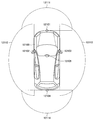
- FIG. 14 is an external view showing another example of an electronic device to which the solid-state imaging device according to the embodiment can be applied. It is a figure which shows an example of a schematic structure of an endoscopic surgery system. It is a block diagram which shows an example of a function structure of a camera head and CCU. It is a block diagram showing an example of rough composition of an internal information acquisition system. It is a block diagram showing an example of rough composition of a vehicle control system. It is explanatory drawing which shows an example of the installation position of a vehicle exterior information detection part and an imaging part.
- Solid-state imaging device 1.1. Schematic Configuration of Pixel Array 1.2. Specific configuration of pixel array Modified example 3. Application example 3.1. Electronic device 3.2. Endoscopic surgery system 3.3. Internal Information Acquisition System 3.4. Moving body
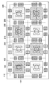
- FIG. 1 is a plan view showing an example of a planar layout of a pixel array provided in a solid-state imaging device according to the present embodiment.
- the planar layout of the pixel array 500 provided in the solid-state imaging device according to the present embodiment will be described.
- the pixel array 500 included in the solid-state imaging device according to the present embodiment is configured by arranging a plurality of pixels that respectively receive light of a predetermined wavelength band.
- the pixel array 500 is configured by arranging pixels (red pixels, green pixels and blue pixels) that respectively receive light in wavelength bands corresponding to red, green and blue in a predetermined array. It is also good.
- the pixel array 500 may be configured by repeatedly arranging pixel units in which four pixels of a red pixel, a blue pixel, and two green pixels form one set.
- the pixel array 500 may be configured by repeatedly arranging pixel units in which four pixels of red pixels, green pixels, blue pixels, and white pixels (that is, pixels without a color filter) are one set.
- the arrangement of the plurality of pixels in the pixel array 500 is not particularly limited. For example, various arrangements such as a delta arrangement, a stripe arrangement, a diagonal arrangement, or a rectangular arrangement can be applied.
- each of the pixels acquires distance measurement information for focus detection in addition to the pixel information for image generation.
- each of the pixels is configured by providing a pair of sub-pixels under one microlens in order to obtain distance measurement information for focus detection.
- a light flux incident from one side of the microlens is received by one sub-pixel, and a light flux incident from the other side of the microlens is received by the other sub-pixel.
- a shift amount (shift amount) that is correlated with the defocus amount of the focal point with respect to the subject is generated between the image received by one sub-pixel and the image received by the other sub-pixel.
- each of the pixels can detect the defocus amount of the focal point with respect to the subject by comparing the images received by each of the pair of sub-pixels with each other.
- the pixel array 500 includes the first pixel 100 in which the pair of sub pixels 110 and 120 are arranged in the first direction, and the pair of sub pixels 210 and 220. At least one or more second pixels 200 provided in line in a second direction orthogonal to one direction are included.
- the first pixel 100 includes a pair of sub pixels 110 and 120 and a pixel transistor group 150. Further, the second pixel 200 includes a pair of sub-pixels 210 and 220 and a pixel transistor group 250 similarly to the first pixel 100.
- the first pixel 100 and the second pixel 200 have substantially the same configuration except for the direction in which the pair of sub-pixels are arranged, and therefore, the first pixel 100 will be described below as an example.
- the pair of sub-pixels 110 and 120 are provided below the one microlens and the color filter in the first direction or the second direction, and ranging information for focus detection by photoelectrically converting incident light. And obtain pixel information for image generation.
- the sub pixels 110 and 120 can obtain information for focus detection by calculating the shift amount of the image received by each of the sub pixels 110 and 120.
- the sub-pixels 110 and 120 can acquire pixel information for obtaining a color image of a subject by performing signal processing on signals photoelectrically converted in each of the sub-pixels 110 and 120.
- the sub pixels 110 and 120 may be provided in the same planar shape. By providing the sub-pixels 110 and 120 with the same configuration except for the position with respect to the microlens, it is possible to accurately detect the amount of image shift due to pupil division. Specifically, the sub pixels 110 and 120 may be provided in the same planar shape so as to have the same aperture. For example, the planar shape of the sub pixels 110 and 120 may be a rectangular shape obtained by dividing a square into two.
- the pixel transistor group 150 generates information output from the first pixel 100 by transferring and amplifying signals output from the sub-pixels 110 and 120. Specifically, the pixel transistor group 150 may generate distance measurement information for focus detection and pixel information for image generation based on the signals output from the sub-pixels 110 and 120. For example, the pixel transistor group 150 may obtain pixel information for generating an image by adding up the signals output from each of the sub-pixels 110 and 120.
- each of the pixels of the pixel array 500 can obtain distance measurement information for focus detection and pixel information for image generation from the same pixel. Become.
- each of the pixels of the pixel array 500 acquires either information for focus detection or information for image generation, the more pixels for focus detection, the less pixels for acquiring pixel information. The image quality of the image is degraded. On the other hand, as the number of pixels for which focus detection is performed is reduced, the focusing accuracy is lowered, and the image tends to be blurred. That is, when each of the pixels of the pixel array 500 acquires either information for focus detection or information for image generation, the accuracy of focusing and the image quality of the image have a trade-off relationship. I will. On the other hand, according to the solid-state imaging device according to the present embodiment, it is possible to improve the focusing accuracy without degrading the image quality of the image.
- the directions in which the pair of sub-pixels are arranged are orthogonal to each other.
- the amount of shift in focus with respect to the object is calculated using the amount of shift generated between the image received by one sub-pixel and the image received by the other sub-pixel doing. Therefore, it may be difficult to detect an accurate defocus amount for an object having a shape that does not easily generate a displacement amount between each of the pair of sub-pixels. For example, in the case where the subject has an elongated shape extending in a direction orthogonal to the direction in which the pair of sub-pixels is arranged, an accurate defocus amount is detected only with the pixel in which the pair of sub-pixels is arranged in one direction. Can be difficult.
- the shape of the object is elongated in any direction Even with the shape, it is possible to detect an accurate defocus amount.
- the pixel array 500 even if the shape of the subject is elongated in any direction, an accurate defocus amount is detected in either the first pixel 100 or the second pixel 200. Is possible. Therefore, according to the solid-state imaging device according to the present embodiment, it is possible to perform focus detection and image generation on subjects of various shapes, and thus it is possible to obtain a clearer image.
- the planar shape of the first pixel 100 and the second pixel 200 may be a four-fold symmetric planar shape.
- the planar shapes of the first pixel 100 and the second pixel 200 may be shapes that coincide with each other by rotating 90 ° around the center of gravity.
- the planar shape of the first pixel 100 and the second pixel 200 is four-fold symmetric, the second pixel 200 can be formed by rotating the first pixel 100 by 90 °.
- the two pixels 200 can be more easily mixed and formed.
- a four-fold symmetrical shape for example, a square, regular octagon or circular shape can be exemplified.
- the first pixel 100 and the second pixel 200 may have the same planar shape. In such a case, it is easy to spread the first pixel 100 and the second pixel 200 in the pixel array 500. Further, in such a case, since the aperture ratio of the pixel is the same in each of the first pixel 100 and the second pixel 200, it may be used for image generation without correcting the pixel information acquired from each pixel. it can.
- the pixel array 500 may include pixels having at least one or more pairs of sub-pixels for obtaining distance measurement information for focusing as described above and pixel information for image generation. That is, the pixel array 500 may include at least one or more of the first pixel 100 and the second pixel 200 described above. In such a case, the green pixel may be the first pixel 100 and the second pixel 200 including a pair of sub-pixels.
- the green light photoelectrically converted by the green pixel is more easily absorbed by the silicon photodiode than the red light and blue light photoelectrically converted by the red pixel and the blue pixel, so it is easily photoelectrically converted and a signal is easily obtained. Therefore, when the first pixel 100 and the second pixel 200 are green pixels, it is possible to obtain distance measurement information for focus detection with higher accuracy.
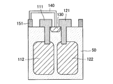
- FIG. 2 is a longitudinal sectional view showing the configuration of one sub-pixel in FIG.
- the sub-pixels constituting the first pixel 100 and the second pixel 200 and the like are configured by the photoelectric conversion element 11 embedded in the semiconductor substrate 50, the transfer transistor 12, and the floating diffusion layer 13. Be done.
- the pixel control transistor 14 is, for example, one of the transistors included in the transistor group shown as the pixel transistor group 150 in FIG.
- the semiconductor substrate 50 is a substrate formed of a semiconductor material.
- the semiconductor substrate 50 may be a silicon substrate.
- the semiconductor substrate 50 is a substrate formed of another elemental semiconductor such as germanium or a substrate formed of a compound semiconductor such as gallium arsenide (GaAs), gallium nitride (GaN) or silicon carbide (SiC). It is also good.
- GaAs gallium arsenide
- GaN gallium nitride
- SiC silicon carbide
- the photoelectric conversion element 11 is, for example, a photodiode, and is embedded in the semiconductor substrate 50 and provided. Specifically, the photoelectric conversion element 11 converts light incident on the sub-pixel into electrons and holes by the photovoltaic effect by the pn junction or the pin junction.
- the photoelectric conversion element 11 may be configured by an n-type semiconductor region provided inside a p-type semiconductor region. In the photoelectric conversion element 11, when light is incident, electrons are generated in the n-type semiconductor region, and holes are generated in the p-type semiconductor region.
- the sub-pixel can convert the light incident on the sub-pixel into a signal by extracting the electrons generated in the n-type semiconductor region by the transfer transistor 12.
- the transfer transistor 12 takes out the charge from the photoelectric conversion element 11 provided inside the semiconductor substrate 50 and transfers the taken out charge to the floating diffusion layer 13 on the surface of the semiconductor substrate 50.
- the transfer transistor 12 is provided as a vertical transistor having a vertical gate structure extending toward the inside of the semiconductor substrate 50, and causes the photoelectric conversion element 11 and the floating diffusion layer 13 to function as a source or drain region. . Therefore, when a voltage higher than the threshold voltage is applied to the vertical gate, the transfer transistor 12 forms a channel along the vertical gate, thereby floating the charge generated in the photoelectric conversion element 11 into the floating diffusion layer 13. Can be transferred to
- the floating diffusion layer 13 is formed as an n-type semiconductor region and stores charge.
- the floating diffusion layer 13 functions as a floating diffusion.
- the floating diffusion layer 13 controls, for example, the gate voltage of the amplification transistor by the potential generated by the accumulated charge, and reads out the signal generated by the light reception of the sub-pixel to the outside of the pixel.
- the pixel control transistor 14 is a field effect transistor provided on the surface of the semiconductor substrate 50.
- the pixel control transistor 14 includes a gate electrode provided on the semiconductor substrate 50 and a source or drain region provided on the semiconductor substrate 50 with the gate electrode interposed therebetween.
- the pixel control transistor 14 may be provided in a region overlapping with the photoelectric conversion element 11 when the main surface of the semiconductor substrate 50 is viewed in plan.
- the photoelectric conversion element 11 is embedded in the semiconductor substrate 50, and the distance from the surface of the semiconductor substrate 50 is large. According to this configuration, it is possible to superimpose the pixel control transistor 14 that is easily affected by noise or the like on the photoelectric conversion element 11 when the pixel control transistor 11 approaches the photoelectric conversion element 11.
- the photoelectric conversion element 11 and the pixel control transistor 14 can be formed so as to be superimposed on the same planar region, so that the volume of the photoelectric conversion element 11 can be increased.
- the sub-pixel can reduce the area of the entire sub-pixel without reducing the sensitivity, the amount of saturated electrons, and the like of the photoelectric conversion element 11.
- FIG. 3A is a plan view showing a plan configuration of one pixel of the solid-state imaging device according to the present embodiment
- FIG. 3B is a longitudinal sectional view schematically showing a cross section cut along line A-AA in FIG. 3A.
- FIG. 3C is a circuit diagram showing an equivalent circuit of the configuration shown in FIG. 3A.
- the first pixel 100 is described as an example, the second pixel 200 is the same except that the arrangement direction of the pair of sub-pixels is different.
- the first pixel 100 includes a pair of sub-pixels 110 and 120, vertical gate electrodes 111 and 121, a floating diffusion layer 130, a pixel wiring 140, and an amplification transistor 151.
- a selection transistor 152, a reset transistor 153, and a dummy gate 154 are provided.
- photoelectric conversion elements 112 and 122 are provided in the semiconductor substrate 50 in the regions corresponding to the sub-pixels 110 and 120, respectively.
- the pair of sub pixels 110 and 120 includes a pair of photoelectric conversion elements 112 and 122 formed inside the semiconductor substrate 50, and converts the received light into a charge.
- the pair of sub-pixels 110 and 120 correspond to a pair of photoelectric conversion elements 112 and 122
- the photoelectric conversion elements 112 and 122 are a pair of n-type semiconductor regions provided inside a p-type semiconductor region. It consists of In the photoelectric conversion elements 112 and 122, the incident light is converted into charges by the photovoltaic effect. Specifically, electrons are generated in the n-type semiconductor region, and holes are generated in the p-type semiconductor region.
- the photoelectric conversion elements 112 and 122 can convert the amount of incident light into the amount of electrons generated in the n-type semiconductor region. Note that since the photoelectric conversion elements 112 and 122 are p-type semiconductor regions between n-type semiconductor regions, they are electrically separated from each other by potential barriers.
- the photoelectric conversion elements 112 and 122 can be increased in volume by being provided inside the semiconductor substrate 50, so that the sensitivity, the amount of saturated electrons, and the like can be increased without increasing the planar occupied area. it can.
- the semiconductor substrate 50 may be a substrate formed of a semiconductor material such as silicon, a substrate formed of another elemental semiconductor such as germanium, or gallium arsenide (GaAs), gallium nitride (GaN), or silicon carbide It may be a substrate formed of a compound semiconductor such as SiC).
- the vertical gate electrodes 111 and 121 are gates of field effect transistors that transfer the charges generated by the photoelectric conversion elements 112 and 122 to the floating diffusion layer 130, respectively.
- the vertical gate electrodes 111 and 121 are provided in the form of vertically elongated columns extending inside the semiconductor substrate 50 in order to extract charges from the photoelectric conversion elements 112 and 122 provided inside the semiconductor substrate 50.
- the vertical gate electrodes 111 and 121 form a channel between the photoelectric conversion elements 112 and 122 and the floating diffusion layer 130 along the vertical gate electrodes 111 and 121, respectively using the source and drain regions.
- the vertical gate electrodes 111 and 121 can transfer charges from the photoelectric conversion elements 112 and 122 to the floating diffusion layer 130 through the formed channel.
- the floating diffusion layer 130 is formed as an n-type semiconductor region, and stores charge.
- the floating diffusion layer 130 functions as a floating diffusion.
- the charge transferred from the photoelectric conversion elements 112 and 122 and accumulated in the floating diffusion layer 130 generates a potential to control the gate voltage of the amplification transistor 151 via the pixel wiring 140.
- the floating diffusion layer 130 may be provided, for example, at the boundary between the pair of sub-pixels 110 and 120 (that is, the photoelectric conversion elements 112 and 122). More specifically, the floating diffusion layer 130 may be provided at the center of the first pixel 100 configured by the pair of sub-pixels 110 and 120. In such a case, the center of the floating diffusion layer 130 can be substantially aligned with the center of the microlens provided on the first pixel 100.
- the pixel wiring 140 is a wiring and a contact which electrically connect the floating diffusion layer 130 and the gate electrode of the amplification transistor 151 and electrically connect the floating diffusion layer 130 and the source or drain region of the reset transistor 153.
- the pixel line 140 may be formed of a metal such as copper (Cu), aluminum (Al), titanium (Ti), or tungsten (W).
- the pixel wiring 140 may be formed of one type of metal or may be formed of a plurality of types of metals. For example, the pixel wiring 140 may be formed of a different metal for each wiring and contact.
- the gate electrode of the amplification transistor 151 is electrically connected to the floating diffusion layer 130 by the pixel wiring 140, and on / off is controlled by the potential generated by the charge accumulated in the floating diffusion layer 130. Specifically, when the potential generated by the charge accumulated in the floating diffusion layer 130 exceeds the threshold, the amplification transistor 151 is turned on to cause a current to flow between the source and the drain. Thereby, the amplification transistor 151 can convert and amplify the charge stored in the floating diffusion layer 130 into the current between the source and the drain.
- the selection transistor 152 is connected in series to the amplification transistor 151, and controls selection or non-selection of a pixel. Specifically, the selection transistor 152 controls whether or not the signal is read from the first pixel 100 by the voltage applied to the gate electrode. Thereby, in the solid-state imaging device, signals can be read out sequentially from each of the pixels.
- the source or drain region and the floating diffusion layer 130 are electrically connected by the pixel wiring 140, and the potential of the floating diffusion layer 130 is controlled.
- the source or drain of the reset transistor 153 is connected to, for example, a power supply (VDD).
- the reset transistor 153 is turned on to form a channel between the source and the drain, and controls the potential of the floating diffusion layer 130 to be equal to the potential of the power supply (VDD).
- the dummy gate 154 is an electrode which is not electrically connected to the wiring for exchanging signals and the like but is electrically connected to the ground. That is, the dummy gate 154 is an electrode that is not used for signal processing of the signal output from the first pixel 100.
- the dummy gate 154 is provided to make the arrangement of gate electrodes provided around the pair of sub-pixels 110 and 120 of the first pixel 100 symmetrical with respect to the sub-pixels 110 and 120.
- the dummy gate 154 is provided so that light reflected by each gate electrode of the amplification transistor 151, the selection transistor 152, and the reset transistor 153 leaks symmetrically to the photoelectric conversion elements 112 and 122.
- the amplification transistor 151, the selection transistor 152, the reset transistor 153, and the dummy gate 154 are formed along two sides of the first pixel 100 configured by a pair of sub pixels 110 and 120. On the remaining two sides of the first pixel 100, any of the amplification transistor 151, the selection transistor 152, the reset transistor 153, and the dummy gate 154 of the adjacent pixel may be formed.
- FIG. 3C An equivalent circuit of the circuit of the first pixel 100 described above is shown in FIG. 3C.
- the photoelectric conversion elements 112 and 122 are connected to the gate of the amplification transistor 151 via the floating diffusion layer 130.
- the floating diffusion layer 130 is connected to the power supply (VDD) through the source or drain of the reset transistor 153.
- the amplification transistor 151 is connected in series to the selection transistor 152, the source or drain of the amplification transistor 151 is connected to the power supply (VDD), and the source or drain of the selection transistor 152 is connected to the output (VOUT).
- the charge photoelectrically converted by the photoelectric conversion elements 112 and 122 is output to the floating diffusion layer 130 by the potential difference between the ground and the VDD.
- the output charge is accumulated in the floating diffusion layer 130 to increase the voltage applied to the gate of the amplification transistor 151, thereby turning on the amplification transistor 151.
- the selection transistor 152 is turned on to form an electrical connection from the power supply (VDD) to the output (VOUT).
- VDD power supply
- VOUT output
- the reset transistor 153 is turned on to discharge the charge stored in the floating diffusion layer 130, and the potential of the floating diffusion layer 130 is reset to the potential of the power supply (VDD). It is set. Thus, the floating diffusion layer 130 returns to the state before the charge photoelectrically converted by the photoelectric conversion elements 112 and 122 is accumulated.
- FIG. 3D is a plan view showing a planar configuration of the wiring for each of the first pixel 100 and the second pixel 200.
- FIG. 3D shows a specific example of the wiring connection in the case where the first pixel 100 and the second pixel 200 are adjacent to each other.
- the second pixel 200 has substantially the same configuration as the first pixel 100 except that the arrangement direction of the pair of sub-pixels 210 and 220 is different.
- the second pixel 200 includes a pair of sub-pixels 210 and 220, vertical gate electrodes 211 and 221, a floating diffusion layer 230, a pixel wiring 240, an amplification transistor 251, and a selection transistor 252, A reset transistor 253 and a dummy gate 254 are provided. These configurations are substantially the same as the configurations of the same name described in the first pixel 100.
- the pixel wiring 140 is provided in a shape bent in a bowl shape.
- the pixel wiring 140 is electrically connected to the floating diffusion layer 130 by the contact 163 provided at the apex of the wedge shape, and electrically connected to the gate electrode of the amplification transistor 151 by the contact 162 provided at one end of the wedge shape.
- the pixel wiring 240 is provided in a wedge shape.
- the pixel wiring 240 is electrically connected to the floating diffusion layer 230 at the contact 263 provided at the apex of the wedge, and electrically connected to the gate electrode of the amplification transistor 251 at the contact 262 provided at one end of the wedge. Connecting.
- gate wirings 141 and 142 for controlling on / off of transfer transistors that control transfer of charges from each of the pair of sub-pixels 110 and 120 are provided in the form of parallel line segments.
- the gate wiring 141 is electrically connected to the vertical gate electrode 111 at the contact 161
- the gate wiring 142 is electrically connected to the vertical gate electrode 121 at the contact 164.
- the contact 161 and the contact 164 are provided to be located on the diagonal of the first pixel 100, respectively. Since the gate wirings 141 and 142 are provided in the same layer as the pixel wiring 140, they are provided so as not to overlap with each other.
- the pixel wiring 140 is provided on the third quadrant side of the first pixel 100
- the gate wiring 141 is provided on the first quadrant and the second quadrant side
- the gate wiring 142 is provided on the fourth quadrant side.
- the gate wirings 141 and 142 are electrically connected to the interpixel wirings 310 and 320 provided in the upper layer by the vias 171 and 172, respectively.
- gate wirings 241 and 242 for controlling on / off of transfer transistors for controlling transfer of charges from each of the pair of sub-pixels 210 and 220 are provided in the form of parallel line segments.
- the gate wiring 241 is electrically connected to the vertical gate electrode 211 at the contact 261
- the gate wiring 242 is electrically connected to the vertical gate electrode 221 at the contact 264.
- the contact 261 and the contact 264 are provided on the diagonal of the second pixel 200, respectively. Since the gate wirings 241 and 242 are provided in the same layer as the pixel wiring 240, they are provided so as not to overlap with each other.
- the pixel wiring 240 is provided on the third quadrant side of the second pixel 200
- the gate wiring 241 is provided on the first quadrant and the second quadrant side
- the gate wiring 242 is provided on the fourth quadrant side.
- the gate wirings 241 and 242 are electrically connected to the interpixel wirings 310 and 320 provided in the upper layer by the vias 271 and 272, respectively.
- the arrangement direction of the pair of sub-pixels is orthogonal.
- the first pixel 100 and the second pixel 200 have the same wiring shape by providing contacts for the vertical gate electrodes provided in each of the pair of sub-pixels on the diagonal of each pixel. Can be connected.
- the pixel wiring 140 and the gate wirings 141 and 142, and the pixel wiring 240 and the gate wirings 241 and 242 can be provided in the same shape.
- the inter-pixel wirings 310 and 320 provided over the first pixel 100 and the second pixel 200 can be provided in a linear shape extending in one direction.
- the first pixel 100 and the second pixel 200 are provided with the wiring of the same shape, there is no difference in the conversion efficiency with respect to the parasitic capacitance. Further, even when the arrangement of the first pixel 100 and the second pixel 200 is changed, it is possible to cope with the case without changing the wiring only by changing the configuration of the transistor of the semiconductor substrate 50.
- FIG. 4 is a longitudinal sectional view showing a modification of the configuration of one sub-pixel.
- the sub-pixels constituting the first pixel 100, the second pixel 200, etc. are formed of the photoelectric conversion element 11 embedded in the semiconductor substrate 50, the extraction region 16, the transfer transistor 15, and the floating diffusion layer. 13 and the pixel control transistor 14.
- the transfer transistor 15 does not have a vertical gate structure, but has a planar gate structure in which a gate is provided on the surface of a semiconductor substrate 50.
- a lead-out area 16 extending from the photoelectric conversion element 11 toward the surface of the semiconductor substrate 50 is provided.
- description here is abbreviate
- the lead-out area 16 is an n-type semiconductor area, and the electrons generated in the n-type semiconductor area of the photoelectric conversion element 11 are drawn to the surface of the semiconductor substrate 50.
- the transfer transistor 15 can function as a gate the electrode provided on the surface of the semiconductor substrate 50, and can function the extraction region 16 and the floating diffusion layer 13 as a source or drain region. That is, in the transfer transistor 15, when a voltage higher than the threshold voltage is applied to the gate electrode provided on the surface of the semiconductor substrate 50, the channel between the floating region 13 and the extraction region 16 near the surface of the semiconductor substrate 50. Can be formed.
- the transfer transistor 15 can transfer the electrons generated by the photoelectric conversion element 11 to the floating diffusion layer 13 through the lead-out region 16.
- FIG. 5A is a plan view showing a modification of a planar configuration including a plurality of pixels
- FIG. 5B is a circuit diagram showing an equivalent circuit of the configuration shown in FIG. 5A.
- the floating diffusion layers 131 and 132 of two pixels are electrically connected by the pixel wiring 140, so that the pixel transistor group 150 after the amplification transistor is shared by two pixels. doing.
- the floating diffusion layer 131 which accumulates the charge photoelectrically converted in the pair of sub-pixels 110A and 120A of the first pixel 101, and the pair of sub-pixels 110B and 120B of the first pixel 102.
- the pixel wiring 140 electrically connects to the floating diffusion layer 132 which stores the photoelectrically converted charge.
- the floating diffusion layer 131, the floating diffusion layer 132, and the pixel wiring 140 are at the same potential, so that the entire floating diffusion layer 131, the floating diffusion layer 132, and the pixel wiring 140 can function as one floating diffusion.
- the first pixels 101 and 102 can share the pixel transistor group 150 (that is, the amplification transistor, the selection transistor, and the reset transistor) constituting the circuit of the latter stage of the floating diffusion by two pixels,
- the area occupied by the signal processing circuit can be reduced, and the area occupied by the pixel can be expanded.
- the photoelectric conversion is performed by the floating diffusion layer 133 that accumulates the charge photoelectrically converted by the pair of sub-pixels 110C and 120C of the first pixel 103 and the pair of sub-pixels 210 and 220 of the second pixel 201
- the pixel wiring 240 electrically connects the floating diffusion layer 230 for storing the charge.
- the floating diffusion layer 133, the floating diffusion layer 230, and the pixel wiring 240 are at the same potential, so that the entire floating diffusion layer 133, the floating diffusion layer 230, and the pixel wiring 140 can function as one floating diffusion.
- the first pixel 103 and the second pixel 201 can share the pixel transistor group 250 (that is, the amplification transistor, the selection transistor, and the reset transistor) constituting the circuit of the latter stage of the floating diffusion by two pixels. Therefore, the area occupied by the signal processing circuit can be reduced, and the area occupied by the pixel can be expanded.
- the pixel transistor group 250 that is, the amplification transistor, the selection transistor, and the reset transistor
- FIG. 5B An equivalent circuit of the circuit of the first pixels 101 and 102 sharing the signal processing circuit described in FIG. 5A is shown in FIG. 5B.
- the floating diffusion layers 131 and 132 and the pixel wiring 140 function as floating diffusions and are connected to the gate of the amplification transistor 151.
- the floating diffusion is connected to the power supply (VDD) through the source or drain of the reset transistor 153.
- the amplification transistor 151 is connected in series to the selection transistor 152, the source or drain of the amplification transistor 151 is connected to the power supply (VDD), and the source or drain of the selection transistor 152 is connected to the output (VOUT) There is.
- the charges photoelectrically converted in each of the sub-pixels 110A, 120A, 110B, and 120B are output to the floating diffusion layers 131 and 132 by the potential difference between the ground and the VDD.
- the output charge is accumulated across the floating diffusion layers 131 and 132 and the pixel wiring 140 to increase the voltage applied to the gate of the amplification transistor 151, thereby turning on the amplification transistor 151.
- the selection transistor 152 is turned on to form an electrical connection from the power supply (VDD) to the output (VOUT).
- VDD power supply
- VOUT output
- the reset transistor 153 is turned on, whereby the charges accumulated over the floating diffusion layers 131 and 132 and the pixel wiring 140 are discharged, and the potential of the floating diffusion layers 131 and 132 Is reset to the potential of the power supply (VDD). Thereby, the floating diffusion layers 131 and 132 return to the state before the charge is accumulated.
- FIG. 6 is a plan view showing a modification of the plane configuration including a plurality of pixels.
- the floating diffusion layer 130 is provided at the boundary between two pixels, so that the pixel transistor group 150 constituting the circuit of the subsequent stage of the floating diffusion layer 130 is shared by two pixels. ing.
- the charge photoelectrically converted in the pair of sub-pixels 110A and 120A of the first pixel 101 and the charge photoelectrically converted in the pair of sub-pixels 110B and 120B of the first pixel 102 are the first It is accumulated in the floating diffusion layer 130 provided at the boundary between the pixels 101 and 102.
- the floating diffusion layer 130 is electrically connected to the pixel transistor group 150 including the amplification transistor and the reset transistor by the pixel wiring 140. According to this, since the first pixels 101 and 102 can share the floating diffusion layer 130 and the pixel transistor group 150 (that is, the amplification transistor, the selection transistor, and the reset transistor) by two pixels, the signal processing circuit The area occupied can be reduced, and the area occupied by the pixel can be enlarged.
- the charge photoelectrically converted by the pair of sub-pixels 210A and 220A of the second pixel 201 and the charge photoelectrically converted by the pair of sub-pixels 210B and 220B of the second pixel 202 are the second It is accumulated in the floating diffusion layer 230 provided at the boundary between the pixels 201 and 202.
- the floating diffusion layer 230 is electrically connected to the pixel transistor group 250 including the amplification transistor and the reset transistor by the pixel wiring 240.
- the second pixels 201 and 202 can share the floating diffusion layer 230 and the pixel transistor group 250 (that is, the amplification transistor, the selection transistor, and the reset transistor) by two pixels, the signal processing circuit The area occupied can be reduced, and the area occupied by the pixel can be enlarged.
- FIG. 7 is a plan view showing a modification of the plane configuration of the pixel array 500. As shown in FIG.
- the pixel array 500 may be provided to be inclined with respect to the solid-state imaging device. Specifically, the pixel array 500 may be provided to be inclined 45 ° with respect to the horizontal direction of the solid-state imaging device.
- the pair of sub-pixels 110 and 120 of the first pixel 100 are arranged in a direction inclined 45 ° clockwise, for example, with respect to the horizontal direction of the solid-state imaging device.
- the pair of sub-pixels 110 and 120 of the second pixel 200 are arranged in a direction inclined 45 ° counterclockwise, for example, with respect to the horizontal direction of the solid-state imaging device.
- the pixel array 500 provided in the solid-state imaging device according to the present embodiment may have another planar configuration other than the planar configuration in which each of the pixels is arranged in a matrix.
- FIG. 8 is a plan view showing a modification of the planar configuration of the pixel array 500. As shown in FIG.
- the pixel array 500 may be provided at an angle to the solid-state imaging device. Specifically, the pixel array 500 may be provided to be inclined 45 ° with respect to the horizontal direction of the solid-state imaging device.
- the pair of sub-pixels 110 and 120 of the first pixel 100 are provided to be arranged in the vertical direction with respect to the horizontal direction of the solid-state imaging device.
- the sub-pixels 110 and 120 are arranged in the horizontal direction of the solid-state imaging device.
- the planar shape of the pair of sub-pixels of each pixel may be, for example, a right-angled isosceles triangle obtained by cutting a square with a diagonal.
- the shape of the pair of sub-pixels may be another shape other than a rectangle obtained by equally dividing a square into two.
- the first to fifth modifications described above can be combined with one another as long as no contradiction arises, and these are also included in the technical scope of the present disclosure.
- a plurality of types of plane configurations according to the second to fifth modifications may be included in the same pixel array 500.
- the solid-state imaging device according to an embodiment of the present disclosure can be applied to, for example, an imaging unit mounted in various electronic devices. Subsequently, examples of electronic devices to which the solid-state imaging device according to the present embodiment can be applied will be described with reference to FIGS. 9A to 9C.
- 9A to 9C are external views showing an example of an electronic apparatus to which the solid-state imaging device according to the present embodiment can be applied.
- the solid-state imaging device according to the present embodiment can be applied to an imaging unit mounted in an electronic device such as a smartphone.
- the smartphone 900 includes a display unit 901 for displaying various information, and an operation unit 903 configured of a button or the like for receiving an operation input by the user.
- the solid-state imaging device according to the present embodiment may be applied to the imaging unit included in the smartphone 900.
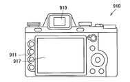
- the solid-state imaging device can be applied to an imaging unit mounted in an electronic device such as a digital camera.
- the digital camera 910 includes a main body (camera body) 911, an interchangeable lens unit 913, a grip 915 gripped by the user at the time of photographing, A monitor unit 917 for displaying information and an EVF (Electronic View Finder) 919 for displaying a through image observed by the user at the time of shooting are provided.
- 9B is an external view of the digital camera 910 as viewed from the front (ie, the object side)
- FIG. 9C is an external view of the digital camera 910 as viewed from the rear (ie, the photographer side).
- the solid-state imaging device may be applied to the imaging unit of the digital camera 910.
- the electronic device to which the solid-state imaging device according to the present embodiment is applied is not limited to the above example.
- the solid-state imaging device according to the present embodiment can be applied to an imaging unit mounted in an electronic device in any field.
- an electronic device for example, a glasses-type wearable device, an HMD (Head Mounted Display), a television device, an electronic book, a PDA (Personal Digital Assistant), a notebook personal computer, a video camera, a game device, etc. are illustrated. be able to.
- FIG. 10 is a diagram showing an example of a schematic configuration of an endoscopic surgery system to which the technology (the present technology) according to the present disclosure can be applied.
- FIG. 10 illustrates how a surgeon (doctor) 11131 is performing surgery on a patient 11132 on a patient bed 11133 using the endoscopic surgery system 11000.
- the endoscopic surgery system 11000 includes an endoscope 11100, other surgical instruments 11110 such as an insufflation tube 11111 and an energy treatment instrument 11112, and a support arm device 11120 for supporting the endoscope 11100.
- a cart 11200 on which various devices for endoscopic surgery are mounted.
- the endoscope 11100 includes a lens barrel 11101 whose region of a predetermined length from the tip is inserted into a body cavity of a patient 11132, and a camera head 11102 connected to a proximal end of the lens barrel 11101.
- the endoscope 11100 configured as a so-called rigid endoscope having a rigid barrel 11101 is illustrated, but even if the endoscope 11100 is configured as a so-called flexible mirror having a flexible barrel Good.
- the endoscope 11100 may be a straight endoscope, or may be a oblique endoscope or a side endoscope.
- An optical system and an imaging device are provided inside the camera head 11102, and the reflected light (observation light) from the observation target is condensed on the imaging device by the optical system.
- the observation light is photoelectrically converted by the imaging element to generate an electric signal corresponding to the observation light, that is, an image signal corresponding to the observation image.
- the image signal is transmitted as RAW data to a camera control unit (CCU: Camera Control Unit) 11201.
- CCU Camera Control Unit
- the CCU 11201 is a CPU (Central Processing Unit) or a GPU (Graphics). (Processing Unit) etc., and controls the operation of the endoscope 11100 and the display device 11202 in a centralized manner. Furthermore, the CCU 11201 receives an image signal from the camera head 11102 and performs various image processing for displaying an image based on the image signal, such as development processing (demosaicing processing), on the image signal.
- image processing demosaicing processing
- the display device 11202 displays an image based on an image signal subjected to image processing by the CCU 11201 under control of the CCU 11201.
- the light source device 11203 includes, for example, a light source such as an LED (light emitting diode), and supplies the endoscope 11100 with irradiation light at the time of imaging an operation part or the like.
- a light source such as an LED (light emitting diode)
- the input device 11204 is an input interface to the endoscopic surgery system 11000.
- the user can input various information and input instructions to the endoscopic surgery system 11000 via the input device 11204.
- the user inputs an instruction to change the imaging condition (type of irradiated light, magnification, focal length, and the like) by the endoscope 11100, and the like.
- the treatment tool control device 11205 controls the drive of the energy treatment tool 11112 for ablation of tissue, incision, sealing of a blood vessel, and the like.
- the insufflation apparatus 11206 is a gas within the body cavity via the insufflation tube 11111 in order to expand the body cavity of the patient 11132 for the purpose of securing a visual field by the endoscope 11100 and securing a working space of the operator.
- Send The recorder 11207 is a device capable of recording various types of information regarding surgery.
- the printer 11208 is an apparatus capable of printing various types of information regarding surgery in various types such as text, images, and graphs.
- the light source device 11203 that supplies the irradiation light when imaging the surgical site to the endoscope 11100 can be configured of, for example, an LED, a laser light source, or a white light source configured by a combination of these.
- a white light source is configured by a combination of RGB laser light sources
- the output intensity and output timing of each color (each wavelength) can be controlled with high precision. It can be carried out.
- the laser light from each of the RGB laser light sources is irradiated to the observation target in time division, and the drive of the image pickup element of the camera head 11102 is controlled in synchronization with the irradiation timing to cope with each of RGB. It is also possible to capture a shot image in time division. According to the method, a color image can be obtained without providing a color filter in the imaging device.
- the drive of the light source device 11203 may be controlled so as to change the intensity of the light to be output every predetermined time.
- the drive of the imaging device of the camera head 11102 is controlled in synchronization with the timing of the change of the light intensity to acquire images in time division, and by combining the images, high dynamic without so-called blackout and whiteout is obtained. An image of the range can be generated.
- the light source device 11203 may be configured to be able to supply light of a predetermined wavelength band corresponding to special light observation.
- special light observation for example, the mucous membrane surface layer is irradiated by irradiating narrow band light as compared with irradiation light (that is, white light) at the time of normal observation using the wavelength dependency of light absorption in body tissue.
- the so-called narrow band imaging is performed to image a predetermined tissue such as a blood vessel with high contrast.
- fluorescence observation may be performed in which an image is obtained by fluorescence generated by irradiation with excitation light.
- body tissue is irradiated with excitation light and fluorescence from the body tissue is observed (autofluorescence observation), or a reagent such as indocyanine green (ICG) is locally injected into body tissue and the body tissue is Excitation light corresponding to the fluorescence wavelength of the reagent can be irradiated to obtain a fluorescence image or the like.
- the light source device 11203 can be configured to be able to supply narrow band light and / or excitation light corresponding to such special light observation.
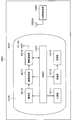
- FIG. 11 is a block diagram showing an example of functional configurations of the camera head 11102 and the CCU 11201 shown in FIG.
- the camera head 11102 includes a lens unit 11401, an imaging unit 11402, a drive unit 11403, a communication unit 11404, and a camera head control unit 11405.
- the CCU 11201 includes a communication unit 11411, an image processing unit 11412, and a control unit 11413.
- the camera head 11102 and the CCU 11201 are communicably connected to each other by a transmission cable 11400.
- the lens unit 11401 is an optical system provided at a connection portion with the lens barrel 11101.
- the observation light taken in from the tip of the lens barrel 11101 is guided to the camera head 11102 and is incident on the lens unit 11401.
- the lens unit 11401 is configured by combining a plurality of lenses including a zoom lens and a focus lens.
- the imaging device constituting the imaging unit 11402 may be one (a so-called single-plate type) or a plurality (a so-called multi-plate type).
- the imaging unit 11402 When the imaging unit 11402 is configured as a multi-plate type, for example, an image signal corresponding to each of RGB may be generated by each imaging element, and a color image may be obtained by combining them.
- the imaging unit 11402 may be configured to have a pair of imaging devices for acquiring image signals for right eye and left eye corresponding to 3D (dimensional) display. By performing 3D display, the operator 11131 can more accurately grasp the depth of the living tissue in the operation site.
- a plurality of lens units 11401 may be provided corresponding to each imaging element.
- the imaging unit 11402 may not necessarily be provided in the camera head 11102.
- the imaging unit 11402 may be provided inside the lens barrel 11101 immediately after the objective lens.
- the driving unit 11403 is configured by an actuator, and moves the zoom lens and the focusing lens of the lens unit 11401 by a predetermined distance along the optical axis under the control of the camera head control unit 11405. Thereby, the magnification and the focus of the captured image by the imaging unit 11402 can be appropriately adjusted.
- the communication unit 11404 is configured of a communication device for transmitting and receiving various types of information to and from the CCU 11201.
- the communication unit 11404 transmits the image signal obtained from the imaging unit 11402 to the CCU 11201 as RAW data via the transmission cable 11400.
- the communication unit 11404 also receives a control signal for controlling the drive of the camera head 11102 from the CCU 11201 and supplies the control signal to the camera head control unit 11405.
- the control signal includes, for example, information indicating that the frame rate of the captured image is designated, information indicating that the exposure value at the time of imaging is designated, and / or information indicating that the magnification and focus of the captured image are designated, etc. Contains information about the condition.
- the imaging conditions such as the frame rate, exposure value, magnification, and focus described above may be appropriately designated by the user, or may be automatically set by the control unit 11413 of the CCU 11201 based on the acquired image signal. Good. In the latter case, the so-called AE (Auto Exposure) function, AF (Auto Focus) function, and AWB (Auto White Balance) function are incorporated in the endoscope 11100.
- AE Auto Exposure
- AF Auto Focus
- AWB Automatic White Balance
- the camera head control unit 11405 controls the drive of the camera head 11102 based on the control signal from the CCU 11201 received via the communication unit 11404.
- the communication unit 11411 is configured by a communication device for transmitting and receiving various types of information to and from the camera head 11102.
- the communication unit 11411 receives an image signal transmitted from the camera head 11102 via the transmission cable 11400.
- the communication unit 11411 transmits a control signal for controlling driving of the camera head 11102 to the camera head 11102.
- the image signal and the control signal can be transmitted by telecommunication or optical communication.
- An image processing unit 11412 performs various types of image processing on an image signal that is RAW data transmitted from the camera head 11102.
- the control unit 11413 performs various types of control regarding imaging of a surgical site and the like by the endoscope 11100 and display of a captured image obtained by imaging of the surgical site and the like. For example, the control unit 11413 generates a control signal for controlling the drive of the camera head 11102.
- control unit 11413 causes the display device 11202 to display a captured image in which a surgical site or the like is captured, based on the image signal subjected to the image processing by the image processing unit 11412.
- the control unit 11413 may recognize various objects in the captured image using various image recognition techniques. For example, the control unit 11413 detects a shape, a color, and the like of an edge of an object included in a captured image, thereby enabling a surgical tool such as forceps, a specific biological site, bleeding, mist when using the energy treatment tool 11112, and the like. It can be recognized.
- control unit 11413 may superimpose various surgical support information on the image of the surgery section using the recognition result.
- the operation support information is superimposed and presented to the operator 11131, whereby the burden on the operator 11131 can be reduced and the operator 11131 can reliably proceed with the operation.
- a transmission cable 11400 connecting the camera head 11102 and the CCU 11201 is an electric signal cable corresponding to communication of an electric signal, an optical fiber corresponding to optical communication, or a composite cable of these.
- communication is performed by wire communication using the transmission cable 11400, but communication between the camera head 11102 and the CCU 11201 may be performed wirelessly.
- the technology according to the present disclosure may be applied to, for example, the endoscope 11100 or the camera head 11102 among the configurations described above.
- the solid-state imaging device according to the present embodiment can be applied to the endoscope 11100 or the imaging unit 11402 of the camera head 11102.
- the technology according to the present disclosure may be applied to an in-vivo information acquisition system.
- FIG. 12 is a block diagram showing an example of a schematic configuration of a patient's in-vivo information acquiring system using a capsule endoscope to which the technology (the present technology) according to the present disclosure can be applied.
- the in-vivo information acquisition system 10001 includes a capsule endoscope 10100 and an external control device 10200.
- the capsule endoscope 10100 is swallowed by the patient at the time of examination.
- the capsule endoscope 10100 has an imaging function and a wireless communication function, and moves inside the organ such as the stomach and intestine by peristaltic movement and the like while being naturally discharged from the patient, Images (hereinafter, also referred to as in-vivo images) are sequentially captured at predetermined intervals, and information on the in-vivo images is sequentially wirelessly transmitted to the external control device 10200 outside the body.
- the external control device 10200 centrally controls the operation of the in-vivo information acquisition system 10001. Further, the external control device 10200 receives the information on the in-vivo image transmitted from the capsule endoscope 10100, and based on the information on the received in-vivo image, the in-vivo image is displayed on the display device (not shown). Generate image data to display the
- the in-vivo information acquisition system 10001 can obtain an in-vivo image obtained by imaging the appearance of the inside of the patient's body at any time during the period from when the capsule endoscope 10100 is swallowed until it is discharged.
- the capsule endoscope 10100 has a capsule type casing 10101, and in the casing 10101, a light source unit 10111, an imaging unit 10112, an image processing unit 10113, a wireless communication unit 10114, a power feeding unit 10115, a power supply unit 10116 and a control unit 10117 are accommodated.
- the light source unit 10111 includes, for example, a light source such as an LED (light emitting diode), and emits light to the imaging field of the imaging unit 10112.
- a light source such as an LED (light emitting diode)
- the imaging unit 10112 includes an imaging device and an optical system including a plurality of lenses provided in front of the imaging device. Reflected light of light irradiated to the body tissue to be observed (hereinafter referred to as observation light) is collected by the optical system and is incident on the imaging device. In the imaging unit 10112, in the imaging device, observation light incident thereon is photoelectrically converted, and an image signal corresponding to the observation light is generated. The image signal generated by the imaging unit 10112 is provided to the image processing unit 10113.
- the image processing unit 10113 is a central processing unit (CPU) or graphics processing (GPU). Processor or the like, and performs various signal processing on the image signal generated by the imaging unit 10112.
- the image processing unit 10113 supplies the image signal subjected to the signal processing to the wireless communication unit 10114 as RAW data.
- the wireless communication unit 10114 performs predetermined processing such as modulation processing on the image signal subjected to the signal processing by the image processing unit 10113, and transmits the image signal to the external control device 10200 via the antenna 10114A. Also, the wireless communication unit 10114 receives a control signal related to drive control of the capsule endoscope 10100 from the external control device 10200 via the antenna 10114A. The wireless communication unit 10114 supplies the control signal received from the external control device 10200 to the control unit 10117.
- the feeding unit 10115 includes an antenna coil for receiving power, a power regeneration circuit that regenerates power from the current generated in the antenna coil, a booster circuit, and the like.
- the power supply unit 10115 generates power using the principle of so-called contactless charging.
- the power supply unit 10116 is formed of a secondary battery, and stores the power generated by the power supply unit 10115.
- an arrow or the like indicating the supply destination of the power from the power supply unit 10116 is omitted to avoid the drawing being complicated, but the power stored in the power supply unit 10116 is the light source unit 10111.
- the image processing unit 10113, the wireless communication unit 10114, and the control unit 10117 and may be used to drive them.
- the control unit 10117 includes a processor such as a CPU, and is a control signal transmitted from the external control device 10200 to drive the light source unit 10111, the imaging unit 10112, the image processing unit 10113, the wireless communication unit 10114, and the power feeding unit 10115. Control as appropriate.
- the external control device 10200 is configured of a processor such as a CPU or a GPU, or a microcomputer or control board or the like in which memory elements such as a processor and a memory are mixed and mounted.
- the external control device 10200 controls the operation of the capsule endoscope 10100 by transmitting a control signal to the control unit 10117 of the capsule endoscope 10100 via the antenna 10200A.
- the control condition from the external control device 10200 may change the irradiation condition of light to the observation target in the light source unit 10111.
- an imaging condition for example, a frame rate in the imaging unit 10112, an exposure value, and the like
- the contents of processing in the image processing unit 10113 and conditions (for example, transmission interval, number of transmission images, etc.) under which the wireless communication unit 10114 transmits an image signal may be changed by a control signal from the external control device 10200. .
- the external control device 10200 performs various types of image processing on the image signal transmitted from the capsule endoscope 10100, and generates image data for displaying the captured in-vivo image on the display device.
- image processing for example, development processing (demosaicing processing), high image quality processing (band emphasis processing, super-resolution processing, NR (noise reduction) processing and / or camera shake correction processing, etc.), and / or enlargement processing ( Various signal processing such as electronic zoom processing can be performed.
- the external control device 10200 controls driving of the display device to display the in-vivo image captured based on the generated image data.
- the external control device 10200 may cause the generated image data to be recorded on a recording device (not shown) or cause the printing device (not shown) to print out.
- the technology according to the present disclosure may be applied to the imaging unit 10112 among the configurations described above.
- the solid-state imaging device according to the present embodiment can be applied to the imaging unit 10112.
- the technology according to the present disclosure is realized as a device mounted on any type of mobile object such as a car, an electric car, a hybrid electric car, a motorcycle, a bicycle, personal mobility, an airplane, a drone, a ship, a robot May be
- FIG. 13 is a block diagram showing a schematic configuration example of a vehicle control system that is an example of a mobile control system to which the technology according to the present disclosure can be applied.
- Vehicle control system 12000 includes a plurality of electronic control units connected via communication network 12001.
- the vehicle control system 12000 includes a drive system control unit 12010, a body system control unit 12020, an external information detection unit 12030, an in-vehicle information detection unit 12040, and an integrated control unit 12050.
- a microcomputer 12051, an audio image output unit 12052, and an in-vehicle network I / F (Interface) 12053 are illustrated as a functional configuration of the integrated control unit 12050.
- the driveline control unit 12010 controls the operation of devices related to the driveline of the vehicle according to various programs.
- the drive system control unit 12010 includes a drive force generation device for generating a drive force of a vehicle such as an internal combustion engine or a drive motor, a drive force transmission mechanism for transmitting the drive force to the wheels, and a steering angle of the vehicle. It functions as a control mechanism such as a steering mechanism that adjusts and a braking device that generates a braking force of the vehicle.
- Body system control unit 12020 controls the operation of various devices equipped on the vehicle body according to various programs.
- the body system control unit 12020 functions as a keyless entry system, a smart key system, a power window device, or a control device of various lamps such as a headlamp, a back lamp, a brake lamp, a blinker or a fog lamp.
- the body system control unit 12020 may receive radio waves or signals of various switches transmitted from a portable device substituting a key.
- Body system control unit 12020 receives the input of these radio waves or signals, and controls a door lock device, a power window device, a lamp and the like of the vehicle.
- Outside vehicle information detection unit 12030 detects information outside the vehicle equipped with vehicle control system 12000.
- an imaging unit 12031 is connected to the external information detection unit 12030.
- the out-of-vehicle information detection unit 12030 causes the imaging unit 12031 to capture an image outside the vehicle, and receives the captured image.
- the external information detection unit 12030 may perform object detection processing or distance detection processing of a person, a vehicle, an obstacle, a sign, characters on a road surface, or the like based on the received image.
- the imaging unit 12031 is an optical sensor that receives light and outputs an electrical signal according to the amount of light received.
- the imaging unit 12031 can output an electric signal as an image or can output it as distance measurement information.
- the light received by the imaging unit 12031 may be visible light or non-visible light such as infrared light.
- In-vehicle information detection unit 12040 detects in-vehicle information.
- a driver state detection unit 12041 that detects a state of a driver is connected to the in-vehicle information detection unit 12040.
- the driver state detection unit 12041 includes, for example, a camera for imaging the driver, and the in-vehicle information detection unit 12040 determines the degree of fatigue or concentration of the driver based on the detection information input from the driver state detection unit 12041. It may be calculated or it may be determined whether the driver does not go to sleep.
- the microcomputer 12051 calculates a control target value of the driving force generation device, the steering mechanism or the braking device based on the information inside and outside the vehicle acquired by the outside information detecting unit 12030 or the in-vehicle information detecting unit 12040, and a drive system control unit A control command can be output to 12010.
- the microcomputer 12051 controls the driving force generating device, the steering mechanism, the braking device, and the like based on the information around the vehicle acquired by the outside information detecting unit 12030 or the in-vehicle information detecting unit 12040 so that the driver can Coordinated control can be performed for the purpose of automatic driving that travels autonomously without depending on the operation.
- the microcomputer 12051 can output a control command to the body system control unit 12020 based on the information outside the vehicle acquired by the external information detection unit 12030.
- the microcomputer 12051 controls the headlamp according to the position of the preceding vehicle or oncoming vehicle detected by the external information detection unit 12030, and performs cooperative control for the purpose of antiglare such as switching the high beam to the low beam. It can be carried out.
- the audio image output unit 12052 transmits an output signal of at least one of audio and image to an output device capable of visually or aurally notifying information to a passenger or the outside of a vehicle.
- an audio speaker 12061, a display unit 12062, and an instrument panel 12063 are illustrated as the output device.
- the display unit 12062 may include, for example, at least one of an on-board display and a head-up display.
- FIG. 14 is a diagram illustrating an example of the installation position of the imaging unit 12031.
- imaging units 12101, 12102, 12103, 12104, and 12105 are provided as the imaging unit 12031.
- the imaging units 12101, 12102, 12103, 12104, and 12105 are provided, for example, on the front nose of the vehicle 12100, a side mirror, a rear bumper, a back door, an upper portion of a windshield of a vehicle interior, and the like.
- the imaging unit 12101 provided in the front nose and the imaging unit 12105 provided in the upper part of the windshield in the vehicle cabin mainly acquire an image in front of the vehicle 12100.
- the imaging units 12102 and 12103 included in the side mirror mainly acquire an image of the side of the vehicle 12100.
- the imaging unit 12104 provided in the rear bumper or the back door mainly acquires an image of the rear of the vehicle 12100.
- the imaging unit 12105 provided on the top of the windshield in the passenger compartment is mainly used to detect a leading vehicle or a pedestrian, an obstacle, a traffic light, a traffic sign, a lane, or the like.
- FIG. 14 shows an example of the imaging range of the imaging units 12101 to 12104.
- the imaging range 12111 indicates the imaging range of the imaging unit 12101 provided on the front nose
- the imaging ranges 12112 and 12113 indicate the imaging ranges of the imaging units 12102 and 12103 provided on the side mirrors
- the imaging range 12114 indicates The imaging range of the imaging part 12104 provided in the rear bumper or the back door is shown. For example, by overlaying the image data captured by the imaging units 12101 to 12104, a bird's eye view of the vehicle 12100 viewed from above can be obtained.
- At least one of the imaging units 12101 to 12104 may have a function of acquiring distance information.
- at least one of the imaging units 12101 to 12104 may be a stereo camera including a plurality of imaging devices, or an imaging device having pixels for phase difference detection.
- the microcomputer 12051 measures the distance to each three-dimensional object in the imaging ranges 12111 to 12114, and the temporal change of this distance (relative velocity with respect to the vehicle 12100). In particular, it is possible to extract a three-dimensional object traveling at a predetermined speed (for example, 0 km / h or more) in substantially the same direction as the vehicle 12100 as a leading vehicle, in particular by finding the it can. Further, the microcomputer 12051 can set an inter-vehicle distance to be secured in advance before the preceding vehicle, and can perform automatic brake control (including follow-up stop control), automatic acceleration control (including follow-up start control), and the like. As described above, it is possible to perform coordinated control for the purpose of automatic driving or the like that travels autonomously without depending on the driver's operation.
- automatic brake control including follow-up stop control
- automatic acceleration control including follow-up start control
- the microcomputer 12051 converts three-dimensional object data relating to three-dimensional objects into two-dimensional vehicles such as two-wheeled vehicles, ordinary vehicles, large vehicles, pedestrians, telephone poles, and other three-dimensional objects. It can be classified, extracted and used for automatic avoidance of obstacles. For example, the microcomputer 12051 identifies obstacles around the vehicle 12100 into obstacles visible to the driver of the vehicle 12100 and obstacles difficult to see.
- the microcomputer 12051 determines the collision risk indicating the degree of risk of collision with each obstacle, and when the collision risk is a setting value or more and there is a possibility of a collision, through the audio speaker 12061 or the display unit 12062 By outputting an alarm to the driver or performing forcible deceleration or avoidance steering via the drive system control unit 12010, driving support for collision avoidance can be performed.
- At least one of the imaging units 12101 to 12104 may be an infrared camera that detects infrared light.
- the microcomputer 12051 can recognize a pedestrian by determining whether a pedestrian is present in the images captured by the imaging units 12101 to 12104.
- pedestrian recognition is, for example, a procedure for extracting feature points in images captured by the imaging units 12101 to 12104 as an infrared camera, and pattern matching processing on a series of feature points indicating the outline of an object to determine whether it is a pedestrian or not
- the procedure is to determine
- the audio image output unit 12052 generates a square outline for highlighting the recognized pedestrian.
- the display unit 12062 is controlled so as to display a superimposed image. Further, the audio image output unit 12052 may control the display unit 12062 to display an icon or the like indicating a pedestrian at a desired position.
- the technology according to the present disclosure may be applied to the imaging unit 12031 among the configurations described above.
- the solid-state imaging device according to the present embodiment can be applied to the imaging unit 12031.
- the pixel array is A first pixel composed of a pair of sub-pixels arranged in the first direction under one microlens;
- a solid-state imaging device comprising at least one or more each.
- Each of the first pixel and the second pixel converts received light into an electric charge, and a photoelectric conversion unit provided for each of the pair of sub-pixels;
- An FD unit for storing charge output from each of the photoelectric conversion units, an amplification transistor whose on / off is controlled by the charge stored in the FD unit, a selection provided between the amplification transistor and the vertical signal line
- a signal processing circuit including a transistor and a reset transistor that resets the charge accumulated in the FD unit;
- the solid-state imaging device according to any one of (1) to (4), comprising: (6) The solid-state imaging device according to (5), wherein the FD unit is shared by each of the pair of sub-pixels constituting the first pixel and the second pixel.
- a solid-state imaging device having a pixel array in which a plurality of pixels each receiving light of a predetermined wavelength band is arranged,
- the pixel array is A first pixel composed of a pair of sub-pixels arranged in the first direction under one microlens;
- An electronic device including at least one or more of each.
- Pixel control transistor 50 Semiconductor substrate 100 First pixel 110, 120, 210, 220 Sub pixel 111, 121, 211, 221 Vertical type Gate electrode 140 240 Pixel wiring 150 250 Pixel transistor group 151 251 Amplification transistor 152 252 Selection transistor 153 Reset transistor 154 Dummy gate 200 Second pixel 500 Pixel array
Landscapes
- Engineering & Computer Science (AREA)
- Multimedia (AREA)
- Signal Processing (AREA)
- Physics & Mathematics (AREA)
- General Physics & Mathematics (AREA)
- Optics & Photonics (AREA)
- Solid State Image Pick-Up Elements (AREA)
- Focusing (AREA)
- Automatic Focus Adjustment (AREA)
- Transforming Light Signals Into Electric Signals (AREA)
Abstract
【課題】多様な形状の被写体に対して、焦点検出及び画像生成を行うことが可能な固体撮像装置及び電子機器を提供する。 【解決手段】所定の波長帯域の光をそれぞれ受光する複数の画素が配列された画素アレイを備え、前記画素アレイは、1つのマイクロレンズの下に第1方向に並んで設けられた一対のサブ画素にて構成される第1画素と、1つのマイクロレンズの下に前記第1方向と直交する第2方向に並んで設けられた一対のサブ画素にて構成される第2画素と、をそれぞれ少なくとも1つ以上含む、固体撮像装置。
Description
本開示は、固体撮像装置及び電子機器に関する。
近年、固体撮像装置の焦点合わせのために、瞳分割による位相差検出を用いることが一般的になっている。
瞳分割による位相差検出には、例えば、1つのマイクロレンズの下に一対のサブ画素を設けた画素が用いられる。これにより、固体撮像装置は、一対のサブ画素の各々に結像される像のずれ量(シフト量)から、被写体に対する焦点のずれ量(デフォーカス量)を算出することができる。
また、このような位相差検出を行う画素において、位相差検出だけでなく、画像生成のための画素情報をも取得することが提案されている。例えば、位相差検出を行う画素において、一対のサブ画素の各々で検出された信号を1つの画素の信号として処理することで、画像生成のための情報を取得することが提案されている。
具体的には、下記の特許文献1には、瞳分割による位相差検出を行う画素において、2つのサブ画素が備える光電変換素子の間のポテンシャル障壁を制御することによって、焦点検出及び画像生成の双方の性能を向上させることが開示されている。
しかし、特許文献1に開示されるような瞳分割による位相差検出では、2つのサブ画素の各々に結像される像の間のずれ量が小さい場合、正確なデフォーカス量を検出することが困難であった。例えば、瞳分割による位相差検出では、一対のサブ画素が配列されている方向と垂直な方向に延伸する細長い被写体に対して、正確なデフォーカス量を検出することが困難であった。
そこで、本開示では、多様な形状の被写体に対して、焦点検出及び画像生成を行うことが可能な、新規かつ改良された固体撮像装置及び電子機器を提案する。
本開示によれば、所定の波長帯域の光をそれぞれ受光する複数の画素が配列された画素アレイを備え、前記画素アレイは、1つのマイクロレンズの下に第1方向に並んで設けられた一対のサブ画素にて構成される第1画素と、1つのマイクロレンズの下に前記第1方向と直交する第2方向に並んで設けられた一対のサブ画素にて構成される第2画素と、をそれぞれ少なくとも1つ以上含む、固体撮像装置が提供される。
また、本開示によれば、所定の波長帯域の光をそれぞれ受光する複数の画素が配列された画素アレイを有する固体撮像装置を備え、前記画素アレイは、1つのマイクロレンズの下に第1方向に並んで設けられた一対のサブ画素にて構成される第1画素と、1つのマイクロレンズの下に前記第1方向と直交する第2方向に並んで設けられた一対のサブ画素にて構成される第2画素と、をそれぞれ少なくとも1つ以上含む、電子機器が提供される。
本開示によれば、焦点検出のための情報と、画像生成のための情報とを取得する画素において、一対のサブ画素の配列方向が異なる画素を複数種混在させることができる。
以上説明したように本開示によれば、固体撮像装置及び電子機器において、多様な形状の被写体に対して、焦点検出及び画像生成を行うことが可能となる。
なお、上記の効果は必ずしも限定的なものではなく、上記の効果とともに、または上記の効果に代えて、本明細書に示されたいずれかの効果、または本明細書から把握され得る他の効果が奏されてもよい。
以下に添付図面を参照しながら、本開示の好適な実施の形態について詳細に説明する。なお、本明細書及び図面において、実質的に同一の機能構成を有する構成要素については、同一の符号を付することにより重複説明を省略する。
なお、説明は以下の順序で行うものとする。
1.固体撮像装置
1.1.画素アレイの概略的構成
1.2.画素アレイの具体的構成
2.変形例
3.適用例
3.1.電子機器
3.2.内視鏡手術システム
3.3.体内情報取得システム
3.4.移動体
1.固体撮像装置
1.1.画素アレイの概略的構成
1.2.画素アレイの具体的構成
2.変形例
3.適用例
3.1.電子機器
3.2.内視鏡手術システム
3.3.体内情報取得システム
3.4.移動体
<1.固体撮像装置>
(1.1.画素アレイの概略的構成)
まず、図1及び図2を参照して、本開示の一実施形態に係る固体撮像装置の概略的構成について説明する。図1は、本実施形態に係る固体撮像装置が備える画素アレイの平面レイアウトの一例を示した平面図である。
(1.1.画素アレイの概略的構成)
まず、図1及び図2を参照して、本開示の一実施形態に係る固体撮像装置の概略的構成について説明する。図1は、本実施形態に係る固体撮像装置が備える画素アレイの平面レイアウトの一例を示した平面図である。
まず、図1を参照して、本実施形態に係る固体撮像装置が備える画素アレイ500の平面レイアウトについて説明する。図1に示すように、本実施形態に係る固体撮像装置が備える画素アレイ500は、所定の波長帯域の光をそれぞれ受光する画素を複数配列することで構成される。
具体的には、画素アレイ500は、赤色、緑色及び青色に対応する波長帯域の光をそれぞれ受光する画素(赤色画素、緑色画素及び青色画素)を所定の配列にて配置することで構成されてもよい。例えば、画素アレイ500は、赤色画素、青色画素及び2つの緑色画素の4画素を1組とする画素ユニットを繰り返し配列することで構成されてもよい。または、画素アレイ500は、赤色画素、緑色画素、青色画素、及び白色画素(すなわち、カラーフィルタが設けられない画素)の4画素を1組とする画素ユニットを繰り返し配列することで構成されてもよい。ただし、画素アレイ500における複数の画素の配列は、特に限定されず、例えば、デルタ配列、ストライプ配列、ダイアゴナル配列又はレクタングル配列等の各種配列を適用することが可能である。
また、本実施形態に係る固体撮像装置では、画素の各々は、画像生成のための画素情報に加えて、焦点検出のための測距情報を取得する。具体的には、画素の各々は、焦点検出のための測距情報を取得するために、1つのマイクロレンズの下に一対のサブ画素が設けられて構成される。このような画素では、マイクロレンズの一側から入射した光束が一方のサブ画素にて受光され、マイクロレンズの他側から入射した光束が他方のサブ画素にて受光される。このとき、一方のサブ画素で受光した像と、他方のサブ画素で受光した像との間には、被写体に対する焦点のデフォーカス量と相関するずれ量(シフト量)が発生する。これにより、画素の各々は、1対のサブ画素の各々にて受光した像を互いに比較することで、被写体に対する焦点のデフォーカス量を検出することができる。
ここで、本実施形態に係る固体撮像装置では、画素アレイ500は、一対のサブ画素110、120が第1方向に並んで設けられた第1画素100と、一対のサブ画素210、220が第1方向と直交する第2方向に並んで設けられた第2画素200とをそれぞれ少なくとも1つ以上含んで構成される。
第1画素100は、一対のサブ画素110、120と、画素トランジスタ群150と、を含む。また、第2画素200は、第1画素100と同様に、一対のサブ画素210、220と、画素トランジスタ群250と、を含む。第1画素100と、第2画素200とは、一対のサブ画素が並ぶ方向以外は、実質的に同様の構成であるため、以下では、第1画素100を例示して説明する。
一対のサブ画素110、120は、1つのマイクロレンズ及びカラーフィルタの下に第1方向又は第2方向に並んで設けられ、入射した光を光電変換することで、焦点検出のための測距情報、及び画像生成のための画素情報を取得する。
具体的には、サブ画素110、120は、上述したように、サブ画素110、120の各々で受光した像のシフト量を算出することで、焦点検出のための情報を取得することができる。また、サブ画素110、120は、サブ画素110、120の各々で光電変換した信号を信号処理することで、被写体のカラー画像を得るための画素情報を取得することができる。
サブ画素110、120は、互いに同一の平面形状にて設けられてもよい。サブ画素110、120は、マイクロレンズに対する位置以外の構成が同一となるように設けられることで、瞳分割による像のずれ量を正確に検出することができる。具体的には、サブ画素110、120は、開口度が同じになるように互いに同一の平面形状にて設けられてもよい。例えば、サブ画素110、120の平面形状は、正方形を2分割した長方形形状であってもよい。
画素トランジスタ群150は、サブ画素110、120から出力された信号を転送及び増幅等することで、第1画素100から出力される情報を生成する。具体的には、画素トランジスタ群150は、サブ画素110、120から出力された信号に基づいて、焦点検出のための測距情報、及び画像生成のための画素情報を生成してもよい。例えば、画素トランジスタ群150は、サブ画素110、120の各々から出力された信号を合算することで、画像生成のための画素情報を取得してもよい。
このような構成によれば、本実施形態に係る画素アレイ500の画素の各々は、焦点検出のための測距情報と、画像生成のための画素情報とを同じ画素から取得することが可能となる。
画素アレイ500の画素の各々が焦点検出のための情報又は画像生成のための情報のいずれかのみを取得する場合、焦点検出を行う画素が多くなるほど、画素情報を取得する画素が減少するため、画像の画質が低下してしまう。一方、焦点検出を行う画素が少なくなるほど、焦点合わせの精度が低くなってしまうため、画像にぼけが生じやすくなってしまう。すなわち、画素アレイ500の画素の各々が焦点検出のための情報又は画像生成のための情報のいずれかのみを取得する場合、焦点合わせの精度と、画像の画質とはトレードオフの関係になってしまう。一方、本実施形態に係る固体撮像装置によれば、画像の画質を低下させることなく、焦点合わせの精度を向上させることが可能である。
ここで、第1画素100及び第2画素200は、一対のサブ画素が配列された方向が直交している。
上述したように、瞳分割による位相差検出では、一方のサブ画素で受光した像と、他方のサブ画素で受光した像との間に発生するずれ量にて、被写体に対する焦点のずれ量を算出している。そのため、一対のサブ画素の各々の間でずれ量が生じにくい形状の被写体では、正確なデフォーカス量の検出が困難となることがある。例えば、被写体が、一対のサブ画素が配列されている方向と直交する方向に延伸する細長い形状である場合、一方向に一対のサブ画素を配列した画素だけでは、正確なデフォーカス量を検出することが困難となることがある。
本実施形態に係る画素アレイ500では、一対のサブ画素の配列方向が直交している第1画素100及び第2画素200を混在させているため、被写体の形状がいずれかの方向に延伸した細長い形状であっても、正確なデフォーカス量を検出することが可能である。具体的には、画素アレイ500では、被写体の形状がいずれかの方向に延伸した細長い形状であっても、第1画素100及び第2画素200のいずれかで正確なデフォーカス量を検出することが可能である。したがって、本実施形態に係る固体撮像装置によれば、多様な形状の被写体に対して焦点検出及び画像生成を行うことが可能となるため、より鮮明な画像を取得することが可能である。
例えば、第1画素100及び第2画素200の平面形状は、4回対称となる平面形状であってもよい。具体的には、第1画素100及び第2画素200の平面形状は、重心を回転中心として90°回転させると一致する形状であってもよい。第1画素100及び第2画素200の平面形状が4回対称である場合、第2画素200は、第1画素100を90°回転させることで形成することができるため、第1画素100及び第2画素200は、より容易に混在して形成され得る。このような4回対称となる形状としては、例えば、正方形、正八角形又は円形の形状を例示することができる。
より具体的には、第1画素100及び第2画素200は、互いに同一の平面形状であってもよい。このような場合、画素アレイ500に第1画素100及び第2画素200を敷き詰めることが容易になる。また、このような場合、第1画素100及び第2画素200の各々にて、画素の開口度が同じとなるため、各画素から取得した画素情報を補正することなく、画像生成に用いることができる。
ただし、画素アレイ500が備えるすべての画素は、焦点合わせのための測距情報、及び画像生成のための画素情報を取得しなくともよい。例えば、画素アレイ500は、上述したような焦点合わせのための測距情報、及び画像生成のための画素情報を取得する一対のサブ画素を少なくとも1つ以上備える画素を含んでもよい。すなわち、画素アレイ500は、上述した第1画素100及び第2画素200をそれぞれ少なくとも1つ以上備えていればよい。このような場合、緑色画素が一対のサブ画素を備える第1画素100及び第2画素200であってもよい。緑色画素が光電変換する緑色光は、赤色画素及び青色画素が光電変換する赤色光及び青色光よりもシリコンフォトダイオードにて吸収されやすいため、光電変換されやすく、信号を得やすい。そのため、第1画素100及び第2画素200が緑色画素にて構成される場合、より高精度で焦点検出のための測距情報を取得することができる。
次に、図2を参照して、上述したサブ画素の構成の一例について説明する。図2は、図1における1つのサブ画素の構成を示す縦断面図である。
図2に示すように、第1画素100及び第2画素200等を構成するサブ画素は、半導体基板50に埋め込まれた光電変換素子11と、転送トランジスタ12と、浮遊拡散層13と、から構成される。画素制御トランジスタ14は、例えば、図1にて画素トランジスタ群150として示したトランジスタ群に含まれるトランジスタの1つである。
半導体基板50は、半導体材料で形成された基板である。例えば、半導体基板50は、シリコン基板であってもよい。なお、半導体基板50は、ゲルマニウムなどの他の元素半導体で形成された基板、又はガリウムヒ素(GaAs)、窒化ガリウム(GaN)若しくはシリコンカーバイド(SiC)等の化合物半導体で形成された基板であってもよい。
光電変換素子11は、例えば、フォトダイオードであり、半導体基板50の内部に埋め込まれて設けられる。具体的には、光電変換素子11は、pn接合又はpin接合による光起電力効果によって、サブ画素に入射した光を電子及び正孔に変換する。例えば、光電変換素子11は、p型半導体領域の内部に設けられたn型半導体領域にて構成されてもよい。光電変換素子11では、光の入射によって、n型半導体領域に電子が生じ、p型半導体領域に正孔が生じる。これにより、サブ画素は、n型半導体領域に生じた電子を転送トランジスタ12にて取り出すことで、サブ画素に入射した光を信号に変換することができる。
転送トランジスタ12は、半導体基板50の内部に設けられた光電変換素子11から電荷を取り出し、取り出した電荷を半導体基板50の表面の浮遊拡散層13に転送する。具体的には、転送トランジスタ12は、半導体基板50の内部に向かって延伸する縦型ゲート構造を備える縦型トランジスタとして設けられ、光電変換素子11及び浮遊拡散層13をソース又はドレイン領域として機能させる。したがって、転送トランジスタ12は、縦型ゲートに閾値電圧以上の電圧が印加された場合、縦型ゲートに沿ってチャネルを形成することで、光電変換素子11にて生成された電荷を浮遊拡散層13に転送することができる。
浮遊拡散層13は、n型半導体領域として形成され、電荷を蓄積する。なお、浮遊拡散層13は、フローティングディフュージョンとして機能する。浮遊拡散層13は、蓄積された電荷にて生じる電位によって、例えば、増幅トランジスタのゲート電圧を制御し、サブ画素の受光によって生じた信号を画素の外部へと読み出す。
画素制御トランジスタ14は、半導体基板50の表面に設けられた電界効果トランジスタである。具体的には、画素制御トランジスタ14は、半導体基板50の上に設けられたゲート電極と、ゲート電極を挟んで半導体基板50に設けられたソース又はドレイン領域とから構成される。画素制御トランジスタ14は、半導体基板50の主面を平面視した際に、光電変換素子11と重なる領域に設けられ得る。図2に示すサブ画素では、光電変換素子11が半導体基板50の内部に埋め込まれており、半導体基板50の表面との距離が離れている。かかる構成によれば、光電変換素子11と近接した場合にノイズ等の影響が生じやすい画素制御トランジスタ14を光電変換素子11の上に重畳して形成することが可能となる。
このような構成のサブ画素では、光電変換素子11と、画素制御トランジスタ14とを同じ平面領域に重畳させて形成することができるため、光電変換素子11の体積をより大きくすることが可能となる。これによれば、サブ画素は、光電変換素子11の感度及び飽和電子量等を低下させることなく、サブ画素全体での面積を縮小することができる。
(1.2.画素アレイの具体的構成)
図3A~図3Dを参照して、本実施形態に係る固体撮像装置の具体的構成について説明する。
図3A~図3Dを参照して、本実施形態に係る固体撮像装置の具体的構成について説明する。
まず、図3A~図3Cを参照して、一画素の具体的構成について説明する。図3Aは、本実施形態に係る固体撮像装置の一画素の平面構成を示した平面図であり、図3Bは、図3AのA-AA線で切断した断面を模式的に示した縦断面図である。図3Cは、図3Aで示した構成の等価回路を示した回路図である。なお、ここでは、第1画素100を例示して説明するが、第2画素200についても一対のサブ画素の配列方向が異なる以外は、同様である。
図3A及び図3Bに示すように、第1画素100は、一対のサブ画素110、120と、縦型ゲート電極111、121と、浮遊拡散層130と、画素配線140と、増幅トランジスタ151と、選択トランジスタ152と、リセットトランジスタ153と、ダミーゲート154とを備える。また、サブ画素110、120に対応する領域の半導体基板50の内部には、それぞれ光電変換素子112、122が設けられる。
一対のサブ画素110、120は、半導体基板50の内部に形成された一対の光電変換素子112、122にて構成され、受光した光を電荷に変換する。具体的には、一対のサブ画素110、120は、一対の光電変換素子112、122に対応し、光電変換素子112、122は、p型半導体領域の内部に設けられた一対のn型半導体領域にて構成される。光電変換素子112、122では、入射した光が光起電力効果によって電荷に変換される。具体的には、n型半導体領域に電子が生じ、p型半導体領域に正孔が生じる。すなわち、光電変換素子112、122は、入射した光量をn型半導体領域に生じた電子の量に変換することができる。なお、光電変換素子112、122は、n型半導体領域の間がp型半導体領域となっているため、ポテンシャル障壁によって互いが電気的に離隔される。
光電変換素子112、122は、半導体基板50の内部に設けられることにより、体積をより大きくすることができるため、平面的な占有面積を大きくせずに感度及び飽和電子量等を増加させることができる。半導体基板50は、シリコンなどの半導体材料で形成された基板であってもよく、ゲルマニウムなどの他の元素半導体で形成された基板、又はガリウムヒ素(GaAs)、窒化ガリウム(GaN)若しくはシリコンカーバイド(SiC)等の化合物半導体で形成された基板であってもよい。
縦型ゲート電極111、121は、それぞれ光電変換素子112、122にて生成された電荷を浮遊拡散層130に転送する電界効果トランジスタのゲートである。縦型ゲート電極111、121は、半導体基板50の内部に設けられた光電変換素子112、122から電荷を取り出すために、半導体基板50の内部に延伸する縦長の柱形状にて設けられる。縦型ゲート電極111、121は、光電変換素子112、122と、浮遊拡散層130とをそれぞれソース又はドレイン領域として、縦型ゲート電極111、121に沿って両者の間にチャネルを形成する。これにより、縦型ゲート電極111、121は、閾値電圧以上の電圧が印加された場合、形成したチャネルを介して、光電変換素子112、122から浮遊拡散層130に電荷を転送することができる。
浮遊拡散層130は、n型半導体領域として形成され、電荷を蓄積する。なお、浮遊拡散層130は、フローティングディフュージョンとして機能する。光電変換素子112、122から転送され、浮遊拡散層130に蓄積された電荷は、電位を発生させることで、画素配線140を介して増幅トランジスタ151のゲート電圧を制御する。浮遊拡散層130は、例えば、一対のサブ画素110、120(すなわち、光電変換素子112、122)の境界に設けられてもよい。より具体的には、浮遊拡散層130は、一対のサブ画素110、120にて構成される第1画素100の中央に設けられてもよい。このような場合、浮遊拡散層130の中心と、第1画素100の上に設けられるマイクロレンズの中心とを略一致させることができる。
画素配線140は、浮遊拡散層130と増幅トランジスタ151のゲート電極とを電気的に接続し、かつ浮遊拡散層130とリセットトランジスタ153のソース又はドレイン領域とを電気的に接続する配線及びコンタクトである。画素配線140は、銅(Cu)、アルミニウム(Al)、チタン(Ti)又はタングステン(W)などの金属にて形成され得る。画素配線140は、一種類の金属にて形成されてもよく、複数種類の金属で形成されてもよい。例えば、画素配線140は、配線及びコンタクトごとに異なる金属にて形成してもよい。
増幅トランジスタ151は、画素配線140によってゲート電極が浮遊拡散層130と電気的に接続されており、浮遊拡散層130に蓄積された電荷が発生させる電位によってオンオフを制御される。具体的には、浮遊拡散層130に蓄積された電荷が発生させる電位が閾値を超えた場合、増幅トランジスタ151は、オン状態となることでソース及びドレイン間に電流を流す。これにより、増幅トランジスタ151は、浮遊拡散層130に蓄積された電荷をソース及びドレイン間の電流に変換かつ増幅することができる。
選択トランジスタ152は、増幅トランジスタ151と直列に接続されており、画素の選択又は非選択を制御する。具体的には、選択トランジスタ152は、ゲート電極に印加される電圧によって第1画素100から信号を読み出すか否かを制御する。これにより、固体撮像装置では、画素の各々から順次信号を読み出すことができる。
リセットトランジスタ153は、画素配線140によってソース又はドレイン領域と浮遊拡散層130とが電気的に接続されており、浮遊拡散層130の電位を制御する。具体的には、リセットトランジスタ153のソース又はドレインは、例えば、電源(VDD)に接続されている。リセットトランジスタ153は、オン状態となることで、ソース及びドレイン間にチャネルを形成し、浮遊拡散層130の電位を電源(VDD)の電位と同等に制御する。
ダミーゲート154は、信号等のやり取りを行う配線と電気的に接続されず、グランドに電気的に接続された電極である。すなわち、ダミーゲート154は、第1画素100から出力される信号の信号処理には用いられない電極である。ダミーゲート154は、第1画素100の一対のサブ画素110、120の周囲に設けられたゲート電極の配置をサブ画素110、120に対して対称とするために設けられる。例えば、ダミーゲート154は、増幅トランジスタ151、選択トランジスタ152、及びリセットトランジスタ153の各ゲート電極で反射した光が光電変換素子112、122に対称に漏れ込むように設けられる。ダミーゲート154を配置することにより、サブ画素110、120にて検出される位相差の精度が低下することを抑制することができる。
なお、増幅トランジスタ151、選択トランジスタ152、リセットトランジスタ153及びダミーゲート154は、一対のサブ画素110、120から構成される第1画素100の2辺に亘って形成される。第1画素100の残り2辺には、隣接する画素の増幅トランジスタ151、選択トランジスタ152、リセットトランジスタ153又はダミーゲート154のいずれかが形成され得る。
以上にて説明した第1画素100の回路の等価回路を図3Cに示す。図3Cに示すように、光電変換素子112、122は、浮遊拡散層130を介して、増幅トランジスタ151のゲートに接続されている。なお、浮遊拡散層130は、リセットトランジスタ153のソース又はドレインを介して電源(VDD)に接続されている。増幅トランジスタ151は、選択トランジスタ152と直列に接続されており、増幅トランジスタ151のソース又はドレインが電源(VDD)に接続され、選択トランジスタ152のソース又はドレインが出力(VOUT)に接続されている。
このような回路では、まず、光電変換素子112、122にて光電変換された電荷がグランド及びVDD間の電位差によって浮遊拡散層130に出力される。出力された電荷は、浮遊拡散層130に蓄積されることで、増幅トランジスタ151のゲートに印加される電圧を増加させ、増幅トランジスタ151をオン状態にする。該回路に対応する画素信号の読み出しが行われる場合、選択トランジスタ152がオン状態となることで、電源(VDD)から出力(VOUT)に向けて電気的な接続が形成される。これにより、浮遊拡散層130に蓄積された電荷量に応じた電流信号が出力(VOUT)から出力される。
また、電流信号が出力された後、リセットトランジスタ153がオン状態となることで、浮遊拡散層130に蓄積された電荷が排出され、浮遊拡散層130の電位は、電源(VDD)の電位に再設定される。これにより、浮遊拡散層130は、光電変換素子112、122にて光電変換された電荷が蓄積される前の状態に戻る。
続いて、図3Dを参照して、第1画素100及び第2画素200の各々に対する配線接続の具体例について説明する。図3Dは、第1画素100及び第2画素200の各々に対する配線の平面構成を示した平面図である。
図3Dでは、第1画素100及び第2画素200が隣接している場合の配線接続の具体例を示した。なお、図3Dにおいて、第2画素200は、一対のサブ画素210、220の配列方向が異なる以外は、第1画素100と実質的に同様の構成を備える。具体的には、第2画素200は、一対のサブ画素210、220と、縦型ゲート電極211、221と、浮遊拡散層230と、画素配線240と、増幅トランジスタ251と、選択トランジスタ252と、リセットトランジスタ253と、ダミーゲート254とを備える。これらの構成は、実質的に第1画素100にて説明した同名の構成と同様である。
図3Dに示すように、第1画素100において、画素配線140は、鉤型に折れ曲がった形状で設けられる。画素配線140は、鉤型の頂点に設けられたコンタクト163にて浮遊拡散層130と電気的に接続し、鉤型の一端に設けられたコンタクト162にて増幅トランジスタ151のゲート電極と電気的に接続する。一方、第2画素200においても、画素配線240は、鉤型に折れ曲がった形状で設けられる。画素配線240は、鉤型の頂点に設けられたコンタクト263にて浮遊拡散層230と電気的に接続し、鉤型の一端に設けられたコンタクト262にて増幅トランジスタ251のゲート電極と電気的に接続する。
また、第1画素100において、一対のサブ画素110、120の各々からの電荷の転送を制御する転送トランジスタのオンオフを制御するゲート配線141、142は、平行な線分の形状で設けられる。ゲート配線141は、コンタクト161で縦型ゲート電極111と電気的に接続し、ゲート配線142は、コンタクト164で縦型ゲート電極121と電気的に接続する。なお、コンタクト161及びコンタクト164は、互いに第1画素100の対角線上に位置するように設けられる。ゲート配線141、142は、画素配線140と同一層に設けられるため、互いに重なり合わないように設けられる。すなわち、画素配線140は、第1画素100の第3象限側に設けられ、ゲート配線141は、第1象限及び第2象限側に設けられ、ゲート配線142は、第4象限側に設けられることになる。ゲート配線141、142は、それぞれビア171、172によって、さらに上層に設けられた画素間配線310、320と電気的に接続する。
一方、第2画素200においても、一対のサブ画素210、220の各々からの電荷の転送を制御する転送トランジスタのオンオフを制御するゲート配線241、242は、平行な線分の形状で設けられる。ゲート配線241は、コンタクト261で縦型ゲート電極211と電気的に接続し、ゲート配線242は、コンタクト264で縦型ゲート電極221と電気的に接続する。なお、コンタクト261及びコンタクト264は、互いに第2画素200の対角線上に位置するように設けられる。ゲート配線241、242は、画素配線240と同一層に設けられるため、互いに重なり合わないように設けられる。すなわち、画素配線240は、第2画素200の第3象限側に設けられ、ゲート配線241は、第1象限及び第2象限側に設けられ、ゲート配線242は、第4象限側に設けられることになる。ゲート配線241、242は、それぞれビア271、272によって、さらに上層に設けられた画素間配線310、320と電気的に接続している。
図3Dに示すように、第1画素100及び第2画素200では、一対のサブ画素の配列方向が直交している。ここで、一対のサブ画素の各々に設けられた縦型ゲート電極に対するコンタクトを各画素の対角線上に設けることにより、第1画素100及び第2画素200は、同一の配線形状にて各素子同士を接続することができる。具体的には、画素配線140及びゲート配線141、142と、画素配線240及びゲート配線241、242とを同一形状にて設けることができる。さらに、第1画素100及び第2画素200に亘って設けられる画素間配線310、320を一方向に延伸する直線形状にて設けることができる。これによれば、第1画素100及び第2画素200は、同一形状の配線が設けられることになるため、寄生容量に対する変換効率に差が生じなくなる。また、第1画素100及び第2画素200の配置を変更する場合にも、半導体基板50のトランジスタの構成を変更するだけで、配線を変更せずとも対応することができるようになる。
<2.変形例>
以下では、図4~図8を参照して、本実施形態の変形例について説明する。
以下では、図4~図8を参照して、本実施形態の変形例について説明する。
(第1の変形例)
まず、図4を参照して、図2にて説明したサブ画素の構成の変形例(第1の変形例)について説明する。図4は、1つのサブ画素の構成の変形例を示す縦断面図である。
まず、図4を参照して、図2にて説明したサブ画素の構成の変形例(第1の変形例)について説明する。図4は、1つのサブ画素の構成の変形例を示す縦断面図である。
図4に示すように、第1画素100及び第2画素200等を構成するサブ画素は、半導体基板50に埋め込まれた光電変換素子11と、引き出し領域16と、転送トランジスタ15と、浮遊拡散層13と、画素制御トランジスタ14と、から構成されてもよい。
図4に示す変形例では、図2に示した構造と異なり、転送トランジスタ15が縦型ゲート構造を備えず、半導体基板50の表面にゲートが設けられる平面ゲート構造を備えている。また、サブ画素には、光電変換素子11から半導体基板50の表面に向かって延伸する引き出し領域16が設けられる。なお、他の構成については、図2にて説明したとおりであるため、ここでの説明は省略する。
引き出し領域16は、n型半導体領域であり、光電変換素子11のn型半導体領域で生じた電子を半導体基板50の表面まで引き出す。これにより、転送トランジスタ15は、半導体基板50の表面に設けられた電極をゲートとして機能させ、引き出し領域16及び浮遊拡散層13をソース又はドレイン領域として機能させることができる。すなわち、転送トランジスタ15は、半導体基板50の表面に設けられたゲート電極に閾値電圧以上の電圧が印加された場合、半導体基板50の表面付近の引き出し領域16と浮遊拡散層13との間にチャネルを形成することができる。これにより、転送トランジスタ15は、引き出し領域16を介して、光電変換素子11にて生成された電子を浮遊拡散層13に転送することができる。
(第2の変形例)
次に、図5A及び5Bを参照して、画素アレイ500の具体的構成の変形例(第2の変形例)について説明する。図5Aは、複数の画素を含む平面構成の変形例を示した平面図であり、図5Bは、図5Aで示した構成の等価回路を示した回路図である。
次に、図5A及び5Bを参照して、画素アレイ500の具体的構成の変形例(第2の変形例)について説明する。図5Aは、複数の画素を含む平面構成の変形例を示した平面図であり、図5Bは、図5Aで示した構成の等価回路を示した回路図である。
図5Aに示すように、画素アレイ500では、2つの画素の浮遊拡散層131、132を画素配線140にて電気的に接続することで、増幅トランジスタ以降の画素トランジスタ群150を2つの画素で共有している。
具体的には、画素アレイ500では、第1画素101の一対のサブ画素110A、120Aにて光電変換された電荷を蓄積する浮遊拡散層131と、第1画素102の一対のサブ画素110B、120Bにて光電変換された電荷を蓄積する浮遊拡散層132とが画素配線140によって電気的に接続されている。これにより、浮遊拡散層131、浮遊拡散層132及び画素配線140が等電位になるため、浮遊拡散層131、浮遊拡散層132及び画素配線140の全体を1つのフローティングディフュージョンとして機能させることができる。これによれば、第1画素101、102は、フローティングディフュージョンの後段の回路を構成する画素トランジスタ群150(すなわち、増幅トランジスタ、選択トランジスタ及びリセットトランジスタ)を2つの画素で共有することができるため、信号処理回路が占める面積を縮小させ、画素が占有する面積を拡大することができる。
また、第1画素103及び第2画素201にて信号処理回路を共有する場合についても同様である。
具体的には、第1画素103の一対のサブ画素110C、120Cにて光電変換された電荷を蓄積する浮遊拡散層133と、第2画素201の一対のサブ画素210、220にて光電変換された電荷を蓄積する浮遊拡散層230とが画素配線240によって電気的に接続されている。これにより、浮遊拡散層133、浮遊拡散層230及び画素配線240が等電位になるため、浮遊拡散層133、浮遊拡散層230及び画素配線140の全体を1つのフローティングディフュージョンとして機能させることができる。これによれば、第1画素103及び第2画素201は、フローティングディフュージョンの後段の回路を構成する画素トランジスタ群250(すなわち、増幅トランジスタ、選択トランジスタ及びリセットトランジスタ)を2つの画素で共有することができるため、信号処理回路が占める面積を縮小させ、画素が占有する面積を拡大することができる。
図5Aにて説明した信号処理回路を共有する第1画素101、102の回路の等価回路を図5Bに示す。
図5Bに示すように、サブ画素110A、120A、110B、120Bでは、浮遊拡散層131、132及び画素配線140をフローティングディフュージョンとして機能させ、増幅トランジスタ151のゲートに接続している。フローティングディフュージョンは、リセットトランジスタ153のソース又はドレインを介して電源(VDD)に接続されている。増幅トランジスタ151は、選択トランジスタ152と直列に接続されており、増幅トランジスタ151のソース又はドレインは、電源(VDD)に接続され、選択トランジスタ152のソース又はドレインは、出力(VOUT)に接続されている。
このような回路では、まず、サブ画素110A、120A、110B、120Bの各々にて光電変換された電荷がグランド及びVDD間の電位差によって浮遊拡散層131、132に出力される。出力された電荷は、浮遊拡散層131、132及び画素配線140に亘って蓄積されることで、増幅トランジスタ151のゲートに印加される電圧を増加させ、増幅トランジスタ151をオン状態にする。該回路に対応する画素信号の読み出しが行われる場合、選択トランジスタ152がオン状態となることで、電源(VDD)から出力(VOUT)に向けて電気的な接続が形成される。これにより、浮遊拡散層131、132及び画素配線140に亘って蓄積された電荷量に応じた電流信号が出力(VOUT)から出力される。
また、電流信号が出力された後、リセットトランジスタ153がオン状態となることで、浮遊拡散層131、132及び画素配線140に亘って蓄積された電荷が排出され、浮遊拡散層131、132の電位は、電源(VDD)の電位に再設定される。これにより、浮遊拡散層131、132は、電荷が蓄積される前の状態に戻る。
(第3の変形例)
続いて、図6を参照して、画素アレイ500の具体的構成の変形例(第3の変形例)について説明する。図6は、複数の画素を含む平面構成の変形例を示した平面図である。
続いて、図6を参照して、画素アレイ500の具体的構成の変形例(第3の変形例)について説明する。図6は、複数の画素を含む平面構成の変形例を示した平面図である。
図6に示すように、画素アレイ500では、2つの画素の境界に浮遊拡散層130が設けられることで、浮遊拡散層130の後段の回路を構成する画素トランジスタ群150が2つの画素で共有されている。
具体的には、第1画素101の一対のサブ画素110A、120Aにて光電変換された電荷と、第1画素102の一対のサブ画素110B、120Bにて光電変換された電荷とは、第1画素101、102の境界に設けられた浮遊拡散層130に蓄積される。また、浮遊拡散層130は、画素配線140によって増幅トランジスタ及びリセットトランジスタを含む画素トランジスタ群150と電気的に接続される。これによれば、第1画素101、102は、浮遊拡散層130及び画素トランジスタ群150(すなわち、増幅トランジスタ、選択トランジスタ及びリセットトランジスタ)を2つの画素で共有することができるため、信号処理回路が占める面積を縮小させ、画素が占有する面積を拡大することができる。
また、第2画素201、202にて信号処理回路を共有する場合についても同様である。
具体的には、第2画素201の一対のサブ画素210A、220Aにて光電変換された電荷と、第2画素202の一対のサブ画素210B、220Bにて光電変換された電荷とは、第2画素201、202の境界に設けられた浮遊拡散層230に蓄積される。また、浮遊拡散層230は、画素配線240によって増幅トランジスタ及びリセットトランジスタを含む画素トランジスタ群250と電気的に接続される。これによれば、第2画素201、202は、浮遊拡散層230及び画素トランジスタ群250(すなわち、増幅トランジスタ、選択トランジスタ及びリセットトランジスタ)を2つの画素で共有することができるため、信号処理回路が占める面積を縮小させ、画素が占有する面積を拡大することができる。
(第4の変形例)
次に、図7を参照して画素アレイ500の具体的構成の変形例(第4の変形例)について説明する。図7は、画素アレイ500の平面構成の変形例を示した平面図である。
次に、図7を参照して画素アレイ500の具体的構成の変形例(第4の変形例)について説明する。図7は、画素アレイ500の平面構成の変形例を示した平面図である。
図7に示すように、画素アレイ500は、固体撮像装置に対して傾いて設けられていてもよい。具体的には、画素アレイ500は、固体撮像装置の水平方向に対して45°傾いて設けられてもよい。このような場合、第1画素100の一対のサブ画素110、120は、固体撮像装置の水平方向に対して、例えば、時計回りに45°傾いた方向に配列されて設けられる。また、第2画素200の一対のサブ画素110、120は、固体撮像装置の水平方向に対して、例えば、反時計回りに45°傾いた方向に配列されて設けられる。
本実施形態に係る固体撮像装置では、このような画素アレイ500の平面構成を採用することも可能である。すなわち、本実施形態に係る固体撮像装置が備える画素アレイ500は、画素の各々がマトリクス状に配列された平面構成以外の他の平面構成を備えていてもよい。
(第5の変形例)
次に、図8を参照して画素アレイ500の具体的構成の変形例(第5の変形例)について説明する。図8は、画素アレイ500の平面構成の変形例を示した平面図である。
次に、図8を参照して画素アレイ500の具体的構成の変形例(第5の変形例)について説明する。図8は、画素アレイ500の平面構成の変形例を示した平面図である。
図8に示すように、画素アレイ500は、固体撮像装置に対して傾いて設けられてもよい。具体的には、画素アレイ500は、固体撮像装置の水平方向に対して45°傾いて設けられてもよい。ただし、第4の変形例とは異なり、第1画素100の一対のサブ画素110、120は、固体撮像装置の水平方向に対して垂直方向に配列されて設けられ、第2画素200の一対のサブ画素110、120は、固体撮像装置の水平方向に配列されて設けられる。このような場合、各画素の一対のサブ画素の平面形状は、例えば、正方形を対角線で切断した直角二等辺三角形となってもよい。
本実施形態に係る固体撮像装置では、このような画素アレイ500の平面構成を採用することも可能である。すなわち、本実施形態に係る固体撮像装置が備える画素アレイ500では、一対のサブ画素の形状は、正方形を2等分した長方形以外の他の形状であってもよい。
なお、上述した第1~第5の変形例は、矛盾しない範囲で互いに組み合わせることも可能であり、これらについても本開示に係る技術範囲に含まれる。例えば、第1の変形例と、第2~第5の変形例とを組み合わせることも可能である。また、第2~第5の変形例では、同一の画素アレイ500内に第2~第5の変形例に係る平面構成が複数種含まれていてもよい。
<3.適用例>
(3.1.電子機器)
本開示の一実施形態に係る固体撮像装置は、例えば、種々の電子機器に搭載される撮像部に適用することができる。続いて、図9A~図9Cを参照して、本実施形態に係る固体撮像装置が適用され得る電子機器の例について説明する。図9A~図9Cは、本実施形態に係る固体撮像装置が適用され得る電子機器の一例を示す外観図である。
(3.1.電子機器)
本開示の一実施形態に係る固体撮像装置は、例えば、種々の電子機器に搭載される撮像部に適用することができる。続いて、図9A~図9Cを参照して、本実施形態に係る固体撮像装置が適用され得る電子機器の例について説明する。図9A~図9Cは、本実施形態に係る固体撮像装置が適用され得る電子機器の一例を示す外観図である。
例えば、本実施形態に係る固体撮像装置は、スマートフォンなどの電子機器に搭載される撮像部に適用することができる。具体的には、図9Aに示すように、スマートフォン900は、各種情報を表示する表示部901と、ユーザによる操作入力を受け付けるボタン等から構成される操作部903と、を備える。ここで、スマートフォン900が備える撮像部には、本実施形態に係る固体撮像装置が適用されてもよい。
例えば、本実施形態に係る固体撮像装置は、デジタルカメラなどの電子機器に搭載される撮像部に適用することができる。具体的には、図9B及び図9Cに示すように、デジタルカメラ910は、本体部(カメラボディ)911と、交換式のレンズユニット913と、撮影時にユーザによって把持されるグリップ部915と、各種情報を表示するモニタ部917と、撮影時にユーザによって観察されるスルー画を表示するEVF(Electronic View Finder)919と、を備える。なお、図9Bは、デジタルカメラ910を前方(すなわち、被写体側)から眺めた外観図であり、図9Cは、デジタルカメラ910を後方(すなわち、撮影者側)から眺めた外観図である。ここで、デジタルカメラ910の撮像部には、本実施形態に係る固体撮像装置が適用されてもよい。
なお、本実施形態に係る固体撮像装置が適用される電子機器は、上記例示に限定されない。本実施形態に係る固体撮像装置は、あらゆる分野の電子機器に搭載される撮像部に適用することが可能である。このような電子機器としては、例えば、眼鏡型ウェアラブルデバイス、HMD(Head Mounted Display)、テレビジョン装置、電子ブック、PDA(Personal Digital Assistant)、ノート型パーソナルコンピュータ、ビデオカメラ又はゲーム機器等を例示することができる。
(3.2.内視鏡手術システム)
例えば、本開示に係る技術は、内視鏡手術システムに適用されてもよい。
例えば、本開示に係る技術は、内視鏡手術システムに適用されてもよい。
図10は、本開示に係る技術(本技術)が適用され得る内視鏡手術システムの概略的な構成の一例を示す図である。
図10では、術者(医師)11131が、内視鏡手術システム11000を用いて、患者ベッド11133上の患者11132に手術を行っている様子が図示されている。図示するように、内視鏡手術システム11000は、内視鏡11100と、気腹チューブ11111やエネルギー処置具11112等の、その他の術具11110と、内視鏡11100を支持する支持アーム装置11120と、内視鏡下手術のための各種の装置が搭載されたカート11200と、から構成される。
内視鏡11100は、先端から所定の長さの領域が患者11132の体腔内に挿入される鏡筒11101と、鏡筒11101の基端に接続されるカメラヘッド11102と、から構成される。図示する例では、硬性の鏡筒11101を有するいわゆる硬性鏡として構成される内視鏡11100を図示しているが、内視鏡11100は、軟性の鏡筒を有するいわゆる軟性鏡として構成されてもよい。
鏡筒11101の先端には、対物レンズが嵌め込まれた開口部が設けられている。内視鏡11100には光源装置11203が接続されており、当該光源装置11203によって生成された光が、鏡筒11101の内部に延設されるライトガイドによって当該鏡筒の先端まで導光され、対物レンズを介して患者11132の体腔内の観察対象に向かって照射される。なお、内視鏡11100は、直視鏡であってもよいし、斜視鏡又は側視鏡であってもよい。
カメラヘッド11102の内部には光学系及び撮像素子が設けられており、観察対象からの反射光(観察光)は当該光学系によって当該撮像素子に集光される。当該撮像素子によって観察光が光電変換され、観察光に対応する電気信号、すなわち観察像に対応する画像信号が生成される。当該画像信号は、RAWデータとしてカメラコントロールユニット(CCU: Camera Control Unit)11201に送信される。
CCU11201は、CPU(Central Processing Unit)やGPU(Graphics
Processing Unit)等によって構成され、内視鏡11100及び表示装置11202の動作を統括的に制御する。さらに、CCU11201は、カメラヘッド11102から画像信号を受け取り、その画像信号に対して、例えば現像処理(デモザイク処理)等の、当該画像信号に基づく画像を表示するための各種の画像処理を施す。
Processing Unit)等によって構成され、内視鏡11100及び表示装置11202の動作を統括的に制御する。さらに、CCU11201は、カメラヘッド11102から画像信号を受け取り、その画像信号に対して、例えば現像処理(デモザイク処理)等の、当該画像信号に基づく画像を表示するための各種の画像処理を施す。
表示装置11202は、CCU11201からの制御により、当該CCU11201によって画像処理が施された画像信号に基づく画像を表示する。
光源装置11203は、例えばLED(light emitting diode)等の光源から構成され、術部等を撮影する際の照射光を内視鏡11100に供給する。
入力装置11204は、内視鏡手術システム11000に対する入力インタフェースである。ユーザは、入力装置11204を介して、内視鏡手術システム11000に対して各種の情報の入力や指示入力を行うことができる。例えば、ユーザは、内視鏡11100による撮像条件(照射光の種類、倍率及び焦点距離等)を変更する旨の指示等を入力する。
処置具制御装置11205は、組織の焼灼、切開又は血管の封止等のためのエネルギー処置具11112の駆動を制御する。気腹装置11206は、内視鏡11100による視野の確保及び術者の作業空間の確保の目的で、患者11132の体腔を膨らめるために、気腹チューブ11111を介して当該体腔内にガスを送り込む。レコーダ11207は、手術に関する各種の情報を記録可能な装置である。プリンタ11208は、手術に関する各種の情報を、テキスト、画像又はグラフ等各種の形式で印刷可能な装置である。
なお、内視鏡11100に術部を撮影する際の照射光を供給する光源装置11203は、例えばLED、レーザ光源又はこれらの組み合わせによって構成される白色光源から構成することができる。RGBレーザ光源の組み合わせにより白色光源が構成される場合には、各色(各波長)の出力強度及び出力タイミングを高精度に制御することができるため、光源装置11203において撮像画像のホワイトバランスの調整を行うことができる。また、この場合には、RGBレーザ光源それぞれからのレーザ光を時分割で観察対象に照射し、その照射タイミングに同期してカメラヘッド11102の撮像素子の駆動を制御することにより、RGBそれぞれに対応した画像を時分割で撮像することも可能である。当該方法によれば、当該撮像素子にカラーフィルタを設けなくても、カラー画像を得ることができる。
また、光源装置11203は、出力する光の強度を所定の時間ごとに変更するようにその駆動が制御されてもよい。その光の強度の変更のタイミングに同期してカメラヘッド11102の撮像素子の駆動を制御して時分割で画像を取得し、その画像を合成することにより、いわゆる黒つぶれ及び白とびのない高ダイナミックレンジの画像を生成することができる。
また、光源装置11203は、特殊光観察に対応した所定の波長帯域の光を供給可能に構成されてもよい。特殊光観察では、例えば、体組織における光の吸収の波長依存性を利用して、通常の観察時における照射光(すなわち、白色光)に比べて狭帯域の光を照射することにより、粘膜表層の血管等の所定の組織を高コントラストで撮影する、いわゆる狭帯域光観察(Narrow Band Imaging)が行われる。あるいは、特殊光観察では、励起光を照射することにより発生する蛍光により画像を得る蛍光観察が行われてもよい。蛍光観察では、体組織に励起光を照射し当該体組織からの蛍光を観察すること(自家蛍光観察)、又はインドシアニングリーン(ICG)等の試薬を体組織に局注するとともに当該体組織にその試薬の蛍光波長に対応した励起光を照射し蛍光像を得ること等を行うことができる。光源装置11203は、このような特殊光観察に対応した狭帯域光及び/又は励起光を供給可能に構成され得る。
図11は、図10に示すカメラヘッド11102及びCCU11201の機能構成の一例を示すブロック図である。
カメラヘッド11102は、レンズユニット11401と、撮像部11402と、駆動部11403と、通信部11404と、カメラヘッド制御部11405と、を有する。CCU11201は、通信部11411と、画像処理部11412と、制御部11413と、を有する。カメラヘッド11102とCCU11201とは、伝送ケーブル11400によって互いに通信可能に接続されている。
レンズユニット11401は、鏡筒11101との接続部に設けられる光学系である。鏡筒11101の先端から取り込まれた観察光は、カメラヘッド11102まで導光され、当該レンズユニット11401に入射する。レンズユニット11401は、ズームレンズ及びフォーカスレンズを含む複数のレンズが組み合わされて構成される。
撮像部11402を構成する撮像素子は、1つ(いわゆる単板式)であってもよいし、複数(いわゆる多板式)であってもよい。撮像部11402が多板式で構成される場合には、例えば各撮像素子によってRGBそれぞれに対応する画像信号が生成され、それらが合成されることによりカラー画像が得られてもよい。あるいは、撮像部11402は、3D(dimensional)表示に対応する右目用及び左目用の画像信号をそれぞれ取得するための1対の撮像素子を有するように構成されてもよい。3D表示が行われることにより、術者11131は術部における生体組織の奥行きをより正確に把握することが可能になる。なお、撮像部11402が多板式で構成される場合には、各撮像素子に対応して、レンズユニット11401も複数系統設けられ得る。
また、撮像部11402は、必ずしもカメラヘッド11102に設けられなくてもよい。例えば、撮像部11402は、鏡筒11101の内部に、対物レンズの直後に設けられてもよい。
駆動部11403は、アクチュエータによって構成され、カメラヘッド制御部11405からの制御により、レンズユニット11401のズームレンズ及びフォーカスレンズを光軸に沿って所定の距離だけ移動させる。これにより、撮像部11402による撮像画像の倍率及び焦点が適宜調整され得る。
通信部11404は、CCU11201との間で各種の情報を送受信するための通信装置によって構成される。通信部11404は、撮像部11402から得た画像信号をRAWデータとして伝送ケーブル11400を介してCCU11201に送信する。
また、通信部11404は、CCU11201から、カメラヘッド11102の駆動を制御するための制御信号を受信し、カメラヘッド制御部11405に供給する。当該制御信号には、例えば、撮像画像のフレームレートを指定する旨の情報、撮像時の露出値を指定する旨の情報、並びに/又は撮像画像の倍率及び焦点を指定する旨の情報等、撮像条件に関する情報が含まれる。
なお、上記のフレームレートや露出値、倍率、焦点等の撮像条件は、ユーザによって適宜指定されてもよいし、取得された画像信号に基づいてCCU11201の制御部11413によって自動的に設定されてもよい。後者の場合には、いわゆるAE(Auto Exposure)機能、AF(Auto Focus)機能及びAWB(Auto White Balance)機能が内視鏡11100に搭載されていることになる。
カメラヘッド制御部11405は、通信部11404を介して受信したCCU11201からの制御信号に基づいて、カメラヘッド11102の駆動を制御する。
通信部11411は、カメラヘッド11102との間で各種の情報を送受信するための通信装置によって構成される。通信部11411は、カメラヘッド11102から、伝送ケーブル11400を介して送信される画像信号を受信する。
また、通信部11411は、カメラヘッド11102に対して、カメラヘッド11102の駆動を制御するための制御信号を送信する。画像信号や制御信号は、電気通信や光通信等によって送信することができる。
画像処理部11412は、カメラヘッド11102から送信されたRAWデータである画像信号に対して各種の画像処理を施す。
制御部11413は、内視鏡11100による術部等の撮像、及び、術部等の撮像により得られる撮像画像の表示に関する各種の制御を行う。例えば、制御部11413は、カメラヘッド11102の駆動を制御するための制御信号を生成する。
また、制御部11413は、画像処理部11412によって画像処理が施された画像信号に基づいて、術部等が映った撮像画像を表示装置11202に表示させる。この際、制御部11413は、各種の画像認識技術を用いて撮像画像内における各種の物体を認識してもよい。例えば、制御部11413は、撮像画像に含まれる物体のエッジの形状や色等を検出することにより、鉗子等の術具、特定の生体部位、出血、エネルギー処置具11112の使用時のミスト等を認識することができる。制御部11413は、表示装置11202に撮像画像を表示させる際に、その認識結果を用いて、各種の手術支援情報を当該術部の画像に重畳表示させてもよい。手術支援情報が重畳表示され、術者11131に提示されることにより、術者11131の負担を軽減することや、術者11131が確実に手術を進めることが可能になる。
カメラヘッド11102及びCCU11201を接続する伝送ケーブル11400は、電気信号の通信に対応した電気信号ケーブル、光通信に対応した光ファイバ、又はこれらの複合ケーブルである。
ここで、図示する例では、伝送ケーブル11400を用いて有線で通信が行われていたが、カメラヘッド11102とCCU11201との間の通信は無線で行われてもよい。
以上、本開示に係る技術が適用され得る内視鏡手術システムの一例について説明した。本開示に係る技術は、以上説明した構成のうち、例えば、内視鏡11100、又はカメラヘッド11102に適用され得る。具体的には、本実施形態に係る固体撮像装置は、内視鏡11100、又はカメラヘッド11102の撮像部11402に適用することができる。撮像部11402等に本開示に係る技術を適用することにより、観察対象の偏光情報及び画像情報を同時に高精度で取得することができるため、術者は、より詳細な情報を含む術部画像を視認することが可能となる。
なお、ここでは、一例として内視鏡手術システムについて説明したが、本開示に係る技術は、その他、例えば、顕微鏡手術システム等に適用されてもよい。
(3.3.体内情報取得システム)
例えば、本開示に係る技術は、体内情報取得システムに適用されてもよい。
例えば、本開示に係る技術は、体内情報取得システムに適用されてもよい。
図12は、本開示に係る技術(本技術)が適用され得る、カプセル型内視鏡を用いた患者の体内情報取得システムの概略的な構成の一例を示すブロック図である。
体内情報取得システム10001は、カプセル型内視鏡10100と、外部制御装置10200とから構成される。
カプセル型内視鏡10100は、検査時に、患者によって飲み込まれる。カプセル型内視鏡10100は、撮像機能及び無線通信機能を有し、患者から自然排出されるまでの間、胃や腸等の臓器の内部を蠕動運動等によって移動しつつ、当該臓器の内部の画像(以下、体内画像ともいう)を所定の間隔で順次撮像し、その体内画像についての情報を体外の外部制御装置10200に順次無線送信する。
外部制御装置10200は、体内情報取得システム10001の動作を統括的に制御する。また、外部制御装置10200は、カプセル型内視鏡10100から送信されてくる体内画像についての情報を受信し、受信した体内画像についての情報に基づいて、表示装置(図示せず)に当該体内画像を表示するための画像データを生成する。
体内情報取得システム10001では、このようにして、カプセル型内視鏡10100が飲み込まれてから排出されるまでの間、患者の体内の様子を撮像した体内画像を随時得ることができる。
カプセル型内視鏡10100と外部制御装置10200の構成及び機能についてより詳細に説明する。
カプセル型内視鏡10100は、カプセル型の筐体10101を有し、その筐体10101内には、光源部10111、撮像部10112、画像処理部10113、無線通信部10114、給電部10115、電源部10116、及び制御部10117が収納されている。
光源部10111は、例えばLED(light emitting diode)等の光源から構成され、撮像部10112の撮像視野に対して光を照射する。
撮像部10112は、撮像素子、及び当該撮像素子の前段に設けられる複数のレンズからなる光学系から構成される。観察対象である体組織に照射された光の反射光(以下、観察光という)は、当該光学系によって集光され、当該撮像素子に入射する。撮像部10112では、撮像素子において、そこに入射した観察光が光電変換され、その観察光に対応する画像信号が生成される。撮像部10112によって生成された画像信号は、画像処理部10113に提供される。
画像処理部10113は、CPU(Central Processing Unit)やGPU(Graphics Processing
Unit)等のプロセッサによって構成され、撮像部10112によって生成された画像信号に対して各種の信号処理を行う。画像処理部10113は、信号処理を施した画像信号を、RAWデータとして無線通信部10114に提供する。
Unit)等のプロセッサによって構成され、撮像部10112によって生成された画像信号に対して各種の信号処理を行う。画像処理部10113は、信号処理を施した画像信号を、RAWデータとして無線通信部10114に提供する。
無線通信部10114は、画像処理部10113によって信号処理が施された画像信号に対して変調処理等の所定の処理を行い、その画像信号を、アンテナ10114Aを介して外部制御装置10200に送信する。また、無線通信部10114は、外部制御装置10200から、カプセル型内視鏡10100の駆動制御に関する制御信号を、アンテナ10114Aを介して受信する。無線通信部10114は、外部制御装置10200から受信した制御信号を制御部10117に提供する。
給電部10115は、受電用のアンテナコイル、当該アンテナコイルに発生した電流から電力を再生する電力再生回路、及び昇圧回路等から構成される。給電部10115では、いわゆる非接触充電の原理を用いて電力が生成される。
電源部10116は、二次電池によって構成され、給電部10115によって生成された電力を蓄電する。図12では、図面が煩雑になることを避けるために、電源部10116からの電力の供給先を示す矢印等の図示を省略しているが、電源部10116に蓄電された電力は、光源部10111、撮像部10112、画像処理部10113、無線通信部10114、及び制御部10117に供給され、これらの駆動に用いられ得る。
制御部10117は、CPU等のプロセッサによって構成され、光源部10111、撮像部10112、画像処理部10113、無線通信部10114、及び、給電部10115の駆動を、外部制御装置10200から送信される制御信号に従って適宜制御する。
外部制御装置10200は、CPU、GPU等のプロセッサ、又はプロセッサとメモリ等の記憶素子が混載されたマイクロコンピュータ若しくは制御基板等で構成される。外部制御装置10200は、カプセル型内視鏡10100の制御部10117に対して制御信号を、アンテナ10200Aを介して送信することにより、カプセル型内視鏡10100の動作を制御する。カプセル型内視鏡10100では、例えば、外部制御装置10200からの制御信号により、光源部10111における観察対象に対する光の照射条件が変更され得る。また、外部制御装置10200からの制御信号により、撮像条件(例えば、撮像部10112におけるフレームレート、露出値等)が変更され得る。また、外部制御装置10200からの制御信号により、画像処理部10113における処理の内容や、無線通信部10114が画像信号を送信する条件(例えば、送信間隔、送信画像数等)が変更されてもよい。
また、外部制御装置10200は、カプセル型内視鏡10100から送信される画像信号に対して、各種の画像処理を施し、撮像された体内画像を表示装置に表示するための画像データを生成する。当該画像処理としては、例えば現像処理(デモザイク処理)、高画質化処理(帯域強調処理、超解像処理、NR(Noise reduction)処理及び/又は手ブレ補正処理等)、並びに/又は拡大処理(電子ズーム処理)等、各種の信号処理を行うことができる。外部制御装置10200は、表示装置の駆動を制御して、生成した画像データに基づいて撮像された体内画像を表示させる。あるいは、外部制御装置10200は、生成した画像データを記録装置(図示せず)に記録させたり、印刷装置(図示せず)に印刷出力させてもよい。
以上、本開示に係る技術が適用され得る体内情報取得システムの一例について説明した。本開示に係る技術は、以上説明した構成のうち、撮像部10112に適用され得る。具体的には、本実施形態に係る固体撮像装置は、撮像部10112に適用することができる。撮像部10112に本開示に係る技術を適用することにより、観察対象の偏光情報及び画像情報を同時に高精度で取得することができるため、より詳細な検査情報を得ることが可能となる。
<3.4.移動体>
例えば、本開示に係る技術は、自動車、電気自動車、ハイブリッド電気自動車、自動二輪車、自転車、パーソナルモビリティ、飛行機、ドローン、船舶、ロボット等のいずれかの種類の移動体に搭載される装置として実現されてもよい。
例えば、本開示に係る技術は、自動車、電気自動車、ハイブリッド電気自動車、自動二輪車、自転車、パーソナルモビリティ、飛行機、ドローン、船舶、ロボット等のいずれかの種類の移動体に搭載される装置として実現されてもよい。
図13は、本開示に係る技術が適用され得る移動体制御システムの一例である車両制御システムの概略的な構成例を示すブロック図である。
車両制御システム12000は、通信ネットワーク12001を介して接続された複数の電子制御ユニットを備える。図13に示した例では、車両制御システム12000は、駆動系制御ユニット12010、ボディ系制御ユニット12020、車外情報検出ユニット12030、車内情報検出ユニット12040、及び統合制御ユニット12050を備える。また、統合制御ユニット12050の機能構成として、マイクロコンピュータ12051、音声画像出力部12052、及び車載ネットワークI/F(Interface)12053が図示されている。
駆動系制御ユニット12010は、各種プログラムにしたがって車両の駆動系に関連する装置の動作を制御する。例えば、駆動系制御ユニット12010は、内燃機関又は駆動用モータ等の車両の駆動力を発生させるための駆動力発生装置、駆動力を車輪に伝達するための駆動力伝達機構、車両の舵角を調節するステアリング機構、及び、車両の制動力を発生させる制動装置等の制御装置として機能する。
ボディ系制御ユニット12020は、各種プログラムにしたがって車体に装備された各種装置の動作を制御する。例えば、ボディ系制御ユニット12020は、キーレスエントリシステム、スマートキーシステム、パワーウィンドウ装置、あるいは、ヘッドランプ、バックランプ、ブレーキランプ、ウィンカー又はフォグランプ等の各種ランプの制御装置として機能する。この場合、ボディ系制御ユニット12020には、鍵を代替する携帯機から発信される電波又は各種スイッチの信号が入力され得る。ボディ系制御ユニット12020は、これらの電波又は信号の入力を受け付け、車両のドアロック装置、パワーウィンドウ装置、ランプ等を制御する。
車外情報検出ユニット12030は、車両制御システム12000を搭載した車両の外部の情報を検出する。例えば、車外情報検出ユニット12030には、撮像部12031が接続される。車外情報検出ユニット12030は、撮像部12031に車外の画像を撮像させるとともに、撮像された画像を受信する。車外情報検出ユニット12030は、受信した画像に基づいて、人、車、障害物、標識又は路面上の文字等の物体検出処理又は距離検出処理を行ってもよい。
撮像部12031は、光を受光し、その光の受光量に応じた電気信号を出力する光センサである。撮像部12031は、電気信号を画像として出力することもできるし、測距の情報として出力することもできる。また、撮像部12031が受光する光は、可視光であっても良いし、赤外線等の非可視光であっても良い。
車内情報検出ユニット12040は、車内の情報を検出する。車内情報検出ユニット12040には、例えば、運転者の状態を検出する運転者状態検出部12041が接続される。運転者状態検出部12041は、例えば運転者を撮像するカメラを含み、車内情報検出ユニット12040は、運転者状態検出部12041から入力される検出情報に基づいて、運転者の疲労度合い又は集中度合いを算出してもよいし、運転者が居眠りをしていないかを判別してもよい。
マイクロコンピュータ12051は、車外情報検出ユニット12030又は車内情報検出ユニット12040で取得される車内外の情報に基づいて、駆動力発生装置、ステアリング機構又は制動装置の制御目標値を演算し、駆動系制御ユニット12010に対して制御指令を出力することができる。例えば、マイクロコンピュータ12051は、車両の衝突回避あるいは衝撃緩和、車間距離に基づく追従走行、車速維持走行、車両の衝突警告、又は車両のレーン逸脱警告等を含むADAS(Advanced Driver Assistance System)の機能実現を目的とした協調制御を行うことができる。
また、マイクロコンピュータ12051は、車外情報検出ユニット12030又は車内情報検出ユニット12040で取得される車両の周囲の情報に基づいて駆動力発生装置、ステアリング機構又は制動装置等を制御することにより、運転者の操作に拠らずに自律的に走行する自動運転等を目的とした協調制御を行うことができる。
また、マイクロコンピュータ12051は、車外情報検出ユニット12030で取得される車外の情報に基づいて、ボディ系制御ユニット12020に対して制御指令を出力することができる。例えば、マイクロコンピュータ12051は、車外情報検出ユニット12030で検知した先行車又は対向車の位置に応じてヘッドランプを制御し、ハイビームをロービームに切り替える等の防眩を図ることを目的とした協調制御を行うことができる。
音声画像出力部12052は、車両の搭乗者又は車外に対して、視覚的又は聴覚的に情報を通知することが可能な出力装置へ音声及び画像のうちの少なくとも一方の出力信号を送信する。図13の例では、出力装置として、オーディオスピーカ12061、表示部12062及びインストルメントパネル12063が例示されている。表示部12062は、例えば、オンボードディスプレイ及びヘッドアップディスプレイの少なくとも一つを含んでいてもよい。
図14は、撮像部12031の設置位置の例を示す図である。
図14では、撮像部12031として、撮像部12101、12102、12103、12104、12105を有する。
撮像部12101、12102、12103、12104、12105は、例えば、車両12100のフロントノーズ、サイドミラー、リアバンパ、バックドア及び車室内のフロントガラスの上部等の位置に設けられる。フロントノーズに備えられる撮像部12101及び車室内のフロントガラスの上部に備えられる撮像部12105は、主として車両12100の前方の画像を取得する。サイドミラーに備えられる撮像部12102、12103は、主として車両12100の側方の画像を取得する。リアバンパ又はバックドアに備えられる撮像部12104は、主として車両12100の後方の画像を取得する。車室内のフロントガラスの上部に備えられる撮像部12105は、主として先行車両又は、歩行者、障害物、信号機、交通標識又は車線等の検出に用いられる。
なお、図14には、撮像部12101ないし12104の撮影範囲の一例が示されている。撮像範囲12111は、フロントノーズに設けられた撮像部12101の撮像範囲を示し、撮像範囲12112,12113は、それぞれサイドミラーに設けられた撮像部12102,12103の撮像範囲を示し、撮像範囲12114は、リアバンパ又はバックドアに設けられた撮像部12104の撮像範囲を示す。例えば、撮像部12101ないし12104で撮像された画像データが重ね合わせられることにより、車両12100を上方から見た俯瞰画像が得られる。
撮像部12101ないし12104の少なくとも1つは、距離情報を取得する機能を有していてもよい。例えば、撮像部12101ないし12104の少なくとも1つは、複数の撮像素子からなるステレオカメラであってもよいし、位相差検出用の画素を有する撮像素子であってもよい。
例えば、マイクロコンピュータ12051は、撮像部12101ないし12104から得られた距離情報を基に、撮像範囲12111ないし12114内における各立体物までの距離と、この距離の時間的変化(車両12100に対する相対速度)を求めることにより、特に車両12100の進行路上にある最も近い立体物で、車両12100と略同じ方向に所定の速度(例えば、0km/h以上)で走行する立体物を先行車として抽出することができる。さらに、マイクロコンピュータ12051は、先行車の手前に予め確保すべき車間距離を設定し、自動ブレーキ制御(追従停止制御も含む)や自動加速制御(追従発進制御も含む)等を行うことができる。このように運転者の操作に拠らずに自律的に走行する自動運転等を目的とした協調制御を行うことができる。
例えば、マイクロコンピュータ12051は、撮像部12101ないし12104から得られた距離情報を元に、立体物に関する立体物データを、2輪車、普通車両、大型車両、歩行者、電柱等その他の立体物に分類して抽出し、障害物の自動回避に用いることができる。例えば、マイクロコンピュータ12051は、車両12100の周辺の障害物を、車両12100のドライバが視認可能な障害物と視認困難な障害物とに識別する。そして、マイクロコンピュータ12051は、各障害物との衝突の危険度を示す衝突リスクを判断し、衝突リスクが設定値以上で衝突可能性がある状況であるときには、オーディオスピーカ12061や表示部12062を介してドライバに警報を出力することや、駆動系制御ユニット12010を介して強制減速や回避操舵を行うことで、衝突回避のための運転支援を行うことができる。
撮像部12101ないし12104の少なくとも1つは、赤外線を検出する赤外線カメラであってもよい。例えば、マイクロコンピュータ12051は、撮像部12101ないし12104の撮像画像中に歩行者が存在するか否かを判定することで歩行者を認識することができる。かかる歩行者の認識は、例えば赤外線カメラとしての撮像部12101ないし12104の撮像画像における特徴点を抽出する手順と、物体の輪郭を示す一連の特徴点にパターンマッチング処理を行って歩行者か否かを判別する手順によって行われる。マイクロコンピュータ12051が、撮像部12101ないし12104の撮像画像中に歩行者が存在すると判定し、歩行者を認識すると、音声画像出力部12052は、当該認識された歩行者に強調のための方形輪郭線を重畳表示するように、表示部12062を制御する。また、音声画像出力部12052は、歩行者を示すアイコン等を所望の位置に表示するように表示部12062を制御してもよい。
以上、本開示に係る技術が適用され得る車両制御システムの一例について説明した。本開示に係る技術は、以上説明した構成のうち、撮像部12031に適用され得る。具体的には、本実施形態に係る固体撮像装置は、撮像部12031に適用することができる。撮像部12031に本開示に係る技術を適用することにより、偏光情報及び画像情報を同時に高精度で取得することができるため、ドライバは、より詳細な情報を含む撮影画像を視認することが可能となる。
以上、添付図面を参照しながら本開示の好適な実施形態について詳細に説明したが、本開示の技術的範囲はかかる例に限定されない。本開示の技術分野における通常の知識を有する者であれば、特許請求の範囲に記載された技術的思想の範疇内において、各種の変更例または修正例に想到し得ることは明らかであり、これらについても、当然に本開示の技術的範囲に属するものと了解される。
また、本明細書に記載された効果は、あくまで説明的または例示的なものであって限定的ではない。つまり、本開示に係る技術は、上記の効果とともに、または上記の効果に代えて、本明細書の記載から当業者には明らかな他の効果を奏しうる。
なお、以下のような構成も本開示の技術的範囲に属する。
(1)
所定の波長帯域の光をそれぞれ受光する複数の画素が配列された画素アレイを備え、
前記画素アレイは、
1つのマイクロレンズの下に第1方向に並んで設けられた一対のサブ画素にて構成される第1画素と、
1つのマイクロレンズの下に前記第1方向と直交する第2方向に並んで設けられた一対のサブ画素にて構成される第2画素と、
をそれぞれ少なくとも1つ以上含む、固体撮像装置。
(2)
前記第1画素及び前記第2画素の前記一対のサブ画素を合わせた平面形状は、同一である、前記(1)に記載の固体撮像装置。
(3)
前記第1画素及び前記第2画素の前記一対のサブ画素を合わせた平面形状は、4回対称となる形状である、前記(1)又は(2)に記載の固体撮像装置。
(4)
前記第1画素及び前記第2画素を構成する前記一対のサブ画素の各々の平面形状は、互いに同一である、前記(1)~(3)のいずれか一項に記載の固体撮像装置。
(5)
前記第1画素及び前記第2画素は、それぞれ
受光した光を電荷に変換し、前記一対のサブ画素ごとに設けられた光電変換部と、
前記光電変換部の各々から出力される電荷を蓄積するFD部、前記FD部に蓄積された前記電荷によってオンオフが制御される増幅トランジスタ、前記増幅トランジスタと垂直信号線との間に設けられた選択トランジスタ、及び前記FD部に蓄積された前記電荷をリセットするリセットトランジスタを含む信号処理回路と、
を備える、前記(1)~(4)のいずれか一項に記載の固体撮像装置。
(6)
前記FD部は、前記第1画素及び前記第2画素を構成する前記一対のサブ画素の各々にて共有される、前記(5)に記載の固体撮像装置。
(7)
前記FD部は、前記第1画素及び前記第2画素の前記一対のサブ画素を合わせた平面形状の中心に設けられる、前記(6)に記載の固体撮像装置。
(8)
前記FD部の中心と、前記マイクロレンズの中心とは、略一致する、前記(7)に記載の固体撮像装置。
(9)
前記信号処理回路は、前記第1画素又は前記第2画素の少なくともいずれかを含む2以上の画素にて共有される、前記(5)又は(6)に記載の固体撮像装置。
(10)
前記光電変換部の各々は、前記画素アレイが設けられる半導体基板の内部に設けられる、前記(5)~(9)のいずれか一項に記載の固体撮像装置。
(11)
前記光電変換部の各々は、前記信号処理回路が設けられた平面領域の前記半導体基板の内部にさらに延伸して設けられる、前記(10)に記載の固体撮像装置。
(12)
前記信号処理回路は、前記光電変換部の各々が設けられた平面領域の周囲に設けられる、前記(5)~(11)のいずれか一項に記載の固体撮像装置。
(13)
前記信号処理回路の電極は、前記一対のサブ画素の各々に対する位置関係が同一となるように、前記光電変換部の各々が設けられた領域の周囲に設けられる、前記(12)に記載の固体撮像装置。
(14)
前記信号処理回路の電極は、グランドに電気的に接続されたダミー電極を含む、前記(13)に記載の固体撮像装置。
(15)
前記信号処理回路の配線レイアウトは、前記第1画素及び前記第2画素の各々で同一である、前記(5)~(14)のいずれか一項に記載の固体撮像装置。
(16)
前記第1画素及び前記第2画素は、それぞれ緑色光を受光する緑色画素である、前記(1)~(15)のいずれか一項に記載の固体撮像装置。
(17)
所定の波長帯域の光をそれぞれ受光する複数の画素が配列された画素アレイを有する固体撮像装置を備え、
前記画素アレイは、
1つのマイクロレンズの下に第1方向に並んで設けられた一対のサブ画素にて構成される第1画素と、
1つのマイクロレンズの下に前記第1方向と直交する第2方向に並んで設けられた一対のサブ画素にて構成される第2画素と、
をそれぞれ少なくとも1つ以上含む、電子機器。
11、112、122 光電変換素子
12、15 転送トランジスタ
13、130、230 浮遊拡散層
14 画素制御トランジスタ
50 半導体基板
100 第1画素
110、120、210、220 サブ画素
111、121、211、221 縦型ゲート電極
140、240 画素配線
150、250 画素トランジスタ群
151、251 増幅トランジスタ
152、252 選択トランジスタ
153、253 リセットトランジスタ
154、254 ダミーゲート
200 第2画素
500 画素アレイ
12、15 転送トランジスタ
13、130、230 浮遊拡散層
14 画素制御トランジスタ
50 半導体基板
100 第1画素
110、120、210、220 サブ画素
111、121、211、221 縦型ゲート電極
140、240 画素配線
150、250 画素トランジスタ群
151、251 増幅トランジスタ
152、252 選択トランジスタ
153、253 リセットトランジスタ
154、254 ダミーゲート
200 第2画素
500 画素アレイ
Claims (17)
- 所定の波長帯域の光をそれぞれ受光する複数の画素が配列された画素アレイを備え、
前記画素アレイは、
1つのマイクロレンズの下に第1方向に並んで設けられた一対のサブ画素にて構成される第1画素と、
1つのマイクロレンズの下に前記第1方向と直交する第2方向に並んで設けられた一対のサブ画素にて構成される第2画素と、
をそれぞれ少なくとも1つ以上含む、固体撮像装置。 - 前記第1画素及び前記第2画素の前記一対のサブ画素を合わせた平面形状は、同一である、請求項1に記載の固体撮像装置。
- 前記第1画素及び前記第2画素の前記一対のサブ画素を合わせた平面形状は、4回対称となる形状である、請求項1に記載の固体撮像装置。
- 前記第1画素及び前記第2画素を構成する前記一対のサブ画素の各々の平面形状は、互いに同一である、請求項1に記載の固体撮像装置。
- 前記第1画素及び前記第2画素は、それぞれ
受光した光を電荷に変換し、前記一対のサブ画素ごとに設けられた光電変換部と、
前記光電変換部の各々から出力される電荷を蓄積するFD部、前記FD部に蓄積された前記電荷によってオンオフが制御される増幅トランジスタ、前記増幅トランジスタと垂直信号線との間に設けられた選択トランジスタ、及び前記FD部に蓄積された前記電荷をリセットするリセットトランジスタを含む信号処理回路と、
を備える、請求項1に記載の固体撮像装置。 - 前記FD部は、前記第1画素及び前記第2画素を構成する前記一対のサブ画素の各々にて共有される、請求項5に記載の固体撮像装置。
- 前記FD部は、前記第1画素及び前記第2画素の前記一対のサブ画素を合わせた平面形状の中心に設けられる、請求項6に記載の固体撮像装置。
- 前記FD部の中心と、前記マイクロレンズの中心とは、略一致する、請求項7に記載の固体撮像装置。
- 前記信号処理回路は、前記第1画素又は前記第2画素の少なくともいずれかを含む2以上の画素にて共有される、請求項5に記載の固体撮像装置。
- 前記光電変換部の各々は、前記画素アレイが設けられる半導体基板の内部に設けられる、請求項5に記載の固体撮像装置。
- 前記光電変換部の各々は、前記信号処理回路が設けられた平面領域の前記半導体基板の内部にさらに延伸して設けられる、請求項10に記載の固体撮像装置。
- 前記信号処理回路は、前記光電変換部の各々が設けられた平面領域の周囲に設けられる、請求項5に記載の固体撮像装置。
- 前記信号処理回路の電極は、前記一対のサブ画素の各々に対する位置関係が同一となるように、前記光電変換部の各々が設けられた領域の周囲に設けられる、請求項12に記載の固体撮像装置。
- 前記信号処理回路の電極は、グランドに電気的に接続されたダミー電極を含む、請求項13に記載の固体撮像装置。
- 前記信号処理回路の配線レイアウトは、前記第1画素及び前記第2画素の各々で同一である、請求項5に記載の固体撮像装置。
- 前記第1画素及び前記第2画素は、それぞれ緑色光を受光する緑色画素である、請求項1に記載の固体撮像装置。
- 所定の波長帯域の光をそれぞれ受光する複数の画素が配列された画素アレイを有する固体撮像装置を備え、
前記画素アレイは、
1つのマイクロレンズの下に第1方向に並んで設けられた一対のサブ画素にて構成される第1画素と、
1つのマイクロレンズの下に前記第1方向と直交する第2方向に並んで設けられた一対のサブ画素にて構成される第2画素と、
をそれぞれ少なくとも1つ以上含む、電子機器。
Priority Applications (1)
| Application Number | Priority Date | Filing Date | Title |
|---|---|---|---|
| US16/756,188 US11290665B2 (en) | 2017-10-24 | 2018-09-21 | Solid-state imaging device and electronic apparatus |
Applications Claiming Priority (2)
| Application Number | Priority Date | Filing Date | Title |
|---|---|---|---|
| JP2017-204912 | 2017-10-24 | ||
| JP2017204912A JP2019080141A (ja) | 2017-10-24 | 2017-10-24 | 固体撮像装置及び電子機器 |
Publications (1)
| Publication Number | Publication Date |
|---|---|
| WO2019082568A1 true WO2019082568A1 (ja) | 2019-05-02 |
Family
ID=66246442
Family Applications (1)
| Application Number | Title | Priority Date | Filing Date |
|---|---|---|---|
| PCT/JP2018/035176 WO2019082568A1 (ja) | 2017-10-24 | 2018-09-21 | 固体撮像装置及び電子機器 |
Country Status (3)
| Country | Link |
|---|---|
| US (1) | US11290665B2 (ja) |
| JP (1) | JP2019080141A (ja) |
| WO (1) | WO2019082568A1 (ja) |
Cited By (1)
| Publication number | Priority date | Publication date | Assignee | Title |
|---|---|---|---|---|
| CN111586323A (zh) * | 2020-05-07 | 2020-08-25 | Oppo广东移动通信有限公司 | 图像传感器、控制方法、摄像头组件和移动终端 |
Families Citing this family (1)
| Publication number | Priority date | Publication date | Assignee | Title |
|---|---|---|---|---|
| CN114424517B (zh) * | 2019-11-28 | 2024-03-01 | Oppo广东移动通信有限公司 | 图像传感器、控制方法、摄像头组件及移动终端 |
Citations (3)
| Publication number | Priority date | Publication date | Assignee | Title |
|---|---|---|---|---|
| JP2014072541A (ja) * | 2012-09-27 | 2014-04-21 | Nikon Corp | 撮像素子および撮像装置 |
| WO2016111175A1 (ja) * | 2015-01-07 | 2016-07-14 | ソニー株式会社 | 画像処理装置、画像処理方法、及び、プログラム |
| WO2017130723A1 (ja) * | 2016-01-27 | 2017-08-03 | ソニー株式会社 | 固体撮像素子および電子機器 |
Family Cites Families (7)
| Publication number | Priority date | Publication date | Assignee | Title |
|---|---|---|---|---|
| JP5040960B2 (ja) * | 2009-06-04 | 2012-10-03 | 株式会社ニコン | 電子カメラ |
| JP5967950B2 (ja) * | 2011-04-20 | 2016-08-10 | キヤノン株式会社 | 撮像素子及び撮像装置 |
| JP5743837B2 (ja) * | 2011-10-07 | 2015-07-01 | キヤノン株式会社 | 光電変換装置、撮像装置および撮像システム |
| JP2013157883A (ja) * | 2012-01-31 | 2013-08-15 | Sony Corp | 固体撮像素子およびカメラシステム |
| JP6355362B2 (ja) | 2014-02-28 | 2018-07-11 | キヤノン株式会社 | 光電変換装置および撮像システム |
| US10475832B2 (en) * | 2015-09-17 | 2019-11-12 | Semiconductor Components Industries, Llc | High dynamic range pixel using light separation |
| US10033949B2 (en) * | 2016-06-16 | 2018-07-24 | Semiconductor Components Industries, Llc | Imaging systems with high dynamic range and phase detection pixels |
-
2017
- 2017-10-24 JP JP2017204912A patent/JP2019080141A/ja active Pending
-
2018
- 2018-09-21 WO PCT/JP2018/035176 patent/WO2019082568A1/ja active Application Filing
- 2018-09-21 US US16/756,188 patent/US11290665B2/en active Active
Patent Citations (3)
| Publication number | Priority date | Publication date | Assignee | Title |
|---|---|---|---|---|
| JP2014072541A (ja) * | 2012-09-27 | 2014-04-21 | Nikon Corp | 撮像素子および撮像装置 |
| WO2016111175A1 (ja) * | 2015-01-07 | 2016-07-14 | ソニー株式会社 | 画像処理装置、画像処理方法、及び、プログラム |
| WO2017130723A1 (ja) * | 2016-01-27 | 2017-08-03 | ソニー株式会社 | 固体撮像素子および電子機器 |
Cited By (1)
| Publication number | Priority date | Publication date | Assignee | Title |
|---|---|---|---|---|
| CN111586323A (zh) * | 2020-05-07 | 2020-08-25 | Oppo广东移动通信有限公司 | 图像传感器、控制方法、摄像头组件和移动终端 |
Also Published As
| Publication number | Publication date |
|---|---|
| JP2019080141A (ja) | 2019-05-23 |
| US20210195124A1 (en) | 2021-06-24 |
| US11290665B2 (en) | 2022-03-29 |
Similar Documents
| Publication | Publication Date | Title |
|---|---|---|
| JP7270616B2 (ja) | 固体撮像素子および固体撮像装置 | |
| JP2023015206A (ja) | 固体撮像素子および電子機器 | |
| US11990486B2 (en) | Solid-state imaging device | |
| JP7272969B2 (ja) | 固体撮像素子および撮像装置 | |
| WO2020189534A1 (ja) | 撮像素子および半導体素子 | |
| JP7341141B2 (ja) | 撮像装置および電子機器 | |
| US11756971B2 (en) | Solid-state imaging element and imaging apparatus | |
| US11973102B2 (en) | Imaging device and electronic apparatus | |
| US20220254819A1 (en) | Solid-state imaging device and electronic apparatus | |
| US20230215889A1 (en) | Imaging element and imaging device | |
| US11798965B2 (en) | Solid-state imaging device and method for manufacturing the same | |
| US11290665B2 (en) | Solid-state imaging device and electronic apparatus | |
| WO2020162196A1 (ja) | 撮像装置および撮像システム | |
| WO2019239754A1 (ja) | 固体撮像素子および固体撮像素子の製造方法ならびに電子機器 | |
| US20240088191A1 (en) | Photoelectric conversion device and electronic apparatus | |
| US20220254823A1 (en) | Imaging device | |
| CN112771672A (zh) | 固态摄像元件、固态摄像装置和电子设备 | |
| WO2024057805A1 (ja) | 撮像素子および電子機器 | |
| US20240038807A1 (en) | Solid-state imaging device | |
| WO2024057806A1 (ja) | 撮像装置および電子機器 | |
| WO2023058352A1 (ja) | 固体撮像装置 | |
| WO2022259855A1 (ja) | 半導体装置およびその製造方法、並びに電子機器 | |
| US11735615B2 (en) | Imaging device with protective resin layer and stress relaxation region |
Legal Events
| Date | Code | Title | Description |
|---|---|---|---|
| 121 | Ep: the epo has been informed by wipo that ep was designated in this application |
Ref document number: 18870498 Country of ref document: EP Kind code of ref document: A1 |
|
| NENP | Non-entry into the national phase |
Ref country code: DE |
|
| 122 | Ep: pct application non-entry in european phase |
Ref document number: 18870498 Country of ref document: EP Kind code of ref document: A1 |