WO2019077451A1 - 半導体装置 - Google Patents
半導体装置 Download PDFInfo
- Publication number
- WO2019077451A1 WO2019077451A1 PCT/IB2018/057908 IB2018057908W WO2019077451A1 WO 2019077451 A1 WO2019077451 A1 WO 2019077451A1 IB 2018057908 W IB2018057908 W IB 2018057908W WO 2019077451 A1 WO2019077451 A1 WO 2019077451A1
- Authority
- WO
- WIPO (PCT)
- Prior art keywords
- insulating layer
- layer
- film
- semiconductor
- transistor
- Prior art date
- Legal status (The legal status is an assumption and is not a legal conclusion. Google has not performed a legal analysis and makes no representation as to the accuracy of the status listed.)
- Ceased
Links
Images











Classifications
-
- H—ELECTRICITY
- H10—SEMICONDUCTOR DEVICES; ELECTRIC SOLID-STATE DEVICES NOT OTHERWISE PROVIDED FOR
- H10B—ELECTRONIC MEMORY DEVICES
- H10B12/00—Dynamic random access memory [DRAM] devices
-
- H—ELECTRICITY
- H10—SEMICONDUCTOR DEVICES; ELECTRIC SOLID-STATE DEVICES NOT OTHERWISE PROVIDED FOR
- H10D—INORGANIC ELECTRIC SEMICONDUCTOR DEVICES
- H10D30/00—Field-effect transistors [FET]
- H10D30/60—Insulated-gate field-effect transistors [IGFET]
- H10D30/67—Thin-film transistors [TFT]
- H10D30/6704—Thin-film transistors [TFT] having supplementary regions or layers in the thin films or in the insulated bulk substrates for controlling properties of the device
-
- H—ELECTRICITY
- H10—SEMICONDUCTOR DEVICES; ELECTRIC SOLID-STATE DEVICES NOT OTHERWISE PROVIDED FOR
- H10D—INORGANIC ELECTRIC SEMICONDUCTOR DEVICES
- H10D30/00—Field-effect transistors [FET]
- H10D30/60—Insulated-gate field-effect transistors [IGFET]
- H10D30/67—Thin-film transistors [TFT]
- H10D30/6729—Thin-film transistors [TFT] characterised by the electrodes
- H10D30/673—Thin-film transistors [TFT] characterised by the electrodes characterised by the shapes, relative sizes or dispositions of the gate electrodes
- H10D30/6733—Multi-gate TFTs
- H10D30/6734—Multi-gate TFTs having gate electrodes arranged on both top and bottom sides of the channel, e.g. dual-gate TFTs
-
- H—ELECTRICITY
- H10—SEMICONDUCTOR DEVICES; ELECTRIC SOLID-STATE DEVICES NOT OTHERWISE PROVIDED FOR
- H10D—INORGANIC ELECTRIC SEMICONDUCTOR DEVICES
- H10D30/00—Field-effect transistors [FET]
- H10D30/60—Insulated-gate field-effect transistors [IGFET]
- H10D30/67—Thin-film transistors [TFT]
- H10D30/674—Thin-film transistors [TFT] characterised by the active materials
- H10D30/6755—Oxide semiconductors, e.g. zinc oxide, copper aluminium oxide or cadmium stannate
-
- H—ELECTRICITY
- H10—SEMICONDUCTOR DEVICES; ELECTRIC SOLID-STATE DEVICES NOT OTHERWISE PROVIDED FOR
- H10D—INORGANIC ELECTRIC SEMICONDUCTOR DEVICES
- H10D99/00—Subject matter not provided for in other groups of this subclass
-
- H—ELECTRICITY
- H10—SEMICONDUCTOR DEVICES; ELECTRIC SOLID-STATE DEVICES NOT OTHERWISE PROVIDED FOR
- H10D—INORGANIC ELECTRIC SEMICONDUCTOR DEVICES
- H10D30/00—Field-effect transistors [FET]
- H10D30/60—Insulated-gate field-effect transistors [IGFET]
- H10D30/67—Thin-film transistors [TFT]
- H10D30/6758—Thin-film transistors [TFT] characterised by the insulating substrates
-
- H—ELECTRICITY
- H10—SEMICONDUCTOR DEVICES; ELECTRIC SOLID-STATE DEVICES NOT OTHERWISE PROVIDED FOR
- H10P—GENERIC PROCESSES OR APPARATUS FOR THE MANUFACTURE OR TREATMENT OF DEVICES COVERED BY CLASS H10
- H10P14/00—Formation of materials, e.g. in the shape of layers or pillars
- H10P14/60—Formation of materials, e.g. in the shape of layers or pillars of insulating materials
- H10P14/63—Formation of materials, e.g. in the shape of layers or pillars of insulating materials characterised by the formation processes
- H10P14/6326—Deposition processes
- H10P14/6328—Deposition from the gas or vapour phase
- H10P14/6329—Deposition from the gas or vapour phase using physical ablation of a target, e.g. physical vapour deposition or pulsed laser deposition
-
- H—ELECTRICITY
- H10—SEMICONDUCTOR DEVICES; ELECTRIC SOLID-STATE DEVICES NOT OTHERWISE PROVIDED FOR
- H10P—GENERIC PROCESSES OR APPARATUS FOR THE MANUFACTURE OR TREATMENT OF DEVICES COVERED BY CLASS H10
- H10P14/00—Formation of materials, e.g. in the shape of layers or pillars
- H10P14/60—Formation of materials, e.g. in the shape of layers or pillars of insulating materials
- H10P14/65—Formation of materials, e.g. in the shape of layers or pillars of insulating materials characterised by treatments performed before or after the formation of the materials
- H10P14/6516—Formation of materials, e.g. in the shape of layers or pillars of insulating materials characterised by treatments performed before or after the formation of the materials of treatments performed after formation of the materials
-
- H—ELECTRICITY
- H10—SEMICONDUCTOR DEVICES; ELECTRIC SOLID-STATE DEVICES NOT OTHERWISE PROVIDED FOR
- H10P—GENERIC PROCESSES OR APPARATUS FOR THE MANUFACTURE OR TREATMENT OF DEVICES COVERED BY CLASS H10
- H10P14/00—Formation of materials, e.g. in the shape of layers or pillars
- H10P14/60—Formation of materials, e.g. in the shape of layers or pillars of insulating materials
- H10P14/69—Inorganic materials
- H10P14/692—Inorganic materials composed of oxides, glassy oxides or oxide-based glasses
- H10P14/6938—Inorganic materials composed of oxides, glassy oxides or oxide-based glasses the material containing at least one metal element, e.g. metal oxides, metal oxynitrides or metal oxycarbides
- H10P14/6939—Inorganic materials composed of oxides, glassy oxides or oxide-based glasses the material containing at least one metal element, e.g. metal oxides, metal oxynitrides or metal oxycarbides characterised by the metal
-
- H—ELECTRICITY
- H10—SEMICONDUCTOR DEVICES; ELECTRIC SOLID-STATE DEVICES NOT OTHERWISE PROVIDED FOR
- H10P—GENERIC PROCESSES OR APPARATUS FOR THE MANUFACTURE OR TREATMENT OF DEVICES COVERED BY CLASS H10
- H10P14/00—Formation of materials, e.g. in the shape of layers or pillars
- H10P14/60—Formation of materials, e.g. in the shape of layers or pillars of insulating materials
- H10P14/69—Inorganic materials
- H10P14/692—Inorganic materials composed of oxides, glassy oxides or oxide-based glasses
- H10P14/6938—Inorganic materials composed of oxides, glassy oxides or oxide-based glasses the material containing at least one metal element, e.g. metal oxides, metal oxynitrides or metal oxycarbides
- H10P14/6939—Inorganic materials composed of oxides, glassy oxides or oxide-based glasses the material containing at least one metal element, e.g. metal oxides, metal oxynitrides or metal oxycarbides characterised by the metal
- H10P14/69391—Inorganic materials composed of oxides, glassy oxides or oxide-based glasses the material containing at least one metal element, e.g. metal oxides, metal oxynitrides or metal oxycarbides characterised by the metal the material containing aluminium, e.g. Al2O3
-
- H—ELECTRICITY
- H10—SEMICONDUCTOR DEVICES; ELECTRIC SOLID-STATE DEVICES NOT OTHERWISE PROVIDED FOR
- H10P—GENERIC PROCESSES OR APPARATUS FOR THE MANUFACTURE OR TREATMENT OF DEVICES COVERED BY CLASS H10
- H10P32/00—Diffusion of dopants within, into or out of wafers, substrates or parts of devices
- H10P32/10—Diffusion of dopants within, into or out of semiconductor bodies or layers
- H10P32/14—Diffusion of dopants within, into or out of semiconductor bodies or layers within a single semiconductor body or layer in a solid phase; between different semiconductor bodies or layers, both in a solid phase
-
- H—ELECTRICITY
- H10—SEMICONDUCTOR DEVICES; ELECTRIC SOLID-STATE DEVICES NOT OTHERWISE PROVIDED FOR
- H10P—GENERIC PROCESSES OR APPARATUS FOR THE MANUFACTURE OR TREATMENT OF DEVICES COVERED BY CLASS H10
- H10P32/00—Diffusion of dopants within, into or out of wafers, substrates or parts of devices
- H10P32/10—Diffusion of dopants within, into or out of semiconductor bodies or layers
- H10P32/17—Diffusion of dopants within, into or out of semiconductor bodies or layers characterised by the semiconductor material
Definitions
- One embodiment of the present invention relates to a semiconductor device.
- One embodiment of the present invention relates to a method for manufacturing a semiconductor device.
- a semiconductor device generally refers to a device that can function by utilizing semiconductor characteristics.
- An oxide semiconductor using a metal oxide has attracted attention as a semiconductor material applicable to a transistor.
- a plurality of oxide semiconductor layers are stacked, and among the plurality of oxide semiconductor layers, the oxide semiconductor layer to be a channel contains indium and gallium, and the ratio of indium is the ratio of gallium
- the field effect mobility (simply referred to as mobility or ⁇ FE in some cases) is increased by making the size larger than that.
- a metal oxide that can be used for the semiconductor layer can be formed by a sputtering method or the like, and thus can be used for a semiconductor layer of a transistor included in a large display device.
- a metal oxide since it is possible to improve and use a part of a production facility of a transistor using polycrystalline silicon or amorphous silicon, facility investment can be suppressed.
- a transistor using a metal oxide since a transistor using a metal oxide has higher field effect mobility than a case where amorphous silicon is used, a high-performance display device in which a display device and a driver circuit are integrally formed can be realized, for example.
- Patent Document 2 has a low resistance region including, as a dopant, at least one of the group consisting of aluminum, boron, gallium, indium, titanium, silicon, germanium, tin, and lead in a source region and a drain region.
- a thin film transistor to which an oxide semiconductor film is applied is disclosed.
- An object of one embodiment of the present invention is to provide a semiconductor device with favorable electrical characteristics. Another object is to provide a semiconductor device with stable electrical characteristics.
- One embodiment of the present invention is a semiconductor device including a first insulating layer, a second insulating layer, a third insulating layer, a first conductive layer, and a semiconductor layer.
- the semiconductor layer is located on the first insulating layer.
- the first conductive layer is located on the semiconductor layer.
- the second insulating layer covers the side and bottom of the first conductive layer.
- the third insulating layer is in contact with the top surface of the first insulating layer and a part of the top surface of the semiconductor layer, and covers the side surface of the second insulating layer.
- the semiconductor layer contains a metal oxide
- the first insulating layer and the second insulating layer contain an oxide
- the third insulating layer contains a metal nitride.
- One embodiment of the present invention is a semiconductor device including a first insulating layer, a second insulating layer, a third insulating layer, a fourth insulating layer, a semiconductor layer, and a first conductive layer.
- the semiconductor layer is provided on and in contact with the first insulating layer, and has a first region and a second region.
- the second insulating layer is provided over the first insulating layer and the second region, and has a first opening overlapping with the first region.
- the first conductive layer has a portion located inside the first opening and overlapping the first region.
- the third insulating layer is located inside the first opening, covers the side surface and the bottom surface of the first conductive layer, and is in contact with the top surface of the first region of the semiconductor layer.
- the fourth insulating layer is in contact with the upper surface of the first insulating layer, the side surface of the semiconductor layer, and the upper surface of the second region, and the second insulating layer and the third insulating layer inside the first opening. And a portion located between the and the insulating layer.
- the semiconductor layer includes a metal oxide
- the first insulating layer and the third insulating layer include an oxide
- the fourth insulating layer includes a metal nitride.
- the fourth insulating layer preferably contains aluminum.
- the fifth insulating layer which covers the top surfaces of the second insulating layer, the first conductive layer, and the third insulating layer.
- the fifth insulating layer preferably contains at least one of aluminum and hafnium and oxygen.
- the second conductive layer be provided over the fifth insulating layer.
- the fifth insulating layer and the second insulating layer have a second opening reaching the second region, and the second conductive layer is formed in the second opening with the second region. It is preferable to touch.
- the sixth insulating layer preferably contains at least one of aluminum and hafnium and oxygen.
- the first insulating layer has a third opening reaching the sixth insulating layer, and the fourth insulating layer and the sixth insulating layer are in contact with each other in the third opening. Is preferred.
- the third conductive layer which overlaps with the first region be provided below the sixth insulating layer.
- a semiconductor device with favorable electrical characteristics can be provided.
- a semiconductor device with stable electrical characteristics can be provided.
- a highly reliable semiconductor device can be provided.
- FIG. 6 shows a structural example of a semiconductor device. 6 shows a structural example of a semiconductor device. 6 shows a structural example of a semiconductor device. 6 shows a structural example of a semiconductor device. 6 shows a structural example of a semiconductor device. 7A to 7D illustrate an example of a method for manufacturing a semiconductor device. 7A to 7D illustrate an example of a method for manufacturing a semiconductor device. 7A to 7D illustrate an example of a method for manufacturing a semiconductor device.
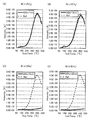
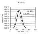
- FIG. 6A and 6B are a block diagram and a circuit diagram of a display device. FIG. 14 is a block diagram of a display device. FIG. 2 is a block diagram of a storage device. FIG. 18 is a block diagram and a circuit diagram of a memory device. FIG. TDS analysis results. TDS analysis results. TDS analysis results. Sheet resistance measurement results. SIMS analysis results. SIMS analysis results. SIMS analysis results.
- the functions of the source and the drain of the transistor may be switched when the polarity of the transistor or the direction of current changes in circuit operation. Therefore, the terms source and drain can be used interchangeably.
- the term “electrically connected” includes the case where they are connected via "something having an electrical function".
- the “thing having an electrical function” is not particularly limited as long as it can transmit and receive electrical signals between connection targets.
- “those having some electrical action” include electrodes, wirings, switching elements such as transistors, resistance elements, inductors, capacitors, elements having various other functions, and the like.
- membrane and the term “layer” can be interchanged with each other.
- conductive layer and “insulating layer” may be interchangeable with the terms “conductive film” and “insulating film” in some cases.
- an off-state current is a drain current when the transistor is in an off state (also referred to as a non-conduction state or a cutoff state) unless otherwise specified.
- the off-state means a state in which the voltage Vgs between the gate and the source is lower than the threshold voltage Vth (higher than Vth in the p-channel transistor) in the n-channel transistor.
- Embodiment 1 In this embodiment, a semiconductor device of one embodiment of the present invention will be described. Hereinafter, a transistor which is an embodiment of a semiconductor device is described.
- One embodiment of the present invention is a transistor including a semiconductor layer in which a channel is formed, an gate insulating layer over the semiconductor layer, and a gate electrode over the gate insulating layer over an oxide-containing insulating layer.
- the semiconductor layer is configured to include a metal oxide exhibiting semiconductor characteristics (hereinafter, also referred to as an oxide semiconductor).
- the semiconductor layer includes a channel formation region in which a channel can be formed and a pair of low resistance regions functioning as a source region and a drain region.
- the channel formation region is a region overlapping with the gate electrode in the semiconductor layer.
- An insulating layer containing metal nitride is provided in contact with the low resistance region.
- an effect of enhancing the conductivity of the low resistance region is exhibited.
- the metal nitride contains aluminum.
- an aluminum nitride film formed by a reactive sputtering method using aluminum as a sputtering target and a gas containing nitrogen as a film forming gas properly control the ratio of the flow rate of nitrogen gas to the total flow rate of the film forming gas
- the film can exhibit extremely high insulating properties and extremely high blocking properties against hydrogen and oxygen. Therefore, by providing an insulating film containing such a metal nitride in contact with the semiconductor layer, not only the resistance of the semiconductor layer is lowered, but also oxygen is released from the semiconductor layer, and hydrogen is released to the semiconductor layer. Diffusion can be suitably prevented.
- the thickness of the insulating layer containing the aluminum nitride is preferably 5 nm or more. Even with such a thin film, it is possible to achieve both the high blocking property to hydrogen and oxygen and the function of reducing the resistance of the semiconductor layer.
- the thickness of the insulating layer may be any thickness, it is preferably 500 nm or less, preferably 200 nm or less, more preferably 50 nm or less in consideration of productivity.
- an interlayer insulating layer is provided over the insulating layer containing metal nitride.
- the gate electrode and the gate insulating layer are preferably provided so as to be embedded in the opening provided in the interlayer insulating layer.
- a gate insulating layer be provided so as to cover the side surface and the bottom surface of the gate electrode inside the opening.
- the top surfaces of the interlayer insulating layer, the insulating layer containing metal nitride, the gate insulating layer, and the gate electrode are preferably planarized.
- an insulating layer (first barrier layer) which hardly diffuses oxygen and hydrogen on each of the interlayer insulating layer, the insulating layer containing metal nitride, the gate insulating layer, and the gate electrode on the planarized surface It is preferable to form (also referred to as Thus, it is possible to preferably prevent the diffusion of hydrogen from above the gate electrode and the gate insulating layer and the desorption of oxygen from above.
- an insulating layer (also referred to as a second barrier layer) which hardly diffuses oxygen and hydrogen is preferably provided below the insulating layer containing an oxide which is a formation surface of the semiconductor layer.
- the insulating layer containing oxide is provided with an opening reaching the second barrier layer so as to surround one or more transistors, and in the opening, the second barrier layer and the insulating layer containing metal nitride are provided. It is preferable to set it as the structure which contact
- the semiconductor layer, the gate insulating layer, and the gate electrode of the transistor can be surrounded by the insulating layer containing metal nitride, the first barrier layer, and the second barrier layer.
- diffusion of hydrogen into the semiconductor layer and release of oxygen from the semiconductor layer can be suitably prevented, and a highly reliable transistor can be realized.
- the transistor of one embodiment of the present invention can be applied to various circuits and devices.
- a display device to which various circuits such as an arithmetic circuit, a memory circuit, a driver circuit, and an interface circuit mounted in an electronic device or the like, a liquid crystal element or an organic EL element, or various sensor devices are applied. It can be suitably used for a drive circuit or the like.
- FIG. 1A is a top view of the transistor 100
- FIG. 1B corresponds to a cross-sectional view of a cross section taken along dashed-dotted line A1-A2 in FIG. 1A
- FIG. 1A corresponds to a cross-sectional view taken along a dashed-dotted line B1-B2 shown in FIG.
- FIG. 1A some of components of the transistor 100 (a gate insulating layer or the like) are omitted.
- the direction of the dashed-dotted line A1-A2 may be referred to as a channel length direction
- the direction of the dashed-dotted line B1-B2 may be referred to as a channel width direction.
- FIG. 1A some of the components may be omitted and illustrated in the following drawings.
- the transistor 100 is provided over the substrate 102 and includes an insulating layer 103, an insulating layer 104, a semiconductor layer 108, an insulating layer 110, a conductive layer 112, an insulating layer 115, an insulating layer 118, an insulating layer 116, and the like.
- the insulating layer 103 and the insulating layer 104 are stacked over the substrate 102.
- the island-shaped semiconductor layer 108 is provided in contact with the top surface of the insulating layer 104.
- An insulating layer 115 and an insulating layer 118 are stacked over the insulating layer 104 and the semiconductor layer 108.
- the insulating layer 118 is provided with an opening in a region overlapping with the semiconductor layer 108.
- the insulating layer 115 is provided to cover the inner wall of the opening of the insulating layer 118.
- the insulating layer 110 is provided in contact with the side surface of the insulating layer 115 and the top surface of the semiconductor layer 108, and the conductive layer 112 is provided over the insulating layer 110.
- the insulating layer 110 is provided in contact with the side surface and the bottom surface of the conductive layer 112.
- the upper portions of the insulating layer 118, the insulating layer 115, the insulating layer 110, and the conductive layer 112 are planarized, and the insulating layer 116 is provided thereover.
- a part of the conductive layer 112 functions as a gate electrode.
- a part of the insulating layer 110 functions as a gate insulating layer.
- the transistor 100 is a so-called top gate transistor in which a gate electrode is provided over the semiconductor layer 108.
- the semiconductor layer 108 preferably contains a metal oxide.
- the semiconductor layer 108 is made of indium, M (M is gallium, aluminum, silicon, boron, yttrium, tin, copper, vanadium, beryllium, titanium, iron, nickel, germanium, zirconium, molybdenum, lanthanum, cerium, neodymium, It is preferable to have zinc and one or more selected from hafnium, tantalum, tungsten, or magnesium.
- M is preferably aluminum, gallium, yttrium or tin.
- an oxide containing indium, gallium, and zinc is preferably used as the semiconductor layer 108.
- the semiconductor layer 108 has a stacked structure in which a semiconductor layer 108 a and a semiconductor layer 108 b are sequentially stacked from the insulating layer 104 side.
- materials different in composition, materials different in crystallinity, or materials different in impurity concentration can be selected.
- a low-resistance region 108 n is shown in the vicinity of the surface of the semiconductor layer 108 in contact with the insulating layer 115.
- a region of the semiconductor layer 108 which overlaps with the conductive layer 112 functions as a channel formation region of the transistor 100.
- the low-resistance region 108 n functions as a source region or a drain region of the transistor 100.
- an insulating film containing metal nitride can be used as the insulating layer 115.
- the insulating layer 115 preferably contains nitrogen and at least one of metal elements such as aluminum, titanium, tantalum, tungsten, chromium, and ruthenium.
- a film containing aluminum and nitrogen is preferable because it has extremely high insulation.
- a film satisfying the composition formula AlN x (x is a real number greater than 0 and 2 or less, preferably x is a real number greater than 0.5 and 1.5 or less) Is preferred.
- the film can be excellent in insulating properties and thermal conductivity; therefore, the heat dissipation property of heat generated when the transistor 100 is driven can be improved.
- an aluminum titanium nitride film, a titanium nitride film, or the like can be used as the insulating layer 115.
- the region 108 n is a part of the semiconductor layer 108 and has a lower resistance than the channel formation region.
- a region where metallic indium is deposited or a region with high indium concentration is formed in the vicinity of the interface of the region 108n on the insulating layer 115 side. May be The presence of such a region may be observed by an analysis method such as X-ray photoelectron spectroscopy (XPS), for example.
- XPS X-ray photoelectron spectroscopy
- the region 108 n can also be referred to as a region where the carrier density is higher than that of the channel formation region, a region where the oxygen defect density is high, or a region which is n-type.
- an oxide film is preferably used for the insulating layer 104 and the insulating layer 110 which are in contact with the channel formation region of the semiconductor layer 108.
- an oxide film such as a silicon oxide film, a silicon oxynitride film, or an aluminum oxide film can be used. Accordingly, oxygen released from the insulating layer 104 and the insulating layer 110 can be supplied to the channel formation region of the semiconductor layer 108 by heat treatment or the like in the manufacturing process of the transistor 100, and oxygen vacancies in the semiconductor layer 108 can be reduced. .
- an insulating film which hardly diffuses oxygen and hydrogen is preferably used.
- a metal oxide film such as an aluminum oxide film, a hafnium oxide film, or a hafnium aluminate film is preferably used.
- Aluminum oxide films, hafnium oxide films, hafnium aluminate films and the like have extremely high barrier properties even when the film thickness is thin. Therefore, the thickness can be 0.5 nm to 50 nm, preferably 1 nm to 40 nm, and more preferably 2 nm to 30 nm. In particular, since the aluminum oxide film has a high barrier property to hydrogen and the like, a sufficient effect can be obtained even if it is extremely thin (for example, 0.5 nm or more and 1.5 nm or less).
- the insulating layer 103 and the insulating layer 116 are preferably formed by a deposition method such as a sputtering method or an atomic layer deposition (ALD) method.
- the ALD method can form a film having high barrier properties because it can form a very dense film with high step coverage.
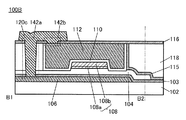
- FIGS. 1B and 1C a cross section of the peripheral portion of the semiconductor device is shown.
- part of the insulating layer 104 is removed by etching to form an opening, and the insulating layer 115 and the insulating layer 103 are in contact with each other in the opening.
- the transistor 100 in the block is an insulating layer.
- a structure sealed with the insulating layer 116 and the insulating layer 115 can be employed. Accordingly, diffusion of hydrogen from the outside into the semiconductor layer 108 of the transistor 100 and diffusion of oxygen in the semiconductor layer 108 can be effectively suppressed.
- the insulating layer 118 may contain hydrogen
- the insulating layer 104 including an oxide film in contact with the semiconductor layer 108 and the insulating layer 110 are not in contact with the insulating layer 118 due to the insulating layer 115. ing. Therefore, even when hydrogen is contained in the insulating layer 118, the hydrogen is diffused to the semiconductor layer 108 through the insulating layer 104 and the insulating layer 110 by heat or the like in the process for manufacturing the transistor 100. Can be effectively prevented.
- Oxygen vacancies formed in the semiconductor layer 108 are problematic because they affect transistor characteristics. For example, when oxygen vacancies are formed in the semiconductor layer 108, hydrogen is bonded to the oxygen vacancies and can be a carrier supply source. When a carrier supply source is generated in the semiconductor layer 108, a change in the electrical characteristics of the transistor 100, typically, a shift in threshold voltage occurs. Therefore, in the semiconductor layer 108, the less oxygen vacancies, the better.
- the insulating film in the vicinity of the semiconductor layer 108 specifically, the insulating layer 110 located above the semiconductor layer 108 and the insulating layer 104 located below include an oxide film. It is a structure. By transferring oxygen from the insulating layer 104 and the insulating layer 110 to the semiconductor layer 108 by heat or the like in the manufacturing process, oxygen vacancies in the semiconductor layer 108 can be reduced.
- the semiconductor layer 108 preferably includes a region in which the atomic ratio of In is larger than the atomic ratio of M. As the atomic ratio of In is larger, the field-effect mobility of the transistor can be improved.
- the bonding force between In and oxygen is weaker than the bonding force between Ga and oxygen, and therefore, when the atomic ratio of In is large, the metal oxide film There is a tendency for oxygen deficiency to form. In addition, even when other metal elements shown by the above M are used instead of Ga, the same tendency is obtained. When many oxygen vacancies are present in the metal oxide film, the electrical characteristics of the transistor and the reliability thereof are degraded.
- a very large amount of oxygen can be supplied to the semiconductor layer 108 including a metal oxide; therefore, a metal oxide material with a large atomic ratio of In can be used.
- a transistor having extremely high field effect mobility, stable electrical characteristics, and high reliability can be realized.
- a metal oxide in which the atomic ratio of In is at least 1.5 times, at least 2 times, at least 3 times, at least 3.5 times, or at least 4 times the atomic ratio of M It can be used suitably.
- a display device with a narrow frame width (also referred to as a narrow frame) can be provided.
- a source driver in particular, a demultiplexer connected to an output terminal of a shift register included in the source driver
- display with a small number of wirings connected to a display device An apparatus can be provided.
- the semiconductor layer 108 has a region in which the atomic ratio of In is larger than the atomic ratio of M, if the crystallinity of the semiconductor layer 108 is high, the field effect mobility may be low.
- the crystallinity of the semiconductor layer 108 can be analyzed, for example, by analysis using X-ray diffraction (XRD) or analysis using a transmission electron microscope (TEM). .
- impurities such as hydrogen or moisture mixed in the semiconductor layer 108 cause problems because they affect transistor characteristics. Therefore, in the semiconductor layer 108, it is preferable that the amount of impurities such as hydrogen or moisture be as low as possible.
- the use of a metal oxide film with a low impurity concentration and a low density of defect states is preferable because a transistor having excellent electrical characteristics can be manufactured.
- the carrier density in the film can be lowered by lowering the impurity concentration and lowering the density of defect states (reducing oxygen deficiency).
- electrical characteristics also referred to as normally on
- a transistor using such a metal oxide film can have extremely low off-state characteristics.
- the semiconductor layer 108 may have a stacked structure of two or more layers.
- the semiconductor layer 108 in which two or more metal oxide films different in composition are stacked can be used.
- the semiconductor layer 108 in which two or more metal oxide films having different crystallinity are stacked can be used.
- the same oxide target is preferably used, and the film formation conditions are preferably different so that the oxide target is continuously formed without being exposed to the air.
- the oxygen flow rate ratio at the time of film formation of the first metal oxide film (semiconductor layer 108a) to be formed first is the oxygen flow rate at the time of film formation of the second metal oxide film (semiconductor layer 108b) to be formed later Make it smaller than the ratio.
- oxygen is not flowed at the time of forming the first metal oxide film.
- oxygen can be effectively supplied at the time of film formation of the second metal oxide film.
- the first metal oxide film has lower crystallinity than the second metal oxide film, and can be a film having high electrical conductivity.
- the second metal oxide film provided on the upper side is a film having higher crystallinity than the first metal oxide film, damage is caused when the semiconductor layer 108 is processed or when the insulating layer 110 is formed. Can be suppressed.
- the oxygen flow ratio at the time of film formation of the first metal oxide film is 0% or more and less than 50%, preferably 0% or more and 30% or less, more preferably 0% or more and 20% or less, In fact, it is 10%.
- the oxygen flow rate ratio at the time of film formation of the second metal oxide film is 50% to 100%, preferably 60% to 100%, more preferably 80% to 100%, further preferably 90% or more 100% or less, typically 100%.
- conditions such as pressure, temperature, and electric power at the time of film formation may be different between the first metal oxide film and the second metal oxide film, conditions other than the oxygen flow ratio are the same. This is preferable because the time required for the film formation process can be shortened.
- the transistor 100 With such a configuration, the transistor 100 with excellent electrical characteristics and high reliability can be realized.
- FIG. 2A is a top view of the transistor 100A
- FIG. 2B is a cross-sectional view of the transistor 100A in the channel length direction
- FIG. 2C is a cross-sectional view of the transistor 100A in the channel width direction. It is.
- the transistor 100A is mainly different from Structural Example 1 in that the conductive layer 106 is provided between the substrate 102 and the insulating layer 103.
- the conductive layer 106 has a portion overlapping with the semiconductor layer 108 and the conductive layer 112 with the insulating layer 103 and the insulating layer 104 interposed therebetween.
- the conductive layer 106 has a function as a first gate electrode (also referred to as a bottom gate electrode), and the conductive layer 112 has a function as a second gate electrode (also referred to as a top gate electrode).
- part of the insulating layer 103 and the insulating layer 104 function as a first gate insulating layer, and part of the insulating layer 110 functions as a second gate insulating layer.
- a portion of the semiconductor layer 108 which overlaps with at least one of the conductive layer 112 and the conductive layer 106 functions as a channel formation region. Note that in the following, a portion overlapping with the conductive layer 112 of the semiconductor layer 108 may be referred to as a channel formation region for ease of description; however, in reality, the portion does not overlap with the conductive layer 112 but overlaps with the conductive layer 106 A channel can also be formed in a portion (including a part of the region 108n).
- the conductive layer 106 can be formed using the same material as the conductive layer 112, the conductive layer 120a, or the conductive layer 120b.
- the conductive layer 106 is preferably formed using a material containing copper because resistance can be reduced.
- the conductive layer 112 and the conductive layer 106 preferably protrude outward beyond the end portion of the semiconductor layer 108 in the channel width direction.
- the whole of the semiconductor layer 108 in the channel width direction is covered with the conductive layer 112 and the conductive layer 106 with the insulating layer 110, the insulating layer 103, and the insulating layer 104 interposed therebetween.
- the semiconductor layer 108 can be electrically surrounded by an electric field generated by the pair of gate electrodes.
- the same potential is preferably applied to the conductive layer 106 and the conductive layer 112. Accordingly, an electric field for inducing a channel can be effectively applied to the semiconductor layer 108, so that the on-state current of the transistor 100A can be increased. Therefore, the transistor 100A can be miniaturized.
- a constant potential may be applied to one of the conductive layer 112 and the conductive layer 106, and a signal for driving the transistor 100A may be supplied to the other.
- the threshold voltage in driving the transistor 100A with the other gate electrode can also be controlled by the potential supplied to the one gate electrode.
- FIG. 3 shows an example in which a conductive layer 120c which is formed in the same step as the conductive layer 120a and the like is provided over the insulating layer 116.
- the conductive layer 120 c is electrically connected to the conductive layer 106 through an opening 142 a provided in the insulating layer 116, the insulating layer 118, the insulating layer 104, and the insulating layer 103 in a partial region.
- the conductive layer 120 c is electrically connected to the conductive layer 112 through an opening 142 b provided in the insulating layer 116 in another portion. Accordingly, the same potential can be applied to the conductive layer 106 and the conductive layer 112.
- FIGS. 4A and 4B are a cross-sectional view of the transistor 100C in the channel length direction and a cross-sectional view of the transistor 100C in the channel width direction, respectively.
- the transistor 100C is mainly different from the above configuration example 1 in that the configuration of the semiconductor layer 108 is different.
- the semiconductor layer 108 includes a semiconductor layer 108c.
- the semiconductor layer 108 c is provided in the opening of the insulating layer 118 so as to be located between the insulating layer 110 and the insulating layer 115 and between the insulating layer 110 and the semiconductor layer 108 b.
- the semiconductor layer 108c can be formed using the same material as or a material different from one of the semiconductor layer 108a and the semiconductor layer 108b.
- a material which is different in at least one of crystallinity, composition, and impurity concentration from one or both of the semiconductor layer 108a and the semiconductor layer 108b can be used.
- a semiconductor layer in a channel formation region is formed at the time of film formation of the semiconductor film by increasing the flow ratio of oxygen gas to the total flow of the film formation gas.
- Oxygen can be effectively supplied to the semiconductor layer 108 b and the semiconductor layer 108 a.
- the flow rate ratio of the oxygen gas is 50% to 100%, preferably 70% to 100%, more preferably 90% to 100%, and further preferably 100%.
- FIG. 4C is a cross-sectional view of the transistor 100D in the channel length direction.
- the transistor 100D is mainly different from the above configuration example 1 in that the semiconductor layer 108 has a single-layer structure.
- the manufacturing process can be simplified.
- FIG. 4C shows an example in which the insulating layer 119 is further provided over the insulating layer 116, and the conductive layer 120a and the conductive layer 120b are provided over the insulating layer 119.
- Providing the insulating layer 119 is preferable because parasitic capacitance between the conductive layer 112 and the conductive layer 120 a or the conductive layer 120 b can be reduced.
- the conductive layer 106 described in Structural Example 2 can be provided in the transistor 100C and the transistor 100D.
- the material of the substrate 102 and the like are not particularly limited, but at least the heat resistance needs to be able to withstand the heat treatment to be performed later.
- a single crystal semiconductor substrate made of silicon or silicon carbide, a polycrystalline semiconductor substrate, a compound semiconductor substrate such as silicon germanium, an SOI substrate, a glass substrate, a ceramic substrate, a quartz substrate, a sapphire substrate or the like is used as the substrate 102. It is also good.
- a substrate provided with a semiconductor element over these substrates may be used as the substrate 102.
- a flexible substrate may be used as the substrate 102, and the transistor 100 and the like may be formed directly on the flexible substrate.
- a peeling layer may be provided between the substrate 102 and the transistor 100 or the like. The release layer can be used for separation from the substrate 102 and reprinting onto another substrate after a semiconductor device is partially or entirely completed thereon. At that time, the transistor 100 and the like can be transferred to a substrate with low heat resistance or a flexible substrate.
- the insulating layer 104 can be formed by a sputtering method, a CVD method, an evaporation method, a pulsed laser deposition (PLD) method, or the like as appropriate.
- the insulating layer 104 can be formed, for example, as a single layer or a stack of an oxide insulating film or a nitride insulating film. Note that in order to improve interface characteristics with the semiconductor layer 108, at least a region in contact with the semiconductor layer 108 in the insulating layer 104 is preferably formed using an oxide insulating film.
- a film which releases oxygen by heating is preferably used for the insulating layer 104.
- the insulating layer 104 for example, silicon oxide, silicon oxynitride, silicon nitride oxide, silicon nitride, aluminum oxide, hafnium oxide, gallium oxide, Ga-Zn oxide, or the like may be used, and a single layer or stacked layers can be provided.
- the surface in contact with the semiconductor layer 108 is subjected to pretreatment such as oxygen plasma treatment; Preferably, or near the surface is oxidized.
- the conductive layer 112 and the conductive layer 106 which function as a gate electrode and the conductive layer 120 a which functions as one of a source electrode and a drain electrode and the conductive layer 120 b which functions as the other include chromium, copper, aluminum, gold, silver, and zinc. Or a metal element selected from molybdenum, tantalum, titanium, tungsten, manganese, nickel, iron, cobalt, or an alloy containing the above-described metal element as a component, or an alloy or the like combining the above-described metal elements be able to.
- an In-Sn oxide, an In-W oxide, an In-W-Zn oxide, an In-Ti oxide, an In-Ti, or the like can be used for the conductive layer 112, the conductive layer 106, the conductive layer 120a, and the conductive layer 120b.
- An oxide conductor or metal oxide film such as -Sn oxide, In-Zn oxide, In-Sn-Si oxide, or In-Ga-Zn oxide can also be applied.
- oxide conductor Oxide Conductor
- OC Oxide Conductor
- a donor level is formed in the vicinity of the conduction band.
- the metal oxide becomes highly conductive and becomes conductive.
- a conductive metal oxide can be referred to as an oxide conductor.
- the conductive layer 112 or the like may have a stacked-layer structure of a conductive film containing the above-described oxide conductor (metal oxide) and a conductive film containing a metal or an alloy.
- the wiring resistance can be reduced by using a conductive film containing a metal or an alloy.
- a conductive film including an oxide conductor is preferably applied to the side in contact with the insulating layer which functions as a gate insulating film.
- the conductive layer 112, the conductive layer 106, the conductive layer 120a, and the conductive layer 120b preferably include one or more selected from titanium, tungsten, tantalum, and molybdenum among the above-described metal elements. It is suitable. In particular, it is preferable to use a tantalum nitride film.
- the tantalum nitride film is a conductive film in contact with the semiconductor layer 108 because the tantalum nitride film has conductivity, high barrier properties against copper, oxygen, or hydrogen and little release of hydrogen from itself.
- the conductive film can be suitably used as a conductive film in the vicinity of the semiconductor layer 108.
- the insulating layer 110 functioning as a gate insulating film of the transistor 100 or the like can be formed by a PECVD method, a sputtering method, or the like.
- An insulating layer containing one or more of a film, a lanthanum oxide film, a cerium oxide film, and a neodymium oxide film can be used.
- the insulating layer 110 may have a stacked structure of two layers or a stacked structure of three or more layers.
- the insulating layer 110 in contact with the semiconductor layer 108 is preferably an oxide insulating film, and more preferably has a region containing oxygen in excess of the stoichiometric composition.
- the insulating layer 110 is an insulating film capable of releasing oxygen.
- the insulating layer 110 is formed in an oxygen atmosphere, heat treatment in an oxygen atmosphere, plasma treatment, or the like is performed on the insulating layer 110 after film formation, or over the insulating layer 110 in an oxygen atmosphere.
- Oxygen can also be supplied to the insulating layer 110 by forming an oxide film or the like.
- the insulating layer 110 a material such as hafnium oxide having a higher relative dielectric constant than silicon oxide or silicon oxynitride can be used.
- the film thickness of the insulating layer 110 can be increased to suppress the leak current due to the tunnel current.
- hafnium oxide having crystallinity is preferable because it has a high dielectric constant as compared to amorphous hafnium oxide.
- the sputtering target used to form the In-M-Zn oxide preferably has an atomic ratio of In greater than or equal to an atomic ratio of M.
- the atomic ratio of the semiconductor layer 108 to be formed includes a variation of plus or minus 40% of the atomic ratio of the metal element contained in the above sputtering target.
- the atomic ratio of Ga is 1 or more and 3 or less, where the atomic ratio of In is 4.
- the atomic ratio of is 2 or more and 4 or less is included.
- the atomic ratio of Ga is larger than 0.1. It is 2 or less, and the case where the atomic ratio of Zn is 5 or more and 7 or less is included.
- the semiconductor layer 108 has an energy gap of 2 eV or more, preferably 2.5 eV or more.
- the off-state current of the transistor can be reduced.
- the semiconductor layer 108 preferably has a non-single-crystal structure.
- the non-single crystal structure includes, for example, a CAAC structure, a polycrystalline structure, a microcrystalline structure, or an amorphous structure described later.
- the amorphous structure has the highest density of defect states
- the CAAC structure has the lowest density of defect states.
- CAAC c-axis aligned crystal
- the CAAC structure is one of crystal structures such as a thin film having a plurality of nanocrystals (crystal regions having a maximum diameter of less than 10 nm), and each nanocrystal has c axis oriented in a specific direction and an a axis And b axes are crystal structures having a feature that nanocrystals are continuously connected without forming grain boundaries without having orientation.
- a thin film having a CAAC structure is characterized in that the c-axis of each nanocrystal is easily oriented in the thickness direction of the thin film, the normal direction of the formation surface, or the normal direction of the surface of the thin film.
- CAAC-OS Oxide Semiconductor
- CAAC-OS is an oxide semiconductor with high crystallinity.
- CAAC-OS can not confirm clear crystal grain boundaries, so that it can be said that the decrease in electron mobility due to crystal grain boundaries does not easily occur.
- the crystallinity of the oxide semiconductor may be lowered due to the mixing of impurities, generation of defects, or the like, so that the CAAC-OS can also be said to be an oxide semiconductor with few impurities or defects (such as oxygen vacancies). Therefore, the oxide semiconductor having a CAAC-OS has stable physical properties. Therefore, an oxide semiconductor having a CAAC-OS is resistant to heat and has high reliability.
- crystallography it is general to take a unit cell with c-axis as a specific axis with respect to three axes (crystal axes) of a-axis, b-axis, and c-axis constituting the unit cell.
- crystal axes three axes
- b-axis a axis
- c-axis constituting the unit cell.
- two axes parallel to the plane direction of the layer are the a axis and b axis
- an axis intersecting the layer is the c axis.
- a typical example of a crystal having such a layered structure is graphite classified into a hexagonal system, and the a-axis and b-axis of the unit cell are parallel to the cleavage plane and the c-axis is orthogonal to the cleavage plane Do.
- a crystal of InGaZnO 4 having a layered crystal structure of YbFe 2 O 4 type can be classified into a hexagonal system, and the a-axis and b-axis of the unit cell are parallel to the plane direction of the layer and c-axis Is orthogonal to the layers (ie, the a and b axes).
- a metal oxide formed by sputtering at a substrate temperature of 100 ° C. to 130 ° C. using the above target has a crystal structure of any one of nc (nano crystal) structure and CAAC structure, or a structure in which these are mixed.
- nc nano crystal
- CAAC room temperature
- a metal oxide formed by a sputtering method with a substrate temperature of room temperature (RT) tends to have a nc crystal structure.
- the room temperature (R.T.) referred to here includes the temperature when the substrate is not intentionally heated.
- thin films insulating films, semiconductor films, conductive films, and the like that constitute a semiconductor device are formed by sputtering, chemical vapor deposition (CVD), vacuum evaporation, pulse laser deposition (PLD: Pulse Laser Deposition). ), Atomic layer deposition (ALD), or the like.
- CVD chemical vapor deposition
- PLA Pulse Laser Deposition
- ALD Atomic layer deposition
- CVD method include plasma enhanced chemical vapor deposition (PECVD), thermal CVD and the like.
- PECVD plasma enhanced chemical vapor deposition
- MOCVD metal organic chemical vapor deposition
- thin films (insulating films, semiconductor films, conductive films, etc.) constituting a semiconductor device can be spin-coated, dip, spray-coated, inkjet, dispensing, screen printing, offset printing, doctor knife, slit coat, roll coat, curtain coat , Knife coating or the like.
- the thin film when processing a thin film forming the semiconductor device, can be processed using a photolithography method or the like.
- the thin film may be processed by a nanoimprint method, a sand blast method, a lift-off method or the like.
- the island-shaped thin film may be formed directly by a film formation method using a shielding mask such as a metal mask.
- the photolithography method there are typically the following two methods.
- One is a method of forming a resist mask on a thin film to be processed, processing the thin film by etching or the like, and removing the resist mask.
- the other is a method of processing the thin film into a desired shape by forming a thin film having photosensitivity, followed by exposure and development.
- light used for exposure may be, for example, i-ray (wavelength 365 nm), g-ray (wavelength 436 nm), h-ray (wavelength 405 nm), or a mixture of these.
- ultraviolet light, KrF laser light, ArF laser light or the like can also be used.
- the exposure may be performed by the immersion exposure technique.
- extreme ultraviolet (EUV: Extreme Ultra-violet) or X-rays may be used.
- an electron beam can be used instead of light used for exposure. The use of extreme ultraviolet light, X-rays or electron beams is preferable because extremely fine processing is possible. In the case where exposure is performed by scanning a beam such as an electron beam, a photomask is not necessary.
- etching of the thin film a dry etching method, a wet etching method, a sand blast method, or the like can be used.
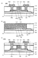
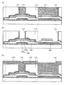
- FIGS. 5 to 8 the cross sections in the channel length direction and the channel width direction in each step of the manufacturing process of the transistor 100A are shown side by side.
- the left side of each drawing shows a cross section of the peripheral portion of the semiconductor device.
- a conductive film is formed over the substrate 102 and processed by etching to form a conductive layer 106 which functions as a gate electrode (FIG. 5A).
- the insulating layer 103 and the insulating layer 104 are stacked to cover the substrate 102 and the conductive layer 106 (FIG. 5B).
- the insulating layer 103 and the insulating layer 104 can each be formed by a PECVD method, an ALD method, a sputtering method, or the like.
- the insulating layer 103 can be formed by an ALD method or a sputtering method
- the insulating layer 104 can be formed by a PECVD method or a sputtering method.
- part of the insulating layer 104 located at an end portion of the semiconductor device is removed by etching (FIG. 5C).
- the metal oxide film 108af and the metal oxide film 108bf are preferably formed by a sputtering method using a metal oxide target.
- an inert gas eg, helium gas, argon gas, xenon gas, or the like
- oxygen flow ratio the ratio of oxygen gas to the whole of the deposition gas at the time of depositing the metal oxide film.
- oxygen flow ratio is 0% or more and 100% or less, preferably 5% or more and 20% or less It is preferable to do.
- the oxygen flow ratio is higher, the crystallinity of the metal oxide film can be improved, and a highly reliable transistor can be realized.
- the oxygen flow ratio is lower, the crystallinity of the metal oxide film is lowered, and a transistor in which the on current is increased can be obtained.
- the substrate temperature may be higher than or equal to room temperature and lower than 200 ° C., preferably, the substrate temperature may be higher than or equal to room temperature and 140 ° C. or lower.
- productivity is preferably high.
- the crystallinity can be reduced by forming the metal oxide film while the substrate temperature is at room temperature or in a state in which the substrate temperature is not intentionally heated.
- a process for removing water, hydrogen, an organic component, or the like adsorbed on the surface of the insulating layer 104, or a process for supplying oxygen to the insulating layer 104 is performed.
- heat treatment can be performed at a temperature of 70 ° C to 200 ° C in a reduced pressure atmosphere.
- plasma treatment may be performed in an atmosphere containing oxygen.
- organic substances on the surface of the insulating layer 104 can be preferably removed. After such treatment, it is preferable to form a metal oxide film continuously without exposing the surface of the insulating layer 104 to the air.
- the metal oxide film is processed to form an island-shaped semiconductor layer 108a and a semiconductor layer 108b (FIG. 5E).
- a wet etching method and a dry etching method may be used for processing of the metal oxide film.
- a wet etching method and a dry etching method may be used.
- part of the insulating layer 104 which does not overlap with the semiconductor layer 108 may be etched and thinned.
- heat treatment may be performed to remove hydrogen or water in the metal oxide film or the semiconductor layer 108.
- the temperature of the heat treatment is typically 150 ° C to less than the strain point of the substrate, or 250 ° C to 450 ° C, or 300 ° C to 450 ° C.
- the heat treatment can be performed in an atmosphere containing a rare gas or nitrogen. Alternatively, after heating in the atmosphere, heating may be performed in an atmosphere containing oxygen. Note that hydrogen, water, and the like are preferably not contained in the atmosphere of the heat treatment.
- an electric furnace, an RTA apparatus, or the like can be used for the heat treatment. The heat treatment time can be shortened by using the RTA apparatus.
- the dummy layer 113 is formed over the semiconductor layer 108 and the insulating layer 104 (FIG. 6A).
- the dummy layer 113 is a layer for forming an opening in which the later conductive layer 112 and the insulating layer 110 are provided.
- the dummy layer 113 can be formed by removing an unnecessary portion by etching after forming a thin film.
- a material of the dummy layer 113 it is preferable to appropriately select a material which can have a large selection ratio with the semiconductor layer 108 and the insulating layer 104 at the etching rate.
- a metal oxide film having crystallinity is used for the semiconductor layer 108b
- a metal oxide film having low crystallinity eg, having a microcrystalline structure
- part of the insulating layer 104 may be thinned.
- the thickness of the dummy layer 113 be formed thick in consideration of the reduction in thickness by the second planarization process performed later.
- the insulating layer 115 is formed to cover the insulating layer 104, the semiconductor layer 108, and the dummy layer 113 (FIG. 6B). At this time, a region where the insulating layer 115 and the insulating layer 103 are in contact with each other is formed at an end portion of the semiconductor device.
- the insulating layer 115 is preferably formed by a reactive sputtering method using a sputtering target containing the above metal element and a mixed gas of a nitrogen gas and a rare gas which is a dilution gas as a deposition gas.
- a reactive sputtering method using a sputtering target containing the above metal element and a mixed gas of a nitrogen gas and a rare gas which is a dilution gas as a deposition gas.
- the flow rate of nitrogen gas is 30% to 100%, preferably 40% to 100% of the total flow rate of the deposition gas. It is preferable to set it as 50% or more and 100% or less more preferably below.
- a low-resistance region 108 n is formed in a region in the vicinity of the interface of the semiconductor layer 108 in contact with the insulating layer 115.
- heat treatment is preferably performed.
- the heat treatment can further reduce the resistance of the region 108n of the semiconductor layer 108.
- the heat treatment is preferably performed in an inert gas atmosphere such as nitrogen or a rare gas.
- the temperature may be 120 ° C. to 500 ° C., preferably 150 ° C. to 450 ° C., more preferably 200 ° C. to 400 ° C., further preferably 250 ° C. to 400 ° C.
- semiconductor devices can be produced with high yield in a production facility using a large glass substrate.
- the heat treatment may be performed at any stage after the formation of the insulating layer 115.
- the heat treatment may be combined with another heat treatment.
- oxygen in the semiconductor layer 108 is extracted toward the insulating layer 115 by heat treatment, whereby oxygen vacancies are generated.
- the carrier concentration is increased by bonding of the oxygen vacancy and hydrogen contained in the semiconductor layer 108, so that a portion in contact with the insulating layer 115 can be lowered in resistance.
- the metal element contained in the semiconductor layer 108 is diffused toward the vicinity of the interface with the insulating layer 115 by heat treatment to form a region with a high concentration of the metal element, whereby the resistance can be reduced. is there.
- a region with a high indium concentration may be observed in the vicinity of the interface of the semiconductor layer 108 with the insulating layer 115.
- the region 108 n reduced in resistance by such a combined action becomes a very stable low resistance region.
- the region 108 n formed in this manner has a feature that it is difficult to increase the resistance again, for example, even when the process of supplying oxygen is performed in the later step.
- the insulating layer 118 is formed to cover the insulating layer 115 (FIG. 6C).
- the insulating layer 118 is preferably formed sufficiently thick in consideration of thinning of the insulating layer 118 by planarization treatment to be performed later.
- the insulating layer 118 can be formed by, for example, a PECVD method.
- planarization treatment typically, a polishing treatment such as chemical mechanical polishing (CMP) can be used.
- CMP chemical mechanical polishing
- dry etching or plasma treatment may be used. Note that the polishing treatment, the dry etching treatment, and the plasma treatment may be performed a plurality of times, or may be performed in combination. In the case of combining them, the order of steps is not particularly limited, and may be set appropriately in accordance with the uneven state of the surface to be treated.
- the dummy layer 113 is removed by etching (FIG. 7B).
- the opening of the insulating layer 118 is formed over the channel formation region of the semiconductor layer 108.
- a structure in which the insulating layer 115 is provided in contact with the inner wall of the opening portion of the insulating layer 118 can be formed.
- part of the insulating layer 104 may be thinned when the dummy layer 113 is etched.
- an oxide film such as a silicon oxide film or a silicon oxynitride film is preferably formed using a plasma enhanced chemical vapor deposition apparatus (referred to as a PECVD apparatus or simply referred to as a plasma CVD apparatus).
- a plasma enhanced chemical vapor deposition apparatus referred to as a PECVD apparatus or simply referred to as a plasma CVD apparatus.
- it may be formed by PECVD using microwaves.
- they can be formed by a CVD method using an organosilane gas.
- the conductive film 112 f include a material which suppresses permeation of oxygen.
- a material which suppresses permeation of oxygen For example, tantalum nitride, tungsten nitride, titanium nitride or the like can be used.
- the conductive film 112 f can be formed, for example, by a sputtering method, a CVD method, an MBE method, a PLD method, an ALD method, or the like.
- a lower conductive film is formed using a sputtering method, an ALD method, or the like, and then the upper conductive film is plated, sputtered, CVD, MBE, PLD A film can be formed using a method, an ALD method, or the like.
- voids and the like are less likely to be formed in the conductive film 112f to be embedded.
- a second planarization treatment is performed on the conductive film 112 f, the insulating film 110 f, the insulating layer 115, and the insulating layer 118 so that the upper portion of the insulating layer 118 is exposed (FIG. 8A).
- the second planarization process can be performed in the same manner as the first planarization process.
- the conductive layer 112 and the insulating layer 110 can be formed.
- the insulating layer 116 is formed over the insulating layer 118, the insulating layer 115, the insulating layer 110, and the conductive layer 112 (FIG. 8B).
- the insulating layer 116 can be formed by the same method as the insulating layer 103.
- second heat treatment is preferably performed.
- the second heat treatment can be performed under the same conditions as the first heat treatment.
- oxygen released from the insulating layer 104 can be supplied to the semiconductor layer 108, and oxygen vacancies in the semiconductor layer 108 can be reduced.
- oxygen released from the insulating layer 110 can be supplied to the channel formation region of the semiconductor layer 108.
- Openings 141a and 141b [Formation of Openings 141a and 141b] Subsequently, a mask is formed by lithography at a desired position of the insulating layer 116, and then the insulating layer 116, the insulating layer 118, and part of the insulating layer 115 are etched to form the opening 141a and the opening reaching the region 108n. The portion 141 b is formed.
- an opening 142 a reaching the conductive layer 106 and an opening 142 b reaching the conductive layer 112 may be formed in this step.
- the conductive layer 120c may be formed at the same time in this step.
- the transistor 100A can be manufactured.
- This embodiment can be implemented in appropriate combination with at least a part of the other embodiments described in this specification.
- FIG. 9A shows a top view of the display device 700.
- the display device 700 includes a first substrate 701 and a second substrate 705 which are attached by a sealant 712.
- the pixel portion 702, the source driver circuit portion 704, and the gate driver circuit portion 706 are provided over the first substrate 701.
- Be The pixel portion 702 is provided with a plurality of display elements.
- an FPC terminal portion 708 to which an FPC 716 (FPC: Flexible Printed Circuit) is connected is provided in a portion of the first substrate 701 which does not overlap with the second substrate 705.
- FPC 716 Flexible Printed Circuit
- Various signals and the like are supplied to the pixel portion 702, the source driver circuit portion 704, and the gate driver circuit portion 706 through the FPC terminal portion 708 and the signal line 710 by the FPC 716.
- a plurality of gate driver circuit units 706 may be provided.
- the gate driver circuit unit 706 and the source driver circuit unit 704 may be separately formed on a semiconductor substrate or the like and may be in the form of an IC chip packaged.
- the IC chip can be mounted over the first substrate 701 or the FPC 716.
- the transistors in the semiconductor device of one embodiment of the present invention can be applied to the transistors included in the pixel portion 702, the source driver circuit portion 704, and the gate driver circuit portion 706.
- a liquid crystal element, a light emitting element, or the like can be given.
- a transmissive liquid crystal element, a reflective liquid crystal element, a semi-transmissive liquid crystal element, or the like can be used.
- a light emitting element self-luminous light emitting elements, such as LED (Light Emitting Diode), OLED (Organic LED), QLED (Quantum-dot LED), a semiconductor laser, are mentioned.
- a shutter type or a light interference type MEMS (Micro Electro Mechanical Systems) element a display element to which a microcapsule type, an electrophoresis type, an electrowetting type, an electronic powder fluid (registered trademark) type, or the like is applied is used. It can also be done.
- MEMS Micro Electro Mechanical Systems
- the display device 700A illustrated in FIG. 9B is a display device which can be suitably used for an electronic device having a large screen.
- it can be suitably used for a television device, a monitor device, digital signage and the like.
- the display device 700A includes a plurality of source driver ICs 721 and a pair of gate driver circuits 722.
- the transistor which is the semiconductor device of one embodiment of the present invention can be applied to the transistor included in the pixel portion 702, the source driver IC 721, and the gate driver circuit 722.
- the plurality of source driver ICs 721 are attached to the FPC 723 respectively.
- one terminal is connected to the first substrate 701, and the other terminal is connected to the printed substrate 724.
- the printed substrate 724 can be provided on the back side of the pixel portion 702 and mounted on the electronic device, and space saving of the electronic device can be achieved.
- the gate driver circuit 722 is formed on the first substrate 701. Thereby, an electronic device with a narrow frame can be realized.
- a large-sized and high-resolution display device can be realized.
- the present invention can be applied to a display having a screen size of 30 inches or more, 40 inches or more, 50 inches or more, or 60 inches or more.
- a display device with extremely high resolution such as full high definition, 4K2K, or 8K4K can be realized.
- This embodiment can be implemented in appropriate combination with at least a part of the other embodiments described in this specification.
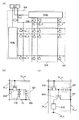
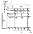
- the display device illustrated in FIG. 10A includes a pixel portion 502, a driver circuit portion 504, a protective circuit 506, and a terminal portion 507. Note that the protective circuit 506 may not be provided.
- part or all of the driver circuit portion 504 be formed over the same substrate as the pixel portion 502. Thereby, the number of parts and the number of terminals can be reduced.
- part or all of the driver circuit portion 504 is formed by COG or TAB (Tape Automated Bonding). It can be implemented.
- the transistor of one embodiment of the present invention can be applied to the transistor included in the driver circuit portion 504.
- the transistor of one embodiment of the present invention may be applied to the pixel portion 502 and the protective circuit 506.
- the pixel portion 502 includes a pixel circuit 501 for driving a plurality of display elements arranged in X rows (X is a natural number of 2 or more) and Y columns (Y is a natural number of 2 or more).
- a driver circuit such as a gate driver 504a which outputs a scan signal to GL_1 to GL_X and a source driver 504b which supplies a data signal to data lines DL_1 to DL_Y are included.
- the gate driver 504a may be configured to have at least a shift register.
- the source driver 504 b is configured using, for example, a plurality of analog switches. Alternatively, the source driver 504 b may be configured using a shift register or the like.
- a terminal portion 507 is a portion provided with a terminal for inputting a power supply, a control signal, and an image signal from an external circuit to the display device.
- the protective circuit 506 is a circuit which brings a wiring and another wiring into conduction when the wiring to which the protection circuit 506 is connected is supplied with a potential outside the predetermined range.
- the protective circuit 506 illustrated in FIG. 10A is, for example, a scanning line GL which is a wiring between the gate driver 504 a and the pixel circuit 501 or a data line DL which is a wiring between the source driver 504 b and the pixel circuit 501. It is connected to various wiring.
- the gate driver 504 a and the source driver 504 b may be provided over the same substrate as the pixel portion 502, or a substrate on which a separately prepared gate driver circuit or source driver circuit is formed (for example, a single crystal semiconductor)
- a driver circuit substrate formed of a film or a polycrystalline semiconductor film may be mounted.
- FIG. 11 shows a configuration different from that of FIG.
- a pair of source lines for example, the source line DLa1 and the source line DLb1 are disposed so as to sandwich a plurality of pixels arranged in the source line direction.
- two adjacent gate lines for example, the gate line GL_1 and the gate line GL_2 are electrically connected.
- the pixels connected to the gate line GL_1 are connected to one of the source lines (the source line DLa1, the source line DLa2, etc.), and the pixels connected to the gate line GL_2 are the other source line (the source line DLb1, the source Are connected to line DLb2 etc.).
- the plurality of pixel circuits 501 illustrated in FIGS. 10A and 11 can be configured as illustrated in FIGS. 10B and 10C, for example.
- the pixel circuit 501 illustrated in FIG. 10B includes a liquid crystal element 570, a transistor 550, and a capacitor 560. Further, to the pixel circuit 501, a data line DL_n, a scanning line GL_m, a potential supply line VL, and the like are connected. The transistor described in the above embodiment may be applied to the transistor 550.
- the potential of one of the pair of electrodes of the liquid crystal element 570 is appropriately set in accordance with the specification of the pixel circuit 501.
- the alignment state of the liquid crystal element 570 is set by the data to be written. Note that a common potential (common potential) may be applied to one of the pair of electrodes of the liquid crystal element 570 included in each of the plurality of pixel circuits 501. Further, different potentials may be applied to one of the pair of electrodes of the liquid crystal element 570 of the pixel circuit 501 in each row.
- the pixel circuit 501 illustrated in FIG. 10C includes transistors 552 and 554, a capacitor 562, and a light-emitting element 572. Further, to the pixel circuit 501, a data line DL_n, a scanning line GL_m, a potential supply line VL_a, and the like are connected. The transistor described in the above embodiment may be applied to one or both of the transistor 552 and the transistor 554.
- an organic electroluminescent element also referred to as an organic EL element
- the light emitting element 572 is not limited to this, and an inorganic EL element containing an inorganic material may be used.
- the high power supply potential VDD is applied to one of the potential supply line VL_a and the potential supply line VL_b, and the low power supply potential VSS is applied to the other.
- This embodiment can be implemented in appropriate combination with at least a part of the other embodiments described in this specification.
- Embodiment 4 In this embodiment, a DOSRAM is described as an example of a memory device to which a transistor and a capacitor of one embodiment of the present invention are applied, with reference to FIGS. 12 and 13.
- DOSRAM registered trademark
- Dynamic Oxide Semiconductor RAM is an abbreviation of "Dynamic Oxide Semiconductor RAM", and refers to a RAM having memory cells of 1T (transistor) 1C (capacitance) type.
- FIG. 12 shows a configuration example of the DOSRAM.
- the DOSRAM 1400 has a controller 1405, a row circuit 1410, a column circuit 1415, a memory cell and a sense amplifier array (hereinafter referred to as "MC-SA array 1420").
- MC-SA array 1420 a sense amplifier array
- the row circuit 1410 includes a decoder 1411, a word line driver circuit 1412, a column selector 1413, and a sense amplifier driver circuit 1414.
- the column circuit 1415 has a global sense amplifier array 1416 and an input / output circuit 1417.
- the global sense amplifier array 1416 has a plurality of global sense amplifiers 1447.
- the MC-SA array 1420 has a memory cell array 1422, a sense amplifier array 1423, and global bit lines GBLL and GBLR.
- the MC-SA array 1420 has a stacked structure in which the memory cell array 1422 is stacked on the sense amplifier array 1423.
- Global bit lines GBLL and GBLR are stacked on memory cell array 1422.
- a hierarchical bit line structure hierarchized by local bit lines and global bit lines is adopted as the structure of bit lines.
- Memory cell array 1422 includes N (N is an integer of 2 or more) local memory cell arrays 1425 ⁇ 0> to 1425 ⁇ N-1>.
- N is an integer of 2 or more
- the local memory cell array 1425 has a plurality of memory cells 1445, a plurality of word lines WL, and a plurality of bit lines BLL and BLR.
- the structure of the local memory cell array 1425 is an open bit line type, but may be a folded bit line type.
- FIG. 13B shows an example of a circuit configuration of a pair of memory cells 1445a and 1445b connected to a common bit line BLL (BLR).
- the memory cell 1445a includes a transistor MW1a, a capacitive element CS1a, and terminals B1a and B2a, and is connected to the word line WLa and the bit line BLL (BLR).
- the memory cell 1445 b has a transistor MW 1 b, a capacitive element CS 1 b, terminals B 1 b and B 2 b, and is connected to the word line WLb and the bit line BLL (BLR). Note that, in the following, when one of the memory cell 1445a and the memory cell 1445b is not particularly limited, the memory cell 1445 and the configuration attached to the memory cell 1445 may not be denoted by the symbol a or b.
- the transistor MW1a has a function of controlling charging and discharging of the capacitive element CS1a
- the transistor MW1b has a function of controlling charging and discharging of the capacitive element CS1b.
- the gate of transistor MW1a is electrically connected to word line WLa, the first terminal is electrically connected to bit line BLL (BLR), and the second terminal is electrically connected to the first terminal of capacitive element CS1a.
- the gate of transistor MW1b is electrically connected to word line WLb, the first terminal is electrically connected to bit line BLL (BLR), and the second terminal is electrically connected to the first terminal of capacitive element CS1b. It is done.
- the bit line BLL (BLR) is commonly used for the first terminal of the transistor MW1a and the first terminal of the transistor MW1b.
- the transistor MW1 has a function of controlling charging and discharging of the capacitive element CS1.
- the second terminal of the capacitive element CS1 is electrically connected to the terminal B2.
- a constant voltage (for example, low power supply voltage) is input to the terminal B2.
- the semiconductor device described in the above embodiment can be applied to the transistor MW1a of the memory cells 1445a and 1445b.
- the transistor MW1 has a back gate, and the back gate is electrically connected to the terminal B1. Therefore, the threshold voltage of the transistor MW1 can be changed by the voltage of the terminal B1.
- the voltage of the terminal B1 may be a fixed voltage (for example, a negative constant voltage), or the voltage of the terminal B1 may be changed according to the operation of the DOS RAM 1400.
- the back gate of the transistor MW1 may be electrically connected to the gate, the source, or the drain of the transistor MW1. Alternatively, the transistor MW1 may not be provided with a back gate.
- Sense amplifier array 1423 includes N local sense amplifier arrays 1426 ⁇ 0> to 1426 ⁇ N-1>.
- the local sense amplifier array 1426 includes one switch array 1444 and a plurality of sense amplifiers 1446.
- a bit line pair is electrically connected to sense amplifier 1446.
- the sense amplifier 1446 has a function of precharging the bit line pair, a function of amplifying a voltage difference between the bit line pair, and a function of holding the voltage difference.
- the switch array 1444 has a function of selecting a bit line pair and conducting between the selected bit line pair and the global bit line pair.
- the controller 1405 has a function of controlling the overall operation of the DOS RAM 1400.
- the controller 1405 performs a logical operation on an externally input command signal to determine an operation mode, and generates a control signal for the row circuit 1410 and the column circuit 1415 so that the determined operation mode is executed. And a function of holding an address signal input from the outside, and a function of generating an internal address signal.
- the row circuit 1410 has a function of driving the MC-SA array 1420.
- the decoder 1411 has a function of decoding an address signal.
- the word line driver circuit 1412 generates a selection signal for selecting the word line WL in the access target row.
- the column selector 1413 and the sense amplifier driver circuit 1414 are circuits for driving the sense amplifier array 1423.
- the column selector 1413 has a function of generating a selection signal for selecting a bit line of the access target column.
- the selection signal of column selector 1413 controls switch array 1444 of each local sense amplifier array 1426.
- the control signals of the sense amplifier driver circuit 1414 drive the plurality of local sense amplifier arrays 1426 independently.
- Column circuit 1415 has a function of controlling an input of data signal WDA [31: 0] and a function of controlling an output of data signal RDA [31: 0].
- the data signal WDA [31: 0] is a write data signal
- the data signal RDA [31: 0] is a read data signal.
- Global sense amplifier 1447 is electrically connected to global bit line pair (GBLL, GBLR).
- the global sense amplifier 1447 has a function of amplifying a voltage difference between the global bit line pair (GBLL, GBLR) and a function of holding this voltage difference. Writing and reading of data to the global bit line pair (GBLL, GBLR) are performed by the input / output circuit 1417.
- the number of times of rewriting is not limited in principle in the DOSRAM 1400, and data can be written and read with low energy.
- the circuit configuration of the memory cell 1445 is simple, the capacity can be easily increased.
- the transistor MW1 is a transistor to which an oxide semiconductor is applied, and has extremely low off-state current, whereby charge leakage from the capacitor CS1 can be suppressed. Therefore, the retention time of the DOS RAM 1400 is very long compared to the DRAM. Therefore, since the frequency of refresh can be reduced, the power required for the refresh operation can be reduced. Therefore, the DOSRAM 1400 is suitable for a memory device that rewrites a large amount of data with high frequency, for example, a frame memory used for image processing.
- bit lines can be shortened to a length approximately equal to the length of local sense amplifier array 1426. By shortening the bit line, the bit line capacitance can be reduced and the storage capacitance of the memory cell 1445 can be reduced. Further, by providing the switch array 1444 in the local sense amplifier array 1426, the number of long bit lines can be reduced. From the above reasons, the load driven at the time of access to the DOS RAM 1400 is reduced, and power consumption can be reduced.
- This embodiment can be implemented in appropriate combination with at least a part of the other embodiments described in this specification.
- FIG. 14 illustrates a specific example of an electronic device using the semiconductor device according to one embodiment of the present invention.
- the monitor 830 is shown in FIG.
- the monitor 830 includes a display portion 831, a housing 832, a speaker 833, and the like. Furthermore, an LED lamp, an operation key (including a power switch or an operation switch), a connection terminal, various sensors, a microphone, and the like can be included.
- the monitor 830 can be operated by the remote controller 834.
- the monitor 830 can also function as a television device by receiving broadcast waves.
- Examples of broadcast radio waves that can be received by the monitor 830 include terrestrial waves, radio waves transmitted from satellites, and the like, and include analog broadcasts and digital broadcasts. Further, for example, by using a plurality of data received in a plurality of frequency bands, the transfer rate can be increased, and an image having a resolution exceeding full high definition can be displayed on the display portion 831. For example, an image having a resolution of 4K2K, 8K4K, 16K8K, or higher can be displayed.
- the monitor 830 can be connected to a computer and used as a computer monitor. The monitor 830 can also be used as digital signage.
- the semiconductor device of one embodiment of the present invention can be used for a driver circuit of a display portion or an image processing portion.
- the semiconductor device of one embodiment of the present invention for a driver circuit of a display portion or an image processing portion, high-speed operation and signal processing can be realized with low power consumption.
- image processing such as noise removal processing, tone conversion processing, color tone correction processing, and luminance correction processing can be performed. it can. Further, it is possible to execute inter-pixel interpolation processing accompanying resolution up-conversion and inter-frame interpolation processing accompanying frame frequency up-conversion. Further, in the gradation conversion process, not only conversion of the number of gradations of an image, but also interpolation of gradation values in the case of increasing the number of gradations can be performed. Also, high dynamic range (HDR) processing, which extends the dynamic range, is also included in the tone conversion processing.
- HDR high dynamic range
- a video camera 2940 illustrated in FIG. 14B includes a housing 2941, a housing 2942, a display portion 2943, an operation switch 2944, a lens 2945, a connection portion 2946, and the like.
- the operation switch 2944 and the lens 2945 are provided in the housing 2941
- the display portion 2943 is provided in the housing 2942.
- the video camera 2940 includes an antenna, a battery, and the like inside a housing 2941.
- the housing 2941 and the housing 2942 are connected by the connection portion 2946, and the angle between the housing 2941 and the housing 2942 can be changed by the connection portion 2946.
- the direction of the image displayed on the display portion 2943 can be changed and the display / non-display of the image can be switched.
- the semiconductor device of one embodiment of the present invention can be used for a driver circuit of a display portion or an image processing portion.
- the semiconductor device of one embodiment of the present invention for a driver circuit of a display portion or an image processing portion, high-speed operation and signal processing can be realized with low power consumption.
- imaging in accordance with the environment around the video camera 2940 can be realized. Specifically, shooting can be performed with the optimal exposure according to the ambient brightness. In addition, high dynamic range (HDR) shooting can be performed in the case of simultaneously shooting a situation with different brightness, such as shooting in back light, indoors and outdoors.
- HDR high dynamic range
- An information terminal 2910 illustrated in FIG. 14C includes a display portion 2912, a microphone 2917, a speaker portion 2914, a camera 2913, an external connection portion 2916, an operation switch 2915, and the like in a housing 2911.
- the display portion 2912 includes a display panel and a touch screen in which a flexible substrate is used.
- the information terminal 2910 includes an antenna, a battery, and the like inside the housing 2911.
- the information terminal 2910 can be used as, for example, a smartphone, a mobile phone, a tablet information terminal, a tablet personal computer, an electronic book reader, or the like.
- a memory device using the semiconductor device of one embodiment of the present invention can hold control information of the data terminal 2910, a control program, and the like for a long time.
- a processor using the semiconductor device of one embodiment of the present invention can be used for the image processing portion of the information terminal 2910.
- a laptop personal computer 2920 illustrated in FIG. 14D includes a housing 2921, a display portion 2922, a keyboard 2923, a pointing device 2924, and the like.
- the laptop personal computer 2920 includes an antenna, a battery, and the like inside a housing 2921.
- a memory device using the semiconductor device of one embodiment of the present invention can hold control information of a laptop personal computer 2920, a control program, and the like for a long time.
- a processor using the semiconductor device of one embodiment of the present invention can be used for an image processing unit of a laptop personal computer 2920.
- FIG. 14 (E) is an external view showing an example of a car
- FIG. 14 (F) shows a navigation device 860.
- the automobile 2980 has a car body 2981, wheels 2982, a dashboard 2983, lights 2984 and the like.
- the automobile 2980 includes an antenna, a battery, and the like.
- the navigation device 860 includes a display unit 861, operation buttons 862, and an external input terminal 863.
- the car 2980 and the navigation device 860 may be independent of each other, but it is preferable that the navigation device 860 be incorporated in the car 2980 and be configured to function in conjunction.
- a memory device using the semiconductor device of one embodiment of the present invention can hold control information of a vehicle 2980 or a navigation device 860, a control program, and the like for a long time.
- This embodiment can be implemented in appropriate combination with at least a part of the other embodiments described in this specification.
- the hydrogen blocking property, oxygen blocking property, and oxygen withdrawing property of the aluminum nitride film were evaluated.
- an aluminum nitride film was formed over the oxide semiconductor film, and the sheet resistance, the hydrogen concentration, the nitrogen concentration, and the oxygen concentration of the oxide semiconductor film in the baked sample were evaluated.
- Evaluation 1 the sample of evaluation 1 will be described.
- four types of samples were produced.
- a silicon nitride (SiN: H) film containing hydrogen was formed on a glass substrate to a thickness of about 300 nm, and an aluminum nitride (AlN x ) film was formed on the silicon nitride film to fabricate each sample.
- the thickness of the aluminum nitride film differs depending on the sample, and was formed to be 1 nm, 3 nm, 5 nm, and 20 nm, respectively.
- the silicon nitride film was formed under the conditions of a power supply power of 1000 W, a pressure of 100 Pa, and a substrate temperature of 220 ° C. by plasma CVD with flow rates of SiH 4 gas, N 2 gas and NH 3 gas of 200 sccm, 2000 sccm and 2000 sccm, respectively. .
- the aluminum nitride film was formed by sputtering at a power supply power of 5 kW, a pressure of 0.6 Pa, and a substrate temperature of 70 ° C., with the ratio of the N 2 flow rate to the sum of the Ar flow rate and the N 2 flow rate being 40%.
- FIG. 15 shows the results of TDS analysis of each sample.
- the TDS analysis result of a comparison sample (Ref) in which the aluminum nitride film (AlN x) is not formed on the silicon nitride film is indicated by a broken line.
- the amount of hydrogen released from the sample formed to have a thickness of 1 nm or 3 nm was similar to that of the comparative sample.
- the amount of hydrogen released from the sample formed to have a thickness of 5 nm or 20 nm was extremely smaller than that of the comparative sample.
- the aluminum nitride film formed to have a thickness of 5 nm or more exhibits high hydrogen blocking properties. It was suggested that the aluminum nitride film formed to have a thickness of 5 nm or more functions as a cap film (barrier film) that suppresses the release of hydrogen from the hydrogen-containing silicon nitride film.
- evaluation 2 the oxygen blocking property of the aluminum nitride film was evaluated using TDS.
- a silicon oxynitride (SiON) film is formed on a glass substrate to a thickness of about 150 nm, and an indium tin oxide (ITSO) film containing silicon on a silicon oxynitride film to a thickness of about 5 nm Formed.
- oxygen was supplied to the silicon oxynitride film by performing oxygen radical doping treatment using an ashing apparatus through the indium tin oxide film.
- the indium tin oxide film was removed.
- an aluminum nitride (AlN x ) film was formed on the silicon oxynitride film.
- the thickness of the aluminum nitride film differs depending on the sample, and was formed to be 1 nm, 3 nm, 5 nm, and 20 nm, respectively.
- the silicon oxynitride film was formed by plasma CVD under the conditions of power supply power 100 W, pressure 200 Pa, and substrate temperature 350 ° C., with flow rates of SiH 4 gas and N 2 O gas set to 20 sccm and 18000 sccm, respectively.
- the conditions for the oxygen radical doping treatment were: ICP power 0 W, bias power 4500 W, pressure 15 Pa, oxygen flow ratio 100%, lower electrode temperature 40 ° C., and processing time 120 seconds.
- the aluminum nitride film was formed by sputtering at a power supply power of 5 kW, a pressure of 0.6 Pa, and a substrate temperature of 70 ° C., with the ratio of the N 2 flow rate to the sum of the Ar flow rate and the N 2 flow rate being 40%.
- FIG. 16 shows the results of TDS analysis of each sample.
- M / z 32
- the horizontal axis is the substrate temperature.
- the amount of oxygen released from the sample in which the aluminum nitride film was formed to have a thickness of 1 nm was about the same as the comparative sample.
- the amount of oxygen released from the sample in which the aluminum nitride film was formed to a thickness of 3 nm was smaller than that in the comparative sample.
- the amount of released oxygen of the sample in which the aluminum nitride film was formed to have a thickness of 5 nm or 20 nm was extremely smaller than that of the comparative sample.
- the aluminum nitride film formed to have a thickness of 5 nm or more exhibits high oxygen blocking properties. It was suggested that the aluminum nitride film formed to have a thickness of 5 nm or more functions as a cap film (barrier film) that suppresses the release of oxygen supplied to the silicon oxynitride film.
- evaluation 3 the oxygen withdrawing property of the aluminum nitride film was evaluated using TDS.
- a silicon oxynitride (SiON) film is formed on a glass substrate to a thickness of about 150 nm, and an indium tin oxide (ITSO) film containing silicon on a silicon oxynitride film to a thickness of about 5 nm Formed.
- oxygen was supplied to the silicon oxynitride film by performing oxygen radical doping treatment using an ashing apparatus through the indium tin oxide film.
- the indium tin oxide film was removed.
- an aluminum nitride (AlN x ) film was formed to a thickness of 20 nm over the silicon oxynitride film.
- baking was performed under a nitrogen atmosphere at a temperature of 400 ° C. for one hour. After baking, the aluminum nitride film was removed.
- the film forming conditions of the silicon oxynitride film, the conditions of the oxygen radical doping treatment, and the film forming conditions of the aluminum nitride film are the same as those of Evaluation 2.
- FIG. 17 shows the results of TDS analysis of the sample.
- M / z 32
- the horizontal axis is the substrate temperature.
- FIG. 17 also shows, as a comparison, TDS analysis results of a comparative sample in which an aluminum nitride film is not formed over a silicon oxynitride film.
- the aluminum nitride film suppresses the release of the oxygen supplied to the silicon oxynitride film, and it is difficult to suck the oxygen. From this, by forming the aluminum nitride film on the oxide film, it is possible to suppress the release of oxygen from the oxide film in the subsequent heat treatment or the like, and oxygen can be retained in the oxide film. It was suggested.
- Evaluation 4 the sheet resistance of the oxide semiconductor film in a sample formed by forming an aluminum nitride film over the oxide semiconductor film and baking was evaluated.
- a three-layer insulating film assuming a gate insulating film (GI) was formed over a glass substrate, and an oxide semiconductor (OS) film was formed to a thickness of 100 nm.
- a first bake was performed.
- an aluminum nitride (AlN x ) film was formed to a thickness of 50 nm over the oxide semiconductor film.
- 4 of the 5 samples were subjected to a second bake under a nitrogen atmosphere for 1 hour. The temperature of the second bake was different depending on the sample, and was 250 ° C., 300 ° C., 350 ° C., and 400 ° C., respectively. The remaining one sample was not subjected to the second bake.
- a silicon nitride containing hydrogen (SiN: H) film, a silicon nitride film, and a silicon oxynitride film were formed in order from the glass substrate side.
- baking was performed under a nitrogen atmosphere at a temperature of 400 ° C. for one hour, and further baking was performed under a mixed atmosphere of nitrogen and oxygen at a temperature of 400 ° C. for one hour.
- the aluminum nitride film was formed by sputtering at a power supply power of 5 kW, a pressure of 0.6 Pa, and a substrate temperature of 70 ° C., with the ratio of the N 2 flow rate to the sum of the Ar flow rate and the N 2 flow rate being 40%.
- FIG. 18 shows, as a comparison, the sheet resistance of the comparative sample subjected to the first baking (without forming the aluminum nitride film).
- the sheet resistance of the oxide semiconductor film is reduced by forming the aluminum nitride film over the oxide semiconductor film. Furthermore, it was found that the sheet resistance of the oxide semiconductor film can be further reduced by performing the second baking.
- Evaluation 5 the hydrogen concentration and the nitrogen concentration in the oxide semiconductor film in a sample obtained by forming an aluminum nitride film on an oxide semiconductor film and baking it are SSDP-SIMS (Substrate Side Depth Profile Secondary Ion Mass Spectrometry) analysis (substrate It is evaluated by SIMS analysis from the back side.
- SSDP-SIMS Substrate Side Depth Profile Secondary Ion Mass Spectrometry
- a three-layer insulating film assuming a gate insulating film (GI) was formed over a glass substrate, and an oxide semiconductor (OS) film was formed to a thickness of 100 nm.
- a first bake was performed.
- an aluminum nitride (AlN x ) film was formed to a thickness of 50 nm over the oxide semiconductor film.
- a second bake was performed under a nitrogen atmosphere at 350 ° C. for 1 hour.
- the configuration of the three-layer insulating film, the film formation condition of the oxide semiconductor film, the condition of the first baking, and the film formation condition of the aluminum nitride film are the same as those in Evaluation 4.
- FIG. 19 shows the detection result of hydrogen (H), and FIG. 20 shows the detection result of nitrogen (N).
- the vertical axis in FIG. 19 is the concentration of hydrogen (H), and the horizontal axis is the depth.
- the vertical axis in FIG. 20 is the concentration of nitrogen (N), and the horizontal axis is the depth.
- Evaluation 6 the oxygen concentration in the oxide semiconductor film in a sample formed by forming an aluminum nitride film over the oxide semiconductor film and baking was evaluated by SIMS analysis.
- a three-layer insulating film assuming a gate insulating film (GI) was formed over a glass substrate, and an oxide semiconductor (OS) film was formed to a thickness of 100 nm.
- a first bake was performed.
- an aluminum nitride (AlN x ) film was formed to a thickness of 50 nm over the oxide semiconductor film.
- a second bake was performed under a nitrogen atmosphere at 350 ° C. for 1 hour.
- the configuration of the three-layer insulating film, the condition of the first baking, and the film forming condition of the aluminum nitride film are the same as in Evaluation 4 and Evaluation 5.
- an oxide semiconductor film was formed using 18 O 2 gas.
- the ratio of the 18 O 2 flow rate to the H.sub.2 O.sub.2 was 30%, the power supply power was 2.5 kW, the pressure was 0.6 Pa, the substrate temperature was
- FIG. 21 shows the results of detection of oxygen ( 18 O).
- the vertical axis in FIG. 21 is the concentration of oxygen ( 18 O), and the horizontal axis is the depth. Note that FIG. 21 also shows the results of the comparative sample not subjected to the second baking. As shown in FIG. 21, each sample was analyzed from the AlN x side.
Landscapes
- Thin Film Transistor (AREA)
- Electrodes Of Semiconductors (AREA)
- Metal-Oxide And Bipolar Metal-Oxide Semiconductor Integrated Circuits (AREA)
- Semiconductor Memories (AREA)
Abstract
要約書 電気特性の良好な半導体装置を提供する。電気特性の安定した半導体装置を提供する。 半導体装置は、第1の絶縁層、第2の絶縁層、第3の絶縁層、第1の導電層、及び半導体層を有する 構成とする。半導体層は、第1の絶縁層上に位置する。第1の導電層は、半導体層上に位置する。第 2の絶縁層は、 第1の導電層の側面及び底面を覆う。 第3の絶縁層は、 第1の絶縁層の上面及び半導 体層の上面の一部と接し、且つ、第2の絶縁層の側面を覆う。また、半導体層は、金属酸化物を含み、 第1の絶縁層及び第2の絶縁層は、酸化物を含み、第3の絶縁層は、金属窒化物を含む。
Description
本発明の一態様は、半導体装置に関する。本発明の一態様は、半導体装置の作製方法に関する。
なお、本発明の一態様は、上記の技術分野に限定されない。本明細書等で開示する本発明の一態様の技術分野としては、半導体装置、表示装置、発光装置、蓄電装置、記憶装置、電子機器、照明装置、入力装置、入出力装置、それらの駆動方法、又はそれらの製造方法、を一例として挙げることができる。半導体装置は、半導体特性を利用することで機能しうる装置全般を指す。
トランジスタに適用可能な半導体材料として、金属酸化物を用いた酸化物半導体が注目されている。例えば、特許文献1では、複数の酸化物半導体層を積層し、当該複数の酸化物半導体層の中で、チャネルとなる酸化物半導体層がインジウム及びガリウムを含み、且つインジウムの割合をガリウムの割合よりも大きくすることで、電界効果移動度(単に移動度、またはμFEという場合がある)を高めた半導体装置が開示されている。
半導体層に用いることのできる金属酸化物は、スパッタリング法などを用いて形成できるため、大型の表示装置を構成するトランジスタの半導体層に用いることができる。また、多結晶シリコンや非晶質シリコンを用いたトランジスタの生産設備の一部を改良して利用することが可能であるため、設備投資を抑えられる。また、金属酸化物を用いたトランジスタは、非晶質シリコンを用いた場合に比べて高い電界効果移動度を有するため、例えば表示装置と駆動回路を一体形成した高機能の表示装置を実現できる。
また、特許文献2には、ソース領域およびドレイン領域に、アルミニウム、ホウ素、ガリウム、インジウム、チタン、シリコン、ゲルマニウム、スズ、および鉛からなる群のうちの少なくとも一種をドーパントとして含む低抵抗領域を有する酸化物半導体膜が適用された薄膜トランジスタが開示されている。
本発明の一態様は、電気特性の良好な半導体装置を提供することを課題の一とする。または、電気特性の安定した半導体装置を提供することを課題の一とする。
なお、これらの課題の記載は、他の課題の存在を妨げるものではない。なお、本発明の一態様は、これらの課題の全てを解決する必要はないものとする。なお、これら以外の課題は、明細書、図面、請求項などの記載から抽出することが可能である。
本発明の一態様は第1の絶縁層、第2の絶縁層、第3の絶縁層、第1の導電層、及び半導体層を有する半導体装置である。半導体層は、第1の絶縁層上に位置する。第1の導電層は、半導体層上に位置する。第2の絶縁層は、第1の導電層の側面及び底面を覆う。第3の絶縁層は、第1の絶縁層の上面及び半導体層の上面の一部と接し、且つ、第2の絶縁層の側面を覆う。また、半導体層は、金属酸化物を含み、第1の絶縁層及び第2の絶縁層は、酸化物を含み、第3の絶縁層は、金属窒化物を含む。
また、本発明の一態様は、第1の絶縁層、第2の絶縁層、第3の絶縁層、第4の絶縁層、半導体層、及び第1の導電層を有する半導体装置である。半導体層は、第1の絶縁層上に接して設けられ、且つ、第1の領域と、第2の領域と、を有する。第2の絶縁層は、第1の絶縁層、及び第2の領域上に設けられ、且つ、第1の領域と重なる第1の開口部を有する。第1の導電層は、第1の開口部の内側に位置し、且つ、第1の領域と重なる部分を有する。第3の絶縁層は、第1の開口部の内側に位置し、且つ、第1の導電層の側面及び底面を覆い、且つ、半導体層の第1の領域の上面に接する。第4の絶縁層は、第1の絶縁層の上面、半導体層の側面、及び第2の領域の上面に接し、且つ、第1の開口部の内側において、第2の絶縁層と、第3の絶縁層との間に位置する部分を有する。また、半導体層は、金属酸化物を含み、第1の絶縁層及び第3の絶縁層は、酸化物を含み、第4の絶縁層は、金属窒化物を含む。
また、上記において、第4の絶縁層は、アルミニウムを含むことが好ましい。
また、上記において、第2の絶縁層、第1の導電層、及び第3の絶縁層の上面を覆う第5の絶縁層を有することが好ましい。このとき、第5の絶縁層は、アルミニウム及びハフニウムの少なくとも一方と、酸素と、を含むことが好ましい。
また、上記において、第5の絶縁層上に第2の導電層を有することが好ましい。このとき、第5の絶縁層及び第2の絶縁層は、第2の領域に達する第2の開口部を有し、第2の導電層は、第2の開口部において、第2の領域と接することが好ましい。
また、上記において、第1の絶縁層よりも下に第6の絶縁層を有することが好ましい。このとき、第6の絶縁層は、アルミニウム及びハフニウムの少なくとも一方と、酸素と、を含むことが好ましい。
また、上記において、第1の絶縁層は、第6の絶縁層に達する第3の開口部を有し、当該第3の開口部において、第4の絶縁層と第6の絶縁層が接することが好ましい。
また、上記において、第6の絶縁層よりも下に、第1の領域と重なる第3の導電層を有することが好ましい。
本発明の一態様によれば、電気特性の良好な半導体装置を提供できる。または、電気特性の安定した半導体装置を提供できる。または、信頼性の高い半導体装置を提供できる。
なお、これらの効果の記載は、他の効果の存在を妨げるものではない。なお、本発明の一態様は、必ずしも、これらの効果の全てを有する必要はない。なお、これら以外の効果は、明細書、図面、請求項などの記載から抽出することが可能である。
以下、実施の形態について図面を参照しながら説明する。ただし、実施の形態は多くの異なる態様で実施することが可能であり、趣旨及びその範囲から逸脱することなくその形態及び詳細を様々に変更し得ることは当業者であれば容易に理解される。従って、本発明は、以下の実施の形態の記載内容に限定して解釈されるものではない。
また、本明細書で説明する各図において、各構成の大きさ、層の厚さ、または領域は、明瞭化のために誇張されている場合がある。
また、本明細書にて用いる「第1」、「第2」、「第3」などの序数詞は、構成要素の混同を避けるために付したものであり、数的に限定するものではない。
また、本明細書において、「上に」、「下に」などの配置を示す語句は、構成同士の位置関係を、図面を参照して説明するために、便宜上用いている。また、構成同士の位置関係は、各構成を描写する方向に応じて適宜変化するものである。従って、明細書で説明した語句に限定されず、状況に応じて適切に言い換えることができる。
また、本明細書等において、トランジスタが有するソースとドレインの機能は、トランジスタの極性や、回路動作において電流の方向が変化する場合などには入れ替わることがある。このため、ソースやドレインの用語は、入れ替えて用いることができるものとする。
また、本明細書等において、「電気的に接続」には、「何らかの電気的作用を有するもの」を介して接続されている場合が含まれる。ここで、「何らかの電気的作用を有するもの」は、接続対象間での電気信号の授受を可能とするものであれば、特に制限を受けない。例えば、「何らかの電気的作用を有するもの」には、電極や配線をはじめ、トランジスタなどのスイッチング素子、抵抗素子、インダクタ、キャパシタ、その他の各種機能を有する素子などが含まれる。
また、本明細書等において、「膜」という用語と、「層」という用語とは、互いに入れ替えることが可能である。例えば、「導電層」や「絶縁層」という用語は、「導電膜」や「絶縁膜」という用語に相互に交換することが可能な場合がある。
また、本明細書等において、特に断りがない場合、オフ電流とは、トランジスタがオフ状態(非導通状態、遮断状態、ともいう)にあるときのドレイン電流をいう。オフ状態とは、特に断りがない場合、nチャネル型トランジスタでは、ゲートとソースの間の電圧Vgsがしきい値電圧Vthよりも低い(pチャネル型トランジスタでは、Vthよりも高い)状態をいう。
(実施の形態1)
本実施の形態では、本発明の一態様の半導体装置について説明する。以下では、半導体装置の一態様であるトランジスタについて説明する。
本実施の形態では、本発明の一態様の半導体装置について説明する。以下では、半導体装置の一態様であるトランジスタについて説明する。
本発明の一態様は、酸化物を含む絶縁層上に、チャネルが形成される半導体層と、半導体層上にゲート絶縁層と、ゲート絶縁層上にゲート電極と、を有するトランジスタである。半導体層は、半導体特性を示す金属酸化物(以下、酸化物半導体ともいう)を含んで構成される。
また、半導体層は、チャネルが形成されうるチャネル形成領域と、ソース領域及びドレイン領域として機能する一対の低抵抗領域を有する。チャネル形成領域は、半導体層におけるゲート電極と重畳する領域である。
低抵抗領域上には、金属窒化物を含む絶縁層が接して設けられる。半導体層に接して金属窒化物を含む絶縁層を設けることで、低抵抗領域の導電性を高める効果を奏する。さらに、半導体層に接して金属窒化物を含む絶縁層を設けた状態で加熱処理を行うと、より低抵抗化が促進されるため好ましい。
金属窒化物としては、アルミニウムを含むことが特に好ましい。例えば、アルミニウムをスパッタリングターゲットに用い、成膜ガスとして窒素を含むガスを用いた反応スパッタリング法により形成した窒化アルミニウム膜は、成膜ガスの全流量に対する窒素ガスの流量の割合を適切に制御することで、極めて高い絶縁性と、水素や酸素に対する極めて高いブロッキング性と、を示す膜とすることができる。そのため、このような金属窒化物を含む絶縁膜を、半導体層に接して設けることで、半導体層を低抵抗化させるだけでなく、半導体層から酸素が脱離すること、及び半導体層へ水素が拡散することを好適に防ぐことができる。
金属窒化物として、窒化アルミニウムを用いた場合、当該窒化アルミニウムを含む絶縁層の厚さを5nm以上とすることが好ましい。このように薄い膜であっても、水素及び酸素に対する高いブロッキング性と、半導体層の低抵抗化の機能とを両立できる。なお、当該絶縁層の厚さはどれだけ厚くてもよいが、生産性を考慮し、500nm以下、好ましくは200nm以下、より好ましくは50nm以下とすることが好ましい。
また、金属窒化物を含む絶縁層上には、層間絶縁層が設けられる。ここで、ゲート電極及びゲート絶縁層は、当該層間絶縁層に設けられた開口部に埋め込まれるように設けることが好ましい。具体的には、当該開口部の内部において、ゲート電極の側面及び底面を覆うように、ゲート絶縁層が設けられることが好ましい。さらにこのとき、層間絶縁層の内壁と、ゲート絶縁層の外側の面との間に、上記金属窒化物を含む絶縁層を配置することが好ましい。このように層間絶縁層とゲート絶縁層とが接しない構成とすることで、層間絶縁層に含まれる水素が、ゲート絶縁層を介して半導体層に拡散することを防ぐことができる。さらに、半導体層やゲート絶縁層に含まれる酸素が、層間絶縁層側に拡散することを防止することができる。
さらに、層間絶縁層、金属窒化物を含む絶縁層、ゲート絶縁層、及びゲート電極は、その上面が平坦化処理されていることが好ましい。さらに当該平坦化された面上に、層間絶縁層、金属窒化物を含む絶縁層、ゲート絶縁層、及びゲート電極のそれぞれに接して、酸素及び水素を拡散しにくい絶縁層(第1のバリア層ともいう)を形成することが好ましい。これにより、ゲート電極やゲート絶縁層の上方から、水素が拡散すること、及びこれらの上方へ酸素が脱離することを好適に防ぐことができる。
一方、半導体層の被形成面を成す酸化物を含む絶縁層よりも下側に、酸素及び水素を拡散しにくい絶縁層(第2のバリア層ともいう)を設けることが好ましい。また、酸化物を含む絶縁層は、一以上のトランジスタを囲うように、第2のバリア層に達する開口部が設けられ、当該開口部において第2のバリア層と、金属窒化物を含む絶縁層とが接する構成とすることが好ましい。これにより、トランジスタの半導体層、ゲート絶縁層、及びゲート電極は、金属窒化物を含む絶縁層、第1のバリア層、及び第2のバリア層で囲われた構成とすることができる。これにより、半導体層への水素の拡散、及び半導体層からの酸素の脱離を好適に防ぐことが可能となり、極めて信頼性の高いトランジスタを実現できる。
本発明の一態様のトランジスタは、様々な回路や装置に適用することができる。例えば電子機器等に実装されるICチップ内の演算回路、メモリ回路、駆動回路、及びインターフェース回路などの各種回路、または、液晶素子や有機EL素子などが適用されたディスプレイデバイスや、各種センサデバイスにおける駆動回路などに好適に用いることができる。
以下では、本発明の一態様のトランジスタの、より具体的な例について、図面を参照して説明する。
[構成例1]
図1(A)は、トランジスタ100の上面図であり、図1(B)は、図1(A)に示す一点鎖線A1−A2における切断面の断面図に相当し、図1(C)は、図1(A)に示す一点鎖線B1−B2における切断面の断面図に相当する。なお、図1(A)において、トランジスタ100の構成要素の一部(ゲート絶縁層等)を省略して図示している。また、一点鎖線A1−A2方向をチャネル長方向、一点鎖線B1−B2方向をチャネル幅方向と呼称する場合がある。また、トランジスタの上面図においては、以降の図面においても図1(A)と同様に、構成要素の一部を省略して図示する場合がある。
図1(A)は、トランジスタ100の上面図であり、図1(B)は、図1(A)に示す一点鎖線A1−A2における切断面の断面図に相当し、図1(C)は、図1(A)に示す一点鎖線B1−B2における切断面の断面図に相当する。なお、図1(A)において、トランジスタ100の構成要素の一部(ゲート絶縁層等)を省略して図示している。また、一点鎖線A1−A2方向をチャネル長方向、一点鎖線B1−B2方向をチャネル幅方向と呼称する場合がある。また、トランジスタの上面図においては、以降の図面においても図1(A)と同様に、構成要素の一部を省略して図示する場合がある。
トランジスタ100は、基板102上に設けられ、絶縁層103、絶縁層104、半導体層108、絶縁層110、導電層112、絶縁層115、絶縁層118、絶縁層116等を有する。
絶縁層103と絶縁層104は、基板102上に積層して設けられている。島状の半導体層108は、絶縁層104の上面に接して設けられている。絶縁層104及び半導体層108上には、絶縁層115と絶縁層118が積層して設けられている。絶縁層118は、半導体層108と重なる領域に開口部が設けられている。絶縁層115は、絶縁層118の開口部の内壁を覆うように設けられている。また、絶縁層118の開口部において、絶縁層115の側面と、半導体層108の上面に接して絶縁層110が設けられ、絶縁層110上に導電層112が設けられている。絶縁層110は、導電層112の側面及び底面に接して設けられている。
また、絶縁層118、絶縁層115、絶縁層110、及び導電層112は、それぞれ上部が平坦化処理されており、その上には絶縁層116が設けられている。
導電層112の一部は、ゲート電極として機能する。絶縁層110の一部は、ゲート絶縁層として機能する。トランジスタ100は、半導体層108上にゲート電極が設けられる、いわゆるトップゲート型のトランジスタである。
半導体層108は、金属酸化物を含むことが好ましい。
例えば半導体層108は、インジウムと、M(Mは、ガリウム、アルミニウム、シリコン、ホウ素、イットリウム、スズ、銅、バナジウム、ベリリウム、チタン、鉄、ニッケル、ゲルマニウム、ジルコニウム、モリブデン、ランタン、セリウム、ネオジム、ハフニウム、タンタル、タングステン、またはマグネシウムから選ばれた一種または複数種)と、亜鉛と、を有すると好ましい。特にMはアルミニウム、ガリウム、イットリウム、またはスズとすることが好ましい。
特に、半導体層108として、インジウム、ガリウム、及び亜鉛を含む酸化物を用いることが好ましい。
ここでは半導体層108として、絶縁層104側から半導体層108aと半導体層108bが順に積層された積層構造を有する例を示している。半導体層108aと半導体層108bとは、それぞれ組成の異なる材料、または結晶性の異なる材料、または不純物濃度の異なる材料を選択することができる。
また、半導体層108の絶縁層115と接する面の近傍に、低抵抗な領域108nを示している。
半導体層108の、導電層112と重畳する領域は、トランジスタ100のチャネル形成領域として機能する。一方、低抵抗な領域108nは、トランジスタ100のソース領域またはドレイン領域として機能する。
絶縁層115は、金属窒化物を含む絶縁膜を用いることができる。絶縁層115は、アルミニウム、チタン、タンタル、タングステン、クロム、及びルテニウムなどの金属元素の少なくとも一と、窒素とを含むことが好ましい。特に、アルミニウムと窒素とを含む膜は、極めて絶縁性が高いため好ましい。
絶縁層115に窒化アルミニウム膜を用いる場合、組成式がAlNx(xは0より大きく2以下の実数、好ましくは、xは0.5より大きく1.5以下の実数)を満たす膜を用いることが好ましい。これにより、絶縁性に優れ、且つ熱伝導性に優れた膜とすることができるため、トランジスタ100を駆動したときに生じる熱の放熱性を高めることができる。
または、絶縁層115として、窒化アルミニウムチタン膜、窒化チタン膜などを用いることができる。
領域108nは、半導体層108の一部であり、チャネル形成領域よりも低抵抗な領域である。
ここで、半導体層108として、インジウムを含む金属酸化物膜を用いた場合、領域108nの絶縁層115側の界面近傍に、金属インジウムが析出した領域、または、インジウム濃度の高い領域が形成されている場合がある。このような領域の存在は、例えばX線光電子分光法(XPS:X−ray Photoelectron Spectroscopy)等の分析法で観測できる場合がある。
また領域108nは、チャネル形成領域よりもキャリア密度が高い領域、酸素欠陥密度の高い領域、またはn型である領域ともいうことができる。
また、半導体層108のチャネル形成領域に接する絶縁層104と絶縁層110には、酸化物膜を用いることが好ましい。例えば、酸化シリコン膜、酸化窒化シリコン膜、酸化アルミニウム膜などの酸化物膜を用いることができる。これにより、トランジスタ100の作製工程における熱処理などで、絶縁層104や絶縁層110から脱離した酸素を半導体層108のチャネル形成領域に供給し、半導体層108中の酸素欠損を低減することができる。
絶縁層104よりも下側(基板102側)に設けられる絶縁層103と、絶縁層118等を覆う絶縁層116としては、酸素及び水素を拡散しにくい絶縁膜を用いることが好ましい。特に、酸化アルミニウム膜、酸化ハフニウム膜、またはハフニウムアルミネート膜などの、金属酸化物膜を用いることが好ましい。
酸化アルミニウム膜、酸化ハフニウム膜、及びハフニウムアルミネート膜等は、膜厚が薄い場合でも極めて高いバリア性を有する。そのため、その厚さを0.5nm以上50nm以下、好ましくは1nm以上40nm以下、より好ましくは2nm以上30nm以下の厚さとすることができる。特に、酸化アルミニウム膜は水素などに対するバリア性が高いため、極めて薄く(例えば0.5nm以上1.5nm以下)しても、十分な効果を得ることができる。
また、絶縁層103や絶縁層116は、スパッタリング法または原子層堆積(ALD:Atomic Layer Deposition)法等の成膜方法により形成することが好ましい。特にALD法は、段差被覆性が高く、且つ極めて緻密な膜を形成できるため、高いバリア性を有する膜を形成することができる。
また、図1(B)、(C)中の右側には、それぞれ半導体装置の周辺部の断面を示している。当該周辺部において、絶縁層104の一部がエッチングにより除去されて開口部が形成され、当該開口部において、絶縁層115と絶縁層103とが接する構成を有する。
例えば、一以上のトランジスタ100を含むブロック(例えば回路毎、またはチップ毎など)を囲むように、絶縁層115と絶縁層103とが接する領域を設けることで、当該ブロック内のトランジスタ100が絶縁層103、絶縁層116、及び絶縁層115で密封された構造とすることができる。これにより、トランジスタ100の半導体層108に外部から水素が拡散すること、及び半導体層108中の酸素が外部に拡散することを効果的に抑制することができる。
また、絶縁層118中には水素が含まれる場合があるが、半導体層108に接する酸化物膜を含む絶縁層104や絶縁層110は、絶縁層115により絶縁層118とは接しない構成となっている。そのため、絶縁層118中に水素が含まれている場合であっても、トランジスタ100の作製工程にかかる熱などにより、当該水素が絶縁層104及び絶縁層110を介して半導体層108に拡散することを効果的に防ぐことができる。
ここで、半導体層108、及び半導体層108中に形成されうる酸素欠損について説明を行う。
半導体層108に形成される酸素欠損は、トランジスタ特性に影響を与えるため問題となる。例えば、半導体層108中に酸素欠損が形成されると、該酸素欠損に水素が結合し、キャリア供給源となりうる。半導体層108中にキャリア供給源が生成されると、トランジスタ100の電気特性の変動、代表的にはしきい値電圧のシフトが生じる。したがって、半導体層108においては、酸素欠損が少ないほど好ましい。
そこで、本発明の一態様においては、半導体層108近傍の絶縁膜、具体的には、半導体層108の上方に位置する絶縁層110、及び下方に位置する絶縁層104が、酸化物膜を含む構成である。作製工程中の熱などにより絶縁層104及び絶縁層110から半導体層108へ酸素を移動させることで、半導体層108中の酸素欠損を低減することが可能となる。
また、半導体層108は、Inの原子数比がMの原子数比より多い領域を有すると好ましい。Inの原子数比が多いほど、トランジスタの電界効果移動度を向上させることができる。
ここで、In、Ga、Znを含む金属酸化物の場合、Inと酸素の結合力は、Gaと酸素の結合力よりも弱いため、Inの原子数比が大きい場合には、金属酸化物膜中に酸素欠損が形成されやすい。また、Gaに代えて、上記Mで示すその他の金属元素を用いた場合でも同様の傾向がある。金属酸化物膜中に酸素欠損が多く存在すると、トランジスタの電気特性の低下や、信頼性の低下が生じる。
しかしながら本発明の一態様では、金属酸化物を含む半導体層108中に極めて多くの酸素を供給できるため、Inの原子数比の大きな金属酸化物材料を用いることが可能となる。これにより、極めて高い電界効果移動度と、安定した電気特性と、高い信頼性とを兼ね備えたトランジスタを実現することができる。
例えば、Inの原子数比が、Mの原子数比に対して1.5倍以上、または2倍以上、または3倍以上、または3.5倍以上、または4倍以上である金属酸化物を、好適に用いることができる。
特に、半導体層108のIn、M、及びZnの原子数の比を、In:M:Zn=5:1:6またはその近傍(Inが5の場合、Mが0.5以上1.5以下であり、且つZnが5以上7以下を含む)とすることが好ましい。または、In、M、及びZnの原子数の比を、In:M:Zn=4:2:3またはその近傍とすると好ましい。また、半導体層108の組成として、半導体層108のIn、M、及びZnの原子数の比を概略等しくしてもよい。すなわち、In、M、及びZnの原子数の比が、In:M:Zn=1:1:1またはその近傍の材料を含んでいてもよい。
例えば、上記の電界効果移動度が高いトランジスタを、ゲート信号を生成するゲートドライバに用いることで、額縁幅の狭い(狭額縁ともいう)表示装置を提供することができる。また、上記の電界効果移動度が高いトランジスタを、ソースドライバ(特に、ソースドライバが有するシフトレジスタの出力端子に接続されるデマルチプレクサ)に用いることで、表示装置に接続される配線数が少ない表示装置を提供することができる。
なお、半導体層108が、Inの原子数比がMの原子数比より多い領域を有していても、半導体層108の結晶性が高い場合、電界効果移動度が低くなる場合がある。半導体層108の結晶性としては、例えば、X線回折(XRD:X−Ray Diffraction)を用いて分析する、あるいは、透過型電子顕微鏡(TEM:Transmission Electron Microscope)を用いて分析することで解析できる。
ここで、半導体層108に混入する水素または水分などの不純物は、トランジスタ特性に影響を与えるため問題となる。したがって、半導体層108においては、水素または水分などの不純物が少ないほど好ましい。不純物濃度が低く、欠陥準位密度の低い金属酸化物膜を用いることで、優れた電気特性を有するトランジスタを作製することができ好ましい。不純物濃度が低く、欠陥準位密度を低く(酸素欠損を少なく)することで、膜中のキャリア密度を低くすることができる。このような金属酸化物膜を半導体層に用いたトランジスタは、しきい値電圧がマイナスとなる電気特性(ノーマリーオンともいう)になることが少ない。また、このような金属酸化物膜を用いたトランジスタは、オフ電流が著しく小さい特性を得ることができる。
また、半導体層108が、2層以上の積層構造を有していてもよい。
例えば、組成の異なる2以上の金属酸化物膜を積層した半導体層108を用いることができる。例えば、In−M−Zn酸化物を用いた場合に、In、M、及びZnの原子数の比が、In:M:Zn=5:1:6、In:M:Zn=4:2:3、In:M:Zn=1:1:1、In:M:Zn=2:2:1、In:M:Zn=1:3:4、In:M:Zn=1:3:2、またはそれらの近傍であるスパッタリングターゲットで形成する膜のうち、2以上を積層して用いることが好ましい。
また、結晶性の異なる2以上の金属酸化物膜を積層した半導体層108を用いることができる。その場合、同じ酸化物ターゲットを用い、成膜条件を異ならせることで、大気に触れることなく連続して形成されることが好ましい。
例えば、先に形成する第1の金属酸化物膜(半導体層108a)の成膜時の酸素流量比を、後に形成する第2の金属酸化物膜(半導体層108b)の成膜時の酸素流量比よりも小さくする。または、第1の金属酸化物膜の成膜時に、酸素を流さない条件とする。これにより、第2の金属酸化物膜の成膜時に、酸素を効果的に供給することができる。また、第1の金属酸化物膜は第2の金属酸化物膜よりも結晶性が低く、電気伝導性の高い膜とすることができる。一方、上部に設けられる第2の金属酸化物膜を第1の金属酸化物膜よりも結晶性の高い膜とすることで、半導体層108の加工時や、絶縁層110の成膜時のダメージを抑制することができる。
より具体的には、第1の金属酸化物膜の成膜時の酸素流量比を、0%以上50%未満、好ましくは0%以上30%以下、より好ましくは0%以上20%以下、代表的には10%とする。また第2の金属酸化物膜の成膜時の酸素流量比を、50%以上100%以下、好ましくは60%以上100%以下、より好ましくは80%以上100%以下、さらに好ましくは90%以上100%以下、代表的には100%とする。また、第1の金属酸化物膜と第2の金属酸化物膜とで、成膜時の圧力、温度、電力等の条件を異ならせてもよいが、酸素流量比以外の条件を同じとすることで、成膜工程にかかる時間を短縮することができるため好ましい。
このような構成とすることで、電気特性に優れ、且つ信頼性の高いトランジスタ100を実現できる。
以上が構成例1についての説明である。
以下では、上記構成例1と一部の構成が異なるトランジスタの構成例について説明する。なお、以下では、上記構成例1と重複する部分は説明を省略する場合がある。また、以下で示す図面において、上記構成例と同様の機能を有する部分についてはハッチングパターンを同じくし、符号を付さない場合もある。
[構成例2]
図2(A)は、トランジスタ100Aの上面図であり、図2(B)は、トランジスタ100Aのチャネル長方向の断面図であり、図2(C)は、トランジスタ100Aのチャネル幅方向の断面図である。
図2(A)は、トランジスタ100Aの上面図であり、図2(B)は、トランジスタ100Aのチャネル長方向の断面図であり、図2(C)は、トランジスタ100Aのチャネル幅方向の断面図である。
トランジスタ100Aは、基板102と絶縁層103との間に、導電層106を有する点で、構成例1と主に相違している。導電層106は、絶縁層103及び絶縁層104を介して半導体層108、及び導電層112と重畳する部分を有する。
トランジスタ100Aにおいて、導電層106は第1のゲート電極(ボトムゲート電極ともいう)としての機能を有し、導電層112は、第2のゲート電極(トップゲート電極ともいう)としての機能を有する。また、絶縁層103及び絶縁層104の一部は、第1のゲート絶縁層として機能し、絶縁層110の一部は、第2のゲート絶縁層として機能する。
半導体層108の、導電層112及び導電層106の少なくとも一方と重畳する部分は、チャネル形成領域として機能する。なお以下では説明を容易にするため、半導体層108の導電層112と重畳する部分をチャネル形成領域と呼ぶ場合があるが、実際には導電層112と重畳せずに、導電層106と重畳する部分(領域108nの一部を含む)にもチャネルが形成しうる。
導電層106は、導電層112、導電層120a、または導電層120bと同様の材料を用いることができる。特に導電層106として、銅を含む材料により形成することで抵抗を低くすることができるため好適である。
また、図2(A)、(C)に示すように、チャネル幅方向において、導電層112及び導電層106が、半導体層108の端部よりも外側に突出していることが好ましい。このとき、図2(C)に示すように、半導体層108のチャネル幅方向の全体が、絶縁層110と、絶縁層103及び絶縁層104を介して、導電層112と導電層106に覆われた構成となる。
このような構成とすることで、半導体層108を一対のゲート電極によって生じる電界で電気的に取り囲むことができる。このとき特に、導電層106と導電層112に同じ電位を与えることが好ましい。これにより、半導体層108にチャネルを誘起させるための電界を効果的に印加できるため、トランジスタ100Aのオン電流を増大させることができる。そのため、トランジスタ100Aを微細化することも可能となる。
一方、導電層112と導電層106の一方に定電位を与え、他方にトランジスタ100Aを駆動するための信号を与えてもよい。このとき、一方のゲート電極に与える電位により、トランジスタ100Aを他方のゲート電極で駆動する際のしきい値電圧を制御することもできる。
また、図3に示すトランジスタ100Bのように、導電層106と導電層112とを電気的に接続する構成としてもよい。図3では、絶縁層116上に、導電層120a等と同じ工程で形成する導電層120cを設ける例を示す。導電層120cは、一部の領域において、絶縁層116、絶縁層118、絶縁層104及び絶縁層103に設けられた開口部142aを介して、導電層106と電気的に接続されている。また導電層120cは他の一部において、絶縁層116に設けられた開口部142bを介して導電層112と電気的に接続されている。これにより、導電層106と導電層112には、同じ電位を与えることができる。
以上が構成例2についての説明である。
[変形例]
以下では、構成例1及び構成例2の変形例について説明する。
以下では、構成例1及び構成例2の変形例について説明する。
図4(A)、(B)はそれぞれ、トランジスタ100Cのチャネル長方向の断面図、及びチャネル幅方向の断面図である。トランジスタ100Cは、半導体層108の構成が異なる点で、上記構成例1と主に相違している。
半導体層108は、半導体層108cを有する。半導体層108cは、絶縁層110と絶縁層115の間、及び絶縁層110と半導体層108bの間に位置するように、絶縁層118の開口部内に設けられている。
半導体層108cは、半導体層108a及び半導体層108bのいずれか一方と同じ材料、またはこれらとは異なる材料を用いることができる。例えば半導体層108cには、半導体層108a及び半導体層108bの一方または両方と、結晶性、組成、及び不純物濃度の少なくとも1つが異なる材料を用いることができる。
また、半導体層108cとなる半導体膜をスパッタリング法により成膜する際、成膜ガスの全流量に対する酸素ガスの流量比を大きくすることで、当該半導体膜の成膜時に、チャネル形成領域における半導体層108bや半導体層108aに、酸素を効果的に供給することができる。当該酸素ガスの流量比としては、50%以上100%以下、好ましくは70%以上100%以下、より好ましくは90%以上100%以下、さらに好ましくは100%とする。
図4(C)は、トランジスタ100Dのチャネル長方向の断面図である。トランジスタ100Dは、半導体層108が単層構造である点で、上記構成例1と主に相違している。
このように、半導体層108を単層構造とすることで、作製工程を簡略化することができる。
また図4(C)では、絶縁層116上にさらに絶縁層119が設けられ、導電層120a及び導電層120bが、絶縁層119上に設けられている例を示している。絶縁層119を設けることで、導電層112と、導電層120aまたは導電層120bとの間の寄生容量を低減することができるため好ましい。
なお、トランジスタ100C及びトランジスタ100Dにおいて、構成例2で例示した導電層106を設けることもできる。
以上が変形例についての説明である。
[半導体装置の構成要素]
次に、本実施の形態の半導体装置に含まれる構成要素について、詳細に説明する。
次に、本実施の形態の半導体装置に含まれる構成要素について、詳細に説明する。
〔基板〕
基板102の材質などに大きな制限はないが、少なくとも、後の熱処理に耐えうる程度の耐熱性を有している必要がある。例えば、シリコンや炭化シリコンを材料とした単結晶半導体基板、多結晶半導体基板、シリコンゲルマニウム等の化合物半導体基板、SOI基板、ガラス基板、セラミック基板、石英基板、サファイア基板等を、基板102として用いてもよい。また、これらの基板上に半導体素子が設けられたものを、基板102として用いてもよい。
基板102の材質などに大きな制限はないが、少なくとも、後の熱処理に耐えうる程度の耐熱性を有している必要がある。例えば、シリコンや炭化シリコンを材料とした単結晶半導体基板、多結晶半導体基板、シリコンゲルマニウム等の化合物半導体基板、SOI基板、ガラス基板、セラミック基板、石英基板、サファイア基板等を、基板102として用いてもよい。また、これらの基板上に半導体素子が設けられたものを、基板102として用いてもよい。
また、基板102として、可撓性基板を用い、可撓性基板上に直接、トランジスタ100等を形成してもよい。または、基板102とトランジスタ100等の間に剥離層を設けてもよい。剥離層は、その上に半導体装置を一部あるいは全部完成させた後、基板102より分離し、他の基板に転載するために用いることができる。その際、トランジスタ100等は耐熱性の劣る基板や可撓性の基板にも転載できる。
〔絶縁層104〕
絶縁層104としては、スパッタリング法、CVD法、蒸着法、パルスレーザー堆積(PLD)法等を適宜用いて形成することができる。また、絶縁層104としては、例えば、酸化物絶縁膜または窒化物絶縁膜を単層または積層して形成することができる。なお、半導体層108との界面特性を向上させるため、絶縁層104において少なくとも半導体層108と接する領域は酸化物絶縁膜で形成することが好ましい。また、絶縁層104には、加熱により酸素を放出する膜を用いることが好ましい。
絶縁層104としては、スパッタリング法、CVD法、蒸着法、パルスレーザー堆積(PLD)法等を適宜用いて形成することができる。また、絶縁層104としては、例えば、酸化物絶縁膜または窒化物絶縁膜を単層または積層して形成することができる。なお、半導体層108との界面特性を向上させるため、絶縁層104において少なくとも半導体層108と接する領域は酸化物絶縁膜で形成することが好ましい。また、絶縁層104には、加熱により酸素を放出する膜を用いることが好ましい。
絶縁層104として、例えば酸化シリコン、酸化窒化シリコン、窒化酸化シリコン、窒化シリコン、酸化アルミニウム、酸化ハフニウム、酸化ガリウムまたはGa−Zn酸化物などを用いればよく、単層または積層で設けることができる。
また、絶縁層104の半導体層108に接する側に窒化シリコン膜などの酸化物膜以外の膜を用いた場合、半導体層108と接する表面に対して酸素プラズマ処理などの前処理を行い、当該表面、または表面近傍を酸化することが好ましい。
〔導電膜〕
ゲート電極として機能する導電層112及び導電層106、並びにソース電極またはドレイン電極の一方として機能する導電層120a及び、他方として機能する導電層120bとしては、クロム、銅、アルミニウム、金、銀、亜鉛、モリブデン、タンタル、チタン、タングステン、マンガン、ニッケル、鉄、コバルトから選ばれた金属元素、または上述した金属元素を成分とする合金か、上述した金属元素を組み合わせた合金等を用いてそれぞれ形成することができる。
ゲート電極として機能する導電層112及び導電層106、並びにソース電極またはドレイン電極の一方として機能する導電層120a及び、他方として機能する導電層120bとしては、クロム、銅、アルミニウム、金、銀、亜鉛、モリブデン、タンタル、チタン、タングステン、マンガン、ニッケル、鉄、コバルトから選ばれた金属元素、または上述した金属元素を成分とする合金か、上述した金属元素を組み合わせた合金等を用いてそれぞれ形成することができる。
また、導電層112、導電層106、導電層120a、及び導電層120bには、In−Sn酸化物、In−W酸化物、In−W−Zn酸化物、In−Ti酸化物、In−Ti−Sn酸化物、In−Zn酸化物、In−Sn−Si酸化物、In−Ga−Zn酸化物等の酸化物導電体または金属酸化物膜を適用することもできる。
ここで、酸化物導電体(OC:OxideConductor)について説明を行う。例えば、半導体特性を有する金属酸化物に酸素欠損を形成し、該酸素欠損に水素を添加すると、伝導帯近傍にドナー準位が形成される。この結果、金属酸化物は、導電性が高くなり導電体化する。導電体化された金属酸化物を、酸化物導電体ということができる。
また、導電層112等として、上記酸化物導電体(金属酸化物)を含む導電膜と、金属または合金を含む導電膜の積層構造としてもよい。金属または合金を含む導電膜を用いることで、配線抵抗を小さくすることができる。このとき、ゲート絶縁膜として機能する絶縁層と接する側には酸化物導電体を含む導電膜を適用することが好ましい。
また、導電層112、導電層106、導電層120a、導電層120bには、上述の金属元素の中でも、特にチタン、タングステン、タンタル、及びモリブデンの中から選ばれるいずれか一つまたは複数を有すると好適である。特に、窒化タンタル膜を用いると好適である。当該窒化タンタル膜は、導電性を有し、且つ、銅、酸素、または水素に対して、高いバリア性を有し、且つ自身からの水素の放出が少ないため、半導体層108と接する導電膜、または半導体層108の近傍の導電膜として、好適に用いることができる。
〔絶縁層110〕
トランジスタ100等のゲート絶縁膜として機能する絶縁層110は、PECVD法、スパッタリング法等により形成できる。絶縁層110としては、酸化シリコン膜、酸化窒化シリコン膜、窒化酸化シリコン膜、窒化シリコン膜、酸化アルミニウム膜、酸化ハフニウム膜、酸化イットリウム膜、酸化ジルコニウム膜、酸化ガリウム膜、酸化タンタル膜、酸化マグネシウム膜、酸化ランタン膜、酸化セリウム膜および酸化ネオジム膜を一種以上含む絶縁層を用いることができる。なお、絶縁層110を、2層の積層構造または3層以上の積層構造としてもよい。
トランジスタ100等のゲート絶縁膜として機能する絶縁層110は、PECVD法、スパッタリング法等により形成できる。絶縁層110としては、酸化シリコン膜、酸化窒化シリコン膜、窒化酸化シリコン膜、窒化シリコン膜、酸化アルミニウム膜、酸化ハフニウム膜、酸化イットリウム膜、酸化ジルコニウム膜、酸化ガリウム膜、酸化タンタル膜、酸化マグネシウム膜、酸化ランタン膜、酸化セリウム膜および酸化ネオジム膜を一種以上含む絶縁層を用いることができる。なお、絶縁層110を、2層の積層構造または3層以上の積層構造としてもよい。
また、半導体層108と接する絶縁層110は、酸化物絶縁膜であることが好ましく、化学量論的組成よりも過剰に酸素を含有する領域を有することがより好ましい。別言すると、絶縁層110は、酸素を放出することが可能な絶縁膜である。例えば、酸素雰囲気下にて絶縁層110を形成すること、成膜後の絶縁層110に対して酸素雰囲気下での熱処理、プラズマ処理等を行うこと、または、絶縁層110上に酸素雰囲気下で酸化物膜を成膜することなどにより、絶縁層110中に酸素を供給することもできる。
また、絶縁層110として、酸化シリコンや酸化窒化シリコンと比べて比誘電率の高い酸化ハフニウム等の材料を用いることもできる。これにより絶縁層110の膜厚を厚くしトンネル電流によるリーク電流を抑制できる。特に結晶性を有する酸化ハフニウムは、非晶質の酸化ハフニウムと比べて高い比誘電率を備えるため好ましい。
〔半導体層〕
半導体層108がIn−M−Zn酸化物の場合、In−M−Zn酸化物を成膜するために用いるスパッタリングターゲットは、Inの原子数比がMの原子数比以上であることが好ましい。このようなスパッタリングターゲットの金属元素の原子数比として、In:M:Zn=1:1:1、In:M:Zn=1:1:1.2、In:M:Zn=2:1:3、In:M:Zn=3:1:2、In:M:Zn=4:2:4.1、In:M:Zn=5:1:6、In:M:Zn=5:1:7、In:M:Zn=5:1:8、In:M:Zn=6:1:6、In:M:Zn=5:2:5等が挙げられる。
半導体層108がIn−M−Zn酸化物の場合、In−M−Zn酸化物を成膜するために用いるスパッタリングターゲットは、Inの原子数比がMの原子数比以上であることが好ましい。このようなスパッタリングターゲットの金属元素の原子数比として、In:M:Zn=1:1:1、In:M:Zn=1:1:1.2、In:M:Zn=2:1:3、In:M:Zn=3:1:2、In:M:Zn=4:2:4.1、In:M:Zn=5:1:6、In:M:Zn=5:1:7、In:M:Zn=5:1:8、In:M:Zn=6:1:6、In:M:Zn=5:2:5等が挙げられる。
また、スパッタリングターゲットとしては、多結晶の酸化物を含むターゲットを用いると、結晶性を有する半導体層108を形成しやすくなるため好ましい。なお、成膜される半導体層108の原子数比は、上記のスパッタリングターゲットに含まれる金属元素の原子数比のプラスマイナス40%の変動を含む。例えば、半導体層108に用いるスパッタリングターゲットの組成がIn:Ga:Zn=4:2:4.1[原子数比]の場合、成膜される半導体層108の組成は、In:Ga:Zn=4:2:3[原子数比]の近傍となる場合がある。
なお、原子数比がIn:Ga:Zn=4:2:3またはその近傍と記載する場合、Inの原子数比を4としたとき、Gaの原子数比が1以上3以下であり、Znの原子数比が2以上4以下である場合を含む。また、原子数比がIn:Ga:Zn=5:1:6またはその近傍であると記載する場合、Inの原子数比を5としたときに、Gaの原子数比が0.1より大きく2以下であり、Znの原子数比が5以上7以下である場合を含む。また、原子数比がIn:Ga:Zn=1:1:1またはその近傍であると記載する場合、Inの原子数比を1としたときに、Gaの原子数比が0.1より大きく2以下であり、Znの原子数比が0.1より大きく2以下である場合を含む。
また、半導体層108は、エネルギーギャップが2eV以上、好ましくは2.5eV以上である。このように、シリコンよりもエネルギーギャップの広い金属酸化物を用いることで、トランジスタのオフ電流を低減することができる。
また、半導体層108は、非単結晶構造であると好ましい。非単結晶構造は、例えば、後述するCAAC構造、多結晶構造、微結晶構造、または非晶質構造を含む。非単結晶構造において、非晶質構造は最も欠陥準位密度が高く、CAAC構造は最も欠陥準位密度が低い。
以下では、CAAC(c−axis aligned crystal)について説明する。CAACは結晶構造の一例を表す。
CAAC構造とは、複数のナノ結晶(最大径が10nm未満である結晶領域)を有する薄膜などの結晶構造の一つであり、各ナノ結晶はc軸が特定の方向に配向し、かつa軸及びb軸は配向性を有さずに、ナノ結晶同士が粒界を形成することなく連続的に連結しているといった特徴を有する結晶構造である。特にCAAC構造を有する薄膜は、各ナノ結晶のc軸が、薄膜の厚さ方向、被形成面の法線方向、または薄膜の表面の法線方向に配向しやすいといった特徴を有する。
CAAC−OS(Oxide Semiconductor)は結晶性の高い酸化物半導体である。一方、CAAC−OSは、明確な結晶粒界を確認することはできないため、結晶粒界に起因する電子移動度の低下が起こりにくいといえる。また、酸化物半導体の結晶性は不純物の混入や欠陥の生成などによって低下する場合があるため、CAAC−OSは不純物や欠陥(酸素欠損など)の少ない酸化物半導体ともいえる。従って、CAAC−OSを有する酸化物半導体は、物理的性質が安定する。そのため、CAAC−OSを有する酸化物半導体は熱に強く、信頼性が高い。
ここで、結晶学において、単位格子を構成するa軸、b軸、及びc軸の3つの軸(結晶軸)について、特異的な軸をc軸とした単位格子を取ることが一般的である。特に層状構造を有する結晶では、層の面方向に平行な2つの軸をa軸及びb軸とし、層に交差する軸をc軸とすることが一般的である。このような層状構造を有する結晶の代表的な例として、六方晶系に分類されるグラファイトがあり、その単位格子のa軸及びb軸は劈開面に平行であり、c軸は劈開面に直交する。例えば層状構造であるYbFe2O4型の結晶構造をとるInGaZnO4の結晶は六方晶系に分類することができ、その単位格子のa軸及びb軸は層の面方向に平行となり、c軸は層(すなわちa軸及びb軸)に直交する。
金属酸化物の結晶構造の一例について説明する。なお、以下では、In−Ga−Zn酸化物ターゲット(In:Ga:Zn=4:2:4.1[原子数比])を用いて、スパッタリング法にて成膜された金属酸化物を一例として説明する。上記ターゲットを用いて、基板温度を100℃以上130℃以下として、スパッタリング法により形成した金属酸化物は、nc(nano crystal)構造及びCAAC構造のいずれか一方の結晶構造、またはこれらが混在した構造をとりやすい。一方、基板温度を室温(R.T.)として、スパッタリング法により形成した金属酸化物は、ncの結晶構造をとりやすい。なお、ここでいう室温(R.T.)とは、基板を意図的に加熱しない場合の温度を含む。
[作製方法例]
以下では、本発明の一態様のトランジスタの作製方法の例について説明する。ここでは、構成例2で例示したトランジスタ100Aを例に挙げて説明する。
以下では、本発明の一態様のトランジスタの作製方法の例について説明する。ここでは、構成例2で例示したトランジスタ100Aを例に挙げて説明する。
なお、半導体装置を構成する薄膜(絶縁膜、半導体膜、導電膜等)は、スパッタリング法、化学気相堆積(CVD:Chemical Vapor Deposition)法、真空蒸着法、パルスレーザー堆積(PLD:Pulse Laser Deposition)法、原子層堆積(ALD:Atomic Layer Deposition)法等を用いて形成することができる。CVD法としては、プラズマ化学気相堆積(PECVD:Plasma Enhanced CVD)法や、熱CVD法などがある。また、熱CVD法のひとつに、有機金属化学気相堆積(MOCVD:Metal Organic CVD)法がある。
また、半導体装置を構成する薄膜(絶縁膜、半導体膜、導電膜等)は、スピンコート、ディップ、スプレー塗布、インクジェット、ディスペンス、スクリーン印刷、オフセット印刷、ドクターナイフ、スリットコート、ロールコート、カーテンコート、ナイフコート等の方法により形成することができる。
また、半導体装置を構成する薄膜を加工する際には、フォトリソグラフィ法等を用いて加工することができる。それ以外に、ナノインプリント法、サンドブラスト法、リフトオフ法などにより薄膜を加工してもよい。また、メタルマスクなどの遮蔽マスクを用いた成膜方法により、島状の薄膜を直接形成してもよい。
フォトリソグラフィ法としては、代表的には以下の2つの方法がある。一つは、加工したい薄膜上にレジストマスクを形成して、エッチング等により当該薄膜を加工し、レジストマスクを除去する方法である。もう一つは、感光性を有する薄膜を成膜した後に、露光、現像を行って、当該薄膜を所望の形状に加工する方法である。
フォトリソグラフィ法において、露光に用いる光は、例えばi線(波長365nm)、g線(波長436nm)、h線(波長405nm)、またはこれらを混合させた光を用いることができる。そのほか、紫外線やKrFレーザ光、またはArFレーザ光等を用いることもできる。また、液浸露光技術により露光を行ってもよい。また、露光に用いる光として、極端紫外光(EUV:Extreme Ultra−violet)やX線を用いてもよい。また、露光に用いる光に換えて、電子ビームを用いることもできる。極端紫外光、X線または電子ビームを用いると、極めて微細な加工が可能となるため好ましい。なお、電子ビームなどのビームを走査することにより露光を行う場合には、フォトマスクは不要である。
薄膜のエッチングには、ドライエッチング法、ウェットエッチング法、サンドブラスト法などを用いることができる。
図5~図8に示す各図には、トランジスタ100Aの作製工程の各段階におけるチャネル長方向及びチャネル幅方向の断面を並べて示している。また、各図の左側には、半導体装置の周辺部の断面を示している。
〔導電層106の形成〕
基板102上に導電膜を形成し、これをエッチングにより加工して、ゲート電極として機能する導電層106を形成する(図5(A))。
基板102上に導電膜を形成し、これをエッチングにより加工して、ゲート電極として機能する導電層106を形成する(図5(A))。
〔絶縁層103、絶縁層104の形成〕
続いて、基板102、導電層106を覆って絶縁層103と絶縁層104を積層して形成する(図5(B))。絶縁層103及び絶縁層104はそれぞれ、PECVD法、ALD法、スパッタリング法などを用いて形成することができる。
続いて、基板102、導電層106を覆って絶縁層103と絶縁層104を積層して形成する(図5(B))。絶縁層103及び絶縁層104はそれぞれ、PECVD法、ALD法、スパッタリング法などを用いて形成することができる。
例えば、絶縁層103はALD法またはスパッタリング法を用いて形成し、絶縁層104はPECVD法またはスパッタリング法を用いて形成することができる。
続いて、半導体装置の端部に位置する絶縁層104の一部をエッチングにより除去する(図5(C))。
〔半導体層108の形成〕
続いて、絶縁層104上に金属酸化物膜108af及び金属酸化物膜108bfを成膜する(図5(D))。
続いて、絶縁層104上に金属酸化物膜108af及び金属酸化物膜108bfを成膜する(図5(D))。
金属酸化物膜108af及び金属酸化物膜108bf(以下、まとめて金属酸化物膜ともいう)は、金属酸化物ターゲットを用いたスパッタリング法により形成することが好ましい。
また、金属酸化物膜を成膜する際に、酸素ガスの他に、不活性ガス(例えば、ヘリウムガス、アルゴンガス、キセノンガスなど)を混合させてもよい。なお、金属酸化物膜を成膜する際の成膜ガス全体に占める酸素ガスの割合(以下、酸素流量比ともいう)としては、0%以上100%以下、好ましくは5%以上20%以下とすることが好ましい。酸素流量比が高いほど、金属酸化物膜の結晶性を高めることができ、信頼性の高いトランジスタを実現できる。一方、酸素流量比が低いほど、金属酸化物膜の結晶性が低くなり、オン電流が高められたトランジスタとすることができる。
また、金属酸化物膜の成膜条件としては、基板温度を室温以上200℃未満、好ましくは基板温度を室温以上140℃以下とすればよい。例えば成膜温度を、室温以上140℃未満とすると、生産性が高くなり好ましい。また、基板温度を室温とする、または意図的に加熱しない状態で、金属酸化物膜を成膜することで、結晶性を低くすることができる。
また、金属酸化物膜を成膜する前に、絶縁層104の表面に吸着した水や水素、有機物成分等を脱離させるための処理や、絶縁層104中に酸素を供給する処理を行うことが好ましい。例えば、減圧雰囲気下にて70℃以上200℃以下の温度で加熱処理を行うことができる。または、酸素を含む雰囲気下におけるプラズマ処理を行ってもよい。また、N2Oガスを含むプラズマ処理を行うと、絶縁層104の表面の有機物を好適に除去することができる。このような処理の後、絶縁層104の表面を大気に暴露することなく、連続して金属酸化物膜を成膜することが好ましい。
続いて、金属酸化物膜を加工し、島状の半導体層108a及び半導体層108bを形成する(図5(E))。
金属酸化物膜の加工には、ウェットエッチング法及びドライエッチング法のいずれか一方または双方を用いればよい。このとき、図5(E)に示すように、半導体層108と重ならない絶縁層104の一部がエッチングされ、薄くなる場合がある。
また、金属酸化物膜の成膜後、または半導体層108に加工した後、金属酸化物膜または半導体層108中の水素または水を除去するために加熱処理を行ってもよい。加熱処理の温度は、代表的には、150℃以上基板の歪み点未満、または250℃以上450℃以下、または300℃以上450℃以下である。
加熱処理は、希ガス、または窒素を含む雰囲気で行うことができる。または、当該雰囲気で加熱した後、酸素を含む雰囲気で加熱してもよい。なお、上記加熱処理の雰囲気に水素、水などが含まれないことが好ましい。該加熱処理は、電気炉、RTA装置等を用いることができる。RTA装置を用いることで、加熱処理時間を短縮することができる。
[ダミー層113の形成]
続いて、半導体層108及び絶縁層104上に、ダミー層113を形成する(図6(A))。ダミー層113は、後の導電層112や絶縁層110が設けられる開口部を形成するための層である。
続いて、半導体層108及び絶縁層104上に、ダミー層113を形成する(図6(A))。ダミー層113は、後の導電層112や絶縁層110が設けられる開口部を形成するための層である。
ダミー層113は、薄膜を成膜した後に、不要な部分をエッチングにより除去することにより形成できる。ダミー層113の材料としては、半導体層108や絶縁層104とエッチング速度の選択比が大きくとれる材料を適宜選択することが好ましい。例えば、半導体層108bに結晶性を有する金属酸化物膜を用いた場合には、結晶性の低い(例えば微結晶構造を有する)金属酸化物膜を用いることもできる。なおここでは示さないが、ダミー層113のエッチング時に、絶縁層104の一部が薄膜化する場合がある。
また、ダミー層113の厚さは、後に行われる2度の平坦化処理による薄膜化を考慮して、厚く形成しておくことが好ましい。
[絶縁層115の形成]
続いて、絶縁層104、半導体層108、及びダミー層113を覆って、絶縁層115を形成する(図6(B))。またこのとき、半導体装置の端部において、絶縁層115と絶縁層103とが接する領域が形成される。
続いて、絶縁層104、半導体層108、及びダミー層113を覆って、絶縁層115を形成する(図6(B))。またこのとき、半導体装置の端部において、絶縁層115と絶縁層103とが接する領域が形成される。
絶縁層115は、上述の金属元素を含むスパッタリングターゲットを用い、窒素ガスと、希釈ガスである希ガス等の混合ガスを成膜ガスとして用いた反応性スパッタリング法により形成することが好ましい。これにより、成膜ガスの流量比を制御することで、絶縁層115の膜質を制御することが容易となる。
例えば、絶縁層115としてアルミニウムターゲットを用いた反応性スパッタリングにより形成した窒化アルミニウム膜を用いる場合、成膜ガスの全流量に対する窒素ガスの流量を30%以上100%以下、好ましくは40%以上100%以下、より好ましくは50%以上100%以下とすることが好ましい。
絶縁層115を成膜した時点で、半導体層108の絶縁層115と接する界面及びその近傍の領域に、低抵抗な領域108nが形成される。
[第1の加熱処理]
続いて、加熱処理を行うことが好ましい。加熱処理により、半導体層108の領域108nの低抵抗化をより促進させることができる。
続いて、加熱処理を行うことが好ましい。加熱処理により、半導体層108の領域108nの低抵抗化をより促進させることができる。
加熱処理は、窒素または希ガスなどの不活性ガス雰囲気で行うことが好ましい。加熱処理の温度は高いほど好ましいが、基板102、導電層106、ダミー層113等の耐熱性を考慮した温度とすることができる。例えば、120℃以上500℃以下、好ましくは150℃以上450℃以下、より好ましくは200℃以上400℃以下、さらに好ましくは250℃以上400℃以下の温度とすることができる。例えば加熱処理の温度を350℃程度とすることで、大型のガラス基板を用いた生産設備で歩留り良く半導体装置を生産することができる。
なお、加熱処理は絶縁層115の形成後であればどの段階で行ってもよい。また他の加熱処理と兼ねてもよい。
例えば加熱処理により、半導体層108中の酸素が絶縁層115側に引き抜かれることにより酸素欠損が生成される。当該酸素欠損と、半導体層108中に含まれる水素とが結合することによりキャリア濃度が高まり、絶縁層115と接する部分が低抵抗化されうる。
または、加熱処理により、半導体層108に含まれる金属元素が絶縁層115との界面近傍に向かって拡散し、当該金属元素の濃度の高い領域が形成されることにより、低抵抗化される場合もある。例えば半導体層108にインジウムを含む金属酸化物膜を用いた場合、インジウム濃度の高い領域が、半導体層108の絶縁層115との界面近傍に観測される場合がある。
このような複合的な作用により低抵抗化された領域108nは、極めて安定な低抵抗な領域となる。このように形成された領域108nは、例えば後の工程で酸素が供給される処理が行われたとしても、再度高抵抗化しにくいといった特徴を有する。
[絶縁層118の形成]
続いて、絶縁層115を覆って絶縁層118を形成する(図6(C))。絶縁層118は、後に行われる平坦化処理による薄膜化を考慮して、十分に厚く形成することが好ましい。絶縁層118は、例えばPECVD法により形成することができる。
続いて、絶縁層115を覆って絶縁層118を形成する(図6(C))。絶縁層118は、後に行われる平坦化処理による薄膜化を考慮して、十分に厚く形成することが好ましい。絶縁層118は、例えばPECVD法により形成することができる。
[第1の平坦化処理]
続いて、ダミー層113の上部が露出するように、絶縁層118、絶縁層115、及びダミー層113に対して平坦化処理を行う(図7(A))。
続いて、ダミー層113の上部が露出するように、絶縁層118、絶縁層115、及びダミー層113に対して平坦化処理を行う(図7(A))。
平坦化処理としては、代表的には化学的機械研磨法(Chemical Mechanical Polishing:CMP)等の研磨処理法を用いることができる。その他、ドライエッチング処理、プラズマ処理を用いてもよい。なお、研磨処理、ドライエッチング処理、プラズマ処理は複数回行ってもよく、それらを組み合わせて行ってもよい。また、組み合わせて行う場合、工程順も特に限定されず、被処理面の凹凸状態に合わせて適宜設定すればよい。
[ダミー層113の除去]
続いてダミー層113をエッチングにより除去する(図7(B))。これにより、半導体層108のチャネル形成領域上に、絶縁層118の開口部が形成される。またこのとき、絶縁層118の開口部の内壁に接して、絶縁層115が設けられる構造を形成することができる。
続いてダミー層113をエッチングにより除去する(図7(B))。これにより、半導体層108のチャネル形成領域上に、絶縁層118の開口部が形成される。またこのとき、絶縁層118の開口部の内壁に接して、絶縁層115が設けられる構造を形成することができる。
なお、図7(B)に示すように、ダミー層113のエッチング時に絶縁層104の一部が薄膜化する場合がある。
[絶縁膜110f、導電膜112fの形成]
続いて、上記開口部を埋めるように絶縁膜110fを成膜し、続けて導電膜112fを成膜する(図7(C))。
続いて、上記開口部を埋めるように絶縁膜110fを成膜し、続けて導電膜112fを成膜する(図7(C))。
絶縁膜110fとしては、例えば酸化シリコン膜または酸化窒化シリコン膜などの酸化物膜を、プラズマ化学気相堆積装置(PECVD装置、または単にプラズマCVD装置という)を用いて形成することが好ましい。また、マイクロ波を用いたPECVD法を用いて形成してもよい。また、有機シランガスを用いたCVD法を用いて形成することもできる。
導電膜112fとしては、酸素の透過を抑制する材料を含むことが望ましい。たとえば、窒化タンタル、窒化タングステン、窒化チタンなどを用いることができる。また、このような材料を含む導電膜と、タンタル、タングステン、チタン、モリブデン、アルミニウム、銅、モリブデン、またはタングステン合金等を含む導電膜の積層膜としてもよい。このとき、上部に位置する導電膜は、下部に位置する導電膜よりも厚く、且つ導電性の高い材料を選択することが好ましい。導電膜112fの成膜は、例えばスパッタリング法、CVD法、MBE法、PLD法またはALD法などを用いて行うことができる。
導電膜112fを多層構造とする場合、例えば、スパッタリング法またはALD法などを用いて下層の導電膜を成膜し、続いて上層の導電膜をメッキ法、スパッタリング法、CVD法、MBE法、PLD法またはALD法などを用いて成膜することができる。これにより、埋め込まれる導電膜112f中にボイド等が形成されにくくなる。
[第2の平坦化処理]
続いて、絶縁層118上部が露出するように、導電膜112f、絶縁膜110f、絶縁層115、及び絶縁層118に対して第2の平坦化処理を行う(図8(A))。第2の平坦化処理は、第1の平坦化処理と同様に行うことができる。
続いて、絶縁層118上部が露出するように、導電膜112f、絶縁膜110f、絶縁層115、及び絶縁層118に対して第2の平坦化処理を行う(図8(A))。第2の平坦化処理は、第1の平坦化処理と同様に行うことができる。
第2の平坦化処理により、導電層112と、絶縁層110を形成することができる。
[絶縁層116の形成]
続いて、絶縁層118、絶縁層115、絶縁層110及び導電層112上に絶縁層116を形成する(図8(B))。絶縁層116は、絶縁層103と同様の方法により形成できる。
続いて、絶縁層118、絶縁層115、絶縁層110及び導電層112上に絶縁層116を形成する(図8(B))。絶縁層116は、絶縁層103と同様の方法により形成できる。
[第2の加熱処理]
続いて、第2の加熱処理を行うことが好ましい。第2の加熱処理は、上記第1の加熱処理と同様の条件で行うことができる。
続いて、第2の加熱処理を行うことが好ましい。第2の加熱処理は、上記第1の加熱処理と同様の条件で行うことができる。
第2の加熱処理により、絶縁層104から放出される酸素を半導体層108に供給することができ、半導体層108中の酸素欠損を低減することができる。また、絶縁層110から放出される酸素も同様に、半導体層108のチャネル形成領域に供給することができる。
このとき、絶縁層115により、半導体層108、絶縁層110、及び絶縁層104は、絶縁層118と接しない構成となっているため、絶縁層118中に含有する水素が半導体層108等に拡散すること、及び半導体層108等に含まれる酸素が絶縁層118側に拡散することが抑制される。また、絶縁層103及び絶縁層116が設けられているため、外部または基板102側から絶縁層104や絶縁層110への水素の拡散、及び絶縁層104や絶縁層110から外部への酸素の拡散を好適に防ぐことができる。
〔開口部141a、141bの形成〕
続いて、絶縁層116の所望の位置に、リソグラフィによりマスクを形成した後、絶縁層116、絶縁層118、および絶縁層115の一部をエッチングすることで、領域108nに達する開口部141aおよび開口部141bを形成する。
続いて、絶縁層116の所望の位置に、リソグラフィによりマスクを形成した後、絶縁層116、絶縁層118、および絶縁層115の一部をエッチングすることで、領域108nに達する開口部141aおよび開口部141bを形成する。
なお、図3で例示したトランジスタ100Bとする場合には、この工程で導電層106に達する開口部142aと、導電層112に達する開口部142bを形成すればよい。
〔導電層120a、120bの形成〕
続いて、開口部141a及び開口部141bを覆うように、絶縁層116上に導電膜を成膜し、当該導電膜を所望の形状に加工することで、導電層120a、導電層120bを形成する(図8(C)))。
続いて、開口部141a及び開口部141bを覆うように、絶縁層116上に導電膜を成膜し、当該導電膜を所望の形状に加工することで、導電層120a、導電層120bを形成する(図8(C)))。
なお、図3で例示したトランジスタ100Bとする場合には、この工程で導電層120cを同時に形成すればよい。
以上の工程により、トランジスタ100Aを作製することができる。
本実施の形態で例示した構成例、作製方法例、及びそれらに対応する図面等は、少なくともその一部を他の構成例、作製方法例、または図面等と適宜組み合わせて実施することができる。
本実施の形態は、少なくともその一部を本明細書中に記載する他の実施の形態と適宜組み合わせて実施することができる。
(実施の形態2)
本実施の形態においては、先の実施の形態で例示したトランジスタを有する表示装置の一例について説明を行う。
本実施の形態においては、先の実施の形態で例示したトランジスタを有する表示装置の一例について説明を行う。
[構成例]
図9(A)に、表示装置700の上面図を示す。表示装置700は、シール材712により貼りあわされた第1の基板701と第2の基板705を有する。また第1の基板701、第2の基板705、及びシール材712で封止される領域において、第1の基板701上に画素部702、ソースドライバ回路部704、及びゲートドライバ回路部706が設けられる。また画素部702には、複数の表示素子が設けられる。
図9(A)に、表示装置700の上面図を示す。表示装置700は、シール材712により貼りあわされた第1の基板701と第2の基板705を有する。また第1の基板701、第2の基板705、及びシール材712で封止される領域において、第1の基板701上に画素部702、ソースドライバ回路部704、及びゲートドライバ回路部706が設けられる。また画素部702には、複数の表示素子が設けられる。
また、第1の基板701の第2の基板705と重ならない部分に、FPC716(FPC:Flexible printed circuit)が接続されるFPC端子部708が設けられている。FPC716によって、FPC端子部708及び信号線710を介して、画素部702、ソースドライバ回路部704、及びゲートドライバ回路部706のそれぞれに各種信号等が供給される。
ゲートドライバ回路部706は、複数設けられていてもよい。また、ゲートドライバ回路部706及びソースドライバ回路部704は、それぞれ半導体基板等に別途形成され、パッケージされたICチップの形態であってもよい。当該ICチップは、第1の基板701上、またはFPC716に実装することができる。
画素部702、ソースドライバ回路部704及びゲートドライバ回路部706が有するトランジスタには、本発明の一態様の半導体装置であるトランジスタを適用することができる。
画素部702に設けられる表示素子としては液晶素子、発光素子などが挙げられる。液晶素子としては、透過型の液晶素子、反射型の液晶素子、半透過型の液晶素子などを用いることができる。また、発光素子としては、LED(Light Emitting Diode)、OLED(Organic LED)、QLED(Quantum−dot LED)、半導体レーザなどの、自発光性の発光素子が挙げられる。また、シャッター方式または光干渉方式のMEMS(Micro Electro Mechanical Systems)素子や、マイクロカプセル方式、電気泳動方式、エレクトロウェッティング方式、または電子粉流体(登録商標)方式等を適用した表示素子などを用いることもできる。
図9(B)に示す表示装置700Aは、大型の画面を有する電子機器に好適に用いることのできる表示装置である。例えばテレビジョン装置、モニタ装置、デジタルサイネージなどに好適に用いることができる。
表示装置700Aは、複数のソースドライバIC721と、一対のゲートドライバ回路722を有する。
画素部702、ソースドライバIC721及びゲートドライバ回路722が有するトランジスタには、本発明の一態様の半導体装置であるトランジスタを適用することができる。
複数のソースドライバIC721は、それぞれFPC723に取り付けられている。また、複数のFPC723は、一方の端子が第1の基板701に、他方の端子がプリント基板724にそれぞれ接続されている。FPC723を折り曲げることで、プリント基板724を画素部702の裏側に配置して、電子機器に実装することができ、電子機器の省スペース化を図ることができる。
一方、ゲートドライバ回路722は、第1の基板701上に形成されている。これにより、狭額縁の電子機器を実現できる。
このような構成とすることで、大型で且つ高解像度の表示装置を実現できる。例えば画面サイズが対角30インチ以上、40インチ以上、50インチ以上、または60インチ以上の表示装置に適用することができる。また、解像度がフルハイビジョン、4K2K、または8K4Kなどといった極めて高解像度の表示装置を実現することができる。
本実施の形態は、少なくともその一部を本明細書中に記載する他の実施の形態と適宜組み合わせて実施することができる。
(実施の形態3)
本実施の形態では、本発明の一態様の半導体装置を有する表示装置について説明する。
本実施の形態では、本発明の一態様の半導体装置を有する表示装置について説明する。
図10(A)に示す表示装置は、画素部502と、駆動回路部504と、保護回路506と、端子部507と、を有する。なお、保護回路506は、設けない構成としてもよい。
駆動回路部504の一部、または全部は、画素部502と同一基板上に形成されていることが望ましい。これにより、部品数や端子数を減らすことができる。駆動回路部504の一部、または全部が、画素部502と同一基板上に形成されていない場合には、駆動回路部504の一部、または全部は、COGやTAB(Tape Automated Bonding)によって、実装することができる。
駆動回路部504が有するトランジスタに、本発明の一態様のトランジスタを適用することができる。また画素部502や保護回路506にも、本発明の一態様のトランジスタを適用してもよい。
画素部502は、X行(Xは2以上の自然数)Y列(Yは2以上の自然数)に配置された複数の表示素子を駆動する画素回路501を有し、駆動回路部504はゲート線GL_1乃至GL_Xに走査信号を出力するゲートドライバ504a、データ線DL_1乃至DL_Yにデータ信号を供給するソースドライバ504bなどの駆動回路を有する。
ゲートドライバ504aは、少なくともシフトレジスタを有する構成とすればよい。
ソースドライバ504bは、例えば複数のアナログスイッチなどを用いて構成される。また、シフトレジスタなどを用いてソースドライバ504bを構成してもよい。
端子部507は、外部の回路から表示装置に電源及び制御信号、及び画像信号を入力するための端子が設けられた部分をいう。
保護回路506は、自身が接続する配線に一定の範囲外の電位が与えられたときに、該配線と別の配線とを導通状態にする回路である。図10(A)に示す保護回路506は、例えば、ゲートドライバ504aと画素回路501の間の配線である走査線GL、またはソースドライバ504bと画素回路501の間の配線であるデータ線DL等の各種配線に接続される。
また、ゲートドライバ504aとソースドライバ504bは、それぞれ画素部502と同じ基板上に設けられていてもよいし、別途用意されたゲートドライバ回路またはソースドライバ回路が形成された基板(例えば、単結晶半導体膜または多結晶半導体膜で形成された駆動回路基板)を実装する構成としてもよい。
ここで、図11に、図10(A)とは異なる構成を示す。図11では、ソース線方向に配列する複数の画素を挟むように、一対のソース線(例えばソース線DLa1とソース線DLb1)が配置されている。また、隣接する2本のゲート線(例えばゲート線GL_1とゲート線GL_2)が電気的に接続されている。
また、ゲート線GL_1に接続される画素は、片方のソース線(ソース線DLa1、ソース線DLa2等)に接続され、ゲート線GL_2に接続される画素は、他方のソース線(ソース線DLb1、ソース線DLb2等)に接続される。
このような構成とすることで、2本のゲート線を同時に選択することができる。これにより、一水平期間の長さを、図10(A)に示す構成と比較して2倍にすることができる。そのため、表示装置の高解像度化、及び大画面化が容易となる。
また、図10(A)及び図11に示す複数の画素回路501は、例えば、図10(B)、図10(C)に示す構成とすることができる。
図10(B)に示す画素回路501は、液晶素子570と、トランジスタ550と、容量素子560と、を有する。また画素回路501には、データ線DL_n、走査線GL_m、電位供給線VL等が接続されている。トランジスタ550に先の実施の形態に示すトランジスタを適用してもよい。
液晶素子570の一対の電極の一方の電位は、画素回路501の仕様に応じて適宜設定される。液晶素子570は、書き込まれるデータにより配向状態が設定される。なお、複数の画素回路501のそれぞれが有する液晶素子570の一対の電極の一方に共通の電位(コモン電位)を与えてもよい。また、各行の画素回路501の液晶素子570の一対の電極の一方に異なる電位を与えてもよい。
また、図10(C)に示す画素回路501は、トランジスタ552、554と、容量素子562と、発光素子572と、を有する。また画素回路501には、データ線DL_n、走査線GL_m、電位供給線VL_a等が接続されている。トランジスタ552及びトランジスタ554のいずれか一方または双方に先の実施の形態に示すトランジスタを適用してもよい。
発光素子572としては、例えば有機エレクトロルミネセンス素子(有機EL素子ともいう)などを用いることができる。ただし、発光素子572としては、これに限定されず、無機材料を含む無機EL素子を用いてもよい。
なお、電位供給線VL_a及び電位供給線VL_bの一方には、高電源電位VDDが与えられ、他方には、低電源電位VSSが与えられる。
本実施の形態は、少なくともその一部を本明細書中に記載する他の実施の形態と適宜組み合わせて実施することができる。
(実施の形態4)
本実施の形態では、図12および図13を用いて、本発明の一態様に係るトランジスタ、および容量素子が適用されている記憶装置の一例として、DOSRAMについて説明する。DOSRAM(登録商標)とは、「Dynamic Oxide Semiconductor RAM」の略称であり、1T(トランジスタ)1C(容量)型のメモリセルを有するRAMを指す。
本実施の形態では、図12および図13を用いて、本発明の一態様に係るトランジスタ、および容量素子が適用されている記憶装置の一例として、DOSRAMについて説明する。DOSRAM(登録商標)とは、「Dynamic Oxide Semiconductor RAM」の略称であり、1T(トランジスタ)1C(容量)型のメモリセルを有するRAMを指す。
<<DOSRAM1400>>
図12にDOSRAMの構成例を示す。図12に示すように、DOSRAM1400は、コントローラ1405、行回路1410、列回路1415、メモリセルおよびセンスアンプアレイ(以下、「MC−SAアレイ1420」と呼ぶ。)を有する。
図12にDOSRAMの構成例を示す。図12に示すように、DOSRAM1400は、コントローラ1405、行回路1410、列回路1415、メモリセルおよびセンスアンプアレイ(以下、「MC−SAアレイ1420」と呼ぶ。)を有する。
行回路1410はデコーダ1411、ワード線ドライバ回路1412、列セレクタ1413、センスアンプドライバ回路1414を有する。列回路1415はグローバルセンスアンプアレイ1416、入出力回路1417を有する。グローバルセンスアンプアレイ1416は複数のグローバルセンスアンプ1447を有する。MC−SAアレイ1420はメモリセルアレイ1422、センスアンプアレイ1423、グローバルビット線GBLL、GBLRを有する。
(MC−SAアレイ1420)
MC−SAアレイ1420は、メモリセルアレイ1422をセンスアンプアレイ1423上に積層した積層構造をもつ。グローバルビット線GBLL、GBLRはメモリセルアレイ1422上に積層されている。DOSRAM1400では、ビット線の構造に、ローカルビット線とグローバルビット線とで階層化された階層ビット線構造が採用されている。
MC−SAアレイ1420は、メモリセルアレイ1422をセンスアンプアレイ1423上に積層した積層構造をもつ。グローバルビット線GBLL、GBLRはメモリセルアレイ1422上に積層されている。DOSRAM1400では、ビット線の構造に、ローカルビット線とグローバルビット線とで階層化された階層ビット線構造が採用されている。
メモリセルアレイ1422は、N個(Nは2以上の整数)のローカルメモリセルアレイ1425<0>—1425<N−1>を有する。図13(A)にローカルメモリセルアレイ1425の構成例を示す。ローカルメモリセルアレイ1425は、複数のメモリセル1445、複数のワード線WL、複数のビット線BLL、BLRを有する。図13(A)の例では、ローカルメモリセルアレイ1425の構造はオープンビット線型であるが、フォールデッドビット線型であってもよい。
図13(B)に共通のビット線BLL(BLR)に接続される、ペア状の一組のメモリセル1445aおよびメモリセル1445bの回路構成例を示す。メモリセル1445aはトランジスタMW1a、容量素子CS1a、端子B1a、B2aを有し、ワード線WLa、ビット線BLL(BLR)に接続される。また、メモリセル1445bはトランジスタMW1b、容量素子CS1b、端子B1b、B2bを有し、ワード線WLb、ビット線BLL(BLR)に接続される。なお、以下において、メモリセル1445aおよびメモリセル1445bのいずれかを特に限定しない場合は、メモリセル1445およびそれに付属する構成にaまたはbの符号を付さない場合がある。
トランジスタMW1aは容量素子CS1aの充放電を制御する機能をもち、トランジスタMW1bは容量素子CS1bの充放電を制御する機能をもつ。トランジスタMW1aのゲートはワード線WLaに電気的に接続され、第1端子はビット線BLL(BLR)に電気的に接続され、第2端子は容量素子CS1aの第1端子に電気的に接続されている。また、トランジスタMW1bのゲートはワード線WLbに電気的に接続され、第1端子はビット線BLL(BLR)に電気的に接続され、第2端子は容量素子CS1bの第1端子に電気的に接続されている。このように、ビット線BLL(BLR)がトランジスタMW1aの第1端子とトランジスタMW1bの第1端子に共通で用いられる。
トランジスタMW1は容量素子CS1の充放電を制御する機能をもつ。容量素子CS1の第2端子は端子B2に電気的に接続されている。端子B2には、定電圧(例えば、低電源電圧)が入力される。
上記実施の形態に示す半導体装置は、メモリセル1445a、1445bのトランジスタMW1aに適用することができる。
トランジスタMW1はバックゲートを備えており、バックゲートは端子B1に電気的に接続されている。そのため、端子B1の電圧によって、トランジスタMW1の閾値電圧を変更することができる。例えば、端子B1の電圧は固定電圧(例えば、負の定電圧)であってもよいし、DOSRAM1400の動作に応じて、端子B1の電圧を変化させてもよい。
トランジスタMW1のバックゲートをトランジスタMW1のゲート、ソース、またはドレインに電気的に接続してもよい。あるいは、トランジスタMW1にバックゲートを設けなくてもよい。
センスアンプアレイ1423は、N個のローカルセンスアンプアレイ1426<0>—1426<N−1>を有する。ローカルセンスアンプアレイ1426は、1のスイッチアレイ1444、複数のセンスアンプ1446を有する。センスアンプ1446には、ビット線対が電気的に接続されている。センスアンプ1446は、ビット線対をプリチャージする機能、ビット線対の電圧差を増幅する機能、この電圧差を保持する機能を有する。スイッチアレイ1444は、ビット線対を選択し、選択したビット線対とグローバルビット線対との間を導通状態にする機能を有する。
(コントローラ1405)
コントローラ1405は、DOSRAM1400の動作全般を制御する機能を有する。コントローラ1405は、外部からの入力されるコマンド信号を論理演算して、動作モードを決定する機能、決定した動作モードが実行されるように、行回路1410、列回路1415の制御信号を生成する機能、外部から入力されるアドレス信号を保持する機能、内部アドレス信号を生成する機能を有する。
コントローラ1405は、DOSRAM1400の動作全般を制御する機能を有する。コントローラ1405は、外部からの入力されるコマンド信号を論理演算して、動作モードを決定する機能、決定した動作モードが実行されるように、行回路1410、列回路1415の制御信号を生成する機能、外部から入力されるアドレス信号を保持する機能、内部アドレス信号を生成する機能を有する。
(行回路1410)
行回路1410は、MC−SAアレイ1420を駆動する機能を有する。デコーダ1411はアドレス信号をデコードする機能を有する。ワード線ドライバ回路1412は、アクセス対象行のワード線WLを選択する選択信号を生成する。
行回路1410は、MC−SAアレイ1420を駆動する機能を有する。デコーダ1411はアドレス信号をデコードする機能を有する。ワード線ドライバ回路1412は、アクセス対象行のワード線WLを選択する選択信号を生成する。
列セレクタ1413、センスアンプドライバ回路1414はセンスアンプアレイ1423を駆動するための回路である。列セレクタ1413は、アクセス対象列のビット線を選択するための選択信号を生成する機能をもつ。列セレクタ1413の選択信号によって、各ローカルセンスアンプアレイ1426のスイッチアレイ1444が制御される。センスアンプドライバ回路1414の制御信号によって、複数のローカルセンスアンプアレイ1426は独立して駆動される。
(列回路1415)
列回路1415は、データ信号WDA[31:0]の入力を制御する機能、データ信号RDA[31:0]の出力を制御する機能を有する。データ信号WDA[31:0]は書き込みデータ信号であり、データ信号RDA[31:0]は読み出しデータ信号である。
列回路1415は、データ信号WDA[31:0]の入力を制御する機能、データ信号RDA[31:0]の出力を制御する機能を有する。データ信号WDA[31:0]は書き込みデータ信号であり、データ信号RDA[31:0]は読み出しデータ信号である。
グローバルセンスアンプ1447はグローバルビット線対(GBLL,GBLR)に電気的に接続されている。グローバルセンスアンプ1447はグローバルビット線対(GBLL,GBLR)間の電圧差を増幅する機能、この電圧差を保持する機能を有する。グローバルビット線対(GBLL,GBLR)へのデータの書き込み、および読み出しは、入出力回路1417によって行われる。
容量素子CS1の充放電によってデータを書き換えるため、DOSRAM1400には原理的には書き換え回数に制約はなく、かつ、低エネルギーで、データの書き込みおよび読み出しが可能である。また、メモリセル1445の回路構成が単純であるため、大容量化が容易である。
トランジスタMW1は酸化物半導体が適用されたトランジスタであり、オフ電流が極めて小さいため、容量素子CS1から電荷がリークすることを抑えることができる。したがって、DOSRAM1400の保持時間はDRAMに比べて非常に長い。したがってリフレッシュの頻度を低減できるため、リフレッシュ動作に要する電力を削減できる。よって、DOSRAM1400は大容量のデータを高頻度で書き換えるメモリ装置、例えば、画像処理に利用されるフレームメモリに好適である。
MC−SAアレイ1420が積層構造であることよって、ローカルセンスアンプアレイ1426の長さと同程度の長さにビット線を短くすることができる。ビット線を短くすることで、ビット線容量が小さくなり、メモリセル1445の保持容量を低減することができる。また、ローカルセンスアンプアレイ1426にスイッチアレイ1444を設けることで、長いビット線の本数を減らすことができる。以上の理由から、DOSRAM1400のアクセス時に駆動する負荷が低減され、消費電力を低減することができる。
本実施の形態は、少なくともその一部を本明細書中に記載する他の実施の形態と適宜組み合わせて実施することができる。
(実施の形態5)
本発明の一態様に係る半導体装置は、様々な電子機器に用いることができる。図14に、本発明の一態様に係る半導体装置を用いた電子機器の具体例を示す。
本発明の一態様に係る半導体装置は、様々な電子機器に用いることができる。図14に、本発明の一態様に係る半導体装置を用いた電子機器の具体例を示す。
図14(A)に、モニタ830を示す。モニタ830は、表示部831、筐体832、スピーカ833等を有する。さらに、LEDランプ、操作キー(電源スイッチ、または操作スイッチを含む)、接続端子、各種センサ、マイクロフォン等を有することができる。またモニタ830は、リモコン操作機834により、操作することができる。
またモニタ830は、放送電波を受信して、テレビジョン装置として機能することができる。
モニタ830が受信できる放送電波としては、地上波、または衛星から送信される電波などが挙げられ、アナログ放送、デジタル放送などがある。また例えば、複数の周波数帯域で受信した複数のデータを用いることで、転送レートを高くすることができ、フルハイビジョンを超える解像度を有する映像を、表示部831に表示させることができる。例えば、4K2K、8K4K、16K8K、またはそれ以上の解像度を有する映像を表示させることができる。
また、インターネットやLAN(Local Area Network)、Wi−Fi(登録商標)などのコンピュータネットワークを介したデータ伝送技術により送信された放送のデータを用いて、表示部831に表示する画像を生成する構成としてもよい。このとき、モニタ830にチューナを有さなくてもよい。また、モニタ830は、コンピュータと接続し、コンピュータ用モニタとして用いることができる。また、モニタ830はデジタルサイネージとして用いることもできる。
例えば、本発明の一態様の半導体装置を表示部の駆動回路や、画像処理部に用いることができる。本発明の一態様の半導体装置を表示部の駆動回路や、画像処理部に用いることで、高速な動作や信号処理を低消費電力にて実現できる。
また、本発明の一態様の半導体装置を用いたプロセッサをモニタ830の画像処理部に用いることで、ノイズ除去処理、階調変換処理、色調補正処理、輝度補正処理などの画像処理を行うことができる。また、解像度のアップコンバートに伴う画素間補間処理や、フレーム周波数のアップコンバートに伴うフレーム間補間処理などを実行することができる。また、階調変換処理は、画像の階調数を変換するだけでなく、階調数を大きくする場合の階調値の補間を行うことができる。また、ダイナミックレンジを広げる、ハイダイナミックレンジ(HDR)処理も、階調変換処理に含まれる。
図14(B)に示すビデオカメラ2940は、筐体2941、筐体2942、表示部2943、操作スイッチ2944、レンズ2945、および接続部2946等を有する。操作スイッチ2944およびレンズ2945は筐体2941に設けられており、表示部2943は筐体2942に設けられている。また、ビデオカメラ2940は、筐体2941の内側にアンテナ、バッテリなどを備える。そして、筐体2941と筐体2942は、接続部2946により接続されており、筐体2941と筐体2942の間の角度は、接続部2946により変えることが可能な構造となっている。筐体2941に対する筐体2942の角度によって、表示部2943に表示される画像の向きの変更や、画像の表示/非表示の切り換えを行うことができる。
例えば、本発明の一態様の半導体装置を表示部の駆動回路や、画像処理部に用いることができる。本発明の一態様の半導体装置を表示部の駆動回路や、画像処理部に用いることで、高速な動作や信号処理を低消費電力にて実現できる。
また、本発明の一態様の半導体装置を用いたプロセッサをビデオカメラ2940の画像処理部に用いることで、ビデオカメラ2940周囲の環境に応じた撮影が実現できる。具体的には、周囲の明るさに応じて最適な露出で撮影を行うことができる。また、逆光における撮影や屋内と屋外など、明るさの異なる状況を同時に撮影する場合では、ハイダイナミックレンジ(HDR)撮影を行うことができる。
図14(C)に示す情報端末2910は、筐体2911に、表示部2912、マイク2917、スピーカ部2914、カメラ2913、外部接続部2916、および操作スイッチ2915等を有する。表示部2912には、可撓性基板が用いられた表示パネルおよびタッチスクリーンを備える。また、情報端末2910は、筐体2911の内側にアンテナ、バッテリなどを備える。情報端末2910は、例えば、スマートフォン、携帯電話、タブレット型情報端末、タブレット型パーソナルコンピュータ、電子書籍端末等として用いることができる。
例えば、本発明の一態様の半導体装置を用いた記憶装置は、上述した情報端末2910の制御情報や、制御プログラムなどを長期間保持することができる。
また、本発明の一態様の半導体装置を用いたプロセッサを情報端末2910の画像処理部に用いることができる。
図14(D)に示すラップトップ型パーソナルコンピュータ2920は、筐体2921、表示部2922、キーボード2923、およびポインティングデバイス2924等を有する。また、ラップトップ型パーソナルコンピュータ2920は、筐体2921の内側にアンテナ、バッテリなどを備える。
例えば、本発明の一態様の半導体装置を用いた記憶装置は、ラップトップ型パーソナルコンピュータ2920の制御情報や、制御プログラムなどを長期間保持することができる。
また、本発明の一態様の半導体装置を用いたプロセッサをラップトップ型パーソナルコンピュータ2920の画像処理部に用いることができる。
図14(E)は、自動車の一例を示す外観図、図14(F)は、ナビゲーション装置860を示している。自動車2980は、車体2981、車輪2982、ダッシュボード2983、およびライト2984等を有する。また、自動車2980は、アンテナ、バッテリなどを備える。ナビゲーション装置860は、表示部861、操作ボタン862、及び外部入力端子863を具備する。自動車2980とナビゲーション装置860は、それぞれ独立していても良いが、ナビゲーション装置860が自動車2980に組み込まれ、連動して機能する構成とするのが好ましい。
例えば、本発明の一態様の半導体装置を用いた記憶装置は、自動車2980やナビゲーション装置860の制御情報や、制御プログラムなどを長期間保持することができる。
本実施の形態は、少なくともその一部を本明細書中に記載する他の実施の形態と適宜組み合わせて実施することができる。
本実施例では、窒化アルミニウム膜の物性を評価した結果について説明する。また、本実施例では、酸化物半導体膜上に形成された窒化アルミニウム膜が、当該酸化物半導体膜に与える影響について評価した結果について説明する。
具体的には、窒化アルミニウム膜の水素ブロッキング性、酸素ブロッキング性、及び、酸素吸引性について、評価した。また、酸化物半導体膜上に窒化アルミニウム膜を形成し、ベークした試料における、酸化物半導体膜のシート抵抗、水素濃度、窒素濃度、及び酸素濃度を、それぞれ評価した。
[評価1]
評価1では、昇温脱離ガス分析法(TDS:Thermal Desorption Spectroscopy)を用いて、窒化アルミニウム膜の水素ブロッキング性を評価した。
評価1では、昇温脱離ガス分析法(TDS:Thermal Desorption Spectroscopy)を用いて、窒化アルミニウム膜の水素ブロッキング性を評価した。
まず、評価1の試料について説明する。評価1では、4種類の試料を作製した。
ガラス基板上に水素を含む窒化シリコン(SiN:H)膜を厚さ約300nmとなるように形成し、窒化シリコン膜上に窒化アルミニウム(AlNx)膜を形成することで、各試料を作製した。窒化アルミニウム膜の厚さは、試料によって異なり、それぞれ、厚さ1nm、3nm、5nm、20nmとなるように形成した。
窒化シリコン膜は、プラズマCVD法を用いて、SiH4ガス、N2ガス、NH3ガスの流量をそれぞれ200sccm、2000sccm、2000sccmとし、電源電力1000W、圧力100Pa、基板温度220℃の条件で形成した。
窒化アルミニウム膜は、スパッタリング法を用いて、Ar流量とN2流量の総和に対するN2流量の比率を40%とし、電源電力5kW、圧力0.6Pa、基板温度70℃の条件で形成した。
そして、各試料に対して、TDS分析を行った。図15に、各試料のTDS分析結果を示す。図15における、縦軸は、水素分子(H2)に対応する質量電荷比2(M/z=2)の検出強度(Intensity)であり、横軸は基板温度(Sub.Temp.)である。なお、図15では、比較として、窒化シリコン膜上に窒化アルミニウム膜(AlNx)を形成していない比較試料(Ref)のTDS分析結果を破線で示す。
図15(A)、(B)に示すように、窒化アルミニウム膜を厚さ1nmまたは3nmとなるように形成した試料の水素放出量は、比較試料と同程度であった。一方、図15(C)、(D)に示すように、窒化アルミニウム膜を厚さ5nmまたは20nmとなるように形成した試料の水素放出量は、比較試料と比べて極めて少なかった。
以上のことから、厚さ5nm以上となるように形成した窒化アルミニウム膜は、高い水素ブロッキング性を示すことがわかった。厚さ5nm以上となるように形成した窒化アルミニウム膜は、水素を含む窒化シリコン膜からの水素の放出を抑制するキャップ膜(バリア膜)として機能することが示唆された。
[評価2]
評価2では、TDSを用いて、窒化アルミニウム膜の酸素ブロッキング性を評価した。
評価2では、TDSを用いて、窒化アルミニウム膜の酸素ブロッキング性を評価した。
評価2の試料について説明する。評価2では、4種類の試料を作製した。
まず、ガラス基板上に酸化窒化シリコン(SiON)膜を厚さ約150nmとなるように形成し、酸化窒化シリコン膜上にシリコンを含むインジウムスズ酸化物(ITSO)膜を厚さ約5nmとなるように形成した。次に、インジウムスズ酸化物膜越しに、アッシング装置を用いて酸素ラジカルドープ処理を行うことで、酸化窒化シリコン膜に酸素を供給した。次に、インジウムスズ酸化物膜を除去した。そして、酸化窒化シリコン膜上に、窒化アルミニウム(AlNx)膜を形成した。窒化アルミニウム膜の厚さは、試料によって異なり、それぞれ、厚さ1nm、3nm、5nm、20nmとなるように形成した。
酸化窒化シリコン膜は、プラズマCVD法を用いて、SiH4ガス、N2Oガスの流量をそれぞれ20sccm、18000sccmとし、電源電力100W、圧力200Pa、基板温度350℃の条件で形成した。
酸素ラジカルドープ処理の条件は、ICP電力0W、バイアス電力4500W、圧力15Pa、酸素流量比100%、下部電極温度40℃、処理時間120秒とした。
窒化アルミニウム膜は、スパッタリング法を用いて、Ar流量とN2流量の総和に対するN2流量の比率を40%とし、電源電力5kW、圧力0.6Pa、基板温度70℃の条件で形成した。
そして、各試料に対して、TDS分析を行った。図16に、各試料のTDS分析結果を示す。図16における、縦軸は、酸素分子(O2)に対応する質量電荷比32(M/z=32)の検出強度であり、横軸は基板温度である。なお、図16では、比較として、酸化窒化シリコン膜上に窒化アルミニウム膜を形成していない比較試料(Ref)のTDS分析結果を破線で示す。
図16(A)に示すように、窒化アルミニウム膜を厚さ1nmとなるように形成した試料の酸素放出量は、比較試料と同程度であった。図16(B)に示すように、窒化アルミニウム膜を厚さ3nmとなるように形成した試料の酸素放出量は、比較試料より少なかった。そして、図16(C)、(D)に示すように、窒化アルミニウム膜を厚さ5nmまたは20nmとなるように形成した試料の酸素放出量は、比較試料と比べて極めて少なかった。
以上のことから、厚さ5nm以上となるように形成した窒化アルミニウム膜は、高い酸素ブロッキング性を示すことがわかった。厚さ5nm以上となるように形成した窒化アルミニウム膜は、酸化窒化シリコン膜に供給された酸素の放出を抑制するキャップ膜(バリア膜)として機能することが示唆された。
[評価3]
評価3では、TDSを用いて、窒化アルミニウム膜の酸素吸引性を評価した。
評価3では、TDSを用いて、窒化アルミニウム膜の酸素吸引性を評価した。
評価3の試料について説明する。
まず、ガラス基板上に酸化窒化シリコン(SiON)膜を厚さ約150nmとなるように形成し、酸化窒化シリコン膜上にシリコンを含むインジウムスズ酸化物(ITSO)膜を厚さ約5nmとなるように形成した。次に、インジウムスズ酸化物膜越しに、アッシング装置を用いて酸素ラジカルドープ処理を行うことで、酸化窒化シリコン膜に酸素を供給した。次に、インジウムスズ酸化物膜を除去した。そして、酸化窒化シリコン膜上に、窒化アルミニウム(AlNx)膜を厚さ20nmとなるように形成した。次に、窒素雰囲気下、温度400℃、1時間の条件でベークした。ベーク後、窒化アルミニウム膜を除去した。
酸化窒化シリコン膜の成膜条件、酸素ラジカルドープ処理の条件、及び、窒化アルミニウム膜の成膜条件は、評価2と同様である。
そして、試料に対して、TDS分析を行った。図17に、試料のTDS分析結果を示す。図17における、縦軸は、酸素分子(O2)に対応する質量電荷比32(M/z=32)の検出強度であり、横軸は基板温度である。なお、図17では、比較として、酸化窒化シリコン膜上に窒化アルミニウム膜を形成していない比較試料のTDS分析結果も示す。
図17に示すように、酸素が供給された酸化窒化シリコン膜上に窒化アルミニウム膜を形成しベークした後でも、当該酸化窒化シリコン膜からの酸素放出量は、比較試料と同程度であった。このことから、窒化アルミニウム膜は、酸化窒化シリコン膜中の酸素を吸引しにくいことがわかった。つまり、酸化窒化シリコン膜中に供給された酸素は、窒化アルミニウム膜によって引き抜かれにくいことがわかった。
評価2及び評価3の結果から、窒化アルミニウム膜は、酸化窒化シリコン膜に供給された酸素の放出を抑制し、かつ、当該酸素を吸引しにくいことがわかった。このことから、酸化膜上に窒化アルミニウム膜を成膜することで、その後の熱処理等において、当該酸化膜から酸素が放出されることを抑制でき、当該酸化膜中に酸素を留めておけることが示唆された。
[評価4]
評価4では、酸化物半導体膜上に窒化アルミニウム膜を形成しベークした試料における、酸化物半導体膜のシート抵抗を評価した。
評価4では、酸化物半導体膜上に窒化アルミニウム膜を形成しベークした試料における、酸化物半導体膜のシート抵抗を評価した。
評価4の試料について説明する。評価4では、5種類の試料を作製した。
まず、ガラス基板上にゲート絶縁膜(GI)を想定した3層の絶縁膜を形成し、さらに酸化物半導体(OS)膜を厚さ100nmとなるように形成した。次に、第1のベークを行った。次に、酸化物半導体膜上に、窒化アルミニウム(AlNx)膜を厚さ50nmとなるように形成した。次に、5つの試料のうち4つには、窒素雰囲気下、1時間の条件で第2のベークを行った。第2のベークの温度は、試料によって異なり、それぞれ、250℃、300℃、350℃、400℃とした。残りの1つの試料には、第2のベークを行わなかった。
3層の絶縁膜として、ガラス基板側から、水素を含む窒化シリコン(SiN:H)膜、窒化シリコン膜、及び酸化窒化シリコン膜を順に形成した。
酸化物半導体膜は、In−Ga−Zn酸化物ターゲット(In:Ga:Zn=4:2:4.1)を用いたスパッタリング法により、Ar流量とO2流量の総和に対するO2流量の比率を30%とし、電源電力2.5kW、圧力0.6Pa、基板温度200℃の条件で形成した。
第1のベークとして、窒素雰囲気下、温度400℃、1時間の条件でベークし、さらに、窒素及び酸素の混合雰囲気下、温度400℃、1時間の条件でベークした。
窒化アルミニウム膜は、スパッタリング法を用いて、Ar流量とN2流量の総和に対するN2流量の比率を40%とし、電源電力5kW、圧力0.6Pa、基板温度70℃の条件で形成した。
そして、各試料における酸化物半導体膜のシート抵抗を測定した。図18に、各試料の酸化物半導体膜のシート抵抗を示す。図18における、縦軸は、酸化物半導体膜のシート抵抗である。なお、図18では、比較として、第1のベークまでを行った(窒化アルミニウム膜を形成していない)比較試料のシート抵抗も示す。
図18に示すように、酸化物半導体膜上に窒化アルミニウム膜を形成することで、酸化物半導体膜のシート抵抗が低下することがわかった。さらに、第2のベークを行うことにより、酸化物半導体膜のシート抵抗をより低下させることができるとわかった。
[評価5]
評価5では、酸化物半導体膜上に窒化アルミニウム膜を形成しベークした試料における、酸化物半導体膜中の水素濃度及び窒素濃度を、SSDP−SIMS(Substrate Side Depth Profile Secondary Ion Mass Spectrometry)分析(基板裏面からのSIMS分析)により評価した。
評価5では、酸化物半導体膜上に窒化アルミニウム膜を形成しベークした試料における、酸化物半導体膜中の水素濃度及び窒素濃度を、SSDP−SIMS(Substrate Side Depth Profile Secondary Ion Mass Spectrometry)分析(基板裏面からのSIMS分析)により評価した。
評価5の試料について説明する。
まず、ガラス基板上にゲート絶縁膜(GI)を想定した3層の絶縁膜を形成し、さらに酸化物半導体(OS)膜を厚さ100nmとなるように形成した。次に、第1のベークを行った。次に、酸化物半導体膜上に、窒化アルミニウム(AlNx)膜を厚さ50nmとなるように形成した。次に、第2のベークを、窒素雰囲気下、350℃、1時間の条件で行った。
3層の絶縁膜の構成、酸化物半導体膜の成膜条件、第1のベークの条件、及び、窒化アルミニウム膜の成膜条件は、評価4と同様である。
そして、試料に対して、SSDP−SIMS分析を行った。図19に、水素(H)の検出結果を示し、図20に窒素(N)の検出結果を示す。図19における縦軸は、水素(H)の濃度であり、横軸は深さである。図20における縦軸は、窒素(N)の濃度であり、横軸は深さである。なお、図19及び図20では、酸化物半導体膜上に窒化アルミニウム膜を形成していない比較試料(Ref1)と、窒化アルミニウム膜を形成後、第2のベークをしていない比較試料(Ref2)の結果も示す。図19及び図20に示すように、各試料は、GI側から分析した。
図19及び図20に示すように、酸化物半導体膜上に窒化アルミニウム膜を形成しても、酸化物半導体中の水素濃度及び窒素濃度に大きな変化は見られなかった。さらに、酸化物半導体膜上に窒化アルミニウム膜を形成した後に第2のベークを行っても、酸化物半導体中の水素濃度及び窒素濃度に大きな変化は見られなかった。
以上のことから、酸化物半導体膜上に窒化アルミニウム膜を形成し、その後ベークしても、酸化物半導体膜に水素及び窒素は混入しにくいことがわかった。
[評価6]
評価6では、酸化物半導体膜上に窒化アルミニウム膜を形成しベークした試料における、酸化物半導体膜中の酸素濃度を、SIMS分析により評価した。
評価6では、酸化物半導体膜上に窒化アルミニウム膜を形成しベークした試料における、酸化物半導体膜中の酸素濃度を、SIMS分析により評価した。
評価6の試料について説明する。
まず、ガラス基板上にゲート絶縁膜(GI)を想定した3層の絶縁膜を形成し、さらに酸化物半導体(OS)膜を厚さ100nmとなるように形成した。次に、第1のベークを行った。次に、酸化物半導体膜上に、窒化アルミニウム(AlNx)膜を厚さ50nmとなるように形成した。次に、第2のベークを、窒素雰囲気下、350℃、1時間の条件で行った。
3層の絶縁膜の構成、第1のベークの条件、及び、窒化アルミニウム膜の成膜条件は、評価4及び評価5と同様である。
評価6では酸素濃度を検出するため、18O2ガスを用いて酸化物半導体膜を形成した。具体的には、酸化物半導体膜は、In−Ga−Zn酸化物ターゲット(In:Ga:Zn=4:2:4.1)を用いたスパッタリング法により、Ar流量と18O2流量の総和に対する18O2流量の比率を30%とし、電源電力2.5kW、圧力0.6Pa、基板温度200℃の条件で形成した。
そして、試料に対して、SIMS分析を行った。図21に、酸素(18O)の検出結果を示す。図21における縦軸は、酸素(18O)の濃度であり、横軸は深さである。なお、図21では、第2のベークをしていない比較試料の結果も示す。図21に示すように、各試料は、AlNx側から分析した。
図21に示すように、酸化物半導体膜上に窒化アルミニウム膜を形成しても、酸化物半導体中の酸素(18O)濃度に大きな変化は見られなかった。さらに、酸化物半導体膜上に窒化アルミニウム膜を形成した後に第2のベークを行っても、酸化物半導体中の酸素(18O)濃度に大きな変化は見られなかった。
以上のことから、酸化物半導体膜上に窒化アルミニウム膜を形成し、その後ベークしても、酸化物半導体膜から酸素が引き抜かれにくいことがわかった。
100:トランジスタ、100A~D:トランジスタ、102:基板、103:絶縁層、104:絶縁層、106:導電層、108:半導体層、108a:半導体層、108af:金属酸化物膜、108b:半導体層、108bf:金属酸化物膜、108c:半導体層、108n:領域、110:絶縁層、110f:絶縁膜、112:導電層、112f:導電膜、113:ダミー層、115:絶縁層、116:絶縁層、118:絶縁層、119:絶縁層、120a~c:導電層、141a、b:開口部、142a、b:開口部
Claims (8)
- 第1の絶縁層、第2の絶縁層、第3の絶縁層、第1の導電層、及び半導体層を有し、
前記半導体層は、前記第1の絶縁層上に位置し、
前記第1の導電層は、前記半導体層上に位置し、
前記第2の絶縁層は、前記第1の導電層の側面及び底面を覆い、
前記第3の絶縁層は、前記第1の絶縁層の上面及び前記半導体層の上面の一部と接し、且つ、前記第2の絶縁層の側面を覆い、
前記半導体層は、金属酸化物を含み、
前記第1の絶縁層及び前記第2の絶縁層は、酸化物を含み、
前記第3の絶縁層は、金属窒化物を含む、
半導体装置。 - 第1の絶縁層、第2の絶縁層、第3の絶縁層、第4の絶縁層、半導体層、及び第1の導電層を有し、
前記半導体層は、前記第1の絶縁層上に接して設けられ、且つ、第1の領域と、第2の領域と、を有し、
前記第2の絶縁層は、前記第1の絶縁層、及び前記第2の領域上に設けられ、且つ、前記第1の領域と重なる第1の開口部を有し、
前記第1の導電層は、前記第1の開口部の内側に位置し、且つ、前記第1の領域と重なる部分を有し、
前記第3の絶縁層は、前記第1の開口部の内側に位置し、且つ、前記第1の導電層の側面及び底面を覆い、且つ、前記半導体層の前記第1の領域の上面に接し、
前記第4の絶縁層は、前記第1の絶縁層の上面、前記半導体層の側面、及び前記第2の領域の上面に接し、且つ、前記第1の開口部の内側において、前記第2の絶縁層と、前記第3の絶縁層との間に位置する部分を有し、
前記半導体層は、金属酸化物を含み、
前記第1の絶縁層及び前記第3の絶縁層は、酸化物を含み、
前記第4の絶縁層は、金属窒化物を含む、
半導体装置。 - 請求項2において、
前記第4の絶縁層は、アルミニウムを含む、
半導体装置。 - 請求項2または請求項3のいずれか一において、
前記第2の絶縁層、前記第1の導電層、及び前記第3の絶縁層の上面を覆う第5の絶縁層を有し、
前記第5の絶縁層は、アルミニウム及びハフニウムの少なくとも一方と、酸素と、を含む、
半導体装置。 - 請求項4において、
前記第5の絶縁層上に第2の導電層を有し、
前記第5の絶縁層及び前記第2の絶縁層は、前記第2の領域に達する第2の開口部を有し、
前記第2の導電層は、前記第2の開口部において、前記第2の領域と接する、
半導体装置。 - 請求項2乃至請求項5のいずれか一において、
前記第1の絶縁層よりも下に第6の絶縁層を有し、
前記第6の絶縁層は、アルミニウム及びハフニウムの少なくとも一方と、酸素と、を含む、
半導体装置。 - 請求項6において、
前記第1の絶縁層は、前記第6の絶縁層に達する第3の開口部を有し、
前記第3の開口部において、前記第4の絶縁層と前記第6の絶縁層が接する、
半導体装置。 - 請求項6または請求項7において、
前記第6の絶縁層よりも下に、前記第1の領域と重なる第3の導電層を有する、
半導体装置。
Priority Applications (2)
| Application Number | Priority Date | Filing Date | Title |
|---|---|---|---|
| JP2019548787A JP7282684B2 (ja) | 2017-10-20 | 2018-10-12 | 半導体装置 |
| US16/645,522 US20200373433A1 (en) | 2017-10-20 | 2018-10-12 | Semiconductor device |
Applications Claiming Priority (2)
| Application Number | Priority Date | Filing Date | Title |
|---|---|---|---|
| JP2017-203333 | 2017-10-20 | ||
| JP2017203333 | 2017-10-20 |
Publications (1)
| Publication Number | Publication Date |
|---|---|
| WO2019077451A1 true WO2019077451A1 (ja) | 2019-04-25 |
Family
ID=66173565
Family Applications (1)
| Application Number | Title | Priority Date | Filing Date |
|---|---|---|---|
| PCT/IB2018/057908 Ceased WO2019077451A1 (ja) | 2017-10-20 | 2018-10-12 | 半導体装置 |
Country Status (3)
| Country | Link |
|---|---|
| US (1) | US20200373433A1 (ja) |
| JP (1) | JP7282684B2 (ja) |
| WO (1) | WO2019077451A1 (ja) |
Families Citing this family (3)
| Publication number | Priority date | Publication date | Assignee | Title |
|---|---|---|---|---|
| US12432979B2 (en) * | 2021-09-15 | 2025-09-30 | Intel Corporation | Gate dielectric for thin film oxide transistors |
| CN114171603B (zh) * | 2021-12-08 | 2025-04-25 | 深圳市华星光电半导体显示技术有限公司 | 驱动基板及其制备方法、显示面板 |
| JP2025059498A (ja) * | 2023-09-29 | 2025-04-10 | 株式会社ジャパンディスプレイ | 半導体装置 |
Citations (5)
| Publication number | Priority date | Publication date | Assignee | Title |
|---|---|---|---|---|
| JP2015144251A (ja) * | 2013-12-26 | 2015-08-06 | 株式会社半導体エネルギー研究所 | 半導体装置およびその作製方法 |
| JP2016207759A (ja) * | 2015-04-20 | 2016-12-08 | 株式会社半導体エネルギー研究所 | 半導体装置およびその作製方法 |
| JP2018073995A (ja) * | 2016-10-28 | 2018-05-10 | 株式会社半導体エネルギー研究所 | 半導体装置、および半導体装置の作製方法 |
| JP2018073994A (ja) * | 2016-10-28 | 2018-05-10 | 株式会社半導体エネルギー研究所 | 半導体装置 |
| JP2018201011A (ja) * | 2017-05-26 | 2018-12-20 | 株式会社半導体エネルギー研究所 | 半導体装置、および半導体装置の作製方法 |
-
2018
- 2018-10-12 US US16/645,522 patent/US20200373433A1/en not_active Abandoned
- 2018-10-12 WO PCT/IB2018/057908 patent/WO2019077451A1/ja not_active Ceased
- 2018-10-12 JP JP2019548787A patent/JP7282684B2/ja active Active
Patent Citations (5)
| Publication number | Priority date | Publication date | Assignee | Title |
|---|---|---|---|---|
| JP2015144251A (ja) * | 2013-12-26 | 2015-08-06 | 株式会社半導体エネルギー研究所 | 半導体装置およびその作製方法 |
| JP2016207759A (ja) * | 2015-04-20 | 2016-12-08 | 株式会社半導体エネルギー研究所 | 半導体装置およびその作製方法 |
| JP2018073995A (ja) * | 2016-10-28 | 2018-05-10 | 株式会社半導体エネルギー研究所 | 半導体装置、および半導体装置の作製方法 |
| JP2018073994A (ja) * | 2016-10-28 | 2018-05-10 | 株式会社半導体エネルギー研究所 | 半導体装置 |
| JP2018201011A (ja) * | 2017-05-26 | 2018-12-20 | 株式会社半導体エネルギー研究所 | 半導体装置、および半導体装置の作製方法 |
Also Published As
| Publication number | Publication date |
|---|---|
| JPWO2019077451A1 (ja) | 2020-11-05 |
| JP7282684B2 (ja) | 2023-05-29 |
| US20200373433A1 (en) | 2020-11-26 |
Similar Documents
| Publication | Publication Date | Title |
|---|---|---|
| JP7392024B2 (ja) | 半導体装置 | |
| US10002972B2 (en) | OLED display device comprising dual gate transistor | |
| US9666655B2 (en) | Display device | |
| JP7519426B2 (ja) | 記憶装置の動作方法 | |
| JP7599470B2 (ja) | 半導体装置の作製方法 | |
| JP2023080163A (ja) | 半導体装置 | |
| KR102637201B1 (ko) | 반도체 장치의 제작 방법 | |
| JP7397789B2 (ja) | 半導体装置の作製方法 | |
| CN112242448A (zh) | 半导体装置 | |
| CN112514079A (zh) | 半导体装置 | |
| CN112997335A (zh) | 半导体装置 | |
| CN114207832A (zh) | 半导体装置及半导体装置的制造方法 | |
| JPWO2016166635A1 (ja) | 半導体装置およびその作製方法 | |
| JP7282684B2 (ja) | 半導体装置 | |
| TWI872514B (zh) | 半導體裝置及其製造方法 | |
| KR102588958B1 (ko) | 반도체 장치의 제작 방법 | |
| US20240014218A1 (en) | Semiconductor device and method of fabricating the semiconductor device | |
| WO2020012276A1 (ja) | 半導体装置 | |
| JP2019028169A (ja) | 表示パネル、表示装置 | |
| WO2022219449A1 (ja) | 半導体装置、及び半導体装置の作製方法 |
Legal Events
| Date | Code | Title | Description |
|---|---|---|---|
| 121 | Ep: the epo has been informed by wipo that ep was designated in this application |
Ref document number: 18869164 Country of ref document: EP Kind code of ref document: A1 |
|
| ENP | Entry into the national phase |
Ref document number: 2019548787 Country of ref document: JP Kind code of ref document: A |
|
| NENP | Non-entry into the national phase |
Ref country code: DE |
|
| 122 | Ep: pct application non-entry in european phase |
Ref document number: 18869164 Country of ref document: EP Kind code of ref document: A1 |