WO2019071887A1 - Connecteur, dispositif de stockage nvme et dispositif informatique - Google Patents
Connecteur, dispositif de stockage nvme et dispositif informatique Download PDFInfo
- Publication number
- WO2019071887A1 WO2019071887A1 PCT/CN2018/075438 CN2018075438W WO2019071887A1 WO 2019071887 A1 WO2019071887 A1 WO 2019071887A1 CN 2018075438 W CN2018075438 W CN 2018075438W WO 2019071887 A1 WO2019071887 A1 WO 2019071887A1
- Authority
- WO
- WIPO (PCT)
- Prior art keywords
- pin
- connector
- storage device
- nvme storage
- signal
- Prior art date
Links
Images


Classifications
-
- G—PHYSICS
- G06—COMPUTING; CALCULATING OR COUNTING
- G06F—ELECTRIC DIGITAL DATA PROCESSING
- G06F13/00—Interconnection of, or transfer of information or other signals between, memories, input/output devices or central processing units
- G06F13/38—Information transfer, e.g. on bus
- G06F13/40—Bus structure
- G06F13/4063—Device-to-bus coupling
- G06F13/4068—Electrical coupling
- G06F13/4081—Live connection to bus, e.g. hot-plugging
-
- G—PHYSICS
- G06—COMPUTING; CALCULATING OR COUNTING
- G06F—ELECTRIC DIGITAL DATA PROCESSING
- G06F3/00—Input arrangements for transferring data to be processed into a form capable of being handled by the computer; Output arrangements for transferring data from processing unit to output unit, e.g. interface arrangements
- G06F3/06—Digital input from, or digital output to, record carriers, e.g. RAID, emulated record carriers or networked record carriers
- G06F3/0601—Interfaces specially adapted for storage systems
- G06F3/0602—Interfaces specially adapted for storage systems specifically adapted to achieve a particular effect
- G06F3/0604—Improving or facilitating administration, e.g. storage management
-
- G—PHYSICS
- G06—COMPUTING; CALCULATING OR COUNTING
- G06F—ELECTRIC DIGITAL DATA PROCESSING
- G06F3/00—Input arrangements for transferring data to be processed into a form capable of being handled by the computer; Output arrangements for transferring data from processing unit to output unit, e.g. interface arrangements
- G06F3/06—Digital input from, or digital output to, record carriers, e.g. RAID, emulated record carriers or networked record carriers
- G06F3/0601—Interfaces specially adapted for storage systems
- G06F3/0668—Interfaces specially adapted for storage systems adopting a particular infrastructure
- G06F3/0671—In-line storage system
- G06F3/0673—Single storage device
- G06F3/0679—Non-volatile semiconductor memory device, e.g. flash memory, one time programmable memory [OTP]
-
- H—ELECTRICITY
- H01—ELECTRIC ELEMENTS
- H01R—ELECTRICALLY-CONDUCTIVE CONNECTIONS; STRUCTURAL ASSOCIATIONS OF A PLURALITY OF MUTUALLY-INSULATED ELECTRICAL CONNECTING ELEMENTS; COUPLING DEVICES; CURRENT COLLECTORS
- H01R12/00—Structural associations of a plurality of mutually-insulated electrical connecting elements, specially adapted for printed circuits, e.g. printed circuit boards [PCB], flat or ribbon cables, or like generally planar structures, e.g. terminal strips, terminal blocks; Coupling devices specially adapted for printed circuits, flat or ribbon cables, or like generally planar structures; Terminals specially adapted for contact with, or insertion into, printed circuits, flat or ribbon cables, or like generally planar structures
- H01R12/70—Coupling devices
- H01R12/71—Coupling devices for rigid printing circuits or like structures
- H01R12/712—Coupling devices for rigid printing circuits or like structures co-operating with the surface of the printed circuit or with a coupling device exclusively provided on the surface of the printed circuit
- H01R12/716—Coupling device provided on the PCB
-
- H—ELECTRICITY
- H01—ELECTRIC ELEMENTS
- H01R—ELECTRICALLY-CONDUCTIVE CONNECTIONS; STRUCTURAL ASSOCIATIONS OF A PLURALITY OF MUTUALLY-INSULATED ELECTRICAL CONNECTING ELEMENTS; COUPLING DEVICES; CURRENT COLLECTORS
- H01R13/00—Details of coupling devices of the kinds covered by groups H01R12/70 or H01R24/00 - H01R33/00
- H01R13/02—Contact members
-
- G—PHYSICS
- G06—COMPUTING; CALCULATING OR COUNTING
- G06F—ELECTRIC DIGITAL DATA PROCESSING
- G06F2213/00—Indexing scheme relating to interconnection of, or transfer of information or other signals between, memories, input/output devices or central processing units
- G06F2213/0026—PCI express
-
- H—ELECTRICITY
- H01—ELECTRIC ELEMENTS
- H01R—ELECTRICALLY-CONDUCTIVE CONNECTIONS; STRUCTURAL ASSOCIATIONS OF A PLURALITY OF MUTUALLY-INSULATED ELECTRICAL CONNECTING ELEMENTS; COUPLING DEVICES; CURRENT COLLECTORS
- H01R2201/00—Connectors or connections adapted for particular applications
- H01R2201/06—Connectors or connections adapted for particular applications for computer periphery
Definitions
- the embodiments of the present application relate to the field of storage technologies, and in particular, to a connector, a non-Volatile Memory Express (NVMe) storage device, and a computer device.
- NVMe non-Volatile Memory Express
- PCIe Peripheral Component Interface Express
- a PCIe solid state storage device (such as a Solid State Disk (SSD)) refers to a solid state storage device connected to a PCIe interface of a Central Processing Unit (CPU).
- the NVMe standard is a storage controller interface standard developed for enterprise and general client systems using PCIe solid state storage devices ("PCIe devices").
- PCIe devices A PCIe device based on the NVMe standard can be called an NVMe storage device (or NVMe SSD), and the NVMe storage device has the characteristics of low power consumption and high performance.
- NVMe storage devices such as storage arrays, servers, etc.
- These computer devices may be referred to as "hosts.”
- the so-called violent hot plugging that is, the hot plugging and unplugging, allows the user to directly insert or unplug the NVMe storage device that is connected to the host without shutting down the system and without cutting off the power, without affecting the normal operation of the host.
- the NVMe storage device is not inserted in the slot of the host, the PCIe port corresponding to the slot is disabled by default.
- the system interrupts the insertion of the disk according to the change of the in-position signal.
- the PCIe hot swap in the system The controller turns on the power, clock, and PCIe ports of the slot to start the hot add process. Therefore, the in-position signal is a key trigger for the violent hot-plug process of the NVMe storage device.
- the NVMe storage device uses the SFF-8639 connector and uses the P4 pin signal of the connector as the in-position signal for the NVMe storage device.
- the signal of the P4 pin of the SFF-8639 connector is called the Interface Type Detect (IfDet) signal (denoted as "IFDET#"). If IFDET# is 0, it means that the NVMe storage device is in place. If IFDET# is 1, it means that the NVMe storage device is not in place.
- the contact order of the P4 pins in the SFF-8639 connector is 1st, that is, the male and female P4 pins of the SFF-8639 connector are long pins.
- the NVMe storage device cannot be successfully connected to the system in the scenario of plugging and unplugging.
- the reliability is low.
- the embodiment of the present invention provides a connector, an NVMe storage device, and a computer device, which can be used to solve the problem that the NVMe storage device cannot be successfully accessed in the scenario of plugging and unplugging in the prior art.
- the embodiment of the present application provides a connector for providing a PCIe communication interface, where the PCIe communication interface is used to connect an NVMe storage device and a computer device, and the connector includes at least a first pin and a second pin. , the third pin and the fourth pin.
- the first pin is used to indicate the in-position signal of the NVMe storage device; the second pin is used to indicate the power signal of the NVMe storage device; the third pin is used to indicate the clock signal of the NVMe storage device; the fourth pin is used to indicate The signal of the PCIe port of the NVMe storage device; the first pin, the second pin, the third pin, and the fourth pin are the same length.
- the connector includes a first surface and a second surface.
- the first surface is provided with a finite structure.
- the limiting structure is a boss or a groove, and the first pin is located at a middle portion of the first surface.
- the length of the pin in the connector for indicating the signal of the in-position signal, the power signal, the clock signal, and the PCIe port is the same, thereby enabling The bit signal can more accurately reflect the insertion or removal of the NVMe storage device.
- the NVMe storage device avoids the problem that the system cannot be successfully accessed.
- the first pin is a short pin.
- the limit structure is a boss and the connector is a male connector.
- the length of the first pin is 4.55 ⁇ 0.08 mm.
- the limit structure is a groove and the connector is a female connector, and the distance between the first pin and the slot side edge of the female connector is 1.90 ⁇ 0.15 mm.
- the distance between the first pin and the first edge pin at one end of the first face is 17.87 mm, and the distance between the first pin and the second edge pin at the other end of the first face It is 13.97mm.
- an embodiment of the present application provides a connector for providing a PCIe communication interface, where the PCIe communication interface is used to connect an NVMe storage device and a computer device, and the connector includes at least a first pin and a second tube. Foot, third pin and fourth pin.
- the first pin is used to indicate the in-position signal of the NVMe storage device; the second pin is used to indicate the power signal of the NVMe storage device; the third pin is used to indicate the clock signal of the NVMe storage device; the fourth pin is used to indicate The signal of the PCIe port of the NVMe storage device; the length of the first pin is no longer than the length of the shortest of the second pin, the third pin, and the fourth pin.
- the connector includes a first surface and a second surface. The first surface is provided with a finite structure. The limiting structure is a boss or a groove, and the first pin is located at a middle portion of the first surface.
- the length of the pin in the connector for indicating the in-position signal is not longer than the signal for indicating the power signal, the clock signal, and the PCIe port.
- the length of the pin, so that the in-position signal can more accurately reflect the insertion or removal of the NVMe storage device.
- the NVMe storage device avoids the problem that the system cannot be successfully accessed.
- the first pin is a short pin.
- the limit structure is a boss and the connector is a male connector.
- the length of the first pin is 4.55 ⁇ 0.08 mm.
- the limit structure is a groove and the connector is a female connector, and the distance between the first pin and the slot side edge of the female connector is 1.90 ⁇ 0.15 mm.
- the distance between the first pin and the first edge pin at one end of the first face is 17.87 mm, and the distance between the first pin and the second edge pin at the other end of the first face It is 13.97mm.
- an embodiment of the present application provides an NVMe storage device, where the NVMe storage device includes: a controller, a memory, and the connector according to the foregoing aspect; wherein the controller is electrically connected to the memory and the connector, respectively.
- the memory is a flash memory or a dynamic random access memory (DRAM).
- DRAM dynamic random access memory
- the embodiment of the present application provides a computer device, including: a processing module and the connector according to the above aspect; wherein the processing module is electrically connected to the connector.
- the processing module includes a central processing unit (CPU), and the CPU is electrically connected to the connector.
- CPU central processing unit
- the processing module includes a CPU and a PCIe switch chip; the PCIe switch chip includes an input port and N output ports, N is a positive integer; the CPU is electrically connected to the input port; and each of the N output ports The output port is used to electrically connect to one connector.
- an embodiment of the present application provides a storage system, where the storage system includes the NVMe storage device and the computer device as described in the foregoing aspect.
- the tube for indicating the signal of the in-position signal, the power signal, the clock signal and the PCIe port is changed in the connector by changing the length of the pin in the connector.
- the length of the foot is the same, or the length of the pin in the connector for indicating the in-position signal is not longer than the length of the pin for indicating the power signal, the clock signal, and the signal of the PCIe port, so that the in-position signal can be more
- the NVMe storage device is inserted or removed in an unrecognized manner. In the scenario of plugging and unplugging, the NVMe storage device avoids the problem of unsuccessful access to the system.
- FIG. 1 is a schematic view of a male end of a SFF-8639 connector provided by the prior art
- FIG. 2 is a schematic view of a female end of a SFF-8639 connector provided by the prior art
- FIG. 3 is a schematic diagram of a connector according to an embodiment of the present application.
- Figure 4 shows a schematic side view of the male connector from the side of the plug
- Figure 5 shows a schematic view of the first side of the male connector
- FIG. 6 is a schematic diagram of a connector according to another embodiment of the present application.
- Figure 7 shows a schematic side view of the female connector from the side of the slot
- Figure 8 shows another schematic view of the female connector
- FIG. 9 is a schematic diagram of a storage system according to an embodiment of the present application.
- FIG. 10 is a structural block diagram of an NVMe storage device according to an embodiment of the present application.
- Figure 11 is a block diagram showing the structure of a computer device according to an embodiment of the present application.
- FIG. 12 is a structural block diagram of a computer device according to another embodiment of the present application.
- FIG. 13 is a structural block diagram of a computer device according to another embodiment of the present application.
- FIG. 14 is a schematic diagram of a heat adding process according to an embodiment of the present application.
- FIG. 15 is a schematic diagram of a heat removal process according to an embodiment of the present application.
- the hard disk connector used by the NVMe storage device is an SFF-8639 connector.
- the SFF-8639 connector includes a male and female connector. Under normal circumstances, the male of the SFF-8639 connector is mounted on the NVMe storage device, and the female end of the SFF-8639 connector is mounted on the host. The process of inserting the NVMe storage device into the slot of the host is the process of plugging the male and female connectors mentioned above.
- FIG. 1 a schematic view of the male of the SFF-8639 connector provided by the prior art is shown. As can be seen from the figure, there are long and short needles in each pin of the male, and the long needle is longer than the short needle.
- the pin used to indicate the in-position signal in the male is the P4 pin. As can be seen from the figure, the P4 pin in the male is a long pin.
- FIG. 2 a schematic view of the female end of the SFF-8639 connector provided by the prior art is shown. As can be seen from the figure, there are long and short needles in each pin of the female head, and the long needle is longer than the short needle.
- the pin used to indicate the in-position signal in the female head is the P4 pin. As can be seen from the figure, the P4 pin in the female head is also a long pin.
- the NVMe storage device In the scenario where the NVMe storage device is plugged or unplugged, the NVMe storage device cannot successfully access the system.
- the following issues are described in the following two scenarios:
- the P4 pin Since the male and female P4 pins of the SFF-8639 connector are long pins and the P4 pins have a contact order of 1st, the P4 pin is first contacted during the insertion of the NVMe storage device into the slot of the host.
- the in-position signal IFDET# changes from 1 to 0, indicating that the NVMe storage device is in place.
- the PCIe hot-swap controller in the system turns on the power, clock and PCIe port of the slot to start the hot add process.
- the power supply, the clock, and the pins of the PCIe port are short-pin.
- the PCIe controller in the system determines that the NVMe storage device is a failed disk and closes the PCIe port.
- the device continues to be inserted into the NVMe storage device. Although the power, clock, and PCIe port pins are successfully contacted, the in-position signal does not change at this time, and the system does not report the disk interrupt again to trigger the hot add process. The NVMe storage device eventually failed to successfully access the system.
- the scenario in which the above NVMe storage device is slowly inserted includes but is not limited to the following cases:
- the NVMe storage device is inserted at a slow speed so that the contact time of the contacts in the order of 3rd is delayed compared to the contact time of the pins having the contact order of 1st;
- the NVMe storage device contacts the pin with the sequence of 1st in the insertion process first, and the insertion operation is paused, and the pin whose contact sequence is 3rd is not contacted for a long time;
- the NVMe storage device contacts the pin with the sequence of 1st in the insertion process, and the pin with the contact sequence of 3rd does not touch.
- the user locks the buckle of the handle bar to make the NVMe storage device completely Insertion, in this case, may also result in contact time of the contacts in the order of 3rd, which is much longer than the contact time of the contacts in the order of 1st.
- the NVMe storage device is slowly pulled out and inserted back in the case of not being completely removed.
- the pins of the power supply, the clock, and the PCIe port are short-circuited, and the pins of the power supply, the clock, and the PCIe port are disconnected first, and the PCIe link is disconnected. And trigger Downstream Port Containment (DPC) to isolate the NVMe storage device and close the PCIe port.
- DPC Downstream Port Containment
- the NVMe storage device cannot be successfully re-suaccessed because the in-position signal does not change and the system does not report the disk interrupt to trigger the hot add process. Into the system.
- the pin of the NVMe storage device is used to indicate that the pin of the bit signal is a long pin, and the pin for indicating the signal of the power signal, the clock signal and the PCIe port is a short pin,
- the bit signal does not accurately reflect the insertion or removal status of the NVMe storage device.
- the length of the pin in the connector by changing the length of the pin in the connector, the length of the pin in the connector for indicating the signal of the in-position signal, the power signal, the clock signal and the PCIe port is the same, or the connector is made
- the length of the pin for indicating the in-position signal is not longer than the length of the pin for indicating the power signal, the clock signal, and the signal of the PCIe port, so that the in-position signal can more accurately reflect the insertion of the NVMe storage device or When the NVMe storage device is removed, the NVMe storage device cannot be successfully accessed.
- FIG. 3 shows a schematic diagram of a connector provided by an embodiment of the present application.
- the connector is used to provide a PCIe communication interface to connect the NVMe storage device to the computer device.
- the connector is in the "SFF-8639 Specification for Multifunction 12 Gb/s 6X Unshielded Connector", "PCI” SFF-8639 Module Specification and SFF-8639 connector as defined in the relevant standards such as 2012 SSD Form Factor Work Group, All rights reserved.
- the connector is a male connector 30 as an example for description.
- the male connector 30 includes a first pin 31, a second pin 32, a third pin 33, and a fourth pin 34.
- the first pin 31 is used to indicate the in-position signal of the NVMe storage device.
- the second pin 32 is used to indicate the power signal of the NVMe storage device.
- the third pin 33 is used to indicate the clock signal of the NVMe storage device.
- the fourth pin 34 is used to indicate the signal of the PCIe port of the NVMe storage device.
- the male connector 30 when the male connector 30 is the male connector of the SFF-8639 connector, the male connector 30 includes P1 to P15 pins, S1 to S28 pins, and E1 to E25 pins, for a total of 68 pins.
- the pin (ie, the first pin 31) for indicating the in-position signal of the NVMe storage device is a P4 pin.
- the pin (ie, the second pin 32) for indicating the power signal of the NVMe storage device includes pins P8, P9, P14, P15, E3, and the like.
- the pin (i.e., the third pin 33) for indicating the clock signal of the NVMe storage device includes pins E1, E2, E7, E8, and the like.
- a pin (ie, the fourth pin 34) for indicating a signal of a PCIe port of the NVMe storage device includes S2, S3, S5, S6, S9, S10, S12, S13, S17, S18, S20, S21, S23, Pins such as S24, S24, S27, E10, E11, E13, E14, E17, E18, E20, and E21.
- the male connector 30 also includes pins having other functions, such as pins for indicating a reset signal, pins for indicating a ground signal, and the like.
- the first pin 31, the second pin 32, the third pin 33 and the fourth in the male connector 30 The length of the pins 34 is the same.
- the length of the pin in the male connector 30 for indicating the signal of the in-position signal, the power signal, the clock signal and the PCIe port is the same. Therefore, the in-position signal can more accurately reflect the insertion or removal state of the NVMe storage device, and the NVMe storage device avoids the problem that the system cannot be successfully accessed in the plugged-in scenario.
- the first pin 31, the second pin 32, the third pin 33, and the fourth pin 34 are both short pins (as shown in FIG. 3).
- the pins of the male of the SFF-8639 connector for indicating the power signal, the clock signal, and the signal of the PCIe port are short pins, and are used for indication.
- the pin of the in-position signal ie, the P4 pin
- the length of the pins of the signal is the same, making the number of pins that need to change the length less.
- the first pin 31, the second pin 32, the third pin 33, and the fourth pin 34 are both long pins (not shown).
- the pins of the male of the SFF-8639 connector for indicating the power signal, the clock signal, and the signal of the PCIe port are short pins, and are used for indication.
- the pin of the bit signal ie, the P4 pin
- changing the pin for indicating the power signal, the clock signal, and the signal of the PCIe port from the short pin to the long pin can also be used to indicate The length of the pins of the bit signal, the power signal, the clock signal, and the signal of the PCIe port are the same.
- the lengths of the two pins are the same, which may mean that the lengths of the two pins are completely the same, or may be The difference between the lengths of the two pins is less than a preset threshold, and the preset threshold may be a preset experience value, and the experience value ensures that the contact order of the two pins belongs to one level, for example, in two When the pins are short pins, and the difference between the lengths of the two pins is less than 0.08 mm, the contact order of the two pins is 1st.
- the length of the first pin 31 in the male connector 30 is no longer than that in the second pin 32, the third pin 33, and the fourth pin 34.
- the length of the shortest pin is the same as the length of the shortest pin described above, or is shorter than the length of the shortest pin described above.
- the second pin 32, the third pin 33 and the fourth pin 34 are short pins, and the first pin 32 is also a short pin.
- the length of the short pin in the male connector 30 ranges. Between 4.55-0.08 mm and 4.55+0.08 mm, assuming that the length of the shortest of the second pin 32, the third pin 33 and the fourth pin 34 is 4.55 mm, the length of the first pin 31 Less than or equal to 4.55mm.
- the length of the pin in the male connector 30 for indicating the in-position signal is not longer than the pin for indicating the signal of the power signal, the clock signal, and the PCIe port.
- the length can also ensure that the in-position signal can accurately reflect the insertion or removal of the NVMe storage device. In the scenario of plugging and unplugging, the NVMe storage device avoids the problem that the system cannot be successfully accessed.
- the male connector 30 includes a first side and a second side opposite the first side and the second side, and Figure 3 shows the first side 30a of the male connector 30.
- the first face 30a of the male connector 30 is provided with a finite stop structure 35, and the stop structure 35 is a boss.
- the boss is indicated by an elliptical dotted line.
- the stop structure 35 i.e., the boss
- the first pin 31 is located in the middle of the first face 30a of the male connector 30.
- the middle portion means that the distance between the first pin 31 and the pin at both ends of the first surface 30a of the male connector 30 is the same or similar, and does not define the first pin 31 and the first face 30a of the male connector 30.
- the distance between the pins of the two ends must be the same, i.e., the first pin 31 is not limited to be located in the middle of the first face 30a of the male connector 30.
- FIG. 5 shows a simplified schematic of the first face 30a of the male connector 30, when the male connector 30 is the male of the SFF-8639 connector, the first face 30a of the male connector 30 There are S1 to S7 pins, E1 to E6 pins and P1 to P15 pins, for a total of 28 pins.
- the above 28 pins start from the first end of the male connector 30, according to the S1 to S7 pins.
- the order of the E1 to E6 pins and the P1 to P15 pins are sequentially arranged one by one to the second end of the male connector 30; wherein the E1 to E6 pins are disposed on the bosses, and the S1 to S7 pins are located on the bosses Adjacent to the side of the first end of the male connector 30, the P1 to P15 pins are located on the side of the boss that is adjacent to the second end of the male connector 30.
- the second side of the male connector 30 is provided with E7 to E16, S8 to S28 and E17 to E25 pins for a total of 40 pins, and the above 40 pins start from the first end of the male connector 30, according to The order of the E7 to E16, S8 to S28, and E17 to E25 pins is sequentially arranged one by one to the second end of the male connector 30.
- the P4 pin is used to indicate the in-position signal of the NVMe storage device, that is, the first pin 31 is the P4 pin.
- the first pin 31 (i.e., the P4 pin) is disposed on the first face 30a of the male connector 30, and the 17th pin counts from the first end of the male connector 30.
- the distance between the first pin 31 and the pin at both ends of the first face 30a of the male connector 30 is 17.87 mm and 13.97 mm, respectively. That is, as shown in FIG. 5, the distance between the first pin 31 (i.e., the P4 pin) and the first edge pin (i.e., the S1 pin) at one end of the first face 30a of the male connector 30. At 17.87 mm, the distance between the first pin 31 (i.e., the P4 pin) and the second edge pin (i.e., the P15 pin) at the other end of the first face 30a of the male connector 30 is 13.97 mm.
- the distance between the above two pins refers to the distance between the centerline positions of the reeds of the two pins.
- the pins of the male connector 30 include a long needle and a short needle, and the long needle is longer than the short needle, and the length difference is greater than or equal to 0.35 mm.
- the length of the long needle is 4.90 ⁇ 0.08 mm
- the length of the short needle is 4.55 ⁇ 0.08 mm. That is, when the first pin 31 (i.e., the P4 pin) is a short pin, the length of the first pin 31 (i.e., the P4 pin) is 4.55 ⁇ 0.08 mm.
- the first pin 31 i.e., the P4 pin
- the length of the first pin 31 is 4.90 ⁇ 0.08 mm.
- the pin of the male connector 30 for indicating the signal of the in-position signal, the power signal, the clock signal and the PCIe port is used.
- the length is the same, or the length of the pin in the male connector 30 for indicating the in-position signal is not longer than the length of the pin for indicating the power signal, the clock signal, and the signal of the PCIe port, thereby enabling the in-position signal to be more
- the NVMe storage device avoids the problem of unsuccessful access to the system in the scenario of plugging and unplugging.
- FIG. 6 shows a schematic diagram of a connector provided by another embodiment of the present application.
- the connector is used to provide a PCIe communication interface to connect the NVMe storage device to the computer device.
- the connector is in the "SFF-8639 Specification for Multifunction 12 Gb/s 6X Unshielded Connector", "PCI” SFF-8639 Module Specification and SFF-8639 connector as defined in the relevant standards such as 2012 SSD Form Factor Work Group, All rights reserved.
- the connector is taken as an example of the female connector 40.
- the female connector 40 includes a first pin 41, a second pin 42, a third pin 43, and a fourth pin 44.
- the first pin 41 is used to indicate the in-position signal of the NVMe storage device.
- the second pin 42 is used to indicate the power signal of the NVMe storage device.
- the third pin 43 is used to indicate the clock signal of the NVMe storage device.
- the fourth pin 44 is used to indicate the signal of the PCIe port of the NVMe storage device.
- the female connector 40 when the female connector 40 is the female of the SFF-8639 connector, the female connector 40 includes P1 to P15 pins, S1 to S28 pins, and E1 to E25 pins, for a total of 68 pins.
- the pin (ie, the first pin 41) for indicating the in-position signal of the NVMe storage device is a P4 pin.
- the pin (ie, the second pin 42) for indicating the power signal of the NVMe storage device includes pins P8, P9, P14, P15, E3, and the like.
- the pin (ie, the third pin 43) for indicating the clock signal of the NVMe storage device includes pins E1, E2, E7, E8, and the like.
- a pin (ie, the fourth pin 44) for indicating a signal of a PCIe port of the NVMe storage device includes S2, S3, S5, S6, S9, S10, S12, S13, S17, S18, S20, S21, S23, Pins such as S24, S24, S27, E10, E11, E13, E14, E17, E18, E20, and E21.
- female connector 40 also includes pins having other functions, such as pins for indicating a reset signal, pins for indicating a ground signal, and the like.
- the first pin 41, the second pin 42, the third pin 43 and the fourth in the female connector 40 The length of the pin 44 is the same.
- the length of the pin in the female connector 40 by changing the length of the pin in the female connector 40, the length of the pin in the female connector 40 for indicating the signal of the in-position signal, the power signal, the clock signal and the PCIe port is the same. Therefore, the in-position signal can more accurately reflect the insertion or removal state of the NVMe storage device, and the NVMe storage device avoids the problem that the system cannot be successfully accessed in the plugged-in scenario.
- the first pin 41, the second pin 42, the third pin 43, and the fourth pin 44 are short pins (as shown in FIG. 6).
- the pins of the female of the SFF-8639 connector for indicating the power signal, the clock signal, and the signal of the PCIe port are short pins, and are used for indication.
- the pin of the in-position signal ie, the P4 pin
- the length of the pins of the signal is the same, making the number of pins that need to change the length less.
- the first pin 41, the second pin 42, the third pin 43, and the fourth pin 44 are both long pins (not shown).
- the pins of the female of the SFF-8639 connector for indicating the power signal, the clock signal, and the signal of the PCIe port are short pins, and are used for indication.
- the pin of the bit signal ie, the P4 pin
- changing the pin for indicating the power signal, the clock signal, and the signal of the PCIe port from the short pin to the long pin can also be used to indicate The length of the pins of the bit signal, the power signal, the clock signal, and the signal of the PCIe port are the same.
- the lengths of the two pins are the same, which may mean that the lengths of the two pins are completely the same, or may be The difference between the lengths of the two pins is less than a preset threshold, and the preset threshold may be a preset experience value, and the experience value ensures that the contact order of the two pins belongs to one level, for example, in two When the pins are short pins, and the difference between the lengths of the two pins is less than 0.08 mm, the contact order of the two pins is 3rd.
- the length of the first pin 41 in the female connector 40 is no longer than that in the second pin 42, the third pin 43 and the fourth pin 44.
- the length of the shortest pin is the same as the length of the shortest pin described above or shorter than the length of the shortest pin described above.
- the second pin 42, the third pin 43 and the fourth pin 44 are short pins, and the first pin 42 is also a short pin, between the female connector 40 and the side edge of the slot.
- the distance between the long pin of the female connector 40 and the side edge of the slot ranges from 1.40 to 0.15 mm to 1.40 + 0.15 mm, between the short pin of the female connector 40 and the side edge of the slot.
- the range of distances is between 1.90-0.15 mm and 1.90+0.15 mm.
- the distance between the shortest pin of the second pin 42, the third pin 43 and the fourth pin 44 and the side edge of the slot is 2.00 mm, between the first pin 41 and the side edge of the slot The distance is greater than or equal to 2.00 mm.
- the length of the pin in the female connector 40 for indicating the in-position signal is not longer than the pin for indicating the signal of the power signal, the clock signal, and the PCIe port.
- the length can also ensure that the in-position signal can accurately reflect the insertion or removal of the NVMe storage device. In the scenario of plugging and unplugging, the NVMe storage device avoids the problem that the system cannot be successfully accessed.
- the female connector 40 includes a first side and a second side, the first side and the second side being opposite, and FIG. 6 shows the first side 40a of the female connector 40.
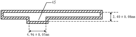
- the first face 40a of the female connector 40 is provided with a finite stop structure 45, and the stop structure 45 is a groove.
- the groove is indicated by an elliptical dotted line.
- the stop structure 45 i.e., the recess
- the first pin 41 is located in the middle of the first face 40a of the female connector 40.
- the middle portion means that the distance between the first pin 41 and the pin at both ends of the first face 40a of the female connector 40 is the same or similar, and does not define the first pin 41 and the first face 40a of the female connector 40.
- the distance between the pins of the two ends must be the same, i.e., the first pin 41 is not limited to be located in the middle of the first face 40a of the female connector 40.
- FIG. 8 another schematic view of the female connector 40 is shown.
- the female connector 40 is the female end of the SFF-8639 connector
- the first side 40a of the female connector 40 is provided with S1.
- S7 pin, E1 to E6 pin and P1 to P15 pin a total of 28 pins, the above 28 pins start from the first end of the female connector 40, according to the S1 to S7 pins, E1 to E6
- the order of the pins and the P1 to P15 pins are sequentially arranged one by one to the second end of the female connector 40; wherein the E1 to E6 pins are disposed at the groove positions, and the S1 to S7 pins are located at the grooves close to the above One side of the first end of the female connector 40, the P1 to P15 pins are located on the side of the recess adjacent to the second end of the female connector 40.
- the second side of the female connector 40 is provided with E7 to E16, S8 to S28 and E17 to E25 pins for a total of 40 pins, and the above 40 pins start from the first end of the female connector 40, according to The order of the E7 to E16, S8 to S28, and E17 to E25 pins is sequentially arranged one by one to the second end of the female connector 40.
- the P4 pin is used to indicate the in-position signal of the NVMe storage device, that is, the first pin 41 is the P4 pin.
- the first pin 41 (i.e., the P4 pin) is disposed on the first face 40a of the female connector 40, and the 17th pin counts from the first end of the female connector 40.
- the distance between the first pin 41 and the pin at both ends of the first face 40a of the female connector 40 is 17.87 mm and 13.97 mm, respectively. That is, as shown in FIG. 8, the distance between the first pin 41 (i.e., the P4 pin) and the first edge pin (i.e., the S1 pin) at one end of the first face 40a of the female connector 40. At 17.87 mm, the distance between the first pin 41 (i.e., the P4 pin) and the second edge pin (i.e., the P15 pin) at the other end of the first face 40a of the female connector 40 is 13.97 mm.
- the distance between the above two pins refers to the distance between the center line positions of the gold fingers of the two pins.
- the pins of the female connector 40 include a long needle and a short needle, and the long needle is longer than the short needle, and the length difference is greater than or equal to 0.35 mm.
- the distance between the long needle and the socket side edge of the female connector 40 is 1.40 ⁇ 0.15 mm
- the distance between the short needle and the slot side edge of the female connector 40 is 1.90 ⁇ 0.15 mm. That is, when the first pin 41 (ie, the P4 pin) is a short pin, the distance between the first pin 41 (ie, the P4 pin) and the slot side edge of the female connector 40 is 1.90. ⁇ 0.15mm.
- the first pin 41 (ie, the P4 pin) is a long pin, the distance between the first pin 41 (ie, the P4 pin) and the slot side edge of the female connector 40 is 1.40 ⁇ 0.15 mm. .
- the pin of the female connector 40 for indicating the signal of the in-position signal, the power signal, the clock signal and the PCIe port is used.
- the length is the same, or the length of the pin in the female connector 40 for indicating the in-position signal is not longer than the length of the pin for indicating the power signal, the clock signal, and the signal of the PCIe port, thereby enabling the in-position signal to be more
- the NVMe storage device avoids the problem of unsuccessful access to the system in the scenario of plugging and unplugging.
- FIG. 9 is a schematic diagram of a storage system according to an embodiment of the present application.
- the storage system includes an NVMe storage device 50 and a computer device 60.
- the NVMe storage device 50 is one or more.
- the NVMe storage device 50 can be an NVMe SSD.
- Computer device 60 may be a computer, a storage array (or array cabinet) or a server, and computer device 60 may be referred to as a host. At least one slot is formed in the computer device 60, and each slot is available for insertion into an NVMe storage device 50.
- the NVMe storage device 50 is interfacing with the computer device 60 through the connector provided by the above embodiments.
- the connector is in the "SFF-8639 Specification for Multifunction 12 Gb/s 6X Unshielded Connector", "PCI” SFF-8639 Module Specification and SFF-8639 connector as defined in the relevant standards such as 2012 SSD Form Factor Work Group, All rights reserved.
- the NVMe storage device 50 and the computer device 60 will be described separately.
- FIG. 10 is a structural block diagram of an NVMe storage device 50 according to an embodiment of the present application.
- the NVMe storage device 50 includes a controller 51, a memory 52, and a connector 53.
- the controller 51 is electrically connected to the memory 52 and the connector 53, respectively.
- the controller 51 is primarily responsible for data communication with the computer device 60 for reading data from or writing data to the memory 52 in accordance with read and write requests from the computer device 60.
- the controller 51 communicates with the computer device 60 via a PCIe bus.
- the memory 62 is used to store data. Alternatively, the memory 62 is a flash memory or a DRAM.
- the dimensions of the NVMe storage device 50 include, but are not limited to, 3.5 inches, 2.5 inches, and 1.8 inches.
- the connector 53 of the NVMe storage device 50 is a male connector, such as the male connector of the SFF-8639 connector.
- the male connector refer to the embodiment of FIG. 3 above, which is not described in this embodiment.
- the computer device 60 for insertion of the NVMe storage device 50 also includes a connector, and the connector 53 of the NVMe storage device 50 is plugged into the connector of the computer device 60.
- the connector 53 of the NVMe storage device 50 is a male connector and the connector of the computer device 60 is a female connector.
- the connector 53 of the NVMe storage device 50 is a female connector and the connector of the computer device 60 is a male connector, which is not limited in this embodiment of the present application.
- the contact order of the two pins is 1st, that is, the contact time of the two pins.
- the contact order of the two pins is 2nd, That is, the contact time is later than the contact time of the pin having the contact order of 1st;
- the two tubes are The contact order of the feet is 3rd, that is, the contact time is later than the contact time of the contacts in the contact order of 2nd.
- the connector 53 of the NVMe storage device 50 is a short pin
- the connector of the computer device 60 is used to indicate the first of the in-position signals.
- the contact order of the two first pins is 3rd.
- the pin of the connector for indicating the signal of the in-position signal, the power signal, the clock signal, and the PCIe port is changed by changing the length of the pin in the connector.
- the length is the same, or the length of the pin in the connector for indicating the in-position signal is not longer than the length of the pin for indicating the power signal, the clock signal, and the signal of the PCIe port, such as the male connector and the female connector.
- the first pin in the connector is changed from a long pin to a short pin, so that the contact order of the first pin is changed from 1st to 3rd. In both of the plug-and-play scenarios mentioned above, it is ensured that the NVMe storage device 50 successfully accesses the system. Specifically:
- the first pin that is, the P4 pin of the SFF-8639 connector
- the bit signal IFDET# changes from 1 to 0, indicating that the NVMe storage device 50 is in place.
- the system detects that the above-mentioned in-position signal IFDET# changes from 1 to 0, it reports the interrupt.
- the PCIe hot-swap controller in the system turns on the power, clock and PCIe port of the slot to start the hot add process. Since the power, clock, and PCIe port pins are already in contact at this time, the hot add process is successfully executed, so that the NVMe storage device 50 successfully accesses the system.
- the first pin that is, the P4 pin of the SFF-8639 connector
- the first pin is also disconnected, and the bit signal IFDET# will change from 0 to 1, indicating that the NVMe storage device 50 is not in place.
- the PCIe link is disconnected and the DPC is triggered, the NVMe storage device 50 is isolated and the PCIe port is closed.
- the bit signal IFDET# will change from 1 to 0, indicating that the NVMe storage device 50 is in place.
- the PCIe hot-swap controller in the system turns on the power, clock and PCIe port of the slot to start the hot add process. After the hot add process is completed, the NVMe storage device 50 re-enters the system.
- the length of the pin in the connector for indicating the signal of the in-position signal, the power signal, the clock signal, and the PCIe port is the same, or the connection is made.
- the length of the pin used to indicate the in-position signal is not longer than the length of the pin for indicating the power signal, the clock signal, and the signal of the PCIe port, so that the in-position signal can more accurately reflect the NVMe storage device. If the NVMe storage device is plugged or unplugged, the NVMe storage device cannot be successfully accessed.
- FIG. 11 is a structural block diagram of a computer device 60 according to an embodiment of the present application.
- Computer device 60 includes a processing module 61 and a connector 62.
- the processing module 61 is electrically connected to the connector 62.
- the processing module 61 is configured to control management of the actions of the computer device 60, such as sending read and write requests to the NVMe storage device 50 to request read data from or write data to the NVMe storage device 50.
- the processing module 61 communicates with the NVMe storage device 50 via a PCIe bus.
- the connector 62 of the computer device 60 is a female connector, such as the female of the SFF-8639 connector.
- the female connector refer to the embodiment of FIG. 6 above, which is not described in this embodiment.
- the NVMe storage device 50 plugged into the computer device 60 also includes a connector, and the connector of the NVMe storage device 50 is plugged into the connector 62 of the computer device 60.
- the connector of the NVMe storage device 50 is a male connector and the connector 62 of the computer device 60 is a female connector.
- the connector of the NVMe storage device 50 is a female connector and the connector 62 of the computer device 60 is a male connector, which is not limited in this embodiment of the present application.
- the contact order of the two pins is 1st; when the connector of the NVMe storage device 50 and When one of the two pins in the connector 62 of the computer device 60 is a long pin and the other is a short pin, the contact order of the two pins is 2nd; when the connector and computer device of the NVMe storage device 50 When the two pins in the connector 62 of 60 are short pins, the contact order of the two pins is 3rd.
- the contact order of the two first pins is 3rd.
- the pin of the connector for indicating the signal of the in-position signal, the power signal, the clock signal, and the PCIe port is changed by changing the length of the pin in the connector.
- the length is the same, or the length of the pin in the connector for indicating the in-position signal is not longer than the length of the pin for indicating the power signal, the clock signal, and the signal of the PCIe port, such as the male connector and the female connector.
- the first pin in the connector is changed from a long pin to a short pin, so that the contact order of the first pin is changed from 1st to 3rd. In both of the plug-and-play scenarios mentioned above, it is ensured that the NVMe storage device 50 successfully accesses the system.
- the NVMe storage device 50 successfully accesses the system.
- the processing module 61 includes a CPU 61a.
- the CPU 61a is electrically connected to the connector 62, for example, via a PCIe bus.
- the CPU 61a is used to control and manage the actions of the computer device 60, and its functions are mainly to interpret computer instructions and process data in the computer software.
- the processing module 61 includes a CPU 61a and a PCIe switch chip 61b.
- the PCIe switch chip 61b includes one input port and N output ports, and N is a positive integer.
- the CPU 61a is electrically connected to the input port, for example, via a PCIe bus.
- Each of the N output ports is for electrical connection with a connector 62, such as a PCIe bus. Due to the presence of the PCIe switch chip 61b, the CPU 61a is enabled to support simultaneous communication with a plurality of NVMe storage devices 50.
- the processing module 61 further includes a Baseboard Management Controller (BMC) and a Complex Programmable Logic Device (CPLD).
- BMC Baseboard Management Controller
- CPLD Complex Programmable Logic Device
- the BMC and the CPLD are mainly used to assist the management of the power, clock, and in-position signals of the NVMe storage device 50. If the functions of the above BMC and CPLD are integrated in the CPU 61a or the PCIe switch chip 61b, the BMC and the CPLD can be omitted.
- the length of the pin in the connector for indicating the signal of the in-position signal, the power signal, the clock signal, and the PCIe port is the same, or the connection is made.
- the length of the pin used to indicate the in-position signal is not longer than the length of the pin for indicating the power signal, the clock signal, and the signal of the PCIe port, so that the in-position signal can more accurately reflect the NVMe storage device. If the NVMe storage device is plugged or unplugged, the NVMe storage device cannot be successfully accessed.
- the P4 pin For the short pin, and the pin used to indicate the in-position signal (that is, the P4 pin) is also changed from the long pin to the short pin in the SFF-8639 connector included in the computer device, the above two P4 pins are The contact sequence is 3rd, which avoids the problem that the system cannot be successfully accessed in the plugged-in scenario.
- the P4 pin in the SFF-8639 connector included in the NVMe storage device may also be changed from a long pin to a short pin, and the P4 tube in the SFF-8639 connector included in the computer device.
- the foot is still a long needle; or, the P4 pin in the SFF-8639 connector included in the computer device is changed from a long pin to a short pin, and the P4 pin in the SFF-8639 connector included in the NVMe storage device is still In the case of a long needle, the contact order of the two P4 pins is 2nd. In the scenario of plugging and unplugging, the problem that the system cannot be successfully accessed can be reduced to some extent compared with the prior art.
- the following software is included: device management driver, PCIe driver, and NVMe driver.
- the device management driver is mainly used for reporting the in-position signal and supporting data transfer between the underlying hardware and the PCIe driver.
- the PCIe driver is primarily used to perform hot-swap processes (including hot-add processes and hot-removal processes).
- the NVMe driver is primarily used to support the normal operation of the NVMe storage device 50.
- the above software can be stored in the memory of the computer device 60, loaded and executed by the CPU 61a.
- the lengths of the pins for indicating the signals of the bit signal, the power signal, the clock signal, and the PCIe port in the connector are adjusted to be the same by the embodiment of FIG. 14 and FIG. 15, or the connector is used for the indication.
- the length of the pin of the bit signal is adjusted to be longer than the length of the pin for indicating the power signal, the clock signal, and the signal of the PCIe port, the corresponding hot add process and the heat removal process are separately described.
- FIG. 14 shows a schematic diagram of a hot addition process.
- the hot addition process can include the following steps:
- Step 1401 the underlying hardware sends an interrupt when it detects that the NVMe storage device 50 is inserted into the slot.
- the underlying hardware detects that the in-position signal IFDET# changes from 1 to 0, it indicates that the NVMe storage device 50 is inserted into the slot and issues an interrupt.
- Step 1402 the underlying hardware sends a hot add event to the device management driver.
- Step 1403 the device management driver lights up the hot plug indicator
- Step 1404 the device management driver sends a hot add event to the PCIe driver.
- the device management driver detects whether the hot add event is legal; if it is legal, performs steps 1403 and 1404; if not, ends the process.
- step 1403 may be performed before step 1404, or may be performed after step 1404, or may be performed simultaneously with step 1404, which is not limited by the embodiment of the present application.
- Step 1405 After receiving the hot add event, the PCIe driver sends a power up notification to the device management driver.
- the power-on notification is used to inform the device management driver that the PCIe driver powers up the slot in which the NVMe storage device 50 is inserted.
- Step 1406 the PCIe driver powers up the slot inserted by the NVMe storage device 50 through a board support package (BSP);
- BSP board support package
- the underlying hardware illuminates the power light of the slot in which the NVMe storage device 50 is inserted.
- step 1405 may be performed before the step 1406, or may be performed after the step 1406, or may be performed simultaneously with the step 1406, which is not limited by the embodiment of the present application.
- Step 1407 The PCIe driver detects a link state, where the link state is used to indicate whether the PCIe link is successfully established.
- the PCIe driver polls the underlying hardware for link status.
- the duration of the polling process may be preset according to actual needs, for example, 2 seconds; or the number of pollings of the polling process may be preset according to actual needs, for example, 3 times.
- the above resources include a memory address space.
- Step 1409 the PCIe driver invokes the NVMe driver.
- Step 1410 the NVMe driver initializes the NVMe storage device 50 after being invoked
- the capacity, partition, and the like of the NVMe storage device 50 are initialized.
- step 1411 the PCIe driver starts the Advanced Error Reporting (AER) function, and the hot add process ends.
- AER Advanced Error Reporting
- FIG. 15 shows a schematic diagram of a heat removal process.
- the hot removal process can include the following steps:
- Step 1501 When the bottom hardware detects that the NVMe storage device 50 is unplugged from the slot, the DPC interrupt is issued, and the NVMe storage device 50 is controlled to enter the isolated state.
- the underlying hardware detects that the in-position signal IFDET# changes from 0 to 1, or when it detects that the PCIe link is disconnected, it indicates that the NVMe storage device 50 is unplugged from the slot and issues a DPC interrupt.
- the lengths of the pins in the connector for indicating the signals of the bit signal, the power signal, the clock signal and the PCIe port are adjusted to be the same, or the connector is used to indicate the in-position signal.
- the length of the pin is adjusted to be longer than the length of the pin for indicating the power signal, the clock signal, and the signal of the PCIe port.
- the bit signal changes and PCIe The link disconnection occurs substantially simultaneously, or the bit signal changes before the PCIe link is disconnected.
- the underlying hardware can detect NVMe storage by detecting any of the above events (ie, the bit signal changes or the PCIe link is disconnected). Device 50 is pulled out of the slot.
- the purpose of controlling the NVMe storage device 50 to enter the isolation state is to protect the system from being affected by the hot removal event, and to avoid abnormal errors such as timeout and hang.
- Step 1502 the underlying hardware sends a DPC event to the PCIe driver.
- Step 1503 the PCIe driver turns off the AER function, and clears the AER error of the port corresponding to the NVMe storage device 50;
- the PCIe driver detects whether the DPC event is legal; if it is legal, the AER function is disabled; if not, the process ends.
- Step 1504 the PCIe driver sends a service interruption notification to the NVMe driver.
- Step 1505 After receiving the service interruption notification, the NVMe driver stops running the service.
- Step 1506 the PCIe driver releases the isolation state after confirming that the service packet has been cleared.
- Step 1507 the PCIe driver detects the link status.
- the PCIe driver polls the underlying hardware for link status.
- the duration of the polling process may be preset according to actual needs, for example, 2 seconds; or the number of pollings of the polling process may be preset according to actual needs, for example, 3 times.
- Step 1508 the PCIe driver sends a hot removal event to the device management driver after determining that the link cannot be reestablished;
- Step 1509 After the device management driver receives the hot removal event, the hot plug indicator is illuminated
- Step 1510 The device management driver sends a hot removal confirmation event to the PCIe driver.
- Step 1511 After receiving the hot removal confirmation event, the PCIe driver sends a power-off notification to the device management driver.
- the power-off notification is used to inform the device management driver that the PCIe driver powers down the slot in which the NVMe storage device 50 is inserted.
- Step 1512 the PCIe driver removes the NVMe storage device 50
- Step 1513 the PCIe driver deletes the resources of the NVMe storage device 50.
- the above resources include a memory address space.
- Step 1514 the PCIe driver invokes the NVMe driver
- Step 1515 the NVMe driver removes the NVMe storage device 50 after being invoked
- step 1516 the PCIe driver powers down the slot inserted by the NVMe storage device 50 through the BSP.
- the underlying hardware extinguishes the power light of the slot in which the NVMe storage device 50 is inserted.
- Step 1517 The PCIe driver sends a power-off completion event to the device management driver.
- step 1518 the device management driver turns off the hot plug indicator, and the hot removal process ends.
- a plurality as referred to herein means two or more.
- "and/or” describing the association relationship of the associated objects, indicating that there may be three relationships, for example, A and/or B, which may indicate that there are three cases where A exists separately, A and B exist at the same time, and B exists separately.
- the character “/” generally indicates that the contextual object is an "or” relationship.
- the words “first,” “second,” and similar terms used herein do not denote any order, quantity, or importance, but are merely used to distinguish different objects.
Landscapes
- Engineering & Computer Science (AREA)
- Theoretical Computer Science (AREA)
- General Engineering & Computer Science (AREA)
- Physics & Mathematics (AREA)
- General Physics & Mathematics (AREA)
- Computer Hardware Design (AREA)
- Human Computer Interaction (AREA)
- Details Of Connecting Devices For Male And Female Coupling (AREA)
- Power Sources (AREA)
Abstract
L'invention concerne un connecteur (53), un dispositif de stockage NVMe (50) et un dispositif informatique (60). Le connecteur (53) comprend une première broche (31), une deuxième broche (32), une troisième broche (33) et une quatrième broche (34). La première broche (31) est utilisée pour indiquer un signal de bit (31); la deuxième broche (32) est utilisée pour indiquer un signal de puissance ; la troisième broche (33) est utilisée pour indiquer un signal d'horloge ; et la quatrième broche (34) est utilisée pour indiquer un signal d'une interface PCIe. La première broche (31), la deuxième broche (32), la troisième broche (33) et la quatrième broche (34) ont la même longueur. Le connecteur (53) comprend un premier côté (30a) et un second côté, le premier côté (30a) étant pourvu d'une structure de retenue (35); la structure de retenue (35) est constituée d'une bosse ou d'un évidement ; la première broche (31) est au milieu du premier côté (30a). Comme la longueur de la broche indiquant un signal de bit dans le connecteur (53) n'est pas plus grande que la longueur des broches indiquant la puissance, l'horloge et les signaux d'interface PCIe, le signal de bit peut refléter avec précision l'état de branchement ou de débranchement du dispositif de stockage NVMe (50), ce qui permet d'éviter le problème de défaillance d'accès au système lorsque le dispositif de stockage NVMe (50) se trouve dans les scènes de branchement et de débranchement.
Priority Applications (3)
| Application Number | Priority Date | Filing Date | Title |
|---|---|---|---|
| EP18866541.8A EP3674906B1 (fr) | 2017-10-13 | 2018-02-06 | Connecteur, dispositif de stockage nvme et dispositif informatique |
| CN201880000286.XA CN108323217B (zh) | 2017-10-13 | 2018-02-06 | 连接器、NVMe存储设备及计算机设备 |
| US16/839,476 US11822498B2 (en) | 2017-10-13 | 2020-04-03 | Connector, NVMe storage device, and computer device |
Applications Claiming Priority (2)
| Application Number | Priority Date | Filing Date | Title |
|---|---|---|---|
| CN201721329936.4U CN207529373U (zh) | 2017-10-13 | 2017-10-13 | 连接器、NVMe存储设备及计算机设备 |
| CN201721329936.4 | 2017-10-13 |
Related Child Applications (1)
| Application Number | Title | Priority Date | Filing Date |
|---|---|---|---|
| US16/839,476 Continuation US11822498B2 (en) | 2017-10-13 | 2020-04-03 | Connector, NVMe storage device, and computer device |
Publications (1)
| Publication Number | Publication Date |
|---|---|
| WO2019071887A1 true WO2019071887A1 (fr) | 2019-04-18 |
Family
ID=62569944
Family Applications (1)
| Application Number | Title | Priority Date | Filing Date |
|---|---|---|---|
| PCT/CN2018/075438 WO2019071887A1 (fr) | 2017-10-13 | 2018-02-06 | Connecteur, dispositif de stockage nvme et dispositif informatique |
Country Status (4)
| Country | Link |
|---|---|
| US (1) | US11822498B2 (fr) |
| EP (1) | EP3674906B1 (fr) |
| CN (1) | CN207529373U (fr) |
| WO (1) | WO2019071887A1 (fr) |
Families Citing this family (9)
| Publication number | Priority date | Publication date | Assignee | Title |
|---|---|---|---|---|
| CN108323217B (zh) * | 2017-10-13 | 2020-11-06 | 华为技术有限公司 | 连接器、NVMe存储设备及计算机设备 |
| CN207529373U (zh) | 2017-10-13 | 2018-06-22 | 华为技术有限公司 | 连接器、NVMe存储设备及计算机设备 |
| US11163348B2 (en) * | 2018-05-03 | 2021-11-02 | Samsung Electronics Co., Ltd. | Connectors that connect a storage device and power supply control device, and related power supply control devices and host interface devices |
| CN109933495A (zh) * | 2018-12-13 | 2019-06-25 | 英业达科技有限公司 | 检测控制电路及检测控制方法 |
| CN111244698B (zh) * | 2020-01-08 | 2021-12-21 | 富鼎精密工业(郑州)有限公司 | 电连接器 |
| CN111769396B (zh) * | 2020-07-24 | 2021-10-26 | 东莞立讯技术有限公司 | 端子结构和电连接器 |
| US20220200867A1 (en) * | 2020-12-18 | 2022-06-23 | Western Digital Technologies, Inc. | Management of non-volatile memory express nodes |
| CN214957657U (zh) * | 2021-04-23 | 2021-11-30 | 东莞富强电子有限公司 | 高速连接器 |
| CN116932311A (zh) * | 2022-03-29 | 2023-10-24 | 富联精密电子(天津)有限公司 | 固态硬盘状态监控方法、系统、服务器及存储介质 |
Citations (5)
| Publication number | Priority date | Publication date | Assignee | Title |
|---|---|---|---|---|
| CN1731362A (zh) * | 2005-08-24 | 2006-02-08 | 杭州华为三康技术有限公司 | 硬盘热插拔保护系统及方法 |
| CN101201888A (zh) * | 2006-12-14 | 2008-06-18 | 华为技术有限公司 | 一种减少cf卡损坏的方法及装置 |
| CN105095037A (zh) * | 2015-09-11 | 2015-11-25 | 北京星网锐捷网络技术有限公司 | 线卡、线卡的背板以及线卡测试方法 |
| CN105893298A (zh) * | 2016-06-29 | 2016-08-24 | 联想(北京)有限公司 | 一种接口连接方法及电子设备 |
| US9703745B2 (en) * | 2013-07-15 | 2017-07-11 | Hong Fu Jin Industry (Shenzhen) Co., Ltd. | Storage device and motherboard able to support the storage device |
Family Cites Families (14)
| Publication number | Priority date | Publication date | Assignee | Title |
|---|---|---|---|---|
| US7497709B1 (en) | 2007-09-12 | 2009-03-03 | Hon Hai Precision Ind. Co., Ltd. | Electrical connector with switch device |
| EP2096527A1 (fr) | 2008-02-28 | 2009-09-02 | Dotop Technology, Inc. | Disque à l'état solide |
| US8342886B2 (en) | 2011-03-14 | 2013-01-01 | Hon Hai Precision Ind. Co., Ltd. | Electrical connector with connecting bars therein to reduce cross talking |
| CN104035341A (zh) | 2013-03-05 | 2014-09-10 | 李文庆 | 一种家电的外挂式控制机构 |
| US9927851B2 (en) * | 2014-11-26 | 2018-03-27 | Hewlett Packard Enterprise Development Lp | Storage drive carrier module |
| US9768640B2 (en) * | 2014-12-19 | 2017-09-19 | Kabushiki Kaisha Toshiba | Switching the power supply source of system to one of a first battery in electronic apparatus and a second battery in extension detachable and attachable to the apparatus |
| CN104951384B (zh) * | 2015-06-16 | 2017-10-03 | 浪潮电子信息产业股份有限公司 | 一种基于nvme ssd硬盘的监控系统、基板管理控制器和监控方法 |
| US10255215B2 (en) * | 2016-01-29 | 2019-04-09 | Liqid Inc. | Enhanced PCIe storage device form factors |
| CN106407146B (zh) | 2016-09-09 | 2019-04-16 | 广州视源电子科技股份有限公司 | 一种接口设备、安全接入的方法及装置 |
| CN206236840U (zh) | 2016-12-01 | 2017-06-09 | 深圳市胜航精密连接器有限公司 | 一种新型带led支架的sff‑8639连接器 |
| US10198385B2 (en) * | 2017-03-13 | 2019-02-05 | American Megatrends, Inc. | System and method for detecting types of storage drives connected to backplane controller or enclosure management controller |
| CN107145430A (zh) * | 2017-04-21 | 2017-09-08 | 深圳市同泰怡信息技术有限公司 | 一种基于I2C接口通过CPLD来实现NVMe SSD点灯的方法 |
| CN107220196A (zh) * | 2017-05-27 | 2017-09-29 | 郑州云海信息技术有限公司 | 一种支持Tri‑Mode的内置高端存储卡 |
| CN207529373U (zh) | 2017-10-13 | 2018-06-22 | 华为技术有限公司 | 连接器、NVMe存储设备及计算机设备 |
-
2017
- 2017-10-13 CN CN201721329936.4U patent/CN207529373U/zh active Active
-
2018
- 2018-02-06 EP EP18866541.8A patent/EP3674906B1/fr active Active
- 2018-02-06 WO PCT/CN2018/075438 patent/WO2019071887A1/fr unknown
-
2020
- 2020-04-03 US US16/839,476 patent/US11822498B2/en active Active
Patent Citations (5)
| Publication number | Priority date | Publication date | Assignee | Title |
|---|---|---|---|---|
| CN1731362A (zh) * | 2005-08-24 | 2006-02-08 | 杭州华为三康技术有限公司 | 硬盘热插拔保护系统及方法 |
| CN101201888A (zh) * | 2006-12-14 | 2008-06-18 | 华为技术有限公司 | 一种减少cf卡损坏的方法及装置 |
| US9703745B2 (en) * | 2013-07-15 | 2017-07-11 | Hong Fu Jin Industry (Shenzhen) Co., Ltd. | Storage device and motherboard able to support the storage device |
| CN105095037A (zh) * | 2015-09-11 | 2015-11-25 | 北京星网锐捷网络技术有限公司 | 线卡、线卡的背板以及线卡测试方法 |
| CN105893298A (zh) * | 2016-06-29 | 2016-08-24 | 联想(北京)有限公司 | 一种接口连接方法及电子设备 |
Non-Patent Citations (1)
| Title |
|---|
| See also references of EP3674906A4 * |
Also Published As
| Publication number | Publication date |
|---|---|
| US11822498B2 (en) | 2023-11-21 |
| EP3674906A4 (fr) | 2020-10-07 |
| US20200233823A1 (en) | 2020-07-23 |
| EP3674906A1 (fr) | 2020-07-01 |
| EP3674906B1 (fr) | 2021-09-29 |
| CN207529373U (zh) | 2018-06-22 |
Similar Documents
| Publication | Publication Date | Title |
|---|---|---|
| WO2019071887A1 (fr) | Connecteur, dispositif de stockage nvme et dispositif informatique | |
| US11567895B2 (en) | Method, apparatus and system for dynamic control of clock signaling on a bus | |
| US20120042178A1 (en) | Peripheral Device | |
| JP2008511916A (ja) | ハブ機能付きメモリデバイス | |
| US10853289B2 (en) | System, apparatus and method for hardware-based bi-directional communication via reliable high performance half-duplex link | |
| US20130339552A1 (en) | Active cable management | |
| US20050015655A1 (en) | Intermediate station | |
| JP2018536239A (ja) | ユニバーサルシリアルバス(usb)ケーブルにおけるデータフローの増大 | |
| US9287669B2 (en) | SATA express connector | |
| CN108170620A (zh) | 一种服务器用硬盘拓展系统及方法、硬盘信号增强方法 | |
| US11232060B2 (en) | Method, apparatus and system for power supply policy exchange on a bus | |
| US20150026503A1 (en) | Appliances powered over sas | |
| CN102339236B (zh) | 侦测可插拔储存装置的方法及电子装置 | |
| JP3140192U (ja) | E−sata信号と電力を伝送する伝送ケーブル | |
| US8583966B2 (en) | Methods and structure for debugging DDR memory of a storage controller | |
| CN108323217B (zh) | 连接器、NVMe存储设备及计算机设备 | |
| US20230418703A1 (en) | Autonomic troubleshooting of a system of devices | |
| WO2012048598A1 (fr) | Carte express à mémoire mobile et ordinateur | |
| US7613879B2 (en) | Method, system and media for improved operation of a device in a foreign domain | |
| JP2013047994A (ja) | 周辺機器、及び、ホスト機器と周辺機器の接続方法 | |
| WO2020014836A1 (fr) | Procédé, dispositif et système d'acquisition d'informations de négociation de liaison d'un module optique | |
| US10817436B2 (en) | Removal warning for connectable devices | |
| US20060047934A1 (en) | Integrated circuit capable of memory access control | |
| TWI541656B (zh) | SATA Express interface storage device and its inserted motherboard | |
| CN103365811A (zh) | 电子装置和主机确定方法 |
Legal Events
| Date | Code | Title | Description |
|---|---|---|---|
| 121 | Ep: the epo has been informed by wipo that ep was designated in this application |
Ref document number: 18866541 Country of ref document: EP Kind code of ref document: A1 |
|
| ENP | Entry into the national phase |
Ref document number: 2018866541 Country of ref document: EP Effective date: 20200327 |
|
| NENP | Non-entry into the national phase |
Ref country code: DE |