WO2019064374A1 - 表示パネルの製造方法、表示パネルの製造装置 - Google Patents
表示パネルの製造方法、表示パネルの製造装置 Download PDFInfo
- Publication number
- WO2019064374A1 WO2019064374A1 PCT/JP2017/034939 JP2017034939W WO2019064374A1 WO 2019064374 A1 WO2019064374 A1 WO 2019064374A1 JP 2017034939 W JP2017034939 W JP 2017034939W WO 2019064374 A1 WO2019064374 A1 WO 2019064374A1
- Authority
- WO
- WIPO (PCT)
- Prior art keywords
- manufacturing
- display panel
- inspection
- mother substrate
- correction value
- Prior art date
- Legal status (The legal status is an assumption and is not a legal conclusion. Google has not performed a legal analysis and makes no representation as to the accuracy of the status listed.)
- Ceased
Links
Images




Classifications
-
- G—PHYSICS
- G09—EDUCATION; CRYPTOGRAPHY; DISPLAY; ADVERTISING; SEALS
- G09G—ARRANGEMENTS OR CIRCUITS FOR CONTROL OF INDICATING DEVICES USING STATIC MEANS TO PRESENT VARIABLE INFORMATION
- G09G3/00—Control arrangements or circuits, of interest only in connection with visual indicators other than cathode-ray tubes
- G09G3/20—Control arrangements or circuits, of interest only in connection with visual indicators other than cathode-ray tubes for presentation of an assembly of a number of characters, e.g. a page, by composing the assembly by combination of individual elements arranged in a matrix no fixed position being assigned to or needed to be assigned to the individual characters or partial characters
- G09G3/22—Control arrangements or circuits, of interest only in connection with visual indicators other than cathode-ray tubes for presentation of an assembly of a number of characters, e.g. a page, by composing the assembly by combination of individual elements arranged in a matrix no fixed position being assigned to or needed to be assigned to the individual characters or partial characters using controlled light sources
- G09G3/30—Control arrangements or circuits, of interest only in connection with visual indicators other than cathode-ray tubes for presentation of an assembly of a number of characters, e.g. a page, by composing the assembly by combination of individual elements arranged in a matrix no fixed position being assigned to or needed to be assigned to the individual characters or partial characters using controlled light sources using electroluminescent panels
- G09G3/32—Control arrangements or circuits, of interest only in connection with visual indicators other than cathode-ray tubes for presentation of an assembly of a number of characters, e.g. a page, by composing the assembly by combination of individual elements arranged in a matrix no fixed position being assigned to or needed to be assigned to the individual characters or partial characters using controlled light sources using electroluminescent panels semiconductive, e.g. using light-emitting diodes [LED]
- G09G3/3208—Control arrangements or circuits, of interest only in connection with visual indicators other than cathode-ray tubes for presentation of an assembly of a number of characters, e.g. a page, by composing the assembly by combination of individual elements arranged in a matrix no fixed position being assigned to or needed to be assigned to the individual characters or partial characters using controlled light sources using electroluminescent panels semiconductive, e.g. using light-emitting diodes [LED] organic, e.g. using organic light-emitting diodes [OLED]
-
- G—PHYSICS
- G09—EDUCATION; CRYPTOGRAPHY; DISPLAY; ADVERTISING; SEALS
- G09F—DISPLAYING; ADVERTISING; SIGNS; LABELS OR NAME-PLATES; SEALS
- G09F9/00—Indicating arrangements for variable information in which the information is built-up on a support by selection or combination of individual elements
-
- H—ELECTRICITY
- H10—SEMICONDUCTOR DEVICES; ELECTRIC SOLID-STATE DEVICES NOT OTHERWISE PROVIDED FOR
- H10K—ORGANIC ELECTRIC SOLID-STATE DEVICES
- H10K71/00—Manufacture or treatment specially adapted for the organic devices covered by this subclass
- H10K71/70—Testing, e.g. accelerated lifetime tests
-
- H—ELECTRICITY
- H10—SEMICONDUCTOR DEVICES; ELECTRIC SOLID-STATE DEVICES NOT OTHERWISE PROVIDED FOR
- H10P—GENERIC PROCESSES OR APPARATUS FOR THE MANUFACTURE OR TREATMENT OF DEVICES COVERED BY CLASS H10
- H10P74/00—Testing or measuring during manufacture or treatment of wafers, substrates or devices
- H10P74/20—Testing or measuring during manufacture or treatment of wafers, substrates or devices characterised by the properties tested or measured, e.g. structural or electrical properties
- H10P74/203—Structural properties, e.g. testing or measuring thicknesses, line widths, warpage, bond strengths or physical defects
-
- G—PHYSICS
- G02—OPTICS
- G02F—OPTICAL DEVICES OR ARRANGEMENTS FOR THE CONTROL OF LIGHT BY MODIFICATION OF THE OPTICAL PROPERTIES OF THE MEDIA OF THE ELEMENTS INVOLVED THEREIN; NON-LINEAR OPTICS; FREQUENCY-CHANGING OF LIGHT; OPTICAL LOGIC ELEMENTS; OPTICAL ANALOGUE/DIGITAL CONVERTERS
- G02F1/00—Devices or arrangements for the control of the intensity, colour, phase, polarisation or direction of light arriving from an independent light source, e.g. switching, gating or modulating; Non-linear optics
- G02F1/01—Devices or arrangements for the control of the intensity, colour, phase, polarisation or direction of light arriving from an independent light source, e.g. switching, gating or modulating; Non-linear optics for the control of the intensity, phase, polarisation or colour
- G02F1/13—Devices or arrangements for the control of the intensity, colour, phase, polarisation or direction of light arriving from an independent light source, e.g. switching, gating or modulating; Non-linear optics for the control of the intensity, phase, polarisation or colour based on liquid crystals, e.g. single liquid crystal display cells
- G02F1/1306—Details
- G02F1/1309—Repairing; Testing
-
- G—PHYSICS
- G02—OPTICS
- G02F—OPTICAL DEVICES OR ARRANGEMENTS FOR THE CONTROL OF LIGHT BY MODIFICATION OF THE OPTICAL PROPERTIES OF THE MEDIA OF THE ELEMENTS INVOLVED THEREIN; NON-LINEAR OPTICS; FREQUENCY-CHANGING OF LIGHT; OPTICAL LOGIC ELEMENTS; OPTICAL ANALOGUE/DIGITAL CONVERTERS
- G02F1/00—Devices or arrangements for the control of the intensity, colour, phase, polarisation or direction of light arriving from an independent light source, e.g. switching, gating or modulating; Non-linear optics
- G02F1/01—Devices or arrangements for the control of the intensity, colour, phase, polarisation or direction of light arriving from an independent light source, e.g. switching, gating or modulating; Non-linear optics for the control of the intensity, phase, polarisation or colour
- G02F1/13—Devices or arrangements for the control of the intensity, colour, phase, polarisation or direction of light arriving from an independent light source, e.g. switching, gating or modulating; Non-linear optics for the control of the intensity, phase, polarisation or colour based on liquid crystals, e.g. single liquid crystal display cells
- G02F1/133—Constructional arrangements; Operation of liquid crystal cells; Circuit arrangements
- G02F1/1333—Constructional arrangements; Manufacturing methods
- G02F1/133351—Manufacturing of individual cells out of a plurality of cells, e.g. by dicing
-
- G—PHYSICS
- G09—EDUCATION; CRYPTOGRAPHY; DISPLAY; ADVERTISING; SEALS
- G09G—ARRANGEMENTS OR CIRCUITS FOR CONTROL OF INDICATING DEVICES USING STATIC MEANS TO PRESENT VARIABLE INFORMATION
- G09G2320/00—Control of display operating conditions
- G09G2320/02—Improving the quality of display appearance
- G09G2320/029—Improving the quality of display appearance by monitoring one or more pixels in the display panel, e.g. by monitoring a fixed reference pixel
- G09G2320/0295—Improving the quality of display appearance by monitoring one or more pixels in the display panel, e.g. by monitoring a fixed reference pixel by monitoring each display pixel
Definitions
- the present invention relates to a method of manufacturing a display panel provided with a light emitting element, and a manufacturing apparatus of the display panel.
- Patent Document 1 describes an inspection method of an organic EL panel for manufacturing an organic EL panel in which unevenness of light emission intensity between organic EL elements in the panel is reduced.
- each panel when forming a plurality of display panels on one mother substrate in one slot, each panel is formed on the same mother substrate due to a difference in film thickness between the display panels, etc.
- the light emission intensity may be uneven. Such luminance unevenness tends to occur in the same distribution for each mother substrate included in the same lot.
- a method of manufacturing a display panel includes a plurality of inspection mother substrate manufacturing steps for manufacturing an inspection mother substrate including a plurality of inspection elements, and a plurality of display panels including light emitting elements.
- the manufacturing mother substrate manufacturing process for manufacturing the manufacturing mother substrate, the measurement process for measuring the distribution of the light emission intensity from the plurality of test elements, and the correction value of the light emission voltage for each display panel according to the distribution And a correction step of correcting the light emission voltage of the light emitting element of each of the display panels based on the correction value.
- a display panel manufacturing apparatus includes an inspection mother substrate including a plurality of inspection elements, and a plurality of manufacturing mother substrates including a plurality of display panels including light emitting elements.
- a correction value of the light emission voltage of the light emitting element for each display panel is calculated according to the distribution, and a substrate manufacturing apparatus to be manufactured, a measuring apparatus for measuring the distribution of light emission intensity from the plurality of inspection elements, A storage device for storing a correction value and recording the correction value on each of the display panels is provided.
- FIG. 5 is a flowchart showing a method of manufacturing an organic EL panel according to Embodiment 1.
- FIG. 2 is a schematic view showing an organic EL panel manufactured in Embodiment 1 and a manufacturing apparatus of the organic EL panel.
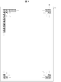
- FIG. 2 is a schematic top view showing an inspection mother substrate according to Embodiment 1.
- 1 is a schematic view showing a test element according to Embodiment 1.
- FIG. 1 is a schematic top view showing an organic EL panel according to Embodiment 1. It is a schematic top view which shows the positional relationship of the test
- FIG. 8 is a schematic view showing an organic EL panel manufactured in Embodiment 2 and a manufacturing apparatus of the organic EL panel.
- 7 is a flowchart showing a method of manufacturing an organic EL panel according to Embodiment 3.
- FIG. 10 is a schematic view showing an organic EL panel manufactured in Embodiment 3 and a manufacturing apparatus of the organic EL panel.
- FIG. 18 is a transparent top view for describing the positional relationship between the organic EL panel manufactured in Embodiment 3 and the corresponding inspection element. It is the schematic which shows the organic electroluminescent panel manufactured in a modification, and the manufacturing apparatus of the said organic electroluminescent panel.
- Embodiment 1 The method and apparatus for manufacturing the organic EL panel (display panel) according to the present embodiment will be described with reference to FIGS. 1 and 2 to 6.
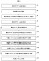
- FIG. 1 is a flowchart showing a method of manufacturing an organic EL panel according to the present embodiment.
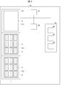
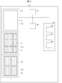
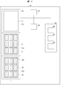
- FIG. 2 is a view for explaining an organic EL panel manufactured in the present embodiment and an apparatus for manufacturing the organic EL panel.
- the organic EL panel manufacturing apparatus 50 includes a control unit 52, a substrate manufacturing apparatus 54, a measuring apparatus 56, and a storage device 58.
- the storage device 58 includes a distribution storage device 60, a substrate information storage device 62, and a correction value storage device 64.
- the control unit 52 controls the substrate manufacturing device 54, the measuring device 56, and the storage device 58, respectively.
- the substrate manufacturing apparatus 54 includes a plurality of slots. In the present embodiment, the substrate manufacturing apparatus 54 manufactures the inspection mother substrate 4 in the first slot SL1. In addition, the substrate manufacturing apparatus 54 manufactures one manufacturing mother substrate 6 in each of the slots after the first slot SL1.
- FIG. 2 shows a first slot SL1, a second slot SL2, and a third slot SL3.
- the present invention is not limited to this, and the substrate manufacturing apparatus 54 may have more slots.
- the inspection mother substrate 4 is manufactured by the substrate manufacturing apparatus 54 (step S2). As shown in FIG. 3, the inspection mother substrate 4 includes a plurality of inspection elements 30 formed in a matrix on the mother glass substrate.
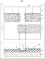
- FIG. 4 is a schematic view showing the inspection element 30 in detail
- FIG. 4 (a) is a top view
- FIG. 4 (b) is a schematic view showing a cross section along line AA 'in FIG. 4 (a). is there.
- the inspection element 30 includes a glass substrate 32, a reflective electrode 34, a transmissive electrode 36, a light emitting layer 38, and an insulating layer 40.
- the insulating layer 40 is omitted.
- the inspection element 30 has a plurality of sub-elements formed on a glass substrate 32.
- the sub-elements each include a reflective electrode 34, a transmissive electrode 36, and a light emitting layer 38 containing an organic EL.
- the electrodes of the subelements and the light emitting layer are respectively insulated by the insulating layer 40.
- the light emitting layer 38 emits light by applying an appropriate potential difference between the reflective electrode 34 and the transmissive electrode 36 of one subelement. At this time, the light from the light emitting layer 38 is reflected by the reflective electrode 34 and is transmitted through the transmissive electrode 36, and thus, travels toward the transmissive electrode 36 as shown by the arrow in FIG. 4B.
- the light emitted from the light emitting layer 38 of each sub element corresponds to the light emitted from each of the plurality of sub pixels in the light emitting element of the organic EL panel 8.
- the inspection mother substrate 4 is formed in the same process as the manufacture of the manufacturing mother substrate 6, with the configuration provided with the organic EL panel 8 of the manufacturing mother substrate 6 above the light emitting elements above the inspection element 30. Ru.
- the upper side of the inspection element 30 of the inspection mother substrate 4 has a configuration corresponding to the upper side of the light emitting element of the manufacturing mother substrate 6.
- the organic EL panel 8 may have a sealing film above the light emitting element, and in this case, a sealing film is similarly formed above the inspection element 30 of the inspection mother substrate 4. .
- the test elements 30 of the test mother substrate 4 are caused to emit light individually, and the light emission intensity is measured (step S 4).
- the distribution of the light emission intensity of the test element 30 is determined.
- the above measurement is performed by the measuring device 56.
- the measuring device 56 may employ various light intensity measuring devices known in the prior art.
- the inspection mother substrate 4 has unevenness in thickness
- the emission intensity from the inspection element 30 is relatively low at the thick position of the sealing film, and at the thin position of the sealing film, the inspection element 30 The emission intensity is relatively high.
- the thickness unevenness is similarly reflected on the manufacturing mother substrate 6. For this reason, when the light emitting element is caused to emit light by giving the same potential difference between the organic EL panels 8 on the manufacturing mother substrate 6, the luminance unevenness caused by the thickness unevenness is reflected.
- the distribution data of the necessary light emission voltage on the inspection mother substrate 4 is calculated from the measurement of the light emission intensity of the inspection element 30 described above (step S6).
- the distribution data of the necessary light emission voltage is recorded in the distribution storage device 60 of the storage device 58.
- the distribution data is determined from the relationship between the film thickness distribution of the manufacturing mother substrate 6 and the light emission intensity of the inspection element 30. For example, the distribution of the film thickness of the inspection mother substrate 4 manufactured in advance is measured, and the distribution of the light emission intensity of the inspection element 30 on the inspection mother substrate 4 is determined. Thus, the relationship between the film thickness of the inspection mother substrate 4 and the light emission intensity of the inspection element 30 can be obtained.
- the mother substrate 6 for manufacturing is made as a trial, and the light emission intensity of the inspection element 30 of the mother substrate 4 for inspection and the light emission intensity of the light emitting element of the mother substrate 6 for manufacturing are obtained Can calculate the relationship of From this, the necessary voltage for obtaining sufficient light emission from the light emitting element of the organic EL panel 8 of the actual manufacturing mother substrate 6 can be calculated from the light emission intensity of the inspection element 30 of the inspection mother substrate 4.
- FIG. 5 is a transparent top view of the organic EL panel 8 according to the present embodiment.
- the lower electrode connected to each light emitting element is not shown.
- the organic EL panel 8 includes an element circuit unit 10.
- a plurality of light emitting elements 12 are formed in a matrix.
- Each light emitting element 12 includes a plurality of sub picture elements 14R, 14G and 14B.
- Each of the sub picture elements 14R, 14G and 14B is formed on the lower electrodes respectively connected to the TFTs formed in a matrix on the manufacturing mother substrate 6.
- the gate electrode of the TFT in each light emitting element 12 is connected to the gate driver 16.
- the element circuit unit 10 further includes an upper electrode 18 which is a full surface electrode above the light emitting element 12.
- the organic EL panel 8 includes the source driver 20, the upper electrode power supply 22, the lower electrode power supply 26, and the control signal transmission unit 28 outside the element circuit unit 10.
- the source driver 20 is connected to the source electrode of the TFT in each light emitting element 12.
- the upper electrode power supply 22 is connected to the bus line 24 on the TFT side of the upper electrode 18.
- the lower electrode power supply 26 is connected to the lower electrode of each light emitting element 12.
- the control signal transmission unit 28 transmits a drive signal to the gate driver 16.
- Each of the sub-picture elements 14R, 14G and 14B may have an organic layer individually formed for each sub-picture element, and even if a color filter is formed for each sub-picture element on the organic layer emitting white color.
- the gate driver 16 and the source driver 20 are not limited to this configuration, and the external and internal arrangements may be replaced with each other or may be arranged on both sides. Note that driving of the picture element, such as a method of driving the picture element and a signal from the control signal transmission unit 28, may be performed using a conventionally known technique.
- the shape and arrangement of the manufacturing mother substrate 6 are recorded in the substrate information storage device 62 of the storage device 58. Further, the shape and arrangement of the organic EL panel 8 in each of the manufacturing mother substrates 6 are also recorded in the substrate information storage device 62. Thus, the substrate information of the manufacturing mother substrate 6 is extracted (step S10).
- Step S12 the average of the required light emission voltage in the manufacturing mother substrate 6 is calculated (step S12), and the average of the required light emission voltage for each organic EL panel 8 on the manufacturing mother substrate 6 is calculated ( Step S14), the calculation process is performed. Steps S12 and S14 will be described in detail with reference to FIG.
- FIG. 6 shows the upper surface of the manufacturing mother substrate 6
- (b) of FIG. 6 is an enlarged top view of a broken line in (a) of FIG.
- FIG. 6B shows the positional relationship between the position of the organic EL panel 8 on the manufacturing mother substrate 6 and the inspection element 30 of the inspection mother substrate 4 corresponding to the position.
- the inspection elements 30 are formed in a matrix on the inspection mother substrate 4. Here, it is considered to virtually overlap the first slot SL1 in which the inspection mother substrate 4 is manufactured and each of the slots in which the manufacturing mother substrate 6 is manufactured. In this case, the inspection element 30 of the inspection mother substrate 4 formed at a position overlapping with the manufacturing mother substrate 6 is specified. At the same time, the inspection element 30 of the inspection mother substrate 4 formed at a position overlapping the organic EL panel 8 on the manufacturing mother substrate 6 can be specified as shown in (b) of FIG.
- steps S12 and S14 the number of inspection elements 30 corresponding to the manufacturing mother substrate 6 and the organic EL panel 8 and the distribution of the emission intensity from the inspection elements 30 are extracted. Thereby, the average of the required light emission voltage for each of the corresponding manufacturing mother substrate 6 and the organic EL panel 8 is calculated from the extracted number and the light emission intensity distribution.
- step S16 the difference between the average of the required light emission voltages calculated from the entire manufacturing mother substrate 6 and the average of the required light emission voltages calculated for each of the organic EL panels 8 is determined for each of the organic EL panels 8 (step S16).
- the average of the required light emission voltage for each of the organic EL panels 8 is lower than the average of the required light emission voltage of the entire manufacturing mother substrate 6.
- the average of the required light emission voltage for each organic EL panel 8 is higher than the average of the required light emission voltage in the entire manufacturing mother substrate 6.
- the correction value of the light emission voltage for each organic EL panel 8 is calculated from the calculated difference (step S18).
- the calculated correction value is linked to the information of each organic EL panel 8 and recorded in the correction value storage device 64 of the storage device 58.
- the correction value stored in the correction value storage device 64 is recorded in the power supply IC for correction for each organic EL panel 8 (step S20).
- correction for lowering the light emission voltage by the difference is recorded in the correction power supply IC.
- the correction power consumption IC is recorded .
- the correction value described above may be recorded in the upper electrode power supply 22 connected to the upper electrode 18 which is a full surface electrode.
- the correction process of the organic EL panel 8 is completed.
- the organic EL panel 8 is shipped after dividing the manufacturing mother substrate 6 and the like (step S22), and the manufacturing of the organic EL panel 8 is completed.
- the inspection mother substrate 4 and the manufacturing mother substrate 6 are manufactured in the same lot, the unevenness in brightness generated in the inspection mother substrate 4 tends to be similarly reflected in all the manufacturing mother substrates 6. is there. Therefore, the correction values of all the organic EL panels 8 can be determined based on the measurement of the emission intensity of the inspection mother substrate 4 without measuring the emission intensity for each of the organic EL panels 8 manufactured at one time. . For this reason, the inspection can be performed more easily while reducing the luminance unevenness among the organic EL panels 8.
- the substrate information may be recorded each time the manufacturing mother substrate 6 is manufactured.
- the same manufacturing mother substrate 6 and the organic EL panel 8 are manufactured in each of all the slots. Therefore, the substrate information extracted from the manufacturing mother substrate 6 of the second slot SL2 may correspond to the manufacturing mother substrate 6 after the second slot SL2. In this case, it is not necessary to extract substrate information for each manufacturing mother substrate 6, and the same correction can be applied to all the manufacturing mother substrates 6. Thereby, manufacture of an organic electroluminescent panel can be performed more simply.
- the sub-elements of the inspection element 30 emit light of a color corresponding to each of the sub-picture elements 14R, 14G, 14B of the light-emitting element 12. For this reason, it is possible to determine the correction value for each sub picture element by performing the above-described measurement for each sub element of the inspection element 30. For this reason, in the present embodiment, inspection and correction can be performed also on the luminance unevenness of each sub-pixel between the organic EL panels 8.
- the method and apparatus for manufacturing the plurality of organic EL panels 8 on the manufacturing mother substrate 6 have been described as an example.
- the configuration of the present embodiment can also be applied to a method and an apparatus for manufacturing a display panel including a light emitting element, which contains a material different from organic EL, such as quantum dots and phosphors.
- FIG. 7 is a view for explaining an organic EL panel manufacturing apparatus 50 according to the present embodiment.
- the manufacturing method of the organic EL panel 8 according to the present embodiment manufactures the manufacturing mother substrate 6 also in the first slot SL1 of the substrate manufacturing apparatus 54 and uses the manufacturing mother substrate 6 in comparison with the previous embodiment. And the light emission intensity is measured.
- step S2 in place of the inspection mother substrate 4, the manufacturing mother substrate 6 is manufactured in the first slot SL1.
- step S4 instead of the inspection element 30, the light emitting element 12 of the organic EL panel 8 is caused to emit light, and the above-mentioned emission measurement is performed.
- the light emitting element 12 is smaller than the test
- the average of the required light emission voltage of the entire manufacturing mother substrate 6 is calculated.
- the average of the required light emission voltage for each organic EL panel 8 may be calculated simultaneously.
- the number of light emitting elements 12 regarded as one light emission of the inspection element 30 is counted as one of the inspection elements 30, and the average is calculated.
- the correction value of the light emission voltage for each organic EL panel 8 is calculated from the difference between the average of the required light emission voltage for each of the organic EL panels 8 described above and the average for the required light emission voltage of the entire manufacturing mother substrate 6. After that, in the correction process, as in the previous embodiment, by recording the correction value for each of the manufactured organic EL panels 8, it is possible to correct the uneven brightness for each of the organic EL panels 8.
- the measurement in the measurement step is performed using the manufacturing mother substrate 6. Therefore, there is no need to design and manufacture the inspection mother substrate 4, and the organic EL panel 8 can be manufactured more easily.
- the correction value calculated in the first slot SL1 is hereinafter referred to Can be applied to the organic EL panel 8 of the slot. Therefore, extraction of the substrate information of the manufacturing mother substrate 6 and the organic EL panel 8 may be omitted.
- FIG. 8 is a flowchart showing a method of manufacturing an organic EL panel according to the present embodiment.
- FIG. 9 is a view for explaining an organic EL panel manufacturing apparatus 50 according to the present embodiment.
- step S6 the inspection mother substrate 4 is manufactured as in the above-described embodiment, and the distribution of the required light emission voltage in the inspection mother substrate 4 is extracted.
- step S8 a manufacturing mother substrate and an organic EL panel are manufactured.
- the manufacturing mother substrate and the organic EL panel to be manufactured in at least one slot have the configurations of the manufacturing mother substrate and the organic EL panel in the other slots. It is different.
- the organic EL panel 8 is formed on the manufacturing mother substrate 6 in the second slot SL2.
- the organic EL panel 44 different from the organic EL panel 8 is formed on the manufacturing mother substrate 42 different from the manufacturing mother substrate 6.
- the number of inspection elements 30 corresponding to the manufacturing mother substrate and the organic EL panel and the distribution of emission intensity are extracted for each slot.
- the correction value may be determined. Therefore, in the present embodiment, every time the manufacturing mother substrate 6 is manufactured, the substrate information in the slot is extracted, an appropriate correction value is calculated, and the correction value is recorded on the organic EL panel.
- FIG. 10A is a diagram comparing the positional relationship between the inspection mother substrate 4 and the manufacturing mother substrate 6 in an overlapping manner. Since the inspection elements 30 are formed in a matrix on the inspection mother substrate 4, as described above, the inspection elements 30 are also formed at positions corresponding to the respective organic EL panels 8 of the inspection mother substrate 4. Ru.
- the inspection elements 30 to be superimposed on the manufacturing mother substrate 6 and the respective organic EL panels 8 are specified. Therefore, based on the required light emission voltage obtained from the specified inspection element 30, the average of the required light emission voltage in the manufacturing mother substrate 6 and each of the organic EL panels 8 is calculated. The difference between the calculated average of the required light emission voltage in the manufacturing mother substrate 6 and the average of the required light emission voltage in each of the organic EL panels 8 is the correction value of the light emission voltage in each of the organic EL panels 8.
- FIG. 10B is a diagram comparing the positional relationship between the inspection mother substrate 4 and the manufacturing mother substrate 42 in an overlapping manner.
- the shape and arrangement of each organic EL panel 44 in the manufacturing mother substrate 42 are different from the shape and arrangement of each organic EL panel 8 in the manufacturing mother substrate 6. That is, the inspection elements 30 superimposed on the manufacturing mother substrate 42 and the respective organic EL panels 44 are different from the inspection elements 30 superimposed on the manufacturing mother substrate 6 and the respective organic EL panels 8.
- the inspection elements 30 to be superimposed on the manufacturing mother substrate 42 and the respective organic EL panels 44 are newly specified. Therefore, the correction value of the light emission voltage in each organic EL panel 44 is calculated in the same manner as described above.
- the calculated correction value is linked with the information of each organic EL panel, recorded in the correction value storage device 64, and recorded in the correction power supply IC of each organic EL panel. In this way, it is possible to make corrections for organic EL panels having different shapes between different slots.
- the measurement of the light emission intensity in the inspection step may be performed only once as in the above-described embodiment, and the measurement can be used to determine the correction value for every slot.
- organic EL panels of different shapes can be manufactured in the same lot among the slots. For this reason, it is not necessary to inspect the luminance unevenness for each type of organic EL panel, and various types of organic EL panels can be manufactured more simply.
- the manufacturing apparatus 50 may manufacture an odd-shaped organic EL panel 48 provided with a notch portion 48 c on the manufacturing mother substrate 46. Also in this case, the light emission voltage of each organic EL panel 48 can be corrected by the same method as described above. Thus, in the present embodiment, it is also possible to manufacture a display panel of an odd-shaped panel different from the rectangular shape.
- an inspection mother substrate manufacturing process for manufacturing an inspection mother substrate including a plurality of inspection elements, and a plurality of manufacturing mother substrates including a plurality of display panels including light emitting devices are manufactured.
- the correction is determined from the relationship between the film thickness distribution of the manufacturing mother substrate and the light emission intensity of the inspection element.
- the display panels to be produced are the same.
- the same correction described above is performed on the display panels manufactured at the same position on each of all the manufacturing mother substrates.
- the display panel to be produced is different from the display panels in the other production mother substrates.
- the manufacturing mother substrate manufacturing process information on the shape and arrangement of the manufacturing mother substrate and the shape and arrangement of the display panel is provided to the substrate information storage device for each of the manufacturing mother substrates.
- the distribution is recorded in a distribution storage device.
- the average of the light emission intensity from the inspection element corresponding to each of the production mother substrates is determined.
- a difference between the light emission intensity corresponding to each of the display panels and the average of light emission intensity from the inspection element is obtained for each of the display panels, and a correction value for each of the display panels is obtained from the difference.
- the correction value is recorded in the correction value storage device.
- the correction value recorded in the correction value storage device is recorded in each of the display panels.
- the inspection elements are arranged in a matrix on the inspection mother substrate.
- the inspection element includes a plurality of sub-elements, and the sub-element emits light of a color corresponding to each of the sub-picture elements of the light-emitting element.
- the inspection mother substrate is the same as any of the manufacturing mother substrates, and the measurement is performed using the light emitting element as the inspection element.
- the display panel is a deformed panel different from a rectangular shape.
- a display panel manufacturing apparatus comprises: a substrate manufacturing apparatus for manufacturing an inspection mother substrate including a plurality of inspection elements; and a plurality of manufacturing mother substrates including a plurality of display panels including light emitting elements; A measurement device for measuring the distribution of light emission intensity from the test element, and a correction value of the light emission voltage of the light emitting device for each display panel according to the distribution, storing the correction value, and And a storage device for recording the correction value on the display panel.
- the storage device includes a substrate information storage device in which information of the shape and arrangement of the manufacturing mother substrate and the shape and arrangement of the display panel is recorded for each of the manufacturing mother substrates.
- the storage device includes a distribution storage device in which the distribution is recorded.
- the storage device includes a correction value storage device in which the correction value is recorded.
Landscapes
- Engineering & Computer Science (AREA)
- Physics & Mathematics (AREA)
- General Physics & Mathematics (AREA)
- Theoretical Computer Science (AREA)
- Computer Hardware Design (AREA)
- Manufacturing & Machinery (AREA)
- Electroluminescent Light Sources (AREA)
Abstract
同一ロットの製造工程中に製造される表示パネルを、当該表示パネル間の輝度ムラを低減しつつ、検査工程をより短縮して製造することを目的として、複数の検査素子(30)を含む検査用マザー基板(4)を製造する検査用マザー基板製造工程と、発光素子(12)を備えた複数の表示パネル(8)を含む複数の製造用マザー基板(6)を製造する製造用マザー基板製造工程と、前記複数の検査素子(30)からの発光強度の分布を測定する測定工程と、前記分布に応じて、前記表示パネル(8)ごとの発光電圧の補正値を算出する算出工程と、前記補正値に基づき、それぞれの前記表示パネル(8)の前記発光素子(12)の発光電圧を補正する補正工程とを備えた表示パネルの製造方法を提供する。
Description
本発明は、発光素子を備えた表示パネルの製造方法、および表示パネルの製造装置に関する。
特許文献1には、パネル内における有機EL素子間の発光強度のムラを低減した、有機ELパネルの製造するための、有機ELパネルの検査方法が記載されている。
表示パネルを製造する際に、1つのスロットにおいて、1つのマザー基板上に複数の表示パネルを形成する場合、同一マザー基板上における、表示パネル間の膜厚差等に起因して、パネルごとに発光強度のムラができる場合がある。このような輝度ムラは、同一ロットに含まれるマザー基板ごとに、同じ分布にて発生する傾向がある。
特許文献1に記載された輝度ムラの検査方法においては、上述の輝度ムラを検査する場合であっても、パネルごとに輝度ムラの測定が必要である。
上記課題を解決するために、本願の表示パネルの製造方法は、複数の検査素子を含む検査用マザー基板を製造する検査用マザー基板製造工程と、発光素子を備えた複数の表示パネルを含む複数の製造用マザー基板を製造する製造用マザー基板製造工程と、前記複数の検査素子からの発光強度の分布を測定する測定工程と、前記分布に応じて、前記表示パネルごとの発光電圧の補正値を算出する算出工程と、前記補正値に基づき、それぞれの前記表示パネルの前記発光素子の発光電圧を補正する補正工程とを備える。
また、上記課題を解決するために、本願の表示パネルの製造装置は、複数の検査素子を含む検査用マザー基板と、発光素子を備えた複数の表示パネルを含む複数の製造用マザー基板とを製造する基板製造装置と、前記複数の検査素子からの発光強度の分布を測定する測定装置と、前記分布に応じた、前記表示パネルごとの前記発光素子の発光電圧の補正値を算出し、該補正値の記憶と、それぞれの前記表示パネルへの前記補正値の記録とを行う記憶装置とを備える。
上記構成によれば、同一ロットの製造工程中に製造される表示パネルを、当該表示パネル間の輝度ムラを低減しつつ、検査工程をより短縮できる、表示パネルの製造方法を提供できる。
〔実施形態1〕
図1と、図2~6とを参照して、本実施形態に係る有機ELパネル(表示パネル)の製造方法および製造装置を説明する。図1は、本実施形態に係る有機ELパネルの製造方法を示すフローチャートである。図2は、本実施形態において製造される有機ELパネルと、有機ELパネルの製造装置とについて説明する図である。
図1と、図2~6とを参照して、本実施形態に係る有機ELパネル(表示パネル)の製造方法および製造装置を説明する。図1は、本実施形態に係る有機ELパネルの製造方法を示すフローチャートである。図2は、本実施形態において製造される有機ELパネルと、有機ELパネルの製造装置とについて説明する図である。
本実施形態においては、図2に示す、有機ELパネルの製造装置50を使用して、製造用マザー基板6上に形成される、有機ELパネル8を複数製造する方法を説明する。有機ELパネルの製造装置50は、制御部52と、基板製造装置54と、測定装置56と、記憶装置58とを備える。記憶装置58は、分布記憶装置60と、基板情報記憶装置62と、補正値記憶装置64とを備える。
制御部52は、基板製造装置54と、測定装置56と、記憶装置58とをそれぞれ制御する。
基板製造装置54は、複数のスロットを備える。本実施形態においては、基板製造装置54は、第1スロットSL1に検査用マザー基板4を製造する。また、基板製造装置54は、第1スロットSL1以降のスロットのそれぞれに、製造用マザー基板6を1つずつ製造する。
図2は、第1スロットSL1、第2スロットSL2、および第3スロットSL3を示す。しかし、これに限られず、基板製造装置54は、さらに多くのスロットを備えていてもよい。以下においては、基板製造装置54によって、一度に製造される製造用マザー基板6の一群が、同一の製造ロットに含まれるとする。
本実施形態に係る有機ELパネルの製造方法においては、まず、検査用マザー基板4が、基板製造装置54によって製造される(ステップS2)。検査用マザー基板4は、図3に示すように、マザーガラス基板上にマトリクス状に形成された複数の検査素子30を備える。
図4は検査素子30を詳細に示す概略図であり、図4の(a)は上面を、図4の(b)は図4の(a)におけるAA’線矢視断面を示す概略図である。図4の(a)および(b)に示すように、検査素子30は、ガラス基板32と、反射電極34と、透過電極36と、発光層38と、絶縁層40とを備える。なお、図4の(a)に関しては、絶縁層40の図示を省略している。
検査素子30は、ガラス基板32上に、複数のサブ素子が形成されている。サブ素子は、反射電極34と、透過電極36と、有機ELを含む発光層38とをそれぞれ備えている。サブ素子の電極および発光層は、絶縁層40によってそれぞれ絶縁されている。
1つのサブ素子の反射電極34と透過電極36との間に適切な電位差をかけることにより、発光層38が発光する。このとき、発光層38からの光は、反射電極34において反射し、透過電極36を透過するため、図4の(b)の矢印によって示すように、透過電極36側に向かう。サブ素子のそれぞれの発光層38が発する光は、有機ELパネル8の発光素子における、複数のサブ絵素のそれぞれが発する光と対応する。
検査用マザー基板4は、検査素子30よりも上方に、製造用マザー基板6の有機ELパネル8が発光素子よりも上方に備える構成を、製造用マザー基板6の製造と同一の工程によって形成される。このため、検査用マザー基板4の検査素子30より上方は、製造用マザー基板6の発光素子よりも上方と対応する構成を備える。例えば、有機ELパネル8は、発光素子より上方に封止膜を有していてもよく、この場合、検査用マザー基板4の検査素子30より上方にも、同様に封止膜が形成される。
このとき、同一ロットの製造工程においては、封止膜等を含む膜厚のムラは、各スロットのマザー基板ごとに同様に発生する傾向がある。したがって、同一ロットの製造工程においては、製造用マザー基板6の製造において、厚みムラが生じた場合、検査用マザー基板4における封止膜にも、同様の厚みムラが生じていると考えられる。
図1を再び参照すると、検査用マザー基板製造工程の後に、検査用マザー基板4の検査素子30を個別に発光させて、その発光強度を測定し(ステップS4)、検査用マザー基板4上における、検査素子30の発光強度の分布を求める。上記測定は、測定装置56によって行われる。測定装置56は従来公知の様々な光強度測定装置を採用してもよい。
例えば、検査用マザー基板4に厚みムラがあると、封止膜の厚い位置においては、検査素子30からの発光強度は比較的低くなり、封止膜の薄い位置においては、検査素子30からの発光強度は比較的高くなる。当該厚みムラは、製造用マザー基板6においても同様に反映される。このため、製造用マザー基板6上における有機ELパネル8間において、発光素子に同じ電位差を与えて発光させると、当該厚みムラに起因する輝度ムラが反映される。
したがって、製造用マザー基板6上の有機ELパネル8間における、膜厚に起因した輝度ムラを解消するためには、発光素子を発光させるために必要な発光電圧を、有機ELパネル8ごとに補正すればよい。そのために、本実施形態においては、上述の検査素子30の発光強度の測定から、検査用マザー基板4上における、必要発光電圧の分布データを算出する(ステップS6)。必要発光電圧の分布データは、記憶装置58の分布記憶装置60に記録される。
上記分布データは、製造用マザー基板6の膜厚分布と、検査素子30の発光強度との関係から決定される。例えば、予め製造した検査用マザー基板4の膜厚の分布を測定し、併せて検査用マザー基板4上の検査素子30の発光強度の分布を求める。これにより、検査用マザー基板4の膜厚と、検査素子30の発光強度との関係を求めることができる。
次いで、製造用マザー基板6を試作し、その発光素子の発光強度の分布を求めることにより、検査用マザー基板4の検査素子30の発光強度と、製造用マザー基板6の発光素子の発光強度との関係を計算できる。これより、検査用マザー基板4の検査素子30の発光強度から、実際の製造用マザー基板6の有機ELパネル8の発光素子から十分な発光を得るための必要電圧を算出することができる。
上記測定工程を行う間に、複数の製造用マザー基板6を搬送し、製造用マザー基板6上に複数の有機ELパネル8を製造する(ステップS8)。本実施形態に係る有機ELパネル8の一例を図5に示す。図5は、本実施形態に係る有機ELパネル8の透過上面図である。なお、図5においては、各発光素子につながる下部電極については図示を省略する。
有機ELパネル8は、素子回路部10を備える。素子回路部10は、複数の発光素子12がマトリクス状に形成されている。各発光素子12は複数のサブ絵素14R・14G・14Bを備える。サブ絵素14R・14G・14Bのそれぞれは、製造用マザー基板6上にマトリクス状に形成されたTFTにそれぞれ接続された、各下部電極の上に形成される。各発光素子12におけるTFTのゲート電極は、ゲートドライバ16に接続される。素子回路部10は、さらに、発光素子12よりも上方に、全面電極である上部電極18を備える。
本実施形態において、有機ELパネル8は、素子回路部10の外側に、ソースドライバ20と、上部電極用電源22と、下部電極用電源26と、制御信号送信部28とを備える。ソースドライバ20は、各発光素子12におけるTFTのソース電極に接続される。上部電極用電源22は、上部電極18のTFT側のバスライン24に接続されている。下部電極用電源26は、各発光素子12における下部電極に接続される。制御信号送信部28は、ゲートドライバ16に駆動信号を送信する。
サブ絵素14R・14G・14Bのそれぞれは、サブ絵素ごとに有機層が個別に形成されていてもよく、白色を発する有機層上に、サブ絵素ごとにカラーフィルタが形成されていてもよい。また、ゲートドライバ16およびソースドライバ20は、本構成に限られず、外部、内部の配置はそれぞれ入れ替えてもよく、両側配置であってもよい。なお、絵素の駆動方法、および制御信号送信部28からの信号等、絵素の駆動は従来公知の技術を使用して行ってもよい。
図1を再び参照すると、製造用マザー基板製造工程において、製造用マザー基板6ごとに、その製造用マザー基板6の形状および配置を、記憶装置58の基板情報記憶装置62に記録する。また、それぞれの製造用マザー基板6における、有機ELパネル8の形状および配置についても、基板情報記憶装置62に記録する。これにより、製造用マザー基板6の基板情報を抽出する(ステップS10)。
次いで、検査用マザー基板4の検査素子30と、製造用マザー基板6上の有機ELパネル8との位置を、上述した基板情報を基に比較する。次いで、当該比較に基づき、製造用マザー基板6内の必要発光電圧の平均を算出し(ステップS12)、当該製造用マザー基板6上の有機ELパネル8ごとの必要発光電圧の平均を算出する(ステップS14)、算出工程を実行する。ステップS12およびステップS14について、図6を参照して詳細に説明する。
図6の(a)は製造用マザー基板6の上面を示し、図6の(b)は図6の(a)における破線部の拡大上面図である。図6の(b)においては、製造用マザー基板6における有機ELパネル8の位置と、その位置に対応する検査用マザー基板4の検査素子30との位置関係を示している。
検査用マザー基板4には、マトリクス状に検査素子30が形成されている。ここで、検査用マザー基板4が製造される第1スロットSL1と製造用マザー基板6が製造されるスロットのそれぞれとを仮想的に重畳することを考える。この場合、製造用マザー基板6と重なる位置に形成された、検査用マザー基板4の検査素子30が特定される。併せて、製造用マザー基板6上の有機ELパネル8と重なる位置に形成された、検査用マザー基板4の検査素子30を、図6の(b)に示すように特定できる。
ステップS12およびステップS14においては、上述した、製造用マザー基板6および有機ELパネル8と対応する検査素子30の個数と、その検査素子30からの発光強度の分布とを抽出する。これにより、抽出した個数と発光強度分布とから、対応する製造用マザー基板6および有機ELパネル8ごとの必要発光電圧の平均が算出される。
次いで、製造用マザー基板6全体から算出された必要発光電圧の平均と、有機ELパネル8ごとに算出された必要発光電圧の平均との差分を、有機ELパネル8ごとに求める(ステップS16)。
例えば、対応する有機ELパネル8における膜厚が比較的薄い場合、有機ELパネル8ごとの必要発光電圧の平均が、製造用マザー基板6全体における必要発光電圧の平均よりも低くなる。対して、対応する有機ELパネル8における膜厚が比較的厚い場合、有機ELパネル8ごとの必要発光電圧の平均が、製造用マザー基板6全体における必要発光電圧の平均よりも高くなる。
次いで、算出した差分から、有機ELパネル8ごとの発光電圧の補正値を算出する(ステップS18)。算出された補正値は、それぞれの有機ELパネル8の情報と紐づけられて、記憶装置58の補正値記憶装置64に記録される。次いで、補正値記憶装置64が記憶した補正値を、有機ELパネル8ごとに、補正用の電源ICに記録する(ステップS20)。
例えば、有機ELパネル8ごとの必要発光電圧の平均が、製造用マザー基板6全体における必要発光電圧の平均よりも低い場合、補正用電源ICに、差分だけ発光電圧を低くする補正を記録する。対して、有機ELパネル8ごとの必要発光電圧の平均が、製造用マザー基板6全体における必要発光電圧の平均よりも高い場合、補正用電源ICに、差分だけ発光電圧を高くする補正を記録する。
上記補正により、有機ELパネル8ごとに適切な発光電圧が決定され、同じ製造用マザー基板6における、有機ELパネル8間の輝度ムラが低減される。なお、上述の補正値は、全面電極である上部電極18と接続される、上部電極用電源22に記録されてもよい。
以上により、有機ELパネル8の補正工程が完了する。最後に、製造用マザー基板6の分断等を経て、有機ELパネル8が出荷され(ステップS22)、有機ELパネル8の製造が完了する。
上述の製造方法においては、測定した検査用マザー基板4の輝度ムラを元に、製造用マザー基板6の有機ELパネル8間における輝度ムラを補正できる。
また、検査用マザー基板4と製造用マザー基板6とは同一ロットにおいて製造されるため、検査用マザー基板4において発生した輝度ムラは、全ての製造用マザー基板6に同様に反映される傾向にある。このため、一度に製造される有機ELパネル8ごとに、発光強度の測定を行うことなく、検査用マザー基板4の発光強度の測定に基づいて、全ての有機ELパネル8の補正値を決定できる。このため、有機ELパネル8間の輝度ムラを低減しつつ、検査をより簡便に行うことができる。
なお、本実施形態においては、製造用マザー基板6を製造するごとに、その基板情報を記録してもよい。しかしながら、本実施形態においては、全てのスロットのそれぞれにおいて、同じ製造用マザー基板6および有機ELパネル8が製造される。このため、第2スロットSL2の製造用マザー基板6から抽出した基板情報を、第2スロットSL2以降の製造用マザー基板6に対応させてもよい。この場合、製造用マザー基板6ごとに基板情報を抽出する必要はなく、全ての製造用マザー基板6に対し、同一の補正を適用することが可能である。これにより、より有機ELパネルの製造を簡便に行うことができる。
なお、検査素子30のサブ素子は、発光素子12のサブ絵素14R・14G・14Bのそれぞれと対応した色の光を発する。このため、検査素子30のサブ素子ごとに上述の測定を行うことにより、サブ絵素ごとの補正値を決定することが可能である。このため、本実施形態においては、有機ELパネル8間の、サブ絵素ごとの輝度ムラに関しても、検査および補正を行うことができる。
本実施形態においては、製造用マザー基板6に複数の有機ELパネル8を製造する方法および装置を例に挙げて説明した。しかしながら、量子ドット、蛍光体等の、有機ELとは異なる材料を含む、発光素子を備えた表示パネルの製造方法および製造装置においても、本実施形態の構成を適用できる。
〔実施形態2〕
図7は、本実施形態に係る有機ELパネルの製造装置50について説明する図である。本実施形態に係る有機ELパネル8の製造方法は、前実施形態と比較して、基板製造装置54の第1スロットSL1においても製造用マザー基板6を製造し、製造用マザー基板6を使用して発光強度の測定を行う点において異なっている。
図7は、本実施形態に係る有機ELパネルの製造装置50について説明する図である。本実施形態に係る有機ELパネル8の製造方法は、前実施形態と比較して、基板製造装置54の第1スロットSL1においても製造用マザー基板6を製造し、製造用マザー基板6を使用して発光強度の測定を行う点において異なっている。
図1を参照して、本実施形態における有機ELパネル8の製造方法を説明する。始めに、ステップS2において、第1スロットSL1に、検査用マザー基板4の代わりに、製造用マザー基板6を製造する。次いで、ステップS4において、検査素子30の代わりに、有機ELパネル8の発光素子12を発光させて、上述した発光測定を行う。この際、検査素子30よりも、発光素子12が小さい場合には、複数の発光素子12を同時に光らせることにより、検査素子30の1つの発光とみなして測定を行ってもよい。
次いで、製造用マザー基板6全体の必要発光電圧の平均を算出する。この際、同時に、有機ELパネル8ごとの必要発光電圧の平均を算出してもよい。この場合、検査素子30の1つの発光とみなした複数の発光素子12を、検査素子30の1つとして個数を計上し、平均を算出する。
上述した有機ELパネル8ごとの必要発光電圧の平均と、製造用マザー基板6全体の必要発光電圧の平均との差分から、有機ELパネル8ごとの発光電圧の補正値が算出される。その後、補正工程においては、前実施形態と同様に、製造した有機ELパネル8ごとに補正値を記録することにより、有機ELパネル8ごとの輝度ムラの補正が可能である。
本実施形態においては、測定工程における測定を、製造用マザー基板6を使用して行う。このため、検査用マザー基板4を設計、製造する必要がなく、より簡便に有機ELパネル8を製造することが可能である。
なお、本実施形態においては、第1スロットSL1と第1スロットSL1以降とにおいて製造した製造用マザー基板6および有機ELパネル8が同一である場合、第1スロットSL1において算出した補正値を、以降のスロットの有機ELパネル8に適用できる。このため、製造用マザー基板6および有機ELパネル8の基板情報の抽出を省略してもよい。
〔実施形態3〕
図8~10を参照して、本実施形態に係る有機ELパネルの製造方法を説明する。図8は、本実施形態に係る有機ELパネルの製造方法を示すフローチャートである。図9は、本実施形態に係る有機ELパネルの製造装置50について説明する図である。
図8~10を参照して、本実施形態に係る有機ELパネルの製造方法を説明する。図8は、本実施形態に係る有機ELパネルの製造方法を示すフローチャートである。図9は、本実施形態に係る有機ELパネルの製造装置50について説明する図である。
始めに、ステップS2~S6までは、前述の実施形態と同じく、検査用マザー基板4を製造し、検査用マザー基板4における必要発光電圧の分布を抽出する。次いで、ステップS8において、製造用マザー基板および有機ELパネルを製造する。
この際、前述の実施形態と異なり、本実施形態においては、少なくとも1つのスロットにおいて、製造する製造用マザー基板および有機ELパネルが、他のスロットにおける製造用マザー基板および有機ELパネルと、構成が異なっている。
図9を参照すると、第2スロットSL2においては、製造用マザー基板6に有機ELパネル8が形成されることが示されている。対して、第3スロットSL3においては、製造用マザー基板6とは異なる製造用マザー基板42に、有機ELパネル8とは異なる有機ELパネル44が形成されることが示されている。
このように、スロットにおいて異なる形状の製造用マザー基板および有機ELパネルを製造する場合、スロットごとに、製造用マザー基板および有機ELパネルに対応する検査素子30の個数および発光強度の分布を抽出し、補正値を決定すればよい。このため、本実施形態においては、製造用マザー基板6を製造するごとに、当該スロットにおける基板情報を抽出し、適切な補正値を算出し、有機ELパネルに記録する。
本実施形態における、基板情報の抽出および補正値の算出について、図10を参照して詳細に説明する。図10は、第1スロットSL1と、第2スロットSL2および第3スロットSL3のそれぞれとを仮想的に重畳し、検査用マザー基板4と、製造用マザー基板6および製造用マザー基板42のそれぞれとの位置関係を比較した図である。
図10の(a)は、検査用マザー基板4と、製造用マザー基板6とを重畳し、位置関係を比較した図である。検査用マザー基板4にはマトリクス状に検査素子30が形成されているため、上述のように、検査用マザー基板4の、有機ELパネル8のそれぞれに対応する位置においても検査素子30が形成される。
これより、製造用マザー基板製造工程において得られた基板情報をもとに、製造用マザー基板6とそれぞれの有機ELパネル8とに重畳する検査素子30が特定される。したがって、特定された検査素子30から得られた必要発光電圧をもとに、製造用マザー基板6とそれぞれの有機ELパネル8とにおける必要発光電圧の平均が、それぞれ算出される。算出された製造用マザー基板6における必要発光電圧の平均と、それぞれの有機ELパネル8における必要発光電圧の平均との差分が、それぞれの有機ELパネル8における発光電圧の補正値となる。
図10の(b)は、検査用マザー基板4と、製造用マザー基板42とを重畳し、位置関係を比較した図である。製造用マザー基板42におけるそれぞれの有機ELパネル44の形状および配置は、製造用マザー基板6におけるそれぞれの有機ELパネル8の形状および配置と異なっている。すなわち、製造用マザー基板42とそれぞれの有機ELパネル44とに重畳する検査素子30は、製造用マザー基板6とそれぞれの有機ELパネル8とに重畳する検査素子30と異なっている。
このため、製造用マザー基板製造工程において得られた基板情報をもとに、製造用マザー基板42とそれぞれの有機ELパネル44とに重畳する検査素子30が新たに特定される。したがって上述と同様に、それぞれの有機ELパネル44における発光電圧の補正値が算出される。
算出された補正値は、それぞれの有機ELパネルの情報と紐づけられて、補正値記憶装置64に記録され、それぞれの有機ELパネルの補正用電源ICに記録される。このようにして、異なるスロット間において、異なる形状を有する有機ELパネルに対し、補正を行うことが可能である。
上述のように、本実施形態においては、スロットにおいて異なる形状の有機ELパネルを製造する場合であっても、同一ロット内における輝度ムラの分布は、スロット間において大きく変化しない。このため、検査工程における発光強度の測定は、上述の実施形態と同じく、一回のみ行えばよく、当該測定を使用して、全てのスロットごとに補正値を決定することが可能である。
本実施形態においては、検査工程にて1枚の検査用マザー基板4の検査を行うことにより、スロット間において異なる形状の有機ELパネルを、同一ロットにおいて製造できる。このため、有機ELパネルの種類ごとに輝度ムラの検査を行う必要が無く、より簡便に様々な種類の有機ELパネルを製造できる。
また、変形例として、図11に示すように、製造装置50は、製造用マザー基板46上に、切り欠き部48cを備えた、異形の有機ELパネル48を製造してもよい。この場合においても、上述と同じ方法によって、有機ELパネル48ごとの発光電圧の補正が可能である。このように、本実施形態においては、矩形状とは異なる異形パネルの表示パネルを製造することも可能である。
〔まとめ〕
態様1の表示パネルの製造方法は、複数の検査素子を含む検査用マザー基板を製造する検査用マザー基板製造工程と、発光素子を備えた複数の表示パネルを含む複数の製造用マザー基板を製造する製造用マザー基板製造工程と、前記複数の検査素子からの発光強度の分布を測定する測定工程と、前記分布に応じて、前記表示パネルごとの発光電圧の補正値を算出する算出工程と、前記補正値に基づき、それぞれの前記表示パネルの前記発光素子の発光電圧を補正する補正工程とを備える。
態様1の表示パネルの製造方法は、複数の検査素子を含む検査用マザー基板を製造する検査用マザー基板製造工程と、発光素子を備えた複数の表示パネルを含む複数の製造用マザー基板を製造する製造用マザー基板製造工程と、前記複数の検査素子からの発光強度の分布を測定する測定工程と、前記分布に応じて、前記表示パネルごとの発光電圧の補正値を算出する算出工程と、前記補正値に基づき、それぞれの前記表示パネルの前記発光素子の発光電圧を補正する補正工程とを備える。
態様2においては、前記補正が、前記製造用マザー基板の膜厚分布と、前記検査素子の発光強度との関係から決定される。
態様3においては、全ての前記製造用マザー基板のそれぞれにおいて、製造する前記表示パネルが同じである。
態様4においては、全ての前記製造用マザー基板のそれぞれにおいて、同じ位置に製造される前記表示パネルに対して、同一の上記補正を行う。
態様5においては、少なくとも1つの前記製造用マザー基板において、製造する表示パネルが他の前記製造用マザー基板における表示パネルと異なる。
態様6においては、前記製造用マザー基板製造工程において、前記製造用マザー基板ごとに、前記製造用マザー基板の形状および配置と、前記表示パネルの形状および配置との情報を、基板情報記憶装置に記録し、前記測定工程において、前記分布を分布記憶装置に記録する。
態様7においては、前記算出工程において、前記分布記憶装置と前記基板情報記憶装置とに記録された情報に基づき、それぞれの前記製造用マザー基板に対応する、前記検査素子からの発光強度の平均と、それぞれの前記表示パネルに対応する、前記検査素子からの発光強度の平均との差分を、前記表示パネルごとに求め、前記差分から前記表示パネルごとの補正値を求める。
態様8においては、前記補正値を補正値記憶装置に記録する。
態様9においては、前記補正値記憶装置に記録された前記補正値を、それぞれの前記表示パネルに記録する。
態様10においては、前記検査素子が前記検査用マザー基板上にマトリクス状に配置される。
態様11においては、前記検査素子が複数のサブ素子を備え、該サブ素子が前記発光素子のサブ絵素のそれぞれと対応した色の光を発する。
態様12においては、前記検査用マザー基板が、前記製造用マザー基板の何れかと同一であり、前記発光素子を前記検査素子として前記測定を行う。
態様13においては、前記表示パネルは、矩形状とは異なる異形パネルである。
態様14の表示パネルの製造装置は、複数の検査素子を含む検査用マザー基板と、発光素子を備えた複数の表示パネルを含む複数の製造用マザー基板とを製造する基板製造装置と、前記複数の検査素子からの発光強度の分布を測定する測定装置と、前記分布に応じた、前記表示パネルごとの前記発光素子の発光電圧の補正値を算出し、該補正値の記憶と、それぞれの前記表示パネルへの前記補正値の記録とを行う記憶装置とを備える。
態様15においては、前記記憶装置は、前記製造用マザー基板ごとに、前記製造用マザー基板の形状および配置と、前記表示パネルの形状および配置との情報が記録される基板情報記憶装置を備える。
態様16においては、前記記憶装置は、前記分布が記録される分布記憶装置を備える。
態様17においては、前記記憶装置は、前記補正値が記録される補正値記憶装置を備える。
本発明は上述した各実施形態に限定されるものではなく、請求項に示した範囲で種々の変更が可能であり、異なる実施形態にそれぞれ開示された技術的手段を適宜組み合わせて得られる実施形態についても本発明の技術的範囲に含まれる。さらに、各実施形態にそれぞれ開示された技術的手段を組み合わせることにより、新しい技術的特徴を形成することができる。
4 検査用マザー基板
6、42、46 製造用マザー基板
8、44、48 有機ELパネル
12 発光素子
14R・G・B サブ絵素
30 検査素子
50 製造装置
52 制御部
54 基板製造装置
56 測定装置
58 記憶装置
60 分布記憶装置
62 基板情報記憶装置
64 補正値記憶装置
6、42、46 製造用マザー基板
8、44、48 有機ELパネル
12 発光素子
14R・G・B サブ絵素
30 検査素子
50 製造装置
52 制御部
54 基板製造装置
56 測定装置
58 記憶装置
60 分布記憶装置
62 基板情報記憶装置
64 補正値記憶装置
Claims (17)
- 複数の検査素子を含む検査用マザー基板を製造する検査用マザー基板製造工程と、
発光素子を備えた複数の表示パネルを含む複数の製造用マザー基板を製造する製造用マザー基板製造工程と、
前記複数の検査素子からの発光強度の分布を測定する測定工程と、
前記分布に応じて、前記表示パネルごとの発光電圧の補正値を算出する算出工程と、
前記補正値に基づき、それぞれの前記表示パネルの前記発光素子の発光電圧を補正する補正工程とを備えた表示パネルの製造方法。 - 前記補正値は、前記製造用マザー基板の膜厚分布と、前記検査素子の発光強度との関係から決定される請求項1に記載の表示パネルの製造方法。
- 全ての前記製造用マザー基板のそれぞれにおいて、製造する前記表示パネルが同じである請求項1または2に記載の表示パネルの製造方法。
- 全ての前記製造用マザー基板のそれぞれにおいて、同じ位置に製造される前記表示パネルに対して、同一の上記補正を行う請求項3に記載の表示パネルの製造方法。
- 少なくとも1つの前記製造用マザー基板において、製造する表示パネルが他の前記製造用マザー基板における表示パネルと異なる請求項1または2に記載の表示パネルの製造方法。
- 前記製造用マザー基板製造工程において、前記製造用マザー基板ごとに、前記製造用マザー基板の形状および配置と、前記表示パネルの形状および配置との情報を、基板情報記憶装置に記録し、前記測定工程において、前記分布を分布記憶装置に記録する請求項1から5の何れか1項に記載の表示パネルの製造方法。
- 前記算出工程において、前記分布記憶装置と前記基板情報記憶装置とに記録された情報に基づき、それぞれの前記製造用マザー基板に対応する、前記検査素子からの発光強度の平均と、それぞれの前記表示パネルに対応する、前記検査素子からの発光強度の平均との差分を、前記表示パネルごとに求め、前記差分から前記表示パネルごとの補正値を求める請求項6に記載の表示パネルの製造方法。
- 前記補正値を補正値記憶装置に記録する請求項1から7の何れか1項に記載の表示パネルの製造方法。
- 前記補正値記憶装置に書き込まれた前記補正値を、それぞれの前記表示パネルに記録する請求項8に記載の表示パネルの製造方法。
- 前記検査素子は前記検査用マザー基板上にマトリクス状に配置された請求項1から9の何れか1項に記載の表示パネルの製造方法。
- 前記検査素子は複数のサブ素子を備え、該サブ素子は前記発光素子のサブ絵素のそれぞれと対応した色の光を発する請求項1から10の何れか1項に記載の表示パネルの製造方法。
- 前記検査用マザー基板は、前記製造用マザー基板の何れかと同一であり、前記発光素子を前記検査素子として前記測定を行う請求項1から11の何れか1項に記載の表示パネルの製造方法。
- 前記表示パネルは、矩形状とは異なる異形パネルである請求項1から12の何れか1項に記載の表示パネルの製造方法。
- 複数の検査素子を含む検査用マザー基板と、発光素子を備えた複数の表示パネルを含む複数の製造用マザー基板とを製造する基板製造装置と、
前記複数の検査素子からの発光強度の分布を測定する測定装置と、
前記分布に応じた、前記表示パネルごとの前記発光素子の発光電圧の補正値を算出し、該補正値の記憶と、それぞれの前記表示パネルへの前記補正値の記録とを行う記憶装置とを備えた表示パネルの製造装置。 - 前記記憶装置は、前記製造用マザー基板ごとに、前記製造用マザー基板の形状および配置と、前記表示パネルの形状および配置との情報が記録される基板情報記憶装置を備えた請求項14に記載の表示パネルの製造装置。
- 前記記憶装置は、前記分布が記録される分布記憶装置を備えた請求項14または15に記載の表示パネルの製造装置。
- 前記記憶装置は、前記補正値が記録される補正値記憶装置を備えた請求項14から16の何れか1項に記載の表示パネルの製造装置。
Priority Applications (2)
| Application Number | Priority Date | Filing Date | Title |
|---|---|---|---|
| US16/473,283 US20200006712A1 (en) | 2017-09-27 | 2017-09-27 | Method for manufacturing display panel and apparatus for manufacturing display panel |
| PCT/JP2017/034939 WO2019064374A1 (ja) | 2017-09-27 | 2017-09-27 | 表示パネルの製造方法、表示パネルの製造装置 |
Applications Claiming Priority (1)
| Application Number | Priority Date | Filing Date | Title |
|---|---|---|---|
| PCT/JP2017/034939 WO2019064374A1 (ja) | 2017-09-27 | 2017-09-27 | 表示パネルの製造方法、表示パネルの製造装置 |
Publications (1)
| Publication Number | Publication Date |
|---|---|
| WO2019064374A1 true WO2019064374A1 (ja) | 2019-04-04 |
Family
ID=65903635
Family Applications (1)
| Application Number | Title | Priority Date | Filing Date |
|---|---|---|---|
| PCT/JP2017/034939 Ceased WO2019064374A1 (ja) | 2017-09-27 | 2017-09-27 | 表示パネルの製造方法、表示パネルの製造装置 |
Country Status (2)
| Country | Link |
|---|---|
| US (1) | US20200006712A1 (ja) |
| WO (1) | WO2019064374A1 (ja) |
Citations (5)
| Publication number | Priority date | Publication date | Assignee | Title |
|---|---|---|---|---|
| JPH11282420A (ja) * | 1998-03-31 | 1999-10-15 | Sanyo Electric Co Ltd | エレクトロルミネッセンス表示装置 |
| JP2008117588A (ja) * | 2006-11-02 | 2008-05-22 | Konica Minolta Holdings Inc | 有機el素子、及び有機elパネルの製造方法 |
| WO2010097915A1 (ja) * | 2009-02-25 | 2010-09-02 | パイオニア株式会社 | 有機el表示装置およびそのマザー基板、並びにその検査方法 |
| JP2011203510A (ja) * | 2010-03-25 | 2011-10-13 | Panasonic Corp | 有機el表示装置及びその製造方法 |
| JP2016065990A (ja) * | 2014-09-25 | 2016-04-28 | 株式会社ジャパンディスプレイ | 表示装置の製造方法および表示装置 |
-
2017
- 2017-09-27 WO PCT/JP2017/034939 patent/WO2019064374A1/ja not_active Ceased
- 2017-09-27 US US16/473,283 patent/US20200006712A1/en not_active Abandoned
Patent Citations (5)
| Publication number | Priority date | Publication date | Assignee | Title |
|---|---|---|---|---|
| JPH11282420A (ja) * | 1998-03-31 | 1999-10-15 | Sanyo Electric Co Ltd | エレクトロルミネッセンス表示装置 |
| JP2008117588A (ja) * | 2006-11-02 | 2008-05-22 | Konica Minolta Holdings Inc | 有機el素子、及び有機elパネルの製造方法 |
| WO2010097915A1 (ja) * | 2009-02-25 | 2010-09-02 | パイオニア株式会社 | 有機el表示装置およびそのマザー基板、並びにその検査方法 |
| JP2011203510A (ja) * | 2010-03-25 | 2011-10-13 | Panasonic Corp | 有機el表示装置及びその製造方法 |
| JP2016065990A (ja) * | 2014-09-25 | 2016-04-28 | 株式会社ジャパンディスプレイ | 表示装置の製造方法および表示装置 |
Also Published As
| Publication number | Publication date |
|---|---|
| US20200006712A1 (en) | 2020-01-02 |
Similar Documents
| Publication | Publication Date | Title |
|---|---|---|
| US10290683B2 (en) | Organic light emitting display device | |
| KR100924142B1 (ko) | 평판표시장치, 이의 에이징 방법 및 점등 테스트 방법 | |
| JP5681696B2 (ja) | 有機発光表示装置 | |
| US9830852B2 (en) | Light emitting display apparatus, method of repairing the same and method of driving the same | |
| CN111367099B (zh) | 显示基板、显示装置和显示基板的测试方法 | |
| KR20140108027A (ko) | 유기 발광 표시 패널 | |
| CN107886893B (zh) | 显示装置 | |
| KR102305920B1 (ko) | 유기 발광 표시 장치 | |
| KR101981137B1 (ko) | 휘도 보정 데이터 생성 장치 및 방법 | |
| KR102468369B1 (ko) | 유기발광 표시장치 및 그의 리페어 방법 | |
| CN100433360C (zh) | 电光装置 | |
| US12118934B2 (en) | Display device | |
| KR102512416B1 (ko) | 투명표시장치 및 이를 제조하는 방법 | |
| CN110556074B (zh) | 显示装置以及控制该显示装置的方法 | |
| KR20210043952A (ko) | 발광표시장치 | |
| WO2010146745A1 (ja) | 表示パネルの検査方法、及び表示装置の製造方法 | |
| WO2019064374A1 (ja) | 表示パネルの製造方法、表示パネルの製造装置 | |
| CN115862557B (zh) | 显示装置以及显示装置的制造方法 | |
| CN118658384B (zh) | 一种显示面板的亮度补偿方法及显示面板的亮度补偿装置 | |
| US20260068461A1 (en) | Light emitting display apparatus | |
| US11187927B2 (en) | Display device | |
| KR102758984B1 (ko) | 표시장치 및 그의 구동방법 | |
| US11825719B2 (en) | Light emitting display device | |
| US11543709B2 (en) | Display substrate, method of testing the same, and display device including the same | |
| JP5028571B2 (ja) | 有機el表示装置 |
Legal Events
| Date | Code | Title | Description |
|---|---|---|---|
| 121 | Ep: the epo has been informed by wipo that ep was designated in this application |
Ref document number: 17926916 Country of ref document: EP Kind code of ref document: A1 |
|
| NENP | Non-entry into the national phase |
Ref country code: DE |
|
| 122 | Ep: pct application non-entry in european phase |
Ref document number: 17926916 Country of ref document: EP Kind code of ref document: A1 |
|
| NENP | Non-entry into the national phase |
Ref country code: JP |