WO2019048978A1 - 仮想現実提供システム - Google Patents
仮想現実提供システム Download PDFInfo
- Publication number
- WO2019048978A1 WO2019048978A1 PCT/IB2018/056471 IB2018056471W WO2019048978A1 WO 2019048978 A1 WO2019048978 A1 WO 2019048978A1 IB 2018056471 W IB2018056471 W IB 2018056471W WO 2019048978 A1 WO2019048978 A1 WO 2019048978A1
- Authority
- WO
- WIPO (PCT)
- Prior art keywords
- data
- neural network
- image
- user
- virtual reality
- Prior art date
- Legal status (The legal status is an assumption and is not a legal conclusion. Google has not performed a legal analysis and makes no representation as to the accuracy of the status listed.)
- Ceased
Links
Images



Classifications
-
- G—PHYSICS
- G06—COMPUTING OR CALCULATING; COUNTING
- G06F—ELECTRIC DIGITAL DATA PROCESSING
- G06F3/00—Input arrangements for transferring data to be processed into a form capable of being handled by the computer; Output arrangements for transferring data from processing unit to output unit, e.g. interface arrangements
- G06F3/01—Input arrangements or combined input and output arrangements for interaction between user and computer
-
- G—PHYSICS
- G09—EDUCATION; CRYPTOGRAPHY; DISPLAY; ADVERTISING; SEALS
- G09G—ARRANGEMENTS OR CIRCUITS FOR CONTROL OF INDICATING DEVICES USING STATIC MEANS TO PRESENT VARIABLE INFORMATION
- G09G5/00—Control arrangements or circuits for visual indicators common to cathode-ray tube indicators and other visual indicators
-
- H—ELECTRICITY
- H04—ELECTRIC COMMUNICATION TECHNIQUE
- H04N—PICTORIAL COMMUNICATION, e.g. TELEVISION
- H04N5/00—Details of television systems
- H04N5/64—Constructional details of receivers, e.g. cabinets or dust covers
Definitions
- One aspect of the present invention relates to a virtual reality providing system capable of reducing VR sickness.
- the technical field of one embodiment of the present invention disclosed in this specification and the like includes a semiconductor device, a display device, a light emitting device, a power storage device, a memory device, a display system, an electronic device, a lighting device, an input device, an input / output device, and the like.
- the driving method of or the manufacturing method thereof can be mentioned as an example.
- a semiconductor device refers to any device that can function by utilizing semiconductor characteristics.
- a transistor, a semiconductor circuit, an arithmetic device, a memory device, and the like are one embodiment of a semiconductor device.
- an imaging device, an electro-optical device, a power generation device (including a thin film solar cell, an organic thin film solar cell, and the like), and an electronic device may include a semiconductor device.
- HMD head mounted display
- VR sickness a symptom of intoxication
- the cause of VR sickness is said to be a mismatch in the viewing angle between the provided image and the image felt by the user and a mismatch in the sense of depth.
- one aspect of the present invention it is an object of the present invention to reduce VR sickness by realizing video display according to the user's physiological condition, rather than simply changing the video display method. Accordingly, one aspect of the present invention provides a novel virtual reality providing system. Further, according to one aspect of the present invention, there is provided a virtual reality providing system capable of displaying an image according to the physiological condition of the user and reducing VR sickness.
- one aspect of the present invention does not necessarily have to solve all the problems described above, as long as at least one problem can be solved.
- the above description of the problems does not disturb the existence of other problems. Problems other than these are naturally apparent from the description of the specification, claims, drawings, and the like, and the extraction of problems other than these is apparent from the descriptions of the specification, claims, drawings, and the like. Is possible.
- a virtual reality providing system has a function of correcting an image (including an image) signal using artificial intelligence (AI).
- AI artificial intelligence
- the measurement unit measures the physiological condition of the user when viewing a displayed image (including an image), and based on the measured data, the correction is made by artificial neural network (ANN). Generate data.
- ANN artificial neural network
- the artificial intelligence is a computer that simulates human intelligence.
- An artificial neural network is a circuit that simulates a neural network composed of neurons and synapses, and is a type of artificial intelligence.
- the term "neural network” as used herein refers particularly to artificial neural networks.
- One aspect of the present invention includes a display unit and a control unit, and the display unit provides the user with virtual reality by displaying an image, the control unit includes a neural network, and the neural network is The control unit is a virtual reality providing system that outputs correction data for reducing sickness according to the user's physiological state based on learning content, and the control unit corrects an image based on the correction data and displays the image on the display unit.
- Another aspect of the present invention includes a display unit, a control unit, and a measurement unit, and the display unit provides the user with virtual reality by displaying an image based on the first data.
- the control unit has a neural network, and the measuring unit measures second data based on the physiological condition of the user when viewing the image, and the neural network is based on the first data and the second data.
- the third embodiment of the present invention is a virtual reality providing system that outputs third data for reducing sickness according to the user's physiological condition, and the control unit corrects an image based on the third data and causes the display unit to display the corrected data.
- the neural network updates the weights of the neural network based on the first data and the second data to output third data for reducing sickness, and based on the third data, It is characterized in that learning is performed by correcting an image.
- the measuring unit is characterized in that any one of blood pressure, heart rate, amount of sweating, or electroencephalogram is measured as the information of the physiological condition of the user.
- the measurement unit may be configured to measure a motion of the user (a motion in response to the video, etc.) when viewing the video as the information included in the information of the physiological state of the user.
- the image of the user's movement is measured using an image sensor (for example, a CCD image sensor, a CMOS image sensor, etc.), a camera, and other sensors, and the position information and movement speed information are converted to data Should be used.
- the user is characterized in that the physiological condition is monitored by measuring blood pressure, heart rate, amount of sweating or electroencephalogram.
- the user can monitor the user's movement (movement in response to the image, etc.) at the time of viewing the image by measuring position information, movement speed information, etc. It features.
- various elements can be used for the display portion.
- various known elements can be used as the element, but a liquid crystal element, a light emitting element, or the like is preferably used.
- data may be sequentially input to a neural network, and data correction may be performed using different weighting factors for each data.
- a novel virtual reality providing system can be provided. Further, according to one aspect of the present invention, it is possible to provide a virtual reality providing system capable of performing image display according to the user's physiological condition and reducing VR sickness.
- FIG. 1 is a diagram showing an example of the configuration of a virtual reality providing system.
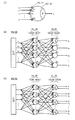
- the figure which shows the structural example of a neural network The figure which shows the operation example of a neural network.
- flowchart. flowchart.
- FIG. 7 shows a structural example of a transistor.
- FIG. 7 is a diagram showing an example of the configuration of a display panel.
- X and Y are connected, the case where X and Y are electrically connected, and X and Y function. It is assumed that the case where they are connected as well as the case where X and Y are directly connected are disclosed in this specification and the like. Therefore, the present invention is not limited to a predetermined connection relationship, for example, a connection relationship shown in a figure or a sentence, and anything other than the connection relationship shown in a figure or a sentence is also described in the figure or the sentence.
- X and Y each denote an object (eg, a device, an element, a circuit, a wiring, an electrode, a terminal, a conductive film, a layer, or the like).
- an element for example, a switch, a transistor, a capacitor, an inductor, a resistor, a diode, a display, or the like
- An element e.g., a switch, a transistor, a capacitive element, an inductor
- a resistance element e.g., a diode, a display element, a light emitting element, a load, and the like.
- an element for example, a switch, a transistor, a capacitor, an inductor, a resistor, a diode, a display, or the like
- the switch has a function of controlling on and off. That is, the switch is turned on or off and has a function of controlling whether current flows or not. Alternatively, the switch has a function of selecting and switching a path through which current flows.
- X and Y are electrically connected, the case where X and Y are directly connected shall be included.
- a circuit for example, a logic circuit (for example, an inverter, a NAND circuit, a NOR circuit, etc.) that enables functional connection of X and Y, signal conversion Circuits (DA converter circuit, AD converter circuit, gamma correction circuit, etc.), potential level converter circuits (power supply circuits (boost circuit, step-down circuit etc.), level shifter circuits for changing the potential level of signals, etc.) voltage source, current source, switching A circuit, an amplifier circuit (a circuit capable of increasing the signal amplitude or current amount, etc., an operational amplifier, a differential amplifier circuit, a source follower circuit, a buffer circuit, etc.), a signal generation circuit, a memory circuit, a control circuit, etc.
- a logic circuit for example, an inverter, a NAND circuit, a NOR circuit, etc.
- signal conversion Circuits DA converter circuit, AD converter circuit, gamma correction circuit, etc.
- potential level converter circuits power supply circuits (boost circuit, step-down
- X and Y are functionally connected if the signal output from X is transmitted to Y. Do. Note that when X and Y are functionally connected, the case where X and Y are directly connected and the case where X and Y are electrically connected are included.
- X and Y are electrically connected
- X and Y are electrically connected (ie, between X and Y).
- X and Y are functionally connected (that is, functionally connected with another circuit between X and Y).
- X and Y are directly connected (that is, when X and Y are connected without sandwiching another element or another circuit), the present specification.
- one component may have the functions of a plurality of components in combination. is there.
- one conductive film has both the function of the wiring and the function of the electrode. Therefore, the term "electrically connected" in this specification also falls under the category of one such conductive film, even when it has the function of a plurality of components.
- Embodiment 1 In the present embodiment, a virtual reality providing system according to an aspect of the present invention will be described.
- FIG. 1 shows a configuration example of a virtual reality providing system 10.
- the virtual reality providing system 10 includes a display unit 20, a measurement unit 30, and a control unit 40.
- the control unit 40 includes a neural network (NN) 50 and a signal generation unit 70. Further, the control unit 40 may have an arithmetic processing unit 80 or the like.
- NN neural network
- the measuring unit 30 measures the physiological condition of the user 60 when viewing an image (including an image) displayed on the display unit 20, and the neural network 50 measures the physiological data based on the measured data.
- Generate correction data The generated correction data is input to the processing circuit 73 of the signal generation unit 70.
- the processing circuit 73 data input to the display panel to display an image is corrected by the correction data and input to the display unit 20.
- the display unit 20 also has a display panel.
- each of the display unit 20 and the control unit 40 in the virtual reality providing system 10 can be configured by a semiconductor device.
- a liquid crystal element or a light emitting element can be used for the display panel included in the display unit 20.
- the circuits included in the control unit 40 can be integrated into one integrated circuit.
- the display unit 20 has a display panel. Each of the display panels has a function of displaying a video based on a signal (hereinafter also referred to as a video signal or an image signal) for displaying a predetermined video input from the signal generation unit 70.
- a signal hereinafter also referred to as a video signal or an image signal
- the display panel also includes a pixel portion formed of a plurality of pixels and a driver circuit (a gate line driver circuit or a source line driver circuit).
- a driver circuit a gate line driver circuit or a source line driver circuit.
- Each pixel has a display element and has a function of displaying a predetermined gray level. Then, the gray level of the pixel is controlled by the driver circuit and a signal output from the driver circuit, and a predetermined image is displayed on the pixel portion.
- a light emitting element or a liquid crystal element can be given.
- light emitting elements include self-luminous light emitting elements such as organic light emitting diodes (OLEDs), light emitting diodes (LEDs), quantum-dot light emitting diodes (QLEDs), and semiconductor lasers.
- the number of pixels provided in the pixel portion can be freely set. For example, in the case of displaying a 4K2K image on the display portion, it is preferable to provide a total of 3840 ⁇ 2160 pixels or more or 4096 ⁇ 2160 pixels or more in N ⁇ M display panels. In the case of displaying an 8K4K image, it is preferable to provide a total of 7680 ⁇ 4320 pixels or more. In addition, more pixels can be provided in the pixel portion.
- Each pixel is connected to the line (SL) and the line (GL).
- the lines (GL) are connected to the drive circuit (gate line drive circuit), and the lines (SL) are connected to the drive circuit (source line drive circuit).
- the driver circuit has a function of supplying a signal for selecting a pixel (hereinafter, also referred to as a selection signal) to the pixel.
- the driver circuit has a function of supplying a selection signal to the wiring (GL), and the wiring (GL) has a function of transmitting a selection signal output from the driver circuit to a pixel.
- the wiring (GL) can also be called a selection signal line, a gate line, or the like.
- the driver circuit has a function of supplying a video signal to a pixel. Specifically, the driver circuit has a function of supplying a video signal to the wiring (SL), and the wiring (SL) has a function of transmitting a video signal output from the driver circuit to a pixel.
- the wirings (SL) can also be called signal lines, source lines, and the like.
- the measuring unit 30 shown in FIG. 1 measures the physiological condition of the user 60 when viewing the image (including the image) displayed on the display unit 20, and the measured data is used as a neural network of the control unit 40. It has a function to input to the network 50.
- the measuring unit 30 has a measuring device capable of converting information (blood pressure, heart rate, amount of sweating, brain waves, etc.) indicating the physiological condition of the user 60 into data.
- a sphygmomanometer, a heart rate meter, a perspiration meter, an electroencephalograph etc. can be used as a measuring instrument.
- the measurement unit may be configured to measure the movement (the movement in response to the image, etc.) of the user 60 when viewing the image as the information included in the information of the physiological condition of the user 60.
- the image of the movement of the user 60 was measured using an image sensor (for example, a CCD image sensor, a CMOS image sensor, etc.), a camera, and other sensors, and data of position information and movement speed information etc. What is necessary is just to use.
- the measuring unit 30 can measure the physiological condition of the user 60 when viewing the image (including the image) displayed on the display unit 20.
- the control unit 40 illustrated in FIG. 1 includes a neural network (NN) 50 and a signal generation unit 70.
- the neural network 50 is data for correcting a video signal to perform display for reducing VR sickness based on the physiological state of the user 60 when viewing the video (including the image) displayed on the display unit 20.
- the signal generation unit 70 has a function of correcting a video signal input to the display unit.
- the configuration of the control unit 40 is not limited to the above, and a necessary circuit may be provided as needed.
- a neural network (NN) 50 included in the control unit 40 has a function of outputting correction data (NSD) for correcting video data (SD) input to the display unit 20.
- the neural network 50 is input to the display unit 20 and measurement data (DD) measured by the measurement unit 30 with respect to the physiological state of the user 60 when viewing the image (including the image) displayed on the display unit 20. From the video data (SD), learning is performed to output correction data (NSD) that enables video display to reduce VR sickness of the user 60 to the processing circuit 73.
- SD video data
- NSD correction data
- the neural network 50 infers and outputs correction data (NSD).
- the neural network 50 is configured of a neuron circuit (NC) 32 and a synapse circuit (SC) 31 provided between the neuron circuits.
- NC neuron circuit
- SC synapse circuit
- Input data x 1 to x L (L is a natural number) are input to the synapse circuit (SC) 31.
- the synapse circuit 31 has a function of storing a weight coefficient w k (k is an integer of 1 or more and L or less). Weight coefficient w k corresponds to the strength of binding between the neuron circuit (NC) 32.
- the neuron circuit 32 When the input data x 1 to x L is input to the synapse circuit 31, the product of the input data x k input to the synapse circuit 31 and the weight coefficient w k stored in the synapse circuit 31 is input to the neuron circuit 32.
- a value (x 1 w 1 + x 2 w 2 +... + X L w L ) obtained by adding (x k w k ) for k 1 to L, that is, obtained by a product-sum operation using x k and w k
- the supplied value is supplied.
- this value exceeds the threshold ⁇ of the neuron circuit 32, the neuron circuit 32 outputs a high level signal. This phenomenon is called firing of the neuron circuit 32.
- FIG. 2B shows a model of a neural network 50 that constitutes a hierarchical perceptron by using a neuron circuit 32 and a synapse circuit 31.
- the neural network 50 has an input layer (IL) 33, a hidden layer (intermediate layer: HL) 34, and an output layer (OL) 35.
- IL input layer
- HL hidden layer
- OL output layer
- Input data x 1 to x L are output from the input layer 33.
- the hidden layer 34 has a hidden synapse circuit (HS) 36 and a hidden neuron circuit (HN) 37.
- the output layer 35 has an output synapse circuit (OS) 38 and an output neuron circuit (ON) 39.
- the hidden neuron circuit 37, the input data x k, the value obtained by the product-sum operation using a weight coefficient w k held in the hidden synapse circuit 36 is supplied.
- the output neuron circuit 39, the output of the hidden neuron circuit 37, the value obtained by the product-sum operation using a weight coefficient w k held in the output synapse circuit 38 is supplied.
- output data y 1 to y L are output from the output neuron circuit 39.
- the neural network 50 in which a predetermined input data is given, a weight factor w k held in the synapse circuit 31, a value corresponding to the threshold value ⁇ of the neuron circuit 32, the function of outputting as output data .
- the neural network 50 can perform supervised learning by inputting teacher data.
- FIG. 2C shows a model of a neural network 50 that performs supervised learning using an error back propagation method.
- the error ⁇ O of the neural network 50 described above is obtained by measuring the measurement data (DD) measured by the measuring instrument 30 and the video data before correction (by decoding the broadcast signal. It can be determined based on the acquired video data) (SD) (teacher data).
- the hidden layer 34 of one layer is shown in FIG. 2 (B) and (C), the number of layers of the hidden layer 34 can be two or more. Deep learning can be performed by using a neural network (deep neural network (DNN)) having two or more hidden layers 34. Thereby, the accuracy of gradation correction can be enhanced.
- DNN deep neural network
- a function of correcting video data (SD) is added by learning. Then, when the video data (SD) is input to the neural network 50, arithmetic processing is performed in each layer. Arithmetic processing in each layer is performed by a product-sum operation of the output of the neuron circuit of the front layer and the weighting factor.
- the layer-to-layer connection may be a full connection in which all neuron circuits are connected to each other, or a partial connection in which some neuron circuits are connected to each other.
- the calculation result is output from the output layer OL as correction data (NSD). Thereby, the video data (SD) is corrected to the video data (SD ').
- FIG. 3 shows how the neural network 50 outputs correction data of video data (SD). Note that parallel processing using a plurality of neural networks 50 can also be performed, and in this case, correction of video data (SD) can be performed at high speed.
- the correction data (NSD) is output from the output layer (OL) 35 of the neural network 50 and is output to the processing circuit 73. As described above, by using the correction data (NSD) corrected by the neural network 50, it is possible to display an image in which the VR sickness of the user 60 is reduced.
- the number of neural networks 50 is not particularly limited, and can be set freely.
- video data (SD) is input to the neural network 50 and inference is performed.
- a weighting factor is input to the neural network 50 as correction processing of the video data (SD)
- a weighting factor (w) is used for correction of the video data (SD).
- a plurality of neural networks may be provided, and a plurality of data may be sequentially input to each neural network.
- data since data is sequentially input, it is preferable to switch the weighting factors at high speed.
- the structure suitable for switching of a weighting factor it can use combining a well-known method suitably.
- the measurement data (DD) measured by the measurement unit 30 with respect to the physiological state of the user 60 when viewing the image (including the image) displayed on the display unit 20 and the image data input to the display unit 20 (SD) is input to the neural network 50, and correction data (NSD) in which a weighting factor for reducing VR sickness of the user 60 is set is output from the neural network 50 to the processing circuit 73.
- NSD correction data
- video data (SD) is input to the neural network 50 (step S1).
- the neural network 50 is in a state before learning, and correction data (NSD) corresponding to the initial value of the weighting factor is output from the neural network 50 to the processing circuit 73.
- the video data (SD) is assumed to be a video signal corresponding to the video A.
- the video data (SD ') corrected by the correction data (NSD) is supplied from the processing circuit 73 to the display unit 20, and the video B is displayed on the display unit 20 (step S2).
- VR sickness may occur to the user 60 who has viewed the video (including the image) displayed on the display unit 20.
- the degree of VR sickness can be evaluated based on measurement data (DD) measured for parameters (blood pressure, heart rate, amount of sweating, brain waves, etc.) indicating the physiological condition of the user 60. Therefore, the degree of VR sickness is included in the measurement data (DD) measured by the measurement unit 30 (step S3).
- video data (SD) is input to the neural network 50 (step S4).
- Image data (SD) is supplied to the input layer 33 of the neural network 50, and displayed on the display unit 20 so that the value of the measurement data (DD) becomes a desired value (value in a range that does not cause VR sickness).
- Weight coefficients of the neural network 50 are updated (step S5). An error back propagation method or the like can be used to update the weighting factor.
- the correction data (NSD) output from the neural network 50 is also updated with the update of the weighting factor. Also, the measurement data (DD) is updated by updating the correction data (NSD). Then, the weighting factor is further updated based on the updated measurement data (DD).
- the above-described updating of the weighting factor is repeated until the value of the measurement data (DD) reaches a desired range of values (a range of values which does not cause VR sickness which has been measured in advance). Also, the tolerance of the error can be freely set. Then, when the measurement data (DD) finally becomes a value in a desired range (a value in a range not causing VR sickness which is measured in advance), learning of the neural network 50 is ended (YES in step S6). Then, the weighting factor W of the neural network 50 at this time is obtained as a learning result.
- the initial value of the weighting factor of the neural network 50 may be determined by a random number.
- the initial value of the weighting factor may affect the learning speed (for example, the convergence speed of the weighting factor, the prediction accuracy of the neural network 50, etc.). Therefore, when the learning speed is slow, change the initial value of the weighting factor. You may
- step S7 Thereafter, when learning is continued using another video (NO in step S7), the operations in and after step S1 are repeated. Then, when learning is completed for all the videos (YES in step S7), learning of the neural network 50 ends.
- the learning of the neural network 50 described above can be performed using an arithmetic processing unit 80 (FIG. 1) or the like provided inside (or outside) of the control unit 40.
- arithmetic processing unit 80 a computer with excellent arithmetic processing capability such as a dedicated server or a cloud can be used.
- software corresponding to the neural network 50 in the arithmetic processing unit 80, learning of the neural network 50 can be performed on software using the arithmetic processing unit 80. Then, by supplying the weighting coefficient W obtained by learning using software to the neural network 50, the learning result can be reflected on the neural network 50.
- a hierarchical perceptron is used, and a method of constructing on the software a neural network having the same number of layers as the neural network 50 and the number of neurons included in each layer. Can be used.
- the learning of the neural network 50 may be performed by parallel processing in which video data (SD) is input to a plurality of neural networks 50, or video data (SD) is sequentially input to one neural network 50. You may go.
- SD video data
- SD video data
- video data (SD) generated by the processing circuit 73 of the signal generation unit 70 is input to the neural network 50 (step S11). Then, the neural network 50 infers using the video data (SD) as input data, and generates correction data (NSD) for correcting the video data (SD) (step S12).
- SD video data
- NSD correction data
- the neural network 50 is trained so as to reduce the VR sickness of the user when viewing the image B. Therefore, when the correction data (NSD) obtained by the inference of the neural network 50 is input to the processing circuit 73 and the data (SD ') corrected from the processing circuit 73 is output to the display unit 20 (step S13) , An image with reduced VR sickness of the user is displayed (step S14).
- the image data (SD) is corrected using the neural network 50 to reduce VR sickness according to the user's physiological condition. It is characterized by performing display.
- the signal generation unit 70 included in the control unit 40 has a function of generating a video signal based on data input from the outside.
- the signal generation unit 70 includes a front end unit (FE) 71, a decoder (DEC) 72, a processing circuit (PC) 73, a reception unit (RCV) 74, an interface (IF) 75, and a control circuit (CTRL) 76.
- FE front end unit
- DEC decoder
- PC processing circuit
- RCV reception unit
- IF interface
- CTRL control circuit
- the front end unit 71 has a function of receiving a signal input from the outside and appropriately performing signal processing.
- the front end unit 71 receives, for example, a broadcast signal that has been encoded and modulated according to a predetermined method.
- the front end unit 71 can have a function of demodulating a received video signal, performing analog-digital conversion, and the like.
- the front end unit 71 may have a function of performing error correction.
- the data received by the front end unit 71 and subjected to the signal processing is output to the decoder 72.
- the decoder 72 has a function of decoding the encoded signal. When the video data included in the broadcast signal input to the front end unit 71 is compressed, the decoder 72 performs decompression.
- the decoder 72 can have a function of performing inverse orthogonal transformation such as entropy decoding, inverse quantization, inverse discrete cosine transformation (IDCT), inverse discrete sine transformation (IDST), intra-frame prediction, inter-frame prediction, etc. .
- the coding standard for 8K / 4K television broadcasting includes H.323 and H.323.
- H.265 / MPEG-H High Efficiency Video Coding (hereinafter referred to as HEVC) is employed.
- the decoder 72 performs decoding (decoding) according to the HEVC.
- Video data (SD) generated by the decoding process by the decoder 72 is output to the neural network 50 and the processing circuit 73, respectively.
- the processing circuit 73 has a function of converting the video data (SD) input from the decoder 72 into a frame frequency based on the correction data (NSD) input from the neural network 50. That is, when the user 60 sees an image (including an image) displayed on the display unit 20, the image data (SD) is corrected to reduce the VR sickness of the user 60, and the display unit 20 is corrected. It has a function of inputting the corrected video data (SD ').
- the neural network 50 determines from the biological information, and correction data (NSD) based on it is sent, Perform processing to lower the video speed (drop the frame frequency) to the video data (SD), and that VR sickness is caused due to the video speed being slower than the user's sense .
- NSD biological information and correction data
- processing processing to increase the frame frequency for increasing the video speed with respect to the video data (SD) is performed. It can be carried out.
- the frame frequency is lowered to reduce power consumption in the case of normal display, and the image is displayed, and the frame frequency is changed when the display content changes significantly, such as when the user moves fast. It is also possible to reduce the VR sickness by raising the video so as to follow the action of the user.
- the video data (SD) input from the decoder 72 can be processed at the maximum by the signal generation unit 70 so that the processing circuit 73 can change the video speed to either high speed or low speed. It is preferable to keep the frequency of
- the processing circuit 73 may have a function of executing inter-frame interpolation processing and the like accompanying up-conversion of the frame frequency of the video speed. Further, it may have a function of performing inter-pixel interpolation processing accompanying resolution up-conversion. In addition, the processing circuit 73 may have a function of performing data division and video processing. Examples of video processing include noise removal processing, tone conversion processing, color tone correction processing, and luminance correction processing. Color tone correction processing and luminance correction processing can be performed using gamma correction or the like.
- the inter-frame interpolation process generates an image of a frame (interpolated frame) which does not originally exist when increasing the frame frequency of the image to be displayed.
- an image of an interpolation frame to be inserted between two images is generated from the difference between two images.
- images of a plurality of interpolation frames can be generated between two images.
- the frame frequency of the image data is 60 Hz
- the frame frequency of the image signal output to the display unit 20 can be doubled by 120 Hz, or quadrupled by 240 Hz, by generating a plurality of interpolation frames. It can be increased to eight times 480 Hz and so on.
- the inter-pixel interpolation process is a process of interpolating data which is not originally present when the resolution is upconverted. For example, reference is made to pixels around the target pixel, and the data is interpolated to display their intermediate colors.
- the noise removal process includes removal of various noises such as mosquito noise generated around the outline of characters, block noise generated by high-speed moving images, random noise causing flicker, dot noise generated by resolution up-conversion, etc. .
- the gradation conversion processing is processing for converting the gradation indicated by the data (SDdiv) into a gradation corresponding to the output characteristic of the display unit 20. For example, in the case where the number of gradations is increased, processing for smoothing the histogram can be performed by interpolating and allocating gradation values corresponding to each pixel to an image input with a small number of gradations. Also, high dynamic range (HDR) processing, which extends the dynamic range, is also included in the tone conversion processing.
- HDR high dynamic range
- the color tone correction processing is processing for correcting the color tone of an image.
- the luminance correction processing is processing for correcting the brightness (luminance contrast) of an image. For example, the luminance and the color tone of the image displayed on the display unit 20 are corrected so as to be optimal according to the type and the luminance or the color purity of the illumination in the space where the display unit 20 is provided.
- the receiving unit 74 has a function of receiving externally input data or control signals.
- a remote controller, a portable information terminal (such as a smartphone or a tablet), an operation button provided on the display unit 20, or the like can be used to input data or a control signal to the reception unit 74.
- the interface 75 has a function of appropriately performing signal processing on the data or control signal received by the receiving unit 74 and outputting the data or control signal to the control circuit 76.
- the control circuit 76 has a function of supplying a control signal to each circuit included in the signal generation unit 70.
- the control circuit 76 has a function of supplying a control signal to the decoder 72 or the processing circuit 73.
- the control by the control circuit 76 can be performed based on the control signal or the like received by the receiving unit 74.
- a video signal corrected using artificial intelligence in accordance with the physiological condition of the user 60 when viewing the video (including the image) displayed on the display unit 20 is By supplying the display unit 20, VR sickness of the user 60 can be reduced.
- a pixel unit and a driver circuit of a display panel included in the display unit 20 (see FIG. 1), and a control unit 40 (for example, a neural network (for example, a neural network NN) 50), and a specific configuration example of a transistor applicable to a signal generation unit 70 (for example, a processing circuit or a control circuit) will be described with reference to FIG.
- a control unit 40 for example, a neural network (for example, a neural network NN) 50
- a specific configuration example of a transistor applicable to a signal generation unit 70 for example, a processing circuit or a control circuit
- the transistors shown in FIGS. 6A to 6E are OS transistors in which a metal oxide is used for the semiconductor layer 432.
- the frequency of updating the image signal can be set extremely low in a period in which there is no change in the image or in a period in which the change is less than or equal to a certain amount, and power consumption can be reduced.
- the insulating layer 484 is provided over the channel formation region of the semiconductor layer 432.
- the insulating layer 484 functions as an etching stopper when the semiconductor layer 432 is etched.
- the transistor illustrated in FIG. 6B has a structure in which the insulating layer 484 extends over the semiconductor layer 432 and over the insulating layer 434.
- the conductive layer 433a and the conductive layer 433b are connected to the semiconductor layer 432 through an opening provided in the insulating layer 484.
- the transistor illustrated in FIG. 6C includes an insulating layer 485 and a conductive layer 486.
- the insulating layer 485 is provided to cover the semiconductor layer 432, the conductive layer 433a, and the conductive layer 433b.
- the conductive layer 486 is provided over the insulating layer 485 and has a region overlapping with the semiconductor layer 432.
- the conductive layer 486 is opposite to the conductive layer 431 with the semiconductor layer 432 interposed therebetween.
- the conductive layer 431 is a first gate electrode
- the conductive layer 486 can function as a second gate electrode.
- the threshold voltage of the transistor can be controlled by applying a potential for controlling the threshold voltage to one of the conductive layers 431 and 486 and a potential for driving the other.
- the transistor illustrated in FIG. 6D is a top-gate transistor, and the conductive layer 431 functioning as a gate electrode is provided above the semiconductor layer 432 (the side opposite to the formation surface side).
- the insulating layer 434 and the conductive layer 431 are stacked over the semiconductor layer 432.
- the insulating layer 482 is provided to cover the top surface and the side end portion of the semiconductor layer 432, and the conductive layer 431.
- the conductive layer 433a and the conductive layer 433b are provided over the insulating layer 482.
- the conductive layer 433a and the conductive layer 433b are connected to the semiconductor layer 432 through an opening provided in the insulating layer 482.
- the insulating layer 434 may be provided to cover the top surface and the side end portion of the semiconductor layer 432.
- the transistor illustrated in FIG. 6D can easily reduce the parasitic capacitance between the conductive layer 431 and the conductive layer 433a or the conductive layer 433b because they are easily separated.
- the transistor illustrated in FIG. 6E is different from that in FIG. 6D in that the conductive layer 487 and the insulating layer 488 are included.
- the conductive layer 487 has a region overlapping with the semiconductor layer 432.
- the insulating layer 488 is provided to cover the conductive layer 487.
- the conductive layer 487 functions as a second gate electrode. Therefore, it is possible to increase the on current, control the threshold voltage, and the like.
- the semiconductor layer 432 may have a region 432n.
- the region 432 n includes a region in contact with the insulating layer 482 containing nitrogen or hydrogen. Then, nitrogen or hydrogen in the insulating layer 482 is added to the region 432 n, whereby the region 432 n is n-typed. In this case, the region 432 n functions as a source region or a drain region. Note that the concentration of nitrogen or hydrogen contained in the region 432 n is higher than that of the channel formation region. In addition, the carrier density of the region 432 n is higher than that of the channel formation region.
- the semiconductor layer 432 may have a region 432 j.
- the region 432 j functions as a junction region between the channel formation region and the source or drain region.
- the concentration of nitrogen or hydrogen contained in the region 432 j is lower than the region 432 n and higher than the channel formation region.
- the carrier density of the region 432 j is lower than that of the region 432 n and higher than that of the channel formation region.
- a transistor in which a semiconductor containing silicon is used for the semiconductor layer 432 may be used.
- a semiconductor containing silicon for example, hydrogenated amorphous silicon, microcrystalline silicon, polycrystalline silicon, or the like can be used.
- Low power consumption can be achieved by applying to (for example, neural network (NN) 50), signal generation unit 70 (for example, processing circuit or control circuit), and the like.
- NN neural network
- signal generation unit 70 for example, processing circuit or control circuit
- FIG. 7A is a top view of the display panel 21, and FIG. 7B is a cross-sectional view of FIG. 7A taken along a dashed-dotted line AA '.
- An active matrix display panel includes a pixel portion 302, a driver circuit portion (source line driver circuit) 303, and driver circuit portions (gate line driver circuits) (304a and 304b) provided over a first substrate 301. .
- the pixel portion 302 and the driver circuit portions 303, 304 a, 304 b are sealed between the first substrate 301 and the second substrate 306 by the sealant 305.
- a lead wiring 307 is provided over the first substrate 301.
- the lead wiring 307 is connected to the FPC 308 which is an external input terminal.
- the FPC 308 transmits signals (eg, video signals, clock signals, start signals, reset signals, and the like) and potentials from the outside to the driver circuit units (303, 304a, and 304b).
- a printed wiring board (PWB) may be attached to the FPC 308. Note that the state in which the FPC and the PWB are attached is included in the display panel.
- the image speed is changed according to the physiological condition of the user by the correction signal output from the neural network in order to reduce VR sickness. Therefore, the video signal input to the display panel described in this embodiment is changed in accordance with the physiological condition of the user. Therefore, it is preferable to provide a variable circuit or the like that can change the drive frequency of the drive circuit that constitutes the display panel.
- the pixel portion 302 includes a plurality of FETs (switching FETs) 311, FETs (current control FETs) 312, and a plurality of first electrodes 313 electrically connected to the FETs 312.
- FETs switching FETs
- FETs current control FETs
- first electrodes 313 electrically connected to the FETs 312.
- the FETs 309, 310, 311, and 312 are not particularly limited, and, for example, transistors such as a staggered transistor or an inverted staggered transistor can be applied. In addition, a top gate type or bottom gate type transistor structure may be employed.
- the crystallinity of the semiconductor that can be used for these FETs 309, 310, 311, and 312 is not particularly limited, and an amorphous semiconductor, a semiconductor having crystallinity (a microcrystalline semiconductor, a polycrystalline semiconductor, a single crystal semiconductor, Alternatively, any of semiconductors each having a crystal region in part may be used. Note that using a semiconductor having crystallinity is preferable because deterioration of transistor characteristics can be suppressed.
- an element of Group 14 a compound semiconductor, an oxide semiconductor, an organic semiconductor, or the like can be used.
- a semiconductor containing silicon, a semiconductor containing gallium arsenide, an oxide semiconductor containing indium, or the like can be used.
- the driver circuit portion 303 includes an FET 309 and an FET 310.
- the FET 309 and the FET 310 may be formed by a circuit including a unipolar (N-type or P-type) transistor, or may be formed by a CMOS circuit including an N-type transistor and a P-type transistor. It is good.
- a driver circuit may be provided outside.
- the end of the first electrode 313 is covered with an insulator 314.
- an organic compound such as a negative photosensitive resin or a positive photosensitive resin (acrylic resin), or an inorganic compound such as silicon oxide, silicon oxynitride, or silicon nitride can be used.
- the insulator 314 preferably has a curved surface having a curvature at the upper end or the lower end. Thus, the coverage of the film formed on the upper layer of the insulating portion 314 can be made favorable.
- the EL layer 315 and the second electrode 316 are stacked over the first electrode 313, and the light emitting element 317 is formed of the first electrode 313, the EL layer 315, and the second electrode 316.
- the EL layer 315 includes a light emitting layer, a hole injecting layer, a hole transporting layer, an electron transporting layer, an electron injecting layer, a charge generation layer, and the like.
- a known structure or a known material can be applied.
- the second electrode 316 is electrically connected to the FPC 308 which is an external input terminal.
- a plurality of light emitting elements are arranged in a matrix.
- Light-emitting elements which can emit light of three types (R, G, and B) can be selectively formed in the pixel portion 302, so that a light-emitting device capable of full-color display can be formed.
- light emitting elements that can obtain three types (R, G, B) of light emissions, light emissions such as white (W), yellow (Y), magenta (M), cyan (C), etc.
- An element may be formed.
- a light emitting element capable of obtaining the above-described several types of light emission to a light emitting element capable of obtaining three types of light emission (R, G, B)
- effects such as improvement of color purity and reduction of power consumption can be obtained.
- a light emitting device capable of full color display may be provided by combining with a color filter.
- red (R), green (G), blue (B), cyan (C), magenta (M), yellow (Y) etc. can be used as a kind of color filter.
- the FETs (309, 310, 311, and 312) and the light emitting element 317 on the first substrate 301 are attached to each other with the sealant 305 so that the second substrate 306 and the first substrate 301 are bonded to each other.
- a structure provided in a space 318 surrounded by the second substrate 301 and the sealing material 305 is provided.
- the space 318 may be filled with an inert gas (such as nitrogen or argon) or an organic substance (including the sealant 305).
- sealing material 305 an epoxy resin or glass frit can be used. Note that for the sealing material 305, it is preferable to use a material that does not transmit moisture or oxygen as much as possible.
- first substrate 301 and the second substrate 306 in addition to a glass substrate and a quartz substrate, plastic substrates made of FRP (Fiber-Reinforced Plastics), PVF (polyvinyl fluoride), polyester, acrylic, or the like can be used. .
- FRP Fiber-Reinforced Plastics
- PVF polyvinyl fluoride
- polyester acrylic
- acrylic acrylic
- the FET and the light emitting element may be formed directly on the flexible substrate, but the FET and the light emitting element are formed on another substrate having a peeling layer. After formation, the FET and the light emitting element may be separated by a peeling layer by applying heat, force, laser irradiation, or the like, and may be further transferred to a flexible substrate.
- the peeling layer for example, a lamination of an inorganic film of a tungsten film and a silicon oxide film, an organic resin film such as polyimide, or the like can be used.
- a flexible substrate In addition to the flexible substrate among the above-described substrate materials capable of forming a transistor as a flexible substrate, a paper substrate, a cellophane substrate, an aramid film substrate, a polyimide film substrate, a cloth substrate (natural fiber (Silk, cotton, hemp), synthetic fiber (nylon, polyurethane, polyester) or regenerated fiber (including acetate, cupra, rayon, regenerated polyester) and the like, a leather substrate, a rubber substrate and the like.
- a cloth substrate natural fiber (Silk, cotton, hemp), synthetic fiber (nylon, polyurethane, polyester) or regenerated fiber (including acetate, cupra, rayon, regenerated polyester) and the like
- a leather substrate a rubber substrate and the like.
- an active matrix display panel in which a light emitting element is used as a display element and a transistor (FET) is combined is described as a display panel applicable to the display portion of the virtual reality providing system.
- FET transistor
- the present invention is not limited to this, and a liquid crystal element can also be used as a display element.
- Embodiment 4 a head mounted display (HMD) which can be applied to a display portion of a virtual reality providing system which is an embodiment of the present invention will be described with reference to FIG.
- HMD head mounted display
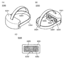
- FIGS. 8A, 8B, and 8C show the appearance of the HMD 8300.
- the HMD 8300 includes a housing 8301, a display portion 8302, a band-like fixing tool 8304, and a pair of lenses 8305.
- the user can view the display on the display portion 8302 through the lens 8305.
- the display portion 8302 is preferably curved and disposed. By arranging the display portion 8302 in a curved manner, the user can feel a high sense of reality.
- the present invention is not limited to this. For example, two display portions 8302 may be provided. In this case, if one display unit is disposed in one eye of the user, three-dimensional display or the like using parallax can be performed.
- 10 virtual reality providing system 20: display unit 30: measurement unit 31: synapse circuit (SC) 32: neuron circuit (NC) 33: input layer (IL) 34: hidden layer (intermediate layer: HL) ), 35: output layer (OL), 36: hidden synapse circuit (HS), 37: hidden neuron circuit (HN), 38: output synapse circuit (OS), 39: output neuron circuit (ON), 50: neural network , 60: user, 70: signal generator, 71: front end (FE), 72: decoder (DEC), 73: processing circuit (PC), 74: receiver (RCV), 75: interface (IF) , 76: control circuit (CTRL), 80: arithmetic processing unit, 301: first substrate, 302: pixel portion, 303: drive circuit portion (source line drive circuit), 304a, 304b: drive Circuit portion (gate line drive circuit) 305: seal material 306: second substrate 307: lead wiring 308: FPC 309: FET 310: FET 311:
Landscapes
- Engineering & Computer Science (AREA)
- Theoretical Computer Science (AREA)
- General Engineering & Computer Science (AREA)
- Physics & Mathematics (AREA)
- General Physics & Mathematics (AREA)
- Multimedia (AREA)
- Signal Processing (AREA)
- Human Computer Interaction (AREA)
- Computer Hardware Design (AREA)
- Controls And Circuits For Display Device (AREA)
Abstract
要約書 新規な仮想現実提供システムを提供する。 仮想現実提供システムは、 人工知能 (AI:Artificial Intelligence) を 利用して映像(画像を含む)信号を補正する機能を有する。具体的には、表示された映像(画像を含 む) を見た際の使用者の生理状態を計測部が測定し、 測定されたデータを基にニューラルネットワー クにより補正データを生成する。得られた補正データに基づき映像信号を補正して表示することによ り、映像を見た使用者のVR酔いを低減することができる。
Description
本発明の一態様は、VR酔いを低減することができる仮想現実提供システムに関する。
なお、本発明の一態様は、上記の技術分野に限定されない。本明細書等で開示する本発明の一態様の技術分野としては、半導体装置、表示装置、発光装置、蓄電装置、記憶装置、表示システム、電子機器、照明装置、入力装置、入出力装置、それらの駆動方法、又はそれらの製造方法、を一例として挙げることができる。
また、本明細書等において、半導体装置とは、半導体特性を利用することで機能しうる装置全般を指す。トランジスタ、半導体回路、演算装置、記憶装置等は半導体装置の一態様である。また、撮像装置、電気光学装置、発電装置(薄膜太陽電池、有機薄膜太陽電池等を含む)、及び電子機器は半導体装置を有している場合がある。
コンピュータグラフィックスを用いて三次元の仮想世界を立体視できる技術がある。また、この技術を用いて表示された画像の視聴には、頭部または顔部に装着して利用されるヘッドマウントディスプレイ(HMD)が知られている。このHMDは、使用者の視線方向に合わせて表示映像を切り替えることが可能であるので、臨場感のある画像を体験することができる。
しかし、このようなHMDでは、視界の大部分を表示された画像が占めることになるため、「ヴァーチャル・リアリティー(VR)酔い」と呼ばれる酔いの症状が出ることが知られている。なお、VR酔いの原因は、提供される画像と使用者が体感する画像との間の視野角の不一致や、奥行き感の不一致であるといわれている。
これに対して、画像表示において、二次元情報と三次元仮想物体の両方を合成情報として用いることで、VR酔いを低減しつつ臨場感を維持するという技術が開発されている(例えば、特許文献1)。
本発明の一態様では、単に映像の表示方法を変えるのではなく、使用者の生理状態に応じた映像表示を実現することにより、VR酔いを低減することを目的とする。従って、本発明の一態様は、新規な仮想現実提供システムを提供する。また、本発明の一態様は、使用者の生理状態に応じた映像表示を行い、VR酔いを低減することができる仮想現実提供システムを提供する。
なお、本発明の一態様は、必ずしも上記の課題の全てを解決する必要はなく、少なくとも一の課題を解決できるものであればよい。また、上記の課題の記載は、他の課題の存在を妨げるものではない。これら以外の課題は、明細書、特許請求の範囲、図面などの記載から、自ずと明らかとなるものであり、明細書、特許請求の範囲、図面などの記載から、これら以外の課題を抽出することが可能である。
本発明の一態様に係る仮想現実提供システムは、人工知能(AI:Artificial Intelligence)を利用して映像(画像を含む)信号を補正する機能を有する。具体的には、表示された映像(画像を含む)を見た際の使用者の生理状態を計測部が測定し、測定されたデータを基に人工ニューラルネットワーク(ANN:Artificial Neural Network)により補正データを生成する。さらに補正データに基づき映像信号を補正して表示することにより、映像を見た使用者のVR酔いを低減することができる。
なお、人工知能とは、人間の知能を模した計算機である。また、人工ニューラルネットワークとは、ニューロンとシナプスで構成される神経網を模した回路であり、人工知能の一種である。本明細書等において「ニューラルネットワーク」と記載する場合、特に人工ニューラルネットワークを指す。
本発明の一態様は、表示部と、制御部とを有し、表示部は、映像を表示することによって仮想現実を使用者に提供し、制御部は、ニューラルネットワークを有し、ニューラルネットワークは学習内容に基づき、使用者の生理状態に応じて酔いを低減する補正データを出力し、制御部は、補正データに基づき、映像を補正して表示部に表示させる仮想現実提供システムである。
本発明の別の一態様は、表示部と、制御部と、計測部と、を有し、表示部は、第1のデータに基づく映像を表示することによって仮想現実を使用者に提供し、制御部は、ニューラルネットワークを有し、計測部は、映像を見た際の使用者の生理状態に基づく第2のデータを測定し、ニューラルネットワークは、第1のデータと第2のデータに基づき、使用者の生理状態に応じて、酔いを低減する第3のデータを出力し、制御部は、第3のデータに基づき、映像を補正して表示部に表示させる仮想現実提供システムである。
なお、上記構成において、ニューラルネットワークは、第1のデータと第2のデータに基づき、ニューラルネットワークの重みを更新して、酔いを低減する第3のデータを出力し、第3のデータに基づき、映像を補正することにより学習を行うことを特徴とする。
なお、上記各構成において、計測部は、使用者の生理状態の情報として、血圧、心拍数、発汗量または脳波のいずれかを測定することを特徴とする。また、計測部が、使用者の生理状態の情報に含まれる情報として、映像を見た際の使用者の動き(映像に反応した動き等)を測定する構成とすることもできる。この場合は、使用者の動きの映像をイメージセンサ(例えば、CCDイメージセンサ、CMOSイメージセンサ等)、カメラ、その他センサを用いて測定し、位置情報や動きの速さ情報などをデータ化したものを用いればよい。
また、上記各構成において、使用者は、血圧、心拍数、発汗量または脳波の測定により、生理状態がモニタされることを特徴とする。また、上記各構成において、使用者は、位置情報や動きの速さ情報等を測定することにより、映像を見た際の使用者の動き(映像に反応した動き等)がモニタされることを特徴とする。
また、本発明の一態様に係る仮想現実提供システムにおいて、表示部には、様々な素子を用いることができる。なお、素子としては、公知の様々な素子を適用することができるが、液晶素子や発光素子等を用いることが好ましい。
また、本発明の一態様に係る仮想現実提供システムにおいて、ニューラルネットワークにデータを順次入力し、データごとに異なる重み係数を用いてデータの補正を行ってもよい。
本発明の一態様により、新規な仮想現実提供システムを提供することができる。また、本発明の一態様により、使用者の生理状態に応じた映像表示を行い、VR酔いを低減することができる仮想現実提供システムを提供することができる。
なお、これらの効果の記載は、他の効果の存在を妨げるものではない。また、本発明の一態様は、必ずしも、これらの効果の全てを有する必要はない。これら以外の効果は、明細書、特許請求の範囲、図面などの記載から、自ずと明らかとなるものであり、明細書、特許請求の範囲、図面などの記載から、これら以外の効果を抽出することが可能である。
以下、本発明の実施の形態について図面を用いて詳細に説明する。ただし、本発明は以下の実施の形態における説明に限定されず、本発明の趣旨及びその範囲から逸脱することなくその形態及び詳細を様々に変更し得ることは、当業者であれば容易に理解される。したがって、本発明は、以下に示す実施の形態の記載内容に限定して解釈されるものではない。
また、本明細書等において、XとYとが接続されている、と明示的に記載されている場合は、XとYとが電気的に接続されている場合と、XとYとが機能的に接続されている場合と、XとYとが直接接続されている場合とが、本明細書等に開示されているものとする。したがって、所定の接続関係、例えば、図又は文章に示された接続関係に限定されず、図又は文章に示された接続関係以外のものも、図又は文章に記載されているものとする。ここで、X、Yは、対象物(例えば、装置、素子、回路、配線、電極、端子、導電膜、層、など)であるとする。
XとYとが直接的に接続されている場合の一例としては、XとYとの電気的な接続を可能とする素子(例えば、スイッチ、トランジスタ、容量素子、インダクタ、抵抗素子、ダイオード、表示素子、発光素子、負荷など)が、XとYとの間に接続されていない場合であり、XとYとの電気的な接続を可能とする素子(例えば、スイッチ、トランジスタ、容量素子、インダクタ、抵抗素子、ダイオード、表示素子、発光素子、負荷など)を介さずに、XとYとが、接続されている場合である。
XとYとが電気的に接続されている場合の一例としては、XとYとの電気的な接続を可能とする素子(例えば、スイッチ、トランジスタ、容量素子、インダクタ、抵抗素子、ダイオード、表示素子、発光素子、負荷など)が、XとYとの間に1個以上接続されることが可能である。なお、スイッチは、オンオフが制御される機能を有している。つまり、スイッチは、オン状態、又は、オフ状態になり、電流を流すか流さないかを制御する機能を有している。又は、スイッチは、電流を流す経路を選択して切り替える機能を有している。なお、XとYとが電気的に接続されている場合は、XとYとが直接的に接続されている場合を含むものとする。
XとYとが機能的に接続されている場合の一例としては、XとYとの機能的な接続を可能とする回路(例えば、論理回路(インバータ、NAND回路、NOR回路など)、信号変換回路(DA変換回路、AD変換回路、ガンマ補正回路など)、電位レベル変換回路(電源回路(昇圧回路、降圧回路など)、信号の電位レベルを変えるレベルシフタ回路など)、電圧源、電流源、切り替え回路、増幅回路(信号振幅又は電流量などを大きく出来る回路、オペアンプ、差動増幅回路、ソースフォロワ回路、バッファ回路など)、信号生成回路、記憶回路、制御回路など)が、XとYとの間に1個以上接続されることが可能である。なお、一例として、XとYとの間に別の回路を挟んでいても、Xから出力された信号がYへ伝達される場合は、XとYとは機能的に接続されているものとする。なお、XとYとが機能的に接続されている場合は、XとYとが直接的に接続されている場合と、XとYとが電気的に接続されている場合とを含むものとする。
なお、XとYとが電気的に接続されている、と明示的に記載されている場合は、XとYとが電気的に接続されている場合(つまり、XとYとの間に別の素子又は別の回路を挟んで接続されている場合)と、XとYとが機能的に接続されている場合(つまり、XとYとの間に別の回路を挟んで機能的に接続されている場合)と、XとYとが直接接続されている場合(つまり、XとYとの間に別の素子又は別の回路を挟まずに接続されている場合)とが、本明細書等に開示されているものとする。つまり、電気的に接続されている、と明示的に記載されている場合は、単に、接続されている、とのみ明示的に記載されている場合と同様な内容が、本明細書等に開示されているものとする。
また、図面上は独立している構成要素同士が電気的に接続しているように図示されている場合であっても、1つの構成要素が、複数の構成要素の機能を併せ持っている場合もある。例えば配線の一部が電極としても機能する場合は、一の導電膜が、配線の機能と電極の機能を両方併せ持っている。したがって、本明細書における電気的に接続とは、このような、一の導電膜が、複数の構成要素の機能を併せ持っている場合も、その範疇に含める。
(実施の形態1)
本実施の形態では、本発明の一態様に係る仮想現実提供システムについて説明する。
本実施の形態では、本発明の一態様に係る仮想現実提供システムについて説明する。
<仮想現実提供システムの構成例>
図1に、仮想現実提供システム10の構成例を示す。なお、仮想現実提供システム10は、表示部20、計測部30、及び制御部40を有し、制御部40は、ニューラルネットワーク(NN)50と、信号生成部70と、を有する。また、制御部40は、演算処理装置80等を有していても良い。
図1に、仮想現実提供システム10の構成例を示す。なお、仮想現実提供システム10は、表示部20、計測部30、及び制御部40を有し、制御部40は、ニューラルネットワーク(NN)50と、信号生成部70と、を有する。また、制御部40は、演算処理装置80等を有していても良い。
仮想現実提供システム10では、表示部20で表示された映像(画像を含む)を見た際の使用者60の生理状態を計測部30が測定し、測定されたデータを基にニューラルネットワーク50が補正データを生成する。生成された補正データは、信号生成部70の処理回路73に入力される。なお、処理回路73では、映像を表示するために表示パネルに入力されるデータが、補正データにより補正され、表示部20に入力される。また、表示部20は、表示パネルを有している。
なお、仮想現実提供システム10における表示部20および制御部40は、いずれも半導体装置によって構成することができる。また、表示部20を構成する表示パネルには、液晶素子や発光素子を用いることができる。また、制御部40に含まれる回路は、1つの集積回路に集約することができる。
[表示部20の構成例]
表示部20は、表示パネルを有する。表示パネルはそれぞれ、信号生成部70から入力される、所定の映像を表示するための信号(以下、映像信号または画像信号ともいう)に基づいて、映像を表示する機能を有する。
表示部20は、表示パネルを有する。表示パネルはそれぞれ、信号生成部70から入力される、所定の映像を表示するための信号(以下、映像信号または画像信号ともいう)に基づいて、映像を表示する機能を有する。
また、表示パネルは、複数の画素によって構成された画素部、及び駆動回路(ゲート線駆動回路、ソース線駆動回路)を有する。
画素はそれぞれ表示素子を有し、所定の階調を表示する機能を有する。そして、駆動回路及び駆動回路から出力される信号により画素の階調が制御され、画素部に所定の映像が表示される。
画素に設けられる表示素子としては、発光素子や液晶素子が挙げられる。発光素子の例としては、OLED(Organic Light Emitting Diode)、LED(Light Emitting Diode)、QLED(Quantum−dot Light Emitting Diode)、半導体レーザなどの、自発光性の発光素子が挙げられる。
なお、画素部に設けられる画素の数は、自由に設定することができる。例えば、表示部に4K2Kの映像を表示する場合は、N×M個の表示パネルに合計で3840×2160個以上、又は4096×2160個以上の画素を設けることが好ましい。また、8K4Kの映像を表示する場合は、合計で7680×4320個以上の画素を設けることが好ましい。また、画素部にはさらに多くの画素を設けることもできる。
画素はそれぞれ、配線(SL)及び配線(GL)と接続されている。また、配線(GL)はそれぞれ駆動回路(ゲート線駆動回路)と接続され、配線(SL)はそれぞれ駆動回路(ソース線駆動回路)と接続されている。
駆動回路は、画素を選択するための信号(以下、選択信号ともいう)を画素に供給する機能を有する。具体的には、駆動回路は、配線(GL)に選択信号を供給する機能を有し、配線(GL)は、駆動回路から出力された選択信号を画素に伝える機能を有する。なお、配線(GL)は、選択信号線、ゲート線などと呼ぶこともできる。
駆動回路は、映像信号を画素に供給する機能を有する。具体的には、駆動回路は、配線(SL)に映像信号を供給する機能を有し、配線(SL)は、駆動回路から出力された映像信号を画素に伝える機能を有する。なお、配線(SL)は、信号線、ソース線などと呼ぶこともできる。選択信号が供給された画素に映像(画像)信号が供給されることにより、画素に選択信号が書き込まれ、所定の階調が表示される。
[計測部30の構成例]
図1に示す計測部30は、表示部20で表示された映像(画像を含む)を見た際の使用者60の生理状態を計測部30が測定し、測定したデータを制御部40のニューラルネットワーク50に入力する機能を有する。計測部30には、使用者60の生理状態を示す情報(血圧、心拍数、発汗量、脳波等)をデータ化できる計測器を有する。計測器としては、血圧計、、心拍計、発汗計、脳波計等を用いることができる。また、計測部が、使用者60の生理状態の情報に含まれる情報として、映像を見た際の使用者60の動き(映像に反応した動き等)を測定する構成とすることもできる。この場合は、使用者60の動きの映像をイメージセンサ(例えば、CCDイメージセンサ、CMOSイメージセンサ等)、カメラ、その他センサを用いて測定し、位置情報や動きの速さ情報などをデータ化したものを用いればよい。
図1に示す計測部30は、表示部20で表示された映像(画像を含む)を見た際の使用者60の生理状態を計測部30が測定し、測定したデータを制御部40のニューラルネットワーク50に入力する機能を有する。計測部30には、使用者60の生理状態を示す情報(血圧、心拍数、発汗量、脳波等)をデータ化できる計測器を有する。計測器としては、血圧計、、心拍計、発汗計、脳波計等を用いることができる。また、計測部が、使用者60の生理状態の情報に含まれる情報として、映像を見た際の使用者60の動き(映像に反応した動き等)を測定する構成とすることもできる。この場合は、使用者60の動きの映像をイメージセンサ(例えば、CCDイメージセンサ、CMOSイメージセンサ等)、カメラ、その他センサを用いて測定し、位置情報や動きの速さ情報などをデータ化したものを用いればよい。
従って、表示部20で表示された映像(画像を含む)を見た際の使用者60の生理状態を計測部30により測定することができる。
[制御部40の構成例]
図1に示す制御部40は、ニューラルネットワーク(NN)50と、信号生成部70とを有する。ニューラルネットワーク50は、表示部20で表示された映像(画像を含む)を見た際の使用者60の生理状態に基づき、VR酔いを低減する表示を行うために映像信号を補正するためのデータを生成する機能を有し、信号生成部70は、表示部に入力する映像信号を補正する機能を有する。なお、制御部40の構成は、上記のみに限られることは無く、必要に応じて必要な回路を設けても良い。
図1に示す制御部40は、ニューラルネットワーク(NN)50と、信号生成部70とを有する。ニューラルネットワーク50は、表示部20で表示された映像(画像を含む)を見た際の使用者60の生理状態に基づき、VR酔いを低減する表示を行うために映像信号を補正するためのデータを生成する機能を有し、信号生成部70は、表示部に入力する映像信号を補正する機能を有する。なお、制御部40の構成は、上記のみに限られることは無く、必要に応じて必要な回路を設けても良い。
<ニューラルネットワークの構成例>
制御部40が有するニューラルネットワーク(NN)50は、表示部20に入力される映像データ(SD)を補正するための補正データ(NSD)を出力する機能を有する。
制御部40が有するニューラルネットワーク(NN)50は、表示部20に入力される映像データ(SD)を補正するための補正データ(NSD)を出力する機能を有する。
なお、ニューラルネットワーク50は、表示部20で表示された映像(画像を含む)を見た際の使用者60の生理状態について計測部30が測定した測定データ(DD)と表示部20に入力した映像データ(SD)から、使用者60のVR酔いを低減させる映像表示を可能とする補正データ(NSD)を処理回路73に出力するための学習が施されている。
従って、表示部20に入力されていた映像データ(SD)がニューラルネットワーク50に入力されると、ニューラルネットワーク50は推論を行い、補正データ(NSD)を出力する。
従って、ニューラルネットワーク50から処理回路73に補正データ(NSD)が入力されると、映像データ(SD)が処理回路73で補正され、補正された映像データ(SD’)が、表示部20に供給される。
ここで、ニューラルネットワーク50が有する学習機能について説明する。ニューラルネットワーク50は、図2(A)に示すように、ニューロン回路(NC)32と、ニューロン回路間に設けられたシナプス回路(SC)31により構成される。
シナプス回路(SC)31には、入力データx1~xL(Lは自然数)が入力される。また、シナプス回路31は、重み係数wk(kは1以上L以下の整数)を記憶する機能を有する。重み係数wkは、ニューロン回路(NC)32間の結合の強さに対応する。
シナプス回路31に入力データx1~xLが入力されると、ニューロン回路32には、シナプス回路31に入力された入力データxkと、シナプス回路31に記憶された重み係数wkとの積(xkwk)を、k=1~Lについて足し合わせた値(x1w1+x2w2+…+xLwL)、すなわち、xkとwkを用いた積和演算によって得られた値が供給される。この値がニューロン回路32の閾値θを超えた場合、ニューロン回路32はハイレベルの信号を出力する。この現象を、ニューロン回路32の発火と呼ぶ。
図2(B)には、ニューロン回路32とシナプス回路31を用いて、階層型パーセプトロンを構成するニューラルネットワーク50のモデルを示す。なお、ニューラルネットワーク50は、入力層(IL)33、隠れ層(中間層:HL)34、出力層(OL)35を有する。
入力層33から、入力データx1~xLが出力される。隠れ層34は、隠れシナプス回路(HS)36、隠れニューロン回路(HN)37を有する。出力層35は、出力シナプス回路(OS)38、出力ニューロン回路(ON)39を有する。
隠れニューロン回路37には、入力データxkと、隠れシナプス回路36に保持された重み係数wkと、を用いた積和演算によって得られた値が供給される。そして、出力ニューロン回路39には、隠れニューロン回路37の出力と、出力シナプス回路38に保持された重み係数wkを用いた積和演算によって得られた値が供給される。そして、出力ニューロン回路39から、出力データy1~yLが出力される。
このように、所定の入力データが与えられたニューラルネットワーク50は、シナプス回路31に保持された重み係数wkと、ニューロン回路32の閾値θに応じた値を、出力データとして出力する機能を有する。
また、ニューラルネットワーク50は、教師データの入力によって教師あり学習を行うことができる。図2(C)には、誤差逆伝播法を利用して教師あり学習を行うニューラルネットワーク50のモデルを示す。
誤差逆伝播法は、ニューラルネットワーク50の出力データと教師信号の誤差が小さくなるように、シナプス回路31の重み係数wkを変更する方式である。具体的には、出力データy1~yLと教師データt1~tLに基づいて決定される誤差δOに応じて、隠れシナプス回路36の重み係数wkが変更される。また、隠れシナプス回路36の重み係数wkの変更量に応じて、さらに前段のシナプス回路31の重み係数wkが変更される。このように、教師データt1~tLに基づいて、シナプス回路31の重み係数wkを順次変更することにより、ニューラルネットワーク50の学習を行うことができる。
なお、図1に示す仮想現実提供システムにおいて、上述したニューラルネットワーク50の誤差δOは、計測器30で測定された測定データ(DD)と、補正前の映像データ(放送信号をデコードすることにより取得した映像データ)(SD)(教師データ)に基づいて決定することができる。
なお、図2(B)、(C)には1層の隠れ層34を示しているが、隠れ層34の層数は2以上とすることができる。隠れ層34を2層以上有するニューラルネットワーク(ディープニューラルネットワーク(DNN))を用いることにより、深層学習(ディープラーニング)を行うことができる。これにより、階調の補正の精度を高めることができる。
本実施の形態に示すニューラルネットワーク50には、使用者60のVR酔いを低減させるために、映像データ(SD)を補正する機能が、学習によって付加されている。そして、ニューラルネットワーク50に映像データ(SD)が入力されると、各層において演算処理が行われる。各層における演算処理は、前層が有するニューロン回路の出力と重み係数との積和演算などにより実行される。なお、層と層との結合は、全てのニューロン回路同士が結合する全結合としてもよいし、一部のニューロン回路同士が結合する部分結合としてもよい。そして、演算結果は補正データ(NSD)として出力層OLから出力される。これにより、映像データ(SD)が映像データ(SD’)に補正される。
図3には、ニューラルネットワーク50により、映像データ(SD)の補正データの出力が行われる様子を示す。なお、複数のニューラルネットワーク50を用いた並列処理を行うこともでき、この場合は映像データ(SD)の補正を高速に行うことができる。
ニューラルネットワーク50の出力層(OL)35から、補正データ(NSD)が出力され、処理回路73に出力される。このように、ニューラルネットワーク50で補正された補正データ(NSD)を用いることにより、使用者60のVR酔いを低減させた映像を表示することができる。
また、ニューラルネットワーク50の数は特に限定されず、自由に設定することができる。なお、ニューラルネットワーク50が一つの場合には、ニューラルネットワーク50には映像データ(SD)が入力され、推論が行われる。このとき、ニューラルネットワーク50には映像データ(SD)の補正処理として重み係数が入力され、映像データ(SD)の補正には重み係数(w)が用いられる。
ここではニューラルネットワーク50を1つ用いる場合について説明したが、複数のニューラルネットワークを有し、各ニューラルネットワークに複数のデータが順次入力される構成とすることもできる。この場合、データが順次入力されるため、重み係数の切り替えは高速に行うことが好ましい。重み係数の切り替えに好適な構成については、公知の方法を適宜組み合わせて用いることができる。
次に、ニューラルネットワーク50の動作例について説明する。ここでは、表示部20で表示された映像(画像を含む)を見た際の使用者60の生理状態について計測部30が測定した測定データ(DD)と、表示部20に入力された映像データ(SD)とが、ニューラルネットワーク50に入力され、使用者60のVR酔いを低減させるための重み係数が設定された補正データ(NSD)がニューラルネットワーク50から処理回路73に出力される。以下にニューラルネットワーク50の学習時における動作例について図4を用いて説明する。
まず、ニューラルネットワーク50に映像データ(SD)が入力される(ステップS1)。このとき、ニューラルネットワーク50は学習前の状態であり、重み係数の初期値に応じた補正データ(NSD)がニューラルネットワーク50から処理回路73に出力される。なお、映像データ(SD)は、映像Aに対応する映像信号であるとする。
そして、補正データ(NSD)により補正された映像データ(SD’)が処理回路73から表示部20に供給され、表示部20に映像Bが表示される(ステップS2)。
ここで、映像Bを表示した際、表示部20で表示された映像(画像を含む)を見た使用者60にVR酔いが生じる場合がある。このVR酔いは、使用者60の生理状態を示すパラメータ(血圧、心拍数、発汗量、脳波等)について測定した測定データ(DD)に基づき、VR酔いの程度を評価することができる。従って、VR酔いの程度は、計測部30が測定した測定データ(DD)に含まれる(ステップS3)。
映像Bを表示した際、表示部20で表示された映像(画像を含む)を見た使用者60にVR酔いが生じる場合は、ニューラルネットワーク50の学習を行う。具体的には、まず、映像データ(SD)がニューラルネットワーク50に入力される(ステップS4)。ニューラルネットワーク50の入力層33に映像データ(SD)が供給され、測定データ(DD)の値が所望の値(VR酔いを生じない範囲の値)になるように、すなわち表示部20に表示された映像Bを見た使用者60の生理状態を計測部30が測定した測定データ(DD)が、所望の範囲の値(予め測定されているVR酔いを生じない範囲の値)になるように、ニューラルネットワーク50の重み係数が更新される(ステップS5)。重み係数の更新には、誤差逆伝播方式などを用いることができる。
重み係数の更新に伴い、ニューラルネットワーク50から出力される補正データ(NSD)も更新される。また、補正データ(NSD)の更新によって測定データ(DD)が更新される。そして、更新後の測定データ(DD)に基づき、さらに重み係数を更新する。
上記の重み係数の更新は、測定データ(DD)の値が所望の範囲の値(予め測定されているVR酔いを生じない範囲の値)になるまで繰り返される。また、誤差の許容範囲は自由に設定することができる。そして、最終的に測定データ(DD)が所望の範囲の値(予め測定されているVR酔いを生じない範囲の値)になると、ニューラルネットワーク50の学習が終了する(ステップS6でYES)。そして、このときのニューラルネットワーク50の重み係数Wが、学習結果として得られる。
なお、ニューラルネットワーク50の重み係数の初期値は、乱数によって決定してもよい。なお、重み係数の初期値は学習速度(例えば、重み係数の収束速度、ニューラルネットワーク50の予測精度など)に影響を与える場合があるため、学習速度が遅い場合は、重み係数の初期値を変更してもよい。
その後、他の映像を用いて学習を続ける場合は(ステップS7でNO)、ステップS1以降の動作を繰り返す。そして、すべての映像で学習が完了すると(ステップS7でYES)、ニューラルネットワーク50の学習が終了する。
なお、上記のニューラルネットワーク50の学習は、制御部40の内部(または外部)に設けられた演算処理装置80(図1)などを用いて行うことができる。演算処理装置80としては、専用サーバやクラウドなどの演算処理能力の優れた計算機を用いることができる。演算処理装置80にニューラルネットワーク50に対応するソフトウェアを搭載することにより、ニューラルネットワーク50の学習を、演算処理装置80を用いてソフトウェア上で行うことができる。そして、ソフトウェアを用いた学習によって得られた重み係数Wを、ニューラルネットワーク50に供給することにより、ニューラルネットワーク50に学習結果を反映させることができる。
ニューラルネットワーク50に対応するソフトウェアを構成するためには、例えば、階層型パーセプトロンを用い、ニューラルネットワーク50と階層数、及び各階層が有するニューロンの個数が等しいニューラルネットワークをソフトウェア上に構築する等の方法を用いることができる。
なお、上記のニューラルネットワーク50の学習は、複数のニューラルネットワーク50に映像データ(SD)を入力する並列処理によって行ってもよいし、一のニューラルネットワーク50に映像データ(SD)を順次入力して行っても良い。
次に、上記の学習を行ったニューラルネットワーク50が、推論を行う場合の動作例について図5を用いて説明する。なお、推論の際は、上記の学習によって得られた重み係数Wがニューラルネットワーク50に格納されているとする。
まず、信号生成部70の処理回路73によって生成された映像データ(SD)がニューラルネットワーク50に入力される(ステップS11)。そして、ニューラルネットワーク50は映像データ(SD)を入力データとして推論を行い、映像データ(SD)を補正するための補正データ(NSD)を生成する(ステップS12)。
ここで、ニューラルネットワーク50は、映像Bを見た際の使用者のVR酔いを低減させるように学習されている。そのため、ニューラルネットワーク50の推論によって得られた補正データ(NSD)が処理回路73に入力され、さらに処理回路73から補正されたデータ(SD’)が表示部20に出力されると(ステップS13)、使用者のVR酔いが低減された映像が表示される(ステップS14)。
以上のように、本実施の形態で示す仮想現実提供システムの構成では、ニューラルネットワーク50を用いて映像データ(SD)を補正することにより、使用者の生理状態に応じてVR酔いを低減する映像表示を行うことを特徴とする。
<信号生成部の構成例>
制御部40が有する信号生成部70は、外部から入力されたデータに基づいて映像信号を生成する機能を有する。信号生成部70は、フロントエンド部(FE)71、デコーダ(DEC)72、処理回路(PC)73、受信部(RCV)74、インターフェース(IF)75、及び制御回路(CTRL)76を有する。
制御部40が有する信号生成部70は、外部から入力されたデータに基づいて映像信号を生成する機能を有する。信号生成部70は、フロントエンド部(FE)71、デコーダ(DEC)72、処理回路(PC)73、受信部(RCV)74、インターフェース(IF)75、及び制御回路(CTRL)76を有する。
フロントエンド部71は、外部から入力される信号を受信し、適宜信号処理を行う機能を有する。フロントエンド部71には、例えば、所定の方式で符合化され、変調された放送信号などが入力される。フロントエンド部71は、受信した映像信号の復調、アナログ−デジタル変換などを行う機能を備えることができる。また、フロントエンド部71はエラー訂正を行う機能を有していてもよい。フロントエンド部71によって受信され、信号処理が施されたデータは、デコーダ72に出力される。
デコーダ72は、符号化された信号を復号する機能を有する。フロントエンド部71に入力された放送信号に含まれる映像データが圧縮されている場合、デコーダ72によって伸長が行われる。例えば、デコーダ72は、エントロピー復号、逆量子化、逆離散コサイン変換(IDCT)や逆離散サイン変換(IDST)などの逆直交変換、フレーム内予測、フレーム間予測などを行う機能を備えることができる。
なお、8K/4Kテレビ放送における符号化規格には、H.265/MPEG−H High Efficiency Video Coding(以下、HEVCという)が採用されている。フロントエンド部71に入力される放送信号に含まれる映像データがHEVCに従って符号化されている場合には、デコーダ72によってHEVCに従った復号(デコード)が行われる。
デコーダ72による復号処理により生成された映像データ(SD)は、ニューラルネットワーク50と処理回路73にそれぞれ出力される。
なお、処理回路73は、デコーダ72から入力された映像データ(SD)を、ニューラルネットワーク50から入力された補正データ(NSD)に基づくフレーム周波数に変換する機能を有する。すなわち、使用者60が表示部20で表示された映像(画像を含む)を見た際に、使用者60のVR酔いを低減するように、映像データ(SD)を補正し、表示部20に補正した映像データ(SD’)を入力する機能を有する。例えば、使用者の感覚よりも映像速度が速いことに起因してVR酔いが生じていると、ニューラルネットワーク50が生体情報から判断し、それに基づく補正データ(NSD)が送られた場合には、映像データ(SD)に対して映像速度を遅くするための処理(フレーム周波数を落とす処理)を行い、また、使用者の感覚よりも映像速度が遅いことに起因してVR酔いが生じていると、ニューラルネットワーク50が生体情報から判断し、それに基づく補正データ(NSD)が送られた場合には、映像データ(SD)に対して映像速度を早くするための処理(フレーム周波数を上げる処理)を行うことができる。
また、映像速度を変える構成において、通常の表示の場合は消費電力削減のためフレーム周波数を落として映像表示を行い、使用者の動きが早かった場合など大きく表示内容が変化する場合はフレーム周波数を上げ、使用者の動作に映像が追従するようにしてVR酔いを抑える構成とすることもできる。
なお、処理回路73において、映像速度を早くする場合または遅くする場合のいずれにも変更可能にするために、デコーダ72から入力される映像データ(SD)は、信号生成部70において処理可能な最大の周波数にしておくことが好ましい。
処理回路73は、映像速度のフレーム周波数のアップコンバートに伴うフレーム間補間処理などを実行する機能を有していてもよい。また、解像度のアップコンバートに伴う画素間補間処理を行う機能有していても良い。その他にも処理回路73は、データの分割や、映像処理を行う機能を有していてもよい。映像処理の例としては、ノイズ除去処理、階調変換処理、色調補正処理、輝度補正処理などが挙げられる。色調補正処理や輝度補正処理は、ガンマ補正などを用いて行うことができる。
フレーム間補間処理は、表示する映像のフレーム周波数を増大させる場合に、本来存在しないフレーム(補間フレーム)の画像を生成する。例えば、ある2枚の画像の差分から2枚の画像の間に挿入する補間フレームの画像を生成する。または2枚の画像の間に複数枚の補間フレームの画像を生成することもできる。例えば画像データのフレーム周波数が60Hzであったとき、複数枚の補間フレームを生成することで、表示部20に出力される画像信号のフレーム周波数を、2倍の120Hz、または4倍の240Hz、または8倍の480Hzなどに増大させることができる。
画素間補間処理は、解像度をアップコンバートした際に、本来存在しないデータを補間する処理である。例えば、目的とする画素の周囲にある画素を参照し、それらの中間色を表示するようにデータを補間する。
ノイズ除去処理としては、文字などの輪郭の周辺に生じるモスキートノイズ、高速の動画で生じるブロックノイズ、ちらつきを生じさせるランダムノイズ、解像度のアップコンバートにより生じるドットノイズなどのさまざまなノイズの除去が挙げられる。
階調変換処理は、データ(SDdiv)が示す階調を表示部20の出力特性に対応した階調へ変換する処理である。例えば階調数を大きくする場合、小さい階調数で入力された映像に対して、各画素に対応する階調値を補間して割り当てることで、ヒストグラムを平滑化する処理を行うことができる。また、ダイナミックレンジを広げる、ハイダイナミックレンジ(HDR)処理も、階調変換処理に含まれる。
色調補正処理は、映像の色調を補正する処理である。また輝度補正処理は、映像の明るさ(輝度コントラスト)を補正する処理である。例えば、表示部20が設けられる空間の照明の種類や輝度、または色純度などに応じて、表示部20に表示される映像の輝度や色調が最適となるように補正される。
受信部74は、外部から入力されるデータ又は制御信号を受信する機能を有する。受信部74へのデータ又は制御信号の入力には、リモートコントローラ、携帯情報端末(スマートフォンやタブレットなど)、表示部20に設けられた操作ボタンなどを用いることができる。
インターフェース75は、受信部74が受信したデータ又は制御信号に適宜信号処理を施し、制御回路76に出力する機能を有する。
制御回路76は、信号生成部70が有する各回路に制御信号を供給する機能を有する。例えば、制御回路76は、デコーダ72、又は処理回路73に制御信号を供給する機能を有する。制御回路76による制御は、受信部74が受信した制御信号などに基づいて行うことができる。
以上のように、本発明の一態様では、表示部20で表示された映像(画像を含む)を見た際の使用者60の生理状態に応じて人工知能を用いて補正された映像信号を表示部20に供給することにより、使用者60のVR酔いを低減することができる。
なお、本実施の形態に示す構成は、他の実施の形態に示した構成と適宜組み合わせて用いることができる。
(実施の形態2)
本実施の形態では、本発明の一態様である仮想現実提供システムを構成する、表示部20(図1参照)に含まれる表示パネルの画素部及び駆動回路、制御部40(例えば、ニューラルネットワーク(NN)50)、及び信号生成部70(例えば、処理回路や制御回路)等に適用できるトランジスタの具体的な構成例について図6を用いて説明する。
本実施の形態では、本発明の一態様である仮想現実提供システムを構成する、表示部20(図1参照)に含まれる表示パネルの画素部及び駆動回路、制御部40(例えば、ニューラルネットワーク(NN)50)、及び信号生成部70(例えば、処理回路や制御回路)等に適用できるトランジスタの具体的な構成例について図6を用いて説明する。
図6(A)~(E)に示すトランジスタは、半導体層432に金属酸化物を用いたOSトランジスタである。OSトランジスタを用いる場合、画像に変化がない期間、又は変化が一定以下である期間において、画像信号の更新の頻度を極めて低く設定することができ、消費電力の削減を図ることができる。
図6(A)に示すトランジスタは、半導体層432のチャネル形成領域上に、絶縁層484が設けられている。絶縁層484は、半導体層432をエッチングする際のエッチングストッパーとして機能する。
図6(B)に示すトランジスタは、絶縁層484が、半導体層432を覆って絶縁層434上に延在している構成を有する。この場合、導電層433a及び導電層433bは、絶縁層484に設けられた開口を介して、半導体層432と接続される。
図6(C)に示すトランジスタは、絶縁層485、導電層486を有する。絶縁層485は、半導体層432、導電層433a、導電層433bを覆って設けられる。また、導電層486は絶縁層485上に設けられ、半導体層432と重なる領域を有する。
導電層486は、半導体層432を挟んで導電層431とは反対側に位置する。導電層431を第1のゲート電極とした場合、導電層486は、第2のゲート電極として機能することができる。導電層431と導電層486に同じ電位を与えることで、トランジスタのオン電流を高めることができる。また、導電層431と導電層486の一方にしきい値電圧を制御するための電位を与え、他方に駆動のための電位を与えることで、トランジスタのしきい値電圧を制御することができる。
図6(D)に示すトランジスタは、トップゲート構造のトランジスタであり、ゲート電極として機能する導電層431が、半導体層432よりも上側(被形成面側とは反対側)に設けられる。また、半導体層432上には、絶縁層434及び導電層431が積層して形成される。また、絶縁層482は、半導体層432の上面及び側端部、導電層431を覆って設けられる。導電層433a及び導電層433bは、絶縁層482上に設けられている。導電層433a及び導電層433bは、絶縁層482に設けられた開口を介して、半導体層432と接続される。
なお、ここでは絶縁層434が、導電層431と重ならない部分に存在しない場合の例を示すが、絶縁層434が半導体層432の上面及び側端部を覆って設けられていてもよい。
図6(D)に示すトランジスタは、導電層431と導電層433aまたは導電層433bとの物理的な距離を離すことが容易なため、これらの間の寄生容量を低減することが可能である。
図6(E)に示すトランジスタは、図6(D)と比較して、導電層487及び絶縁層488を有している点で相違する。導電層487は半導体層432と重なる領域を有する。また、絶縁層488は、導電層487を覆って設けられる。
導電層487は、第2のゲート電極として機能する。そのため、オン電流を高める、またはしきい値電圧を制御することなどが可能である。
なお、図6(D)及び(E)に示すように、半導体層432は領域432nを有していてもよい。領域432nは、窒素又は水素を有する絶縁層482と接する領域を有する。そして、絶縁層482中の窒素または水素が領域432nに添加されることにより、領域432nがn型化される。この場合、領域432nはソース領域又はドレイン領域として機能する。なお、領域432nに含まれる窒素又は水素の濃度は、チャネル形成領域よりも高い。また、領域432nのキャリア密度は、チャネル形成領域よりも高い。
また、半導体層432は領域432jを有していてもよい。領域432jは、チャネル形成領域と、ソース領域又はドレイン領域との間の接合領域としての機能を有する。領域432jに含まれる窒素又は水素の濃度は、領域432nよりも低く、チャネル形成領域よりも高い。また、領域432jのキャリア密度は、領域432nよりも低く、チャネル形成領域よりも高い。
なお、その他の構成として、半導体層432にシリコンを含む半導体を用いたトランジスタを用いてもよい。シリコンを含む半導体としては、例えば、水素化アモルファスシリコン、微結晶シリコン、または多結晶シリコン等を用いることができる。
本実施の形態で示した、半導体層に金属酸化物を用いたOSトランジスタは、オフ電流が小さいため、表示部20(図1参照)に含まれる表示パネルの画素部及び駆動回路、制御部40(例えば、ニューラルネットワーク(NN)50)、及び信号生成部70(例えば、処理回路や制御回路)等に適用することで抵消費電力化を図ることができる。特に、多くのデータ処理を行うニューラルネットワーク(NN)50にOSトランジスタを適用することは抵消費電力化の効果が大きいだけでなく、各層に記憶されたデータ保持におけるメモリ性が高いため、より好ましい。
なお、本実施の形態に示す構成は、他の実施の形態に示した構成と適宜組み合わせて用いることができる。
(実施の形態3)
本実施の形態では、本発明の一態様である仮想現実提供システムを構成する表示部20(図1参照)に適用可能な表示パネルの構成例について説明する。ここでは、表示パネルが、表示素子とトランジスタ(FET)とを組み合わせた構成を有するアクティブマトリクス型であり、表示素子として発光素子を有する場合の構成について図7を用いて説明する。なお、図7(A)は表示パネル21の上面図であり、図7(B)は図7(A)を鎖線A−A’で切断した断面図である。
本実施の形態では、本発明の一態様である仮想現実提供システムを構成する表示部20(図1参照)に適用可能な表示パネルの構成例について説明する。ここでは、表示パネルが、表示素子とトランジスタ(FET)とを組み合わせた構成を有するアクティブマトリクス型であり、表示素子として発光素子を有する場合の構成について図7を用いて説明する。なお、図7(A)は表示パネル21の上面図であり、図7(B)は図7(A)を鎖線A−A’で切断した断面図である。
アクティブマトリクス型の表示パネルは、第1の基板301上に設けられた画素部302、駆動回路部(ソース線駆動回路)303と、駆動回路部(ゲート線駆動回路)(304a、304b)を有する。画素部302および駆動回路部303、304a、304b)は、シール材305によって、第1の基板301と第2の基板306との間に封止される。
また、第1の基板301上には、引き回し配線307が設けられる。引き回し配線307は、外部入力端子であるFPC308と接続される。なお、FPC308は、駆動回路部(303、304a、304b)に外部からの信号(例えば、ビデオ信号、クロック信号、スタート信号、リセット信号等)や電位を伝達する。また、FPC308にはプリント配線基板(PWB)が取り付けられていても良い。なお、これらFPCやのPWBが取り付けられた状態は、表示パネルに含まれる。
本発明の一態様である仮想現実提供システムでは、VR酔いを低減するためにニューラルネットワークから出力される補正信号により映像速度が使用者の生理状態に応じて変更される。従って、本実施の形態で説明した表示パネルに入力される映像信号は、使用者の生理状態に応じて変更される。そこで、表示パネルを構成する駆動回路の駆動周波数を変えることができる可変回路等を設けておくことが好ましい。
図7(B)に示す断面構造において、画素部302は、FET(スイッチング用FET)311、FET(電流制御用FET)312、およびFET312と電気的に接続された第1の電極313を有する複数の画素により形成される。なお、各画素が有するFETの数は、特に限定されることはなく、必要に応じて適宜設けることができる。
FET309、310、311、312は、特に限定されることはなく、例えば、スタガ型や逆スタガ型などのトランジスタを適用することができる。また、トップゲート型やボトムゲート型などのトランジスタ構造であってもよい。
なお、これらのFET309、310、311、312に用いることのできる半導体の結晶性については特に限定されず、非晶質半導体、結晶性を有する半導体(微結晶半導体、多結晶半導体、単結晶半導体、又は一部に結晶領域を有する半導体)のいずれを用いてもよい。なお、結晶性を有する半導体を用いることで、トランジスタ特性の劣化を抑制できるため好ましい。
また、これらの半導体としては、例えば、第14族の元素、化合物半導体、酸化物半導体、有機半導体などを用いることができる。代表的には、シリコンを含む半導体、ガリウムヒ素を含む半導体、インジウムを含む酸化物半導体などを適用することができる。
駆動回路部303は、FET309とFET310とを有する。なお、FET309とFET310は、単極性(N型またはP型のいずれか一方のみ)のトランジスタを含む回路で形成されても良いし、N型のトランジスタとP型のトランジスタを含むCMOS回路で形成されても良い。また、外部に駆動回路を有する構成としても良い。
第1の電極313の端部は、絶縁物314により覆われている。なお、絶縁物314には、ネガ型の感光性樹脂や、ポジ型の感光性樹脂(アクリル樹脂)などの有機化合物や、酸化シリコン、酸化窒化シリコン、窒化シリコン等の無機化合物を用いることができる。絶縁物314の上端部または下端部には、曲率を有する曲面を有するのが好ましい。これにより、絶縁部314の上層に形成される膜の被覆性を良好なものとすることができる。
第1の電極313上には、EL層315及び第2の電極316が積層され、第1の電極313、EL層315および第2の電極316により発光素子317が構成される。なお、EL層315は、発光層、正孔注入層、正孔輸送層、電子輸送層、電子注入層、電荷発生層等を有する。発光素子317には、公知の構成や公知の材料を適用することができる。
なお、ここでは図示しないが、第2の電極316は外部入力端子であるFPC308と電気的に接続されている。
また、図7(B)に示す断面図では発光素子317を1つのみ図示しているが、画素部302において、複数の発光素子がマトリクス状に配置されているものとする。画素部302には、3種類(R、G、B)の発光が得られる発光素子をそれぞれ選択的に形成し、フルカラー表示可能な発光装置を形成することができる。また、3種類(R、G、B)の発光が得られる発光素子の他に、例えば、ホワイト(W)、イエロー(Y)、マゼンタ(M)、シアン(C)等の発光が得られる発光素子を形成してもよい。例えば、3種類(R、G、B)の発光が得られる発光素子に上述の数種類の発光が得られる発光素子を追加することにより、色純度の向上、消費電力の低減等の効果が得ることができる。また、カラーフィルタと組み合わせることによってフルカラー表示可能な発光装置としてもよい。なお、カラーフィルタの種類としては、赤(R)、緑(G)、青(B)、シアン(C)、マゼンタ(M)、イエロー(Y)等を用いることができる。
第1の基板301上のFET(309、310、311、312)や、発光素子317は、第2の基板306と第1の基板301とをシール材305により貼り合わせることにより、第1の基板301、第2の基板306、およびシール材305で囲まれた空間318に備えられた構造を有する。なお、空間318は、不活性気体(窒素やアルゴン等)や有機物(シール材305を含む)で充填されていてもよい。
シール材305には、エポキシ系樹脂やガラスフリットを用いることができる。なお、シール材305には、できるだけ水分や酸素を透過しない材料を用いることが好ましい。
第1の基板301および第2の基板306には、ガラス基板や石英基板の他、FRP(Fiber−Reinforced Plastics)、PVF(ポリビニルフロライド)、ポリエステルまたはアクリル等からなるプラスチック基板を用いることができる。なお、シール材としてガラスフリットを用いる場合には、接着性の観点からガラス基板を用いることが好ましい。
また、アクティブマトリクス型の表示パネルに可撓性を持たせる場合、可撓性基板上にFETと発光素子とを直接形成しても良いが、剥離層を有する別の基板にFETと発光素子を形成した後、熱、力、レーザ照射などを与えることによりFETと発光素子を剥離層で剥離し、さらに可撓性基板に転載して作製しても良い。なお、剥離層としては、例えば、タングステン膜と酸化シリコン膜との無機膜の積層や、ポリイミド等の有機樹脂膜等を用いることができる。また可撓性基板としては、トランジスタを形成することが可能な上述した基板材料のうち可撓性を有するものに加え、紙基板、セロファン基板、アラミドフィルム基板、ポリイミドフィルム基板、布基板(天然繊維(絹、綿、麻)、合成繊維(ナイロン、ポリウレタン、ポリエステル)若しくは再生繊維(アセテート、キュプラ、レーヨン、再生ポリエステル)などを含む)、皮革基板、又はゴム基板などが挙げられる。これらの基板を用いることにより、耐久性や耐熱性に優れ、軽量化および薄型化を図ることができる。
本実施の形態では、仮想現実提供システムの表示部に適用可能な表示パネルの構成として、発光素子を表示素子として用い、トランジスタ(FET)とを組み合わせたアクティブマトリクス型の表示パネルについて説明したが、本発明は、これに限られることは無く、表示素子として液晶素子を用いることもできる。
(実施の形態4)
本実施の形態では、本発明の一態様である仮想現実提供システムの表示部に適用可能なヘッドマウントディスプレイ(HMD)について、図8を用いて説明する。
本実施の形態では、本発明の一態様である仮想現実提供システムの表示部に適用可能なヘッドマウントディスプレイ(HMD)について、図8を用いて説明する。
図8(A)(B)(C)は、HMD8300の外観を示す図である。HMD8300は、筐体8301と、表示部8302と、バンド状の固定具8304と、一対のレンズ8305と、を有する。
使用者は、レンズ8305を通して、表示部8302の表示を視認することができる。なお、表示部8302を湾曲して配置させると好適である。表示部8302を湾曲して配
置することで、使用者が高い臨場感を感じることができる。なお、本実施の形態では、表示部8302を1つ設ける構成について示したが、これに限定されず、例えば、表示部8302を2つ設ける構成としてもよい。なお、この場合、使用者の片方の目に1つの表示部が配置されるような構成とすると、視差を用いた3次元表示等を行うことも可能となる。
置することで、使用者が高い臨場感を感じることができる。なお、本実施の形態では、表示部8302を1つ設ける構成について示したが、これに限定されず、例えば、表示部8302を2つ設ける構成としてもよい。なお、この場合、使用者の片方の目に1つの表示部が配置されるような構成とすると、視差を用いた3次元表示等を行うことも可能となる。
なお、本発明の一態様である、仮想現実提供システムにおいて、HMD8300のレンズ8305を通して表示部8302を見た際の使用者の生理状態に応じて、ニューラルネットワークにより補正された映像を表示することにより、使用者のVR酔いを低減することができる。
本実施の形態は、他の実施の形態に示す構成と適宜組み合わせることができる。
10:仮想現実提供システム、20:表示部、30:計測部、31:シナプス回路(SC)、32:ニューロン回路(NC)、33:入力層(IL)、34:隠れ層(中間層:HL)、35:出力層(OL)、36:隠れシナプス回路(HS)、37:隠れニューロン回路(HN)、38:出力シナプス回路(OS)、39:出力ニューロン回路(ON)、50:ニューラルネットワーク、60:使用者、70:信号生成部、71:フロントエンド部(FE)、72:デコーダ(DEC)、73:処理回路(PC)、74:受信部(RCV)、75:インターフェース(IF)、76:制御回路(CTRL)、80:演算処理装置、301:第1の基板、302:画素部、303:駆動回路部(ソース線駆動回路)、304a、304b:駆動回路部(ゲート線駆動回路)、305:シール材、306:第2の基板、307:引き回し配線、308:FPC、309:FET、310:FET、311:FET、312:FET、313:第1の電極、314:絶縁物、315:EL層、316:第2の電極、317:発光素子、318:空間、411:基板、431:導電層、432:半導体層、432j:領域、432n:領域、433a:導電層、433b:導電層、434:絶縁層、482:絶縁層、484:絶縁層、485:絶縁層、486:導電層、487:導電層、488:絶縁層、8300:ヘッドマウントディスプレイ、8301:筐体、8302:表示部、8304:固定具、8305:レンズ
Claims (6)
- 表示部と、制御部とを有し、
前記表示部は、映像を表示することによって仮想現実を使用者に提供し、
前記制御部は、ニューラルネットワークを有し、
前記ニューラルネットワークは、学習内容に基づき、前記使用者の生理状態に応じて、酔いを低減する補正データを出力し、
前記制御部は、前記補正データに基づき、前記映像を補正して前記表示部に表示させる仮想現実提供システム。 - 表示部と、制御部、計測部と、を有し、
前記表示部は、第1のデータに基づく映像を表示することによって仮想現実を使用者に提供し、
前記制御部は、ニューラルネットワークを有し、
前記計測部は、前記映像を見た際の前記使用者の生理状態に基づく第2のデータを測定し、
前記ニューラルネットワークは、前記第1のデータと前記第2のデータに基づき、前記使用者の生理状態に応じて、酔いを低減する第3のデータを出力し、
前記制御部は、前記第3のデータに基づき、前記映像を補正して前記表示部に表示させる仮想現実提供システム。 - 請求項2において、
前記ニューラルネットワークは、前記第1のデータと前記第2のデータに基づき、前記ニューラルネットワークの重みを更新して、酔いを低減する第3のデータを出力し、前記第3のデータに基づき、前記映像を補正することにより学習を行う仮想現実提供システム。 - 請求項2または請求項3において、
前記計測部は、前記使用者の血圧、心拍数、発汗量または脳波のいずれかを測定することを特徴とする仮想現実提供システム。 - 表示部と、制御部とを有し、
前記制御部は、ニューラルネットワークを有し、
前記ニューラルネットワークは、学習内容に基づき、前記使用者の生理状態に応じて、酔いを低減する補正データを出力し、
前記表示部は、前記補正データに基づき補正された映像を表示する仮想現実提供システム。 - 請求項1乃至請求項5のいずれか一において、
前記使用者は、血圧、心拍数、発汗量または脳波の測定により生理状態がモニタされる仮想現実提供システム。
Applications Claiming Priority (2)
| Application Number | Priority Date | Filing Date | Title |
|---|---|---|---|
| JP2017171037 | 2017-09-06 | ||
| JP2017-171037 | 2017-09-06 |
Publications (1)
| Publication Number | Publication Date |
|---|---|
| WO2019048978A1 true WO2019048978A1 (ja) | 2019-03-14 |
Family
ID=65633662
Family Applications (1)
| Application Number | Title | Priority Date | Filing Date |
|---|---|---|---|
| PCT/IB2018/056471 Ceased WO2019048978A1 (ja) | 2017-09-06 | 2018-08-27 | 仮想現実提供システム |
Country Status (1)
| Country | Link |
|---|---|
| WO (1) | WO2019048978A1 (ja) |
Citations (4)
| Publication number | Priority date | Publication date | Assignee | Title |
|---|---|---|---|---|
| JPH06165196A (ja) * | 1992-11-26 | 1994-06-10 | Matsushita Electron Corp | ニューラルネットワークを用いた画質補正方法 |
| JP2000339490A (ja) * | 1999-05-28 | 2000-12-08 | Mitsubishi Electric Corp | Vr酔い低減方法 |
| JP2006040055A (ja) * | 2004-07-28 | 2006-02-09 | Matsushita Electric Ind Co Ltd | 画像表示装置 |
| JP2011028633A (ja) * | 2009-07-28 | 2011-02-10 | Sony Corp | 情報処理装置及び方法、並びに、プログラム |
-
2018
- 2018-08-27 WO PCT/IB2018/056471 patent/WO2019048978A1/ja not_active Ceased
Patent Citations (4)
| Publication number | Priority date | Publication date | Assignee | Title |
|---|---|---|---|---|
| JPH06165196A (ja) * | 1992-11-26 | 1994-06-10 | Matsushita Electron Corp | ニューラルネットワークを用いた画質補正方法 |
| JP2000339490A (ja) * | 1999-05-28 | 2000-12-08 | Mitsubishi Electric Corp | Vr酔い低減方法 |
| JP2006040055A (ja) * | 2004-07-28 | 2006-02-09 | Matsushita Electric Ind Co Ltd | 画像表示装置 |
| JP2011028633A (ja) * | 2009-07-28 | 2011-02-10 | Sony Corp | 情報処理装置及び方法、並びに、プログラム |
Non-Patent Citations (1)
| Title |
|---|
| TABETA, SHIN ET AL.: "Prediction of Visual Induced Motion Sickness by Artificial Neural Network", IEICE TECHNICAL REPORT, vol. 115, no. 149, 11 July 2015 (2015-07-11), pages 1 - 4 * |
Similar Documents
| Publication | Publication Date | Title |
|---|---|---|
| KR102578536B1 (ko) | 표시 시스템 및 데이터 처리 방법 | |
| CN103366674B (zh) | 电光装置以及电子设备 | |
| CN103295523B (zh) | 电光学装置以及电子设备 | |
| US20220284866A1 (en) | Electro-optical device having a storage capacitor formed by a data line and a potential line | |
| US9935128B2 (en) | Pixel circuit, electro-optical device, and electronic apparatus | |
| CN103377616B (zh) | 电光学装置、电光学装置的驱动方法以及电子设备 | |
| CN103247257B (zh) | 电光学装置、电光学装置的驱动方法以及电子设备 | |
| JP2018194719A (ja) | 表示システム及び電子機器 | |
| CN103065582A (zh) | 电光学装置、电光学装置的驱动方法以及电子设备 | |
| KR102687597B1 (ko) | 발광 표시장치 | |
| KR102949661B1 (ko) | 화소 및 전자 장치 | |
| US20200251055A1 (en) | Brightness regulation device of display device, brightness regulation method and display device | |
| US12167640B2 (en) | Display device | |
| KR102933559B1 (ko) | 전자 장치 및 전자 장치 구동 방법 | |
| US20220392388A1 (en) | Displays with distributed pixel interpolation | |
| CN223857852U (zh) | 像素 | |
| US20230316997A1 (en) | Display apparatus | |
| CN120412482A (zh) | 像素驱动电路、显示装置和用于驱动显示装置的方法 | |
| JP6269799B2 (ja) | 電気光学装置および電子機器 | |
| CN109272929A (zh) | 源极驱动电路、驱动方法、源极驱动装置和显示装置 | |
| JP2015152775A (ja) | 電気光学装置および電子機器 | |
| KR20250145907A (ko) | 표시장치 및 이의 구동방법 | |
| KR20250115485A (ko) | 구동 컨트롤러 및 이를 포함하는 표시 장치 | |
| CN117292642A (zh) | 显示装置 |
Legal Events
| Date | Code | Title | Description |
|---|---|---|---|
| 121 | Ep: the epo has been informed by wipo that ep was designated in this application |
Ref document number: 18854209 Country of ref document: EP Kind code of ref document: A1 |
|
| NENP | Non-entry into the national phase |
Ref country code: DE |
|
| 122 | Ep: pct application non-entry in european phase |
Ref document number: 18854209 Country of ref document: EP Kind code of ref document: A1 |
|
| NENP | Non-entry into the national phase |
Ref country code: JP |