WO2019047579A1 - 数据访问的方法及装置 - Google Patents
数据访问的方法及装置 Download PDFInfo
- Publication number
- WO2019047579A1 WO2019047579A1 PCT/CN2018/090578 CN2018090578W WO2019047579A1 WO 2019047579 A1 WO2019047579 A1 WO 2019047579A1 CN 2018090578 W CN2018090578 W CN 2018090578W WO 2019047579 A1 WO2019047579 A1 WO 2019047579A1
- Authority
- WO
- WIPO (PCT)
- Prior art keywords
- data
- destination address
- controller
- shared cache
- address
- Prior art date
Links
Images


Classifications
-
- G—PHYSICS
- G06—COMPUTING; CALCULATING OR COUNTING
- G06F—ELECTRIC DIGITAL DATA PROCESSING
- G06F12/00—Accessing, addressing or allocating within memory systems or architectures
- G06F12/02—Addressing or allocation; Relocation
- G06F12/0223—User address space allocation, e.g. contiguous or non contiguous base addressing
- G06F12/023—Free address space management
- G06F12/0238—Memory management in non-volatile memory, e.g. resistive RAM or ferroelectric memory
- G06F12/0246—Memory management in non-volatile memory, e.g. resistive RAM or ferroelectric memory in block erasable memory, e.g. flash memory
-
- G—PHYSICS
- G06—COMPUTING; CALCULATING OR COUNTING
- G06F—ELECTRIC DIGITAL DATA PROCESSING
- G06F13/00—Interconnection of, or transfer of information or other signals between, memories, input/output devices or central processing units
- G06F13/14—Handling requests for interconnection or transfer
- G06F13/16—Handling requests for interconnection or transfer for access to memory bus
- G06F13/1668—Details of memory controller
- G06F13/1684—Details of memory controller using multiple buses
-
- G—PHYSICS
- G06—COMPUTING; CALCULATING OR COUNTING
- G06F—ELECTRIC DIGITAL DATA PROCESSING
- G06F3/00—Input arrangements for transferring data to be processed into a form capable of being handled by the computer; Output arrangements for transferring data from processing unit to output unit, e.g. interface arrangements
- G06F3/06—Digital input from, or digital output to, record carriers, e.g. RAID, emulated record carriers or networked record carriers
- G06F3/0601—Interfaces specially adapted for storage systems
- G06F3/0602—Interfaces specially adapted for storage systems specifically adapted to achieve a particular effect
- G06F3/061—Improving I/O performance
-
- G—PHYSICS
- G06—COMPUTING; CALCULATING OR COUNTING
- G06F—ELECTRIC DIGITAL DATA PROCESSING
- G06F12/00—Accessing, addressing or allocating within memory systems or architectures
- G06F12/02—Addressing or allocation; Relocation
- G06F12/08—Addressing or allocation; Relocation in hierarchically structured memory systems, e.g. virtual memory systems
- G06F12/0802—Addressing of a memory level in which the access to the desired data or data block requires associative addressing means, e.g. caches
- G06F12/0806—Multiuser, multiprocessor or multiprocessing cache systems
- G06F12/084—Multiuser, multiprocessor or multiprocessing cache systems with a shared cache
-
- G—PHYSICS
- G06—COMPUTING; CALCULATING OR COUNTING
- G06F—ELECTRIC DIGITAL DATA PROCESSING
- G06F13/00—Interconnection of, or transfer of information or other signals between, memories, input/output devices or central processing units
- G06F13/14—Handling requests for interconnection or transfer
- G06F13/16—Handling requests for interconnection or transfer for access to memory bus
- G06F13/1605—Handling requests for interconnection or transfer for access to memory bus based on arbitration
- G06F13/1652—Handling requests for interconnection or transfer for access to memory bus based on arbitration in a multiprocessor architecture
- G06F13/1663—Access to shared memory
-
- G—PHYSICS
- G06—COMPUTING; CALCULATING OR COUNTING
- G06F—ELECTRIC DIGITAL DATA PROCESSING
- G06F13/00—Interconnection of, or transfer of information or other signals between, memories, input/output devices or central processing units
- G06F13/14—Handling requests for interconnection or transfer
- G06F13/16—Handling requests for interconnection or transfer for access to memory bus
- G06F13/1668—Details of memory controller
- G06F13/1673—Details of memory controller using buffers
-
- G—PHYSICS
- G06—COMPUTING; CALCULATING OR COUNTING
- G06F—ELECTRIC DIGITAL DATA PROCESSING
- G06F3/00—Input arrangements for transferring data to be processed into a form capable of being handled by the computer; Output arrangements for transferring data from processing unit to output unit, e.g. interface arrangements
- G06F3/06—Digital input from, or digital output to, record carriers, e.g. RAID, emulated record carriers or networked record carriers
- G06F3/0601—Interfaces specially adapted for storage systems
- G06F3/0602—Interfaces specially adapted for storage systems specifically adapted to achieve a particular effect
- G06F3/0614—Improving the reliability of storage systems
- G06F3/0619—Improving the reliability of storage systems in relation to data integrity, e.g. data losses, bit errors
-
- G—PHYSICS
- G06—COMPUTING; CALCULATING OR COUNTING
- G06F—ELECTRIC DIGITAL DATA PROCESSING
- G06F3/00—Input arrangements for transferring data to be processed into a form capable of being handled by the computer; Output arrangements for transferring data from processing unit to output unit, e.g. interface arrangements
- G06F3/06—Digital input from, or digital output to, record carriers, e.g. RAID, emulated record carriers or networked record carriers
- G06F3/0601—Interfaces specially adapted for storage systems
- G06F3/0628—Interfaces specially adapted for storage systems making use of a particular technique
- G06F3/0655—Vertical data movement, i.e. input-output transfer; data movement between one or more hosts and one or more storage devices
- G06F3/0656—Data buffering arrangements
-
- G—PHYSICS
- G06—COMPUTING; CALCULATING OR COUNTING
- G06F—ELECTRIC DIGITAL DATA PROCESSING
- G06F9/00—Arrangements for program control, e.g. control units
- G06F9/06—Arrangements for program control, e.g. control units using stored programs, i.e. using an internal store of processing equipment to receive or retain programs
- G06F9/46—Multiprogramming arrangements
- G06F9/54—Interprogram communication
- G06F9/544—Buffers; Shared memory; Pipes
-
- G—PHYSICS
- G06—COMPUTING; CALCULATING OR COUNTING
- G06F—ELECTRIC DIGITAL DATA PROCESSING
- G06F2212/00—Indexing scheme relating to accessing, addressing or allocation within memory systems or architectures
- G06F2212/31—Providing disk cache in a specific location of a storage system
- G06F2212/312—In storage controller
-
- G—PHYSICS
- G06—COMPUTING; CALCULATING OR COUNTING
- G06F—ELECTRIC DIGITAL DATA PROCESSING
- G06F2212/00—Indexing scheme relating to accessing, addressing or allocation within memory systems or architectures
- G06F2212/72—Details relating to flash memory management
- G06F2212/7201—Logical to physical mapping or translation of blocks or pages
-
- G—PHYSICS
- G06—COMPUTING; CALCULATING OR COUNTING
- G06F—ELECTRIC DIGITAL DATA PROCESSING
- G06F2212/00—Indexing scheme relating to accessing, addressing or allocation within memory systems or architectures
- G06F2212/72—Details relating to flash memory management
- G06F2212/7203—Temporary buffering, e.g. using volatile buffer or dedicated buffer blocks
Definitions
- the present application relates to the field of data access and, more particularly, to a method and apparatus for data access.
- a dual controller disk array system (referred to as a dual control disk array system) includes two controllers and a disk array respectively connected to the two controllers. Among them, the two controllers communicate via an external bus, for example, via a Peripheral Component Interconnect Express (PCIE) bus.
- PCIE Peripheral Component Interconnect Express
- the data in one of the controllers is synchronously backed up to another controller. When one controller fails, data can be recovered from the other controller, thereby ensuring that data is not lost.
- a disk array is formed by multiple physical hard disks, and the two controllers jointly manage the disk array.
- An existing dual-control disk array system further includes a shared cache device connected to two controllers, each controller communicating with the shared cache device via an external bus, for example, through a Peripheral Component Interconnect Express. , PCIE) bus for communication.
- PCIE Peripheral Component Interconnect Express
- one of the controllers receives the information carrying the data through the internal bus, converts the communication format of the information into an external bus format, and converts the communication format to the external bus format through the external bus.
- the information is sent to the shared cache device to synchronize the data of the two controllers.
- the manner in which the controller converts the communication format to send information to the shared cache device is inefficient, and the access speed to the shared cache device is slow, thereby causing the host to save the data in the shared cache device to the disk array at a slow rate.
- the embodiment of the present invention provides a data access method and device, which can improve the access speed of a host to a shared cache device.
- a data access method for use in a storage system, the storage system including a first controller, the storage system further comprising at least one shared cache device, the first controller and the Each of the at least one shared cache device is connected by an internal bus, and the method is applied to the first controller, including: receiving a destination address sent by each of the shared cache devices, the destination address An address for indicating that data is to be written to the shared cache device; receiving information carrying the data; transmitting the destination address and the data to the shared cache device that sends the destination address, so that each The shared cache device saves the data to a storage space pointed to by the destination address.
- the internal bus includes at least one of the following internal buses: a Quick Path Interconnect (QPI) bus, an Ultra Path Interconnect (UPI) bus, and a super transmission. (Hyper Transport, HT) bus and Global Memory Interconnect (GMI) bus.
- QPI Quick Path Interconnect
- UPI Ultra Path Interconnect
- HT High Transport
- GMI Global Memory Interconnect
- the host can access the shared cache device in a memory access manner, thereby improving the access speed of the host accessing the shared cache device.
- the sending the destination address and the data to the shared cache device that sends the destination address includes: generating a write data instruction, the writing The data instruction includes the data and the destination address; the write data instruction is sent to the shared cache device that transmits the destination address.
- the first controller includes a control cache module, and the sending the destination address and the data to the sharing of the destination address a cache device, comprising: saving the data to the control cache module; generating a write data instruction, the write data instruction including a source address and the destination address, wherein the source address is the data stored in the control cache module Address in the medium; sending the write data instruction to the shared cache device that sends the destination address, so that each of the shared cache devices reads the data from the control cache module according to the source address The data is saved to a storage space pointed to by the destination address.
- a method for data access is provided, which is applied to a storage system, where the storage system includes a first controller, the storage system further includes at least one shared cache device, the first controller and the at least Each of the shared cache devices in a shared cache device is connected by an internal bus, and the method is applied to any one of the at least one shared cache device, including: transmitting a destination address to the first a controller, the destination address is used to indicate an address of the data to be written to the shared cache device; receiving the destination address and the data sent by the first controller; and saving the data to the destination address Storage space.
- the internal bus includes at least one of the following internal buses: a Quick Path Interconnect (QPI) bus, an Ultra Path Interconnect (UPI) bus, and a super transmission. (Hyper Transport, HT) bus and Global Memory Interconnect (GMI) bus.
- QPI Quick Path Interconnect
- UPI Ultra Path Interconnect
- HT High Transport
- GMI Global Memory Interconnect
- the host can access the shared cache device in a memory access manner, thereby improving the access speed of the host accessing the shared cache device.
- the receiving, by the first controller, the destination address and the data including: receiving a write sent by the first controller A data instruction, the write data instruction including the data and the destination address.
- the first controller includes a control cache module, and the receiving the destination address and the data sent by the first controller, including Receiving, by the first controller, a write data instruction, where the write data instruction includes a source address and the destination address, where the source address is an address of the data stored in the control cache module; The source address reads the data from the control cache module; the data is saved to the destination address.
- the shared cache device includes a processing module and a non-volatile cache module, and the non-volatile cache module is configured by a non-volatile storage medium (Non- a Volatile Memory (NVM), the non-volatile cache module is connected to the processing module; and receiving the destination address and the data sent by the first controller, including: receiving, by the processing module Decoding the destination address and the data sent by the first controller; storing the data to a storage space pointed by the destination address, including: saving, by the processing module, the data to the non-volatile cache a module, the cache unit including a storage space pointed by the destination address.
- NVM Non- a Volatile Memory
- the shared cache device includes a processing module, a non-volatile cache module, and a shared memory, where the non-volatile cache module is composed of an NVM medium, The shared memory and the non-volatile cache module are respectively connected to the processing module; the receiving the destination address and the data sent by the first controller, comprising: receiving, by the processing module, the first The destination address and the data sent by the controller; the saving the data to the storage space pointed by the destination address, comprising: saving the data to the shared memory by using the processing module; When the amount of data of the memory reaches a threshold, the data in the shared memory is saved by the processor to the cache unit, and the cache unit includes a storage space pointed by the destination address.
- the shared memory can serve as a buffer storage medium for the non-volatile cache module, thereby reducing the frequency of access to the non-volatile cache module, thereby reducing internal wear of the NVM storage medium.
- the shared memory is a dynamic random access storage medium
- a controller configured in a storage system, where the storage system includes at least one shared cache device, and each of the controller and the at least one shared cache device passes internal
- the bus connection includes: a receiving module, configured to receive a destination address sent by each of the shared cache devices, and configured to receive information carrying the data, where the destination address is used to indicate that data is to be written into the shared cache device And a sending module, configured to send the destination address and the data to the shared cache device that sends the destination address, so that each of the shared cache devices saves the data to the destination address storage.
- the controller is configured to perform the method of data access performed by a controller in the first aspect or any of the possible implementations of the first aspect.
- a fourth aspect provides a control device, configured in a storage system, where the storage system includes at least one shared cache device, and each of the control device and the at least one shared cache device passes through an internal a bus connection, the control device includes: a receiver, configured to receive a destination address sent by each of the shared cache devices, and receive information carrying the data, where the destination address is used to indicate that data is to be written into the shared cache An address of the device, configured to send the destination address and the data to the shared cache device that sends the destination address, so that each of the shared cache devices saves the data to the destination The storage space pointed to by the address.
- the control device is configured to perform the method of data access performed by the controller in the first aspect or any of the possible implementations of the first aspect.
- a fifth aspect provides a computer readable storage medium having stored thereon a computer program, the program being executed by a processor to implement the method of the first aspect or the possible implementation of any of the aspects of the first aspect.
- a sixth aspect provides a shared cache device, configured in a storage system, where the storage system includes a first controller, the first controller and the shared cache device are connected by an internal bus, and the shared cache device includes a transceiver module, configured to send a destination address to the first controller, receive the destination address and the data sent by the first controller, where the destination address is used to indicate that data is to be written to the device And a processing module, configured to save the data to a storage space pointed by the destination address.
- the shared cache device is configured to perform the method of data access performed by the shared cache device in the first aspect or any of the possible implementation manners of the first aspect.
- the seventh aspect provides a shared cache device, configured in a storage system, where the storage system includes a first controller, the first controller and the shared cache device are connected by an internal bus, and the shared cache device includes a transceiver, configured to send a destination address to the first controller, and configured to receive the destination address and the data sent by the first controller, where the destination address is used to indicate that data is to be written An address of the device; a processor, configured to save the data to a storage space pointed by the destination address.
- the shared cache device is configured to perform the method of data access performed by the shared cache device in the first aspect or any of the possible implementation manners of the first aspect.
- a computer readable storage medium having stored thereon a computer program, the program being executed by a processor to implement the method of the first aspect or a possible implementation of any of the aspects of the first aspect.
- a storage system comprising the controller of each of the foregoing third aspect and the third aspect, wherein the controller is a first controller, and the storage system further includes the foregoing And the at least one shared cache device of the sixth aspect and the implementation manner of the sixth aspect, wherein each of the first cache controller and the at least one shared cache device are connected by an internal bus.
- the storage system further includes a second controller, each of the second controller and the at least one shared cache device
- the cache device is connected by an internal bus, and the shared cache device is configured to: when the first controller fails, receive a read data command sent by the second controller; query the data; send the data to the The second controller.
- FIG. 1 is a schematic diagram of a memory system in accordance with an embodiment of the present application.
- FIG. 2 is a schematic block diagram of a controller in accordance with an embodiment of the present application.
- FIG. 3 is another schematic block diagram of a controller in accordance with an embodiment of the present application.
- FIG. 4 is a schematic block diagram of a shared cache device according to an embodiment of the present application.
- FIG. 5 is another schematic block diagram of a shared cache device according to an embodiment of the present application.
- FIG. 6 is still another schematic block diagram of a shared cache device according to an embodiment of the present application.
- FIG. 7 is a schematic flowchart of a method for data access according to an embodiment of the present application.
- FIG. 8 is a schematic block diagram of a control device according to an embodiment of the present application.
- FIG. 9 is a schematic block diagram of a shared cache device according to an embodiment of the present application.
- the storage system 100 includes at least a host 101, a first controller 102, a second controller 103, and at least one shared cache device 104, wherein the host 101 and the first controller 102 and the second control respectively
- the device 103 is connected, and the first controller 102 and the second controller 103 are respectively connected to each of the shared cache devices 104 in the at least one shared cache device 104 via the internal bus 105.
- the internal bus includes at least one of the following internal buses: a Quick Path Interconnect (QPI) bus, an Ultra Path Interconnect (UPI) bus, and a super transmission. (Hyper Transport, HT) bus and Global Memory Interconnect (GMI) bus.
- QPI Quick Path Interconnect
- UPI Ultra Path Interconnect
- HT High Transport
- GMI Global Memory Interconnect
- Host 101 can be any computing device, such as a server, desktop computer, etc., and the server can be a high-density server or a rack server or a blade server.
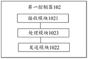
- the first controller 102 includes a receiving module 1021, a sending module 1022, and a processing module 1023.
- the processing module 1023 is connected to the receiving module 1021 and the sending module 1022, respectively.
- the receiving module 1021 is configured to receive a destination address sent by the shared cache device 104, where the destination address is used to indicate an address to be written to the shared cache device 104.
- the receiving module 1021 is further configured to receive information that carries the data.
- the processing module 1023 is configured to parse the information carrying the data to obtain the data.
- the sending module 1022 is configured to send the data and destination address to the shared cache device 104, instructing the shared cache device 104 to write data to the storage space pointed by the destination address.
- the first controller 102 may further include a control cache module 1024, and the control cache module 1024 is connected to the processing module 1023.
- the processing module 1023 stores the data to be written to the shared cache device 104 in the control cache module 1024.
- the sending module 1022 is further configured to send the source address and the destination address to the shared cache device 104, where the source address is an address of the data stored in the control cache module 1024.
- the shared cache device 104 reads the data from the control cache module 1024 based on the source address and writes the data into the storage space of the shared cache device 104 to which the destination address of the data points.
- the shared cache device 104 includes a transceiver module 1041, a processing module 1042, and a non-volatile cache module 1043.
- the processing module 1042 is respectively connected to the transceiver module 1041 and the non-volatile cache module 1043.
- the module 1041 is configured to send the destination address of the shared cache device 104 to the first controller 102, and is further configured to receive the data sent by the first controller 102, the destination address of the data, and the processing module 1023 is configured to determine that the transceiver module 1041 receives The destination address of the data is reached, and the data is stored in the storage space of the non-volatile cache module 1043 pointed to by the destination address.
- the shared cache device 104 further includes a shared memory 1044, which is connected to the processing module 1042.
- the processing module 1023 is configured to store the data in the shared memory 1044.
- the shared memory 1044 is stored. The data is written once in the storage space of the non-volatile cache module 1043 pointed to by the destination address.
- the shared memory 1044 is a dynamic random access memory (DRAM) storage medium.
- DRAM dynamic random access memory
- the backup can be configured in the shared cache device 104.
- the DRAM storage medium can be a supercapacitor.
- the shared memory 1044 can serve as a buffer storage medium for the non-volatile cache module 1043, thereby reducing the frequency of access to the non-volatile storage medium, thereby reducing the internals of the NVM storage medium. abrasion.
- the transceiver module 1041 in the shared cache device 104 may further include a first interface 1045 and a second interface 1046.
- the first controller 102 and the shared cache device 104 are connected by the first interface 1045 of the shared cache device 104, and the second controller 103 and the shared cache device 104 are connected by the second interface 1046 of the shared cache device 104.
- the first interface 1045 is configured to receive the data sent by the first controller 102, the destination address of the data, and send the data and the destination address of the data to the processing module 1042 in the shared cache device 104.
- the processing module 1042 The received data and the destination address of the data are processed, and the data needs to be stored in the storage space of the shared cache device 104 according to the destination address, and the data is stored in the non-volatile cache module 1043 pointed to by the destination address. In storage space.
- the method for accessing data provided by the embodiment of the present application is described below by taking the communication between the shared cache device 104 and the first controller 102 as an example.
- FIG. 7 is a schematic flowchart of a method for data access provided by an embodiment of the present application.
- step S201 in the method of method data access may be performed by the shared cache device 104 shown in FIG. 1 or FIG. 4 or FIG. 5, or may also be in the shared cache device 104 shown in FIG.
- the transceiver module 1041 performs;
- the step S202 in the method of data access may be performed by the first controller 102 or the second controller 103 shown in FIG. 1, or may also be performed by the receiving module 1021 shown in FIG. 2;
- Step S203 in the method of data access may be performed by the first controller 102 or the second controller 103 shown in FIG. 1, or may be performed by the transmitting module 1022 shown in FIG.
- the processing module 1023 and the sending module 1022 shown in FIG. 2 are executed in cooperation; the step S204 in the method of data accessing may be performed by the shared cache device 104 shown in FIG. 1 or FIG. 4 or FIG. 5, or may also be represented by The processing module 1041 of the shared cache device 104 shown in FIG. 5 executes. This embodiment of the present application does not specifically limit this.
- the shared cache device 104 sends a destination address to the first controller 102, where the destination address is used to indicate that the data is to be written to the address of the shared cache device 104.
- the first controller 102 maps the storage space pointed to by the destination address of the shared cache device 104 to the global storage space of the system according to the destination address, and stores the mapping relationship between the destination address and the logical address of the shared cache device 104.
- the logical address of the shared cache device 104 indicates the address layout of the storage space corresponding to the destination address of the shared cache device 104 in the global storage space of the storage system.
- the destination address includes the start address and the end address of the storage space pointed to by a contiguous physical address or the identity of the shared cache device 104.
- the storage space corresponding to the destination address is a storage space pointed by a continuous physical address.
- the shared cache device 104 sends the destination address to the first controller 102.
- the destination address includes the start address and the end address of the storage space of the shared cache device 104, and the first controller 102 is based on the start.
- the address and the termination address map the storage space of the shared cache device 104 to the global storage space of the system.
- the first controller 102 maps the storage space corresponding to the destination address of the shared cache device 104 to the global storage space of the storage system
- the first controller 102 creates a logical address of the shared cache device 104, and stores the logical address of the shared cache device 104 and Mapping of destination addresses.
- the destination address is the physical address of the storage space of the shared cache device 104.
- the physical address of the storage space of the shared cache device 104 is visible to each controller, and each controller can The storage process is performed using the physical address of the storage space of the shared cache device 104.
- the destination address includes a start address of 0G and a termination address of 128G.
- the first controller 102 maps the storage space corresponding to 0G to 128G to the global storage space of the system according to the destination address.
- the storage space of 0G to 128G of the shared cache device 104 is mapped by the first controller 102 to the storage space of 80G to 208G of the global storage space, which is the logical address of the shared cache device 104.
- the destination address includes the identifier of the shared cache device 104 and the storage capacity of the storage space of the shared cache device 104.
- the first controller 102 stores the shared cache device 104 according to the storage capacity of the storage space of the shared cache device 104. The space is mapped to the global storage space.
- the first controller 102 After the first controller 102 creates the mapping relationship between the logical address of the shared cache device 104 and the destination address of the shared cache device 104, the first controller 102 can pass the mapping relationship table to the basic of the first controller 102.
- the Basic Input Output System (BIOS) is configured to the shared cache device 104. As such, the address layout of the storage space of the shared cache device 104 in the global storage space of the storage system is visible to the shared cache device 104.
- BIOS Basic Input Output System
- the destination address includes the identifier of the shared cache device 104
- the identifier of the shared cache device 104 may be any one of the number of the shared cache device 104 or the communication address of the shared cache device 104. No particular limitation is imposed.
- the first controller 102 pre-stores the storage capacity of the shared cache device 104, and the first controller 102 can query the storage capacity of the pre-stored shared cache device 104 according to the identifier of the shared cache device 104, according to the storage capacity of the shared cache device 104. After the storage space of the shared cache device 104 is mapped to the global storage space, the mapping relationship between the identifier of the shared cache device 104 and the logical address is saved.
- the storage space information of the shared cache device 104 is obtained by the first controller 102 only by receiving the destination address sent by the shared cache device 104.
- the embodiments of the present application are not limited thereto.
- the first controller 102 can also acquire the destination address of the shared cache device 104 through the basic input output system (BIOS) of the first controller 102 when the system is powered on or restarted.
- BIOS basic input output system
- the first controller 102 receives information carrying data.
- the first controller 102 receives the information carrying the data sent by the host 101, where the data is data to be written into the shared cache device 104.
- the first controller 102 After receiving the information carrying the data, the first controller 102 parses the information carrying the data and acquires the data. The first controller 102 determines a logical address of the global storage space to be stored to the storage system, and determines the shared cache device 104 to be written according to the mapping relationship between the logical address and the identifier of the shared cache device 104. .
- the mapping relationship between the logical address of the shared cache device and the destination address of the shared cache device 104 is created.
- the first controller 102 can determine, according to the mapping relationship between the logical address of the shared cache device 104 and the destination address of the shared cache device 104, the storage space to which the data is to be stored to the destination address of the shared cache device 104.
- the storage space pointed to by the destination address of the shared cache device 104 is the storage space within the range of the start address and the end address.
- the first controller 102 first determines the logic of the data to be stored in the global storage space of the storage system according to the mapping relationship between the logical address of the shared cache device 104 and the destination address of the shared cache device 104 in step S201.
- the address is located between 80G and 208G, and the destination address of the shared cache device 104 to which the data is to be stored is determined according to the mapping relationship between the logical addresses 80G to 208G of the shared cache device 104 and the destination address 0G to 128G of the shared cache device 104.
- the storage space is a storage space in the range of 0G to 128G addresses of the shared cache device 104.
- the first controller 102 sends the destination address and the data to the shared cache device 104, so that the shared cache device 104 saves the data to the storage space pointed by the destination address.
- step S203 the first controller 102 sends information carrying the destination address to the shared cache device 104 to implement transmission of the destination address.
- the destination address includes a start address and a termination address of a storage space pointed to by a contiguous physical address, or an identifier of the shared cache device 104.
- the first controller 102 sends the destination address and the data, and also sends the effective length of the data to the shared cache device 104.
- the effective length of the data indicates the size of the storage space that the data needs to occupy to indicate the shared cache device 104.
- the effective length of the allocated data indicates the size of the storage space to store the data.
- the first controller 102 generates a write data instruction, where the write data instruction includes the data, a destination address of the data (eg, the destination address of the data is a storage space) The start address and the end address or the identifier of the shared cache device 104), the first controller 102 sends the write data command to the first shared cache device 104.
- the write data instruction includes the data, a destination address of the data (eg, the destination address of the data is a storage space) The start address and the end address or the identifier of the shared cache device 104), the first controller 102 sends the write data command to the first shared cache device 104.
- the first controller 102 may further generate a write data instruction, where the write data instruction includes the data, a destination address of the data (eg, the destination address of the data is a segment The start address of the storage space or the identifier of the shared cache device 104, and the effective length of the data, the first controller 102 sends the write data command to the first shared cache device 104.
- the write data instruction includes the data, a destination address of the data (eg, the destination address of the data is a segment The start address of the storage space or the identifier of the shared cache device 104, and the effective length of the data
- the first controller 102 sends the data to the shared cache device 104.
- the first controller 102 first saves the data to the control cache module 1021. And generating a write data instruction, the write data instruction including a source address and a destination address to be written into the shared cache device 104, the source address being a storage location of the data in the control cache module 1021, first control
- the device 102 sends the write data instruction to the shared cache device 104 to cause the shared cache device 104 to read the data from the control cache module 1021 according to the source address.
- the shared cache device 104 saves the data to the storage space pointed by the destination address.
- the shared cache device 104 After receiving the destination address and the data sent by the first controller 102, the shared cache device 104 saves the data to the storage space pointed to by the destination address.
- the shared cache device 104 saves the data to the storage space pointed by the destination address in the following four implementation methods.
- the shared cache device 104 determines that the received identifier of the shared cache device 104 is consistent with the self-storage identifier, and saves The data is to the shared cache device 104.
- the shared cache device 104 When the destination address of the data includes the start address and the termination address of the storage space pointed to by a consecutive physical address, the shared cache device 104 directly stores the data in the storage space of the shared cache device 104 indicated by the destination address.
- the shared cache device 104 If the destination address of the shared cache device 104 includes the start address and the end address of the storage space pointed to by a contiguous physical address, and the identifier of the shared cache device 104, the shared cache device 104 first determines the identifier and saves itself according to the identifier. When the identifiers are consistent, the data is directly stored in the storage space of the shared cache device 104 indicated by the destination address.
- step S201 if the first controller 102 passes the mapping relationship between the logical address of the shared cache device 104 and the destination address of the shared cache device 104 through the basic input/output system (Basic Input Output System, BIOS) of the first controller 102.
- BIOS Basic Input Output System
- BIOS Basic Input Output System
- the configuration is given to the shared cache device 104.
- the shared cache device 104 In the case where the destination address sent by the first controller 102 to the shared cache device 104 includes the identifier and logical address of the shared cache device 104, the shared cache device 104 first determines the identifier based on the identifier.
- mapping relationship table may be queried, the corresponding destination address is determined according to the logical address of the shared cache device 104, and the data is stored in the storage space pointed to by the destination address of the shared cache device 104.
- the destination address sent by the first controller 102 to the shared cache device 104 includes the identifier of the shared cache device 104, and the first controller 102 sends the destination address to the shared cache device 104, and also to the shared cache device. And transmitting the data to the logical address of the global storage space.
- the shared cache device 104 first determines, according to the identifier, that the identifier is consistent with the identifier saved by itself, the shared cache device 104 further uses the first controller 102 as the shared cache.
- mapping relationship between the logical address of the shared cache device 104 configured by the device 104 and the destination address of the shared cache device 104, determining an offset of the logical address of the data to be stored in the global storage space from the starting logical address, and Based on the offset, the physical address of the data to be stored to the shared cache device 104 is determined, and the data is ultimately stored in the storage space of the shared cache device 104 to which the physical address points.
- the foregoing starting logical address may be a starting logical address of the global storage space (for example, the starting logical address of the global storage space is 0G), or the starting logical address may also be the shared cache device 104.
- the destination address is mapped to the starting logical address after the global storage space (for example, the starting logical address after the destination address of the shared cache device 104 is mapped to the global storage space is 90G), which is not specifically limited in this application.
- the host 101 can be connected to multiple shared cache devices 104, and any two shared cache devices of the plurality of shared cache devices 104 form a mirror shared cache device. That is, the read and write access of the host 101 to one of the two shared cache devices may also occur between the host 101 and another shared cache device 104, so that the same data may be stored in the arbitrary two.
- One of the shared cache devices in the shared cache device 104 can be stored in another shared cache device 104 at the same time, avoiding the loss of the data due to the failure of one of the shared cache devices 104, that is, improving the data storage. Reliability.
- the two interfaces of one of the above shared cache devices 104 are connected to the first controller 102 and the second controller 103, respectively.
- the two interfaces of the other shared cache device 104 are also respectively connected to the first controller 102 and the second controller 103, that is, each controller is respectively connected to two interfaces, and the two interfaces are respectively One of the interfaces of the one of the shared cache devices 104 and one of the interfaces of the other shared cache device 104 described above.
- the first controller 102 passes the mapping relationship between the logical address of the shared cache device and the physical address of the shared cache device through the basic input/output system of the first controller 102.
- the (Basic Input Output System, BIOS) configuration is exemplified for the shared cache device 104, but the embodiment of the present application is not limited thereto.
- the first controller 102 can also send the mapping relationship table to the shared cache device 104 along with the information carrying the data.
- the embodiment of the present application provides a controller (for example, the first controller 102), and a schematic block diagram of the controller is shown in FIG. 2 to FIG. 3. For brevity, details are not described herein again. The operations performed by the respective modules shown in FIG. 2 to FIG. 3 will be described.
- the receiving module 1021 is configured to receive a destination address sent by each of the shared cache devices 104, where the destination address is used to indicate that the data is to be written to the address of the shared cache device 104.
- the receiving module 1021 is further configured to:
- the sending module 1022 is configured to:
- the destination address and the data are sent to the shared cache device 104 that sends the destination address, such that each of the shared cache devices 104 saves the data to a storage space pointed to by the destination address.
- controller 102 further includes:
- the processing module 1023 is configured to generate a write data instruction, where the write data instruction includes the data and the destination address;
- the sending module 1022 is further configured to:
- the write data command is sent to the shared cache device 104 that sent the destination address.
- controller 102 further includes a control cache module 1024, where the processing module 1023 is further configured to:
- the write data instruction including a source address and the destination address, where the source address is an address of the data stored in the control cache module 1024;
- the sending module 1022 is further configured to:
- processing module 1023 in the embodiment of the present invention may be implemented by a processor or a processor related circuit component
- the receiving module 1021 may be implemented by a receiver or a receiver related circuit component
- the sending module 1022 may be related by a transmitter or a transmitter. Circuit component implementation.
- the embodiment of the present application further provides a control device 300.
- the control device 300 includes a processor 310, a memory 320 and a transceiver 330.
- the memory 320 stores instructions or programs, and the memory 320 is also used to The operations performed by the control cache module 1024 in the above embodiment are executed, and the processor 330 is configured to execute instructions or programs stored in the memory 320.
- the processor 310 is configured to perform the operations performed by the processing module 1023 in the above embodiment
- the transceiver 330 is configured to perform the operations performed by the receiving module 1021 or the transmitting module 1022 in the above embodiment. .
- the embodiment of the present application provides a shared cache device 104.
- the schematic block diagram of the shared cache device 104 is shown in FIG. 4 to FIG. 6.
- the transceiver module 1041 is configured to send a destination address to the first controller 102, where the destination address is used to indicate that the data is to be written to the address of the shared cache device 104.
- the transceiver module 1041 is further configured to:
- the processing module 1042 is configured to save the data to a storage space pointed by the destination address.
- the transceiver module 1041 is further configured to:
- the write data instruction including the data and the destination address.
- the first controller includes a control cache module 1024, where the transceiver module 1041 is specifically configured to:
- the processing module 1042 is further configured to:
- the shared cache device 104 further includes a non-volatile cache module 1043, where the non-volatile cache module 1043 is composed of an NVM medium, and the non-volatile cache module 1043 is connected to the processing module 1042.
- the transceiver module 1041 is further configured to:
- the processing module 1042 is further configured to:
- the data is saved to the non-volatile cache module 1043, and the non-volatile cache module 1043 includes a storage space pointed to by the destination address.
- the device further includes a non-volatile cache module 1043 and a shared memory 1044.
- the non-volatile cache module 1043 is composed of an NVM medium, and the shared memory 1044 and the non-volatile cache module 1043 are respectively connected to the processing module 1042. ,
- the transceiver module 1041 is further configured to:
- the processing module 1042 is further configured to:
- the data in the shared memory 1044 is saved to the non-volatile cache module 1043, and the non-volatile cache module 1043 includes a storage space pointed by the destination address.
- processing module 1042 in the embodiment of the present invention may be implemented by a processor or a processor related circuit component
- transceiver module 1041 may be implemented by a transceiver or a transceiver related circuit component.
- the embodiment of the present application further provides a shared cache device 400, which includes a processor 410, a memory 420 and a transceiver 430, wherein the memory 420 stores instructions or programs, and the memory 420 further
- the processor 430 is configured to execute the instructions or programs stored in the memory 420.
- the processor 410 is configured to perform the operations performed by the processing module 1042 in the above embodiment
- the transceiver 430 is configured to perform the operations performed by the transceiver module 1041 in the above embodiment.
- the disclosed systems, devices, and methods may be implemented in other manners.
- the device embodiments described above are merely illustrative.
- the division of the unit is only a logical function division.
- there may be another division manner for example, multiple units or components may be combined or Can be integrated into another system, or some features can be ignored or not executed.
- the mutual coupling or direct coupling or communication connection shown or discussed may be an indirect coupling or communication connection through some interface, device or unit, and may be in an electrical, mechanical or other form.
- the units described as separate components may or may not be physically separated, and the components displayed as units may or may not be physical units, that is, may be located in one place, or may be distributed to multiple network units. Some or all of the units may be selected according to actual needs to achieve the purpose of the solution of the embodiment.
- each functional unit in each embodiment of the present application may be integrated into one processing unit, or each unit may exist physically separately, or two or more units may be integrated into one unit.
- the functions may be stored in a computer readable storage medium if implemented in the form of a software functional unit and sold or used as a standalone product.
- the technical solution of the present application which is essential or contributes to the prior art, or a part of the technical solution, may be embodied in the form of a software product, which is stored in a storage medium, including
- the instructions are used to cause a computer device (which may be a personal computer, server, or network device, etc.) to perform all or part of the steps of the methods described in various embodiments of the present application.
- the foregoing storage medium includes: a U disk, a mobile hard disk, a read-only memory (ROM), a random access memory (RAM), a magnetic disk, or an optical disk, and the like, which can store program codes. .
Landscapes
- Engineering & Computer Science (AREA)
- Theoretical Computer Science (AREA)
- Physics & Mathematics (AREA)
- General Engineering & Computer Science (AREA)
- General Physics & Mathematics (AREA)
- Human Computer Interaction (AREA)
- Software Systems (AREA)
- Computer Security & Cryptography (AREA)
- Memory System Of A Hierarchy Structure (AREA)
Priority Applications (2)
| Application Number | Priority Date | Filing Date | Title |
|---|---|---|---|
| EP18854866.3A EP3637242A4 (de) | 2017-09-11 | 2018-06-11 | Datenzugriffsverfahren und -vorrichtung |
| US16/743,139 US11119953B2 (en) | 2017-09-11 | 2020-01-15 | Data access method and apparatus for accessing shared cache in a memory access manner |
Applications Claiming Priority (2)
| Application Number | Priority Date | Filing Date | Title |
|---|---|---|---|
| CN201710813215.9A CN109491587B (zh) | 2017-09-11 | 2017-09-11 | 数据访问的方法及装置 |
| CN201710813215.9 | 2017-09-11 |
Related Child Applications (1)
| Application Number | Title | Priority Date | Filing Date |
|---|---|---|---|
| US16/743,139 Continuation US11119953B2 (en) | 2017-09-11 | 2020-01-15 | Data access method and apparatus for accessing shared cache in a memory access manner |
Publications (1)
| Publication Number | Publication Date |
|---|---|
| WO2019047579A1 true WO2019047579A1 (zh) | 2019-03-14 |
Family
ID=65633498
Family Applications (1)
| Application Number | Title | Priority Date | Filing Date |
|---|---|---|---|
| PCT/CN2018/090578 WO2019047579A1 (zh) | 2017-09-11 | 2018-06-11 | 数据访问的方法及装置 |
Country Status (4)
| Country | Link |
|---|---|
| US (1) | US11119953B2 (de) |
| EP (1) | EP3637242A4 (de) |
| CN (1) | CN109491587B (de) |
| WO (1) | WO2019047579A1 (de) |
Families Citing this family (8)
| Publication number | Priority date | Publication date | Assignee | Title |
|---|---|---|---|---|
| CN109976677A (zh) * | 2019-04-03 | 2019-07-05 | 山东超越数控电子股份有限公司 | 一种存储系统控制方法、存储系统控制装置及存储系统 |
| CN112783954B (zh) * | 2019-11-06 | 2024-04-05 | 北京金山云网络技术有限公司 | 数据访问方法、装置及服务器 |
| CN111177054B (zh) * | 2019-12-30 | 2021-09-03 | 京信网络系统股份有限公司 | 数据传输方法、装置、设备及存储介质 |
| US20210389976A1 (en) * | 2020-06-11 | 2021-12-16 | Capital One Services, Llc | Techniques to facilitate a migration process to cloud storage |
| CN113873049A (zh) * | 2020-06-30 | 2021-12-31 | 中兴通讯股份有限公司 | 基于网络报文的远程内存访问的方法、装置、设备及介质 |
| CN112328533A (zh) * | 2020-11-09 | 2021-02-05 | 哲库科技(上海)有限公司 | 多核处理系统及其核间通信方法、存储介质 |
| CN113986788A (zh) * | 2021-10-28 | 2022-01-28 | 昆仑芯(北京)科技有限公司 | 数据处理方法和装置、芯片、电子设备及介质 |
| CN116225986A (zh) * | 2021-12-02 | 2023-06-06 | 华为技术有限公司 | 一种存储系统、数据处理方法及装置 |
Citations (4)
| Publication number | Priority date | Publication date | Assignee | Title |
|---|---|---|---|---|
| CN1447257A (zh) * | 2002-04-09 | 2003-10-08 | 威盛电子股份有限公司 | 分布式共享内存系统数据维护方法 |
| CN102567227A (zh) * | 2012-01-13 | 2012-07-11 | 北京邦诺存储科技有限公司 | 共享缓存设备的双控制器存储系统和方法 |
| CN105991756A (zh) * | 2015-03-23 | 2016-10-05 | 富士施乐株式会社 | 传输装置、传输系统以及传输方法 |
| JP2016177751A (ja) * | 2015-03-23 | 2016-10-06 | 富士ゼロックス株式会社 | 転送装置、転送システムおよびプログラム |
Family Cites Families (10)
| Publication number | Priority date | Publication date | Assignee | Title |
|---|---|---|---|---|
| US6970977B2 (en) * | 2003-03-31 | 2005-11-29 | Bull Hn Information Systems Inc. | Equal access to prevent gateword dominance in a multiprocessor write-into-cache environment |
| WO2004107180A1 (ja) * | 2003-05-30 | 2004-12-09 | Fujitsu Limited | マルチプロセッサシステム |
| CN100489814C (zh) * | 2007-08-01 | 2009-05-20 | 杭州华三通信技术有限公司 | 一种共享缓存系统及实现方法 |
| US9208082B1 (en) * | 2012-03-23 | 2015-12-08 | David R. Cheriton | Hardware-supported per-process metadata tags |
| CN102693198B (zh) * | 2012-05-12 | 2015-03-25 | 北京忆恒创源科技有限公司 | Dma传输方法及系统 |
| CN103106048A (zh) * | 2013-01-30 | 2013-05-15 | 浪潮电子信息产业股份有限公司 | 一种多控多活的存储系统 |
| BR112016003843B1 (pt) * | 2014-09-15 | 2019-04-24 | Huawei Technologies Co., Ltd. | Método de processamento de solicitação de gravar dados e arranjo de armazenamento |
| US10013177B2 (en) * | 2015-04-20 | 2018-07-03 | Hewlett Packard Enterprise Development Lp | Low write amplification in solid state drive |
| JP6319607B2 (ja) | 2015-12-03 | 2018-05-09 | 華為技術有限公司Huawei Technologies Co.,Ltd. | データを書き込むようにソリッドステートディスクを制御するためのアレイコントローラ、ソリッドステートディスクおよび方法 |
| AU2015411096A1 (en) * | 2015-12-17 | 2017-07-06 | Huawei Technologies Co., Ltd. | Write request processing method, processor and computer |
-
2017
- 2017-09-11 CN CN201710813215.9A patent/CN109491587B/zh active Active
-
2018
- 2018-06-11 EP EP18854866.3A patent/EP3637242A4/de active Pending
- 2018-06-11 WO PCT/CN2018/090578 patent/WO2019047579A1/zh unknown
-
2020
- 2020-01-15 US US16/743,139 patent/US11119953B2/en active Active
Patent Citations (4)
| Publication number | Priority date | Publication date | Assignee | Title |
|---|---|---|---|---|
| CN1447257A (zh) * | 2002-04-09 | 2003-10-08 | 威盛电子股份有限公司 | 分布式共享内存系统数据维护方法 |
| CN102567227A (zh) * | 2012-01-13 | 2012-07-11 | 北京邦诺存储科技有限公司 | 共享缓存设备的双控制器存储系统和方法 |
| CN105991756A (zh) * | 2015-03-23 | 2016-10-05 | 富士施乐株式会社 | 传输装置、传输系统以及传输方法 |
| JP2016177751A (ja) * | 2015-03-23 | 2016-10-06 | 富士ゼロックス株式会社 | 転送装置、転送システムおよびプログラム |
Non-Patent Citations (1)
| Title |
|---|
| See also references of EP3637242A4 * |
Also Published As
| Publication number | Publication date |
|---|---|
| EP3637242A4 (de) | 2020-08-05 |
| CN109491587A (zh) | 2019-03-19 |
| US11119953B2 (en) | 2021-09-14 |
| CN109491587B (zh) | 2021-03-23 |
| US20200151122A1 (en) | 2020-05-14 |
| EP3637242A1 (de) | 2020-04-15 |
Similar Documents
| Publication | Publication Date | Title |
|---|---|---|
| WO2019047579A1 (zh) | 数据访问的方法及装置 | |
| US10002085B2 (en) | Peripheral component interconnect (PCI) device and system including the PCI | |
| USRE49273E1 (en) | Switch and memory device | |
| CN107241913B (zh) | 信息处理装置 | |
| US9619389B1 (en) | System for a backward and forward application environment compatible distributed shared coherent storage | |
| US11960749B2 (en) | Data migration method, host, and solid state disk | |
| US8156376B2 (en) | Method, device and system for storing data in cache in case of power failure | |
| US8966195B2 (en) | Direct memory access and super page swapping optimizations for a memory blade | |
| CN109791522B (zh) | 数据迁移的方法、系统及智能网卡 | |
| US20200104067A1 (en) | Method for fast boot read | |
| US11868285B2 (en) | Memory controller configured to transmit interrupt signal if volatile memory has no data corresponding to address requested from source | |
| US20140244949A1 (en) | Asynchronous Data Mirroring in Memory Controller | |
| US10152274B2 (en) | Method and apparatus for reading/writing data from/into flash memory, and user equipment | |
| US10657052B2 (en) | Information handling system with priority based cache flushing of flash dual in-line memory module pool | |
| US20150143028A1 (en) | Data storage apparatus and operating method thereof | |
| US10102125B2 (en) | PCI device, interface system including the same, and computing system including the same | |
| US9003129B1 (en) | Techniques for inter-storage-processor cache communication using tokens | |
| CN108519860B (zh) | 一种ssd读命中的处理方法和装置 | |
| US9740423B2 (en) | Computer system | |
| CN113031863B (zh) | Ssd命令相关性管理方法、装置、计算机设备及存储介质 | |
| US9836359B2 (en) | Storage and control method of the same | |
| US10191690B2 (en) | Storage system, control device, memory device, data access method, and program recording medium | |
| JP2011192053A (ja) | ディスクアレイ装置、ディスクアレイシステム、及びキャッシュ制御方法 | |
| CN114327248A (zh) | 存储节点、存储设备及网络芯片 | |
| US20190339875A9 (en) | Method, electronic device and computer program product for data processing |
Legal Events
| Date | Code | Title | Description |
|---|---|---|---|
| 121 | Ep: the epo has been informed by wipo that ep was designated in this application |
Ref document number: 18854866 Country of ref document: EP Kind code of ref document: A1 |
|
| ENP | Entry into the national phase |
Ref document number: 2018854866 Country of ref document: EP Effective date: 20200110 |
|
| NENP | Non-entry into the national phase |
Ref country code: DE |