WO2019044628A1 - 液晶表示装置 - Google Patents
液晶表示装置 Download PDFInfo
- Publication number
- WO2019044628A1 WO2019044628A1 PCT/JP2018/031012 JP2018031012W WO2019044628A1 WO 2019044628 A1 WO2019044628 A1 WO 2019044628A1 JP 2018031012 W JP2018031012 W JP 2018031012W WO 2019044628 A1 WO2019044628 A1 WO 2019044628A1
- Authority
- WO
- WIPO (PCT)
- Prior art keywords
- liquid crystal
- light
- display device
- crystal display
- wavelength
- Prior art date
- Legal status (The legal status is an assumption and is not a legal conclusion. Google has not performed a legal analysis and makes no representation as to the accuracy of the status listed.)
- Ceased
Links
Images


Classifications
-
- G—PHYSICS
- G02—OPTICS
- G02B—OPTICAL ELEMENTS, SYSTEMS OR APPARATUS
- G02B5/00—Optical elements other than lenses
- G02B5/20—Filters
-
- G—PHYSICS
- G02—OPTICS
- G02F—OPTICAL DEVICES OR ARRANGEMENTS FOR THE CONTROL OF LIGHT BY MODIFICATION OF THE OPTICAL PROPERTIES OF THE MEDIA OF THE ELEMENTS INVOLVED THEREIN; NON-LINEAR OPTICS; FREQUENCY-CHANGING OF LIGHT; OPTICAL LOGIC ELEMENTS; OPTICAL ANALOGUE/DIGITAL CONVERTERS
- G02F1/00—Devices or arrangements for the control of the intensity, colour, phase, polarisation or direction of light arriving from an independent light source, e.g. switching, gating or modulating; Non-linear optics
- G02F1/01—Devices or arrangements for the control of the intensity, colour, phase, polarisation or direction of light arriving from an independent light source, e.g. switching, gating or modulating; Non-linear optics for the control of the intensity, phase, polarisation or colour
- G02F1/13—Devices or arrangements for the control of the intensity, colour, phase, polarisation or direction of light arriving from an independent light source, e.g. switching, gating or modulating; Non-linear optics for the control of the intensity, phase, polarisation or colour based on liquid crystals, e.g. single liquid crystal display cells
- G02F1/133—Constructional arrangements; Operation of liquid crystal cells; Circuit arrangements
- G02F1/1333—Constructional arrangements; Manufacturing methods
- G02F1/1335—Structural association of cells with optical devices, e.g. polarisers or reflectors
-
- G—PHYSICS
- G02—OPTICS
- G02F—OPTICAL DEVICES OR ARRANGEMENTS FOR THE CONTROL OF LIGHT BY MODIFICATION OF THE OPTICAL PROPERTIES OF THE MEDIA OF THE ELEMENTS INVOLVED THEREIN; NON-LINEAR OPTICS; FREQUENCY-CHANGING OF LIGHT; OPTICAL LOGIC ELEMENTS; OPTICAL ANALOGUE/DIGITAL CONVERTERS
- G02F1/00—Devices or arrangements for the control of the intensity, colour, phase, polarisation or direction of light arriving from an independent light source, e.g. switching, gating or modulating; Non-linear optics
- G02F1/01—Devices or arrangements for the control of the intensity, colour, phase, polarisation or direction of light arriving from an independent light source, e.g. switching, gating or modulating; Non-linear optics for the control of the intensity, phase, polarisation or colour
- G02F1/13—Devices or arrangements for the control of the intensity, colour, phase, polarisation or direction of light arriving from an independent light source, e.g. switching, gating or modulating; Non-linear optics for the control of the intensity, phase, polarisation or colour based on liquid crystals, e.g. single liquid crystal display cells
- G02F1/137—Devices or arrangements for the control of the intensity, colour, phase, polarisation or direction of light arriving from an independent light source, e.g. switching, gating or modulating; Non-linear optics for the control of the intensity, phase, polarisation or colour based on liquid crystals, e.g. single liquid crystal display cells characterised by the electro-optical or magneto-optical effect, e.g. field-induced phase transition, orientation effect, guest-host interaction or dynamic scattering
- G02F1/139—Devices or arrangements for the control of the intensity, colour, phase, polarisation or direction of light arriving from an independent light source, e.g. switching, gating or modulating; Non-linear optics for the control of the intensity, phase, polarisation or colour based on liquid crystals, e.g. single liquid crystal display cells characterised by the electro-optical or magneto-optical effect, e.g. field-induced phase transition, orientation effect, guest-host interaction or dynamic scattering based on orientation effects in which the liquid crystal remains transparent
-
- G—PHYSICS
- G09—EDUCATION; CRYPTOGRAPHY; DISPLAY; ADVERTISING; SEALS
- G09F—DISPLAYING; ADVERTISING; SIGNS; LABELS OR NAME-PLATES; SEALS
- G09F9/00—Indicating arrangements for variable information in which the information is built-up on a support by selection or combination of individual elements
-
- G—PHYSICS
- G09—EDUCATION; CRYPTOGRAPHY; DISPLAY; ADVERTISING; SEALS
- G09F—DISPLAYING; ADVERTISING; SIGNS; LABELS OR NAME-PLATES; SEALS
- G09F9/00—Indicating arrangements for variable information in which the information is built-up on a support by selection or combination of individual elements
- G09F9/30—Indicating arrangements for variable information in which the information is built-up on a support by selection or combination of individual elements in which the desired character or characters are formed by combining individual elements
Definitions
- the present invention relates to a liquid crystal display device using quantum dots.
- a liquid crystal display device provided with a wavelength conversion layer (color filter layer) that converts the wavelength of light using quantum dots.
- a wavelength conversion layer color filter layer
- an in-cell polarizing plate in which a wire grid type polarizer is provided in a cell is used to control the amount of light to be incident on the wavelength conversion layer.
- the in-cell polarizing plate described in Patent Document 1 has a problem that the degree of polarization is smaller than that of a general iodine-based polarizing plate.
- the film of the wire grid polarizing plate prepared separately is attached to the inside of the cell, there are problems such as the thickness of the base film, dust biting, and the decrease in reliability due to the adhesive, which makes mass production difficult I have a problem.
- An object of one embodiment of the present invention is to realize a liquid crystal display device which can control the irradiation amount of light to the wavelength conversion layer with high accuracy and can be easily manufactured.
- a liquid crystal display device includes a light source unit for emitting monochromatic light, a pair of substrates, a liquid crystal layer sandwiched between the pair of substrates, and And a wavelength conversion unit for converting the wavelength of the circularly polarized light by quantum dots, wherein the liquid crystal layer is made of cholesteric liquid crystal and the voltage is not applied.
- the twisting pitch of the cholesteric liquid crystal is the same as or substantially the same as the wavelength of the monochromatic light.
- the present invention it is possible to control the irradiation amount of light to the wavelength conversion layer with high accuracy, and it is possible to easily manufacture a liquid crystal display device.
- Embodiment 1 the liquid crystal display device 1A as an embodiment of the present invention will be described in detail.
- the direction from the backlight unit of the liquid crystal display device to the display surface of the liquid crystal display device will be described as upward.
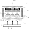
- FIG. 1 is a schematic cross-sectional view showing the configuration of the liquid crystal display device 1A.
- the liquid crystal display device 1A includes a backlight unit 10 (light source unit), a polarizing plate 2, a retardation plate 3, a first substrate 20, a liquid crystal layer 4, and a second substrate 30. Is equipped. Further, the liquid crystal display device 1A is provided between a first transparent substrate 21 to be described later and a second transparent substrate 31 to be described later, and includes a seal unit 5 which seals (seals) the liquid crystal layer 4.
- the backlight unit 10 includes a reflective plate 11, a blue light emitting element 12, a light guide plate 13, and an optical sheet 14.
- a light guide plate 13 having a blue light emitting element 12 at its end is formed on the upper surface of the reflection plate 11.
- the blue light emitting element 12 may be, for example, a blue LED that emits blue light having a peak wavelength of 450 nm.
- the blue light emitting element 12 projects blue light toward the inside of the light guide plate 13.
- the light guide plate 13 has a minute structure on each of the upper and lower surfaces thereof.
- the light guide plate 13 guides the light projected from the blue light emitting element 12 and emits the light from the above minute structure to the outside of the light guide plate 13.
- the blue light emitted from the lower surface of the light guide plate 13 is reflected by the reflection plate 11 and irradiated upward.
- the optical sheet 14 is provided on the upper surface of the light guide plate 13 and limits the spread angle of the blue light emitted from the light guide plate 13. Details will be described later.
- the polarizing plate 2 converts blue light emitted from the backlight unit 10 into linearly polarized light.
- the retardation plate 3 converts the light polarized into linearly polarized light by the polarizing plate 2 into circularly polarized light.
- the phase difference plate 3 has a phase difference of ⁇ / 4 between the phase of the wavelength of the extraordinary light and the phase of the wavelength of the normal light.
- the birefringence is set.
- the polarizing plate 2 and the retardation plate 3 function as a circularly polarizing portion that converts blue light into circularly polarized light.
- the retardation plate 3 is disposed on the lower surface of a first transparent substrate 21 described later.
- the polarizing plate 2 is disposed on the lower surface of the retardation plate 3.
- the first substrate 20 includes a first transparent substrate 21 (substrate), a pixel electrode 22, and a first liquid crystal alignment film 23.
- the first transparent substrate 21 is called an array substrate and has translucency.
- the blue light emitted from the backlight unit 10 is incident on the first transparent substrate 21 from a direction perpendicular to the first transparent substrate 21.
- the pixel electrode 22 is provided on the upper surface of the first transparent substrate 21 for each of the red color conversion portion 32A, the green color conversion portion 32B, and the blue light diffusion portion 32C of the wavelength conversion layer 32 described later.
- TFTs Thin Film Transistors
- the first liquid crystal alignment film 23 aligns the molecules of the liquid crystal of the liquid crystal layer 4 in a predetermined direction together with a second liquid crystal alignment film 34 described later, and is provided on the lower surface of the liquid crystal layer 4.
- the liquid crystal layer 4 is made of a cholesteric liquid crystal layer.
- the liquid crystal layer 4 is sandwiched between a pair of substrates (a first transparent substrate 21 and a second transparent substrate 31 described later).
- the liquid crystal layer 4 is formed by adding a large amount (specifically, 10 to several tens wt%) of a chiral dopant to a nematic liquid crystal having positive dielectric anisotropy.
- the rotational direction of the circularly polarized light polarized by the retardation plate 3 and the twisting direction of the cholesteric liquid crystal layer are in the same direction. Details will be described later.
- the second substrate 30 includes a second transparent substrate 31 (substrate), a wavelength conversion layer 32 (wavelength conversion unit), a counter electrode 33, and a second liquid crystal alignment film 34.
- the second transparent substrate 31 has translucency.
- the wavelength conversion layer 32 is formed on the lower surface of the second transparent substrate 31.
- the second transparent substrate 31 is disposed in parallel with the first transparent substrate 21.
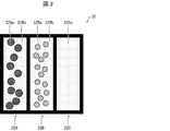
- FIG. 2 is a schematic view of the wavelength conversion layer 32.
- the wavelength conversion layer 32 includes a red color conversion unit 32A, a green color conversion unit 32B, and a blue light diffusion unit 32C.
- the wavelength conversion layer 32 may be provided with a spacer such as an overcoat layer or a photo spacer.
- the red converter 32A is formed by dispersing red fluorescent quantum dots 32Aa (quantum dots) for converting blue light into red light in the resin 32Ab.
- the blue light that has passed through the liquid crystal layer 4 and is incident on the red color conversion portion 32A is converted to red light by the red fluorescent quantum dot 32Aa and emitted from the upper surface of the red color conversion portion 32A.
- the green color conversion part 32B is formed by dispersing green fluorescent quantum dots 32Ba (quantum dots) for converting blue light into green light in the resin 32Bb.
- the blue light that has passed through the liquid crystal layer 4 and is incident on the green color conversion portion 32B is converted to green light by the green fluorescent quantum dots 32Ba and emitted from the upper surface of the green color conversion portion 32B.
- the blue light diffusion portion 32C includes a resin 32Ca that diffuses blue light.
- the blue light that has passed through the liquid crystal layer 4 and is incident on the blue light diffusion portion 32C is diffused by the resin 32Ca and emitted from the upper surface of the blue light diffusion portion 32C.
- FIGS. 1 and 2 show only one each of the red color conversion portion 32A, the green color conversion portion 32B, and the blue light diffusion portion 32C for the convenience of description.
- the liquid crystal display device 1A is provided with a plurality of red color conversion portions 32A, green color conversion portions 32B, and blue light diffusion portions 32C, and each red color conversion portion 32A, green color conversion portion 32B, and blue light diffusion portions
- the pixel electrode 22 is provided for 32C.
- the counter electrode 33 is provided on the lower surface of the wavelength conversion layer 32.
- a predetermined potential difference is provided between the pixel electrode 22 and the counter electrode 33 by controlling the potential of the pixel electrode 22 of the first substrate 20 and the potential of the counter electrode 33. Thereby, the alignment of the liquid crystal molecules in the liquid crystal layer 4 is controlled. Details will be described later.
- a second liquid crystal alignment film 34 is formed on the lower surface of the counter electrode 33.
- the liquid crystal layer 4 is made of cholesteric liquid crystal, and the axis of torsion is perpendicular to the first transparent substrate 21 when no voltage is applied between the pixel electrode 22 and the counter electrode 33. It is set to be When a voltage is not applied between the pixel electrode 22 and the counter electrode 33, the liquid crystal molecules of the liquid crystal layer 4 are parallel to the first transparent substrate 21 by the first liquid crystal alignment film 23 and the second liquid crystal alignment film 34. It is oriented. Further, the liquid crystal layer 4 is set so that the twisting pitch P when the voltage is not applied between the pixel electrode 22 and the counter electrode 33 becomes the same as the wavelength ⁇ of the blue light emitted from the backlight unit 10. It is done.
- Such setting includes (1) control of the alignment direction of liquid crystal molecules by the first liquid crystal alignment film 23 and the second liquid crystal alignment film 34, (2) control of the twist amount by the addition amount of the chiral dopant, and (3) This can be realized by controlling the thickness of the liquid crystal layer 4 in the vertical direction.
- the liquid crystal display device 1A light is not irradiated from a region where a voltage is not applied between the pixel electrode 22 and the counter electrode 33.
- the product of the twist pitch P of the liquid crystal layer 4 and the refractive index of the liquid crystal is the same as the wavelength of blue light (that is, when the above formula (1) is satisfied)
- blue light is produced by selective reflection by the liquid crystal layer 4 Can be completely reflected.
- the twist pitch P of the liquid crystal layer 4 is substantially the same as the wavelength of blue light (specifically, the product of the twist pitch P and the refractive index of the liquid crystal is 0. 0 of the wavelength of blue light. It is possible to cause selective reflection by the liquid crystal layer 4 to occur by 9 times to 1.1 times).
- the blue light that has reached the green color conversion portion 32B of the wavelength conversion layer 32 is wavelength converted to green light by the green color conversion portion 32B.
- the blue light that has reached the blue light diffusion portion 32C of the wavelength conversion layer 32 is diffused by the blue light diffusion portion 32C.
- the amount of blue light reaching the wavelength conversion layer 32 can be adjusted by controlling the voltage applied between the pixel electrode 22 and the counter electrode 33.
- the irradiation amount of the blue light to the wavelength conversion layer 32 can be controlled with high accuracy by the presence or absence of the potential difference between the pixel electrode 22 and the counter electrode 33 (in other words, Color reproduction range can be expanded). Further, since it is not necessary to provide a polarizing plate in the cell as in the prior art, the liquid crystal display device 1A can be easily manufactured. In other words, the liquid crystal display device 1A can be manufactured at a mass production level.
- the blue light emitting element 12 is preferably a light emitting element that emits light in a narrow wavelength range, such as a blue LED. Thereby, the display contrast can be enhanced.
- the twisting pitch P becomes 281 to 300 nm.
- the blue light emitting element 12 is a general blue LED
- the wavelength distribution of the emitted blue light is approximately in the range of 100 nm.
- the above-mentioned birefringence ⁇ n lc is a numerical value when light is irradiated from the backlight unit 10 in a direction perpendicular to the liquid crystal layer 4.
- the light from the backlight unit 10 is emitted to the liquid crystal layer 4 with a spread. Therefore, it is necessary to set the birefringence ⁇ n lc of the liquid crystal layer 4 in consideration of the spread.
- the incident angle of blue light to the liquid crystal layer 4 that is, the angle between the incident direction of blue light and the normal direction of the lower surface of the liquid crystal layer 4
- the birefringence is ⁇ n lc It needs to be / cos ⁇ .
- the backlight unit 10 is provided with the optical sheet 14, and the spread angle of blue light emitted from the backlight unit 10 (more specifically, the light guide plate 13) (in other words, emission angle) Is limited.
- the optical sheet 14 is designed such that the spread angle of the blue light emitted from the backlight unit 10 is 15 ° or less. Thereby, the display contrast can be enhanced.
- the birefringence ⁇ n lc of the liquid crystal layer 4 is preferably 0.1 or more and 0.5 or less.
- the twist pitch P of the cholesteric liquid crystal layer generally increases with the temperature rise. Therefore, it is difficult to keep the twist pitch P constant by the alignment control force by the liquid crystal alignment film provided on both sides of the cholesteric liquid crystal layer, and the number of twists may be different in the cell thickness direction. Therefore, it is preferable to substantially flatten the temperature dependency of the twisting pitch P by adding a plurality of chiral dopants different in the twisting direction in an appropriate amount combination. For example, by adding CB-15 (manufactured by BDH) and S-811 (manufactured by Merck) as a chiral dopant in combination, the temperature dependence of the twisting pitch P can be made substantially flat.
- the pretilt by the first liquid crystal alignment film 23 and the second liquid crystal alignment film 34 is relatively It is preferable to set a high value (specifically, 3 ° or more and 5 or less).
- the liquid crystal display device 1B in the present embodiment differs from the liquid crystal display device 1A in the first embodiment in the wavelength of light emitted from the backlight unit 10.
- FIG. 3 is a schematic cross-sectional view showing the configuration of the liquid crystal display device 1B.
- the liquid crystal display device 1 ⁇ / b> B includes a near ultraviolet light emitting element 40 for emitting near ultraviolet light, instead of the blue light emitting element 12 in the first embodiment.
- the liquid crystal display device 1B includes a wavelength conversion layer 41 in place of the wavelength conversion layer 32 in the first embodiment.
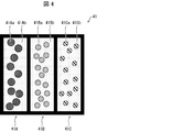
- FIG. 4 is a schematic view of the wavelength conversion layer 41. As shown in FIG.
- the wavelength conversion layer 41 includes a red color converter 41A, a green color converter 41B, and a blue color converter 41C.
- the red color conversion part 41A is formed by dispersing red fluorescent quantum dots 41Aa for converting near-ultraviolet light into red light in the resin 41Ab.
- the near-ultraviolet light that has passed through the liquid crystal layer 4 and is incident on the red color conversion portion 41A is converted to red light by the red fluorescent quantum dot 41Aa and emitted from the top surface of the red color conversion portion 41A.
- the green color conversion part 41B is formed by dispersing green fluorescent quantum dots 41Ba for converting near-ultraviolet light into green light in the resin 41Bb.
- the near-ultraviolet light that has passed through the liquid crystal layer 4 and is incident on the green color conversion part 41B is converted to green light by the green fluorescent quantum dots 41Ba and emitted from the upper surface of the green color conversion part 41B.
- the blue conversion part 41C is formed by dispersing blue fluorescent quantum dots 41Ca for converting near-ultraviolet light into blue light in a resin 41Cb.
- the near-ultraviolet light that has passed through the liquid crystal layer 4 and is incident on the blue conversion portion 41C is converted to blue light by the blue fluorescent quantum dot 41Ca, and is emitted from the upper surface of the blue conversion portion 41C.
- the near-ultraviolet light emitted from the backlight unit 10 and incident on the wavelength conversion layer 41 has its wavelength converted by the red conversion unit 41A, the green conversion unit 41B, or the blue conversion unit 41C.
- the viewing angle characteristics for each color become smaller, and the display quality can be improved.
- the liquid crystal display device 1C in the present embodiment is different from the liquid crystal display device 1A in the first embodiment in that laser light is emitted from the backlight unit 10.
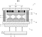
- FIG. 5 is a schematic cross-sectional view showing the configuration of the liquid crystal display device 1C.
- the liquid crystal display device 1 ⁇ / b> C includes a laser light emitting element 50 (light source) for emitting a laser light having a blue or near-ultraviolet wavelength instead of the blue light emitting element 12 in the first embodiment.
- the liquid crystal display device 1 ⁇ / b> C includes a wavelength conversion layer 51 in place of the wavelength conversion layer 32 in the first embodiment.
- FIG. 6 is a schematic view of the wavelength conversion layer 51. As shown in FIG.
- the wavelength conversion layer 51 as shown in FIG. 6, includes a red color conversion portion 51A, a green color conversion portion 51B, and a blue color conversion portion 51C.
- the red color conversion portion 51A is formed by dispersing red fluorescent quantum dots 51Aa for converting laser light into red light in the resin 51Ab.
- the laser light that has passed through the liquid crystal layer 4 and is incident on the red color conversion portion 51A is converted to red light by the red fluorescent quantum dot 51Aa, and is emitted from the upper surface of the red color conversion portion 51A.
- the green color conversion portion 51B is formed by dispersing green fluorescent quantum dots 51Ba for converting laser light into green light in the resin 51Bb.
- the laser light that has passed through the liquid crystal layer 4 and is incident on the green color conversion part 51B is converted to green light by the green fluorescent quantum dots 51Ba and emitted from the upper surface of the green color conversion part 51B.
- the blue conversion portion 51C is formed by dispersing blue fluorescent quantum dots 51Ca for converting laser light into blue light in the resin 51Cb.
- the laser light which has passed through the liquid crystal layer 4 and is incident on the blue conversion portion 51C is converted into blue light by the blue fluorescent quantum dot 51Ca, and is emitted from the upper surface of the blue conversion portion 51C.
- the wavelength of the laser light emitted from the backlight unit 10 and incident on the wavelength conversion layer 41 is converted by the red conversion unit 41A, the green conversion unit 41B, or the blue conversion unit 41C.
- the laser light is a monochromatic light having a very narrow wavelength range, so that all the laser light can be reflected by the liquid crystal layer 4 at the selective reflection by the liquid crystal layer 4. In other words, light does not leak during selective reflection.
- the display contrast can be made extremely large (in theory, it becomes infinite and virtually the same as a self-emitting device).
- a liquid crystal display (1A to 1C) comprises a light source unit (backlight unit 10) for emitting monochromatic light, a pair of substrates (first transparent substrate 21 and second transparent substrate 31), A liquid crystal layer 4 sandwiched between the pair of substrates, a circularly polarized portion (polarizing plate 2 and retardation plate 3) for converting the monochromatic light into circularly polarized light, and wavelength conversion of the circularly polarized light by quantum dots And a wavelength conversion portion (wavelength conversion layers 32, 41, 51), wherein the liquid crystal layer is made of cholesteric liquid crystal, and the twisting pitch P of the cholesteric liquid crystal is the same as the wavelength of the monochromatic light when voltage is not applied. Or substantially identical.
- the twist pitch of the liquid crystal layer (cholesteric liquid crystal) is the same as or substantially the same as the wavelength of monochromatic light.
- the twist pitch of the cholesteric liquid crystal becomes long, so that monochromatic light can reach the wavelength conversion portion. That is, according to the presence or absence of the application of the voltage to a liquid crystal layer, the irradiation amount of the monochromatic light to a wavelength conversion part can be controlled with high precision.
- the liquid crystal display can be easily manufactured. In other words, the liquid crystal display can be manufactured at a mass production level.
- the light source unit preferably includes an optical sheet 14 that limits the spread of the emission angle of the monochromatic light.
- the birefringence of the liquid crystal layer can be reduced.
- the amount of chiral dopant added to the nematic liquid crystal can be reduced.
- the optical sheet preferably has a configuration in which the spread of the emission angle of the monochromatic light is limited to 15 ° or less.
- the birefringence of the liquid crystal layer is preferably 0.1 or more. Thereby, the reflection bandwidth of monochromatic light in selective reflection can be increased.
- the light source unit includes a laser light emitting element 50 as a light source.
- the wavelength band of the laser light is an extremely narrow monochromatic light
- all the laser light can be reflected by the liquid crystal layer at the selective reflection by the liquid crystal layer.
- light does not leak during selective reflection.
- the display contrast can be made extremely large.
- Liquid Crystal Display Device 1A to 1C Liquid Crystal Display Device 2 Polarizing Plate (Circular Polarization Section) 3 Retardation plate (circularly polarized light) 4 liquid crystal layer 10 back light unit (light source unit) 14 Optical Sheet 21 First Transparent Substrate (Substrate) 31 Second transparent substrate (substrate) 32, 41, 51 wavelength conversion layer (wavelength converter) 50 laser light emitting elements
Landscapes
- Physics & Mathematics (AREA)
- General Physics & Mathematics (AREA)
- Nonlinear Science (AREA)
- Optics & Photonics (AREA)
- Engineering & Computer Science (AREA)
- Theoretical Computer Science (AREA)
- Chemical & Material Sciences (AREA)
- Crystallography & Structural Chemistry (AREA)
- Liquid Crystal (AREA)
- Mathematical Physics (AREA)
Abstract
波長変換層への光の照射量を高精度に制御し、かつ、液晶表示装置を簡易に製造する。液晶表示装置(1A)は、青色光を出射するバックライトユニット(10)と、第1透明基板(21)および第2透明基板(31)の間に挟持され、コレステリック液晶からなる液晶層(4)と、青色光を円偏光に変換する偏光板(2)および位相差板(3)と、円偏光の波長を量子ドットにより変換する波長変換層(32)とを備える。電圧が印加されていないときにおけるコレステリック液晶の捩れピッチは、青色光の波長と同一または実質的に同一である。
Description
本発明は、量子ドットを用いた液晶表示装置に関する。
量子ドットを用いて光の波長を変換する波長変換層(カラーフィルタ層)を備える液晶表示装置が知られている。このような液晶表示装置では、波長変換層に入射させる光の量を制御する必要がある。例えば、特許文献1には、セル内にワイヤグリッドタイプの偏光子を設けたインセル偏光板を用いて、波長変換層に入射させる光の量を制御している。
しかしながら、特許文献1に記載のインセル偏光板は、偏光度が一般的なヨウ素系偏光板と比較して小さいという問題がある。また、別途作成したワイヤグリッド偏光板のフィルムをセル内に貼り付けるため、ベースフィルムの厚み、ダスト噛み込み、および接着剤による信頼性の低下などの問題があり、量産することが困難であるという問題を有している。
本発明の一態様は、波長変換層への光の照射量を高精度に制御することができ、かつ、簡易に製造することができる液晶表示装置を実現することを目的とする。
上記の課題を解決するために、本発明の一態様に係る液晶表示装置は、単色光を出射する光源ユニットと、一対の基板と、前記一対の基板の間に挟持された液晶層と、前記単色光を円偏光に変換する円偏光部と、前記円偏光の波長を量子ドットにより変換する波長変換部とを備え、前記液晶層は、コレステリック液晶からなり、電圧が印加されていないときに前記コレステリック液晶の捩れピッチが前記単色光の波長と同一または実質的に同一である。
本発明の一態様によれば、波長変換層への光の照射量を高精度に制御することができ、かつ、液晶表示装置を簡易に製造することができるという効果を奏する。
〔実施形態1〕
以下、本発明の一実施形態としての液晶表示装置1Aについて、詳細に説明する。なお、本明細書では、液晶表示装置のバックライトユニットから、液晶表示装置の表示面に向かう方向を上方向として説明する。
以下、本発明の一実施形態としての液晶表示装置1Aについて、詳細に説明する。なお、本明細書では、液晶表示装置のバックライトユニットから、液晶表示装置の表示面に向かう方向を上方向として説明する。
(液晶表示装置1の概略構成)
図1は、液晶表示装置1Aの構成を示す概略断面図である。図1に示すように、液晶表示装置1Aは、バックライトユニット10(光源ユニット)と、偏光板2と、位相差板3と、第1基板20と、液晶層4と、第2基板30とを備えている。また、液晶表示装置1Aは、後述する第1透明基板21と後述する第2透明基板31との間に設置され、液晶層4をシール(密封)するシール部5を備えている。
図1は、液晶表示装置1Aの構成を示す概略断面図である。図1に示すように、液晶表示装置1Aは、バックライトユニット10(光源ユニット)と、偏光板2と、位相差板3と、第1基板20と、液晶層4と、第2基板30とを備えている。また、液晶表示装置1Aは、後述する第1透明基板21と後述する第2透明基板31との間に設置され、液晶層4をシール(密封)するシール部5を備えている。
バックライトユニット10は、反射板11と、青色発光素子12と、導光板13と、光学シート14とを備える。反射板11の上面には端部に青色発光素子12を備えた導光板13が形成されている。青色発光素子12は、例えば、ピーク波長が450nmの青色光を発行する青色LEDであってもよい。青色発光素子12は、導光板13の内部に向けて青色光を投射する。
導光板13は、その上下面それぞれに微小構造を有している。導光板13は、青色発光素子12から投射された光を導光し、上記微小構造から導光板13の外部へ向けて出射する。なお、導光板13の下面から放射された青色光は、反射板11において反射し、上方向へ照射される。
光学シート14は、導光板13の上面に設けられており、導光板13から出射される青色光の広がり角を制限する。詳細については、後述する。
偏光板2は、バックライトユニット10から出射された青色光を直線偏光に変換する。
位相差板3は、偏光板2によって直線偏光に偏光された光を、円偏光に変換する。位相差板3は、バックライトユニット10から照射される青色光の波長をλとしたときに、異常光の波長の位相と正常光の波長の位相との位相差がλ/4となるように複屈折率が設定されている。具体的には、位相差板3は、正常光の屈折率と異常光の屈折率との差をΔnr、位相差板3の厚みをdとしたときに、Δnr×d=λ/4となるように設定されている。偏光板2および位相差板3は、青色光を円偏光に変換する円偏光部として機能する。位相差板3は、後述する第1透明基板21の下面に設置されている。偏光板2は、位相差板3の下面に設置されている。
第1基板20は、第1透明基板21(基板)と、画素電極22と、第1液晶配向膜23とを備えている。
第1透明基板21は、アレイ基板と呼ばれ、透光性を有している。バックライトユニット10から照射された青色光は、第1透明基板21に対して垂直な方向から第1透明基板21に入射する。第1透明基板21の上面には、後述する波長変換層32の、赤色変換部32A、緑色変換部32B、および青色光拡散部32Cのそれぞれに対して画素電極22が設けられている。第1透明基板21には、画素電極22からの配線の交点にTFT(Thin Film Transistor)が配置されており、各画素電極22に電位を与えることができるようになっている。
第1液晶配向膜23は、後述する第2液晶配向膜34とともに、液晶層4の液晶の分子を一定方向に並べるものであり、液晶層4の下面に設けられている。
液晶層4は、コレステリック液晶層からなっている。液晶層4は、一対の基板(第1透明基板21、および後述する第2透明基板31)との間に挟持されている。液晶層4は、正の誘電率異方性を有するネマティック液晶にカイラルドーパントを多量(具体的には、10~数十wt%)に添加することにより形成される。位相差板3によって偏光された円偏光の回転方向と、コレステリック液晶層の捩れ方向は同一方向になっている。詳細については、後述する。
第2基板30は、第2透明基板31(基板)と、波長変換層32(波長変換部)と、対向電極33と、第2液晶配向膜34とを備えている。
第2透明基板31は、透光性を有している。第2透明基板31の下面には、波長変換層32が形成されている。第2透明基板31は、第1透明基板21と平行に配置されている。
図2は、波長変換層32の模式図である。波長変換層32は、図2に示すように、赤色変換部32Aと、緑色変換部32Bと、青色光拡散部32Cとを備えている。なお、図示していないが、波長変換層32に、オーバーコート層、フォトスペーサなどのスペーサを設けてもよい。
赤色変換部32Aは、青色光を赤色光に変換する赤色蛍光量子ドット32Aa(量子ドット)が樹脂32Ab中に分散されて形成されている。液晶層4を通過し赤色変換部32Aに入射した青色光は、赤色蛍光量子ドット32Aaにより赤色光に変換されて、赤色変換部32Aの上面から出射される。
緑色変換部32Bは、青色光を緑色光に変換する緑色蛍光量子ドット32Ba(量子ドット)が樹脂32Bb中に分散されて形成されている。液晶層4を通過し緑色変換部32Bに入射した青色光は、緑色蛍光量子ドット32Baにより緑色光に変換されて、緑色変換部32Bの上面から出射される。
青色光拡散部32Cは、青色光を拡散する樹脂32Caを備えている。液晶層4を通過し青色光拡散部32Cに入射した青色光は、樹脂32Caによって拡散されて、青色光拡散部32Cの上面から出射される。
なお、図1および図2には、説明の便宜上、赤色変換部32A、緑色変換部32B、および青色光拡散部32Cをそれぞれ1つずつのみ示している。実際には、液晶表示装置1Aは、赤色変換部32A、緑色変換部32B、および青色光拡散部32Cをそれぞれ複数備えており、それぞれの赤色変換部32A、緑色変換部32B、および青色光拡散部32Cに対して、画素電極22が設けられている。
対向電極33は、波長変換層32の下面に設けられている。液晶表示装置1Aでは、第1基板20の画素電極22の電位と、対向電極33の電位とを制御することにより、画素電極22と対向電極33との間に所定の電位差を与える。これにより、液晶層4の液晶分子の配向を制御する。詳細については、後述する。対向電極33の下面には、第2液晶配向膜34が形成されている。
(液晶表示装置1Aの動作)
次に、液晶表示装置1Aの動作について説明する。まず、液晶層4の詳細について説明する。
次に、液晶表示装置1Aの動作について説明する。まず、液晶層4の詳細について説明する。
上述したように、液晶層4は、コレステリック液晶からなっており、画素電極22と対向電極33との間に電圧が印加されていない場合において、捩れの軸が第1透明基板21に対して垂直となるように設定されている。画素電極22と対向電極33との間に電圧が印加されていない場合、液晶層4の液晶分子は、第1液晶配向膜23および第2液晶配向膜34により、第1透明基板21に平行に配向される。また、液晶層4は、画素電極22と対向電極33との間に電圧が印加されていない場合における捩れピッチPがバックライトユニット10から照射される青色光の波長λと同一となるように設定されている。すなわち、液晶層4の平均屈折率(配向ベクトルに平行な方向の屈折率と垂直な方向の屈折率との平均値)をnlcとしたとき、液晶層4は、下記の式(1)を満たすように設定されている。
nlc×P=λ・・・(1)
このような設定は、(1)第1液晶配向膜23および第2液晶配向膜34による液晶分子の配向方向の制御、(2)上記カイラルドーパントの添加量による捩れ量の制御、および(3)液晶層4の上下方向の厚みの制御により実現可能である。
nlc×P=λ・・・(1)
このような設定は、(1)第1液晶配向膜23および第2液晶配向膜34による液晶分子の配向方向の制御、(2)上記カイラルドーパントの添加量による捩れ量の制御、および(3)液晶層4の上下方向の厚みの制御により実現可能である。
次に、下記の(i)および(ii)に場合分けして液晶表示装置1Aの動作について説明する。
(i)画素電極22と対向電極33との間に電圧が印加されていない場合
上述したように、液晶表示装置1Aは、画素電極22と対向電極33との間に電圧が印加されていない場合、液晶層4の液晶分子が第1透明基板21に平行に配向されており、かつ、液晶層4が上記の式(1)を満たすように設定されている。そのため、画素電極22と対向電極33との間に電圧が印加されていない場合、位相差板3により円偏光に変換された青色光は、液晶層4の液晶分子によって反射される(この反射は、一般的に選択反射と呼ばれる)。これにより、画素電極22と対向電極33との間に電圧が印加されていない領域では、青色光が波長変換層32に到達しない。すなわち、液晶表示装置1Aでは、画素電極22と対向電極33との間に電圧が印加されていない領域からは光が照射されないようになっている。なお、液晶層4の捩れピッチPと液晶の屈折率との積が青色光の波長と同一である(すなわち、上記式(1)を満たす場合)には、液晶層4による選択反射によって青色光を完全に反射させることができる。しかし、実用上は、液晶層4の捩れピッチPが青色光の波長と実質的に同一である(具体的には、捩れピッチPと液晶の屈折率との積が青色光の波長の0.9倍~1.1倍である)ことにより、液晶層4による選択反射が起こるようにすることができる。
上述したように、液晶表示装置1Aは、画素電極22と対向電極33との間に電圧が印加されていない場合、液晶層4の液晶分子が第1透明基板21に平行に配向されており、かつ、液晶層4が上記の式(1)を満たすように設定されている。そのため、画素電極22と対向電極33との間に電圧が印加されていない場合、位相差板3により円偏光に変換された青色光は、液晶層4の液晶分子によって反射される(この反射は、一般的に選択反射と呼ばれる)。これにより、画素電極22と対向電極33との間に電圧が印加されていない領域では、青色光が波長変換層32に到達しない。すなわち、液晶表示装置1Aでは、画素電極22と対向電極33との間に電圧が印加されていない領域からは光が照射されないようになっている。なお、液晶層4の捩れピッチPと液晶の屈折率との積が青色光の波長と同一である(すなわち、上記式(1)を満たす場合)には、液晶層4による選択反射によって青色光を完全に反射させることができる。しかし、実用上は、液晶層4の捩れピッチPが青色光の波長と実質的に同一である(具体的には、捩れピッチPと液晶の屈折率との積が青色光の波長の0.9倍~1.1倍である)ことにより、液晶層4による選択反射が起こるようにすることができる。
(ii)画素電極22と対向電極33との間に電圧が印加されている場合
画素電極22と対向電極33との間に電圧が印加されると、液晶層4の液晶分子が第1透明基板21に対して垂直な方向に配向する。これにより、液晶層4の捩れピッチPが変化し、捩れピッチPが長くなった状態になる。そのため、上述した選択反射が起こらず、位相差版により円偏光に変換された青色光は、波長変換層32に到達する。例えば、波長変換層32の赤色変換部32Aに到達した青色光は、赤色変換部32Aによって赤色光に波長変換される。また、波長変換層32の緑色変換部32Bに到達した青色光は、緑色変換部32Bによって緑色光に波長変換される。また、波長変換層32の青色光拡散部32Cに到達した青色光は、青色光拡散部32Cによって拡散される。なお、画素電極22と対向電極33との間に印加する電圧を制御することにより、波長変換層32に到達する青色光の量を調整することができる。
画素電極22と対向電極33との間に電圧が印加されると、液晶層4の液晶分子が第1透明基板21に対して垂直な方向に配向する。これにより、液晶層4の捩れピッチPが変化し、捩れピッチPが長くなった状態になる。そのため、上述した選択反射が起こらず、位相差版により円偏光に変換された青色光は、波長変換層32に到達する。例えば、波長変換層32の赤色変換部32Aに到達した青色光は、赤色変換部32Aによって赤色光に波長変換される。また、波長変換層32の緑色変換部32Bに到達した青色光は、緑色変換部32Bによって緑色光に波長変換される。また、波長変換層32の青色光拡散部32Cに到達した青色光は、青色光拡散部32Cによって拡散される。なお、画素電極22と対向電極33との間に印加する電圧を制御することにより、波長変換層32に到達する青色光の量を調整することができる。
以上のように、液晶表示装置1Aでは、画素電極22と対向電極33との間の電位差の有無によって、波長変換層32への青色光の照射量を高精度に制御することができる(換言すれば、色再現範囲を広くすることができる)。また、従来のようにセル内に偏光板を設ける必要がないので、液晶表示装置1Aを簡易に製造できる、換言すれば、液晶表示装置1Aを量産レベルで製造することができる。
なお、液晶層4による光の選択反射は光の波長に依存する。そのため、バックライトユニット10から出射される光の波長分布をできるだけ小さくすることが好ましい。そのため、青色発光素子12は、青色LEDのような狭い波長域で発光する発光素子であることが好ましい。これにより、表示コントラストを高めることができる。
また、液晶層4によって光を選択反射するためには、液晶層4に入射する光は、液晶層4に対して垂直な方向(すなわち、上下方向)にできるだけ平行にする必要がある。
選択反射が起こる反射帯域幅をΔλ、液晶層4の複屈折率Δnlcとした場合、下記の式(2)が成り立つ。
Δλ=Δnlc/P・・・(2)
式(2)から、液晶層4の複屈折率Δnlcが大きいほど反射帯域幅を大きくできることがわかる。
Δλ=Δnlc/P・・・(2)
式(2)から、液晶層4の複屈折率Δnlcが大きいほど反射帯域幅を大きくできることがわかる。
ここで、青色発光素子12から出射される青色光の波長の中央値を450nmとし、液晶層4の平均屈折率nlcを一般的な値である1.5~1.6とした場合、上記の式(1)から捩れピッチPは281~300nmとなる。また、青色発光素子12が一般的な青色LEDである場合、出射される青色光の波長分布は、ほぼ100nmの範囲に収まっている。これらの条件を上記の式(2)に適用すると、100nmの範囲の反射帯域幅を得るためには、液晶層4の複屈折率Δnlcを0.28~0.3に設定する必要がある。
ただし、上記の複屈折率Δnlcはバックライトユニット10から液晶層4に対して垂直な方向に光が照射された場合の数値である。実際には、バックライトユニット10からの光は、広がりを持って液晶層4に照射される。そのため、当該広がりを考慮して液晶層4の複屈折率Δnlcを設定する必要がある。具体的には、液晶層4への青色光の入射角度(すなわち、青色光の入射方向と液晶層4の下面の法線方向とのなす角度)をθとした場合、複屈折率をΔnlc/cosθにする必要がある。しかしながら、複屈折率Δnlcを大きくするためには、ネマティック液晶に添加するカイラルドーパントを多くする必要があり、実用上困難となってしまう。そのため、液晶表示装置1Aでは、バックライトユニット10に光学シート14を設け、バックライトユニット10(より詳細には、導光板13)から出射される青色光の広がり角(換言すれば、出射角度)を制限している。具体的には、cosθの値を約0.035程度に抑えるため、光学シート14は、バックライトユニット10から出射される青色光の広がり角が15°以下になるように設計されている。これにより、表示コントラストを高めることができる。
また、上述したように、液晶層4の複屈折率Δnlcが大きいほど反射帯域幅を大きくすることができるが、応答速度および信頼性の面の問題が発生する可能性がある。そのため、液晶層4の複屈折率Δnlcは、0.1以上、かつ、0.5以下であることが好ましい。
また、コレステリック液晶層の捩れピッチPは、一般的に温度上昇とともに長くなる。そのため、コレステリック液晶層の両面に設置される液晶配向膜による配向規制力で捩れピッチPを一定に保つことが困難であり、セル厚方向において捩れ回数が違ってくる場合がある。そこで、捩れ方向の異なる複数のカイラルドーパントを適切な量の組み合わせで添加することにより、捩れピッチPの温度依存性をほぼフラットにすることが好ましい。例えば、カイラルドーパントとしてCB-15(BDH製)とS-811(Merck製)とを組み合わせて添加することにより、捩れピッチPの温度依存性をほぼフラットにすることができる。また、捩れ回数が設計したものとする(少なくとも、捩れ回数が設計した捩れ回数と半周分以下の差にする)ために、第1液晶配向膜23および第2液晶配向膜34によるプレティルトを比較的高い値(具体的には3°以上5以下)にすることが好ましい。
〔実施形態2〕
本発明の他の実施形態について、以下に説明する。なお、説明の便宜上、上記実施形態にて説明した部材と同じ機能を有する部材については、同じ符号を付記し、その説明を省略する。
本発明の他の実施形態について、以下に説明する。なお、説明の便宜上、上記実施形態にて説明した部材と同じ機能を有する部材については、同じ符号を付記し、その説明を省略する。
本実施形態における液晶表示装置1Bは、バックライトユニット10から照射される光の波長が実施形態1における液晶表示装置1Aと異なっている。
図3は、液晶表示装置1Bの構成を示す概略断面図である。図3に示すように、液晶表示装置1Bは、実施形態1における青色発光素子12に代えて、近紫外光を照射する近紫外光発光素子40を備えている。また、液晶表示装置1Bは、実施形態1における波長変換層32に代えて、波長変換層41を備えている。
図4は、波長変換層41の模式図である。波長変換層41は、図4に示すように、赤色変換部41Aと、緑色変換部41Bと、青色変換部41Cとを備えている。
赤色変換部41Aは、近紫外光を赤色光に変換する赤色蛍光量子ドット41Aaが樹脂41Ab中に分散されて形成されている。液晶層4を通過し赤色変換部41Aに入射した近紫外光は、赤色蛍光量子ドット41Aaにより赤色光に変換されて、赤色変換部41Aの上面から出射される。
緑色変換部41Bは、近紫外光を緑色光に変換する緑色蛍光量子ドット41Baが樹脂41Bb中に分散されて形成されている。液晶層4を通過し緑色変換部41Bに入射した近紫外光は、緑色蛍光量子ドット41Baにより緑色光に変換されて、緑色変換部41Bの上面から出射される。
青色変換部41Cは、近紫外光を青色光に変換する青色蛍光量子ドット41Caが樹脂41Cb中に分散されて形成されている。液晶層4を通過し青色変換部41Cに入射した近紫外光は、青色蛍光量子ドット41Caにより青色光に変換されて、青色変換部41Cの上面から出射される。
液晶表示装置1Bでは、バックライトユニット10から照射され、波長変換層41に入射した近紫外光は、赤色変換部41A、緑色変換部41B、または青色変換部41Cによって波長が変換される。これにより、実施形態1の液晶表示装置1Aに比べて、色ごとの視角特性が小さくなり、表示品位を向上させることができるようになっている。
〔実施形態3〕
本発明の他の実施形態について、以下に説明する。なお、説明の便宜上、上記実施形態にて説明した部材と同じ機能を有する部材については、同じ符号を付記し、その説明を省略する。
本発明の他の実施形態について、以下に説明する。なお、説明の便宜上、上記実施形態にて説明した部材と同じ機能を有する部材については、同じ符号を付記し、その説明を省略する。
本実施形態における液晶表示装置1Cは、バックライトユニット10からレーザ光を照射する点が実施形態1における液晶表示装置1Aと異なっている。
図5は、液晶表示装置1Cの構成を示す概略断面図である。図5に示すように、液晶表示装置1Cは、実施形態1における青色発光素子12に代えて、青色または近紫外の波長を有するレーザ光を照射するレーザ光発光素子50(光源)を備えている。また、液晶表示装置1Cは、実施形態1における波長変換層32に代えて、波長変換層51を備えている。
図6は、波長変換層51の模式図である。波長変換層51は、図6に示すように、赤色変換部51Aと、緑色変換部51Bと、青色変換部51Cとを備えている。
赤色変換部51Aは、レーザ光を赤色光に変換する赤色蛍光量子ドット51Aaが樹脂51Ab中に分散されて形成されている。液晶層4を通過し赤色変換部51Aに入射したレーザ光は、赤色蛍光量子ドット51Aaにより赤色光に変換されて、赤色変換部51Aの上面から出射される。
緑色変換部51Bは、レーザ光を緑色光に変換する緑色蛍光量子ドット51Baが樹脂51Bb中に分散されて形成されている。液晶層4を通過し緑色変換部51Bに入射したレーザ光は、緑色蛍光量子ドット51Baにより緑色光に変換されて、緑色変換部51Bの上面から出射される。
青色変換部51Cは、レーザ光を青色光に変換する青色蛍光量子ドット51Caが樹脂51Cb中に分散されて形成されている。液晶層4を通過し青色変換部51Cに入射したレーザ光は、青色蛍光量子ドット51Caにより青色光に変換されて、青色変換部51Cの上面から出射される。
液晶表示装置1Cでは、バックライトユニット10から照射され、波長変換層41に入射したレーザ光は、赤色変換部41A、緑色変換部41B、または青色変換部41Cによって波長が変換される。レーザ光は、波長帯域が極めて狭い単色光であるため、液晶層4による選択反射時に全てのレーザ光を液晶層4によって反射することができる。換言すれば、選択反射時に光が漏れることがない。その結果、表示コントラストを極めて大きくすることができる(理論的には、無限大となり、事実上自発光デバイスと同じになる)。
〔まとめ〕
本発明の態様1に係る液晶表示装置(1A~1C)は、単色光を出射する光源ユニット(バックライトユニット10)と、一対の基板(第1透明基板21、第2透明基板31)と、前記一対の基板の間に挟持された液晶層4と、前記単色光を円偏光に変換する円偏光部(偏光板2、位相差板3)と、前記円偏光の波長を量子ドットにより変換する波長変換部(波長変換層32、41、51)とを備え、前記液晶層は、コレステリック液晶からなり、電圧が印加されていないときに前記コレステリック液晶の捩れピッチPが前記単色光の波長と同一または実質的に同一である。
本発明の態様1に係る液晶表示装置(1A~1C)は、単色光を出射する光源ユニット(バックライトユニット10)と、一対の基板(第1透明基板21、第2透明基板31)と、前記一対の基板の間に挟持された液晶層4と、前記単色光を円偏光に変換する円偏光部(偏光板2、位相差板3)と、前記円偏光の波長を量子ドットにより変換する波長変換部(波長変換層32、41、51)とを備え、前記液晶層は、コレステリック液晶からなり、電圧が印加されていないときに前記コレステリック液晶の捩れピッチPが前記単色光の波長と同一または実質的に同一である。
上記の構成によれば、液晶層に電圧が印加されていないときには液晶層(コレステリック液晶)の捩れピッチが単色光の波長と同一または実質的に同一になっている。これにより、液晶層に電圧が印加されていないときには、液晶層による選択反射によって波長変換部に単色光が到達しないようにすることができる。一方、液晶層に電圧が印加されているときには、コレステリック液晶の捩れピッチが長くなるので、波長変換部に単色光が到達させることができる。すなわち、液晶層への電圧の印加の有無に応じて波長変換部への単色光の照射量を高精度に制御することができる。また、従来のようにセル内に偏光板を設ける必要がないので、液晶表示装置を簡易に製造できる、換言すれば、液晶表示装置を量産レベルで製造することができる。
本発明の態様2に係る液晶表示装置は、上記態様1において、前記光源ユニットは、前記単色光の出射角度の広がりを制限する光学シート14を備えることが好ましい。
上記の構成によれば、光学シートにより単色光の出射角度の広がりを制限することができるので、液晶層の複屈折率を小さくすることができる。その結果、ネマティック液晶に添加するカイラルドーパントの量を少なくすることができる。
本発明の態様3に係る液晶表示装置は、上記態様2において、前記光学シートは、前記単色光の出射角度の広がりを15°以下に制限する構成であることが好ましい。
本発明の態様4に係る液晶表示装置は、上記態様1~3のいずれかにおいて、前記液晶層の複屈折率は、0.1以上であることが好ましい。これにより、選択反射における単色光の反射帯域幅を大きくすることができる。
本発明の態様5に係る液晶表示装置は、上記態様1~4のいずれかにおいて、前記光源ユニットは、光源としてレーザ光発光素子50を備えることが好ましい。
上記の構成によれば、レーザ光の波長帯域が極めて狭い単色光であるため、液晶層による選択反射時に全てのレーザ光を液晶層によって反射することができる。換言すれば、選択反射時に光が漏れることがない。その結果、表示コントラストを極めて大きくすることができる。
本発明は上述した各実施形態に限定されるものではなく、請求項に示した範囲で種々の変更が可能であり、異なる実施形態にそれぞれ開示された技術的手段を適宜組み合わせて得られる実施形態についても本発明の技術的範囲に含まれる。さらに、各実施形態にそれぞれ開示された技術的手段を組み合わせることにより、新しい技術的特徴を形成することができる。
1A~1C 液晶表示装置
2 偏光板(円偏光部)
3 位相差板(円偏光部)
4 液晶層
10 バックライトユニット(光源ユニット)
14 光学シート
21 第1透明基板(基板)
31 第2透明基板(基板)
32、41、51 波長変換層(波長変換部)
50 レーザ光発光素子
2 偏光板(円偏光部)
3 位相差板(円偏光部)
4 液晶層
10 バックライトユニット(光源ユニット)
14 光学シート
21 第1透明基板(基板)
31 第2透明基板(基板)
32、41、51 波長変換層(波長変換部)
50 レーザ光発光素子
Claims (5)
- 単色光を出射する光源ユニットと、
一対の基板と、
前記一対の基板の間に挟持された液晶層と、
前記単色光を円偏光に変換する円偏光部と、
前記円偏光の波長を量子ドットにより変換する波長変換部とを備え、
前記液晶層は、
コレステリック液晶からなり、
電圧が印加されていないときに前記コレステリック液晶の捩れピッチが前記単色光の波長と同一または実質的に同一であることを特徴とする液晶表示装置。 - 前記光源ユニットは、前記単色光の出射角度の広がりを制限する光学シートを備えることを特徴とする請求項1に記載の液晶表示装置。
- 前記光学シートは、前記単色光の出射角度の広がりを15°以下に制限することを特徴とする請求項2に記載の液晶表示装置。
- 前記液晶層の複屈折率は、0.1以上であることを特徴とする請求項1~3のいずれか1項に記載の液晶表示装置。
- 前記光源ユニットは、光源としてレーザ光発光素子を備えることを特徴とする請求項1~4のいずれか1項に記載の液晶表示装置。
Applications Claiming Priority (2)
| Application Number | Priority Date | Filing Date | Title |
|---|---|---|---|
| JP2017163544 | 2017-08-28 | ||
| JP2017-163544 | 2017-08-28 |
Publications (1)
| Publication Number | Publication Date |
|---|---|
| WO2019044628A1 true WO2019044628A1 (ja) | 2019-03-07 |
Family
ID=65526182
Family Applications (1)
| Application Number | Title | Priority Date | Filing Date |
|---|---|---|---|
| PCT/JP2018/031012 Ceased WO2019044628A1 (ja) | 2017-08-28 | 2018-08-22 | 液晶表示装置 |
Country Status (1)
| Country | Link |
|---|---|
| WO (1) | WO2019044628A1 (ja) |
Citations (5)
| Publication number | Priority date | Publication date | Assignee | Title |
|---|---|---|---|---|
| JP2001083501A (ja) * | 1999-09-14 | 2001-03-30 | Toray Ind Inc | 自発光ディスプレイ |
| JP2005055675A (ja) * | 2003-08-05 | 2005-03-03 | Dainippon Printing Co Ltd | 投影スクリーン |
| US20060232732A1 (en) * | 2005-04-13 | 2006-10-19 | Samsung Electronics Co., Ltd. | Optical member, method of manufacturing the same and display device having the same |
| JP2015522185A (ja) * | 2012-07-20 | 2015-08-03 | 京東方科技集團股▲ふん▼有限公司 | 液晶表示装置 |
| JP2016212348A (ja) * | 2015-05-13 | 2016-12-15 | 株式会社 オルタステクノロジー | 液晶表示装置 |
-
2018
- 2018-08-22 WO PCT/JP2018/031012 patent/WO2019044628A1/ja not_active Ceased
Patent Citations (5)
| Publication number | Priority date | Publication date | Assignee | Title |
|---|---|---|---|---|
| JP2001083501A (ja) * | 1999-09-14 | 2001-03-30 | Toray Ind Inc | 自発光ディスプレイ |
| JP2005055675A (ja) * | 2003-08-05 | 2005-03-03 | Dainippon Printing Co Ltd | 投影スクリーン |
| US20060232732A1 (en) * | 2005-04-13 | 2006-10-19 | Samsung Electronics Co., Ltd. | Optical member, method of manufacturing the same and display device having the same |
| JP2015522185A (ja) * | 2012-07-20 | 2015-08-03 | 京東方科技集團股▲ふん▼有限公司 | 液晶表示装置 |
| JP2016212348A (ja) * | 2015-05-13 | 2016-12-15 | 株式会社 オルタステクノロジー | 液晶表示装置 |
Similar Documents
| Publication | Publication Date | Title |
|---|---|---|
| CN106292049B (zh) | 显示面板和显示装置 | |
| JP4138759B2 (ja) | 液晶表示装置および電子機器 | |
| US11262612B2 (en) | Transparent display panel and transparent display device | |
| CN110888270B (zh) | 一种显示面板和显示装置 | |
| KR101474668B1 (ko) | 투명 디스플레이 | |
| CN106324897A (zh) | 显示面板和显示装置 | |
| US7403246B2 (en) | Liquid crystal display device and electronic apparatus | |
| CN106647093A (zh) | 一种液晶显示面板、显示装置及其显示方法 | |
| US8599350B2 (en) | Display panel and method of manufacturing the same | |
| WO2018076860A1 (zh) | 显示面板和显示装置 | |
| KR100883986B1 (ko) | 콜레스테릭 액정 컬러필터과 콜레스테릭 액정 편광판을포함하는 액정표시장치 | |
| CN206096695U (zh) | 显示面板和显示装置 | |
| KR20080017012A (ko) | 풀 컬러 액정표시소자 및 그 제조방법 | |
| JP5254477B2 (ja) | 液晶表示装置 | |
| KR20010066252A (ko) | 위상차 필름을 포함하는 반사형 액정표시장치와반사투과형 액정표시장치 | |
| WO2019044628A1 (ja) | 液晶表示装置 | |
| JP2615715B2 (ja) | 電気光学素子の製造方法 | |
| CN206387979U (zh) | 显示面板和显示装置 | |
| KR101398556B1 (ko) | 반투과형 액정 표시 장치 | |
| WO2018216611A1 (ja) | 表示装置 | |
| JP5252849B2 (ja) | 液晶表示装置 | |
| CN108490681B (zh) | 一种液晶材料色域拓宽装置 | |
| TWI397742B (zh) | 高分子散射型半穿反液晶顯示器及其製作方法 | |
| TW202008046A (zh) | 廣視角顯示裝置 | |
| KR20100064437A (ko) | 표시장치 |
Legal Events
| Date | Code | Title | Description |
|---|---|---|---|
| 121 | Ep: the epo has been informed by wipo that ep was designated in this application |
Ref document number: 18852473 Country of ref document: EP Kind code of ref document: A1 |
|
| NENP | Non-entry into the national phase |
Ref country code: DE |
|
| 122 | Ep: pct application non-entry in european phase |
Ref document number: 18852473 Country of ref document: EP Kind code of ref document: A1 |
|
| NENP | Non-entry into the national phase |
Ref country code: JP |