WO2019039486A1 - 偏光撮像装置 - Google Patents
偏光撮像装置 Download PDFInfo
- Publication number
- WO2019039486A1 WO2019039486A1 PCT/JP2018/030902 JP2018030902W WO2019039486A1 WO 2019039486 A1 WO2019039486 A1 WO 2019039486A1 JP 2018030902 W JP2018030902 W JP 2018030902W WO 2019039486 A1 WO2019039486 A1 WO 2019039486A1
- Authority
- WO
- WIPO (PCT)
- Prior art keywords
- group
- ring
- carbon atoms
- single bond
- photoreactive
- Prior art date
- Legal status (The legal status is an assumption and is not a legal conclusion. Google has not performed a legal analysis and makes no representation as to the accuracy of the status listed.)
- Ceased
Links
- 0 C*C*(*)*(C)c1ccc(*c(cc2)cc(C=C3)c2OC3=O)cc1 Chemical compound C*C*(*)*(C)c1ccc(*c(cc2)cc(C=C3)c2OC3=O)cc1 0.000 description 3
Images



Classifications
-
- C—CHEMISTRY; METALLURGY
- C08—ORGANIC MACROMOLECULAR COMPOUNDS; THEIR PREPARATION OR CHEMICAL WORKING-UP; COMPOSITIONS BASED THEREON
- C08F—MACROMOLECULAR COMPOUNDS OBTAINED BY REACTIONS ONLY INVOLVING CARBON-TO-CARBON UNSATURATED BONDS
- C08F20/00—Homopolymers and copolymers of compounds having one or more unsaturated aliphatic radicals, each having only one carbon-to-carbon double bond, and only one being terminated by only one carboxyl radical or a salt, anhydride, ester, amide, imide or nitrile thereof
-
- C—CHEMISTRY; METALLURGY
- C08—ORGANIC MACROMOLECULAR COMPOUNDS; THEIR PREPARATION OR CHEMICAL WORKING-UP; COMPOSITIONS BASED THEREON
- C08L—COMPOSITIONS OF MACROMOLECULAR COMPOUNDS
- C08L101/00—Compositions of unspecified macromolecular compounds
- C08L101/02—Compositions of unspecified macromolecular compounds characterised by the presence of specified groups, e.g. terminal or pendant functional groups
-
- G—PHYSICS
- G01—MEASURING; TESTING
- G01J—MEASUREMENT OF INTENSITY, VELOCITY, SPECTRAL CONTENT, POLARISATION, PHASE OR PULSE CHARACTERISTICS OF INFRARED, VISIBLE OR ULTRAVIOLET LIGHT; COLORIMETRY; RADIATION PYROMETRY
- G01J3/00—Spectrometry; Spectrophotometry; Monochromators; Measuring colours
- G01J3/28—Investigating the spectrum
- G01J3/447—Polarisation spectrometry
-
- G—PHYSICS
- G01—MEASURING; TESTING
- G01J—MEASUREMENT OF INTENSITY, VELOCITY, SPECTRAL CONTENT, POLARISATION, PHASE OR PULSE CHARACTERISTICS OF INFRARED, VISIBLE OR ULTRAVIOLET LIGHT; COLORIMETRY; RADIATION PYROMETRY
- G01J4/00—Measuring polarisation of light
- G01J4/04—Polarimeters using electric detection means
-
- G—PHYSICS
- G02—OPTICS
- G02B—OPTICAL ELEMENTS, SYSTEMS OR APPARATUS
- G02B27/00—Optical systems or apparatus not provided for by any of the groups G02B1/00 - G02B26/00, G02B30/00
- G02B27/42—Diffraction optics, i.e. systems including a diffractive element being designed for providing a diffractive effect
-
- G—PHYSICS
- G02—OPTICS
- G02B—OPTICAL ELEMENTS, SYSTEMS OR APPARATUS
- G02B5/00—Optical elements other than lenses
- G02B5/18—Diffraction gratings
-
- G—PHYSICS
- G02—OPTICS
- G02B—OPTICAL ELEMENTS, SYSTEMS OR APPARATUS
- G02B5/00—Optical elements other than lenses
- G02B5/30—Polarising elements
-
- G—PHYSICS
- G03—PHOTOGRAPHY; CINEMATOGRAPHY; ANALOGOUS TECHNIQUES USING WAVES OTHER THAN OPTICAL WAVES; ELECTROGRAPHY; HOLOGRAPHY
- G03B—APPARATUS OR ARRANGEMENTS FOR TAKING PHOTOGRAPHS OR FOR PROJECTING OR VIEWING THEM; APPARATUS OR ARRANGEMENTS EMPLOYING ANALOGOUS TECHNIQUES USING WAVES OTHER THAN OPTICAL WAVES; ACCESSORIES THEREFOR
- G03B11/00—Filters or other obturators specially adapted for photographic purposes
Definitions
- the present invention relates to a polarization imaging apparatus having an anisotropic diffraction grating.
- the most representative polarization measurement methods are a rotating analyzer method and a rotating retarder method that use rotating polarizers and wave plates.
- a time waveform of light intensity corresponding to the polarization state of the incident light is observed while rotating the polarization element.
- the obtained time waveform is subjected to Fourier analysis to restore the Stokes parameter information.
- This method has a long history of research and is characterized by various error reductions and high measurement accuracy.
- this method in order to acquire information necessary for restoration of Stokes parameters in multiple times while rotating the polarization element temporally, this method is not suitable for an object whose polarization state changes temporally. is there.
- the necessity of measuring the polarization state of a dynamic object is extremely high, and polarization spatial distribution measurement in snapshot is required.
- the position of the array of the light receiving elements and the array of the polarizing elements need to be accurately aligned, and the fabrication is not easy.
- the discontinuity of the phase difference that occurs at the boundary of the polarizing element array may cause diffracted light that is undesirable for measurement.
- Non-patent Document 3 Another example of prior work enabling polarization imaging with snapshots is an imaging polarimeter using a polarization Savart plate that utilizes spatial carriers during polarization interference.
- this method the influence of diffraction as in the array element described above does not occur.
- this method requires expensive optical elements such as a Savart plate, so that the cost is large.
- a polarization imaging device having an anisotropic diffraction grating element, a lens element, and a light receiving element in which optical anisotropy is periodically modulated.
- the anisotropic diffraction grating element has an anisotropic diffraction grating having a plurality of grating vectors different from each other, and the grating vector has at least an anisotropic orientation or a birefringence. It should be periodically modulated.
- the anisotropic diffraction grating element spatially separates the information of the Stokes parameter of the incident light according to the distribution of the anisotropic direction and the birefringence, and the intensity information It is preferable to have an anisotropic diffraction grating that converts it into
- the anisotropic diffraction grating device is at least one selected from the group consisting of (A-1) photocrosslinking and (A-2) photoisomerization. It is preferable to include an anisotropic diffraction grating having a photoreactive polymer film having a photoreactive side chain causing the reaction of ⁇ 5>
- the anisotropic diffraction grating element preferably includes an anisotropic diffraction grating made of a photoreactive polymer film.
- the anisotropic diffraction grating element is And I) a first transparent substrate layer; and II) a first photoreactive side chain which causes at least one reaction selected from the group consisting of (A-1) photocrosslinking, and (A-2) photoisomerization.
- it includes an anisotropic diffraction grating having a first photoreactive polymer film.
- the anisotropic diffraction grating element is And III) a second transparent substrate layer; and IV) a second photoreactive side chain which causes at least one reaction selected from the group consisting of (A-1) photocrosslinking, and (A-2) photoisomerization.
- a second photoreactive polymer film having The II) first photoreactive polymer film and the IV) second photoreactive polymer film are disposed to face each other, and the II) first film and the IV) second film In between, it is preferable to include an anisotropic diffraction grating in which the low molecular weight liquid crystal layer is disposed.
- the desired light polarization is interference-exposed on the photoreactive polymer film to form an arbitrary diffraction pattern on the polymer thin film.
- the anisotropic diffraction grating element has an anisotropic diffraction grating with which diffraction efficiency of ⁇ 1st-order light is good.
- a polarization imaging apparatus capable of performing polarization imaging measurement in a snapshot without requiring a mechanical operation unit, in particular, a polarization imaging apparatus which does not require highly accurate alignment of polarization elements, more particularly in cost aspect Can also provide a relatively inexpensive polarization imaging device.
- FIG. 1 shows a schematic view of a multiple recording anisotropic diffraction grating.
- I A ⁇ based on the diffraction properties of the PL grid
- I B ⁇ a diagram showing the dependence of ⁇ amplitude ratio angle of the incident polarized light
- I C ⁇ a diagram showing the dependence of ⁇ amplitude ratio angle of the incident polarized light
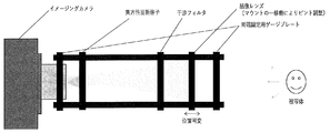
- It is a figure explaining the composition of the polarization imaging device used in the example.
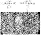
- It is an image of the result of an imaging measurement using the polarization imaging device which used scarlet beetle as a to-be-photographed object and was used in the Example. From the image obtained in FIG. 5, the images of the ⁇ 1st light component (I ⁇ 1 ) and the + 1st light component (I +1 ) are extracted by image processing, and the difference image is calculated to obtain the imaging image of S 3 Show.
- the present application provides a polarization imaging device comprising an anisotropic diffraction grating.
- "Polarization” which is a property in which the locus of the electric field vector of the electromagnetic wave describes a bias, is widely used as one of the characteristics of the electromagnetic wave.
- the polarization state of the electromagnetic wave changes, and the polarization change contains various information unique to the substance. That is, by measuring the polarization characteristic of the subject, it is possible to non-contact and nondestructively investigate information unique to the substance.
- the polarization imaging apparatus can perform imaging measurement of a spatial distribution of Stokes parameters (parameters describing the polarization state) of scattered light from an object by snapshot.
- the polarization imaging device of the present application has an anisotropic diffraction grating element, a lens element, and a light receiving element in which optical anisotropy is periodically modulated.
- the lens element, the anisotropic diffraction grating element, and the light receiving element may be arranged in order from the object side. Other elements other than those described above may be arranged as desired.
- the polarization imaging device of the present application has an anisotropic diffraction grating element whose optical anisotropy is periodically modulated.
- the principle of Stokes parameter measurement using the anisotropic diffraction grating element will be described below.
- the polarization state of the electromagnetic wave can be represented by a Stokes vector (S 0 , S 1 , S 2 , S 3 ) consisting of four elements.
- each Stokes parameter is defined by the following equation (1).
- the polarization characteristics of the subject can be clarified by finding these four elements from the intensity information of the light reflected, scattered and transmitted from the subject.
- the polarization imaging apparatus of the present application is characterized in that the imaging measurement of these Stokes parameters is performed at one time of image acquisition.
- the principle of polarization detection of this device is based on an anisotropic grating element whose optical anisotropy is modulated periodically.
- the Jones matrix representing the induced anisotropy distribution is represented by the following formula (2).
- ⁇ ⁇ nd / ⁇ , where ⁇ n is the maximum value of polarization induced birefringence, d is the film thickness of the recording material, and ⁇ is the wavelength of the diffracted light.
- Equation (3) the Jones matrix component contributing to the ⁇ 1st-order diffraction is represented by the following Equation (3).
- Equation (3) the intensity of the ⁇ 1-order diffracted light I PL ⁇ represented by the following formula (5) Is required. Therefore, it is understood that the diffracted light intensity of the anisotropic grating formed by PL recording strongly depends on the amplitude ratio angle ⁇ of the incident light.
- the lattice is referred to as a PL lattice unless otherwise specified in the present application.
- the diffracted light intensity of the anisotropic grating formed by the OC recording recorded by the OC interference depends on the phase difference of the incident light.
- the grid is referred to as an OC grid for the sake of simplicity.
- the anisotropic diffraction grating formed in the polarization recording material by polarization hologram recording exhibits diffraction characteristics depending on the incident polarization state. Therefore, polarization information of incident light can be spatially separated as intensity information. Therefore, the value of the Stokes parameter can be derived from the intensity information of each diffraction order light.
- the Stokes parameter detector with four anisotropic gratings with different grating vectors superimposed.
- FIG. 1 A schematic of the diffraction grating is shown in FIG.
- This anisotropic diffraction grating is one in which four gratings A, B, C, D are multiplexed and recorded in a polarization recording material.
- A, B, and C are PL lattices
- D is an OC lattice
- respective lattice vectors are arranged to form an angle of 45 degrees with each other.
- m A, B, C, D, and I A + means the intensity of + 1st order light with respect to the lattice A.
- I A ⁇ corresponding to PL grid, I B ⁇ , I C ⁇ is sinusoidally varies depending on ⁇ amplitude ratio angle of the incident light.
- the dependence of the incident polarized light on the amplitude ratio angle ⁇ of I A ⁇ , I B ⁇ and I C ⁇ is shown in FIG. 2 based on the diffraction characteristics of the PL grating. It can be seen from FIG. 2 that when I B > (I A + I C ) / 2, the amplitude ratio angle is ⁇ ⁇ 0, and when ⁇ (I A + I C ) / 2, the amplitude ratio angle is ⁇ > 0. That is, the sign of the amplitude ratio angle ⁇ ⁇ ⁇ can be obtained from the magnitude of I B.
- S 2 can be obtained by substituting the obtained amplitude ratio angle ⁇ and phase difference ⁇ into the above equation (1). Therefore, all elements of the Stokes parameter of the incident light can be determined from the diffracted lights I A , I B , I C and I D ⁇ from the anisotropic diffraction grating of FIG. In addition, if intensity information necessary for deriving a Stokes parameter can be obtained, measurement of the Stokes parameter is possible even with an anisotropic pattern different from the anisotropic diffraction grating of FIG.
- the anisotropic grating element may have an anisotropic grating having a plurality of grating vectors different in direction from one another, and at least the anisotropic orientation or the birefringence of the grating vector may be periodically modulated.
- the anisotropic diffraction grating element has an anisotropic diffraction grating that spatially separates information of the Stokes parameter of incident light according to the distribution of anisotropic orientation and birefringence, and converts it into intensity information. That's good.
- the anisotropic diffraction grating element has an anisotropic diffraction grating with good diffraction efficiency of ⁇ 1st-order light.
- an anisotropic grating element can be prepared as follows. That is, the anisotropic diffraction grating element has a photoreactive side chain having at least one kind of reaction selected from the group consisting of (A-1) photocrosslinking and (A-2) photoisomerization. It may include an anisotropic diffraction grating having a polymer film. In addition, the anisotropic diffraction grating element preferably includes an anisotropic diffraction grating made of a photoreactive polymer film.
- the photoreactive polymer used for the photoreactive polymer film is desired Polymers capable of inducing a large retardation, specifically the retardation in the above-mentioned range, by the interference exposure of polarized light are preferable.
- An anisotropic grating element is And I) a first transparent substrate layer; and II) a first photoreactive side chain which causes at least one reaction selected from the group consisting of (A-1) photocrosslinking, and (A-2) photoisomerization.
- it includes an anisotropic diffraction grating having a first photoreactive polymer film.
- anisotropic diffraction grating elements And III) a second transparent substrate layer; and IV) a second photoreactive side chain which causes at least one reaction selected from the group consisting of (A-1) photocrosslinking, and (A-2) photoisomerization.
- a second photoreactive polymer film having The II) first photoreactive polymer film and the IV) second photoreactive polymer film are disposed to face each other, and the II) first film and the IV) second film In between, it is preferable to include an anisotropic diffraction grating in which the low molecular weight liquid crystal layer is disposed.
- First and second transparent substrate layers are made of a transparent substrate.
- a transparent substrate although it depends on the characteristics used as a polarization imaging device, for example, glass; plastics such as acrylic and polycarbonate; and the like can be used.
- a transparent substrate it is preferable to have the property of transmitting polarized ultraviolet light.
- (B) Low Molecular Weight Liquid Crystal Layer nematic liquid crystals, ferroelectric liquid crystals, etc. which are conventionally used in liquid crystal display elements and the like can be used.
- cyanobiphenyls such as 4-cyano-4'-n-pentylbiphenyl and 4-cyano-4'-n-feptyloxybiphenyl as low-molecular liquid crystals
- cholesteryl esters such as cholesteryl acetate and cholesteryl benzoate Carbonates such as 4-carboxyphenylethyl carbonate, 4-carboxyphenyl-n-butyl carbonate
- phenyl esters such as phenyl benzoate and biphenyl phthalate
- benzylidene-2-naphthylamine 4'- Schiff bases such as n-butoxybenzylidene-4-acetylaniline
- benzidines such as N, N'-bisbenzylidene benzidine, p-dianisalbenzidine
- 4,4'-azoxydianisole, 4,4'- Azox such as di-n-butoxy azoxybenzene Benzene; specifically shown phen
- interference exposure of desired polarized light is performed on the above-mentioned photoreactive polymer film, and an arbitrary diffraction pattern is formed on the polymer thin film to obtain information on the Stokes parameters of light incident on the polymer thin film, It is preferable to use an anisotropic diffraction grating that is spatially separated according to the distribution of anisotropic orientation and birefringence formed in the polymer thin film, and converted to intensity information.
- the photoreactive polymer film described above has a photoreactive side chain which causes at least one reaction selected from the group consisting of (A-1) photocrosslinking and (A-2) photoisomerization. It should be formed with a macromolecule.
- photoreactive refers to the property of producing (A-1) photocrosslinking or (A-2) photoisomerization reaction; and both reactions.
- the photoreactive polymer preferably has a side chain which causes (A-1) photocrosslinking reaction.
- the photoreactive polymer is i) a polymer that exhibits liquid crystallinity in a predetermined temperature range, and is a polymer having a photoreactive side chain.
- the photoreactive polymer should be ii) reactive with light in the wavelength range of 250 nm to 450 nm and exhibit liquid crystallinity in the temperature range of 50 to 300 ° C.
- the photoreactive polymer preferably has a photoreactive side chain that responds to light in the wavelength range of 250 nm to 450 nm, particularly polarized ultraviolet light.
- the photoreactive polymer preferably has a mesogenic group to exhibit liquid crystallinity in a temperature range of 50 to 300 ° C.
- the photoreactive polymer has a photoreactive side chain having photoreactivity.
- the structure of the side chain is not particularly limited, it has a structure that produces the reaction shown in the above (A-1) and / or (A-2), and has a structure that produces the (A-1) photocrosslinking reaction Is preferred.
- the structure causing the photocrosslinking reaction is preferable in that the structure after the reaction can stably maintain the orientation of the photoreactive polymer for a long time even if it is exposed to external stress such as heat. .
- the structure of the side chain of the photoreactive polymer is preferably one having a rigid mesogenic component because the alignment of the liquid crystal is stabilized.
- mesogen component examples include, but are not limited to, biphenyl group, terphenyl group, phenylcyclohexyl group, phenylbenzoate group, azobenzene group and the like.
- the main chain of the photoreactive polymer for example, radically polymerizable groups such as hydrocarbon, (meth) acrylate, itaconate, fumarate, maleate, ⁇ -methylene- ⁇ -butyrolactone, styrene, vinyl, maleimide, norbornene and the like Although there can be mentioned at least one selected from the group consisting of siloxanes, it is not limited thereto.
- the side chain of the photoreactive polymer is preferably a side chain comprising at least one of the following formulas (1) to (6).
- S is an alkylene group having 1 to 12 carbon atoms, and a hydrogen atom bonded to them may be replaced by a halogen group
- T is a single bond or an alkylene group having 1 to 12 carbon atoms, and a hydrogen atom bonded to them may be replaced by a halogen group
- Y 1 represents a ring selected from monovalent benzene ring, naphthalene ring, biphenyl ring, furan ring, pyrrole ring and alicyclic hydrocarbon having 5 to 8 carbon atoms, or the same or selected from their substituents
- 2 to 6 different rings are bonded to each other via a bonding group B, and hydrogen atoms
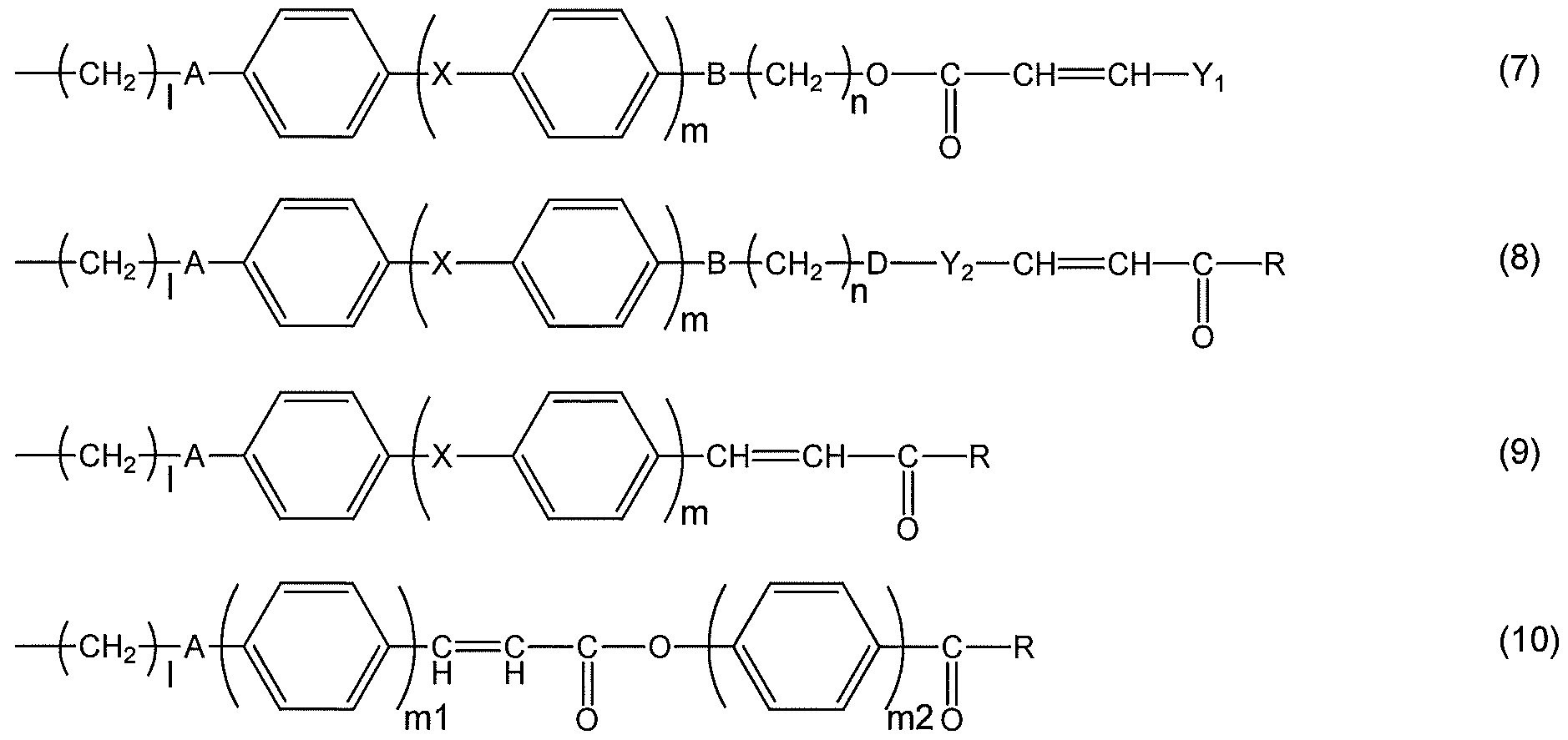
- the side chain is preferably any one type of photoreactive side chain selected from the group consisting of the following formulas (7) to (10).
- A, B, D, Y 1 , X, Y 2 and R have the same definition as above; l represents an integer of 1 to 12; m represents an integer of 0 to 2; m1 and m2 represent an integer of 1 to 3; n represents an integer of 0 to 12 (provided that n is 0 and B is a single bond).
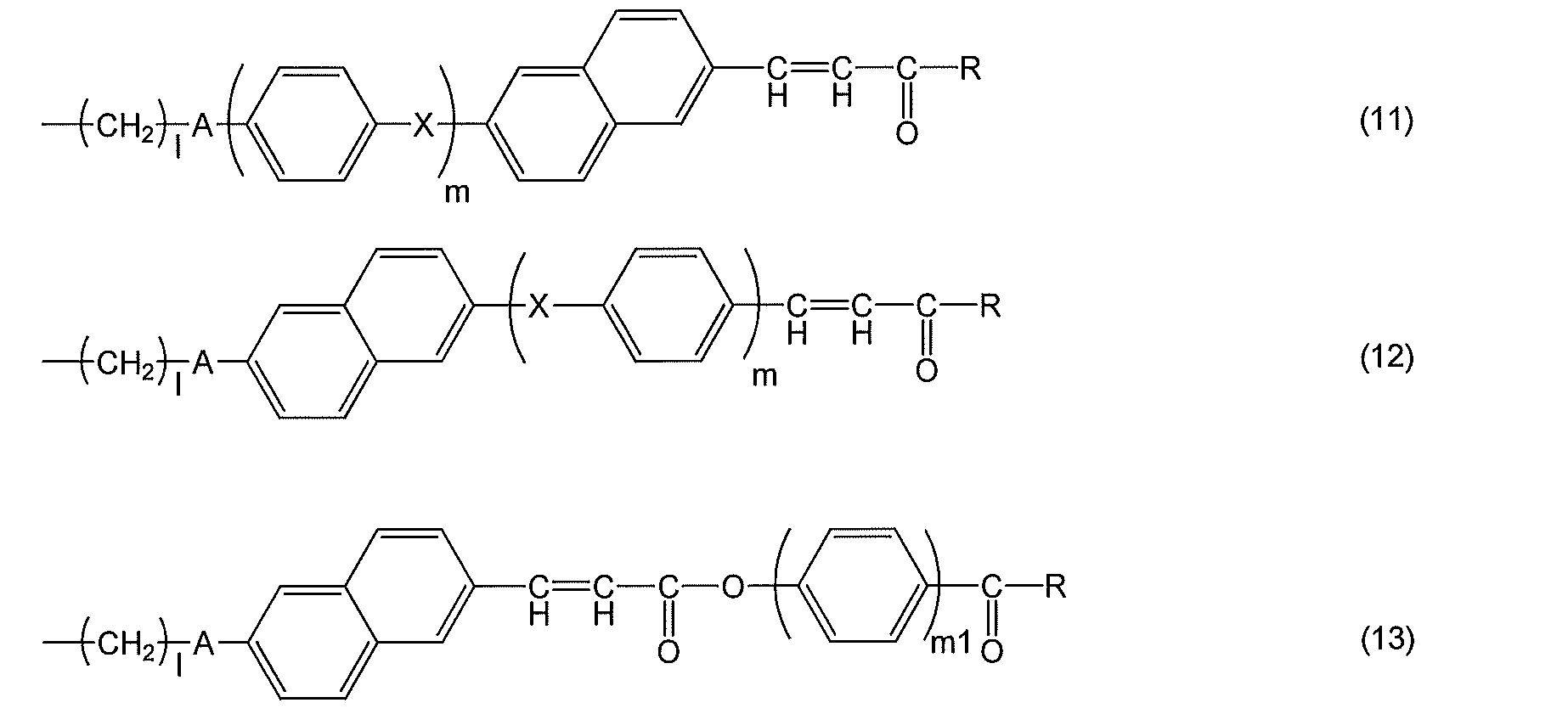
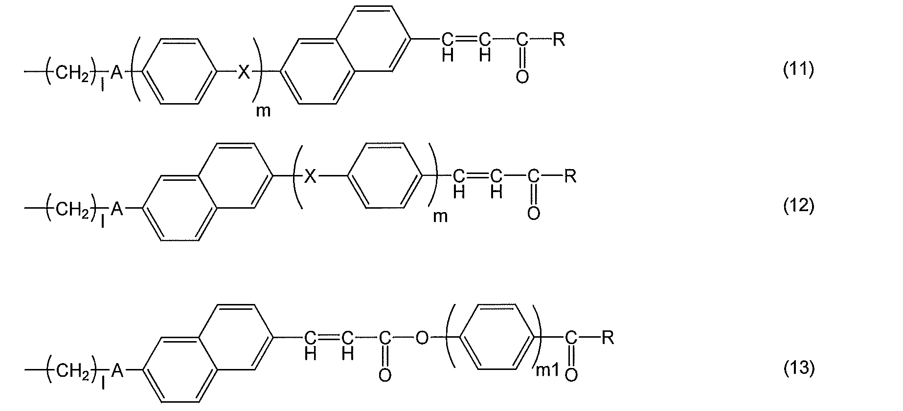
- the side chain is preferably any one type of photoreactive side chain selected from the group consisting of the following formulas (11) to (13).
- A, X, l, m, m1 and R have the same definition as above.
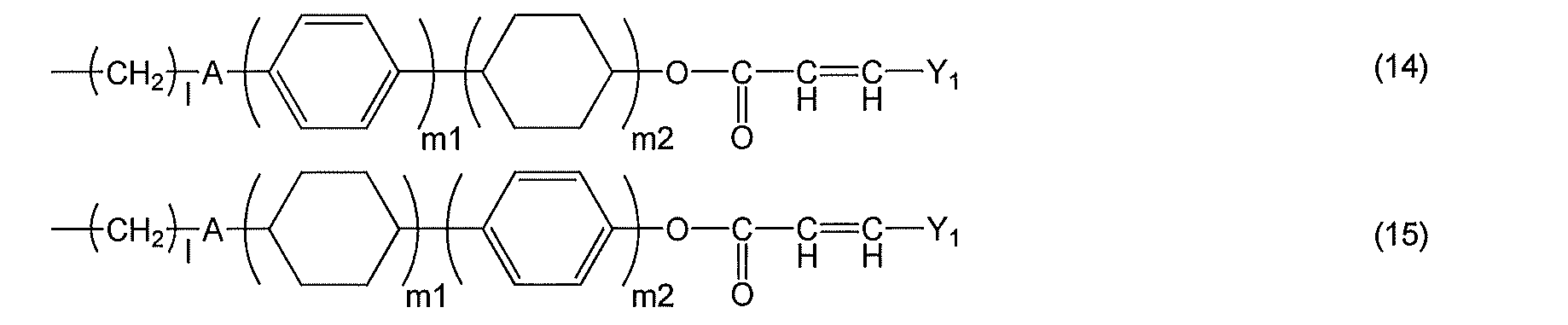
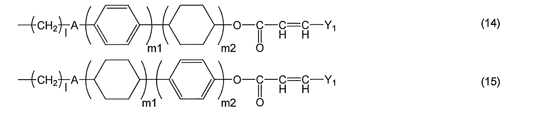
- the side chain is preferably a photoreactive side chain represented by the following formula (14) or (15). Wherein A, Y 1 , l, m 1 and m 2 have the same definition as above.
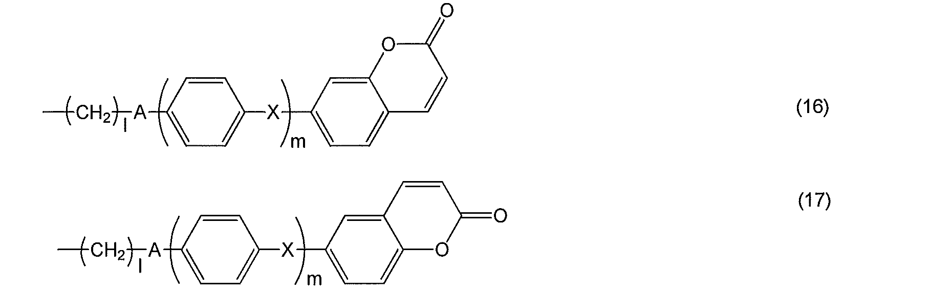
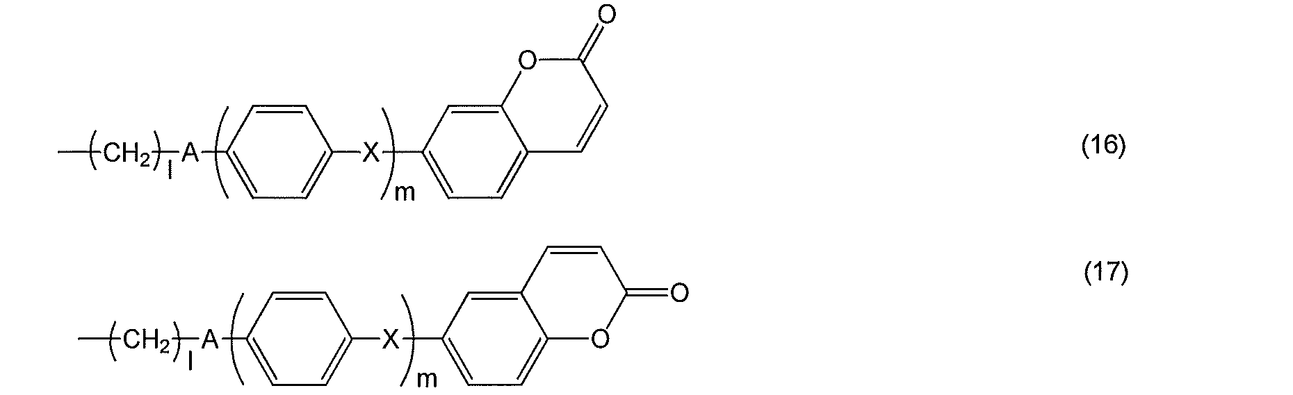
- the side chain is preferably a photoreactive side chain represented by the following formula (16) or (17).
- A, X, l and m have the same definition as above.
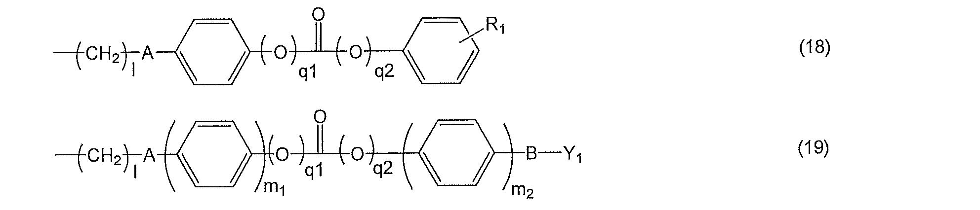
- the side chain may be a photoreactive side chain represented by the following formula (18) or (19). (Wherein, A, B, Y 1 and R 1 have the same definition as described above. One of q1 and q2 is 1 and the other is 0; l represents an integer of 1 to 12, m1 and m2 represent an integer of 1 to 3;
- the side chain is preferably a photoreactive side chain represented by the following formula (20). Wherein A, Y 1 , X, l and m have the same definition as above.
- a polymer having any one type of liquid crystalline side chain selected from the group consisting of the following formulas (21) to (31) may be included.
- the photoreactive side chain of the above-mentioned polymer forming the photoreactive polymer film does not have liquid crystallinity, or the above-mentioned polymer main chain forming the photoreactive polymer film is liquid crystalline If not, the component forming the photoreactive polymer film may have any one type of liquid crystalline side chain selected from the group consisting of the following formulas (21) to (31).
- Y 3 is a group selected from the group consisting of monovalent benzene ring, naphthalene ring, biphenyl ring, furan ring, nitrogen-containing heterocycle, alicyclic hydrocarbon having 5 to 8 carbon atoms, and a combination thereof
- the hydrogen atoms bonded to them may be each independently substituted with -NO 2 , -CN, a halogen group, an alkyl group of 1 to 5 carbon atoms, or an alkyloxy group of 1 to 5 carbon atoms
- the above-mentioned photoreactive polymer film is obtained by polymerizing a photoreactive side chain monomer having the above-mentioned photoreactive side chain, and in some cases, the photoreactive side chain monomer and the monomer having the above-mentioned liquid crystalline side chain Can be obtained by copolymerizing For example, it can be manufactured by referring to [0062] to [0090] of WO 2017/061536 (the contents of the publication are all incorporated herein by reference).
- the polarization imaging device of the present invention has a lens element.
- the lens element is not particularly limited as long as it has an effect of forming an image in a light receiving element described later.
- the polarization imaging device of the present invention has a light receiving element.
- the light receiving element is not particularly limited as long as the above-mentioned S 0 to S 3 can be obtained from the image data.
- FIG. 3 is a view for explaining the outline of the polarization imaging apparatus of the present invention.
- the polarization imaging apparatus of the present invention comprises an imaging lens, a color filter, an anisotropic diffraction grating, and a light receiving element array.
- the imaging lens has a variable arrangement distance from the light receiving element array so that focus adjustment can be performed.
- the diffraction angle of the anisotropic diffraction grating has wavelength dependency, so that for white light, angular dispersion may cause a problem of blurring of the image. Therefore, color filters are inserted to reduce the influence of dispersion.
- the anisotropic diffraction grating is used in combination with an interference filter of a corresponding frequency band in which retardation is optimized according to the observation wavelength.
- the imaging unit imaging lens, light receiving element array
- the imaging unit imaging lens, light receiving element array
- the light intensity of 0 deg linear polarization component, 90 deg linear polarization component, 45 deg linear polarization component, -45 deg linear polarization component, right-handed circularly polarized light component, left-handed circularly polarized light component shown in equation (1) can be calculated generally
- a method of measuring is used, or a Fourier analysis method such as a rotational retarder method is used.
- these methods are not suitable for the measurement of an object whose state changes with time, because in principle multiple measurements are required.
- polarization imaging measurement in snapshot can be performed by spatially separating information necessary for measurement of Stokes parameters and acquiring the information at a time as intensity information. That is, it is characterized in that it can measure even a dynamic object to be measured. In addition, it is one of the features that it is inexpensive because it does not require an expensive optical element including a diffraction grating.
- the polarization imaging value of the present invention can be measured two-dimensionally regardless of whether it is a dynamic measurement target or a static measurement target, so that it can be applied to various fields. Examples include, but are not limited to, the medical field, the field of autonomous driving technology of automobiles, the field of security, and the like.
- the present invention will be specifically described using examples, but the present invention is not limited only by the examples.
- P6CB photocrosslinkable polymer liquid crystal (4- (4-methoxycinnamoyloxy) biphenyl side groups (P6CB)) represented by the following formula was used.
- P6CB was dissolved in dichloromethane, and spin-coated on a glass substrate to a film thickness of 300 nm. Two glass substrates coated with the P6CB film were prepared, and the P6CB film side was made to face each other to bond them, and an empty cell was created.
- the produced empty cell was irradiated with an exposure energy of 600 mJ / cm 2 while causing OC interference of an ultraviolet laser having a wavelength of 325 nm emitted from a He-Cd laser. After irradiation, heat treatment was performed in an oven at 150 ° C. for 15 minutes, and after heat treatment, low molecular liquid crystal 5CB (4-cyano-4′-pentylbiphenyl) was injected into the cell to prepare a cell type OC lattice. The diameter of the produced anisotropic diffraction grating was 8 mm.
- the polarization imaging apparatus includes, in order from the object, an imaging lens, an interference filter (FL532-3 manufactured by Throrlabs (central wavelength 532 nm), the anisotropic diffraction grating obtained above, A commercially available camera (ILCE6000S manufactured by SONY) is used as the light receiving element, and the imaging lens, interference filter, and anisotropic diffraction grating are packaged in a gauge system, and the commercially available camera is used. Designed to be worn.
- Imaging measurement was performed using a beetle that exhibits selective reflection characteristics for circularly polarized light as a subject.
- the image is shown in FIG. It can be seen from FIG. 5 that three image spots are obtained. From left to right, it corresponds to ⁇ 1st order light, 0th order light and + 1st order light component of the OC grating.
- the ⁇ 1st order light component and the + 1st order light component represent a two-dimensional distribution of the left-handed circularly polarized light component and the right-handed circularly polarized light component.
- the image of the -1st-order light component (I -1) and + 1st-order light component (I + 1) extracted by image processing Figure 6 shows the imaging image of S 3 obtained by performing the difference calculation based on the following formula .
Landscapes
- Physics & Mathematics (AREA)
- General Physics & Mathematics (AREA)
- Spectroscopy & Molecular Physics (AREA)
- Optics & Photonics (AREA)
- Chemical & Material Sciences (AREA)
- Polymers & Plastics (AREA)
- Chemical Kinetics & Catalysis (AREA)
- Medicinal Chemistry (AREA)
- Health & Medical Sciences (AREA)
- Organic Chemistry (AREA)
- Addition Polymer Or Copolymer, Post-Treatments, Or Chemical Modifications (AREA)
- Compositions Of Macromolecular Compounds (AREA)
- Diffracting Gratings Or Hologram Optical Elements (AREA)
- Spectrometry And Color Measurement (AREA)
- Blocking Light For Cameras (AREA)
- Polarising Elements (AREA)
- Eye Examination Apparatus (AREA)
- Closed-Circuit Television Systems (AREA)
- Cage And Drive Apparatuses For Elevators (AREA)
Abstract
Description
最も代表的な偏光計測の手法は、回転する偏光子及び波長板を利用する回転検光子法と回転移相子法である。これらの手法では、偏光素子を回転させながら入射光の偏光状態に応じた光強度の時間波形を観測する。さらに得られた時間波形をフーリエ解析し、ストークスパラメータの情報を復元する。この手法は研究の歴史が長く、様々な誤差低減が施されており測定精度が高いことが特徴である。しかし一方で、時間的に偏光素子を回転させながら複数回に分けてストークスパラメータの復元に必要な情報を取得するため、時間的に偏光状態が変化するような被測定物には不向きな手法である。偏光計測を医療装置やリモートセンシング等へと応用することを考えると、動的な物体の偏光状態の測定の必要性は極めて高く、スナップショットでの偏光空間分布計測が求められる。
その一例は、光受光素子アレイ上に波長板ないし偏光子をその光学軸方位を4方位に分けたものを分布させ、4画素あたりで回転検光子法ないし回転移相子法に相当する計測を担わせるというものである(非特許文献1又は2)。本手法では、偏光素子を回転させるための機械的稼動部が不要であり、さらに一度の画像取得でストークスパラメータの取得に必要な情報が得られるので、静的且つスナップショットでのイメージング偏光計測が可能となる。しかしながら、光受光素子のアレイと偏光素子のアレイの位置を正確に合わせる必要があり、作製が容易ではない。また、偏光素子アレイの境界部で生じる位相差の不連続性により、測定上好ましくない回折光が生じるおそれもある。
この手法では前述のアレイ素子のような回折の影響が生じない。ただし、本手法ではサバール板等の高額な光学素子を要するため、コストが大きくかかる難点がある。
<1> 光学異方性が周期的に変調された異方性回折格子素子、レンズ素子、及び受光素子を有する偏光撮像装置。
<2> 上記<1>において、異方性回折格子素子が、互いに方向の異なる複数個の格子ベクトルを有する異方性回折格子を有し、前記格子ベクトルは少なくとも異方性方位又は複屈折が周期的に変調されるのがよい。
<3> 上記<1>又は<2>において、異方性回折格子素子が、入射光のストークスパラメータの情報を、異方性方位および複屈折の分布に応じて空間的に分離し、強度情報へと変換する異方性回折格子を有するのがよい。
<5> 上記<1>~<4>のいずれかにおいて、異方性回折格子素子が、光反応性高分子膜からなる異方性回折格子を含むのがよい。
<6> 上記<1>~<5>のいずれかにおいて、異方性回折格子素子が、
I)第1の透明基体層;及び
II)(A-1)光架橋、及び(A-2)光異性化からなる群から選ばれる少なくとも1種の反応を生じる第1の光反応性側鎖を有する第1の光反応性高分子膜
を有する異方性回折格子を含むのがよい。
III)第2の透明基体層;及び
IV)(A-1)光架橋、及び(A-2)光異性化からなる群から選ばれる少なくとも1種の反応を生じる第2の光反応性側鎖を有する第2の光反応性高分子膜;及び
を有し、
前記II)第1の光反応性高分子膜と前記IV)第2の光反応性高分子膜とが対向するように配置し、前記II)第1の膜及び前記IV)第2の膜の間に、(B)低分子液晶層が配置される異方性回折格子を含むのがよい。
<9> 上記<1>~<8>のいずれかにおいて、異方性回折格子素子が±1次光の回折効率が良い異方性回折格子を有するのがよい。
(式中、A、B、Dはそれぞれ独立に、単結合、-O-、-CH2-、-COO-、-OCO-、-CONH-、-NH-CO-、-CH=CH-CO-O-、又は-O-CO-CH=CH-を表す;
Sは、炭素数1~12のアルキレン基であり、それらに結合する水素原子はハロゲン基に置き換えられていてもよい;
Tは、単結合または炭素数1~12のアルキレン基であり、それらに結合する水素原子はハロゲン基に置き換えられていてもよい;
Y1は、1価のベンゼン環、ナフタレン環、ビフェニル環、フラン環、ピロール環および炭素数5~8の脂環式炭化水素から選ばれる環を表すか、それらの置換基から選ばれる同一又は相異なった2~6の環が結合基Bを介して結合してなる基であり、それらに結合する水素原子はそれぞれ独立に-COOR0(式中、R0は水素原子又は炭素数1~5のアルキル基を表す)、-NO2、-CN、-CH=C(CN)2、-CH=CH-CN、ハロゲン基、炭素数1~5のアルキル基、又は炭素数1~5のアルキルオキシ基で置換されても良い;
Y2は、2価のベンゼン環、ナフタレン環、ビフェニル環、フラン環、ピロール環、炭素数5~8の脂環式炭化水素、および、それらの組み合わせからなる群から選ばれる基であり、それらに結合する水素原子はそれぞれ独立に-NO2、-CN、-CH=C(CN)2、-CH=CH-CN、ハロゲン基、炭素数1~5のアルキル基、又は炭素数1~5のアルキルオキシ基で置換されても良い;
Rは、ヒドロキシ基、炭素数1~6のアルコキシ基を表すか、又はY1と同じ定義を表す;
Xは、単結合、-COO-、-OCO-、-N=N-、-CH=CH-、-C≡C-、-CH=CH-CO-O-、又は-O-CO-CH=CH-を表し、Xの数が2となるときは、X同士は同一でも異なっていてもよい;
Couは、クマリン-6-イル基またはクマリン-7-イル基を表し、それらに結合する水素原子はそれぞれ独立に-NO2、-CN、-CH=C(CN)2、-CH=CH-CN、ハロゲン基、炭素数1~5のアルキル基、又は炭素数1~5のアルキルオキシ基で置換されても良い;
q1とq2は、一方が1で他方が0である;
q3は0または1である;
P及びQは、各々独立に、2価のベンゼン環、ナフタレン環、ビフェニル環、フラン環、ピロール環、炭素数5~8の脂環式炭化水素、および、それらの組み合わせからなる群から選ばれる基である;ただし、Xが-CH=CH-CO-O-、-O-CO-CH=CH-である場合、-CH=CH-が結合する側のP又はQは芳香環であり、Pの数が2以上となるときは、P同士は同一でも異なっていてもよく、Qの数が2以上となるときは、Q同士は同一でも異なっていてもよい;
l1は0または1である;
l2は0~2の整数である;
l1とl2がともに0であるときは、Tが単結合であるときはAも単結合を表す;
l1が1であるときは、Tが単結合であるときはBも単結合を表す;
H及びIは、各々独立に、2価のベンゼン環、ナフタレン環、ビフェニル環、フラン環、ピロール環、およびそれらの組み合わせから選ばれる基である。)
からなる群から選ばれるいずれか1種の光反応性側鎖を有する光反応性高分子を有するのがよい。

(式中、A、B、Dはそれぞれ独立に、単結合、-O-、-CH2-、-COO-、-OCO-、-CONH-、-NH-CO-、-CH=CH-CO-O-、又は-O-CO-CH=CH-を表す;
Y1は、1価のベンゼン環、ナフタレン環、ビフェニル環、フラン環、ピロール環および炭素数5~8の脂環式炭化水素から選ばれる環を表すか、それらの置換基から選ばれる同一又は相異なった2~6の環が結合基Bを介して結合してなる基であり、それらに結合する水素原子はそれぞれ独立に-COOR0(式中、R0は水素原子又は炭素数1~5のアルキル基を表す)、-NO2、-CN、-CH=C(CN)2、-CH=CH-CN、ハロゲン基、炭素数1~5のアルキル基、又は炭素数1~5のアルキルオキシ基で置換されても良い;
Xは、単結合、-COO-、-OCO-、-N=N-、-CH=CH-、-C≡C-、-CH=CH-CO-O-、又は-O-CO-CH=CH-を表し、Xの数が2となるときは、X同士は同一でも異なっていてもよい;
lは1~12の整数を表す;
mは、0~2の整数を表し、m1、m2は1~3の整数を表す;
nは0~12の整数(ただしn=0のときBは単結合である)を表す;
Y2は、2価のベンゼン環、ナフタレン環、ビフェニル環、フラン環、ピロール環、炭素数5~8の脂環式炭化水素、および、それらの組み合わせからなる群から選ばれる基であり、それらに結合する水素原子はそれぞれ独立に-NO2、-CN、-CH=C(CN)2、-CH=CH-CN、ハロゲン基、炭素数1~5のアルキル基、又は炭素数1~5のアルキルオキシ基で置換されても良い;
Rは、ヒドロキシ基、炭素数1~6のアルコキシ基を表すか、又はY1と同じ定義を表す)
からなる群から選ばれるいずれか1種の光反応性側鎖を有する光反応性高分子を有するのがよい。
(式中、Aは、それぞれ独立に、単結合、-O-、-CH2-、-COO-、-OCO-、-CONH-、-NH-CO-、-CH=CH-CO-O-、又は-O-CO-CH=CH-を表す;
Xは、単結合、-COO-、-OCO-、-N=N-、-CH=CH-、-C≡C-、-CH=CH-CO-O-、又は-O-CO-CH=CH-を表し、Xの数が2となるときは、X同士は同一でも異なっていてもよい;
lは、1~12の整数を表し、mは0~2の整数を表し、m1は1~3の整数を表す;
Rは、1価のベンゼン環、ナフタレン環、ビフェニル環、フラン環、ピロール環および炭素数5~8の脂環式炭化水素から選ばれる環を表すか、それらの置換基から選ばれる同一又は相異なった2~6の環が結合基Bを介して結合してなる基であり、それらに結合する水素原子はそれぞれ独立に-COOR0(式中、R0は水素原子又は炭素数1~5のアルキル基を表す)、-NO2、-CN、-CH=C(CN)2、-CH=CH-CN、ハロゲン基、炭素数1~5のアルキル基、又は炭素数1~5のアルキルオキシ基で置換されても良いか、又はヒドロキシ基もしくは炭素数1~6のアルコキシ基を表す)
からなる群から選ばれるいずれか1種の光反応性側鎖を有する光反応性高分子を有するのがよい。

(式中、Aはそれぞれ独立に、単結合、-O-、-CH2-、-COO-、-OCO-、-CONH-、-NH-CO-、-CH=CH-CO-O-、又は-O-CO-CH=CH-を表す;
Y1は、1価のベンゼン環、ナフタレン環、ビフェニル環、フラン環、ピロール環および炭素数5~8の脂環式炭化水素から選ばれる環を表すか、それらの置換基から選ばれる同一又は相異なった2~6の環が結合基Bを介して結合してなる基であり、それらに結合する水素原子はそれぞれ独立に-COOR0(式中、R0は水素原子又は炭素数1~5のアルキル基を表す)、-NO2、-CN、-CH=C(CN)2、-CH=CH-CN、ハロゲン基、炭素数1~5のアルキル基、又は炭素数1~5のアルキルオキシ基で置換されても良い;
lは1~12の整数を表し、m1、m2は1~3の整数を表す)
で表される光反応性側鎖を有する光反応性高分子を有するのがよい。
Xは、単結合、-COO-、-OCO-、-N=N-、-CH=CH-、-C≡C-、-CH=CH-CO-O-、又は-O-CO-CH=CH-を表し、Xの数が2となるときは、X同士は同一でも異なっていてもよい;
lは、1~12の整数を表し、mは0~2の整数を表す)
で表される光反応性側鎖を有する光反応性高分子を有するのがよい。
(式中、A、Bはそれぞれ独立に、単結合、-O-、-CH2-、-COO-、-OCO-、-CONH-、-NH-CO-、-CH=CH-CO-O-、又は-O-CO-CH=CH-を表す;
Y1は、1価のベンゼン環、ナフタレン環、ビフェニル環、フラン環、ピロール環および炭素数5~8の脂環式炭化水素から選ばれる環を表すか、それらの置換基から選ばれる同一又は相異なった2~6の環が結合基Bを介して結合してなる基であり、それらに結合する水素原子はそれぞれ独立に-COOR0(式中、R0は水素原子又は炭素数1~5のアルキル基を表す)、-NO2、-CN、-CH=C(CN)2、-CH=CH-CN、ハロゲン基、炭素数1~5のアルキル基、又は炭素数1~5のアルキルオキシ基で置換されても良い;
q1とq2は、一方が1で他方が0である;
lは1~12の整数を表し、m1、m2は1~3の整数を表す;
R1は、水素原子、-NO2、-CN、-CH=C(CN)2、-CH=CH-CN、ハロゲン基、炭素数1~5のアルキル基、又は炭素数1~5のアルキルオキシ基を表す)
からなる群から選ばれるいずれか1種の感光性側鎖を有する光反応性高分子を有するのがよい。

(式中、Aは、単結合、-O-、-CH2-、-COO-、-OCO-、-CONH-、-NH-CO-、-CH=CH-CO-O-、又は-O-CO-CH=CH-を表す;
Y1は、1価のベンゼン環、ナフタレン環、ビフェニル環、フラン環、ピロール環および炭素数5~8の脂環式炭化水素から選ばれる環を表すか、それらの置換基から選ばれる同一又は相異なった2~6の環が結合基Bを介して結合してなる基であり、それらに結合する水素原子はそれぞれ独立に-COOR0(式中、R0は水素原子又は炭素数1~5のアルキル基を表す)、-NO2、-CN、-CH=C(CN)2、-CH=CH-CN、ハロゲン基、炭素数1~5のアルキル基、又は炭素数1~5のアルキルオキシ基で置換されても良い;
Xは、単結合、-COO-、-OCO-、-N=N-、-CH=CH-、-C≡C-、-CH=CH-CO-O-、又は-O-CO-CH=CH-を表し、Xの数が2となるときは、X同士は同一でも異なっていてもよい;
lは1~12の整数を表し、mは0~2の整数を表す)で表される光反応性側鎖を有する光反応性高分子を有するのがよい。

本願は、異方性回折格子を具備する偏光撮像装置を提供する。
電磁波の電場ベクトルの軌跡が偏りを描く性質である「偏光」は、電磁波の持つ一つの特性として幅広く利用されている。電磁波が物質と相互作用(反射・散乱・吸収など)すると、電磁波の偏光状態が変わり、その偏光変化には物質固有の様々な情報が含まれている。すなわち、被写体の偏光特性を測定することで、物質固有の情報を非接触・非破壊で調べることができる。本願の偏光撮像装置は、被写体からの散乱光のストークスパラメータ(偏光状態を記述するパラメータ)の空間分布をスナップショットでイメージング計測を行うことができる。
なお、被写体側から順に、レンズ素子、異方性回折格子素子、及び受光素子を配置するのがよい。上述の素子以外の、その他の素子を所望により配置してもよい。
本願の偏光撮像装置は、光学異方性が周期的に変調された異方性回折格子素子を有する。該異方性回折格子素子を用いたストークスパラメータ測定の原理を以下に説明する。
電磁波の偏光状態は4つの要素から成るストークスベクトル(S0,S1,S2,S3)で表すことができる。
ここで、S0:全光強度、S1:0deg直線偏光成分と90deg直線偏光成分の差、S2:45deg直線偏光成分と-45deg直線偏光成分の差、S3:右回り円偏光成分と左回り円偏光成分の差を意味しており、ストークスパラメータと呼ばれる。
0deg直線偏光成分と90deg直線偏光成分の間の振幅比角と位相差をそれぞれΨとΔとすると、各ストークスパラメータは下記式(1)で定義される。

本願の偏光撮像装置は、これらストークスパラメータを1度の画像取得でイメージング計測することを特徴とする。本装置の偏光検出の原理は、光学異方性が周期的に変調された異方性回折格子素子に基づく。
装置の構成等について述べる前に、偏光ホログラム記録により作製される異方性回折格子の回折特性について述べる。

したがって、PL記録により形成された異方性格子の回折光強度は、入射光の振幅比角Ψに強く依存することが分かる。以降、本願において特記しない限り、該格子をPL格子と称する。

また、式(6)を展開して下記式(7)を得ることができ、式(7)から、PL記録の場合と同様に、式(4)で与えられる入射偏光に対する回折光の強度を求めると、下記式(8)で表すTOC ±が求められる。
したがって、OC干渉により記録されたOC記録により形成された異方性格子の回折光強度は、入射光の位相差に依存することが分かる。以降、簡単のために本格子をOC格子と称する。

この異方性回折格子は、4つの格子A,B,C,Dを偏光記録材料内で多重記録したものである。このうち、A,B,CはPL格子、DはOC格子であり、それぞれの格子ベクトルは互いに45度の角度を成すように配置されている。ここで、各格子は記録材料中で独立に形成されているものと仮定し、この膜に偏光した光を垂直入射させた場合にスクリーン上で観測される±1次の回折光の強度をIm+およびIm-と定義する。なお、m=A, B, C, Dであり、IA+は格子Aに対する+1次光の強度を意味する。
ここで、上記式(5)から分かるように、PL格子に対応するIA±,IB±,IC±は入射光の振幅比角Ψに依存して正弦的に変化する。また、m式(5)からPL格子の場合は入射光の偏光状態に依存せずに±1次の回折光強度が等しくなるので、IA+=IA-=IA、IB+=IB-=IB、IC+=IC-=ICが成り立つ。
一方、式(8)より、OC格子に対応するID±は入射光の位相差Δに依存して振動する。
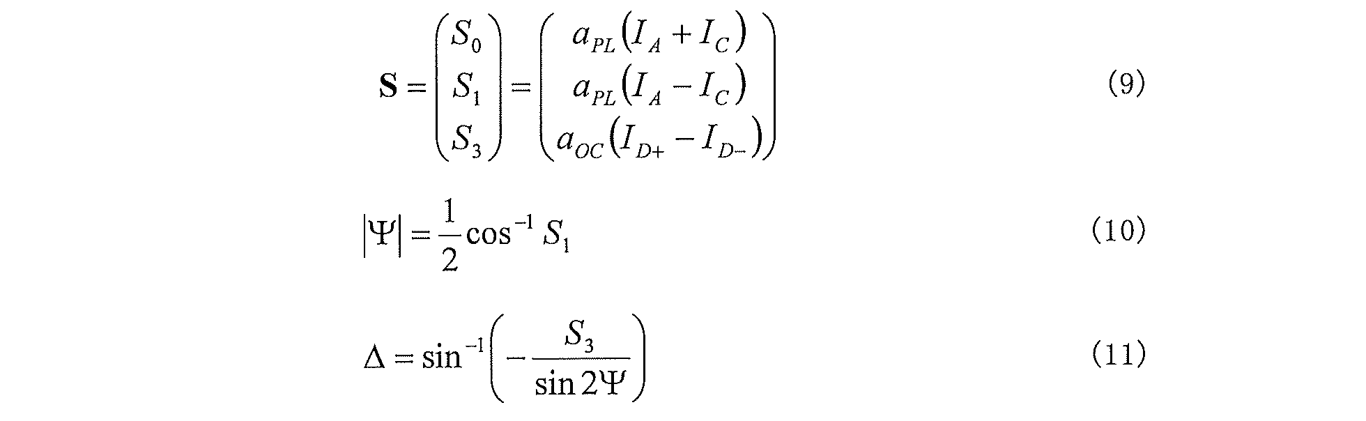
以上より、ストークスパラメータの内S0、S1、S3は式(1)から、下記式(9)が求められる。ここで、aPLとaOCは比例定数である。
一方、式(1)から下記式(10)及び(11)が求められる。
ここで、PL格子の回折特性に基づいてIA±,IB±,IC±の入射偏光の振幅比角Ψに対する依存性を図2に示す。
図2から、IB>(IA+IC)/2のとき振幅比角はΨ<0となり、<(IA+IC)/2のとき振幅比角はΨ>0となることがわかる。
即ち、IBの大きさから振幅比角Ψの符号を求めることができる。さらに、得られた振幅比角Ψと位相差Δを上記式(1)に代入することによりS2が求められる。したがって、図1の異方性回折格子からの回折光IA,IB,IC,ID±から入射光のストークスパラメータの全要素を求めることができる。なお、ストークスパラメータの導出に必要な強度情報が得られるのであれば、図1の異方性回折格子とは異なる異方性パターンでもストークスパラメータの測定は可能である。
また、異方性回折格子素子が、入射光のストークスパラメータの情報を、異方性方位および複屈折の分布に応じて空間的に分離し、強度情報へと変換する異方性回折格子を有するのがよい。さらに、異方性回折格子素子が±1次光の回折効率が良い異方性回折格子を有するのがよい。PL格子、OC格子それぞれにおいて、±1次光の回折効率が最も良い理想的な位相差は上記式(5)と(8)から求められる。
具体的には、OC格子の場合、5%以上の回折効率、即ち位相差(δ=2πΔnd/λ)では0.448+2πm~5.82+2πm(m:自然数)の範囲、好ましくは50%以上の回折効率、即ち位相差(δ=2πΔnd/λ)では1.57+2πm~4.71+2πm(m:自然数)の範囲、理想的には100%の回折効率、即ち位相差(δ=2πΔnd/λ)では3.14+2πm(m:自然数)であるのがよい。
また、PL格子の場合、5%以上の回折効率、即ち位相差(δ=2πΔnd/λ)では0.916~6.58、9.70~12.4、15.8~18.3、22.8~24.0の範囲、好ましくは15%以上の回折効率、即ち位相差(δ=2πΔnd/λ)では1.69~5.72の範囲、理想的には33.8%の回折効率、即ち位相差(δ=2πΔnd/λ)では3.68であるのがよい。
即ち、異方性回折格子素子は、(A-1)光架橋、及び(A-2)光異性化からなる群から選ばれる少なくとも1種の反応を生じる光反応性側鎖を有する光反応性高分子膜を有する異方性回折格子を含むのがよい。
また、異方性回折格子素子が、光反応性高分子膜からなる異方性回折格子を含むのがよい。この場合、光反応性高分子膜に形成される回折パターンから得られる±1次光の回折効率を良くする必要があるため、光反応性高分子膜に用いられる光反応性高分子は、所望の偏光の干渉露光により、大きな位相差、具体的には上述の範囲の位相差が誘起できる高分子が良い。
I)第1の透明基体層;及び
II)(A-1)光架橋、及び(A-2)光異性化からなる群から選ばれる少なくとも1種の反応を生じる第1の光反応性側鎖を有する第1の光反応性高分子膜
を有する異方性回折格子を含むのがよい。
また、異方性回折格子素子は、
III)第2の透明基体層;及び
IV)(A-1)光架橋、及び(A-2)光異性化からなる群から選ばれる少なくとも1種の反応を生じる第2の光反応性側鎖を有する第2の光反応性高分子膜;及び
を有し、
前記II)第1の光反応性高分子膜と前記IV)第2の光反応性高分子膜とが対向するように配置し、前記II)第1の膜及び前記IV)第2の膜の間に、(B)低分子液晶層が配置される異方性回折格子を含むのがよい。
第1及び第2の透明基体層は、透明基体からなる。
透明基体として、偏光撮像装置として用いる特性に依存するが、例えば、ガラス;アクリルやポリカーボネート等のプラスチック等;を用いることができる。例えば、透明基体として、偏光紫外線を透過する特性を有するのがよい。
ここで、B)低分子液晶層に含まれる低分子液晶は、従来、液晶表示素子などに用いられているネマチック液晶や強誘電性液晶などを用いることができる。
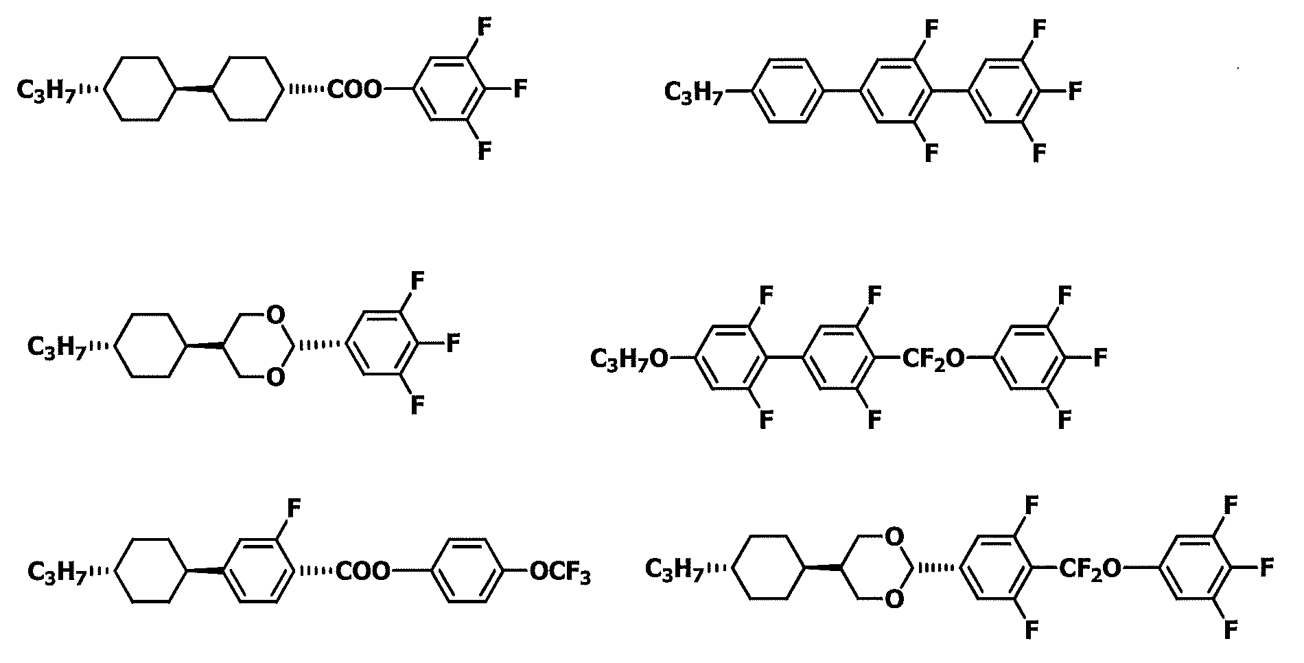
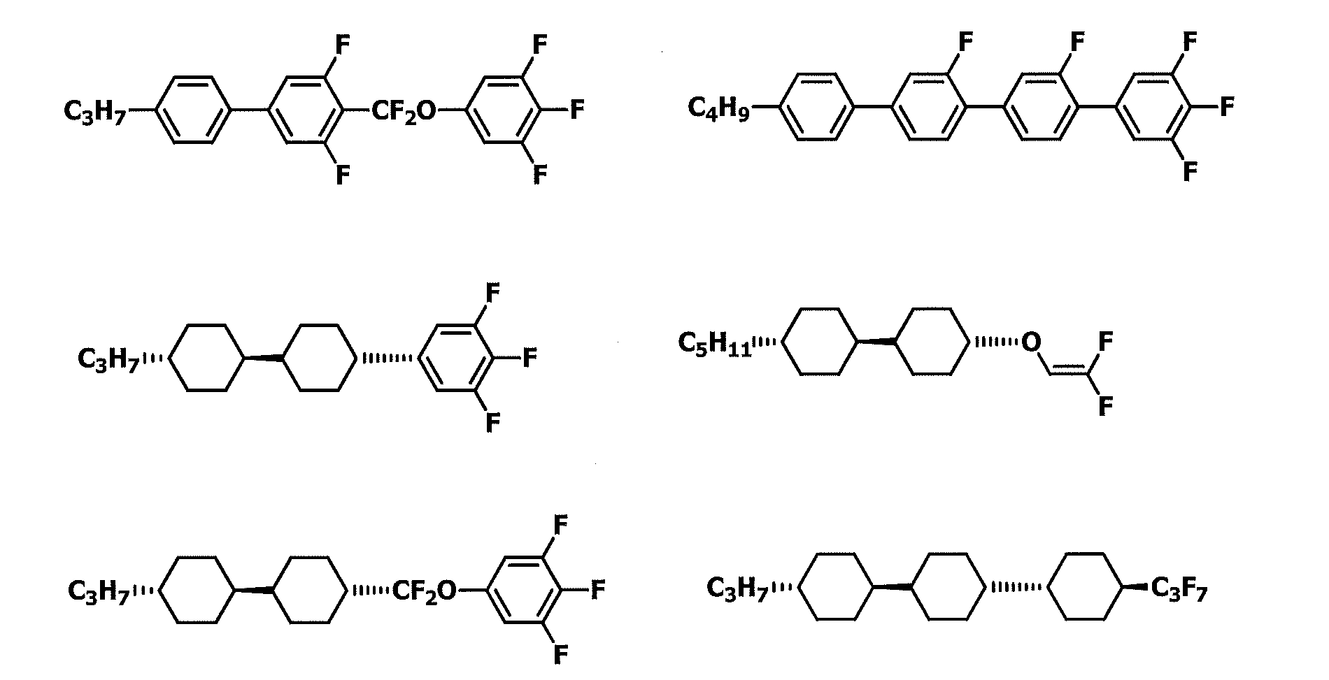
具体的には、低分子液晶として、4-シアノ-4’-n-ペンチルビフェニル、4-シアノ-4’-n-フェプチロキシビフェニル等のシアノビフェニル類;コレステリルアセテート、コレステリルベンゾエート等のコレステリルエステル類;4-カ ルボキシフェニルエチルカーボネート、4-カルボキシフェニル-n-ブチルカーボネート等の炭酸エステル類;安息香酸フェニルエステル、フタル酸ビフェニ ルエステル等のフェニルエステル類;ベンジリデン-2-ナフチルアミン、4’-n-ブトキシベンジリデン-4-アセチルアニリン等のシッフ塩基類;N,N’-ビスベンジリデンベンジジン、p-ジアニスアルベンジジン等のベンジジン類;4,4’-アゾキシジアニソール、4,4’-ジ-n-ブトキシ アゾキシベンゼン等のアゾキシベンゼン類;以下に具体的に示すフェニルシクロヘキシル系、ターフェニル系、フェニルビシクロヘキシル系などの液晶;などを挙げることができるがこれらに限定されない。

上述の光反応性高分子膜は、(A-1)光架橋、及び(A-2)光異性化からなる群から選ばれる少なくとも1種の反応を生じる光反応性側鎖を有する光反応性高分子を有して形成されるのがよい。
なお、本明細書において光反応性とは、(A-1)光架橋、又は(A-2)光異性化、のいずれかの反応;及び双方の反応;を生じる性質をいう。
光反応性高分子は、好ましくは(A-1)光架橋反応を生じる側鎖を有するのがよい。
光反応性高分子は、ii)250nm~450nmの波長範囲の光で反応し、かつ50~300℃の温度範囲で液晶性を示すのがよい。
光反応性高分子は、iii)250nm~450nmの波長範囲の光、特に偏光紫外線に反応する光反応性側鎖を有することが好ましい。
光反応性高分子は、iv)50~300℃の温度範囲で液晶性を示すためメソゲン基を有することが好ましい。
光反応性高分子の側鎖の構造は、剛直なメソゲン成分を有する方が、液晶の配向が安定するため、好ましい。
また、光反応性高分子の側鎖として、下記式(1)~(6)の少なくとも1種からなる側鎖であるのが好ましい。

Sは、炭素数1~12のアルキレン基であり、それらに結合する水素原子はハロゲン基に置き換えられていてもよい;
Tは、単結合または炭素数1~12のアルキレン基であり、それらに結合する水素原子はハロゲン基に置き換えられていてもよい;
Y1は、1価のベンゼン環、ナフタレン環、ビフェニル環、フラン環、ピロール環および炭素数5~8の脂環式炭化水素から選ばれる環を表すか、それらの置換基から選ばれる同一又は相異なった2~6の環が結合基Bを介して結合してなる基であり、それらに結合する水素原子はそれぞれ独立に-COOR0(式中、R0は水素原子又は炭素数1~5のアルキル基を表す)、-NO2、-CN、-CH=C(CN)2、-CH=CH-CN、ハロゲン基、炭素数1~5のアルキル基、又は炭素数1~5のアルキルオキシ基で置換されても良い;
Y2は、2価のベンゼン環、ナフタレン環、ビフェニル環、フラン環、ピロール環、炭素数5~8の脂環式炭化水素、および、それらの組み合わせからなる群から選ばれる基であり、それらに結合する水素原子はそれぞれ独立に-NO2、-CN、-CH=C(CN)2、-CH=CH-CN、ハロゲン基、炭素数1~5のアルキル基、又は炭素数1~5のアルキルオキシ基で置換されても良い;
Rは、ヒドロキシ基、炭素数1~6のアルコキシ基を表すか、又はY1と同じ定義を表す;
Xは、単結合、-COO-、-OCO-、-N=N-、-CH=CH-、-C≡C-、-CH=CH-CO-O-、又は-O-CO-CH=CH-を表し、Xの数が2となるときは、X同士は同一でも異なっていてもよい;
Couは、クマリン-6-イル基またはクマリン-7-イル基を表し、それらに結合する水素原子はそれぞれ独立に-NO2、-CN、-CH=C(CN)2、-CH=CH-CN、ハロゲン基、炭素数1~5のアルキル基、又は炭素数1~5のアルキルオキシ基で置換されても良い;
q1とq2は、一方が1で他方が0である;
q3は0または1である;
P及びQは、各々独立に、2価のベンゼン環、ナフタレン環、ビフェニル環、フラン環、ピロール環、炭素数5~8の脂環式炭化水素、および、それらの組み合わせからなる群から選ばれる基である;ただし、Xが-CH=CH-CO-O-、-O-CO-CH=CH-である場合、-CH=CH-が結合する側のP又はQは芳香環であり、Pの数が2以上となるときは、P同士は同一でも異なっていてもよく、Qの数が2以上となるときは、Q同士は同一でも異なっていてもよい;
l1は0または1である;
l2は0~2の整数である;
l1とl2がともに0であるときは、Tが単結合であるときはAも単結合を表す;
l1が1であるときは、Tが単結合であるときはBも単結合を表す;
H及びIは、各々独立に、2価のベンゼン環、ナフタレン環、ビフェニル環、フラン環、ピロール環、およびそれらの組み合わせから選ばれる基である。
式中、A、B、D、Y1、X、Y2、及びRは、上記と同じ定義を有する;
lは1~12の整数を表す;
mは、0~2の整数を表し、m1、m2は1~3の整数を表す;
nは0~12の整数(ただしn=0のときBは単結合である)を表す。

式中、A、X、l、m、m1及びRは、上記と同じ定義を有する。
式中、A、Y1、l、m1及びm2は上記と同じ定義を有する。

式中、A、X、l及びmは、上記と同じ定義を有する。
(式中、A、B、Y1、R1は、上記と同じ定義を有する。
q1とq2は、一方が1で他方が0である;
lは1~12の整数を表し、m1、m2は1~3の整数を表す;
式中、A、Y1、X、l及びmは上記と同じ定義を有する。

式中、A、B、q1及びq2は上記と同じ定義を有する;
Y3は、1価のベンゼン環、ナフタレン環、ビフェニル環、フラン環、窒素含有複素環、及び炭素数5~8の脂環式炭化水素、および、それらの組み合わせからなる群から選ばれる基であり、それらに結合する水素原子はそれぞれ独立に-NO2、-CN、ハロゲン基、炭素数1~5のアルキル基、又は炭素数1~5のアルキルオキシ基で置換されても良い;
R3は、水素原子、-NO2、-CN、-CH=C(CN)2、-CH=CH-CN、ハロゲン基、1価のベンゼン環、ナフタレン環、ビフェニル環、フラン環、窒素含有複素環、炭素数5~8の脂環式炭化水素、炭素数1~12のアルキル基、又は炭素数1~12のアルコキシ基を表す;
lは1~12の整数を表し、mは0から2の整数を表し、但し、式(23)~(24)において、全てのmの合計は2以上であり、式(25)~(26)において、全てのmの合計は1以上であり、m1、m2およびm3は、それぞれ独立に1~3の整数を表す;
R2は、水素原子、-NO2、-CN、ハロゲン基、1価のベンゼン環、ナフタレン環、ビフェニル環、フラン環、窒素含有複素環、及び炭素数5~8の脂環式炭化水素、および、アルキル基、又はアルキルオキシ基を表す;
Z1、Z2は単結合、-CO-、-CH2O-、-CH=N-、-CF2-を表す。

上述の光反応性高分子膜は、上記光反応性側鎖を有する光反応性側鎖モノマーを重合することによって、場合によっては該光反応性側鎖モノマーと上記液晶性側鎖を有するモノマーとを共重合することによって、得ることができる。例えば、WO2017/061536号公報(該公報の内容は全て、参照により本願に組み込まれる)の[0062]~[0090]を参照することによって、製造することができる。
本発明の偏光撮像装置は、レンズ素子を有する。該レンズ素子は、後述する受光素子において結像する作用を有すれば、特に限定されない。
<受光素子>
本発明の偏光撮像装置は、受光素子を有する。該受光素子は、結像したデータから上述のS0~S3を求めることができれば、特に限定されない。
図3は、本発明の偏光撮像装置の概略を説明する図である。
本発明の偏光撮像装置は、結像レンズ、色フィルタ、異方性回折格子、受光素子アレイを有して成る。
結像レンズは受光素子アレイからの配置距離を可変とし、ピント調整できるようにしている。
異方性回折格子の回折角は波長依存性を伴うため、白色光に対しては角度分散によって像がボケる問題が生じ得る。このため、色フィルタを挿入して分散の影響を低減している。異方性回折格子は観測波長に応じてリタデーションが最適化されたものを対応する周波数帯の干渉フィルタと組み合わせて用いる。
一般にストークスパラメータを求めるには、式(1)にある0deg直線偏光成分、90deg直線偏光成分、45deg直線偏光成分、-45deg直線偏光成分、右回り円偏光成分、左回り円偏光成分の各光強度を測定する方法や、回転移相子法などのフーリエ解析法が用いられる。しかし、これらの手法では、原理上複数回の測定を要するため、状態が時間的に変化するような被写体の測定には向かない。
これに対し、本発明の偏光撮像装置では、ストークスパラメータの計測に必要な情報を空間的に分離し、強度情報として一度に取得することで、スナップショットでの偏光イメージング計測を可能としている。即ち、動的な被測定対象であっても測定可能であることを特徴としている。また、回折格子を含めて高額な光学素子を要しないため、安価である点も特徴のひとつである。
以下、本発明について、実施例を用いて具体的に説明するが、本発明は該実施例によってのみ限定されるものではない。
記録材料として、下記式で表される光架橋性高分子液晶(4-(4-methoxycinnamoyloxy)biphenyl side groups(P6CB))を用いた。
P6CBをジクロロメタンに溶解し、ガラス基板上に膜厚が300nmとなるようにスピンコートした。
P6CBフィルムがコートされたガラス基板を2枚用意し、P6CBフィルム側を対向させて張り合わせて空のセルを作成した。作製した空セルに、He-Cdレーザから射出された波長325nmの紫外レーザをOC干渉させながら600mJ/cm2の露光エネルギーで照射した。照射後に150℃のオーブンで15分間熱処理し、熱処理後に低分子液晶5CB(4-cyano-4'-pentylbiphenyl)をセル内に注入してセルタイプのOC格子を作製した。作製した異方性回折格子の直径は8mmであった。
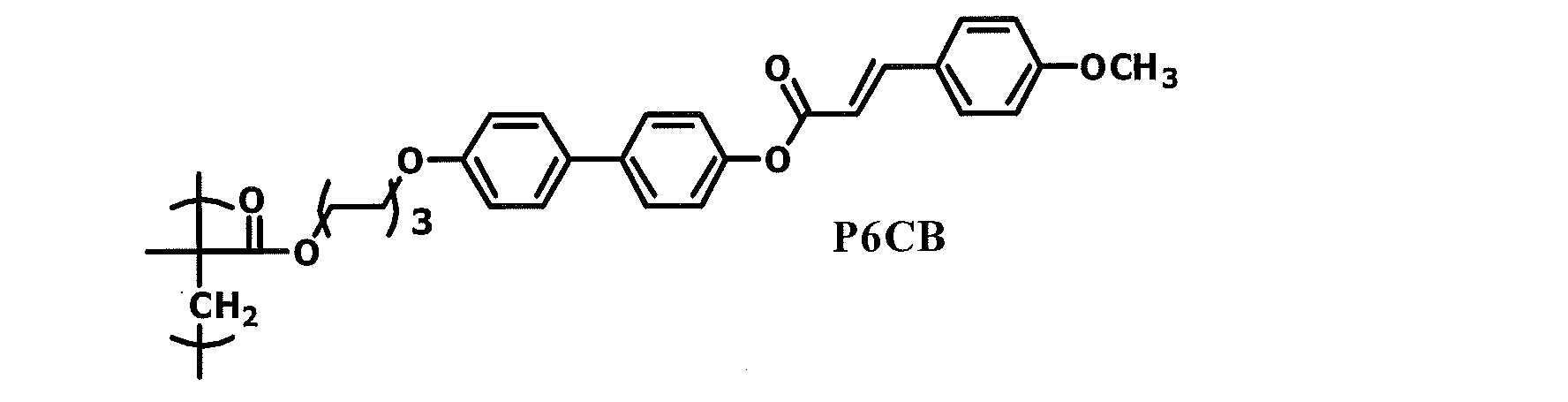
図3に示す偏光撮像装置の概略図に従って、偏光撮像装置を作製した。
具体的には、図4に示すように、偏光撮像装置は、被写体から順に、結像レンズ、干渉フィルタ(Throrlabs社製FL532-3(中心波長532nm)、上記で得た異方性回折格子、及び受光素子となるように配置した。なお、受光素子として市販カメラ(SONY社製ILCE6000S)を用い、結像レンズ、干渉フィルタ、及び異方性回折格子はゲージシステムにパッケージ化し、該市販カメラに装着できるように設計した。
本実施例では、円偏光に対する選択反射特性を示すコガネムシを被写体として用い、イメージング計測を行った。その画像を図5に示す。
図5から3つの画像スポットが得られていることがわかる。左から順に、OC格子の-1次光、0次光、+1次光成分に該当する。このうち、-1次光と+1次光成分が左回り円偏光成分と右回り円偏光成分の2次元分布を表している。
-1次光成分(I-1)と+1次光成分(I+1)の像を画像処理により抽出し、下記数式に基づいて差分計算を施して求めたS3のイメージング画像を図6に示す。

したがって、本発明の偏光撮像装置により、スナップショットでストークスパラメータの空間分布をイメージング計測できることが実証された。
Claims (15)
- 光学異方性が周期的に変調された異方性回折格子素子、レンズ素子、及び受光素子を有する偏光撮像装置。
- 前記異方性回折格子素子が、互いに方向の異なる複数個の格子ベクトルを有する異方性回折格子を有し、前記格子ベクトルは少なくとも異方性方位又は複屈折が周期的に変調される、請求項1記載の装置。
- 前記異方性回折格子素子が、入射光のストークスパラメータの情報を、異方性方位および複屈折の分布に応じて空間的に分離し、強度情報へと変換する異方性回折格子を有する、請求項1又は請求項2記載の装置。
- 前記異方性回折格子素子が、(A-1)光架橋、及び(A-2)光異性化からなる群から選ばれる少なくとも1種の反応を生じる光反応性側鎖を有する光反応性高分子膜を有する異方性回折格子を含む請求項1~3のいずれか1項記載の装置。
- 前記異方性回折格子素子が、前記光反応性高分子膜からなる異方性回折格子を含む請求項1~4のいずれか1項記載の装置。
- 前記異方性回折格子素子が、
I)第1の透明基体層;及び
II)(A-1)光架橋、及び(A-2)光異性化からなる群から選ばれる少なくとも1種の反応を生じる第1の光反応性側鎖を有する第1の光反応性高分子膜
を有する異方性回折格子を含む請求項1~5のいずれか1項記載の装置。 - 前記異方性回折格子素子が、
III)第2の透明基体層;及び
IV)(A-1)光架橋、及び(A-2)光異性化からなる群から選ばれる少なくとも1種の反応を生じる第2の光反応性側鎖を有する第2の光反応性高分子膜;及び
を有し、
前記II)第1の光反応性高分子膜と前記IV)第2の光反応性高分子膜とが対向するように配置し、前記II)第1の膜及び前記IV)第2の膜の間に、(B)低分子液晶層が配置される異方性回折格子を含む請求項1~4及び6のいずれか1項記載の装置。 - 前記光反応性高分子膜に所望の偏光を干渉露光し、該高分子薄膜に任意の回折パターンを形成することで、該高分子薄膜に入射する光のストークスパラメータの情報を、該高分子薄膜に形成された異方性方位および複屈折の分布に応じて空間的に分離し、強度情報へと変換する異方性回折格子とする請求項4~7のいずれか1項記載の装置。
- 前記光反応性高分子膜が、下記式(1)~(6)
(式中、A、B、Dはそれぞれ独立に、単結合、-O-、-CH2-、-COO-、-OCO-、-CONH-、-NH-CO-、-CH=CH-CO-O-、又は-O-CO-CH=CH-を表す;
Sは、炭素数1~12のアルキレン基であり、それらに結合する水素原子はハロゲン基に置き換えられていてもよい;
Tは、単結合または炭素数1~12のアルキレン基であり、それらに結合する水素原子はハロゲン基に置き換えられていてもよい;
Y1は、1価のベンゼン環、ナフタレン環、ビフェニル環、フラン環、ピロール環および炭素数5~8の脂環式炭化水素から選ばれる環を表すか、それらの置換基から選ばれる同一又は相異なった2~6の環が結合基Bを介して結合してなる基であり、それらに結合する水素原子はそれぞれ独立に-COOR0(式中、R0は水素原子又は炭素数1~5のアルキル基を表す)、-NO2、-CN、-CH=C(CN)2、-CH=CH-CN、ハロゲン基、炭素数1~5のアルキル基、又は炭素数1~5のアルキルオキシ基で置換されても良い;
Y2は、2価のベンゼン環、ナフタレン環、ビフェニル環、フラン環、ピロール環、炭素数5~8の脂環式炭化水素、および、それらの組み合わせからなる群から選ばれる基であり、それらに結合する水素原子はそれぞれ独立に-NO2、-CN、-CH=C(CN)2、-CH=CH-CN、ハロゲン基、炭素数1~5のアルキル基、又は炭素数1~5のアルキルオキシ基で置換されても良い;
Rは、ヒドロキシ基、炭素数1~6のアルコキシ基を表すか、又はY1と同じ定義を表す;
Xは、単結合、-COO-、-OCO-、-N=N-、-CH=CH-、-C≡C-、-CH=CH-CO-O-、又は-O-CO-CH=CH-を表し、Xの数が2となるときは、X同士は同一でも異なっていてもよい;
Couは、クマリン-6-イル基またはクマリン-7-イル基を表し、それらに結合する水素原子はそれぞれ独立に-NO2、-CN、-CH=C(CN)2、-CH=CH-CN、ハロゲン基、炭素数1~5のアルキル基、又は炭素数1~5のアルキルオキシ基で置換されても良い;
q1とq2は、一方が1で他方が0である;
q3は0または1である;
P及びQは、各々独立に、2価のベンゼン環、ナフタレン環、ビフェニル環、フラン環、ピロール環、炭素数5~8の脂環式炭化水素、および、それらの組み合わせからなる群から選ばれる基である;ただし、Xが-CH=CH-CO-O-、-O-CO-CH=CH-である場合、-CH=CH-が結合する側のP又はQは芳香環であり、Pの数が2以上となるときは、P同士は同一でも異なっていてもよく、Qの数が2以上となるときは、Q同士は同一でも異なっていてもよい;
l1は0または1である;
l2は0~2の整数である;
l1とl2がともに0であるときは、Tが単結合であるときはAも単結合を表す;
l1が1であるときは、Tが単結合であるときはBも単結合を表す;
H及びIは、各々独立に、2価のベンゼン環、ナフタレン環、ビフェニル環、フラン環、ピロール環、およびそれらの組み合わせから選ばれる基である。)
からなる群から選ばれるいずれか1種の光反応性側鎖を有する光反応性高分子を有する請求項4~8のいずれか1項に記載の装置。

- 前記光反応性高分子膜が、下記式(7)~(10)
(式中、A、B、Dはそれぞれ独立に、単結合、-O-、-CH2-、-COO-、-OCO-、-CONH-、-NH-CO-、-CH=CH-CO-O-、又は-O-CO-CH=CH-を表す;
Y1は、1価のベンゼン環、ナフタレン環、ビフェニル環、フラン環、ピロール環および炭素数5~8の脂環式炭化水素から選ばれる環を表すか、それらの置換基から選ばれる同一又は相異なった2~6の環が結合基Bを介して結合してなる基であり、それらに結合する水素原子はそれぞれ独立に-COOR0(式中、R0は水素原子又は炭素数1~5のアルキル基を表す)、-NO2、-CN、-CH=C(CN)2、-CH=CH-CN、ハロゲン基、炭素数1~5のアルキル基、又は炭素数1~5のアルキルオキシ基で置換されても良い;
Xは、単結合、-COO-、-OCO-、-N=N-、-CH=CH-、-C≡C-、-CH=CH-CO-O-、又は-O-CO-CH=CH-を表し、Xの数が2となるときは、X同士は同一でも異なっていてもよい;
lは1~12の整数を表す;
mは、0~2の整数を表し、m1、m2は1~3の整数を表す;
nは0~12の整数(ただしn=0のときBは単結合である)を表す;
Y2は、2価のベンゼン環、ナフタレン環、ビフェニル環、フラン環、ピロール環、炭素数5~8の脂環式炭化水素、および、それらの組み合わせからなる群から選ばれる基であり、それらに結合する水素原子はそれぞれ独立に-NO2、-CN、-CH=C(CN)2、-CH=CH-CN、ハロゲン基、炭素数1~5のアルキル基、又は炭素数1~5のアルキルオキシ基で置換されても良い;
Rは、ヒドロキシ基、炭素数1~6のアルコキシ基を表すか、又はY1と同じ定義を表す)
からなる群から選ばれるいずれか1種の光反応性側鎖を有する光反応性高分子を有する請求項4~8のいずれか1項に記載の装置。

- 前記光反応性高分子膜が、下記式(11)~(13)
(式中、Aは、それぞれ独立に、単結合、-O-、-CH2-、-COO-、-OCO-、-CONH-、-NH-CO-、-CH=CH-CO-O-、又は-O-CO-CH=CH-を表す;
Xは、単結合、-COO-、-OCO-、-N=N-、-CH=CH-、-C≡C-、-CH=CH-CO-O-、又は-O-CO-CH=CH-を表し、Xの数が2となるときは、X同士は同一でも異なっていてもよい;
lは、1~12の整数を表し、mは0~2の整数を表し、m1は1~3の整数を表す;
Rは、1価のベンゼン環、ナフタレン環、ビフェニル環、フラン環、ピロール環および炭素数5~8の脂環式炭化水素から選ばれる環を表すか、それらの置換基から選ばれる同一又は相異なった2~6の環が結合基Bを介して結合してなる基であり、それらに結合する水素原子はそれぞれ独立に-COOR0(式中、R0は水素原子又は炭素数1~5のアルキル基を表す)、-NO2、-CN、-CH=C(CN)2、-CH=CH-CN、ハロゲン基、炭素数1~5のアルキル基、又は炭素数1~5のアルキルオキシ基で置換されても良いか、又はヒドロキシ基もしくは炭素数1~6のアルコキシ基を表す)
からなる群から選ばれるいずれか1種の光反応性側鎖を有する光反応性高分子を有する請求項4~8のいずれか1項に記載の装置。
- 前記光反応性高分子膜が、下記式(14)又は(15)
(式中、Aはそれぞれ独立に、単結合、-O-、-CH2-、-COO-、-OCO-、-CONH-、-NH-CO-、-CH=CH-CO-O-、又は-O-CO-CH=CH-を表す;
Y1は、1価のベンゼン環、ナフタレン環、ビフェニル環、フラン環、ピロール環および炭素数5~8の脂環式炭化水素から選ばれる環を表すか、それらの置換基から選ばれる同一又は相異なった2~6の環が結合基Bを介して結合してなる基であり、それらに結合する水素原子はそれぞれ独立に-COOR0(式中、R0は水素原子又は炭素数1~5のアルキル基を表す)、-NO2、-CN、-CH=C(CN)2、-CH=CH-CN、ハロゲン基、炭素数1~5のアルキル基、又は炭素数1~5のアルキルオキシ基で置換されても良い;
lは1~12の整数を表し、m1、m2は1~3の整数を表す)
で表される光反応性側鎖を有する光反応性高分子を有する請求項4~8のいずれか1項に記載の装置。
- 前記光反応性高分子膜が、下記式(16)又は(17)(式中、Aは単結合、-O-、-CH2-、-COO-、-OCO-、-CONH-、-NH-CO-、-CH=CH-CO-O-、又は-O-CO-CH=CH-を表す;
Xは、単結合、-COO-、-OCO-、-N=N-、-CH=CH-、-C≡C-、-CH=CH-CO-O-、又は-O-CO-CH=CH-を表し、Xの数が2となるときは、X同士は同一でも異なっていてもよい;
lは、1~12の整数を表し、mは0~2の整数を表す)
で表される光反応性側鎖を有する光反応性高分子を有する請求項4~8のいずれか1項に記載の装置。

- 前記光反応性高分子膜が、下記式(18)又は(19)
(式中、A、Bはそれぞれ独立に、単結合、-O-、-CH2-、-COO-、-OCO-、-CONH-、-NH-CO-、-CH=CH-CO-O-、又は-O-CO-CH=CH-を表す;
Y1は、1価のベンゼン環、ナフタレン環、ビフェニル環、フラン環、ピロール環および炭素数5~8の脂環式炭化水素から選ばれる環を表すか、それらの置換基から選ばれる同一又は相異なった2~6の環が結合基Bを介して結合してなる基であり、それらに結合する水素原子はそれぞれ独立に-COOR0(式中、R0は水素原子又は炭素数1~5のアルキル基を表す)、-NO2、-CN、-CH=C(CN)2、-CH=CH-CN、ハロゲン基、炭素数1~5のアルキル基、又は炭素数1~5のアルキルオキシ基で置換されても良い;
q1とq2は、一方が1で他方が0である;
lは1~12の整数を表し、m1、m2は1~3の整数を表す;
R1は、水素原子、-NO2、-CN、-CH=C(CN)2、-CH=CH-CN、ハロゲン基、炭素数1~5のアルキル基、又は炭素数1~5のアルキルオキシ基を表す)
からなる群から選ばれるいずれか1種の感光性側鎖を有する光反応性高分子を有する請求項4~8のいずれか1項に記載の装置。

- 前記光反応性高分子膜が、下記式(20)
(式中、Aは、単結合、-O-、-CH2-、-COO-、-OCO-、-CONH-、-NH-CO-、-CH=CH-CO-O-、又は-O-CO-CH=CH-を表す;
Y1は、1価のベンゼン環、ナフタレン環、ビフェニル環、フラン環、ピロール環および炭素数5~8の脂環式炭化水素から選ばれる環を表すか、それらの置換基から選ばれる同一又は相異なった2~6の環が結合基Bを介して結合してなる基であり、それらに結合する水素原子はそれぞれ独立に-COOR0(式中、R0は水素原子又は炭素数1~5のアルキル基を表す)、-NO2、-CN、-CH=C(CN)2、-CH=CH-CN、ハロゲン基、炭素数1~5のアルキル基、又は炭素数1~5のアルキルオキシ基で置換されても良い;
Xは、単結合、-COO-、-OCO-、-N=N-、-CH=CH-、-C≡C-、-CH=CH-CO-O-、又は-O-CO-CH=CH-を表し、Xの数が2となるときは、X同士は同一でも異なっていてもよい;
lは1~12の整数を表し、mは0~2の整数を表す)で表される光反応性側鎖を有する光反応性高分子を有する請求項4~8のいずれか1項に記載の装置。

Priority Applications (3)
| Application Number | Priority Date | Filing Date | Title |
|---|---|---|---|
| JP2019537643A JP7101356B2 (ja) | 2017-08-23 | 2018-08-22 | 偏光撮像装置 |
| KR1020207007575A KR102645233B1 (ko) | 2017-08-23 | 2018-08-22 | 편광 촬상 장치 |
| CN201880068721.2A CN111247405B (zh) | 2017-08-23 | 2018-08-22 | 偏振摄像装置 |
Applications Claiming Priority (2)
| Application Number | Priority Date | Filing Date | Title |
|---|---|---|---|
| JP2017-160221 | 2017-08-23 | ||
| JP2017160221 | 2017-08-23 |
Publications (1)
| Publication Number | Publication Date |
|---|---|
| WO2019039486A1 true WO2019039486A1 (ja) | 2019-02-28 |
Family
ID=65439885
Family Applications (1)
| Application Number | Title | Priority Date | Filing Date |
|---|---|---|---|
| PCT/JP2018/030902 Ceased WO2019039486A1 (ja) | 2017-08-23 | 2018-08-22 | 偏光撮像装置 |
Country Status (5)
| Country | Link |
|---|---|
| JP (1) | JP7101356B2 (ja) |
| KR (1) | KR102645233B1 (ja) |
| CN (1) | CN111247405B (ja) |
| TW (1) | TWI838344B (ja) |
| WO (1) | WO2019039486A1 (ja) |
Cited By (3)
| Publication number | Priority date | Publication date | Assignee | Title |
|---|---|---|---|---|
| JP2020204539A (ja) * | 2019-06-18 | 2020-12-24 | 国立大学法人長岡技術科学大学 | 偏光撮像装置 |
| WO2021261541A1 (ja) * | 2020-06-25 | 2021-12-30 | 国立大学法人長岡技術科学大学 | 偏光撮像装置 |
| JP2023102081A (ja) * | 2022-01-11 | 2023-07-24 | 林テレンプ株式会社 | 偏光回折素子および偏光解析装置 |
Citations (5)
| Publication number | Priority date | Publication date | Assignee | Title |
|---|---|---|---|---|
| JP2007121235A (ja) * | 2005-10-31 | 2007-05-17 | Nagaoka Univ Of Technology | 偏光回折素子を用いた機械駆動不要な偏光解析システム |
| JP2007304215A (ja) * | 2006-05-09 | 2007-11-22 | Hayashi Telempu Co Ltd | 光配向材および光学素子、液晶配向膜の製造方法 |
| US20120268745A1 (en) * | 2011-04-20 | 2012-10-25 | Arizona Board Of Regents On Behalf Of The University Of Arizona | Ultra-compact snapshot imaging fourier transform spectrometer |
| WO2016031567A1 (ja) * | 2014-08-26 | 2016-03-03 | 学校法人同志社 | 複屈折測定装置および複屈折測定方法 |
| WO2017061536A1 (ja) * | 2015-10-07 | 2017-04-13 | 公立大学法人兵庫県立大学 | 光学素子及びその製造方法 |
-
2018
- 2018-08-22 CN CN201880068721.2A patent/CN111247405B/zh active Active
- 2018-08-22 JP JP2019537643A patent/JP7101356B2/ja active Active
- 2018-08-22 TW TW107129213A patent/TWI838344B/zh active
- 2018-08-22 WO PCT/JP2018/030902 patent/WO2019039486A1/ja not_active Ceased
- 2018-08-22 KR KR1020207007575A patent/KR102645233B1/ko active Active
Patent Citations (5)
| Publication number | Priority date | Publication date | Assignee | Title |
|---|---|---|---|---|
| JP2007121235A (ja) * | 2005-10-31 | 2007-05-17 | Nagaoka Univ Of Technology | 偏光回折素子を用いた機械駆動不要な偏光解析システム |
| JP2007304215A (ja) * | 2006-05-09 | 2007-11-22 | Hayashi Telempu Co Ltd | 光配向材および光学素子、液晶配向膜の製造方法 |
| US20120268745A1 (en) * | 2011-04-20 | 2012-10-25 | Arizona Board Of Regents On Behalf Of The University Of Arizona | Ultra-compact snapshot imaging fourier transform spectrometer |
| WO2016031567A1 (ja) * | 2014-08-26 | 2016-03-03 | 学校法人同志社 | 複屈折測定装置および複屈折測定方法 |
| WO2017061536A1 (ja) * | 2015-10-07 | 2017-04-13 | 公立大学法人兵庫県立大学 | 光学素子及びその製造方法 |
Cited By (7)
| Publication number | Priority date | Publication date | Assignee | Title |
|---|---|---|---|---|
| JP2020204539A (ja) * | 2019-06-18 | 2020-12-24 | 国立大学法人長岡技術科学大学 | 偏光撮像装置 |
| JP7440845B2 (ja) | 2019-06-18 | 2024-02-29 | 国立大学法人長岡技術科学大学 | 偏光撮像装置 |
| WO2021261541A1 (ja) * | 2020-06-25 | 2021-12-30 | 国立大学法人長岡技術科学大学 | 偏光撮像装置 |
| JPWO2021261541A1 (ja) * | 2020-06-25 | 2021-12-30 | ||
| JP7776082B2 (ja) | 2020-06-25 | 2025-11-26 | 国立大学法人長岡技術科学大学 | 偏光撮像装置 |
| JP2023102081A (ja) * | 2022-01-11 | 2023-07-24 | 林テレンプ株式会社 | 偏光回折素子および偏光解析装置 |
| JP7823826B2 (ja) | 2022-01-11 | 2026-03-04 | 林テレンプ株式会社 | 偏光回折素子および偏光解析装置 |
Also Published As
| Publication number | Publication date |
|---|---|
| CN111247405A (zh) | 2020-06-05 |
| TWI838344B (zh) | 2024-04-11 |
| JP7101356B2 (ja) | 2022-07-15 |
| JPWO2019039486A1 (ja) | 2020-10-15 |
| CN111247405B (zh) | 2022-10-18 |
| KR20200044026A (ko) | 2020-04-28 |
| KR102645233B1 (ko) | 2024-03-07 |
| TW201920307A (zh) | 2019-06-01 |
Similar Documents
| Publication | Publication Date | Title |
|---|---|---|
| Escuti et al. | Simplified spectropolarimetry using reactive mesogen polarization gratings | |
| US10036886B2 (en) | Broadband optics for manipulating light beams and images | |
| KR101506949B1 (ko) | 기판들 상의 액정 편광 격자들의 제조 방법들 및 관련된 소자들 | |
| JP5669964B2 (ja) | 低ツイストキラル液晶偏光回折格子および関連する作製方法 | |
| Sakhno et al. | Fabrication and performance of efficient thin circular polarization gratings with Bragg properties using bulk photo-alignment of a liquid crystalline polymer | |
| KR102645233B1 (ko) | 편광 촬상 장치 | |
| JP7555356B2 (ja) | ハイパースペクトルセンサー、ハイパースペクトルカメラ | |
| Labarthet et al. | Photoinduced orientations of azobenzene chromophores in two distinct holographic diffraction gratings as studied by polarized Raman confocal microspectrometry | |
| JP7776082B2 (ja) | 偏光撮像装置 | |
| US5638207A (en) | Flare-prevention optical system, flare-prevention method, and flying height tester | |
| JP7440845B2 (ja) | 偏光撮像装置 | |
| JP7541104B2 (ja) | 透過型液晶回折素子 | |
| Evans et al. | Bragg-matched photorefractive two-beam coupling in organic–inorganic hybrids | |
| JP2012073522A (ja) | 位相型回折素子、その製造方法、および撮像装置 | |
| Golicha et al. | Optical techniques in the determination of pitch lengths in the cholesteric and chiral smectic C phases | |
| JP5169165B2 (ja) | 化合物、液晶組成物、光学異方性材料および光学素子 | |
| US20230125215A1 (en) | Optically anisotropic film, optical element, and optical system | |
| JP7561828B2 (ja) | 液晶層の製造方法 | |
| Khos-Ochir et al. | Polarimetric measurement of Jones matrix of a twisted nematic liquid crystal spatial light modulator | |
| WO2023085398A1 (ja) | 光学素子、および、画像表示装置 | |
| WO2023282085A1 (ja) | 分光器 | |
| Bjorknas et al. | Quantitative conoscopic imaging of cholesteric thin films | |
| JP7545296B2 (ja) | 画像表示システム | |
| US20250224546A1 (en) | Liquid crystal diffraction element | |
| Heynderickx et al. | Liquid‐crystalline ordering in polymeric networks as studied by polarized raman scattering |
Legal Events
| Date | Code | Title | Description |
|---|---|---|---|
| 121 | Ep: the epo has been informed by wipo that ep was designated in this application |
Ref document number: 18848558 Country of ref document: EP Kind code of ref document: A1 |
|
| ENP | Entry into the national phase |
Ref document number: 2019537643 Country of ref document: JP Kind code of ref document: A |
|
| NENP | Non-entry into the national phase |
Ref country code: DE |
|
| ENP | Entry into the national phase |
Ref document number: 20207007575 Country of ref document: KR Kind code of ref document: A |
|
| 122 | Ep: pct application non-entry in european phase |
Ref document number: 18848558 Country of ref document: EP Kind code of ref document: A1 |