WO2019026705A1 - 液晶表示装置の製造方法 - Google Patents
液晶表示装置の製造方法 Download PDFInfo
- Publication number
- WO2019026705A1 WO2019026705A1 PCT/JP2018/027791 JP2018027791W WO2019026705A1 WO 2019026705 A1 WO2019026705 A1 WO 2019026705A1 JP 2018027791 W JP2018027791 W JP 2018027791W WO 2019026705 A1 WO2019026705 A1 WO 2019026705A1
- Authority
- WO
- WIPO (PCT)
- Prior art keywords
- alignment film
- liquid crystal
- photo alignment
- crystal display
- film
- Prior art date
- Legal status (The legal status is an assumption and is not a legal conclusion. Google has not performed a legal analysis and makes no representation as to the accuracy of the status listed.)
- Ceased
Links
Classifications
-
- G—PHYSICS
- G02—OPTICS
- G02F—OPTICAL DEVICES OR ARRANGEMENTS FOR THE CONTROL OF LIGHT BY MODIFICATION OF THE OPTICAL PROPERTIES OF THE MEDIA OF THE ELEMENTS INVOLVED THEREIN; NON-LINEAR OPTICS; FREQUENCY-CHANGING OF LIGHT; OPTICAL LOGIC ELEMENTS; OPTICAL ANALOGUE/DIGITAL CONVERTERS
- G02F1/00—Devices or arrangements for the control of the intensity, colour, phase, polarisation or direction of light arriving from an independent light source, e.g. switching, gating or modulating; Non-linear optics
- G02F1/01—Devices or arrangements for the control of the intensity, colour, phase, polarisation or direction of light arriving from an independent light source, e.g. switching, gating or modulating; Non-linear optics for the control of the intensity, phase, polarisation or colour
- G02F1/13—Devices or arrangements for the control of the intensity, colour, phase, polarisation or direction of light arriving from an independent light source, e.g. switching, gating or modulating; Non-linear optics for the control of the intensity, phase, polarisation or colour based on liquid crystals, e.g. single liquid crystal display cells
-
- G—PHYSICS
- G02—OPTICS
- G02F—OPTICAL DEVICES OR ARRANGEMENTS FOR THE CONTROL OF LIGHT BY MODIFICATION OF THE OPTICAL PROPERTIES OF THE MEDIA OF THE ELEMENTS INVOLVED THEREIN; NON-LINEAR OPTICS; FREQUENCY-CHANGING OF LIGHT; OPTICAL LOGIC ELEMENTS; OPTICAL ANALOGUE/DIGITAL CONVERTERS
- G02F1/00—Devices or arrangements for the control of the intensity, colour, phase, polarisation or direction of light arriving from an independent light source, e.g. switching, gating or modulating; Non-linear optics
- G02F1/01—Devices or arrangements for the control of the intensity, colour, phase, polarisation or direction of light arriving from an independent light source, e.g. switching, gating or modulating; Non-linear optics for the control of the intensity, phase, polarisation or colour
- G02F1/13—Devices or arrangements for the control of the intensity, colour, phase, polarisation or direction of light arriving from an independent light source, e.g. switching, gating or modulating; Non-linear optics for the control of the intensity, phase, polarisation or colour based on liquid crystals, e.g. single liquid crystal display cells
- G02F1/133—Constructional arrangements; Operation of liquid crystal cells; Circuit arrangements
- G02F1/1333—Constructional arrangements; Manufacturing methods
- G02F1/1337—Surface-induced orientation of the liquid crystal molecules, e.g. by alignment layers
Definitions
- the present invention relates to a method of manufacturing a liquid crystal display. More specifically, the present invention relates to a method of manufacturing a liquid crystal display device having a photo alignment film.
- a liquid crystal display device generally has an alignment film which controls the alignment of liquid crystal molecules (see, for example, Patent Documents 1 and 2).
- the alignment film imparts an alignment regulating force to liquid crystal molecules by being subjected to alignment processing such as rubbing processing and photo alignment processing, for example.
- alignment processing such as rubbing processing and photo alignment processing
- the display quality may be degraded due to the dust generation from the rubbing cloth. Therefore, in recent years, a method of forming a photo alignment film by performing photo alignment processing of irradiating light such as ultraviolet light instead of rubbing processing has been studied.
- an alignment film material containing a polymer (polymer) of a carboxylic acid dianhydride having a cyclobutane skeleton and a diamine as a constituent material (photo alignment film material) of the photo alignment film
- the photo alignment treatment by polarized light irradiation When applied, decomposition of the polymer chain occurs along the direction of the fast axis of the polarized light, and a maleimide compound is formed as a decomposition product.
- the maleimide compound as a decomposition product does not independently contribute to the alignment control force of the photo alignment film, and is sublimed by baking after the photo alignment processing.
- the maleimide compound when the maleimide compound is not sufficiently sublimated and remains on the surface of the photo alignment film, the maleimide compound may drift and aggregate in the liquid crystal layer and then reattach to the surface of the photo alignment film. As a result, the orientation of the liquid crystal molecules may be disturbed from the aggregates of the maleimide compound as nuclei, that is, the anisotropy may be partially reduced and may appear as a bright spot.
- the substrate having the photo alignment film is subjected to a liquid contact treatment with the anisotropy improving liquid, but the inventor examined it.
- the anisotropy improvement liquid described in in particular, ozone water
- the anisotropy may be significantly reduced by simply using it, which may cause a problem of afterimage. And there was room for improvement.
- the invention described in Patent Document 2 is premised on manufacturing a liquid crystal display device having an inorganic alignment film, and there is room for improvement.
- the present invention is made in view of the above-mentioned present situation, and it aims at providing a manufacturing method of a liquid crystal display which controls generating of a bright point, controlling a fall of anisotropy.
- the inventors of the present invention have variously examined a method of manufacturing a liquid crystal display device which suppresses generation of a bright spot while suppressing a decrease in anisotropy, and the maleimide compound (degraded product generated after photo alignment treatment ) Was removed by washing. And it discovered that generation
- the present invention has been achieved in consideration of the fact that the above-mentioned problems can be solved in a remarkable manner.
- one embodiment of the present invention is a method of manufacturing a liquid crystal display device including a pair of substrates and a liquid crystal layer sandwiched between the pair of substrates, wherein at least one surface of the pair of substrates is A step (1) of forming a film of a photoalignment film material containing a polymer of a carboxylic acid dianhydride having a cyclobutane skeleton and a diamine, and a step of irradiating polarized light onto the film to form a photoalignment film (2) A process for producing a liquid crystal display comprising the step (3) of washing the photo alignment film with ozone water having a concentration of 5 ppm or less for 1 minute or less (hereinafter referred to as “first liquid crystal of the present invention It may be referred to as “a manufacturing method of a display device”.
- the method of manufacturing a liquid crystal display device may further include the step (4) of firing the photo alignment film after the step (3).
- the method of manufacturing a liquid crystal display further includes a step (4) of firing the photo alignment film between the step (2) and the step (3). It may be
- Another aspect of the present invention is a method of manufacturing a liquid crystal display device comprising a pair of substrates and a liquid crystal layer sandwiched between the pair of substrates, wherein at least one surface of the pair of substrates is A step (1) of forming a film of a photoalignment film material containing a polymer of a carboxylic acid dianhydride having a cyclobutane skeleton and a diamine, and a step of irradiating polarized light onto the film to form a photoalignment film (2)
- a process for producing a liquid crystal display comprising the step (3) of washing the photo alignment film with alkaline reducing water (hereinafter referred to as “the process for producing the second liquid crystal display of the present invention”) It may be said).
- the method of manufacturing a liquid crystal display device may further include the step (4) of firing the photo alignment film after the step (3).
- the method for manufacturing a liquid crystal display device further includes the step (4) of firing the photo alignment film between the step (2) and the step (3). May be included.
- the display mode of the liquid crystal display device may be an IPS mode or an FFS mode.
- the manufacturing method of the liquid crystal display device which suppresses generation
- X to Y means “X or more and Y or less”.
- Embodiment 1 relates to a method of manufacturing the first liquid crystal display device of the present invention.
- a film of a photoalignment film material is formed on at least one surface of a pair of substrates.
- the film made of the photo alignment film material may be formed by applying the photo alignment film material on at least one surface of the pair of substrates and then performing pre-baking (drying), main baking and the like as appropriate.
- the pair of substrates may be previously cleaned with water or the like.
- the application of the photoalignment film material may be performed by, for example, a method such as a flexographic printing method or an inkjet method.
- Pre-baking is a heat treatment to volatilize (dry) the solvent in the photo alignment film material.
- the solvent may be partially or completely removed.
- This firing is a heat treatment that promotes the thermochemical reaction (for example, imidization reaction) of the polymer (polymer) in the photo alignment film material, or completely evaporates the solvent in the photo alignment film material. And may be performed at a temperature higher than the pre-baking.
- the photo alignment film material is an alignment film material containing a polymer (polymer) of a carboxylic acid dianhydride having a cyclobutane skeleton and a diamine, that is, a photodegradable alignment film material.
- the photoalignment film material may further contain a solvent.
- the polymer of carboxylic acid dianhydride having a cyclobutane skeleton and a diamine in the photoalignment film material may contain a polyamic acid or a derivative thereof represented by the following chemical formula (1).
- this polyamic acid is a polymer of a carboxylic acid dianhydride having a cyclobutane skeleton and an aromatic diamine or an aliphatic diamine.
- R ′ represents an aromatic compound or an aliphatic compound.
- r 1 , r 2 , r 3 and r 4 independently represent a hydrogen atom or an organic group having 1 to 4 carbon atoms.
- n represents the degree of polymerization.
- R ′ represents an aromatic compound or an aliphatic compound.
- r 1 , r 2 , r 3 and r 4 independently represent a hydrogen atom or an organic group having 1 to 4 carbon atoms.
- n represents the degree of polymerization.
- a combination of a pair of substrates for example, a combination of a thin film transistor array substrate and a color filter substrate generally used in the field of liquid crystal display devices can be mentioned.
- polarized irradiation photoalignment treatment
- the polymer chains in the film by the photoalignment film material are decomposed and cut along the fast axis direction of polarized light.
- the film made of the photo alignment film material contains the polyimide represented by the above chemical formula (2)
- the polyimide along the fast axis direction of polarized light Is decomposed to form a maleimide compound represented by the following chemical formula (3) as a decomposition product.
- the maleimide compound as a decomposition product does not independently contribute to the alignment control force of the photo alignment film, but if it is largely left on the surface of the photo alignment film, it floats in the liquid crystal layer to be formed later and is aggregated. And re-adhered to the surface of the photo alignment film. As a result, the orientation of the liquid crystal molecules may be disturbed with the maleimide compound aggregate as a nucleus and may appear as a bright spot.
- the maleimide compound can be efficiently removed by washing the photo alignment film in a later step.
- R ′ represents an aromatic compound or an aliphatic compound.
- r 1 , r 2 , r 3 and r 4 independently represent a hydrogen atom or an organic group having 1 to 4 carbon atoms.
- n represents the degree of polymerization.
- Polarized irradiation may be performed through a wire grid polarizer.
- the polarized light irradiated to the film by the photo alignment film material is preferably polarized ultraviolet light.
- the wavelength of polarized ultraviolet light may be 100 to 400 nm, but can be appropriately selected via a filter or the like according to the composition of the film of the photoalignment film material (for example, the type of polyimide).
- a filter or the like according to the composition of the film of the photoalignment film material (for example, the type of polyimide).
- a cut filter for cutting polarized ultraviolet light having a wavelength of 240 nm or less in order to avoid the influence on the deterioration of thin film transistor elements, color fading of color filter layers, etc.
- the photo alignment film is washed with ozone water having a concentration of 5 ppm or less for 1 minute or less.
- the maleimide compound generated at the time of formation of the photo alignment film can be removed while suppressing the decrease in anisotropy, and as a result, the generation of the bright spot can be suppressed.
- the concentration of ozone water is 5 ppm or less.
- concentration of ozone water is higher than 5 ppm, the removal rate of the maleimide compound is increased, but the anisotropy of the photo alignment film is significantly reduced.
- the reason is as follows.
- the polarized light irradiation (photo alignment treatment) causes decomposition of the polymer chain also in the deep part (deep part in the thickness direction) in addition to the surface of the photo alignment film, and a maleimide compound is generated. Therefore, while cleaning with a high concentration of ozone water makes it easy to remove the maleimide compound to the deep part of the photo alignment film, the polymer chains contributing to the anisotropy present on the surface of the photo alignment film are easily broken.
- the anisotropy of the photo alignment film is significantly reduced.
- the concentration of ozone water is preferably 1 ppm or more.
- the cleaning time with ozone water is less than one minute.
- the cleaning time with ozone water is longer than 1 minute, the removal rate of the maleimide compound is increased, but the anisotropy of the photo alignment film is significantly reduced for the same reason as described above.
- the cleaning time with ozone water is preferably 20 seconds or more. As described above, when ozone water is used, since the cleaning time of the photo alignment film is short, the cleaning apparatus can be miniaturized, which contributes to the improvement of the manufacturing efficiency.
- ozone water is supplied to a substrate having a photo alignment film formed on the surface, and a liquid film of ozone water is formed on the surface of the photo alignment film. Then, the liquid film of ozone water is washed (rinsed) with pure water (DIW) in the order of an aqua knife and a shower, and the ozone water is replaced with pure water. Thereafter, water is removed by an air knife to dry the surface of the photo alignment film.
- DIW pure water
- the baking temperature of the photo alignment film is preferably 200 to 240 ° C.
- the baking temperature of the photo alignment film is lower than 200 ° C., sublimation of the maleimide compound may not be sufficiently promoted.
- the baking temperature of the photo alignment film is higher than 240 ° C., for example, when a thin film transistor array substrate and a color filter substrate are used in combination as a pair of substrates, in addition to the thermal decomposition of the photo alignment film, the organic insulating film of the thin film transistor array substrate Thermal decomposition of the (interlayer insulating film), fading of the color filter layer, and the like may also occur.
- the baking time of the photo alignment film is preferably 10 to 60 minutes. If the baking time of the photo alignment film is shorter than 10 minutes, the maleimide compound may not be sufficiently sublimated. When the baking time of the photo alignment film is longer than 60 minutes, the number of baking apparatuses may need to be increased, and the manufacturing efficiency may be reduced. From the viewpoint of shortening the baking time of the photo alignment film, it is effective to wash the photo alignment film before baking as in the present embodiment to reduce the remaining amount of the maleimide compound in advance.
- the liquid crystal display device is completed by bonding a pair of substrates via a sealing material so as to sandwich the liquid crystal layer.
- members such as a polarizing plate and a backlight may be appropriately disposed.
- the liquid crystal layer can be formed, for example, by sealing a liquid crystal material between a pair of substrates by a method such as a dropping method or an injection method.
- the liquid crystal layer is formed by a dropping method, for example, the following process is adopted. First, a sealing material is applied on one surface of a pair of substrates, and a liquid crystal material is dropped on the other surface. Then, a pair of substrates is attached by a sealing material to form a liquid crystal layer, and the sealing material is cured.
- the following process is adopted. First, a sealing material is applied on one surface of a pair of substrates, and then the pair of substrates is bonded with the sealing material to cure the sealing material. Then, a liquid crystal material is injected between the pair of substrates in a vacuum state to form a liquid crystal layer.
- the sealing material may be one that is cured by ultraviolet light (ultraviolet curing type) or may be one that is cured by heat (thermosetting type), or one that is cured by both of them (ultraviolet and thermal curing Type).
- ultraviolet light ultraviolet light
- thermosetting type thermosetting type
- a light shielding mask may be appropriately disposed to the photo alignment film.
- the display mode of the liquid crystal display device may be IPS mode or FFS mode, so-called horizontal alignment mode, because the viewing angle characteristics are excellent.
- the display mode of the liquid crystal display device is the horizontal alignment mode
- the polymer (polymer) in the photo alignment film material a polyamic acid represented by the above chemical formula (1) or a derivative thereof is preferably used.
- the photo alignment film has a function as a horizontal photo alignment film that aligns liquid crystal molecules present in the vicinity in a direction parallel to the surface.
- that the liquid crystal molecules are oriented in a direction parallel to the surface of the photo alignment film means that the pretilt angle of the liquid crystal molecules is 0 to 0.5 ° with respect to the surface of the photo alignment film, which is preferable.
- the pretilt angle of the liquid crystal molecules means the angle at which the major axis of the liquid crystal molecules is inclined with respect to the surface of the photo alignment film when the voltage applied to the liquid crystal layer is less than the threshold voltage (including no voltage application). .
- the above-described various processes may be performed on at least one of the pair of substrates constituting the liquid crystal display device.
- the other may be subjected to treatments different from the various treatments described above.
- rubbing treatment may be applied instead of photo alignment treatment
- a cleaning process may not be performed, or a photoalignment film composed of a photoalignment film material of a type different from the photolytic type may be formed.
- Second Embodiment Embodiment 2 relates to the first method for manufacturing a liquid crystal display device of the present invention.
- the second embodiment is the same as the first embodiment except that the baking of the photo alignment film is performed after the formation of the photo alignment film and before the cleaning of the photo alignment film, and therefore the description of the overlapping points is appropriately omitted. Do.
- a film of a photoalignment film material containing a polymer (polymer) of a carboxylic acid dianhydride having a cyclobutane skeleton and a diamine is formed on at least one surface of a pair of substrates.
- the photo alignment film is washed with ozone water having a concentration of 5 ppm or less for 1 minute or less.
- the maleimide compound can be removed while suppressing the decrease in anisotropy, and as a result, the generation of bright spots can be suppressed.
- liquid crystal display device is completed by bonding a pair of substrates via a sealing material so as to sandwich the liquid crystal layer.
- Third Embodiment Embodiment 3 relates to a method of manufacturing a second liquid crystal display device of the present invention.
- the third embodiment is the same as the first embodiment except that the cleaning of the photo alignment film is performed with the alkaline reduced water, and therefore the description of the overlapping points is appropriately omitted.
- a film of a photoalignment film material containing a polymer (polymer) of a carboxylic acid dianhydride having a cyclobutane skeleton and a diamine is formed on at least one surface of a pair of substrates.
- alkali reduced water for example, one obtained by passing ammonia and hydrogen gas through water can be used.
- the pH of the alkali reduced water is preferably 9 to 10.
- the washing time with alkaline reduced water is not particularly limited, but is preferably 1 to 3 minutes. If the washing time with alkali reduced water is shorter than 1 minute, the maleimide compound may not be sufficiently removed, and the generation of bright spots may not be sufficiently suppressed. When the cleaning time with alkaline reduced water is longer than 3 minutes, the manufacturing efficiency may decrease due to the increase in the size of the cleaning apparatus and the increase in the conveyance time.
- liquid crystal display device is completed by bonding a pair of substrates via a sealing material so as to sandwich the liquid crystal layer.
- the fourth embodiment relates to a method of manufacturing a second liquid crystal display device of the present invention.
- the fourth embodiment is the same as the third embodiment except that the baking of the photo alignment film is performed after the formation of the photo alignment film and before the cleaning of the photo alignment film, and therefore the description of the overlapping points is appropriately omitted. Do.
- a film of a photoalignment film material containing a polymer (polymer) of a carboxylic acid dianhydride having a cyclobutane skeleton and a diamine is formed on at least one surface of a pair of substrates.
- liquid crystal display device is completed by bonding a pair of substrates via a sealing material so as to sandwich the liquid crystal layer.
- the photoalignment film materials used in manufacturing the liquid crystal display device were as follows.
- ⁇ Photo alignment film material A> First, cyclobutanetetracarboxylic acid dianhydride and three kinds of aromatic diamines are reacted to form a polyamic acid P1 represented by the following chemical formula (4) and a polyamic acid P2 represented by the following chemical formula (5) , And formed a polyamic acid P3 represented by the following chemical formula (6). Then, 30 mol% of the polyamic acid P1, 10 mol% of the polyamic acid P2, and 60 mol% of the polyamic acid P3 are mixed to form a solid, and then the photoalignment film material A is diluted by using a solvent. Prepared.
- a solvent a mixture of N-methyl-2-pyrrolidone (a good solvent) and butyl cellosolve (a poor solvent) at a weight ratio of 80:20 was used.
- the solid content concentration in the photo alignment film material A was 6% by weight.
- Example 1-1 The liquid crystal display device of Example 1-1 was manufactured by the manufacturing method of Embodiment 1.
- the light alignment film material A was applied by flexographic printing on the surfaces of the thin film transistor array substrate for FFS mode and the color filter substrate. Thereafter, temporary baking was performed on the photo alignment film material A at 80 ° C. for 2 minutes, and then main baking was performed at 230 ° C. for 30 minutes. As a result, the imidization reaction of polyamic acids P1, P2 and P3 in the photo alignment film material A proceeded, and a film (thickness: 100 nm) of the photo alignment film material A was formed.
- the film made of the photo alignment film material A was irradiated with polarized ultraviolet light (wavelength: 240 to 400 nm, irradiation amount: 1 J / cm 2 ) passing through the wire grid polarizing plate to form a photo alignment film.
- polarized ultraviolet light wavelength: 240 to 400 nm, irradiation amount: 1 J / cm 2
- a maleimide compound was also produced as a decomposition product.
- the photo alignment film was washed with ozone water having a concentration of 5 ppm for 1 minute. Specifically, first, the two substrates on which the photoalignment film was formed were immersed in ozone water (concentration: 5 ppm) placed in a beaker for 1 minute, and then pulled up. Subsequently, the two pulled-up substrates were rinsed (rinsed) with pure water for 1 minute, and then dried by blowing clean dry air (CDA).
- CDA clean dry air
- Example 1-2 A liquid crystal display device of Example 1-2 was manufactured in the same manner as in Example 1-1 except that the cleaning of the photo alignment film was performed with ozone water having a concentration of 5 ppm for 20 seconds.
- Example 1-3 A liquid crystal display device of Example 1-3 was manufactured in the same manner as Example 1-1 except that the cleaning of the photo alignment film was performed with ozone water having a concentration of 1 ppm for 1 minute.
- Example 1-4 A liquid crystal display device of Example 1-4 was manufactured in the same manner as in Example 1-1, except that the photo alignment film was washed with ozone water having a concentration of 1 ppm for 20 seconds.
- Comparative Example 1-1 A liquid crystal display device of Comparative Example 1-1 was manufactured in the same manner as Example 1-1 except that the photo alignment film was not washed.
- Comparative Example 1-2 A liquid crystal display device of Comparative Example 1-2 was manufactured in the same manner as Example 1-1 except that the cleaning of the photo alignment film was performed for 2 minutes with ozone water having a concentration of 5 ppm.
- Comparative Example 1-3 A liquid crystal display device of Comparative Example 1-3 was manufactured in the same manner as in Example 1-1 except that the cleaning of the photo alignment film was performed with ozone water having a concentration of 5 ppm for 3 minutes.
- Comparative Example 1-4 A liquid crystal display device of Comparative Example 1-4 was manufactured in the same manner as in Example 1-1 except that the cleaning of the photo alignment film was performed with ozone water having a concentration of 20 ppm for 1 minute.
- Comparative Example 1-5 A liquid crystal display device of Comparative Example 1-5 was manufactured in the same manner as Example 1-1 except that the cleaning of the photo alignment film was performed for 2 minutes with ozone water having a concentration of 20 ppm.
- Comparative Example 1-6 A liquid crystal display device of Comparative Example 1-6 was manufactured in the same manner as in Example 1-1 except that the cleaning of the photo alignment film was performed with ozone water having a concentration of 20 ppm for 3 minutes.
- the afterimage was evaluated by the following method and used as an index of anisotropy.
- a rectangular voltage of 5 Vrms and 30 Hz was continuously applied to the liquid crystal display device of each example for 5 days under an environment of 60 ° C. Thereafter, the voltage application is stopped, and the liquid crystal display device of each example is visually observed in a state (normally black state) sandwiched between two linear polarizing plates disposed in cross nicol, and the brightness at the time of black display ( The afterimage level was evaluated from the darkness).
- the results are shown in Table 1.
- the judgment criteria were as follows. :: The black display was very dark and the afterimage level was very good. ⁇ : The black display was dark and the afterimage level was good.
- the residual ratio of the maleimide compound was calculated by the following method and used as an index of the degree of occurrence of the bright spot.
- the comparative example is compared with the state immediately after cleaning of the photo alignment film.
- a sample was extracted from the surface of the photoalignment film using a mixed solution of acetonitrile and methanol.
- Examples 1-1 to 1-4 the afterimage level was good. Furthermore, in Examples 1-1 to 1-4, the residual rate of the maleimide compound was generally lower than that of Comparative Example 1-1, and in particular, dimers and trimers were sufficiently removed. From the above, it was found that in Examples 1-1 to 1-4, a method of manufacturing a liquid crystal display device can be realized while suppressing the occurrence of bright spots while suppressing the decrease in anisotropy. It was also found that cleaning the photo alignment film with ozone water is useful in removing dimers and trimers that are easily aggregated and effectively suppressing the generation of bright spots.
- Comparative Example 1-1 although the residual image level was good as in Examples 1-1 to 1-4, since the photo alignment film was not washed, the residual ratio of the maleimide compound was changed to Examples 1-1 to 1-. Overall higher than four.
- Comparative Examples 1-2 to 1-6 although the residual ratio of the maleimide compound was overall lower than Examples 1-1 to 1-4, the concentration of ozone water used at the time of washing was higher than 5 ppm. And / or the residual image level was worse than Examples 1-1 to 1-4 because the cleaning time with ozone water was longer than one minute.
- Example 2-1 The liquid crystal display device of Example 2-1 was manufactured by the manufacturing method of Embodiment 2.
- the light alignment film material A was applied by flexographic printing on the surfaces of the thin film transistor array substrate for FFS mode and the color filter substrate. Thereafter, temporary baking was performed on the photo alignment film material A at 80 ° C. for 2 minutes, and then main baking was performed at 230 ° C. for 30 minutes. As a result, the imidization reaction of polyamic acids P1, P2 and P3 in the photo alignment film material A proceeded, and a film (thickness: 100 nm) of the photo alignment film material A was formed.
- the film made of the photo alignment film material A was irradiated with polarized ultraviolet light (wavelength: 240 to 400 nm, irradiation amount: 1 J / cm 2 ) passing through the wire grid polarizing plate to form a photo alignment film.
- polarized ultraviolet light wavelength: 240 to 400 nm, irradiation amount: 1 J / cm 2
- a maleimide compound was also produced as a decomposition product.
- the photo alignment film was washed with ozone water having a concentration of 5 ppm for 1 minute. Specifically, first, the two substrates on which the photoalignment film was formed were immersed in ozone water (concentration: 5 ppm) placed in a beaker for 1 minute, and then pulled up. Subsequently, the two pulled-up substrates were rinsed (rinsed) with pure water for 1 minute, and then dried by blowing clean dry air (CDA).
- CDA clean dry air
- Example 2-2 A liquid crystal display device of Example 2-2 was manufactured in the same manner as in Example 2-1, except that the photo alignment film was washed with ozone water having a concentration of 5 ppm for 20 seconds.
- Example 2-3 A liquid crystal display device of Example 2-3 was manufactured in the same manner as in Example 2-1 except that the photo alignment film was washed with ozone water having a concentration of 1 ppm for 1 minute.
- Example 2-4 A liquid crystal display device of Example 2-4 was manufactured in the same manner as Example 2-1 except that the photo alignment film was washed with ozone water having a concentration of 1 ppm for 20 seconds.
- Comparative example 2-1 A liquid crystal display device of Comparative Example 2-1 was manufactured in the same manner as Example 2-1 except that the photo alignment film was not washed. Comparative Example 2-1 is substantially the same as Comparative Example 1-1.
- Comparative Example 2-2 A liquid crystal display device of Comparative Example 2-2 was manufactured in the same manner as in Example 2-1 except that the cleaning of the photo alignment film was performed with ozone water having a concentration of 5 ppm for 3 minutes.
- Comparative Example 2-3 A liquid crystal display device of Comparative Example 2-3 was manufactured in the same manner as in Example 2-1 except that the cleaning of the photo alignment film was performed with ozone water having a concentration of 20 ppm for 1 minute.
- Comparative Example 2-4 A liquid crystal display device of Comparative Example 2-4 was manufactured in the same manner as in Example 2-1 except that the cleaning of the photo alignment film was performed for 3 minutes with ozone water having a concentration of 20 ppm.
- Examples 2-1 to 2-4 the afterimage level was good. Furthermore, in Examples 2-1 to 2-4, the residual ratio of the maleimide compound was generally lower than in Comparative Example 2-1, and in particular, the dimer was sufficiently removed. In addition, in this evaluation, there is also a possibility of sample extraction variation, and unlike the above evaluation 1 a trimer of the maleimide compound was not detected, but the residual rate of monomer and dimer is sufficient. It could be evaluated. From the above, it was found that in Examples 2-1 to 2-4, it is possible to realize a method of manufacturing a liquid crystal display device which suppresses the occurrence of bright spots while suppressing the decrease in anisotropy.
- Comparative Example 2-1 although the residual image level was good as in Examples 2-1 to 2-4, since the cleaning of the photo alignment film was not performed, the residual ratio of the maleimide compound was changed to Examples 2-1 to 2-2. Overall higher than four.
- Comparative Examples 2-2 to 2-4 although the residual ratio of the maleimide compound was generally lower than Examples 2-1 to 2-4, the concentration of ozone water used at the time of washing was higher than 5 ppm. And / or the residual image level was worse than Examples 2-1 to 2-4 because the cleaning time with ozone water was longer than one minute.
- a first group (Examples 1-1 to 1-4) in which formation of a photoalignment film (irradiation with polarized ultraviolet light), cleaning of the photoalignment film, and firing of the photoalignment film are performed in order
- Comparative Examples 1-2 to 1-6 formation of a photoalignment film (irradiation of polarized ultraviolet light), baking of the photoalignment film, and cleaning of the photoalignment film in this order
- the second group (Example 2-)
- the conditions for cleaning the photo alignment film (the concentration of ozone water and the cleaning time) are the same as in Examples 1 to 2-4 and Comparative Examples 2-2 to 2-4)
- they are compared with each other (for example, Comparative Example) 1-3 and Comparative Example 2-2, or Comparative Example 1-4 and Comparative Example 2-3)
- the afterimage level of the first group is equal to or higher than the afterimage level of the second group.
- Example 3-1 The liquid crystal display device of Example 3-1 was manufactured by the manufacturing method of Embodiment 3.
- the light alignment film material A was applied by flexographic printing on the surfaces of the thin film transistor array substrate for FFS mode and the color filter substrate. Thereafter, temporary baking was performed on the photo alignment film material A at 80 ° C. for 2 minutes, and then main baking was performed at 230 ° C. for 30 minutes. As a result, the imidization reaction of polyamic acids P1, P2 and P3 in the photo alignment film material A proceeded, and a film (thickness: 100 nm) of the photo alignment film material A was formed.
- the film made of the photo alignment film material A was irradiated with polarized ultraviolet light (wavelength: 240 to 400 nm, irradiation amount: 1 J / cm 2 ) passing through the wire grid polarizing plate to form a photo alignment film.
- polarized ultraviolet light wavelength: 240 to 400 nm, irradiation amount: 1 J / cm 2
- a maleimide compound was also produced as a decomposition product.
- the photo alignment film was washed with alkaline reducing water for 1 minute. Specifically, first, ammonia and hydrogen gas were passed through water to prepare alkaline reduced water of pH 9.4 to 9.5. The concentration of ammonia in the alkali reduced water was 1 mg / L, and the concentration of hydrogen was 1.4 ppm. Then, after immersing the two substrates on which the photo alignment film was formed in the alkali reducing water placed in the beaker, the substrate was pulled up. Subsequently, the two pulled-up substrates were rinsed (rinsed) with pure water for 1 minute, and then dried by blowing clean dry air (CDA).
- CDA clean dry air
- Example 3-2 A liquid crystal display device of Example 3-2 was manufactured in the same manner as in Example 3-1 except that the cleaning of the photo alignment film was performed for 2 minutes with alkali reducing water.
- Example 3-3 A liquid crystal display device of Example 3-3 was manufactured in the same manner as in Example 3-1 except that the cleaning of the photo alignment film was performed for 3 minutes with alkaline reducing water.
- Comparative Example 3-1 A liquid crystal display device of Comparative Example 3-1 was manufactured in the same manner as Example 3-1 except that the photo alignment film was not washed. Comparative Example 3-1 is substantially the same as Comparative Example 1-1.
- Examples 3-1 to 3-3 the afterimage level was very good. Furthermore, in Examples 3-1 to 3-3, the residual ratio of the maleimide compound was generally lower than that of Comparative Example 3-1. From the above, it was found that in Examples 3-1 to 3-3, a method of manufacturing a liquid crystal display device is realized which suppresses the occurrence of bright spots while suppressing the decrease in anisotropy.
- Comparative Example 3-1 the residual image level was worse than in Examples 3-1 to 3-3, and furthermore, the cleaning of the photo alignment film was not performed, so the residual ratio of the maleimide compound was in Examples 3-1 to 3-3. It was higher than the whole.
- Example 4-1 The liquid crystal display device of Example 4-1 was manufactured by the manufacturing method of Embodiment 4.
- the light alignment film material A was applied by flexographic printing on the surfaces of the thin film transistor array substrate for FFS mode and the color filter substrate. Thereafter, temporary baking was performed on the photo alignment film material A at 80 ° C. for 2 minutes, and then main baking was performed at 230 ° C. for 30 minutes. As a result, the imidization reaction of polyamic acids P1, P2 and P3 in the photo alignment film material A proceeded, and a film (thickness: 100 nm) of the photo alignment film material A was formed.
- the film made of the photo alignment film material A was irradiated with polarized ultraviolet light (wavelength: 240 to 400 nm, irradiation amount: 1 J / cm 2 ) passing through the wire grid polarizing plate to form a photo alignment film.
- polarized ultraviolet light wavelength: 240 to 400 nm, irradiation amount: 1 J / cm 2
- a maleimide compound was also produced as a decomposition product.
- the photo alignment film was washed with alkaline reducing water for 1 minute. Specifically, first, ammonia and hydrogen gas were passed through water to prepare alkaline reduced water of pH 9.4 to 9.5. The concentration of ammonia in the alkali reduced water was 1 mg / L, and the concentration of hydrogen was 1.4 ppm. Then, after immersing the two substrates on which the photo alignment film was formed in the alkali reducing water placed in the beaker, the substrate was pulled up. Subsequently, the two pulled-up substrates were rinsed (rinsed) with pure water for 1 minute, and then dried by blowing clean dry air (CDA).
- CDA clean dry air
- Example 4-2 A liquid crystal display device of Example 4-2 was manufactured in the same manner as Example 4-1 except that the cleaning of the photo alignment film was performed for 2 minutes with alkaline reducing water.
- Example 4-3 A liquid crystal display device of Example 4-3 was manufactured in the same manner as in Example 4-1 except that the cleaning of the photo alignment film was performed with alkaline reducing water for 3 minutes.
- Comparative Example 4-1 A liquid crystal display device of Comparative Example 4-1 was manufactured in the same manner as Example 4-1 except that the cleaning of the photo alignment film was not performed. Comparative Example 4-1 is substantially the same as Comparative Example 1-1.
- Examples 4-1 to 4-3 the afterimage level was good. Furthermore, in Examples 4-1 to 4-3, the residual ratio of the maleimide compound was generally lower than that of Comparative Example 4-1. In addition, in this evaluation, there is also a possibility of sample extraction variation, and unlike the evaluation 3 mentioned above, although the trimer of the maleimide compound was not detected, the residual rate of monomer and dimer is sufficient. It could be evaluated. From the above, it was found that in Examples 4-1 to 4-3, a method of manufacturing a liquid crystal display device can be realized which suppresses the occurrence of bright spots while suppressing the decrease in anisotropy.
- Comparative Example 4-1 although the residual image level was good as in Examples 4-1 to 4-3, since the photo alignment film was not washed, the residual ratio of the maleimide compound was determined in Examples 4-1 to 4-4. Overall higher than three.
- Examples 3-1 to 3-3 in which the formation of the photoalignment film (irradiation with polarized ultraviolet light), the cleaning of the photoalignment film, and the baking of the photoalignment film are performed sequentially in the evaluations 3 and 4 described above.
- the fourth group Examples 4-1 to 4-3) in which the formation of the photoalignment film (irradiation of polarized ultraviolet light), the baking of the photoalignment film, and the cleaning of the photoalignment film are performed in order. Comparing the same example with the same example (for example, Example 3-1 and Example 4-1), or the same as Example 3-2 and Example 4-2, the cleaning conditions (the cleaning time with the alkali reducing water) of the alignment film are compared with each other.
- the afterimage level of the third group was better than the afterimage level of the fourth group. That is, it was found that it is preferable to sequentially perform the formation of the photoalignment film (irradiation of polarized ultraviolet light), the washing of the photoalignment film, and the baking of the photoalignment film from the viewpoint of suppressing the decrease in anisotropy. After the formation of the photoalignment film (after the irradiation of polarized ultraviolet light) and before the baking of the photoalignment film, if the photoalignment film is washed with alkali reducing water, the maleimide compound is suppressed while minimizing the damage to the surface of the photoalignment film.
- the alignment control power of the photo alignment film was improved and the residual image level was improved, because Furthermore, it is considered that the alignment control power of the photo alignment film is further improved by baking after cleaning the photo alignment film, and as a result, the residual image level is further improved.
- One embodiment of the present invention is a method of manufacturing a liquid crystal display device including a pair of substrates and a liquid crystal layer sandwiched between the pair of substrates, wherein a cyclobutane skeleton is formed on at least one surface of the pair of substrates.
- the step (3) of washing the photo alignment film with ozone water having a concentration of 5 ppm or less for 1 minute or less (a method of producing the first liquid crystal display device of the present invention) ) May be.
- a method of manufacturing a liquid crystal display device is realized which suppresses the occurrence of bright spots while suppressing the decrease in anisotropy.
- the method of manufacturing a liquid crystal display device may further include the step (4) of firing the photo alignment film after the step (3). According to such a configuration, even if the maleimide compound remains after the step (3), the maleimide compound is sublimated in the step (4), and the remaining amount can be further reduced.
- the method of manufacturing a liquid crystal display further includes a step (4) of firing the photo alignment film between the step (2) and the step (3). It may be According to such a configuration, the maleimide compound is sublimed in the step (4), and the residual amount of the maleimide compound can be reduced before the step (3) is performed.
- Another aspect of the present invention is a method of manufacturing a liquid crystal display device comprising a pair of substrates and a liquid crystal layer sandwiched between the pair of substrates, wherein at least one surface of the pair of substrates is A step (1) of forming a film of a photoalignment film material containing a polymer of a carboxylic acid dianhydride having a cyclobutane skeleton and a diamine, and a step of irradiating polarized light onto the film to form a photoalignment film (2)
- a process for producing a liquid crystal display (a process for producing a liquid crystal display according to the present invention) comprising the step (3) of washing the photo alignment film with alkaline reducing water. It is also good.
- a method of manufacturing a liquid crystal display device is realized which suppresses the occurrence of bright spots while suppressing the decrease in anisotropy.
- the method of manufacturing a liquid crystal display device may further include the step (4) of firing the photo alignment film after the step (3). According to such a configuration, even if the maleimide compound remains after the step (3), the maleimide compound is sublimated in the step (4), and the remaining amount can be further reduced.
- the method for manufacturing a liquid crystal display device further includes the step (4) of firing the photo alignment film between the step (2) and the step (3). May be included.
- the maleimide compound is sublimed in the step (4), and the residual amount of the maleimide compound can be reduced before the step (3) is performed.
- the display mode of the liquid crystal display device may be an IPS mode or an FFS mode. According to such a configuration, a method of manufacturing a liquid crystal display device in an IPS mode or an FFS mode can be realized, which suppresses the occurrence of bright spots while suppressing the decrease in anisotropy.
Landscapes
- Physics & Mathematics (AREA)
- Nonlinear Science (AREA)
- Chemical & Material Sciences (AREA)
- Crystallography & Structural Chemistry (AREA)
- General Physics & Mathematics (AREA)
- Optics & Photonics (AREA)
- Spectroscopy & Molecular Physics (AREA)
- Mathematical Physics (AREA)
- Liquid Crystal (AREA)
Abstract
本発明は、異方性の低下を抑制しつつ、輝点の発生を抑制する液晶表示装置の製造方法を提供する。本発明の液晶表示装置の製造方法は、一対の基板と、上記一対の基板間に挟持される液晶層とを備える液晶表示装置の製造方法であって、上記一対の基板の少なくとも一方の表面上に、シクロブタン骨格を有するカルボン酸二無水物とジアミンとの重合体を含有する光配向膜材料による膜を形成する工程(1)と、上記膜に対して偏光照射を行い、光配向膜を形成する工程(2)と、上記光配向膜に対して、濃度5ppm以下のオゾン水による洗浄を1分間以下行う工程(3)とを含む。
Description
本発明は、液晶表示装置の製造方法に関する。より詳しくは、光配向膜を有する液晶表示装置の製造方法に関するものである。
液晶表示装置は、一般的に、液晶分子の配向を制御する配向膜を有している(例えば、特許文献1、2参照)。配向膜は、例えば、ラビング処理、光配向処理等の配向処理が施されることによって、液晶分子に対して配向規制力を付与する。しかしながら、配向膜にラビング処理を施す場合、ラビング布からの発塵による表示品位の低下等が問題となる。そこで、近年では、ラビング処理の代わりに、紫外線等の光を照射する光配向処理を施すことによって光配向膜を形成する方法が検討されている。
光配向膜の構成材料(光配向膜材料)として、シクロブタン骨格を有するカルボン酸二無水物とジアミンとの重合体(高分子)を含有する配向膜材料を用いる場合、偏光照射による光配向処理が施されると、その偏光の進相軸方向に沿って高分子鎖の分解が生じ、分解物としてマレイミド化合物が生成される。分解物としてのマレイミド化合物は、光配向膜の配向規制力には単独で寄与しないものであり、光配向処理後に焼成することで昇華される。しかしながら、マレイミド化合物が充分に昇華されずに光配向膜の表面に多く残存する場合、そのマレイミド化合物が液晶層中を漂って凝集した後、光配向膜の表面に再付着することがあった。その結果、マレイミド化合物の凝集体を核として液晶分子の配向が乱され、すなわち、異方性が部分的に低下し、輝点として発現してしまうことがあった。
一方、上記特許文献1に記載の発明は、光配向膜を有する基板に対して異方性向上液で接液処理を行うものであったが、本発明者が検討したところ、上記特許文献1に記載の異方性向上液の種類(特に、オゾン水)によっては、単に用いるだけでは異方性が著しく低下し、残像の問題が生じることがあったため、異方性の低下を抑制する点で改善の余地があった。また、上記特許文献2に記載の発明は、無機配向膜を有する液晶表示装置を製造することを前提としており、改善の余地があった。
本発明は、上記現状に鑑みてなされたものであり、異方性の低下を抑制しつつ、輝点の発生を抑制する液晶表示装置の製造方法を提供することを目的とするものである。
本発明者は、異方性の低下を抑制しつつ、輝点の発生を抑制する液晶表示装置の製造方法について種々検討したところ、光配向処理を行った後に、生成されたマレイミド化合物(分解物)を洗浄により除去することに着目した。そして、所定濃度のオゾン水による洗浄を所定時間行ったり、アルカリ還元水による洗浄を行ったりすることで、異方性の低下を抑制しつつ、輝点の発生を抑制できることを見出した。これにより、上記課題をみごとに解決することができることに想到し、本発明に到達したものである。
すなわち、本発明の一態様は、一対の基板と、上記一対の基板間に挟持される液晶層とを備える液晶表示装置の製造方法であって、上記一対の基板の少なくとも一方の表面上に、シクロブタン骨格を有するカルボン酸二無水物とジアミンとの重合体を含有する光配向膜材料による膜を形成する工程(1)と、上記膜に対して偏光照射を行い、光配向膜を形成する工程(2)と、上記光配向膜に対して、濃度5ppm以下のオゾン水による洗浄を1分間以下行う工程(3)とを含む液晶表示装置の製造方法(以下、「本発明の第一の液晶表示装置の製造方法」とも言う)であってもよい。
本発明の一態様において、上記液晶表示装置の製造方法は、上記工程(3)の後に、上記光配向膜に対して焼成を行う工程(4)を更に含んでいてもよい。
本発明の一態様において、上記液晶表示装置の製造方法は、上記工程(2)と上記工程(3)との間に、上記光配向膜に対して焼成を行う工程(4)を更に含んでいてもよい。
本発明の別の一態様は、一対の基板と、上記一対の基板間に挟持される液晶層とを備える液晶表示装置の製造方法であって、上記一対の基板の少なくとも一方の表面上に、シクロブタン骨格を有するカルボン酸二無水物とジアミンとの重合体を含有する光配向膜材料による膜を形成する工程(1)と、上記膜に対して偏光照射を行い、光配向膜を形成する工程(2)と、上記光配向膜に対して、アルカリ還元水による洗浄を行う工程(3)とを含む液晶表示装置の製造方法(以下、「本発明の第二の液晶表示装置の製造方法」とも言う)であってもよい。
本発明の別の一態様において、上記液晶表示装置の製造方法は、上記工程(3)の後に、上記光配向膜に対して焼成を行う工程(4)を更に含んでいてもよい。
本発明の別の一態様において、上記液晶表示装置の製造方法は、上記工程(2)と上記工程(3)との間に、上記光配向膜に対して焼成を行う工程(4)を更に含んでいてもよい。
本発明の一態様及び別の一態様において、上記液晶表示装置の表示モードは、IPSモード又はFFSモードであってもよい。
本発明によれば、異方性の低下を抑制しつつ、輝点の発生を抑制する液晶表示装置の製造方法を提供することができる。
以下に実施形態を掲げ、本発明について図面を参照して更に詳細に説明するが、本発明はこれらの実施形態のみに限定されるものではない。また、各実施形態の構成は、本発明の要旨を逸脱しない範囲において適宜組み合わされてもよいし、変更されてもよい。
本明細書中、「X~Y」は、「X以上、Y以下」を意味する。
[実施形態1]
実施形態1は、本発明の第一の液晶表示装置の製造方法に関する。
実施形態1は、本発明の第一の液晶表示装置の製造方法に関する。
<光配向膜材料による膜の形成>
まず、一対の基板の少なくとも一方の表面上に、光配向膜材料による膜を形成する。
まず、一対の基板の少なくとも一方の表面上に、光配向膜材料による膜を形成する。
光配向膜材料による膜は、光配向膜材料を一対の基板の少なくとも一方の表面上に塗布した後、仮焼成(乾燥)、本焼成等を適宜行うことによって形成されてもよい。一対の基板に対しては、水等による洗浄が予め行われてもよい。
光配向膜材料の塗布は、例えば、フレキソ印刷法、インクジェット法等の方法によって行われてもよい。
仮焼成は、光配向膜材料中の溶媒を揮発(乾燥)させる加熱処理である。仮焼成によって、溶媒は部分的に除去されてもよいし、完全に除去されてもよい。
本焼成は、光配向膜材料中の重合体(高分子)の熱化学反応(例えば、イミド化反応)を進行させたり、光配向膜材料中の溶媒を完全に揮発させたりする加熱処理であり、仮焼成よりも高い温度で行われてもよい。
光配向膜材料は、シクロブタン骨格を有するカルボン酸二無水物とジアミンとの重合体(高分子)を含有する配向膜材料、すなわち、光分解型の配向膜材料である。光配向膜材料は、溶媒を更に含有していてもよい。
光配向膜材料中のシクロブタン骨格を有するカルボン酸二無水物とジアミンとの重合体は、下記化学式(1)で表されるポリアミック酸又はその誘導体を含んでいてもよい。このポリアミック酸は、具体的には、シクロブタン骨格を有するカルボン酸二無水物と、芳香族ジアミン又は脂肪族ジアミンとの重合体である。

上記化学式(1)中、R’は、芳香族化合物又は脂肪族化合物を表す。r1、r2、r3、及び、r4は、独立して、水素原子又は炭素数1~4の有機基を表す。nは、重合度を表す。
上記化学式(1)で表されるポリアミック酸を、例えば、200℃以上に加熱(本焼成)すると、下記化学式(2)で表されるポリイミドが得られる。

上記化学式(2)中、R’は、芳香族化合物又は脂肪族化合物を表す。r1、r2、r3、及び、r4は、独立して、水素原子又は炭素数1~4の有機基を表す。nは、重合度を表す。
一対の基板の組み合わせとしては、例えば、液晶表示装置の分野で通常用いられる薄膜トランジスタアレイ基板及びカラーフィルタ基板の組み合わせ等が挙げられる。
<光配向膜の形成>
次に、光配向膜材料による膜に対して偏光照射(光配向処理)を行い、光配向膜を形成する。この際、光配向膜材料による膜中の高分子鎖は、偏光の進相軸方向に沿って分解し、切断される。ここで、光配向膜材料による膜が上記化学式(2)で表されるポリイミドを含む場合、偏光照射が行われると、偏光の進相軸方向に沿って(振動方向と平行な方向に)ポリイミドが分解し、下記化学式(3)で表されるマレイミド化合物が分解物として生成される。分解物としてのマレイミド化合物は、光配向膜の配向規制力には単独で寄与しないものであるが、光配向膜の表面に多く残存する場合、後に形成される液晶層中を漂って凝集した後、光配向膜の表面に再付着することがあった。その結果、マレイミド化合物の凝集体を核として液晶分子の配向が乱され、輝点として発現してしまうことがあった。これに対して、本実施形態によれば、後の工程で光配向膜を洗浄することにより、マレイミド化合物を効率的に除去することができる。
次に、光配向膜材料による膜に対して偏光照射(光配向処理)を行い、光配向膜を形成する。この際、光配向膜材料による膜中の高分子鎖は、偏光の進相軸方向に沿って分解し、切断される。ここで、光配向膜材料による膜が上記化学式(2)で表されるポリイミドを含む場合、偏光照射が行われると、偏光の進相軸方向に沿って(振動方向と平行な方向に)ポリイミドが分解し、下記化学式(3)で表されるマレイミド化合物が分解物として生成される。分解物としてのマレイミド化合物は、光配向膜の配向規制力には単独で寄与しないものであるが、光配向膜の表面に多く残存する場合、後に形成される液晶層中を漂って凝集した後、光配向膜の表面に再付着することがあった。その結果、マレイミド化合物の凝集体を核として液晶分子の配向が乱され、輝点として発現してしまうことがあった。これに対して、本実施形態によれば、後の工程で光配向膜を洗浄することにより、マレイミド化合物を効率的に除去することができる。

上記化学式(3)中、R’は、芳香族化合物又は脂肪族化合物を表す。r1、r2、r3、及び、r4は、独立して、水素原子又は炭素数1~4の有機基を表す。nは、重合度を表す。
上記化学式(3)で表されるマレイミド化合物について、n=1である場合は単量体(モノマー)を示し、n=2である場合は二量体(ダイマー)を示し、n=3である場合は三量体(トリマー)を示す。中でも、二量体及び三量体は、凝集しやすく、結果的に、輝点として発現しやすい。
偏光照射は、ワイヤーグリッド偏光板を通して行われてもよい。
光配向膜材料による膜に照射される偏光は、偏光紫外線であることが好ましい。偏光紫外線の波長は、100~400nmであってもよいが、光配向膜材料による膜の組成(例えば、ポリイミドの種類)に応じて、フィルター等を介して適宜選択可能である。例えば、一対の基板として薄膜トランジスタアレイ基板及びカラーフィルタ基板を組み合わせて用いる場合、薄膜トランジスタ素子の劣化、カラーフィルタ層の退色等への影響を回避するため、波長240nm以下の偏光紫外線をカットするカットフィルタ、又は、波長254nmの偏光紫外線を透過させるバンドパスフィルタを用いることが好ましい。
<光配向膜の洗浄>
次に、光配向膜に対して、濃度5ppm以下のオゾン水による洗浄を1分間以下行う。これにより、異方性の低下を抑制しつつ、光配向膜の形成時に生成されるマレイミド化合物を除去することができ、結果的に、輝点の発生を抑制することができる。
次に、光配向膜に対して、濃度5ppm以下のオゾン水による洗浄を1分間以下行う。これにより、異方性の低下を抑制しつつ、光配向膜の形成時に生成されるマレイミド化合物を除去することができ、結果的に、輝点の発生を抑制することができる。
オゾン水の濃度は、5ppm以下である。オゾン水の濃度が5ppmよりも高い場合、マレイミド化合物の除去率は高まるが、光配向膜の異方性が著しく低下してしまう。この理由は、以下の通りである。偏光照射(光配向処理)により、光配向膜の表面に加えて深部(厚み方向の深部)においても高分子鎖の分解が生じ、マレイミド化合物が生成される。そこで、高濃度のオゾン水による洗浄を行うと、光配向膜の深部までマレイミド化合物を除去しやすくなる一方で、光配向膜の表面に存在する異方性に寄与する高分子鎖が壊されやすくなってしまい、光配向膜の異方性が著しく低下してしまう。一方、オゾン水の濃度が低過ぎると、マレイミド化合物が充分に除去されず、輝点の発生が充分に抑制されないことがある。このような観点から、オゾン水の濃度は、1ppm以上であることが好ましい。
オゾン水による洗浄時間は、1分間以下である。オゾン水による洗浄時間が1分間よりも長い場合、マレイミド化合物の除去率は高まるが、上述したのと同様な理由により、光配向膜の異方性が著しく低下してしまう。一方、オゾン水による洗浄時間が短過ぎると、マレイミド化合物が充分に除去されず、輝点の発生が充分に抑制されないことがある。このような観点から、オゾン水による洗浄時間は、20秒間以上であることが好ましい。以上のように、オゾン水を用いれば、光配向膜の洗浄時間が短いため、洗浄装置を小型化することができ、製造効率の向上に寄与する。
光配向膜を洗浄する際、下記のプロセスが採用されてもよい。まず、光配向膜が表面に形成された基板に対してオゾン水を供給し、光配向膜の表面上にオゾン水による液膜を形成する。そして、オゾン水による液膜に対して、アクアナイフ、及び、シャワーの順で純水(DIW)による洗浄(リンス)を行い、オゾン水を純水で置換する。その後、エアナイフによって水切りを行い、光配向膜の表面を乾燥させる。光配向膜を洗浄する際、このようなプロセスを1回だけ行ってもよく、複数回繰り返してもよい。
<光配向膜の焼成>
次に、光配向膜に対して焼成を行う。これにより、マレイミド化合物が昇華され、その残存量を更に減らすことができる。
次に、光配向膜に対して焼成を行う。これにより、マレイミド化合物が昇華され、その残存量を更に減らすことができる。
光配向膜の焼成温度は、200~240℃であることが好ましい。光配向膜の焼成温度が200℃よりも低い場合、マレイミド化合物の昇華が充分に促進されないことがある。光配向膜の焼成温度が240℃よりも高い場合、例えば、一対の基板として薄膜トランジスタアレイ基板及びカラーフィルタ基板を組み合わせて用いると、光配向膜の熱分解に加えて、薄膜トランジスタアレイ基板の有機絶縁膜(層間絶縁膜)の熱分解、カラーフィルタ層の退色等も発生することがある。
光配向膜の焼成時間は、10~60分間であることが好ましい。光配向膜の焼成時間が10分間よりも短い場合、マレイミド化合物が充分に昇華されないことがある。光配向膜の焼成時間が60分間よりも長い場合、焼成装置の台数の増加を要することもあり、製造効率が低下することがある。光配向膜の焼成時間を短くする観点からは、本実施形態のように、光配向膜の焼成前に洗浄を行ってマレイミド化合物の残存量を予め減らしておくことが有効である。
<液晶表示装置の完成>
最後に、一対の基板を、液晶層を挟持するようにシール材を介して貼り合わせることにより、液晶表示装置が完成する。液晶表示装置には、偏光板、バックライト等の部材が適宜配置されていてもよい。
最後に、一対の基板を、液晶層を挟持するようにシール材を介して貼り合わせることにより、液晶表示装置が完成する。液晶表示装置には、偏光板、バックライト等の部材が適宜配置されていてもよい。
液晶層は、例えば、滴下法、注入法等の方法によって、一対の基板間に液晶材料を封入することで形成可能である。
液晶層を滴下法によって形成する場合、例えば、下記のプロセスが採用される。まず、一対の基板のうち、一方の表面上にシール材を塗布し、他方の表面上に液晶材料を滴下する。そして、一対の基板をシール材によって貼り合わせて液晶層を形成し、シール材を硬化させる。
液晶層を注入法によって形成する場合、例えば、下記のプロセスが採用される。まず、シール材を一対の基板の一方の表面上に塗布した後、一対の基板をシール材によって貼り合わせ、シール材を硬化させる。そして、真空状態にした一対の基板間に液晶材料を注入し、液晶層を形成する。
シール材は、紫外線により硬化するもの(紫外線硬化型)であってもよいし、熱により硬化するもの(熱硬化型)であってもよいし、それらの両方により硬化するもの(紫外線・熱硬化型)であってもよい。シール材を硬化させる際に紫外線を照射する場合は、光配向膜に対して遮光マスクを適宜配置してもよい。
液晶表示装置の表示モードは、視野角特性が優れていることから、IPSモード又はFFSモード、いわゆる、水平配向モードであってもよい。液晶表示装置の表示モードが水平配向モードである場合、光配向膜材料中の重合体(高分子)としては、上記化学式(1)で表されるポリアミック酸又はその誘導体が好ましく用いられる。この場合、光配向膜は、近傍に存在する液晶分子を表面に対して平行方向に配向させる、水平光配向膜としての機能を有する。ここで、液晶分子が光配向膜の表面に対して平行方向に配向するとは、液晶分子のプレチルト角が、光配向膜の表面に対して0~0.5°であることを意味し、好ましくは0°である。液晶分子のプレチルト角は、液晶層への印加電圧が閾値電圧未満である場合(電圧無印加時を含む)に、液晶分子の長軸が光配向膜の表面に対して傾斜する角度を意味する。
本実施形態では、液晶表示装置を構成する一対の基板の少なくとも一方に対して、上述した各種処理(光配向処理及び洗浄処理を含む)が施されていればよい。一対の基板の一方のみに上述した各種処理が施される場合、他方には、上述した各種処理と異なる処理が施されていてもよく、例えば、光配向処理の代わりにラビング処理が施されたり、洗浄処理が施されなかったり、光分解型と異なるタイプの光配向膜材料で構成される光配向膜が形成されたりしてもよい。
[実施形態2]
実施形態2は、本発明の第一の液晶表示装置の製造方法に関する。実施形態2は、光配向膜の焼成を、光配向膜の形成後、かつ、光配向膜の洗浄前に行うこと以外、実施形態1と同様であるため、重複する点については説明を適宜省略する。
実施形態2は、本発明の第一の液晶表示装置の製造方法に関する。実施形態2は、光配向膜の焼成を、光配向膜の形成後、かつ、光配向膜の洗浄前に行うこと以外、実施形態1と同様であるため、重複する点については説明を適宜省略する。
<光配向膜材料による膜の形成>
まず、一対の基板の少なくとも一方の表面上に、シクロブタン骨格を有するカルボン酸二無水物とジアミンとの重合体(高分子)を含有する光配向膜材料による膜を形成する。
まず、一対の基板の少なくとも一方の表面上に、シクロブタン骨格を有するカルボン酸二無水物とジアミンとの重合体(高分子)を含有する光配向膜材料による膜を形成する。
<光配向膜の形成>
次に、光配向膜材料による膜に対して偏光照射(光配向処理)を行い、光配向膜を形成する。
次に、光配向膜材料による膜に対して偏光照射(光配向処理)を行い、光配向膜を形成する。
<光配向膜の焼成>
次に、光配向膜に対して焼成を行う。これにより、光配向膜の形成時に生成されるマレイミド化合物が昇華され、次工程の光配向膜の洗浄を行う前にマレイミド化合物の残存量を減らすことができる。
次に、光配向膜に対して焼成を行う。これにより、光配向膜の形成時に生成されるマレイミド化合物が昇華され、次工程の光配向膜の洗浄を行う前にマレイミド化合物の残存量を減らすことができる。
<光配向膜の洗浄>
次に、光配向膜に対して、濃度5ppm以下のオゾン水による洗浄を1分間以下行う。これにより、異方性の低下を抑制しつつ、マレイミド化合物を除去することができ、結果的に、輝点の発生を抑制することができる。
次に、光配向膜に対して、濃度5ppm以下のオゾン水による洗浄を1分間以下行う。これにより、異方性の低下を抑制しつつ、マレイミド化合物を除去することができ、結果的に、輝点の発生を抑制することができる。
<液晶表示装置の完成>
最後に、一対の基板を、液晶層を挟持するようにシール材を介して貼り合わせることにより、液晶表示装置が完成する。
最後に、一対の基板を、液晶層を挟持するようにシール材を介して貼り合わせることにより、液晶表示装置が完成する。
[実施形態3]
実施形態3は、本発明の第二の液晶表示装置の製造方法に関する。実施形態3は、光配向膜の洗浄をアルカリ還元水で行うこと以外、実施形態1と同様であるため、重複する点については説明を適宜省略する。
実施形態3は、本発明の第二の液晶表示装置の製造方法に関する。実施形態3は、光配向膜の洗浄をアルカリ還元水で行うこと以外、実施形態1と同様であるため、重複する点については説明を適宜省略する。
<光配向膜材料による膜の形成>
まず、一対の基板の少なくとも一方の表面上に、シクロブタン骨格を有するカルボン酸二無水物とジアミンとの重合体(高分子)を含有する光配向膜材料による膜を形成する。
まず、一対の基板の少なくとも一方の表面上に、シクロブタン骨格を有するカルボン酸二無水物とジアミンとの重合体(高分子)を含有する光配向膜材料による膜を形成する。
<光配向膜の形成>
次に、光配向膜材料による膜に対して偏光照射(光配向処理)を行い、光配向膜を形成する。
次に、光配向膜材料による膜に対して偏光照射(光配向処理)を行い、光配向膜を形成する。
<光配向膜の洗浄>
次に、光配向膜に対して、アルカリ還元水による洗浄を行う。これにより、異方性の低下を抑制しつつ、光配向膜の形成時に生成されるマレイミド化合物を除去することができ、結果的に、輝点の発生を抑制することができる。
次に、光配向膜に対して、アルカリ還元水による洗浄を行う。これにより、異方性の低下を抑制しつつ、光配向膜の形成時に生成されるマレイミド化合物を除去することができ、結果的に、輝点の発生を抑制することができる。
アルカリ還元水としては、例えば、アンモニア及び水素ガスを水に通して得られるものを使用可能である。
アルカリ還元水のpHは、9~10であることが好ましい。
アルカリ還元水による洗浄時間は、特に限定されないが、1~3分間であることが好ましい。アルカリ還元水による洗浄時間が1分間よりも短い場合、マレイミド化合物が充分に除去されず、輝点の発生が充分に抑制されないことがある。アルカリ還元水による洗浄時間が3分間よりも長い場合、洗浄装置が大型化し、搬送時間が長くなることで、製造効率が低下することがある。
<光配向膜の焼成>
次に、光配向膜に対して焼成を行う。これにより、マレイミド化合物が昇華され、その残存量を更に減らすことができる。
次に、光配向膜に対して焼成を行う。これにより、マレイミド化合物が昇華され、その残存量を更に減らすことができる。
<液晶表示装置の完成>
最後に、一対の基板を、液晶層を挟持するようにシール材を介して貼り合わせることにより、液晶表示装置が完成する。
最後に、一対の基板を、液晶層を挟持するようにシール材を介して貼り合わせることにより、液晶表示装置が完成する。
[実施形態4]
実施形態4は、本発明の第二の液晶表示装置の製造方法に関する。実施形態4は、光配向膜の焼成を、光配向膜の形成後、かつ、光配向膜の洗浄前に行うこと以外、実施形態3と同様であるため、重複する点については説明を適宜省略する。
実施形態4は、本発明の第二の液晶表示装置の製造方法に関する。実施形態4は、光配向膜の焼成を、光配向膜の形成後、かつ、光配向膜の洗浄前に行うこと以外、実施形態3と同様であるため、重複する点については説明を適宜省略する。
<光配向膜材料による膜の形成>
まず、一対の基板の少なくとも一方の表面上に、シクロブタン骨格を有するカルボン酸二無水物とジアミンとの重合体(高分子)を含有する光配向膜材料による膜を形成する。
まず、一対の基板の少なくとも一方の表面上に、シクロブタン骨格を有するカルボン酸二無水物とジアミンとの重合体(高分子)を含有する光配向膜材料による膜を形成する。
<光配向膜の形成>
次に、光配向膜材料による膜に対して偏光照射(光配向処理)を行い、光配向膜を形成する。
次に、光配向膜材料による膜に対して偏光照射(光配向処理)を行い、光配向膜を形成する。
<光配向膜の焼成>
次に、光配向膜に対して焼成を行う。これにより、光配向膜の形成時に生成されるマレイミド化合物が昇華され、次工程の光配向膜の洗浄を行う前にマレイミド化合物の残存量を減らすことができる。
次に、光配向膜に対して焼成を行う。これにより、光配向膜の形成時に生成されるマレイミド化合物が昇華され、次工程の光配向膜の洗浄を行う前にマレイミド化合物の残存量を減らすことができる。
<光配向膜の洗浄>
次に、光配向膜に対して、アルカリ還元水による洗浄を行う。これにより、異方性の低下を抑制しつつ、マレイミド化合物を除去することができ、結果的に、輝点の発生を抑制することができる。
次に、光配向膜に対して、アルカリ還元水による洗浄を行う。これにより、異方性の低下を抑制しつつ、マレイミド化合物を除去することができ、結果的に、輝点の発生を抑制することができる。
<液晶表示装置の完成>
最後に、一対の基板を、液晶層を挟持するようにシール材を介して貼り合わせることにより、液晶表示装置が完成する。
最後に、一対の基板を、液晶層を挟持するようにシール材を介して貼り合わせることにより、液晶表示装置が完成する。
[実施例及び比較例]
以下に、実施例及び比較例を挙げて本発明をより詳細に説明するが、本発明はこれらの例によって限定されるものではない。
以下に、実施例及び比較例を挙げて本発明をより詳細に説明するが、本発明はこれらの例によって限定されるものではない。
実施例及び比較例において、液晶表示装置を製造する際に用いられた光配向膜材料は、以下の通りであった。
<光配向膜材料A>
まず、シクロブタンテトラカルボン酸二無水物と、3種類の芳香族ジアミンとを反応させて、下記化学式(4)で表されるポリアミック酸P1と、下記化学式(5)で表されるポリアミック酸P2と、下記化学式(6)で表されるポリアミック酸P3とを形成した。そして、ポリアミック酸P1を30モル%、ポリアミック酸P2を10モル%、ポリアミック酸P3を60モル%混合して固形分を形成した後、溶媒を用いて希釈することで、光配向膜材料Aを調製した。溶媒としては、N-メチル-2-ピロリドン(良溶媒)及びブチルセロソルブ(貧溶媒)を、重量比80:20で混合したものを用いた。光配向膜材料A中の固形分濃度は、6重量%であった。
まず、シクロブタンテトラカルボン酸二無水物と、3種類の芳香族ジアミンとを反応させて、下記化学式(4)で表されるポリアミック酸P1と、下記化学式(5)で表されるポリアミック酸P2と、下記化学式(6)で表されるポリアミック酸P3とを形成した。そして、ポリアミック酸P1を30モル%、ポリアミック酸P2を10モル%、ポリアミック酸P3を60モル%混合して固形分を形成した後、溶媒を用いて希釈することで、光配向膜材料Aを調製した。溶媒としては、N-メチル-2-ピロリドン(良溶媒)及びブチルセロソルブ(貧溶媒)を、重量比80:20で混合したものを用いた。光配向膜材料A中の固形分濃度は、6重量%であった。



(実施例1-1)
実施例1-1の液晶表示装置を、実施形態1の製造方法によって製造した。
実施例1-1の液晶表示装置を、実施形態1の製造方法によって製造した。
<光配向膜材料による膜の形成>
まず、FFSモード用の薄膜トランジスタアレイ基板及びカラーフィルタ基板の表面上に、光配向膜材料Aをフレキソ印刷法により塗布した。その後、光配向膜材料Aに対して、仮焼成を80℃で2分間行い、続いて、本焼成を230℃で30分間行った。その結果、光配向膜材料A中のポリアミック酸P1、P2、P3のイミド化反応が進行し、光配向膜材料Aによる膜(厚み:100nm)が形成された。
まず、FFSモード用の薄膜トランジスタアレイ基板及びカラーフィルタ基板の表面上に、光配向膜材料Aをフレキソ印刷法により塗布した。その後、光配向膜材料Aに対して、仮焼成を80℃で2分間行い、続いて、本焼成を230℃で30分間行った。その結果、光配向膜材料A中のポリアミック酸P1、P2、P3のイミド化反応が進行し、光配向膜材料Aによる膜(厚み:100nm)が形成された。
<光配向膜の形成>
次に、光配向膜材料Aによる膜に対して、ワイヤーグリッド偏光板を通した偏光紫外線(波長:240~400nm、照射量:1J/cm2)を照射し、光配向膜を形成した。この際、マレイミド化合物も分解物として生成された。
次に、光配向膜材料Aによる膜に対して、ワイヤーグリッド偏光板を通した偏光紫外線(波長:240~400nm、照射量:1J/cm2)を照射し、光配向膜を形成した。この際、マレイミド化合物も分解物として生成された。
<光配向膜の洗浄>
次に、光配向膜に対して、濃度5ppmのオゾン水による洗浄を1分間行った。具体的には、まず、光配向膜が形成された2枚の基板を、ビーカーに入れたオゾン水(濃度:5ppm)中に1分間浸漬した後、引き上げた。続いて、引き上げられた2枚の基板を、純水で1分間洗浄(リンス)した後、クリーンドライエアー(CDA)を吹き付けて乾燥させた。
次に、光配向膜に対して、濃度5ppmのオゾン水による洗浄を1分間行った。具体的には、まず、光配向膜が形成された2枚の基板を、ビーカーに入れたオゾン水(濃度:5ppm)中に1分間浸漬した後、引き上げた。続いて、引き上げられた2枚の基板を、純水で1分間洗浄(リンス)した後、クリーンドライエアー(CDA)を吹き付けて乾燥させた。
<光配向膜の焼成>
次に、光配向膜に対して、焼成を230℃で30分間行った。
次に、光配向膜に対して、焼成を230℃で30分間行った。
<液晶表示装置の完成>
次に、光配向膜が形成された2枚の基板のうち、カラーフィルタ基板の表面上にシール材を塗布し、薄膜トランジスタアレイ基板の表面上に液晶材料を滴下した。そして、2枚の基板をシール材によって貼り合わせて液晶層を形成した後、シール材を硬化させた。その結果、実施例1-1の液晶表示装置(FFSモードの液晶表示装置)が完成した。
次に、光配向膜が形成された2枚の基板のうち、カラーフィルタ基板の表面上にシール材を塗布し、薄膜トランジスタアレイ基板の表面上に液晶材料を滴下した。そして、2枚の基板をシール材によって貼り合わせて液晶層を形成した後、シール材を硬化させた。その結果、実施例1-1の液晶表示装置(FFSモードの液晶表示装置)が完成した。
(実施例1-2)
光配向膜の洗浄を、濃度5ppmのオゾン水で20秒間行ったこと以外、実施例1-1と同様にして、実施例1-2の液晶表示装置を製造した。
光配向膜の洗浄を、濃度5ppmのオゾン水で20秒間行ったこと以外、実施例1-1と同様にして、実施例1-2の液晶表示装置を製造した。
(実施例1-3)
光配向膜の洗浄を、濃度1ppmのオゾン水で1分間行ったこと以外、実施例1-1と同様にして、実施例1-3の液晶表示装置を製造した。
光配向膜の洗浄を、濃度1ppmのオゾン水で1分間行ったこと以外、実施例1-1と同様にして、実施例1-3の液晶表示装置を製造した。
(実施例1-4)
光配向膜の洗浄を、濃度1ppmのオゾン水で20秒間行ったこと以外、実施例1-1と同様にして、実施例1-4の液晶表示装置を製造した。
光配向膜の洗浄を、濃度1ppmのオゾン水で20秒間行ったこと以外、実施例1-1と同様にして、実施例1-4の液晶表示装置を製造した。
(比較例1-1)
光配向膜の洗浄を行わなかったこと以外、実施例1-1と同様にして、比較例1-1の液晶表示装置を製造した。
光配向膜の洗浄を行わなかったこと以外、実施例1-1と同様にして、比較例1-1の液晶表示装置を製造した。
(比較例1-2)
光配向膜の洗浄を、濃度5ppmのオゾン水で2分間行ったこと以外、実施例1-1と同様にして、比較例1-2の液晶表示装置を製造した。
光配向膜の洗浄を、濃度5ppmのオゾン水で2分間行ったこと以外、実施例1-1と同様にして、比較例1-2の液晶表示装置を製造した。
(比較例1-3)
光配向膜の洗浄を、濃度5ppmのオゾン水で3分間行ったこと以外、実施例1-1と同様にして、比較例1-3の液晶表示装置を製造した。
光配向膜の洗浄を、濃度5ppmのオゾン水で3分間行ったこと以外、実施例1-1と同様にして、比較例1-3の液晶表示装置を製造した。
(比較例1-4)
光配向膜の洗浄を、濃度20ppmのオゾン水で1分間行ったこと以外、実施例1-1と同様にして、比較例1-4の液晶表示装置を製造した。
光配向膜の洗浄を、濃度20ppmのオゾン水で1分間行ったこと以外、実施例1-1と同様にして、比較例1-4の液晶表示装置を製造した。
(比較例1-5)
光配向膜の洗浄を、濃度20ppmのオゾン水で2分間行ったこと以外、実施例1-1と同様にして、比較例1-5の液晶表示装置を製造した。
光配向膜の洗浄を、濃度20ppmのオゾン水で2分間行ったこと以外、実施例1-1と同様にして、比較例1-5の液晶表示装置を製造した。
(比較例1-6)
光配向膜の洗浄を、濃度20ppmのオゾン水で3分間行ったこと以外、実施例1-1と同様にして、比較例1-6の液晶表示装置を製造した。
光配向膜の洗浄を、濃度20ppmのオゾン水で3分間行ったこと以外、実施例1-1と同様にして、比較例1-6の液晶表示装置を製造した。
[評価1]
実施例1-1~1-4、及び、比較例1-1~1-6の液晶表示装置について、以下の評価を行った。
実施例1-1~1-4、及び、比較例1-1~1-6の液晶表示装置について、以下の評価を行った。
<残像>
残像を以下の方法で評価し、異方性の指標とした。まず、各例の液晶表示装置に対して、5Vrms、30Hzの矩形状電圧を60℃の環境下で5日間印加し続けた。その後、電圧印加を停止し、各例の液晶表示装置を、クロスニコルに配置された2枚の直線偏光板の間に挟んだ状態(ノーマリーブラック状態)で目視観察し、黒表示時の明るさ(暗さ)から残像レベルを評価した。結果を表1に示す。なお、判定基準は、下記の通りとした。
◎:黒表示が非常に暗く、残像レベルが非常に良かった。
○:黒表示が暗く、残像レベルが良かった。
△:黒表示が少し明るく、残像レベルが少し悪かった。
×:黒表示が明るく、残像レベルが悪かった。
××:黒表示が非常に明るく、残像レベルが非常に悪かった。
ここで、判定が◎又は○である場合を、許容可能なレベル(異方性の低下が抑制されている)と判断した。
残像を以下の方法で評価し、異方性の指標とした。まず、各例の液晶表示装置に対して、5Vrms、30Hzの矩形状電圧を60℃の環境下で5日間印加し続けた。その後、電圧印加を停止し、各例の液晶表示装置を、クロスニコルに配置された2枚の直線偏光板の間に挟んだ状態(ノーマリーブラック状態)で目視観察し、黒表示時の明るさ(暗さ)から残像レベルを評価した。結果を表1に示す。なお、判定基準は、下記の通りとした。
◎:黒表示が非常に暗く、残像レベルが非常に良かった。
○:黒表示が暗く、残像レベルが良かった。
△:黒表示が少し明るく、残像レベルが少し悪かった。
×:黒表示が明るく、残像レベルが悪かった。
××:黒表示が非常に明るく、残像レベルが非常に悪かった。
ここで、判定が◎又は○である場合を、許容可能なレベル(異方性の低下が抑制されている)と判断した。
<マレイミド化合物の残存率>
マレイミド化合物の残存率を以下の方法で算出し、輝点の発生具合の指標とした。まず、各例の液晶表示装置を製造する過程において、実施例1-1~1-4、及び、比較例1-2~1-6では光配向膜の洗浄直後の状態に対して、比較例1-1では光配向膜の形成直後(偏光紫外線の照射直後)の状態に対して、アセトニトリル及びメタノールの混合液を用いて、光配向膜の表面から試料を抽出した。その後、抽出された試料に対して液体クロマトグラフィー質量分析(LC-MS)を行い、マレイミド化合物の残存量を、単量体、二量体、及び、三量体に分類して測定した。そして、マレイミド化合物の残存量の測定値を用いて、比較例1-1におけるマレイミド化合物の残存率を100%とする規格化を行い、各例におけるマレイミド化合物の残存率を算出した。結果を表1に示す。
マレイミド化合物の残存率を以下の方法で算出し、輝点の発生具合の指標とした。まず、各例の液晶表示装置を製造する過程において、実施例1-1~1-4、及び、比較例1-2~1-6では光配向膜の洗浄直後の状態に対して、比較例1-1では光配向膜の形成直後(偏光紫外線の照射直後)の状態に対して、アセトニトリル及びメタノールの混合液を用いて、光配向膜の表面から試料を抽出した。その後、抽出された試料に対して液体クロマトグラフィー質量分析(LC-MS)を行い、マレイミド化合物の残存量を、単量体、二量体、及び、三量体に分類して測定した。そして、マレイミド化合物の残存量の測定値を用いて、比較例1-1におけるマレイミド化合物の残存率を100%とする規格化を行い、各例におけるマレイミド化合物の残存率を算出した。結果を表1に示す。

実施例1-1~1-4では、残像レベルが良かった。更に、実施例1-1~1-4では、マレイミド化合物の残存率が比較例1-1よりも全体的に低く、特に、二量体及び三量体が充分に除去されていた。以上より、実施例1-1~1-4では、異方性の低下を抑制しつつ、輝点の発生を抑制する液晶表示装置の製造方法が実現されることが分かった。また、光配向膜をオゾン水で洗浄することは、凝集しやすい二量体及び三量体を除去し、輝点の発生を効率的に抑制する点で有用であることも分かった。
比較例1-1では、実施例1-1~1-4と同様に残像レベルが良かったものの、光配向膜の洗浄を行わなかったため、マレイミド化合物の残存率が実施例1-1~1-4よりも全体的に高かった。
比較例1-2~1-6では、マレイミド化合物の残存率が実施例1-1~1-4よりも全体的に低かったものの、洗浄時に用いられたオゾン水の濃度が5ppmよりも高かった、及び/又は、オゾン水による洗浄時間が1分間よりも長かったため、残像レベルが実施例1-1~1-4よりも悪かった。
(実施例2-1)
実施例2-1の液晶表示装置を、実施形態2の製造方法によって製造した。
実施例2-1の液晶表示装置を、実施形態2の製造方法によって製造した。
<光配向膜材料による膜の形成>
まず、FFSモード用の薄膜トランジスタアレイ基板及びカラーフィルタ基板の表面上に、光配向膜材料Aをフレキソ印刷法により塗布した。その後、光配向膜材料Aに対して、仮焼成を80℃で2分間行い、続いて、本焼成を230℃で30分間行った。その結果、光配向膜材料A中のポリアミック酸P1、P2、P3のイミド化反応が進行し、光配向膜材料Aによる膜(厚み:100nm)が形成された。
まず、FFSモード用の薄膜トランジスタアレイ基板及びカラーフィルタ基板の表面上に、光配向膜材料Aをフレキソ印刷法により塗布した。その後、光配向膜材料Aに対して、仮焼成を80℃で2分間行い、続いて、本焼成を230℃で30分間行った。その結果、光配向膜材料A中のポリアミック酸P1、P2、P3のイミド化反応が進行し、光配向膜材料Aによる膜(厚み:100nm)が形成された。
<光配向膜の形成>
次に、光配向膜材料Aによる膜に対して、ワイヤーグリッド偏光板を通した偏光紫外線(波長:240~400nm、照射量:1J/cm2)を照射し、光配向膜を形成した。この際、マレイミド化合物も分解物として生成された。
次に、光配向膜材料Aによる膜に対して、ワイヤーグリッド偏光板を通した偏光紫外線(波長:240~400nm、照射量:1J/cm2)を照射し、光配向膜を形成した。この際、マレイミド化合物も分解物として生成された。
<光配向膜の焼成>
次に、光配向膜に対して、焼成を230℃で30分間行った。
次に、光配向膜に対して、焼成を230℃で30分間行った。
<光配向膜の洗浄>
次に、光配向膜に対して、濃度5ppmのオゾン水による洗浄を1分間行った。具体的には、まず、光配向膜が形成された2枚の基板を、ビーカーに入れたオゾン水(濃度:5ppm)中に1分間浸漬した後、引き上げた。続いて、引き上げられた2枚の基板を、純水で1分間洗浄(リンス)した後、クリーンドライエアー(CDA)を吹き付けて乾燥させた。
次に、光配向膜に対して、濃度5ppmのオゾン水による洗浄を1分間行った。具体的には、まず、光配向膜が形成された2枚の基板を、ビーカーに入れたオゾン水(濃度:5ppm)中に1分間浸漬した後、引き上げた。続いて、引き上げられた2枚の基板を、純水で1分間洗浄(リンス)した後、クリーンドライエアー(CDA)を吹き付けて乾燥させた。
<液晶表示装置の完成>
次に、光配向膜が形成された2枚の基板のうち、カラーフィルタ基板の表面上にシール材を塗布し、薄膜トランジスタアレイ基板の表面上に液晶材料を滴下した。そして、2枚の基板をシール材によって貼り合わせて液晶層を形成した後、シール材を硬化させた。その結果、実施例2-1の液晶表示装置(FFSモードの液晶表示装置)が完成した。
次に、光配向膜が形成された2枚の基板のうち、カラーフィルタ基板の表面上にシール材を塗布し、薄膜トランジスタアレイ基板の表面上に液晶材料を滴下した。そして、2枚の基板をシール材によって貼り合わせて液晶層を形成した後、シール材を硬化させた。その結果、実施例2-1の液晶表示装置(FFSモードの液晶表示装置)が完成した。
(実施例2-2)
光配向膜の洗浄を、濃度5ppmのオゾン水で20秒間行ったこと以外、実施例2-1と同様にして、実施例2-2の液晶表示装置を製造した。
光配向膜の洗浄を、濃度5ppmのオゾン水で20秒間行ったこと以外、実施例2-1と同様にして、実施例2-2の液晶表示装置を製造した。
(実施例2-3)
光配向膜の洗浄を、濃度1ppmのオゾン水で1分間行ったこと以外、実施例2-1と同様にして、実施例2-3の液晶表示装置を製造した。
光配向膜の洗浄を、濃度1ppmのオゾン水で1分間行ったこと以外、実施例2-1と同様にして、実施例2-3の液晶表示装置を製造した。
(実施例2-4)
光配向膜の洗浄を、濃度1ppmのオゾン水で20秒間行ったこと以外、実施例2-1と同様にして、実施例2-4の液晶表示装置を製造した。
光配向膜の洗浄を、濃度1ppmのオゾン水で20秒間行ったこと以外、実施例2-1と同様にして、実施例2-4の液晶表示装置を製造した。
(比較例2-1)
光配向膜の洗浄を行わなかったこと以外、実施例2-1と同様にして、比較例2-1の液晶表示装置を製造した。比較例2-1は、比較例1-1と実質的に同様である。
光配向膜の洗浄を行わなかったこと以外、実施例2-1と同様にして、比較例2-1の液晶表示装置を製造した。比較例2-1は、比較例1-1と実質的に同様である。
(比較例2-2)
光配向膜の洗浄を、濃度5ppmのオゾン水で3分間行ったこと以外、実施例2-1と同様にして、比較例2-2の液晶表示装置を製造した。
光配向膜の洗浄を、濃度5ppmのオゾン水で3分間行ったこと以外、実施例2-1と同様にして、比較例2-2の液晶表示装置を製造した。
(比較例2-3)
光配向膜の洗浄を、濃度20ppmのオゾン水で1分間行ったこと以外、実施例2-1と同様にして、比較例2-3の液晶表示装置を製造した。
光配向膜の洗浄を、濃度20ppmのオゾン水で1分間行ったこと以外、実施例2-1と同様にして、比較例2-3の液晶表示装置を製造した。
(比較例2-4)
光配向膜の洗浄を、濃度20ppmのオゾン水で3分間行ったこと以外、実施例2-1と同様にして、比較例2-4の液晶表示装置を製造した。
光配向膜の洗浄を、濃度20ppmのオゾン水で3分間行ったこと以外、実施例2-1と同様にして、比較例2-4の液晶表示装置を製造した。
[評価2]
実施例2-1~2-4、及び、比較例2-1~2-4の液晶表示装置について、以下の評価を行った。
実施例2-1~2-4、及び、比較例2-1~2-4の液晶表示装置について、以下の評価を行った。
<残像>
上述した評価1と同様な方法で、残像を評価した。結果を表2に示す。
上述した評価1と同様な方法で、残像を評価した。結果を表2に示す。
<マレイミド化合物の残存率>
まず、各例の液晶表示装置を製造する過程において、実施例2-1~2-4、及び、比較例2-2~2-4では光配向膜の洗浄直後の状態に対して、比較例2-1では光配向膜の形成直後(偏光紫外線の照射直後)の状態に対して、アセトニトリル及びメタノールの混合液を用いて、光配向膜の表面から試料を抽出した。その後、抽出された試料に対して液体クロマトグラフィー質量分析(LC-MS)を行い、マレイミド化合物の残存量を、単量体、二量体、及び、三量体に分類して測定した。そして、マレイミド化合物の残存量の測定値を用いて、比較例2-1におけるマレイミド化合物の残存率を100%とする規格化を行い、各例におけるマレイミド化合物の残存率を算出した。結果を表2に示す。
まず、各例の液晶表示装置を製造する過程において、実施例2-1~2-4、及び、比較例2-2~2-4では光配向膜の洗浄直後の状態に対して、比較例2-1では光配向膜の形成直後(偏光紫外線の照射直後)の状態に対して、アセトニトリル及びメタノールの混合液を用いて、光配向膜の表面から試料を抽出した。その後、抽出された試料に対して液体クロマトグラフィー質量分析(LC-MS)を行い、マレイミド化合物の残存量を、単量体、二量体、及び、三量体に分類して測定した。そして、マレイミド化合物の残存量の測定値を用いて、比較例2-1におけるマレイミド化合物の残存率を100%とする規格化を行い、各例におけるマレイミド化合物の残存率を算出した。結果を表2に示す。
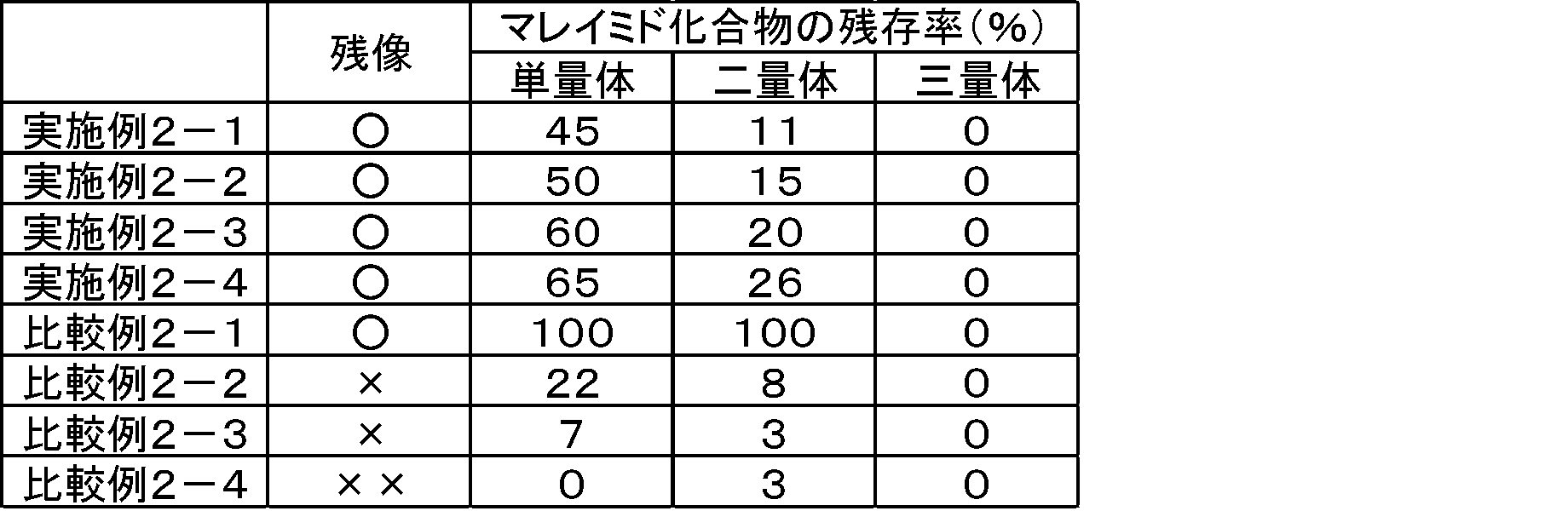
実施例2-1~2-4では、残像レベルが良かった。更に、実施例2-1~2-4では、マレイミド化合物の残存率が比較例2-1よりも全体的に低く、特に、二量体が充分に除去されていた。なお、本評価では、試料の抽出ばらつきの可能性もあって、上述した評価1と異なり、マレイミド化合物の三量体が検出されなかったが、単量体及び二量体の残存率により充分に評価できた。以上より、実施例2-1~2-4では、異方性の低下を抑制しつつ、輝点の発生を抑制する液晶表示装置の製造方法が実現されることが分かった。
比較例2-1では、実施例2-1~2-4と同様に残像レベルが良かったものの、光配向膜の洗浄を行わなかったため、マレイミド化合物の残存率が実施例2-1~2-4よりも全体的に高かった。
比較例2-2~2-4では、マレイミド化合物の残存率が実施例2-1~2-4よりも全体的に低かったものの、洗浄時に用いられたオゾン水の濃度が5ppmよりも高かった、及び/又は、オゾン水による洗浄時間が1分間よりも長かったため、残像レベルが実施例2-1~2-4よりも悪かった。
上述した評価1、2において、光配向膜の形成(偏光紫外線の照射)、光配向膜の洗浄、及び、光配向膜の焼成を順に行う第一グループ(実施例1-1~1-4、及び、比較例1-2~1-6)と、光配向膜の形成(偏光紫外線の照射)、光配向膜の焼成、及び、光配向膜の洗浄を順に行う第二グループ(実施例2-1~2-4、及び、比較例2-2~2-4)との間で、光配向膜の洗浄条件(オゾン水の濃度及び洗浄時間)が同じ例を互いに比較すると(例えば、比較例1-3及び比較例2-2を比較したり、比較例1-4及び比較例2-3を比較したりすると)、第一グループの残像レベルは、第二グループの残像レベルと同等以上であった。つまり、異方性の低下を抑制する観点からは、光配向膜の形成(偏光紫外線の照射)、光配向膜の洗浄、及び、光配向膜の焼成を順に行うことが好ましいことが分かった。
(実施例3-1)
実施例3-1の液晶表示装置を、実施形態3の製造方法によって製造した。
実施例3-1の液晶表示装置を、実施形態3の製造方法によって製造した。
<光配向膜材料による膜の形成>
まず、FFSモード用の薄膜トランジスタアレイ基板及びカラーフィルタ基板の表面上に、光配向膜材料Aをフレキソ印刷法により塗布した。その後、光配向膜材料Aに対して、仮焼成を80℃で2分間行い、続いて、本焼成を230℃で30分間行った。その結果、光配向膜材料A中のポリアミック酸P1、P2、P3のイミド化反応が進行し、光配向膜材料Aによる膜(厚み:100nm)が形成された。
まず、FFSモード用の薄膜トランジスタアレイ基板及びカラーフィルタ基板の表面上に、光配向膜材料Aをフレキソ印刷法により塗布した。その後、光配向膜材料Aに対して、仮焼成を80℃で2分間行い、続いて、本焼成を230℃で30分間行った。その結果、光配向膜材料A中のポリアミック酸P1、P2、P3のイミド化反応が進行し、光配向膜材料Aによる膜(厚み:100nm)が形成された。
<光配向膜の形成>
次に、光配向膜材料Aによる膜に対して、ワイヤーグリッド偏光板を通した偏光紫外線(波長:240~400nm、照射量:1J/cm2)を照射し、光配向膜を形成した。この際、マレイミド化合物も分解物として生成された。
次に、光配向膜材料Aによる膜に対して、ワイヤーグリッド偏光板を通した偏光紫外線(波長:240~400nm、照射量:1J/cm2)を照射し、光配向膜を形成した。この際、マレイミド化合物も分解物として生成された。
<光配向膜の洗浄>
次に、光配向膜に対して、アルカリ還元水による洗浄を1分間行った。具体的には、まず、アンモニア及び水素ガスを水に通して、pH9.4~9.5のアルカリ還元水を調製した。アルカリ還元水中のアンモニアの濃度は1mg/Lであり、水素の濃度は1.4ppmであった。そして、光配向膜が形成された2枚の基板を、ビーカーに入れたアルカリ還元水中に1分間浸漬した後、引き上げた。続いて、引き上げられた2枚の基板を、純水で1分間洗浄(リンス)した後、クリーンドライエアー(CDA)を吹き付けて乾燥させた。
次に、光配向膜に対して、アルカリ還元水による洗浄を1分間行った。具体的には、まず、アンモニア及び水素ガスを水に通して、pH9.4~9.5のアルカリ還元水を調製した。アルカリ還元水中のアンモニアの濃度は1mg/Lであり、水素の濃度は1.4ppmであった。そして、光配向膜が形成された2枚の基板を、ビーカーに入れたアルカリ還元水中に1分間浸漬した後、引き上げた。続いて、引き上げられた2枚の基板を、純水で1分間洗浄(リンス)した後、クリーンドライエアー(CDA)を吹き付けて乾燥させた。
<光配向膜の焼成>
次に、光配向膜に対して、焼成を230℃で30分間行った。
次に、光配向膜に対して、焼成を230℃で30分間行った。
<液晶表示装置の完成>
次に、光配向膜が形成された2枚の基板のうち、カラーフィルタ基板の表面上にシール材を塗布し、薄膜トランジスタアレイ基板の表面上に液晶材料を滴下した。そして、2枚の基板をシール材によって貼り合わせて液晶層を形成した後、シール材を硬化させた。その結果、実施例3-1の液晶表示装置(FFSモードの液晶表示装置)が完成した。
次に、光配向膜が形成された2枚の基板のうち、カラーフィルタ基板の表面上にシール材を塗布し、薄膜トランジスタアレイ基板の表面上に液晶材料を滴下した。そして、2枚の基板をシール材によって貼り合わせて液晶層を形成した後、シール材を硬化させた。その結果、実施例3-1の液晶表示装置(FFSモードの液晶表示装置)が完成した。
(実施例3-2)
光配向膜の洗浄を、アルカリ還元水で2分間行ったこと以外、実施例3-1と同様にして、実施例3-2の液晶表示装置を製造した。
光配向膜の洗浄を、アルカリ還元水で2分間行ったこと以外、実施例3-1と同様にして、実施例3-2の液晶表示装置を製造した。
(実施例3-3)
光配向膜の洗浄を、アルカリ還元水で3分間行ったこと以外、実施例3-1と同様にして、実施例3-3の液晶表示装置を製造した。
光配向膜の洗浄を、アルカリ還元水で3分間行ったこと以外、実施例3-1と同様にして、実施例3-3の液晶表示装置を製造した。
(比較例3-1)
光配向膜の洗浄を行わなかったこと以外、実施例3-1と同様にして、比較例3-1の液晶表示装置を製造した。比較例3-1は、比較例1-1と実質的に同様である。
光配向膜の洗浄を行わなかったこと以外、実施例3-1と同様にして、比較例3-1の液晶表示装置を製造した。比較例3-1は、比較例1-1と実質的に同様である。
[評価3]
実施例3-1~3-3、及び、比較例3-1の液晶表示装置について、以下の評価を行った。
実施例3-1~3-3、及び、比較例3-1の液晶表示装置について、以下の評価を行った。
<残像>
上述した評価1と同様な方法で、残像を評価した。結果を表3に示す。
上述した評価1と同様な方法で、残像を評価した。結果を表3に示す。
<マレイミド化合物の残存率>
まず、各例の液晶表示装置を製造する過程において、実施例3-1~3-3では光配向膜の洗浄直後の状態に対して、比較例3-1では光配向膜の形成直後(偏光紫外線の照射直後)の状態に対して、アセトニトリル及びメタノールの混合液を用いて、光配向膜の表面から試料を抽出した。その後、抽出された試料に対して液体クロマトグラフィー質量分析(LC-MS)を行い、マレイミド化合物の残存量を、単量体、二量体、及び、三量体に分類して測定した。そして、マレイミド化合物の残存量の測定値を用いて、比較例3-1におけるマレイミド化合物の残存率を100%とする規格化を行い、各例におけるマレイミド化合物の残存率を算出した。結果を表3に示す。
まず、各例の液晶表示装置を製造する過程において、実施例3-1~3-3では光配向膜の洗浄直後の状態に対して、比較例3-1では光配向膜の形成直後(偏光紫外線の照射直後)の状態に対して、アセトニトリル及びメタノールの混合液を用いて、光配向膜の表面から試料を抽出した。その後、抽出された試料に対して液体クロマトグラフィー質量分析(LC-MS)を行い、マレイミド化合物の残存量を、単量体、二量体、及び、三量体に分類して測定した。そして、マレイミド化合物の残存量の測定値を用いて、比較例3-1におけるマレイミド化合物の残存率を100%とする規格化を行い、各例におけるマレイミド化合物の残存率を算出した。結果を表3に示す。

実施例3-1~3-3では、残像レベルが非常に良かった。更に、実施例3-1~3-3では、マレイミド化合物の残存率が比較例3-1よりも全体的に低かった。以上より、実施例3-1~3-3では、異方性の低下を抑制しつつ、輝点の発生を抑制する液晶表示装置の製造方法が実現されることが分かった。
比較例3-1では、実施例3-1~3-3よりも残像レベルが悪く、更に、光配向膜の洗浄を行わなかったため、マレイミド化合物の残存率が実施例3-1~3-3よりも全体的に高かった。
(実施例4-1)
実施例4-1の液晶表示装置を、実施形態4の製造方法によって製造した。
実施例4-1の液晶表示装置を、実施形態4の製造方法によって製造した。
<光配向膜材料による膜の形成>
まず、FFSモード用の薄膜トランジスタアレイ基板及びカラーフィルタ基板の表面上に、光配向膜材料Aをフレキソ印刷法により塗布した。その後、光配向膜材料Aに対して、仮焼成を80℃で2分間行い、続いて、本焼成を230℃で30分間行った。その結果、光配向膜材料A中のポリアミック酸P1、P2、P3のイミド化反応が進行し、光配向膜材料Aによる膜(厚み:100nm)が形成された。
まず、FFSモード用の薄膜トランジスタアレイ基板及びカラーフィルタ基板の表面上に、光配向膜材料Aをフレキソ印刷法により塗布した。その後、光配向膜材料Aに対して、仮焼成を80℃で2分間行い、続いて、本焼成を230℃で30分間行った。その結果、光配向膜材料A中のポリアミック酸P1、P2、P3のイミド化反応が進行し、光配向膜材料Aによる膜(厚み:100nm)が形成された。
<光配向膜の形成>
次に、光配向膜材料Aによる膜に対して、ワイヤーグリッド偏光板を通した偏光紫外線(波長:240~400nm、照射量:1J/cm2)を照射し、光配向膜を形成した。この際、マレイミド化合物も分解物として生成された。
次に、光配向膜材料Aによる膜に対して、ワイヤーグリッド偏光板を通した偏光紫外線(波長:240~400nm、照射量:1J/cm2)を照射し、光配向膜を形成した。この際、マレイミド化合物も分解物として生成された。
<光配向膜の焼成>
次に、光配向膜に対して、焼成を230℃で30分間行った。
次に、光配向膜に対して、焼成を230℃で30分間行った。
<光配向膜の洗浄>
次に、光配向膜に対して、アルカリ還元水による洗浄を1分間行った。具体的には、まず、アンモニア及び水素ガスを水に通して、pH9.4~9.5のアルカリ還元水を調製した。アルカリ還元水中のアンモニアの濃度は1mg/Lであり、水素の濃度は1.4ppmであった。そして、光配向膜が形成された2枚の基板を、ビーカーに入れたアルカリ還元水中に1分間浸漬した後、引き上げた。続いて、引き上げられた2枚の基板を、純水で1分間洗浄(リンス)した後、クリーンドライエアー(CDA)を吹き付けて乾燥させた。
次に、光配向膜に対して、アルカリ還元水による洗浄を1分間行った。具体的には、まず、アンモニア及び水素ガスを水に通して、pH9.4~9.5のアルカリ還元水を調製した。アルカリ還元水中のアンモニアの濃度は1mg/Lであり、水素の濃度は1.4ppmであった。そして、光配向膜が形成された2枚の基板を、ビーカーに入れたアルカリ還元水中に1分間浸漬した後、引き上げた。続いて、引き上げられた2枚の基板を、純水で1分間洗浄(リンス)した後、クリーンドライエアー(CDA)を吹き付けて乾燥させた。
<液晶表示装置の完成>
次に、光配向膜が形成された2枚の基板のうち、カラーフィルタ基板の表面上にシール材を塗布し、薄膜トランジスタアレイ基板の表面上に液晶材料を滴下した。そして、2枚の基板をシール材によって貼り合わせて液晶層を形成した後、シール材を硬化させた。その結果、実施例4-1の液晶表示装置(FFSモードの液晶表示装置)が完成した。
次に、光配向膜が形成された2枚の基板のうち、カラーフィルタ基板の表面上にシール材を塗布し、薄膜トランジスタアレイ基板の表面上に液晶材料を滴下した。そして、2枚の基板をシール材によって貼り合わせて液晶層を形成した後、シール材を硬化させた。その結果、実施例4-1の液晶表示装置(FFSモードの液晶表示装置)が完成した。
(実施例4-2)
光配向膜の洗浄を、アルカリ還元水で2分間行ったこと以外、実施例4-1と同様にして、実施例4-2の液晶表示装置を製造した。
光配向膜の洗浄を、アルカリ還元水で2分間行ったこと以外、実施例4-1と同様にして、実施例4-2の液晶表示装置を製造した。
(実施例4-3)
光配向膜の洗浄を、アルカリ還元水で3分間行ったこと以外、実施例4-1と同様にして、実施例4-3の液晶表示装置を製造した。
光配向膜の洗浄を、アルカリ還元水で3分間行ったこと以外、実施例4-1と同様にして、実施例4-3の液晶表示装置を製造した。
(比較例4-1)
光配向膜の洗浄を行わなかったこと以外、実施例4-1と同様にして、比較例4-1の液晶表示装置を製造した。比較例4-1は、比較例1-1と実質的に同様である。
光配向膜の洗浄を行わなかったこと以外、実施例4-1と同様にして、比較例4-1の液晶表示装置を製造した。比較例4-1は、比較例1-1と実質的に同様である。
[評価4]
実施例4-1~4-3、及び、比較例4-1の液晶表示装置について、以下の評価を行った。
実施例4-1~4-3、及び、比較例4-1の液晶表示装置について、以下の評価を行った。
<残像>
上述した評価1と同様な方法で、残像を評価した。結果を表4に示す。
上述した評価1と同様な方法で、残像を評価した。結果を表4に示す。
<マレイミド化合物の残存率>
まず、各例の液晶表示装置を製造する過程において、実施例4-1~4-3では光配向膜の洗浄直後の状態に対して、比較例4-1では光配向膜の形成直後(偏光紫外線の照射直後)の状態に対して、アセトニトリル及びメタノールの混合液を用いて、光配向膜の表面から試料を抽出した。その後、抽出された試料に対して液体クロマトグラフィー質量分析(LC-MS)を行い、マレイミド化合物の残存量を、単量体、二量体、及び、三量体に分類して測定した。そして、マレイミド化合物の残存量の測定値を用いて、比較例4-1におけるマレイミド化合物の残存率を100%とする規格化を行い、各例におけるマレイミド化合物の残存率を算出した。結果を表4に示す。
まず、各例の液晶表示装置を製造する過程において、実施例4-1~4-3では光配向膜の洗浄直後の状態に対して、比較例4-1では光配向膜の形成直後(偏光紫外線の照射直後)の状態に対して、アセトニトリル及びメタノールの混合液を用いて、光配向膜の表面から試料を抽出した。その後、抽出された試料に対して液体クロマトグラフィー質量分析(LC-MS)を行い、マレイミド化合物の残存量を、単量体、二量体、及び、三量体に分類して測定した。そして、マレイミド化合物の残存量の測定値を用いて、比較例4-1におけるマレイミド化合物の残存率を100%とする規格化を行い、各例におけるマレイミド化合物の残存率を算出した。結果を表4に示す。

実施例4-1~4-3では、残像レベルが良かった。更に、実施例4-1~4-3では、マレイミド化合物の残存率が比較例4-1よりも全体的に低かった。なお、本評価では、試料の抽出ばらつきの可能性もあって、上述した評価3と異なり、マレイミド化合物の三量体が検出されなかったが、単量体及び二量体の残存率により充分に評価できた。以上より、実施例4-1~4-3では、異方性の低下を抑制しつつ、輝点の発生を抑制する液晶表示装置の製造方法が実現されることが分かった。
比較例4-1では、実施例4-1~4-3と同様に残像レベルが良かったものの、光配向膜の洗浄を行わなかったため、マレイミド化合物の残存率が実施例4-1~4-3よりも全体的に高かった。
上述した評価3、4において、光配向膜の形成(偏光紫外線の照射)、光配向膜の洗浄、及び、光配向膜の焼成を順に行う第三グループ(実施例3-1~3-3)と、光配向膜の形成(偏光紫外線の照射)、光配向膜の焼成、及び、光配向膜の洗浄を順に行う第四グループ(実施例4-1~4-3)との間で、光配向膜の洗浄条件(アルカリ還元水による洗浄時間)が同じ例を互いに比較すると(例えば、実施例3-1及び実施例4-1を比較したり、実施例3-2及び実施例4-2を比較したり、実施例3-3及び実施例4-3を比較したりすると)、第三グループの残像レベルは、第四グループの残像レベルよりも良かった。つまり、異方性の低下を抑制する観点からは、光配向膜の形成(偏光紫外線の照射)、光配向膜の洗浄、及び、光配向膜の焼成を順に行うことが好ましいことが分かった。光配向膜の形成後(偏光紫外線の照射後)かつ光配向膜の焼成前に、アルカリ還元水による光配向膜の洗浄を行うと、光配向膜の表面へのダメージを極力抑えつつ、マレイミド化合物を効率的に除去することができたため、光配向膜の配向規制力が向上し、残像レベルが良化したと考えられる。更に、光配向膜の洗浄後に焼成を行うことによって、光配向膜の配向規制力が更に向上し、結果的に、残像レベルが更に良化したと考えられる。
[付記]
本発明の一態様は、一対の基板と、上記一対の基板間に挟持される液晶層とを備える液晶表示装置の製造方法であって、上記一対の基板の少なくとも一方の表面上に、シクロブタン骨格を有するカルボン酸二無水物とジアミンとの重合体を含有する光配向膜材料による膜を形成する工程(1)と、上記膜に対して偏光照射を行い、光配向膜を形成する工程(2)と、上記光配向膜に対して、濃度5ppm以下のオゾン水による洗浄を1分間以下行う工程(3)とを含む液晶表示装置の製造方法(本発明の第一の液晶表示装置の製造方法)であってもよい。本態様によれば、異方性の低下を抑制しつつ、輝点の発生を抑制する液晶表示装置の製造方法が実現される。
本発明の一態様は、一対の基板と、上記一対の基板間に挟持される液晶層とを備える液晶表示装置の製造方法であって、上記一対の基板の少なくとも一方の表面上に、シクロブタン骨格を有するカルボン酸二無水物とジアミンとの重合体を含有する光配向膜材料による膜を形成する工程(1)と、上記膜に対して偏光照射を行い、光配向膜を形成する工程(2)と、上記光配向膜に対して、濃度5ppm以下のオゾン水による洗浄を1分間以下行う工程(3)とを含む液晶表示装置の製造方法(本発明の第一の液晶表示装置の製造方法)であってもよい。本態様によれば、異方性の低下を抑制しつつ、輝点の発生を抑制する液晶表示装置の製造方法が実現される。
本発明の一態様において、上記液晶表示装置の製造方法は、上記工程(3)の後に、上記光配向膜に対して焼成を行う工程(4)を更に含んでいてもよい。このような構成によれば、上記工程(3)の後にマレイミド化合物が残存しても、上記工程(4)によってマレイミド化合物が昇華され、その残存量を更に減らすことができる。
本発明の一態様において、上記液晶表示装置の製造方法は、上記工程(2)と上記工程(3)との間に、上記光配向膜に対して焼成を行う工程(4)を更に含んでいてもよい。このような構成によれば、上記工程(4)によってマレイミド化合物が昇華され、上記工程(3)を行う前にマレイミド化合物の残存量を減らすことができる。
本発明の別の一態様は、一対の基板と、上記一対の基板間に挟持される液晶層とを備える液晶表示装置の製造方法であって、上記一対の基板の少なくとも一方の表面上に、シクロブタン骨格を有するカルボン酸二無水物とジアミンとの重合体を含有する光配向膜材料による膜を形成する工程(1)と、上記膜に対して偏光照射を行い、光配向膜を形成する工程(2)と、上記光配向膜に対して、アルカリ還元水による洗浄を行う工程(3)とを含む液晶表示装置の製造方法(本発明の第二の液晶表示装置の製造方法)であってもよい。本態様によれば、異方性の低下を抑制しつつ、輝点の発生を抑制する液晶表示装置の製造方法が実現される。
本発明の別の一態様において、上記液晶表示装置の製造方法は、上記工程(3)の後に、上記光配向膜に対して焼成を行う工程(4)を更に含んでいてもよい。このような構成によれば、上記工程(3)の後にマレイミド化合物が残存しても、上記工程(4)によってマレイミド化合物が昇華され、その残存量を更に減らすことができる。
本発明の別の一態様において、上記液晶表示装置の製造方法は、上記工程(2)と上記工程(3)との間に、上記光配向膜に対して焼成を行う工程(4)を更に含んでいてもよい。このような構成によれば、上記工程(4)によってマレイミド化合物が昇華され、上記工程(3)を行う前にマレイミド化合物の残存量を減らすことができる。
本発明の一態様及び別の一態様において、上記液晶表示装置の表示モードは、IPSモード又はFFSモードであってもよい。このような構成によれば、異方性の低下を抑制しつつ、輝点の発生を抑制する、IPSモード又はFFSモードの液晶表示装置の製造方法が実現される。
Claims (7)
- 一対の基板と、前記一対の基板間に挟持される液晶層とを備える液晶表示装置の製造方法であって、
前記一対の基板の少なくとも一方の表面上に、シクロブタン骨格を有するカルボン酸二無水物とジアミンとの重合体を含有する光配向膜材料による膜を形成する工程(1)と、
前記膜に対して偏光照射を行い、光配向膜を形成する工程(2)と、
前記光配向膜に対して、濃度5ppm以下のオゾン水による洗浄を1分間以下行う工程(3)とを含むことを特徴とする液晶表示装置の製造方法。 - 前記工程(3)の後に、前記光配向膜に対して焼成を行う工程(4)を更に含むことを特徴とする請求項1に記載の液晶表示装置の製造方法。
- 前記工程(2)と前記工程(3)との間に、前記光配向膜に対して焼成を行う工程(4)を更に含むことを特徴とする請求項1に記載の液晶表示装置の製造方法。
- 一対の基板と、前記一対の基板間に挟持される液晶層とを備える液晶表示装置の製造方法であって、
前記一対の基板の少なくとも一方の表面上に、シクロブタン骨格を有するカルボン酸二無水物とジアミンとの重合体を含有する光配向膜材料による膜を形成する工程(1)と、
前記膜に対して偏光照射を行い、光配向膜を形成する工程(2)と、
前記光配向膜に対して、アルカリ還元水による洗浄を行う工程(3)とを含むことを特徴とする液晶表示装置の製造方法。 - 前記工程(3)の後に、前記光配向膜に対して焼成を行う工程(4)を更に含むことを特徴とする請求項4に記載の液晶表示装置の製造方法。
- 前記工程(2)と前記工程(3)との間に、前記光配向膜に対して焼成を行う工程(4)を更に含むことを特徴とする請求項4に記載の液晶表示装置の製造方法。
- 前記液晶表示装置の表示モードは、IPSモード又はFFSモードであることを特徴とする請求項1~6のいずれかに記載の液晶表示装置の製造方法。
Applications Claiming Priority (2)
| Application Number | Priority Date | Filing Date | Title |
|---|---|---|---|
| JP2017149266 | 2017-08-01 | ||
| JP2017-149266 | 2017-08-01 |
Publications (1)
| Publication Number | Publication Date |
|---|---|
| WO2019026705A1 true WO2019026705A1 (ja) | 2019-02-07 |
Family
ID=65232624
Family Applications (1)
| Application Number | Title | Priority Date | Filing Date |
|---|---|---|---|
| PCT/JP2018/027791 Ceased WO2019026705A1 (ja) | 2017-08-01 | 2018-07-25 | 液晶表示装置の製造方法 |
Country Status (1)
| Country | Link |
|---|---|
| WO (1) | WO2019026705A1 (ja) |
Citations (4)
| Publication number | Priority date | Publication date | Assignee | Title |
|---|---|---|---|---|
| JP2014228841A (ja) * | 2013-05-27 | 2014-12-08 | 株式会社ジャパンディスプレイ | 液晶表示装置およびその製造方法 |
| WO2015064630A1 (ja) * | 2013-10-30 | 2015-05-07 | Dic株式会社 | 液晶表示素子 |
| JP2015148747A (ja) * | 2014-02-07 | 2015-08-20 | 株式会社ジャパンディスプレイ | 液晶表示装置の製造方法および製造装置 |
| WO2017119461A1 (ja) * | 2016-01-07 | 2017-07-13 | 日産化学工業株式会社 | 液晶配向剤、液晶配向膜及びそれを用いた液晶表示素子 |
-
2018
- 2018-07-25 WO PCT/JP2018/027791 patent/WO2019026705A1/ja not_active Ceased
Patent Citations (4)
| Publication number | Priority date | Publication date | Assignee | Title |
|---|---|---|---|---|
| JP2014228841A (ja) * | 2013-05-27 | 2014-12-08 | 株式会社ジャパンディスプレイ | 液晶表示装置およびその製造方法 |
| WO2015064630A1 (ja) * | 2013-10-30 | 2015-05-07 | Dic株式会社 | 液晶表示素子 |
| JP2015148747A (ja) * | 2014-02-07 | 2015-08-20 | 株式会社ジャパンディスプレイ | 液晶表示装置の製造方法および製造装置 |
| WO2017119461A1 (ja) * | 2016-01-07 | 2017-07-13 | 日産化学工業株式会社 | 液晶配向剤、液晶配向膜及びそれを用いた液晶表示素子 |
Similar Documents
| Publication | Publication Date | Title |
|---|---|---|
| US11681184B2 (en) | Liquid crystal display device and manufacturing method thereof | |
| JP5461372B2 (ja) | 配向膜形成用溶媒、それを用いた配向膜材料および液晶表示装置の製造方法 | |
| JP5469540B2 (ja) | 液晶表示装置 | |
| TWI540368B (zh) | 液晶顯示裝置及其製造方法 | |
| JP5894567B2 (ja) | 液晶表示装置の製造方法 | |
| KR20080065543A (ko) | 신규한 폴리이미드 공중합체, 이를 포함하는 액정 배향막,및 이를 포함하는 액정 디스플레이 | |
| CN108700777A (zh) | 液晶取向剂、液晶取向膜和液晶表示元件 | |
| US10578926B2 (en) | Alignment film material and preparation method thereof, alignment film, display substrate and preparation method thereof, and liquid crystal display device | |
| TWI627202B (zh) | Composition, liquid crystal alignment treatment agent, liquid crystal alignment film, and liquid crystal display element | |
| TWI816939B (zh) | 液晶配向劑、液晶配向膜及液晶顯示元件 | |
| TWI663455B (zh) | 用於液晶配向層的洗淨組成物、使用其製備液晶配向層的方法以及包含液晶配向層的液晶顯示裝置 | |
| KR20190091551A (ko) | 액정 배향막의 제조 방법, 액정 배향막, 및 액정 표시 소자 | |
| KR20070073623A (ko) | 액정 배향용 조성물, 이로 제조된 액정 배향막, 및 이를포함하는 액정 디스플레이 | |
| JP5368250B2 (ja) | 液晶表示装置 | |
| WO2017155023A1 (ja) | 組成物、液晶パネル、液晶表示装置、電子機器 | |
| TW201421128A (zh) | 配向膜的製作方法 | |
| WO2019026705A1 (ja) | 液晶表示装置の製造方法 | |
| CN110093168B (zh) | 液晶取向剂、液晶取向膜及液晶显示装置 | |
| TWI869328B (zh) | 液晶配向劑、液晶配向膜及液晶顯示元件 | |
| TW202116872A (zh) | 液晶配向劑、液晶配向膜及使用其之液晶顯示元件 | |
| JP5639700B2 (ja) | 液晶配向剤ワニス | |
| KR20170023284A (ko) | 광배향막 리워크 방법 및 이를 포함하는 액정 표시 장치의 제조 방법 | |
| KR102712598B1 (ko) | 기판, 이를 포함하는 액정표시장치 및 그 제조방법 | |
| JP7600779B2 (ja) | 光学部材の製造方法、製造装置 | |
| CN104020612B (zh) | 配向层的形成方法和液晶面板的形成方法 |
Legal Events
| Date | Code | Title | Description |
|---|---|---|---|
| 121 | Ep: the epo has been informed by wipo that ep was designated in this application |
Ref document number: 18840946 Country of ref document: EP Kind code of ref document: A1 |
|
| NENP | Non-entry into the national phase |
Ref country code: DE |
|
| 122 | Ep: pct application non-entry in european phase |
Ref document number: 18840946 Country of ref document: EP Kind code of ref document: A1 |
|
| NENP | Non-entry into the national phase |
Ref country code: JP |