WO2019026164A1 - 電力変換装置 - Google Patents
電力変換装置 Download PDFInfo
- Publication number
- WO2019026164A1 WO2019026164A1 PCT/JP2017/027783 JP2017027783W WO2019026164A1 WO 2019026164 A1 WO2019026164 A1 WO 2019026164A1 JP 2017027783 W JP2017027783 W JP 2017027783W WO 2019026164 A1 WO2019026164 A1 WO 2019026164A1
- Authority
- WO
- WIPO (PCT)
- Prior art keywords
- electronic component
- case portion
- case
- wiring
- wiring board
- Prior art date
- Legal status (The legal status is an assumption and is not a legal conclusion. Google has not performed a legal analysis and makes no representation as to the accuracy of the status listed.)
- Ceased
Links
Images




Classifications
-
- H—ELECTRICITY
- H02—GENERATION; CONVERSION OR DISTRIBUTION OF ELECTRIC POWER
- H02M—APPARATUS FOR CONVERSION BETWEEN AC AND AC, BETWEEN AC AND DC, OR BETWEEN DC AND DC, AND FOR USE WITH MAINS OR SIMILAR POWER SUPPLY SYSTEMS; CONVERSION OF DC OR AC INPUT POWER INTO SURGE OUTPUT POWER; CONTROL OR REGULATION THEREOF
- H02M7/00—Conversion of AC power input into DC power output; Conversion of DC power input into AC power output
- H02M7/42—Conversion of DC power input into AC power output without possibility of reversal
- H02M7/44—Conversion of DC power input into AC power output without possibility of reversal by static converters
- H02M7/48—Conversion of DC power input into AC power output without possibility of reversal by static converters using discharge tubes with control electrode or semiconductor devices with control electrode
Definitions
- the present invention relates to a power converter.
- an alternating voltage is generated in an alternator connected to the engine as the engine is driven, and the generated alternating voltage is rectified by a rectifier circuit and smoothed by an electrolytic capacitor
- converts into a DC voltage by the above-mentioned method and converts the converted DC voltage into an AC voltage by an inverter (see, for example, Japanese Patent Application Laid-Open No. 2003-102200).
- the noise filter for reducing noise may be connected to the output side of an inverter according to the level of the noise of the alternating voltage converted by the inverter.
- the noise filter has large-sized winding parts as compared to the module and the rectifier circuit.
- each electronic component is resin-sealed in the state accommodated in metal storage cases, such as aluminum.
- Japanese Patent Application Laid-Open No. 2010-106698 discloses an engine generator provided with an inverter in a housing.
- a recess is partially provided in the housing, and at least a part of the air cleaner is disposed in the recess.
- JP 2010-106698 A does not mention at all the case of the inverter itself and the insulation of the electronic component with respect to the case. That is, JP 2010-106698 A does not present any effective solution to the problem that it is difficult to realize the reduction in size and weight while securing the insulation of the electronic component with respect to the storage case. .
- an object of this invention is to provide the power converter device which can implement
- a power converter is A power converter that outputs an output voltage obtained by power converting an input voltage, A storage case having a first case portion having conductivity and a second case portion having insulation; A wiring board housed in the first case portion; And an electronic component connected to the wiring of the wiring substrate and housed in the second case portion.
- the semiconductor device may further include at least one second electronic component connected to the wiring of the wiring substrate and housed in the first case portion.
- the first case portion has a first surface and a second surface opposite to the first surface, and is partially provided with a through hole penetrating from the first surface to the second surface.
- the second case portion may be joined to the first case portion so as to protrude from the second surface through the through hole.
- the second case portion is A recess is provided in a direction projecting from the second surface, and a storage portion for storing the second electronic component in the recess;
- the end portion of the recess on the first surface side may surround the storage portion, and may have an abutting portion that abuts on an inner peripheral edge of the through hole.
- the second electronic component may be disposed on the first surface.
- a plurality of the second electronic components are arranged,
- the thickness of the electronic component may be larger than at least one of the plurality of second electronic components, which is a dimension in a direction from the first surface toward the second surface.
- the electronic component and the second electronic component may further include a sealing member that seals the first surface of the storage case.
- the wiring board has a third surface opposite to the first surface of the storage case and a fourth surface opposite to the third surface.
- the power converter further includes a control unit disposed on the fourth surface of the wiring substrate and controlling an operation of the second electronic component.
- the sealing member seals the electronic component and the second electronic component on the first surface of the storage case, and the control on the fourth surface of the wiring substrate and the wiring substrate The part may be sealed.
- the second case portion may contain a resin.
- It may further have a radiation fin arranged on the 2nd field of the 1st case part.
- a plurality of the second electronic components are arranged, and the plurality of second electronic components are A rectifier circuit controlled by the control unit to rectify and output the input voltage; A module that is controlled by the control unit and converts and outputs a voltage rectified by the rectification circuit; And the reactor which adjusts and outputs the voltage which the said module output.
- the electronic component includes a winding component of a noise filter that filters and outputs a voltage output from an LC filter including the reactor, and the winding component is disposed on the third surface of the wiring substrate It is also good.
- connection portion In the power converter, It is disposed on the fourth surface of the wiring board, is connected to the input of the rectification circuit through the wiring of the wiring board, the connection portion with the wiring board is sealed by the sealing member, and the input voltage
- a smoothing capacitor that smoothes the voltage output by the The connection portion is disposed on the fourth surface of the wiring substrate, connected to the wiring substrate, the sealing member seals the connection portion with the wiring substrate, and the voltage supplied from the noise filter is used as the output voltage. And an output terminal for outputting.
- a power conversion device is a power conversion device that outputs an output voltage obtained by power conversion of an input voltage, and is a storage including a first case portion having conductivity and a second case portion having insulation.
- the electronic component connected to the wiring board in the first case portion is accommodated in the insulating second case portion, thereby making it possible to form a large storage case.
- the insulation between the electronic component and the storage case can be secured. As a result, the size and weight can be reduced while securing the insulation of the electronic component with respect to the storage case.
- FIG. 1 is a diagram illustrating an example of a configuration of a power generation system 1000 to which the power conversion device 100 according to the first embodiment is applied.
- FIG. 2 is a block diagram showing an example of the main configuration of the power conversion device 100 according to the first embodiment shown in FIG.
- FIG. 3 is a plan view showing an example of the external appearance of the power conversion device 100 shown in FIG.
- FIG. 4 is a cross-sectional view taken along line IV-IV of FIG. 3, showing an example of the configuration of power conversion device 100 shown in FIG.
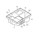
- FIG. 5 is a perspective view of the first case portion H1 of the power conversion device 100 shown in FIG.
- FIG. 6 is a plan view of second electronic components Y, M, and R on the first case portion H1 and the first case portion H1 of the power conversion device 100 shown in FIG.
- FIG. 7 is a perspective view showing a winding component W mounted on the wiring board 10 of the power conversion device 100 shown in FIG.
- FIG. 8 is an exploded perspective view of power converter 100 shown in FIG.
- FIG. 1 is a diagram illustrating an example of a configuration of a power generation system 1000 to which the power conversion device 100 according to the first embodiment is applied.
- FIG. 2 is a block diagram showing an example of the main configuration of the power conversion device 100 according to the first embodiment shown in FIG.
- FIG. 3 is a plan view showing an example of the external appearance of the power conversion device 100 shown in FIG.
- FIG. 4 is a cross-sectional view taken along line IV-IV of FIG. 3, showing an example of the configuration of power conversion device 100 shown in FIG.
- FIG. 5 is a perspective view of the first case portion H1 of the power conversion device 100 shown in FIG.
- FIG. 6 is a plan view of second electronic components Y, M, and R on the first case portion H1 and the first case portion H1 of the power conversion device 100 shown in FIG.
- FIG. 7 is a perspective view showing a winding component W mounted on the wiring board 10 of the power conversion device 100 shown in FIG.
- FIG. 8 is an exploded perspective view of power converter 100 shown in FIG.
- the power generation system 1000 is, for example, as shown in FIG. 1, an engine E, a fan X driven by an alternator (not shown) connected to the engine E, and an engine E connected to the engine E. And a power converter 100 for outputting an AC voltage (output voltage) obtained by power-converting (input voltage).
- the air flow A flows from the outside into the power generation system 1000 and is induced around the power conversion device 100 and the engine E.
- the power conversion device 100 and the engine E are cooled by the air flow A, and the heat generated by the power conversion device 100 and the engine E is released to the outside together with the air flow B.
- Such a power conversion device 100 includes, for example, a storage case H, a heat radiation fin Z, a wiring substrate 10, a sealing member 11, an input terminal TIN, and a rectifier circuit Y, as shown in FIGS. , A smoothing capacitor C, a module M, an LC filter (reactor R, first capacitor C1F) FX, a noise filter F, an output terminal TOUT, and a control unit CON.
- the storage case H has a first case portion H1 and a second case portion H2.
- the rectifier circuit Y, the module M, and the reactor R are examples of the second electronic component.
- the noise filter F includes a winding component (that is, for example, a common mode choke coil) W, which is an example of an electronic component, and a second capacitor C2F.
- the wound wire W is thicker than the at least one second electronic component (the rectifier circuit Y and the module M in the example of FIG. 3) in the direction from the first surface A1 to the second surface A2. It is an electronic component.
- Each of the capacitor C1F and the capacitor C2F may include a plurality of capacitors.
- the first case portion H1 accommodates each component of the power conversion device 100.
- the first case portion H1 has thermal conductivity from the viewpoint of dissipating the heat generated by the second electronic component (for example, the module and the rectifier circuit Y) that is a heat generation source to the outside.
- the first case portion H1 has mechanical strength from the viewpoint of stably accommodating each component of the power conversion device 100.
- the first case portion H1 is made of a metal such as aluminum so as to have both thermal conductivity and mechanical strength. Being made of metal, the first case portion H1 has conductivity.
- the first case portion H1 has a first surface A1 and a second surface A2 opposite to the first surface A1.
- the first surface A1 may be referred to as the upper surface or the inner surface
- the second surface A2 may be referred to as the lower surface or the outer surface.
- an area for arranging each of the plurality of second electronic components is provided on the first surface A1 of the first case portion H1.
- a first area for arranging the rectifier circuit Y there are a first area for arranging the rectifier circuit Y, a second area for arranging the module M, and a third area for arranging the reactor R.
- the first recess S1b which is an example of the first region
- the second recess S2b which is an example of the second region
- a third recess S3b which is an example of a third region.
- the second recess S2b is provided adjacent to the first recess S1b.
- the third recess S3b is provided adjacent to the second recess S2b.
- the area on the second surface A2 opposite to the concave portions S1b, S2b, and S3b is an area on the first surface A1 where the concave portions S1b, S2b, and S3b are not provided.
- the convex portions S1a, S2a, and S3a project more than the area on the second surface A2 located on the opposite side of the above.
- a radiation fin Z is provided so as to protrude from the second surface A2.
- the heat dissipating fins Z are cooled by the air flow A supplied from the outside, thereby releasing the heat generated by the electronic components (for example, the rectifying circuit Y and the module M) as heat sources to the outside.
- the heat dissipating fins Z may be integrally molded with the first case portion H1 by, for example, a metal casting method such as a die casting method using a metal material such as aluminum.
- the second case portion H2 houses a winding component W which is an example of the electronic component. As shown in FIG. 4, the second case portion H2 is joined to the first case portion H1 so as to protrude from the second surface A2 through the through hole 14 provided in the first case portion H1.
- the second case portion H2 has a storage portion H2a and a contact portion H2b.
- the housing portion H2a is provided with a recess H2a1 in a direction in which the second case portion H2 protrudes from the second surface A2.
- the storage portion H2a stores the winding component W in the recess H2a1.
- the contact portion H2b surrounds the storage portion H2a at the end of the recess H2a1 on the first surface A1 side and contacts the inner peripheral edge 14a of the through hole 14. By arranging the second case portion H2, the through hole 14 is closed.
- the second case portion H2 is insulated in order to ensure the insulation with the winding part W without requiring the insulation distance with the winding part W to be secured.
- the second case portion H2 may have an insulating property by being made of, for example, a resin.
- the resin forming the second case portion H2 is a resin having good followability to the sealing member 11, that is, the difference in thermal expansion coefficient with respect to the sealing member 11 is Preferably it is a small flexible resin.
- resin nylon resin etc. can be mentioned, for example.
- the wiring substrate 10 includes a plurality of wirings 10Ya, 10Ca, 10Cb, 10Ra, 10Rb, 10Fa, 10a, 10b and a plurality of electrodes 10Y, 10M, which electrically connect the terminals of the power conversion device 100 and the electronic components or electronic components. It is a substrate provided with 10R and 10F.
- the wirings and the electrodes provided on the wiring substrate 10 are expressed in a simplified manner.
- the wiring substrate 10 is disposed in the first case portion H1, and the third surface A3 opposite to the first surface A1 of the first case portion H1 and the opposite side of the third surface A3.
- the fourth surface A4 is disposed in the first case portion H1, and the third surface A3 opposite to the first surface A1 of the first case portion H1 and the opposite side of the third surface A3.
- the winding component W is housed in the second case portion H2 in a state of being electrically connected to the wiring of the wiring substrate 10 via the terminal WT of the winding component W described later and the electrode 10F.
- the input terminal TIN is disposed on the fourth surface A4 of the wiring substrate 10. As shown in FIG. 3, the input terminal TIN is connected to the input of the rectifier circuit Y via the wiring 10 Ya of the wiring substrate 10. An input voltage VIN is supplied to the input terminal TIN.
- the rectifier circuit Y which is an example of a 2nd electronic component is arrange
- the rectifier circuit Y has a plurality of terminals YT for inputting and outputting an input voltage VIN, a rectified voltage, or a control signal.
- the terminals YT are electrically connected to the electrodes 10Y of the wiring substrate 10 by a solder material or the like.
- the rectifier circuit Y is controlled by the control unit CON to rectify and output the input voltage VIN.
- the rectifying circuit Y is molded with a sealing resin different from that of the sealing member 11 to ensure insulation with the conductive first case portion H1.
- the smoothing capacitor C is disposed on the fourth surface A4 of the wiring substrate 10. As shown in FIG. 3, the smoothing capacitor C is connected to the output of the rectifier circuit Y via the wiring 10 Ca of the wiring substrate 10 and the electrode Y. The smoothing capacitor C smoothes the voltage output from the rectifier circuit Y.
- the module M which is an example of the second electronic component, is disposed adjacent to the rectifier circuit Y in the second recess S2b on the first surface A1 of the first case portion H1.
- the module M has a plurality of terminals MT for inputting and outputting a rectified voltage, an AC voltage, or a control signal. These terminals MT are electrically connected to the electrodes 10M of the wiring substrate 10 by a solder material or the like.
- the module M is connected to the output of the smoothing capacitor C via the wiring 10 ⁇ / b> Cb of the wiring substrate 10.
- the module M is controlled by the control unit CON, and converts and outputs the voltage smoothed by the smoothing capacitor C (that is, the voltage rectified by the rectification circuit Y).
- the module M is molded with a sealing resin different from the sealing member 11 to ensure insulation with the conductive first case portion H1.
- the reactor R which is an example of the second electronic component, is disposed adjacent to the module M in the third recess S3 b on the first surface A1 of the first case portion H1.
- the reactor R has a plurality of terminals RT for receiving the voltage output from the module M and outputting the adjusted voltage.
- the terminals RT are electrically connected to the electrodes 10R of the wiring substrate 10 by a solder material or the like.
- the reactor R is connected to the output of the module M via the wiring 10Ra of the wiring substrate 10 and the electrode 10M. The reactor R adjusts and outputs the voltage output from the module M.
- the output (terminal RT for output, electrode 10R) of the reactor R is connected to the noise filter F via the wiring 10Rb of the wiring substrate 10 and the first capacitor C1F disposed on the fourth surface A4 of the wiring substrate 10. Connected to the input ( Figure 3).
- the reactor R is housed in a housing having insulation, whereby insulation with the conductive first case portion H1 is secured.
- a part of the noise filter F is disposed on the third surface A3 of the wiring substrate 10, and the other part is disposed on the fourth surface A4 of the wiring substrate 10.
- the winding component W which is an example of the second electronic component, is disposed on the third surface A3 and the second capacitor C2F is disposed on the fourth surface A4. It is arranged.
- the winding component W of the noise filter F is a plurality of components for inputting and outputting a voltage between the capacitors C1F and C2F in the process of filtering the voltage output from the LC filter FX configured by the reactor R and the first capacitor C1F.
- the terminals WT are electrically connected to the electrodes 10F of the wiring substrate 10 by a solder material or the like.
- the noise filter F filters and outputs the voltage output from the LC filter FX.
- the second electronic components Y, M, R disposed on the first case portion H1 have insulation properties secured to the conductive first case portion H1 by molding in a mold or a housing. .
- the winding is exposed to the second case portion H2.
- the storage case H is formed large in order to secure the insulation distance of the second case portion H2 to the wound wire W in a state exposed to the second case portion H2.
- the insulating property of the second case part H2 with respect to the winding part W can be secured by the insulating property of the second case part H2, so that the second case part H2 can be formed large.
- the output terminal TOUT is disposed on the fourth surface A4 of the wiring substrate 10. As shown in FIG. 3, the output terminal TOUT is connected to the output of the noise filter F via the wiring 10 Fa of the wiring substrate 10. The output terminal TOUT outputs the voltage supplied from the noise filter F as an output voltage VOUT.
- the control unit CON is disposed on the fourth surface A4 of the wiring substrate 10. As shown in FIG. 3, the control unit CON controls the operation of the rectifier circuit Y by inputting and outputting a control signal to the rectifier circuit Y via the wiring 10 a and the electrode 10 Y. Further, the control unit CON controls the operation of the module M by inputting / outputting a control signal to / from the module M via the wiring 10 b and the electrode 10 M.
- the sealing member 11 seals the rectifier circuit Y, the module M, the reactor R (second electronic component) and the winding component W (electronic component) on the first surface A1 of the first case portion H1. More specifically, the sealing member 11 seals the winding component W in a state of being filled between the winding component W and the inner surface of the housing portion H2a surrounding the winding component W.
- the sealing member 11 is, for example, a sealing resin such as an epoxy resin.
- sealing member 11 seals the wiring substrate 10 and the control unit CON on the fourth surface A4 of the wiring substrate 10.
- the sealing member 11 seals a connection portion between each of the input terminal TIN, the smoothing capacitor C, the noise filter F, and the output terminal TOUT and the wiring substrate 10.
- the winding component W is connected on the third surface A3 of the wiring substrate 10. Further, on the fourth surface A4 of the wiring substrate 10, the input terminal TIN, the smoothing capacitor C, the first capacitor C1F, the second capacitor C2F, and the output terminal TOUT are connected.
- the connection of each electronic component and terminal onto the wiring substrate 10 is performed, for example, by soldering.
- the storage portion H2a of the second case portion H2 is inserted into the through hole 14 of the first case portion H1, and the inner peripheral edge 14a of the through hole 14 abuts on the second case portion H2.
- the portion H2b is abutted.
- the second case portion H2 After bringing the contact portion H2b of the second case portion H2 into contact with the inner peripheral edge 14a of the through hole 14, the second case portion H2 contacts the inner peripheral edge 14a of the through hole 14 by a fixing method such as screwing. By fixing the portion H2b, the second case portion H2 is joined to the first case portion H1. Further, as shown in FIG. 8, a rectifier circuit Y (second electronic component) is disposed in the first recess S1b, a module M (second electronic component) is disposed in the second recess S2b, and a third recess S3b Reactor R (second electronic component).
- the terminals YT, MT, RT of the electronic components Y, M, R and the electrodes 10Y, 10M, 10R of the wiring substrate 10 are electrically connected by a solder material or the like. .
- the winding component W in the second case portion H2 the electronic components Y, M, R on the first surface A1 of the first case portion H1, the wiring substrate 10, and the wiring substrate
- the sealing member 11 is formed such that the connection portion between the electronic component or the electronic component on the wiring substrate 10 and the wiring substrate 10 is sealed.
- power converter 100 shown in FIGS. 3 and 4 is obtained.
- the storage case H is secured to ensure the insulation distance between the storage case H and the electronic component whose wiring (winding) is exposed to the storage case H such as the winding component W. Case H must be made large.
- a part of the conductive storage case H is formed of the insulating second case portion H2, and in the second case portion H2, the first case portion H1 is formed.
- the winding parts W connected to the wiring of the wiring board 10 in the inside are accommodated. Thereby, the insulation of the storage case H with respect to the winding part W can be secured without requiring the storage case H to be formed large.
- the manufacturing cost of the power converter device 100 can be reduced.
- the first case portion H1 having conductivity is insulated by the simple operation of bringing the contact portion H2b of the second case portion H2 into contact with the inner peripheral edge 14a of the through hole 14.
- a second case portion H2 can be provided.
- the winding component W whose thickness is thicker than that of the second electronic component such as the rectifier circuit Y or the module M is disposed inside the second case portion H2 configured to protrude from the second surface A2. It can be stored securely.
- the power conversion device 100 is the power conversion device 100 that outputs the output voltage VOUT obtained by power conversion of the input voltage VIN, and the first case portion H1 having conductivity and the insulation Storage case H having the second case portion H2 having flexibility, the wiring board 10 stored in the first case portion H1, and the wires of the wiring board 10 connected to the wiring of the wiring case 10 and stored in the second case portion H2 And a part W.
- the insulation between the electronic component W and the storage case H is secured without requiring the storage case H to be formed large. can do.
- the size and weight can be reduced while securing the insulation of the electronic component W with respect to the storage case H.
- the rectifier circuit Y, the module M, and the reactor R are illustrated as the plurality of second electronic components.
- the second electronic component is not limited to the rectifier circuit Y, the module and the reactor R.
- the winding component W of the noise filter F is illustrated as the electronic component.
- the electronic component is not limited to the winding component W.
Landscapes
- Engineering & Computer Science (AREA)
- Power Engineering (AREA)
- Inverter Devices (AREA)
- Dc-Dc Converters (AREA)
Abstract
入力電圧を電力変換した出力電圧を出力する電力変換装置であって、導電性を有する第1ケース部および絶縁性を有する第2ケース部を有する収納ケースと、第1ケース部内に収納された配線基板と、配線基板の配線に接続され、第2ケース部内に収納された電子部品と、を備える。
Description
本発明は、電力変換装置に関する。
従来、携帯発電機等に用いられるインバータ式発電機には、エンジンの駆動にともなってエンジンに接続されたオルタネータに交流電圧を発生させ、発生した交流電圧を整流回路による整流および電解コンデンサによる平滑化によって直流電圧に変換し、変換された直流電圧をインバータで交流電圧に変換するものがある(例えば、特開2003‐102200号公報参照)。
また、インバータ式発電機においては、インバータで変換される交流電圧のノイズのレベルに応じて、インバータの出力側にノイズを低減するためのノイズフィルタを接続することがあった。ノイズフィルタは、モジュールや整流回路と比較して大型の巻線部品を有する。
このようなインバータ式発電機において、各電子部品は、アルミニウム等の金属製の収納ケースに収納された状態で樹脂封止されていた。
しかしながら、従来は、ノイズフィルタの巻線部品のような収納ケースとの絶縁距離の確保が必要な電子部品を収納するため、電子部品との距離が大きくなるように収納ケースを意図的に大きく形成しなければならなかった。したがって、従来は、収納ケースに対する電子部品の絶縁性を確保しながら小型軽量化を実現することが困難であるといった問題点があった。
なお、特開2010-106698号公報には、筐体内にインバータを備えたエンジン発電機が開示されている。このエンジン発電機では、筐体の小型化を図るために、筐体に部分的に凹部を設け、凹部にエアクリーナの少なくとも一部を配置している。しかしながら、特開2010-106698号公報は、インバータ自体の筐体および筐体に対する電子部品の絶縁性について何ら触れていない。すなわち、特開2010-106698号公報は、収納ケースに対する電子部品の絶縁性を確保しながら小型軽量化を実現することが困難であるといった問題に対して、何ら有効な解決手段を提示していない。
そこで、本発明は、収納ケースに対する電子部品の絶縁性を確保しながら小型軽量化を実現することが可能な電力変換装置を提供することを目的とする。
本発明の一態様に係る電力変換装置は、
入力電圧を電力変換した出力電圧を出力する電力変換装置であって、
導電性を有する第1ケース部および絶縁性を有する第2ケース部を有する収納ケースと、
前記第1ケース部内に収納された配線基板と、
前記配線基板の配線に接続され、前記第2ケース部内に収納された電子部品と、を備える。
入力電圧を電力変換した出力電圧を出力する電力変換装置であって、
導電性を有する第1ケース部および絶縁性を有する第2ケース部を有する収納ケースと、
前記第1ケース部内に収納された配線基板と、
前記配線基板の配線に接続され、前記第2ケース部内に収納された電子部品と、を備える。
前記電力変換装置において、
前記配線基板の配線に接続され、前記第1ケース部内に収納された少なくとも1つの第2の電子部品を更に備えてもよい。
前記配線基板の配線に接続され、前記第1ケース部内に収納された少なくとも1つの第2の電子部品を更に備えてもよい。
前記電力変換装置において、
前記第1ケース部は、第1面および前記第1面の反対側の第2面を有し、部分的に前記第1面から前記第2面まで貫通する貫通孔が設けられ、
前記第2ケース部は、前記貫通孔を通して前記第2面から突出するように前記第1ケース部に接合されていてもよい。
前記第1ケース部は、第1面および前記第1面の反対側の第2面を有し、部分的に前記第1面から前記第2面まで貫通する貫通孔が設けられ、
前記第2ケース部は、前記貫通孔を通して前記第2面から突出するように前記第1ケース部に接合されていてもよい。
前記電力変換装置において、
前記第2ケース部は、
前記第2面から突出する方向に向かって凹部が設けられ、前記凹部内に前記第2の電子部品を収納する収納部分と、
前記第1面側の前記凹部の端部において前記収納部分を囲み、前記貫通孔の内周縁に当接する当接部分と、を有してもよい。
前記第2ケース部は、
前記第2面から突出する方向に向かって凹部が設けられ、前記凹部内に前記第2の電子部品を収納する収納部分と、
前記第1面側の前記凹部の端部において前記収納部分を囲み、前記貫通孔の内周縁に当接する当接部分と、を有してもよい。
前記電力変換装置において、
前記第2の電子部品は、前記第1面上に配置されていてもよい。
前記第2の電子部品は、前記第1面上に配置されていてもよい。
前記電力変換装置において、
前記第2の電子部品は複数配置されており、
前記電子部品は、前記複数の第2の電子部品の少なくとも1つよりも前記第1面から前記第2面に向かう方向の寸法である厚みが厚くてもよい。
前記第2の電子部品は複数配置されており、
前記電子部品は、前記複数の第2の電子部品の少なくとも1つよりも前記第1面から前記第2面に向かう方向の寸法である厚みが厚くてもよい。
前記電力変換装置において、
前記収納ケースの前記第1面上で前記電子部品および前記第2の電子部品を封止する封止部材を更に備えてもよい。
前記収納ケースの前記第1面上で前記電子部品および前記第2の電子部品を封止する封止部材を更に備えてもよい。
前記電力変換装置において、
前記配線基板は、前記収納ケースの前記第1面に対向する第3面および前記第3面の反対側の第4面を有し、
前記電力変換装置は、前記配線基板の前記第4面上に配置され、前記第2の電子部品の動作を制御する制御部を更に備え、
前記封止部材は、前記収納ケースの前記第1面上で、前記電子部品および前記第2の電子部品を封止し、且つ、前記配線基板および前記配線基板の前記第4面上の前記制御部を封止してもよい。
前記配線基板は、前記収納ケースの前記第1面に対向する第3面および前記第3面の反対側の第4面を有し、
前記電力変換装置は、前記配線基板の前記第4面上に配置され、前記第2の電子部品の動作を制御する制御部を更に備え、
前記封止部材は、前記収納ケースの前記第1面上で、前記電子部品および前記第2の電子部品を封止し、且つ、前記配線基板および前記配線基板の前記第4面上の前記制御部を封止してもよい。
前記電力変換装置において、
前記第2ケース部は、樹脂を含有してもよい。
前記第2ケース部は、樹脂を含有してもよい。
前記電力変換装置において、
前記第1ケース部の前記第2面上に配置された放熱フィンを更に備えてもよい。
前記第1ケース部の前記第2面上に配置された放熱フィンを更に備えてもよい。
前記電力変換装置において、
前記第2の電子部品は複数配置されており、前記複数の第2の電子部品は、
前記制御部により制御され、前記入力電圧を整流して出力する整流回路と、
前記制御部により制御され、前記整流回路が整流した電圧を変換して出力するモジュールと、
前記モジュールが出力した電圧を調整して出力するリアクタと、を含んでもよい。
前記第2の電子部品は複数配置されており、前記複数の第2の電子部品は、
前記制御部により制御され、前記入力電圧を整流して出力する整流回路と、
前記制御部により制御され、前記整流回路が整流した電圧を変換して出力するモジュールと、
前記モジュールが出力した電圧を調整して出力するリアクタと、を含んでもよい。
前記電力変換装置において、
前記電子部品は、前記リアクタを含むLCフィルタが出力した電圧をフィルタリングして出力するノイズフィルタの巻線部品を含み、前記巻線部品は、前記配線基板の前記第3面上に配置されていてもよい。
前記電子部品は、前記リアクタを含むLCフィルタが出力した電圧をフィルタリングして出力するノイズフィルタの巻線部品を含み、前記巻線部品は、前記配線基板の前記第3面上に配置されていてもよい。
前記電力変換装置において、
前記配線基板の前記第4面上に配置され、前記配線基板の配線を介して前記整流回路の入力に接続され、前記封止部材により前記配線基板との接続部分が封止され、前記入力電圧が供給される入力端子と、
前記配線基板の前記第4面上に配置され、前記配線基板の配線を介して前記整流回路の出力に接され、前記封止部材により前記配線基板との接続部分が封止され、前記整流回路が出力した電圧を平滑化する平滑化キャパシタと、
前記配線基板の前記第4面上に配置され、前記配線基板に接続され、前記封止部材により前記配線基板との接続部分が封止され、前記ノイズフィルタから供給された電圧を前記出力電圧として出力する出力端子と、を更に備えてもよい。
前記配線基板の前記第4面上に配置され、前記配線基板の配線を介して前記整流回路の入力に接続され、前記封止部材により前記配線基板との接続部分が封止され、前記入力電圧が供給される入力端子と、
前記配線基板の前記第4面上に配置され、前記配線基板の配線を介して前記整流回路の出力に接され、前記封止部材により前記配線基板との接続部分が封止され、前記整流回路が出力した電圧を平滑化する平滑化キャパシタと、
前記配線基板の前記第4面上に配置され、前記配線基板に接続され、前記封止部材により前記配線基板との接続部分が封止され、前記ノイズフィルタから供給された電圧を前記出力電圧として出力する出力端子と、を更に備えてもよい。
本発明の一態様に係る電力変換装置は、入力電圧を電力変換した出力電圧を出力する電力変換装置であって、導電性を有する第1ケース部および絶縁性を有する第2ケース部を有する収納ケースと、前記第1ケース部内に収納された配線基板と、前記配線基板の配線に接続され、前記第2ケース部内に収納された電子部品と、を備える。
このように、本発明によれば、絶縁性を有する第2ケース部内に、第1ケース部内の配線基板に接続された電子部品を収納することで、収納ケースを大きく形成することを要することなく、電子部品と収納ケースとの絶縁性を確保することができる。
これにより、収納ケースに対する電子部品の絶縁性を確保しながら小型軽量化を実現することができる。
このように、本発明によれば、絶縁性を有する第2ケース部内に、第1ケース部内の配線基板に接続された電子部品を収納することで、収納ケースを大きく形成することを要することなく、電子部品と収納ケースとの絶縁性を確保することができる。
これにより、収納ケースに対する電子部品の絶縁性を確保しながら小型軽量化を実現することができる。
以下、図面を参照して本発明に係る実施形態を説明する。なお、以下に示す実施形態は、本発明を限定するものではない。
図1は、第1の実施形態に係る電力変換装置100が適用される発電システム1000の構成の一例を示す図である。図2は、図1に示す第1の実施形態に係る電力変換装置100の主要な構成の一例を示すブロック図である。図3は、図2に示す電力変換装置100の外観の構成の一例を示す平面図である。図4は、図3に示す電力変換装置100の構成の一例を示す図3のIV-IV断面図である。図5は、図3に示す電力変換装置100の第1ケース部H1の斜視図である。図6は、図3に示す電力変換装置100の第1ケース部H1および第1ケース部H1上の第2の電子部品Y、M、Rの平面図である。図7は、図3に示す電力変換装置100の配線基板10に搭載された巻線部品Wを示す斜視図である。図8は、図3に示す電力変換装置100の分解斜視図である。
発電システム1000は、例えば、図1に示すように、エンジンEと、エンジンEに接続されたオルタネータ(図示せず)によって駆動されるファンXと、エンジンEに接続され、オルタネータが出力した交流電圧(入力電圧)を電力変換した交流電圧(出力電圧)を出力する電力変換装置100とを備える。
この発電システム1000において、ファンXが駆動することにより、外部から気流Aが発電システム1000の内部に流れ込み、電力変換装置100及びエンジンEの周囲に誘導される。これにより、電力変換装置100及びエンジンEが気流Aにより冷却され、電力変換装置100及びエンジンEが発した熱が気流Bとともに外部に放出されることなる。
このような電力変換装置100は、例えば、図2~図4に示すように、収納ケースHと、放熱フィンZと、配線基板10と、封止部材11と、入力端子TINと、整流回路Yと、平滑化キャパシタCと、モジュールMと、LCフィルタ(リアクタR、第1のキャパシタC1F)FXと、ノイズフィルタFと、出力端子TOUTと、制御部CONと、を備える。収納ケースHは、第1ケース部H1と、第2ケース部H2とを有する。整流回路Yと、モジュールMと、リアクタRは、第2の電子部品の一例である。
図3および図4に示すように、ノイズフィルタFは、電子部品の一例である巻線部品(すなわち、例えば、コモンモードのチョークコイル)Wと、第2のキャパシタC2Fとを備える。巻線部品Wは、少なくとも1つの第2の電子部品(図3の例における整流回路YおよびモジュールM)よりも第1面A1から第2面A2に向かう方向の寸法である厚みが厚い大型の電子部品である。キャパシタC1F、キャパシタC2Fは、それぞれが複数のキャパシタを含んでいてもよい。
以下、これらの電力変換装置100の各構成部の詳細について順に説明する。
(第1ケース部H1)
第1ケース部H1は、電力変換装置100の各構成部を収納する。第1ケース部H1は、発熱源である第2の電子部品(例えば、モジュールや整流回路Y)が発する熱を外部に放熱する観点から、熱伝導性を有している。また、第1ケース部H1は、電力変換装置100の各構成部を安定的に収納する観点から、機械的強度を有している。熱伝導性および機械的強度の双方を有するように、第1ケース部H1は、アルミニウムなどの金属で構成されている。金属で構成されていることで、第1ケース部H1は、導電性を有する。
第1ケース部H1は、電力変換装置100の各構成部を収納する。第1ケース部H1は、発熱源である第2の電子部品(例えば、モジュールや整流回路Y)が発する熱を外部に放熱する観点から、熱伝導性を有している。また、第1ケース部H1は、電力変換装置100の各構成部を安定的に収納する観点から、機械的強度を有している。熱伝導性および機械的強度の双方を有するように、第1ケース部H1は、アルミニウムなどの金属で構成されている。金属で構成されていることで、第1ケース部H1は、導電性を有する。
図4および図5に示すように、第1ケース部H1は、第1面A1と、第1面A1の反対側の第2面A2とを有する。第1面A1は、上面または内面ということもでき、第2面A2は、下面または外面ということもできる。
図5に示すように、第1ケース部H1には、第2ケース部H2および巻線部品Wを配置するため、部分的に第1面A1から第2面A2まで貫通する貫通孔14が設けられている。第2ケース部H2を挿入することができるように、貫通孔14の内周は、後述する第2ケース部H2の収納部分H2aの外周よりも大きく形成されている。
図5に示すように、第1ケース部H1の第1面A1上には、複数の第2の電子部品のそれぞれを配置するための領域が設けられている。具体的には、第1面A1上には、整流回路Yを配置するための第1領域と、モジュールMを配置するための第2領域と、リアクタRを配置するための第3領域とが設けられている。より具体的には、第1面A1上には、第2面A2側に向かって凹むように、第1領域の一例である第1凹部S1bと、第2領域の一例である第2凹部S2bと、第3領域の一例である第3凹部S3bとが設けられている。第2凹部S2bは、第1凹部S1bに隣接して設けられている。また、第3凹部S3bは、第2凹部S2bに隣接して設けられている。なお、図4および図5に示すように、各凹部S1b、S2b、S3bの反対側の第2面A2上の領域は、凹部S1b、S2b、S3bが設けられていない第1面A1上の領域の反対側に位置する第2面A2上の領域よりも突出した凸部S1a、S2a、S3aとなっている。
また、第1ケース部H1には、第2面A2から突出するように放熱フィンZが設けられている。放熱フィンZは、外部から供給された気流Aにより冷却されることで、発熱源である電子部品(例えば、整流回路YおよびモジュールM)が発する熱を外部に放出する。放熱フィンZは、例えば、アルミニウム等の金属材料を用いたダイカスト法などの金属鋳造法によって、第1ケース部H1と一体成型されていてもよい。
(第2ケース部H2)
第2ケース部H2は、電子部品の一例である巻線部品Wを収納する。図4に示すように、第2ケース部H2は、第1ケース部H1に設けられた貫通孔14を通して第2面A2から突出するように第1ケース部H1に接合されている。
第2ケース部H2は、電子部品の一例である巻線部品Wを収納する。図4に示すように、第2ケース部H2は、第1ケース部H1に設けられた貫通孔14を通して第2面A2から突出するように第1ケース部H1に接合されている。
第2ケース部H2は、収納部分H2aと、当接部分H2bとを有する。収納部分H2aには、第2ケース部H2が第2面A2から突出する方向に向かって凹部H2a1が設けられている。収納部分H2aは、凹部H2a1内に巻線部品Wを収納する。
当接部分H2bは、第1面A1側の凹部H2a1の端部において収納部分H2aを囲み、貫通孔14の内周縁14aに当接する。第2ケース部H2が配置されることで、貫通孔14は塞がれた状態となる。
巻線部品Wとの絶縁距離を確保することを要することなく巻線部品Wとの絶縁性を確保するため、第2ケース部H2は、導電性を有する第1ケース部H1とは異なり、絶縁性を有している。第2ケース部H2は、例えば、樹脂で構成されていることによって絶縁性を有していてもよい。
第2ケース部H2を樹脂で構成する場合、第2ケース部H2を構成する樹脂は、封止部材11に対する追従性が良好な樹脂、すなわち、封止部材11に対して熱膨張係数の差が小さい柔軟な樹脂であることが好ましい。このような樹脂としては、例えば、ナイロン樹脂等を挙げることができる。封止部材11に対する第2ケース部H2の追従性を確保することで、封止部材11の熱膨張にともなって、封止部材11と同程度の膨張量で第2ケース部H2を熱膨張させることができる。これにより、封止部材11から第2ケース部H2に作用する熱膨張による応力を緩和することができるので、応力によって第2ケース部H2にクラック等の破損が生じてしまうことを抑制することができる。
(配線基板10)
配線基板10は、電力変換装置100の端子と電子部品あるいは電子部品同士を電気的に接続する複数の配線10Ya、10Ca、10Cb、10Ra、10Rb、10Fa、10a、10bおよび複数の電極10Y、10M、10R、10Fが設けられた基板である。なお、図3では、配線基板10に設けられた配線および電極を簡略化して表現している。図4に示すように、配線基板10は、第1ケース部H1内に配置されており、第1ケース部H1の第1面A1に対向する第3面A3と、第3面A3の反対側の第4面A4とを有する。
配線基板10は、電力変換装置100の端子と電子部品あるいは電子部品同士を電気的に接続する複数の配線10Ya、10Ca、10Cb、10Ra、10Rb、10Fa、10a、10bおよび複数の電極10Y、10M、10R、10Fが設けられた基板である。なお、図3では、配線基板10に設けられた配線および電極を簡略化して表現している。図4に示すように、配線基板10は、第1ケース部H1内に配置されており、第1ケース部H1の第1面A1に対向する第3面A3と、第3面A3の反対側の第4面A4とを有する。
巻線部品Wは、後述する巻線部品Wの端子WT、電極10Fを介して配線基板10の配線に電気的に接続された状態で第2ケース部H2内に収納されている。
(電子部品、端子)
入力端子TINは、配線基板10の第4面A4上に配置されている。図3に示すように、入力端子TINは、配線基板10の配線10Yaを介して整流回路Yの入力に接続されている。入力端子TINには、入力電圧VINが供給される。
入力端子TINは、配線基板10の第4面A4上に配置されている。図3に示すように、入力端子TINは、配線基板10の配線10Yaを介して整流回路Yの入力に接続されている。入力端子TINには、入力電圧VINが供給される。
第2の電子部品の一例である整流回路Yは、第1ケース部H1の第1面A1上の第1凹部S1bに配置されている。図6に示すように、整流回路Yは、入力電圧VIN、整流電圧、又は制御信号を入出力するための複数の端子YTを有する。これらの端子YTは、配線基板10の電極10Yにはんだ材等によって電気的に接続されている。整流回路Yは、制御部CONにより制御され、入力電圧VINを整流して出力する。整流回路Yは、封止部材11とは異なる封止樹脂によってモールドされていることで、導電性を有する第1ケース部H1との絶縁性が確保されている。
平滑化キャパシタCは、配線基板10の第4面A4上に配置されている。図3に示すように、平滑化キャパシタCは、配線基板10の配線10Caおよび電極Yを介して整流回路Yの出力に接続されている。平滑化キャパシタCは、整流回路Yが出力した電圧を平滑化する。
第2の電子部品の一例であるモジュールMは、第1ケース部H1の第1面A1上の第2凹部S2bに整流回路Yに隣接して配置されている。図6に示すように、モジュールMは、整流電圧、交流電圧、又は制御信号を入出力するための複数の端子MTを有する。これらの端子MTは、配線基板10の電極10Mにはんだ材等によって電気的に接続されている。図3に示すように、モジュールMは、配線基板10の配線10Cbを介して平滑化キャパシタCの出力に接続されている。モジュールMは、制御部CONにより制御され、平滑化キャパシタCが平滑化した電圧(すなわち、整流回路Yが整流した電圧)を変換して出力する。モジュールMは、封止部材11とは異なる封止樹脂によってモールドされていることで、導電性を有する第1ケース部H1との絶縁性が確保されている。
第2の電子部品の一例であるリアクタRは、第1ケース部H1の第1面A1上の第3凹部S3bにモジュールMに隣接して配置されている。図6に示すように、リアクタRは、モジュールMが出力した電圧が入力され、調整した電圧を出力するための複数の端子RTを有する。これらの端子RTは、配線基板10の電極10Rにはんだ材等によって電気的に接続されている。図3に示すように、リアクタRは、配線基板10の配線10Raおよび電極10Mを介してモジュールMの出力に接続されている。リアクタRは、モジュールMが出力した電圧を調整して出力する。リアクタRの出力(出力用の端子RT、電極10R)は、配線基板10の配線10Rbと配線基板10の第4面A4上に配置された第1のキャパシタC1Fとを介して、ノイズフィルタFの入力に接続されている(図3)。リアクタRは、絶縁性を有する筐体内に収容されていることで、導電性を有する第1ケース部H1との絶縁性が確保されている。
ノイズフィルタFは、一部が配線基板10の第3面A3上に配置され、他の一部が配線基板10の第4面A4上に配置されている。図3に示される例において、ノイズフィルタFのうち、第2の電子部品の一例である巻線部品Wは第3面A3上に配置され、第2のキャパシタC2Fは、第4面A4上に配置されている。ノイズフィルタFの巻線部品Wは、リアクタRおよび第1のキャパシタC1Fで構成されるLCフィルタFXが出力した電圧をフィルタリングする過程でキャパシタC1F、C2Fとの間で電圧を入出力するための複数の端子WTを有する。これらの端子WTは、配線基板10の電極10Fにはんだ材等によって電気的に接続されている。ノイズフィルタFは、LCフィルタFXが出力した電圧をフィルタリングして出力する。
第1ケース部H1上に配置される第2の電子部品Y、M、Rは、導電性を有する第1ケース部H1に対して、モールドや筐体内への収容によって絶縁性が確保されている。これに対して、巻線部品Wは、リアクタRのように筐体で覆われている構成とは異なり、第2ケース部H2に対して巻線が露出されている。もし、第2ケース部H2が導電性を有する場合、第2ケース部H2に対して露出した状態の巻線部品Wに対する第2ケース部H2の絶縁距離を確保するため、収納ケースHを大きく形成する必要がある。しかるに、本実施形態においては、第2ケース部H2が絶縁性を有することで、巻線部品Wに対する第2ケース部H2の絶縁性を確保できるので、第2ケース部H2を大きく形成することを要しない。
出力端子TOUTは、配線基板10の第4面A4上に配置されている。図3に示すように、出力端子TOUTは、配線基板10の配線10Faを介してノイズフィルタFの出力に接続されている。出力端子TOUTは、ノイズフィルタFから供給された電圧を出力電圧VOUTとして出力する。
制御部CONは、配線基板10の第4面A4上に配置されている。図3に示すように、制御部CONは、配線10aおよび電極10Yを介して整流回路Yに制御信号を入出力することで、整流回路Yの動作を制御するようになっている。また、制御部CONは、配線10bおよび電極10Mを介してモジュールMに制御信号を入出力することで、モジュールMの動作を制御するようになっている。
(封止部材11)
封止部材11は、第1ケース部H1の第1面A1上で、整流回路Y、モジュールM、リアクタR(第2の電子部品)および巻線部品W(電子部品)を封止する。より具体的には、封止部材11は、巻線部品Wと巻線部品Wを囲む収納部分H2aの内表面との間に充填された状態で、巻線部品Wを封止する。封止部材11は、例えば、エポキシ樹脂等の封止樹脂である。
封止部材11は、第1ケース部H1の第1面A1上で、整流回路Y、モジュールM、リアクタR(第2の電子部品)および巻線部品W(電子部品)を封止する。より具体的には、封止部材11は、巻線部品Wと巻線部品Wを囲む収納部分H2aの内表面との間に充填された状態で、巻線部品Wを封止する。封止部材11は、例えば、エポキシ樹脂等の封止樹脂である。
また、封止部材11は、配線基板10および配線基板10の第4面A4上の制御部CONを封止する。
また、封止部材11は、入力端子TIN、平滑化キャパシタC、ノイズフィルタFおよび出力端子TOUTのそれぞれと配線基板10との接続部分を封止する。
以下、上述した構成を有する電力変換装置100の組立方法(製造方法)の一例について説明する。
電力変換装置100の組立にあたっては、図7に示すように、配線基板10の第3面A3上に巻線部品Wを接続する。また、配線基板10の第4面A4上には、入力端子TIN、平滑化キャパシタC、第1のキャパシタC1F、第2のキャパシタC2Fおよび出力端子TOUTを接続する。配線基板10上へ各電子部品および端子の接続は、例えば、はんだ付けで行う。
そして、図8に示すように、第1ケース部H1の貫通孔14に、第2ケース部H2の収納部分H2aを挿入して、貫通孔14の内周縁14aに第2ケース部H2の当接部分H2bを当接させる。
貫通孔14の内周縁14aに第2ケース部H2の当接部分H2bを当接させた後、例えば、ねじ止め等の固定方法によって貫通孔14の内周縁14aに第2ケース部H2の当接部分H2bを固定することで、第1ケース部H1に第2ケース部H2を接合する。また、図8に示すように、第1凹部S1bに整流回路Y(第2の電子部品)を配置し、第2凹部S2bにモジュールM(第2の電子部品)を配置し、第3凹部S3bにリアクタR(第2の電子部品)を配置する。
その後、巻線部品Wが配置された配線基板10の第3面A3を第1ケース部H1の第1面A1に対向させた状態で、第1ケース部H1の第1面A1上に配線基板10を配置する。
第1面A1上に配線基板10を配置した後、電子部品Y、M、Rの端子YT、MT、RTと配線基板10の電極10Y、10M、10Rとをはんだ材等によって電気的に接続する。
その後、例えば、樹脂ポッティング等の方法で、第2ケース部H2内の巻線部品W、第1ケース部H1の第1面A1上の電子部品Y、M、R、配線基板10、および配線基板10上の電子部品または電子部品と配線基板10との接続部分が封止されるように、封止部材11を形成する。以上のようにして、図3および図4に示した電力変換装置100が得られる。
以下、本実施形態によってもたらされる作用について説明する。
収納ケースH全体が導電性を有する場合、巻線部品Wのような収納ケースHに対して配線(巻線)が露出された電子部品と、収納ケースHとの絶縁距離を確保するため、収納ケースHを大きく形成しなければならない。
これに対して、本実施形態によれば、導電性を有する収納ケースHの一部を、絶縁性を有する第2ケース部H2によって形成し、第2ケース部H2内に、第1ケース部H1内の配線基板10の配線に接続された巻線部品Wを収納する。これにより、収納ケースHを大きく形成することを要することなく、巻線部品Wに対する収納ケースHの絶縁性を確保することができる。
また、本実施形態によれば、第2ケース部H2自体の絶縁性によって巻線部品Wと第2ケース部H2との絶縁性が確保されているため、巻線部品Wと第2ケース部H2との距離を抑えることができる。これにより、巻線部品Wと第2ケース部H2との間に充填される封止部材11の使用量を抑えることができるので、電力変換装置100の製造コストを削減することができる。
また、本実施形態によれば、貫通孔14の内周縁14aに第2ケース部H2の当接部分H2bを当接させる簡便な作業によって、導電性を有する第1ケース部H1に、絶縁性を有する第2ケース部H2を設けることができる。
また、本実施形態によれば、整流回路YやモジュールMなどの第2の電子部品よりも厚みが厚い巻線部品Wを、第2面A2から突出する構成の第2ケース部H2の内部に確実に収納することができる。
以上のように、本発明の一態様に係る電力変換装置100は、入力電圧VINを電力変換した出力電圧VOUTを出力する電力変換装置100であって、導電性を有する第1ケース部H1および絶縁性を有する第2ケース部H2を有する収納ケースHと、第1ケース部H1内に収納された配線基板10と、配線基板10の配線に接続され、第2ケース部H2内に収納された電子部品Wとを備える。
このように、絶縁性を有する第2ケース部H2内に電子部品Wを収納することで、収納ケースHを大きく形成することを要することなく、電子部品Wと収納ケースHとの絶縁性を確保することができる。これにより、収納ケースHに対する電子部品Wの絶縁性を確保しながら小型軽量化を実現することができる。
なお、上述した実施形態においては、複数の第2の電子部品として、整流回路Y、モジュールMおよびリアクタRを例示した。しかしながら、第2の電子部品は、整流回路Y、モジュールおよびリアクタRに限定されるものではない。また、上述した実施形態においては、電子部品として、ノイズフィルタFの巻線部品Wを例示した。しかしながら、電子部品は、巻線部品Wに限定されるものではない。
上述した実施形態は、あくまで一例であって、発明の範囲を限定するものではない。発明の要旨を逸脱しない限度において、上述した実施形態に対して種々の変更を行うことができる。変更された実施形態は、特許請求の範囲に記載された発明とその均等の範囲に含まれるものである。
Claims (13)
- 入力電圧を電力変換した出力電圧を出力する電力変換装置であって、
導電性を有する第1ケース部および絶縁性を有する第2ケース部を有する収納ケースと、
前記第1ケース部内に収納された配線基板と、
前記配線基板の配線に接続され、前記第2ケース部内に収納された電子部品と、を備えることを特徴とする電力変換装置。 - 前記配線基板の配線に接続され、前記第1ケース部内に収納された少なくとも1つの第2の電子部品を更に備えることを特徴とする請求項1に記載の電力変換装置。
- 前記第1ケース部は、第1面および前記第1面の反対側の第2面を有し、部分的に前記第1面から前記第2面まで貫通する貫通孔が設けられ、
前記第2ケース部は、前記貫通孔を通して前記第2面から突出するように前記第1ケース部に接合されていることを特徴とする請求項2に記載の電力変換装置。 - 前記第2ケース部は、
前記第2面から突出する方向に向かって凹部が設けられ、前記凹部内に前記第2の電子部品を収納する収納部分と、
前記第1面側の前記凹部の端部において前記収納部分を囲み、前記貫通孔の内周縁に当接する当接部分と、を有することを特徴とする請求項3に記載の電力変換装置。 - 前記第2の電子部品は、前記第1面上に配置されていることを特徴とする請求項3に記載の電力変換装置。
- 前記第2の電子部品は複数配置されており、
前記電子部品は、前記複数の第2の電子部品の少なくとも1つよりも前記第1面から前記第2面に向かう方向の寸法である厚みが厚いことを特徴とする請求項3に記載の電力変換装置。 - 前記収納ケースの前記第1面上で前記電子部品および前記第2の電子部品を封止する封止部材を更に備えることを特徴とする請求項3に記載の電力変換装置。
- 前記配線基板は、前記収納ケースの前記第1面に対向する第3面および前記第3面の反対側の第4面を有し、
前記電力変換装置は、前記配線基板の前記第4面上に配置され、前記第2の電子部品の動作を制御する制御部を更に備え、
前記封止部材は、前記収納ケースの前記第1面上で、前記電子部品および前記第2の電子部品を封止し、且つ、前記配線基板および前記配線基板の前記第4面上の前記制御部を封止することを特徴とする請求項7に記載の電力変換装置。 - 前記第2ケース部は、樹脂を含有することを特徴とする請求項3に記載の電力変換装置。
- 前記第1ケース部の前記第2面上に配置された放熱フィンを更に備えることを特徴とする請求項3に記載の電力変換装置。
- 前記第2の電子部品は複数配置されており、前記複数の第2の電子部品は、
前記制御部により制御され、前記入力電圧を整流して出力する整流回路と、
前記制御部により制御され、前記整流回路が整流した電圧を変換して出力するモジュールと、
前記モジュールが出力した電圧を調整して出力するリアクタと、を含むことを特徴とする請求項8に記載の電力変換装置。 - 前記電子部品は、前記リアクタを含むLCフィルタが出力した電圧をフィルタリングして出力するノイズフィルタの巻線部品を含み、前記巻線部品は、前記配線基板の前記第3面上に配置されていることを特徴とする請求項11に記載の電力変換装置。
- 前記配線基板の前記第4面上に配置され、前記配線基板の配線を介して前記整流回路の入力に接続され、前記封止部材により前記配線基板との接続部分が封止され、前記入力電圧が供給される入力端子と、
前記配線基板の前記第4面上に配置され、前記配線基板の配線を介して前記整流回路の出力に接され、前記封止部材により前記配線基板との接続部分が封止され、前記整流回路が出力した電圧を平滑化する平滑化キャパシタと、
前記配線基板の前記第4面上に配置され、前記配線基板に接続され、前記封止部材により前記配線基板との接続部分が封止され、前記ノイズフィルタから供給された電圧を前記出力電圧として出力する出力端子と、を更に備えることを特徴とする請求項12に記載の電力変換装置。
Priority Applications (2)
| Application Number | Priority Date | Filing Date | Title |
|---|---|---|---|
| PCT/JP2017/027783 WO2019026164A1 (ja) | 2017-07-31 | 2017-07-31 | 電力変換装置 |
| JP2018526835A JP6483330B1 (ja) | 2017-07-31 | 2017-07-31 | 電力変換装置 |
Applications Claiming Priority (1)
| Application Number | Priority Date | Filing Date | Title |
|---|---|---|---|
| PCT/JP2017/027783 WO2019026164A1 (ja) | 2017-07-31 | 2017-07-31 | 電力変換装置 |
Publications (1)
| Publication Number | Publication Date |
|---|---|
| WO2019026164A1 true WO2019026164A1 (ja) | 2019-02-07 |
Family
ID=65232400
Family Applications (1)
| Application Number | Title | Priority Date | Filing Date |
|---|---|---|---|
| PCT/JP2017/027783 Ceased WO2019026164A1 (ja) | 2017-07-31 | 2017-07-31 | 電力変換装置 |
Country Status (2)
| Country | Link |
|---|---|
| JP (1) | JP6483330B1 (ja) |
| WO (1) | WO2019026164A1 (ja) |
Citations (3)
| Publication number | Priority date | Publication date | Assignee | Title |
|---|---|---|---|---|
| JP2005268491A (ja) * | 2004-03-18 | 2005-09-29 | Hoshizaki Electric Co Ltd | 電装箱 |
| WO2016047212A1 (ja) * | 2014-09-25 | 2016-03-31 | 日立オートモティブシステムズ株式会社 | 電力変換装置 |
| JP2016082626A (ja) * | 2014-10-10 | 2016-05-16 | 株式会社デンソー | 電力変換装置 |
-
2017
- 2017-07-31 JP JP2018526835A patent/JP6483330B1/ja active Active
- 2017-07-31 WO PCT/JP2017/027783 patent/WO2019026164A1/ja not_active Ceased
Patent Citations (3)
| Publication number | Priority date | Publication date | Assignee | Title |
|---|---|---|---|---|
| JP2005268491A (ja) * | 2004-03-18 | 2005-09-29 | Hoshizaki Electric Co Ltd | 電装箱 |
| WO2016047212A1 (ja) * | 2014-09-25 | 2016-03-31 | 日立オートモティブシステムズ株式会社 | 電力変換装置 |
| JP2016082626A (ja) * | 2014-10-10 | 2016-05-16 | 株式会社デンソー | 電力変換装置 |
Also Published As
| Publication number | Publication date |
|---|---|
| JPWO2019026164A1 (ja) | 2019-08-08 |
| JP6483330B1 (ja) | 2019-03-13 |
Similar Documents
| Publication | Publication Date | Title |
|---|---|---|
| JP6716025B2 (ja) | 電力変換装置用フィルタモジュール | |
| US8125304B2 (en) | Power electronic module with an improved choke and methods of making same | |
| US9776514B2 (en) | DC-DC converter | |
| JPWO2015053139A1 (ja) | 電力変換装置 | |
| JP2017212774A (ja) | 電力変換器 | |
| JP2017028747A (ja) | 電力変換装置 | |
| NL2021196B1 (en) | Module and power conversion device | |
| JP6483330B1 (ja) | 電力変換装置 | |
| CN112216484B (zh) | 线圈模块和电力转换器 | |
| JP6439483B2 (ja) | 電力変換装置 | |
| US12431768B2 (en) | Integrated motor and drive assembly | |
| JP6483331B1 (ja) | 電力変換装置 | |
| JP7053382B2 (ja) | 電力変換装置 | |
| JP6556954B2 (ja) | 電力変換装置 | |
| JP2002369528A (ja) | Dc−dcコンバータ装置 | |
| US10461659B2 (en) | Semiconductor device and power converting device | |
| JP6487119B1 (ja) | 電力変換装置 | |
| JP7051602B2 (ja) | 電力変換装置 | |
| JP6457155B1 (ja) | 電力変換装置 | |
| JP6435906B2 (ja) | 電力変換装置 | |
| JP6240516B2 (ja) | 電力変換装置 | |
| JP2025177080A (ja) | 電力変換装置 | |
| JP2019213339A (ja) | 電力変換装置 |
Legal Events
| Date | Code | Title | Description |
|---|---|---|---|
| ENP | Entry into the national phase |
Ref document number: 2018526835 Country of ref document: JP Kind code of ref document: A |
|
| 121 | Ep: the epo has been informed by wipo that ep was designated in this application |
Ref document number: 17920561 Country of ref document: EP Kind code of ref document: A1 |
|
| NENP | Non-entry into the national phase |
Ref country code: DE |
|
| 122 | Ep: pct application non-entry in european phase |
Ref document number: 17920561 Country of ref document: EP Kind code of ref document: A1 |