WO2019026161A1 - 電力変換装置 - Google Patents
電力変換装置 Download PDFInfo
- Publication number
- WO2019026161A1 WO2019026161A1 PCT/JP2017/027780 JP2017027780W WO2019026161A1 WO 2019026161 A1 WO2019026161 A1 WO 2019026161A1 JP 2017027780 W JP2017027780 W JP 2017027780W WO 2019026161 A1 WO2019026161 A1 WO 2019026161A1
- Authority
- WO
- WIPO (PCT)
- Prior art keywords
- module
- disposed
- storage case
- wiring board
- reactor
- Prior art date
- Legal status (The legal status is an assumption and is not a legal conclusion. Google has not performed a legal analysis and makes no representation as to the accuracy of the status listed.)
- Ceased
Links
Images






Classifications
-
- H—ELECTRICITY
- H02—GENERATION; CONVERSION OR DISTRIBUTION OF ELECTRIC POWER
- H02M—APPARATUS FOR CONVERSION BETWEEN AC AND AC, BETWEEN AC AND DC, OR BETWEEN DC AND DC, AND FOR USE WITH MAINS OR SIMILAR POWER SUPPLY SYSTEMS; CONVERSION OF DC OR AC INPUT POWER INTO SURGE OUTPUT POWER; CONTROL OR REGULATION THEREOF
- H02M7/00—Conversion of AC power input into DC power output; Conversion of DC power input into AC power output
- H02M7/42—Conversion of DC power input into AC power output without possibility of reversal
- H02M7/44—Conversion of DC power input into AC power output without possibility of reversal by static converters
- H02M7/48—Conversion of DC power input into AC power output without possibility of reversal by static converters using discharge tubes with control electrode or semiconductor devices with control electrode
Definitions
- the present invention relates to a power converter.
- an AC voltage is generated in an alternator by driving an engine, and the generated AC voltage is converted into a DC voltage by rectification by a rectifier circuit and smoothing by an electrolytic capacitor.
- an apparatus that converts the DC voltage into an AC voltage by an inverter (see, for example, Japanese Patent Application Laid-Open No. 2003-102200).
- a noise filter for reducing noise is connected to the output side of the inverter according to the level of the noise of the AC voltage converted by the inverter.
- the power conversion device is configured by resin sealing in a state where the electronic component is stored in the storage case.
- a rectifier circuit for rectifying an alternating voltage and an H bridge circuit for converting power are configured as one module sealed.
- a voltage obtained by rectifying an input voltage (AC voltage) from the module is output to a smoothing capacitor outside the module, and the DC voltage smoothed by the smoothing capacitor is the module. Is input to an electronic component that converts the voltage of Thereafter, the AC voltage converted by the module is output as the output voltage of the power conversion device via the reactor and the noise filter.
- AC voltage input voltage
- a power converter that outputs an output voltage obtained by power converting an input voltage
- a storage case having a first surface and a second surface opposite to the first surface
- a wiring board disposed in the storage case and having a third surface opposite to the first surface of the storage case and a fourth surface opposite to the third surface
- a rectifying module Y which is disposed in a first area on the first surface of the storage case, is electrically connected to the wiring board, and rectifies and outputs the input voltage
- An H-bridge module disposed adjacent to the rectification module in a second region on the first surface of the storage case, electrically connected to the wiring board, and converting and outputting a voltage rectified by the rectification module
- a reactor disposed adjacent to the H-bridge module in a third region on the first surface of the storage case, electrically connected to the wiring board, and adjusting and outputting a voltage output from the H-bridge module
- a control unit disposed on the fourth surface of the wiring board and controlling operations of the rectification module and
- the rectifying module has a second sealing member different from the first sealing member, and a circuit portion of the rectifying module is sealed by the second sealing member.
- the H-bridge module has a third sealing member different from the first sealing member, and a circuit portion of the H-bridge module is sealed by the third sealing member. It is characterized by
- the first direction in which the rectifying module and the H bridge module are adjacent is different from the second direction in which the H bridge module and the reactor are adjacent on the first surface of the storage case,
- the fourth surface of the wiring substrate so that the smoothing capacitor is positioned adjacent to the rectifying module and above the region adjacent to the H bridge module in the second direction on the opposite side to the reactor. It is characterized by being placed on top.
- the device may further include an input terminal to which the input voltage is supplied.
- the first sealing member is disposed on the fourth surface of the wiring substrate, connected to the wiring substrate, and a connection portion with the wiring substrate is sealed by the first sealing member, and the voltage supplied from the noise filter is It further comprises an output terminal for outputting as an output voltage.
- the amount of heat generated per unit time during operation of the rectifying module, the H bridge module, and the reactor disposed on the first surface of the storage case is disposed on the fourth surface of the wiring board It is characterized in that the amount of heat generation per unit time during operation of the smoothing capacitor and the noise filter is larger.
- the heat generation amount per unit time during the operation of the H bridge module is larger than the heat generation amount per unit time during the operation of the rectification module.
- a calorific value per unit time during operation of the reactor is smaller than a calorific value per unit time during operation of the rectifying module and the H bridge module.
- the first region of the first surface in which the rectifying module is disposed is a first recess formed to be recessed in the first surface of the storage case, and the second surface side of the first recess is And projecting from the second surface of the storage case.
- the second region of the first surface in which the H-bridge module is disposed is a second recess formed to be recessed in the first surface of the storage case, and the second surface side of the second recess is disposed. Is projecting from the second surface of the storage case.
- the third region of the first surface in which the reactor is disposed is a third recess formed to be recessed in the first surface of the storage case, and the second surface side of the third recess is: It protrudes from the said 2nd surface of the said storage case, It is characterized by the above-mentioned.
- the apparatus may further include a heat dissipating fin disposed on the second surface of the storage case.
- the heat radiation fin is housed on the second surface with respect to a region ranging from the first region where the rectification module of the first surface is disposed to the second region where the H bridge module is disposed. It is characterized by extending so as to continuously face each other through the case.
- the radiation fin is provided on the second surface so as to extend in a direction parallel to a first direction in which the first region and the second region are adjacent on the first surface. It is characterized by
- the heat dissipating fins are configured to dissipate heat generated by at least the rectifying module and the H bridge module to the outside by being cooled by an air flow supplied from the outside. At least a part of the air flow induced by the heat dissipating fins is disposed to avoid the second surface side of the third recess in which the reactor is disposed.
- a power conversion device is a power conversion device that outputs an output voltage obtained by power conversion of an input voltage, and includes a first surface and a storage case having a second surface opposite to the first surface.
- a wiring board disposed in the storage case and having a third surface facing the first surface of the storage case and a fourth surface opposite to the third surface, and the first surface of the storage case
- a rectifying module Y disposed in the first area of the storage case, electrically connected to the wiring board, and rectifying and outputting the input voltage; and the rectifying module in the second area on the first surface of the storage case.
- An H-bridge module disposed adjacent to and electrically connected to the wiring board and converting and outputting a voltage rectified by the rectifying module, and the H-bridge module in a third area on the first surface of the storage case
- a reactor electrically connected to the wiring board, and adjusting and outputting a voltage output from the H-bridge module, and a reactor disposed on the fourth surface of the wiring board, the rectification module and the H-bridge
- a control unit for controlling the operation of the module and the fourth surface of the wiring board are connected to the output of the rectification module via the wiring of the wiring board, and the voltage output from the rectification module is smoothed
- the power conversion device can reduce the size while optimizing the current path in consideration of the margin of thermal design.
- FIG. 1 is a diagram illustrating an example of a configuration of a power generation system 1000 to which the power conversion device 100 according to the first embodiment is applied.
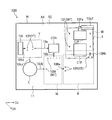
- FIG. 2 is a block diagram showing an example of the main configuration of the power conversion device 100 according to the first embodiment shown in FIG.
- FIG. 3 is a top view showing an example of the external appearance of the power conversion device 100 shown in FIG.
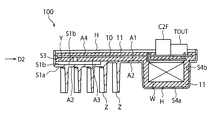
- FIG. 4 is a cross-sectional view showing an example of the configuration of power conversion device 100 shown in FIG. 3.
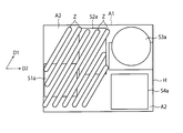
- FIG. 5 is a bottom view of the storage case H of the power conversion device 100 shown in FIG. 6 is a side view of the storage case H shown in FIG.
- FIG. 7 is a perspective view of the storage case H shown in FIG. FIG.
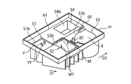
- FIG. 8 is a perspective view showing an example of the state before sealing in which the first to third electronic components Y, M, R are mounted on the storage case H shown in FIG.
- FIG. 9 is a top view showing an example of a state before resin sealing in which the first to third electronic components Y, M, R are mounted on the storage case H shown in FIG.
- FIG. 10 is a top view showing an example of the wiring board 10 shown in FIG. 3 and FIG.
- FIG. 1 is a diagram illustrating an example of a configuration of a power generation system 1000 to which the power conversion device 100 according to the first embodiment is applied.
- FIG. 2 is a block diagram showing an example of a main configuration of the power conversion device 100 according to the first embodiment shown in FIG.
- FIG. 3 is a top view which shows an example of a structure of the external appearance of the power converter device 100 shown in FIG. 4 is a cross-sectional view showing an example of the configuration of power conversion device 100 shown in FIG. 5 is a bottom view of the storage case H of the power conversion device 100 shown in FIG. 6 is a side view of the storage case H shown in FIG. 7 is a perspective view of the storage case H shown in FIG. Further, FIG.
- FIG. 8 is a perspective view showing an example of a state before sealing in which the first to third electronic components Y, M, R are mounted on the storage case H shown in FIG. 9 is a top view showing an example of the state before resin sealing, in which the first to third electronic components Y, M, R are mounted on the storage case H shown in FIG. 10 is a top view showing an example of the wiring substrate 10 shown in FIG. 3 and FIG.
- FIG. 2 shows a state in which each electronic component of the power conversion device 100 and the wiring substrate 10 are sealed by the first sealing member 11.
- FIG. 4 shows a cross section of the power conversion device 100 along a straight line parallel to the second direction D2 passing through the fourth electronic component W.
- the power generation system 1000 includes a fan X driven by an engine E and an alternator (not shown) connected to the engine E, and an AC voltage (input voltage VIN) output from the alternator. And a power converter 100 for outputting an AC voltage (output voltage VOUT) subjected to power conversion.
- the air flow A which is cooling air
- the air flow A flows from the outside into the power generation system 1000 and is induced around the power conversion device 100 and the engine E.
- the power conversion device 100 and the engine E are cooled by the air flow A that is the cooling air, and the heat generated by the power conversion device 100 and the engine E is released to the outside together with the air flow B.
- such a power conversion device 100 includes a storage case H, a radiation fin Z, a first sealing member 11, a wiring board 10, and an input terminal TIN.
- the noise filter F includes the capacitor C2F and the fourth electronic component W.
- the storage case H is a first surface (upper surface) A1 which is an inner surface (electronic component mounting surface) of the storage case H and a second surface opposite to the first surface A1. It has two surfaces A2 (lower surface, outer surface).
- the storage case H and the radiation fin Z are made of, for example, aluminum and integrally molded.
- the first electronic component Y is disposed, for example, in a first area S1 on the first surface A1 of the storage case H, as shown in FIGS. 8 and 9.
- the first electronic component Y is a first heat source that generates heat by operation.
- the first electronic component Y is electrically connected to the wiring board 10, is controlled by the control unit CON, and is a rectifier circuit that rectifies and outputs an input voltage (AC voltage) VIN. (Rectifying module).
- the first electronic component Y is molded by a second sealing member (sealing resin) different from the first sealing member 11. That is, the rectifying module Y has a second sealing member different from the first sealing member 11, and the circuit portion of the rectifying module Y is sealed by the second sealing member.
- the first electronic component Y includes a plurality of terminals YT for inputting and outputting an input voltage VIN, a rectified voltage, or a control signal. These terminals YT are electrically connected to the electrodes 10Y of the wiring substrate 10 by solder or the like (FIG. 3, FIG. 10).
- the first electronic component (rectification module) Y is electrically connected to the wiring substrate 10.
- the input (terminal YT for input, electrode 10Y) of the rectification module Y is connected to the input terminal TIN through the wiring 10Ya of the wiring substrate 10, and the output of the rectification module Y (terminal YT for output, electrode 10Y) is connected to the smoothing capacitor C via the wiring 10Ca of the wiring substrate 10 (FIG. 3).
- the first region S1 of the first surface A1 in which the first electronic component Y is disposed is formed to be recessed in the first surface A1 of the storage case H.
- the second surface A2 side of the first recess S1b is a protrusion S1a protruding from the second surface A2 of the storage case H (FIG. 5).
- the second electronic component M is, for example, as shown in FIGS. 8 and 9, in the second region S2 on the first surface A1 of the storage case H in the first direction D1 in the first electronic component Y. It is located adjacent to.
- the second electronic component M is a second heat source that generates heat by operation.
- the second electronic component M is electrically connected to the wiring substrate 10, controlled by the control unit CON, and rectified by the rectifier circuit (first electronic component) Y. It is an H bridge module (H bridge circuit) that converts and outputs.
- the second electronic component M is molded by a third sealing member (sealing resin) different from the first sealing member 11. That is, the H-bridge module M has a third sealing member different from the first sealing member 11, and the circuit portion of the H-bridge module M is sealed by the third sealing member.
- a third sealing member sealing resin
- the second electronic component M includes a plurality of terminals MT for inputting and outputting a rectified voltage, an AC voltage, or a control signal. These terminals MT are electrically connected to the electrode 10M of the wiring substrate 10 by a solder material or the like (FIG. 3, FIG. 10).
- the second electronic component (H bridge module) M is electrically connected to the wiring board 10.
- the input (terminal MT for input, electrode 10M) of the H-bridge module M is connected to the output (terminal MT for output, electrode 10Y) of the rectification module Y via the wiring 10Ca and 10Cb of the wiring substrate 10
- the output (terminal MT for output, electrode 10M) of the H bridge module M is connected to the input (terminal MT for input, electrode 10Y) of the reactor R via the wiring 10Ra of the wiring substrate 10 Figure 3).
- the heat generation amount per unit time during operation of the second electronic component (H bridge module) M is larger than the heat generation amount per unit time during operation of the first electronic component (rectification module) Y. It has become.
- the second region S2 of the first surface A1 in which the second electronic component M is disposed is formed to be recessed in the first surface A1 of the storage case H.
- the second surface A2 side of the second concave portion S2b is a convex portion S2a protruding from the second surface A2 of the storage case H (FIG. 5).
- the third electronic component R is a second electronic component (in the second direction D) in the third region S3 on the first surface A1 of the storage case H.
- H bridge module is arranged adjacent to M).
- the third electronic component R is a third heat source that generates heat by operation.
- the third electronic component R is electrically connected to the wiring substrate 10, adjusts the voltage output from the H bridge module M (removes the high frequency component), and outputs it. It is a reactor.
- the third electronic component R is provided with a plurality of terminals RT for receiving the voltage output from the H-bridge module M and outputting the adjusted voltage.
- These terminals RT are electrically connected to the electrode 10Y of the wiring substrate 10 by a solder material or the like (FIG. 3, FIG. 10).
- the third electronic component (reactor) R is electrically connected to the wiring substrate 10.
- the input (terminal RT for input, electrode 10R) of the reactor R is connected to the output of the H bridge module M through the wiring 10Ra of the wiring substrate 10, and the output of the reactor R (terminal RT for output).
- the electrode 10R is connected to the input of the noise filter F via the wiring 10Rb of the wiring substrate 10 and the capacitor C1F disposed on the fourth surface A4 of the wiring substrate 10 (FIG. 3).
- the calorific value per unit time during operation of the third electronic component (reactor) R is equal to that during operation of the first electronic component (rectification module) Y and the second electronic component (H bridge module) M. It is smaller than the calorific value per unit time.
- the third region S3 of the first surface A1 in which the third electronic component R is disposed is formed to be recessed in the first surface A1 of the storage case H.
- the second surface A2 side of the third concave portion S3b is a convex portion S3a protruding from the second surface A2 of the storage case H (FIG. 5).
- the fourth electronic component W is adjacent to the third electronic component R in the fourth region S4 on the first surface A1 of the storage case H, as shown in FIGS. 4, 8 and 9, for example. It is arranged as.
- the fourth electronic component R is a winding constituting the noise filter F.
- the fourth region S4 of the first surface A1 in which the fourth electronic component R is disposed is formed to be recessed in the first surface A1 of the storage case H.
- the second surface A2 side of the fourth concave portion S4b is a convex portion S4a protruding from the second surface A2 of the storage case H (FIG. 5).
- the first to fourth electronic components Y, M, R, and W are arranged along the outer periphery of the substantially rectangular first surface (inner surface) A1 of the storage case H (that is, along the current path through which current flows). ) Are arranged.
- the storage case H stores the first to fourth electronic components Y, M, R, and W, so that the space can be reduced, and the size of the power conversion device 100 can be reduced.
- the wiring substrate 10 is disposed in the storage case H, for example, as shown in FIGS. 3 and 4.
- the wiring substrate 10 has a third surface A3 (lower surface) opposite to the first surface A1 of the storage case H and a fourth surface A4 (upper surface) opposite to the third surface A3.
- the wiring board 10 includes a plurality of wirings 10Ya, 10Ca, 10Cb, 10Ra, 10Rb, 10Fa, 10a, 10b, and a plurality of electrodes 10Y, 10M, 10R, 10F.
- the input terminal TIN is disposed on the fourth surface A4 of the wiring substrate 10, as shown in FIGS. 3 and 10, for example.
- the input terminal TIN is connected to the input of the rectification module (first electronic component Y) via the wiring of the wiring board 10.
- the input terminal TIN is adapted to be supplied with an input voltage VIN.
- the input terminal TIN is electrically connected to the electrode 10Y via the wiring 10Ya of the wiring substrate 10.
- the smoothing capacitor C is disposed, for example, on the fourth surface A4 of the wiring substrate 10, as shown in FIGS.
- the smoothing capacitor C is, for example, an H bridge module M adjacent to the rectifying module Y (first region S1) and opposite to the reactor R (third region S3) as shown in FIGS. 3 and 8. It is disposed on the fourth surface A4 of the wiring substrate 10 so as to be located above the region adjacent to the (second region S2) and the second direction D2.
- the smoothing capacitor C is connected to the output (output terminal YT, electrode 10Y) of the rectification module (first electronic component) Y via the wiring 10Ca of the wiring substrate 10.
- the connection portion with the wiring substrate 10 is sealed by the first sealing member 11.
- the smoothing capacitor C is configured to smooth the voltage output from the rectifying module (first electronic component) Y.
- the smoothing capacitor C is electrically connected to the electrode 10Y via the wiring 10Ca of the wiring substrate 10. Furthermore, for example, as shown in FIG. 3, the smoothing capacitor C is electrically connected to the electrode 10M via the wiring 10Cb of the wiring substrate 10. That is, the smoothing capacitor C is connected to the input (input terminal MT, electrode 10 M) of the H-bridge module M through the wiring 10 Cb of the wiring substrate 10.
- the capacitor CF2 of the noise filter F is disposed, for example, on the fourth surface A4 of the wiring substrate 10, as shown in FIGS.
- the noise filter F filters the voltage output from the LC filter FX configured by the third electronic component (reactor) R and the capacitor CF1, and outputs the filtered voltage to the output terminal TOUT.
- the input of the noise filter F is connected to the output of the reactor R through the wiring 10Rb of the wiring substrate 10 and the capacitor CF1.
- the output of the noise filter F is electrically connected to the output terminal TOUT through the wiring 10 Fa of the wiring substrate 10.
- the capacitor CF2 of the noise filter F is disposed on the fourth surface A4 of the wiring substrate 10, and connected to the output (terminal RT for output, electrode 10R) of the reactor R via the wiring 10Fa of the wiring substrate 10, The voltage output from the LC filter FX is filtered and output.
- the output terminal TOUT is disposed, for example, on the fourth surface (upper surface) A4 of the wiring board 10, as shown in FIGS.
- the output terminal TOUT is connected to the wiring substrate 10, and the connection portion with the wiring substrate 10 is sealed by the first sealing member 11.
- the output terminal TOUT is configured to output the voltage supplied from the noise filter F as an output voltage VOUT.
- control unit CON is disposed on the fourth surface A4 of the wiring board 10.
- the control unit CON is configured to control the operation of the first electronic component (rectification module) Y and the second electronic component (H bridge module) M.
- the control unit CON is configured to control the operation of the first electronic component (rectification module) Y by inputting / outputting a control signal via the wiring 10 a and the electrode 10 Y of the wiring substrate 10 shown in FIG. 3. .
- control unit CON inputs / outputs control signals via the wiring 10b and the electrodes 10M of the wiring substrate 10 shown in FIG. 3 to control the operation of the second electronic component (H bridge module) M. It has become.
- the first sealing member 11 includes the first to fourth electronic components Y, M, R, and W on the first surface A1 of the storage case H. It is designed to seal.
- the first sealing member 11 includes the control unit CON, a part of the input terminal TIN, a part of the smoothing capacitor C, and a capacitor of the noise filter F on the wiring board 10 and the fourth surface A4 of the wiring board 10 A part of the CF2 and a part of the output terminal TOUT are sealed.
- the first sealing member 11 is, for example, a sealing resin such as an epoxy resin.
- the heat dissipating fins Z are disposed, for example, on the second surface (outer surface) A2 of the storage case H, as shown in FIGS. 4 to 8.
- the heat dissipating fins Z are configured to be cooled by an air flow supplied from the outside of the power generation system 1000 so as to release the heat generated by at least the first and second electronic components M to the outside.
- the heat dissipating fins Z are arranged on the second surface A2 from the first region S1 to the second electronic component M in which the first electronic component Y of the first surface A1 is disposed. It extends so as to continuously face the area extending over the second area S2 via the storage case H. That is, the heat dissipating fins Z are in contact with the protrusions S2a and S3a on the second surface A2 side of the first recess S1b and the second recess S2b.
- the radiation fin Z extends in a direction parallel to the first direction D1 where the first region S1 and the second region S2 are adjacent on the first surface A1. It is provided on two surfaces A2.
- a plurality of the radiation fins Z are provided so as to extend in a direction parallel to the first direction D1.
- This radiation fin Z has the flat form which protruded from 2nd surface A2 of storage case H, as shown, for example in FIG.
- the heat radiation fin Z is a region facing the third region S3 in which the third electronic component R of the first surface A1 is disposed on the second surface A2. Is not provided. Then, for example, as shown in FIG. 5 and FIG. 6, the radiation fin Z is not in contact with the second surface A2 side of the third recess S3b. In other words, the radiation fin Z is not provided for the third electronic component R which is a reactor.
- the calorific value per unit time during operation of the second electronic component (H bridge module) M is the heat generation per unit time during operation of the first electronic component (rectification module) Y. It is larger than the amount.
- the calorific value per unit time during operation of the third electronic component (reactor) R is the first electronic component (H bridge module) Y and the second electronic component (rectification module)
- the calorific value per unit time at the time of operation of M is smaller.
- the second electronic component (H bridge module) M and the first electronic component (rectification module) Y which generate a large amount of heat, are disposed adjacent to each other.
- the radiation fins Z for radiating the heat of the first and second electronic components Y and M are arranged in a first direction D1 from the module M side to the rectification module Y side such that the induction direction of the air flow is away from the reactor R.
- the first direction D1 in which the first electronic component Y and the second electronic component M are adjacent is the first direction This is different from the second direction D2 in which the two electronic components M and the third electronic component R are adjacent to each other.
- the radiation fin Z is disposed such that at least a part of the air flow induced by the radiation fin Z avoids the second surface A2 side of the third recess S3b in which the third electronic component R is disposed.
- the air flow (cooling air) is guided along the radiation fin Z so as to be separated from the third electronic component (reactor) R adjacent to the second electronic component (module) M, and the third electron
- the heat generated by the second electronic component (module) M having a large calorific value and the heat generated by the first electronic component (rectification module) Y are dissipated in order while heat generation from the component (reactor) R is avoided.
- the calorific value per unit time during operation of the rectifying module Y, the H bridge module M, and the reactor R disposed on the first surface A1 of the storage case H is on the fourth surface A4 of the wiring substrate 10
- the rectifying module Y having a large heat generation amount, the H bridge module M, and the reactor R are disposed on the first surface A1 of the storage case H having high heat dissipation, and the smoothing capacitor C having a small heat generation amount, And, by arranging the noise reduction filter F and the control unit CON to reduce the influence of heat on the fourth surface A4 of the wiring substrate 10, the arrangement of each component is optimized while improving the heat dissipation and controllability. be able to.
- the power conversion device is a power conversion device that outputs an output voltage obtained by power conversion of an input voltage, and the first surface and the second surface opposite to the first surface
- a storage case a wiring board disposed in the storage case and having a third surface opposite to the first surface of the storage case and a fourth surface opposite to the third surface, and a first surface on the first surface of the storage case
- a rectifying module Y which is disposed in one area, is electrically connected to the wiring board, rectifies and outputs an input voltage, and is disposed adjacent to the rectifying module in a second area on the first surface of the storage case,
- An H-bridge module electrically connected to the substrate and converting and outputting a voltage rectified by the rectifying module, and a third region on the first surface of the storage case, disposed adjacent to the H-bridge module, on the wiring substrate Electrically connected, H bridge A reactor that regulates and outputs the voltage output by the Joule, a controller that is disposed on the fourth surface of the wiring board and
- the power conversion device can reduce the size while optimizing the current path in consideration of the margin of thermal design.
- Power Conversion Device 1000 Power Generation System E Engine X Fan A, B Airflow H Storage Case Z Heat Dissipation Fin 11 First Sealing Member 10 Wiring Board TIN Input Terminal TOUT Output Terminal Y First Electronic Component (Rectification Circuit, Rectification Module) M Second electronic component (H bridge circuit, H bridge module) R Third electronic component (reactor) W fourth electronic component, C Smoothing Capacitor FX LC Filter F Noise Filter CON Control Section CF1, C2F Capacitors 10Ya, 10Ca, 10Cb, 10Ra, 10Rb, 10Fa, 10a, 10b Wirings 10Y, 10M, 10R, 10F Electrodes
Landscapes
- Engineering & Computer Science (AREA)
- Power Engineering (AREA)
- Inverter Devices (AREA)
- Dc-Dc Converters (AREA)
Abstract
電力変換装置は、第1面および第1面の反対側の第2面を有する収納ケースと、収納ケース内に配置され、収納ケースの第1面に対向する第3面および第3面の反対側の第4面を有する配線基板と、収納ケースの第1面上で、整流モジュール、Hブリッジモジュール、及び、リアクタを封止するとともに、配線基板、及び、配線基板の第4面上の、制御部、平滑化キャパシタ、並びに、ノイズフィルタを封止する、第1の封止部材と、を備える。
Description
本発明は、電力変換装置に関する発明である。
従来、携帯型発電機等に用いられる発電機には、エンジンの駆動によりオルタネータに交流電圧を発生させ、発生した交流電圧を整流回路による整流および電解コンデンサによる平滑化によって直流電圧に変換し、変換された直流電圧をインバータで交流電圧に変換するものがある(例えば、特開2003‐102200号公報参照)。
さらに、上記従来の発電機においては、インバータで変換される交流電圧のノイズのレベルに応じて、インバータの出力側にノイズを低減するためのノイズフィルタが接続されている。
このような発電機において、電子部品を収納ケース内に収納された状態で樹脂封止して電力変換装置が構成されている。
そして、このような電力変換装置には、熱設計のマージンを考慮して各電子部品(モジュール)に流れる電流のアンバランスを抑制することで、小型化及び低コスト化を図るものがある(例えば、特開2017‐17911号公報参照)。
しかしながら、従来の電力変換装置では、大電流が流れて発熱量が大きい整流回路や電力を変換するHブリッジ回路の電流経路と、発熱量が小さい平滑化キャパシタ、ノイズフィルタや制御部の電流経路との関係について十分に検討されていない。
そして、例えば、従来の電力変換装置では、交流電圧を整流する整流回路と電力を変換するHブリッジ回路とが封止された1つのモジュールとして構成されているものがある。
このような従来の電力変換装置では、当該モジュールから入力電圧(交流電圧)を整流した電圧が当該モジュールの外部の平滑化キャパシタに出力され、この平滑化キャパシタにより平滑化された直流電圧が当該モジュールの電圧を変換する電子部品に入力される。その後、当該モジュールにより変換された交流電圧が、リアクタ及びノイズフィルタを経由して、電力変換装置の出力電圧として出力されることになる。
このように、上記従来の電力変換装置では、当該1つのモジュールから電圧を入出力する電流経路が複数存在するため、この1つのモジュールの複数の電流経路に基づいて熱設計のマージンを検討する必要がある。すなわち、従来の電力変換装置では、熱設計のマージンを考慮して当該電力変換装置のサイズを適切に縮小できない問題がある。
そこで、本発明では、熱設計のマージンを考慮して電流経路を最適化しつつ、サイズの縮小を図ることが可能な電力変換装置を提供することを目的とする。
本発明の一態様に係る実施形態に従った電力変換装置は、
入力電圧を電力変換した出力電圧を出力する電力変換装置であって、
第1面および前記第1面の反対側の第2面を有する収納ケースと、
前記収納ケース内に配置され、前記収納ケースの前記第1面に対向する第3面および前記第3面の反対側の第4面を有する配線基板と、
前記収納ケースの前記第1面上の第1領域に配置され、前記配線基板に電気的に接続され、前記入力電圧を整流して出力する整流モジュールYと、
前記収納ケースの前記第1面上の第2領域に前記整流モジュールに隣接して配置され、前記配線基板に電気的に接続され、前記整流モジュールが整流した電圧を変換して出力するHブリッジモジュールと、
前記収納ケースの前記第1面上の第3領域に前記Hブリッジモジュールに隣接して配置され、前記配線基板に電気的に接続され、Hブリッジモジュールが出力した電圧を調整して出力するリアクタと、
前記配線基板の前記第4面上に配置され、前記整流モジュール及びHブリッジモジュールの動作を制御する制御部と、
前記配線基板の前記第4面上に配置され、前記配線基板の配線を介して前記整流モジュールの出力に接続され、前記整流モジュールが出力した電圧を平滑化する平滑化キャパシタと、
前記配線基板の前記第4面上に配置され、前記配線基板の配線を介して前記リアクタを含むLCフィルタの出力に接続され、前記LCフィルタが出力した電圧をフィルタリングして出力するノイズフィルタと、
前記収納ケースの前記第1面上で、前記整流モジュール、Hブリッジモジュール、及び、リアクタを封止するとともに、前記配線基板、及び、前記配線基板の前記第4面上の、前記制御部、平滑化キャパシタ、並びに、ノイズフィルタを封止する、第1の封止部材と、を備える
ことを特徴とする。
入力電圧を電力変換した出力電圧を出力する電力変換装置であって、
第1面および前記第1面の反対側の第2面を有する収納ケースと、
前記収納ケース内に配置され、前記収納ケースの前記第1面に対向する第3面および前記第3面の反対側の第4面を有する配線基板と、
前記収納ケースの前記第1面上の第1領域に配置され、前記配線基板に電気的に接続され、前記入力電圧を整流して出力する整流モジュールYと、
前記収納ケースの前記第1面上の第2領域に前記整流モジュールに隣接して配置され、前記配線基板に電気的に接続され、前記整流モジュールが整流した電圧を変換して出力するHブリッジモジュールと、
前記収納ケースの前記第1面上の第3領域に前記Hブリッジモジュールに隣接して配置され、前記配線基板に電気的に接続され、Hブリッジモジュールが出力した電圧を調整して出力するリアクタと、
前記配線基板の前記第4面上に配置され、前記整流モジュール及びHブリッジモジュールの動作を制御する制御部と、
前記配線基板の前記第4面上に配置され、前記配線基板の配線を介して前記整流モジュールの出力に接続され、前記整流モジュールが出力した電圧を平滑化する平滑化キャパシタと、
前記配線基板の前記第4面上に配置され、前記配線基板の配線を介して前記リアクタを含むLCフィルタの出力に接続され、前記LCフィルタが出力した電圧をフィルタリングして出力するノイズフィルタと、
前記収納ケースの前記第1面上で、前記整流モジュール、Hブリッジモジュール、及び、リアクタを封止するとともに、前記配線基板、及び、前記配線基板の前記第4面上の、前記制御部、平滑化キャパシタ、並びに、ノイズフィルタを封止する、第1の封止部材と、を備える
ことを特徴とする。
前記電力変換装置において、
前記整流モジュールは、前記第1の封止部材とは異なる第2の封止部材を有し、前記整流モジュールの回路部分は、前記第2の封止部材で封止され、
前記Hブリッジモジュールは、前記第1の封止部材とは異なる第3の封止部材を有し、前記Hブリッジモジュールの回路部分は、前記第3の封止部材で封止されている
ていることを特徴とする。
前記整流モジュールは、前記第1の封止部材とは異なる第2の封止部材を有し、前記整流モジュールの回路部分は、前記第2の封止部材で封止され、
前記Hブリッジモジュールは、前記第1の封止部材とは異なる第3の封止部材を有し、前記Hブリッジモジュールの回路部分は、前記第3の封止部材で封止されている
ていることを特徴とする。
前記電力変換装置において、
前記整流モジュールと前記Hブリッジモジュールとが隣接する第1の方向は、前記収納ケースの前記第1面上において、前記Hブリッジモジュールと前記リアクタとが隣接する第2の方向と、異なり、
前記平滑化キャパシタは、前記整流モジュールに隣接し且つ前記リアクタと反対側で前記Hブリッジモジュールと前記第2の方向に隣接する領域の上方に、位置するように、前記配線基板の前記第4面上に配置されている
ことを特徴とする。
前記整流モジュールと前記Hブリッジモジュールとが隣接する第1の方向は、前記収納ケースの前記第1面上において、前記Hブリッジモジュールと前記リアクタとが隣接する第2の方向と、異なり、
前記平滑化キャパシタは、前記整流モジュールに隣接し且つ前記リアクタと反対側で前記Hブリッジモジュールと前記第2の方向に隣接する領域の上方に、位置するように、前記配線基板の前記第4面上に配置されている
ことを特徴とする。
前記電力変換装置において、
前記配線基板の前記第4面上に配置され、前記配線基板の配線を介して前記整流モジュールの入力に接続され、前記第1の封止部材により前記配線基板との接続部分が封止され、前記入力電圧が供給される入力端子をさらに備える
ことを特徴とする。
前記配線基板の前記第4面上に配置され、前記配線基板の配線を介して前記整流モジュールの入力に接続され、前記第1の封止部材により前記配線基板との接続部分が封止され、前記入力電圧が供給される入力端子をさらに備える
ことを特徴とする。
前記電力変換装置において、
前記配線基板の前記第4面上に配置され、前記配線基板に接続され、前記第1の封止部材により前記配線基板との接続部分が封止され、前記ノイズフィルタから供給された電圧を前記出力電圧として出力する出力端子をさらに備える
ことを特徴とする。
前記配線基板の前記第4面上に配置され、前記配線基板に接続され、前記第1の封止部材により前記配線基板との接続部分が封止され、前記ノイズフィルタから供給された電圧を前記出力電圧として出力する出力端子をさらに備える
ことを特徴とする。
前記電力変換装置において、
前記収納ケースの前記第1面上に配置された、前記整流モジュール、Hブリッジモジュール、及び、リアクタの動作時の単位時間当たりの発熱量は、前記配線基板の前記第4面上に配置された平滑化キャパシタ、及び、ノイズフィルタの動作時の単位時間当たりの発熱量よりも、大きい
ことを特徴とする。
前記収納ケースの前記第1面上に配置された、前記整流モジュール、Hブリッジモジュール、及び、リアクタの動作時の単位時間当たりの発熱量は、前記配線基板の前記第4面上に配置された平滑化キャパシタ、及び、ノイズフィルタの動作時の単位時間当たりの発熱量よりも、大きい
ことを特徴とする。
前記電力変換装置において、
前記Hブリッジモジュールの動作時の単位時間当たりの発熱量が前記整流モジュールの動作時の単位時間当たりの発熱量よりも、大きい
ことを特徴とする。
前記Hブリッジモジュールの動作時の単位時間当たりの発熱量が前記整流モジュールの動作時の単位時間当たりの発熱量よりも、大きい
ことを特徴とする。
前記電力変換装置において、
前記リアクタの動作時の単位時間当たりの発熱量は、前記整流モジュール及び前記Hブリッジモジュールの動作時の単位時間当たりの発熱量よりも、小さいことを特徴とする。
前記リアクタの動作時の単位時間当たりの発熱量は、前記整流モジュール及び前記Hブリッジモジュールの動作時の単位時間当たりの発熱量よりも、小さいことを特徴とする。
前記電力変換装置において、
前記整流モジュールが配置される前記第1面の前記第1領域は、前記収納ケースの前記第1面に凹むように形成された第1凹部であり、前記第1凹部の前記第2面側は、前記収納ケースの前記第2面から突出している
ことを特徴とする。
前記整流モジュールが配置される前記第1面の前記第1領域は、前記収納ケースの前記第1面に凹むように形成された第1凹部であり、前記第1凹部の前記第2面側は、前記収納ケースの前記第2面から突出している
ことを特徴とする。
前記電力変換装置において、
前記Hブリッジモジュールが配置される前記第1面の前記第2領域は、前記収納ケースの前記第1面に凹むように形成された第2凹部であり、前記第2凹部の前記第2面側は、前記収納ケースの前記第2面から突出している
ことを特徴とする。
前記Hブリッジモジュールが配置される前記第1面の前記第2領域は、前記収納ケースの前記第1面に凹むように形成された第2凹部であり、前記第2凹部の前記第2面側は、前記収納ケースの前記第2面から突出している
ことを特徴とする。
前記電力変換装置において、
前記リアクタが配置される前記第1面の前記第3領域は、前記収納ケースの前記第1面に凹むように形成された第3凹部であり、前記第3凹部の前記第2面側は、前記収納ケースの前記第2面から突出している
ことを特徴とする。
前記リアクタが配置される前記第1面の前記第3領域は、前記収納ケースの前記第1面に凹むように形成された第3凹部であり、前記第3凹部の前記第2面側は、前記収納ケースの前記第2面から突出している
ことを特徴とする。
前記電力変換装置において、
前記収納ケースの前記第2面上に配置された放熱フィンをさらに備えることを特徴とする。
前記収納ケースの前記第2面上に配置された放熱フィンをさらに備えることを特徴とする。
前記電力変換装置において、
前記放熱フィンは、前記第2面上において、前記第1面の前記整流モジュールが配置された前記第1領域から前記Hブリッジモジュールが配置された前記第2領域に亘る領域に対して、前記収納ケースを介して連続して対向するように、延在している
ことを特徴とする。
前記放熱フィンは、前記第2面上において、前記第1面の前記整流モジュールが配置された前記第1領域から前記Hブリッジモジュールが配置された前記第2領域に亘る領域に対して、前記収納ケースを介して連続して対向するように、延在している
ことを特徴とする。
前記電力変換装置において、
前記放熱フィンは、前記第1面上で前記第1領域と前記第2領域とが隣接する第1の方向に平行な方向に延在するように、前記第2面上に設けられていることを特徴とする。
前記放熱フィンは、前記第1面上で前記第1領域と前記第2領域とが隣接する第1の方向に平行な方向に延在するように、前記第2面上に設けられていることを特徴とする。
前記電力変換装置において、
前記放熱フィンは、外部から供給された気流により冷却されることで、少なくとも前記整流モジュール及びHブリッジモジュールが発する熱を外部に放出するように構成されるとともに、
前記放熱フィンにより誘導される気流の少なくとも一部が、前記リアクタが配置される前記第3凹部の前記第2面側を避けるように配置されている
ことを特徴とする。
前記放熱フィンは、外部から供給された気流により冷却されることで、少なくとも前記整流モジュール及びHブリッジモジュールが発する熱を外部に放出するように構成されるとともに、
前記放熱フィンにより誘導される気流の少なくとも一部が、前記リアクタが配置される前記第3凹部の前記第2面側を避けるように配置されている
ことを特徴とする。
本発明の一態様に係る電力変換装置は、入力電圧を電力変換した出力電圧を出力する電力変換装置であって、第1面および前記第1面の反対側の第2面を有する収納ケースと、前記収納ケース内に配置され、前記収納ケースの前記第1面に対向する第3面および前記第3面の反対側の第4面を有する配線基板と、前記収納ケースの前記第1面上の第1領域に配置され、前記配線基板に電気的に接続され、前記入力電圧を整流して出力する整流モジュールYと、前記収納ケースの前記第1面上の第2領域に前記整流モジュールに隣接して配置され、前記配線基板に電気的に接続され、前記整流モジュールが整流した電圧を変換して出力するHブリッジモジュールと、前記収納ケースの前記第1面上の第3領域に前記Hブリッジモジュールに隣接して配置され、前記配線基板に電気的に接続され、Hブリッジモジュールが出力した電圧を調整して出力するリアクタと、前記配線基板の前記第4面上に配置され、前記整流モジュール及びHブリッジモジュールの動作を制御する制御部と、前記配線基板の前記第4面上に配置され、前記配線基板の配線を介して前記整流モジュールの出力に接続され、前記整流モジュールが出力した電圧を平滑化する平滑化キャパシタと、前記配線基板の前記第4面上に配置され、前記配線基板の配線を介して前記リアクタの出力に接続され、前記リアクタが出力した電圧をフィルタリングして出力するノイズフィルタと、前記収納ケースの前記第1面上で、前記整流モジュール、Hブリッジモジュール、及び、リアクタを封止するとともに、前記配線基板、及び、前記配線基板の前記第4面上の、前記制御部、平滑化キャパシタ、並びに、ノイズフィルタを封止する、第1の封止部材と、を備える。
これにより、発熱量が大きい整流モジュール、Hブリッジモジュール、及び、リアクタを放熱性が高い収納ケースHの第1面上に配置するとともに、発熱量が小さいされた平滑化キャパシタ、及び、ノイズフィルタや熱の影響を低減すべき制御部を配線基板の第4面上に配置することで、放熱性及び制御性を向上しつつ、各部品の配置を最適化することができる。
すなわち、本発明の一態様に係る電力変換装置は、熱設計のマージンを考慮して電流経路を最適化しつつ、サイズの縮小を図ることができる。
以下、本発明に係る実施形態について図面に基づいて説明する。
図1は、第1の実施形態に係る電力変換装置100が適用される発電システム1000の構成の一例を示す図である。また、図2は、図1に示第1の実施形態に係る電力変換装置100の主要な構成の一例を示すブロック図である。また、図3は、図2に示す電力変換装置100の外観の構成の一例を示す上面図である。また、図4は、図3に示す電力変換装置100の構成の一例を示す断面図である。また、図5は、図3に示す電力変換装置100の収納ケースHの下面図である。また、図6は、図5に示す収納ケースHの側面図である。また、図7は、図5に示す収納ケースHの斜視図である。また、図8は、図7に示す収納ケースHに、第1ないし第3の電子部品Y、M、Rを搭載した、封止前の状態の一例を示す斜視図である。また、図9は、図7に示す収納ケースHに、第1ないし第3の電子部品Y、M、Rを搭載した、樹脂封止前の状態の一例を示す上面図である。また、図10は、図3、図4に示す配線基板10の一例を示す上面図である。
なお、図2においては、簡単のため、電力変換装置100が入力電圧VINを出力端子TOUTに電力変換するために必要な構成を示し、その他の構成については省略している。また、図3においては、電力変換装置100の各電子部品及び配線基板10が第1の封止部材11により封止された状態を示している。また、図4においては、第4の電子部品Wを通る第2の方向D2に平行な直線に沿った電力変換装置100の断面を示している。
発電システム1000は、例えば、図1に示すように、エンジンEと、エンジンEに接続されたオルタネータ(図示せず)により駆動するファンXと、該オルタネータが出力した交流電圧(入力電圧VIN)を電力変換した交流電圧(出力電圧VOUT)を出力する電力変換装置100とを備える。
この発電システム1000において、ファンXが駆動することにより、外部から冷却風である気流Aが発電システム1000の内部に流れ込み、電力変換装置100及びエンジンEの周囲に誘導される。これにより、電力変換装置100及びエンジンEが冷却風である気流Aにより冷却され、電力変換装置100及びエンジンEが発した熱が気流Bとともに外部に放出されることとなる。
このような電力変換装置100は、例えば、図2、図3に示すように、収納ケースHと、放熱フィンZと、第1の封止部材11と、配線基板10と、入力端子TINと、出力端子TOUTと、第1の電子部品(整流モジュール)Yと、第2の電子部品(Hブリッジモジュール)Mと、LCフィルタ(第3の電子部品(リアクタ)R、キャパシタCF1)LCと、平滑化キャパシタCと、ノイズフィルタFと、制御部CONと、を備える。
なお、ノイズフィルタFには、キャパシタC2Fと、第4の電子部品Wと、が含まれる。
そして、例えば、図4ないし図9に示すように、収納ケースHは、当該収納ケースHの内面(電子部品搭載面)である第1面(上面)A1および第1面A1の反対側の第2面A2(下面、外面)を有する。
この収納ケースHと放熱フィンZとは、例えば、アルミニウムにより構成されており、一体成型されている。
また、第1の電子部品Yは、例えば、図8、図9に示すように、収納ケースHの第1面A1上の第1領域S1に配置されている。この第1の電子部品Yは、動作することにより発熱する第1の発熱源である。
この第1の電子部品Yは、例えば、図2に示すように、配線基板10に電気的に接続され、制御部CONにより制御され、入力電圧(交流電圧)VINを整流して出力する整流回路(整流モジュール)である。
この第1の電子部品Yは、第1の封止部材11とは異なる第2の封止部材(封止樹脂)によりモールドされている。すなわち、整流モジュールYは、第1の封止部材11とは異なる第2の封止部材を有し、整流モジュールYの回路部分は当該第2の封止部材で封止されている。
そして、この第1の電子部品Yは、例えば、図8、図9に示すように、入力電圧VIN、整流電圧、又は制御信号を入出力するための複数の端子YTを備える。これらの端子YTは、配線基板10の電極10Yにはんだ材等により電気的に接続されている(図3、図10)。
このように、第1の電子部品(整流モジュール)Yは、配線基板10に電気的に接続されている。特に、この整流モジュールYの入力(入力用の端子YT、電極10Y)は、配線基板10の配線10Yaを介して、入力端子TINに接続され、整流モジュールYの出力(出力用の端子YT、電極10Y)は、配線基板10の配線10Caを介して、平滑化キャパシタCに接続されている(図3)。
ここで、例えば、図7ないし図9に示すように、第1の電子部品Yが配置される第1面A1の第1領域S1は、収納ケースHの第1面A1に凹むように形成された第1凹部S1bである。そして、この第1凹部S1bの第2面A2側は、収納ケースHの第2面A2から突出している凸部S1aである(図5)。
また、第2の電子部品Mは、例えば、図8、図9に示すように、収納ケースHの第1面A1上の第2領域S2に、第1の電子部品Yに第1の方向D1に隣接して配置されている。この第2の電子部品Mは、動作することにより発熱する第2の発熱源である。
この第2の電子部品Mは、例えば、図2に示すように、配線基板10に電気的に接続され、制御部CONにより制御され、整流回路(第1の電子部品)Yが整流した電圧を変換して出力するHブリッジモジュール(Hブリッジ回路)である。
この第2の電子部品Mは、第1の封止部材11とは異なる第3の封止部材(封止樹脂)によりモールドされている。すなわち、HブリッジモジュールMは、第1の封止部材11とは異なる第3の封止部材を有し、HブリッジモジュールMの回路部分は当該第3の封止部材で封止されている。
そして、この第2の電子部品Mは、例えば、図8、図9に示すように、整流電圧、交流電圧、又は制御信号を入出力するための複数の端子MTを備える。これらの端子MTは、配線基板10の電極10Mにはんだ材等により電気的に接続されている(図3、図10)。
このように、第2の電子部品(Hブリッジモジュール)Mは、配線基板10に電気的に接続されている。特に、このHブリッジモジュールMの入力(入力用の端子MT、電極10M)は、配線基板10の配線10Ca、10Cbを介して、整流モジュールYの出力(出力用の端子MT、電極10Y)に接続され、HブリッジモジュールMの出力(出力用の端子MT、電極10M)は、配線基板10の配線10Raを介して、リアクタRの入力(入力用の端子MT、電極10Y)に接続されている(図3)。
なお、この第2の電子部品(Hブリッジモジュール)Mの動作時の単位時間当たりの発熱量が、第1の電子部品(整流モジュール)Yの動作時の単位時間当たりの発熱量よりも、大きくなっている。
ここで、例えば、図7ないし図9に示すように、第2の電子部品Mが配置される第1面A1の第2領域S2は、収納ケースHの第1面A1に凹むように形成された第2凹部S2bである。そして、この第2凹部S2bの第2面A2側は、収納ケースHの第2面A2から突出している凸部S2aである(図5)。
また、第3の電子部品Rは、例えば、図8、図9に示すように、収納ケースHの第1面A1上の第3領域S3に、第2の方向Dに第2の電子部品(Hブリッジモジュール)Mと隣接するように配置されている。この第3の電子部品Rは、動作することにより発熱する第3の発熱源である。
この第3の電子部品Rは、例えば、図2に示すように、配線基板10に電気的に接続され、HブリッジモジュールMが出力した電圧を調整して(高周波成分を除去して)出力するリアクタである。
この第3の電子部品Rは、例えば、図8、図9に示すように、HブリッジモジュールMが出力した電圧が入力され、調整した電圧を出力するための複数の端子RTを備える。これらの端子RTは、配線基板10の電極10Yにはんだ材等により電気的に接続されている(図3、図10)。
このように、第3の電子部品(リアクタ)Rは、配線基板10に電気的に接続されている。特に、このリアクタRの入力(入力用の端子RT、電極10R)は、配線基板10の配線10Raを介して、HブリッジモジュールMの出力に接続され、リアクタRの出力(出力用の端子RT、電極10R)は、配線基板10の配線10Rbと配線基板10の第4面A4上に配置されたキャパシタC1Fを介して、ノイズフィルタFの入力に接続されている(図3)。
なお、この第3の電子部品(リアクタ)Rの動作時の単位時間当たりの発熱量は、第1の電子部品(整流モジュール)Y及び第2の電子部品(Hブリッジモジュール)Mの動作時の単位時間当たりの発熱量よりも、小さくなっている。
ここで、例えば、図7ないし図9に示すように、第3の電子部品Rが配置される第1面A1の第3領域S3は、収納ケースHの第1面A1に凹むように形成された第3凹部S3bである。そして、この第3凹部S3bの第2面A2側は、収納ケースHの第2面A2から突出している凸部S3aである(図5)。
また、第4の電子部品Wは、例えば、図4、図8、図9に示すように、収納ケースHの第1面A1上の第4領域S4に、第3の電子部品Rと隣接するように配置されている。この第4の電子部品Rは、ノイズフィルタFを構成する巻線である。
ここで、例えば、図7ないし図9に示すように、第4の電子部品Rが配置される第1面A1の第4領域S4は、収納ケースHの第1面A1に凹むように形成された第4凹部S4bである。そして、この第4凹部S4bの第2面A2側は、収納ケースHの第2面A2から突出している凸部S4aである(図5)。
このように、第1ないし第4の電子部品Y、M、R、Wは、収納ケースHの略矩形の第1面(内面)A1の外周に沿って(すなわち、電流が流れる電流経路に沿って)配置されている。
これにより、収納ケースHが第1ないし第4の電子部品Y、M、R、Wを収納するためスペースを縮小して、電力変換装置100のサイズの縮小を図ることができる。
また、配線基板10は、例えば、図3、図4に示すように、収納ケースH内に配置されている。この配線基板10は、収納ケースHの第1面A1に対向する第3面A3(下面)および第3面A3の反対側の第4面A4(上面)を有する。
そして、この配線基板10は、複数の配線10Ya、10Ca、10Cb、10Ra、10Rb、10Fa、10a、10bと、複数の電極10Y、10M、10R、10Fと、を備える。
また、入力端子TINは、例えば、図3、図10に示すように、配線基板10の第4面A4上に配置されている。この入力端子TINは、配線基板10の配線を介して整流モジュール(第1の電子部品Y)の入力に接続されている。
この入力端子TINは、第1の封止部材11により配線基板10との接続部分が封止されている。この入力端子TINは、入力電圧VINが供給されるようになっている。
この入力端子TINは、例えば、図3に示すように、配線基板10の配線10Yaを介して電極10Yに電気的に接続されている。
また、平滑化キャパシタCは、例えば、図3、図10に示すように、配線基板10の第4面A4上に配置されている。
特に、この平滑化キャパシタCは、例えば、図3、図8に示すように、整流モジュールY(第1領域S1)に隣接し且つリアクタR(第3領域S3)と反対側でHブリッジモジュールM(第2領域S2)と第2の方向D2に隣接する領域の上方に、位置するように、配線基板10の第4面A4上に配置されている。
この平滑化キャパシタCは、配線基板10の配線10Caを介して整流モジュール(第1の電子部品)Yの出力(出力用の端子YT、電極10Y)に接続されている。
この平滑化キャパシタCは、例えば、図3、図10に示すように、第1の封止部材11により配線基板10との接続部分が封止されている。この平滑化キャパシタCは、整流モジュール(第1の電子部品)Yが出力した電圧を平滑化するようになっている。
この平滑化キャパシタCは、例えば、図3に示すように、配線基板10の配線10Caを介して電極10Yに電気的に接続されている。さらに、この平滑化キャパシタCは、例えば、図3に示すように、配線基板10の配線10Cbを介して電極10Mに電気的に接続されている。すなわち、この平滑化キャパシタCは、配線基板10の配線10Cbを介して、HブリッジモジュールMの入力(入力用の端子MT、電極10M)に接続されている。
また、ノイズフィルタFのキャパシタCF2は、例えば、図3、図4に示すように、配線基板10の第4面A4上に配置されている。このノイズフィルタFは、第3の電子部品(リアクタ)RとキャパシタCF1で構成されるLCフィルタFXが出力した電圧をフィルタリングして、出力端子TOUTに出力するようになっている。
このノイズフィルタFの入力は、例えば、図3に示すように、配線基板10の配線10RbとキャパシタCF1を介してリアクタRの出力に接続されている。そして、このノイズフィルタFの出力は、配線基板10の配線10Faを介して出力端子TOUTに電気的に接続されている。
特に、ノイズフィルタFのキャパシタCF2は、配線基板10の第4面A4上に配置され、配線基板10の配線10Faを介してリアクタRの出力(出力用の端子RT、電極10R)に接続され、LCフィルタFXが出力した電圧をフィルタリングして出力するようになっている。
また、出力端子TOUTは、例えば、図3、図10に示すように、配線基板10の第4面(上面)A4上に配置されている。この出力端子TOUTは、配線基板10に接続され、第1の封止部材11により配線基板10との接続部分が封止されている。
この出力端子TOUTは、ノイズフィルタFから供給された電圧を出力電圧VOUTとして出力するようになっている。
また、制御部CONは、例えば、図3、図4に示すように、配線基板10の第4面A4上に配置されている。この制御部CONは、例えば、図2に示すように、第1の電子部品(整流モジュール)Y及び第2の電子部品(Hブリッジモジュール)Mの動作を制御するようになっている。
この制御部CONは、図3に示す配線基板10の配線10a及び電極10Yを介して制御信号を入出力して、第1の電子部品(整流モジュール)Yの動作を制御するようになっている。
さらに、制御部CONは、図3に示す配線基板10の配線10b及び電極10Mを介して、制御信号を入出力して、第2の電子部品(Hブリッジモジュール)Mの動作を制御するようになっている。
また、第1の封止部材11は、例えば、図3、図4に示すように、収納ケースHの第1面A1上で、第1ないし第4の電子部品Y、M、R、Wを封止するようになっている。
さらに、第1の封止部材11は、配線基板10および配線基板10の第4面A4上の、制御部CON、入力端子TINの一部、平滑化キャパシタCの一部、ノイズフィルタFのキャパシタCF2の一部、及び、出力端子TOUTの一部を封止するようになっている。
この第1の封止部材11は、例えば、エポキシ樹脂等の封止樹脂である。
また、放熱フィンZは、例えば、図4ないし図8に示すように、収納ケースHの第2面(外面)A2上に配置されている。
この放熱フィンZは、発電システム1000の外部から供給された気流により冷却されることで、少なくとも第1及び第2の電子部品Mが発する熱を外部に放出するように構成されている。
この放熱フィンZは、例えば、図5に示すように、第2面A2上において、第1面A1の第1の電子部品Yが配置された第1領域S1から第2の電子部品Mが配置された第2領域S2に亘る領域に対して、収納ケースHを介して連続して対向するように、延在している。すなわち、放熱フィンZは、第1凹部S1b及び第2凹部S2bの第2面A2側の凸部S2a、S3aに接している。
さらに、図5に示すように、放熱フィンZは、第1面A1上で第1領域S1と第2領域S2とが隣接する第1の方向D1に平行な方向に延在するように、第2面A2上に設けられている。
また、この放熱フィンZは、例えば、図5に示すように、第1の方向D1に平行な方向に延在するように、複数個設けられている。
そして、この放熱フィンZは、例えば、図6に示すように、収納ケースHの第2面A2から突出した平板状の形状を有する。
なお、放熱フィンZは、例えば、図5、図6に示すように、第2面A2上において、第1面A1の第3の電子部品Rが配置された第3領域S3に対向する領域には、設けられていない。そして、例えば、図5、図6に示すように、放熱フィンZは、第3凹部S3bの第2面A2側に接していない。言い換えれば、放熱フィンZがリアクタである第3の電子部品R用には設けられていない。
ここで、既述のように、第2の電子部品(Hブリッジモジュール)Mの動作時の単位時間当たりの発熱量が第1の電子部品(整流モジュール)Yの動作時の単位時間当たりの発熱量よりも、大きくなっている。
さらに、既述のように、第3の電子部品(リアクタ)Rの動作時の単位時間当たりの発熱量は、第1の電子部品(Hブリッジモジュール)Y及び第2の電子部品(整流モジュール)Mの動作時の単位時間当たりの発熱量よりも、小さくなっている。
そこで、既述のように、発熱量が高い第2の電子部品(Hブリッジモジュール)Mと第1の電子部品(整流モジュール)Yとを隣接して配置している。そして、これら第1、第2の電子部品Y、Mの熱を放熱する放熱フィンZを、気流の誘導方向がリアクタRから離れるようにモジュールM側から整流モジュールY側に向かう第1の方向D1に沿うように、設けている。
そして、例えば、図5ないし図9に示すように、収納ケースHの第1面A1上において、第1の電子部品Yと第2の電子部品Mとが隣接する第1の方向D1は、第2の電子部品Mと第3の電子部品Rとが隣接する第2の方向D2と、異なる。
すなわち、放熱フィンZは、放熱フィンZにより誘導される気流の少なくとも一部が第3の電子部品Rが配置される第3凹部S3bの第2面A2側を避けるように配置されている。
これにより、例えば、気流(冷却風)は、第2の電子部品(モジュール)Mに隣接する第3の電子部品(リアクタ)Rから離れるように放熱フィンZに沿って誘導され、第3の電子部品(リアクタ)Rからの煽り熱を避けながら、発熱量が大きい第2の電子部品(モジュール)Mで生じた熱および第1の電子部品(整流モジュール)Yで生じた熱を順に放熱する。
このようにして、電力変換装置100の発熱源である電子部品から生じた熱の放熱性の向上を図ることができる。
特に、収納ケースHの第1面A1上に配置された、整流モジュールY、HブリッジモジュールM、及び、リアクタRの動作時の単位時間当たりの発熱量は、配線基板10の第4面A4上に配置された平滑化キャパシタC、及び、ノイズフィルタFの動作時の単位時間当たりの発熱量よりも、大きくなっている。
これにより、発熱量が大きい整流モジュールY、HブリッジモジュールM、及び、リアクタRを放熱性が高い収納ケースHの第1面A1上に配置するとともに、発熱量が小さいされた平滑化キャパシタC、及び、ノイズフィルタFや熱の影響を低減すべき制御部CONを配線基板10の第4面A4上に配置することで、放熱性及び制御性を向上しつつ、各部品の配置を最適化することができる。
すなわち、電力変換装置100の熱設計のマージンを考慮して電流経路を最適化しつつ、サイズの縮小を図ることができる。
以上のように、本発明の一態様に係る電力変換装置は、入力電圧を電力変換した出力電圧を出力する電力変換装置であって、第1面および第1面の反対側の第2面を有する収納ケースと、収納ケース内に配置され、収納ケースの第1面に対向する第3面および第3面の反対側の第4面を有する配線基板と、収納ケースの第1面上の第1領域に配置され、配線基板に電気的に接続され、入力電圧を整流して出力する整流モジュールYと、収納ケースの第1面上の第2領域に整流モジュールに隣接して配置され、配線基板に電気的に接続され、整流モジュールが整流した電圧を変換して出力するHブリッジモジュールと、収納ケースの第1面上の第3領域にHブリッジモジュールに隣接して配置され、配線基板に電気的に接続され、Hブリッジモジュールが出力した電圧を調整して出力するリアクタと、配線基板の第4面上に配置され、整流モジュール及びHブリッジモジュールの動作を制御する制御部と、配線基板の第4面上に配置され、配線基板の配線を介して整流モジュールの出力に接続され、整流モジュールが出力した電圧を平滑化する平滑化キャパシタと、配線基板の第4面上に配置され、配線基板の配線を介してリアクタの出力に接続され、リアクタが出力した電圧をフィルタリングして出力するノイズフィルタと、収納ケースの第1面上で、整流モジュール、Hブリッジモジュール、及び、リアクタを封止するとともに、配線基板、及び、配線基板の第4面上の、制御部、平滑化キャパシタ、並びに、ノイズフィルタを封止する、第1の封止部材と、を備える。
これにより、発熱量が大きい整流モジュール、Hブリッジモジュール、及び、リアクタを放熱性が高い収納ケースHの第1面上に配置するとともに、発熱量が小さいされた平滑化キャパシタ、及び、ノイズフィルタや熱の影響を低減すべき制御部を配線基板の第4面上に配置することで、放熱性及び制御性を向上しつつ、各部品の配置を最適化することができる。
すなわち、本発明の一態様に係る電力変換装置は、熱設計のマージンを考慮して電流経路を最適化しつつ、サイズの縮小を図ることができる。
本発明のいくつかの実施形態を説明したが、これらの実施形態は、例として提示したものであり、発明の範囲を限定することは意図していない。これら実施形態は、その他の様々な形態で実施されることが可能であり、発明の要旨を逸脱しない範囲で、種々の省略、置き換え、変更を行うことができる。これら実施形態やその変形は、発明の範囲や要旨に含まれると同様に、特許請求の範囲に記載された発明とその均等の範囲に含まれるものである。
100 電力変換装置
1000 発電システム
E エンジン
X ファン
A、B 気流
H 収納ケース
Z 放熱フィン
11 第1の封止部材
10 配線基板
TIN 入力端子
TOUT 出力端子
Y 第1の電子部品(整流回路、整流モジュール)
M 第2の電子部品(Hブリッジ回路、Hブリッジモジュール)
R 第3の電子部品(リアクタ)
W 第4の電子部品、
C 平滑化キャパシタ
FX LCフィルタ
F ノイズフィルタ
CON 制御部
CF1、C2F キャパシタ
10Ya、10Ca、10Cb、10Ra、10Rb、10Fa、10a、10b 配線
10Y、10M、10R、10F 電極
1000 発電システム
E エンジン
X ファン
A、B 気流
H 収納ケース
Z 放熱フィン
11 第1の封止部材
10 配線基板
TIN 入力端子
TOUT 出力端子
Y 第1の電子部品(整流回路、整流モジュール)
M 第2の電子部品(Hブリッジ回路、Hブリッジモジュール)
R 第3の電子部品(リアクタ)
W 第4の電子部品、
C 平滑化キャパシタ
FX LCフィルタ
F ノイズフィルタ
CON 制御部
CF1、C2F キャパシタ
10Ya、10Ca、10Cb、10Ra、10Rb、10Fa、10a、10b 配線
10Y、10M、10R、10F 電極
Claims (15)
- 入力電圧を電力変換した出力電圧を出力する電力変換装置であって、
第1面および前記第1面の反対側の第2面を有する収納ケースと、
前記収納ケース内に配置され、前記収納ケースの前記第1面に対向する第3面および前記第3面の反対側の第4面を有する配線基板と、
前記収納ケースの前記第1面上の第1領域に配置され、前記配線基板に電気的に接続され、前記入力電圧を整流して出力する整流モジュールと、
前記収納ケースの前記第1面上の第2領域に前記整流モジュールに隣接して配置され、前記配線基板に電気的に接続され、前記整流モジュールが整流した電圧を変換して出力するHブリッジモジュールと、
前記収納ケースの前記第1面上の第3領域に前記Hブリッジモジュールに隣接して配置され、前記配線基板に電気的に接続され、Hブリッジモジュールが出力した電圧を調整して出力するリアクタと、
前記配線基板の前記第4面上に配置され、前記整流モジュール及びHブリッジモジュールの動作を制御する制御部と、
前記配線基板の前記第4面上に配置され、前記配線基板の配線を介して前記整流モジュールの出力に接続され、前記整流モジュールが出力した電圧を平滑化する平滑化キャパシタと、
前記配線基板の前記第4面上に配置され、前記配線基板の配線を介して前記リアクタを含むLCフィルタの出力に接続され、前記LCフィルタが出力した電圧をフィルタリングして出力するノイズフィルタと、
前記収納ケースの前記第1面上で、前記整流モジュール、Hブリッジモジュール、及び、リアクタを封止するとともに、前記配線基板、及び、前記配線基板の前記第4面上の、前記制御部、平滑化キャパシタ、並びに、ノイズフィルタを封止する、第1の封止部材と、を備える
ことを特徴とする電力変換装置。 - 前記整流モジュールは、前記第1の封止部材とは異なる第2の封止部材を有し、前記整流モジュールの回路部分は、前記第2の封止部材で封止され、
前記Hブリッジモジュールは、前記第1の封止部材とは異なる第3の封止部材を有し、前記Hブリッジモジュールの回路部分は、前記第3の封止部材で封止されている
ていることを特徴とする請求項1に記載の電力変換装置。 - 前記整流モジュールと前記Hブリッジモジュールとが隣接する第1の方向は、前記収納ケースの前記第1面上において、前記Hブリッジモジュールと前記リアクタとが隣接する第2の方向と、異なり、
前記平滑化キャパシタは、前記整流モジュールに隣接し且つ前記リアクタと反対側で前記Hブリッジモジュールと前記第2の方向に隣接する領域の上方に、位置するように、前記配線基板の前記第4面上に配置されている
ことを特徴とする請求項2に記載の電力変換装置。 - 前記配線基板の前記第4面上に配置され、前記配線基板の配線を介して前記整流モジュールの入力に接続され、前記第1の封止部材により前記配線基板との接続部分が封止され、前記入力電圧が供給される入力端子をさらに備える
ことを特徴とする請求項3に記載の電力変換装置。 - 前記配線基板の前記第4面上に配置され、前記配線基板に接続され、前記第1の封止部材により前記配線基板との接続部分が封止され、前記ノイズフィルタから供給された電圧を前記出力電圧として出力する出力端子をさらに備える
ことを特徴とする請求項4に記載の電力変換装置。 - 前記収納ケースの前記第1面上に配置された、前記整流モジュール、Hブリッジモジュール、及び、リアクタの動作時の単位時間当たりの発熱量は、前記配線基板の前記第4面上に配置された平滑化キャパシタ、及び、ノイズフィルタの動作時の単位時間当たりの発熱量よりも、大きい
ことを特徴とする請求項3に記載の電力変換装置。 - 前記Hブリッジモジュールの動作時の単位時間当たりの発熱量が前記整流モジュールの動作時の単位時間当たりの発熱量よりも、大きい
ことを特徴とする請求項6に記載の電力変換装置。 - 前記リアクタの動作時の単位時間当たりの発熱量は、前記整流モジュール及び前記Hブリッジモジュールの動作時の単位時間当たりの発熱量よりも、小さいことを特徴とする請求項7に記載の電力変換装置。
- 前記整流モジュールが配置される前記第1面の前記第1領域は、前記収納ケースの前記第1面に凹むように形成された第1凹部であり、前記第1凹部の前記第2面側は、前記収納ケースの前記第2面から突出している
ことを特徴とする請求項3に記載の電力変換装置。 - 前記Hブリッジモジュールが配置される前記第1面の前記第2領域は、前記収納ケースの前記第1面に凹むように形成された第2凹部であり、前記第2凹部の前記第2面側は、前記収納ケースの前記第2面から突出している
ことを特徴とする請求項9に記載の電力変換装置。 - 前記リアクタが配置される前記第1面の前記第3領域は、前記収納ケースの前記第1面に凹むように形成された第3凹部であり、前記第3凹部の前記第2面側は、前記収納ケースの前記第2面から突出している
ことを特徴とする請求項10に記載の電力変換装置。 - 前記収納ケースの前記第2面上に配置された放熱フィンをさらに備えることを特徴とする請求項11に記載の電力変換装置。
- 前記放熱フィンは、前記第2面上において、前記第1面の前記整流モジュールが配置された前記第1領域から前記Hブリッジモジュールが配置された前記第2領域に亘る領域に対して、前記収納ケースを介して連続して対向するように、延在している
ことを特徴とする請求項12に記載の電力変換装置。 - 前記放熱フィンは、前記第1面上で前記第1領域と前記第2領域とが隣接する第1の方向に平行な方向に延在するように、前記第2面上に設けられていることを特徴とする請求項13に記載の電力変換装置。
- 前記放熱フィンは、外部から供給された気流により冷却されることで、少なくとも前記整流モジュール及びHブリッジモジュールが発する熱を外部に放出するように構成されるとともに、
前記放熱フィンにより誘導される気流の少なくとも一部が、前記リアクタが配置される前記第3凹部の前記第2面側を避けるように配置されている
ことを特徴とする請求項14に記載の電力変換装置。
Priority Applications (2)
| Application Number | Priority Date | Filing Date | Title |
|---|---|---|---|
| JP2018520213A JP6487119B1 (ja) | 2017-07-31 | 2017-07-31 | 電力変換装置 |
| PCT/JP2017/027780 WO2019026161A1 (ja) | 2017-07-31 | 2017-07-31 | 電力変換装置 |
Applications Claiming Priority (1)
| Application Number | Priority Date | Filing Date | Title |
|---|---|---|---|
| PCT/JP2017/027780 WO2019026161A1 (ja) | 2017-07-31 | 2017-07-31 | 電力変換装置 |
Publications (1)
| Publication Number | Publication Date |
|---|---|
| WO2019026161A1 true WO2019026161A1 (ja) | 2019-02-07 |
Family
ID=65233178
Family Applications (1)
| Application Number | Title | Priority Date | Filing Date |
|---|---|---|---|
| PCT/JP2017/027780 Ceased WO2019026161A1 (ja) | 2017-07-31 | 2017-07-31 | 電力変換装置 |
Country Status (2)
| Country | Link |
|---|---|
| JP (1) | JP6487119B1 (ja) |
| WO (1) | WO2019026161A1 (ja) |
Citations (2)
| Publication number | Priority date | Publication date | Assignee | Title |
|---|---|---|---|---|
| JP2002078357A (ja) * | 2000-08-28 | 2002-03-15 | Toshiba Corp | 電源装置 |
| WO2016147292A1 (ja) * | 2015-03-16 | 2016-09-22 | 三菱電機株式会社 | 音声認識装置、音声認識方法および音声認識プログラム |
-
2017
- 2017-07-31 WO PCT/JP2017/027780 patent/WO2019026161A1/ja not_active Ceased
- 2017-07-31 JP JP2018520213A patent/JP6487119B1/ja active Active
Patent Citations (2)
| Publication number | Priority date | Publication date | Assignee | Title |
|---|---|---|---|---|
| JP2002078357A (ja) * | 2000-08-28 | 2002-03-15 | Toshiba Corp | 電源装置 |
| WO2016147292A1 (ja) * | 2015-03-16 | 2016-09-22 | 三菱電機株式会社 | 音声認識装置、音声認識方法および音声認識プログラム |
Also Published As
| Publication number | Publication date |
|---|---|
| JP6487119B1 (ja) | 2019-03-20 |
| JPWO2019026161A1 (ja) | 2019-08-08 |
Similar Documents
| Publication | Publication Date | Title |
|---|---|---|
| US9776514B2 (en) | DC-DC converter | |
| JP5644628B2 (ja) | スイッチング電源装置 | |
| JP6176135B2 (ja) | 電力変換装置 | |
| JP6410972B2 (ja) | 電力変換装置 | |
| NL2021196B1 (en) | Module and power conversion device | |
| JP6487119B1 (ja) | 電力変換装置 | |
| JP6457155B1 (ja) | 電力変換装置 | |
| JP7065698B2 (ja) | 電力変換装置 | |
| JP6502576B1 (ja) | 半導体装置、及び、電力変換装置 | |
| JP7065700B2 (ja) | 電力変換装置 | |
| JP6556954B2 (ja) | 電力変換装置 | |
| JP2013188010A (ja) | 絶縁型スイッチング電源装置 | |
| JP2024003918A (ja) | 電力変換装置 | |
| JP6483331B1 (ja) | 電力変換装置 | |
| JP7053382B2 (ja) | 電力変換装置 | |
| JP7051602B2 (ja) | 電力変換装置 | |
| JP2021151073A (ja) | 電力変換装置 | |
| CN114208016B (zh) | 电力转换装置 | |
| US20240244807A1 (en) | Electric power converter | |
| JP6483330B1 (ja) | 電力変換装置 | |
| WO2019012835A1 (ja) | 電源装置 | |
| JP7271077B2 (ja) | 電力変換装置及びそれを備えた熱源ユニット |
Legal Events
| Date | Code | Title | Description |
|---|---|---|---|
| ENP | Entry into the national phase |
Ref document number: 2018520213 Country of ref document: JP Kind code of ref document: A |
|
| 121 | Ep: the epo has been informed by wipo that ep was designated in this application |
Ref document number: 17920469 Country of ref document: EP Kind code of ref document: A1 |
|
| NENP | Non-entry into the national phase |
Ref country code: DE |
|
| 122 | Ep: pct application non-entry in european phase |
Ref document number: 17920469 Country of ref document: EP Kind code of ref document: A1 |