WO2019017045A1 - Temperature sensor - Google Patents
Temperature sensor Download PDFInfo
- Publication number
- WO2019017045A1 WO2019017045A1 PCT/JP2018/017896 JP2018017896W WO2019017045A1 WO 2019017045 A1 WO2019017045 A1 WO 2019017045A1 JP 2018017896 W JP2018017896 W JP 2018017896W WO 2019017045 A1 WO2019017045 A1 WO 2019017045A1
- Authority
- WO
- WIPO (PCT)
- Prior art keywords
- electrode
- temperature sensor
- temperature
- polymer layer
- insulating layer
- Prior art date
Links
Images


Classifications
-
- G—PHYSICS
- G01—MEASURING; TESTING
- G01K—MEASURING TEMPERATURE; MEASURING QUANTITY OF HEAT; THERMALLY-SENSITIVE ELEMENTS NOT OTHERWISE PROVIDED FOR
- G01K7/00—Measuring temperature based on the use of electric or magnetic elements directly sensitive to heat ; Power supply therefor, e.g. using thermoelectric elements
- G01K7/34—Measuring temperature based on the use of electric or magnetic elements directly sensitive to heat ; Power supply therefor, e.g. using thermoelectric elements using capacitative elements
- G01K7/343—Measuring temperature based on the use of electric or magnetic elements directly sensitive to heat ; Power supply therefor, e.g. using thermoelectric elements using capacitative elements the dielectric constant of which is temperature dependant
-
- G—PHYSICS
- G01—MEASURING; TESTING
- G01K—MEASURING TEMPERATURE; MEASURING QUANTITY OF HEAT; THERMALLY-SENSITIVE ELEMENTS NOT OTHERWISE PROVIDED FOR
- G01K7/00—Measuring temperature based on the use of electric or magnetic elements directly sensitive to heat ; Power supply therefor, e.g. using thermoelectric elements
- G01K7/34—Measuring temperature based on the use of electric or magnetic elements directly sensitive to heat ; Power supply therefor, e.g. using thermoelectric elements using capacitative elements
Definitions
- the present invention relates to a temperature sensor.
- Temperature sensors for measuring temperature are used in various fields, and methods for measuring temperature are also various.
- a thermometer using a liquid such as alcohol, oil or mercury, and utilizing the fact that the volume of the liquid is changed by the change of temperature.
- thermometer such as a thermistor that utilizes the change in electrical resistance when the temperature changes.
- thermometers that measure the temperature of an object by detecting the wavelength and intensity of infrared light emitted by the object whose temperature is to be measured. These thermometers are properly used depending on the application.
- thermometers there is a temperature sensor for measuring the temperature of the surface of the measurement object, and the temperature sensor for measuring the temperature of the surface of the measurement object is easy to handle. Small, low cost products are required.
- a polymer layer a first electrode formed on one side of the polymer layer, and a second electrode formed on the other side of the polymer layer
- the polymer layer has a relative dielectric constant that changes with temperature, and is formed of a flexible material, and the object of measurement is brought into contact with the first electrode side, The temperature of the object to be measured is measured based on the capacitance of the polymer layer in a region sandwiched between the first electrode and the second electrode.
- the disclosed temperature sensor it is possible to obtain a temperature sensor that measures the temperature of the surface of the measurement object, which is easy to handle, small in size and low in cost.
- the X1-X2 direction, the Y1-Y2 direction, and the Z1-Z2 direction are orthogonal to each other.
- a plane including the X1-X2 direction and the Y1-Y2 direction is described as an XY plane
- a plane including the Y1-Y2 direction and the Z1-Z2 direction is described as the YZ plane
- the Z1-Z2 direction and the X1-X2 direction are described.
- the plane containing is described as ZX plane.
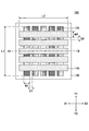
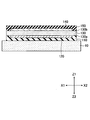
- FIG. 1 is a top view of the arrangement of the electrodes of the temperature sensor 100 in the present embodiment
- FIG. 2 is a cross-sectional view of the temperature sensor 100 cut along a dashed dotted line 1A-1B in FIG.
- the temperature sensor 100 measures the temperature of the surface of the measurement object 10 to be measured, and the first insulating layer 110, the first electrode 120, the polymer layer 130, the second The electrode 140, the second insulating layer 150, and the like are stacked in the Z1 direction from the Z2 direction side.
- a plurality of first electrodes 120 are formed on one surface 130 a of the polymer layer 130 with a film of a conductive metal material such as copper (Cu), silver (Ag), ITO (Indium Tin Oxide), or the like. .
- the first electrode 120 is formed to be long in the Y1-Y2 direction, and for example, the adjacent first electrodes 120 have a width W1 of about 5 mm, a length L1 of about 30 mm, and a thickness t1 of 8 to 16 ⁇ m.
- the distance G1 between the first electrode 120 and the first electrode 120 is formed to be about 60 ⁇ m.
- a plurality of second electrodes 140 are formed on the other surface 130 b of the polymer layer 130 using a film of a conductive metal material or the like such as copper, silver, or ITO.
- the second electrode 140 is formed to be long in the X1-X2 direction, and for example, the adjacent second electrode 140 has a width W2 of about 5 mm, a length L2 of about 30 mm, and a thickness t2 of 8 to 16 ⁇ m.
- a gap G2 between the second electrode 140 and the second electrode 140 is formed to be about 60 .mu.m.
- the extending direction of the first electrode 120 and the extending direction of the second electrode 140 are orthogonal to each other.
- the distance between the adjacent first electrode 120 and the first electrode 120 is referred to as the distance between the electrodes of the first electrode 120, and the adjacent second electrode 140 and the second electrode 140 are described. May be described as the distance between the electrodes of the second electrode 140.
- the temperature sensor shown in FIG. 1 and FIG. 2 etc. five first electrodes 120 are provided, and five second electrodes 140 are provided.
- the first insulating layer 110 is formed of a flexible insulating resin material so as to cover the first electrode 120 formed on one surface 130 a of the polymer layer 130, and has a thickness, for example. Is formed of a 40 ⁇ m polyimide or the like.
- the second insulating layer 150 is formed of a flexible insulating resin material so as to cover the second electrode 140 formed on the other surface 130 b of the polymer layer 130, and has a thickness, for example. Is formed of a 40 ⁇ m polyimide or the like.
- the polymer layer 130 is formed of a resin material having flexibility in which the relative dielectric constant changes as the temperature changes. Specifically, it is formed of polyimide or the like having a thickness d of 50 ⁇ m or less.
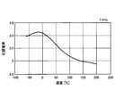
- FIG. 3 shows the relationship between the temperature and the relative dielectric constant of the polyimide when an alternating current of 1 kHz is applied. As shown in FIG. 3, when the temperature is -15.degree. C., the relative dielectric constant is about 3.45, and as the temperature rises, the relative dielectric constant gradually decreases, and when the temperature is 200.degree. C., the ratio is The dielectric constant is about 2.95.
- the linearity between the temperature and the relative dielectric constant will be described in the range of 20 ° C. to 100 ° C., which is relatively good.
- the relationship between the temperature and the relative dielectric constant is linear, and according to FIG. 3, the relative dielectric constant at a temperature of 20 ° C. is about 3.4, the temperature Assuming that the relative dielectric constant at 100 ° C. is about 3.1, the relative dielectric constant P is represented by the following equation (1).
- T is a temperature.
- the capacitance formed by the polymer layer 130 in a region sandwiched by the first electrode 120 and the second electrode 140 will be considered. Specifically, in a region where the first electrode 120 of width W1 where the first electrode 120 and the second electrode 140 intersect and the second electrode 140 of width W2 overlap, parallel plates at each intersection point If capacitors are to be formed, the area S of each parallel plate capacitor is 2.5 ⁇ 10 ⁇ 5 m 2 . In the examples shown in FIGS. 1 and 2, five first electrodes 120 and five second electrodes 140 are provided, and a total of 25 parallel plate capacitors are formed.
- the capacitance C at each intersection is expressed by the following equation (2).
- the vacuum dielectric constant ⁇ 0 is 8.85 ⁇ 10 12 .
- C P ⁇ ⁇ 0 ⁇ S / d (2)
- the relationship between the temperature and the capacitance when the thickness d of the polymer layer 130 is 12.5 ⁇ m (1.25 ⁇ 10 ⁇ 5 m) is shown in Table 2.
- the amount of change of the capacitance C at every 10 ° C. is about 0.66 pF (660 fF), and therefore, when the temperature changes by 1 ° C., The amount of change is about 66 fF. Since the resolution of the capacitance measuring device at present is 10 fF or more, the temperature resolution is about 0.15 ° C.
- the amount of change of the capacitance C at every 10 ° C. is about 0.33 pF (330 fF), and therefore, when the temperature changes by 1 ° C., The amount of change is about 33 fF.
- the resolution of the capacitance meter is the same as above, the resolution of the temperature is about 0.3.degree.
- the temperature resolution is about 0.6 ° C.
- the temperature resolution is about 0.9 ° C.
- the thickness d of the polymer layer 130 may be 75 ⁇ m considering that the temperature resolution is about 1 ° C., practically, the thickness d of the polymer layer 130 is 50 ⁇ m at which the temperature resolution is about 0.6 ° C or less It is preferable that it is the following.
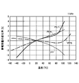
- FIG. 4 shows the relationship between the temperature and the rate of change of the capacitance measured by applying an alternating current of 1 kHz for PET, PEN, PP (Polypropylene), PPS (Poly Phenylene Sulfide), etc.
- the temperature sensor 100 in the present embodiment performs measurement by bringing the side of the first electrode 120 into contact with the surface of the measurement object 10 to be subjected to temperature measurement.
- the polymer layer 130, the first insulating layer 110, and the second insulating layer 150 are omitted in FIG. 5 for the sake of convenience, the omitted first insulating layer 110 is formed on the surface of the object 10 to be measured. Make contact and measure.
- the polymer layer 130, the first insulating layer 110, the second insulating layer 150, and the like are formed of a flexible material, and the first electrode 120 and the second electrode
- the electrode 140 is formed in a film shape and is extremely thin. For this reason, even if the surface of the measurement object 10 is not flat and is a curved surface or the like, it can be deformed according to the shape of the surface of the measurement object 10. Therefore, even when the surface of the measurement object 10 is a curved surface or the like, it can be brought into close contact and be in contact, and the temperature of the surface of the measurement object 10 can be measured accurately.
- the temperature measurement device in the present embodiment shown in FIG. 5 includes the temperature sensor 100, the temperature measurement unit 160, the display unit 170, and the like in the present embodiment.
- the temperature measurement unit 160 includes a capacitance detection unit 161, a calculation unit 162, a control unit 163, and the like.
- Each of the first electrode 120 and the second electrode 140 of the temperature sensor 100 is connected to the capacitance detection unit 161, and an alternating voltage is scanned and applied to the first electrode 120 and the second electrode.
- the capacitance formed between the first electrode 120 and the second electrode 140 is measured in each region where the electrodes 140 intersect with each other.
- the frequency of the alternating current applied when measuring the capacitance formed in each region of the temperature sensor 100 is preferably 1 kHz or more and 10 MHz or less.
- the calculation unit 162 calculates the temperature of each region based on the capacitance detection value in each region of the temperature sensor 100 detected by the capacitance detection unit 161.
- the control unit 163 controls the electrostatic capacitance detection unit 161 and the calculation unit 162, and the like.
- the display unit 170 is a display or the like capable of displaying a two-dimensional image, and can display information of temperature distribution in each region of the temperature sensor 100 obtained by the calculation unit 162 as a two-dimensional image.
- FIG. 6 shows a state in which the temperature distribution measured by the temperature sensor 100 in the present embodiment is displayed as a two-dimensional image on the display unit 170.
- FIG. 6 is a two-dimensional image of the temperature distribution obtained by the temperature sensor provided with five each of the first electrode 120 and the second electrode 140, but the first electrode 120 and the second electrode By increasing 140, more detailed two-dimensional temperature distribution information can be obtained.
- FIG. 7 shows a state of a two-dimensional image of a temperature distribution obtained by a temperature sensor provided with ten first electrodes 120 and ten second electrodes 140.
- the first electrode 120 and the second electrode 140 are formed of ITO or the like, and light is transmitted through the polymer layer 130, the first insulating layer 110, the second insulating layer 150, and the like. You may form with a material. In this case, since the surface of the measurement object 10 can be viewed through the temperature sensor, the temperature sensor can be easily attached to a desired position where the temperature of the surface of the measurement object 10 is to be measured.
- the temperature sensor measures the temperature by bringing the side of the first insulating layer 110 into contact with the surface of the measurement object 10, and therefore, between the first electrode 120 and the measurement object 10
- the first insulating layer 110 is preferably a material having a high thermal conductivity.
- the second insulating layer 150 is preferably formed of a material having a low thermal conductivity. Therefore, in the present embodiment, the first insulating layer 110 is preferably formed of a material having a thermal conductivity higher than that of the second insulating layer 150.
- thermal conductivity Materials that are flexible and have high thermal conductivity include heat-dissipating silicone rubber (thermal conductivity: 1 to 3 W / m ⁇ K) and thermally conductive double-sided adhesive tape (thermally conductive acrylic double-sided adhesive tape, thermally conductive Rate: 0.53 W / m ⁇ K) and the like.
- thermal conductivity of polyimide is about 0.16 W / m ⁇ K
- thermal conductivity of PET is about 0.14 W / m ⁇ K
- thermal conductivity of PEN is about 0.15 W / m ⁇ K.
- the first electrode 120 and the second electrode 140 are formed of copper having a thermal conductivity of 398 W / m ⁇ K, and the polymer layer 130 has a thermal conductivity of 0.16 W / m. It shall be formed of m ⁇ K polyimide. Therefore, the first electrode 120 and the second electrode 140 have a thermal conductivity of 2000 times or more that of the polymer layer 130.
- the distance G1 between the first electrodes 120 and the distance between the second electrodes 140 G2 is preferably formed wider than the thickness d of the polymer layer 130. If the distance G1 between the first electrodes 120 and the distance G2 between the second electrodes 140 are smaller than the thickness d of the polymer layer 130, the effect of the heat received from the adjacent region becomes large, and the temperature for each region That is, the temperature distribution can not be measured accurately.
- the first insulating layer 110 may be formed of a material having a thermal conductivity higher in the film thickness direction (Z1-Z2 direction) than in the in-plane direction (direction parallel to the XY plane).
- the in-plane direction is a direction perpendicular to the film thickness direction.
- thermal interference exerted on adjacent regions in the in-plane direction can be suppressed, and the heat transfer path can be divided for each region.
- a material is also called an anisotropic heat conductive material, and examples thereof include a graphite vertically oriented heat conductive sheet, and a material to which heat conductive anisotropy is imparted by controlling the structure of an organic polymer.
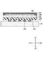
- the first insulating layer 110 may not be provided if the surface of the measurement target 10 to be subjected to the temperature measurement is an insulator. In the case where metal or the like is not expected to be in contact with the second electrode 140, the second insulating layer 150 may not be provided.
- the temperature sensor according to the present embodiment is formed of the first electrode 120, the polymer layer 130, and the second electrode 140, and the first electrode 120 is an object of temperature measurement. It may be in contact with the surface of the measurement object 10 to be
- the surface of the first insulating layer 110 that is, the side of the measurement object 10 causes the adhesive layer 180 to adhere to the surface of the measurement object 10. It may be provided on the surface of By forming such an adhesive layer 180, the temperature sensor can be brought into close contact with the surface of the measurement object 10 to be subjected to temperature measurement, and the temperature in each region can be accurately measured. That is, if there is a gap between the first insulating layer 110 and the surface of the measurement object 10, it is thermally insulated by the air existing in the gap, and the temperature of the surface of the measurement object 10 is accurately measured. Can not do it.
- the temperature sensor 100 can be adhered to the surface of the measurement object 10, and each region of the surface of the measurement object 10 It is possible to measure the exact temperature of The adhesive layer 180 may be integral with the first insulating layer 110.
- the adhesive layer 180 may, for example, be an acrylic double-sided adhesive tape or an acrylic double-sided adhesive tape of a PET substrate.
- a thermally conductive acrylic double-sided adhesive tape or the like having a thermal conductivity of 0.4 to 1.5 W / m ⁇ K may be used.
- the temperature sensor according to the present embodiment may have a pressure-sensitive adhesive layer 181 having insulation instead of the first insulating layer 110.
- the insulating adhesive layer 181 has both a function as an insulator and a function to be in close contact with the surface of the object to be measured 10.
- the adhesive layer 180 may be formed in a shape corresponding to the shape of the first electrode 120, and the shape of a region where the first electrode 120 and the second electrode 140 intersect. You may form in the shape corresponding to.
- thermal interference between adjacent regions can be further prevented.
- air is introduced between the adjacent adhesive layers 180 and thermally insulated, and therefore, they are also separated thermally.
- the size of the adhesive layer 180 may be smaller than the width of the first electrode 120, and the first electrode 120 and the second electrode 140 may be formed. You may form smaller than the area
- a third electrode 190 to be a shield electrode layer is formed of a material such as a metal on the second insulating layer 150, and the third electrode 190 is further formed.
- the third insulating layer 191 may be formed of a flexible and insulating resin material or the like so as to cover the electrode 190.
- the temperature sensor in the present embodiment is formed of the polymer layer 130 and the first electrode 120 and the second electrode 140 provided on both sides of the polymer layer 130, so that the temperature sensor can be miniaturized. It is possible and can be manufactured at low cost.
- the temperature sensor according to the present embodiment is not used for obtaining the temperature distribution of the surface of the measurement object 10, but as shown in FIG. 13 if it is simply used to measure the temperature of the surface of the measurement object 10.
- One each of the first electrode 120 and the second electrode 140 may be provided.
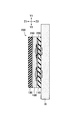
- FIG. 14 is a top view of the electrode arrangement of the temperature sensor 200 according to the present embodiment
- FIG. 14B is a cross-sectional view of the temperature sensor 200 taken along dashed dotted line 14A-14B in FIG. 14A
- 14C is a cross-sectional view of the temperature sensor 200 taken along dashed-dotted line 14C-14D in FIG. 14A.
- the temperature sensor 200 measures the temperature of the surface of the measurement object 10 to be subjected to the temperature measurement, and the first insulating layer 110, the first electrode 220, the polymer layer 130, the second The electrode 240, the second insulating layer 150, and the like are stacked in the Z1 direction from the Z2 direction side.
- the first electrode 220 and the second electrode 240 are formed of the same material as the first electrode 120 and the second electrode 140 in the first embodiment.
- a plurality of first electrodes 220 on the side of the measurement object 10 is formed, and the second electrode 220 on the opposite side to the side of the measurement object 10
- the one electrode 240 is formed so as to cover the entire first electrode 220.
- FIG. 15A is a top view of the electrode arrangement of the temperature sensor of this structure
- FIG. 15B is a cross-sectional view of the temperature sensor taken along dashed dotted line 15A-15B in FIG. 15A
- FIG. 15B is a cross-sectional view of the temperature sensor taken along dashed dotted line 15C-15D in FIG. 15A.
- the first electrode 920 and the second electrode 940 are formed of copper having a thermal conductivity of 398 W / m ⁇ K, and the polymer layer 130 is a polyimide having a thermal conductivity of 0.16 W / m ⁇ K. Shall be formed by Therefore, the first electrode 920 and the second electrode 940 have a thermal conductivity of 2000 times or more that of the polymer layer 130.
- the heat from the object to be measured 10 is transmitted to the first electrode 920 via the first insulating layer 110, as indicated by the dashed arrow.
- the first electrode 920 is formed of copper, the thermal conductivity is high, heat is transmitted in the in-plane direction, ie, in a direction parallel to the XY plane, and the entire surface of the first electrode 920 has substantially the same temperature. It will Since the first electrode 920 is formed over substantially the entire surface, the temperature of the entire polymer layer 130 is also substantially uniform, and the value of capacitance obtained through the plurality of second electrodes 940 is also substantially the same. It becomes. Therefore, in the temperature sensor having the structure shown in FIG. 15, even if the plurality of second electrodes 940 are provided, the detected temperatures are substantially the same, and the temperature distribution in each region of the surface of the measurement object 10 is measured You can not do it.
- the heat from the measurement object 10 is transferred to the first electrode 220 through the first insulating layer 110 as indicated by the dashed arrow. It is transmitted. Since the first electrode 220 is formed of copper, the thermal conductivity is high, but since the first electrode 220 is divided into a plurality of parts for each region, the temperature of the first electrode 220 is The temperature corresponds to the area. Therefore, since the temperature of the polymer layer 130 is also a temperature corresponding to each region of the first electrode 220, the value of the obtained capacitance is detected as a value reflecting the temperature distribution on the surface of the measurement object 10. Ru. Therefore, in the temperature sensor according to the present embodiment shown in FIG. 14, the temperature distribution on the surface of the measurement object 10 can be measured for each region of the plurality of first electrodes 220.
- the temperature sensor according to the present embodiment has a plurality of island-like regions in which the shapes of the first electrode and the second electrode are not strip-like and in which the temperature is measured, and connection regions connecting the island-like regions. It is formed by
- FIGS. 16 and 17 in the temperature sensor according to the present embodiment, a plurality of island regions 321 of the first electrode 320 are connected by the connection region 322, and the second electrode A plurality of island regions 341 are connected by a connection region 342.
- FIG. 16 is a view of the arrangement of the electrodes of the temperature sensor in the present embodiment from the top
- FIG. 17A is a view showing the arrangement of the first electrode 320
- FIG. Is a diagram showing the arrangement of FIG. 18 is a cross-sectional view taken along dashed dotted line 16A-16B in FIG.
- the first insulating layer 110, the first electrode 320, the polymer layer 130, the second electrode 340, the second insulating layer 150, and the like move in the Z1 direction from the Z2 direction. It is stacked.
- the first electrode 320 is a connection region 322 connecting the plurality of substantially square island regions 321 and the island regions 321 adjacent in the Y1-Y2 direction. And are formed.
- the size of the island-like region 321 of the first electrode 320 is a substantially square having a side length L11 of about 5 mm, and the island-like regions 321 adjacent in the Y1-Y2 direction are connected by the connection region 322 There is.
- the width L12 of the connection region 322 is narrower than the length L11 of one side of the island region 321, and is about 100 ⁇ m.
- the heat conduction in the connection region 322 becomes worse, so the thermal resolution in the adjacent island regions 321 can be improved. Accordingly, as shown in FIG. 17A, the island regions 321 adjacent in the Y1-Y2 direction are connected by the connection region 322, and five first electrodes 320 extending in the Y1-Y2 direction are provided.
- the second electrode 340 is formed of a plurality of substantially square island regions 341 and a connection region 342 connecting the island regions 341 adjacent in the X1-X2 direction. ing.
- the size of the island-like region 341 of the second electrode 340 is a substantially square having a side length L21 of about 5 mm, and the island-like regions 341 adjacent in the X1-X2 direction are connected by the connection region 342 There is.
- the width L22 of the connection region 342 is smaller than the length L21 of one side of the island region 341, and is about 100 ⁇ m.
- connection region 342 By narrowing the width L22 of the connection region 342, the heat conduction in the connection region 342 becomes worse, so the thermal resolution in the adjacent island regions 341 can be improved. Therefore, as shown in FIG. 17B, the island regions 341 adjacent in the X1-X2 direction are connected by the connection region 342, and five second electrodes 340 extending in the X1-X2 direction are provided.
- the island-like region 321 of the first electrode 320 and the island-like region 341 of the second electrode 340 are provided so as to overlap with each other. That is, in the present embodiment, the position of the insular region 321 of the first electrode 320 and the position of the insular region 341 of the second electrode 340 coincide in the X1-X2 direction and the Y1-Y2 direction, It is installed to overlap in the Z1-Z2 direction.
- a region is detected by detecting the capacitance of each region in which the polymer layer 130 is sandwiched between the island region 321 of the first electrode 320 and the island region 341 of the second electrode 340. Temperature measurement can be performed every time.
- thermal interference in each of the regions for detecting capacitance is formed by forming the narrow connection region 322 in the first electrode 320 and forming the narrow connection region 342 in the second electrode 340.
- the temperature distribution of the surface of the measurement object 10 can be accurately measured.
- FIG. 19 shows a temperature sensor according to the present embodiment, in which a first electrode 320 to which ten island regions 321 are connected and a second electrode 340 to which ten island regions 341 are connected are shown.
- the temperature sensor provided ten each, the result of having measured the temperature distribution of the surface of the measuring object 10 is shown typically.
- an adhesive layer 180 may be provided on the surface of the first insulating layer 110 to be in close contact with the surface of the object to be measured 10.
- the shape of the adhesive layer 180 is formed to be the same as or smaller than a region where the island-like region 321 of the first electrode 320 and the island-like region 341 of the second electrode 340 overlap. Furthermore, thermal interference can be suppressed.
- Measurement Object 100 Temperature Sensor 110 First Insulating Layer 120 First Electrode 130 Polymer Layer 130 a One Side 130 b Other Side 140 Second Electrode 150 Second Insulating Layer 160 Temperature Measurement Part 161 Capacitance Detection Part 162 operation unit 163 control unit 170 display unit 180 adhesive layer 190 third electrode 191 third insulating layer
Landscapes
- Engineering & Computer Science (AREA)
- Power Engineering (AREA)
- Physics & Mathematics (AREA)
- General Physics & Mathematics (AREA)
- Measuring Temperature Or Quantity Of Heat (AREA)
- Measuring And Recording Apparatus For Diagnosis (AREA)
- Radiation Pyrometers (AREA)
Abstract
This temperature sensor is characterized by having a polymer layer, a first electrode formed in one surface of the polymer layer, and a second electrode formed in the other surface of the polymer layer, wherein: the polymer layer has a relative permittivity that varies with temperature, and is composed of a flexible material; and the first electrode side is brought into contact with an object to be measured so as to measure the temperature of the object to be measured on the basis of the electrostatic capacitance of the polymer layer in a region sandwiched between the first and the second electrodes.
Description
本発明は、温度センサに関するものである。
The present invention relates to a temperature sensor.
温度を測定するための温度センサは、様々な分野において用いられており、温度を測定するための方法も様々である。例えば、従来からある温度計としては、アルコールや油又は水銀等の液体を用い、温度の変化により液体の体積が変化することを利用した温度計がある。また、近年では、サーミスタのように温度が変化すると電気抵抗が変化することを利用した温度計がある。更には、温度を測定する対象物が発する赤外線の波長及び強度等を検知することにより、その対象物の温度を測定する温度計もある。これらの温度計は、用途に応じて適した方式のものが使い分けられて使用されている。
Temperature sensors for measuring temperature are used in various fields, and methods for measuring temperature are also various. For example, as a conventional thermometer, there is a thermometer using a liquid such as alcohol, oil or mercury, and utilizing the fact that the volume of the liquid is changed by the change of temperature. Also, in recent years, there is a thermometer such as a thermistor that utilizes the change in electrical resistance when the temperature changes. Furthermore, there are also thermometers that measure the temperature of an object by detecting the wavelength and intensity of infrared light emitted by the object whose temperature is to be measured. These thermometers are properly used depending on the application.
このような温度計の中には、測定対象物の表面の温度を測定するための温度センサがあり、このような測定対象物の表面の温度を測定する温度センサにおいては、取扱が容易であって、小型で、低コストなものが求められている。
Among such thermometers, there is a temperature sensor for measuring the temperature of the surface of the measurement object, and the temperature sensor for measuring the temperature of the surface of the measurement object is easy to handle. Small, low cost products are required.
本実施の形態の一観点によれば、ポリマー層と、前記ポリマー層の一方の面に形成された第1の電極と、前記ポリマー層の他方の面に形成された第2の電極と、を有し、前記ポリマー層は、温度により比誘電率が変化するものであって、可撓性を有する材料により形成されており、測定対象物に前記第1の電極の側を接触させて、前記第1の電極と前記第2の電極との間に挟まれた領域の前記ポリマー層の静電容量に基づき、前記測定対象物の温度を測定することを特徴とする。
According to one aspect of the present embodiment, a polymer layer, a first electrode formed on one side of the polymer layer, and a second electrode formed on the other side of the polymer layer The polymer layer has a relative dielectric constant that changes with temperature, and is formed of a flexible material, and the object of measurement is brought into contact with the first electrode side, The temperature of the object to be measured is measured based on the capacitance of the polymer layer in a region sandwiched between the first electrode and the second electrode.
開示の温度センサによれば、測定対象物の表面の温度を測定する温度センサであって、取扱が容易で、小型で、低コストなものを得ることができる。
According to the disclosed temperature sensor, it is possible to obtain a temperature sensor that measures the temperature of the surface of the measurement object, which is easy to handle, small in size and low in cost.
実施するための形態について、以下に説明する。尚、同じ部材等については、同一の符号を付して説明を省略する。尚、本願においては、X1-X2方向、Y1-Y2方向、Z1-Z2方向を相互に直交する方向とする。また、X1-X2方向及びY1-Y2方向を含む面をXY面と記載し、Y1-Y2方向及びZ1-Z2方向を含む面をYZ面と記載し、Z1-Z2方向及びX1-X2方向を含む面をZX面と記載する。
A mode for carrying out will be described below. In addition, about the same member etc., the same code | symbol is attached | subjected and description is abbreviate | omitted. In the present application, the X1-X2 direction, the Y1-Y2 direction, and the Z1-Z2 direction are orthogonal to each other. In addition, a plane including the X1-X2 direction and the Y1-Y2 direction is described as an XY plane, a plane including the Y1-Y2 direction and the Z1-Z2 direction is described as the YZ plane, and the Z1-Z2 direction and the X1-X2 direction are described. The plane containing is described as ZX plane.
〔第1の実施の形態〕
第1の実施の形態における温度センサについて、図1及び図2に基づき説明する。図1は、本実施の形態における温度センサ100の電極の配置を上面から見た図であり、図2は、図1における一点鎖線1A-1Bにおいて切断した温度センサ100の断面図である。本実施の形態における温度センサ100は、温度測定の対象となる測定対象物10の表面の温度を測定するものであり、第1の絶縁層110、第1の電極120、ポリマー層130、第2の電極140、第2の絶縁層150等が、Z2方向の側からZ1方向に向かって積層されている。 First Embodiment
The temperature sensor in the first embodiment will be described based on FIG. 1 and FIG. FIG. 1 is a top view of the arrangement of the electrodes of thetemperature sensor 100 in the present embodiment, and FIG. 2 is a cross-sectional view of the temperature sensor 100 cut along a dashed dotted line 1A-1B in FIG. The temperature sensor 100 according to the present embodiment measures the temperature of the surface of the measurement object 10 to be measured, and the first insulating layer 110, the first electrode 120, the polymer layer 130, the second The electrode 140, the second insulating layer 150, and the like are stacked in the Z1 direction from the Z2 direction side.
第1の実施の形態における温度センサについて、図1及び図2に基づき説明する。図1は、本実施の形態における温度センサ100の電極の配置を上面から見た図であり、図2は、図1における一点鎖線1A-1Bにおいて切断した温度センサ100の断面図である。本実施の形態における温度センサ100は、温度測定の対象となる測定対象物10の表面の温度を測定するものであり、第1の絶縁層110、第1の電極120、ポリマー層130、第2の電極140、第2の絶縁層150等が、Z2方向の側からZ1方向に向かって積層されている。 First Embodiment
The temperature sensor in the first embodiment will be described based on FIG. 1 and FIG. FIG. 1 is a top view of the arrangement of the electrodes of the
第1の電極120は、ポリマー層130の一方の面130aに、銅(Cu)、銀(Ag)、ITO(Indium Tin Oxide)等の導電性を有する金属材料等の膜により複数形成されている。第1の電極120は、Y1-Y2方向に長く形成されており、例えば、幅W1が約5mm、長さL1が約30mm、厚さt1が8~16μmであり、隣り合う第1の電極120と第1の電極120との間隔G1は、約60μmとなるように形成されている。
A plurality of first electrodes 120 are formed on one surface 130 a of the polymer layer 130 with a film of a conductive metal material such as copper (Cu), silver (Ag), ITO (Indium Tin Oxide), or the like. . The first electrode 120 is formed to be long in the Y1-Y2 direction, and for example, the adjacent first electrodes 120 have a width W1 of about 5 mm, a length L1 of about 30 mm, and a thickness t1 of 8 to 16 μm. The distance G1 between the first electrode 120 and the first electrode 120 is formed to be about 60 μm.
第2の電極140は、ポリマー層130の他方の面130bに、銅、銀、ITO等の導電性を有する金属材料等の膜により複数形成されている。第2の電極140は、X1-X2方向に長く形成されており、例えば、幅W2が約5mm、長さL2が約30mm、厚さt2が8~16μmであり、隣り合う第2の電極140と第2の電極140との間隔G2は、約60μmとなるように形成されている。
A plurality of second electrodes 140 are formed on the other surface 130 b of the polymer layer 130 using a film of a conductive metal material or the like such as copper, silver, or ITO. The second electrode 140 is formed to be long in the X1-X2 direction, and for example, the adjacent second electrode 140 has a width W2 of about 5 mm, a length L2 of about 30 mm, and a thickness t2 of 8 to 16 μm. A gap G2 between the second electrode 140 and the second electrode 140 is formed to be about 60 .mu.m.
従って、第1の電極120の延びる方向と、第2の電極140の延びる方向とは直交している。尚、本願においては、隣り合う第1の電極120と第1の電極120との間隔を第1の電極120の電極間の間隔と記載し、隣り合う第2の電極140と第2の電極140との間隔を第2の電極140の電極間の間隔と記載する場合がある。図1及び図2等に示される温度センサでは、第1の電極120が5本設けられており、第2の電極140が5本設けられている。
Therefore, the extending direction of the first electrode 120 and the extending direction of the second electrode 140 are orthogonal to each other. In the present application, the distance between the adjacent first electrode 120 and the first electrode 120 is referred to as the distance between the electrodes of the first electrode 120, and the adjacent second electrode 140 and the second electrode 140 are described. May be described as the distance between the electrodes of the second electrode 140. In the temperature sensor shown in FIG. 1 and FIG. 2 etc., five first electrodes 120 are provided, and five second electrodes 140 are provided.
第1の絶縁層110は、ポリマー層130の一方の面130aに形成された第1の電極120を覆うように、可撓性を有する絶縁性の樹脂材料により形成されており、例えば、厚さが40μmのポリイミド等により形成されている。
The first insulating layer 110 is formed of a flexible insulating resin material so as to cover the first electrode 120 formed on one surface 130 a of the polymer layer 130, and has a thickness, for example. Is formed of a 40 μm polyimide or the like.
第2の絶縁層150は、ポリマー層130の他方の面130bに形成された第2の電極140を覆うように、可撓性を有する絶縁性の樹脂材料により形成されており、例えば、厚さが40μmのポリイミド等により形成されている。
The second insulating layer 150 is formed of a flexible insulating resin material so as to cover the second electrode 140 formed on the other surface 130 b of the polymer layer 130, and has a thickness, for example. Is formed of a 40 μm polyimide or the like.
ポリマー層130は、温度の変化に伴い比誘電率が変化する可撓性を有する樹脂材料により形成されている。具体的には、厚さdが50μm以下のポリイミド等により形成されている。図3は、1kHzの交流を印加した場合におけるポリイミドにおける温度と比誘電率との関係を示す。図3に示されるように、温度が-15℃の場合では比誘電率は約3.45であり、温度が高くなるに伴い比誘電率は徐々に減少し、温度が200℃の場合では比誘電率は約2.95となる。
The polymer layer 130 is formed of a resin material having flexibility in which the relative dielectric constant changes as the temperature changes. Specifically, it is formed of polyimide or the like having a thickness d of 50 μm or less. FIG. 3 shows the relationship between the temperature and the relative dielectric constant of the polyimide when an alternating current of 1 kHz is applied. As shown in FIG. 3, when the temperature is -15.degree. C., the relative dielectric constant is about 3.45, and as the temperature rises, the relative dielectric constant gradually decreases, and when the temperature is 200.degree. C., the ratio is The dielectric constant is about 2.95.
ここで、便宜上、温度と比誘電率との直線性が比較的良好な20℃~100℃の範囲において説明する。具体的には、温度が20℃~100℃の範囲では、温度と比誘電率との関係は直線的であるものとし、図3より温度が20℃の比誘電率は約3.4、温度が100℃の比誘電率は約3.1であるとした場合、比誘電率Pは下記(1)に示す式により表される。尚、Tは温度である。また、下記(1)に示す式のような直線の近似以外の近似でもよく、各値ごとの対応テーブルをあらかじめ有し、それに基づいて温度を得るものであってもよい
P=-0.00375×T+3.475・・・・・(1)
下記の表1は、上記(1)に示す式により得られた温度と比誘電率との関係を示す。
Here, for convenience, the linearity between the temperature and the relative dielectric constant will be described in the range of 20 ° C. to 100 ° C., which is relatively good. Specifically, in the temperature range of 20 ° C. to 100 ° C., the relationship between the temperature and the relative dielectric constant is linear, and according to FIG. 3, the relative dielectric constant at a temperature of 20 ° C. is about 3.4, the temperature Assuming that the relative dielectric constant at 100 ° C. is about 3.1, the relative dielectric constant P is represented by the following equation (1). Here, T is a temperature. Moreover, approximation other than approximation of a straight line like the formula shown in the following (1) may be used, and a correspondence table for each value may be provided in advance, and temperature may be obtained based thereon
P = -0.00375 × T + 3.475 (1)
Table 1 below shows the relationship between the temperature and the dielectric constant obtained by the equation shown in the above (1).

ここで、各々の交点における静電容量Cは、下記(2)に示す式により表される。尚、真空の誘電率ε0は8.85×10¹²である。
C=P×ε0×S/d・・・・・・(2)
ここで、ポリマー層130の厚さdを12.5μm(1.25×10⁻⁵m)とした場合における温度と静電容量の関係は、表2に示される。
Here, the capacitance C at each intersection is expressed by the following equation (2). The vacuum dielectric constant ε 0 is 8.85 × 10 12 .
C = P × ε 0 × S / d (2)
Here, the relationship between the temperature and the capacitance when the thickness d of thepolymer layer 130 is 12.5 μm (1.25 × 10 −5 m) is shown in Table 2.
C=P×ε0×S/d・・・・・・(2)
ここで、ポリマー層130の厚さdを12.5μm(1.25×10⁻⁵m)とした場合における温度と静電容量の関係は、表2に示される。
Here, the capacitance C at each intersection is expressed by the following equation (2). The vacuum dielectric constant ε 0 is 8.85 × 10 12 .
C = P × ε 0 × S / d (2)
Here, the relationship between the temperature and the capacitance when the thickness d of the

また、ポリマー層130の厚さdを25μm(2.5×10⁻⁵m)とした場合における温度と静電容量の関係は、表3に示される。
The relationship between the temperature and the capacitance when the thickness d of thepolymer layer 130 is 25 μm (2.5 × 10 −5 m) is shown in Table 3.
The relationship between the temperature and the capacitance when the thickness d of the

以上より、ポリマー層130の厚さdが50μmの場合では、温度の分解能は約0.6℃となり、ポリマー層130の厚さdが75μmの場合では、温度の分解能は約0.9℃となる。温度の分解能を約1℃と考えるとポリマー層130の厚さdは75μmでもよいが、実用的には、ポリマー層130の厚さdは、温度の分解能は約0.6℃以下となる50μm以下であることが好ましい。
From the above, when the thickness d of the polymer layer 130 is 50 μm, the temperature resolution is about 0.6 ° C. When the thickness d of the polymer layer 130 is 75 μm, the temperature resolution is about 0.9 ° C. Become. Although the thickness d of the polymer layer 130 may be 75 μm considering that the temperature resolution is about 1 ° C., practically, the thickness d of the polymer layer 130 is 50 μm at which the temperature resolution is about 0.6 ° C or less It is preferable that it is the following.
本実施の形態における温度センサにおいては、ポリマー層130には、図4に示されるように、ポリイミド以外にも、PET(polyethylene terephthalate)やPEN(polyethylene naphthalate)等を用いることも可能である。図4は、PETやPENの他、PP(Polypropylene)、PPS(Poly Phenylene Sulfide)等について、1kHzの交流を印加して測定した温度と静電容量の変化率との関係を示す。
In the temperature sensor according to the present embodiment, as shown in FIG. 4, it is also possible to use PET (polyethylene terephthalate), PEN (polyethylene naphthalate) or the like for the polymer layer 130 as shown in FIG. FIG. 4 shows the relationship between the temperature and the rate of change of the capacitance measured by applying an alternating current of 1 kHz for PET, PEN, PP (Polypropylene), PPS (Poly Phenylene Sulfide), etc.
(温度測定装置)
次に、図5に基づき本実施の形態における温度センサを用いた温度測定装置について説明する。本実施の形態における温度センサ100は、第1の電極120の側を温度測定の対象となる測定対象物10の表面に接触させて測定を行う。尚、図5では、便宜上、ポリマー層130や第1の絶縁層110及び第2の絶縁層150は省略されているが、省略されている第1の絶縁層110を測定対象物10の表面に接触させて測定を行う。本実施の形態における温度センサ100は、ポリマー層130や第1の絶縁層110及び第2の絶縁層150等が可撓性を有する材料により形成されており、第1の電極120及び第2の電極140は、膜状に形成されており極めて薄い。このため、測定対象物10の表面が平らではなく、曲面等の場合であっても、測定対象物10の表面の形状に対応して変形させることができる。よって、測定対象物10の表面が曲面等の場合であっても密着させて接触させることができ、測定対象物10の表面の温度を正確に測定することができる。 (Temperature measurement device)
Next, a temperature measurement device using a temperature sensor according to the present embodiment will be described based on FIG. Thetemperature sensor 100 in the present embodiment performs measurement by bringing the side of the first electrode 120 into contact with the surface of the measurement object 10 to be subjected to temperature measurement. Although the polymer layer 130, the first insulating layer 110, and the second insulating layer 150 are omitted in FIG. 5 for the sake of convenience, the omitted first insulating layer 110 is formed on the surface of the object 10 to be measured. Make contact and measure. In the temperature sensor 100 according to the present embodiment, the polymer layer 130, the first insulating layer 110, the second insulating layer 150, and the like are formed of a flexible material, and the first electrode 120 and the second electrode The electrode 140 is formed in a film shape and is extremely thin. For this reason, even if the surface of the measurement object 10 is not flat and is a curved surface or the like, it can be deformed according to the shape of the surface of the measurement object 10. Therefore, even when the surface of the measurement object 10 is a curved surface or the like, it can be brought into close contact and be in contact, and the temperature of the surface of the measurement object 10 can be measured accurately.
次に、図5に基づき本実施の形態における温度センサを用いた温度測定装置について説明する。本実施の形態における温度センサ100は、第1の電極120の側を温度測定の対象となる測定対象物10の表面に接触させて測定を行う。尚、図5では、便宜上、ポリマー層130や第1の絶縁層110及び第2の絶縁層150は省略されているが、省略されている第1の絶縁層110を測定対象物10の表面に接触させて測定を行う。本実施の形態における温度センサ100は、ポリマー層130や第1の絶縁層110及び第2の絶縁層150等が可撓性を有する材料により形成されており、第1の電極120及び第2の電極140は、膜状に形成されており極めて薄い。このため、測定対象物10の表面が平らではなく、曲面等の場合であっても、測定対象物10の表面の形状に対応して変形させることができる。よって、測定対象物10の表面が曲面等の場合であっても密着させて接触させることができ、測定対象物10の表面の温度を正確に測定することができる。 (Temperature measurement device)
Next, a temperature measurement device using a temperature sensor according to the present embodiment will be described based on FIG. The
図5に示される本実施の形態における温度測定装置は、本実施の形態における温度センサ100、温度測定部160、表示部170等を有している。温度測定部160は、静電容量検出部161、演算部162、制御部163等を有している。静電容量検出部161には、温度センサ100の第1の電極120及び第2の電極140の各々が接続されており、交流電圧を走査しながら印加して、第1の電極120と第2の電極140とが交差する各々の領域において、第1の電極120と第2の電極140との間に形成される静電容量を測定する。温度センサ100の各々の領域に形成される静電容量を測定する際に印加する交流の周波数は、1kHz以上、10MHz以下が好ましい。
The temperature measurement device in the present embodiment shown in FIG. 5 includes the temperature sensor 100, the temperature measurement unit 160, the display unit 170, and the like in the present embodiment. The temperature measurement unit 160 includes a capacitance detection unit 161, a calculation unit 162, a control unit 163, and the like. Each of the first electrode 120 and the second electrode 140 of the temperature sensor 100 is connected to the capacitance detection unit 161, and an alternating voltage is scanned and applied to the first electrode 120 and the second electrode. The capacitance formed between the first electrode 120 and the second electrode 140 is measured in each region where the electrodes 140 intersect with each other. The frequency of the alternating current applied when measuring the capacitance formed in each region of the temperature sensor 100 is preferably 1 kHz or more and 10 MHz or less.
演算部162は、静電容量検出部161において検出された温度センサ100の各々の領域における静電容量検出値に基づき、各々の領域の温度を算出する。制御部163は、静電容量検出部161及び演算部162の制御等を行う。表示部170は、2次元画像を表示することのできるディスプレイ等であり、演算部162において得られた温度センサ100の各々の領域における温度分布の情報を2次元画像として表示することができる。
The calculation unit 162 calculates the temperature of each region based on the capacitance detection value in each region of the temperature sensor 100 detected by the capacitance detection unit 161. The control unit 163 controls the electrostatic capacitance detection unit 161 and the calculation unit 162, and the like. The display unit 170 is a display or the like capable of displaying a two-dimensional image, and can display information of temperature distribution in each region of the temperature sensor 100 obtained by the calculation unit 162 as a two-dimensional image.
図6は、本実施の形態における温度センサ100により測定された温度分布を表示部170において2次元画像として表示した場合の様子を示す。図6は、第1の電極120及び第2の電極140が各々5本ずつ設けられている温度センサにより得られた温度分布の2次元画像であるが、第1の電極120及び第2の電極140を増やすことにより、更に詳細な2次元の温度分布の情報を得ることができる。図7には、第1の電極120及び第2の電極140が各々10本ずつ設けられている温度センサにより得られた温度分布の2次元画像の様子を示す。
FIG. 6 shows a state in which the temperature distribution measured by the temperature sensor 100 in the present embodiment is displayed as a two-dimensional image on the display unit 170. FIG. 6 is a two-dimensional image of the temperature distribution obtained by the temperature sensor provided with five each of the first electrode 120 and the second electrode 140, but the first electrode 120 and the second electrode By increasing 140, more detailed two-dimensional temperature distribution information can be obtained. FIG. 7 shows a state of a two-dimensional image of a temperature distribution obtained by a temperature sensor provided with ten first electrodes 120 and ten second electrodes 140.
本実施の形態における温度センサでは、第1の電極120及び第2の電極140をITO等により形成し、ポリマー層130、第1の絶縁層110及び第2の絶縁層150等を光を透過する材料により形成してもよい。この場合、温度センサを透過して測定対象物10の表面を目視することができるため、測定対象物10の表面の温度を測定したい所望の位置に、温度センサを容易に取り付けることができる。
In the temperature sensor according to this embodiment, the first electrode 120 and the second electrode 140 are formed of ITO or the like, and light is transmitted through the polymer layer 130, the first insulating layer 110, the second insulating layer 150, and the like. You may form with a material. In this case, since the surface of the measurement object 10 can be viewed through the temperature sensor, the temperature sensor can be easily attached to a desired position where the temperature of the surface of the measurement object 10 is to be measured.
(温度センサにおける熱伝導)
本実施の形態における温度センサは、第1の絶縁層110の側を測定対象物10の表面に接触させて温度を測定するものであるため、第1の電極120と測定対象物10との間の第1の絶縁層110は、熱伝導率が高い材料であることが好ましい。また、外部からの熱の影響を避けるため、第2の絶縁層150は、熱伝導率が低い材料により形成されていることが好ましい。従って、本実施の形態は、第1の絶縁層110は、第2の絶縁層150よりも、熱伝導率の高い材料により形成されていることが好ましい。 (Thermal conduction in the temperature sensor)
The temperature sensor according to the present embodiment measures the temperature by bringing the side of the first insulatinglayer 110 into contact with the surface of the measurement object 10, and therefore, between the first electrode 120 and the measurement object 10 The first insulating layer 110 is preferably a material having a high thermal conductivity. In order to avoid the influence of external heat, the second insulating layer 150 is preferably formed of a material having a low thermal conductivity. Therefore, in the present embodiment, the first insulating layer 110 is preferably formed of a material having a thermal conductivity higher than that of the second insulating layer 150.
本実施の形態における温度センサは、第1の絶縁層110の側を測定対象物10の表面に接触させて温度を測定するものであるため、第1の電極120と測定対象物10との間の第1の絶縁層110は、熱伝導率が高い材料であることが好ましい。また、外部からの熱の影響を避けるため、第2の絶縁層150は、熱伝導率が低い材料により形成されていることが好ましい。従って、本実施の形態は、第1の絶縁層110は、第2の絶縁層150よりも、熱伝導率の高い材料により形成されていることが好ましい。 (Thermal conduction in the temperature sensor)
The temperature sensor according to the present embodiment measures the temperature by bringing the side of the first insulating
可撓性があって熱伝導率の高い材料としては、放熱シリコーンゴム(熱伝導率:1~3W/m・K)や熱伝導性両面粘着テープ(熱伝導性アクリル系両面粘着テープ、熱伝導率:0.53W/m・K)等が挙げられる。また、可撓性があって熱伝導率の低い材料としては、アクリル発泡体や発泡プラスチック等の空気が内包されているものが挙げられる。尚、ポリイミドの熱伝導率は約0.16W/m・K、PETの熱伝導率は約0.14W/m・K、PENの熱伝導率は約0.15W/m・Kである。
Materials that are flexible and have high thermal conductivity include heat-dissipating silicone rubber (thermal conductivity: 1 to 3 W / m · K) and thermally conductive double-sided adhesive tape (thermally conductive acrylic double-sided adhesive tape, thermally conductive Rate: 0.53 W / m · K) and the like. Moreover, as a material which is flexible and has a low thermal conductivity, a material containing air such as an acrylic foam or a foamed plastic can be mentioned. The thermal conductivity of polyimide is about 0.16 W / m · K, the thermal conductivity of PET is about 0.14 W / m · K, and the thermal conductivity of PEN is about 0.15 W / m · K.
本実施の形態においては、第1の電極120、第2の電極140は、熱伝導率が398W/m・Kの銅により形成されており、ポリマー層130は、熱伝導率が0.16W/m・Kのポリイミドにより形成されているものとする。従って、第1の電極120、第2の電極140は、ポリマー層130に比べて、熱伝導率が2000倍以上である。
In the present embodiment, the first electrode 120 and the second electrode 140 are formed of copper having a thermal conductivity of 398 W / m · K, and the polymer layer 130 has a thermal conductivity of 0.16 W / m. It shall be formed of m · K polyimide. Therefore, the first electrode 120 and the second electrode 140 have a thermal conductivity of 2000 times or more that of the polymer layer 130.
また、静電容量を検出するそれぞれの電極相互の熱的干渉、即ち、隣の領域から受ける熱的影響をできるだけ避けるためには、第1の電極120の間隔G1及び第2の電極140の間隔G2は、ポリマー層130の厚さdよりも広く形成されていることが好ましい。第1の電極120の間隔G1及び第2の電極140の間隔G2が、ポリマー層130の厚さdよりも狭いと、隣の領域から受ける熱の影響が大きくなり、各々の領域ごとの温度、すなわち温度分布を正確に測定することができなくなるからである。
In addition, in order to avoid thermal interference between the respective electrodes for detecting capacitance, that is, thermal effects from adjacent areas as much as possible, the distance G1 between the first electrodes 120 and the distance between the second electrodes 140 G2 is preferably formed wider than the thickness d of the polymer layer 130. If the distance G1 between the first electrodes 120 and the distance G2 between the second electrodes 140 are smaller than the thickness d of the polymer layer 130, the effect of the heat received from the adjacent region becomes large, and the temperature for each region That is, the temperature distribution can not be measured accurately.
また、第1の絶縁層110は、面内方向(XY面に平行な方向)よりも、膜厚方向(Z1-Z2方向)における熱伝導率が高い材料により形成してもよい。尚、面内方向とは、膜厚方向に対し垂直となる方向である。これにより、面内方向において隣り合う領域に及ぼす熱的干渉を抑制することができ、各々の領域ごとに熱の伝達経路を分けることができる。このような材料は、異方性熱伝導材料とも呼ばれるものであり、黒鉛垂直配向熱伝導シートや、有機ポリマーの構造を制御することにより熱伝導異方性が付与されたもの等が挙げられる。
Further, the first insulating layer 110 may be formed of a material having a thermal conductivity higher in the film thickness direction (Z1-Z2 direction) than in the in-plane direction (direction parallel to the XY plane). The in-plane direction is a direction perpendicular to the film thickness direction. Thus, thermal interference exerted on adjacent regions in the in-plane direction can be suppressed, and the heat transfer path can be divided for each region. Such a material is also called an anisotropic heat conductive material, and examples thereof include a graphite vertically oriented heat conductive sheet, and a material to which heat conductive anisotropy is imparted by controlling the structure of an organic polymer.
本実施の形態における温度センサは、温度測定の対象となる測定対象物10の表面が絶縁体であれば、第1の絶縁層110を設けなくてもよい場合がある。また、第2の電極140に、金属等が接触することが想定されない場合には、第2の絶縁層150を設けなくともよい場合がある。具体的には、本実施の形態における温度センサは、図8に示すように、第1の電極120、ポリマー層130、第2の電極140により形成され、第1の電極120を温度測定の対象となる測定対象物10の表面に接触させるものであってもよい。
In the temperature sensor according to the present embodiment, the first insulating layer 110 may not be provided if the surface of the measurement target 10 to be subjected to the temperature measurement is an insulator. In the case where metal or the like is not expected to be in contact with the second electrode 140, the second insulating layer 150 may not be provided. Specifically, as shown in FIG. 8, the temperature sensor according to the present embodiment is formed of the first electrode 120, the polymer layer 130, and the second electrode 140, and the first electrode 120 is an object of temperature measurement. It may be in contact with the surface of the measurement object 10 to be
(粘着層)
また、本実施の形態における温度センサは、図9に示すように、測定対象物10の表面に密着させるための粘着層180を第1の絶縁層110の表面、即ち、測定対象物10の側の面に設けたものであってもよい。このような粘着層180を形成することにより、温度測定の対象となる測定対象物10の表面に、温度センサを密着させることができ、各々の領域における温度を正確に測定することができる。即ち、第1の絶縁層110と測定対象物10の表面との間に隙間があると、その隙間に存在している空気等により断熱され、測定対象物10の表面の温度を正確には測定することができない。よって、温度センサの第1の絶縁層110の表面に粘着層180を設けることにより、測定対象物10の表面に温度センサ100を密着させることができ、測定対象物10の表面の各々の領域ごとの正確な温度を測定することが可能となる。尚、粘着層180は、第1の絶縁層110と一体となっているものであってもよい。 (Adhesive layer)
In the temperature sensor according to the present embodiment, as shown in FIG. 9, the surface of the first insulatinglayer 110, that is, the side of the measurement object 10, causes the adhesive layer 180 to adhere to the surface of the measurement object 10. It may be provided on the surface of By forming such an adhesive layer 180, the temperature sensor can be brought into close contact with the surface of the measurement object 10 to be subjected to temperature measurement, and the temperature in each region can be accurately measured. That is, if there is a gap between the first insulating layer 110 and the surface of the measurement object 10, it is thermally insulated by the air existing in the gap, and the temperature of the surface of the measurement object 10 is accurately measured. Can not do it. Therefore, by providing the adhesive layer 180 on the surface of the first insulating layer 110 of the temperature sensor, the temperature sensor 100 can be adhered to the surface of the measurement object 10, and each region of the surface of the measurement object 10 It is possible to measure the exact temperature of The adhesive layer 180 may be integral with the first insulating layer 110.
また、本実施の形態における温度センサは、図9に示すように、測定対象物10の表面に密着させるための粘着層180を第1の絶縁層110の表面、即ち、測定対象物10の側の面に設けたものであってもよい。このような粘着層180を形成することにより、温度測定の対象となる測定対象物10の表面に、温度センサを密着させることができ、各々の領域における温度を正確に測定することができる。即ち、第1の絶縁層110と測定対象物10の表面との間に隙間があると、その隙間に存在している空気等により断熱され、測定対象物10の表面の温度を正確には測定することができない。よって、温度センサの第1の絶縁層110の表面に粘着層180を設けることにより、測定対象物10の表面に温度センサ100を密着させることができ、測定対象物10の表面の各々の領域ごとの正確な温度を測定することが可能となる。尚、粘着層180は、第1の絶縁層110と一体となっているものであってもよい。 (Adhesive layer)
In the temperature sensor according to the present embodiment, as shown in FIG. 9, the surface of the first insulating
粘着層180としては、アクリル系両面テープやPET基材のアクリル系両面テープ等が挙げられる。また、粘着層180を熱伝導性の高い材料により形成する場合には、熱伝導率が0.4~1.5W/m・Kの熱伝導性アクリル系両面粘着テープ等を用いてもよい。
The adhesive layer 180 may, for example, be an acrylic double-sided adhesive tape or an acrylic double-sided adhesive tape of a PET substrate. When the adhesive layer 180 is formed of a material having high thermal conductivity, a thermally conductive acrylic double-sided adhesive tape or the like having a thermal conductivity of 0.4 to 1.5 W / m · K may be used.
更に、本実施の形態における温度センサは、図10に示すように、第1の絶縁層110に代えて、絶縁性を有する粘着層181を形成したものであってもよい。絶縁性を有する粘着層181であれば、絶縁体としての機能と、測定対象物10の表面に密着させる機能の双方を併せ持つからである。
Furthermore, as shown in FIG. 10, the temperature sensor according to the present embodiment may have a pressure-sensitive adhesive layer 181 having insulation instead of the first insulating layer 110. The insulating adhesive layer 181 has both a function as an insulator and a function to be in close contact with the surface of the object to be measured 10.
図11に示すように、粘着層180は、第1の電極120の形状に対応した形状で形成してもよく、また、第1の電極120と第2の電極140とが交差する領域の形状に対応した形状で形成してもよい。このように、粘着層180を分離して形成することにより、隣り合う領域間において相互に及ぼす熱的干渉をより一層防ぐことができる。具体的には、粘着層180を分離して形成することにより、隣り合う粘着層180間には空気が入り込み断熱されるため、熱的にも分離されるからである。
As shown in FIG. 11, the adhesive layer 180 may be formed in a shape corresponding to the shape of the first electrode 120, and the shape of a region where the first electrode 120 and the second electrode 140 intersect. You may form in the shape corresponding to. By separately forming the adhesive layer 180 in this manner, thermal interference between adjacent regions can be further prevented. Specifically, by forming the adhesive layer 180 separately, air is introduced between the adjacent adhesive layers 180 and thermally insulated, and therefore, they are also separated thermally.
また、この場合、図11に示すように、粘着層180の大きさは、第1の電極120の幅よりも小さく形成してもよく、また、第1の電極120と第2の電極140とが交差する領域よりも小さく形成してもよい。粘着層180を第1の電極120等よりも小さく形成することにより、隣の領域に熱が伝わるのを抑制することができ、温度分布をより正確に測定することができる。
Further, in this case, as shown in FIG. 11, the size of the adhesive layer 180 may be smaller than the width of the first electrode 120, and the first electrode 120 and the second electrode 140 may be formed. You may form smaller than the area | region which 2 By forming the adhesive layer 180 smaller than the first electrode 120 or the like, it is possible to suppress the transfer of heat to the adjacent region, and the temperature distribution can be measured more accurately.
また、本実施の形態は、図12に示すように、第2の絶縁層150の上に、金属等の材料によりシールド電極層となる第3の電極190を形成し、更に、この第3の電極190を覆うように、可撓性及び絶縁性を有する樹脂材料等により第3の絶縁層191を形成したものであってもよい。第1の電極120及び第2の電極140を略覆うように第3の電極190を形成することにより、外部からの電気的影響、例えば、Z1方向の側からの電気的影響を防ぐことができ、温度測定を正確に行うことができる。
Further, in the present embodiment, as shown in FIG. 12, a third electrode 190 to be a shield electrode layer is formed of a material such as a metal on the second insulating layer 150, and the third electrode 190 is further formed. The third insulating layer 191 may be formed of a flexible and insulating resin material or the like so as to cover the electrode 190. By forming the third electrode 190 so as to substantially cover the first electrode 120 and the second electrode 140, it is possible to prevent an external electrical influence, for example, an electrical influence from the Z1 direction side. , Temperature measurement can be performed accurately.
本実施の形態における温度センサは、ポリマー層130と、ポリマー層130の両面に設けられた第1の電極120及び第2の電極140等により形成されているため、温度センサを小型にすることが可能であり、また、低コストで製造することができる。
The temperature sensor in the present embodiment is formed of the polymer layer 130 and the first electrode 120 and the second electrode 140 provided on both sides of the polymer layer 130, so that the temperature sensor can be miniaturized. It is possible and can be manufactured at low cost.
尚、本実施の形態における温度センサは、測定対象物10の表面の温度分布を得る用途ではなく、単に測定対象物10の表面の温度を測定する用途であれば、図13に示すように、第1の電極120及び第2の電極140を各々一つずつ設けたものであってもよい。
The temperature sensor according to the present embodiment is not used for obtaining the temperature distribution of the surface of the measurement object 10, but as shown in FIG. 13 if it is simply used to measure the temperature of the surface of the measurement object 10. One each of the first electrode 120 and the second electrode 140 may be provided.
〔第2の実施の形態〕
次に、第2の実施の形態の温度センサについて説明する。本実施の形態は、図14に示すように、第1の電極は複数設けられており、第2の電極は一体で形成されている構造のものである。図14Aは、本実施の形態における温度センサ200の電極の配置を上面から見た図であり、図14Bは、図14Aにおける一点鎖線14A-14Bにおいて温度センサ200を切断した断面図であり、図14Cは、図14Aにおける一点鎖線14C-14Dにおいて温度センサ200を切断した断面図である。 Second Embodiment
Next, a temperature sensor according to a second embodiment will be described. In this embodiment, as shown in FIG. 14, a plurality of first electrodes are provided, and a second electrode is integrally formed. 14A is a top view of the electrode arrangement of thetemperature sensor 200 according to the present embodiment, and FIG. 14B is a cross-sectional view of the temperature sensor 200 taken along dashed dotted line 14A-14B in FIG. 14A. 14C is a cross-sectional view of the temperature sensor 200 taken along dashed-dotted line 14C-14D in FIG. 14A.
次に、第2の実施の形態の温度センサについて説明する。本実施の形態は、図14に示すように、第1の電極は複数設けられており、第2の電極は一体で形成されている構造のものである。図14Aは、本実施の形態における温度センサ200の電極の配置を上面から見た図であり、図14Bは、図14Aにおける一点鎖線14A-14Bにおいて温度センサ200を切断した断面図であり、図14Cは、図14Aにおける一点鎖線14C-14Dにおいて温度センサ200を切断した断面図である。 Second Embodiment
Next, a temperature sensor according to a second embodiment will be described. In this embodiment, as shown in FIG. 14, a plurality of first electrodes are provided, and a second electrode is integrally formed. 14A is a top view of the electrode arrangement of the
本実施の形態における温度センサ200は、温度測定の対象となる測定対象物10の表面の温度を測定するものであり、第1の絶縁層110、第1の電極220、ポリマー層130、第2の電極240、第2の絶縁層150等が、Z2方向の側からZ1方向に向かって積層されている構造のものである。本実施の形態においては、第1の電極220及び第2の電極240は、第1の実施の形態における第1の電極120及び第2の電極140と同様の材料等により形成されている。
The temperature sensor 200 according to the present embodiment measures the temperature of the surface of the measurement object 10 to be subjected to the temperature measurement, and the first insulating layer 110, the first electrode 220, the polymer layer 130, the second The electrode 240, the second insulating layer 150, and the like are stacked in the Z1 direction from the Z2 direction side. In the present embodiment, the first electrode 220 and the second electrode 240 are formed of the same material as the first electrode 120 and the second electrode 140 in the first embodiment.
本実施の形態における温度センサは、図14に示されるように、測定対象物10の側となる第1の電極220は複数形成されており、測定対象物10の側とは反対側の第2の電極240は、第1の電極220の全体を覆うように1つ形成されている。
In the temperature sensor according to the present embodiment, as shown in FIG. 14, a plurality of first electrodes 220 on the side of the measurement object 10 is formed, and the second electrode 220 on the opposite side to the side of the measurement object 10 The one electrode 240 is formed so as to cover the entire first electrode 220.
ここで、本実施の形態における温度センサについて、図15に示す構造の温度センサと比較しながら説明する。図15に示す構造の温度センサは、測定対象物10の側とは反対側には第2の電極940が複数形成されており、測定対象物10の側には略全面を覆う第1の電極920が1つ形成されている。図15Aは、この構造の温度センサの電極の配置を上面から見た図であり、図15Bは、図15Aにおける一点鎖線15A-15Bにおいて、この温度センサを切断した断面図であり、図15Cは、図15Aにおける一点鎖線15C-15Dにおいて、この温度センサを切断した断面図である。
Here, the temperature sensor in the present embodiment will be described in comparison with the temperature sensor having the structure shown in FIG. In the temperature sensor having the structure shown in FIG. 15, a plurality of second electrodes 940 are formed on the side opposite to the side of the measurement object 10, and the first electrode covering substantially the entire surface on the side of the measurement object 10 One 920 is formed. 15A is a top view of the electrode arrangement of the temperature sensor of this structure, FIG. 15B is a cross-sectional view of the temperature sensor taken along dashed dotted line 15A-15B in FIG. 15A, and FIG. FIG. 15B is a cross-sectional view of the temperature sensor taken along dashed dotted line 15C-15D in FIG. 15A.
尚、第1の電極920、第2の電極940は、熱伝導率が398W/m・Kの銅により形成されており、ポリマー層130は、熱伝導率が0.16W/m・Kのポリイミドにより形成されているものとする。従って、第1の電極920、第2の電極940は、ポリマー層130に比べて、熱伝導率が2000倍以上である。
The first electrode 920 and the second electrode 940 are formed of copper having a thermal conductivity of 398 W / m · K, and the polymer layer 130 is a polyimide having a thermal conductivity of 0.16 W / m · K. Shall be formed by Therefore, the first electrode 920 and the second electrode 940 have a thermal conductivity of 2000 times or more that of the polymer layer 130.
この場合、図15に示す構造の温度センサでは、測定対象物10からの熱は、破線矢印に示すように、第1の絶縁層110を介し第1の電極920に伝わる。第1の電極920は銅により形成されているため、熱伝導率が高く、熱は面内方向、即ち、XY面に平行な方向に伝わり、第1の電極920の全面が略同じ温度となってしまう。第1の電極920は略全面に形成されているため、ポリマー層130の全体の温度も略均一な温度となり、複数の第2の電極940を介して得られる静電容量の値も略同じ値となる。従って、図15に示す構造の温度センサでは、複数の第2の電極940が設けられていても、検出される温度は略同じとなり、測定対象物10の表面の各々の領域における温度分布を測定することはできない。
In this case, in the temperature sensor having the structure shown in FIG. 15, the heat from the object to be measured 10 is transmitted to the first electrode 920 via the first insulating layer 110, as indicated by the dashed arrow. Since the first electrode 920 is formed of copper, the thermal conductivity is high, heat is transmitted in the in-plane direction, ie, in a direction parallel to the XY plane, and the entire surface of the first electrode 920 has substantially the same temperature. It will Since the first electrode 920 is formed over substantially the entire surface, the temperature of the entire polymer layer 130 is also substantially uniform, and the value of capacitance obtained through the plurality of second electrodes 940 is also substantially the same. It becomes. Therefore, in the temperature sensor having the structure shown in FIG. 15, even if the plurality of second electrodes 940 are provided, the detected temperatures are substantially the same, and the temperature distribution in each region of the surface of the measurement object 10 is measured You can not do it.
これに対し、本実施の形態における温度センサでは、図14に示すように、測定対象物10からの熱は、破線矢印に示すように、第1の絶縁層110を介し第1の電極220に伝わる。第1の電極220は銅により形成されているため熱伝導率は高いが、第1の電極220は各々の領域ごとに複数に分割されているため、第1の電極220の温度は、各々の領域に対応した温度となる。従って、ポリマー層130の温度も、第1の電極220の各々の領域に対応した温度となるため、得られる静電容量の値は測定対象物10の表面の温度分布を反映した値として検出される。よって、図14に示される本実施の形態における温度センサでは、複数の第1の電極220の領域ごとに、測定対象物10の表面の温度分布を測定することができる。
On the other hand, in the temperature sensor according to the present embodiment, as shown in FIG. 14, the heat from the measurement object 10 is transferred to the first electrode 220 through the first insulating layer 110 as indicated by the dashed arrow. It is transmitted. Since the first electrode 220 is formed of copper, the thermal conductivity is high, but since the first electrode 220 is divided into a plurality of parts for each region, the temperature of the first electrode 220 is The temperature corresponds to the area. Therefore, since the temperature of the polymer layer 130 is also a temperature corresponding to each region of the first electrode 220, the value of the obtained capacitance is detected as a value reflecting the temperature distribution on the surface of the measurement object 10. Ru. Therefore, in the temperature sensor according to the present embodiment shown in FIG. 14, the temperature distribution on the surface of the measurement object 10 can be measured for each region of the plurality of first electrodes 220.
尚、上記以外の内容については、第1の実施の形態と同様である。
The contents other than the above are the same as in the first embodiment.
〔第3の実施の形態〕
次に、第3の実施の形態における温度センサについて説明する。本実施の形態における温度センサは、第1の電極及び第2の電極の形状が帯状ではなく、温度が測定される領域となる複数の島状領域と、島状領域を接続する接続領域と、により形成されている。 Third Embodiment
Next, a temperature sensor in the third embodiment will be described. The temperature sensor according to the present embodiment has a plurality of island-like regions in which the shapes of the first electrode and the second electrode are not strip-like and in which the temperature is measured, and connection regions connecting the island-like regions. It is formed by
具体的には、本実施の形態における温度センサは、図16及び図17に示すように、第1の電極320は複数の島状領域321が接続領域322により接続されており、第2の電極340は複数の島状領域341が接続領域342により接続されている。図16は、本実施の形態における温度センサの電極の配置を上面から見た図であり、図17Aは、第1の電極320の配置を示す図であり、図17Bは、第2の電極340の配置を示す図である。図18は、図16における一点鎖線16A-16Bにおいて切断した断面図である。
Specifically, as shown in FIGS. 16 and 17, in the temperature sensor according to the present embodiment, a plurality of island regions 321 of the first electrode 320 are connected by the connection region 322, and the second electrode A plurality of island regions 341 are connected by a connection region 342. FIG. 16 is a view of the arrangement of the electrodes of the temperature sensor in the present embodiment from the top, FIG. 17A is a view showing the arrangement of the first electrode 320, and FIG. Is a diagram showing the arrangement of FIG. 18 is a cross-sectional view taken along dashed dotted line 16A-16B in FIG.
本実施の形態における温度センサは、第1の絶縁層110、第1の電極320、ポリマー層130、第2の電極340、第2の絶縁層150等が、Z2方向の側からZ1方向に向かって積層されている。
In the temperature sensor according to the present embodiment, the first insulating layer 110, the first electrode 320, the polymer layer 130, the second electrode 340, the second insulating layer 150, and the like move in the Z1 direction from the Z2 direction. It is stacked.
本実施の形態においては、図17Aに示されるように、第1の電極320は、複数の略正方形の島状領域321と、Y1-Y2方向において隣り合う島状領域321を接続する接続領域322とにより形成されている。第1の電極320の島状領域321の大きさは、一辺の長さL11が約5mmの略正方形であり、Y1-Y2方向において隣り合う島状領域321同士は、接続領域322により接続されている。接続領域322の幅L12は、島状領域321の一辺の長さL11よりも狭く形成されており、約100μmである。接続領域322の幅L12を狭くすることにより、接続領域322における熱伝導は悪くなるため、隣り合う島状領域321における熱的分解能を向上させることができる。従って、図17Aに示すように、Y1-Y2方向において隣り合う島状領域321が接続領域322により接続されており、Y1-Y2方向に延びる第1の電極320が5つ設けられている。
In the present embodiment, as shown in FIG. 17A, the first electrode 320 is a connection region 322 connecting the plurality of substantially square island regions 321 and the island regions 321 adjacent in the Y1-Y2 direction. And are formed. The size of the island-like region 321 of the first electrode 320 is a substantially square having a side length L11 of about 5 mm, and the island-like regions 321 adjacent in the Y1-Y2 direction are connected by the connection region 322 There is. The width L12 of the connection region 322 is narrower than the length L11 of one side of the island region 321, and is about 100 μm. By narrowing the width L12 of the connection region 322, the heat conduction in the connection region 322 becomes worse, so the thermal resolution in the adjacent island regions 321 can be improved. Accordingly, as shown in FIG. 17A, the island regions 321 adjacent in the Y1-Y2 direction are connected by the connection region 322, and five first electrodes 320 extending in the Y1-Y2 direction are provided.
同様に、第2の電極340は、図17Bに示されるように、複数の略正方形の島状領域341と、X1-X2方向において隣り合う島状領域341を接続する接続領域342とにより形成されている。第2の電極340の島状領域341の大きさは、一辺の長さL21が約5mmの略正方形であり、X1-X2方向において隣り合う島状領域341同士は、接続領域342により接続されている。接続領域342の幅L22は、島状領域341の一辺の長さL21よりも狭く形成されており、約100μmである。接続領域342の幅L22を狭くすることにより、接続領域342における熱伝導は悪くなるため、隣り合う島状領域341における熱的分解能を向上させることができる。従って、図17Bに示すように、X1-X2方向において隣り合う島状領域341が接続領域342により接続されており、X1-X2方向に延びる第2の電極340が5つ設けられている。
Similarly, as shown in FIG. 17B, the second electrode 340 is formed of a plurality of substantially square island regions 341 and a connection region 342 connecting the island regions 341 adjacent in the X1-X2 direction. ing. The size of the island-like region 341 of the second electrode 340 is a substantially square having a side length L21 of about 5 mm, and the island-like regions 341 adjacent in the X1-X2 direction are connected by the connection region 342 There is. The width L22 of the connection region 342 is smaller than the length L21 of one side of the island region 341, and is about 100 μm. By narrowing the width L22 of the connection region 342, the heat conduction in the connection region 342 becomes worse, so the thermal resolution in the adjacent island regions 341 can be improved. Therefore, as shown in FIG. 17B, the island regions 341 adjacent in the X1-X2 direction are connected by the connection region 342, and five second electrodes 340 extending in the X1-X2 direction are provided.
本実施の形態においては、第1の電極320における島状領域321と第2の電極340における島状領域341とが重なるように設置されている。即ち、本実施の形態においては、第1の電極320の島状領域321の位置と第2の電極340の島状領域341の位置とが、X1-X2方向及びY1-Y2方向において一致し、Z1-Z2方向において重なるように設置されている。本実施の形態においては、ポリマー層130が第1の電極320の島状領域321と第2の電極340の島状領域341とにより挟まれた領域ごとの静電容量を検出することで、領域ごとに温度測定を行うことができる。
In the present embodiment, the island-like region 321 of the first electrode 320 and the island-like region 341 of the second electrode 340 are provided so as to overlap with each other. That is, in the present embodiment, the position of the insular region 321 of the first electrode 320 and the position of the insular region 341 of the second electrode 340 coincide in the X1-X2 direction and the Y1-Y2 direction, It is installed to overlap in the Z1-Z2 direction. In this embodiment, a region is detected by detecting the capacitance of each region in which the polymer layer 130 is sandwiched between the island region 321 of the first electrode 320 and the island region 341 of the second electrode 340. Temperature measurement can be performed every time.
このように、第1の電極320に幅の狭い接続領域322を形成し、第2の電極340に幅の狭い接続領域342を形成することにより、静電容量を検出する領域ごとの熱的干渉を抑制することができ、測定対象物10の表面の温度分布を正確に測定することができる。
Thus, thermal interference in each of the regions for detecting capacitance is formed by forming the narrow connection region 322 in the first electrode 320 and forming the narrow connection region 342 in the second electrode 340. The temperature distribution of the surface of the measurement object 10 can be accurately measured.
図19は、本実施の形態における温度センサにおいて、10個の島状領域321が接続された第1の電極320と、10個の島状領域341が接続された第2の電極340とが、各々10本ずつ設けられている温度センサにおいて、測定対象物10の表面の温度分布を測定した結果を模式的に示すものである。
19 shows a temperature sensor according to the present embodiment, in which a first electrode 320 to which ten island regions 321 are connected and a second electrode 340 to which ten island regions 341 are connected are shown. In the temperature sensor provided ten each, the result of having measured the temperature distribution of the surface of the measuring object 10 is shown typically.
更に、本実施の形態は、図20に示すように、第1の絶縁層110の表面に、測定対象物10の表面と密着させるための粘着層180を設けてもよい。この際、粘着層180の形状は、第1の電極320の島状領域321と、第2の電極340の島状領域341とが重なる領域と同じ、または、それよりも小さく形成することにより、更に、熱的干渉を抑制することができる。
Furthermore, in the present embodiment, as shown in FIG. 20, an adhesive layer 180 may be provided on the surface of the first insulating layer 110 to be in close contact with the surface of the object to be measured 10. At this time, the shape of the adhesive layer 180 is formed to be the same as or smaller than a region where the island-like region 321 of the first electrode 320 and the island-like region 341 of the second electrode 340 overlap. Furthermore, thermal interference can be suppressed.
尚、上記以外の内容については、第1の実施の形態と同様である。
The contents other than the above are the same as in the first embodiment.
以上、実施の形態について詳述したが、特定の実施形態に限定されるものではなく、特許請求の範囲に記載された範囲内において、種々の変形及び変更が可能である。
As mentioned above, although an embodiment was explained in full detail, it is not limited to a specific embodiment, and various modification and change are possible within the limits indicated in a claim.
尚、本国際出願は、2017年7月20日に出願した米国仮出願62/534745に基づく優先権を主張するものであり、その出願の全内容は本国際出願に援用する。
This international application claims priority based on US Provisional Application 62 / 534,745 filed July 20, 2017, the entire content of which is incorporated herein by reference.
10 測定対象物
100 温度センサ
110 第1の絶縁層
120 第1の電極
130 ポリマー層
130a 一方の面
130b 他方の面
140 第2の電極
150 第2の絶縁層
160 温度測定部
161 静電容量検出部
162 演算部
163 制御部
170 表示部
180 粘着層
190 第3の電極
191 第3の絶縁層 10Measurement Object 100 Temperature Sensor 110 First Insulating Layer 120 First Electrode 130 Polymer Layer 130 a One Side 130 b Other Side 140 Second Electrode 150 Second Insulating Layer 160 Temperature Measurement Part 161 Capacitance Detection Part 162 operation unit 163 control unit 170 display unit 180 adhesive layer 190 third electrode 191 third insulating layer
100 温度センサ
110 第1の絶縁層
120 第1の電極
130 ポリマー層
130a 一方の面
130b 他方の面
140 第2の電極
150 第2の絶縁層
160 温度測定部
161 静電容量検出部
162 演算部
163 制御部
170 表示部
180 粘着層
190 第3の電極
191 第3の絶縁層 10
Claims (12)
- ポリマー層と、
前記ポリマー層の一方の面に形成された第1の電極と、
前記ポリマー層の他方の面に形成された第2の電極と、
を有し、
前記ポリマー層は、温度により比誘電率が変化するものであって、可撓性を有する材料により形成されており、
測定対象物に前記第1の電極の側を接触させて、前記第1の電極と前記第2の電極との間に挟まれた領域の前記ポリマー層の静電容量に基づき、前記測定対象物の温度を測定することを特徴とする温度センサ。 A polymer layer,
A first electrode formed on one side of the polymer layer;
A second electrode formed on the other side of the polymer layer;
Have
The polymer layer has a dielectric constant that changes with temperature, and is formed of a flexible material.
The object to be measured is brought into contact with the side of the first electrode, and the object to be measured is determined based on the capacitance of the polymer layer in a region sandwiched between the first electrode and the second electrode. A temperature sensor characterized by measuring the temperature of - 前記ポリマー層の一方の面に形成された前記第1の電極を覆う第1の絶縁層を有することを特徴とする請求項1に記載の温度センサ。 The temperature sensor according to claim 1, further comprising a first insulating layer covering the first electrode formed on one surface of the polymer layer.
- 前記第1の絶縁層は、膜厚方向における熱伝導率が、面内方向よりも高いことを特徴とする請求項2に記載の温度センサ。 3. The temperature sensor according to claim 2, wherein the thermal conductivity in the film thickness direction of the first insulating layer is higher than that in the in-plane direction.
- 前記ポリマー層の他方の面に形成された前記第2の電極を覆う第2の絶縁層を有し、
前記第1の絶縁層の膜厚方向における熱伝導率は、前記第2の絶縁層の膜厚方向における熱伝導率よりも高いことを特徴とする請求項2または3に記載の温度センサ。 A second insulating layer covering the second electrode formed on the other side of the polymer layer,
4. The temperature sensor according to claim 2, wherein a thermal conductivity in a film thickness direction of the first insulating layer is higher than a thermal conductivity in a film thickness direction of the second insulating layer. - 前記第2の絶縁層の上には、第3の電極が設けられていることを特徴とする請求項4に記載の温度センサ。 The temperature sensor according to claim 4, wherein a third electrode is provided on the second insulating layer.
- 前記第1の絶縁層には、前記測定対象物の表面に接触する粘着層が設けられていることを特徴とする請求項2から5のいずれかに記載の温度センサ。 The temperature sensor according to any one of claims 2 to 5, wherein an adhesive layer in contact with the surface of the measurement object is provided on the first insulating layer.
- 前記第1の電極は複数設けられており、
前記第1の電極と前記第2の電極との間に挟まれた複数の領域の前記ポリマー層の静電容量に基づき前記測定対象物の温度分布を測定することを特徴とする請求項1から6のいずれかに記載の温度センサ。 A plurality of the first electrodes are provided,
The temperature distribution of the object to be measured is measured based on the capacitance of the polymer layer in a plurality of regions sandwiched between the first electrode and the second electrode. The temperature sensor according to any one of 6. - 前記第1の電極は複数設けられており、
前記第2の電極は複数設けられており、
前記第1の電極の延びる方向と、前記第2の電極の延びる方向とは、略直交するものであって、
前記第1の電極と前記第2の電極との間に挟まれた複数の領域の前記ポリマー層の静電容量に基づき前記測定対象物の温度分布を測定することを特徴とする請求項1から6のいずれかに記載の温度センサ。 A plurality of the first electrodes are provided,
A plurality of the second electrodes are provided,
The extending direction of the first electrode and the extending direction of the second electrode are substantially orthogonal to each other,
The temperature distribution of the object to be measured is measured based on the capacitance of the polymer layer in a plurality of regions sandwiched between the first electrode and the second electrode. The temperature sensor according to any one of 6. - 前記ポリマー層の厚さは、隣り合う前記第1の電極間の間隔よりも短いことを特徴とする請求項7または8に記載の温度センサ。 The temperature sensor according to claim 7 or 8, wherein the thickness of the polymer layer is smaller than the distance between the adjacent first electrodes.
- 前記ポリマー層は、ポリイミド、PETまたはPENのうちのいずれかを含むものにより形成されていることを特徴とする請求項1から9のいずれかに記載の温度センサ。 The temperature sensor according to any one of claims 1 to 9, wherein the polymer layer is formed of one containing polyimide, PET or PEN.
- 前記静電容量は、前記第1の電極と前記第2の電極との間に、交流電圧を印加して得られた値であることを特徴とする請求項1から10のいずれかに記載の温度センサ。 11. The capacitance according to any one of claims 1 to 10, wherein the capacitance is a value obtained by applying an alternating voltage between the first electrode and the second electrode. Temperature sensor.
- 前記ポリマー層の厚さは、50μm以下であることを特徴とする請求項1から11のいずれかに記載の温度センサ。 The temperature sensor according to any one of claims 1 to 11, wherein a thickness of the polymer layer is 50 μm or less.
Priority Applications (2)
| Application Number | Priority Date | Filing Date | Title |
|---|---|---|---|
| JP2019530892A JP6932782B2 (en) | 2017-07-20 | 2018-05-09 | Temperature sensor |
| US16/743,463 US11300459B2 (en) | 2017-07-20 | 2020-01-15 | Capacitive temperature sensor |
Applications Claiming Priority (2)
| Application Number | Priority Date | Filing Date | Title |
|---|---|---|---|
| US201762534745P | 2017-07-20 | 2017-07-20 | |
| US62/534,745 | 2017-07-20 |
Related Child Applications (1)
| Application Number | Title | Priority Date | Filing Date |
|---|---|---|---|
| US16/743,463 Continuation US11300459B2 (en) | 2017-07-20 | 2020-01-15 | Capacitive temperature sensor |
Publications (1)
| Publication Number | Publication Date |
|---|---|
| WO2019017045A1 true WO2019017045A1 (en) | 2019-01-24 |
Family
ID=65015074
Family Applications (1)
| Application Number | Title | Priority Date | Filing Date |
|---|---|---|---|
| PCT/JP2018/017896 WO2019017045A1 (en) | 2017-07-20 | 2018-05-09 | Temperature sensor |
Country Status (3)
| Country | Link |
|---|---|
| US (1) | US11300459B2 (en) |
| JP (1) | JP6932782B2 (en) |
| WO (1) | WO2019017045A1 (en) |
Cited By (2)
| Publication number | Priority date | Publication date | Assignee | Title |
|---|---|---|---|---|
| CN111537098A (en) * | 2020-04-08 | 2020-08-14 | 中山大学 | Flexible capacitive temperature sensor and manufacturing method thereof |
| KR20220012765A (en) * | 2020-07-23 | 2022-02-04 | 광운대학교 산학협력단 | Wearable temperature sensors based on metal-ion doped high-k metal-oxide dielectrics operating at low-voltage and high-frequency for healthcare monitoring systems |
Citations (6)
| Publication number | Priority date | Publication date | Assignee | Title |
|---|---|---|---|---|
| JP2002111087A (en) * | 2000-09-29 | 2002-04-12 | Matsushita Electric Ind Co Ltd | Flexible piezoelectric element and abnormality monitor employing it |
| JP2005172839A (en) * | 2005-02-03 | 2005-06-30 | Matsushita Electric Ind Co Ltd | Temperature measurement system |
| JP2005233708A (en) * | 2004-02-18 | 2005-09-02 | Ishikawajima Harima Heavy Ind Co Ltd | Capacitance type load cell |
| JP2009192306A (en) * | 2008-02-13 | 2009-08-27 | Wacom Co Ltd | Position detecting device |
| JP2010210400A (en) * | 2009-03-10 | 2010-09-24 | Daikin Ind Ltd | Element for detecting abnormal high temperature and device for detecting abnormally high temperature equipped with the same |
| JP2015507185A (en) * | 2012-01-02 | 2015-03-05 | コミッサリア ア レネルジー アトミーク エ オ ゼネルジ ザルタナテイヴ | Capacitive temperature sensor with two capacitors as voltage divider bridge |
Family Cites Families (5)
| Publication number | Priority date | Publication date | Assignee | Title |
|---|---|---|---|---|
| US5021795A (en) * | 1989-06-23 | 1991-06-04 | Motorola, Inc. | Passive temperature compensation scheme for microstrip antennas |
| FI98567C (en) * | 1993-09-29 | 1997-07-10 | Vaisala Oy | Impedance sensor, especially for radio probe use, as well as a method for producing a sensor |
| US6359444B1 (en) * | 1999-05-28 | 2002-03-19 | University Of Kentucky Research Foundation | Remote resonant-circuit analyte sensing apparatus with sensing structure and associated method of sensing |
| JP6026447B2 (en) * | 2014-01-17 | 2016-11-16 | 富士フイルム株式会社 | Laminate for touch panel, flat panel display |
| JP2016091052A (en) | 2014-10-29 | 2016-05-23 | 京セラ株式会社 | Electronic device |
-
2018
- 2018-05-09 JP JP2019530892A patent/JP6932782B2/en active Active
- 2018-05-09 WO PCT/JP2018/017896 patent/WO2019017045A1/en active Application Filing
-
2020
- 2020-01-15 US US16/743,463 patent/US11300459B2/en active Active
Patent Citations (6)
| Publication number | Priority date | Publication date | Assignee | Title |
|---|---|---|---|---|
| JP2002111087A (en) * | 2000-09-29 | 2002-04-12 | Matsushita Electric Ind Co Ltd | Flexible piezoelectric element and abnormality monitor employing it |
| JP2005233708A (en) * | 2004-02-18 | 2005-09-02 | Ishikawajima Harima Heavy Ind Co Ltd | Capacitance type load cell |
| JP2005172839A (en) * | 2005-02-03 | 2005-06-30 | Matsushita Electric Ind Co Ltd | Temperature measurement system |
| JP2009192306A (en) * | 2008-02-13 | 2009-08-27 | Wacom Co Ltd | Position detecting device |
| JP2010210400A (en) * | 2009-03-10 | 2010-09-24 | Daikin Ind Ltd | Element for detecting abnormal high temperature and device for detecting abnormally high temperature equipped with the same |
| JP2015507185A (en) * | 2012-01-02 | 2015-03-05 | コミッサリア ア レネルジー アトミーク エ オ ゼネルジ ザルタナテイヴ | Capacitive temperature sensor with two capacitors as voltage divider bridge |
Cited By (4)
| Publication number | Priority date | Publication date | Assignee | Title |
|---|---|---|---|---|
| CN111537098A (en) * | 2020-04-08 | 2020-08-14 | 中山大学 | Flexible capacitive temperature sensor and manufacturing method thereof |
| CN111537098B (en) * | 2020-04-08 | 2021-07-13 | 中山大学 | Flexible capacitive temperature sensor and manufacturing method thereof |
| KR20220012765A (en) * | 2020-07-23 | 2022-02-04 | 광운대학교 산학협력단 | Wearable temperature sensors based on metal-ion doped high-k metal-oxide dielectrics operating at low-voltage and high-frequency for healthcare monitoring systems |
| KR102424918B1 (en) * | 2020-07-23 | 2022-07-25 | 광운대학교 산학협력단 | Wearable temperature sensors based on metal-ion doped high-k metal-oxide dielectrics operating at low-voltage and high-frequency for healthcare monitoring systems |
Also Published As
| Publication number | Publication date |
|---|---|
| US20200149978A1 (en) | 2020-05-14 |
| JP6932782B2 (en) | 2021-09-08 |
| JPWO2019017045A1 (en) | 2020-07-02 |
| US11300459B2 (en) | 2022-04-12 |
Similar Documents
| Publication | Publication Date | Title |
|---|---|---|
| JP6562357B2 (en) | Pressure sensor | |
| Nassar et al. | Paper skin multisensory platform for simultaneous environmental monitoring | |
| US9222846B2 (en) | Tactile sensor | |
| US10591523B2 (en) | Capacitive sensor and manufacturing method thereof | |
| US10553655B2 (en) | Force sensor device and OLED display device including the same | |
| JP2013020370A5 (en) | ||
| JP6932782B2 (en) | Temperature sensor | |
| CN107110716B (en) | Sensor sheet | |
| JP2015513068A (en) | Thermal image sensor | |
| JP6468398B2 (en) | Deep thermometer | |
| US8393209B2 (en) | Capacitive detector, method for manufacturing same, and device for measuring the integral | |
| JP7205770B2 (en) | Composite sensor | |
| US9016937B2 (en) | Sensor | |
| Park et al. | Pixel-free capacitive touch sensor using a single-layer ion gel | |
| US10591360B2 (en) | Thermal sensor with two superposed pyroelectric portions for measuring a charge differential | |
| KR100990087B1 (en) | Array-type Flexible Thin Film Temperature Sensor and the Fabrication Method Thereof | |
| JP2007333670A (en) | Thermal mass flowmeter | |
| KR101530189B1 (en) | Touchscreen apparatus having multiple bar-type transparent electrodes | |
| JP7152708B2 (en) | capacitive sensor | |
| GB2522639A (en) | An apparatus and associated methods for temperature sensing | |
| WO2015025487A1 (en) | Touch panel | |
| JP2013190346A (en) | Capacitance type liquid level sensor | |
| JP2020016484A (en) | Temperature sensor | |
| JP2016169978A (en) | Infrared sensor | |
| Fan et al. | Evaluation of printed capacitive touch sensors for touch panel |
Legal Events
| Date | Code | Title | Description |
|---|---|---|---|
| 121 | Ep: the epo has been informed by wipo that ep was designated in this application |
Ref document number: 18835136 Country of ref document: EP Kind code of ref document: A1 |
|
| ENP | Entry into the national phase |
Ref document number: 2019530892 Country of ref document: JP Kind code of ref document: A |
|
| NENP | Non-entry into the national phase |
Ref country code: DE |
|
| 122 | Ep: pct application non-entry in european phase |
Ref document number: 18835136 Country of ref document: EP Kind code of ref document: A1 |