WO2019007136A1 - 阵列基板、其制备方法和显示面板 - Google Patents
阵列基板、其制备方法和显示面板 Download PDFInfo
- Publication number
- WO2019007136A1 WO2019007136A1 PCT/CN2018/083983 CN2018083983W WO2019007136A1 WO 2019007136 A1 WO2019007136 A1 WO 2019007136A1 CN 2018083983 W CN2018083983 W CN 2018083983W WO 2019007136 A1 WO2019007136 A1 WO 2019007136A1
- Authority
- WO
- WIPO (PCT)
- Prior art keywords
- electrode
- data line
- connection electrode
- sub
- gate
- Prior art date
- Legal status (The legal status is an assumption and is not a legal conclusion. Google has not performed a legal analysis and makes no representation as to the accuracy of the status listed.)
- Ceased
Links
Images




Classifications
-
- H—ELECTRICITY
- H10—SEMICONDUCTOR DEVICES; ELECTRIC SOLID-STATE DEVICES NOT OTHERWISE PROVIDED FOR
- H10D—INORGANIC ELECTRIC SEMICONDUCTOR DEVICES
- H10D86/00—Integrated devices formed in or on insulating or conducting substrates, e.g. formed in silicon-on-insulator [SOI] substrates or on stainless steel or glass substrates
- H10D86/40—Integrated devices formed in or on insulating or conducting substrates, e.g. formed in silicon-on-insulator [SOI] substrates or on stainless steel or glass substrates characterised by multiple TFTs
-
- H—ELECTRICITY
- H10—SEMICONDUCTOR DEVICES; ELECTRIC SOLID-STATE DEVICES NOT OTHERWISE PROVIDED FOR
- H10D—INORGANIC ELECTRIC SEMICONDUCTOR DEVICES
- H10D86/00—Integrated devices formed in or on insulating or conducting substrates, e.g. formed in silicon-on-insulator [SOI] substrates or on stainless steel or glass substrates
- H10D86/40—Integrated devices formed in or on insulating or conducting substrates, e.g. formed in silicon-on-insulator [SOI] substrates or on stainless steel or glass substrates characterised by multiple TFTs
- H10D86/421—Integrated devices formed in or on insulating or conducting substrates, e.g. formed in silicon-on-insulator [SOI] substrates or on stainless steel or glass substrates characterised by multiple TFTs having a particular composition, shape or crystalline structure of the active layer
-
- H—ELECTRICITY
- H10—SEMICONDUCTOR DEVICES; ELECTRIC SOLID-STATE DEVICES NOT OTHERWISE PROVIDED FOR
- H10D—INORGANIC ELECTRIC SEMICONDUCTOR DEVICES
- H10D86/00—Integrated devices formed in or on insulating or conducting substrates, e.g. formed in silicon-on-insulator [SOI] substrates or on stainless steel or glass substrates
- H10D86/01—Manufacture or treatment
- H10D86/021—Manufacture or treatment of multiple TFTs
-
- H—ELECTRICITY
- H10—SEMICONDUCTOR DEVICES; ELECTRIC SOLID-STATE DEVICES NOT OTHERWISE PROVIDED FOR
- H10D—INORGANIC ELECTRIC SEMICONDUCTOR DEVICES
- H10D86/00—Integrated devices formed in or on insulating or conducting substrates, e.g. formed in silicon-on-insulator [SOI] substrates or on stainless steel or glass substrates
- H10D86/01—Manufacture or treatment
- H10D86/021—Manufacture or treatment of multiple TFTs
- H10D86/0221—Manufacture or treatment of multiple TFTs comprising manufacture, treatment or patterning of TFT semiconductor bodies
-
- H—ELECTRICITY
- H10—SEMICONDUCTOR DEVICES; ELECTRIC SOLID-STATE DEVICES NOT OTHERWISE PROVIDED FOR
- H10D—INORGANIC ELECTRIC SEMICONDUCTOR DEVICES
- H10D86/00—Integrated devices formed in or on insulating or conducting substrates, e.g. formed in silicon-on-insulator [SOI] substrates or on stainless steel or glass substrates
- H10D86/40—Integrated devices formed in or on insulating or conducting substrates, e.g. formed in silicon-on-insulator [SOI] substrates or on stainless steel or glass substrates characterised by multiple TFTs
- H10D86/441—Interconnections, e.g. scanning lines
-
- H—ELECTRICITY
- H10—SEMICONDUCTOR DEVICES; ELECTRIC SOLID-STATE DEVICES NOT OTHERWISE PROVIDED FOR
- H10D—INORGANIC ELECTRIC SEMICONDUCTOR DEVICES
- H10D86/00—Integrated devices formed in or on insulating or conducting substrates, e.g. formed in silicon-on-insulator [SOI] substrates or on stainless steel or glass substrates
- H10D86/40—Integrated devices formed in or on insulating or conducting substrates, e.g. formed in silicon-on-insulator [SOI] substrates or on stainless steel or glass substrates characterised by multiple TFTs
- H10D86/60—Integrated devices formed in or on insulating or conducting substrates, e.g. formed in silicon-on-insulator [SOI] substrates or on stainless steel or glass substrates characterised by multiple TFTs wherein the TFTs are in active matrices
-
- H—ELECTRICITY
- H10—SEMICONDUCTOR DEVICES; ELECTRIC SOLID-STATE DEVICES NOT OTHERWISE PROVIDED FOR
- H10W—GENERIC PACKAGES, INTERCONNECTIONS, CONNECTORS OR OTHER CONSTRUCTIONAL DETAILS OF DEVICES COVERED BY CLASS H10
- H10W42/00—Arrangements for protection of devices
- H10W42/20—Arrangements for protection of devices protecting against electromagnetic or particle radiation, e.g. light, X-rays, gamma-rays or electrons
-
- G—PHYSICS
- G02—OPTICS
- G02F—OPTICAL DEVICES OR ARRANGEMENTS FOR THE CONTROL OF LIGHT BY MODIFICATION OF THE OPTICAL PROPERTIES OF THE MEDIA OF THE ELEMENTS INVOLVED THEREIN; NON-LINEAR OPTICS; FREQUENCY-CHANGING OF LIGHT; OPTICAL LOGIC ELEMENTS; OPTICAL ANALOGUE/DIGITAL CONVERTERS
- G02F1/00—Devices or arrangements for the control of the intensity, colour, phase, polarisation or direction of light arriving from an independent light source, e.g. switching, gating or modulating; Non-linear optics
- G02F1/01—Devices or arrangements for the control of the intensity, colour, phase, polarisation or direction of light arriving from an independent light source, e.g. switching, gating or modulating; Non-linear optics for the control of the intensity, phase, polarisation or colour
- G02F1/13—Devices or arrangements for the control of the intensity, colour, phase, polarisation or direction of light arriving from an independent light source, e.g. switching, gating or modulating; Non-linear optics for the control of the intensity, phase, polarisation or colour based on liquid crystals, e.g. single liquid crystal display cells
- G02F1/133—Constructional arrangements; Operation of liquid crystal cells; Circuit arrangements
- G02F1/136—Liquid crystal cells structurally associated with a semi-conducting layer or substrate, e.g. cells forming part of an integrated circuit
- G02F1/1362—Active matrix addressed cells
- G02F1/136286—Wiring, e.g. gate line, drain line
-
- G—PHYSICS
- G02—OPTICS
- G02F—OPTICAL DEVICES OR ARRANGEMENTS FOR THE CONTROL OF LIGHT BY MODIFICATION OF THE OPTICAL PROPERTIES OF THE MEDIA OF THE ELEMENTS INVOLVED THEREIN; NON-LINEAR OPTICS; FREQUENCY-CHANGING OF LIGHT; OPTICAL LOGIC ELEMENTS; OPTICAL ANALOGUE/DIGITAL CONVERTERS
- G02F1/00—Devices or arrangements for the control of the intensity, colour, phase, polarisation or direction of light arriving from an independent light source, e.g. switching, gating or modulating; Non-linear optics
- G02F1/01—Devices or arrangements for the control of the intensity, colour, phase, polarisation or direction of light arriving from an independent light source, e.g. switching, gating or modulating; Non-linear optics for the control of the intensity, phase, polarisation or colour
- G02F1/13—Devices or arrangements for the control of the intensity, colour, phase, polarisation or direction of light arriving from an independent light source, e.g. switching, gating or modulating; Non-linear optics for the control of the intensity, phase, polarisation or colour based on liquid crystals, e.g. single liquid crystal display cells
- G02F1/133—Constructional arrangements; Operation of liquid crystal cells; Circuit arrangements
- G02F1/136—Liquid crystal cells structurally associated with a semi-conducting layer or substrate, e.g. cells forming part of an integrated circuit
- G02F1/1362—Active matrix addressed cells
- G02F1/1368—Active matrix addressed cells in which the switching element is a three-electrode device
Definitions
- the present disclosure relates to the field of display technologies, and in particular, to an array substrate, a method of fabricating the same, and a display panel.
- a widely used method is to form a source, a drain, and an active layer with the same halftone mask (HTM MASK) to reduce the number of masks.
- HTM MASK halftone mask
- this method generally causes an increase in leakage current of a thin film transistor (TFT) and deteriorates performance of the TFT. Therefore, the current manufacturing method of the array substrate still needs to be improved.
- TFT thin film transistor
- Embodiments of the present disclosure relate to an array basic, a method of fabricating the same, and a display panel.
- an array substrate is proposed.
- the array substrate includes: a base substrate; a thin film transistor disposed on one side of the base substrate, and including a first electrode, a second electrode, and a gate; and a data line
- the data line is disposed on the one side of the base substrate; and the connection electrode electrically connects the first electrode of the thin film transistor to the data line; wherein the thin film transistor has An orthographic projection of the source layer on the base substrate is located within the orthographic projection of the gate of the thin film transistor.
- connection electrode is formed of an ITO material.
- the data line is disposed in the same layer as the first electrode and the second electrode.
- the data line is disposed in the same layer as the gate.
- the connection electrode includes: a first sub-connection electrode, the first sub-connection electrode is disposed in the same layer as the pixel electrode, and is electrically connected to the first electrode; the second sub-connection electrode The second sub-connection electrode is disposed in the same layer as the common electrode, and is electrically connected to the first sub-connection electrode and the data line.
- the data line includes: a first data line disposed in the same layer as the first electrode and the second electrode; and a second data line disposed in the same layer as the gate, and The second data line and the first data line are electrically connected through the connection electrode.
- the connection electrode includes: a third sub-connection electrode, the third sub-connection electrode is disposed in the same layer as the pixel electrode, and is electrically connected to the first electrode; and the fourth sub-connection electrode The fourth sub-connection electrode is disposed in the same layer as the common electrode, and is electrically connected to the third sub-connection electrode, the first data line, and the second data line.
- the method includes forming a thin film transistor on one side of a base substrate, wherein the thin film transistor includes a first electrode, a second electrode, and a gate, and the thin film transistor is active
- An orthographic projection of a layer on the substrate substrate is located within an orthographic projection of the gate substrate on the substrate substrate; on one side of the substrate substrate, a data line is formed; at a first electrode of the thin film transistor And forming a connection electrode with a side of the data line remote from the base substrate, wherein the connection electrode electrically connects the first electrode to the data line.
- the data line and the first electrode, the second electrode, and the active layer are formed by one patterning process.
- the data line and the gate are formed by one patterning process; the first electrode, the second electrode, and the active layer are formed by one patterning process.
- connection electrode includes a first sub-connection electrode and a second sub-connection electrode; wherein the first sub-connection electrode and the pixel electrode are formed by one patterning process for using the first electrode Electrical connection; the second sub-connection electrode and the common electrode are formed by one patterning process for electrically connecting with the first sub-connection electrode and the data line.
- the data line includes a first data line and a second data line, wherein the first data line and the first electrode, the second electrode, and the active layer pass A patterning process is formed, and the second data line and the gate are formed by one patterning process.
- connection electrode includes a third sub-connection electrode and a fourth sub-connection electrode; wherein the third sub-connection electrode and the pixel electrode are formed by one patterning process for the first electrode The fourth sub-connection electrode and the common electrode are formed by one patterning process for electrically connecting with the third sub-connection electrode, the first data line, and the second data line.
- a display panel is proposed.
- the display panel includes the above array substrate.
- 1a is a schematic top plan view of an array substrate
- Figure 1b is a schematic cross-sectional view taken along line BB' of Figure 1a;
- Figure 1c is a schematic cross-sectional view taken along line CC' of Figure 1a;
- Figure 1d is a schematic view showing the structure of the U-shaped cross section along the line DD' in Figure 1a;
- FIG. 2 is a schematic diagram showing the principle of generating a leakage current of a TFT of the array substrate in FIG. 1a;
- 3a is a top plan view of an array substrate of an embodiment of the present disclosure.
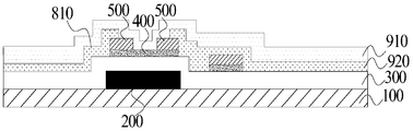
- Figure 3b is a schematic cross-sectional view taken along line CC' of Figure 3a;
- Figure 3c is a schematic cross-sectional view along line EE' in Figure 3a;
- FIG. 4a is a top plan view of an array substrate according to another embodiment of the present disclosure.
- Figure 4b is a schematic cross-sectional view taken along line CC' of Figure 4a;
- Figure 4c is a schematic cross-sectional view along line EE' in Figure 4a;
- FIG. 5a is a schematic top plan view of an array substrate according to another embodiment of the present disclosure.
- Figure 5b is a schematic cross-sectional view taken along line CC' of Figure 5a;
- Figure 5c is a schematic cross-sectional view along line EE' in Figure 5a;
- 6a is a schematic top plan view of an array substrate according to another embodiment of the present disclosure.
- Figure 6b is a schematic cross-sectional view along line BB' in Figure 6a;
- Figure 6c is a schematic cross-sectional view taken along line CC' of Figure 6a;
- Figure 6d is a schematic view showing the structure of the U-shaped cross section along the line DD' in Figure 6a;
- FIG. 7a is a top plan view of an array substrate according to another embodiment of the present disclosure.
- Figure 7b is a schematic cross-sectional view along line BB' in Figure 7a;
- Figure 7c is a schematic cross-sectional view taken along line CC' of Figure 7a;
- Figure 7d is a schematic view showing the structure of the U-shaped cross section taken along the line DD' in Figure 7a;
- FIG. 8a is a top plan view of an array substrate according to another embodiment of the present disclosure.
- Figure 8b is a schematic cross-sectional view taken along line BB' of Figure 8a;
- Figure 8c is a schematic cross-sectional view taken along line CC' of Figure 8a;
- Figure 8d is a schematic view showing the structure of the U-shaped cross section along the DD' line in Figure 8a;
- FIG. 9 is a schematic flow chart of a method of preparing an array substrate according to an embodiment of the present disclosure.
- FIG. 10 is a schematic flow chart of a method of preparing an array substrate according to another embodiment of the present disclosure.
- the source, drain and active layers are formed by the same halftone mask (HTM MASK), an active layer is formed under the source and the drain, for example, referring to FIGS. 1a to 1d and 2.
- the active layer under the source and the drain may be formed to extend beyond the region where the gate is located.
- the illumination hv is performed, referring to FIG. 2, the characteristics of the active layer 400 outside the gate 200 may change, and the holes at the source 501 increase with illumination, resulting in an increase in leakage current of the thin film transistor (TFT).
- TFT thin film transistor
- the switching characteristics of the TFT are affected, and the voltage of the drain is close to the voltage of the source, so that the display is abnormal.
- the inventors of the present application found during the research that in order to improve the above-mentioned increase in TFT leakage current caused by the use of HTM MASK to prepare a display panel, two sets of masks may be used to form the source, drain and active layers, respectively. This can effectively solve the problem of leakage current, but it will increase the cost of production.
- the source or the drain is overlapped with the data line by the connection electrode at the climbing position of the source at the channel with respect to the gate.
- the active layer is not extended beyond the area where the gate is located, and the leakage current generated by the TFT when exposed to light can be reduced without increasing the manufacturing cost.
- embodiments of the present disclosure provide an array substrate having low fabrication cost, reduced leakage current generated by extending an active layer to a gate, and higher display quality, a method of fabricating the same, and a display panel including the same .
- an array substrate is provided.
- the array substrate of the embodiment of the present disclosure will be described in detail with reference to FIGS. 3a to 8d.
- the array substrate includes: a base substrate 100, a thin film transistor, a data line 700, and a connection electrode 800; wherein the thin film transistor is disposed on one side of the base substrate 100, and the data line 700 is disposed on the base substrate 100 On the same side; referring to FIG. 3b, the thin film transistor includes a gate electrode 200, a gate insulating layer 300, an active layer 400, a first electrode, and a second electrode.
- the first electrode and the second electrode are respectively a source and a drain, which are collectively referred to herein as a source and drain 500 for convenience of description. Referring to FIG.
- the orthographic projection of the active layer 400 at the base substrate 100 is within the orthographic projection of the gate 200 under the substrate 100; referring to FIG. 3b, the connection electrode 800
- the source and drain electrodes 500 are electrically connected to the data line 700.
- the inventors have found through long-term research that with reference to the FFS pixel design in the related art of FIG. 3a and FIG. 3b, the source and drain electrodes 500 are connected by the connection electrode 800 at the climbing position of the source and drain electrodes 500 and the gate 200 at the channel.
- the data line 700 is overlapped so that the active layer 400 does not leak outside the gate 200, and the leakage current generated by the TFT under illumination can be reduced without increasing the manufacturing cost.
- connection electrode 800 is not particularly limited as long as the connection electrode 800 composed of the material of this kind has a conductive effect and does not generate a leakage current, and those skilled in the art can according to the array substrate. Use the design to make a choice.
- the connection electrode 800 may be formed of an ITO material.
- the connection electrode 800 of the above material can not only electrically connect the source and drain electrodes 500 to the data line 700, but also further avoid leakage current itself under illumination.
- connection electrode 800 is not particularly limited, as long as the connection electrode 800 fabricated by the method can realize the electrical connection between the source and drain electrodes 500 and the data line 700, those skilled in the art can The specific location of the connection electrode 800 is designed.
- the connection electrode 800 may be an integrated structure formed by a one-time patterning method with a pixel electrode of a thin film transistor. Thus, the connection between the source drain 500 and the connection electrode 800 of the data line 700 is formed without additional manufacturing cost.
- the specific location of the data line 700 is not particularly limited, and those skilled in the art can design according to the use requirements of the array substrate.
- the data line 700 and the source and drain electrodes 500 may be disposed in the same layer.
- the data line 700 and the source and drain electrodes 500 can be formed by one patterning process without increasing the cost of fabricating the array substrate.
- all “same layer setting” in this document refers to being formed by one patterning process or set in the same layer structure.
- not only the data line 700 and the source and drain electrodes 500 may be disposed in the same layer, but the semiconductor layer of the lower surface of the data line 700 and the active layer 400 may also be disposed in the same layer, and thus, the data The line 700, the source/drain electrode 500, and the active layer 400 can be fabricated through the same mask, thereby contributing to reduction in manufacturing cost, and insulating between the source and the drain constituting the source/drain electrode 500, and the source and the drain
- the poles are respectively connected to different structures in which one of the source and the drain is connected to the data line 700, and the other of the source and the drain is connected to the pixel electrode.
- the data line 700 and the gate 200 may be disposed in the same layer.
- the data line 700 and the gate electrode 200 can be formed by one patterning process, and the thickness of the gate insulating layer 300 on the side of the data line 700 away from the substrate 100 can also be increased, thereby reducing parasitic capacitance.
- connection electrode 800 may further include a first sub-connection electrode 810 and a second sub-connection electrode 820.
- the first sub-connection electrode 810 is disposed in the same layer as the pixel electrode and electrically connected to the source and drain electrodes 500; and the second sub-connection electrode 820 is disposed in the same layer as the common electrode, and is connected to the first sub-connection electrode 810 and the data line 700. Electrical connection.
- the source and drain electrodes 500 and the data line 700 can be electrically connected through the first sub-connection electrode 810 and the second sub-connection electrode 820, and the first sub-connection electrode 810 is disposed in the same layer as the pixel electrode, and the second sub-connection electrode 820 is disposed. Setting it in the same layer as the common electrode does not increase the cost of production.
- the connection electrode 800 can also directly connect the source and drain electrodes 500 to the data line 700. Thus, the process of making only one connection electrode 800 is simpler and the manufacturing cost is lower.
- the data line 700 may further include a first data line 710 and a second data line 720.
- the first data line 710 is disposed in the same layer as the source and drain electrodes 500; the second data line 720 is disposed in the same layer as the gate electrode 200, and the second data line 720 and the first data line 710 are electrically connected through the connection electrode.
- the resistance can be reduced by the double data lines 710 and 720 arranged in parallel and in parallel.
- the connection electrode 800 may include a third sub-connection electrode 830 and a fourth sub-connection electrode 840; wherein the third sub-connection electrode 830 and the pixel The electrodes are disposed in the same layer and electrically connected to the source and drain electrodes 500.
- the fourth sub-connection electrode 840 is disposed in the same layer as the common electrode, and is electrically connected to the third sub-connection electrode 830, the first data line 710, and the second data line 720. .
- the first data line 710 and the second data line 720 can be directly connected through the fourth sub-connection electrode 840, thereby achieving parallel connection between the two data lines, thereby reducing the resistance.
- the source and drain electrodes 500 and the first data line 710 and the second data line 720 can be electrically connected through the third sub-connection electrode 830 and the fourth sub-connection electrode 840, and the third sub-connection electrode 830 is in the same layer as the pixel electrode.
- the fourth sub-connection electrode 840 is disposed in the same layer as the common electrode, so that the manufacturing cost is not increased.
- the array substrate may further include an interlayer insulating layer 910, a common electrode 930, and a pixel electrode 920.
- FIG. 3b, FIG. 4b, and FIG. 5b are schematic cross-sectional structures of the array substrate along the CC′ line, and a schematic structural view of the array substrate (including FIG. 3a, FIG. 4a, FIG. 5a, FIG. 6a, and FIG. 7a).
- the base substrate, the gate insulating layer, and the interlayer insulating layer are omitted in FIG. 8a).
- the data line 700 and the source and drain electrodes 500 are disposed in the same layer, and the connection electrode 800 electrically connects the source and drain electrodes 500 with the data line 700; and, the connection electrode 800 and the pixel
- the electrode 920 is disposed in the same layer, the interlayer insulating layer 910 covers the source and drain electrodes 500, the connection electrode 800, and the data line 700, and the common electrode 930 covers at least a portion of the interlayer insulating layer 910.
- connection electrode 800 in this embodiment may include two portions that are at least insulated from each other, the connection electrode 800 of the first portion functions to electrically connect the source and the data line 700, and the connection electrode 800 of the other portion connects the drain and the pixel.
- the electrode 920 is electrically connected and the connecting electrode 800 of the portion may be integrally formed with the pixel electrode 920.
- the data line 700 and the gate 200 are disposed in the same layer, and the first sub-connection electrode 810 and the second sub-connection electrode 820 connect the source and drain electrodes 500 and the data line 700.
- the total thickness of the insulating layer between the data line 700 and the pixel electrode 920 (not shown) in the scheme is increased, so that the parasitic capacitance can be effectively reduced.
- the first data line 710 and the source and drain electrodes 500 are disposed in the same layer
- the second data line 720 and the gate electrode 200 are disposed in the same layer
- the fourth sub-connection electrode 840 electrically connects the source and drain electrodes 500 to the first data line 710 and the second data line 720
- the third sub-connection electrode 830 and the pixel electrode 920 are disposed in the same layer
- the fourth sub-connection electrode 840 and The common electrode 930 is disposed in the same layer, and the interlayer insulating layer 910 covers the source and drain electrodes 500, the third sub-connection electrode 830, and the first data line 710.
- the dual data lines 710 and 720 in this scheme can collectively conduct current, thereby reducing the resistance.
- an array substrate in which the projection of the active layer on the gate insulating layer falls within the projection of the gate in the gate insulating layer, and the source is connected by the connection electrode.
- the connection with the data line reduces the leakage of light generated by the outer layer of the active layer outside the gate, thereby improving the display stability of the display panel composed of the array substrate.
- a method of making an array substrate is presented.
- a method of fabricating an embodiment of the present disclosure will be described in detail with reference to FIGS. 9 to 10. According to an embodiment of the present disclosure, referring to FIG. 9, the method includes:
- a thin film transistor is fabricated on one side of the base substrate 100; wherein the thin film transistor may include a gate electrode 200, a gate insulating layer 300, an active layer 400, and a source and drain electrode 500.
- the step of forming a thin film transistor may further include S110 and S120, and steps S110 and S120 are respectively described below:
- S110 sequentially forming a gate electrode and a gate insulating layer on one side of the base substrate.
- the gate electrode 200 may be formed on one side of the base substrate 100, and the gate insulating layer 300 may be formed on the side of the gate electrode 200 away from the base substrate 100 and the same side of the base substrate 100.
- a specific method of forming the gate electrode 200 and the gate insulating layer 300 is not particularly limited, and a method of forming a gate electrode and a gate insulating layer which are commonly used in the art may be used, and those skilled in the art may The situation is selected and will not be described here.
- S120 forming an active layer and a source and a drain on a side of the gate insulating layer away from the gate.
- the active layer 400 having the same pattern, the source and drain electrodes 500 may be formed through the same mask; wherein the active layer 400 is formed in the lining
- the projection of the base substrate 100 falls within the projection of the gate 200 within the substrate substrate 100.
- the active layer 400 composed of the photosensitive material is not leaked outside the gate electrode 200, and no leakage current is generated even when exposed to light, thereby reducing the technical problem of display abnormality.
- a specific method of forming the active layer 400 and the source and drain electrodes 500 is not particularly limited, and a method of forming an active layer, a source and a drain of the same pattern, which are commonly used in the art, may be employed, for example, HTM MASK, and the like, those skilled in the art can select according to actual conditions, and details are not described herein again.
- a data line 700 is formed on one side of the base substrate 100.
- the data line 700 may be formed with the gate 200 by one patterning process.
- the total thickness of the insulating layer formed on the surface of the data line 700 is further increased, which is advantageous for reducing the parasitic capacitance, and is formed by using a mask together with the gate 200 without increasing the manufacturing cost of the array substrate.
- a gate insulating layer 300 is formed on the side of the gate electrode 200 and the data line 700 remote from the substrate 100 and the same side of the substrate 100.
- the data line 700 may also be formed by a patterning process with the source and drain electrodes 500 and the active layer 400.
- the connection electrode 800 can electrically connect the data line 700 and the source and drain electrodes 500, and is formed by using a mask together with the source and drain electrodes 500 and the active layer 400 without increasing the manufacturing cost of the array substrate. .
- the data line 700 may include a first data line 710 and a second data line 720, wherein the second data line 720 is formed with the gate 200 by one patterning process.
- the design of the double data line can reduce the resistance, and the second data line 720 and the gate 200 are jointly formed by using one mask, and the manufacturing cost of the array substrate is not increased.
- a gate insulating layer 300 is formed on the side of the gate 200 and the second data line 720 remote from the substrate 100 and the same side of the substrate 100.
- the data line 700 may include a first data line 710 and a second data line 720, wherein the first data line 710 may be patterned once with the source and drain electrodes 500 and the active layer 400. Process formation. In this way, the design of the double data line can reduce the resistance, and the first data line 710 is fabricated by using a mask together with the source and drain electrodes 500 and the active layer 400, and the manufacturing cost of the array substrate is not increased.
- the source drain 500, the gate insulating layer 300, and the data line are away from the base substrate 100.
- One side forms a connection electrode; wherein the connection electrode is used to electrically connect the source and drain electrodes 500 to the data line.
- connection electrode is not particularly limited, and a method of forming an electrode commonly used in the art, such as a method of forming an ITO layer, etc., can be performed by a person skilled in the art according to actual conditions. Choice, no longer repeat here.
- connection electrode 800 may be formed on the side, and thus, the connection electrode 800 may electrically connect the data line 700 disposed in the same layer to the source and drain electrodes 500.
- the first side of the source and drain electrodes 500 and the gate insulating layer 300 away from the substrate substrate 100 is formed.
- the sub-electrode 810 is connected, and the first sub-connection electrode 810 may be formed by a patterning process with the pixel electrode for electrical connection with the source and drain electrodes 500; then, the first sub-connection electrode 810 and the data line 700 are further away from the substrate.
- One side of the substrate 100 forms a second sub-connection electrode 820, and the second sub-connection electrode 820 may be formed with the common electrode by one patterning process for electrically connecting with the first sub-connection electrode 810 and the data line 700.
- the data line 700 is not disposed in the same layer as the source and drain electrodes 500, it can be electrically connected through the first sub-connection electrode 810 and the second sub-connection electrode 820.
- the source and drain electrodes 500 and the side of the gate insulating layer 300 away from the base substrate 100 are formed.
- the third sub-connection electrode 830, and the third sub-connection electrode 830 may be formed by a patterning process with the pixel electrode for electrical connection with the source and drain electrodes 500; then, at the third sub-connection electrode 830, the first data line 710 And a fourth sub-connection electrode 840 is formed on a side of the second data line 720 away from the base substrate 100, and the fourth sub-connection electrode 840 can be formed with the common electrode by one patterning process for separately from the third sub-connection electrode 810 It is electrically connected to the first data line 710 and the second data line 720.
- the source and drain electrodes 500 can be electrically connected thereto through the third sub-connection electrode 830 and the fourth sub-connection electrode 840.
- a fabrication method which provides an array substrate that uses a connection electrode to connect a source and a data line, thereby reducing leakage of the active layer under the source at the gate.
- the external light leakage problem which in turn increases the display stability of the display composed of the array substrate, does not increase the number of MASKs and the cost of manufacturing the array substrate.
- the display panel includes the above array substrate.
- the specific type of the display panel is not particularly limited, and various types of display panels commonly used in the art may be used, such as a television, a mobile phone, a computer display, a flat panel display, a game machine, and a wearable device. And the living room, the home appliance, and the like having the display panel, and those skilled in the art can select according to the actual use requirements of the display panel, and details are not described herein again.
- the display panel includes other necessary components and components, such as a liquid crystal display, such as a color film substrate, a liquid crystal display layer, a light source assembly, a control component, a circuit, and a housing, etc.
- a liquid crystal display such as a color film substrate, a liquid crystal display layer, a light source assembly, a control component, a circuit, and a housing, etc.
- the person skilled in the art can supplement according to the specific type of the array substrate, and details are not described herein again.
- a display panel wherein the array substrate solves the problem of light leakage caused by the leakage of the active layer outside the gate, thereby improving the display stability of the display panel. And its manufacturing costs will not increase.
- connection may be disassembled or integrated; it may be a mechanical connection or an electrical connection; it may be a direct connection or an indirect connection through an intermediate medium, which may be the internal communication of the two elements or the interaction of the two elements.
- the specific meanings of the above terms in the present disclosure can be understood by those skilled in the art on a case-by-case basis.
- first”, “second”, “third”, “fourth” are used for descriptive purposes only and are not to be construed as indicating or implying a relative importance or implicitly indicating the number of technical features indicated.
- features defining “first”, “second”, “third”, “fourth” may include at least one of the features, either explicitly or implicitly.
- the meaning of "a plurality” is at least two, such as two, three, etc., unless specifically defined otherwise.
Landscapes
- Physics & Mathematics (AREA)
- Nonlinear Science (AREA)
- Engineering & Computer Science (AREA)
- Microelectronics & Electronic Packaging (AREA)
- Mathematical Physics (AREA)
- Chemical & Material Sciences (AREA)
- Crystallography & Structural Chemistry (AREA)
- General Physics & Mathematics (AREA)
- Optics & Photonics (AREA)
- Liquid Crystal (AREA)
- Devices For Indicating Variable Information By Combining Individual Elements (AREA)
Abstract
一种阵列基板、其制备方法和显示面板,阵列基板包括:衬底基板(100);薄膜晶体管,设置在衬底基板(100)的一侧,并包括第一电极、第二电极和栅极(200);数据线(700),设置在衬底基板(100)的一侧;连接电极(800),将薄膜晶体管的第一电极与数据线(700)电连接;其中,薄膜晶体管的有源层(400)在衬底基板(100)上的正投影位于薄膜晶体管的栅极(200)在衬底基板(100)的正投影之内。阵列基板,其有源层(400)在栅绝缘层(300)的投影都落在栅极(200)在栅绝缘层(300)的投影之内,再利用连接电极(800)将第一电极和数据线(700)连接,从而减少了有源层(400)外漏在栅极(200)之外而产生的光漏电问题,进而提高阵列基板组成的显示面板的显示稳定性。
Description
交叉引用
本申请要求于2017年7月3日提交的申请号为201710534097.8、名称为“阵列基板及其制备方法、显示装置”的中国专利申请的优先权,该中国专利申请的全部内容通过引用全部并入本文。
本公开涉及显示技术领域,具体的,涉及阵列基板、其制备方法和显示面板。
在像素设计中,为了节约成本,一般会尽量减少所使用的掩膜(Mask)的数量。例如,目前广泛采用的方法是,用同一半色调掩膜(HTM MASK)来形成源极、漏极和有源层以减少掩膜的数量。
但是,这种方法通常会导致薄膜晶体管(TFT)的漏电流增加,而使TFT的性能劣化。因此,当前阵列基板的制造方法仍需改进。
发明内容
本公开的实施例涉及一种阵列基本、其制备方法和显示面板。
在本公开的第一方面,提出了一种阵列基板。
根据本公开的实施例,所述阵列基板包括:衬底基板;薄膜晶体管,所述薄膜晶体管设置在所述衬底基板的一侧,并包括第一电极、第二电极和栅极;数据线,所述数据线设置在所述衬底基板的所述一侧;连接电极,所述连接电极将所述薄膜晶体管的第一电极与所述数据线电连接;其中,所述薄膜晶体管的有源层在所述衬底基板上的正投影位于所述薄膜晶体管的栅极在所述衬底基板的正投影之内。
根据本公开的实施例,所述连接电极由ITO材料形成。
根据本公开的实施例,所述数据线与所述第一电极、第二电极同层设置。
根据本公开的实施例,所述数据线与所述栅极同层设置。
根据本公开的实施例,所述连接电极包括:第一子连接电极,所述第一子连接电极与像素电极同层设置,且与所述第一电极电连接;第二子连接电极,所述第二子连接电极与公共电极同层设置,且与所述第一子连接电极、所述数据线电连接。
根据本公开的实施例,所述数据线包括:第一数据线,与所述第一电极、所述第二电极同层设置;第二数据线,与所述栅极同层设置,且所述第二数据线与所述第一数据线通过所述连接电极电连接。
根据本公开的实施例,所述连接电极包括:第三子连接电极,所述第三子连接电极与像素电极同层设置,且与所述第一电极电连接;第四子连接电极,所述第四子连接电极与公共电极同层设置,且与所述第三子连接电极、所述第一数据线、所述第二数据线电连接。
在本公开的第二方面,提出了一种阵列基板的制备方法。
根据本公开的实施例,所述方法包括:在衬底基板的一侧,形成薄膜晶体管,其中,所述薄膜晶体管包括第一电极、第二电极和栅极,并且所述薄膜晶体管的有源层在所述衬底基板的正投影位于所述栅极在所述衬底基板的正投影之内;在衬底基板的一所述侧,形成数据线;在所述薄膜晶体管的第一电极和所述数据线的远离所述衬底基板的一侧形成连接电极,其中,所述连接电极将所述第一电极与数据线电连接。
根据本公开的实施例,通过一次构图工艺形成所述数据线与所述第一电极、所述第二电极、所述有源层。
根据本公开的实施例,通过一次构图工艺形成所述数据线与所述栅极;通过一次构图工艺形成所述第一电极、第二电极和有源层。
根据本公开的实施例,所述连接电极包括第一子连接电极和第二子连接电极;其中,所述第一子连接电极与像素电极通过一次构图工艺形成,用于与所述第一电极电连接;所述第二子连接电极与公共电极通过一次构图工艺形成,用于与所述第一子连接电极、所述数据线电连接。
根据本公开的实施例,所述数据线包括第一数据线和第二数据线,其中,所述第一数据线与所述第一电极、所述第二电极、所述有源层极通过一次构图工艺形成,所述第二数据线与所述栅极通过一次构图工艺形成。
根据本公开的实施例,所述连接电极包括第三子连接电极和第四子连接电极;其中,所述第三子连接电极与像素电极通过一次构图工艺形成,用于与所述第一电极电连接;所述第四子连接电极与公共电极通过一次构图工艺形成,用于与所述第三子连接电极、所述第一数据线、所述第二数据线电连接。
在本公开的第三方面,提出了一种显示面板。
根据本公开的实施例,所述显示面板包括上述的阵列基板。
本公开的附加方面和优点将在下面的描述中部分给出,部分将从下面的描述中变得明显,或通过本公开的实践了解到。
本公开的上述和/或附加的方面和优点从结合下面附图对实施例的描述中将变得明显和容易理解,其中:
图1a是一种阵列基板的俯视结构示意图;
图1b是图1a中沿BB’线的截面结构示意图;
图1c是图1a中沿CC’线的截面结构示意图;
图1d是图1a中沿DD’线的U型截面展开后的结构示意图;
图2是示出图1a中的阵列基板的TFT产生漏电流的原理示意图;
图3a是本公开的实施例的阵列基板的俯视结构示意图;
图3b是图3a中沿CC’线的截面结构示意图;
图3c是图3a中沿EE’线的截面结构示意图;
图4a是本公开的另一实施例的阵列基板的俯视结构示意图;
图4b是图4a中沿CC’线的截面结构示意图;
图4c是图4a中沿EE’线的截面结构示意图;
图5a是本公开的另一实施例的阵列基板的俯视结构示意图;
图5b是图5a中沿CC’线的截面结构示意图;
图5c是图5a中沿EE’线的截面结构示意图;
图6a是本公开的另一实施例的阵列基板的俯视结构示意图;
图6b是图6a中沿BB’线的截面结构示意图;
图6c是图6a中沿CC’线的截面结构示意图;
图6d是图6a中沿DD’线的U型截面展开后的结构示意图;
图7a是本公开的另一实施例的阵列基板的俯视结构示意图;
图7b是图7a中沿BB’线的截面结构示意图;
图7c是图7a中沿CC’线的截面结构示意图;
图7d是图7a中沿DD’线的U型截面展开后的结构示意图;
图8a是本公开的另一实施例的阵列基板的俯视结构示意图;
图8b是图8a中沿BB’线的截面结构示意图;
图8c是图8a中沿CC’线的截面结构示意图;
图8d是图8a中沿DD’线的U型截面展开后的结构示意图;
图9是本公开的实施例的制备阵列基板方法的流程示意图;
图10是本公开的另一个实施例的制备阵列基板方法的流程示意图。
下面详细描述本公开的实施例,本领域技术人员会理解,下面实施例旨在用于解释本公开,而不应视为对本公开的限制。除非特别说明,在下面实施例中没有明确描述具体技术或条件的,本领域技术人员可以按照本领域内的常用的技术或条件或按照产品说明书进行。所用试剂或仪器未注明生产厂商者,均为可通过市购到的常规产品。
通常,在用同一半色调掩膜(HTM MASK)来形成源极、漏极和有源层时,由于在源极和漏极下会形成有源层,例如,参考图1a~图1d和图2。在这种情况下,特别参照图2所示的三处沟道处(I、II、III),源极和漏极之下的有源层会形成为延伸到栅极所在的区域之外。在进行光照hv时,参考图2,在栅极200之外的有源层400的特性会发生变化,源极501处的空穴随着光照而增加,导致薄膜晶体管(TFT)的漏电流增加,TFT的开关特性受到影响,漏极的电压接近源极的电压而使显示异常。
本申请的发明人在研究过程中发现,为了改善上述的由使用HTM MASK制备显示面板而导致的TFT漏电流的增加,可以分别使用两套掩膜来形成源极、漏极和有源层,这可有效地解决漏电流的问题,但是会增加制作的成本。
本申请人的发明人经过研究进一步发现,基于相关技术的FFS像素设计,在沟道处的源极相对栅极的爬坡位置,用连接电极将源极或漏极与数据线进行搭接,使有源层不会延伸至栅极所在的区域之外,可以在减小在受到光照时TFT产生的漏电流的同时,也不会增加制作的成本。
有鉴于此,本公开的实施例提供了一种制作成本低、减少因有源层延伸至栅极外而产生的漏电流并且显示质量更高的阵列基板、其制备方法以及包括其的显示面板。
在本公开的一个方面,提供了一种阵列基板。参照图3a~8d,对本公开的实施例的阵列基板进行详细的描述。
根据本公开的实施例,阵列基板包括:衬底基板100、薄膜晶体管、数据线700和连接电极800;其中,薄膜晶体管设置在衬底基板100的一侧,数据线700设置在衬底基板100的同一侧;参考图3b,薄膜晶体管包括栅极200、栅绝缘层300、有源层400、第一电极和第二电极。第一电极和第二电极分别为源极和漏极,为了便于描述,这里将其统称为源漏极500。参考图3a(其中省略了衬底基板和栅绝缘层),有源层400在衬底基板100的正投影在栅极200在衬底基板100的正投影之内;参考图3b,连接电极800将源漏极500与数据线700电连接。
发明人经过长期的研究发现,参考图3a和图3b的相关技术中的FFS像素设计,在沟道处的源漏极500与栅极200的爬坡位置,采用连接电极800将源漏极500与数据线700进行搭接,使有源层400不会外漏在栅极200外,可以减小在光照情况下TFT产生的漏电流,同时也不会增加制作的成本。
根据本公开的实施例,连接电极800的具体种类不受特别的限制,只要该种类的材料组成的连接电极800具有导电作用且不会产生漏电流即可,本领域技术人员可根据该阵列基板的使用设计进行选择。在本公开的一些实施例中,连接电极800可以是由ITO材料形成的。如此,采用上述材料的连接电极800,不仅能将源漏极500与数据线700电连接,还可进一步避免光照情况下本身产生漏电流。
根据本公开的实施例,连接电极800的具体制作方法不受特别的限制,只要该方 法制作的连接电极800可实现源漏极500与数据线700的电连接即可,本领域技术人员可根据该连接电极800的具体位置进行设计。在本公开的一些实施例中,连接电极800可以是与薄膜晶体管的像素电极,通过一次构图法形成的一体化结构。如此,形成的连接源漏极500与数据线700的连接电极800,并不会额外增加制造成本。
根据本公开的实施例,数据线700的具体位置不受特别的限制,本领域技术人员可根据该阵列基板的使用要求进行设计。在本公开的一些实施例中,参照图3b,数据线700与源漏极500可以同层设置。如此,数据线700与源漏极500可通过一次构图工艺形成,而不会增加制作该阵列基板的成本。需要说明的是,本文中所有“同层设置”是指通过一次构图工艺形成的,或者设置在同一层结构中。在本公开的一些具体示例中,参考图3b,不仅数据线700与源漏极500可同层设置,而数据线700下表面的半导体层与有源层400也可同层设置,如此,数据线700、源漏电极500和有源层400可通过同一个掩膜制作,从而有利于降低制造成本,并且组成源漏电极500的源极和漏极之间是绝缘的,且源极和漏极分别连接不同的结构,其中,源极和漏极中的一个连接数据线700,而源极和漏极中的另一个连接像素电极。在本公开的另一些实施例中,参照图4b,数据线700与栅极200可以同层设置。如此,数据线700与栅极200可通过一次构图工艺形成,并且还可增加数据线700远离基板100一侧的栅绝缘层300的厚度,从而减小寄生电容。
在本公开的一些实施例中,参照图4b,连接电极800还可以进一步包括第一子连接电极810和第二子连接电极820。其中,第一子连接电极810与像素电极同层设置,且与源漏极500电连接;而第二子连接电极820与公共电极同层设置,且与第一子连接电极810、数据线700电连接。如此,通过第一子连接电极810和第二子连接电极820,可以将源漏极500和数据线700电连接,并且第一子连接电极810与像素电极同层设置、第二子连接电极820与公共电极同层设置,则不会增加制作的成本。在本公开的一些实施例中,连接电极800也可以直接将源漏极500与数据线700电连接,如此,只制作一个连接电极800的工艺更简单、制作成本更低。
根据本公开的实施例,参照图5b,数据线700可进一步包括第一数据线710和第二数据线720。其中,第一数据线710与源漏极500同层设置;而第二数据线720与栅极200同层设置,且第二数据线720与第一数据线710通过连接电极电连接。如此,通过平行设置且并联的双数据线710和720,可使电阻降低。
在本公开的另一些实施例中,参照图5b,连接电极800(图中未标出)可以包括第三子连接电极830和第四子连接电极840;其中,第三子连接电极830与像素电极同层设置,且与源漏极500电连接;而第四子连接电极840与公共电极同层设置,且与第三子连接电极830、第一数据线710、第二数据线720电连接。并且,第一数据线710和第二数据线720之间可通过第四子连接电极840直接连接,从而实现两个数据线之间的并联,进而可减小电阻。如此,通过第三子连接电极830和第四子连接电 极840,可以将源漏极500和第一数据线710、第二数据线720电连接,并且第三子连接电极830与像素电极同层设置、第四子连接电极840与公共电极同层设置,则不会增加制作的成本。
根据本公开的实施例,参考图6a~8d,该阵列基板还可以进一步包括层间绝缘层910、公共电极930和像素电极920。需要说明的是,图3b、图4b和图5b均是阵列基板沿CC’线的截面结构示意图,且该阵列基板的俯视结构示意图(包括图3a、图4a、图5a、图6a、图7a和图8a)中忽略了衬底基板、栅绝缘层和层间绝缘层。
在本公开的一些具体示例中,参考图6a~图6d,数据线700和源漏极500同层设置,连接电极800将源漏极500与数据线700电连接;并且,连接电极800和像素电极920同层设置,层间绝缘层910覆盖源漏极500、连接电极800和数据线700,而公共电极930覆盖层间绝缘层910的至少一部分。如此,该方案中的连接电极800可以包括至少相互绝缘的两部分,第一部分的连接电极800起到将源极与数据线700电连接的作用,而另一部分的连接电极800将漏极与像素电极920电连接且该部分的连接电极800可与像素电极920一体成型。
在本公开的另一些具体示例中,参考图7a~图7d,数据线700和栅极200同层设置,第一子连接电极810和第二子连接电极820将源漏极500与数据线700电连接;并且,第一子连接电极810和像素电极920同层设置,第二子连接电极820和公共电极930同层设置,而层间绝缘层910覆盖源漏极500和第一子连接电极810。如此,该方案中的数据线700和像素电极920(图中未标出)之间的绝缘层总厚度增加,从而可有效地减小寄生电容。
在本公开的另一些具体示例中,参考图8a~图8d,第一数据线710和源漏极500同层设置,第二数据线720和栅极200同层设置,第三子连接电极830和第四子连接电极840将源漏极500与第一数据线710、第二数据线720电连接;并且,第三子连接电极830和像素电极920同层设置,第四子连接电极840和公共电极930同层设置,而层间绝缘层910覆盖源漏极500、第三子连接电极830和第一数据线710。如此,该方案中的双数据线710和720可共同地传导电流,从而减小电阻。
综上所述,根据本公开的实施例,提出了一种阵列基板,其有源层在栅绝缘层的投影都落在栅极在栅绝缘层的投影之内,再利用连接电极将源极和数据线连接,从而减少了有源层外漏在栅极外而产生的光漏电问题,进而提高该阵列基板组成的显示面板的显示稳定性。
在本公开的二个方面,提出了一种制备阵列基板的方法。参照图9~10,对本公开的实施例的制作方法进行详细的描述。根据本公开的实施例,参照图9,该方法包括:
S100:在衬底基板的一侧,形成薄膜晶体管。
在该步骤中,在衬底基板100的一侧制作出薄膜晶体管;其中,薄膜晶体管可包括栅极200、栅绝缘层300、有源层400和源漏极500。根据本公开的实施例,参考图10,形成薄膜晶体管的步骤可进一步包括S110和S120,下面对步骤S110和S120分别进行描述:
S110:在衬底基板的一侧依次形成栅极、栅绝缘层。
在该步骤中,可在衬底基板100的一侧形成栅极200,再在栅极200远离衬底基板100的一侧以及衬底基板100的同侧形成栅绝缘层300。根据本公开的实施例,形成栅极200和栅绝缘层300的具体方法,不受特别的限制,本领域内常用的形成栅极和栅绝缘层的方法均可,本领域技术人员可根据实际情况进行选择,在此不再赘述。
S120:在栅绝缘层远离栅极的一侧,形成有源层、源漏极。
在该步骤中,在栅绝缘层300远离栅极200的一侧,可通过同一掩膜板,形成具有相同图案的有源层400、源漏极500;其中,形成的有源层400在衬底基板100的投影落在栅极200在衬底基板100的投影之内。如此,光敏材料组成的有源层400没有外漏在栅极200外,即使受到光照时也不会产生漏电流,进而减小显示异常的技术问题。
根据本公开的实施例,形成有源层400、源漏极500的具体方法,不受特别的限制,本领域内常用的形成相同图案的有源层、源漏极的方法均可,例如采用HTM MASK,等等,本领域技术人员可根据实际情况进行选择,在此不再赘述。
S200:在衬底基板的一侧,形成数据线。
在该步骤中,在衬底基板100的一侧制作出数据线700。
在本公开的一些实施例中,该数据线700可以是与栅极200通过一次构图工艺形成。如此,后续再在数据线700表面形成的绝缘层总厚度更大,有利于减小寄生电容,并且与栅极200共同采用一个掩膜制作,不会增加该阵列基板的制作成本。而且,在栅极200和数据线700的远离基板100的一侧以及基板100的同侧形成栅绝缘层300。
在本公开的另一些实施例中,该数据线700也可以是与源漏极500、有源层400通过一次构图工艺形成。如此,只需一层连接电极800就可将数据线700和源漏极500电连接,并且与源漏极500、有源层400共同采用一个掩膜制作,不会增加该阵列基板的制作成本。
在本公开的另一些实施例中,该数据线700可包括第一数据线710和第二数据线720,其中的第二数据线720是与栅极200通过一次构图工艺形成。如此,采用双数据线的设计可降低电阻,并且,第二数据线720与栅极200共同采用一个掩膜制作,不会增加该阵列基板的制作成本。而且,在栅极200和第二数据线720的远离基板100的一侧以及基板100的同侧形成栅绝缘层300。
在本公开的另一些实施例中,该数据线700可包括第一数据线710和第二数据线720,其中的第一数据线710可以是与源漏极500、有源层400通过一次构图工艺形 成。如此,采用双数据线的设计可降低电阻,并且,第一数据线710与源漏极500、有源层400共同采用一个掩膜制作,也不会增加该阵列基板的制作成本。
S300:在源漏极、栅绝缘层远离衬底基板的一侧形成连接电极。
在该步骤中,为了解决缩小有源层400的面积而带来的源漏极500与数据线无法导通的问题,所以在源漏极500、栅绝缘层300和数据线远离衬底基板100的一侧形成连接电极;其中,连接电极用于将源漏极500与数据线电连接。
根据本公开的实施例,形成连接电极的具体方法不受特别的限制,本领域内常用的形成电极的方法均可,例如形成ITO层的方法,等等,本领域技术人员可根据实际情况进行选择,在此不再赘述。
在本公开的一些实施例中,在数据线700与源漏极500是通过一次构图工艺形成的情况下,在源漏极500、栅绝缘层300和数据线700的远离衬底基板100的一侧形成连接电极800即可,如此,连接电极800可将同层设置的数据线700与源漏极500电连接。
在本公开的另一些实施例中,在数据线700与栅极200是通过一次构图工艺形成的情况下,在源漏极500和栅绝缘层300的远离衬底基板100的一侧形成第一子连接电极810,并且第一子连接电极810可以与像素电极通过一次构图工艺形成,用于与源漏极500电连接;然后,再在第一子连接电极810和数据线700的远离衬底基板100的一侧形成第二子连接电极820,并且第二子连接电极820可以与公共电极通过一次构图工艺形成,用于与第一子连接电极810、数据线700电连接。如此,即使数据线700与源漏极500不是同层设置,也可以通过第一子连接电极810和第二子连接电极820将其电连接。
在本公开的另一些实施例中,在数据线700包括第一数据线710和第二数据线720的情况下,在源漏极500和栅绝缘层300的远离衬底基板100的一侧形成第三子连接电极830,并且第三子连接电极830可与像素电极通过一次构图工艺形成,用于与源漏极500电连接;然后,再在第三子连接电极830、第一数据线710和第二数据线720的远离衬底基板100的一侧形成第四子连接电极840,并且第四子连接电极840可与公共电极通过一次构图工艺形成,用于与第三子连接电极810分别与第一数据线710、第二数据线720电连接。如此,即使采用双数据线的设计,也可通过第三子连接电极830和第四子连接电极840将源漏极500与其电连接。
综上所述,根据本公开的实施例,提出了一种制作方法,获得的阵列基板,其利用连接电极将源极和数据线连接,从而减少了源极下面有源层外漏在栅极外而产生的光漏电问题,进而提高该阵列基板组成的显示器的显示稳定性,并且该方法也不会增加MASK数目和制造阵列基板的成本。
在本公开的三个方面,提出了一种显示面板。根据本公开的实施例,该显示面板 包括上述的阵列基板。
根据本公开的实施例,该显示面板的具体类型不受特别的限制,本领域内常用的显示面板的类型均可,具体例如电视、手机、电脑显示屏、平板显示器、游戏机、可穿戴设备及具有显示面板的生活、家用电器等等,本领域技术人员可根据该显示面板的实际使用要求进行选择,在此不再赘述。
需要说明的是,该显示面板除了阵列基板以外,还包括其他必要的组件和构成,以液晶显示器为例,具体例如彩膜基板、液晶显示层、光源组件、控制组件、电路和外壳,等等,,本领域技术人员可根据该阵列基板的具体类型进行补充,在此不再赘述。
综上所述,根据本公开的实施例,提出了一种显示面板,其阵列基板解决了有源层外漏在栅极外而产生的光漏电问题,进而提高该显示面板的显示稳定性,并且其制造成本也不会增加。本领域技术人员能够理解的是,前面针对阵列基板所描述的特征和优点,仍适用于该显示面板,在此不再赘述。
在本公开的描述中,需要理解的是,术语“中心”、“纵向”、“横向”、“长度”、“宽度”、“厚度”、“上”、“下”、“前”、“后”、“左”、“右”、“竖直”、“水平”、“顶”、“底”、“内”、“外”、“顺时针”、“逆时针”、“轴向”、“径向”、“周向”等指示的方位或位置关系为基于附图所示的方位或位置关系,仅是为了便于描述本公开和简化描述,而不是指示或暗示所指的装置或元件必须具有特定的方位、以特定的方位构造和操作,因此不能理解为对本公开的限制。
在本公开的描述中,除非另有明确的规定和限定,术语“安装”、“相连”、“连接”、“固定”等术语应做广义理解,例如,可以是固定连接,也可以是可拆卸连接,或成一体;可以是机械连接,也可以是电连接;可以是直接连接,也可以通过中间媒介间接连接,可以是两个元件内部的连通或两个元件的相互作用关系。对于本领域的普通技术人员而言,可以根据具体情况理解上述术语在本公开中的具体含义。
此外,术语“第一”、“第二”、“第三”、“第四”仅用于描述目的,而不能理解为指示或暗示相对重要性或者隐含指明所指示的技术特征的数量。由此,限定有“第一”、“第二”、“第三”、“第四”的特征可以明示或者隐含地包括至少一个该特征。在本公开的描述中,“多个”的含义是至少两个,例如两个,三个等,除非另有明确具体的限定。
在本说明书的描述中,参考术语“一个实施例”、“一些实施例”、“示例”、“具体示例”、或“一些示例”等的描述意指结合该实施例或示例描述的具体特征、结构、材料或者特点包含于本公开的至少一个实施例或示例中。在本说明书中,对上述术语的示意性表述不必须针对的是相同的实施例或示例。而且,描述的具体特征、结构、材料或者特点可以在任一个或多个实施例或示例中以合适的方式结合。此外,在不相互矛盾的情况下,本领域的技术人员可以将本说明书中描述的不同实施例或示例以及不 同实施例或示例的特征进行结合和组合。
尽管上面已经示出和描述了本公开的实施例,可以理解的是,上述实施例是示例性的,不能理解为对本公开的限制,本领域的普通技术人员在本公开的范围内可以对上述实施例进行变化、修改、替换和变型。
Claims (14)
- 一种阵列基板,包括:衬底基板;薄膜晶体管,设置在所述衬底基板的一侧,并包括第一电极、第二电极和栅极;数据线,设置在所述衬底基板的所述一侧;连接电极,将所述薄膜晶体管的第一电极与所述数据线电连接;其中,所述薄膜晶体管的有源层在所述衬底基板上的正投影位于所述薄膜晶体管的栅极在所述衬底基板的正投影之内。
- 根据权利要求1所述的阵列基板,其中,所述连接电极由ITO材料形成。
- 根据权利要求1所述的阵列基板,其中,所述数据线与所述第一电极、所述第二电极同层设置。
- 根据权利要求1所述的阵列基板,其中,所述数据线与所述栅极同层设置。
- 根据权利要求4所述的阵列基板,其中,所述连接电极包括:第一子连接电极,与像素电极同层设置,且与所述第一电极电连接;第二子连接电极,与公共电极同层设置,且与所述第一子连接电极、所述数据线电连接。
- 根据权利要求1所述的阵列基板,其中,所述数据线包括:第一数据线,与所述第一电极、所述第二电极同层设置;第二数据线,与所述栅极同层设置,且与所述第一数据线通过所述连接电极电连接。
- 根据权利要求6所述的阵列基板,其中,所述连接电极包括:第三子连接电极,与像素电极同层设置,且与所述第一电极电连接;第四子连接电极,与公共电极同层设置,且与所述第三子连接电极、所述第一数据线、所述第二数据线电连接。
- 一种阵列基板的制备方法,包括:在衬底基板的一侧,形成薄膜晶体管,其中,所述薄膜晶体管包括第一电极、第二电极和栅极,并且所述薄膜晶体管的有源层在所述衬底基板的正投影位于所述薄膜晶体管的栅极在所述衬底基板的正投影之内;在衬底基板的所述一侧,形成数据线;在所述薄膜晶体管的第一电极和所述数据线远离所述衬底基板的一侧,形成连接电极,其中,所述连接电极将所述第一电极与数据线电连接。
- 根据权利要求8所述的制备方法,其中,通过一次构图工艺形成所述数据线与所述第一电极、所述第二电极、所述有源层。
- 根据权利要求8所述的制备方法,其中,通过一次构图工艺形成所述数据线与所述栅极;通过一次构图工艺形成所述第一电极、所述第二电极和有源层。
- 根据权利要求10所述的制备方法,其中,所述连接电极包括第一子连接电极和第二子连接电极;其中,所述第一子连接电极与像素电极通过一次构图工艺形成,用于与所述第一电极电连接;所述第二子连接电极与公共电极通过一次构图工艺形成,用于与所述第一子连接电极、所述数据线电连接。
- 根据权利要求8所述的制备方法,其中,所述数据线包括第一数据线和第二数据线,其中,所述第一数据线与所述第一电极、所述第二电极、所述有源层通过一次构图工艺形成,所述第二数据线与所述栅极通过一次构图工艺形成。
- 根据权利要求12所述的制备方法,其中,所述连接电极包括第三子连接电极和第四子连接电极;其中,所述第三子连接电极与像素电极通过一次构图工艺形成,用于与所述第一电极电连接;所述第四子连接电极与公共电极通过一次构图工艺形成,用于与所述第三子连接电极、所述第一数据线、所述第二数据线电连接。
- 一种显示面板,包括权利要求1-7任一项所述的阵列基板。
Priority Applications (1)
| Application Number | Priority Date | Filing Date | Title |
|---|---|---|---|
| US16/309,082 US11315956B2 (en) | 2017-07-03 | 2018-04-20 | Array substrate, manufacturing method thereof and display panel |
Applications Claiming Priority (2)
| Application Number | Priority Date | Filing Date | Title |
|---|---|---|---|
| CN201710534097.8 | 2017-07-03 | ||
| CN201710534097.8A CN107134463B (zh) | 2017-07-03 | 2017-07-03 | 阵列基板及其制备方法、显示面板 |
Publications (1)
| Publication Number | Publication Date |
|---|---|
| WO2019007136A1 true WO2019007136A1 (zh) | 2019-01-10 |
Family
ID=59736645
Family Applications (1)
| Application Number | Title | Priority Date | Filing Date |
|---|---|---|---|
| PCT/CN2018/083983 Ceased WO2019007136A1 (zh) | 2017-07-03 | 2018-04-20 | 阵列基板、其制备方法和显示面板 |
Country Status (3)
| Country | Link |
|---|---|
| US (1) | US11315956B2 (zh) |
| CN (1) | CN107134463B (zh) |
| WO (1) | WO2019007136A1 (zh) |
Families Citing this family (7)
| Publication number | Priority date | Publication date | Assignee | Title |
|---|---|---|---|---|
| CN107134463B (zh) | 2017-07-03 | 2020-02-21 | 京东方科技集团股份有限公司 | 阵列基板及其制备方法、显示面板 |
| CN108897445B (zh) * | 2018-05-15 | 2024-05-24 | 京东方科技集团股份有限公司 | 触控显示装置、触控显示面板及其制造方法 |
| US11049884B2 (en) * | 2019-04-28 | 2021-06-29 | Wuhan China Star Optoelectronics Semiconductor Display Technology Co., Ltd. | Display panel and method of manufacturing same, and display module |
| CN113376904A (zh) * | 2020-03-10 | 2021-09-10 | 成都京东方光电科技有限公司 | 一种单色液晶显示面板以及双层液晶显示装置 |
| GB2609826A (en) | 2021-03-01 | 2023-02-15 | Boe Technology Group Co Ltd | Display panel and display device |
| CN119156710A (zh) * | 2023-04-17 | 2024-12-17 | 京东方科技集团股份有限公司 | 阵列基板和显示装置 |
| WO2025111892A1 (zh) * | 2023-11-29 | 2025-06-05 | 京东方科技集团股份有限公司 | 阵列基板及其制备方法、显示装置 |
Citations (3)
| Publication number | Priority date | Publication date | Assignee | Title |
|---|---|---|---|---|
| US20160293771A1 (en) * | 2014-08-19 | 2016-10-06 | Boe Technology Group Co., Ltd. | Thin film transistor and its manufacturing method, array substrate and its manufacturing method, and display device |
| CN106252217A (zh) * | 2016-08-25 | 2016-12-21 | 京东方科技集团股份有限公司 | 薄膜晶体管及其制备方法、阵列基板和显示装置 |
| CN107134463A (zh) * | 2017-07-03 | 2017-09-05 | 京东方科技集团股份有限公司 | 阵列基板及其制备方法、显示面板 |
Family Cites Families (3)
| Publication number | Priority date | Publication date | Assignee | Title |
|---|---|---|---|---|
| CN104332473A (zh) * | 2014-08-29 | 2015-02-04 | 京东方科技集团股份有限公司 | 一种阵列基板、其制备方法、显示面板和显示装置 |
| CN104810321A (zh) * | 2015-04-30 | 2015-07-29 | 京东方科技集团股份有限公司 | 一种tft阵列基板及显示装置的制备方法 |
| KR102618961B1 (ko) * | 2016-09-30 | 2024-01-02 | 삼성디스플레이 주식회사 | 트랜지스터 기판, 표시 장치, 및 트랜지스터 기판 제조 방법 |
-
2017
- 2017-07-03 CN CN201710534097.8A patent/CN107134463B/zh not_active Expired - Fee Related
-
2018
- 2018-04-20 US US16/309,082 patent/US11315956B2/en active Active
- 2018-04-20 WO PCT/CN2018/083983 patent/WO2019007136A1/zh not_active Ceased
Patent Citations (3)
| Publication number | Priority date | Publication date | Assignee | Title |
|---|---|---|---|---|
| US20160293771A1 (en) * | 2014-08-19 | 2016-10-06 | Boe Technology Group Co., Ltd. | Thin film transistor and its manufacturing method, array substrate and its manufacturing method, and display device |
| CN106252217A (zh) * | 2016-08-25 | 2016-12-21 | 京东方科技集团股份有限公司 | 薄膜晶体管及其制备方法、阵列基板和显示装置 |
| CN107134463A (zh) * | 2017-07-03 | 2017-09-05 | 京东方科技集团股份有限公司 | 阵列基板及其制备方法、显示面板 |
Also Published As
| Publication number | Publication date |
|---|---|
| US11315956B2 (en) | 2022-04-26 |
| CN107134463B (zh) | 2020-02-21 |
| CN107134463A (zh) | 2017-09-05 |
| US20210013232A1 (en) | 2021-01-14 |
Similar Documents
| Publication | Publication Date | Title |
|---|---|---|
| WO2019007136A1 (zh) | 阵列基板、其制备方法和显示面板 | |
| CN110459572B (zh) | 显示面板 | |
| CN109658824B (zh) | 显示面板和显示装置 | |
| US8350792B2 (en) | Display device | |
| US10818696B2 (en) | Display panel and fabricating method thereof | |
| CN110828535B (zh) | 一种阵列基板、显示面板和显示装置 | |
| JP2020529640A (ja) | タッチ制御表示パネル | |
| WO2016029564A1 (zh) | 阵列基板及其制备方法、显示面板和显示装置 | |
| WO2015003453A1 (zh) | 显示面板及其制作方法和显示装置 | |
| WO2017214971A1 (en) | Touch display substrate, touch display apparatus having the same, pixel arrangement, and fabricating method thereof | |
| CN104950535B (zh) | 一种柔性阵列基板及显示装置 | |
| WO2014153838A1 (zh) | 阵列基板及其制造方法和液晶面板 | |
| TW201809988A (zh) | 觸控面板與其製作方法 | |
| US10541287B2 (en) | Display substrate with uniform gate insulation structure | |
| JP2016126353A (ja) | 表示パネル | |
| WO2021119991A1 (en) | Display panel, display apparatus, method of preventing electro-magnetic interference in display panel, and method of fabricating display panel | |
| CN114823733A (zh) | 阵列基板、阵列基板的制作方法及显示面板 | |
| CN107785404A (zh) | 显示背板及其制作方法、显示面板和显示装置 | |
| CN111554718B (zh) | 阵列基板及其制作方法、显示装置 | |
| CN107134459B (zh) | 显示背板及其制作方法和显示装置 | |
| CN105824160B (zh) | 显示面板 | |
| CN110718572B (zh) | 一种有机电致发光显示基板及其制备方法和显示装置 | |
| CN108461505A (zh) | 阵列基板及其制作方法、显示面板 | |
| CN103531096B (zh) | 显示基板及其制作方法、显示面板和显示装置 | |
| CN115938284B (zh) | 一种显示面板及显示装置 |
Legal Events
| Date | Code | Title | Description |
|---|---|---|---|
| 121 | Ep: the epo has been informed by wipo that ep was designated in this application |
Ref document number: 18827829 Country of ref document: EP Kind code of ref document: A1 |
|
| NENP | Non-entry into the national phase |
Ref country code: DE |
|
| 32PN | Ep: public notification in the ep bulletin as address of the adressee cannot be established |
Free format text: NOTING OF LOSS OF RIGHTS PURSUANT TO RULE 112(1) EPC (EPO FORM 1205A DATED 29.05.2020) |
|
| 122 | Ep: pct application non-entry in european phase |
Ref document number: 18827829 Country of ref document: EP Kind code of ref document: A1 |