WO2018230338A1 - クロックイネーブラ回路 - Google Patents
クロックイネーブラ回路 Download PDFInfo
- Publication number
- WO2018230338A1 WO2018230338A1 PCT/JP2018/020651 JP2018020651W WO2018230338A1 WO 2018230338 A1 WO2018230338 A1 WO 2018230338A1 JP 2018020651 W JP2018020651 W JP 2018020651W WO 2018230338 A1 WO2018230338 A1 WO 2018230338A1
- Authority
- WO
- WIPO (PCT)
- Prior art keywords
- clock
- signal
- input
- output
- gate
- Prior art date
- Legal status (The legal status is an assumption and is not a legal conclusion. Google has not performed a legal analysis and makes no representation as to the accuracy of the status listed.)
- Ceased
Links
Images







Classifications
-
- H—ELECTRICITY
- H03—ELECTRONIC CIRCUITRY
- H03K—PULSE TECHNIQUE
- H03K5/00—Manipulating of pulses not covered by one of the other main groups of this subclass
-
- H—ELECTRICITY
- H03—ELECTRONIC CIRCUITRY
- H03K—PULSE TECHNIQUE
- H03K5/00—Manipulating of pulses not covered by one of the other main groups of this subclass
- H03K5/125—Discriminating pulses
- H03K5/1252—Suppression or limitation of noise or interference
-
- H—ELECTRICITY
- H03—ELECTRONIC CIRCUITRY
- H03K—PULSE TECHNIQUE
- H03K5/00—Manipulating of pulses not covered by one of the other main groups of this subclass
- H03K5/13—Arrangements having a single output and transforming input signals into pulses delivered at desired time intervals
- H03K5/133—Arrangements having a single output and transforming input signals into pulses delivered at desired time intervals using a chain of active delay devices
Definitions
- the present technology relates to a clock enabler circuit, and more particularly to a clock enabler circuit capable of preventing generation of whiskers in an output clock.
- a clock enabler circuit for aligning operation timing (clock input timing) and timing with a logic signal in a circuit that requires a clock is known.
- the clock enabler circuit operates so as not to output a clock to the subsequent stage until the operation of the clock generation circuit of the previous stage is stabilized.
- Patent Document 1 discloses a clock enabler circuit that outputs an output clock after several cycles of an input clock from the clock generation circuit after the enable signal becomes high level.
- the output clock has a pulse shape called a beard (also referred to as a hazard) due to a delay caused by a flip-flop in the circuit. Noise may occur.
- a beard also referred to as a hazard
- the present technology has been made in view of such a situation, and is intended to prevent generation of a beard in an output clock.
- the clock enabler circuit of the present technology includes a gate signal generation unit that generates a gate signal that enables the input clock based on the input clock and the enable signal, and enables the input clock according to the level of the gate signal.
- the gate signal generation unit delays the timing of the level change of the enable signal until the timing at which the input clock is not valid in the clock signal output unit. To generate the gate signal.
- the gate signal is generated by delaying the level change timing of the enable signal until the timing at which the input clock is not valid in the clock signal output unit.
- FIG. 3 is a block diagram illustrating a configuration example of a clock enabler circuit according to the first embodiment;
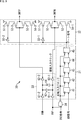
- FIG. FIG. 6 is a diagram illustrating a circuit configuration example of a clock enabler circuit in FIG. 5.
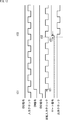
- 7 is a timing chart showing an operation of the clock enabler circuit of FIG. 6. It is a timing chart when not providing an input clock delay part. It is a figure which shows the circuit structural example of the clock enabler circuit corresponding to a differential input.
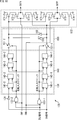
- FIG. 11 is a diagram illustrating a circuit configuration example of a clock enabler circuit of FIG. 10.
- 12 is a timing chart illustrating an operation of the clock enabler circuit of FIG. 11. It is a timing chart in case EN3 signal is always H.
- FIG. 11 is a diagram illustrating another circuit configuration example of the clock enabler circuit of FIG. 10.
- FIG. 11 is a diagram showing still another circuit configuration example of the clock enabler circuit of FIG. 10. It is a figure which shows the circuit structural example of the clock enabler circuit corresponding to a differential input.
- FIG. 1 is a block diagram showing a configuration example of a conventional clock enabler circuit.
- the clock enabler circuit 10 in FIG. 1 includes a gate signal generation unit 11 and a clock signal output unit 12.
- the gate signal generation unit 11 includes a flip-flop inside, generates a gate signal that enables the input clock based on an input clock from a clock generation circuit (not shown) and an enable signal (EN signal), This is supplied to the signal output unit 12.
- the clock signal output unit 12 outputs the output clock by enabling the input clock according to the level of the gate signal.
- the gate signal generation unit 11 uses the EN signal that has changed from the L (Low) level to the H (High) level as a gate signal. Output. There is a delay due to the flip-flop between the falling edge of the input clock and the output of the H level EN signal as the gate signal.
- the clock signal output unit 12 In this state, that is, when the input signal rises at time t2 in a state where the gate signal is at the H level, the clock signal output unit 12 outputs the output clock by enabling the input clock.
- the gate signal may be at the H level at time t3 while the input clock is at the H level.
- whisker also called a hazard
- the clock signal output unit of the clock enabler circuit to which the present technology is applied enables the timing of the level change from the L level to the H level of the EN signal from the time t11 to make the input clock effective.
- the gate signal is generated by delaying the timing when it does not occur, for example, between time t12 and time t13 when the input clock becomes L level.
- FIG. 5 is a block diagram illustrating a configuration example of the clock enabler circuit according to the first embodiment of the present technology.
- the clock enabler circuit 30 in FIG. 5 includes a gate signal generation unit 31, a clock signal output unit 32, and an input clock delay unit 33.
- the gate signal generation unit 31 generates a gate signal for enabling the input clock based on an input clock from a clock generation circuit (not shown) and the EN signal, and supplies the gate signal to the clock signal output unit 32.
- the gate signal generation unit 31 includes a delay circuit that delays the EN signal and a latch circuit that outputs the gate signal by latching the EN signal delayed by the delay circuit.
- the clock signal output unit 32 outputs the output clock by enabling the input clock from the input clock delay unit 33 according to the level of the gate signal from the gate signal generation unit 31.
- the input clock delay unit 33 delays an input clock from a clock generation circuit (not shown) and supplies it to the clock signal output unit 32.
- FIG. 6 is a diagram showing a circuit configuration example of the clock enabler circuit 30 of FIG.
- a NAND gate 34 is connected to the input terminal of the input clock of the gate signal generation unit 31, and the input clock and the second enable signal (EN2 signal) are input to the NAND gate 34.
- the NAND gate 34 supplies an inverted input clock obtained by inverting the input clock to the gate signal generation unit 31 when the EN2 signal becomes H level.
- the gate signal generation unit 31 in FIG. 6 includes four-stage flip-flops 41 to 44 and a latch circuit 45.
- the flip-flops 41 to 44 constitute a shift register by being connected in series. More specifically, the flip-flops 41 to 44 constitute a delay circuit that delays the EN signal by four pulses of the inverting input clock input thereto.
- the latch circuit 45 outputs a gate signal by latching the EN signal delayed by the flip-flops 41 to 44 (delay circuit).
- the gate signal generation unit 31 of FIG. 6 four stages of flip-flops are provided, but the number of stages is not limited to four. Further, instead of the latch circuit 45, a flip-flop may be provided.
- the 6 includes p-type transistors 51 and 52, n-type transistors 53 and 54, and an inverter 55.
- the p-type transistors 51 and 52 and the n-type transistors 53 and 54 constitute a switched inverter.
- One of the source and the drain of the p-type transistor 51 is connected to the power supply potential, and the other of the source and the drain is connected to one of the source and the drain of the p-type transistor 52.
- the other of the source and the drain of the p-type transistor 52 is connected to the output terminal.
- One of the source and drain of the n-type transistor 54 is connected to GND, and the other of the source and drain is connected to one of the source and drain of the n-type transistor 53.
- the other of the source and the drain of the n-type transistor 53 is connected to the output terminal.
- the gate of the p-type transistor 51 is connected to the output terminal of the gate signal generation unit 31 via the inverter 55, and the gate of the n-type transistor 54 is directly connected to the output terminal of the gate signal generation unit 31. .
- the gates of the p-type transistor 52 and the n-type transistor 53 are connected to the output terminal of the input clock delay unit 33.
- the clock signal output unit 32 outputs nothing regardless of the input clock from the input clock delay unit 33 when the gate signal is at the L level (the output clock remains at the H level). .
- the clock signal output unit 32 outputs a signal obtained by inverting the input clock from the input clock delay unit 33 as an output clock when the gate signal is at the H level.
- the input clock delay unit 33 in FIG. 6 includes two inverters 61 and 62 connected in series. With such a configuration, the input clock delay unit 33 outputs a delayed input clock obtained by delaying the input clock without changing the polarity of the input clock.
- the number of inverters constituting the input clock delay unit 33 is not limited to two and may be an even number.
- the NAND gate 34 When the input clock rises at time t31 while the EN2 signal is at the H level, the NAND gate 34 outputs the inverted input clock delayed by time d11 from time t31.
- the input clock delay unit 33 When the input clock rises at time t31, the input clock delay unit 33 outputs a delayed input clock delayed by time d12 from time t31.
- the flip-flops 41 to 44 delay the EN signal by 4 pulses of the inverted input clock.
- the latch circuit 45 latches the EN signal that has become H level at time t33 delayed by time d13 from time t32, and outputs it as a gate signal.
- the clock signal output unit 32 Since the gate signal is in the L level state until time t33, the clock signal output unit 32 outputs nothing regardless of the delayed input clock from the input clock delay unit 33 (the output clock is L level). . At time t33, the gate signal becomes H level, but since the delayed input clock from the input clock delay unit 33 is at H level, the output clock remains at L level.
- the clock signal output unit 32 starts to output a signal obtained by inverting the delayed input clock as an output clock.
- the gate signal is not activated at the timing when the delayed input clock is not valid. Changes to the H level, it is possible to reliably prevent the occurrence of whiskers in the output clock.
- the input clock is input to the clock enabler circuit 30 as a single end signal, but may be input as a differential signal.
- FIG. 9 is a diagram illustrating a circuit configuration example of the clock enabler circuit 30 in which the input clock is input as a differential signal.
- the differential input clocks INP and INN are input to the clock signal output unit 32 via the input clock delay unit 33.
- inverters 61-1 and 62-1 corresponding to the signal INP and inverters 61-2 and 62-2 corresponding to the signal INN.
- Cross-coupled inverters 63 and 64 are connected to the output sides of the inverters 61-1 and 61-2. As a result, the timings of changes in the signals output from the inverters 61-1 and 61-2 are matched.
- the clock signal output unit 32 of FIG. 9 corresponds to the p-type transistors 51-1 and 52-1 corresponding to the signal INP, the n-type transistors 53-1 and 54-1 and the inverter 55-1 and the signal INN.
- P-type transistors 51-2 and 52-2, n-type transistors 53-2 and 54-2, and an inverter 55-2 are provided.
- the p-type transistors 51-1 and 52-1 and the n-type transistors 53-1 and 54-1 are switched to the p-type transistors 51-2 and 52-2 and the n-type transistors 53-2 and 54-2, respectively. Configure the inverter.
- the input clock delay unit 33 is provided in order to adjust the timing when the gate signal becomes H level and the timing when the input clock is enabled.
- the inverter 55 (55-1, 55-2) is provided by configuring a switched inverter in the clock signal output unit 32, but this reduces the timing margin.
- FIG. 10 is a block diagram illustrating a configuration example of the clock enabler circuit according to the second embodiment of the present technology.
- 10 includes a gate signal generation unit 131 and a clock signal output unit 132.
- the gate signal generation unit 131 generates a gate signal for enabling the input clock based on an input clock from a clock generation circuit (not shown) and the EN signal, and supplies the gate signal to the clock signal output unit 132.
- the gate signal generation unit 131 includes a delay circuit that differentiates and delays the EN signal, and a latch circuit that outputs the gate signal by latching the EN signal that has been differentiated and delayed by the delay circuit.
- the clock signal output unit 132 outputs the output clock by enabling the input clock according to the level of the gate signal from the gate signal generation unit 131.
- FIG. 11 is a diagram illustrating a circuit configuration example of the clock enabler circuit 130.
- NAND gates 133-1 and 133-2 are connected to the input terminals of the input clock of the gate signal generation unit 131, and the input clocks are respectively connected to the NAND gates 133-1 and 133-2.
- a second enable signal EN2 signal. That is, the NAND gates 133-1 and 133-2 supply an inverted input clock obtained by inverting the input clock to the gate signal generation unit 131 when the EN2 signal becomes H level.
- the EN signal is directly input to the gate signal generation unit 131, and an inverted signal obtained by inverting the EN signal is input via the inverter 134.
- the gate signal generation unit 131 in FIG. 11 includes a delay circuit 140 and a latch circuit 150.
- the gate signal generation unit 131 in FIG. 11 includes a delay circuit 140 and a latch circuit 150.
- the delay circuit 140 includes a first shift register including four-stage flip-flops 141-1 to 144-1 and a second shift register including four-stage flip-flops 141-2 to 144-2. .
- the flip-flops 141-1 to 144-1 constitute a delay circuit that delays the EN signal by four pulses of the inverted input clock input to the NAND gate 133-1.
- the flip-flops 141-2 to 144-2 constitute a delay circuit that delays the inverted signal of the EN signal by four pulses of the inverted input clock input from the NAND gate 133-2.
- the inverted output of the second-stage flip-flop 142-1 in the first shift register is the input to the third-stage flip-flop 143-2 in the second shift register.
- the flip-flops 141-2 and 142-2 do not need to be electrically provided, but are provided in order to maintain symmetry between the first shift register and the second shift register.
- the inverted output of the second-stage flip-flop 142-1 of the first shift register is input to the third-stage flip-flop 143-2 of the second shift register.
- the inverted output of the nth flip-flop other than the second stage in the first shift register may be input to the (n + 1) th flip-flop of the second shift register.
- the timing at which the gate signal changes to the H level can be adjusted.
- the clock enabler circuit 130 may malfunction due to mismatch of the differentiated EN signals. Therefore, the inverted output of the nth flip-flop in the first shift register is input to the (n + 1) th flip-flop of the second shift register, so that the differential EN signal The influence of mismatch can be reduced.
- the latch circuit 150 includes transfer gates 151-1 and 151-2, a NOR gate 152, and a NAND gate 153.
- the transfer gate 151-1 becomes conductive in response to the inverted input clock from the NAND gate 133-1, so that the EN signal delayed by the first shift register (flip-flops 141-1 to 144-1) The signal is output to the clock signal output unit 132 as a gate signal.
- the transfer gate 151-2 becomes conductive in response to the inverted input clock from the NAND gate 133-2, so that the EN signal delayed by the second shift registers (flip-flops 141-2 to 144-2) is transferred. Outputs an inverted signal.
- the NOR gate 152 and the NAND gate 153 are configured as a latch unit that latches signals output from the transfer gates 151-1 and 151-2.
- the NOR gate 152 receives the output of the transfer gate 151-1 and the third enable signal (EN3 signal) for enabling the entire clock enabler circuit 130, and outputs them to the output side of the transfer gate 151-2.
- the NAND gate 153 receives the output of the transfer gate 151-2 and the EN3B signal, which is an inverted signal of the EN3 signal, and outputs them to the output side of the transfer gate 151-1.
- the NOR gate 152 determines the output of the transfer gate 151-2 at the H level.
- the output of the transfer gate 151-1 is fixed at the L level by the NAND gate 153.
- the NOR gate 152 determines the output of the transfer gate 151-2 at the L level. At this time, since the EN3B signal is in the H level, the output (gate signal) of the transfer gate 151-1 is fixed to the H level by the NAND gate 153.
- the output of the transfer gate 151-2 is fixed at the L level by the NOR gate 152 regardless of the output (gate signal) of the transfer gate 151-1.
- the output (gate signal) of the transfer gate 151-1 is fixed to the H level by the NAND gate 153.
- the logic is not determined only by the transfer gates 151-1 and 151-2, the logic is determined by the NOR gate 152 and the NAND gate 153 constituting the latch unit.
- the clock signal output unit 132 in FIG. 11 includes a NAND gate 161.
- the input clock and the output (gate signal) of the transfer gate 151-1 are input to output an output clock.
- the NAND gate 161 sets the output clock to H level regardless of the level of the input clock.
- the NAND gate 161 outputs a signal obtained by inverting the input clock as the output clock according to the change in the level of the input clock.
- the NAND gates 133-1 and 133-2 output the inverted input clock delayed by time d21 from time t51.
- the flip-flops 141-1 to 144-1 delay the EN signal by 4 inverted input clock pulses.
- the transfer gate 151-1 becomes conductive, and outputs an EN signal that has become H level with a delay of time d22 from time t52.
- the latch circuit 150 latches the EN signal and outputs it as a gate signal.
- the clock signal output unit 132 sets the output clock to the H level regardless of the input clock. Also, when the gate signal becomes H level after the time d22 has elapsed from time t52, the output clock remains H level because the input clock is L level.
- the clock signal output unit 132 starts outputting a signal obtained by inverting the input clock as the output clock.
- the gate signal is generated at a timing at which the input clock is not valid. Since it changes to the H level, it is possible to reliably prevent the occurrence of whiskers in the output clock.
- the clock enabler circuit 130 it seems as if the current consumption increases by making the EN signal differential. However, after the output of the output clock is started, the EN2 signal is set to the L level, so that the operation of the gate signal generation unit 131 (particularly the delay circuit 140) can be stopped while the gate signal level is maintained. Therefore, the current consumption does not increase as a whole.
- the EN3 signal is always at the L level.
- the EN3 signal does not depend on the EN signal or the EN2 signal. Since the output of the transfer gate 151-1 is fixed at the H level, a signal obtained by inverting the input clock is always output as the output clock.
- FIG. 14 is a diagram illustrating another circuit configuration example of the clock enabler circuit 130.
- the clock enabler circuit 130 of FIG. 14 is different from the NAND gate 161 in the clock signal output unit 132 in that p-type transistors 171, 172 and n-type transistors 173, 174 are provided. Different from 130.
- the p-type transistors 171 and 172 and the n-type transistors 173 and 174 constitute a switched inverter.
- the clock signal output unit 132 outputs nothing regardless of the input clock when the gate signal is at the L level, and a signal obtained by inverting the input clock when the gate signal is at the H level. Is output as an output clock.
- FIG. 15 is a diagram showing still another circuit configuration example of the clock enabler circuit 130.
- inverters 181 and 182 are provided in the latch circuit 150 in place of the NOR gate 152 and the NAND gate 153.
- the clock enabler circuit 130 of FIG. Inverters 181 and 182 are also configured as latch units that latch the signals output from transfer gates 151-1 and 151-2, respectively.
- the logic is not determined only by the transfer gates 151-1 and 151-2, the logic is determined by the inverters 181 and 182 constituting the latch unit.
- the input clock is input to the clock enabler circuit 130 as a single-ended signal, but may be input as a differential signal.
- FIG. 16 is a diagram illustrating a circuit configuration example of a clock enabler circuit in which an input clock is input as a differential signal.
- differential input clocks INP and INN are input to the clock signal output unit 132.
- 16 includes p-type transistors 171-1 and 172-1 and n-type transistors 173-1 and 174-1 corresponding to the signal INP, and a p-type transistor 171-2 corresponding to the signal INN. , 172-2, and n-type transistors 173-2 and 174-2.
- p-type transistors 171-1 and 172-1, n-type transistors 173-1 and 174-1, p-type transistors 171-2 and 172-2 corresponding to the signal INN, n-type transistors 173-2 and 174-2 Respectively constitute a switched inverter.
- the latch circuit 150 may be provided with a NOR gate 152 and a NAND gate 153 instead of the inverters 181 and 182.
- the clock signal output unit 132 includes p-type transistors 171-1 and 172-1, n-type transistors 173-1 and 174-1, p-type transistors 171-2 and 172-2, and n-type transistor 173-2. , 174-2, NAND gates corresponding to the signals INP and INN may be provided.
- the load of the clock signal output unit 132 serving as the output stage (the load of the clock path) is large, an inverter is connected before and after the transfer gates 151-1 and 151-2.
- the size of the transistor constituting the clock signal output unit 132 can be increased.
- Embodiments of the present technology are not limited to the above-described embodiments, and various modifications can be made without departing from the gist of the present technology.
- a gate signal generation unit that generates a gate signal that enables the input clock based on an input clock and an enable signal;
- a clock signal output unit that outputs an output clock by enabling the input clock according to the level of the gate signal; and
- the gate signal generation unit generates the gate signal by delaying the level change timing of the enable signal to a timing at which the input clock is not valid in the clock signal output unit.
- the gate signal generator is A delay circuit that differentially delays the enable signal;
- the latch circuit is A first transfer gate and a second transfer gate for outputting the differentiated enable signal by being turned on in accordance with an inverted input clock obtained by inverting the input clock; Latching each of the enable signals output from the first and second transfer gates, and The clock enabler circuit according to (2), wherein the enable signal from the latched first transfer gate is output as the gate signal.
- the latch unit receives an output of the first transfer gate as an input and outputs it to an output side of the second transfer gate, and an input of the output of the second transfer gate as an input.
- the clock enabler circuit according to (3) including a NAND gate that outputs to the output side.
- the latch unit receives the output of the first transfer gate as an input and outputs the first inverter to the output side of the second transfer gate, and the output of the second transfer gate as an input.
- the clock enabler circuit according to (3) including a second inverter that outputs to the output side of the transfer gate.
- the delay circuit is composed of first and second shift registers each consisting of n stages of flip-flops, The inverted output of the nth flip-flop in the first shift register becomes the input of the (n + 1) th flip-flop in the second shift register. (3) to (5) Clock enabler circuit.
- the gate signal generator is A delay circuit for delaying the enable signal; A latch circuit that outputs the gate signal by latching the enable signal delayed by the delay circuit;
- the clock enabler circuit according to (1) further comprising an input clock delay unit that delays the input clock input to the clock signal output unit.
- the clock enabler circuit according to (7) wherein the input clock delay unit is configured by connecting an even number of inverters in series.
- the clock signal output unit An inverter that inverts and outputs the gate signal;
- the delay circuit includes a shift register including a plurality of stages of flip-flops.
Landscapes
- Physics & Mathematics (AREA)
- Nonlinear Science (AREA)
- Manipulation Of Pulses (AREA)
Abstract
本技術は、出力クロックにおけるヒゲの発生を防止することができるようにするクロックイネーブラ回路に関する。 ゲート信号生成部は、入力クロックとイネーブル信号とに基づいて、入力クロックを有効にするゲート信号を生成し、クロック信号出力部は、ゲート信号のレベルに応じて入力クロックを有効にすることで、出力クロックを出力する。ゲート信号生成部は、イネーブル信号のレベル変化のタイミングを、クロック信号出力部において入力クロックが有効にならないタイミングまで遅延させることで、ゲート信号を生成する。本技術は、クロックイネーブラ回路に適用することができる。
Description
本技術は、クロックイネーブラ回路に関し、特に、出力クロックにおけるヒゲの発生を防止することができるようにするクロックイネーブラ回路に関する。
従来、クロックが必要な回路において、動作タイミング(クロックの入力タイミング)や、ロジック信号とのタイミングを揃えるためのクロックイネーブラ回路が知られている。クロックイネーブラ回路は、その前段のクロック生成回路の動作が安定するまで、後段にクロックを出力しないように動作する。
例えば、特許文献1には、イネーブル信号がハイレベルになってから、クロック生成回路からの入力クロックの数サイクル後に、出力クロックを出力するクロックイネーブラ回路が開示されている。
しかしながら、特許文献1に開示されるようなクロックイネーブラ回路に対して高速な動作が要求された場合、回路内のフリップフロップによる遅延のため、出力クロックに、ヒゲ(ハザードともいう)と呼ばれるパルス状のノイズが発生するおそれがある。
本技術は、このような状況に鑑みてなされたものであり、出力クロックにおけるヒゲの発生を防止することができるようにするものである。
本技術のクロックイネーブラ回路は、入力クロックとイネーブル信号とに基づいて、前記入力クロックを有効にするゲート信号を生成するゲート信号生成部と、前記ゲート信号のレベルに応じて前記入力クロックを有効にすることで、出力クロックを出力するクロック信号出力部とを備え、前記ゲート信号生成部は、前記イネーブル信号のレベル変化のタイミングを、前記クロック信号出力部において前記入力クロックが有効にならないタイミングまで遅延させることで、前記ゲート信号を生成する。
本技術においては、イネーブル信号のレベル変化のタイミングが、クロック信号出力部において入力クロックが有効にならないタイミングまで遅延されることで、ゲート信号が生成される。
本技術によれば、出力クロックにおけるヒゲの発生を防止することが可能となる。
なお、ここに記載された効果は必ずしも限定されるものではなく、本開示中に記載されたいずれかの効果であってもよい。
以下、本開示を実施するための形態(以下、実施の形態とする)について説明する。なお、説明は以下の順序で行う。
1.従来技術の課題と本技術の概要
2.第1の実施の形態
3.第2の実施の形態
2.第1の実施の形態
3.第2の実施の形態
<1.従来技術の課題と本技術の概要>
図1は、従来のクロックイネーブラ回路の構成例を示すブロック図である。
図1は、従来のクロックイネーブラ回路の構成例を示すブロック図である。
図1のクロックイネーブラ回路10は、ゲート信号生成部11およびクロック信号出力部12から構成される。
ゲート信号生成部11は、内部にフリップフロップを備え、図示せぬクロック生成回路からの入力クロックと、イネーブル信号(EN信号)とに基づいて、入力クロックを有効にするゲート信号を生成し、クロック信号出力部12に供給する。
クロック信号出力部12は、ゲート信号のレベルに応じて入力クロックを有効にすることで、出力クロックを出力する。
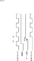
具体的には、図2に示されるように、ゲート信号生成部11は、時刻t1において入力クロックが立ち下がると、L(Low)レベルからH(High)レベルになったEN信号をゲート信号として出力する。入力クロックの立ち下がりからHレベルのEN信号がゲート信号として出力されるまでには、フリップフロップによる遅延が生じる。
この状態、すなわち、ゲート信号がHレベルの状態で、時刻t2において入力クロックが立ち上がると、クロック信号出力部12は、入力クロックを有効にすることで出力クロックを出力する。
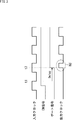
しかしながら、クロックイネーブラ回路10に対して高速な動作が要求された場合、図3に示されるように、入力クロックに対して、フリップフロップによる遅延が大きくなる。この場合、図3に示されるように、入力クロックがHレベルになっている間の時刻t3に、ゲート信号がHレベルになることがある。
このとき、クロック信号出力部12が、入力クロックを有効にすることで、出力クロックに、ヒゲ(ハザードともいう)と呼ばれるパルス状のノイズHdが発生してしまう。特に、入力クロックとEN信号とが非同期の場合、そのフリップフロップが1段であっても、ヒゲが発生するおそれがある。
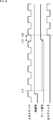
そこで、本技術を適用したクロックイネーブラ回路のクロック信号出力部は、図4に示されるように、EN信号のLレベルからHレベルへのレベル変化のタイミングを、時刻t11から、入力クロックが有効にならないタイミング、例えば、入力クロックがLレベルとなる時刻t12乃至t13の間まで遅延させることで、ゲート信号を生成するようにする。
<2.第1の実施の形態>
(クロックイネーブラ回路の構成例)
図5は、本技術の第1の実施の形態のクロックイネーブラ回路の構成例を示すブロック図である。
(クロックイネーブラ回路の構成例)
図5は、本技術の第1の実施の形態のクロックイネーブラ回路の構成例を示すブロック図である。
図5のクロックイネーブラ回路30は、ゲート信号生成部31、クロック信号出力部32、および入力クロック遅延部33から構成される。
ゲート信号生成部31は、図示せぬクロック生成回路からの入力クロックと、EN信号とに基づいて、入力クロックを有効にするゲート信号を生成し、クロック信号出力部32に供給する。ゲート信号生成部31は、EN信号を遅延させる遅延回路と、遅延回路により遅延されたEN信号をラッチすることでゲート信号を出力するラッチ回路を有する。
クロック信号出力部32は、ゲート信号生成部31からのゲート信号のレベルに応じて、入力クロック遅延部33からの入力クロックを有効にすることで、出力クロックを出力する。
入力クロック遅延部33は、図示せぬクロック生成回路からの入力クロックを遅延させて、クロック信号出力部32に供給する。
図6は、図5のクロックイネーブラ回路30の回路構成例を示す図である。
図6の例においては、ゲート信号生成部31の入力クロックの入力端に、NANDゲート34が接続されており、NANDゲート34には、入力クロックと第2のイネーブル信号(EN2信号)が入力される。すなわち、NANDゲート34は、EN2信号がHレベルになることで、入力クロックを反転した反転入力クロックを、ゲート信号生成部31に供給する。
図6のゲート信号生成部31は、4段のフリップフロップ41乃至44、およびラッチ回路45から構成される。
フリップフロップ41乃至44は、直列に接続されることでシフトレジスタを構成する。より具体的には、フリップフロップ41乃至44は、それぞれに入力される反転入力クロックの4パルス分、EN信号を遅延させる遅延回路を構成する。
ラッチ回路45は、フリップフロップ41乃至44(遅延回路)により遅延されたEN信号をラッチすることでゲート信号を出力する。
なお、図6のゲート信号生成部31においては、4段のフリップフロップが設けられるものとしたが、その段数は4段に限られない。また、ラッチ回路45に代えて、フリップフロップを設けるようにしてもよい。
図6のクロック信号出力部32は、p型トランジスタ51,52、n型トランジスタ53,54、およびインバータ55から構成される。p型トランジスタ51,52、n型トランジスタ53,54は、スイッチドインバータを構成する。
p型トランジスタ51のソースまたはドレインの一方は、電源電位に接続され、ソースまたはドレインの他方は、p型トランジスタ52のソースまたはドレインの一方に接続される。p型トランジスタ52のソースまたはドレインの他方は、出力端子に接続される。
n型トランジスタ54のソースまたはドレインの一方は、GNDに接続され、ソースまたはドレインの他方は、n型トランジスタ53のソースまたはドレインの一方に接続される。n型トランジスタ53のソースまたはドレインの他方は、出力端子に接続される。
また、p型トランジスタ51のゲートは、インバータ55を介して、ゲート信号生成部31の出力端に接続され、n型トランジスタ54のゲートは、直接、ゲート信号生成部31の出力端に接続される。そして、p型トランジスタ52およびn型トランジスタ53のゲートは、入力クロック遅延部33の出力端に接続される。
このような構成により、クロック信号出力部32は、ゲート信号がLレベルの状態では、入力クロック遅延部33からの入力クロックによらず、何も出力しない(出力クロックをHレベルのままとする)。また、クロック信号出力部32は、ゲート信号がHレベルの状態では、入力クロック遅延部33からの入力クロックを反転した信号を出力クロックとして出力する。
図6の入力クロック遅延部33は、直列に接続された2個のインバータ61,62から構成される。このような構成により、入力クロック遅延部33は、入力クロックの極性を変えることなく、入力クロックを遅延させた遅延入力クロックを出力する。なお、入力クロック遅延部33を構成するインバータの数は、2個に限らず、偶数個であればよい。
(クロックイネーブラ回路の動作)
次に、図7のタイミングチャートを参照して、図6のクロックイネーブラ回路30の動作について説明する。
次に、図7のタイミングチャートを参照して、図6のクロックイネーブラ回路30の動作について説明する。
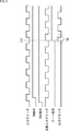
EN2信号がHレベルになった状態で、時刻t31において入力クロックが立ち上がると、NANDゲート34は、時刻t31から時間d11だけ遅延した反転入力クロックを出力する。
また、時刻t31において入力クロックが立ち上がると、入力クロック遅延部33は、時刻t31から時間d12だけ遅延した遅延入力クロックを出力する。
一方で、EN信号がHレベルになると、フリップフロップ41乃至44は、EN信号を、反転入力クロック4パルス分遅延させる。そして、時刻t32において、反転入力クロックが立ち下がると、ラッチ回路45は、時刻t32から時間d13だけ遅延させた時刻t33において、HレベルになったEN信号をラッチし、ゲート信号として出力する。
なお、時刻t33までは、ゲート信号がLレベルの状態であるので、クロック信号出力部32は、入力クロック遅延部33からの遅延入力クロックによらず、何も出力しない(出力クロックはLレベル)。また、時刻t33において、ゲート信号がHレベルになるが、入力クロック遅延部33からの遅延入力クロックがHレベルであるので、出力クロックはLレベルのままとなる。
そして、時刻t34において、遅延入力クロックが立ち下がると、クロック信号出力部32は、遅延入力クロックを反転した信号を、出力クロックとして出力し始める。
なお、入力クロック遅延部33を設けないで、入力クロックが直接、クロック信号出力部32に供給されるようにした場合、図8に示されるように、時刻t33において、ゲート信号がHレベルになると、入力クロックがLレベルであるので、出力クロックはHレベルとなり、ヒゲ(ノイズHd)が発生してしまう。
以上の動作によれば、クロックイネーブラ回路30に対して高速な動作が要求された場合や、入力クロックとイネーブル信号とが非同期の場合であっても、遅延入力クロックが有効にならないタイミングでゲート信号がHレベルに変化するので、確実に、出力クロックにおけるヒゲの発生を防止することが可能となる。
(他の回路構成例)
以上においては、入力クロックが、シングルエンド信号としてクロックイネーブラ回路30に入力されるようにしたが、差動信号として入力されるようにしてもよい。
以上においては、入力クロックが、シングルエンド信号としてクロックイネーブラ回路30に入力されるようにしたが、差動信号として入力されるようにしてもよい。
図9は、入力クロックが差動信号として入力されるようにしたクロックイネーブラ回路30の回路構成例を示す図である。
図9の例においては、差動入力クロックINP,INNが、入力クロック遅延部33を介して、クロック信号出力部32に入力される。
図9の入力クロック遅延部33には、信号INPに対応するインバータ61-1,62-1と、信号INNに対応するインバータ61-2,62-2とが設けられる。また、インバータ61-1,61-2の出力側には、クロスカップルインバータ63,64が接続される。これにより、インバータ61-1,61-2それぞれから出力される信号の変化のタイミングが一致するようになる。
図9のクロック信号出力部32には、信号INPに対応するp型トランジスタ51-1,52-1、n型トランジスタ53-1,54-1、およびインバータ55-1と、信号INNに対応するp型トランジスタ51-2,52-2、n型トランジスタ53-2,54-2、およびインバータ55-2とが設けられる。p型トランジスタ51-1,52-1、n型トランジスタ53-1,54-1と、p型トランジスタ51-2,52-2、n型トランジスタ53-2,54-2とは、それぞれスイッチドインバータを構成する。
このような構成により、入力クロックが差動信号として入力される場合であっても、確実に、出力クロックにおけるヒゲの発生を防止することが可能となる。
ところで、本実施の形態のクロックイネーブラ回路30においては、ゲート信号がHレベルになるタイミングと、入力クロックを有効にするタイミングとを調整するために、入力クロック遅延部33を設けるようにした。
しかしながら、入力クロックの伝送路であるクロックパスに入力クロック遅延部33(インバータ)を設けることで、ジッタが生じたり、消費電力が大きくなってしまう。
また、クロック信号出力部32内にスイッチドインバータを構成することで、インバータ55(55-1,55-2)を設けるようにしたが、これにより、タイミングマージンが小さくなってしまう。
そこで、以下においては、ジッタの発生や消費電力を抑えつつ、タイミングマージンを確保するようにした構成について説明する。
<3.第2の実施の形態>
(クロックイネーブラ回路の構成例)
図10は、本技術の第2の実施の形態のクロックイネーブラ回路の構成例を示すブロック図である。
(クロックイネーブラ回路の構成例)
図10は、本技術の第2の実施の形態のクロックイネーブラ回路の構成例を示すブロック図である。
図10のクロックイネーブラ回路130は、ゲート信号生成部131、およびクロック信号出力部132から構成される。
ゲート信号生成部131は、図示せぬクロック生成回路からの入力クロックと、EN信号とに基づいて、入力クロックを有効にするゲート信号を生成し、クロック信号出力部132に供給する。ゲート信号生成部131は、EN信号を差動化して遅延させる遅延回路と、遅延回路により差動化され遅延されたEN信号をラッチすることでゲート信号を出力するラッチ回路を有する。
クロック信号出力部132は、ゲート信号生成部131からのゲート信号のレベルに応じて、入力クロックを有効にすることで、出力クロックを出力する。
図11は、クロックイネーブラ回路130の回路構成例を示す図である。
図11の例においては、ゲート信号生成部131の入力クロックの入力端に、NANDゲート133-1,133-2が接続されており、NANDゲート133-1,133-2それぞれには、入力クロックと第2のイネーブル信号(EN2信号)が入力される。すなわち、NANDゲート133-1,133-2は、EN2信号がHレベルになることで、入力クロックを反転した反転入力クロックを、ゲート信号生成部131に供給する。
また、図11の例において、ゲート信号生成部131には、EN信号が直接入力される他、EN信号を反転した反転信号がインバータ134を介して入力される。
図11のゲート信号生成部131は、遅延回路140およびラッチ回路150を有する。
遅延回路140は、4段のフリップフロップ141-1乃至144-1からなる第1のシフトレジスタと、4段のフリップフロップ141-2乃至144-2からなる第2のシフトレジスタとから構成される。
フリップフロップ141-1乃至144-1は、NANDゲート133-1からそれぞれに入力される反転入力クロックの4パルス分、EN信号を遅延させる遅延回路を構成する。
フリップフロップ141-2乃至144-2は、NANDゲート133-2からそれぞれに入力される反転入力クロックの4パルス分、EN信号の反転信号を遅延させる遅延回路を構成する。
ただし、図11の例においては、第1のシフトレジスタにおける2段目のフリップフロップ142-1の反転出力が、第2のシフトレジスタにおける3段目のフリップフロップ143-2の入力となっている。したがって、フリップフロップ141-2,142-2は、電気的には設ける必要がないが、第1のシフトレジスタと第2のシフトレジスタとの対称性を保つために設けられている。
なお、図11の例では、第1のシフトレジスタの2段目のフリップフロップ142-1の反転出力が第2のシフトレジスタの3段目のフリップフロップ143-2に入力されるものとしたが、第1のシフトレジスタにおける2段目以外のn段目のフリップフロップの反転出力が第2のシフトレジスタの(n+1)段目のフリップフロップに入力されるようにしてもよい。
このように、EN信号を差動化することで、ゲート信号がHレベルに変化するタイミングを調整するようことができるようになる。しかしながら、単に、EN信号を差動化しただけでは、差動化されたEN信号のミスマッチにより、クロックイネーブラ回路130が誤動作するおそれがある。そこで、第1のシフトレジスタにおけるn段目のフリップフロップの反転出力が第2のシフトレジスタの(n+1)段目のフリップフロップに入力されるようにすることで、差動化されたEN信号のミスマッチの影響を低減することができる。
ラッチ回路150は、トランスファゲート151-1,151-2、NORゲート152、およびNANDゲート153から構成される。
トランスファゲート151-1は、NANDゲート133-1からの反転入力クロックに応じて導通状態となることで、第1のシフトレジスタ(フリップフロップ141-1乃至144-1)により遅延されたEN信号を、ゲート信号としてクロック信号出力部132に出力する。
トランスファゲート151-2は、NANDゲート133-2からの反転入力クロックに応じて導通状態となることで、第2のシフトレジスタ(フリップフロップ141-2乃至144-2)により遅延されたEN信号の反転信号を出力する。
NORゲート152およびNANDゲート153は、トランスファゲート151-1,151-2それぞれから出力された信号をラッチするラッチ部として構成される。
NORゲート152は、トランスファゲート151-1の出力と、クロックイネーブラ回路130全体を有効化する第3のイネーブル信号(EN3信号)とを入力として、トランスファゲート151-2の出力側に出力する。
NANDゲート153は、トランスファゲート151-2の出力と、EN3信号の反転信号であるEN3B信号とを入力として、トランスファゲート151-1の出力側に出力する。
例えば、EN3信号がLレベルの状態で、トランスファゲート151-1の出力(すなわちゲート信号)がLレベルの場合、NORゲート152により、トランスファゲート151-2の出力はHレベルに確定される。このとき、EN3B信号はHレベルの状態であるので、NANDゲート153により、トランスファゲート151-1の出力はLレベルに確定される。
また、EN3信号がLレベルの状態で、トランスファゲート151-1の出力(ゲート信号)がHレベルとなることで、NORゲート152により、トランスファゲート151-2の出力がLレベルに確定される。このとき、EN3B信号はHレベルの状態であるので、NANDゲート153により、トランスファゲート151-1の出力(ゲート信号)がHレベルに確定される。
なお、EN3信号がHレベルの場合、トランスファゲート151-1の出力(ゲート信号)によらず、NORゲート152により、トランスファゲート151-2の出力がLレベルに確定される。このとき、EN3B信号はLレベルの状態であるので、NANDゲート153により、トランスファゲート151-1の出力(ゲート信号)がHレベルに確定される。
このように、トランスファゲート151-1,151-2のみでは論理が確定されないため、ラッチ部を構成するNORゲート152およびNANDゲート153により、論理が確定されるようになる。
図11のクロック信号出力部132は、NANDゲート161から構成される。入力クロックと、トランスファゲート151-1の出力(ゲート信号)とを入力として、出力クロックを出力する。
トランスファゲート151-1の出力(ゲート信号)がLレベルの場合、入力クロックのレベルによらず、NANDゲート161により、出力クロックはHレベルとなる。トランスファゲート151-1の出力(ゲート信号)がHレベルの場合、入力クロックのレベルの変化に応じて、NANDゲート161により、入力クロックを反転した信号が出力クロックとして出力される。
(クロックイネーブラ回路の動作)
次に、図12のタイミングチャートを参照して、図11のクロックイネーブラ回路130の動作について説明する。
次に、図12のタイミングチャートを参照して、図11のクロックイネーブラ回路130の動作について説明する。
図12の例では、EN3信号は常時Lレベルをとるものとする。
EN2信号がHレベルになった状態で、時刻t51において入力クロックが立ち上がると、NANDゲート133-1,133-2は、時刻t51から時間d21だけ遅延した反転入力クロックを出力する。
一方で、EN信号がHレベルになると、フリップフロップ141-1乃至144-1は、EN信号を、反転入力クロック4パルス分遅延させる。そして、時刻t52において、反転入力クロックが立ち上がると、トランスファゲート151-1は、導通状態となり、時刻t52から時間d22だけ遅延させて、HレベルになったEN信号を出力する。ラッチ回路150は、そのEN信号をラッチし、ゲート信号として出力する。
なお、ここまでは、ゲート信号がLレベルの状態であるので、クロック信号出力部132は、入力クロックにかかわらず、出力クロックをHレベルとする。また、時刻t52から時間d22経過後、ゲート信号がHレベルになったときも、入力クロックがLレベルであるので、出力クロックはHレベルのままとなる。
そして、時刻t53において、入力クロックが立ち上がると、クロック信号出力部132は、入力クロックを反転した信号を、出力クロックとして出力し始める。
以上の動作によれば、クロックイネーブラ回路130に対して高速な動作が要求された場合や、入力クロックとイネーブル信号とが非同期の場合であっても、入力クロックが有効にならないタイミングでゲート信号がHレベルに変化するので、確実に、出力クロックにおけるヒゲの発生を防止することが可能となる。
また、入力クロックの伝送路であるクロックパスに入力クロック遅延部(インバータ)を設ける必要がなく、クロック信号出力部132内にインバータを設ける必要もないので、ジッタの発生や消費電力を抑えつつ、タイミングマージンを確保することが可能となる。
なお、クロックイネーブラ回路130においては、EN信号を差動化したことで、消費電流が増大するかのようにみえる。しかしながら、出力クロックの出力開始後は、EN2信号をLレベルにすることで、ゲート信号のレベルを保持したまま、ゲート信号生成部131(特に遅延回路140)の動作を停止することができる。そのため、全体として消費電流が増大することはない。
また、図12の例では、EN3信号は常時Lレベルをとるものとしたが、図13に示されるように、EN3信号が常時Hレベルをとるようにした場合、EN信号やEN2信号によらず、トランスファゲート151-1の出力がHレベルに確定されることで、常時、入力クロックを反転した信号が出力クロックとして出力されるようになる。
(他の回路構成例)
図14は、クロックイネーブラ回路130の他の回路構成例を示す図である。
図14は、クロックイネーブラ回路130の他の回路構成例を示す図である。
図14のクロックイネーブラ回路130は、クロック信号出力部132に、NANDゲート161に代えて、p型トランジスタ171,172、n型トランジスタ173,174が設けられている点で、図11のクロックイネーブラ回路130と異なる。p型トランジスタ171,172、n型トランジスタ173,174は、スイッチドインバータを構成する。
このような構成においても、クロック信号出力部132は、ゲート信号がLレベルの状態では、入力クロックにかかわらず、何も出力せず、ゲート信号がHレベルの状態では、入力クロックを反転した信号を出力クロックとして出力する。
図15は、クロックイネーブラ回路130のさらに他の回路構成例を示す図である。
図15のクロックイネーブラ回路130は、ラッチ回路150に、NORゲート152およびNANDゲート153に代えて、インバータ181,182が設けられている点で、図14のクロックイネーブラ回路130と異なる。インバータ181,182もまた、トランスファゲート151-1,151-2それぞれから出力された信号をラッチするラッチ部として構成される。
このような構成においても、トランスファゲート151-1,151-2のみでは論理が確定されないため、ラッチ部を構成するインバータ181,182により、論理が確定されるようになる。
なお、以上においては、入力クロックが、シングルエンド信号としてクロックイネーブラ回路130に入力されるようにしたが、差動信号として入力されるようにしてもよい。
図16は、入力クロックが差動信号として入力されるようにしたクロックイネーブラ回路の回路構成例を示す図である。
図16の例においては、差動入力クロックINP,INNが、クロック信号出力部132に入力される。
図16のクロック信号出力部132には、信号INPに対応するp型トランジスタ171-1,172-1、n型トランジスタ173-1,174-1と、信号INNに対応するp型トランジスタ171-2,172-2、n型トランジスタ173-2,174-2とが設けられる。p型トランジスタ171-1,172-1、n型トランジスタ173-1,174-1と、信号INNに対応するp型トランジスタ171-2,172-2、n型トランジスタ173-2,174-2とは、それぞれスイッチドインバータを構成する。
このような構成により、同じく入力クロックが差動信号として入力される図9の構成と比較しても、入力クロックの伝送路であるクロックパスにクロスカップルインバータを含む入力クロック遅延部を設ける必要がなく、クロック信号出力部132内にインバータを設ける必要もないので、ジッタや消費電力を抑えつつ、タイミングマージンを確保することが可能となる。
また、図16の例においては、ラッチ回路150に、インバータ181,182に代えて、NORゲート152およびNANDゲート153が設けられるようにしてもよい。さらに、クロック信号出力部132に、p型トランジスタ171-1,172-1、n型トランジスタ173-1,174-1、および、p型トランジスタ171-2,172-2、n型トランジスタ173-2,174-2に代えて、信号INP,INNそれぞれに対応するNANDゲートが設けられるようにしてもよい。
なお、本実施の形態において、出力段となるクロック信号出力部132の負荷(クロックパスの負荷)が大きい場合には、トランスファゲート151-1,151-2の前段および後段にインバータを接続することで、クロック信号出力部132を構成するトランジスタのサイズを大きくすることができる。
本技術の実施の形態は、上述した実施の形態に限定されるものではなく、本技術の要旨を逸脱しない範囲において種々の変更が可能である。
さらに、本技術は以下のような構成をとることができる。
(1)
入力クロックとイネーブル信号とに基づいて、前記入力クロックを有効にするゲート信号を生成するゲート信号生成部と、
前記ゲート信号のレベルに応じて前記入力クロックを有効にすることで、出力クロックを出力するクロック信号出力部と
を備え、
前記ゲート信号生成部は、前記イネーブル信号のレベル変化のタイミングを、前記クロック信号出力部において前記入力クロックが有効にならないタイミングまで遅延させることで、前記ゲート信号を生成する
クロックイネーブラ回路。
(2)
前記ゲート信号生成部は、
前記イネーブル信号を差動化して遅延させる遅延回路と、
前記遅延回路により差動化され遅延された前記イネーブル信号をラッチすることで前記ゲート信号を出力するラッチ回路と
を有する
(1)に記載のクロックイネーブラ回路。
(3)
前記ラッチ回路は、
前記入力クロックを反転した反転入力クロックに応じて導通状態となることで、差動化された前記イネーブル信号を出力する第1および第2のトランスファゲートと、
前記第1および第2のトランスファゲートから出力された前記イネーブル信号それぞれをラッチするラッチ部と
を有し、
ラッチされた前記第1のトランスファゲートからの前記イネーブル信号を、前記ゲート信号として出力する
(2)に記載のクロックイネーブラ回路。
(4)
前記ラッチ部は、前記第1のトランスファゲートの出力を入力として前記第2のトランスファゲートの出力側に出力するNORゲート、および、前記第2のトランスファゲートの出力を入力として前記第1のトランスファゲートの出力側に出力するNANDゲートから構成される
(3)に記載のクロックイネーブラ回路。
(5)
前記ラッチ部は、前記第1のトランスファゲートの出力を入力として前記第2のトランスファゲートの出力側に出力する第1のインバータ、および、前記第2のトランスファゲートの出力を入力として前記第1のトランスファゲートの出力側に出力する第2のインバータから構成される
(3)に記載のクロックイネーブラ回路。
(6)
前記遅延回路は、それぞれn段のフリップフロップからなる第1および第2のシフトレジスタから構成され、
前記第1のシフトレジスタにおけるn段目のフリップフロップの反転出力が、前記第2のシフトレジスタにおける(n+1)段目のフリップフロップの入力となる
(3)乃至(5)のいずれかに記載のクロックイネーブラ回路。
(7)
前記ゲート信号生成部は、
前記イネーブル信号を遅延させる遅延回路と、
前記遅延回路により遅延された前記イネーブル信号をラッチすることで前記ゲート信号を出力するラッチ回路と
を有し、
前記クロック信号出力部に入力される前記入力クロックを遅延させる入力クロック遅延部をさらに備える
(1)に記載のクロックイネーブラ回路。
(8)
前記入力クロック遅延部は、偶数個のインバータが直列に接続されることで構成される
(7)に記載のクロックイネーブラ回路。
(9)
前記クロック信号出力部は、
前記ゲート信号を反転して出力するインバータと、
前記ゲート信号と、前記インバータから出力される反転ゲート信号とに基づいて、前記出力クロックを出力するスイッチドインバータと
を有する
(7)または(8)に記載のクロックイネーブラ回路。
(10)
前記遅延回路は、複数段のフリップフロップからなるシフトレジスタから構成される
(7)乃至(9)のいずれかに記載のクロックイネーブラ回路。
(11)
前記入力クロックは、シングルエンド信号である
(1)乃至(10)のいずれかに記載のクロックイネーブラ回路。
(12)
前記入力クロックは、差動信号である
(1)乃至(10)のいずれかに記載のクロックイネーブラ回路。
(1)
入力クロックとイネーブル信号とに基づいて、前記入力クロックを有効にするゲート信号を生成するゲート信号生成部と、
前記ゲート信号のレベルに応じて前記入力クロックを有効にすることで、出力クロックを出力するクロック信号出力部と
を備え、
前記ゲート信号生成部は、前記イネーブル信号のレベル変化のタイミングを、前記クロック信号出力部において前記入力クロックが有効にならないタイミングまで遅延させることで、前記ゲート信号を生成する
クロックイネーブラ回路。
(2)
前記ゲート信号生成部は、
前記イネーブル信号を差動化して遅延させる遅延回路と、
前記遅延回路により差動化され遅延された前記イネーブル信号をラッチすることで前記ゲート信号を出力するラッチ回路と
を有する
(1)に記載のクロックイネーブラ回路。
(3)
前記ラッチ回路は、
前記入力クロックを反転した反転入力クロックに応じて導通状態となることで、差動化された前記イネーブル信号を出力する第1および第2のトランスファゲートと、
前記第1および第2のトランスファゲートから出力された前記イネーブル信号それぞれをラッチするラッチ部と
を有し、
ラッチされた前記第1のトランスファゲートからの前記イネーブル信号を、前記ゲート信号として出力する
(2)に記載のクロックイネーブラ回路。
(4)
前記ラッチ部は、前記第1のトランスファゲートの出力を入力として前記第2のトランスファゲートの出力側に出力するNORゲート、および、前記第2のトランスファゲートの出力を入力として前記第1のトランスファゲートの出力側に出力するNANDゲートから構成される
(3)に記載のクロックイネーブラ回路。
(5)
前記ラッチ部は、前記第1のトランスファゲートの出力を入力として前記第2のトランスファゲートの出力側に出力する第1のインバータ、および、前記第2のトランスファゲートの出力を入力として前記第1のトランスファゲートの出力側に出力する第2のインバータから構成される
(3)に記載のクロックイネーブラ回路。
(6)
前記遅延回路は、それぞれn段のフリップフロップからなる第1および第2のシフトレジスタから構成され、
前記第1のシフトレジスタにおけるn段目のフリップフロップの反転出力が、前記第2のシフトレジスタにおける(n+1)段目のフリップフロップの入力となる
(3)乃至(5)のいずれかに記載のクロックイネーブラ回路。
(7)
前記ゲート信号生成部は、
前記イネーブル信号を遅延させる遅延回路と、
前記遅延回路により遅延された前記イネーブル信号をラッチすることで前記ゲート信号を出力するラッチ回路と
を有し、
前記クロック信号出力部に入力される前記入力クロックを遅延させる入力クロック遅延部をさらに備える
(1)に記載のクロックイネーブラ回路。
(8)
前記入力クロック遅延部は、偶数個のインバータが直列に接続されることで構成される
(7)に記載のクロックイネーブラ回路。
(9)
前記クロック信号出力部は、
前記ゲート信号を反転して出力するインバータと、
前記ゲート信号と、前記インバータから出力される反転ゲート信号とに基づいて、前記出力クロックを出力するスイッチドインバータと
を有する
(7)または(8)に記載のクロックイネーブラ回路。
(10)
前記遅延回路は、複数段のフリップフロップからなるシフトレジスタから構成される
(7)乃至(9)のいずれかに記載のクロックイネーブラ回路。
(11)
前記入力クロックは、シングルエンド信号である
(1)乃至(10)のいずれかに記載のクロックイネーブラ回路。
(12)
前記入力クロックは、差動信号である
(1)乃至(10)のいずれかに記載のクロックイネーブラ回路。
30 クロックイネーブラ回路, 31 ゲート信号生成部, 32 クロック信号出力部, 33 入力クロック遅延部, 41乃至44 フリップフロップ, 45 ラッチ回路, 51,52 p型トランジスタ, 53,54 n型トランジスタ, 55 インバータ, 61,62 インバータ, 130 クロックイネーブラ回路, 131 ゲート信号生成部, 132 クロック信号出力部, 140 遅延回路, 141-1乃至144-1,141-2乃至144-2 フリップフロップ, 150 ラッチ回路, 151-1,151-2 トランスファゲート, 152 NORゲート, 153 NANDゲート, 161 NANDゲート, 171,172 p型トランジスタ, 173,174 n型トランジスタ, 181,182 インバータ
Claims (12)
- 入力クロックとイネーブル信号とに基づいて、前記入力クロックを有効にするゲート信号を生成するゲート信号生成部と、
前記ゲート信号のレベルに応じて前記入力クロックを有効にすることで、出力クロックを出力するクロック信号出力部と
を備え、
前記ゲート信号生成部は、前記イネーブル信号のレベル変化のタイミングを、前記クロック信号出力部において前記入力クロックが有効にならないタイミングまで遅延させることで、前記ゲート信号を生成する
クロックイネーブラ回路。 - 前記ゲート信号生成部は、
前記イネーブル信号を差動化して遅延させる遅延回路と、
前記遅延回路により差動化され遅延された前記イネーブル信号をラッチすることで前記ゲート信号を出力するラッチ回路と
を有する
請求項1に記載のクロックイネーブラ回路。 - 前記ラッチ回路は、
前記入力クロックを反転した反転入力クロックに応じて導通状態となることで、差動化された前記イネーブル信号を出力する第1および第2のトランスファゲートと、
前記第1および第2のトランスファゲートから出力された前記イネーブル信号それぞれをラッチするラッチ部と
を有し、
ラッチされた前記第1のトランスファゲートからの前記イネーブル信号を、前記ゲート信号として出力する
請求項2に記載のクロックイネーブラ回路。 - 前記ラッチ部は、前記第1のトランスファゲートの出力を入力として前記第2のトランスファゲートの出力側に出力するNORゲート、および、前記第2のトランスファゲートの出力を入力として前記第1のトランスファゲートの出力側に出力するNANDゲートから構成される
請求項3に記載のクロックイネーブラ回路。 - 前記ラッチ部は、前記第1のトランスファゲートの出力を入力として前記第2のトランスファゲートの出力側に出力する第1のインバータ、および、前記第2のトランスファゲートの出力を入力として前記第1のトランスファゲートの出力側に出力する第2のインバータから構成される
請求項3に記載のクロックイネーブラ回路。 - 前記遅延回路は、それぞれn段のフリップフロップからなる第1および第2のシフトレジスタから構成され、
前記第1のシフトレジスタにおけるn段目のフリップフロップの反転出力が、前記第2のシフトレジスタにおける(n+1)段目のフリップフロップの入力となる
請求項3に記載のクロックイネーブラ回路。 - 前記ゲート信号生成部は、
前記イネーブル信号を遅延させる遅延回路と、
前記遅延回路により遅延された前記イネーブル信号をラッチすることで前記ゲート信号を出力するラッチ回路と
を有し、
前記クロック信号出力部に入力される前記入力クロックを遅延させる入力クロック遅延部をさらに備える
請求項1に記載のクロックイネーブラ回路。 - 前記入力クロック遅延部は、偶数個のインバータが直列に接続されることで構成される
請求項7に記載のクロックイネーブラ回路。 - 前記クロック信号出力部は、
前記ゲート信号を反転して出力するインバータと、
前記ゲート信号と、前記インバータから出力される反転ゲート信号とに基づいて、前記出力クロックを出力するスイッチドインバータと
を有する
請求項7に記載のクロックイネーブラ回路。 - 前記遅延回路は、複数段のフリップフロップからなるシフトレジスタから構成される
請求項7に記載のクロックイネーブラ回路。 - 前記入力クロックは、シングルエンド信号である
請求項1に記載のクロックイネーブラ回路。 - 前記入力クロックは、差動信号である
請求項1に記載のクロックイネーブラ回路。
Priority Applications (1)
| Application Number | Priority Date | Filing Date | Title |
|---|---|---|---|
| JP2019525290A JP7218289B2 (ja) | 2017-06-13 | 2018-05-30 | クロックイネーブラ回路 |
Applications Claiming Priority (2)
| Application Number | Priority Date | Filing Date | Title |
|---|---|---|---|
| JP2017-115826 | 2017-06-13 | ||
| JP2017115826 | 2017-06-13 |
Publications (1)
| Publication Number | Publication Date |
|---|---|
| WO2018230338A1 true WO2018230338A1 (ja) | 2018-12-20 |
Family
ID=64660258
Family Applications (1)
| Application Number | Title | Priority Date | Filing Date |
|---|---|---|---|
| PCT/JP2018/020651 Ceased WO2018230338A1 (ja) | 2017-06-13 | 2018-05-30 | クロックイネーブラ回路 |
Country Status (2)
| Country | Link |
|---|---|
| JP (1) | JP7218289B2 (ja) |
| WO (1) | WO2018230338A1 (ja) |
Cited By (2)
| Publication number | Priority date | Publication date | Assignee | Title |
|---|---|---|---|---|
| WO2021152938A1 (ja) * | 2020-01-29 | 2021-08-05 | ソニーセミコンダクタソリューションズ株式会社 | クロックイネーブラ回路 |
| CN117134746A (zh) * | 2022-05-19 | 2023-11-28 | 上海韦尔半导体股份有限公司 | 时钟产生电路 |
Citations (3)
| Publication number | Priority date | Publication date | Assignee | Title |
|---|---|---|---|---|
| JPH11506885A (ja) * | 1995-06-07 | 1999-06-15 | サムソン・エレクトロニクス・カンパニー・リミテッド | グリッチの生じないクロックイネーブル回路 |
| JP2000068800A (ja) * | 1998-08-24 | 2000-03-03 | Nec Eng Ltd | ヒゲ防止方式及び回路 |
| JP2000357953A (ja) * | 1999-06-14 | 2000-12-26 | Namco Ltd | ゲーテッド・クロック信号生成回路および方法 |
-
2018
- 2018-05-30 WO PCT/JP2018/020651 patent/WO2018230338A1/ja not_active Ceased
- 2018-05-30 JP JP2019525290A patent/JP7218289B2/ja active Active
Patent Citations (3)
| Publication number | Priority date | Publication date | Assignee | Title |
|---|---|---|---|---|
| JPH11506885A (ja) * | 1995-06-07 | 1999-06-15 | サムソン・エレクトロニクス・カンパニー・リミテッド | グリッチの生じないクロックイネーブル回路 |
| JP2000068800A (ja) * | 1998-08-24 | 2000-03-03 | Nec Eng Ltd | ヒゲ防止方式及び回路 |
| JP2000357953A (ja) * | 1999-06-14 | 2000-12-26 | Namco Ltd | ゲーテッド・クロック信号生成回路および方法 |
Cited By (5)
| Publication number | Priority date | Publication date | Assignee | Title |
|---|---|---|---|---|
| WO2021152938A1 (ja) * | 2020-01-29 | 2021-08-05 | ソニーセミコンダクタソリューションズ株式会社 | クロックイネーブラ回路 |
| JPWO2021152938A1 (ja) * | 2020-01-29 | 2021-08-05 | ||
| US12126345B2 (en) | 2020-01-29 | 2024-10-22 | Sony Semiconductor Solutions Corporation | Clock enabler circuit |
| JP7691940B2 (ja) | 2020-01-29 | 2025-06-12 | ソニーセミコンダクタソリューションズ株式会社 | クロックイネーブラ回路 |
| CN117134746A (zh) * | 2022-05-19 | 2023-11-28 | 上海韦尔半导体股份有限公司 | 时钟产生电路 |
Also Published As
| Publication number | Publication date |
|---|---|
| JP7218289B2 (ja) | 2023-02-06 |
| JPWO2018230338A1 (ja) | 2020-04-16 |
Similar Documents
| Publication | Publication Date | Title |
|---|---|---|
| US7408393B1 (en) | Master-slave flip-flop and clocking scheme | |
| US9853630B2 (en) | Skew-tolerant flip-flop | |
| CN101977037B (zh) | 脉冲时钟产生电路、集成电路与产生脉冲时钟信号的方法 | |
| US8963646B1 (en) | Delay line ring oscillation apparatus | |
| US20080074151A1 (en) | Dual-edge-triggered, clock-gated logic circuit and method | |
| US20150130520A1 (en) | Timing adjustment circuit and semiconductor integrated circuit device | |
| US20150381154A1 (en) | Flip-flop circuit | |
| JP7218289B2 (ja) | クロックイネーブラ回路 | |
| KR100911190B1 (ko) | 내부 클럭 드라이버 회로 | |
| US9537477B2 (en) | Semiconductor apparatus capable of converting a frequency of an input clock | |
| US8854093B2 (en) | Multi-phase clock generation circuit | |
| Parthibhan et al. | Clock skew optimization in pre and post CTS | |
| US7492205B2 (en) | Clock generator | |
| CN107592099B (zh) | D触发器 | |
| JP2008109608A (ja) | フリップフロップ回路 | |
| US10141920B2 (en) | Clock signal controller | |
| US20050189977A1 (en) | Double-edge-trigger flip-flop | |
| KR100980413B1 (ko) | 클럭 버퍼 및 이를 이용하는 반도체 메모리 장치 | |
| TWI583137B (zh) | 同步器正反器 | |
| US9197197B2 (en) | Duty cycle protection circuit | |
| JP5212934B2 (ja) | 集積回路装置 | |
| JP5881655B2 (ja) | 半導体集積回路装置 | |
| US9660615B2 (en) | Flip-flop devices with clock sharing | |
| KR102961846B1 (ko) | D 플립플롭, d 플립플롭을 포함하는 프로세서 및 컴퓨팅 장치 | |
| KR102800001B1 (ko) | 데이터 듀티 스큐를 완화하는 데이터 직렬화기 |
Legal Events
| Date | Code | Title | Description |
|---|---|---|---|
| 121 | Ep: the epo has been informed by wipo that ep was designated in this application |
Ref document number: 18818783 Country of ref document: EP Kind code of ref document: A1 |
|
| ENP | Entry into the national phase |
Ref document number: 2019525290 Country of ref document: JP Kind code of ref document: A |
|
| NENP | Non-entry into the national phase |
Ref country code: DE |
|
| 122 | Ep: pct application non-entry in european phase |
Ref document number: 18818783 Country of ref document: EP Kind code of ref document: A1 |