WO2018209946A1 - 触控显示面板、显示装置及触控显示面板的驱动方法 - Google Patents
触控显示面板、显示装置及触控显示面板的驱动方法 Download PDFInfo
- Publication number
- WO2018209946A1 WO2018209946A1 PCT/CN2017/116517 CN2017116517W WO2018209946A1 WO 2018209946 A1 WO2018209946 A1 WO 2018209946A1 CN 2017116517 W CN2017116517 W CN 2017116517W WO 2018209946 A1 WO2018209946 A1 WO 2018209946A1
- Authority
- WO
- WIPO (PCT)
- Prior art keywords
- self
- display panel
- touch display
- capacitance
- pixels
- Prior art date
- Legal status (The legal status is an assumption and is not a legal conclusion. Google has not performed a legal analysis and makes no representation as to the accuracy of the status listed.)
- Ceased
Links
Images




Classifications
-
- G—PHYSICS
- G06—COMPUTING OR CALCULATING; COUNTING
- G06F—ELECTRIC DIGITAL DATA PROCESSING
- G06F3/00—Input arrangements for transferring data to be processed into a form capable of being handled by the computer; Output arrangements for transferring data from processing unit to output unit, e.g. interface arrangements
- G06F3/01—Input arrangements or combined input and output arrangements for interaction between user and computer
- G06F3/03—Arrangements for converting the position or the displacement of a member into a coded form
- G06F3/041—Digitisers, e.g. for touch screens or touch pads, characterised by the transducing means
- G06F3/0412—Digitisers structurally integrated in a display
-
- G—PHYSICS
- G06—COMPUTING OR CALCULATING; COUNTING
- G06F—ELECTRIC DIGITAL DATA PROCESSING
- G06F3/00—Input arrangements for transferring data to be processed into a form capable of being handled by the computer; Output arrangements for transferring data from processing unit to output unit, e.g. interface arrangements
- G06F3/01—Input arrangements or combined input and output arrangements for interaction between user and computer
- G06F3/03—Arrangements for converting the position or the displacement of a member into a coded form
- G06F3/041—Digitisers, e.g. for touch screens or touch pads, characterised by the transducing means
- G06F3/0416—Control or interface arrangements specially adapted for digitisers
- G06F3/04164—Connections between sensors and controllers, e.g. routing lines between electrodes and connection pads
-
- G—PHYSICS
- G06—COMPUTING OR CALCULATING; COUNTING
- G06F—ELECTRIC DIGITAL DATA PROCESSING
- G06F3/00—Input arrangements for transferring data to be processed into a form capable of being handled by the computer; Output arrangements for transferring data from processing unit to output unit, e.g. interface arrangements
- G06F3/01—Input arrangements or combined input and output arrangements for interaction between user and computer
- G06F3/03—Arrangements for converting the position or the displacement of a member into a coded form
- G06F3/041—Digitisers, e.g. for touch screens or touch pads, characterised by the transducing means
- G06F3/044—Digitisers, e.g. for touch screens or touch pads, characterised by the transducing means by capacitive means
-
- G—PHYSICS
- G06—COMPUTING OR CALCULATING; COUNTING
- G06F—ELECTRIC DIGITAL DATA PROCESSING
- G06F3/00—Input arrangements for transferring data to be processed into a form capable of being handled by the computer; Output arrangements for transferring data from processing unit to output unit, e.g. interface arrangements
- G06F3/01—Input arrangements or combined input and output arrangements for interaction between user and computer
- G06F3/03—Arrangements for converting the position or the displacement of a member into a coded form
- G06F3/041—Digitisers, e.g. for touch screens or touch pads, characterised by the transducing means
- G06F3/044—Digitisers, e.g. for touch screens or touch pads, characterised by the transducing means by capacitive means
- G06F3/0443—Digitisers, e.g. for touch screens or touch pads, characterised by the transducing means by capacitive means using a single layer of sensing electrodes
-
- G—PHYSICS
- G06—COMPUTING OR CALCULATING; COUNTING
- G06F—ELECTRIC DIGITAL DATA PROCESSING
- G06F3/00—Input arrangements for transferring data to be processed into a form capable of being handled by the computer; Output arrangements for transferring data from processing unit to output unit, e.g. interface arrangements
- G06F3/01—Input arrangements or combined input and output arrangements for interaction between user and computer
- G06F3/03—Arrangements for converting the position or the displacement of a member into a coded form
- G06F3/041—Digitisers, e.g. for touch screens or touch pads, characterised by the transducing means
- G06F3/0416—Control or interface arrangements specially adapted for digitisers
- G06F3/04166—Details of scanning methods, e.g. sampling time, grouping of sub areas or time sharing with display driving
Definitions
- the present disclosure relates to the field of display technologies, and in particular, to a touch display panel, a display device, and a driving method of the touch display panel.
- the Touch Screen Panel With the rapid development of display technology, the Touch Screen Panel has gradually spread throughout people's lives.
- the touch screen can be divided into an add-on touch panel, an on-cell touch panel, and an in-cell touch panel according to the composition structure.
- the external touch screen is produced by separately separating the touch screen from the liquid crystal display (LCD), and then being bonded together to become a liquid crystal display with touch function.
- the external touch screen has higher production cost and light transmittance. Low, thicker modules and other shortcomings.
- the in-cell touch screen embeds the touch electrode of the touch screen inside the liquid crystal display, which can reduce the overall thickness of the module, and can greatly reduce the manufacturing cost of the touch screen, and is favored by major panel manufacturers.
- Some embodiments of the present disclosure provide a touch display panel, a display device, and a driving method of the touch display panel.
- a touch display panel includes: an upper substrate, a lower substrate disposed opposite the upper substrate; and a matrix arranged between the upper substrate and the lower substrate a driving chip configured to perform progressive scanning on the plurality of pixels; a common electrode layer between the upper substrate and the lower substrate, which is divided into a plurality of independent self-capacitance electrodes, The self-capacitance electrode is connected to the driving chip through a corresponding wire,
- the driving chip is further configured to apply a common electrode signal to the corresponding row self-capacitance electrodes only when the pixels corresponding to the respective rows of self-capacitance electrodes are in a scanning state.
- each row of self-capacitance electrodes corresponds to a plurality of rows of pixels.
- the number of rows of pixels corresponding to each row of self-capacitance electrodes is the same.
- the method further includes: a plurality of compensation resistors electrically connected to the plurality of wires, and a resistance value of each compensation resistor and a corresponding wire The length is negatively correlated.
- the touch display panel provided by some embodiments of the present disclosure further includes: a plurality of compensation capacitors respectively coupled to the plurality of wires, and a capacitance value of each compensation capacitor and a corresponding wire The length is negatively correlated.
- the first electrode of the compensation capacitor is disposed in the same layer as the wire.
- a part of the wire is multiplexed as a first electrode of the compensation capacitor.
- the wire and the self-capacitance electrode are disposed in different layers, and the second electrode and the self-capacitance of the compensation capacitor The electrodes are set in the same layer.
- the wire is disposed in the same layer as the self-capacitance electrode, and the second electrode of the compensation capacitor is different from the self-capacitance electrode. Layer settings.
- the touch display panel provided by some embodiments of the present disclosure further includes a data line extending in the same direction as the wire extending direction.
- the wires are disposed in the same layer and insulated from the data lines.
- the driving chip is further configured to detect a change in a capacitance value of each of the self-capacitance electrodes during touch control. Determine the touch position.
- a display device provided by some embodiments of the present disclosure includes the above touch control display panel provided by an embodiment of the present disclosure.
- the pixels in the touch display panel are progressively scanned, and only when the pixels corresponding to the respective rows of self-capacitance electrodes are scanned, a common electrode signal is applied to the corresponding row of self-capacitance electrodes.
- the driving method provided by some embodiments of the present disclosure determines the touch position by detecting a change in the capacitance value of each of the self-capacitance electrodes during touch.
- each row of self-capacitance electrodes corresponds to n rows of pixels, where n is an integer greater than or equal to 1, and the driving method is specifically:
- the pixels in the touch display panel are progressively scanned, and the common electrode signals are applied to the respective rows of self-capacitance electrodes only when the pixels of the n rows corresponding to the self-capacitance electrodes of the respective rows are scanned.
- FIG. 1 is a schematic structural diagram of an example of a touch display panel according to an embodiment of the present disclosure
- FIG. 2 is a schematic top plan view of a touch display panel according to an embodiment of the present disclosure
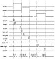
- FIG. 3 is a schematic diagram of driving sequence of a touch display panel in a display stage according to an embodiment of the present disclosure
- FIG. 4 is another schematic structural diagram of a touch display panel according to an embodiment of the present disclosure.
- FIG. 5 is another schematic structural diagram of a touch display panel according to an embodiment of the present disclosure.
- FIG. 6 is another schematic structural diagram of a touch display panel according to an embodiment of the present disclosure.
- FIG. 7 is another schematic structural diagram of a touch display panel according to an embodiment of the present disclosure.
- FIG. 7b is another schematic structural diagram of a touch display panel according to an embodiment of the present disclosure.
- a touch display panel comprising: an upper substrate 01, a lower substrate 02 and a driving chip 03 disposed opposite to the upper substrate 01, and a plurality of pixels and a common electrode layer 04 arranged in a matrix between the substrate 01 and the lower substrate 02, wherein the common electrode layer 04 is divided into a plurality of independent self-capacitance electrodes 05, and the self-capacitance electrodes 05 are connected to the corresponding wires 06 through
- the driving chip 03 has a row of self-capacitance electrodes 05 corresponding to a plurality of rows of pixels; the driving chip 03 is configured to perform progressive scanning on the pixels, and only when the pixels corresponding to the respective rows of self-capacitance electrodes 05 are in a scanning state, the corresponding row self-capacitance Electrode 05 applies a common electrode signal.
- the position of the driving chip 03 may also be disposed at other positions than the lower substrate 02. In other words, the position of the driving chip 03 is not limited to being disposed opposite to the upper substrate 01. Moreover, in other embodiments, each row of self-capacitance electrodes 05 may also correspond to a single row of pixels.
- the driving timing of the touch display panel can be as shown in FIG. 3, when scanning the pixels of the first to n rows, the driving chip 3 is A row of self-capacitance electrodes applies a common voltage signal Vcom1. Similarly, when scanning the n+1th to 2nth rows of pixels, the driver chip 3 can apply a common voltage signal Vcom2 to the row of self-capacitance electrodes corresponding thereto.
- the driving chip 3 can apply a common voltage signal Vcomx to the row of self-capacitance electrodes corresponding thereto, that is, only when the pixels corresponding to the respective rows of self-capacitance electrodes are in a scanning state, correspondingly A common electrode signal is applied from the capacitor electrode.
- the scanning of the n-th row of pixels refers to applying a scan signal to the gate line gate corresponding to the row of pixels, and applying a data signal to the data line Data corresponding to the row of pixels.
- the touch display panel may include an upper substrate, a lower substrate disposed opposite the upper substrate, a driving chip, a plurality of pixels arranged in a matrix between the upper substrate and the lower substrate, and a common electrode layer.
- the common electrode layer is divided into a plurality of independent self-capacitance electrodes, and the self-capacitance electrodes are connected to the driving chip through corresponding wires, and each row of self-capacitance electrodes can correspond to a plurality of rows of pixels; the driving chip is configured to perform progressive scanning on the pixels And applying a common electrode signal to the corresponding row of self-capacitance electrodes only when the pixels corresponding to the respective rows of self-capacitance electrodes are in a scanning state.
- the common electrode signals are applied to the corresponding row self-capacitance electrodes, thereby reducing the amount of data required to be processed by the driving circuit, thereby The design of the drive circuit is simplified, and the production cost is saved.
- the touch display panel provided by some embodiments of the present disclosure does not need to add an additional film layer, and only needs to pattern the common electrode layer disposed in the original layer to form a corresponding self-capacitance electrode pattern, thereby saving Production costs increase production efficiency.
- the touch electrode density of the touch screen is usually on the order of millimeters. Therefore, in a specific implementation, the density and the occupied area of each "self-capacitance electrode" can be selected according to the required touch density to ensure the required touch density.
- each "self-capacitance electrode” is designed as a square electrode of about 5 mm * 5 mm.
- the pixel density of the display screen is usually on the order of micrometers. Therefore, generally one self-capacitance electrode corresponds to a plurality of pixel units in the display screen.
- the touch display panel provided by some embodiments of the present disclosure divides the common electrode layer disposed on the upper substrate into a plurality of self-capacitance electrodes and corresponding wires.
- a self-capacitance electrode of a regular arrangement is obtained.
- the number of rows of pixels corresponding to each row of self-capacitance electrodes is the same.
- the method further includes: a plurality of compensation resistors Rn electrically connected to the plurality of wires 06, and each of the compensation resistors Rn
- the resistance value is inversely related to the length of the corresponding wire 06. That is, the longer the wire, the smaller the resistance value of the compensation resistor Rn to which the wire is connected.
- the difference in the load of the output due to the difference in the length of the wires connected between the driving chip and the self-capacitance electrode is improved by connecting a compensation resistor to the wire, so that the uniformity of display is improved.
- the setting of the resistance value of the compensation resistor is to detect the output difference of each wire load by applying a common electrode signal to each wire in advance, determine the resistance value of the resistance according to the difference, and then set the compensation of the corresponding resistance value.
- the resistance is such that the resistance of each wire is equal to the sum of the resistances connected to the wires, thereby improving the uniformity of display.
- the touch display panel provided by the other embodiments of the present disclosure, as shown in FIG. 5, further includes: a plurality of compensation capacitors Cn coupled to the plurality of wires 06, and a capacitance value of each compensation capacitor Cn. It is inversely related to the length of the corresponding wire 06, wherein the compensation capacitor Cn comprises a first electrode and a second electrode. The difference in the load of the output due to the difference in the length of the wires connected between the driving chip and the self-capacitance electrode is improved by connecting the compensation capacitor to the wire, so that the uniformity of display is improved.
- the setting of the capacitance value of the compensation capacitor is obtained by testing in advance, and then the compensation capacitor of the corresponding capacitance value is set according to the obtained value, so that the wires have the same load, thereby improving display uniformity.
- the first electrode 07 of the compensation capacitor is disposed in the same layer as the wire 06, and the first electrode 07 and the wire 06 are disposed above
- the insulating layer 09, the self-capacitance electrode 05 and the second electrode 08 are disposed in the same layer, and the self-capacitance electrode 05 is connected to the wire 06 through the via hole, so that in the preparation, the preparation process of the first electrode is not separately added, and only the original wire is required to be changed.
- the patterning of the film layer can be realized, which simplifies the process steps, saves production costs and improves production efficiency.
- the touch display panel provided by some embodiments of the present disclosure, a part of the wire 06 is multiplexed into the first electrode, that is, utilized.
- the wire and the second electrode 08 constitute a compensation capacitor.
- the second electrode 08 disposed above it has a smaller area, and for a shorter length of wire 062, a portion disposed above it
- the two electrodes 08 have a large area, thereby forming compensation capacitors of different sizes.
- the second electrodes 08 above the wires 06 having different lengths are different in area, thereby forming compensation capacitors of different sizes. .
- the second electrode 08 and the self-capacitance electrode 05 are further simplified in order to further simplify the process steps. Same layer setting. Therefore, in the preparation, the preparation process of the second electrode is not separately added, and only the composition of the film layer corresponding to the original self-capacitance electrode can be changed, the process step is simplified, the production cost is saved, and the production efficiency is improved.
- the touch display panel provided by some embodiments of the present disclosure, when the wires are disposed in the same layer as the self-capacitance electrodes, since the first electrodes are disposed in the same layer as the wires or are multiplexed by the wires, in order to ensure that the first electrodes are
- the second electrode has a large facing area, and the second electrode is disposed in a different layer from the self-capacitance electrode.
- a data line is further included, and the wire extending direction is the same as the data line extending direction.
- the wires are disposed in the same layer and insulated from the data lines. Therefore, in the preparation, it is not necessary to separately increase the preparation process of the wire, and only the composition of the film layer corresponding to the original data line needs to be changed, the process step is simplified, the production cost is saved, and the production efficiency is improved.
- the driving chip is further configured to apply a touch scan signal to each “self-capacitance electrode” during touch control, by detecting each “self-capacitance electrode”.
- the capacitance value changes to determine the touch position.
- the specific principle is: when the human body does not touch the screen, the capacitance of each "self-capacitance electrode” is a fixed value. When the human body touches the screen, the capacitance of the corresponding self-capacitance electrode is a fixed value superimposed on the human body capacitance.
- the driving chip can determine the touch position by detecting the change of the capacitance value of each "self-capacitance electrode” in the touch timing section.
- the driving chip can simultaneously apply a touch scan signal to the self-capacitance electrode, or apply a touch scan signal to the self-capacitance electrode line by line, which is not limited herein.
- the touch scan signal can be a square wave signal.
- the touch display panel provided by some embodiments of the present disclosure divides the common electrode layer disposed in the entire entire layer into a plurality of self-capacitance electrodes, in order not to affect the normal display function, in the common electrode layer.
- the dividing line generally avoids the open area of the display and is placed in the graphic area of the black matrix layer.
- the above-mentioned touch screen may further include: a black matrix layer disposed on a side of the upper substrate facing the lower substrate or a side of the lower substrate facing the upper substrate;
- the orthogonal projection between the adjacent two self-capacitance electrodes is located in the area where the pattern of the black matrix layer is located in the area where the pattern of the black matrix layer is located;
- the pattern of each of the wires is located in the area where the pattern of the black matrix layer is located in the orthographic projection of the lower substrate.
- some embodiments of the present disclosure further provide a display device, including a touch display panel provided by some embodiments of the present disclosure, which may be: a mobile phone, a tablet computer, a television, a display, a notebook computer, a digital device. Any product or component that has a display function, such as a photo frame or a navigator.
- a display device including a touch display panel provided by some embodiments of the present disclosure, which may be: a mobile phone, a tablet computer, a television, a display, a notebook computer, a digital device. Any product or component that has a display function, such as a photo frame or a navigator.
- the display device reference may be made to the above embodiment of the in-cell touch panel, and the repeated description is omitted.
- some embodiments of the present disclosure further provide a driving method of a touch display panel, where the driving method includes:
- the pixels in the touch display panel are progressively scanned, and the common electrode signal is applied to the self-capacitance electrodes of the row only when the pixels corresponding to the respective rows of self-capacitance electrodes are scanned.
- the driving method of the touch display panel controls the timing of applying the common electrode signals to the self-capacitance electrodes of each row, that is, only when scanning the pixels corresponding to the “self-capacitance electrodes”
- the capacitor electrode applies a common electrode signal to reduce the amount of data required to be processed by the driving circuit, thereby simplifying the design of the driving circuit and saving production costs.
- the driving method provided by some embodiments of the present disclosure may further include:
- the touch position is determined by detecting a change in the capacitance value of each "self-capacitance electrode”.
- each "self-capacitance electrode” When the human body does not touch the screen, the capacitance of each "self-capacitance electrode" is a fixed value. When the human body touches the screen, the capacitance of the corresponding self-capacitance electrode is a fixed value superimposed on the human body capacitance, and the driving chip is in contact.
- the control timing segment can determine the touch position by detecting the change in the capacitance value of each "self-capacitance electrode".
- each row of self-capacitance electrodes corresponds to n rows of pixels, where n is an integer greater than or equal to 1, and the driving method is specifically:
- the pixels in the touch display panel are progressively scanned, and only when n rows of pixels corresponding to the respective rows of self-capacitance electrodes are scanned, a common electrode signal is applied to the corresponding row of self-capacitance electrodes.
Landscapes
- Engineering & Computer Science (AREA)
- General Engineering & Computer Science (AREA)
- Theoretical Computer Science (AREA)
- Human Computer Interaction (AREA)
- Physics & Mathematics (AREA)
- General Physics & Mathematics (AREA)
- Computer Networks & Wireless Communication (AREA)
- Position Input By Displaying (AREA)
- Control Of Indicators Other Than Cathode Ray Tubes (AREA)
- Liquid Crystal (AREA)
Abstract
Description
Claims (18)
- 一种触控显示面板的驱动方法,其中,所述触控显示面板包括:上基板;与所述上基板相对设置的下基板;位于所述上基板与所述下基板之间呈矩阵排列的多个像素;位于所述上基板与所述下基板之间的公共电极层,其被分割成多个相互独立的自电容电极;以及驱动芯片,通过对应导线连接至所述自电容电极;所述驱动方法包括:在显示时,所述驱动芯片对所述触控显示面板中像素进行逐行扫描,且仅当扫描与各行自电容电极对应的像素时,对相应行自电容电极施加公共电极信号。
- 如权利要求1所述的驱动方法,还包括:在触控时,通过检测各所述自电容电极的电容值变化以判断触控位置。
- 如权利要求1所述的驱动方法,其中,所述触控显示面板还包括:与多根导线分别电连接的多个补偿电阻,每个补偿电阻的电阻值与相应导线的长度负相关。
- 如权利要求1所述的驱动方法,其中,所述触控显示面板还包括:与多根导线分别耦接的多个补偿电容,每个补偿电容的电容值与相应导线的长度负相关。
- 如权利要求1所述的驱动方法,其中,每行自电容电极对应n行像素,其中n为大于等于1的整数,所述驱动方法具体为:在显示时,对触控显示面板中像素进行逐行扫描,且仅当对各行自电容电极对应的n行像素进行扫描时,对相应行自电容电极施加公共电极信号。
- 一种触控显示面板,包括:上基板;与所述上基板相对设置的下基板;位于所述上基板与所述下基板之间呈矩阵排列的多个像素;驱动芯片,被配置为对所述多个像素进行逐行扫描;以及位于所述上基板与所述下基板之间的公共电极层,其被分割成多个相互独立的自电容电极,所述自电容电极通过对应导线连接至所述驱动芯片,其中,所述驱动芯片还被配置为仅在与各行自电容电极对应的像素处于扫描状态,对相应行自电容电极施加公共电极信号。
- 如权利要求6所述的触控显示面板,其中,每一行自电容电极对应多行像素。
- 如权利要求7所述的触控显示面板,其中,每行自电容电极对应的像素行数相同。
- 如权利要求6所述的触控显示面板,还包括:与多根导线分别电连接的多个补偿电阻,每个补偿电阻的电阻值与相应导线的长度负相关。
- 如权利要求6所述的触控显示面板,还包括:与多根导线分别耦接的多个补偿电容,每个补偿电容的电容值与相应导线的长度负相关。
- 如权利要求10所述的触控显示面板,其中,补偿电容的第一电极与所述导线同层设置。
- 如权利要求10所述的触控显示面板,其中,所述导线的一部分复用为所述补偿电容的第一电极。
- 如权利要求11或12所述的触控显示面板,其中,所述导线与所述自电容电极异层设置,所述补偿电容的第二电极与所述自电容电极同层设置。
- 如权利要求11或12所述的触控显示面板,其中,所述导线与所述自电容电极同层设置,所述补偿电容的第二电极与所述自电容电极异层设置。
- 如权利要求6-14任一项所述的触控显示面板,还包括:数据线,其延伸方向与所述导线延伸方向相同。
- 如权利要求15所述的触控显示面板,其中,所述导线与所述数据线同层且绝缘设置。
- 如权利要求6-16任一项所述的触控显示面板,其中,所述驱动芯片还被配置为:在触控时,通过检测各所述自电容电极的电容值变化以判断触控 位置。
- 一种显示装置,包括如权利要求6-17任一项所述的触控显示面板。
Priority Applications (1)
| Application Number | Priority Date | Filing Date | Title |
|---|---|---|---|
| US16/068,927 US10949007B2 (en) | 2017-05-18 | 2017-12-15 | Touch display panel, display apparatus, and method for driving touch display panel |
Applications Claiming Priority (2)
| Application Number | Priority Date | Filing Date | Title |
|---|---|---|---|
| CN201710353151.9 | 2017-05-18 | ||
| CN201710353151.9A CN108958523A (zh) | 2017-05-18 | 2017-05-18 | 一种触控显示面板、显示装置及触控显示面板的驱动方法 |
Publications (1)
| Publication Number | Publication Date |
|---|---|
| WO2018209946A1 true WO2018209946A1 (zh) | 2018-11-22 |
Family
ID=64273306
Family Applications (1)
| Application Number | Title | Priority Date | Filing Date |
|---|---|---|---|
| PCT/CN2017/116517 Ceased WO2018209946A1 (zh) | 2017-05-18 | 2017-12-15 | 触控显示面板、显示装置及触控显示面板的驱动方法 |
Country Status (3)
| Country | Link |
|---|---|
| US (1) | US10949007B2 (zh) |
| CN (1) | CN108958523A (zh) |
| WO (1) | WO2018209946A1 (zh) |
Cited By (2)
| Publication number | Priority date | Publication date | Assignee | Title |
|---|---|---|---|---|
| TWI696106B (zh) * | 2019-06-24 | 2020-06-11 | 大陸商北京集創北方科技股份有限公司 | 圓形觸控屏感測方法、觸控顯示裝置及資訊處理裝置 |
| EP3779653A1 (en) * | 2019-08-12 | 2021-02-17 | LG Display Co., Ltd. | Touch display device |
Families Citing this family (6)
| Publication number | Priority date | Publication date | Assignee | Title |
|---|---|---|---|---|
| US11101856B2 (en) * | 2019-08-16 | 2021-08-24 | Lg Electronics Inc. | Method and apparatus for uplink signal transmission based on codebook in a wireless communication system |
| US11095348B2 (en) | 2019-08-16 | 2021-08-17 | Lg Electronics Inc. | Method and apparatus for uplink signal transmission based on codebook in a wireless communication system |
| US11231807B1 (en) | 2020-08-14 | 2022-01-25 | Apple Inc. | Touch sensor panel including resistors for improved input signal |
| CN114253430B (zh) * | 2021-12-06 | 2024-01-19 | 厦门天马微电子有限公司 | 显示面板和显示装置 |
| CN115236906B (zh) * | 2022-06-30 | 2023-08-22 | 苏州华星光电技术有限公司 | 显示装置 |
| CN119902643B (zh) * | 2024-07-29 | 2025-10-28 | 合肥维信诺科技有限公司 | 触控面板、显示设备和触控扫描方法 |
Citations (3)
| Publication number | Priority date | Publication date | Assignee | Title |
|---|---|---|---|---|
| CN104020891A (zh) * | 2014-05-30 | 2014-09-03 | 京东方科技集团股份有限公司 | 一种内嵌式触摸屏及显示装置 |
| CN104680999A (zh) * | 2015-03-19 | 2015-06-03 | 京东方科技集团股份有限公司 | 一种具有触控功能的显示基板及其驱动方法、显示装置 |
| CN104777942A (zh) * | 2015-05-08 | 2015-07-15 | 厦门天马微电子有限公司 | 触控显示面板、驱动方法及触控显示装置 |
Family Cites Families (7)
| Publication number | Priority date | Publication date | Assignee | Title |
|---|---|---|---|---|
| CN101963715B (zh) * | 2009-07-24 | 2013-05-22 | 群康科技(深圳)有限公司 | 触控显示器 |
| CN102455532B (zh) * | 2010-10-26 | 2015-12-02 | 上海天马微电子有限公司 | 液晶显示装置触摸检测单元、触摸显示单元和检测方法 |
| KR20140086477A (ko) * | 2012-12-28 | 2014-07-08 | 삼성전기주식회사 | 터치 감지 장치 |
| KR102052750B1 (ko) * | 2013-05-31 | 2019-12-06 | 엘지디스플레이 주식회사 | 터치 스크린 구동 장치 |
| CN104536630B (zh) * | 2015-01-21 | 2017-05-10 | 京东方科技集团股份有限公司 | 一种触摸显示面板、其检测方法及显示装置 |
| US9921696B2 (en) * | 2015-04-24 | 2018-03-20 | Apple Inc. | Sensor with diffusing resistor |
| TWI557715B (zh) * | 2015-05-14 | 2016-11-11 | 友達光電股份有限公司 | 顯示面板 |
-
2017
- 2017-05-18 CN CN201710353151.9A patent/CN108958523A/zh active Pending
- 2017-12-15 WO PCT/CN2017/116517 patent/WO2018209946A1/zh not_active Ceased
- 2017-12-15 US US16/068,927 patent/US10949007B2/en not_active Expired - Fee Related
Patent Citations (3)
| Publication number | Priority date | Publication date | Assignee | Title |
|---|---|---|---|---|
| CN104020891A (zh) * | 2014-05-30 | 2014-09-03 | 京东方科技集团股份有限公司 | 一种内嵌式触摸屏及显示装置 |
| CN104680999A (zh) * | 2015-03-19 | 2015-06-03 | 京东方科技集团股份有限公司 | 一种具有触控功能的显示基板及其驱动方法、显示装置 |
| CN104777942A (zh) * | 2015-05-08 | 2015-07-15 | 厦门天马微电子有限公司 | 触控显示面板、驱动方法及触控显示装置 |
Cited By (3)
| Publication number | Priority date | Publication date | Assignee | Title |
|---|---|---|---|---|
| TWI696106B (zh) * | 2019-06-24 | 2020-06-11 | 大陸商北京集創北方科技股份有限公司 | 圓形觸控屏感測方法、觸控顯示裝置及資訊處理裝置 |
| EP3779653A1 (en) * | 2019-08-12 | 2021-02-17 | LG Display Co., Ltd. | Touch display device |
| US11231799B2 (en) | 2019-08-12 | 2022-01-25 | Lg Display Co., Ltd. | Touch display device |
Also Published As
| Publication number | Publication date |
|---|---|
| US20200174604A1 (en) | 2020-06-04 |
| US10949007B2 (en) | 2021-03-16 |
| CN108958523A (zh) | 2018-12-07 |
Similar Documents
| Publication | Publication Date | Title |
|---|---|---|
| WO2018209946A1 (zh) | 触控显示面板、显示装置及触控显示面板的驱动方法 | |
| US10268304B2 (en) | Touch display panel, manufacturing method for the same, driving method for the same, and display device | |
| CN104022128B (zh) | 一种阵列基板及其制作方法、以及显示装置 | |
| CN104022127B (zh) | 一种阵列基板及其制作方法、以及显示装置 | |
| CN104020912B (zh) | 电容式触摸结构、内嵌式触摸屏、显示装置及其扫描方法 | |
| CN105094422B (zh) | 一种触控显示面板、其制备方法、驱动方法及显示装置 | |
| CN103294312B (zh) | 电容式触摸屏、电容式触摸屏制备方法及显示装置 | |
| CN106908980B (zh) | 阵列基板、触控显示面板及显示装置 | |
| CN104571765B (zh) | 一种内嵌式触摸屏及显示装置 | |
| CN104991690B (zh) | 一种触控显示面板、其制作方法、驱动方法及显示装置 | |
| WO2016115781A1 (zh) | 一种触摸显示面板、其检测方法及显示装置 | |
| WO2015180322A1 (zh) | 内嵌式触摸屏以及显示装置 | |
| WO2015117288A1 (zh) | 内嵌式触摸屏及显示装置 | |
| WO2015180316A1 (zh) | 内嵌式触摸屏及显示装置 | |
| WO2015180313A1 (zh) | 内嵌式触摸屏及显示装置 | |
| WO2015180303A1 (zh) | 内嵌式触摸屏及显示装置 | |
| WO2016119333A1 (zh) | 内嵌式触摸屏及其驱动方法以及显示装置 | |
| WO2015180312A1 (zh) | 内嵌式触摸屏及显示装置 | |
| EP3118727B1 (en) | In-cell touchscreen and display device | |
| WO2016112683A1 (zh) | 内嵌式触摸屏及显示装置 | |
| US20200319739A1 (en) | Touch display panel | |
| WO2015180347A1 (zh) | 一种阵列基板及其制备方法、内嵌式触摸屏及显示装置 | |
| WO2016110045A1 (zh) | 内嵌式触摸屏及显示装置 | |
| WO2015135289A1 (zh) | 内嵌式触摸屏及显示装置 | |
| WO2015010376A1 (zh) | 阵列基板及其制造方法、触摸屏和显示装置 |
Legal Events
| Date | Code | Title | Description |
|---|---|---|---|
| 121 | Ep: the epo has been informed by wipo that ep was designated in this application |
Ref document number: 17910221 Country of ref document: EP Kind code of ref document: A1 |
|
| NENP | Non-entry into the national phase |
Ref country code: DE |
|
| 122 | Ep: pct application non-entry in european phase |
Ref document number: 17910221 Country of ref document: EP Kind code of ref document: A1 |
|
| 32PN | Ep: public notification in the ep bulletin as address of the adressee cannot be established |
Free format text: NOTING OF LOSS OF RIGHTS PURSUANT TO RULE 112(1) EPC (EPO FORM 1205N DATED 21/01/2020) |
|
| 122 | Ep: pct application non-entry in european phase |
Ref document number: 17910221 Country of ref document: EP Kind code of ref document: A1 |